US9705204B2 - Low-profile wireless connectors - Google Patents
Low-profile wireless connectors Download PDFInfo
- Publication number
- US9705204B2 US9705204B2 US13/657,476 US201213657476A US9705204B2 US 9705204 B2 US9705204 B2 US 9705204B2 US 201213657476 A US201213657476 A US 201213657476A US 9705204 B2 US9705204 B2 US 9705204B2
- Authority
- US
- United States
- Prior art keywords
- pcb
- communication unit
- antenna
- electronic device
- ehf
- Prior art date
- Legal status (The legal status is an assumption and is not a legal conclusion. Google has not performed a legal analysis and makes no representation as to the accuracy of the status listed.)
- Active, expires
Links
- 238000004891 communication Methods 0.000 claims abstract description 222
- 239000004020 conductor Substances 0.000 claims abstract description 37
- 230000005670 electromagnetic radiation Effects 0.000 claims abstract description 26
- 239000000463 material Substances 0.000 claims description 17
- 230000010287 polarization Effects 0.000 claims description 14
- 239000000758 substrate Substances 0.000 description 18
- 238000000034 method Methods 0.000 description 17
- 230000005855 radiation Effects 0.000 description 6
- MTCPZNVSDFCBBE-UHFFFAOYSA-N 1,3,5-trichloro-2-(2,6-dichlorophenyl)benzene Chemical compound ClC1=CC(Cl)=CC(Cl)=C1C1=C(Cl)C=CC=C1Cl MTCPZNVSDFCBBE-UHFFFAOYSA-N 0.000 description 5
- 230000008901 benefit Effects 0.000 description 4
- 238000004519 manufacturing process Methods 0.000 description 4
- 238000012546 transfer Methods 0.000 description 4
- 230000015556 catabolic process Effects 0.000 description 2
- 238000006731 degradation reaction Methods 0.000 description 2
- 238000013461 design Methods 0.000 description 2
- 239000011810 insulating material Substances 0.000 description 2
- 239000004065 semiconductor Substances 0.000 description 2
- 230000008054 signal transmission Effects 0.000 description 2
- 229910000679 solder Inorganic materials 0.000 description 2
- 238000001228 spectrum Methods 0.000 description 2
- 230000005540 biological transmission Effects 0.000 description 1
- 239000000919 ceramic Substances 0.000 description 1
- 150000001875 compounds Chemical class 0.000 description 1
- 230000008878 coupling Effects 0.000 description 1
- 238000010168 coupling process Methods 0.000 description 1
- 238000005859 coupling reaction Methods 0.000 description 1
- 238000011161 development Methods 0.000 description 1
- 230000000694 effects Effects 0.000 description 1
- 238000010292 electrical insulation Methods 0.000 description 1
- 238000005516 engineering process Methods 0.000 description 1
- 230000002708 enhancing effect Effects 0.000 description 1
- 239000011521 glass Substances 0.000 description 1
- 238000001465 metallisation Methods 0.000 description 1
- 238000012986 modification Methods 0.000 description 1
- 230000004048 modification Effects 0.000 description 1
- 239000004033 plastic Substances 0.000 description 1
- 238000012545 processing Methods 0.000 description 1
- 229910052710 silicon Inorganic materials 0.000 description 1
- 239000010703 silicon Substances 0.000 description 1
Images


Classifications
-
- H—ELECTRICITY
- H01—ELECTRIC ELEMENTS
- H01Q—ANTENNAS, i.e. RADIO AERIALS
- H01Q21/00—Antenna arrays or systems
- H01Q21/24—Combinations of antenna units polarised in different directions for transmitting or receiving circularly and elliptically polarised waves or waves linearly polarised in any direction
-
- H04B5/72—
-
- H—ELECTRICITY
- H01—ELECTRIC ELEMENTS
- H01L—SEMICONDUCTOR DEVICES NOT COVERED BY CLASS H10
- H01L23/00—Details of semiconductor or other solid state devices
- H01L23/48—Arrangements for conducting electric current to or from the solid state body in operation, e.g. leads, terminal arrangements ; Selection of materials therefor
- H01L23/488—Arrangements for conducting electric current to or from the solid state body in operation, e.g. leads, terminal arrangements ; Selection of materials therefor consisting of soldered or bonded constructions
- H01L23/495—Lead-frames or other flat leads
- H01L23/49503—Lead-frames or other flat leads characterised by the die pad
- H01L23/4951—Chip-on-leads or leads-on-chip techniques, i.e. inner lead fingers being used as die pad
-
- H—ELECTRICITY
- H01—ELECTRIC ELEMENTS
- H01L—SEMICONDUCTOR DEVICES NOT COVERED BY CLASS H10
- H01L23/00—Details of semiconductor or other solid state devices
- H01L23/58—Structural electrical arrangements for semiconductor devices not otherwise provided for, e.g. in combination with batteries
- H01L23/64—Impedance arrangements
- H01L23/66—High-frequency adaptations
-
- H—ELECTRICITY
- H01—ELECTRIC ELEMENTS
- H01Q—ANTENNAS, i.e. RADIO AERIALS
- H01Q1/00—Details of, or arrangements associated with, antennas
- H01Q1/36—Structural form of radiating elements, e.g. cone, spiral, umbrella; Particular materials used therewith
-
- H—ELECTRICITY
- H04—ELECTRIC COMMUNICATION TECHNIQUE
- H04B—TRANSMISSION
- H04B5/00—Near-field transmission systems, e.g. inductive loop type
- H04B5/0025—Near field system adaptations
- H04B5/0031—Near field system adaptations for data transfer
-
- H—ELECTRICITY
- H05—ELECTRIC TECHNIQUES NOT OTHERWISE PROVIDED FOR
- H05K—PRINTED CIRCUITS; CASINGS OR CONSTRUCTIONAL DETAILS OF ELECTRIC APPARATUS; MANUFACTURE OF ASSEMBLAGES OF ELECTRICAL COMPONENTS
- H05K1/00—Printed circuits
- H05K1/02—Details
- H05K1/0213—Electrical arrangements not otherwise provided for
- H05K1/0237—High frequency adaptations
- H05K1/0239—Signal transmission by AC coupling
-
- H—ELECTRICITY
- H01—ELECTRIC ELEMENTS
- H01L—SEMICONDUCTOR DEVICES NOT COVERED BY CLASS H10
- H01L2223/00—Details relating to semiconductor or other solid state devices covered by the group H01L23/00
- H01L2223/58—Structural electrical arrangements for semiconductor devices not otherwise provided for
- H01L2223/64—Impedance arrangements
- H01L2223/66—High-frequency adaptations
- H01L2223/6661—High-frequency adaptations for passive devices
- H01L2223/6677—High-frequency adaptations for passive devices for antenna, e.g. antenna included within housing of semiconductor device
-
- H—ELECTRICITY
- H01—ELECTRIC ELEMENTS
- H01L—SEMICONDUCTOR DEVICES NOT COVERED BY CLASS H10
- H01L2224/00—Indexing scheme for arrangements for connecting or disconnecting semiconductor or solid-state bodies and methods related thereto as covered by H01L24/00
- H01L2224/01—Means for bonding being attached to, or being formed on, the surface to be connected, e.g. chip-to-package, die-attach, "first-level" interconnects; Manufacturing methods related thereto
- H01L2224/42—Wire connectors; Manufacturing methods related thereto
- H01L2224/47—Structure, shape, material or disposition of the wire connectors after the connecting process
- H01L2224/48—Structure, shape, material or disposition of the wire connectors after the connecting process of an individual wire connector
- H01L2224/4805—Shape
- H01L2224/4809—Loop shape
- H01L2224/48091—Arched
-
- H—ELECTRICITY
- H01—ELECTRIC ELEMENTS
- H01L—SEMICONDUCTOR DEVICES NOT COVERED BY CLASS H10
- H01L2224/00—Indexing scheme for arrangements for connecting or disconnecting semiconductor or solid-state bodies and methods related thereto as covered by H01L24/00
- H01L2224/73—Means for bonding being of different types provided for in two or more of groups H01L2224/10, H01L2224/18, H01L2224/26, H01L2224/34, H01L2224/42, H01L2224/50, H01L2224/63, H01L2224/71
- H01L2224/732—Location after the connecting process
- H01L2224/73251—Location after the connecting process on different surfaces
- H01L2224/73265—Layer and wire connectors
-
- H—ELECTRICITY
- H01—ELECTRIC ELEMENTS
- H01L—SEMICONDUCTOR DEVICES NOT COVERED BY CLASS H10
- H01L2924/00—Indexing scheme for arrangements or methods for connecting or disconnecting semiconductor or solid-state bodies as covered by H01L24/00
-
- H—ELECTRICITY
- H01—ELECTRIC ELEMENTS
- H01L—SEMICONDUCTOR DEVICES NOT COVERED BY CLASS H10
- H01L2924/00—Indexing scheme for arrangements or methods for connecting or disconnecting semiconductor or solid-state bodies as covered by H01L24/00
- H01L2924/0001—Technical content checked by a classifier
- H01L2924/00014—Technical content checked by a classifier the subject-matter covered by the group, the symbol of which is combined with the symbol of this group, being disclosed without further technical details
-
- H—ELECTRICITY
- H01—ELECTRIC ELEMENTS
- H01L—SEMICONDUCTOR DEVICES NOT COVERED BY CLASS H10
- H01L2924/00—Indexing scheme for arrangements or methods for connecting or disconnecting semiconductor or solid-state bodies as covered by H01L24/00
- H01L2924/10—Details of semiconductor or other solid state devices to be connected
- H01L2924/11—Device type
- H01L2924/14—Integrated circuits
-
- H—ELECTRICITY
- H01—ELECTRIC ELEMENTS
- H01L—SEMICONDUCTOR DEVICES NOT COVERED BY CLASS H10
- H01L2924/00—Indexing scheme for arrangements or methods for connecting or disconnecting semiconductor or solid-state bodies as covered by H01L24/00
- H01L2924/15—Details of package parts other than the semiconductor or other solid state devices to be connected
- H01L2924/151—Die mounting substrate
- H01L2924/153—Connection portion
- H01L2924/1531—Connection portion the connection portion being formed only on the surface of the substrate opposite to the die mounting surface
- H01L2924/15311—Connection portion the connection portion being formed only on the surface of the substrate opposite to the die mounting surface being a ball array, e.g. BGA
-
- H—ELECTRICITY
- H01—ELECTRIC ELEMENTS
- H01L—SEMICONDUCTOR DEVICES NOT COVERED BY CLASS H10
- H01L2924/00—Indexing scheme for arrangements or methods for connecting or disconnecting semiconductor or solid-state bodies as covered by H01L24/00
- H01L2924/30—Technical effects
- H01L2924/301—Electrical effects
- H01L2924/3011—Impedance
-
- H—ELECTRICITY
- H05—ELECTRIC TECHNIQUES NOT OTHERWISE PROVIDED FOR
- H05K—PRINTED CIRCUITS; CASINGS OR CONSTRUCTIONAL DETAILS OF ELECTRIC APPARATUS; MANUFACTURE OF ASSEMBLAGES OF ELECTRICAL COMPONENTS
- H05K1/00—Printed circuits
- H05K1/02—Details
- H05K1/0213—Electrical arrangements not otherwise provided for
- H05K1/0237—High frequency adaptations
- H05K1/0243—Printed circuits associated with mounted high frequency components
-
- H—ELECTRICITY
- H05—ELECTRIC TECHNIQUES NOT OTHERWISE PROVIDED FOR
- H05K—PRINTED CIRCUITS; CASINGS OR CONSTRUCTIONAL DETAILS OF ELECTRIC APPARATUS; MANUFACTURE OF ASSEMBLAGES OF ELECTRICAL COMPONENTS
- H05K1/00—Printed circuits
- H05K1/02—Details
- H05K1/14—Structural association of two or more printed circuits
- H05K1/142—Arrangements of planar printed circuit boards in the same plane, e.g. auxiliary printed circuit insert mounted in a main printed circuit
-
- H—ELECTRICITY
- H05—ELECTRIC TECHNIQUES NOT OTHERWISE PROVIDED FOR
- H05K—PRINTED CIRCUITS; CASINGS OR CONSTRUCTIONAL DETAILS OF ELECTRIC APPARATUS; MANUFACTURE OF ASSEMBLAGES OF ELECTRICAL COMPONENTS
- H05K2201/00—Indexing scheme relating to printed circuits covered by H05K1/00
- H05K2201/10—Details of components or other objects attached to or integrated in a printed circuit board
- H05K2201/10007—Types of components
- H05K2201/10098—Components for radio transmission, e.g. radio frequency identification [RFID] tag, printed or non-printed antennas
-
- H—ELECTRICITY
- H05—ELECTRIC TECHNIQUES NOT OTHERWISE PROVIDED FOR
- H05K—PRINTED CIRCUITS; CASINGS OR CONSTRUCTIONAL DETAILS OF ELECTRIC APPARATUS; MANUFACTURE OF ASSEMBLAGES OF ELECTRICAL COMPONENTS
- H05K2201/00—Indexing scheme relating to printed circuits covered by H05K1/00
- H05K2201/10—Details of components or other objects attached to or integrated in a printed circuit board
- H05K2201/10431—Details of mounted components
- H05K2201/10439—Position of a single component
- H05K2201/10446—Mounted on an edge
Definitions
- the method may include disposing the first electronic device and the second electronic device such that the first EHF communication unit and the second EHF communication unit are substantially proximal and oriented substantially along a common plane so that the first EHF communication unit and the second EHF communication unit enable communication between the first electronic device and the second electronic device by mutually transmitting and receiving electromagnetic radiation in a direction along the common plane.
- Die 106 may include any suitable structure configured as a miniaturized circuit on a suitable die substrate, and is functionally equivalent to a component also referred to as a chip or an integrated circuit (IC).
- a die substrate may be any suitable semiconductor material; for example, a die substrate may be silicon.
- the die 106 may have a length and a width dimension, each of which may be about 1.0 mm to about 2.0 mm, and preferably about 1.2 mm to about 1.5 mm.
- Die 106 may be mounted with further electrical conductors, such as a lead frame, (not shown in FIG. 1 ), providing connection to external circuits. Further, a transformer (not shown) may also be provided to provide impedance matching between a circuit on die 106 and antenna 110 .
- Leads 218 may be embedded or fixed in a lead frame substrate 220 , shown in phantom lines, corresponding to package substrate 114 .
- the lead frame substrate may be any suitable insulating material configured to substantially hold leads 218 in a predetermined arrangement. Electrical communication between die 208 and leads 218 of lead frame 210 may be accomplished by any suitable method using conductive connectors 212 .
- conductive connectors 212 may include bond wires that electrically connect terminals on a circuit of die 208 with the corresponding lead conductors 218 .
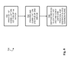
- An illustrative method of communication between a first electronic device and a second electronic device may include providing a first EHF communication unit on the first PCB of the first electronic device.
- the first EHF communication unit may have an uppermost surface having a first height from the substantially planar surface of the first PCB.
- a second EHF communication unit may be provided on the second PCB of the second electronic device, wherein the second EHF communication unit has an uppermost surface having a second height from the substantially planar surface of the second PCB.
Abstract
Description
Claims (20)
Priority Applications (1)
| Application Number | Priority Date | Filing Date | Title |
|---|---|---|---|
| US13/657,476 US9705204B2 (en) | 2011-10-20 | 2012-10-22 | Low-profile wireless connectors |
Applications Claiming Priority (2)
| Application Number | Priority Date | Filing Date | Title |
|---|---|---|---|
| US201161549378P | 2011-10-20 | 2011-10-20 | |
| US13/657,476 US9705204B2 (en) | 2011-10-20 | 2012-10-22 | Low-profile wireless connectors |
Publications (2)
| Publication Number | Publication Date |
|---|---|
| US20130106673A1 US20130106673A1 (en) | 2013-05-02 |
| US9705204B2 true US9705204B2 (en) | 2017-07-11 |
Family
ID=47178916
Family Applications (1)
| Application Number | Title | Priority Date | Filing Date |
|---|---|---|---|
| US13/657,476 Active 2032-10-26 US9705204B2 (en) | 2011-10-20 | 2012-10-22 | Low-profile wireless connectors |
Country Status (6)
| Country | Link |
|---|---|
| US (1) | US9705204B2 (en) |
| EP (1) | EP2769477A1 (en) |
| KR (1) | KR101995608B1 (en) |
| CN (1) | CN104115417A (en) |
| TW (1) | TW201325344A (en) |
| WO (1) | WO2013059801A1 (en) |
Families Citing this family (76)
| Publication number | Priority date | Publication date | Assignee | Title |
|---|---|---|---|---|
| US8554136B2 (en) | 2008-12-23 | 2013-10-08 | Waveconnex, Inc. | Tightly-coupled near-field communication-link connector-replacement chips |
| US9191263B2 (en) | 2008-12-23 | 2015-11-17 | Keyssa, Inc. | Contactless replacement for cabled standards-based interfaces |
| US9954579B2 (en) | 2008-12-23 | 2018-04-24 | Keyssa, Inc. | Smart connectors and associated communications links |
| US9219956B2 (en) * | 2008-12-23 | 2015-12-22 | Keyssa, Inc. | Contactless audio adapter, and methods |
| US9474099B2 (en) | 2008-12-23 | 2016-10-18 | Keyssa, Inc. | Smart connectors and associated communications links |
| CN103563166B (en) | 2011-03-24 | 2019-01-08 | 基萨公司 | Integrated circuit with electromagnetic communication |
| US9614590B2 (en) | 2011-05-12 | 2017-04-04 | Keyssa, Inc. | Scalable high-bandwidth connectivity |
| US8714459B2 (en) | 2011-05-12 | 2014-05-06 | Waveconnex, Inc. | Scalable high-bandwidth connectivity |
| US8811526B2 (en) | 2011-05-31 | 2014-08-19 | Keyssa, Inc. | Delta modulated low power EHF communication link |
| TWI569031B (en) | 2011-06-15 | 2017-02-01 | 奇沙公司 | Proximity sensing and distance measurement using ehf signals |
| TWI619410B (en) | 2011-09-15 | 2018-03-21 | 奇沙公司 | Wireless communication with dielectric medium |
| KR101995608B1 (en) | 2011-10-20 | 2019-10-17 | 키사, 아이엔씨. | Low-profile wireless connectors |
| TWI633766B (en) | 2011-10-21 | 2018-08-21 | 奇沙公司 | Devices and sysytems for contactless signal splicing |
| CN107257051B (en) | 2011-12-14 | 2020-01-24 | 基萨公司 | Connector providing tactile feedback |
| US9559790B2 (en) | 2012-01-30 | 2017-01-31 | Keyssa, Inc. | Link emission control |
| US9344201B2 (en) | 2012-01-30 | 2016-05-17 | Keyssa, Inc. | Shielded EHF connector assemblies |
| US9203597B2 (en) | 2012-03-02 | 2015-12-01 | Keyssa, Inc. | Systems and methods for duplex communication |
| CN104303436B (en) | 2012-03-06 | 2017-04-05 | 凯萨股份有限公司 | For the system for constraining the operating parameter of EHF communication chips |
| EP2832192B1 (en) | 2012-03-28 | 2017-09-27 | Keyssa, Inc. | Redirection of electromagnetic signals using substrate structures |
| EP2839541A1 (en) | 2012-04-17 | 2015-02-25 | Keyssa, Inc. | Dielectric lens structures for interchip communication |
| WO2014026089A1 (en) | 2012-08-10 | 2014-02-13 | Waveconnex, Inc. | Dielectric coupling systems for ehf communications |
| CN104769852B (en) | 2012-09-14 | 2016-09-21 | 凯萨股份有限公司 | There are the wireless connections of virtual magnetic hysteresis |
| CN104937769B (en) | 2012-12-17 | 2018-11-16 | 凯萨股份有限公司 | Modular electronic equipment |
| EP2974504B1 (en) | 2013-03-15 | 2018-06-20 | Keyssa, Inc. | Ehf secure communication device |
| EP2974058B1 (en) | 2013-03-15 | 2020-07-15 | Keyssa, Inc. | Contactless ehf data communication |
| KR101886739B1 (en) | 2013-03-15 | 2018-08-09 | 키사, 아이엔씨. | Extremely high frequency communication chip |
| US9325384B2 (en) * | 2013-03-15 | 2016-04-26 | Keyssa, Inc. | Misalignment-tolerant high-density multi-transmitter/receiver modules for extremely-high frequency (EHF) close-proximity wireless connections |
| US9490874B2 (en) * | 2013-10-18 | 2016-11-08 | Keyssa, Inc. | Contactless communication unit connector assemblies with signal directing structures |
| US10725150B2 (en) | 2014-12-23 | 2020-07-28 | Infineon Technologies Ag | System and method for radar |
| US10317512B2 (en) * | 2014-12-23 | 2019-06-11 | Infineon Technologies Ag | RF system with an RFIC and antenna system |
| US9602648B2 (en) | 2015-04-30 | 2017-03-21 | Keyssa Systems, Inc. | Adapter devices for enhancing the functionality of other devices |
| US10049801B2 (en) | 2015-10-16 | 2018-08-14 | Keyssa Licensing, Inc. | Communication module alignment |
| US10122420B2 (en) * | 2015-12-22 | 2018-11-06 | Intel IP Corporation | Wireless in-chip and chip to chip communication |
| US10452148B2 (en) | 2016-01-19 | 2019-10-22 | Infineon Technologies Ag | Wearable consumer device |
| US10181653B2 (en) | 2016-07-21 | 2019-01-15 | Infineon Technologies Ag | Radio frequency system for wearable device |
| US10218407B2 (en) | 2016-08-08 | 2019-02-26 | Infineon Technologies Ag | Radio frequency system and method for wearable device |
| WO2018039474A1 (en) * | 2016-08-24 | 2018-03-01 | Keyssa Systems, Inc. | Mechanical connectors for contactless communication units |
| US10466772B2 (en) | 2017-01-09 | 2019-11-05 | Infineon Technologies Ag | System and method of gesture detection for a remote device |
| US10505255B2 (en) | 2017-01-30 | 2019-12-10 | Infineon Technologies Ag | Radio frequency device packages and methods of formation thereof |
| US10602548B2 (en) | 2017-06-22 | 2020-03-24 | Infineon Technologies Ag | System and method for gesture sensing |
| US10746625B2 (en) | 2017-12-22 | 2020-08-18 | Infineon Technologies Ag | System and method of monitoring a structural object using a millimeter-wave radar sensor |
| US11278241B2 (en) | 2018-01-16 | 2022-03-22 | Infineon Technologies Ag | System and method for vital signal sensing using a millimeter-wave radar sensor |
| US11346936B2 (en) | 2018-01-16 | 2022-05-31 | Infineon Technologies Ag | System and method for vital signal sensing using a millimeter-wave radar sensor |
| US10795012B2 (en) | 2018-01-22 | 2020-10-06 | Infineon Technologies Ag | System and method for human behavior modelling and power control using a millimeter-wave radar sensor |
| US10576328B2 (en) | 2018-02-06 | 2020-03-03 | Infineon Technologies Ag | System and method for contactless sensing on a treadmill |
| US10705198B2 (en) | 2018-03-27 | 2020-07-07 | Infineon Technologies Ag | System and method of monitoring an air flow using a millimeter-wave radar sensor |
| US10775482B2 (en) | 2018-04-11 | 2020-09-15 | Infineon Technologies Ag | Human detection and identification in a setting using millimeter-wave radar |
| US10761187B2 (en) | 2018-04-11 | 2020-09-01 | Infineon Technologies Ag | Liquid detection using millimeter-wave radar sensor |
| US10794841B2 (en) | 2018-05-07 | 2020-10-06 | Infineon Technologies Ag | Composite material structure monitoring system |
| US10399393B1 (en) | 2018-05-29 | 2019-09-03 | Infineon Technologies Ag | Radar sensor system for tire monitoring |
| US10903567B2 (en) | 2018-06-04 | 2021-01-26 | Infineon Technologies Ag | Calibrating a phased array system |
| US11416077B2 (en) | 2018-07-19 | 2022-08-16 | Infineon Technologies Ag | Gesture detection system and method using a radar sensor |
| US10928501B2 (en) | 2018-08-28 | 2021-02-23 | Infineon Technologies Ag | Target detection in rainfall and snowfall conditions using mmWave radar |
| US11183772B2 (en) | 2018-09-13 | 2021-11-23 | Infineon Technologies Ag | Embedded downlight and radar system |
| US11125869B2 (en) | 2018-10-16 | 2021-09-21 | Infineon Technologies Ag | Estimating angle of human target using mmWave radar |
| US11397239B2 (en) | 2018-10-24 | 2022-07-26 | Infineon Technologies Ag | Radar sensor FSM low power mode |
| US11360185B2 (en) | 2018-10-24 | 2022-06-14 | Infineon Technologies Ag | Phase coded FMCW radar |
| EP3654053A1 (en) | 2018-11-14 | 2020-05-20 | Infineon Technologies AG | Package with acoustic sensing device(s) and millimeter wave sensing elements |
| US11087115B2 (en) | 2019-01-22 | 2021-08-10 | Infineon Technologies Ag | User authentication using mm-Wave sensor for automotive radar systems |
| US11355838B2 (en) | 2019-03-18 | 2022-06-07 | Infineon Technologies Ag | Integration of EBG structures (single layer/multi-layer) for isolation enhancement in multilayer embedded packaging technology at mmWave |
| US11126885B2 (en) | 2019-03-21 | 2021-09-21 | Infineon Technologies Ag | Character recognition in air-writing based on network of radars |
| US11454696B2 (en) | 2019-04-05 | 2022-09-27 | Infineon Technologies Ag | FMCW radar integration with communication system |
| US11327167B2 (en) | 2019-09-13 | 2022-05-10 | Infineon Technologies Ag | Human target tracking system and method |
| US11774592B2 (en) | 2019-09-18 | 2023-10-03 | Infineon Technologies Ag | Multimode communication and radar system resource allocation |
| US11435443B2 (en) | 2019-10-22 | 2022-09-06 | Infineon Technologies Ag | Integration of tracking with classifier in mmwave radar |
| US11808883B2 (en) | 2020-01-31 | 2023-11-07 | Infineon Technologies Ag | Synchronization of multiple mmWave devices |
| US11614516B2 (en) | 2020-02-19 | 2023-03-28 | Infineon Technologies Ag | Radar vital signal tracking using a Kalman filter |
| US11585891B2 (en) | 2020-04-20 | 2023-02-21 | Infineon Technologies Ag | Radar-based vital sign estimation |
| US11567185B2 (en) | 2020-05-05 | 2023-01-31 | Infineon Technologies Ag | Radar-based target tracking using motion detection |
| US11774553B2 (en) | 2020-06-18 | 2023-10-03 | Infineon Technologies Ag | Parametric CNN for radar processing |
| US11704917B2 (en) | 2020-07-09 | 2023-07-18 | Infineon Technologies Ag | Multi-sensor analysis of food |
| US11614511B2 (en) | 2020-09-17 | 2023-03-28 | Infineon Technologies Ag | Radar interference mitigation |
| US11719787B2 (en) | 2020-10-30 | 2023-08-08 | Infineon Technologies Ag | Radar-based target set generation |
| US11719805B2 (en) | 2020-11-18 | 2023-08-08 | Infineon Technologies Ag | Radar based tracker using empirical mode decomposition (EMD) and invariant feature transform (IFT) |
| US11662430B2 (en) | 2021-03-17 | 2023-05-30 | Infineon Technologies Ag | MmWave radar testing |
| US11950895B2 (en) | 2021-05-28 | 2024-04-09 | Infineon Technologies Ag | Radar sensor system for blood pressure sensing, and associated method |
Citations (178)
| Publication number | Priority date | Publication date | Assignee | Title |
|---|---|---|---|---|
| US2753551A (en) | 1951-06-20 | 1956-07-03 | Raytheon Mfg Co | Circularly polarized radio object locating system |
| GB817349A (en) | 1956-04-24 | 1959-07-29 | Marie G R P | Circularly polarised microwave lenses |
| US3796831A (en) | 1972-11-13 | 1974-03-12 | Rca Corp | Pulse modulation and detection communications system |
| US3971930A (en) | 1974-04-24 | 1976-07-27 | The United States Of America As Represented By The Administrator Of The National Aeronautics And Space Administration | Polarization compensator for optical communications |
| US4485312A (en) | 1981-06-15 | 1984-11-27 | Tokyo Shibaura Denki Kabushiki Kaisha | Hysteresis circuit |
| US4497068A (en) | 1982-01-25 | 1985-01-29 | Eaton Corporation | Encoding system for optic data link |
| US4694504A (en) | 1985-06-03 | 1987-09-15 | Itt Electro Optical Products, A Division Of Itt Corporation | Synchronous, asynchronous, and data rate transparent fiber optic communications link |
| EP0515187A2 (en) | 1991-05-22 | 1992-11-25 | Wolff Controls Corporation | Method and apparatus for sensing proximity of an object using near-field effects |
| JPH06343053A (en) | 1993-06-01 | 1994-12-13 | Dainippon Printing Co Ltd | Signal transmitting device |
| US5485166A (en) | 1993-05-27 | 1996-01-16 | Savi Technology, Inc. | Efficient electrically small loop antenna with a planar base element |
| US5543808A (en) | 1995-05-24 | 1996-08-06 | The United States Of America As Represented By The Secretary Of The Army | Dual band EHF, VHF vehicular whip antenna |
| US5621913A (en) | 1992-05-15 | 1997-04-15 | Micron Technology, Inc. | System with chip to chip communication |
| WO1997032413A1 (en) | 1996-02-29 | 1997-09-04 | Ericsson Inc. | Multiple access communications system and method using code and time division |
| US5754948A (en) | 1995-12-29 | 1998-05-19 | University Of North Carolina At Charlotte | Millimeter-wave wireless interconnection of electronic components |
| US5773878A (en) | 1995-10-28 | 1998-06-30 | Institute Of Microelectronics National University Of Singapore | IC packaging lead frame for reducing chip stress and deformation |
| US5921783A (en) | 1995-04-01 | 1999-07-13 | Klaus-Dieter Fritsch | Electromechanical connection device |
| US5941729A (en) | 1997-09-10 | 1999-08-24 | International Business Machines Corporation | Safe-snap computer cable |
| US5956626A (en) | 1996-06-03 | 1999-09-21 | Motorola, Inc. | Wireless communication device having an electromagnetic wave proximity sensor |
| US6072433A (en) | 1996-07-31 | 2000-06-06 | California Institute Of Technology | Autonomous formation flying sensor |
| JP2001044715A (en) | 1999-07-29 | 2001-02-16 | Dainippon Printing Co Ltd | Signal transmission board and signal transmitter |
| US6252767B1 (en) | 1999-06-22 | 2001-06-26 | Hewlett-Packard Company | Low impedance hinge for notebook computer |
| US6351237B1 (en) | 1995-06-08 | 2002-02-26 | Metawave Communications Corporation | Polarization and angular diversity among antenna beams |
| US20020106041A1 (en) | 2001-02-05 | 2002-08-08 | Chang Donald C. D. | Sampling technique for digital beam former |
| US6490443B1 (en) | 1999-09-02 | 2002-12-03 | Automated Business Companies | Communication and proximity authorization systems |
| US6492973B1 (en) | 1998-09-28 | 2002-12-10 | Sharp Kabushiki Kaisha | Method of driving a flat display capable of wireless connection and device for driving the same |
| US6534784B2 (en) | 2001-05-21 | 2003-03-18 | The Regents Of The University Of Colorado | Metal-oxide electron tunneling device for solar energy conversion |
| US6538609B2 (en) | 1999-11-10 | 2003-03-25 | Xm Satellite Radio Inc. | Glass-mountable antenna system with DC and RF coupling |
| US6542720B1 (en) | 1999-03-01 | 2003-04-01 | Micron Technology, Inc. | Microelectronic devices, methods of operating microelectronic devices, and methods of providing microelectronic devices |
| EP1298809A2 (en) | 2001-09-28 | 2003-04-02 | Siemens Information and Communication Mobile LLC | System and method for reducing SAR values |
| US6554646B1 (en) | 1998-12-14 | 2003-04-29 | Berg Electronics Group, Inc. | Electrical connector assembly |
| US6590544B1 (en) | 1998-09-01 | 2003-07-08 | Qualcomm, Inc. | Dielectric lens assembly for a feed antenna |
| JP2003209511A (en) | 2002-01-15 | 2003-07-25 | Kddi Research & Development Laboratories Inc | Communication link connecting and disconnecting method for mobile station in communication system between road and vehicle |
| US6607136B1 (en) | 1998-09-16 | 2003-08-19 | Beepcard Inc. | Physical presence digital authentication system |
| US6647246B1 (en) | 2000-01-10 | 2003-11-11 | Industrial Technology Research Institute | Apparatus and method of synchronization using delay measurements |
| US20040020674A1 (en) | 2002-06-14 | 2004-02-05 | Laird Technologies, Inc. | Composite EMI shield |
| US20040113857A1 (en) | 2000-06-16 | 2004-06-17 | Walter Gerhard | Planar antenna with wave guide configuration |
| US20040214621A1 (en) | 2003-04-25 | 2004-10-28 | Motorola, Inc. | Wireless communication device with variable antenna radiation pattern and corresponding method |
| US20050109841A1 (en) | 2003-11-17 | 2005-05-26 | Ryan Dennis J. | Multi-interface compact personal token apparatus and methods of use |
| US20050140436A1 (en) | 2002-07-19 | 2005-06-30 | Micro Mobio | Dual band power amplifier module for wireless communication devices |
| US6915529B1 (en) | 1998-02-27 | 2005-07-05 | Sharp Kabushiki Kaisha | Milliwave transmitting device, milliwave receiving device and milliwave transmission and reception system capable of simplifying wiring of a receiving system of terrestrial broadcasting service and satellite broadcasting service |
| US6967347B2 (en) | 2001-05-21 | 2005-11-22 | The Regents Of The University Of Colorado | Terahertz interconnect system and applications |
| US20060051981A1 (en) | 2002-09-13 | 2006-03-09 | Hermann Neidlein | Method and device for producing an electrical connection of sub-assemblies and modules |
| US20060082518A1 (en) | 2004-10-19 | 2006-04-20 | Pranil Ram | Multiple monitor display apparatus |
| US20060128372A1 (en) | 2004-12-14 | 2006-06-15 | Gazzola James P | System and method for coverage analysis in a wireless network |
| US20060159158A1 (en) | 2004-12-22 | 2006-07-20 | Artimi Ltd | Contactless connector systems |
| US20060250250A1 (en) | 2005-05-04 | 2006-11-09 | Youn Tai W | RFID tag with small aperture antenna |
| US20060258289A1 (en) | 2005-05-12 | 2006-11-16 | Robin Dua | Wireless media system and player and method of operation |
| US20070024504A1 (en) | 2005-07-27 | 2007-02-01 | Kabushiki Kaisha Toshiba | Semiconductor device |
| US20070035917A1 (en) | 2005-08-09 | 2007-02-15 | Apple Computer, Inc. | Methods and apparatuses for docking a portable electronic device that has a planar like configuration and that operates in multiple orientations |
| US20070063056A1 (en) | 2005-09-21 | 2007-03-22 | International Business Machines Corporation | Apparatus and methods for packaging antennas with integrated circuit chips for millimeter wave applications |
| EP1798867A2 (en) | 2005-12-16 | 2007-06-20 | Innovision Research & Technology PLC | Communications devices and method comprising near field RF communicators |
| US20070147425A1 (en) | 2005-12-28 | 2007-06-28 | Wavesat | Wireless modem |
| US20070229270A1 (en) | 2006-03-16 | 2007-10-04 | Broadcom Corporation, A California Corporation | RFID system with RF bus |
| US20070278632A1 (en) | 2006-06-01 | 2007-12-06 | Broadcom Corporation | Leadframe IC packages having top and bottom integrated heat spreaders |
| US7311526B2 (en) | 2005-09-26 | 2007-12-25 | Apple Inc. | Magnetic connector for electronic device |
| US20080002652A1 (en) | 2004-11-10 | 2008-01-03 | Gupta Dev V | System and apparatus for high data rate wireless communications |
| US20080055093A1 (en) | 2006-08-30 | 2008-03-06 | Exponent | Shield for radio frequency ID tag or contactless smart card |
| US20080089667A1 (en) * | 2006-10-13 | 2008-04-17 | Jeff Grady | Interface systems for portable digital media storage and playback devices |
| US20080112101A1 (en) | 2006-11-15 | 2008-05-15 | Mcelwee Patrick T | Transmission line filter for esd protection |
| US20080150821A1 (en) * | 2006-12-22 | 2008-06-26 | Sony Deutschland Gmbh | Flexible substrate integrated waveguides |
| US20080150799A1 (en) | 2006-12-21 | 2008-06-26 | Hemmi Christian O | Polarization Control System and Method for an Antenna Array |
| CN101212233A (en) | 2006-12-30 | 2008-07-02 | 美国博通公司 | Substrate within device, communication device and communication method within device |
| US20080165002A1 (en) * | 2005-01-07 | 2008-07-10 | Optex Co., Ltd. | Microwave Sensor |
| JP2008530844A (en) | 2005-02-07 | 2008-08-07 | エヌエックスピー ビー ヴィ | RFID system, gate arrangement having RFID system and method of detecting transponder |
| US20080192726A1 (en) | 2006-11-01 | 2008-08-14 | Kumar Mahesh | Wireless HD MAC frame format |
| US20080195788A1 (en) | 2007-02-12 | 2008-08-14 | Wilocity Ltd. | Wireless Docking Station |
| US20080197973A1 (en) | 2004-06-03 | 2008-08-21 | Jean-Pierre Enguent | Load Modulation in an Electromagnetic Transponder |
| US20080293446A1 (en) | 2007-05-23 | 2008-11-27 | Broadcom Corporation | Fully integrated RF transceiver integrated circuit |
| US20080290959A1 (en) | 2007-05-22 | 2008-11-27 | Mohammed Ershad Ali | Millimeter wave integrated circuit interconnection scheme |
| WO2009002464A2 (en) | 2007-06-22 | 2008-12-31 | Vubiq Incorporated | System and method for wireless communication in a backplane fabric architecture |
| CN101334470A (en) | 2008-07-29 | 2008-12-31 | 深圳市中兴集成电路设计有限责任公司 | System and method for controlling mobile terminal radio frequency communication distance |
| US20090006677A1 (en) | 2007-06-28 | 2009-01-01 | Broadcom Corporation | Universal serial bus dongle device with wireless telephony transceiver and system for use therewith |
| US20090009337A1 (en) | 2006-06-21 | 2009-01-08 | Broadcom Corporation | Rfid integrated circuit with integrated antenna structure |
| US20090010316A1 (en) * | 2006-12-29 | 2009-01-08 | Broadcom Corporation | Reconfigurable mimo transceiver and method for use therewith |
| US20090008753A1 (en) | 2007-01-31 | 2009-01-08 | Broadcom Corporation | Integrated circuit with intra-chip and extra-chip rf communication |
| US20090037628A1 (en) | 2007-07-31 | 2009-02-05 | Broadcom Corporation | Processing system with millimeter wave host interface and method for use therewith |
| US20090075688A1 (en) | 2007-09-18 | 2009-03-19 | Ahmadreza Rofougaran | Method and system for calibrating a power amplifier |
| US7512395B2 (en) | 2006-01-31 | 2009-03-31 | International Business Machines Corporation | Receiver and integrated AM-FM/IQ demodulators for gigabit-rate data detection |
| US20090094506A1 (en) | 2007-10-03 | 2009-04-09 | Qualcomm Incorporated | Millimeter-wave communications for peripheral devices |
| US20090098826A1 (en) | 2007-10-16 | 2009-04-16 | Rafi Zack | Virtual connector based on contactless link |
| US20090111390A1 (en) | 2007-10-24 | 2009-04-30 | Sutton Brian P | Radio communications system designed for a low-power receiver |
| US20090111315A1 (en) | 2007-10-26 | 2009-04-30 | Olympus Corporation | Connector |
| JP2009099280A (en) | 2007-10-12 | 2009-05-07 | Sony Corp | Connector system, interconnection cable and receiver |
| US20090175323A1 (en) | 2008-01-08 | 2009-07-09 | Qualcomm Incorporated | Methods and Devices for Wireless Chip-to-Chip Communications |
| US20090218701A1 (en) | 2008-02-28 | 2009-09-03 | Broadcom Corporation | Inductively coupled integrated circuit with magnetic communication path and methods for use therewith |
| US20090218407A1 (en) | 2008-02-29 | 2009-09-03 | Broadcom Corporation | Integrated circuit with millimeter wave and inductive coupling and methods for use therewith |
| US20090239483A1 (en) | 2007-01-31 | 2009-09-24 | Broadcom Corporation | Apparatus for allocation of wireless resources |
| US20090239392A1 (en) | 2008-03-24 | 2009-09-24 | Kabushiki Kaisha Toshiba | Electronic Apparatus |
| US20090236701A1 (en) | 2008-03-18 | 2009-09-24 | Nanyang Technological University | Chip arrangement and a method of determining an inductivity compensation structure for compensating a bond wire inductivity in a chip arrangement |
| EP2106192A2 (en) | 2008-03-26 | 2009-09-30 | Sony Corporation | Communication apparatus and communication method, and computer program therefor |
| US20090245808A1 (en) | 2008-03-28 | 2009-10-01 | Ahmadreza Rofougaran | Method and system for inter-chip communication via integrated circuit package waveguides |
| US7598923B2 (en) | 2006-05-22 | 2009-10-06 | Sony Corporation | Apparatus and method for communications via multiple millimeter wave signals |
| US7599427B2 (en) | 2005-12-30 | 2009-10-06 | Honeywell International Inc. | Micro range radio frequency (RF) communications link |
| US7612630B2 (en) | 2001-05-08 | 2009-11-03 | Formfactor, Inc. | Electromagnetically coupled interconnect system architecture |
| US20090280765A1 (en) | 2008-05-07 | 2009-11-12 | Ahmadreza Rofougaran | Method And System For On-Demand Filtering In A Receiver |
| US20100009627A1 (en) | 2006-12-15 | 2010-01-14 | Heikki Huomo | Nfc communicator and method of data communication |
| US7656205B2 (en) | 2008-01-21 | 2010-02-02 | National Taiwan University | Dual-injection locked frequency dividing circuit |
| US7664461B2 (en) | 2006-03-02 | 2010-02-16 | Broadcom Corporation | RFID reader architecture |
| US20100120406A1 (en) | 2008-11-08 | 2010-05-13 | Phoenix Technologies Ltd. | Secure platform management with power savings capacity |
| US20100127804A1 (en) | 2008-11-26 | 2010-05-27 | Nick Vouloumanos | multi-component waveguide assembly |
| US20100149149A1 (en) | 2008-12-15 | 2010-06-17 | Lawther Joel S | Display system |
| US20100159829A1 (en) | 2008-12-23 | 2010-06-24 | Mccormack Gary D | Tightly-coupled near-field communication-link connector-replacement chips |
| US20100167645A1 (en) | 2008-12-25 | 2010-07-01 | Kabushiki Kaisha Toshiba | Information processing apparatus |
| US7759700B2 (en) | 2005-12-01 | 2010-07-20 | Panasonic Corporation | Semiconductor device |
| US7760045B2 (en) | 2006-05-19 | 2010-07-20 | Sony Corporation | Semiconductor device interconnecting unit, semiconductor device, high-frequency module, and semiconductor device interconnecting method |
| US7761092B2 (en) | 2004-02-06 | 2010-07-20 | Sony Corporation | Systems and methods for communicating with multiple devices |
| US7768457B2 (en) | 2007-06-22 | 2010-08-03 | Vubiq, Inc. | Integrated antenna and chip package and method of manufacturing thereof |
| US7769347B2 (en) | 2001-05-02 | 2010-08-03 | Trex Enterprises Corp. | Wireless communication system |
| US20100203833A1 (en) | 2009-02-09 | 2010-08-12 | Dorsey John G | Portable electronic device with proximity-based content synchronization |
| US20100202499A1 (en) | 2009-02-06 | 2010-08-12 | National Taiwan University | Wireless radio frequency signal transceiving system |
| US7791167B1 (en) | 2008-02-27 | 2010-09-07 | Broadcom Corporation | Inductively coupled integrated circuit and methods for use therewith |
| US20100231452A1 (en) | 2005-09-23 | 2010-09-16 | California Institute Of Technology | Mm-wave fully integrated phased array receiver and transmitter with on-chip antennas |
| US20100265648A1 (en) | 2009-04-21 | 2010-10-21 | Sony Corporation | Information processing device |
| US7820990B2 (en) | 2006-12-11 | 2010-10-26 | Lockheed Martin Corporation | System, method and apparatus for RF directed energy |
| WO2010124165A1 (en) | 2009-04-23 | 2010-10-28 | Battelle Memorial Institute | Inductively and optically coupled interconnect |
| US20100277394A1 (en) | 2007-09-05 | 2010-11-04 | Thomas Haustein | Adaptive Adjustment of an Antenna Arrangement for Exploiting Polarization and/or Beamforming Separation |
| US20100283700A1 (en) | 2009-05-08 | 2010-11-11 | Anokiwave, Inc. | Antennas Using Chip-Package Interconnections for Millimeter-wave Wireless Communication |
| US20100296252A1 (en) | 2007-03-20 | 2010-11-25 | Rollin Jean-Marc | Integrated electronic components and methods of formation thereof |
| US20100297954A1 (en) | 2009-05-20 | 2010-11-25 | Ahmadreza Rofougaran | Method and system for chip-to-chip mesh networks |
| US20100315954A1 (en) | 2009-06-16 | 2010-12-16 | Samsung Electronics Co., Ltd. | System and method for wireless multi-band networks association and maintenance |
| JP2011022640A (en) | 2009-07-13 | 2011-02-03 | Sony Corp | Radio transmission system and electronic device |
| US20110038282A1 (en) * | 2009-08-13 | 2011-02-17 | Sony Corporation | Wireless transmission system and wireless transmission method |
| US20110040909A1 (en) | 2009-08-17 | 2011-02-17 | Mostafa Naguib Abdulla | High-speed wireless serial communication link for a stacked device configuration using near field coupling |
| WO2011019017A1 (en) | 2009-08-13 | 2011-02-17 | ソニー株式会社 | Electronic device, signal transmission device, and signal transmission method |
| US20110044404A1 (en) | 2008-03-31 | 2011-02-24 | Nxp B.V. | Digital modulator |
| US20110047588A1 (en) | 2009-08-21 | 2011-02-24 | Sony Corporation | Wired transmission line for AV devices |
| US20110057291A1 (en) | 2007-05-08 | 2011-03-10 | Scanimetrics Inc. | Ultra high speed signal transmission/recepton |
| US7907924B2 (en) | 2006-05-19 | 2011-03-15 | Sony Corporation | Semiconductor device interconnecting unit, semiconductor device and high-frequency module having a millimeter wave band |
| EP2309608A1 (en) | 2009-10-09 | 2011-04-13 | Ondal Industrietechnik GmbH | Rotatable electrical coupling and connector therefor |
| CN102024290A (en) | 2009-09-23 | 2011-04-20 | 国民技术股份有限公司 | Method and system for controlling radio frequency communication distance |
| US20110090030A1 (en) | 2009-10-21 | 2011-04-21 | Stmicroelectronics S.R.I. | Signal trasmission through lc resonant circuits |
| US20110092212A1 (en) | 2008-06-16 | 2011-04-21 | Mitsuhiro Kubota | Base station control module, wireless base station, base station control device, and base station control method |
| EP2328226A1 (en) | 2008-09-25 | 2011-06-01 | Sony Corporation | Millimetre wave transmission device, millimetre wave transmission method and millimetre wave transmission system |
| US20110127954A1 (en) | 2009-11-30 | 2011-06-02 | Broadcom Corporation | Battery with integrated wireless power receiver and/or RFID |
| US20110127844A1 (en) | 2009-11-30 | 2011-06-02 | Broadcom Corporation | Low pin count wireless power IC |
| US20110191480A1 (en) | 2010-02-03 | 2011-08-04 | Stmicroelectronics, Inc. | Packet-based digital display interface signal mapping to micro serial interface |
| US20110197237A1 (en) | 2008-10-10 | 2011-08-11 | Turner Steven E | Controlled Delivery of Content Data Streams to Remote Users |
| EP2360923A1 (en) | 2010-02-24 | 2011-08-24 | Thomson Licensing | Method for selectively requesting adaptive streaming content and a device implementing the method |
| US20110207425A1 (en) | 2009-08-04 | 2011-08-25 | Georgia Tech Research Corporation | Multi-gigabit millimeter wave receiver system and demodulator system |
| JP2011169342A (en) | 2010-02-16 | 2011-09-01 | Honda Motor Co Ltd | Automobile torque rod |
| US8014416B2 (en) | 2006-02-14 | 2011-09-06 | Sibeam, Inc. | HD physical layer of a wireless communication device |
| WO2011114738A1 (en) | 2010-03-19 | 2011-09-22 | シリコンライブラリ株式会社 | Wireless transmission system and wireless transmitter, wireless receiver, wireless transmission method wireless reception method and wireless communication method used with same |
| WO2011114737A1 (en) | 2010-03-19 | 2011-09-22 | シリコンライブラリ株式会社 | Wireless transmission system and wireless transmitter, wireless receiver, wireless transmission method, wireless reception method and wireless communication method used with same |
| US8041227B2 (en) | 2006-11-16 | 2011-10-18 | Silicon Laboratories Inc. | Apparatus and method for near-field communication |
| US8063769B2 (en) | 2007-03-30 | 2011-11-22 | Broadcom Corporation | Dual band antenna and methods for use therewith |
| US20110285606A1 (en) | 2008-11-19 | 2011-11-24 | Nxp B.V. | Millimetre-wave radio antenna module |
| JP2011244179A (en) | 2010-05-18 | 2011-12-01 | Sony Corp | Signal transmission system, connector device, electronic apparatus, and signal transmission method |
| US8081699B2 (en) | 2006-07-15 | 2011-12-20 | Kazimierz Siwiak | Wireless communication system and method with elliptically polarized radio frequency signals |
| US20110311231A1 (en) | 2009-02-26 | 2011-12-22 | Battelle Memorial Institute | Submersible vessel data communications system |
| US20120009880A1 (en) | 2010-07-06 | 2012-01-12 | Solomon Trainin | Device, system and method of wireless communication over a beamformed communication link |
| US8131645B2 (en) | 2008-09-30 | 2012-03-06 | Apple Inc. | System and method for processing media gifts |
| US20120064664A1 (en) | 2010-09-13 | 2012-03-15 | Semiconductor Energy Laboratory Co., Ltd. | Method for manufacturing semiconductor device |
| US20120072620A1 (en) | 2010-09-17 | 2012-03-22 | Samsung Electro-Mechanics Co., Ltd. | Terminal and wireless communication method thereof |
| US20120069772A1 (en) | 2010-09-20 | 2012-03-22 | Research In Motion Limited | Communications system providing mobile wireless communications device application module associations for respective wireless communications formats and related methods |
| US20120082194A1 (en) | 2009-06-10 | 2012-04-05 | The Regents Of The University Of California | Milli-meter-wave-wireless-interconnect (m2w2 - interconnect) method for short-range communications with ultra-high data capability |
| US20120091799A1 (en) | 2010-09-30 | 2012-04-19 | Broadcom Corporation | Portable computing device with wireless power distribution |
| US20120110635A1 (en) | 2003-04-03 | 2012-05-03 | Mci Communications Services, Inc. | Method and system for detecting characteristics of a wireless network |
| US8183935B2 (en) | 2006-10-03 | 2012-05-22 | Milano Alberto | Phased shifted oscilator and antenna |
| US20120158214A1 (en) | 2010-12-17 | 2012-06-21 | GM Global Technology Operations LLC | Bi-directional vhf uhf polling mechanisms for intelligent peps polling |
| US20120183091A1 (en) | 2011-01-14 | 2012-07-19 | Sony Corporation | Signal transmission device, electronic device, and signal transmission method |
| US20120214411A1 (en) | 2011-02-23 | 2012-08-23 | Texas Instruments | System and method of near field communication tag presence detection for smart polling |
| WO2012129426A2 (en) | 2011-03-24 | 2012-09-27 | Waveconnex, Inc. | Integrated circuit with electromagnetic communication |
| US8279611B2 (en) | 2009-12-09 | 2012-10-02 | Research In Motion Limited | Flexible cable having rectangular waveguide formed therein and methods of manufacturing same |
| WO2012155135A2 (en) | 2011-05-12 | 2012-11-15 | Waveconnex, Inc. | Scalable high-bandwidth connectivity |
| US20120290760A1 (en) | 2011-05-12 | 2012-11-15 | Waveconnex, Inc. | Scalable high-bandwidth connectivity |
| US20120286049A1 (en) | 2011-05-12 | 2012-11-15 | Waveconnex, Inc. | Scalable high-bandwidth connectivity |
| US20120295539A1 (en) | 2008-12-23 | 2012-11-22 | Waveconnex, Inc. | Ehf communication with electrical isolation and with dielectric transmission medium |
| US20120307932A1 (en) | 2011-05-31 | 2012-12-06 | Waveconnex, Inc. | Delta modulated low power ehf communication link |
| WO2012166922A1 (en) | 2011-05-31 | 2012-12-06 | Waveconnex, Inc. | Delta modulated low power ehf communication link |
| US20120319496A1 (en) | 2011-06-15 | 2012-12-20 | Waveconnex, Inc. | Proximity sensing using ehf signals |
| US20130070817A1 (en) | 2011-09-15 | 2013-03-21 | Gary D. McCormack | Wireless communication with dielectric medium |
| WO2013059802A1 (en) | 2011-10-21 | 2013-04-25 | Waveconnex, Inc. | Contactless signal splicing |
| WO2013059801A1 (en) | 2011-10-20 | 2013-04-25 | Waveconnex, Inc. | Low-profile wireless connectors |
| WO2013090625A1 (en) | 2011-12-14 | 2013-06-20 | Waveconnex, Inc. | Connectors providing haptic feedback |
| US20130278360A1 (en) | 2011-07-05 | 2013-10-24 | Waveconnex, Inc. | Dielectric conduits for ehf communications |
| WO2013162844A1 (en) | 2012-04-25 | 2013-10-31 | 3M Innovative Properties Company | Wireless connectors |
| US20140043208A1 (en) | 2012-08-10 | 2014-02-13 | Waveconnex, Inc. | Dielectric coupling systems for ehf communications |
| US9225120B2 (en) | 2010-12-15 | 2015-12-29 | 3M Innovative Properties Company | Electrical connectors including electromagnetic interference (EMI) absorbing material |
Family Cites Families (1)
| Publication number | Priority date | Publication date | Assignee | Title |
|---|---|---|---|---|
| US9002261B2 (en) * | 2007-10-12 | 2015-04-07 | Broadcom Corporation | Method and system for utilizing out of band signaling for calibration and configuration of a mesh network of EHF transceivers/repeaters |
-
2012
- 2012-10-22 KR KR1020147013149A patent/KR101995608B1/en active IP Right Grant
- 2012-10-22 US US13/657,476 patent/US9705204B2/en active Active
- 2012-10-22 TW TW101138868A patent/TW201325344A/en unknown
- 2012-10-22 EP EP12787229.9A patent/EP2769477A1/en not_active Withdrawn
- 2012-10-22 CN CN201280051487.5A patent/CN104115417A/en active Pending
- 2012-10-22 WO PCT/US2012/061345 patent/WO2013059801A1/en active Application Filing
Patent Citations (215)
| Publication number | Priority date | Publication date | Assignee | Title |
|---|---|---|---|---|
| US2753551A (en) | 1951-06-20 | 1956-07-03 | Raytheon Mfg Co | Circularly polarized radio object locating system |
| GB817349A (en) | 1956-04-24 | 1959-07-29 | Marie G R P | Circularly polarised microwave lenses |
| US3796831A (en) | 1972-11-13 | 1974-03-12 | Rca Corp | Pulse modulation and detection communications system |
| US3971930A (en) | 1974-04-24 | 1976-07-27 | The United States Of America As Represented By The Administrator Of The National Aeronautics And Space Administration | Polarization compensator for optical communications |
| US4485312A (en) | 1981-06-15 | 1984-11-27 | Tokyo Shibaura Denki Kabushiki Kaisha | Hysteresis circuit |
| US4497068A (en) | 1982-01-25 | 1985-01-29 | Eaton Corporation | Encoding system for optic data link |
| US4694504A (en) | 1985-06-03 | 1987-09-15 | Itt Electro Optical Products, A Division Of Itt Corporation | Synchronous, asynchronous, and data rate transparent fiber optic communications link |
| EP0515187A2 (en) | 1991-05-22 | 1992-11-25 | Wolff Controls Corporation | Method and apparatus for sensing proximity of an object using near-field effects |
| US5621913A (en) | 1992-05-15 | 1997-04-15 | Micron Technology, Inc. | System with chip to chip communication |
| US5485166A (en) | 1993-05-27 | 1996-01-16 | Savi Technology, Inc. | Efficient electrically small loop antenna with a planar base element |
| JPH06343053A (en) | 1993-06-01 | 1994-12-13 | Dainippon Printing Co Ltd | Signal transmitting device |
| US5921783A (en) | 1995-04-01 | 1999-07-13 | Klaus-Dieter Fritsch | Electromechanical connection device |
| US5543808A (en) | 1995-05-24 | 1996-08-06 | The United States Of America As Represented By The Secretary Of The Army | Dual band EHF, VHF vehicular whip antenna |
| US6351237B1 (en) | 1995-06-08 | 2002-02-26 | Metawave Communications Corporation | Polarization and angular diversity among antenna beams |
| US5773878A (en) | 1995-10-28 | 1998-06-30 | Institute Of Microelectronics National University Of Singapore | IC packaging lead frame for reducing chip stress and deformation |
| US5754948A (en) | 1995-12-29 | 1998-05-19 | University Of North Carolina At Charlotte | Millimeter-wave wireless interconnection of electronic components |
| WO1997032413A1 (en) | 1996-02-29 | 1997-09-04 | Ericsson Inc. | Multiple access communications system and method using code and time division |
| US5956626A (en) | 1996-06-03 | 1999-09-21 | Motorola, Inc. | Wireless communication device having an electromagnetic wave proximity sensor |
| US6072433A (en) | 1996-07-31 | 2000-06-06 | California Institute Of Technology | Autonomous formation flying sensor |
| US5941729A (en) | 1997-09-10 | 1999-08-24 | International Business Machines Corporation | Safe-snap computer cable |
| US6915529B1 (en) | 1998-02-27 | 2005-07-05 | Sharp Kabushiki Kaisha | Milliwave transmitting device, milliwave receiving device and milliwave transmission and reception system capable of simplifying wiring of a receiving system of terrestrial broadcasting service and satellite broadcasting service |
| US6590544B1 (en) | 1998-09-01 | 2003-07-08 | Qualcomm, Inc. | Dielectric lens assembly for a feed antenna |
| US6607136B1 (en) | 1998-09-16 | 2003-08-19 | Beepcard Inc. | Physical presence digital authentication system |
| US6492973B1 (en) | 1998-09-28 | 2002-12-10 | Sharp Kabushiki Kaisha | Method of driving a flat display capable of wireless connection and device for driving the same |
| US6554646B1 (en) | 1998-12-14 | 2003-04-29 | Berg Electronics Group, Inc. | Electrical connector assembly |
| US8036629B2 (en) | 1999-03-01 | 2011-10-11 | Round Rock Research, Llc | Methods of operating electronic devices, and methods of providing electronic devices |
| US6542720B1 (en) | 1999-03-01 | 2003-04-01 | Micron Technology, Inc. | Microelectronic devices, methods of operating microelectronic devices, and methods of providing microelectronic devices |
| US20120028582A1 (en) | 1999-03-01 | 2012-02-02 | Round Rock Research, Llc | Methods of operating electronic devices, and methods of providing electronic devices |
| US7593708B2 (en) | 1999-03-01 | 2009-09-22 | Keystone Technology Solutions, Llc | Methods of operating electronic devices, and methods of providing electronic devices |
| US7778621B2 (en) | 1999-03-01 | 2010-08-17 | Round Rock Research, Llc | Methods of operating electronic devices, and methods of providing electronic devices |
| US7107019B2 (en) | 1999-03-01 | 2006-09-12 | Micron Technology, Inc. | Methods of operating microelectronic devices, and methods of providing microelectronic devices |
| US6718163B2 (en) | 1999-03-01 | 2004-04-06 | Micron Technology, Inc. | Methods of operating microelectronic devices, and methods of providing microelectronic devices |
| US6252767B1 (en) | 1999-06-22 | 2001-06-26 | Hewlett-Packard Company | Low impedance hinge for notebook computer |
| JP2001044715A (en) | 1999-07-29 | 2001-02-16 | Dainippon Printing Co Ltd | Signal transmission board and signal transmitter |
| US6490443B1 (en) | 1999-09-02 | 2002-12-03 | Automated Business Companies | Communication and proximity authorization systems |
| US6538609B2 (en) | 1999-11-10 | 2003-03-25 | Xm Satellite Radio Inc. | Glass-mountable antenna system with DC and RF coupling |
| US6647246B1 (en) | 2000-01-10 | 2003-11-11 | Industrial Technology Research Institute | Apparatus and method of synchronization using delay measurements |
| US20040113857A1 (en) | 2000-06-16 | 2004-06-17 | Walter Gerhard | Planar antenna with wave guide configuration |
| US20020106041A1 (en) | 2001-02-05 | 2002-08-08 | Chang Donald C. D. | Sampling technique for digital beam former |
| US7769347B2 (en) | 2001-05-02 | 2010-08-03 | Trex Enterprises Corp. | Wireless communication system |
| US7612630B2 (en) | 2001-05-08 | 2009-11-03 | Formfactor, Inc. | Electromagnetically coupled interconnect system architecture |
| US7889022B2 (en) | 2001-05-08 | 2011-02-15 | Formfactor, Inc. | Electromagnetically coupled interconnect system architecture |
| US6967347B2 (en) | 2001-05-21 | 2005-11-22 | The Regents Of The University Of Colorado | Terahertz interconnect system and applications |
| US20060038168A1 (en) | 2001-05-21 | 2006-02-23 | Estes Michael J | Terahertz interconnect system and applications |
| US6534784B2 (en) | 2001-05-21 | 2003-03-18 | The Regents Of The University Of Colorado | Metal-oxide electron tunneling device for solar energy conversion |
| EP1298809A2 (en) | 2001-09-28 | 2003-04-02 | Siemens Information and Communication Mobile LLC | System and method for reducing SAR values |
| JP2003209511A (en) | 2002-01-15 | 2003-07-25 | Kddi Research & Development Laboratories Inc | Communication link connecting and disconnecting method for mobile station in communication system between road and vehicle |
| US20040020674A1 (en) | 2002-06-14 | 2004-02-05 | Laird Technologies, Inc. | Composite EMI shield |
| US20050140436A1 (en) | 2002-07-19 | 2005-06-30 | Micro Mobio | Dual band power amplifier module for wireless communication devices |
| US20060051981A1 (en) | 2002-09-13 | 2006-03-09 | Hermann Neidlein | Method and device for producing an electrical connection of sub-assemblies and modules |
| US20120110635A1 (en) | 2003-04-03 | 2012-05-03 | Mci Communications Services, Inc. | Method and system for detecting characteristics of a wireless network |
| US20040214621A1 (en) | 2003-04-25 | 2004-10-28 | Motorola, Inc. | Wireless communication device with variable antenna radiation pattern and corresponding method |
| US7213766B2 (en) | 2003-11-17 | 2007-05-08 | Dpd Patent Trust Ltd | Multi-interface compact personal token apparatus and methods of use |
| US20050109841A1 (en) | 2003-11-17 | 2005-05-26 | Ryan Dennis J. | Multi-interface compact personal token apparatus and methods of use |
| US7761092B2 (en) | 2004-02-06 | 2010-07-20 | Sony Corporation | Systems and methods for communicating with multiple devices |
| US20080197973A1 (en) | 2004-06-03 | 2008-08-21 | Jean-Pierre Enguent | Load Modulation in an Electromagnetic Transponder |
| US20060082518A1 (en) | 2004-10-19 | 2006-04-20 | Pranil Ram | Multiple monitor display apparatus |
| US20080002652A1 (en) | 2004-11-10 | 2008-01-03 | Gupta Dev V | System and apparatus for high data rate wireless communications |
| US20060128372A1 (en) | 2004-12-14 | 2006-06-15 | Gazzola James P | System and method for coverage analysis in a wireless network |
| US20060159158A1 (en) | 2004-12-22 | 2006-07-20 | Artimi Ltd | Contactless connector systems |
| US20080165002A1 (en) * | 2005-01-07 | 2008-07-10 | Optex Co., Ltd. | Microwave Sensor |
| JP2008530844A (en) | 2005-02-07 | 2008-08-07 | エヌエックスピー ビー ヴィ | RFID system, gate arrangement having RFID system and method of detecting transponder |
| US20060250250A1 (en) | 2005-05-04 | 2006-11-09 | Youn Tai W | RFID tag with small aperture antenna |
| US20060258289A1 (en) | 2005-05-12 | 2006-11-16 | Robin Dua | Wireless media system and player and method of operation |
| US8244179B2 (en) | 2005-05-12 | 2012-08-14 | Robin Dua | Wireless inter-device data processing configured through inter-device transmitted data |
| US20070024504A1 (en) | 2005-07-27 | 2007-02-01 | Kabushiki Kaisha Toshiba | Semiconductor device |
| US20070035917A1 (en) | 2005-08-09 | 2007-02-15 | Apple Computer, Inc. | Methods and apparatuses for docking a portable electronic device that has a planar like configuration and that operates in multiple orientations |
| US20070063056A1 (en) | 2005-09-21 | 2007-03-22 | International Business Machines Corporation | Apparatus and methods for packaging antennas with integrated circuit chips for millimeter wave applications |
| US20100231452A1 (en) | 2005-09-23 | 2010-09-16 | California Institute Of Technology | Mm-wave fully integrated phased array receiver and transmitter with on-chip antennas |
| US20120083137A1 (en) | 2005-09-26 | 2012-04-05 | Apple Inc. | Magnetic connector for electronic device |
| US8087939B2 (en) | 2005-09-26 | 2012-01-03 | Apple Inc. | Magnetic connector for electronic device |
| US7645143B2 (en) | 2005-09-26 | 2010-01-12 | Apple Inc. | Magnetic connector for electronic device |
| US7311526B2 (en) | 2005-09-26 | 2007-12-25 | Apple Inc. | Magnetic connector for electronic device |
| US7517222B2 (en) | 2005-09-26 | 2009-04-14 | Apple Inc. | Magnetic connector for electronic device |
| US7759700B2 (en) | 2005-12-01 | 2010-07-20 | Panasonic Corporation | Semiconductor device |
| EP1798867A2 (en) | 2005-12-16 | 2007-06-20 | Innovision Research & Technology PLC | Communications devices and method comprising near field RF communicators |
| US20070147425A1 (en) | 2005-12-28 | 2007-06-28 | Wavesat | Wireless modem |
| US7599427B2 (en) | 2005-12-30 | 2009-10-06 | Honeywell International Inc. | Micro range radio frequency (RF) communications link |
| US7512395B2 (en) | 2006-01-31 | 2009-03-31 | International Business Machines Corporation | Receiver and integrated AM-FM/IQ demodulators for gigabit-rate data detection |
| US8014416B2 (en) | 2006-02-14 | 2011-09-06 | Sibeam, Inc. | HD physical layer of a wireless communication device |
| US7664461B2 (en) | 2006-03-02 | 2010-02-16 | Broadcom Corporation | RFID reader architecture |
| US20070229270A1 (en) | 2006-03-16 | 2007-10-04 | Broadcom Corporation, A California Corporation | RFID system with RF bus |
| US7760045B2 (en) | 2006-05-19 | 2010-07-20 | Sony Corporation | Semiconductor device interconnecting unit, semiconductor device, high-frequency module, and semiconductor device interconnecting method |
| US7907924B2 (en) | 2006-05-19 | 2011-03-15 | Sony Corporation | Semiconductor device interconnecting unit, semiconductor device and high-frequency module having a millimeter wave band |
| US7598923B2 (en) | 2006-05-22 | 2009-10-06 | Sony Corporation | Apparatus and method for communications via multiple millimeter wave signals |
| US20070278632A1 (en) | 2006-06-01 | 2007-12-06 | Broadcom Corporation | Leadframe IC packages having top and bottom integrated heat spreaders |
| US20090009337A1 (en) | 2006-06-21 | 2009-01-08 | Broadcom Corporation | Rfid integrated circuit with integrated antenna structure |
| US8081699B2 (en) | 2006-07-15 | 2011-12-20 | Kazimierz Siwiak | Wireless communication system and method with elliptically polarized radio frequency signals |
| US20080055093A1 (en) | 2006-08-30 | 2008-03-06 | Exponent | Shield for radio frequency ID tag or contactless smart card |
| US8183935B2 (en) | 2006-10-03 | 2012-05-22 | Milano Alberto | Phased shifted oscilator and antenna |
| US20080089667A1 (en) * | 2006-10-13 | 2008-04-17 | Jeff Grady | Interface systems for portable digital media storage and playback devices |
| US20080192726A1 (en) | 2006-11-01 | 2008-08-14 | Kumar Mahesh | Wireless HD MAC frame format |
| US20080112101A1 (en) | 2006-11-15 | 2008-05-15 | Mcelwee Patrick T | Transmission line filter for esd protection |
| US8041227B2 (en) | 2006-11-16 | 2011-10-18 | Silicon Laboratories Inc. | Apparatus and method for near-field communication |
| US7820990B2 (en) | 2006-12-11 | 2010-10-26 | Lockheed Martin Corporation | System, method and apparatus for RF directed energy |
| US20100009627A1 (en) | 2006-12-15 | 2010-01-14 | Heikki Huomo | Nfc communicator and method of data communication |
| US20080150799A1 (en) | 2006-12-21 | 2008-06-26 | Hemmi Christian O | Polarization Control System and Method for an Antenna Array |
| US20080150821A1 (en) * | 2006-12-22 | 2008-06-26 | Sony Deutschland Gmbh | Flexible substrate integrated waveguides |
| US20090010316A1 (en) * | 2006-12-29 | 2009-01-08 | Broadcom Corporation | Reconfigurable mimo transceiver and method for use therewith |
| US20080159243A1 (en) | 2006-12-30 | 2008-07-03 | Broadcom Corporation | Local wireless communications within a device |
| US7974587B2 (en) | 2006-12-30 | 2011-07-05 | Broadcom Corporation | Local wireless communications within a device |
| CN101212233A (en) | 2006-12-30 | 2008-07-02 | 美国博通公司 | Substrate within device, communication device and communication method within device |
| US20090239483A1 (en) | 2007-01-31 | 2009-09-24 | Broadcom Corporation | Apparatus for allocation of wireless resources |
| US20090008753A1 (en) | 2007-01-31 | 2009-01-08 | Broadcom Corporation | Integrated circuit with intra-chip and extra-chip rf communication |
| US20080195788A1 (en) | 2007-02-12 | 2008-08-14 | Wilocity Ltd. | Wireless Docking Station |
| US20100296252A1 (en) | 2007-03-20 | 2010-11-25 | Rollin Jean-Marc | Integrated electronic components and methods of formation thereof |
| US8339258B2 (en) | 2007-03-30 | 2012-12-25 | Broadcom Corporation | Dual band antenna and methods for use therewith |
| US8063769B2 (en) | 2007-03-30 | 2011-11-22 | Broadcom Corporation | Dual band antenna and methods for use therewith |
| US20110057291A1 (en) | 2007-05-08 | 2011-03-10 | Scanimetrics Inc. | Ultra high speed signal transmission/recepton |
| US20080290959A1 (en) | 2007-05-22 | 2008-11-27 | Mohammed Ershad Ali | Millimeter wave integrated circuit interconnection scheme |
| US20080293446A1 (en) | 2007-05-23 | 2008-11-27 | Broadcom Corporation | Fully integrated RF transceiver integrated circuit |
| US7768457B2 (en) | 2007-06-22 | 2010-08-03 | Vubiq, Inc. | Integrated antenna and chip package and method of manufacturing thereof |
| US7929474B2 (en) | 2007-06-22 | 2011-04-19 | Vubiq Incorporated | System and method for wireless communication in a backplane fabric architecture |
| WO2009002464A2 (en) | 2007-06-22 | 2008-12-31 | Vubiq Incorporated | System and method for wireless communication in a backplane fabric architecture |
| US20110181484A1 (en) | 2007-06-22 | 2011-07-28 | Vubiq, Inc. | Integrated antenna and chip package and method of manufacturing thereof |
| US7617342B2 (en) | 2007-06-28 | 2009-11-10 | Broadcom Corporation | Universal serial bus dongle device with wireless telephony transceiver and system for use therewith |
| US20090006677A1 (en) | 2007-06-28 | 2009-01-01 | Broadcom Corporation | Universal serial bus dongle device with wireless telephony transceiver and system for use therewith |
| US20090037628A1 (en) | 2007-07-31 | 2009-02-05 | Broadcom Corporation | Processing system with millimeter wave host interface and method for use therewith |
| US20100277394A1 (en) | 2007-09-05 | 2010-11-04 | Thomas Haustein | Adaptive Adjustment of an Antenna Arrangement for Exploiting Polarization and/or Beamforming Separation |
| US20090075688A1 (en) | 2007-09-18 | 2009-03-19 | Ahmadreza Rofougaran | Method and system for calibrating a power amplifier |
| US20090094506A1 (en) | 2007-10-03 | 2009-04-09 | Qualcomm Incorporated | Millimeter-wave communications for peripheral devices |
| JP2009099280A (en) | 2007-10-12 | 2009-05-07 | Sony Corp | Connector system, interconnection cable and receiver |
| EP2200129A1 (en) | 2007-10-12 | 2010-06-23 | Sony Corporation | Connector system, connecting cable and receiving tool |
| US20110286703A1 (en) | 2007-10-12 | 2011-11-24 | Sony Corporation | Connector system, connecting cable and receiving tool |
| US8121542B2 (en) | 2007-10-16 | 2012-02-21 | Rafi Zack | Virtual connector based on contactless link |
| US20090098826A1 (en) | 2007-10-16 | 2009-04-16 | Rafi Zack | Virtual connector based on contactless link |
| US20090111390A1 (en) | 2007-10-24 | 2009-04-30 | Sutton Brian P | Radio communications system designed for a low-power receiver |
| US20090111315A1 (en) | 2007-10-26 | 2009-04-30 | Olympus Corporation | Connector |
| US20090175323A1 (en) | 2008-01-08 | 2009-07-09 | Qualcomm Incorporated | Methods and Devices for Wireless Chip-to-Chip Communications |
| CN101919052A (en) | 2008-01-08 | 2010-12-15 | 高通股份有限公司 | Methods and devices for wireless chip-to-chip communications |
| US7656205B2 (en) | 2008-01-21 | 2010-02-02 | National Taiwan University | Dual-injection locked frequency dividing circuit |
| US7791167B1 (en) | 2008-02-27 | 2010-09-07 | Broadcom Corporation | Inductively coupled integrated circuit and methods for use therewith |
| US20100285634A1 (en) | 2008-02-28 | 2010-11-11 | Broadcom Corporation | Inductively coupled integrated circuit with magnetic communication path and methods for use therewith |
| US20090218701A1 (en) | 2008-02-28 | 2009-09-03 | Broadcom Corporation | Inductively coupled integrated circuit with magnetic communication path and methods for use therewith |
| US20090218407A1 (en) | 2008-02-29 | 2009-09-03 | Broadcom Corporation | Integrated circuit with millimeter wave and inductive coupling and methods for use therewith |
| US20090236701A1 (en) | 2008-03-18 | 2009-09-24 | Nanyang Technological University | Chip arrangement and a method of determining an inductivity compensation structure for compensating a bond wire inductivity in a chip arrangement |
| US20090239392A1 (en) | 2008-03-24 | 2009-09-24 | Kabushiki Kaisha Toshiba | Electronic Apparatus |
| EP2106192A2 (en) | 2008-03-26 | 2009-09-30 | Sony Corporation | Communication apparatus and communication method, and computer program therefor |
| US20090245808A1 (en) | 2008-03-28 | 2009-10-01 | Ahmadreza Rofougaran | Method and system for inter-chip communication via integrated circuit package waveguides |
| US20110044404A1 (en) | 2008-03-31 | 2011-02-24 | Nxp B.V. | Digital modulator |
| US20090280765A1 (en) | 2008-05-07 | 2009-11-12 | Ahmadreza Rofougaran | Method And System For On-Demand Filtering In A Receiver |
| US20110092212A1 (en) | 2008-06-16 | 2011-04-21 | Mitsuhiro Kubota | Base station control module, wireless base station, base station control device, and base station control method |
| CN101334470A (en) | 2008-07-29 | 2008-12-31 | 深圳市中兴集成电路设计有限责任公司 | System and method for controlling mobile terminal radio frequency communication distance |
| EP2328226A1 (en) | 2008-09-25 | 2011-06-01 | Sony Corporation | Millimetre wave transmission device, millimetre wave transmission method and millimetre wave transmission system |
| US8131645B2 (en) | 2008-09-30 | 2012-03-06 | Apple Inc. | System and method for processing media gifts |
| US20110197237A1 (en) | 2008-10-10 | 2011-08-11 | Turner Steven E | Controlled Delivery of Content Data Streams to Remote Users |
| US20100120406A1 (en) | 2008-11-08 | 2010-05-13 | Phoenix Technologies Ltd. | Secure platform management with power savings capacity |
| US20110285606A1 (en) | 2008-11-19 | 2011-11-24 | Nxp B.V. | Millimetre-wave radio antenna module |
| US20100127804A1 (en) | 2008-11-26 | 2010-05-27 | Nick Vouloumanos | multi-component waveguide assembly |
| US20100149149A1 (en) | 2008-12-15 | 2010-06-17 | Lawther Joel S | Display system |
| US20100159829A1 (en) | 2008-12-23 | 2010-06-24 | Mccormack Gary D | Tightly-coupled near-field communication-link connector-replacement chips |
| US20120295539A1 (en) | 2008-12-23 | 2012-11-22 | Waveconnex, Inc. | Ehf communication with electrical isolation and with dielectric transmission medium |
| US20100167645A1 (en) | 2008-12-25 | 2010-07-01 | Kabushiki Kaisha Toshiba | Information processing apparatus |
| US20100202499A1 (en) | 2009-02-06 | 2010-08-12 | National Taiwan University | Wireless radio frequency signal transceiving system |
| US20100203833A1 (en) | 2009-02-09 | 2010-08-12 | Dorsey John G | Portable electronic device with proximity-based content synchronization |
| US20110311231A1 (en) | 2009-02-26 | 2011-12-22 | Battelle Memorial Institute | Submersible vessel data communications system |
| US20100265648A1 (en) | 2009-04-21 | 2010-10-21 | Sony Corporation | Information processing device |
| WO2010124165A1 (en) | 2009-04-23 | 2010-10-28 | Battelle Memorial Institute | Inductively and optically coupled interconnect |
| US20100283700A1 (en) | 2009-05-08 | 2010-11-11 | Anokiwave, Inc. | Antennas Using Chip-Package Interconnections for Millimeter-wave Wireless Communication |
| US20100297954A1 (en) | 2009-05-20 | 2010-11-25 | Ahmadreza Rofougaran | Method and system for chip-to-chip mesh networks |
| US8244189B2 (en) | 2009-05-20 | 2012-08-14 | Broadcom Corporation | Method and system for chip-to-chip mesh networks |
| US20120082194A1 (en) | 2009-06-10 | 2012-04-05 | The Regents Of The University Of California | Milli-meter-wave-wireless-interconnect (m2w2 - interconnect) method for short-range communications with ultra-high data capability |
| US20100315954A1 (en) | 2009-06-16 | 2010-12-16 | Samsung Electronics Co., Ltd. | System and method for wireless multi-band networks association and maintenance |
| JP2011022640A (en) | 2009-07-13 | 2011-02-03 | Sony Corp | Radio transmission system and electronic device |
| US20110207425A1 (en) | 2009-08-04 | 2011-08-25 | Georgia Tech Research Corporation | Multi-gigabit millimeter wave receiver system and demodulator system |
| US20110038282A1 (en) * | 2009-08-13 | 2011-02-17 | Sony Corporation | Wireless transmission system and wireless transmission method |
| JP2011041078A (en) | 2009-08-13 | 2011-02-24 | Sony Corp | Wireless transmission system and wireless transmission method |
| WO2011019017A1 (en) | 2009-08-13 | 2011-02-17 | ソニー株式会社 | Electronic device, signal transmission device, and signal transmission method |
| US20110040909A1 (en) | 2009-08-17 | 2011-02-17 | Mostafa Naguib Abdulla | High-speed wireless serial communication link for a stacked device configuration using near field coupling |
| US20110047588A1 (en) | 2009-08-21 | 2011-02-24 | Sony Corporation | Wired transmission line for AV devices |
| CN101997150A (en) | 2009-08-21 | 2011-03-30 | 索尼公司 | Wired transmission line for AV devices |
| CN102024290A (en) | 2009-09-23 | 2011-04-20 | 国民技术股份有限公司 | Method and system for controlling radio frequency communication distance |
| EP2309608A1 (en) | 2009-10-09 | 2011-04-13 | Ondal Industrietechnik GmbH | Rotatable electrical coupling and connector therefor |
| US20110090030A1 (en) | 2009-10-21 | 2011-04-21 | Stmicroelectronics S.R.I. | Signal trasmission through lc resonant circuits |
| US20110127844A1 (en) | 2009-11-30 | 2011-06-02 | Broadcom Corporation | Low pin count wireless power IC |
| US20110127954A1 (en) | 2009-11-30 | 2011-06-02 | Broadcom Corporation | Battery with integrated wireless power receiver and/or RFID |
| US8279611B2 (en) | 2009-12-09 | 2012-10-02 | Research In Motion Limited | Flexible cable having rectangular waveguide formed therein and methods of manufacturing same |
| US20110191480A1 (en) | 2010-02-03 | 2011-08-04 | Stmicroelectronics, Inc. | Packet-based digital display interface signal mapping to micro serial interface |
| JP2011169342A (en) | 2010-02-16 | 2011-09-01 | Honda Motor Co Ltd | Automobile torque rod |
| EP2360923A1 (en) | 2010-02-24 | 2011-08-24 | Thomson Licensing | Method for selectively requesting adaptive streaming content and a device implementing the method |
| WO2011114737A1 (en) | 2010-03-19 | 2011-09-22 | シリコンライブラリ株式会社 | Wireless transmission system and wireless transmitter, wireless receiver, wireless transmission method, wireless reception method and wireless communication method used with same |
| WO2011114738A1 (en) | 2010-03-19 | 2011-09-22 | シリコンライブラリ株式会社 | Wireless transmission system and wireless transmitter, wireless receiver, wireless transmission method wireless reception method and wireless communication method used with same |
| JP2011244179A (en) | 2010-05-18 | 2011-12-01 | Sony Corp | Signal transmission system, connector device, electronic apparatus, and signal transmission method |
| US20120009880A1 (en) | 2010-07-06 | 2012-01-12 | Solomon Trainin | Device, system and method of wireless communication over a beamformed communication link |
| US20120064664A1 (en) | 2010-09-13 | 2012-03-15 | Semiconductor Energy Laboratory Co., Ltd. | Method for manufacturing semiconductor device |
| US20120072620A1 (en) | 2010-09-17 | 2012-03-22 | Samsung Electro-Mechanics Co., Ltd. | Terminal and wireless communication method thereof |
| US20120069772A1 (en) | 2010-09-20 | 2012-03-22 | Research In Motion Limited | Communications system providing mobile wireless communications device application module associations for respective wireless communications formats and related methods |
| US20120091799A1 (en) | 2010-09-30 | 2012-04-19 | Broadcom Corporation | Portable computing device with wireless power distribution |
| US9225120B2 (en) | 2010-12-15 | 2015-12-29 | 3M Innovative Properties Company | Electrical connectors including electromagnetic interference (EMI) absorbing material |
| US20120158214A1 (en) | 2010-12-17 | 2012-06-21 | GM Global Technology Operations LLC | Bi-directional vhf uhf polling mechanisms for intelligent peps polling |
| US20120183091A1 (en) | 2011-01-14 | 2012-07-19 | Sony Corporation | Signal transmission device, electronic device, and signal transmission method |
| US20120214411A1 (en) | 2011-02-23 | 2012-08-23 | Texas Instruments | System and method of near field communication tag presence detection for smart polling |
| WO2012129426A2 (en) | 2011-03-24 | 2012-09-27 | Waveconnex, Inc. | Integrated circuit with electromagnetic communication |
| US20120263244A1 (en) | 2011-03-24 | 2012-10-18 | Waveconnex, Inc. | Integrated circuit with electromagnetic communication |
| WO2012155135A2 (en) | 2011-05-12 | 2012-11-15 | Waveconnex, Inc. | Scalable high-bandwidth connectivity |
| US20120290760A1 (en) | 2011-05-12 | 2012-11-15 | Waveconnex, Inc. | Scalable high-bandwidth connectivity |
| US20120286049A1 (en) | 2011-05-12 | 2012-11-15 | Waveconnex, Inc. | Scalable high-bandwidth connectivity |
| US20130183903A1 (en) | 2011-05-12 | 2013-07-18 | Waveconnex, Inc. | Scalable high-bandwidth connectivity |
| WO2012166922A1 (en) | 2011-05-31 | 2012-12-06 | Waveconnex, Inc. | Delta modulated low power ehf communication link |
| US20120307932A1 (en) | 2011-05-31 | 2012-12-06 | Waveconnex, Inc. | Delta modulated low power ehf communication link |
| WO2012174350A1 (en) | 2011-06-15 | 2012-12-20 | Waveconnex, Inc. | Proximity sensing and distance measurement using ehf signals |
| US20120319890A1 (en) | 2011-06-15 | 2012-12-20 | Waveconnex, Inc. | Distance measurement using ehf signals |
| US20120319496A1 (en) | 2011-06-15 | 2012-12-20 | Waveconnex, Inc. | Proximity sensing using ehf signals |
| WO2013006641A2 (en) | 2011-07-05 | 2013-01-10 | Waveconnex, Inc. | Ehf communication with electrical isolation and with dielectric transmission medium |
| US20130278360A1 (en) | 2011-07-05 | 2013-10-24 | Waveconnex, Inc. | Dielectric conduits for ehf communications |
| US20130070817A1 (en) | 2011-09-15 | 2013-03-21 | Gary D. McCormack | Wireless communication with dielectric medium |
| WO2013040396A1 (en) | 2011-09-15 | 2013-03-21 | Waveconnex, Inc. | Wireless communication with dielectric medium |
| US20130106673A1 (en) | 2011-10-20 | 2013-05-02 | Waveconnex, Inc. | Low-profile wireless connectors |
| WO2013059801A1 (en) | 2011-10-20 | 2013-04-25 | Waveconnex, Inc. | Low-profile wireless connectors |
| US20130109303A1 (en) | 2011-10-21 | 2013-05-02 | Waveconnex, Inc. | Contactless signal splicing |
| WO2013059802A1 (en) | 2011-10-21 | 2013-04-25 | Waveconnex, Inc. | Contactless signal splicing |
| WO2013090625A1 (en) | 2011-12-14 | 2013-06-20 | Waveconnex, Inc. | Connectors providing haptic feedback |
| US20130157477A1 (en) | 2011-12-14 | 2013-06-20 | Waveconnex, Inc. | Connectors providing haptic feedback |
| WO2013162844A1 (en) | 2012-04-25 | 2013-10-31 | 3M Innovative Properties Company | Wireless connectors |
| US20140043208A1 (en) | 2012-08-10 | 2014-02-13 | Waveconnex, Inc. | Dielectric coupling systems for ehf communications |
Non-Patent Citations (108)
| Title |
|---|
| "WirelessHD Specification version 1.1 Overview", www.wirelesshd.org, May 2010, 95 pages. |
| Ablerga, Vito, Authorized Officer, European Patent Office, "International Search Report" in connection with related Application Serial No. PCT/US2012/042616 dated Oct. 1, 2012, 4 pages. |
| Ablerga, Vito, Authorized Officer, European Patent Office, "Written Opinion of the International Searching Authority" in connection with related Application Serial No. PCT/US2012/042616 dated Oct. 1, 2012, 10 pages. |
| Bouhana, Emmanuel, Authorized Officer, European Patent Office, "International Search Report" in connection with related Application No. PCT/US2012/069576, dated May 2, 2013, 3 pages. |
| Bouhana, Emmanuel, Authorized Officer, European Patent Office, "Written Opinion of the International Searching Authority" in connection with related Application No. PCT/US2012/069576, dated May 2, 2013, 13 pages. |
| Chinese First Office Action, Chinese Application No. 201280051487.5, Jun. 3, 2015, 14 pages. |
| Chinese First Office Action, Chinese Application No. 201280054333.1, Mar. 31, 2015, 12 pages. |
| Chinese First Office Action, Chinese Application No. 201380015101.X, May 6, 2015, 19 pages. |
| Chinese Office Action, Chinese Application No. 201280034365.5, Nov. 3, 2014 (with Detailed Summary), 14 pages. |
| Chinese Second Office Action, Chinese Application No. 201280034365.5, Jun. 26, 2015, 7 pages (with English Summary of Office Action Objections). |
| Chinese Second Office Action, Chinese Application No. 201280051487.5, Jan. 14, 2016, 14 pages. |
| Chinese Second Office Action, Chinese Application No. 201280054333.1, Nov. 23, 2015, 6 pages. |
| Chinese Second Office Action, Chinese Application No. 201380015101X, Jan. 20, 2016, 4 pages. |
| Chinese Third Office Action, Chinese Application No. 201280034365.5, Nov. 24, 2015, 7 pages. |
| Chinese Third Office Action, Chinese Application No. 201280054333.1, May 10, 2016, 4 pages. (with concise explanation of relevance. |
| Cortes Rosa, Joao, Authorized Officer, European Patent Office, "International Search Report" in connection with related Application No. PCT/US2012/030166, dated Oct. 31, 2010, 6 pages. |
| Cortes Rosa, Joao, Authorized Officer, European Patent Office, "Written Opinion of the International Searching Authority" in connection with related Application No. PCT/US2012/030166, dated Oct. 31, 2010, 9 pages. |
| ECMA International, "Standard ECMA-398: Close Proximity Electric Induction Wireless Communications", Internet citation, Jun. 1, 2011, pp. 1-98. |
| ECMA International, "Standard ECMA-398: Close Proximity Electric Induction Wireless Communications", Internet citation, Jun. 1, 2011, pp. 1-99. |
| ECMA International, "Standard ECMA—398: Close Proximity Electric Induction Wireless Communications", Internet citation, Jun. 1, 2011, pp. 1-98. |
| ECMA International, "Standard ECMA—398: Close Proximity Electric Induction Wireless Communications", Internet citation, Jun. 1, 2011, pp. 1-99. |
| Eric A. Juntunen, "60 GHz CMOS Pico-Joule/Bit Oook Receiver Design for Multi-Gigabit Per Second Wireless Communications" thesis paper, Aug. 2008, 52 pages. |
| European Examination Report, European Application No. 13706116.4, Feb. 8, 2017, 6 pages. |
| Franz, Volker, Authorized Officer, European Patent Office, "International Search Report" in connection with related Application No. PCT/US2012/061346, dated Jan. 24, 2013, 5 pages. |
| Franz, Volker, Authorized Officer, European Patent Office, "Witten Opinion of the International Searching Authority" in connection with related Application No. PCT/US2012/061346, dated Jan. 24, 2013, 9 pages. |
| Future Technology Devices International Limited (FTDI), "Technical Note TN.sub.-113 Simplified Description of USB Device Enumeration", Doc. Ref. No. FT.sub.--000180, Version 1.0, Issue Date Oct. 28, 2009, 19 pages. |
| Future Technology Devices International Limited (FTDI), "Technical Note TN-113 Simplified Description of USB Device Enumeration", Doc. Ref. No. FT-000180, Version 1.0, Issue Date Oct. 28, 2009, 19 pages. |
| Future Technology Devices International Limited (FTDI), "Technical Note TN.sub.—113 Simplified Description of USB Device Enumeration", Doc. Ref. No. FT.sub.--000180, Version 1.0, Issue Date Oct. 28, 2009, 19 pages. |
| Future Technology Devices International Limited (FTDI), "Technical Note TN—113 Simplified Description of USB Device Enumeration", Doc. Ref. No. FT—000180, Version 1.0, Issue Date Oct. 28, 2009, 19 pages. |
| Goldstone, L.L. "MM Wave Transmission Polarizer", International Symposium Digest-Antennas & Propagation vol. 2, Jun. 1979, 5 pages. |
| Goldstone, L.L. "MM Wave Transmission Polarizer", International Symposium Digest—Antennas & Propagation vol. 2, Jun. 1979, 5 pages. |
| Helms, Jochen, Authorized Officer, European Patent Office, "International Search Report" in connection with related Application No. PCT/US2012/037795, dated Jan. 21, 2013, 7 pages. |
| Helms, Jochen, Authorized Officer, European Patent Office, "International Search Report" in connection with related Application No. PCT/US2012/045444, dated Jan. 21, 2013, 7 pages. |
| Helms, Jochen, Authorized Officer, European Patent Office, "International Search Report" in connection with related Application No. PCT/US2012/055488, dated Dec. 13, 2012, 4 pages. |
| Helms, Jochen, Authorized Officer, European Patent Office, "International Search Report" in connection with related Application No. PCT/US2012/061345, dated 24 Jan. 2013, 4 pages. |
| Helms, Jochen, Authorized Officer, European Patent Office, "Written Opinion of the International Searching Authority" in connection with related Application No. PCT/US2012/037795, dated Jan. 21, 2013, 12 pages. |
| Helms, Jochen, Authorized Officer, European Patent Office, "Written Opinion of the International Searching Authority" in connection with related Application No. PCT/US2012/045444, dated Jan. 21, 2013, 9 pages. |
| Helms, Jochen, Authorized Officer, European Patent Office, "Written Opinion of the International Searching Authority" in connection with related Application No. PCT/US2012/055488, dated Dec. 13, 2012, 8 pages. |
| Helms, Jochen, Authorized Officer, European Patent Office, "Written Opinion of the International Searching Authority" in connection with related Application No. PCT/US2012/061345, dated Jan. 24, 2013, 7 pages. |
| Japanese Office Action, Japanese Application No. 2014-510541, Jul. 17, 2015, 13 pages. |
| Japanese Office Action, Japanese Application No. 2014-510541, Nov. 4, 2014, 22 pages. |
| Japanese Office Action, Japanese Application No. 2014-510541, Nov. 9, 2015, 15 pages. |
| Japanese Office Action, Japanese Application No. 2014-530867, May 1, 2015, 11 pages. |
| Japanese Office Action, Japanese Application No. 2015-225521, Nov. 7, 2016. 6 pages. |
| Japanese Office Action, Japanese Application No. 2016-045422, Feb. 6, 2017, 17 pages. |
| Japanese Office Action, Japanese Application No. 2016-045423, Mar. 27, 2017, 10 pages. |
| Jochen Helms, Authorized Officer, European Patent Office, "International Search Report" in connection with related PCT Patent App. No. PCT/US2013/023665, dated Jun. 20, 2013, 5 pages. |
| Jochen Helms, Authorized Officer, European Patent Office, "Written Opinion of the International Searching Authority" in connection with related PCT Patent App. No. PCT/US2013/023665, dated Jun. 20, 2013, 10 pages. |
| Juntunen, Eric A. , "60 GHz CMOS Pico-Joule/Bit Oook Receiver Design for Multi-Gigabit Per Second Wireless Communications" thesis paper, Aug. 2008, 52 pages. |
| Korean Office Action, Korean Application No. 10-2014-7024547, Mar. 3, 2017, 4 pages (with concise explanation of relevance). |
| L. L. Goldstone, "MM Wave Transmission Polarizer", International Symposium Digest-Antennas & Propagation vol. 2, Jun. 1979, 5 pages. |
| L. L. Goldstone, "MM Wave Transmission Polarizer", International Symposium Digest—Antennas & Propagation vol. 2, Jun. 1979, 5 pages. |
| Lee W. Young, Authorized Officer, U.S. Patent and Trademark Office, "International Search Report" in connection with related PCT Patent App. No. PCT/US2013/027835, dated May 3, 2013, 4 pages. |
| Lee W. Young, Authorized Officer, U.S. Patent and Trademark Office, "Written Opinion of the International Searching Authority" in connection with related PCT Patent App. No. PCT/US2013/027835, dated May 3, 2013, 8 pages. |
| Márquez, T. López, Authorized Officer, European Patent Office, "International Search Report" in connection with related PCT Patent App. No. PCT/US2013/029469, dated Jun. 6, 2013, 5 pages. |
| Márquez, T. López, Authorized Officer, European Patent Office, "Written Opinion of the International Searching Authority" in connection with related PCT Patent App. No. PCT/US2013/029469, dated Jun. 6, 2013, 5 pages. |
| Murcia Martinez, J., Authorized Officer, European Patent Office, "International Search Report" in connection with related Application Serial No. PCT/US2012/040214, dated Aug. 21, 2012, 3 pages. |
| Murcia Martinez, J., Authorized Officer, European Patent Office, "Written Opinion of the International Searching Authority" in connection with related Application Serial No. PCT/US2012/040214, dated Aug. 21, 2012, 8 pages. |
| Office of Engineering and Technology Federal Communications Commission, "Understanding the FCC Regulations for Low-Power, Non-Licensed Transmitters", OET Bulletin No. 63, Oct. 1993, 34 pages. |
| PCT International Search Report, PCT Application No. PCT/US14/12716, Mar. 13, 2015, 4 pages. |
| PCT International Search Report, PCT Application No. PCT/US2012/030166, Oct. 31, 2010, 6 pages. |
| PCT International Search Report, PCT Application No. PCT/US2012/037795, Jan. 21, 2013, 7 pages. |
| PCT International Search Report, PCT Application No. PCT/US2012/040214, Aug. 21, 2012, 3 pages. |
| PCT International Search Report, PCT Application No. PCT/US2012/042616, Oct. 1, 2012, 4 pages. |
| PCT International Search Report, PCT Application No. PCT/US2012/045444, Jan. 21, 2013, 7 pages. |
| PCT International Search Report, PCT Application No. PCT/US2012/055488, Dec. 13, 2012, 4 pages. |
| PCT International Search Report, PCT Application No. PCT/US2012/061345, Jan. 24, 2013, 4 pages. |
| PCT International Search Report, PCT Application No. PCT/US2012/061346, Jan. 24, 2013, 5 pages. |
| PCT International Search Report, PCT Application No. PCT/US2012/069576, May 2, 2013, 3 pages. |
| PCT International Search Report, PCT Application No. PCT/US2013/023665, Jun. 20, 2013, 5 pages. |
| PCT International Search Report, PCT Application No. PCT/US2013/023886, Jul. 25, 2013, 7 pages. |
| PCT International Search Report, PCT Application No. PCT/US2013/027835, May 3, 2013, 4 pages. |
| PCT International Search Report, PCT Application No. PCT/US2013/029469, Jun. 6, 2013, 5 pages. |
| PCT Invitation to Pay Additional Fees, PCT Application No. PCT/US2013/023886, May 3, 2013, 7 pages. |
| PCT Written Opinion, PCT Application No. PCT/US14/12716, Mar. 13, 2015, 6 pages. |
| PCT Written Opinion, PCT Application No. PCT/US2012/030166, Oct. 31, 2010, 9 pages. |
| PCT Written Opinion, PCT Application No. PCT/US2012/037795, Jan. 21, 2013, 12 pages. |
| PCT Written Opinion, PCT Application No. PCT/US2012/040214, Aug. 21, 2012, 8 pages. |
| PCT Written Opinion, PCT Application No. PCT/US2012/042616, Oct. 1, 2012, 10 pages. |
| PCT Written Opinion, PCT Application No. PCT/US2012/045444, Jan. 21, 2013, 9 pages. |
| PCT Written Opinion, PCT Application No. PCT/US2012/055488, Dec. 13, 2012, 8 pages. |
| PCT Written Opinion, PCT Application No. PCT/US2012/061345, Jan. 24, 2013, 7 pages. |
| PCT Written Opinion, PCT Application No. PCT/US2012/061346, Jan. 24, 2013, 9 pages. |
| PCT Written Opinion, PCT Application No. PCT/US2012/069576, May 2, 2013, 13 pages. |
| PCT Written Opinion, PCT Application No. PCT/US2013/023665, Jun. 20, 2013, 10 pages. |
| PCT Written Opinion, PCT Application No. PCT/US2013/023886, Jul. 25, 2013, 11 pages. |
| PCT Written Opinion, PCT Application No. PCT/US2013/027835, May 3, 2013, 4 pages. |
| PCT Written Opinion, PCT Application No. PCT/US2013/029469, Jun. 6, 2013, 5 pages. |
| Taiwan Office Action, Taiwan Application No. 101117061, Feb. 6, 2017, 15 pages. |
| Taiwan Office Action, Taiwan Application No. 101133650, Apr. 12, 2016, 5 pages. |
| Taiwan Office Action, Taiwan Application No. 102103464, Nov. 10, 2016, 12 pages. |
| Taiwan Office Action, Taiwan Application No. 105126763, Feb. 10, 2017, 4 pages. |
| Taiwan Office Action, Taiwan Application No. 12103464, May 9, 2016, 16 pages. |
| United States Office Action, U.S. Appl. No. 13/471,052, Feb. 14, 2013, 13 pages. |
| United States Office Action, U.S. Appl. No. 13/471,052, Sep. 11, 2013, 15 pages. |
| United States Office Action, U.S. Appl. No. 13/471,058, Feb. 27, 2015, 9 pages. |
| United States Office Action, U.S. Appl. No. 13/471,058, Jul. 31, 2014, 9 pages. |
| United States Office Action, U.S. Appl. No. 13/471,058, Mar. 10, 2016, 10 pages. |
| United States Office Action, U.S. Appl. No. 13/618,138, Jun. 26, 2014, 9 pages. |
| United States Office Action, U.S. Appl. No. 13/754,694, Dec. 10, 2015, 8 pages. |
| United States Office Action, U.S. Appl. No. 13/754,694, Jul. 31, 2015, 9 pages. |
| United States Office Action, U.S. Appl. No. 13/784,581, May 24, 2013, 10 pages. |
| United States Office Action, U.S. Appl. No. 13/784,581, Oct. 11, 2013, 15 pages. |
| United States Office Action, U.S. Appl. No. 14/137,939, Aug. 17, 2015, 8 pages. |
| United States Office Action, U.S. Appl. No. 14/533,545, Feb. 16, 2017, 9 pages. |
| United States Office Action, U.S. Appl. No. 14/533,545, Oct. 9, 2015, 10 pages. |
| United States Office Action, U.S. Appl. No. 15/355,908, Apr. 7, 2017, 8 pages. |
| Vahle Electrification Systems, "CPS Contactless Power System", Catalog No. 9d/E, 2004, 12 pages. |
Also Published As
| Publication number | Publication date |
|---|---|
| TW201325344A (en) | 2013-06-16 |
| KR20140082815A (en) | 2014-07-02 |
| EP2769477A1 (en) | 2014-08-27 |
| WO2013059801A1 (en) | 2013-04-25 |
| KR101995608B1 (en) | 2019-10-17 |
| US20130106673A1 (en) | 2013-05-02 |
| CN104115417A (en) | 2014-10-22 |
Similar Documents
| Publication | Publication Date | Title |
|---|---|---|
| US9705204B2 (en) | Low-profile wireless connectors | |
| US9647715B2 (en) | Contactless signal splicing using an extremely high frequency (EHF) communication link | |
| US9379450B2 (en) | Integrated circuit with electromagnetic communication | |
| US10601105B2 (en) | Scalable high-bandwidth connectivity | |
| US9954566B2 (en) | Contactless communication unit connector assemblies with signal directing structures | |
| KR101796341B1 (en) | Scalable high-bandwidth connectivity | |
| US9553353B2 (en) | Redirection of electromagnetic signals using substrate structures | |
| US8714459B2 (en) | Scalable high-bandwidth connectivity | |
| US20120295539A1 (en) | Ehf communication with electrical isolation and with dielectric transmission medium | |
| CN111554664B (en) | Signal isolation structure for electromagnetic communication | |
| TW202326990A (en) | Semiconductor package structure having antenna array | |
| WO2017106350A2 (en) | Cross-talk blocking structures for em communication |
Legal Events
| Date | Code | Title | Description |
|---|---|---|---|
| AS | Assignment |
Owner name: WAVECONNEX, INC., CALIFORNIA Free format text: ASSIGNMENT OF ASSIGNORS INTEREST;ASSIGNORS:MCCORMACK, GARY D.;KYLES, IAN A.;REEL/FRAME:029168/0737 Effective date: 20111021 |
|
| AS | Assignment |
Owner name: KEYSSA, INC., CALIFORNIA Free format text: CHANGE OF NAME;ASSIGNOR:WAVECONNEX, INC.;REEL/FRAME:033245/0227 Effective date: 20140523 |
|
| STCF | Information on status: patent grant |
Free format text: PATENTED CASE |
|
| MAFP | Maintenance fee payment |
Free format text: PAYMENT OF MAINTENANCE FEE, 4TH YEAR, LARGE ENTITY (ORIGINAL EVENT CODE: M1551); ENTITY STATUS OF PATENT OWNER: LARGE ENTITY Year of fee payment: 4 |
|
| AS | Assignment |
Owner name: KEYSSA (ASSIGNMENT FOR THE BENEFIT OF CREDITORS), LLC, CALIFORNIA Free format text: ASSIGNMENT OF ASSIGNORS INTEREST;ASSIGNOR:KEYSSA, INC.;REEL/FRAME:061521/0271 Effective date: 20210624 Owner name: MOLEX, LLC, ILLINOIS Free format text: ASSIGNMENT OF ASSIGNORS INTEREST;ASSIGNOR:KEYSSA (ASSIGNMENT FOR THE BENEFIT OF CREDITORS), LLC;REEL/FRAME:061521/0305 Effective date: 20211123 |