US9601266B2 - Multiple connected resonators with a single electronic circuit - Google Patents
Multiple connected resonators with a single electronic circuit Download PDFInfo
- Publication number
- US9601266B2 US9601266B2 US14/063,718 US201314063718A US9601266B2 US 9601266 B2 US9601266 B2 US 9601266B2 US 201314063718 A US201314063718 A US 201314063718A US 9601266 B2 US9601266 B2 US 9601266B2
- Authority
- US
- United States
- Prior art keywords
- resonator
- energy transfer
- resonators
- frequency
- source
- Prior art date
- Legal status (The legal status is an assumption and is not a legal conclusion. Google has not performed a legal analysis and makes no representation as to the accuracy of the status listed.)
- Active, expires
Links
- 238000012546 transfer Methods 0.000 claims abstract description 447
- 238000000034 method Methods 0.000 claims abstract description 166
- 230000006698 induction Effects 0.000 claims description 18
- 230000005291 magnetic effect Effects 0.000 description 233
- 230000001939 inductive effect Effects 0.000 description 184
- 239000004020 conductor Substances 0.000 description 158
- 239000000463 material Substances 0.000 description 132
- 239000003990 capacitor Substances 0.000 description 126
- 238000010168 coupling process Methods 0.000 description 104
- 238000005859 coupling reaction Methods 0.000 description 103
- 239000000696 magnetic material Chemical group 0.000 description 87
- 230000008878 coupling Effects 0.000 description 83
- 238000013461 design Methods 0.000 description 43
- 239000011162 core material Substances 0.000 description 42
- 238000005259 measurement Methods 0.000 description 41
- 230000005540 biological transmission Effects 0.000 description 38
- RYGMFSIKBFXOCR-UHFFFAOYSA-N Copper Chemical group [Cu] RYGMFSIKBFXOCR-UHFFFAOYSA-N 0.000 description 35
- 238000010586 diagram Methods 0.000 description 34
- 239000010410 layer Substances 0.000 description 34
- 229910052802 copper Inorganic materials 0.000 description 32
- 239000010949 copper Substances 0.000 description 32
- 230000008859 change Effects 0.000 description 25
- 238000011068 loading method Methods 0.000 description 25
- 230000005684 electric field Effects 0.000 description 24
- 230000002829 reductive effect Effects 0.000 description 24
- 238000004422 calculation algorithm Methods 0.000 description 22
- 230000007246 mechanism Effects 0.000 description 21
- 238000000926 separation method Methods 0.000 description 21
- 238000004891 communication Methods 0.000 description 20
- 238000009826 distribution Methods 0.000 description 19
- 230000005672 electromagnetic field Effects 0.000 description 19
- 230000035699 permeability Effects 0.000 description 19
- 230000008901 benefit Effects 0.000 description 16
- 230000003094 perturbing effect Effects 0.000 description 16
- 230000004907 flux Effects 0.000 description 15
- 230000005855 radiation Effects 0.000 description 14
- 238000003491 array Methods 0.000 description 11
- 238000010521 absorption reaction Methods 0.000 description 10
- 230000007423 decrease Effects 0.000 description 10
- 238000004088 simulation Methods 0.000 description 10
- 238000004458 analytical method Methods 0.000 description 9
- 230000000694 effects Effects 0.000 description 9
- 238000012544 monitoring process Methods 0.000 description 9
- 230000009467 reduction Effects 0.000 description 9
- 230000006870 function Effects 0.000 description 8
- 230000004044 response Effects 0.000 description 8
- 238000013459 approach Methods 0.000 description 7
- 230000005284 excitation Effects 0.000 description 7
- 230000003993 interaction Effects 0.000 description 7
- 230000001276 controlling effect Effects 0.000 description 6
- 239000003989 dielectric material Substances 0.000 description 6
- 238000004146 energy storage Methods 0.000 description 6
- 238000005457 optimization Methods 0.000 description 6
- 238000012937 correction Methods 0.000 description 5
- 230000001976 improved effect Effects 0.000 description 5
- 230000010354 integration Effects 0.000 description 5
- 230000001404 mediated effect Effects 0.000 description 5
- 239000000203 mixture Substances 0.000 description 5
- 238000012545 processing Methods 0.000 description 5
- 230000002441 reversible effect Effects 0.000 description 5
- 230000000007 visual effect Effects 0.000 description 5
- 238000004804 winding Methods 0.000 description 5
- 239000004593 Epoxy Substances 0.000 description 4
- PPBRXRYQALVLMV-UHFFFAOYSA-N Styrene Chemical compound C=CC1=CC=CC=C1 PPBRXRYQALVLMV-UHFFFAOYSA-N 0.000 description 4
- 229910052770 Uranium Inorganic materials 0.000 description 4
- 238000004364 calculation method Methods 0.000 description 4
- MPTQRFCYZCXJFQ-UHFFFAOYSA-L copper(II) chloride dihydrate Chemical compound O.O.[Cl-].[Cl-].[Cu+2] MPTQRFCYZCXJFQ-UHFFFAOYSA-L 0.000 description 4
- 230000001965 increasing effect Effects 0.000 description 4
- 238000002372 labelling Methods 0.000 description 4
- 238000004806 packaging method and process Methods 0.000 description 4
- 239000007787 solid Substances 0.000 description 4
- 229910002601 GaN Inorganic materials 0.000 description 3
- 239000004809 Teflon Substances 0.000 description 3
- 229920006362 Teflon® Polymers 0.000 description 3
- 230000009286 beneficial effect Effects 0.000 description 3
- 238000005520 cutting process Methods 0.000 description 3
- 230000007613 environmental effect Effects 0.000 description 3
- 230000006872 improvement Effects 0.000 description 3
- 230000000670 limiting effect Effects 0.000 description 3
- 230000000737 periodic effect Effects 0.000 description 3
- 230000010076 replication Effects 0.000 description 3
- HBMJWWWQQXIZIP-UHFFFAOYSA-N silicon carbide Chemical compound [Si+]#[C-] HBMJWWWQQXIZIP-UHFFFAOYSA-N 0.000 description 3
- 229910010271 silicon carbide Inorganic materials 0.000 description 3
- 229910052709 silver Inorganic materials 0.000 description 3
- 239000004332 silver Substances 0.000 description 3
- 239000002023 wood Substances 0.000 description 3
- 229910000859 α-Fe Inorganic materials 0.000 description 3
- 241001465754 Metazoa Species 0.000 description 2
- 241000699670 Mus sp. Species 0.000 description 2
- PXHVJJICTQNCMI-UHFFFAOYSA-N Nickel Chemical compound [Ni] PXHVJJICTQNCMI-UHFFFAOYSA-N 0.000 description 2
- BQCADISMDOOEFD-UHFFFAOYSA-N Silver Chemical compound [Ag] BQCADISMDOOEFD-UHFFFAOYSA-N 0.000 description 2
- 230000009471 action Effects 0.000 description 2
- 230000003213 activating effect Effects 0.000 description 2
- 239000011449 brick Substances 0.000 description 2
- 239000003518 caustics Substances 0.000 description 2
- 238000007906 compression Methods 0.000 description 2
- 230000006835 compression Effects 0.000 description 2
- 230000003247 decreasing effect Effects 0.000 description 2
- 230000001419 dependent effect Effects 0.000 description 2
- 230000002500 effect on skin Effects 0.000 description 2
- 238000005516 engineering process Methods 0.000 description 2
- 230000002349 favourable effect Effects 0.000 description 2
- OVBPIULPVIDEAO-LBPRGKRZSA-N folic acid Chemical compound C=1N=C2NC(N)=NC(=O)C2=NC=1CNC1=CC=C(C(=O)N[C@@H](CCC(O)=O)C(O)=O)C=C1 OVBPIULPVIDEAO-LBPRGKRZSA-N 0.000 description 2
- 239000000499 gel Substances 0.000 description 2
- PCHJSUWPFVWCPO-UHFFFAOYSA-N gold Chemical compound [Au] PCHJSUWPFVWCPO-UHFFFAOYSA-N 0.000 description 2
- 229910052737 gold Inorganic materials 0.000 description 2
- 239000010931 gold Substances 0.000 description 2
- 238000007373 indentation Methods 0.000 description 2
- 239000000976 ink Substances 0.000 description 2
- 238000002955 isolation Methods 0.000 description 2
- 230000033001 locomotion Effects 0.000 description 2
- 238000004519 manufacturing process Methods 0.000 description 2
- 239000007769 metal material Substances 0.000 description 2
- 230000010355 oscillation Effects 0.000 description 2
- 239000003973 paint Substances 0.000 description 2
- 230000008569 process Effects 0.000 description 2
- 238000010079 rubber tapping Methods 0.000 description 2
- 239000002356 single layer Substances 0.000 description 2
- 230000006641 stabilisation Effects 0.000 description 2
- 238000011105 stabilization Methods 0.000 description 2
- 238000012360 testing method Methods 0.000 description 2
- JYEUMXHLPRZUAT-UHFFFAOYSA-N 1,2,3-triazine Chemical compound C1=CN=NN=C1 JYEUMXHLPRZUAT-UHFFFAOYSA-N 0.000 description 1
- 239000010752 BS 2869 Class D Substances 0.000 description 1
- 239000011188 CEM-1 Substances 0.000 description 1
- 239000011189 CEM-2 Substances 0.000 description 1
- 101100257127 Caenorhabditis elegans sma-2 gene Proteins 0.000 description 1
- 101100257133 Caenorhabditis elegans sma-3 gene Proteins 0.000 description 1
- -1 FR-3 Substances 0.000 description 1
- JMASRVWKEDWRBT-UHFFFAOYSA-N Gallium nitride Chemical compound [Ga]#N JMASRVWKEDWRBT-UHFFFAOYSA-N 0.000 description 1
- 239000004642 Polyimide Substances 0.000 description 1
- XUIMIQQOPSSXEZ-UHFFFAOYSA-N Silicon Chemical compound [Si] XUIMIQQOPSSXEZ-UHFFFAOYSA-N 0.000 description 1
- 230000032683 aging Effects 0.000 description 1
- 229910052782 aluminium Inorganic materials 0.000 description 1
- XAGFODPZIPBFFR-UHFFFAOYSA-N aluminium Chemical compound [Al] XAGFODPZIPBFFR-UHFFFAOYSA-N 0.000 description 1
- 230000002238 attenuated effect Effects 0.000 description 1
- 230000000903 blocking effect Effects 0.000 description 1
- 239000004566 building material Substances 0.000 description 1
- 229910052799 carbon Inorganic materials 0.000 description 1
- 238000005266 casting Methods 0.000 description 1
- 238000005234 chemical deposition Methods 0.000 description 1
- 238000006243 chemical reaction Methods 0.000 description 1
- 239000002131 composite material Substances 0.000 description 1
- 239000012141 concentrate Substances 0.000 description 1
- 230000021615 conjugation Effects 0.000 description 1
- 239000013078 crystal Substances 0.000 description 1
- 239000004643 cyanate ester Substances 0.000 description 1
- 230000002939 deleterious effect Effects 0.000 description 1
- 230000001066 destructive effect Effects 0.000 description 1
- 230000001627 detrimental effect Effects 0.000 description 1
- 238000011161 development Methods 0.000 description 1
- 230000018109 developmental process Effects 0.000 description 1
- 229910003460 diamond Inorganic materials 0.000 description 1
- 239000010432 diamond Substances 0.000 description 1
- 238000006073 displacement reaction Methods 0.000 description 1
- 238000004870 electrical engineering Methods 0.000 description 1
- 230000005520 electrodynamics Effects 0.000 description 1
- 238000005530 etching Methods 0.000 description 1
- 230000003203 everyday effect Effects 0.000 description 1
- 230000008713 feedback mechanism Effects 0.000 description 1
- 230000005294 ferromagnetic effect Effects 0.000 description 1
- 238000011049 filling Methods 0.000 description 1
- 230000007274 generation of a signal involved in cell-cell signaling Effects 0.000 description 1
- 239000011521 glass Substances 0.000 description 1
- 230000012010 growth Effects 0.000 description 1
- 230000017525 heat dissipation Effects 0.000 description 1
- 238000010438 heat treatment Methods 0.000 description 1
- 238000001746 injection moulding Methods 0.000 description 1
- 230000002452 interceptive effect Effects 0.000 description 1
- 238000001459 lithography Methods 0.000 description 1
- 230000004807 localization Effects 0.000 description 1
- 238000003754 machining Methods 0.000 description 1
- 238000012423 maintenance Methods 0.000 description 1
- 238000013178 mathematical model Methods 0.000 description 1
- 229910052751 metal Inorganic materials 0.000 description 1
- 239000002184 metal Substances 0.000 description 1
- 150000002739 metals Chemical class 0.000 description 1
- 238000003801 milling Methods 0.000 description 1
- 238000012986 modification Methods 0.000 description 1
- 230000004048 modification Effects 0.000 description 1
- 229910003465 moissanite Inorganic materials 0.000 description 1
- 229910052759 nickel Inorganic materials 0.000 description 1
- 238000010606 normalization Methods 0.000 description 1
- 230000003534 oscillatory effect Effects 0.000 description 1
- 230000036961 partial effect Effects 0.000 description 1
- 230000035515 penetration Effects 0.000 description 1
- 230000000704 physical effect Effects 0.000 description 1
- 239000004033 plastic Substances 0.000 description 1
- 229920001721 polyimide Polymers 0.000 description 1
- 229920001343 polytetrafluoroethylene Polymers 0.000 description 1
- 238000004321 preservation Methods 0.000 description 1
- 230000000135 prohibitive effect Effects 0.000 description 1
- 230000001902 propagating effect Effects 0.000 description 1
- 230000008707 rearrangement Effects 0.000 description 1
- 230000001105 regulatory effect Effects 0.000 description 1
- 239000004065 semiconductor Substances 0.000 description 1
- 230000035945 sensitivity Effects 0.000 description 1
- 238000007493 shaping process Methods 0.000 description 1
- 229910052710 silicon Inorganic materials 0.000 description 1
- 239000010703 silicon Substances 0.000 description 1
- 238000009718 spray deposition Methods 0.000 description 1
- 238000003860 storage Methods 0.000 description 1
- 230000008093 supporting effect Effects 0.000 description 1
- 230000001629 suppression Effects 0.000 description 1
- 238000003856 thermoforming Methods 0.000 description 1
Images


Classifications
-
- H—ELECTRICITY
- H01—ELECTRIC ELEMENTS
- H01F—MAGNETS; INDUCTANCES; TRANSFORMERS; SELECTION OF MATERIALS FOR THEIR MAGNETIC PROPERTIES
- H01F38/00—Adaptations of transformers or inductances for specific applications or functions
- H01F38/14—Inductive couplings
-
- H02J5/005—
-
- H—ELECTRICITY
- H02—GENERATION; CONVERSION OR DISTRIBUTION OF ELECTRIC POWER
- H02J—CIRCUIT ARRANGEMENTS OR SYSTEMS FOR SUPPLYING OR DISTRIBUTING ELECTRIC POWER; SYSTEMS FOR STORING ELECTRIC ENERGY
- H02J50/00—Circuit arrangements or systems for wireless supply or distribution of electric power
- H02J50/10—Circuit arrangements or systems for wireless supply or distribution of electric power using inductive coupling
- H02J50/12—Circuit arrangements or systems for wireless supply or distribution of electric power using inductive coupling of the resonant type
-
- H—ELECTRICITY
- H02—GENERATION; CONVERSION OR DISTRIBUTION OF ELECTRIC POWER
- H02J—CIRCUIT ARRANGEMENTS OR SYSTEMS FOR SUPPLYING OR DISTRIBUTING ELECTRIC POWER; SYSTEMS FOR STORING ELECTRIC ENERGY
- H02J50/00—Circuit arrangements or systems for wireless supply or distribution of electric power
- H02J50/50—Circuit arrangements or systems for wireless supply or distribution of electric power using additional energy repeaters between transmitting devices and receiving devices
-
- H—ELECTRICITY
- H02—GENERATION; CONVERSION OR DISTRIBUTION OF ELECTRIC POWER
- H02J—CIRCUIT ARRANGEMENTS OR SYSTEMS FOR SUPPLYING OR DISTRIBUTING ELECTRIC POWER; SYSTEMS FOR STORING ELECTRIC ENERGY
- H02J50/00—Circuit arrangements or systems for wireless supply or distribution of electric power
- H02J50/70—Circuit arrangements or systems for wireless supply or distribution of electric power involving the reduction of electric, magnetic or electromagnetic leakage fields
-
- H—ELECTRICITY
- H02—GENERATION; CONVERSION OR DISTRIBUTION OF ELECTRIC POWER
- H02J—CIRCUIT ARRANGEMENTS OR SYSTEMS FOR SUPPLYING OR DISTRIBUTING ELECTRIC POWER; SYSTEMS FOR STORING ELECTRIC ENERGY
- H02J50/00—Circuit arrangements or systems for wireless supply or distribution of electric power
- H02J50/80—Circuit arrangements or systems for wireless supply or distribution of electric power involving the exchange of data, concerning supply or distribution of electric power, between transmitting devices and receiving devices
-
- H02J7/025—
-
- H—ELECTRICITY
- H01—ELECTRIC ELEMENTS
- H01F—MAGNETS; INDUCTANCES; TRANSFORMERS; SELECTION OF MATERIALS FOR THEIR MAGNETIC PROPERTIES
- H01F27/00—Details of transformers or inductances, in general
- H01F27/006—Details of transformers or inductances, in general with special arrangement or spacing of turns of the winding(s), e.g. to produce desired self-resonance
-
- H—ELECTRICITY
- H02—GENERATION; CONVERSION OR DISTRIBUTION OF ELECTRIC POWER
- H02J—CIRCUIT ARRANGEMENTS OR SYSTEMS FOR SUPPLYING OR DISTRIBUTING ELECTRIC POWER; SYSTEMS FOR STORING ELECTRIC ENERGY
- H02J50/00—Circuit arrangements or systems for wireless supply or distribution of electric power
- H02J50/005—Mechanical details of housing or structure aiming to accommodate the power transfer means, e.g. mechanical integration of coils, antennas or transducers into emitting or receiving devices
-
- H—ELECTRICITY
- H04—ELECTRIC COMMUNICATION TECHNIQUE
- H04B—TRANSMISSION
- H04B5/00—Near-field transmission systems, e.g. inductive loop type
- H04B5/0025—Near field system adaptations
- H04B5/0037—Near field system adaptations for power transfer
-
- H—ELECTRICITY
- H04—ELECTRIC COMMUNICATION TECHNIQUE
- H04B—TRANSMISSION
- H04B5/00—Near-field transmission systems, e.g. inductive loop type
- H04B5/0075—Near-field transmission systems, e.g. inductive loop type using inductive coupling
-
- H04B5/24—
-
- H04B5/79—
Definitions
- U.S. application Ser. No. 12/647,705, filed Dec. 28, 2009 is a continuation-in-part of the following U.S. patent application, U.S. Ser. No. 12/567,716 filed Sep. 25, 2009 which claims the benefit of the following U.S. provisional applications, U.S. App. No. 61/100,721 filed Sep. 27, 2008; U.S. App. No. 61/108,743 filed Oct. 27, 2008; U.S. App. No. 61/147,386 filed Jan. 26, 2009; U.S. App. No. 61/152,086 filed Feb. 12, 2009; U.S. App. No. 61/178,508 filed May 15, 2009; U.S. App. No. 61/182,768 filed Jun.
- This disclosure relates to wireless energy transfer, also referred to as wireless power transmission.
- Energy or power may be transferred wirelessly using a variety of techniques.
- Energy transfer techniques may be designed or tailored for specific applications, market areas, cost considerations, and the like. Energy transfer techniques may be based on different standards, protocols and/or operating parameters that may make interoperability between the different techniques difficult. In many applications, more than one technique or technology may be used. In some systems, support for more than one energy transfer technique may involve multiple separate and independent systems or additional complex and/or expensive components.
- techniques for non-radiative wireless energy transfer may use different operating frequencies.
- a power source designed to support different wireless energy transfer techniques may include multiple separate systems for each technique (i.e. each frequency) the source is designed to support.
- support for multiple techniques requires replication of similar hardware and components that are tailored for a specific frequency, protocol, technology, and the like of each technique. Replication of hardware increases the complexity and cost and may decrease the reliability of a system.
- a system designed to support multiple techniques may require multiple amplifiers and/or switches or control logic that may increase the cost and/or reduce the efficiency and reliability of the system.
- a wireless energy source may be configured to support wireless energy transfer techniques without requiring separate independent hardware for each technique.
- an amplifier may be used to energize different energy transfer elements tuned for different frequencies.
- the energy transfer elements may be arranged in parallel or series, or even inductively coupled to the amplifier.
- the impendence of each energy transfer element of the source may be configured such that only some of the elements are active for a specific frequency. Different energy transfer elements may be selectively energized or activated without using active switches that select or change the connectivity of the energy transfer elements.
- inventive concepts, methods and apparati may also be utilized alone and/or in combination in device resonators and/or in repeater resonators of wireless power transfer systems.
- a wireless energy source compatible with multiple energy transfer techniques includes an amplifier configured to operate at a first frequency and a second frequency.
- the source further includes a first energy transfer element, configured for wireless energy transfer using a first energy transfer technique at the first frequency and a second energy transfer element, configured for wireless energy transfer using a second energy transfer technique at the second frequency.
- the second frequency may be a multiple of the first frequency. In some embodiments, the second frequency may be at least two times or even five times the first frequency.
- the impedance of the first energy transfer element at the first frequency may be at least three times less than the impedance of the first energy transfer element at the second frequency.
- the impedance of the first energy transfer element at the first frequency may be at least five times or even ten times less than the impedance of the first energy transfer element at the second frequency.
- the first energy transfer element and the second energy transfer element may be arranged in parallel or in series.
- the wireless energy transfer source may further include a third energy transfer element configured for energy transfer using a third frequency.
- the first energy transfer element comprises a resonator resonant substantially at the first frequency.
- the first frequency may be 100 kHz and the second frequency may be 535 kHz.
- the impedance of the first energy transfer element and the impedance of the second energy transfer element may be configured such that at least 60% or even 90% of the energy provided by the amplifier operating at the first frequency is delivered to the first energy transfer element.
- the impedance of the first energy transfer element and the impedance of the second energy transfer element may be configured such that the energy delivered to the first energy transfer element from the amplifier operating at the first frequency is at least two times larger than the energy delivered to the second energy transfer element.
- a device may be able to support receiving energy from a wireless energy transfer device via multiple energy transfer techniques without requiring separate hardware for each technique.
- a repeater resonator may be able to support energy transfer via multiple energy transfer techniques without requiring separate hardware for each technique.
- FIGS. 1 ( a ) and ( b ) depict exemplary wireless power systems containing a source resonator 1 and device resonator 2 separated by a distance D.
- FIG. 2 shows an exemplary resonator labeled according to the labeling convention described in this disclosure. Note that there are no extraneous objects or additional resonators shown in the vicinity of resonator 1 .
- FIG. 3 shows an exemplary resonator in the presence of a “loading” object, labeled according to the labeling convention described in this disclosure.
- FIG. 4 shows an exemplary resonator in the presence of a “perturbing” object, labeled according to the labeling convention described in this disclosure.
- FIG. 6 shows a circuit diagram of one example of a resonator
- b shows a diagram of one example of a capacitively-loaded inductor loop magnetic resonator
- c shows a drawing of a self-resonant coil with distributed capacitance and inductance
- d shows a simplified drawing of the electric and magnetic field lines associated with an exemplary magnetic resonator of the current disclosure
- e shows a diagram of one example of an electric resonator.
- FIG. 7 shows a plot of the “quality factor”, Q (solid line), as a function of frequency, of an exemplary resonator that may be used for wireless power transmission at MHz frequencies.
- the absorptive Q (dashed line) increases with frequency, while the radiative Q (dotted line) decreases with frequency, thus leading the overall Q to peak at a particular frequency.
- FIG. 8 shows a drawing of a resonator structure with its characteristic size, thickness and width indicated.
- FIGS. 9 ( a ) and ( b ) show drawings of exemplary inductive loop elements.
- FIGS. 10 ( a ) and ( b ) show two examples of trace structures formed on printed circuit boards and used to realize the inductive element in magnetic resonator structures.
- FIG. 11 shows a perspective view diagram of a planar magnetic resonator
- ( b ) shows a perspective view diagram of a two planar magnetic resonator with various geometries
- c shows is a perspective view diagram of a two planar magnetic resonators separated by a distance D.
- FIG. 12 is a perspective view of an example of a planar magnetic resonator.
- FIG. 13 is a perspective view of a planar magnetic resonator arrangement with a circular resonator coil.
- FIG. 14 is a perspective view of an active area of a planar magnetic resonator.
- FIG. 15 is a perspective view of an application of the wireless power transfer system with a source at the center of a table powering several devices placed around the source.
- FIG. 16( a ) shows a 3D finite element model of a copper and magnetic material structure driven by a square loop of current around the choke point at its center
- FIG. 16( b ) shows magnetic field lines extending between two copper and magnetic material structures of the same type as shown in FIG. 16( a ) .
- FIG. 17 shows an equivalent circuit representation of a magnetic resonator including a conducting wire wrapped N times around a structure, possibly containing magnetically permeable material.
- FIG. 18 shows a Finite Element Method (FEM) simulation of two high conductivity surfaces above and below a disk composed of lossy dielectric material, in an external magnetic field of frequency 6.78 MHz.
- FEM Finite Element Method
- FIG. 19 shows a drawing of a magnetic resonator with a lossy object in its vicinity completely covered by a high-conductivity surface.
- FIG. 20 shows a drawing of a magnetic resonator with a lossy object in its vicinity partially covered by a high-conductivity surface.
- FIG. 21 shows a drawing of a magnetic resonator with a lossy object in its vicinity placed on top of a high-conductivity surface.
- FIG. 22 shows a diagram of a completely wireless projector.
- FIG. 23 shows the magnitude of the electric and magnetic fields along a line that contains the diameter of the circular loop inductor and along the axis of the loop inductor.
- FIG. 24 shows a drawing of a magnetic resonator and its enclosure along with a necessary but lossy object placed either ( a ) in the corner of the enclosure, as far away from the resonator structure as possible or ( b ) in the center of the surface enclosed by the inductive element in the magnetic resonator.
- FIG. 25 shows a drawing of a magnetic resonator with a high-conductivity surface above it and a lossy object, which may be brought into the vicinity of the resonator, but above the high-conductivity sheet.
- FIG. 26( a ) shows an axially symmetric FEM simulation of a thin conducting (copper) cylinder or disk (20 cm in diameter, 2 cm in height) exposed to an initially uniform, externally applied magnetic field (gray flux lines) along the z-axis.
- the axes scales are in meters.
- FIG. 27 shows an axi-symmetric view of a variation based on the system shown in FIG. 26 . Only one surface of the lossy material is covered by a layered structure of copper and magnetic materials. The inductor loop is placed on the side of the copper and magnetic material structure opposite to the lossy material as shown.
- FIG. 28 ( a ) depicts a general topology of a matching circuit including an indirect coupling to a high-Q inductive element.
- FIG. 28 ( b ) shows a block diagram of a magnetic resonator that includes a conductor loop inductor and a tunable impedance network. Physical electrical connections to this resonator may be made to the terminal connections.
- FIG. 28 ( c ) depicts a general topology of a matching circuit directly coupled to a high-Q inductive element.
- FIG. 28 ( d ) depicts a general topology of a symmetric matching circuit directly coupled to a high-Q inductive element and driven anti-symmetrically (balanced drive).
- FIG. 28 ( e ) depicts a general topology of a matching circuit directly coupled to a high-Q inductive element and connected to ground at a point of symmetry of the main resonator (unbalanced drive).
- FIGS. 29( a ) and 29( b ) depict two topologies of matching circuits transformer-coupled (i.e. indirectly or inductively) to a high-Q inductive element.
- FIGS. 30( a ),( b ),( c ),( d ),( e ),( f ) depict six topologies of matching circuits directly coupled to a high-Q inductive element and including capacitors in series with Z 0 .
- the topologies shown in FIGS. 30( a ),( b ),( c ) are driven with a common-mode signal at the input terminals, while the topologies shown in FIGS. 30( d ),( e ),( f ) are symmetric and receive a balanced drive.
- the highlighted portion of the Smith chart in 30 ( g ) depicts the complex impedances that may be matched by these topologies.
- FIGS. 31( a ),( b ),( c ) depict three topologies of matching circuits directly coupled to a high-Q inductive element and including capacitors in series with Z 0 . They are connected to ground at the center point of a capacitor and receive an unbalanced drive.
- the highlighted portion of the Smith chart in FIG. 31( d ) depicts the complex impedances that may be matched by these topologies.
- FIGS. 31( e ),( f ),( g ) depict three topologies of matching circuits directly coupled to a high-Q inductive element and including inductors in series with Z 0 .
- FIGS. 32( a ),( b ),( c ) depict three topologies of matching circuits directly coupled to a high-Q inductive element and including capacitors in series with Z 0 . They are connected to ground by tapping at the center point of the inductor loop and receive an unbalanced drive.
- the highlighted portion of the Smith chart in ( d ) depicts the complex impedances that may be matched by these topologies, ( e ),( f ),( g ) depict three topologies of matching circuits directly coupled to a high-Q inductive element and including inductors in series with Z 0 .
- FIGS. 33( a ),( b ),( c ),( d ),( e ),( f ) depict six topologies of matching circuits directly coupled to a high-Q inductive element and including capacitors in parallel with Z 0 .
- the topologies shown in FIGS. 33( a ),( b ),( c ) are driven with a common-mode signal at the input terminals, while the topologies shown in FIGS. 33( d ),( e ),( f ) are symmetric and receive a balanced drive.
- the highlighted portion of the Smith chart in FIG. 33( g ) depicts the complex impedances that may be matched by these topologies.
- FIGS. 33( a ),( b ),( c ),( d ),( e ),( f ) depict six topologies of matching circuits directly coupled to a high-Q inductive element and including capacitors in parallel with Z 0 .
- FIGS. 34( a ),( b ),( c ) depict three topologies of matching circuits directly coupled to a high-Q inductive element and including capacitors in parallel with Z 0 . They are connected to ground at the center point of a capacitor and receive an unbalanced drive. The highlighted portion of the Smith chart in ( d ) depicts the complex impedances that may be matched by these topologies.
- FIGS. 34( e ),( f ),( g ) depict three topologies of matching circuits directly coupled to a high-Q inductive element and including inductors in parallel with Z 0 .
- FIGS. 35( a ),( b ),( c ) depict three topologies of matching circuits directly coupled to a high-Q inductive element and including capacitors in parallel with Z 0 . They are connected to ground by tapping at the center point of the inductor loop and receive an unbalanced drive.
- the highlighted portion of the Smith chart in FIGS. 35( d ),( e ), and ( f ) depict the complex impedances that may be matched by these topologies.
- FIGS. 36( a ),( b ),( c ),( d ) depict four topologies of networks of fixed and variable capacitors designed to produce an overall variable capacitance with finer tuning resolution and some with reduced voltage on the variable capacitor.
- FIGS. 37( a ) and 37( b ) depict two topologies of networks of fixed capacitors and a variable inductor designed to produce an overall variable capacitance.
- FIG. 38 depicts a high level block diagram of a wireless power transmission system.
- FIG. 39 depicts a block diagram of an exemplary wirelessly powered device.
- FIG. 40 depicts a block diagram of the source of an exemplary wireless power transfer system.
- FIG. 41 shows an equivalent circuit diagram of a magnetic resonator.
- the slash through the capacitor symbol indicates that the represented capacitor may be fixed or variable.
- the port parameter measurement circuitry may be configured to measure certain electrical signals and may measure the magnitude and phase of signals.
- FIG. 42 shows a circuit diagram of a magnetic resonator where the tunable impedance network is realized with voltage controlled capacitors.
- FIG. 43 shows an end-to-end wireless power transmission system.
- both the source and the device contain port measurement circuitry and a processor.
- FIG. 44 shows an example of an end-to-end wireless power transmission system.
- FIG. 45 shows an example of an end-to-end wireless power transmission system.
- FIG. 46 shows an example of an end-to-end wireless power transmission system.
- FIG. 47( a ) is a plot of wireless power transfer efficiency between a fixed size device resonator and different sized source resonators as a function of separation distance and ( b ) is a diagram of the resonator configuration used for generating the plot.
- FIG. 48( a ) is a plot of wireless power transfer efficiency between a fixed size device resonator and different sized source resonators as a function of lateral offset and ( b ) is a diagram of the resonator configuration used for generating the plot.
- FIG. 49 is a diagram of a conductor arrangement of an exemplary system embodiment.
- FIG. 50 is a diagram of another conductor arrangement of an exemplary system embodiment.
- FIG. 51 is a diagram of an exemplary system embodiment of a source comprising an array of equally sized resonators.
- FIG. 52 is a diagram of an exemplary system embodiment of a source comprising an array of multi-sized resonators.
- FIG. 53 is a diagram of an exemplary embodiment of an adjustable size source comprising planar resonator structures.
- FIG. 54( a )-( d ) are diagrams showing usage scenarios for an adjustable source size.
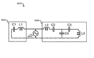
- FIG. 55( a ) is a schematic of an embodiment of a source with two energy transfer elements arranged in parallel and FIG. 55( b ) is a schematic of source with two energy transfer elements arranged in series.
- FIG. 56 is a schematic of an embodiment of a source with two energy transfer elements arranged in parallel.
- FIG. 57 is a schematic of an embodiment of a source with three energy transfer elements arranged in parallel.
- FIG. 58 is a schematic of an embodiment of a source with two energy transfer elements arranged in series.
- FIG. 59 is a schematic of an embodiment of a source with inductively coupled energy transfer elements.
- FIG. 60 is a schematic of an embodiment of an arrangement of energy transfer elements in a source.
- Energy or power may be transferred wirelessly using a variety of techniques.
- Techniques may include induction based contactless energy transfer, wireless non-radiative energy transfer, highly resonant magnetic coupling energy transfer, and/or the like.
- different devices may be configured to receive energy via a specific technique.
- it may be desirable to have an energy source that may support more than one of the techniques allowing energy transfer to a device regardless of the techniques the device is configured for.
- different consumer electronics may be configured to receive energy wirelessly using different energy transfer techniques.
- Older devices for example, may be based on induction based techniques operating at a first frequency while newer more advanced devices may, for example, be configured to receive energy using highly resonant magnetic coupling techniques that may operate at a different frequency.
- a device configured to receive energy via one technique using a specific frequency will not receive energy from a source configured for energy transfer using a different technique based on a different frequency.
- a user would need multiple wireless energy sources configured for each energy transfer technique and frequency to transfer power to the devices.
- Efforts to combine capabilities of different sources based on different techniques into one source typically result in ineffective and/or cost prohibitive designs that replicate hardware (i.e. amplifiers, inverters) for each different technique and/or frequency supported and/or use expensive or lossy switching devices (i.e. transistors, relays) to multiplex and select different components for the various techniques and modes of operation.
- hardware i.e. amplifiers, inverters
- expensive or lossy switching devices i.e. transistors, relays
- a single source may be configured to support multiple energy transfer techniques and/or frequencies.
- a single source may be configured or configurable to support energy transfer to devices designed for energy transfer using different techniques and/or frequencies.
- the embodiments of a source disclosed herein are capable of transferring power using different techniques and/or frequencies with reduced replication of hardware and/or lossy switching devices.
- Non-radiative or near-field wireless energy transfer scheme that is capable of transmitting useful amounts of power over mid-range distances and alignment offsets.
- This inventive technique uses coupled electromagnetic resonators with long-lived oscillatory resonant modes to transfer power from a power supply 4004 to a power drain 4008 .
- the technique is general and may be applied to a wide range of resonators, even where the specific examples disclosed herein relate to electromagnetic resonators. If the resonators are designed such that the energy stored by the electric field is primarily confined within the structure and that the energy stored by the magnetic field is primarily in the region surrounding the resonator. Then, the energy exchange is mediated primarily by the resonant magnetic near-field.
- resonators may be referred to as magnetic resonators. If the resonators are designed such that the energy stored by the magnetic field is primarily confined within the structure and that the energy stored by the electric field is primarily in the region surrounding the resonator. Then, the energy exchange is mediated primarily by the resonant electric near-field. These types of resonators may be referred to as electric resonators. Either type of resonator may also be referred to as an electromagnetic resonator. Both types of resonators are disclosed herein.
- Wireless energy transfer systems may be designed so that the “coupling-time” between resonators is much shorter than the resonators' “loss-times”. Therefore, the systems and methods described herein may utilize high quality factor (high-Q) resonators with low intrinsic-loss rates.
- the systems and methods described herein may use sub-wavelength resonators with near-fields that extend significantly longer than the characteristic sizes of the resonators, so that the near-fields of the resonators that exchange energy overlap at mid-range distances. This is a regime of operation that has not been practiced before and that differs significantly from traditional induction designs.
- wireless energy transfer we may use the terms wireless energy transfer, wireless power transfer, wireless power transmission, and the like, interchangeably.
- intermediate resonators that extend the range of the wireless energy transfer system by allowing energy to hop, transfer through, be temporarily stored, be partially dissipated, or for the transfer to be mediated in any way, from a source resonator to any combination of other device and intermediate resonators, so that energy transfer networks, or strings, or extended paths may be realized.
- Device resonators may receive energy from a source resonator, convert a portion of that energy to electric power for powering or charging a device, and simultaneously pass a portion of the received energy onto other device or mobile device resonators. Energy may be transferred from a source resonator to multiple device resonators, significantly extending the distance over which energy may be wirelessly transferred.
- the wireless power transmission systems may be implemented using a variety of system architectures and resonator designs.
- the systems may include a single source or multiple sources transmitting power to a single device or multiple devices.
- the resonators may be designed to be source or device resonators, or they may be designed to be repeaters. In some cases, a resonator may be a device and source resonator simultaneously, or it may be switched from operating as a source to operating as a device or a repeater.
- One skilled in the art will understand that a variety of system architectures may be supported by the wide range of resonator designs and functionalities described in this application.
- remote devices may be powered directly, using the wirelessly supplied power or energy, or the devices may be coupled to an energy storage unit such as a battery, a super-capacitor, an ultra-capacitor, or the like (or other kind of power drain), where the energy storage unit may be charged or re-charged wirelessly, and/or where the wireless power transfer mechanism is simply supplementary to the main power source of the device.
- the devices may be powered by hybrid battery/energy storage devices such as batteries with integrated storage capacitors and the like.
- novel battery and energy storage devices may be designed to take advantage of the operational improvements enabled by wireless power transmission systems.
- circuit components such as capacitors, inductors, resistors, diodes, switches and the like as circuit components or elements.
- circuit components such as capacitors, inductors, resistors, diodes, switches and the like as circuit components or elements.
- series and parallel combinations of these components as elements, networks, topologies, circuits, and the like.
- combinations of capacitors, diodes, varactors, transistors, and/or switches as adjustable impedance networks, tuning networks, matching networks, adjusting elements, and the like.
- self-resonant objects that have both capacitance, and inductance distributed (or partially distributed, as opposed to solely lumped) throughout the entire object.
- adjusting and controlling variable components within a circuit or network may adjust the performance of that circuit or network and that those adjustments may be described generally as tuning, adjusting, matching, correcting, and the like.
- Other methods to tune or adjust the operating point of the wireless power transfer system may be used alone, or in addition to adjusting tunable components such as inductors and capacitors, or banks of inductors and capacitors.
- a resonator may be defined as a system that can store energy in at least two different forms, and where the stored energy is oscillating between the two forms.
- the resonance has a specific oscillation mode with a resonant (modal) frequency, f, and a resonant (modal) field.
- the energy in the resonator 102 shown in FIG. 1 may decay or be lost by intrinsic losses.
- the resonator fields then obey the following linear equation:
- a(t) is the resonant field amplitude, defined so that the energy contained within the resonator is given by
- ⁇ is the intrinsic energy decay or loss rate (e.g. due to absorption and radiation losses).
- the quality factor also represents the number of oscillation periods, T, it takes for the energy in the resonator to decay by a factor of e.
- FIG. 2 shows an electromagnetic resonator 102 labeled according to this convention. Note that in this figure, there are no extraneous objects or additional resonators in the vicinity of resonator 1 .
- Extraneous objects and/or additional resonators in the vicinity of a first resonator may perturb or load the first resonator, thereby perturbing or loading the Q of the first resonator, depending on a variety of factors such as the distance between the resonator and object or other resonator, the material composition of the object or other resonator, the structure of the first resonator, the power in the first resonator, and the like.
- Unintended external energy losses or coupling mechanisms to extraneous materials and objects in the vicinity of the resonators may be referred to as “perturbing” the Q of a resonator, and may be indicated by a subscript within rounded parentheses, ( ).
- Intended external energy losses, associated with energy transfer via coupling to other resonators and to generators and loads in the wireless energy transfer system may be referred to as “loading” the Q of the resonator, and may be indicated by a subscript within square brackets, [ ].
- the Q of a resonator 102 connected or coupled to a power generator, g, or load 302 , l may be called the “loaded quality factor” or the “loaded Q” and may be denoted by Q [g] or Q [l] , as illustrated in FIG. 3 .
- the “loading quality factor” or the “loading Q” due to a power generator or load connected to the resonator we define the “loading quality factor” or the “loading Q” due to a power generator or load connected to the resonator, as ⁇ Q [l] , where, 1/ ⁇ Q [l] ⁇ 1/Q [l] ⁇ 1/Q. Note that the larger the loading Q, ⁇ Q [l] , of a generator or load, the less the loaded Q, Q [l] , deviates from the unloaded Q of the resonator.
- the Q of a resonator in the presence of an extraneous object 402 , p, that is not intended to be part of the energy transfer system may be called the “perturbed quality factor” or the “perturbed Q” and may be denoted by Q (p) , as illustrated in FIG. 4 .
- Q (p) the Q of a resonator in the presence of an extraneous object 402 , p, that is not intended to be part of the energy transfer system
- Q (p) the “perturbed quality factor”
- Q (p) the Q (p) , as illustrated in FIG. 4 .
- the perturbed Q may be denoted Q (p1+p2+ . . . ) or Q ( ⁇ p ⁇ ) .
- Q 1(brick+wood) may denote the perturbed quality factor of a first resonator in a system for wireless power exchange in the presence of a brick and a piece of wood
- Q 2( ⁇ office ⁇ ) may denote the perturbed quality factor of a second resonator in a system for wireless power exchange in an office environment.
- the perturbing quality factor or the “perturbing Q” due to an extraneous object, p, as ⁇ Q (p) , where 1/ ⁇ Q (p) ⁇ 1/Q (p) ⁇ 1/Q.
- the perturbing quality factor may be due to multiple extraneous objects, p 1 , p 2 , etc. or a set of extraneous objects, ⁇ p ⁇ .
- ⁇ (p) ⁇ Q (p) /Q we also define ⁇ (p) ⁇ Q (p) /Q and call it the “quality factor insensitivity” or the “Q-insensitivity” of the resonator in the presence of an extraneous object.
- a subscript index, such as ⁇ 1(p) indicates the resonator to which the perturbed and unperturbed quality factors are referring, namely, ⁇ 1(p) ⁇ Q 1(p) /Q 1 .
- the quality factor, Q may also be characterized as “unperturbed”, when necessary to distinguish it from the perturbed quality factor, Q (p) , and “unloaded”, when necessary to distinguish it from the loaded quality factor, Q [ ].
- the perturbed quality factor, Q (p) may also be characterized as “unloaded”, when necessary to distinguish them from the loaded perturbed quality factor, Q (p)[l] .
- Resonators having substantially the same resonant frequency, coupled through any portion of their near-fields may interact and exchange energy.
- One way to describe and model the energy exchange between two coupled resonators is using coupled mode theory (CMT).
- CMT coupled mode theory
- d a m ⁇ ( t ) d t - i ⁇ ( ⁇ m - i ⁇ m ) ⁇ a m ⁇ ( t ) + i ⁇ ⁇ n ⁇ m ⁇ ⁇ ⁇ mn ⁇ a n ⁇ ( t )
- U mn strong-coupling factor
- the quality factor of a resonator m in the presence of a similar frequency resonator n or additional resonators, may be loaded by that resonator n or additional resonators, in a fashion similar to the resonator being loaded by a connected power generating or consuming device.
- the fact that resonator m may be loaded by resonator n and vice versa is simply a different way to see that the resonators are coupled.
- the loaded Q's of the resonators in these cases may be denoted as Q m[n] and Q n[m] .
- the total loading of a resonator may be determined by modeling each load as a resistive loss, and adding the multiple loads in the appropriate parallel and/or series combination to determine the equivalent load of the ensemble.
- the “loading quality factor” or the “loading Q m ” of resonator m due to resonator n as ⁇ Q m[n] , where 1/ ⁇ Q m[n] ⁇ 1/Q m[n] ⁇ 1/Q m .
- resonator n is also loaded by resonator m and its “loading Q n ” is given by 1/ ⁇ Q n[m] ⁇ 1/Q n[m] ⁇ 1/Q n .
- s +m (t) and s ⁇ m (t) are respectively the amplitudes of the fields coming from a generator into the resonator m and going out of the resonator m either back towards the generator or into a load, defined so that the power they carry is given by
- the loading coefficients ⁇ m relate to the rate at which energy is exchanged between the resonator m and the generator or load connected to it.
- FIG. 1( a ) shows an example of two coupled resonators 1000 , a first resonator 102 S, configured as a source resonator and a second resonator 102 D, configured as a device resonator.
- Energy may be transferred over a distance D between the resonators.
- the source resonator 102 S may be driven by a power supply or generator (not shown).
- Work may be extracted from the device resonator 102 D by a power consuming drain or load (e.g. a load resistor, not shown).
- the efficiency, ⁇
- 2 of the power transmission from the generator to the load (via the source and device resonators) is maximized under the following conditions:
- the coupling efficiency, ⁇ is greater than 1% when U is greater than 0.2, is greater than 10% when U is greater than 0.7, is greater than 17% when U is greater than 1, is greater than 52% when U is greater than 3, is greater than 80% when U is greater than 9, is greater than 90% when U is greater than 19, and is greater than 95% when U is greater than 45.
- the regime of operation where U>1 may be referred to as the “strong-coupling” regime.
- resonators may be used that are high-Q.
- the Q of each resonator may be high.
- the geometric mean of the resonator Q's, ⁇ square root over (Q s Q d ) ⁇ may also or instead be high.
- the coupling factor, k is a number between 0 ⁇ k ⁇ 1, and it may be independent (or nearly independent) of the resonant frequencies of the source and device resonators, rather it may be determined mostly by their relative geometry and the physical decay-law of the field mediating their coupling.
- the resonant frequencies of the resonators may be chosen preferably to achieve a high Q rather than to achieve a low , as these two goals may be achievable at two separate resonant frequency regimes.
- a high-Q resonator may be defined as one with Q>100.
- Two coupled resonators may be referred to as a system of high-Q resonators when each resonator has a Q greater than 100, Q s >100 and Q d >100.
- two coupled resonators may be referred to as a system of high-Q resonators when the geometric mean of the resonator Q's is greater than 100, ⁇ square root over (Q s Q d ) ⁇ >100.
- the resonators may be named or numbered. They may be referred to as source resonators, device resonators, first resonators, second resonators, repeater resonators, and the like. It is to be understood that while two resonators are shown in FIG. 1 , and in many of the examples below, other implementations may include three (3) or more resonators.
- a single source resonator 102 S may transfer energy to multiple device resonators 102 D or multiple devices. Energy may be transferred from a first device to a second, and then from the second device to the third, and so forth.
- Multiple sources may transfer energy to a single device or to multiple devices connected to a single device resonator or to multiple devices connected to multiple device resonators.
- Resonators 102 may serve alternately or simultaneously as sources, devices, or they may be used to relay power from a source in one location to a device in another location. Intermediate electromagnetic resonators 102 may be used to extend the distance range of wireless energy transfer systems. Multiple resonators 102 may be daisy chained together, exchanging energy over extended distances and with a wide range of sources and devices. High power levels may be split between multiple sources 102 S, transferred to multiple devices and recombined at a distant location.
- the analysis of a single source and a single device resonator may be extended to multiple source resonators and/or multiple device resonators and/or multiple intermediate resonators.
- the conclusion may be that large strong-coupling factors, U mn , between at least some or all of the multiple resonators is preferred for a high system efficiency in the wireless energy transfer.
- implementations may use source, device and intermediate resonators that have a high Q.
- the Q of each resonator may be high.
- the geometric mean ⁇ square root over (Q m Q n ) ⁇ of the Q's for pairs of resonators m and n, for which a large U mn is desired, may also or instead be high.
- the strong-coupling factor of two resonators may be determined by the relative magnitudes of the loss mechanisms of each resonator and the coupling mechanism between the two resonators, the strength of any or all of these mechanisms may be perturbed in the presence of extraneous objects in the vicinity of the resonators as described above.
- k the coupling factor in the absence of extraneous objects or materials.
- k (p) the coupling factor in the presence of an extraneous object
- k (p) the coupling factor in the presence of an extraneous object
- the coupling factor, k may also be characterized as “unperturbed”, when necessary to distinguish from the perturbed coupling factor k (p) .
- ⁇ (p) ⁇ k (p) /k we call it the “coupling factor insensitivity” or the “k-insensitivity”.
- Lower indices, such as ⁇ 12(p) indicate the resonators to which the perturbed and unperturbed coupling factor is referred to, namely ⁇ 12(p) ⁇ k 12(p) /k 12 .
- U the strong-coupling factor in the absence of extraneous objects.
- U (p) U (p) )
- U (p) k (p) ⁇ square root over (Q 1(p) Q 2(p) ) ⁇
- the strong-coupling factor U may also be characterized as “unperturbed”, when necessary to distinguish from the perturbed strong-coupling factor U (p) .
- the strong-coupling factor U may also be characterized as “unperturbed”, when necessary to distinguish from the perturbed strong-coupling factor U (p) .
- ⁇ (p) ⁇ U (p) /U we also define ⁇ (p) ⁇ U (p) /U and call it the “strong-coupling factor insensitivity” or the “U-insensitivity”.
- Lower indices, such as ⁇ 12(p) indicate the resonators to which the perturbed and unperturbed coupling factor refers, namely ⁇ 12(p) ⁇ U 12(p) /U 12 .
- the efficiency of the energy exchange in a perturbed system may be given by the same formula giving the efficiency of the unperturbed system, where all parameters such as strong-coupling factors, coupling factors, and quality factors are replaced by their perturbed equivalents.
- Source, device and/or intermediate resonators may have a high Q (p) .
- the so-called “useful” energy in a useful energy exchange is the energy or power that must be delivered to a device (or devices) in order to power or charge the device.
- the transfer efficiency that corresponds to a useful energy exchange may be system or application dependent. For example, high power vehicle charging applications that transfer kilowatts of power may need to be at least 80% efficient in order to supply useful amounts of power resulting in a useful energy exchange sufficient to recharge a vehicle battery, without significantly heating up various components of the transfer system.
- a useful energy exchange may include any energy transfer efficiencies greater than 10%, or any other amount acceptable to keep rechargeable batteries “topped off” and running for long periods of time.
- transfer efficiencies that are much less than 1% may be adequate for powering multiple low power sensors from a single source located a significant distance from the sensors.
- transfer efficiencies may be acceptable for a useful energy exchange and may be said to supply useful power to devices in those applications.
- an operating distance is any distance over which a useful energy exchange is or can be maintained according to the principles disclosed herein.
- a useful energy exchange for a wireless energy transfer in a powering or recharging application may be efficient, highly efficient, or efficient enough, as long as the wasted energy levels, heat dissipation, and associated field strengths are within tolerable limits.
- the tolerable limits may depend on the application, the environment and the system location.
- Wireless energy transfer for powering or recharging applications may be efficient, highly efficient, or efficient enough, as long as the desired system performance may be attained for the reasonable cost restrictions, weight restrictions, size restrictions, and the like.
- Efficient energy transfer may be determined relative to that which could be achieved using traditional inductive techniques that are not high-Q systems. Then, the energy transfer may be defined as being efficient, highly efficient, or efficient enough, if more energy is delivered than could be delivered by similarly sized coil structures in traditional inductive schemes over similar distances or alignment offsets.
- Efficient energy exchange may be realized so long as the relative offset of the resonant frequencies (
- the Q matching condition may be less critical than the frequency matching condition for efficient energy exchange.
- the degree by which the strong-loading factors, U m[l] , of the resonators due to generators and/or loads may be away from their optimal values and still have efficient enough energy exchange depends on the particular system, whether all or some of the generators and/or loads are Q-mismatched and so on.
- the resonant frequencies of the resonators may not be exactly matched, but may be matched within the above tolerances.
- the strong-loading factors of at least some of the resonators due to generators and/or loads may not be exactly matched to their optimal value.
- the voltage levels, current levels, impedance values, material parameters, and the like may not be at the exact values described in the disclosure but will be within some acceptable tolerance of those values.
- the system optimization may include cost, size, weight, complexity, and the like, considerations, in addition to efficiency, Q, frequency, strong coupling factor, and the like, considerations. Some system performance parameters, specifications, and designs may be far from optimal in order to optimize other system performance parameters, specifications and designs.
- At least some of the system parameters may be varying in time, for example because components, such as sources or devices, may be mobile or aging or because the loads may be variable or because the perturbations or the environmental conditions are changing etc. In these cases, in order to achieve acceptable matching conditions, at least some of the system parameters may need to be dynamically adjustable or tunable. All the system parameters may be dynamically adjustable or tunable to achieve approximately the optimal operating conditions. However, based on the discussion above, efficient enough energy exchange may be realized even if some system parameters are not variable.
- at least some of the devices may not be dynamically adjusted.
- at least some of the sources may not be dynamically adjusted.
- at least some of the intermediate resonators may not be dynamically adjusted. In some examples, none of the system parameters may be dynamically adjusted.
- the resonators used to exchange energy may be electromagnetic resonators.
- the intrinsic energy decay rates, ⁇ m are given by the absorption (or resistive) losses and the radiation losses of the resonator.
- the resonator may be constructed such that the energy stored by the electric field is primarily confined within the structure and that the energy stored by the magnetic field is primarily in the region surrounding the resonator. Then, the energy exchange is mediated primarily by the resonant magnetic near-field.
- These types of resonators may be referred to as magnetic resonators.
- the resonator may be constructed such that the energy stored by the magnetic field is primarily confined within the structure and that the energy stored by the electric field is primarily in the region surrounding the resonator. Then, the energy exchange is mediated primarily by the resonant electric near-field.
- These types of resonators may be referred to as electric resonators.
- the total electric and magnetic energies stored by the resonator have to be equal, but their localizations may be quite different.
- the ratio of the average electric field energy to the average magnetic field energy specified at a distance from a resonator may be used to characterize or describe the resonator.
- Electromagnetic resonators may include an inductive element, a distributed inductance, or a combination of inductances with inductance, L, and a capacitive element, a distributed capacitance, or a combination of capacitances, with capacitance, C.
- a minimal circuit model of an electromagnetic resonator 102 is shown in FIG. 6 a .
- the resonator may include an inductive element 108 and a capacitive element 104 .
- initial energy such as electric field energy stored in the capacitor 104
- the system will oscillate as the capacitor discharges transferring energy into magnetic field energy stored in the inductor 108 which in turn transfers energy back into electric field energy stored in the capacitor 104 .
- the resonators 102 shown in FIGS. 6( b )( c )( d ) may be referred to as magnetic resonators.
- Magnetic resonators may be preferred for wireless energy transfer applications in populated environments because most everyday materials including animals, plants, and humans are non-magnetic (i.e., ⁇ / ⁇ 1), so their interaction with magnetic fields is minimal and due primarily to eddy currents induced by the time-variation of the magnetic fields, which is a second-order effect. This characteristic is important both for safety reasons and because it reduces the potential for interactions with extraneous environmental objects and materials that could alter system performance.
- FIG. 6 d shows a simplified drawing of some of the electric and magnetic field lines associated with an exemplary magnetic resonator 102 B.
- the magnetic resonator 102 B may include a loop of conductor acting as an inductive element 108 and a capacitive element 104 at the ends of the conductor loop. Note that this drawing depicts most of the energy in the region surrounding the resonator being stored in the magnetic field, and most of the energy in the resonator (between the capacitor plates) stored in the electric field.
- Some electric field owing to fringing fields, free charges, and the time varying magnetic field, may be stored in the region around the resonator, but the magnetic resonator may be designed to confine the electric fields to be close to or within the resonator itself, as much as possible.
- the inductor 108 and capacitor 104 of an electromagnetic resonator 102 may be bulk circuit elements, or the inductance and capacitance may be distributed and may result from the way the conductors are formed, shaped, or positioned, in the structure.
- the inductor 108 may be realized by shaping a conductor to enclose a surface area, as shown in FIGS. 6( b )( c )( d ) .
- This type of resonator 102 may be referred to as a capacitively-loaded loop inductor. Note that we may use the terms “loop” or “coil” to indicate generally a conducting structure (wire, tube, strip, etc.), enclosing a surface of any shape and dimension, with any number of turns.
- the enclosed surface area is circular, but the surface may be any of a wide variety of other shapes and sizes and may be designed to achieve certain system performance specifications.
- the inductance for a length of circular conductor arranged to form a circular single-turn loop is approximately,
- ⁇ 0 is the magnetic permeability of free space
- x is the radius of the enclosed circular surface area
- a is the radius of the conductor used to form the inductor loop.
- the inductance for other cross-section conductors, arranged to form other enclosed surface shapes, areas, sizes, and the like, and of any number of wire turns, may be calculated analytically, numerically or it may be determined by measurement.
- the inductance may be realized using inductor elements, distributed inductance, networks, arrays, series and parallel combinations of inductors and inductances, and the like.
- the inductance may be fixed or variable and may be used to vary impedance matching as well as resonant frequency operating conditions.
- Capacitor plates 110 may be formed and utilized as shown in FIG. 6 b , or the capacitance may be distributed and be realized between adjacent windings of a multi-loop conductor 114 , as shown in FIG. 6 c .
- the capacitance may be realized using capacitor elements, distributed capacitance, networks, arrays, series and parallel combinations of capacitances, and the like.
- the capacitance may be fixed or variable and may be used to vary impedance matching as well as resonant frequency operating conditions.
- inductance and capacitance in an electromagnetic resonator 102 may be lumped, distributed, or a combination of lumped and distributed inductance and capacitance and that electromagnetic resonators may be realized by combinations of the various elements, techniques and effects described herein.
- Electromagnetic resonators 102 may be include inductors, inductances, capacitors, capacitances, as well as additional circuit elements such as resistors, diodes, switches, amplifiers, diodes, transistors, transformers, conductors, connectors and the like.
- the resonant frequency of the resonator may be changed by tuning the inductance, L, and/or the capacitance, C, of the resonator.
- the resonator frequency may be design to operate at the so-called ISM (Industrial, Scientific and Medical) frequencies as specified by the FCC.
- the resonator frequency may be chosen to meet certain field limit specifications, specific absorption rate (SAR) limit specifications, electromagnetic compatibility (EMC) specifications, electromagnetic interference (EMI) specifications, component size, cost or performance specifications, and the like.
- the energy in the resonators 102 shown in FIG. 6 may decay or be lost by intrinsic losses including absorptive losses (also called ohmic or resistive losses) and/or radiative losses.
- the Quality Factor, or Q, of the resonator which characterizes the energy decay, is inversely proportional to these losses. Absorptive losses may be caused by the finite conductivity of the conductor used to form the inductor as well as by losses in other elements, components, connectors, and the like, in the resonator.
- An inductor formed from low loss materials may be referred to as a “high-Q inductive element” and elements, components, connectors and the like with low losses may be referred to as having “high resistive Q's”.
- the total absorptive loss for a resonator may be calculated as the appropriate series and/or parallel combination of resistive losses for the various elements and components that make up the resonator. That is, in the absence of any significant radiative or component/connection losses, the Q of the resonator may be given by, Q abs ,
- the cross-sectional area over which current flows may be less than the physical cross-sectional area of the conductor owing to the skin effect. Therefore, high-Q magnetic resonators may be composed of conductors with high conductivity, relatively large surface areas and/or with specially designed profiles (e.g. Litz wire) to minimize proximity effects and reduce the AC resistance.
- the magnetic resonator structures may include high-Q inductive elements composed of high conductivity wire, coated wire, Litz wire, ribbon, strapping or plates, tubing, paint, gels, traces, and the like.
- the magnetic resonators may be self-resonant, or they may include external coupled elements such as capacitors, inductors, switches, diodes, transistors, transformers, and the like.
- the magnetic resonators may include distributed and lumped capacitance and inductance. In general, the Q of the resonators will be determined by the Q's of all the individual components of the resonator.
- resonators may be designed to increase L, within certain other constraints.
- One way to increase L is to use more than one turn of the conductor to form the inductor in the resonator. Design techniques and trade-offs may depend on the application, and a wide variety of structures, conductors, components, and resonant frequencies may be chosen in the design of high-Q magnetic resonators.
- the size of the magnetic resonator may be much less than the wavelength of operation so radiation losses may be very small. Such structures may be referred to as sub-wavelength resonators. Radiation may be a loss mechanism for non-radiative wireless energy transfer systems and designs may be chosen to reduce or minimize R rad . Note that a high-Q rad may be desirable for non-radiative wireless energy transfer schemes.
- resonators for non-radiative wireless energy transfer differs from antennas designed for communication or far-field energy transmission purposes.
- capacitively-loaded conductive loops may be used as resonant antennas (for example in cell phones), but those operate in the far-field regime where the radiation Q's are intentionally designed to be small to make the antenna efficient at radiating energy.
- Such designs are not appropriate for the efficient near-field wireless energy transfer technique disclosed in this application.
- FIG. 7 shows a plot of Q of an exemplary magnetic resonator (in this case a coil with a diameter of 60 cm made of copper pipe with an outside diameter (OD) of 4 cm) that may be used for wireless power transmission at MHz frequencies.
- the absorptive Q (dashed line) 702 increases with frequency, while the radiative Q (dotted line) 704 decreases with frequency, thus leading the overall Q to peak 708 at a particular frequency.
- the Q of this exemplary resonator is greater than 100 over a wide frequency range.
- Magnetic resonators may be designed to have high-Q over a range of frequencies and system operating frequency may set to any frequency in that range.
- the Q may be defined using the intrinsic decay rate, 2 ⁇ , as described previously.
- the intrinsic decay rate is the rate at which an uncoupled and undriven resonator loses energy.
- Q mechanism a quality factor related only to a specific loss mechanism
- Q 1,mechanism a quality factor related only to a specific loss mechanism
- Q 1,rad the quality factor for resonator 1 related to its radiation losses.
- the high-Q electromagnetic resonators used in the near-field wireless energy transfer system disclosed here may be sub-wavelength objects. That is, the physical dimensions of the resonator may be much smaller than the wavelength corresponding to the resonant frequency.
- Sub-wavelength magnetic resonators may have most of the energy in the region surrounding the resonator stored in their magnetic near-fields, and these fields may also be described as stationary or non-propagating because they do not radiate away from the resonator.
- the extent of the near-field in the area surrounding the resonator is typically set by the wavelength, so it may extend well beyond the resonator itself for a sub-wavelength resonator.
- the limiting surface, where the field behavior changes from near-field behavior to far-field behavior may be called the “radiation caustic”.
- the strength of the near-field is reduced the farther one gets away from the resonator. While the field strength of the resonator near-fields decays away from the resonator, the fields may still interact with objects brought into the general vicinity of the resonator. The degree to which the fields interact depends on a variety of factors, some of which may be controlled and designed, and some of which may not.
- the wireless energy transfer schemes described herein may be realized when the distance between coupled resonators is such that one resonator lies within the radiation caustic of the other.
- the near-field profiles of the electromagnetic resonators may be similar to those commonly associated with dipole resonators or oscillators. Such field profiles may be described as omni-directional, meaning the magnitudes of the fields are non-zero in all directions away from the object.
- Spatially separated and/or offset magnetic resonators of sufficient Q may achieve efficient wireless energy transfer over distances that are much larger than have been seen in the prior art, even if the sizes and shapes of the resonator structures are different. Such resonators may also be operated to achieve more efficient energy transfer than was achievable with previous techniques over shorter range distances. We describe such resonators as being capable of mid-range energy transfer.
- Mid-range distances may be defined as distances that are larger than the characteristic dimension of the smallest of the resonators involved in the transfer, where the distance is measured from the center of one resonator structure to the center of a spatially separated second resonator structure.
- two-dimensional resonators are spatially separated when the areas circumscribed by their inductive elements do not intersect and three-dimensional resonators are spatially separated when their volumes do not intersect.
- a two-dimensional resonator is spatially separated from a three-dimensional resonator when the area circumscribed by the former is outside the volume of the latter.
- FIG. 8 shows some example resonators with their characteristic dimensions labeled.
- the characteristic sizes 802 of resonators 102 may be defined in terms of the size of the conductor and the area circumscribed or enclosed by the inductive element in a magnetic resonator and the length of the conductor forming the capacitive element of an electric resonator. Then, the characteristic size 802 of a resonator 102 , x char , may be equal to the radius of the smallest sphere that can fit around the inductive or capacitive element of the magnetic or electric resonator respectively, and the center of the resonator structure is the center of the sphere.
- the characteristic thickness 804 , t char , of a resonator 102 may be the smallest possible height of the highest point of the inductive or capacitive element in the magnetic or capacitive resonator respectively, measured from a flat surface on which it is placed.
- the characteristic width 808 of a resonator 102 , w char may be the radius of the smallest possible circle through which the inductive or capacitive element of the magnetic or electric resonator respectively, may pass while traveling in a straight line.
- the characteristic width 808 of a cylindrical resonator may be the radius of the cylinder.
- the efficiency of the energy exchange between two resonators may depend on the relative position and orientation of the resonators. That is, the efficiency of the energy exchange may be maximized for particular relative orientations of the resonators.
- the sensitivity of the transfer efficiency to the relative position and orientation of two uncompensated resonators may be captured in the calculation of either k or ⁇ . While coupling may be achieved between resonators that are offset and/or rotated relative to each other, the efficiency of the exchange may depend on the details of the positioning and on any feedback, tuning, and compensation techniques implemented during operation.
- the inductance, L, for such a N-turn loop is approximately N 2 times the inductance of a single-turn loop given previously.
- the quality factor of such a resonator, Q ⁇ L/(R abs +R rad ), is highest for a particular frequency determined by the system parameters ( FIG. 4 ). As described previously, at lower frequencies the Q is determined primarily by absorption losses and at higher frequencies the Q is determined primarily by radiation losses.
- the absorptive losses may be minimized by using low loss conductors to form the inductive elements.
- the loss of the conductors may be minimized by using large surface area conductors such as conductive tubing, strapping, strips, machined objects, plates, and the like, by using specially designed conductors such as Litz wire, braided wires, wires of any cross-section, and other conductors with low proximity losses, in which case the frequency scaled behavior described above may be different, and by using low resistivity materials such as high-purity copper and silver, for example.
- One advantage of using conductive tubing as the conductor at higher operating frequencies is that it may be cheaper and lighter than a similar diameter solid conductor, and may have similar resistance because most of the current is traveling along the outer surface of the conductor owing to the skin effect.
- the rate for energy transfer between two resonators of characteristic size x 1 and x 2 , and separated by a distance D between their centers, may be given by ⁇ .
- D/x 10, 8, 6.
- ⁇ /2 ⁇ 3033, 1553, 655 respectively.
- the corresponding coupling-to-loss ratios peak at the frequency where the inductive element Q peaks and are ⁇ / ⁇ 0.4, 0.79, 1.97 and 0.15, 0.3, 0.72 and 0.2, 0.4, 0.94 for the three inductive element sizes and distances described above.
- the optimal system operating frequency lies between the peaks of the individual resonator Q's.
- Inductive elements may be formed for use in high-Q magnetic resonators.
- Inductive elements may be formed using a variety of conductors arranged in a variety of shapes, enclosing any size or shaped area, and they may be single turn or multiple turn elements. Drawings of exemplary inductive elements 900 A-B are shown in FIG. 9 .
- the inductive elements may be formed to enclose a circle, a rectangle, a square, a triangle, a shape with rounded corners, a shape that follows the contour of a particular structure or device, a shape that follows, fills, or utilizes, a dedicated space within a structure or device, and the like.
- the designs may be optimized for size, cost, weight, appearance, performance, and the like.
- conductors may be bent or formed into the desired size, shape, and number of turns. However, it may be difficult to accurately reproduce conductor shapes and sizes using manual techniques. In addition, it may be difficult to maintain uniform or desired center-to-center spacings between the conductor segments in adjacent turns of the inductive elements. Accurate or uniform spacing may be important in determining the self-capacitance of the structure as well as any proximity effect induced increases in AC resistance, for example.
- Molds may be used to replicate inductor elements for high-Q resonator designs.
- molds may be used to accurately shape conductors into any kind of shape without creating kinks, buckles or other potentially deleterious effects in the conductor.
- Molds may be used to form the inductor elements and then the inductor elements may be removed from the forms. Once removed, these inductive elements may be built into enclosures or devices that may house the high-Q magnetic resonator. The formed elements may also or instead remain in the mold used to form them.
- the molds may be formed using standard CNC (computer numerical control) routing or milling tools or any other known techniques for cutting or forming grooves in blocks.
- the molds may also or instead be formed using machining techniques, injection molding techniques, casting techniques, pouring techniques, vacuum techniques, thermoforming techniques, cut-in-place techniques, compression forming techniques and the like.
- the formed element may be removed from the mold or it may remain in the mold.
- the mold may be altered with the inductive element inside.
- the mold may be covered, machined, attached, painted and the like.
- the mold and conductor combination may be integrated into another housing, structure or device.
- the grooves cut into the molds may be any dimension and may be designed to form conducting tubing, wire, strapping, strips, blocks, and the like into the desired inductor shapes and sizes.
- the inductive elements used in magnetic resonators may contain more than one loop and may spiral inward or outward or up or down or in some combination of directions.
- the magnetic resonators may have a variety of shapes, sizes and number of turns and they may be composed of a variety of conducing materials.
- the magnetic resonators may be free standing or they may be enclosed in an enclosure, container, sleeve or housing.
- the magnetic resonators may include the form used to make the inductive element.
- These various forms and enclosures may be composed of almost any kind of material. Low loss materials such as Teflon, REXOLITE, styrene, and the like may be preferable for some applications.
- These enclosures may contain fixtures that hold the inductive elements.
- Magnetic resonators may be composed of self-resonant coils of copper wire or copper tubing.
- a magnetic resonator structure may be configured so that x is about 30 cm, his about 20 cm, a is about 3 mm and N is about 5.25, and, during operation, a power source coupled to the magnetic resonator may drive the resonator at a resonant frequency, f, where f is about 10.6 MHz.
- a power source coupled to the magnetic resonator may drive the resonator at a resonant frequency, f, where f is about 10.6 MHz.
- x is about 30 cm, his about 20 cm, a is about 1 cm and N is about 4
- the resonator may be driven at a frequency, f, where f is about 13.4 MHz.
- x is about 10 cm, h is about 3 cm, a is about 2 mm and N is about 6, the resonator may be driven at a frequency, f, where f is about 21.4 MHz.
- High-Q inductive elements may be designed using printed circuit board traces.
- Printed circuit board traces may have a variety of advantages compared to mechanically formed inductive elements including that they may be accurately reproduced and easily integrated using established printed circuit board fabrication techniques, that their AC resistance may be lowered using custom designed conductor traces, and that the cost of mass-producing them may be significantly reduced.
- High-Q inductive elements may be fabricated using standard PCB techniques on any PCB material such as FR-4 (epoxy E-glass), multi-functional epoxy, high performance epoxy, bismalaimide triazine/epoxy, polyimide, Cyanate Ester, polytetraflouroethylene (Teflon), FR-2, FR-3, CEM-1, CEM-2, Rogers, Resolute, and the like.
- the conductor traces may be formed on printed circuit board materials with lower loss tangents.
- the conducting traces may be composed of copper, silver, gold, aluminum, nickel and the like, and they may be composed of paints, inks, or other cured materials.
- the circuit board may be flexible and it may be a flex-circuit.
- the conducting traces may be formed by chemical deposition, etching, lithography, spray deposition, cutting, and the like.
- the conducting traces may be applied to form the desired patterns and they may be formed using crystal and structure growth techniques.
- the dimensions of the conducting traces, as well as the number of layers containing conducting traces, the position, size and shape of those traces and the architecture for interconnecting them may be designed to achieve or optimize certain system specifications such as resonator Q, Q (p) , resonator size, resonator material and fabrication costs, U, U (p) , and the like.
- a three-turn high-Q inductive element 1001 A was fabricated on a four-layer printed circuit board using the rectangular copper trace pattern as shown in FIG. 10( a ) .
- the copper trace is shown in black and the PCB in white.
- the width and thickness of the copper traces in this example was approximately 1 cm (400 mils) and 43 ⁇ m (1.7 mils) respectively.
- the edge-to-edge spacing between turns of the conducting trace on a single layer was approximately 0.75 cm (300 mils) and each board layer thickness was approximately 100 ⁇ m (4 mils).
- the pattern shown in FIG. 10( a ) was repeated on each layer of the board and the conductors were connected in parallel.
- the outer dimensions of the 3-loop structure were approximately 30 cm by 20 cm.
- the measured inductance of this PCB loop was 5.3 ⁇ H.
- a magnetic resonator using this inductor element and tunable capacitors had a quality factor, Q, of 550 at its designed resonance frequency of 6.78 MHz.
- the resonant frequency could be tuned by changing the inductance and capacitance values in the magnetic resonator.
- a two-turn inductor 1001 B was fabricated on a four-layer printed circuit board using the rectangular copper trace pattern shown in FIG. 10( b ) .
- the copper trace is shown in black and the PCB in white.
- the width and height of the copper traces in this example were approximately 0.75 cm (300 mils) and 43 ⁇ m (1.7 mils) respectively.
- the edge-to-edge spacing between turns of the conducting trace on a single layer was approximately 0.635 cm (250 mils) and each board layer thickness was approximately 100 ⁇ m (4 mils).
- the pattern shown in FIG. 10( b ) was repeated on each layer of the board and the conductors were connected in parallel.
- the outer dimensions of the two-loop structure were approximately 7.62 cm by 26.7 cm.
- the measured inductance of this PCB loop was 1.3 ⁇ H.
- Stacking two boards together with a vertical separation of approximately 0.635 cm (250 mils) and connecting the two boards in series produced a PCB inductor with an inductance of approximately 3.4 ⁇ H.
- a magnetic resonator using this stacked inductor loop and tunable capacitors had a quality factor, Q, of 390 at its designed resonance frequency of 6.78 MHz. The resonant frequency could be tuned by changing the inductance and capacitance values in the magnetic resonator.
- the inductive elements may be formed using magnetic materials of any size, shape thickness, and the like, and of materials with a wide range of permeability and loss values. These magnetic materials may be solid blocks, they may enclose hollow volumes, they may be formed from many smaller pieces of magnetic material tiled and or stacked together, and they may be integrated with conducting sheets or enclosures made from highly conducting materials. Wires may be wrapped around the magnetic materials to generate the magnetic near-field. These wires may be wrapped around one or more than one axis of the structure. Multiple wires may be wrapped around the magnetic materials and combined in parallel, or in series, or via a switch to form customized near-field patterns.
- the magnetic resonator may include 15 turns of Litz wire wound around a 19.2 cm ⁇ 10 cm ⁇ 5 mm tiled block of 3F3 ferrite material.
- the Litz wire may be wound around the ferrite material in any direction or combination of directions to achieve the desire resonator performance.
- the number of turns of wire, the spacing between the turns, the type of wire, the size and shape of the magnetic materials and the type of magnetic material are all design parameters that may be varied or optimized for different application scenarios.
- magnetic materials assembled to form an open magnetic circuit albeit one with an air gap on the order of the size of the whole structure, to realize a magnetic resonator structure.
- high conductivity materials are wound around a structure made from magnetic material to form the inductive element of the magnetic resonator.
- Capacitive elements may be connected to the high conductivity materials, with the resonant frequency then determined as described above.
- These magnetic resonators have their dipole moment in the plane of the two dimensional resonator structures, rather than perpendicular to it, as is the case for the capacitively-loaded inductor loop resonators.
- FIG. 11( a ) A diagram of a single planar resonator structure is shown in FIG. 11( a ) .
- the planar resonator structure is constructed of a core of magnetic material 1121 , such as ferrite with a loop or loops of conducting material 1122 wrapped around the core 1121 .
- the structure may be used as the source resonator that transfers power and the device resonator that captures energy.
- the ends of the conductor When used as a source, the ends of the conductor may be coupled to a power source. Alternating electrical current flowing through the conductor loops excites alternating magnetic fields.
- the ends of the conductor may be coupled to a power drain or load.
- FIG. 11( a ) Changing magnetic fields induce an electromotive force in the loop or loops of the conductor wound around the core magnetic material.
- the dipole moment of these types of structures is in the plane of the structures and is, for example, directed along the Y axis for the structure in FIG. 11( a ) .
- Two such structures have strong coupling when placed substantially in the same plane (i.e. the X,Y plane of FIG. 11 ).
- the structures of FIG. 11( a ) have the most favorable orientation when the resonators are aligned in the same plane along their Y axis.
- the geometry and the coupling orientations of the described planar resonators may be preferable for some applications.
- the planar or flat resonator shape may be easier to integrate into many electronic devices that are relatively flat and planar.
- the planar resonators may be integrated into the whole back or side of a device without requiring a change in geometry of the device. Due to the flat shape of many devices, the natural position of the devices when placed on a surface is to lay with their largest dimension being parallel to the surface they are placed on.
- a planar resonator integrated into a flat device is naturally parallel to the plane of the surface and is in a favorable coupling orientation relative to the resonators of other devices or planar resonator sources placed on a flat surface.
- the geometry of the planar resonators may allow easier integration into devices. Their low profile may allow a resonator to be integrated into or as part of a complete side of a device. When a whole side of a device is covered by the resonator, magnetic flux can flow through the resonator core without being obstructed by lossy material that may be part of the device or device circuitry.
- the core of the planar resonator structure may be of a variety of shapes and thicknesses and may be flat or planar such that the minimum dimension does not exceed 30% of the largest dimension of the structure.
- the core may have complex geometries and may have indentations, notches, ridges, and the like. Geometric enhancements may be used to reduce the coupling dependence on orientation and they may be used to facilitate integration into devices, packaging, packages, enclosures, covers, skins, and the like. Two exemplary variations of core geometries are shown in FIG. 11( b ) .
- the planar core 1131 may be shaped such that the ends are substantially wider than the middle of the structure to create an indentation for the conductor winding.
- the core material may be of varying thickness with ends that are thicker and wider than the middle.
- the core material 1132 may have any number of notches or cutouts 1133 of various depths, width, and shapes to accommodate conductor loops, housing, packaging, and the like.
- the shape and dimensions of the core may be further dictated by the dimensions and characteristics of the device that they are integrated into.
- the core material may curve to follow the contours of the device, or may require non-symmetric notches or cutouts to allow clearance for parts of the device.
- the core structure may be a single monolithic piece of magnetic material or may be composed of a plurality of tiles, blocks, or pieces that are arranged together to form the larger structure.
- the different layers, tiles, blocks, or pieces of the structure may be of similar or may be of different materials. It may be desirable to use materials with different magnetic permeability in different locations of the structure. Core structures with different magnetic permeability may be useful for guiding the magnetic flux, improving coupling, and affecting the shape or extent of the active area of a system.
- the conductor of the planar resonator structure may be wound at least once around the core 1141 , 1142 , as shown in FIG. 11( c ) . In certain circumstances, it may be preferred to wind at least three loops.
- the conductor can be any good conductor including conducting wire, Litz wire, conducting tubing, sheets, strips, gels, inks, traces and the like.
- the size, shape, or dimensions of the active area of source may be further enhanced, altered, or modified with the use of materials that block, shield, or guide magnetic fields.
- a magnetic shield to reduce the strength of the magnetic fields in a specific direction.
- the shield may be a conductor or a layered combination of conductor and magnetic material which can be used to guide magnetic fields away from a specific direction. Structures composed of layers of conductors and magnetic materials may be used to reduce energy losses that may occur due to shielding of the source.
- the plurality of planar resonators may be integrated or combined into one planar resonator structure.
- a conductor or conductors may be wound around a core structure such that the loops formed by the two conductors are not coaxial.
- An example of such a structure is shown in FIG. 12 where two conductors 1201 , 1202 are wrapped around a planar rectangular core 1203 at orthogonal angles.
- the core may be rectangular or it may have various geometries with several extensions or protrusions.
- the protrusions may be useful for wrapping of a conductor, reducing the weight, size, or mass of the core, or may be used to enhance the directionality or omni-directionality of the resonator.
- a multi wrapped planar resonator with four protrusions is shown by the inner structure 1310 in FIG. 13 , where four conductors 1301 , 1302 , 1303 , 1304 are wrapped around the core.
- the core may have extensions 1305 , 1306 , 1307 , 1308 with one or more conductor loops.
- a single conductor may be wrapped around a core to form loops that are not coaxial.
- the four conductor loops of FIG. 13 for example, may be formed with one continuous piece of conductor, or using two conductors where a single conductor is used to make all coaxial loops.
- Non-uniform or asymmetric field profiles around the resonator comprising a plurality of conductor loops may be generated by driving some conductor loops with non-identical parameters.
- Some conductor loops of a source resonator with a plurality of conductor loops may be driven by a power source with a different frequency, voltage, power level, duty cycle, and the like all of which may be used to affect the strength of the magnetic field generated by each conductor.
- planar resonator structures may be combined with a capacitively-loaded inductor resonator coil to provide an omni-directional active area all around, including above and below the source while maintaining a flat resonator structure.
- an additional resonator loop coil 1309 comprising of a loop or loops of a conductor, may be placed in a common plane as the planar resonator structure 1310 .
- the outer resonator coil provides an active area that is substantially above and below the source.
- the resonator coil can be arranged with any number of planar resonator structures and arrangements described herein.
- planar resonator structures may be enclosed in magnetically permeable packaging or integrated into other devices.
- the planar profile of the resonators within a single, common plane allows packaging and integration into flat devices.
- a diagram illustrating the application of the resonators is shown in FIG. 14 .
- a flat source 1411 comprising one or more planar resonators 1414 each with one or more conductor loops may transfer power to devices 1412 , 1413 that are integrated with other planar resonators 1415 , 1416 and placed within an active area 1417 of the source.
- the devices may comprise a plurality of planar resonators such that regardless of the orientation of the device with respect to the source the active area of the source does not change.
- a flat device comprising of planar resonators may be turned upside down without substantially affecting the active area since the planar resonator is still in the plane of the source.
- FIG. 15 Another diagram illustrating a possible use of a power transfer system using the planar resonator structures is shown in FIG. 15 .
- a planar source 1521 placed on top of a surface 1525 may create an active area that covers a substantial surface area creating an “energized surface” area.
- Devices such as computers 1524 , mobile handsets 1522 , games, and other electronics 1523 that are coupled to their respective planar device resonators may receive energy from the source when placed within the active area of the source, which may be anywhere on top of the surface.
- Several devices with different dimensions may be placed in the active area and used normally while charging or being powered from the source without having strict placement or alignment constraints.
- the source may be placed under the surface of a table, countertop, desk, cabinet, and the like, allowing it to be completely hidden while energizing the top surface of the table, countertop, desk, cabinet and the like, creating an active area on the surface that is much larger than the source.
- the source may include a display or other visual, auditory, or vibration indicators to show the direction of charging devices or what devices are being charged, error or problems with charging, power levels, charging time, and the like.
- the source resonators and circuitry may be integrated into any number of other devices.
- the source may be integrated into devices such as clocks, keyboards, monitors, picture frames, and the like.
- a keyboard integrated with the planar resonators and appropriate power and control circuitry may be used as a source for devices placed around the keyboard such as computer mice, webcams, mobile handsets, and the like without occupying any additional desk space.
- planar resonator structures have been described in the context of mobile devices it should be clear to those skilled in the art that a flat planar source for wireless power transfer with an active area that extends beyond its physical dimensions has many other consumer and industrial applications.
- the structures and configuration may be useful for a large number of applications where electronic or electric devices and a power source are typically located, positioned, or manipulated in substantially the same plane and alignment.
- Some of the possible application scenarios include devices on walls, floor, ceilings or any other substantially planar surfaces.
- Flat source resonators may be integrated into a picture frame or hung on a wall thereby providing an active area within the plane of the wall where other electronic devices such as digital picture frames, televisions, lights, and the like can be mounted and powered without wires.
- Planar resonators may be integrated into a floor resulting in an energized floor or active area on the floor on which devices can be placed to receive power. Audio speakers, lamps, heaters, and the like can be placed within the active are and receive power wirelessly.
- the planar resonator may have additional components coupled to the conductor.
- Components such as capacitors, inductors, resistors, diodes, and the like may be coupled to the conductor and may be used to adjust or tune the resonant frequency and the impedance matching for the resonators.
- a planar resonator structure of the type described above and shown in FIG. 11( a ) may be created, for example, with a quality factor, Q, of 100 or higher and even Q of 1,000 or higher. Energy may be wirelessly transferred from one planar resonator structure to another over a distance larger than the characteristic size of the resonators, as shown in FIG. 11( c ) .
- FIG. 16( a ) shows a magnetic resonator structure 1602 that may include one or more enclosures made of high-conductivity materials (the inside of which would be shielded from AC electromagnetic fields generated outside) surrounded by at least one layer of magnetic material and linked by blocks of magnetic material 1604 .
- a structure may include a high-conductivity sheet of material covered on one side by a layer of magnetic material.
- the layered structure may instead be applied conformally to an electronic device, so that parts of the device may be covered by the high-conductivity and magnetic material layers, while other parts that need to be easily accessed (such as buttons or screens) may be left uncovered.
- the structure may also or instead include only layers or bulk pieces of magnetic material.
- a magnetic resonator may be incorporated into an existing device without significantly interfering with its existing functions and with little or no need for extensive redesign.
- the layers of good conductor and/or magnetic material may be made thin enough (of the order of a millimeter or less) that they would add little extra weight and volume to the completed device.
- An oscillating current applied to a length of conductor wound around the structure, as shown by the square loop in the center of the structure in FIG. 16 may be used to excite the electromagnetic fields associated with this structure.
- a structure of the type described above may be created with a quality factor, Q, of the order of 1,000 or higher. This high-Q is possible even if the losses in the magnetic material are high, if the fraction of magnetic energy within the magnetic material is small compared to the total magnetic energy associated with the object. For structures composed of layers conducting materials and magnetic materials, the losses in the conducting materials may be reduced by the presence of the magnetic materials as described previously.
- the magnetic material layer's thickness is of the order of 1/100 of the largest dimension of the system (e.g., the magnetic material may be of the order of 1 mm thick, while the area of the structure is of the order of 10 cm ⁇ 10 cm), and the relative permeability is of the order of 1,000, it is possible to make the fraction of magnetic energy contained within the magnetic material only a few hundredths of the total magnetic energy associated with the object or resonator.
- FIG. 17 shows an equivalent circuit 1700 schematic for these structures and the scaling of the loss mechanisms and inductance with the number of turns, N, wound around a structure made of conducting and magnetic material. If proximity effects can be neglected (by using an appropriate winding, or a wire designed to minimize proximity effects, such as Litz wire and the like), the resistance 1702 due to the wire in the looped conductor scales linearly with the length of the loop, which is in turn proportional to the number of turns. On the other hand, both the equivalent resistance 1708 and equivalent inductance 1704 of these special structures are proportional to the square of the magnetic field inside the structure.
- FIG. 16 ( a ) shows a drawing of a copper and magnetic material structure 1602 driven by a square loop of current around the narrowed segment at the center of the structure 1604 and the magnetic field streamlines generated by this structure 1608 .
- the conductor and magnetic material structure may be shaped to optimize certain system parameters.
- the size of the structure enclosed by the excitation loop may be small to reduce the resistance of the excitation loop, or it may be large to mitigate losses in the magnetic material associated with large magnetic fields.
- the magnetic streamlines and Q's associated with the same structure composed of magnetic material only would be similar to the layer conductor and magnetic material design shown here.
- extrinsic loss mechanisms that perturb the intrinsic Q may include absorption losses inside the materials of nearby extraneous objects and radiation losses related to scattering of the resonant fields from nearby extraneous objects.
- Absorption losses may be associated with materials that, over the frequency range of interest, have non-zero, but finite, conductivity, ⁇ , (or equivalently a non-zero and finite imaginary part of the dielectric permittivity), such that electromagnetic fields can penetrate it and induce currents in it, which then dissipate energy through resistive losses.
- An object may be described as lossy if it at least partly includes lossy materials.
- the conductivity, ⁇ , of the material that composes the object is low enough that the material's skin depth, ⁇ , may be considered long, (i.e. ⁇ is longer than the objects' characteristic size, or ⁇ is longer than the characteristic size of the portion of the object that is lossy) then the electromagnetic fields, E and H, where H is the magnetic field, may penetrate significantly into the object. Then, these finite-valued fields may give rise to a dissipated power that scales as P d ⁇ V ol
- the conductivity, ⁇ , of the material that composes the object is high enough that the material's skin depth may be considered short, then the electromagnetic fields, E and H, may penetrate only a short distance into the object (namely they stay close to the ‘skin’ of the material, where ⁇ is smaller than the characteristic thickness of the portion of the object that is lossy).
- 2 )(• 0 ⁇ dz exp(2 z / ⁇ )/( ⁇ 2 )) ⁇ square root over ( ⁇ /8 ⁇ ) ⁇ (• s dxdy
- the dissipated power scales inverse proportionally to the square-root of the conductivity and goes to zero in the limit of a perfectly-conducting material.
- the conductivity, ⁇ of the material that composes the object is finite
- the material's skin depth, ⁇ may penetrate some distance into the object and some amount of power may be dissipated inside the object, depending also on the size of the object and the strength of the electromagnetic fields.
- This description can be generalized to also describe the general case of an object including multiple different materials with different properties and conductivities, such as an object with an arbitrary inhomogeneous and anisotropic distribution of the conductivity inside the object.
- the magnitude of the loss mechanisms described above may depend on the location and orientation of the extraneous objects relative to the resonator fields as well as the material composition of the extraneous objects.
- high-conductivity materials may shift the resonant frequency of a resonator and detune it from other resonant objects. This frequency shift may be fixed by applying a feedback mechanism to a resonator that corrects its frequency, such as through changes in the inductance and/or capacitance of the resonator.
- These changes may be realized using variable capacitors and inductors, in some cases achieved by changes in the geometry of components in the resonators.
- Other novel tuning mechanisms, described below, may also be used to change the resonator frequency.
- the perturbed Q may be low and steps may be taken to limit the absorption of resonator energy inside such extraneous objects and materials. Because of the functional dependence of the dissipated power on the strength of the electric and magnetic fields, one might optimize system performance by designing a system so that the desired coupling is achieved with shorter evanescent resonant field tails at the source resonator and longer at the device resonator, so that the perturbed Q of the source in the presence of other objects is optimized (or vice versa if the perturbed Q of the device needs to be optimized).
- One frequency range of interest for near-field wireless power transmission is between 10 kHz and 100 MHz.
- a large variety of ordinary non-metallic materials such as for example several types of wood and plastic may have relatively low conductivity, such that only small amounts of power may be dissipated inside them.
- Metallic materials such as copper, silver, gold, and the like, with relatively high conductivity, may also have little power dissipated in them, because electromagnetic fields are not able to significantly penetrate these materials, as discussed earlier. These very high and very low conductivity materials, and low loss tangent materials and objects may have a negligible impact on the losses of a magnetic resonator.
- One way to reduce the impact of lossy materials on the Q (p) of a resonator is to use high-conductivity materials to shape the resonator fields such that they avoid the lossy objects.
- the process of using high-conductivity materials to tailor electromagnetic fields so that they avoid lossy objects in their vicinity may be understood by visualizing high-conductivity materials as materials that deflect or reshape the fields. This picture is qualitatively correct as long as the thickness of the conductor is larger than the skin-depth because the boundary conditions for electromagnetic fields at the surface of a good conductor force the electric field to be nearly completely perpendicular to, and the magnetic field to be nearly completely tangential to, the conductor surface.
- a perpendicular magnetic field or a tangential electric field will be “deflected away” from the conducting surface. Furthermore, even a tangential magnetic field or a perpendicular electric field may be forced to decrease in magnitude on one side and/or in particular locations of the conducting surface, depending on the relative position of the sources of the fields and the conductive surface.
- the magnetic field represented by the drawn magnetic field lines
- an axis of electrical symmetry refers to any axis about which a fixed or time-varying electrical or magnetic field is substantially symmetric during an exchange of energy as disclosed herein.
- a similar effect is observed even if only one conducting surface, above or below, the dielectric disk, is used. If the dielectric disk is thin, the fact that the electric field is essentially zero at the surface, and continuous and smooth close to it, means that the electric field is very low everywhere close to the surface (i.e. within the dielectric disk).
- a single surface implementation for deflecting resonator fields away from lossy objects may be preferred for applications where one is not allowed to cover both sides of the lossy material or object (e.g. an LCD screen).
- Lossy extraneous materials and objects may be parts of an apparatus, in which a high-Q resonator is to be integrated.
- the dissipation of energy in these lossy materials and objects may be reduced by a number of techniques including:
- FIG. 19 shows a capacitively-loaded loop inductor forming a magnetic resonator 102 and a disk-shaped surface of high-conductivity material 1802 that completely surrounds a lossy object 1804 placed inside the loop inductor.
- some lossy objects may be components, such as electronic circuits, that may need to interact with, communicate with, or be connected to the outside environment and thus cannot be completely electromagnetically isolated. Partially covering a lossy material with high conductivity materials may still reduce extraneous losses while enabling the lossy material or object to function properly.
- FIG. 20 shows a capacitively-loaded loop inductor that is used as the resonator 102 and a surface of high-conductivity material 1802 , surrounding only a portion of a lossy object 1804 , that is placed inside the inductor loop.
- Extraneous losses may be reduced, but may not be completely eliminated, by placing a single surface of high-conductivity material above, below, on the side, and the like, of a lossy object or material.
- An example is shown in FIG. 21 , where a capacitively-loaded loop inductor is used as the resonator 102 and a surface of high-conductivity material 1802 is placed inside the inductor loop under a lossy object 1804 to reduce the strength of the fields at the location of the lossy object. It may be preferable to cover only one side of a material or object because of considerations of cost, weight, assembly complications, air flow, visual access, physical access, and the like.
- a single surface of high-conductivity material may be used to avoid objects that cannot or should not be covered from both sides (e.g. LCD or plasma screens). Such lossy objects may be avoided using optically transparent conductors. High-conductivity optically opaque materials may instead be placed on only a portion of the lossy object, instead of, or in addition to, optically transparent conductors.
- the adequacy of single-sided vs. multi-sided covering implementations, and the design trade-offs inherent therein may depend on the details of the wireless energy transfer scenario and the properties of the lossy materials and objects.
- FIG. 22 shows a wireless projector 2200 .
- the wireless projector may include a device resonator 102 C, a projector 2202 , a wireless network/video adapter 2204 , and power conversion circuits 2208 , arranged as shown.
- the device resonator 102 C may include a three-turn conductor loop, arranged to enclose a surface, and a capacitor network 2210 .
- the conductor loop may be designed so that the device resonator 102 C has a high Q (e.g., >100) at its operating resonant frequency.
- this device resonator 102 C Prior to integration in the completely wireless projector 2200 , this device resonator 102 C has a Q of approximately 477 at the designed operating resonant frequency of 6.78 MHz.
- the resonator Q (integrated) was decreased to approximately 347. At least some of the reduction from Q to Q (integrated) was attributed to losses in the perturbing wireless network/video adapter card.
- electromagnetic fields associated with the magnetic resonator 102 C may induce currents in and on the wireless network/video adapter card 2204 , which may be dissipated in resistive losses in the lossy materials that compose the card.
- Q (integrated) of the resonator may be impacted differently depending on the composition, position, and orientation, of objects and materials placed in its vicinity.
- FIG. 23 shows the magnitude of the electric 2312 and magnetic fields 2314 along a line that contains the diameter of the circular loop inductor and the electric 2318 and magnetic fields 2320 along the axis of the loop inductor for a capacitively-loaded circular loop inductor of wire of radius 30 cm, resonant at 10 MHz. It can be seen that the amplitude of the resonant near-fields reach their maxima close to the wire and decay away from the loop, 2312 , 2314 . In the plane of the loop inductor 2318 , 2320 , the fields reach a local minimum at the center of the loop.
- a magnetic resonator was formed using a three-turn conductor loop, arranged to enclose a square surface (with rounded corners), and a capacitor network.
- the Q of the resonator was approximately 619 at the designed operating resonant frequency of 6.78 MHz.
- the perturbed Q of this resonator depended on the placement of the perturbing object, in this case a pocket projector, relative to the resonator.
- Q (projector) was approximately 96, lower than when the perturbing projector was placed outside of the resonator, in which case Q (projector) was approximately 513.
- High-Q resonators may be integrated inside an apparatus.
- Extraneous materials and objects of high dielectric permittivity, magnetic permeability, or electric conductivity may be part of the apparatus into which a high-Q resonator is to be integrated.
- the resonator field-profile may be distorted and deviate significantly from the original unperturbed field-profile of the resonator.
- Such a distortion of the unperturbed fields of the resonator may significantly decrease the Q to a lower Q (p) , even if the extraneous objects and materials are lossless.
- Other common objects that may be positioned perpendicular to the plane of a magnetic resonator loop include screens (LCD, plasma, etc.), batteries, cases, connectors, radiative antennas, and the like.
- the Q-insensitivity, ⁇ (p) of the resonator may be much larger than if the objects were positioned at a different orientation with respect to the resonator fields.
- Lossy extraneous materials and objects which are not part of the integrated apparatus including a high-Q resonator, may be located or brought in the vicinity of the resonator, for example, during the use of the apparatus. It may be advantageous in certain circumstances to use high conductivity materials to tailor the resonator fields so that they avoid the regions where lossy extraneous objects may be located or introduced to reduce power dissipation in these materials and objects and to increase Q-insensitivity, ⁇ (p) . An example is shown in FIG.
- a high-conductivity surface brought in the vicinity of a resonator to reshape the fields may also lead to Q (cond. surface) ⁇ Q.
- the reduction in the perturbed Q may be due to the dissipation of energy inside the lossy conductor or to the distortion of the unperturbed resonator field profiles associated with matching the field boundary conditions at the surface of the conductor.
- a high-conductivity surface may be used to reduce the extraneous losses due to dissipation inside an extraneous lossy object, in some cases, especially in some of those where this is achieved by significantly reshaping the electromagnetic fields, using such a high-conductivity surface so that the fields avoid the lossy object may result effectively in Q (p+cond. surface) ⁇ Q (p) rather than the desired result Q (p+cond. surface) >Q (p) .
- the perturbed quality factor of a magnetic resonator may be improved if the electromagnetic fields associated with the magnetic resonator are reshaped to avoid the loss inducing objects.
- Another way to reshape the unperturbed resonator fields is to use high permeability materials to completely or partially enclose or cover the loss inducing objects, thereby reducing the interaction of the magnetic field with the loss inducing objects.
- Magnetic field shielding has been described previously, for example in Electrodynamics 3 rd Ed., Jackson, pp. 201-203. There, a spherical shell of magnetically permeable material was shown to shield its interior from external magnetic fields. For example, if a shell of inner radius a, outer radius b, and relative permeability ⁇ r , is placed in an initially uniform magnetic field H 0 , then the field inside the shell will have a constant magnitude, 9 ⁇ r h 0 /[(2 ⁇ R +1)( ⁇ R +2) ⁇ 2(A/B) 3 ( ⁇ R ⁇ 1) 2 ], which tends to 9H 0 /2 ⁇ R (1 ⁇ (A/B) 3 ) if ⁇ r >>1.
- an incident magnetic field (but not necessarily an incident electric field) may be greatly attenuated inside the shell, even if the shell is quite thin, provided the magnetic permeability is high enough. It may be advantageous in certain circumstances to use high permeability materials to partly or entirely cover lossy materials and objects so that they are avoided by the resonator magnetic fields and so that little or no power is dissipated in these materials and objects. In such an approach, the Q-insensitivity, ⁇ (p) , may be larger than if the materials and objects were not covered, possibly larger than 1.
- a layer of magnetically permeable material also referred to as magnetic material, (any material or meta-material having a non-trivial magnetic permeability), may be placed on or around the high-conductivity surfaces.
- the additional layer of magnetic material may present a lower reluctance path (compared to free space) for the deflected magnetic field to follow and may partially shield the electric conductor underneath it from the incident magnetic flux. This arrangement may reduce the losses due to induced currents in the high-conductivity surface. Under some circumstances the lower reluctance path presented by the magnetic material may improve the perturbed Q of the structure.
- FIG. 26 a shows an axially symmetric FEM simulation of a thin conducting 2604 (copper) disk (20 cm in diameter, 2 cm in height) exposed to an initially uniform, externally applied magnetic field (gray flux lines) along the z-axis.
- the axes scales are in meters. Imagine, for example, that this conducing cylinder encloses loss-inducing objects within an area circumscribed by a magnetic resonator in a wireless energy transfer system such as shown in FIG. 19 .
- This high-conductivity enclosure may increase the perturbing Q of the lossy objects and therefore the overall perturbed Q of the system, but the perturbed Q may still be less than the unperturbed Q because of induced losses in the conducting surface and changes to the profile of the electromagnetic fields. Decreases in the perturbed Q associated with the high-conductivity enclosure may be at least partially recovered by including a layer of magnetic material along the outer surface or surfaces of the high-conductivity enclosure.
- FIG. 26 b shows an axially symmetric FEM simulation of the thin conducting 2604 A (copper) disk (20 cm in diameter, 2 cm in height) from FIG. 26 a , but with an additional layer of magnetic material placed directly on the outer surface of the high-conductivity enclosure. Note that the presence of the magnetic material may provide a lower reluctance path for the magnetic field, thereby at least partially shielding the underlying conductor and reducing losses due to induced eddy currents in the conductor.
- FIG. 27 depicts a variation (in axi-symmetric view) to the system shown in FIG. 26 where not all of the lossy material 2708 may be covered by a high-conductivity surface 2706 .
- only one surface of the lossy material 2708 is covered and the resonator inductor loop is placed on the opposite side of the high-conductivity surface.
- the improvement in performance due to the addition of thin layers of magnetic material 2702 may be even more dramatic if the high-conductivity enclosure fills a larger portion of the area circumscribed by the resonator's loop inductor 2704 .
- the perturbing quality factor may be improved from 670 (conducting enclosure only) to 2,730 (conducting enclosure with a thin layer of magnetic material) by the addition of a thin layer of magnetic material 2702 around the outside of the enclosure.
- the resonator structure may be designed to have highly confined electric fields, using shielding, or distributed capacitors, for example, which may yield high, even when the resonator is very close to materials that would typically induce loss.
- the coupling mechanism may be that currents are induced on one resonator due to electric and magnetic fields generated from the other.
- the coupling factor may be proportional to the flux of the magnetic field produced from the high-Q inductive element in one resonator crossing a closed area of the high-Q inductive element of the second resonator.
- a high-conductivity material surface may be used to shape resonator fields such that they avoid lossy objects, p, in the vicinity of a resonator, thereby reducing the overall extraneous losses and maintaining a high Q-insensitivity ⁇ (p+cond. surface) of the resonator.
- a surface may also lead to a perturbed coupling factor, k (p+cond. surface) , between resonators that is smaller than the perturbed coupling factor, k (p) and depends on the size, position, and orientation of the high-conductivity material relative to the resonators.
- the lossy object have a size equal to the size of the capacitively-loaded inductor loop resonator, thus filling its area A 2102 .
- a high-conductivity surface 1802 may be placed under the lossy object 1804 .
- this be resonator 1 in a system of two coupled resonators 1 and 2 , and let us consider how U 12(object+cond. surface) scales compared to U 12 as the area A s 2104 of the conducting surface increases.
- the k-insensitivity, ⁇ 12(object) may be approximately one, but the Q-insensitivity, ⁇ 1(object) , may be small, so the U-insensitivity ⁇ 12(object) may be small.
- k 12(object+cond. surface) may approach zero, because little flux is allowed to cross the inductor loop, so U 12(object+cond. surface) may approach zero.
- the suppression of extrinsic losses and the associated Q-insensitivity, ⁇ 1(object+cond. surface) may be large enough compared to ⁇ 1(object) , while the reduction in coupling may not be significant and the associated k-insensitivity, ⁇ 12(object+cond. surface) , may be not much smaller than ⁇ 12(object) , so that the overall U 12(object+cond. surface) may be increased compared to U 12(object) .
- the optimal degree of avoiding of extraneous lossy objects via high-conductivity surfaces in a system of wireless energy transfer may depend on the details of the system configuration and the application.
- One approach to addressing the aforementioned problem is to place a layer of magnetic material around the high-conductivity materials because the additional layer of permeable material may present a lower reluctance path (compared to free space) for the deflected magnetic field to follow and may partially shield the electric conductor underneath it from incident magnetic flux. Under some circumstances the lower reluctance path presented by the magnetic material may improve the electromagnetic coupling of the resonator to other resonators. Decreases in the perturbed coupling factor associated with using conducting materials to tailor resonator fields so that they avoid lossy objects in and around high-Q magnetic resonators may be at least partially recovered by including a layer of magnetic material along the outer surface or surfaces of the conducting materials. The magnetic materials may increase the perturbed coupling factor relative to its initial unperturbed value.
- FIG. 26 shows that an incident magnetic field may be deflected less by a layered magnetic material and conducting structure than by a conducting structure alone. If a magnetic resonator loop with a radius only slightly larger than that of the disks shown in FIGS. 26( a ) and 26( b ) circumscribed the disks, it is clear that more flux lines would be captured in the case illustrated in FIG. 26( b ) than in FIG. 26( a ) , and therefore k (disk) would be larger for the case illustrated in FIG. 26( b ) . Therefore, including a layer of magnetic material on the conducting material may improve the overall system performance. System analyses may be performed to determine whether these materials should be partially, totally, or minimally integrated into the resonator.
- Magnetic materials may be placed within the area circumscribed by the magnetic resonator to increase the coupling in wireless energy transfer systems.
- a solid sphere of a magnetic material with relative permeability, ⁇ r placed in an initially uniform magnetic field.
- the lower reluctance path offered by the magnetic material may cause the magnetic field to concentrate in the volume of the sphere.
- the magnetic flux through the area circumscribed by the equator of the sphere is enhanced by a factor of 3 ⁇ r /( ⁇ r +2), by the addition of the magnetic material. If ⁇ r >>1, this enhancement factor may be close to 3.
- the dipole moment of a system comprising the magnetic sphere circumscribed by the inductive element in a magnetic resonator would have its magnetic dipole enhanced by the same factor.
- the magnetic sphere with high permeability practically triples the dipole magnetic coupling of the resonator. It is possible to keep most of this increase in coupling if we use a spherical shell of magnetic material with inner radius a, and outer radius b, even if this shell is on top of block or enclosure made from highly conducting materials.
- the enhancement in the flux through the equator is
- FIG. 16( a ) shows a 3 dimensional model of a copper and magnetic material structure 1600 driven by a square loop of current around the choke point at its center.
- FIG. 16( b ) shows the interaction, indicated by magnetic field streamlines, between two identical structures 1600 A-B with the same properties as the one shown in FIG. 16( a ) . Because of symmetry, and to reduce computational complexity, only one half of the system is modeled.
- Each structure has a calculated Q of 815.
- an inductive element may be any coil or loop structure (the ‘loop’) of any conducting material, with or without a (gapped or ungapped) core made of magnetic material, which may also be coupled inductively or in any other contactless way to other systems.
- the element is inductive because its impedance, including both the impedance of the loop and the so-called ‘reflected’ impedances of any potentially coupled systems, has positive reactance, X, and resistance, R.
- an external circuit such as a driving circuit or a driven load or a transmission line, to which an inductive element may be connected.
- the external circuit e.g. a driving circuit
- the inductive element may be delivering power to the external circuit (e.g. a driven load).
- the efficiency and amount of power delivered between the inductive element and the external circuit at a desired frequency may depend on the impedance of the inductive element relative to the properties of the external circuit.
- Impedance-matching networks and external circuit control techniques may be used to regulate the power delivery between the external circuit and the inductive element, at a desired frequency, f.
- the external circuit may be a driving circuit configured to form a amplifier of class A, B, C, D, DE, E, F and the like, and may deliver power at maximum efficiency (namely with minimum losses within the driving circuit) when it is driving a resonant network with specific impedance Z* 0 , where Z 0 may be complex and * denotes complex conjugation.
- the external circuit may be a driven load configured to form a rectifier of class A, B, C, D, DE, E, F and the like, and may receive power at maximum efficiency (namely with minimum losses within the driven load) when it is driven by a resonant network with specific impedance Z* 0 , where Z 0 may be complex.
- the external circuit may be a transmission line with characteristic impedance, Z 0 , and may exchange power at maximum efficiency (namely with zero reflections) when connected to an impedance Z* 0 .
- Z 0 characteristic impedance
- the impedance of an inductive element, R+jX may be much different from Z* 0 .
- the inductive element has low loss (a high X/R)
- its resistance, R may be much lower than the real part of the characteristic impedance, Z 0 , of the external circuit.
- an inductive element by itself may not be a resonant network.
- An impedance-matching network connected to an inductive element may typically create a resonant network, whose impedance may be regulated.
- an impedance-matching network may be designed to maximize the efficiency of the power delivered between the external circuit and the inductive element (including the reflected impedances of any coupled systems).
- the efficiency of delivered power may be maximized by matching the impedance of the combination of an impedance-matching network and an inductive element to the characteristic impedance of an external circuit (or transmission line) at the desired frequency.
- An impedance-matching network may be designed to deliver a specified amount of power between the external circuit and the inductive element (including the reflected impedances of any coupled systems).
- the delivered power may be determined by adjusting the complex ratio of the impedance of the combination of the impedance-matching network and the inductive element to the impedance of the external circuit (or transmission line) at the desired frequency.
- Impedance-matching networks connected to inductive elements may create magnetic resonators.
- a high Q may be desired for the resonators. Therefore, the inductive element may be chosen to have low losses (high X/R).
- the matching circuit may typically include additional sources of loss inside the resonator, the components of the matching circuit may also be chosen to have low losses. Furthermore, in high-power applications and/or due to the high resonator Q, large currents may run in parts of the resonator circuit and large voltages may be present across some circuit elements within the resonator. Such currents and voltages may exceed the specified tolerances for particular circuit elements and may be too high for particular components to withstand. In some cases, it may be difficult to find or implement components, such as tunable capacitors for example, with size, cost and performance (loss and current/voltage-rating) specifications sufficient to realize high-Q and high-power resonator designs for certain applications. We disclose matching circuit designs, methods, implementations and techniques that may preserve the high Q for magnetic resonators, while reducing the component requirements for low loss and/or high current/voltage-rating.
- Matching-circuit topologies may be designed that minimize the loss and current-rating requirements on some of the elements of the matching circuit.
- the topology of a circuit matching a low-loss inductive element to an impedance, Z 0 may be chosen so that some of its components lie outside the associated high-Q resonator by being in series with the external circuit.
- the requirements for low series loss or high current-ratings for these components may be reduced. Relieving the low series loss and/or high-current-rating requirement on a circuit element may be particularly useful when the element needs to be variable and/or to have a large voltage-rating and/or low parallel loss.
- Matching-circuit topologies may be designed that minimize the voltage rating requirements on some of the elements of the matching circuit.
- the topology of a circuit matching a low-loss inductive element to an impedance, Z 0 may be chosen so that some of its components lie outside the associated high-Q resonator by being in parallel with Z 0 .
- the requirements for low parallel loss or high voltage-rating for these components may be reduced. Relieving the low parallel loss and/or high-voltage requirement on a circuit element may be particularly useful when the element needs to be variable and/or to have a large current-rating and/or low series loss.
- the topology of the circuit matching a low-loss inductive element to an external characteristic impedance, Z 0 may be chosen so that the field pattern of the associated resonant mode and thus its high Q are preserved upon coupling of the resonator to the external impedance. Otherwise inefficient coupling to the desired resonant mode may occur (potentially due to coupling to other undesired resonant modes), resulting in an effective lowering of the resonator Q.
- the matching circuit may need to be adjusted dynamically to match the inductive element to the external circuit impedance, Z 0 , at the desired frequency, f. Since there may typically be two tuning objectives, matching or controlling both the real and imaginary part of the impedance level, Z 0 , at the desired frequency, f, there may be two variable elements in the matching circuit. For inductive elements, the matching circuit may need to include at least one variable capacitive element.
- a low-loss inductive element may be matched by topologies using two variable capacitors, or two networks of variable capacitors.
- a variable capacitor may, for example, be a tunable butterfly-type capacitor having, e.g., a center terminal for connection to a ground or other lead of a power source or load, and at least one other terminal across which a capacitance of the tunable butterfly-type capacitor can be varied or tuned, or any other capacitor having a user-configurable, variable capacitance.
- a low-loss inductive element may be matched by topologies using one, or a network of, variable capacitor(s) and one, or a network of, variable inductor(s).
- a low-loss inductive element may be matched by topologies using one, or a network of, variable capacitor(s) and one, or a network of, variable mutual inductance(s), which transformer-couple the inductive element either to an external circuit or to other systems.
- the topology of the circuit matching a variable inductive element to an external circuit may be designed so that some of the variability is assigned to the external circuit by varying the frequency, amplitude, phase, waveform, duty cycle, and the like, of the drive signals applied to transistors, diodes, switches and the like, in the external circuit.
- the variations in resistance, R, and inductance, L, of an inductive element at the resonant frequency may be only partially compensated or not compensated at all. Adequate system performance may thus be preserved by tolerances designed into other system components or specifications. Partial adjustments, realized using fewer tunable components or less capable tunable components, may be sufficient.
- Matching-circuit architectures may be designed that achieve the desired variability of the impedance matching circuit under high-power conditions, while minimizing the voltage/current rating requirements on its tunable elements and achieving a finer (i.e. more precise, with higher resolution) overall tunability.
- the topology of the circuit matching a variable inductive element to an impedance, Z 0 may include appropriate combinations and placements of fixed and variable elements, so that the voltage/current requirements for the variable components may be reduced and the desired tuning range may be covered with finer tuning resolution.
- the voltage/current requirements may be reduced on components that are not variable.
- the disclosed impedance matching architectures and techniques may be used to achieve the following:
- the resonator structure may be designed to be connected to the generator or the load wirelessly (indirectly) or with a hard-wired connection (directly).
- an inductive element 2802 labeled as (R,L) and represented by the circuit symbol for an inductor, may be any of the inductive elements discussed in this disclosure or in the references provided herein, and where an impedance-matching circuit 2402 includes or consists of parts A and B.
- B may be the part of the matching circuit that connects the impedance 2804 , Z 0 , to the rest of the circuit (the combination of A and the inductive element (A+(R,L)) via a wireless connection (an inductive or capacitive coupling mechanism).
- the combination of A and the inductive element 2802 may form a resonator 102 , which in isolation may support a high-Q resonator electromagnetic mode, with an associated current and charge distribution.
- the lack of a wired connection between the external circuit, Z 0 and B, and the resonator, A+(R, L), may ensure that the high-Q resonator electromagnetic mode and its current/charge distributions may take the form of its intrinsic (in-isolation) profile, so long as the degree of wireless coupling is not too large. That is, the electromagnetic mode, current/charge distributions, and thus the high-Q of the resonator may be automatically maintained using an indirectly coupled matching topology.
- This matching topology may be referred to as indirectly coupled, or transformer-coupled, or inductively-coupled, in the case where inductive coupling is used between the external circuit and the inductor loop.
- This type of coupling scenario was used to couple the power supply to the source resonator and the device resonator to the light bulb in the demonstration of wireless energy transfer over mid-range distances described in the referenced Science article.
- the inductive element may include the inductive element and any indirectly coupled systems.
- the coupled systems may not, with good approximation for not-too-large degree of indirect coupling, affect the resonator electromagnetic mode profile and the current/charge distributions of the resonator. Therefore, an indirectly-coupled matching circuit may work equally well for any general inductive element as part of a resonator as well as for inductive elements wirelessly-coupled to other systems, as defined herein.
- the matching topologies we disclose refer to matching topologies for a general inductive element of this type, that is, where any additional systems may be indirectly coupled to the low-loss inductive element, and it is to be understood that those additional systems do not greatly affect the resonator electromagnetic mode profile and the current/charge distributions of the resonator.
- FIG. 28( b ) a matching topology such as is shown in FIG. 28( b ) .
- the capacitors shown in FIG. 28( b ) may represent capacitor circuits or networks.
- the capacitors shown may be used to form the resonator 102 and to adjust the frequency and/or impedance of the source and device resonators.
- This resonator 102 may be directly coupled to an impedance, Z 0 , using the ports labeled “terminal connections” 2808 .
- FIG. 28( c ) shows a generalized directly coupled matching topology, where the impedance-matching circuit 2602 includes or consists of parts A, B and C.
- circuit elements in A, B and C may be considered part of the resonator 102 as well as part of the impedance matching 2402 (and frequency tuning) topology.
- B and C may be the parts of the matching circuit 2402 that connect the impedance Z 0 2804 (or the network terminals) to the rest of the circuit (A and the inductive element) via a single wire connection each.
- B and C could be empty (short-circuits). If we disconnect or open circuit parts B and C (namely those single wire connections), then, the combination of A and the inductive element (R,L) may form the resonator.
- the high-Q resonator electromagnetic mode may be such that the profile of the voltage distribution along the inductive element has nodes, namely positions where the voltage is zero.
- One node may be approximately at the center of the length of the inductive element, such as the center of the conductor used to form the inductive element, (with or without magnetic materials) and at least one other node may be within A.
- the voltage distribution may be approximately anti-symmetric along the inductive element with respect to its voltage node.
- a high Q may be maintained by designing the matching topology (A, B, C) and/or the terminal voltages (V 1 , V 2 ) so that this high-Q resonator electromagnetic mode distribution may be approximately preserved on the inductive element.
- This high-Q resonator electromagnetic mode distribution may be approximately preserved on the inductive element by preserving the voltage node (approximately at the center) of the inductive element. Examples that achieve these design goals are provided herein.
- A, B, and C may be arbitrary (namely not having any special symmetry), and V 1 and V 2 may be chosen so that the voltage across the inductive element is symmetric (voltage node at the center inductive).
- an ‘axis’ that connects all the voltage nodes of the resonator, where again one node is approximately at the center of the length of the inductive element and the others within A.
- the ‘axis’ is really a set of points (the voltage nodes) within the electric-circuit topology and may not necessarily correspond to a linear axis of the actual physical structure.
- the ‘axis’ may align with a physical axis in cases where the physical structure has symmetry.)
- Two points of the resonator are electrically symmetric with respect to the ‘axis’, if the impedances seen between each of the two points and a point on the ‘axis’, namely a voltage-node point of the resonator, are the same.
- the two electrically symmetric points of the resonator 102 may be two electrically symmetric points on the inductor loop.
- the two electrically symmetric points of the resonator may be two electrically symmetric points inside A. If the two electrically symmetric points, (to which each of the equal parts B and C is connected), are inside A, A may need to be designed so that these electrically-symmetric points are accessible as connection points within the circuit.
- This topology may be referred to as a ‘balanced drive’ topology.
- balanced-drive examples may have the advantage that any common-mode signal that may be present on the ground line, due to perturbations at the external circuitry or the power network, for example, may be automatically rejected (and may not reach the resonator). In some balanced-drive examples, this topology may require more components than other topologies.
- the ground-connected point on the electric-symmetry ‘axis’ may be the voltage node on the inductive element, approximately at the center of its conductor length.
- the ground-connected point on the electric-symmetry ‘axis’ may be inside the circuit A. Where the ground-connected point on the electric-symmetry ‘axis’ is inside A, A may need to be designed to include one such point on the electrical-symmetric ‘axis’ that is electrically accessible, namely where connection is possible.
- This topology may be referred to as an ‘unbalanced drive’ topology.
- the approximately anti-symmetric voltage distribution of the electromagnetic mode along the inductive element may be approximately preserved, even though the resonator may not be driven exactly symmetrically. The reason is that the high Q and the large associated R-vs.-Z 0 mismatch necessitate that a small current may run through B and ground, compared to the much larger current that may flow inside the resonator, (A+(R,L)). In this scenario, the perturbation on the resonator mode may be weak and the location of the voltage node may stay at approximately the center location of the inductive element.
- unbalanced-drive examples may have the advantage that they may be achieved using simple matching circuits and that there is no restriction on the driving voltage at the V 1 terminal.
- additional designs may be required to reduce common-mode signals that may appear at the ground terminal.
- the directly-coupled impedance-matching circuit may be designed so that the wires and components of the circuit do not perturb the electric and magnetic field profiles of the electromagnetic mode of the inductive element and/or the resonator and thus preserve the high resonator Q.
- the wires and metallic components of the circuit may be oriented to be perpendicular to the electric field lines of the electromagnetic mode.
- the wires and components of the circuit may be placed in regions where the electric and magnetic field of the electromagnetic mode are weak.
- the resistive loss present in the elements in series with the terminals may not result in a significant reduction in the high-Q of the resonator. That is, resistive loss in those series elements may not significantly reduce the efficiency of power transmission from Z 0 to the inductive element or vice versa. Therefore, strict requirements for low-series-loss and/or high current-ratings may not be necessary for these components. In general, such reduced requirements may lead to a wider selection of components that may be designed into the high-Q and/or high-power impedance matching and resonator topologies. These reduced requirements may be especially helpful in expanding the variety of variable and/or high voltage and/or low-parallel-loss components that may be used in these high-Q and/or high-power impedance-matching circuits.
- the voltage across the terminals may be typically much smaller than the voltage across the inductive element. Therefore, elements connected immediately in parallel to the terminals may not need to withstand high voltages. Then, even if the matching circuit has lossy elements, the resistive loss present in the elements in parallel with the terminals may not result in a significant reduction in the high-Q of the resonator. That is, resistive loss in those parallel elements may not significantly reduce the efficiency of power transmission from Z 0 to the inductive element or vice versa. Therefore, strict requirements for low-parallel-loss and/or high voltage-ratings may not be necessary for these components.
- variable circuit elements with satisfactory low-loss and high-voltage or current ratings may be difficult or expensive to obtain.
- impedance-matching topologies that may incorporate combinations of fixed and variable elements, such that large voltages or currents may be assigned to fixed elements in the circuit, which may be more likely to have adequate voltage and current ratings, and alleviating the voltage and current rating requirements on the variable elements in the circuit.
- Variable circuit elements may have tuning ranges larger than those required by a given impedance-matching application and, in those cases, fine tuning resolution may be difficult to obtain using only such large-range elements.
- impedance-matching topologies that incorporate combinations of both fixed and variable elements, such that finer tuning resolution may be accomplished with the same variable elements.
- topologies using combinations of both fixed and variable elements may bring two kinds of advantages simultaneously: reduced voltage across, or current through, sensitive tuning components in the circuit and finer tuning resolution.
- the maximum achievable tuning range may be related to the maximum reduction in voltage across, or current through, the tunable components in the circuit designs.
- a single variable circuit-element (as opposed to the network of elements discussed above) may be implemented by a topology using a combination of fixed and variable components, connected in series or in parallel, to achieve a reduction in the rating requirements of the variable components and a finer tuning resolution.
- This can be demonstrated mathematically by the fact that: If x
- x
- ⁇ x
- ), and X variable /X total X variable /( X fixed +X variable ),
- is any element value (e.g. capacitance, inductance)
- X is voltage or current
- the “+sign” denotes the appropriate (series-addition or parallel-addition) combination of elements.
- is chosen to easily distinguish it from the radius of the area enclosed by a circular inductive element (e.g. x, x 1 , etc.).
- this principle may be used to implement a variable electric element of a certain type (e.g. a capacitance or inductance) by using a variable element of a different type, if the latter is combined appropriately with other fixed elements.
- a variable electric element of a certain type e.g. a capacitance or inductance
- FIG. 30 shows six examples ( a )-( f ) of directly-coupled impedance-matching circuits, where the two tunable elements are capacitors, and six examples ( h )-( m ) of directly-coupled impedance-matching circuits, where the two tunable elements are one capacitor and one inductor.
- a common-mode signal may be required at the two terminals to preserve the voltage node of the resonator at the center of the inductive element and thus the high Q. Note that these examples may be described as implementations of the general topology shown in FIG.
- the two terminals may need to be driven anti-symmetrically (balanced drive) to preserve the voltage node of the resonator at the center of the inductive element and thus the high Q. Note that these examples may be described as implementations of the general topology shown in FIG. 28( d ) .
- a network of capacitors may in general refer to any circuit topology including one or more capacitors, including without limitation any of the circuits specifically disclosed herein using capacitors, or any other equivalent or different circuit structure(s), unless another meaning is explicitly provided or otherwise clear from the context.
- FIG. 31 shows three examples ( a )-( c ) of directly-coupled impedance-matching circuits, where the two tunable elements are capacitors, and three examples ( e )-( g ) of directly-coupled impedance-matching circuits, where the two tunable elements are one capacitor and one inductor.
- the ground terminal is connected between two equal-value capacitors, 2C 1 , (namely on the axis of symmetry of the main resonator) to preserve the voltage node of the resonator at the center of the inductive element and thus the high Q. Note that these examples may be described as implementations of the general topology shown in FIG. 28( e ) .
- FIG. 32 shows three examples ( a )-( c ) of directly-coupled impedance-matching circuits, where the two tunable elements are capacitors, and three examples ( e )-( g ) of directly-coupled impedance-matching circuits, where the two tunable elements are one capacitor and one inductor.
- the ground terminal may be connected at the center of the inductive element to preserve the voltage node of the resonator at that point and thus the high Q. Note that these example may be described as implementations of the general topology shown in FIG. 28( e ) .
- ⁇ ⁇ ⁇ C 1 X + X 2 ⁇ R n - 2 ⁇ R 2 ⁇ ( 2 - R n ) 4 - R n X 2 + R 2 ,
- the capacitor, C 2 , or the inductor, L 2 is (or the two capacitors, 2C 2 , or the two inductors, L 2 /2, are) in series with the terminals and may not need to have very low series-loss or withstand a large current.
- FIG. 33 shows six examples ( a )-( f ) of directly-coupled impedance-matching circuits, where the two tunable elements are capacitors, and six examples ( h )-( m ) of directly-coupled impedance-matching circuits, where the two tunable elements are one capacitor and one inductor.
- a common-mode signal may be required at the two terminals to preserve the voltage node of the resonator at the center of the inductive element and thus the high Q. Note that these examples may be described as implementations of the general topology shown in FIG.
- FIG. 34 shows three examples ( a )-( c ) of directly-coupled impedance-matching circuits, where the two tunable elements are capacitors, and three examples ( e )-( g ) of directly-coupled impedance-matching circuits, where the two tunable elements are one capacitor and one inductor.
- the ground terminal is connected between two equal-value capacitors, 2C 2 , (namely on the axis of symmetry of the main resonator) to preserve the voltage node of the resonator at the center of the inductive element and thus the high Q. Note that these examples may be described as implementations of the general topology shown in FIG. 28( e ) .
- ⁇ ⁇ ⁇ C 1 1 X - Z o ⁇ 1 - R n R n ⁇ ( 2 - R n )
- ⁇ ⁇ ⁇ ⁇ C 2 1 2 ⁇ Z o ⁇ 1 R n - 1 , and these topologies can match the impedances satisfying the inequalities:
- FIG. 35 shows three examples of directly-coupled impedance-matching circuits, where the two tunable elements are capacitors.
- the ground terminal may be connected at the center of the inductive element to preserve the voltage node of the resonator at that point and thus the high Q. Note that these examples may be described as implementations of the general topology shown in FIG. 28( e ) .
- ⁇ ⁇ ⁇ C 1 2 X ⁇ ( 1 + a ) - Z o ⁇ R ⁇ ( 4 - R n ) ⁇ ( 1 + a 2 )
- ⁇ ⁇ ⁇ ⁇ C 2 2 X ⁇ ( 1 + a ) + Z o ⁇ R ⁇ ( 4 - R n ) ⁇ ( 1 + a 2 )
- ⁇ ⁇ a R 2 ⁇ Z o - R ⁇ k 1 + k
- the capacitor, C 2 , or the inductor, L 2 is (or one of the two capacitors, 2C 2 , or one of the two inductors, 2L 2 , are) in parallel with the terminals and thus may not need to have a high voltage-rating.
- the capacitor, C 2 , or the inductor, L 2 both may not need to have a high voltage-rating, since approximately the same current flows through them and thus they experience approximately the same voltage across them.
- the use of the capacitor, C 3 may lead to finer tuning of the frequency and the impedance.
- the use of the fixed capacitor, C 3 in series with the inductive element may ensure that a large percentage of the high inductive-element voltage will be across this fixed capacitor, C 3 , thus potentially alleviating the voltage rating requirements for the other elements of the impedance matching circuit, some of which may be variable. Whether or not such topologies are preferred depends on the availability, cost and specifications of appropriate fixed and tunable components.
- a pair of equal-value variable capacitors without a common terminal may be implemented using ganged-type capacitors or groups or arrays of varactors or diodes biased and controlled to tune their values as an ensemble.
- a pair of equal-value variable capacitors with one common terminal can be implemented using a tunable butterfly-type capacitor or any other tunable or variable capacitor or group or array of varactors or diodes biased and controlled to tune their capacitance values as an ensemble.
- Another criterion which may be considered upon the choice of the impedance matching network is the response of the network to different frequencies than the desired operating frequency.
- the signals generated in the external circuit, to which the inductive element is coupled may not be monochromatic at the desired frequency but periodic with the desired frequency, as for example the driving signal of a switching amplifier or the reflected signal of a switching rectifier.
- the choice of impedance matching network may be one that sufficiently suppresses the amount of such harmonics that enters the inductive element.
- the impedance matching network may be such that the impedance seen by the external circuit at frequencies higher than the fundamental harmonic is high, when the external periodic signal is a signal that can be considered to behave as a voltage-source signal (such as the driving signal of a class-D amplifier with a series resonant load), so that little current flows through the inductive element at higher frequencies.
- the external periodic signal is a signal that can be considered to behave as a voltage-source signal (such as the driving signal of a class-D amplifier with a series resonant load)
- L 2 an inductor
- the impedance matching network may be such that the impedance seen by the external circuit at frequencies higher than the fundamental harmonic is low, when the external periodic signal is a signal that can be considered to behave as a current-source signal, so that little voltage is induced across the inductive element at higher frequencies.
- the topologies of FIGS. 30-35 those which use a capacitor, C 2 , are then preferable, as this capacitor presents a low impedance at high frequencies.
- FIG. 36 shows four examples of a variable capacitance, using networks of one variable capacitor and the rest fixed capacitors. Using these network topologies, fine tunability of the total capacitance value may be achieved. Furthermore, the topologies of FIGS. 36( a ),( c ),( d ) , may be used to reduce the voltage across the variable capacitor, since most of the voltage may be assigned across the fixed capacitors.
- FIG. 37 shows two examples of a variable capacitance, using networks of one variable inductor and fixed capacitors.
- these networks may provide implementations for a variable reactance, and, at the frequency of interest, values for the variable inductor may be used such that each network corresponds to a net negative variable reactance, which may be effectively a variable capacitance.
- Tunable elements such as tunable capacitors and tunable inductors may be mechanically-tunable, electrically-tunable, thermally-tunable and the like.
- the tunable elements may be variable capacitors or inductors, varactors, diodes, Schottky diodes, reverse-biased PN diodes, varactor arrays, diode arrays, Schottky diode arrays and the like.
- the diodes may be Si diodes, GaN diodes, SiC diodes, and the like. GaN and SiC diodes may be particularly attractive for high power applications.
- the tunable elements may be electrically switched capacitor banks, electrically-switched mechanically-tunable capacitor banks, electrically-switched varactor-array banks, electrically-switched transformer-coupled inductor banks, and the like.
- the tunable elements may be combinations of the elements listed above.
- the efficiency of the power transmission between coupled high-Q magnetic resonators may be impacted by how closely matched the resonators are in resonant frequency and how well their impedances are matched to the power supplies and power consumers in the system. Because a variety of external factors including the relative position of extraneous objects or other resonators in the system, or the changing of those relative positions, may alter the resonant frequency and/or input impedance of a high-Q magnetic resonator, tunable impedance networks may be required to maintain sufficient levels of power transmission in various environments or operating scenarios.
- the capacitance values of the capacitors shown may be adjusted to adjust the resonant frequency and/or the impedance of the magnetic resonator.
- the capacitors may be adjusted electrically, mechanically, thermally, or by any other known methods. They may be adjusted manually or automatically, such as in response to a feedback signal. They may be adjusted to achieve certain power transmission efficiencies or other operating characteristics between the power supply and the power consumer.
- the inductance values of the inductors and inductive elements in the resonator may be adjusted to adjust the frequency and/or impedance of the magnetic resonator.
- the inductance may be adjusted using coupled circuits that include adjustable components such as tunable capacitors, inductors and switches.
- the inductance may be adjusted using transformer coupled tuning circuits.
- the inductance may be adjusted by switching in and out different sections of conductor in the inductive elements and/or using ferro-magnetic tuning and/or mu-tuning, and the like.
- the resonant frequency of the resonators may be adjusted to or may be allowed to change to lower or higher frequencies.
- the input impedance of the resonator may be adjusted to or may be allowed to change to lower or higher impedance values.
- the amount of power delivered by the source and/or received by the devices may be adjusted to or may be allowed to change to lower or higher levels of power.
- the amount of power delivered to the source and/or received by the devices from the device resonator may be adjusted to or may be allowed to change to lower or higher levels of power.
- the resonator input impedances, resonant frequencies, and power levels may be adjusted depending on the power consumer or consumers in the system and depending on the objects or materials in the vicinity of the resonators.
- the resonator input impedances, frequencies, and power levels may be adjusted manually or automatically, and may be adjusted in response to feedback or control signals or algorithms.
- Circuit elements may be connected directly to the resonator, that is, by physical electrical contact, for example to the ends of the conductor that forms the inductive element and/or the terminal connectors.
- the circuit elements may be soldered to, welded to, crimped to, glued to, pinched to, or closely position to the conductor or attached using a variety of electrical components, connectors or connection techniques.
- the power supplies and the power consumers may be connected to magnetic resonators directly or indirectly or inductively. Electrical signals may be supplied to, or taken from, the resonators through the terminal connections.
- High-Q resonators for wireless power transmission systems may wirelessly power or charge devices at mid-range distances.
- High-Q resonator wireless power transmission systems also may wirelessly power or charge devices with magnetic resonators that are different in size, shape, composition, arrangement, and the like, from any source resonators in the system.
- FIG. 1( a )( b ) shows high level diagrams of two exemplary two-resonator systems. These exemplary systems each have a single source resonator 102 S or 104 S and a single device resonator 102 D or 104 D.
- FIG. 38 shows a high level block diagram of a system with a few more features highlighted.
- the wirelessly powered or charged device 2310 may include or consist of a device resonator 102 D, device power and control circuitry 2304 , and the like, along with the device 2308 or devices, to which either DC or AC or both AC and DC power is transferred.
- the energy or power source for a system may include the source power and control circuitry 2302 , a source resonator 102 S, and the like.
- the device 2308 or devices that receive power from the device resonator 102 D and power and control circuitry 2304 may be any kind of device 2308 or devices as described previously.
- the device resonator 102 D and circuitry 2304 delivers power to the device/devices 2308 that may be used to recharge the battery of the device/devices, power the device/devices directly, or both when in the vicinity of the source resonator 102 S.
- the source and device resonators may be separated by many meters or they may be very close to each other or they may be separated by any distance in between.
- the source and device resonators may be offset from each other laterally or axially.
- the source and device resonators may be directly aligned (no lateral offset), or they may be offset by meters, or anything in between.
- the source and device resonators may be oriented so that the surface areas enclosed by their inductive elements are approximately parallel to each other.
- the source and device resonators may be oriented so that the surface areas enclosed by their inductive elements are approximately perpendicular to each other, or they may be oriented for any relative angle (0 to 360 degrees) between them.
- the source and device resonators may be free standing or they may be enclosed in an enclosure, container, sleeve or housing. These various enclosures may be composed of almost any kind of material. Low loss tangent materials such as Teflon, REXOLITE, styrene, and the like may be preferable for some applications.
- the source and device resonators may be integrated in the power supplies and power consumers. For example, the source and device resonators may be integrated into keyboards, computer mice, displays, cell phones, etc. so that they are not visible outside these devices.
- the source and device resonators may be separate from the power supplies and power consumers in the system and may be connected by a standard or custom wires, cables, connectors or plugs.
- the source 102 S may be powered from a number of DC or AC voltage, current or power sources including a USB port of a computer.
- the source 102 S may be powered from the electric grid, from a wall plug, from a battery, from a power supply, from an engine, from a solar cell, from a generator, from another source resonator, and the like.
- the source power and control circuitry 2302 may include circuits and components to isolate the source electronics from the power source, so that any reflected power or signals are not coupled out through the source input terminals.
- the source power and control circuits 2302 may include power factor correction circuits and may be configured to monitor power usage for monitoring accounting, billing, control, and like functionalities.
- the system may be operated bi-directionally. That is, energy or power that is generated or stored in a device resonator may be fed back to a power source including the electric grid, a battery, any kind of energy storage unit, and the like.
- the source power and control circuits may include power factor correction circuits and may be configured to monitor power usage for monitoring accounting, billing, control, and like functionalities for bi-directional energy flow.
- Wireless energy transfer systems may enable or promote vehicle-to-grid (V2G) applications.
- the source and the device may have tuning capabilities that allow adjustment of operating points to compensate for changing environmental conditions, perturbations, and loading conditions that can affect the operation of the source and device resonators and the efficiency of the energy exchange.
- the tuning capability may also be used to multiplex power delivery to multiple devices, from multiple sources, to multiple systems, to multiple repeaters or relays, and the like.
- the tuning capability may be manually controlled, or automatically controlled and may be performed continuously, periodically, intermittently or at scheduled times or intervals.
- the device resonator and the device power and control circuitry may be integrated into any portion of the device, such as a battery compartment, or a device cover or sleeve, or on a mother board, for example, and may be integrated alongside standard rechargeable batteries or other energy storage units.
- the device resonator may include a device field reshaper which may shield any combination of the device resonator elements and the device power and control electronics from the electromagnetic fields used for the power transfer and which may deflect the resonator fields away from the lossy device resonator elements as well as the device power and control electronics.
- a magnetic material and/or high-conductivity field reshaper may be used to increase the perturbed quality factor Q of the resonator and increase the perturbed coupling factor of the source and device resonators.
- the source resonator and the source power and control circuitry may be integrated into any type of furniture, structure, mat, rug, picture frame (including digital picture frames, electronic frames), plug-in modules, electronic devices, vehicles, and the like.
- the source resonator may include a source field reshaper which may shield any combination of the source resonator elements and the source power and control electronics from the electromagnetic fields used for the power transfer and which may deflect the resonator fields away from the lossy source resonator elements as well as the source power and control electronics.
- a magnetic material and/or high-conductivity field reshaper may be used to increase the perturbed quality factor Q of the resonator and increase the perturbed coupling factor of the source and device resonators.
- the power and control circuitry may be designed to transform the alternating current power from the device resonator 102 D and convert it to stable direct current power suitable for powering or charging a device.
- the power and control circuitry may be designed to transform an alternating current power at one frequency from the device resonator to alternating current power at a different frequency suitable for powering or charging a device.
- the power and control circuitry may include or consist of impedance matching circuitry 2402 D, rectification circuitry 2404 , voltage limiting circuitry (not shown), current limiting circuitry (not shown), AC-to-DC converter 2408 circuitry, DC-to-DC converter 2408 circuitry, DC-to-AC converter 2408 circuitry, AC-to-AC converter 2408 circuitry, battery charge control circuitry (not shown), and the like.
- the impedance-matching 2402 D network may be designed to maximize the power delivered between the device resonator 102 D and the device power and control circuitry 2304 at the desired frequency.
- the impedance matching elements may be chosen and connected such that the high-Q of the resonators is preserved.
- the impedance matching circuitry 2402 D may be varied or tuned to control the power delivered from the source to the device, from the source to the device resonator, between the device resonator and the device power and control circuitry, and the like.
- the power, current and voltage signals may be monitored at any point in the device circuitry and feedback algorithms circuits, and techniques, may be used to control components to achieve desired signal levels and system operation.
- the feedback algorithms may be implemented using analog or digital circuit techniques and the circuits may include a microprocessor, a digital signal processor, a field programmable gate array processor and the like.
- the third block of FIG. 39 shows a rectifier circuit 2404 that may rectify the AC voltage power from the device resonator into a DC voltage.
- the output of the rectifier 2404 may be the input to a voltage clamp circuit.
- the voltage clamp circuit (not shown) may limit the maximum voltage at the input to the DC-to-DC converter 2408 D or DC-to-AC converter 2408 D.
- the voltage level at the output of the rectifier may fluctuate and reach high levels as the power input and load characteristics of the device change.
- a voltage clamp circuit may prevent the voltage output from the rectifier circuit from exceeding a predetermined value which is within the operating range of the DC-to-DC/AC converter.
- the voltage clamp circuitry may be used to extend the operating modes and ranges of a wireless energy transfer system.
- the next block of the power and control circuitry of the device is the DC-to-DC converter 2408 D that may produce a stable DC output voltage.
- the DC-to-DC converter may be a boost converter, buck converter, boost-buck converter, single ended primary inductance converter (SEPIC), or any other DC-DC topology that fits the requirements of the particular application. If the device requires AC power, a DC-to-AC converter may be substituted for the DC-to-DC converter, or the DC-to-DC converter may be followed by a DC-to-AC converter. If the device contains a rechargeable battery, the final block of the device power and control circuitry may be a battery charge control unit which may manage the charging and maintenance of the battery in battery powered devices.
- the device power and control circuitry 2304 may contain a processor 2410 D, such as a microcontroller, a digital signal processor, a field programmable gate array processor, a microprocessor, or any other type of processor.
- the processor may be used to read or detect the state or the operating point of the power and control circuitry and the device resonator.
- the processor may implement algorithms to interpret and adjust the operating point of the circuits, elements, components, subsystems and resonator.
- the processor may be used to adjust the impedance matching, the resonator, the DC to DC converters, the DC to AC converters, the battery charging unit, the rectifier, and the like of the wirelessly powered device.
- the processor may have wireless or wired data communication links to other devices or sources and may transmit or receive data that can be used to adjust the operating point of the system. Any combination of power, voltage, and current signals at a single, or over a range of frequencies, may be monitored at any point in the device circuitry. These signals may be monitored using analog or digital or combined analog and digital techniques. These monitored signals may be used in feedback loops or may be reported to the user in a variety of known ways or they may be stored and retrieved at later times. These signals may be used to alert a user of system failures, to indicate performance, or to provide audio, visual, vibrational, and the like, feedback to a user of the system.
- FIG. 40 shows components of source power and control circuitry 2302 of an exemplary wireless power transfer system configured to supply power to a single or multiple devices.
- the source power and control circuitry 2302 of the exemplary system may be powered from an AC voltage source 2502 such as a home electrical outlet, a DC voltage source such as a battery, a USB port of a computer, a solar cell, another wireless power source, and the like.
- the source power and control circuitry 2302 may drive the source resonator 102 S with alternating current, such as with a frequency greater than 10 kHz and less than 100 MHz.
- the source power and control circuitry 2302 may drive the source resonator 102 S with alternating current of frequency less than less than 10 GHz.
- the source power and control circuitry 2302 may include a DC-to-DC converter 2408 S, an AC-to-DC converter 2408 S, or both an AC-to-DC converter 2408 S and a DC-to-DC 2408 S converter, an oscillator 2508 , a power amplifier 2504 , an impedance matching network 2402 S, and the like.
- the source power and control circuitry 2302 may be powered from multiple AC-or-DC voltage sources 2502 and may contain AC-to-DC and DC-to-DC converters 2408 S to provide necessary voltage levels for the circuit components as well as DC voltages for the power amplifiers that may be used to drive the source resonator.
- the DC voltages may be adjustable and may be used to control the output power level of the power amplifier.
- the source may contain power factor correction circuitry.
- the oscillator 2508 output may be used as the input to a power amplifier 2504 that drives the source resonator 102 S.
- the oscillator frequency may be tunable and the amplitude of the oscillator signal may be varied as one means to control the output power level from the power amplifier.
- the frequency, amplitude, phase, waveform, and duty cycle of the oscillator signal may be controlled by analog circuitry, by digital circuitry or by a combination of analog and digital circuitry.
- the control circuitry may include a processor 2410 S, such as a microprocessor, a digital signal processor, a field programmable gate array processor, and the like.
- the impedance matching blocks 2402 of the source and device resonators may be used to tune the power and control circuits and the source and device resonators. For example, tuning of these circuits may adjust for perturbation of the quality factor Q of the source or device resonators due to extraneous objects or changes in distance between the source and device in a system. Tuning of these circuits may also be used to sense the operating environment, control power flow to one or more devices, to control power to a wireless power network, to reduce power when unsafe or failure mode conditions are detected, and the like.
- Any combination of power, voltage, and current signals may be monitored at any point in the source circuitry. These signals may be monitored using analog or digital or combined analog and digital techniques. These monitored signals may be used in feedback circuits or may be reported to the user in a variety of known ways or they may be stored and retrieved at later times. These signals may be used to alert a user to system failures, to alert a user to exceeded safety thresholds, to indicate performance, or to provide audio, visual, vibrational, and the like, feedback to a user of the system.
- the source power and control circuitry may contain a processor.
- the processor may be used to read the state or the operating point of the power and control circuitry and the source resonator.
- the processor may implement algorithms to interpret and adjust the operating point of the circuits, elements, components, subsystems and resonator.
- the processor may be used to adjust the impedance matching, the resonator, the DC-to-DC converters, the AC-to-DC converters, the oscillator, the power amplifier of the source, and the like.
- the processor and adjustable components of the system may be used to implement frequency and/or time power delivery multiplexing schemes.
- the processor may have wireless or wired data communication links to devices and other sources and may transmit or receive data that can be used to adjust the operating point of the system.
- the power and control circuitry may be composed of individual discrete components or larger integrated circuits.
- the rectifier circuitry may be composed of discrete diodes, or use diodes integrated on a single chip.
- a multitude of other circuits and integrated devices can be substituted in the design depending on design criteria such as power or size or cost or application.
- the whole of the power and control circuitry or any portion of the source or device circuitry may be integrated into one chip.
- the impedance matching network of the device and or source may include a capacitor or networks of capacitors, an inductor or networks of inductors, or any combination of capacitors, inductors, diodes, switches, resistors, and the like.
- the components of the impedance matching network may be adjustable and variable and may be controlled to affect the efficiency and operating point of the system.
- the impedance matching may be performed by controlling the connection point of the resonator, adjusting the permeability of a magnetic material, controlling a bias field, adjusting the frequency of excitation, and the like.
- the impedance matching may use or include any number or combination of varactors, varactor arrays, switched elements, capacitor banks, switched and tunable elements, reverse bias diodes, air gap capacitors, compression capacitors, BZT electrically tuned capacitors, MEMS-tunable capacitors, voltage variable dielectrics, transformer coupled tuning circuits, and the like.
- the variable components may be mechanically tuned, thermally tuned, electrically tuned, piezo-electrically tuned, and the like.
- Elements of the impedance matching may be silicon devices, gallium nitride devices, silicon carbide devices and the like. The elements may be chosen to withstand high currents, high voltages, high powers, or any combination of current, voltage and power. The elements may be chosen to be high-Q elements.
- the matching and tuning calculations of the source may be performed on an external device through a USB port that powers the device.
- the device may be a computer a PDA or other computational platform.
- So-called port parameter measurement circuitry may measure or monitor certain power, voltage, and current, signals in the system and processors or control circuits may adjust certain settings or operating parameters based on those measurements.
- the magnitude and phase of voltage and current signals, and the magnitude of the power signals, throughout the system may be accessed to measure or monitor the system performance.
- the measured signals referred to throughout this disclosure may be any combination of the port parameter signals, as well as voltage signals, current signals, power signals, and the like. These parameters may be measured using analog or digital signals, they may be sampled and processed, and they may be digitized or converted using a number of known analog and digital processing techniques. Measured or monitored signals may be used in feedback circuits or systems to control the operation of the resonators and/or the system.
- the circuit elements may be adjusted to achieve a specified or predetermined impedance value for the source and device resonators.
- the impedance may be adjusted to achieve a desired impedance value for the source and device resonators when the device resonator is connected to a power consumer or consumers.
- the impedance may be adjusted to mitigate changes in the resonant frequency, or impedance or power level changes owing to movement of the source and/or device resonators, or changes in the environment (such as the movement of interacting materials or objects) in the vicinity of the resonators.
- the impedance of the source and device resonators may be adjusted to different impedance values.
- the coupled resonators may be made of different materials and may include different circuits, components and structural designs or they may be the same.
- the coupled resonators may include performance monitoring and measurement circuitry, signal processing and control circuitry or a combination of measurement and control circuitry.
- Some or all of the high-Q magnetic resonators may include tunable impedance circuits.
- Some or all of the high-Q magnetic resonators may include automatically controlled tunable impedance circuits.
- FIG. 41 shows a magnetic resonator with port parameter measurement circuitry 3802 configured to measure certain parameters of the resonator.
- the port parameter measurement circuitry may measure the input impedance of the structure, or the reflected power.
- Port parameter measurement circuits may be included in the source and/or device resonator designs and may be used to measure two port circuit parameters such as S-parameters (scattering parameters), Z-parameters (impedance parameters), Y-parameters (admittance parameters), T-parameters (transmission parameters), H-parameters (hybrid parameters), ABCD-parameters (chain, cascade or transmission parameters), and the like. These parameters may be used to describe the electrical behavior of linear electrical networks when various types of signals are applied.
- S-parameters may be used to measure matched and unmatched loads.
- the magnitude and phase of voltage and current signals within the magnetic resonators and/or within the sources and devices themselves may be monitored at a variety of points to yield system performance information.
- This information may be presented to users of the system via a user interface such as a light, a read-out, a beep, a noise, a vibration or the like, or it may be presented as a digital signal or it may be provided to a processor in the system and used in the automatic control of the system. This information may be logged, stored, or may be used by higher level monitoring and control systems.
- FIG. 42 shows a circuit diagram of a magnetic resonator where the tunable impedance network may be realized with voltage controlled capacitors 3902 or capacitor networks.
- voltage controlled capacitors 3902 or capacitor networks Such an implementation may be adjusted, tuned or controlled by electrical circuits and/or computer processors, such as a programmable voltage source 3908 , and the like.
- the voltage controlled capacitors may be adjusted in response to data acquired by the port parameter measurement circuitry 3802 and processed by a measurement analysis and control algorithm subsystem 3904 .
- Reference signals may be derived from the port parameter measurement circuitry or other monitoring circuitry designed to measure the degree of deviation from a desired system operating point.
- the measured reference signals may include voltage, current, complex-impedance, reflection coefficient, power levels and the like, at one or several points in the system and at a single frequency or at multiple frequencies.
- the reference signals may be fed to measurement analysis and control algorithm subsystem modules that may generate control signals to change the values of various components in a tunable impedance matching network.
- the control signals may vary the resonant frequency and/or the input impedance of the magnetic resonator, or the power level supplied by the source, or the power level drawn by the device, to achieve the desired power exchange between power supplies/generators and power drains/loads.
- Adjustment algorithms may be used to adjust the frequency and/or impedance of the magnetic resonators.
- the algorithms may take in reference signals related to the degree of deviation from a desired operating point for the system and output correction or control signals related to that deviation that control variable or tunable elements of the system to bring the system back towards the desired operating point or points.
- the reference signals for the magnetic resonators may be acquired while the resonators are exchanging power in a wireless power transmission system, or they may be switched out of the circuit during system operation. Corrections to the system may be applied or performed continuously, periodically, upon a threshold crossing, digitally, using analog methods, and the like.
- FIG. 43 shows an end-to-end wireless power transmission system.
- Both the source and the device may include port measurement circuitry 3802 and a processor 2410 .
- the box labeled “coupler/switch” 4002 indicates that the port measurement circuitry 3802 may be connected to the resonator 102 by a directional coupler or a switch, enabling the measurement, adjustment and control of the source and device resonators to take place in conjunction with, or separate from, the power transfer functionality.
- the port parameter measurement and/or processing circuitry may reside with some, any, or all resonators in a system.
- the port parameter measurement circuitry may utilize portions of the power transmission signal or may utilize excitation signals over a range of frequencies to measure the source/device resonator response (i.e. transmission and reflection between any two ports in the system), and may contain amplitude and/or phase information. Such measurements may be achieved with a swept single frequency signal or a multi-frequency signal.
- the signals used to measure and monitor the resonators and the wireless power transmission system may be generated by a processor or processors and standard input/output (I/O) circuitry including digital to analog converters (DACs), analog to digital converters (ADCs), amplifiers, signal generation chips, passive components and the like.
- I/O input/output
- Measurements may be achieved using test equipment such as a network analyzer or using customized circuitry.
- the measured reference signals may be digitized by ADCs and processed using customized algorithms running on a computer, a microprocessor, a DSP chip, an ASIC, and the like.
- the measured reference signals may be processed in an analog control loop.
- the measurement circuitry may measure any set of two port parameters such as S-parameters, Y-parameters, Z-parameters, H-parameters, G-parameters, T-parameters, ABCD-parameters, and the like. Measurement circuitry may be used to characterize current and voltage signals at various points in the drive and resonator circuitry, the impedance and/or admittance of the source and device resonators at opposite ends of the system, i.e. looking into the source resonator matching network (“port 1 ” in FIG. 43 ) towards the device and vice versa.
- the device may measure relevant signals and/or port parameters, interpret the measurement data, and adjust its matching network to optimize the impedance looking into the coupled system independently of the actions of the source.
- the source may measure relevant port parameters, interpret the measurement data, and adjust its matching network to optimize the impedance looking into the coupled system independently of the actions of the device.
- FIG. 43 shows a block diagram of a source and device in a wireless power transmission system.
- the system may be configured to execute a control algorithm that actively adjusts the tuning/matching networks in either of or both the source and device resonators to optimize performance in the coupled system.
- Port measurement circuitry 3802 S may measure signals in the source and communicate those signals to a processor 2410 .
- a processor 2410 may use the measured signals in a performance optimization or stabilization algorithm and generate control signals based on the outputs of those algorithms.
- Control signals may be applied to variable circuit elements in the tuning/impedance matching circuits 2402 S to adjust the source's operating characteristics, such as power in the resonator and coupling to devices.
- Control signals may be applied to the power supply or generator to turn the supply on or off, to increase or decrease the power level, to modulate the supply signal and the like.
- the power exchanged between sources and devices may depend on a variety of factors. These factors may include the effective impedance of the sources and devices, the Q's of the sources and devices, the resonant frequencies of the sources and devices, the distances between sources and devices, the interaction of materials and objects in the vicinity of sources and devices and the like.
- the port measurement circuitry and processing algorithms may work in concert to adjust the resonator parameters to maximize power transfer, to hold the power transfer constant, to controllably adjust the power transfer, and the like, under both dynamic and steady state operating conditions.
- FIG. 44 shows an end-to-end wireless power transmission system in which only the source 102 S contains port measurement circuitry 3802 and a processor 2410 S.
- the device resonator 102 D operating characteristics may be fixed or may be adjusted by analog control circuitry and without the need for control signals generated by a processor.
- FIG. 45 shows an end-to-end wireless power transmission system.
- Both the source and the device may include port measurement circuitry 3802 but in the system of FIG. 45 , only the source contains a processor 2410 S.
- the source and device may be in communication with each other and the adjustment of certain system parameters may be in response to control signals that have been wirelessly communicated, such as though wireless communications circuitry 4202 , between the source and the device.
- the wireless communication channel 4204 may be separate from the wireless power transfer channel 4208 , or it may be the same. That is, the resonators 102 used for power exchange may also be used to exchange information. In some cases, information may be exchanged by modulating a component a source or device circuit and sensing that change with port parameter or other monitoring equipment.
- Implementations where only the source contains a processor 2410 may be beneficial for multi-device systems where the source can handle all of the tuning and adjustment “decisions” and simply communicate the control signals back to the device(s).
- This implementation may make the device smaller and cheaper because it may eliminate the need for, or reduce the required functionality of, a processor in the device.
- a portion of or an entire data set from each port measurement at each device may be sent back to the source microprocessor for analysis, and the control instructions may be sent back to the devices.
- These communications may be wireless communications.
- FIG. 46 shows an end-to-end wireless power transmission system.
- the source contains port measurement circuitry 3802 and a processor 2410 S.
- the source and device may be in communication, such as via wireless communication circuitry 4202 , with each other and the adjustment of certain system parameters may be in response to control signals that have been wirelessly communicated between the source and the device.
- FIG. 47 shows coupled electromagnetic resonators whose frequency and impedance may be automatically adjusted using a processor or a computer.
- Resonant frequency tuning and continuous impedance adjustment of the source and device resonators may be implemented with reverse biased diodes, Schottky diodes and/or varactor elements contained within the capacitor networks shown as C 1 , C 2 , and C 3 in FIG. 47 .
- the circuit topology that was built and demonstrated and is described here is exemplary and is not meant to limit the discussion of automatic system tuning and control in any way. Other circuit topologies could be utilized with the measurement and control architectures discussed in this disclosure.
- Device and source resonator impedances and resonant frequencies may be measured with a network analyzer, or by other means described above, and implemented with a controller, such as with Lab View.
- the measurement circuitry or equipment may output data to a computer or a processor that implements feedback algorithms and dynamically adjusts the frequencies and impedances via a programmable DC voltage source.
- the reverse biased diodes used to realize the tunable capacitance drew very little DC current and could be reverse biased by amplifiers having large series output resistances.
- This implementation may enable DC control signals to be applied directly to the controllable circuit elements in the resonator circuit while maintaining a very high-Q in the magnetic resonator.
- C 2 biasing signals may be isolated from C 1 and/or C 3 biasing signals with a DC blocking capacitor as shown in FIG. 47 , if the required DC biasing voltages are different.
- the output of the biasing amplifiers may be bypassed to circuit ground to isolate RF voltages from the biasing amplifiers, and to keep non-fundamental RF voltages from being injected into the resonator.
- the reverse bias voltages for some of the capacitors may instead be applied through the inductive element in the resonator itself, because the inductive element acts as a short circuit at DC.
- the port parameter measurement circuitry may exchange signals with a processor (including any required ADCs and DACs) as part of a feedback or control system that is used to automatically adjust the resonant frequency, input impedance, energy stored or captured by the resonator or power delivered by a source or to a device load.
- the processor may also send control signals to tuning or adjustment circuitry in or attached to the magnetic resonator.
- the efficiency of wireless power transfer methods decreases with the separation distance between a source and a device.
- the efficiency of wireless power transfer at certain separations between the source and device resonators may be improved with a source that has an adjustable size.
- the inventors have discovered that the efficiency of wireless power transfer at fixed separations can be optimized by adjusting the relative size of the source and device resonators.
- a source resonator may be sized to optimize the efficiency of wireless power transfer at a certain separations, positions, and/or orientations. When the source and device resonators are close to each other, power transfer efficiency may be optimized when the characteristic sizes or the effective sizes of the resonators are similar.
- the power transfer efficiency may be optimized by increasing the effective size of the source resonator relative to the device resonator.
- the source may be configured to change or adjust the source resonator size as a device moves closer or further away from the source, so as to optimize the power transfer efficiency or to achieve a certain desired power transfer efficiency.
- the device may also be of an adjustable size and achieve many of the same benefits.
- both the source and the device may be of an adjustable size, or in other systems only the source, or only the device may be of an adjustable size.
- Systems with only the source being of an adjustable size may be more practical in certain situations.
- the device size may be fixed or constrained, such as by the physical dimensions of the device into which the device resonator must be integrated, by cost, by weight, and the like, making an adjustable size device resonator impractical or more difficult to implement. It should be apparent to those skilled in the art, however, that the techniques described herein can be used in systems with an adjustable size device, an adjustable size source, or both.
- the effective size of the resonator may be quantified by the characteristic size of the resonator (the radius of the smallest circle than encompasses an effectively 2-D resonator, for example).
- the effective size refers to the size or extent of the surface area circumscribed by the current-carrying inductive element in the resonator structure.
- the physical size of the resonator may be given by the radius of the largest loop in the structure, while the effective size of the resonator will be determined by the radius of the largest loop that is “switched into” the inductor and is carrying current.
- the effective size of the resonator may be smaller than the physical size of the resonator, for example, when a small part of the conductor comprising the resonator is energized.
- the effective size of the resonator may be larger than the physical size of the resonator.
- the effective size of the resonator array may be larger than the physical size of any of the individual resonators.
- FIG. 47( a ) The relationship between wireless power transfer efficiency and source-device resonator separation is shown in FIG. 47( a ) .
- the plot in FIG. 47( a ) shows the wireless power transfer efficiency for the configuration shown in FIG. 47( b ) where the source 4702 and device 4701 capacitively loaded conductor loop resonators are on axis 4703 (centered) and parallel to each other, with half-side lengths 4705 and 4704 , respectively.
- the plot is shown for a fixed size 5 cm by 5 cm device resonator 4701 and three different size source resonators 4702 , 5 cm ⁇ 5 cm, 10 cm ⁇ 10 cm and 20 cm ⁇ 20 cm for a range of separation distances 4706 .
- the efficiency of wireless power transfer at different separations may depend on the relative sizes of the source and device resonators. That is, the size of the source resonator that results in the most efficient wireless power transfer may be different for different separations between the source and the device resonators. For the configuration captured by the plot in FIG. 47( a ) , for example, at smaller separations the efficiency is highest when the source and device resonators are sized to be substantially equal. For larger separations, the efficiency of wireless power transfer is highest when the source resonator is substantially larger than the device resonator.
- the inventors have discovered that for wireless power transfer systems in which the separation between the source and device resonators changes, there may be a benefit to a source that can be configured to have various effective resonator sizes. As a device is brought closer to or further away from the source, the source resonator may change its effective resonator size to optimize the power transfer efficiency or to operate in a range of desired transfer efficiencies. Such adjustment of the effective resonator size may be manual or automatic and may be part of the overall system control, tracking, operating, stabilization and optimization architectures.
- a wireless power transfer system with an adjustable source size may also be beneficial when all devices that are to be powered by the source do not have similarly sized device resonators.
- devices with two different sizes of device resonators may realize maximum transfer efficiency for different sized source resonators.
- the source may alter its size to preferentially charge or power one of the devices, a class of devices, all of the devices, and the like.
- an additional benefit from an adjustable size source may be obtained when a single source may be required to simultaneously power multiple devices.
- the spatial location or the area circumscribed by the source resonator or the active area of the source resonator may need to change. For example, if multiple devices are positioned in an area but are separated from each other, the source may need to be enlarged in order to energize the larger area that includes all the multiple devices.
- an adjustable size source may change its size to change the characteristics and the spatial distribution of the magnetic fields around the source.
- an adjustable size source may change its size to adjust, maximize, optimize, exceed, or meet its operating parameters and specifications.
- FIG. 48( a ) shows the wireless power transfer efficiency for the configuration shown in FIG. 48( b ) where the source 4802 and device 4801 capacitively loaded conductor loop resonators are parallel to each other with half-side lengths 4804 and 4803 , respectively, but have a lateral offset 4808 between their center axes 4806 , 4805 .
- FIG. 48( a ) shows power transfer efficiency for a 5 cm ⁇ 5 cm device resonator 4801 separated from a parallel oriented 5 cm ⁇ 5 cm source resonator 4802 (bold line) or a 20 cm ⁇ 20 cm source resonator 4802 (dotted line) by 2 cm 4808 .
- the wireless power transfer efficiency for the same device at the same separation and same lateral offset but with the source size adjusted to 20 cm by 20 cm may be greater than 90%.
- the adjustment of the source size from 5 cm ⁇ 5 cm to 20 cm ⁇ 20 cm moves the location of the “dead spot” from a lateral offset of approximately 5 cm to a lateral offset of greater than 10 cm.
- adjusting the source size increases the wireless power transfer efficiency from almost zero to greater than 90%.
- the 20 cm ⁇ 20 cm source is less efficient transferring power to the 5 cm ⁇ 5 cm device resonator when the two resonators are on axis, or centered, or are laterally offset by less than approximately 2 to 3 cm.
- a change in source size may be used to move the location of a charging or powering dead spot, or transfer efficiency minimum, allowing greater positioning flexibility for and/or higher coupling efficiency to, a device.
- a source with an adjustable size may be implemented as a bank of resonators of various sizes that are selectively driven by a power source or by power and control circuitry. Based on predetermined requirements, calculated requirements, from information from a monitoring, sensing or feedback signal, communication, and the like, an appropriately sized source resonator may be driven by a power source and/or by power and control circuitry and that size may be adjusted as the requirements or distances between the source and the device resonators change.
- FIG. 49 depicts a bank of three differently sized resonators. In the example of FIG.
- the three resonators 4901 , 4902 , 4903 are arranged concentrically and coupled to power and control circuitry 4904 .
- the bank of resonators may have other configurations and arrangements.
- the different resonators may be placed side by side as in FIG. 50 , arranged in an array, and the like.
- Each resonator in a multi-size resonator bank may have its own power and control circuitry, or they each may be switched in and selectively connected to one or more power and control circuits by switches, relays, transistors, and the like.
- each of the resonators may be coupled to power and control circuitry inductively.
- each of the resonators may be coupled to power and control circuitry through additional networks of electronic components.
- a three resonator configuration with additional circuitry 5001 , 5002 , 5003 is shown in FIG. 50 .
- the additional circuitry 5001 , 5002 , 5003 may be used for impedance matching between each of the resonators 4901 , 4902 , 4903 and the power and control circuitry 5004 .
- each of the resonators and its respective additional circuitry may have the same effective impedance as seen from the power and control circuitry.
- the effective impedance of each resonator and additional impedance matching network may be matched to the characteristic impedance of the power source or the power and control circuitry.
- the same effective impedance for all of the resonators may make switching between resonators in a resonator bank easier, more efficient, or quicker and may require less tuning or tunable components in the power and control circuitry.
- the additional circuitry 5001 , 5002 , 5003 may also include additional transistors, switches, relays, and the like, which disable, deactivate, or detune a resonator when not driven or powered by the power and control circuitry.
- not all of the resonators in a resonator bank of a source may be powered or driven simultaneously. It such embodiments of the system, it may be desirable to disable, or detune the non-active resonators to reduce energy losses in power transfer due to energy absorption by the unpowered resonators of the source.
- the unpowered resonators of the source may be deactivated or detuned from the resonant frequency of the other resonators by open circuiting, disrupting, grounding, or cutting the conductor of the resonator.
- Transistors, switches, relays and the like may be used to selectively open or close electrical paths in the conductor part of a resonator.
- An unpowered resonator may be likewise detuned or deactivated by removing or adding capacitance or inductance to the resonator with switches, transistors, relays, and the like.
- the natural state of individual resonators may be to be detuned from the system operating frequency and to use signals or power from the drive signal to appropriately tune the resonator as it is activated in the bank.
- multiple resonators may be driven by one or more power and control circuits simultaneously.
- the system powered resonators may be driven out of phase to extend or direct the wireless power transfer.
- Constructive and destructive interference between the oscillating magnetic fields of multiple resonators driven in-phase or out of phase or at any relative phase or phases may be used to create specific “hotspots” or areas of concentrated magnetic energy.
- the position of these hotspots may be variable and may be moved around to achieve the desired wireless power transfer efficiencies to devices that are moving around or to address devices at different locations, orientations, and the like.
- the multi-sized source resonator may be adjusted to implement a power distribution and/or sharing algorithm and/or protocol.
- the resonators may all have substantially similar parameters and characteristics despite the differences in their size.
- the resonators may all have similar impedance, resonant frequency, quality factor, wire gauge, winding spacing, number of turns, power levels, and the like.
- the properties and characteristics of the resonators may be within 20% of their values.
- the resonators may have non-identical parameters and characteristics tailored or optimized for the size of each resonator. For example, in some embodiments the number of turns of a conductor for the larger resonator may be less than for the smallest resonator. Likewise, since the larger resonator may be intended for powering devices that are at a distance from the resonator, the unloaded impedance of the large resonator may be different than that of the small resonator that is intended for powering devices that are closer to the resonator to compensate for the differences in effective loading on the respective resonators due to the differences in separation.
- the resonators may have different or variable Q's, they may have different shapes and thicknesses, they may be composed of different inductive and capacitive elements and different conducting materials.
- the variable source may be custom designed for a specific application.
- a source with an adjustable size may be realized as an array or grid of similarly sized resonators.
- Power and control circuitry of the array may selectively drive one or more resonators to change the effective size of the resonator.
- FIG. 51 a possible configuration of a grid of resonators is shown in FIG. 51 .
- a grid of similarly sized resonators 5101 may be arranged in a grid and coupled to one or more power and control circuits (not shown).
- Each of the resonators 5101 of the array can be individually powered or any number of the resonators may be powered simultaneously.
- the effective size of the resonator may be changed by controlling the number, location, and driving characteristics (e.g.
- the effective size of the resonator may be controlled by changing which individual resonators of the array are powered.
- the resonator may power only one of the resonators resulting in an effective resonator size 5104 which is equal to the size of one of the individual resonators.
- four of the individual resonators in the upper left portion of the array may be energized simultaneously creating an effective resonator size 5103 that may be approximately twice the size of each of the individual resonators. All of the resonators may also be energized simultaneously resulting in an effective resonator size 5102 that may be approximately three (3) times larger than the physical size each of the individual resonators.
- the size of the array of individual resonators may be scaled to any size. In larger embodiments it may be impractical to have power and control circuitry for every individual resonator due to cost, wiring constraints, and the like.
- a switching bar of a cross-switch may be used to connect any of the individual resonators to as few power and control circuits as needed.
- the pattern of the individual energized resonators may be modified or optimized.
- the shape of the effective resonator may be rectangular, triangular, square, circular, or any arbitrary shape.
- the resonators which resonators get energized may depend on the separation or distance, the lateral offset, the orientation, and the like, between the device resonator and the source resonator.
- the number of resonators that may be driven may, for example, depend on the distance and/or the orientation between the device resonators and the source resonators, the number of device resonators, their various power requirements, and the like.
- the location of the energized resonators in the array or grid may be determined according to the lateral position of the device with respect to the source.
- the number of energized resonators may change as the distance between the device and the floor or desk changes.
- the location of the energized resonators in the array may change.
- an adjustable size source resonator may be realized with an array of multi-sized resonators.
- Several small equally sized resonators may be arranged to make a small assembly of small resonators.
- the small array may be surrounded by a larger sized resonator to make a larger assembly.
- the larger assembly may itself be arranged in an array forming a yet larger array with an even larger resonator that may surround the larger array which itself may be arranged in an array, and so on.
- the source resonator comprises resonators of various physical sizes distributed throughout the array.
- An example diagram of an arrangement of resonators is shown in FIG. 52 .
- Smaller resonators 5201 may be arranged in two by two arrays and surrounded by another resonator with a larger physical size 5202 , forming an assembly of resonators. That assembly of resonators may be arranged in a two by two array and surrounded by a resonator with an even larger physical size 5203 .
- the pattern can be repeated to make a larger array.
- the number of times each resonator or assembly of resonators is repeated may be configured and optimized and may or may not be symmetric. In the example of FIG. 52 , each resonator and assembly may be repeated in a two by two array, but any other dimension of array may be suitable.
- the arrays may be circular, square, rectangular, triangular, diamond shaped, and the like, or any combination of shapes and sizes.
- the use of multi-sized resonators in an array may have a benefit in that it may not require that multiple resonators be energized to result in a larger effective resonator. This feature may simplify the power and control circuitry of the source.
- an adjustable source size may also be realized using planar or cored resonator structures that have a core of magnetic material wrapped with a capacitively loaded conductor, examples of which are shown in FIGS. 11, 12, and 13 and described herein.
- an adjustable source may be realized with a core of magnetic material 5301 and a plurality of conductors 5302 , 5303 , and 5304 wrapped around the core such that the loops of the different conductors do not overlap.
- the effective size of the resonator may be changed or adjusted by energizing a different number of the conductors. A larger effective resonator may be realized when several adjacent conductors are driven or energized simultaneously.
- FIG. 53( b ) Another embodiment of an adjustable size source with a cored resonator is shown in FIG. 53( b ) where a core of magnetic material 5305 is wrapped with a plurality of overlapping conductors 5306 , 5307 , 5308 .
- the conductors may be wrapped such that each extends a different distance across the magnetic core 5305 .
- conductor 5308 covers the shortest distance or part of the core 5305 while conductors 5307 and 5306 each cover a longer distance.
- the effective size of the resonator may be adjusted by energizing a different conductor, with the smallest effective size occurring when the conductor that covers the smallest distance of the magnetic core is energized and the largest effective size when the conductor covering the largest distance of the core is energized.
- Each of the conductors may be wrapped to achieve similar inductances, impedances, capacitances, and the like.
- the conductors may all be the same length with the covering distance modified by changing the density or spacing between the multiple loops of a conductor.
- each conductor may be wrapped with equal spacing thereby requiring conductors of different lengths for each winding.
- the number of conductors and the wrapping of each conductor may be further optimized with non-constant or varying wrapping spacing, gauge, size, and the like.
- FIG. 53( c ) Another embodiment of an adjustable size source with a cored resonator is shown in FIG. 53( c ) where multiple magnetic cores 5309 , 5310 , 5311 are gapped, or not touching, and wrapped with a plurality of conductors 5312 , 5313 , 5314 .
- Each of the magnetic cores 5309 , 5310 , 5311 is separated with a gap 5315 , 5316 and a conductor is wrapped around each magnetic core, extending past the gap and around the adjacent magnetic core.
- Conductors that do not span a gap between two magnetic cores, such as the conductor 5313 in FIG. 53( c ) may be used in some embodiments.
- the effective size of the resonator may be adjusted by simultaneously energizing a different number of the conductors wrapped around the core.
- the conductors that are wrapped around the gaps between the magnetic cores may be energized guiding the magnetic field from one core to another extending the effective size of the resonator.
- FIG. 53 may be extended to planar resonators and magnetic cores having various shapes and protrusions which may enable adjustable size resonators with a variable size in multiple dimensions.
- multiple resonators may be wrapped around the extensions of the core shaped as in FIG. 13 , enabling an adjustable size resonator that has a variable size in two or more dimensions.
- an adjustable size source resonator may comprise control and feedback systems, circuits, algorithms, and architectures for determining the most effective source size for a configuration of devices or objects in the environment.
- the control and feedback systems may use a variety of sensors, communication channels, measurements, and the like for determining the most efficient source size.
- data from sensors, measurement circuitry, communication channels and the like may be processed by a variety of algorithms that select the appropriate source size.
- the source and device may comprise a wireless communication channel such as Bluetooth, WiFi, near-field communication, or modulation of the magnetic field which may be used to communicate information allowing selection of the most appropriate or most efficient source size.
- the device may communicate received power, current, or voltage to the source, which may be used by the source to determine the efficiency of power transfer.
- the device may communicate its position or relative position which may be used to calculate the separation distance between the source and device and used to determine the appropriate size of the source.
- the source may measure parameters of the resonator or the characteristics of the power transfer to determine the appropriate source size.
- the source may employ any number of electric or electronic sensors to determine parameters of various resonators or various configurations of source resonators of the source.
- the source may monitor the impedance, resistance, resonant frequency, the magnitude and phase of currents and voltages, and the like, of each configuration, resonator, or size of the source. These parameters, or changes in these parameters, may be used by the source to determine the most effective source size. For example, a configuration of the source which exhibits the largest impedance difference between its unloaded state and present state may be the most appropriate or the most efficient for the state of the system.
- the operating parameters and the size of the source may be changed continuously, periodically, or on demand, such as in response to a request by the device or by an operator of the system.
- a device may request or prompt the source to seek the most appropriate source size during specific time intervals, or when the power or voltage at the device drops below a threshold value.
- FIG. 54 depicts a possible way a wireless power transfer system may use an adjustable source size 5404 comprising two different sized resonators 5401 , 5405 during operation in several configurations and orientations of the device resonator 5402 in one possible system embodiment.
- the source 5404 may energize the smaller resonator 5405 as shown in FIG. 54( a ) .
- the source 5404 may energize the larger resonator 5401 as shown in FIG. 54( b ) .
- the source 5404 may energize the larger resonator 5402 as shown in FIG. 54( c ) .
- the source 5404 may energize the larger resonator 5401 as shown in FIG. 54( d ) to maximize the power transfer efficiency.
- an algorithm for determining the appropriate source size may be executed on a processor, gate array, or ASIC that is part of the source, connected to the source, or is in communication with the source.
- the algorithm may sequentially energize all, or a subset of possible source configurations or sizes, measure operating characteristics of the configurations and choose the source size with the most desirable characteristics.
- a wireless energy source may be configured to support multiple wireless energy transfer techniques.
- a single source may be configured to support techniques based on different frequencies.
- a single source may be configured to support or provide power to devices based on induction techniques and/or highly resonant power transfer techniques. The source may support multiple techniques without requiring separate hardware for each technique.
- a single amplifier may be coupled or electrically connected to two or more energy transfer elements each comprising resonators, resonator coils, inductions coils, resonator structures, and/or the like.
- the energy transfer elements may be configured for different energy transfer techniques.
- One or more energy transfer elements connected to an amplifier may include induction coils which may be configured for power transfer to devices configured for induction based transfer techniques.
- the same amplifier may be also be coupled or connected to one or more energy transfer elements that include resonators and/or resonator structures configured for power transfer to devices configured for highly resonant based energy transfer techniques.
- Induction coils and induction techniques may be configured to operate at a first frequency while resonators may be configured to operate at a second frequency consistent with a standard or protocol associated with each technique.
- Energy transfer elements configured for energy transfer using different techniques may be energized by a single amplifier.
- the energy transfer elements may be arranged to be electrically parallel and/or in series with the one another.
- the amplifier may selectively energize one or more of the energy transfer elements by generating a drive output at different frequencies.
- An amplifier may at one time operate at one frequency, thus providing power for one resonator or coil of one energy transfer element and at another time operate at another frequency providing power to another resonator or coil of a different energy transfer element.
- an energy source may be configured to support two different energy transfer techniques.
- an energy source may be required to support one technique based on induction and another technique based on highly resonant coupling.
- the two techniques may be configured to operate at different frequencies.
- the induction technique may be designed to operate at 100 kHz, while the resonant based technique may operate at 535 kHz, for example.
- different techniques may require different coils, sizes of coils, impedance matching networks, materials, and the like.
- the induction technique operating at 100 kHz may require a small induction coil comprising a solid core wire, for example.
- the resonance based technique may require resonator structure comprising Litz wire and/or other low loss components.
- FIG. 55( a ) shows one configuration of a source configured to support two different techniques consistent with the invention described herein.
- a single power source 5502 such as an amplifier, inverter, voltage source, current source and the like, may be used to selectively drive two (or more) different energy transfer elements 5504 , 5506 .
- Each of the energy transfer elements may include components such as coils, resonator coils, or resonator structures, capacitors, inductors, and/or the like selected and configured for a specific energy transfer technique.
- the energy transfer elements 5504 , 5506 may be selectively energized, activating one or more energy transfer techniques while disabling another energy transfer technique, without active switches for multiplexing or selecting the different energy transfer elements.
- two energy transfer elements 5504 , 5506 are arranged in parallel with the amplifier 5502 .
- one of the energy transfer elements 5504 may include components for energy transfer for an inductive technique comprising an inductive coil.
- the components of the first energy transfer element 5504 may be configured for energy transfer using a first frequency.
- the second energy transfer element 5506 may include components or energy transfer for a resonant technique using high-Q resonators and/or resonator structures.
- the components of the second energy transfer element 5506 may be configured for energy transfer using a second frequency.
- the impedance of the energy transfer elements 5504 , 5506 associated with different energy transfer techniques may be configured to be substantially different at each of the operating frequencies of the source 5500 .
- the components of the first energy transfer elements 5504 configured to operate (i.e. transfer power) at the first frequency, may be chosen such that the impedance of the energy transfer element 5504 at the first frequency is substantially higher than the impedance at the operating frequency of the second energy transfer element 5506 .
- the components of the second energy transfer element 5506 configured to operate at the second frequency, may be chosen such that the impedance of the energy transfer element is substantially lower at the second frequency than the first frequency.
- An energy source 5500 that supports two techniques at two different frequencies may be configured with two energy transfer elements 5504 , 5506 such that the impedance of the energy transfer elements is at least two times lower at the operating frequency of each energy transfer element than at the other operating frequencies of the source.
- the impedance of the energy transfer elements may be configured to be at least three or even five or more times lower at the operating frequency of each energy transfer element than at the other operating frequencies of the source.
- the source 5500 may include a first energy transfer element 5504 that may be configured for energy transfer at 100 kHz and a second energy transfer element 5506 configured for energy transfer at 535 kHz.
- the first energy transfer element 5504 may be configured to have a low impedance at 100 kHz and an impedance at least two times or even five times or more higher at 535 kHz.
- the second energy transfer element 5506 may be configured to have a low impedance at 535 kHz and an impedance at least two times or even five times or more higher at 100 kHz.
- the impedance of the energy transfer elements of the source may be chosen such that only one of the energy transfer elements of the source accepts the majority of the power generated from the power supply for a given operating frequency.
- the impedance of the energy transfer elements may be configured such that at least 60% of the energy output of the power supply 5502 of the source 5500 is delivered or dissipated by the first energy transfer element when the source operates at the first frequency and at least 60% of the energy output is delivered or dissipated by the second energy transfer element when the source operates at the second frequency.
- each energy transfer element of a source may be configured with components of the energy transfer element.
- Components such as capacitors, inductors, resonators, coils, magnetic material, and/or the like may be selected and arranged for a specific impedance or a range of impedances for one or more operating frequencies of the energy source.
- the inductance of the coils, resonators, resonator structures, and the like may be selected to provide low impedance at the operating frequency of one of the coils and a high impedance at the operating frequency of other coils and/or resonators.
- one or more matching networks may be included in the energy transfer elements Impedance matching networks with topologies shown in FIGS. 28-37 , may be adapted for the energy transfer elements.
- the power source 5502 may multiplex between the two different energy transfer elements configured for two different techniques by changing the output or drive frequency of the power source 5502 .
- the power source 5502 may operate at the operating frequencies of the energy transfer elements.
- the power source 5502 may, during some periods of time, operate at a first frequency thereby energizing the energy transfer element configured to operate at the first frequency.
- the power source 5502 may operate at the second frequency thereby energizing the energy transfer element configured to operate at the second frequency.
- Different energy transfer elements may be selectively energized by energizing the energy transfer elements with different frequencies from the power source.
- at least one of the energy transfer elements has a low impedance for the first frequency while other energy transfer element may have a high impedance at the first frequency.
- the energy transfer element with the low impedance may accept most of the energy from the power source while the energy transfer element with the high impedance will only accept a smaller percentage of the energy from the power source at the first frequency.
- impedance of the energy transfer elements may be different and a different energy transfer element may accept most (i.e.
- the energy transfer elements of the source may therefore be selectively energized and support different energy transfer techniques with different operating frequencies without active switches, transistors, relays, and/or the like for actively connecting or disconnecting the energy transfer elements.
- different energy transfer elements may be selectively energized by activating phase, amplitude, frequency components and the like from one or more signals.
- frequency components may be used together to create a composite signal that may be used to selectively energize different energy transfer elements.
- the power source 5502 may be an amplifier such as a class D or class E switching amplifier described herein or a linear amplifier with an adjustable operating frequency.
- the amplifier may have an adjustable drive frequency and may operate at two or more different frequencies.
- the amplifier may include one or more sensing and control circuitry to maintain zero voltage and/or zero current switching.
- the source may generate substantially one narrowband signal at a time. In other embodiments, the source may generate a waveform chosen to selectively activate the multiple coils and/or resonators of the wireless power source.
- the operating frequencies of a source configured to support multiple energy transfer techniques may be selected to be at least two times different or preferably three or even five or more times different from one another.
- one energy transfer element of the source may be configured operate and transfer power at 100 kHz and another energy transfer element may be configured to operate and transfer power at 200 kHz or more or 500 kHz or more.
- FIG. 56 shows one embodiment showing the components of a source 5600 configured to support two different energy transfer techniques.
- the source comprises an amplifier 5602 and two energy transfer elements 5604 , 5606 arranged in parallel with the amplifier.
- Each of the energy transfer elements includes multiple components.
- the first energy transfer element 5604 includes a resonator comprising a capacitive element C 1 and an inductive element L 1 .
- the inductive element L 1 may include a resonator coil configured for energy transfer at a first frequency.
- the second energy transfer element 5606 may be configured for energy transfer via highly resonant energy transfer.
- the second transfer element 5604 may include a resonator and/or impedance matching circuitry. In the example shown in FIG.
- the second energy transfer element may include a resonator coil L 3 and capacitive elements C 2 , C 3 , C 4 and inductive elements L 2 to set the resonant frequency of the resonator and provide impedance matching.
- the operating frequency of the first energy transfer element 5604 may be configured for 100 kHz operation.
- the operating frequency of the second energy transfer element 5606 may be configured for 535 kHz, for example.
- the amplifier may be configured to selectively operate at the first or second frequency.
- the component values of the first energy transfer element 5606 may be selected to have a low impedance at the first operating frequency of 100 kHz and substantially higher impedance (i.e. three or even ten times higher) at the second operating frequency of 535 kHz.
- the capacitance of the capacitive elements and the inductance of the inductive elements may be selected to meet the impedance requirements and the resonant frequency (operating frequency).
- the values of the C 1 and L 1 define the resonant or operating frequency F 1 and the impedance X 1 of the element 5604 .
- the values of C 1 and L 1 may be chosen according to equations below where C 1 is the capacitance of C 1 and L 1 is the inductance of L 1 .
- the values of C 1 and L 1 may be chosen such that the first energy transfer element has a resonant frequency of F 1 and an impedance X 1 that is low at F 1 and at least twice larger or even five or ten times larger at the second operating frequency.
- L 1 may be chosen to be large and C 1 small so that X 1 is almost zero when the source 5600 operates at the first frequency of 100 kHz and large when the source operates at the second frequency of 535 kHz.
- the capacitances and inductances of the components C 2 , C 3 , C 4 and L 2 , L 3 may be chosen to set the operating frequency (i.e. the resonant frequency) and set the impedance of the second energy transfer element 5606 to be low at the second frequency and substantially higher at the first frequency.
- FIGS. 55( a ) and 56 depict a configuration of a source with two energy transfer elements arranged in parallel, it should be clear to those skilled in the art that the any number of energy transfer elements may be arranged and connected in parallel.
- a single energy source may support three or more different energy transfer techniques operating at three or more different frequencies.
- two or more of the energy transfer elements of a source may be configured for the same energy transfer technique and may be configured to operate at substantially the same frequency.
- two energy transfer elements may be configured with the same impedance characteristics and energized simultaneously when the amplifier operates at their operating frequencies.
- FIG. 57 depicts a source 5700 configured with three energy transfer elements 5704 , 5706 , 5708 arranged in parallel with an amplifier 5702 .
- the three energy transfer elements 5704 , 5706 , 5708 may be configured for different energy transfer techniques and may be configured to operate at different frequencies.
- Each of the three energy transfer elements may be configured to have a low impedance only at its operating frequency and high impedance at the operating frequencies of the other two energy transfer elements.
- the operating frequencies of the energy transfer elements may be selected to be at least two times different from one another and even three or five times different.
- the first energy transfer element 5706 may be configured with an operating frequency of 100 kHz.
- the second energy transfer element 5708 may be configured with an operating frequency of 535 kHz.
- the third energy transfer element 5704 may be configured with an operating frequency of 6.78 MHz.
- the energy transfer elements may be arranged in series with each other and the amplifier.
- FIG. 55( b ) depicts a configuration with energy transfer elements 5508 , 5510 in series with one another and the amplifier 5502 .
- each of the energy transfer elements 5508 , 5510 may be configured for a different energy transfer technique and/or a different frequency.
- Each energy transfer element may be selectively activated or energized by the amplifier according to the output frequency of the amplifier 5502 and the operating frequency and/or impedance of the energy transfer elements.
- the impedance of each energy transfer element may be configured to be low for frequencies other than the operating frequency of the energy transfer element. In other embodiments, the impedance of each energy transfer element may be configured to be at least twice higher or even 10 times higher for other operating frequencies of the source.
- FIG. 58 depicts a source 5800 with example embodiments of the energy transfer elements 5804 , 5806 arranged in series with each other and the amplifier 5802 .
- Each of the energy transfer elements may include inductive elements such as inductors, coils, resonator coils and the like and capacitive elements. In embodiments, three or more energy transfer elements may be arranged in series.
- the energy transfer elements may also be inductively coupled to an energy source.
- FIG. 59 depicts a configuration of an embodiment of a source 5900 for which two energy transfer elements 5904 , 5902 are inductively coupled to an energy transfer element 5906 directly connected to an amplifier 5908 .
- Each of the energy transfer elements may be configured for a different operating frequency and each operating frequency may preferably be at least two times different from one another or even five times different from one another.
- the inductive and capacitive components of each energy transfer element may be selected such that each element has a low impedance at its operating frequency and an impedance that is at least two times or even ten times higher at the other operating frequencies.
- C 1 may be large and L 1 small so that the impedance of the first energy transfer element 5906 nearly zero when the excitation source works at the operating frequency of the first energy transfer element 5906 .
- a wireless energy source may include two, three, or four or more energy transfer elements arranged in any combination of parallel, series, and inductively coupled configurations.
- the energy transfer elements may include inductive and capacitive elements and configured for two or more different operating frequencies and configured to have different impedances at different operating frequencies.
- the energy transfer elements may be connected or inductively coupled to an energy source such as an amplifier with selectable operating frequency. Due in part to the impedance of each energy transfer element, specific energy transfer elements may be activated or energized by operating the amplifier at an operating frequency of the selected energy transfer element.
- the energy transfer element may be activated and energized without active switches for connecting or disconnecting the energy transfer elements to the amplifier.
- each energy transfer element of an energy source may be selected, arranged, and/or optimized for a specific operating frequency.
- the resonators, impedance matching network topologies, capacitors, inductors, and the like may be selected for each energy transfer element based on the operating characteristics of each energy transfer element.
- energy transfer elements configured for resonant energy transfer may be configured with low loss components such as low loss capacitors and/or low loss inductors for the operating frequency of the energy transfer element.
- lossy components in one energy transfer element may affect the quality factor of other energy transfer elements.
- components of energy transfer elements that do not require low loss, high-Q components may include low loss components to reduce the loss in other energy transfer elements.
- the energy transfer elements may include adjustable or variable components such as variable capacitors, inductors, and/or other components.
- the variable components may be used to fine tune the impedance, resonant frequency, and/or adjust or compensate for perturbations.
- a wireless energy source configured to support multiple energy transfer techniques may be arranged in different physical configurations.
- a wireless energy source configured to support multiple energy transfer techniques may be configured as a charging pad.
- the charging pad may be configured to support energy transfer to devices configured for energy transfer using different energy transfer techniques and/or frequencies.
- Energy transfer elements of the source comprising induction coils, resonators, resonator coils, and the like may be arranged for energy transfer to devices positioned on or near the pad.
- Devices, such as computers, telephones, gaming devices, and other consumer electronics configured for wireless energy transfer may be positioned on or near the pad.
- the devices may be configured to signal the source with data about the type of energy transfer technique that the device is compatible with.
- the amplifier of the source may be configured to operate at the frequency corresponding to the energy transfer element that supports the energy transfer technique compatible with the device.
- the amplifier of the source may be configured to operate at a different frequency corresponding to the energy transfer element that support the energy transfer technique compatible with the second device.
- energy transfer elements described herein may have been shown and described to include certain specific topologies and components. It is to be understood that the energy transfer elements may include components and topologies not specifically shown in examples. Energy transfer elements may include other components and/or topologies that are known to be useful for specific energy transfer techniques and/or frequencies for which the energy transfer component is configured for. In embodiments, the energy transfer elements may include impedance matching network comprising capacitors and/or inductors for example. The impedance matching networks may include a topology described herein in FIGS. 28-37 .
- FIG. 60 shows an embodiment of an arrangement or topology of energy transfer elements 6004 , 6006 , 6008 , 6010 .
- the embodiment in FIG. 60 including the arrangement of the source 6002 and energy transfer elements 6004 , 6006 , 6008 , 6010 , may be one of many embodiments of a source 6000 for wireless energy transfer.
- Energy transfer elements may include tunable capacitors, inductors, and/or the like.
- Energy transfer elements may include sensors and sensing elements for monitoring and controlling energy transfer.
- Energy transfer elements may include a processor and communication channel such as an in-band communication channel or an out-of-band communication channel.
- energy transfer elements may include magnetic material, shielding structures, and other structures to shield the energy transfer element from lossy objects, reduce perturbations, and/or improve coupling.
- the energy transfer elements may be configured to include one or more of the coil and resonator structures described herein or known in the art. Induction coils and or resonator coil comprising loops of conductors may be part of an energy transfer element.
- an energy transfer element may include capacitively loaded loops, planar resonator structures, coils comprising loops of wire, coils comprising Litz wire, coils comprising printed or etched conductors, and/or the like. Energy transfer elements may include one or more resonators and/or coils.
- the resonators and/or coils may be arranged in an array or other configurations to enable a variable sized resonator or coil as described herein.
- an energy transfer element may include any number of different resonator and/or resonator structures and designs described herein.
- a wireless energy transfer device may be configured to support techniques based on different frequencies.
- a device may be configured to support or receive power from sources based on induction techniques and/or highly resonant power transfer techniques.
- a device may support multiple techniques without requiring separate hardware for each technique.
- a wireless energy transfer repeater may be configured to support techniques based on different frequencies.
- a repeater may be configured to support, transfer, and/or receive power from sources based on induction techniques and/or highly resonant power transfer techniques.
- a repeater may support multiple techniques without requiring separate hardware for each technique.
Abstract
Described herein are systems, devices, and methods for a wireless energy transfer source that can support multiple wireless energy transfer techniques. A wireless energy source is configured to support wireless energy transfer techniques without requiring separate independent hardware for each technique. An amplifier is used to energize different energy transfer elements tuned for different frequencies. The impendence of each energy transfer element is configured such that only some of the energy transfer elements is active at a time. The different energy transfer elements and energy transfer techniques may be selectively activated using an amplifier without using active switches to select or activate different coils and/or resonators.
Description
This application is a continuation-in-part of U.S. application Ser. No. 13/912,723 filed Jun. 7, 2013. U.S. application Ser. No. 13/912,723 is a continuation of U.S. application Ser. No. 12/647,705, filed Dec. 28, 2009 which claims the benefit of U.S. App. No. 61/254,559, filed Oct. 23, 2009.
U.S. application Ser. No. 12/647,705, filed Dec. 28, 2009 is a continuation-in-part of the following U.S. patent application, U.S. Ser. No. 12/567,716 filed Sep. 25, 2009 which claims the benefit of the following U.S. provisional applications, U.S. App. No. 61/100,721 filed Sep. 27, 2008; U.S. App. No. 61/108,743 filed Oct. 27, 2008; U.S. App. No. 61/147,386 filed Jan. 26, 2009; U.S. App. No. 61/152,086 filed Feb. 12, 2009; U.S. App. No. 61/178,508 filed May 15, 2009; U.S. App. No. 61/182,768 filed Jun. 1, 2009; U.S. App. No. 61/121,159 filed Dec. 9, 2008; U.S. App. No. 61/142,977 filed Jan. 7, 2009; U.S. App. No. 61/142,885 filed Jan. 6, 2009; U.S. App. No. 61/142,796 filed Jan. 6, 2009; U.S. App. No. 61/142,889 filed Jan. 6, 2009; U.S. App. No. 61/142,880 filed Jan. 6, 2009; U.S. App. No. 61/142,818 filed Jan. 6, 2009; U.S. App. No. 61/142,887 filed Jan. 6, 2009; U.S. App. No. 61/156,764 filed Mar. 2, 2009; U.S. App. No. 61/143,058 filed Jan. 7, 2009; U.S. App. No. 61/152,390 filed Feb. 13, 2009; U.S. App. No. 61/163,695 filed Mar. 26, 2009; U.S. App. No. 61/172,633 filed Apr. 24, 2009; U.S. App. No. 61/169,240 filed Apr. 14, 2009, U.S. App. No. 61/173,747 filed Apr. 29, 2009.
This application also claims the benefit of priority to U.S. Provisional Patent Application No. 61/718,609 filed Oct. 25, 2012 titled “Multiple Connected Resonators With a Single Electronic Circuit”.
Each of the foregoing applications are incorporated herein by reference in their entirety.
This disclosure relates to wireless energy transfer, also referred to as wireless power transmission.
Energy or power may be transferred wirelessly using a variety of techniques. Energy transfer techniques may be designed or tailored for specific applications, market areas, cost considerations, and the like. Energy transfer techniques may be based on different standards, protocols and/or operating parameters that may make interoperability between the different techniques difficult. In many applications, more than one technique or technology may be used. In some systems, support for more than one energy transfer technique may involve multiple separate and independent systems or additional complex and/or expensive components.
In one example, techniques for non-radiative wireless energy transfer may use different operating frequencies. A power source designed to support different wireless energy transfer techniques may include multiple separate systems for each technique (i.e. each frequency) the source is designed to support. In current designs, support for multiple techniques requires replication of similar hardware and components that are tailored for a specific frequency, protocol, technology, and the like of each technique. Replication of hardware increases the complexity and cost and may decrease the reliability of a system. A system designed to support multiple techniques may require multiple amplifiers and/or switches or control logic that may increase the cost and/or reduce the efficiency and reliability of the system.
Thus, what is needed are systems, devices, and method for supporting multiple techniques with reduced complexity and cost.
Systems, devices, and methods herein attempt to provide wireless energy transfer sources, repeaters and devices that can support multiple wireless energy transfer techniques and/or protocols. In embodiments, a wireless energy source may be configured to support wireless energy transfer techniques without requiring separate independent hardware for each technique. In embodiments, an amplifier may be used to energize different energy transfer elements tuned for different frequencies. The energy transfer elements may be arranged in parallel or series, or even inductively coupled to the amplifier. The impendence of each energy transfer element of the source may be configured such that only some of the elements are active for a specific frequency. Different energy transfer elements may be selectively energized or activated without using active switches that select or change the connectivity of the energy transfer elements.
Note that while exemplary embodiments may be described for a wireless power source, the inventive concepts, methods and apparati may also be utilized alone and/or in combination in device resonators and/or in repeater resonators of wireless power transfer systems.
In one aspect, a wireless energy source compatible with multiple energy transfer techniques is provided. The source includes an amplifier configured to operate at a first frequency and a second frequency. The source further includes a first energy transfer element, configured for wireless energy transfer using a first energy transfer technique at the first frequency and a second energy transfer element, configured for wireless energy transfer using a second energy transfer technique at the second frequency. The second frequency may be a multiple of the first frequency. In some embodiments, the second frequency may be at least two times or even five times the first frequency. The impedance of the first energy transfer element at the first frequency may be at least three times less than the impedance of the first energy transfer element at the second frequency. In some embodiments, the impedance of the first energy transfer element at the first frequency may be at least five times or even ten times less than the impedance of the first energy transfer element at the second frequency. In some embodiments the first energy transfer element and the second energy transfer element may be arranged in parallel or in series. In some embodiments, the wireless energy transfer source may further include a third energy transfer element configured for energy transfer using a third frequency. The first energy transfer element comprises a resonator resonant substantially at the first frequency. In some embodiments the first frequency may be 100 kHz and the second frequency may be 535 kHz. In some embodiments, the impedance of the first energy transfer element and the impedance of the second energy transfer element may be configured such that at least 60% or even 90% of the energy provided by the amplifier operating at the first frequency is delivered to the first energy transfer element. The impedance of the first energy transfer element and the impedance of the second energy transfer element may be configured such that the energy delivered to the first energy transfer element from the amplifier operating at the first frequency is at least two times larger than the energy delivered to the second energy transfer element.
The methods, systems, and devices described herein may be adapted for a wireless energy transfer device or receiver and for repeater resonators. In embodiments, a device may be able to support receiving energy from a wireless energy transfer device via multiple energy transfer techniques without requiring separate hardware for each technique. A repeater resonator may be able to support energy transfer via multiple energy transfer techniques without requiring separate hardware for each technique.
Energy or power may be transferred wirelessly using a variety of techniques. Techniques may include induction based contactless energy transfer, wireless non-radiative energy transfer, highly resonant magnetic coupling energy transfer, and/or the like. In some applications, different devices may be configured to receive energy via a specific technique. In applications, it may be desirable to have an energy source that may support more than one of the techniques allowing energy transfer to a device regardless of the techniques the device is configured for.
For example, due to competing standards and continued innovation, different consumer electronics may be configured to receive energy wirelessly using different energy transfer techniques. Older devices, for example, may be based on induction based techniques operating at a first frequency while newer more advanced devices may, for example, be configured to receive energy using highly resonant magnetic coupling techniques that may operate at a different frequency. In most cases, a device configured to receive energy via one technique using a specific frequency will not receive energy from a source configured for energy transfer using a different technique based on a different frequency. Traditionally, a user would need multiple wireless energy sources configured for each energy transfer technique and frequency to transfer power to the devices. Efforts to combine capabilities of different sources based on different techniques into one source typically result in ineffective and/or cost prohibitive designs that replicate hardware (i.e. amplifiers, inverters) for each different technique and/or frequency supported and/or use expensive or lossy switching devices (i.e. transistors, relays) to multiplex and select different components for the various techniques and modes of operation.
In embodiments disclosed herein, a single source may be configured to support multiple energy transfer techniques and/or frequencies. A single source may be configured or configurable to support energy transfer to devices designed for energy transfer using different techniques and/or frequencies. The embodiments of a source disclosed herein are capable of transferring power using different techniques and/or frequencies with reduced replication of hardware and/or lossy switching devices.
The devices, methods, and systems for wireless energy transfer are described herein.
Wireless Energy Transfer
There is disclosed herein a non-radiative or near-field wireless energy transfer scheme that is capable of transmitting useful amounts of power over mid-range distances and alignment offsets. This inventive technique uses coupled electromagnetic resonators with long-lived oscillatory resonant modes to transfer power from a power supply 4004 to a power drain 4008. The technique is general and may be applied to a wide range of resonators, even where the specific examples disclosed herein relate to electromagnetic resonators. If the resonators are designed such that the energy stored by the electric field is primarily confined within the structure and that the energy stored by the magnetic field is primarily in the region surrounding the resonator. Then, the energy exchange is mediated primarily by the resonant magnetic near-field. These types of resonators may be referred to as magnetic resonators. If the resonators are designed such that the energy stored by the magnetic field is primarily confined within the structure and that the energy stored by the electric field is primarily in the region surrounding the resonator. Then, the energy exchange is mediated primarily by the resonant electric near-field. These types of resonators may be referred to as electric resonators. Either type of resonator may also be referred to as an electromagnetic resonator. Both types of resonators are disclosed herein.
Energy exchange between two electromagnetic resonators can be optimized when the resonators are tuned to substantially the same frequency and when the losses in the system are minimal. Wireless energy transfer systems may be designed so that the “coupling-time” between resonators is much shorter than the resonators' “loss-times”. Therefore, the systems and methods described herein may utilize high quality factor (high-Q) resonators with low intrinsic-loss rates. In addition, the systems and methods described herein may use sub-wavelength resonators with near-fields that extend significantly longer than the characteristic sizes of the resonators, so that the near-fields of the resonators that exchange energy overlap at mid-range distances. This is a regime of operation that has not been practiced before and that differs significantly from traditional induction designs.
Throughout this disclosure, we may use the terms wireless energy transfer, wireless power transfer, wireless power transmission, and the like, interchangeably. We may refer to supplying energy or power from a source, an AC or DC source, a battery, a source resonator, a power supply, a generator, a solar panel, and thermal collector, and the like, to a device, a remote device, to multiple remote devices, to a device resonator or resonators, and the like. We may describe intermediate resonators that extend the range of the wireless energy transfer system by allowing energy to hop, transfer through, be temporarily stored, be partially dissipated, or for the transfer to be mediated in any way, from a source resonator to any combination of other device and intermediate resonators, so that energy transfer networks, or strings, or extended paths may be realized. Device resonators may receive energy from a source resonator, convert a portion of that energy to electric power for powering or charging a device, and simultaneously pass a portion of the received energy onto other device or mobile device resonators. Energy may be transferred from a source resonator to multiple device resonators, significantly extending the distance over which energy may be wirelessly transferred. The wireless power transmission systems may be implemented using a variety of system architectures and resonator designs. The systems may include a single source or multiple sources transmitting power to a single device or multiple devices. The resonators may be designed to be source or device resonators, or they may be designed to be repeaters. In some cases, a resonator may be a device and source resonator simultaneously, or it may be switched from operating as a source to operating as a device or a repeater. One skilled in the art will understand that a variety of system architectures may be supported by the wide range of resonator designs and functionalities described in this application.
In the wireless energy transfer systems we describe, remote devices may be powered directly, using the wirelessly supplied power or energy, or the devices may be coupled to an energy storage unit such as a battery, a super-capacitor, an ultra-capacitor, or the like (or other kind of power drain), where the energy storage unit may be charged or re-charged wirelessly, and/or where the wireless power transfer mechanism is simply supplementary to the main power source of the device. The devices may be powered by hybrid battery/energy storage devices such as batteries with integrated storage capacitors and the like. Furthermore, novel battery and energy storage devices may be designed to take advantage of the operational improvements enabled by wireless power transmission systems.
Throughout this disclosure we may refer to the certain circuit components such as capacitors, inductors, resistors, diodes, switches and the like as circuit components or elements. We may also refer to series and parallel combinations of these components as elements, networks, topologies, circuits, and the like. We may describe combinations of capacitors, diodes, varactors, transistors, and/or switches as adjustable impedance networks, tuning networks, matching networks, adjusting elements, and the like. We may also refer to “self-resonant” objects that have both capacitance, and inductance distributed (or partially distributed, as opposed to solely lumped) throughout the entire object. It would be understood by one of ordinary skill in the art that adjusting and controlling variable components within a circuit or network may adjust the performance of that circuit or network and that those adjustments may be described generally as tuning, adjusting, matching, correcting, and the like. Other methods to tune or adjust the operating point of the wireless power transfer system may be used alone, or in addition to adjusting tunable components such as inductors and capacitors, or banks of inductors and capacitors.
Any of the features described herein may be used, alone or in combination, without departing from the scope of this disclosure. Other features, objects, and advantages of the systems and methods disclosed herein will be apparent from the following detailed description and figures.
Resonators
A resonator may be defined as a system that can store energy in at least two different forms, and where the stored energy is oscillating between the two forms. The resonance has a specific oscillation mode with a resonant (modal) frequency, f, and a resonant (modal) field. The angular resonant frequency, ω, may be defined as ω=2πf the resonant wavelength, λ, may be defined as λ=c/f, where c is the speed of light, and the resonant period, T, may be defined as T=1/f=2π/ω. In the absence of loss mechanisms, coupling mechanisms or external energy supplying or draining mechanisms, the total resonator stored energy, W, would stay fixed and the two forms of energy would oscillate, wherein one would be maximum when the other is minimum and vice versa.
In the absence of extraneous materials or objects, the energy in the resonator 102 shown in FIG. 1 may decay or be lost by intrinsic losses. The resonator fields then obey the following linear equation:
where the variable a(t) is the resonant field amplitude, defined so that the energy contained within the resonator is given by |a(t)|2. Γ is the intrinsic energy decay or loss rate (e.g. due to absorption and radiation losses).
The Quality Factor, or Q-factor, or Q, of the resonator, which characterizes the energy decay, is inversely proportional to these energy losses. It may be defined as Q=ω*W/P, where P is the time-averaged power lost at steady state. That is, a resonator 102 with a high-Q has relatively low intrinsic losses and can store energy for a relatively long time. Since the resonator loses energy at its intrinsic decay rate, 2Γ, its Q, also referred to as its intrinsic Q, is given by Q=ω/2Γ. The quality factor also represents the number of oscillation periods, T, it takes for the energy in the resonator to decay by a factor of e.
As described above, we define the quality factor or Q of the resonator as that due only to intrinsic loss mechanisms. A subscript index such as Q1, indicates the resonator (resonator 1 in this case) to which the Q refers. FIG. 2 shows an electromagnetic resonator 102 labeled according to this convention. Note that in this figure, there are no extraneous objects or additional resonators in the vicinity of resonator 1.
Extraneous objects and/or additional resonators in the vicinity of a first resonator may perturb or load the first resonator, thereby perturbing or loading the Q of the first resonator, depending on a variety of factors such as the distance between the resonator and object or other resonator, the material composition of the object or other resonator, the structure of the first resonator, the power in the first resonator, and the like. Unintended external energy losses or coupling mechanisms to extraneous materials and objects in the vicinity of the resonators may be referred to as “perturbing” the Q of a resonator, and may be indicated by a subscript within rounded parentheses, ( ). Intended external energy losses, associated with energy transfer via coupling to other resonators and to generators and loads in the wireless energy transfer system may be referred to as “loading” the Q of the resonator, and may be indicated by a subscript within square brackets, [ ].
The Q of a resonator 102 connected or coupled to a power generator, g, or load 302, l, may be called the “loaded quality factor” or the “loaded Q” and may be denoted by Q[g] or Q[l], as illustrated in FIG. 3 . In general, there may be more than one generator or load 302 connected to a resonator 102. However, we do not list those generators or loads separately but rather use “g” and “l” to refer to the equivalent circuit loading imposed by the combinations of generators and loads. In general descriptions, we may use the subscript “l” to refer to either generators or loads connected to the resonators.
In some of the discussion herein, we define the “loading quality factor” or the “loading Q” due to a power generator or load connected to the resonator, as δQ[l], where, 1/δQ[l]≡1/Q[l]−1/Q. Note that the larger the loading Q, δQ[l], of a generator or load, the less the loaded Q, Q[l], deviates from the unloaded Q of the resonator.
The Q of a resonator in the presence of an extraneous object 402, p, that is not intended to be part of the energy transfer system may be called the “perturbed quality factor” or the “perturbed Q” and may be denoted by Q(p), as illustrated in FIG. 4 . In general, there may be many extraneous objects, denoted as p1, p2, etc., or a set of extraneous objects {p}, that perturb the Q of the resonator 102. In this case, the perturbed Q may be denoted Q(p1+p2+ . . . ) or Q({p}). For example, Q1(brick+wood) may denote the perturbed quality factor of a first resonator in a system for wireless power exchange in the presence of a brick and a piece of wood, and Q2({office}) may denote the perturbed quality factor of a second resonator in a system for wireless power exchange in an office environment.
In some of the discussion herein, we define the “perturbing quality factor” or the “perturbing Q” due to an extraneous object, p, as δQ(p), where 1/δQ(p)≡1/Q(p)−1/Q. As stated before, the perturbing quality factor may be due to multiple extraneous objects, p1, p2, etc. or a set of extraneous objects, {p}. The larger the perturbing Q, δQ(p), of an object, the less the perturbed Q, Q(p), deviates from the unperturbed Q of the resonator.
In some of the discussion herein, we also define Θ(p)≡Q(p)/Q and call it the “quality factor insensitivity” or the “Q-insensitivity” of the resonator in the presence of an extraneous object. A subscript index, such as Θ1(p), indicates the resonator to which the perturbed and unperturbed quality factors are referring, namely, Θ1(p)≡Q1(p)/Q1.
Note that the quality factor, Q, may also be characterized as “unperturbed”, when necessary to distinguish it from the perturbed quality factor, Q(p), and “unloaded”, when necessary to distinguish it from the loaded quality factor, Q[]. Similarly, the perturbed quality factor, Q(p), may also be characterized as “unloaded”, when necessary to distinguish them from the loaded perturbed quality factor, Q(p)[l].
Coupled Resonators
Resonators having substantially the same resonant frequency, coupled through any portion of their near-fields may interact and exchange energy. There are a variety of physical pictures and models that may be employed to understand, design, optimize and characterize this energy exchange. One way to describe and model the energy exchange between two coupled resonators is using coupled mode theory (CMT).
In coupled mode theory, the resonator fields obey the following set of linear equations:
where the indices denote different resonators and κmn are the coupling coefficients between the resonators. For a reciprocal system, the coupling coefficients may obey the relation κmn=κnm. Note that, for the purposes of the present specification, far-field radiation interference effects will be ignored and thus the coupling coefficients will be considered real. Furthermore, since in all subsequent calculations of system performance in this specification the coupling coefficients appear only with their square, κmn 2, we use κmn to denote the absolute value of the real coupling coefficients.
Note that the coupling coefficient, κmn, from the CMT described above is related to the so-called coupling factor, kmn, between resonators m and n by kmn=2κmn/√{square root over (ωmωn)}. We define a “strong-coupling factor”, Umn, as the ratio of the coupling and loss rates between resonators m and n, by Umn=κmn/√{square root over (ΓmΓn)}=kmn√{square root over (QmQn)}.
The quality factor of a resonator m, in the presence of a similar frequency resonator n or additional resonators, may be loaded by that resonator n or additional resonators, in a fashion similar to the resonator being loaded by a connected power generating or consuming device. The fact that resonator m may be loaded by resonator n and vice versa is simply a different way to see that the resonators are coupled.
The loaded Q's of the resonators in these cases may be denoted as Qm[n] and Qn[m]. For multiple resonators or loading supplies or devices, the total loading of a resonator may be determined by modeling each load as a resistive loss, and adding the multiple loads in the appropriate parallel and/or series combination to determine the equivalent load of the ensemble.
In some of the discussion herein, we define the “loading quality factor” or the “loading Qm” of resonator m due to resonator n as δQm[n], where 1/δQm[n]≡1/Qm[n]−1/Qm. Note that resonator n is also loaded by resonator m and its “loading Qn” is given by 1/δQn[m]≡1/Qn[m]−1/Qn.
When one or more of the resonators are connected to power generators or loads, the set of linear equations is modified to:
where s+m(t) and s−m(t) are respectively the amplitudes of the fields coming from a generator into the resonator m and going out of the resonator m either back towards the generator or into a load, defined so that the power they carry is given by |s+m(t)|2 and |s−m(t)|2. The loading coefficients κm relate to the rate at which energy is exchanged between the resonator m and the generator or load connected to it.
Note that the loading coefficient, κm, from the CMT described above is related to the loading quality factor, δQm[l], defined earlier, by δQm[l]=ωm/2κm.
We define a “strong-loading factor”, Um[l], as the ratio of the loading and loss rates of resonator m, Um[l]=κm/Γm=Qm/δQm[l].
The power generator may be constantly driving the source resonator at a constant driving frequency, f, corresponding to an angular driving frequency, ω, where ω=2πf.
In this case, the efficiency, η=|s−d|2/|s+s|2, of the power transmission from the generator to the load (via the source and device resonators) is maximized under the following conditions: The source resonant frequency, the device resonant frequency and the generator driving frequency have to be matched, namely
ωs=ωd=ω.
ωs=ωd=ω.
Furthermore, the loading Q of the source resonator due to the generator, δQs[g], has to be matched (equal) to the loaded Q of the source resonator due to the device resonator and the load, Qs[dl], and inversely the loading Q of the device resonator due to the load, δQd[l], has to be matched (equal) to the loaded Q of the device resonator due to the source resonator and the generator, Qd[sg], namely
δQ s[g] =Q s[dl] and δQ d[l] =Q d[sg].
δQ s[g] =Q s[dl] and δQ d[l] =Q d[sg].
These equations determine the optimal loading rates of the source resonator by the generator and of the device resonator by the load as
Note that the above frequency matching and Q matching conditions are together known as “impedance matching” in electrical engineering.
Under the above conditions, the maximized efficiency is a monotonically increasing function of only the strong-coupling factor, U=κ/√{square root over (ΓsΓd)}=k√{square root over (QsQd)}, between the source and device resonators and is given by, η=U2/(1+√{square root over (1+U2)})2, as shown in FIG. 5 . Note that the coupling efficiency, η, is greater than 1% when U is greater than 0.2, is greater than 10% when U is greater than 0.7, is greater than 17% when U is greater than 1, is greater than 52% when U is greater than 3, is greater than 80% when U is greater than 9, is greater than 90% when U is greater than 19, and is greater than 95% when U is greater than 45. In some applications, the regime of operation where U>1 may be referred to as the “strong-coupling” regime.
Since a large U=κ/√{square root over (ΓsΓd)}=(2κ/√{square root over (ωsωd)})√{square root over (QsQd)} is desired in certain circumstances, resonators may be used that are high-Q. The Q of each resonator may be high. The geometric mean of the resonator Q's, √{square root over (QsQd)} may also or instead be high.
The coupling factor, k, is a number between 0≦k≦1, and it may be independent (or nearly independent) of the resonant frequencies of the source and device resonators, rather it may be determined mostly by their relative geometry and the physical decay-law of the field mediating their coupling. In contrast, the coupling coefficient, κ=k√{square root over (ωsωd)}/2, may be a strong function of the resonant frequencies. The resonant frequencies of the resonators may be chosen preferably to achieve a high Q rather than to achieve a low  , as these two goals may be achievable at two separate resonant frequency regimes.
A high-Q resonator may be defined as one with Q>100. Two coupled resonators may be referred to as a system of high-Q resonators when each resonator has a Q greater than 100, Qs>100 and Qd>100. In other implementations, two coupled resonators may be referred to as a system of high-Q resonators when the geometric mean of the resonator Q's is greater than 100, √{square root over (QsQd)}>100.
The resonators may be named or numbered. They may be referred to as source resonators, device resonators, first resonators, second resonators, repeater resonators, and the like. It is to be understood that while two resonators are shown in FIG. 1 , and in many of the examples below, other implementations may include three (3) or more resonators. For example, a single source resonator 102S may transfer energy to multiple device resonators 102D or multiple devices. Energy may be transferred from a first device to a second, and then from the second device to the third, and so forth. Multiple sources may transfer energy to a single device or to multiple devices connected to a single device resonator or to multiple devices connected to multiple device resonators. Resonators 102 may serve alternately or simultaneously as sources, devices, or they may be used to relay power from a source in one location to a device in another location. Intermediate electromagnetic resonators 102 may be used to extend the distance range of wireless energy transfer systems. Multiple resonators 102 may be daisy chained together, exchanging energy over extended distances and with a wide range of sources and devices. High power levels may be split between multiple sources 102S, transferred to multiple devices and recombined at a distant location.
The analysis of a single source and a single device resonator may be extended to multiple source resonators and/or multiple device resonators and/or multiple intermediate resonators. In such an analysis, the conclusion may be that large strong-coupling factors, Umn, between at least some or all of the multiple resonators is preferred for a high system efficiency in the wireless energy transfer. Again, implementations may use source, device and intermediate resonators that have a high Q. The Q of each resonator may be high. The geometric mean √{square root over (QmQn)} of the Q's for pairs of resonators m and n, for which a large Umn is desired, may also or instead be high.
Note that since the strong-coupling factor of two resonators may be determined by the relative magnitudes of the loss mechanisms of each resonator and the coupling mechanism between the two resonators, the strength of any or all of these mechanisms may be perturbed in the presence of extraneous objects in the vicinity of the resonators as described above.
Continuing the conventions for labeling from the previous sections, we describe k as the coupling factor in the absence of extraneous objects or materials. We denote the coupling factor in the presence of an extraneous object, p, as k(p), and call it the “perturbed coupling factor” or the “perturbed k”. Note that the coupling factor, k, may also be characterized as “unperturbed”, when necessary to distinguish from the perturbed coupling factor k(p).
We define δk(p)≡k(p)−k and we call it the “perturbation on the coupling factor” or the “perturbation on k” due to an extraneous object, p.
We also define β(p)≡k(p)/k and we call it the “coupling factor insensitivity” or the “k-insensitivity”. Lower indices, such as β12(p), indicate the resonators to which the perturbed and unperturbed coupling factor is referred to, namely β12(p)≡k12(p)/k12.
Similarly, we describe U as the strong-coupling factor in the absence of extraneous objects. We denote the strong-coupling factor in the presence of an extraneous object, p, as U(p)), U(p)=k(p)√{square root over (Q1(p)Q2(p))}, and call it the “perturbed strong-coupling factor” or the “perturbed U”. Note that the strong-coupling factor U may also be characterized as “unperturbed”, when necessary to distinguish from the perturbed strong-coupling factor U(p). Note that the strong-coupling factor U may also be characterized as “unperturbed”, when necessary to distinguish from the perturbed strong-coupling factor U(p).
We define δU(p)≡U(p)−U and call it the “perturbation on the strong-coupling factor” or the “perturbation on U” due to an extraneous object, p.
We also define Ξ(p)≡U(p)/U and call it the “strong-coupling factor insensitivity” or the “U-insensitivity”. Lower indices, such as Ξ12(p), indicate the resonators to which the perturbed and unperturbed coupling factor refers, namely Ξ12(p)≡U12(p)/U12.
The efficiency of the energy exchange in a perturbed system may be given by the same formula giving the efficiency of the unperturbed system, where all parameters such as strong-coupling factors, coupling factors, and quality factors are replaced by their perturbed equivalents. For example, in a system of wireless energy transfer including one source and one device resonator, the optimal efficiency may calculated as η(p)=[U(p)/(1+√{square root over (1+U(p) 2)})]2. Therefore, in a system of wireless energy exchange which is perturbed by extraneous objects, large perturbed strong-coupling factors, Umn(p), between at least some or all of the multiple resonators may be desired for a high system efficiency in the wireless energy transfer. Source, device and/or intermediate resonators may have a high Q(p).
Some extraneous perturbations may sometimes be detrimental for the perturbed strong-coupling factors (via large perturbations on the coupling factors or the quality factors). Therefore, techniques may be used to reduce the effect of extraneous perturbations on the system and preserve large strong-coupling factor insensitivities.
Efficiency of Energy Exchange
The so-called “useful” energy in a useful energy exchange is the energy or power that must be delivered to a device (or devices) in order to power or charge the device. The transfer efficiency that corresponds to a useful energy exchange may be system or application dependent. For example, high power vehicle charging applications that transfer kilowatts of power may need to be at least 80% efficient in order to supply useful amounts of power resulting in a useful energy exchange sufficient to recharge a vehicle battery, without significantly heating up various components of the transfer system. In some consumer electronics applications, a useful energy exchange may include any energy transfer efficiencies greater than 10%, or any other amount acceptable to keep rechargeable batteries “topped off” and running for long periods of time. For some wireless sensor applications, transfer efficiencies that are much less than 1% may be adequate for powering multiple low power sensors from a single source located a significant distance from the sensors. For still other applications, where wired power transfer is either impossible or impractical, a wide range of transfer efficiencies may be acceptable for a useful energy exchange and may be said to supply useful power to devices in those applications. In general, an operating distance is any distance over which a useful energy exchange is or can be maintained according to the principles disclosed herein.
A useful energy exchange for a wireless energy transfer in a powering or recharging application may be efficient, highly efficient, or efficient enough, as long as the wasted energy levels, heat dissipation, and associated field strengths are within tolerable limits. The tolerable limits may depend on the application, the environment and the system location. Wireless energy transfer for powering or recharging applications may be efficient, highly efficient, or efficient enough, as long as the desired system performance may be attained for the reasonable cost restrictions, weight restrictions, size restrictions, and the like. Efficient energy transfer may be determined relative to that which could be achieved using traditional inductive techniques that are not high-Q systems. Then, the energy transfer may be defined as being efficient, highly efficient, or efficient enough, if more energy is delivered than could be delivered by similarly sized coil structures in traditional inductive schemes over similar distances or alignment offsets.
Note that, even though certain frequency and Q matching conditions may optimize the system efficiency of energy transfer, these conditions may not need to be exactly met in order to have efficient enough energy transfer for a useful energy exchange. Efficient energy exchange may be realized so long as the relative offset of the resonant frequencies (|ωm−ωn|/√{square root over (ωmωn)}) is less than approximately the maximum among 1/Qm(p), 1/Qn(p) and kmn(p). The Q matching condition may be less critical than the frequency matching condition for efficient energy exchange. The degree by which the strong-loading factors, Um[l], of the resonators due to generators and/or loads may be away from their optimal values and still have efficient enough energy exchange depends on the particular system, whether all or some of the generators and/or loads are Q-mismatched and so on.
Therefore, the resonant frequencies of the resonators may not be exactly matched, but may be matched within the above tolerances. The strong-loading factors of at least some of the resonators due to generators and/or loads may not be exactly matched to their optimal value. The voltage levels, current levels, impedance values, material parameters, and the like may not be at the exact values described in the disclosure but will be within some acceptable tolerance of those values. The system optimization may include cost, size, weight, complexity, and the like, considerations, in addition to efficiency, Q, frequency, strong coupling factor, and the like, considerations. Some system performance parameters, specifications, and designs may be far from optimal in order to optimize other system performance parameters, specifications and designs.
In some applications, at least some of the system parameters may be varying in time, for example because components, such as sources or devices, may be mobile or aging or because the loads may be variable or because the perturbations or the environmental conditions are changing etc. In these cases, in order to achieve acceptable matching conditions, at least some of the system parameters may need to be dynamically adjustable or tunable. All the system parameters may be dynamically adjustable or tunable to achieve approximately the optimal operating conditions. However, based on the discussion above, efficient enough energy exchange may be realized even if some system parameters are not variable. In some examples, at least some of the devices may not be dynamically adjusted. In some examples, at least some of the sources may not be dynamically adjusted. In some examples, at least some of the intermediate resonators may not be dynamically adjusted. In some examples, none of the system parameters may be dynamically adjusted.
Electromagnetic Resonators
The resonators used to exchange energy may be electromagnetic resonators. In such resonators, the intrinsic energy decay rates, Γm, are given by the absorption (or resistive) losses and the radiation losses of the resonator.
The resonator may be constructed such that the energy stored by the electric field is primarily confined within the structure and that the energy stored by the magnetic field is primarily in the region surrounding the resonator. Then, the energy exchange is mediated primarily by the resonant magnetic near-field. These types of resonators may be referred to as magnetic resonators.
The resonator may be constructed such that the energy stored by the magnetic field is primarily confined within the structure and that the energy stored by the electric field is primarily in the region surrounding the resonator. Then, the energy exchange is mediated primarily by the resonant electric near-field. These types of resonators may be referred to as electric resonators.
Note that the total electric and magnetic energies stored by the resonator have to be equal, but their localizations may be quite different. In some cases, the ratio of the average electric field energy to the average magnetic field energy specified at a distance from a resonator may be used to characterize or describe the resonator.
Electromagnetic resonators may include an inductive element, a distributed inductance, or a combination of inductances with inductance, L, and a capacitive element, a distributed capacitance, or a combination of capacitances, with capacitance, C. A minimal circuit model of an electromagnetic resonator 102 is shown in FIG. 6a . The resonator may include an inductive element 108 and a capacitive element 104. Provided with initial energy, such as electric field energy stored in the capacitor 104, the system will oscillate as the capacitor discharges transferring energy into magnetic field energy stored in the inductor 108 which in turn transfers energy back into electric field energy stored in the capacitor 104.
The resonators 102 shown in FIGS. 6(b)(c)(d) may be referred to as magnetic resonators. Magnetic resonators may be preferred for wireless energy transfer applications in populated environments because most everyday materials including animals, plants, and humans are non-magnetic (i.e., μ/≈1), so their interaction with magnetic fields is minimal and due primarily to eddy currents induced by the time-variation of the magnetic fields, which is a second-order effect. This characteristic is important both for safety reasons and because it reduces the potential for interactions with extraneous environmental objects and materials that could alter system performance.
The inductor 108 and capacitor 104 of an electromagnetic resonator 102 may be bulk circuit elements, or the inductance and capacitance may be distributed and may result from the way the conductors are formed, shaped, or positioned, in the structure. For example, the inductor 108 may be realized by shaping a conductor to enclose a surface area, as shown in FIGS. 6(b)(c)(d) . This type of resonator 102 may be referred to as a capacitively-loaded loop inductor. Note that we may use the terms “loop” or “coil” to indicate generally a conducting structure (wire, tube, strip, etc.), enclosing a surface of any shape and dimension, with any number of turns. In FIG. 6b , the enclosed surface area is circular, but the surface may be any of a wide variety of other shapes and sizes and may be designed to achieve certain system performance specifications. As an example to indicate how inductance scales with physical dimensions, the inductance for a length of circular conductor arranged to form a circular single-turn loop is approximately,
where μ0 is the magnetic permeability of free space, x, is the radius of the enclosed circular surface area and, a, is the radius of the conductor used to form the inductor loop. A more precise value of the inductance of the loop may be calculated analytically or numerically.
The inductance for other cross-section conductors, arranged to form other enclosed surface shapes, areas, sizes, and the like, and of any number of wire turns, may be calculated analytically, numerically or it may be determined by measurement. The inductance may be realized using inductor elements, distributed inductance, networks, arrays, series and parallel combinations of inductors and inductances, and the like. The inductance may be fixed or variable and may be used to vary impedance matching as well as resonant frequency operating conditions.
There are a variety of ways to realize the capacitance required to achieve the desired resonant frequency for a resonator structure. Capacitor plates 110 may be formed and utilized as shown in FIG. 6b , or the capacitance may be distributed and be realized between adjacent windings of a multi-loop conductor 114, as shown in FIG. 6c . The capacitance may be realized using capacitor elements, distributed capacitance, networks, arrays, series and parallel combinations of capacitances, and the like. The capacitance may be fixed or variable and may be used to vary impedance matching as well as resonant frequency operating conditions.
It is to be understood that the inductance and capacitance in an electromagnetic resonator 102 may be lumped, distributed, or a combination of lumped and distributed inductance and capacitance and that electromagnetic resonators may be realized by combinations of the various elements, techniques and effects described herein.
Resonant Frequency of an Electromagnetic Resonator
An electromagnetic resonator 102 may have a characteristic, natural, or resonant frequency determined by its physical properties. This resonant frequency is the frequency at which the energy stored by the resonator oscillates between that stored by the electric field, WE, (WE=q2/2C, where q is the charge on the capacitor, C) and that stored by the magnetic field, WB, (WB=Li2/2, where i is the current through the inductor, L) of the resonator. In the absence of any losses in the system, energy would continually be exchanged between the electric field in the capacitor 104 and the magnetic field in the inductor 108. The frequency at which this energy is exchanged may be called the characteristic frequency, the natural frequency, or the resonant frequency of the resonator, and is given by ω,
The resonant frequency of the resonator may be changed by tuning the inductance, L, and/or the capacitance, C, of the resonator. The resonator frequency may be design to operate at the so-called ISM (Industrial, Scientific and Medical) frequencies as specified by the FCC. The resonator frequency may be chosen to meet certain field limit specifications, specific absorption rate (SAR) limit specifications, electromagnetic compatibility (EMC) specifications, electromagnetic interference (EMI) specifications, component size, cost or performance specifications, and the like.
Quality Factor of an Electromagnetic Resonator
The energy in the resonators 102 shown in FIG. 6 may decay or be lost by intrinsic losses including absorptive losses (also called ohmic or resistive losses) and/or radiative losses. The Quality Factor, or Q, of the resonator, which characterizes the energy decay, is inversely proportional to these losses. Absorptive losses may be caused by the finite conductivity of the conductor used to form the inductor as well as by losses in other elements, components, connectors, and the like, in the resonator. An inductor formed from low loss materials may be referred to as a “high-Q inductive element” and elements, components, connectors and the like with low losses may be referred to as having “high resistive Q's”. In general, the total absorptive loss for a resonator may be calculated as the appropriate series and/or parallel combination of resistive losses for the various elements and components that make up the resonator. That is, in the absence of any significant radiative or component/connection losses, the Q of the resonator may be given by, Qabs,
where ω, is the resonant frequency, L, is the total inductance of the resonator and the resistance for the conductor used to form the inductor, for example, may be given by Rabs=lρ/A, (l is the length of the wire, ρ is the resistivity of the conductor material, and A is the cross-sectional area over which current flows in the wire). For alternating currents, the cross-sectional area over which current flows may be less than the physical cross-sectional area of the conductor owing to the skin effect. Therefore, high-Q magnetic resonators may be composed of conductors with high conductivity, relatively large surface areas and/or with specially designed profiles (e.g. Litz wire) to minimize proximity effects and reduce the AC resistance.
The magnetic resonator structures may include high-Q inductive elements composed of high conductivity wire, coated wire, Litz wire, ribbon, strapping or plates, tubing, paint, gels, traces, and the like. The magnetic resonators may be self-resonant, or they may include external coupled elements such as capacitors, inductors, switches, diodes, transistors, transformers, and the like. The magnetic resonators may include distributed and lumped capacitance and inductance. In general, the Q of the resonators will be determined by the Q's of all the individual components of the resonator.
Because Q is proportional to inductance, L, resonators may be designed to increase L, within certain other constraints. One way to increase L, for example, is to use more than one turn of the conductor to form the inductor in the resonator. Design techniques and trade-offs may depend on the application, and a wide variety of structures, conductors, components, and resonant frequencies may be chosen in the design of high-Q magnetic resonators.
In the absence of significant absorption losses, the Q of the resonator may be determined primarily by the radiation losses, and given by, Qrad=ωL/Rrad, where Brad is the radiative loss of the resonator and may depend on the size of the resonator relative to the frequency, ω, or wavelength, λ, of operation. For the magnetic resonators discussed above, radiative losses may scale as Rrad˜(x/λ)4 (characteristic of magnetic dipole radiation), where x is a characteristic dimension of the resonator, such as the radius of the inductive element shown in FIG. 6b , and where λ=c/f, where c is the speed of light and f is as defined above. The size of the magnetic resonator may be much less than the wavelength of operation so radiation losses may be very small. Such structures may be referred to as sub-wavelength resonators. Radiation may be a loss mechanism for non-radiative wireless energy transfer systems and designs may be chosen to reduce or minimize Rrad. Note that a high-Qrad may be desirable for non-radiative wireless energy transfer schemes.
Note too that the design of resonators for non-radiative wireless energy transfer differs from antennas designed for communication or far-field energy transmission purposes. Specifically, capacitively-loaded conductive loops may be used as resonant antennas (for example in cell phones), but those operate in the far-field regime where the radiation Q's are intentionally designed to be small to make the antenna efficient at radiating energy. Such designs are not appropriate for the efficient near-field wireless energy transfer technique disclosed in this application.
The quality factor of a resonator including both radiative and absorption losses is Q=ωL/(Rabs+Rrad). Note that there may be a maximum Q value for a particular resonator and that resonators may be designed with special consideration given to the size of the resonator, the materials and elements used to construct the resonator, the operating frequency, the connection mechanisms, and the like, in order to achieve a high-Q resonator. FIG. 7 shows a plot of Q of an exemplary magnetic resonator (in this case a coil with a diameter of 60 cm made of copper pipe with an outside diameter (OD) of 4 cm) that may be used for wireless power transmission at MHz frequencies. The absorptive Q (dashed line) 702 increases with frequency, while the radiative Q (dotted line) 704 decreases with frequency, thus leading the overall Q to peak 708 at a particular frequency. Note that the Q of this exemplary resonator is greater than 100 over a wide frequency range. Magnetic resonators may be designed to have high-Q over a range of frequencies and system operating frequency may set to any frequency in that range.
When the resonator is being described in terms of loss rates, the Q may be defined using the intrinsic decay rate, 2Γ, as described previously. The intrinsic decay rate is the rate at which an uncoupled and undriven resonator loses energy. For the magnetic resonators described above, the intrinsic loss rate may be given by Γ=(Rabs+Rrad)/2L, and the quality factor, Q, of the resonator is given by Q=ω/2Γ.
Note that a quality factor related only to a specific loss mechanism may be denoted as Qmechanism, if the resonator is not specified, or as Q1,mechanism, if the resonator is specified (e.g. resonator 1). For example, Q1,rad is the quality factor for resonator 1 related to its radiation losses.
Electromagnetic Resonator Near-Fields
The high-Q electromagnetic resonators used in the near-field wireless energy transfer system disclosed here may be sub-wavelength objects. That is, the physical dimensions of the resonator may be much smaller than the wavelength corresponding to the resonant frequency. Sub-wavelength magnetic resonators may have most of the energy in the region surrounding the resonator stored in their magnetic near-fields, and these fields may also be described as stationary or non-propagating because they do not radiate away from the resonator. The extent of the near-field in the area surrounding the resonator is typically set by the wavelength, so it may extend well beyond the resonator itself for a sub-wavelength resonator. The limiting surface, where the field behavior changes from near-field behavior to far-field behavior may be called the “radiation caustic”.
The strength of the near-field is reduced the farther one gets away from the resonator. While the field strength of the resonator near-fields decays away from the resonator, the fields may still interact with objects brought into the general vicinity of the resonator. The degree to which the fields interact depends on a variety of factors, some of which may be controlled and designed, and some of which may not. The wireless energy transfer schemes described herein may be realized when the distance between coupled resonators is such that one resonator lies within the radiation caustic of the other.
The near-field profiles of the electromagnetic resonators may be similar to those commonly associated with dipole resonators or oscillators. Such field profiles may be described as omni-directional, meaning the magnitudes of the fields are non-zero in all directions away from the object.
Characteristic Size of an Electromagnetic Resonator
Spatially separated and/or offset magnetic resonators of sufficient Q may achieve efficient wireless energy transfer over distances that are much larger than have been seen in the prior art, even if the sizes and shapes of the resonator structures are different. Such resonators may also be operated to achieve more efficient energy transfer than was achievable with previous techniques over shorter range distances. We describe such resonators as being capable of mid-range energy transfer.
Mid-range distances may be defined as distances that are larger than the characteristic dimension of the smallest of the resonators involved in the transfer, where the distance is measured from the center of one resonator structure to the center of a spatially separated second resonator structure. In this definition, two-dimensional resonators are spatially separated when the areas circumscribed by their inductive elements do not intersect and three-dimensional resonators are spatially separated when their volumes do not intersect. A two-dimensional resonator is spatially separated from a three-dimensional resonator when the area circumscribed by the former is outside the volume of the latter.
In this inventive wireless energy transfer technique, energy may be exchanged efficiently over a wide range of distances, but the technique is distinguished by the ability to exchange useful energy for powering or recharging devices over mid-range distances and between resonators with different physical dimensions, components and orientations. Note that while k may be small in these circumstances, strong coupling and efficient energy transfer may be realized by using high-Q resonators to achieve a high U, U=k√{square root over (QsQd)}. That is, increases in Q may be used to at least partially overcome decreases in k, to maintain useful energy transfer efficiencies.
Note too that while the near-field of a single resonator may be described as omni-directional, the efficiency of the energy exchange between two resonators may depend on the relative position and orientation of the resonators. That is, the efficiency of the energy exchange may be maximized for particular relative orientations of the resonators. The sensitivity of the transfer efficiency to the relative position and orientation of two uncompensated resonators may be captured in the calculation of either k or κ. While coupling may be achieved between resonators that are offset and/or rotated relative to each other, the efficiency of the exchange may depend on the details of the positioning and on any feedback, tuning, and compensation techniques implemented during operation.
High-Q Magnetic Resonators
In the near-field regime of a sub-wavelength capacitively-loaded loop magnetic resonator (x<<λ), the resistances associated with a circular conducting loop inductor composed of N turns of wire whose radius is larger than the skin depth, are approximately Rabs=√{square root over (μ0ρω/2)}·Nx/a and Rrad=π/6·η0N2(ωx/c)4, where ρ is the resistivity of the conductor material and η0≈120πΩ is the impedance of free space. The inductance, L, for such a N-turn loop is approximately N2 times the inductance of a single-turn loop given previously. The quality factor of such a resonator, Q=ωL/(Rabs+Rrad), is highest for a particular frequency determined by the system parameters (FIG. 4 ). As described previously, at lower frequencies the Q is determined primarily by absorption losses and at higher frequencies the Q is determined primarily by radiation losses.
Note that the formulas given above are approximate and intended to illustrate the functional dependence of Rabs, Brad and L on the physical parameters of the structure. More accurate numerical calculations of these parameters that take into account deviations from the strict quasi-static limit, for example a non-uniform current/charge distribution along the conductor, may be useful for the precise design of a resonator structure.
Note that the absorptive losses may be minimized by using low loss conductors to form the inductive elements. The loss of the conductors may be minimized by using large surface area conductors such as conductive tubing, strapping, strips, machined objects, plates, and the like, by using specially designed conductors such as Litz wire, braided wires, wires of any cross-section, and other conductors with low proximity losses, in which case the frequency scaled behavior described above may be different, and by using low resistivity materials such as high-purity copper and silver, for example. One advantage of using conductive tubing as the conductor at higher operating frequencies is that it may be cheaper and lighter than a similar diameter solid conductor, and may have similar resistance because most of the current is traveling along the outer surface of the conductor owing to the skin effect.
To get a rough estimate of achievable resonator designs made from copper wire or copper tubing and appropriate for operation in the microwave regime, one may calculate the optimum Q and resonant frequency for a resonator composed of one circular inductive element (N=1) of copper wire (p=1.69·108 Ωm) with various cross sections. Then for an inductive element with characteristic size x=1 cm and conductor diameter a=1 mm, appropriate for a cell phone for example, the quality factor peaks at Q=1225 when f=380 MHz. For x=30 cm and a=2 mm, an inductive element size that might be appropriate for a laptop or a household robot, Q=1103 at f=/17 MHz. For a larger source inductive element that might be located in the ceiling for example, x=1 m and a=4 mm, Q may be as high as Q=1315 at f=5 MHz. Note that a number of practical examples yield expected quality factors of Q≈1000-1500 at λ/x≈50-80. Measurements of a wider variety of coil shapes, sizes, materials and operating frequencies than described above show that Q's>100 may be realized for a variety of magnetic resonator structures using commonly available materials.
As described above, the rate for energy transfer between two resonators of characteristic size x1 and x2, and separated by a distance D between their centers, may be given by κ. To give an example of how the defined parameters scale, consider the cell phone, laptop, and ceiling resonator examples from above, at three (3) distances; D/x=10, 8, 6. In the examples considered here, the source and device resonators are the same size, x1=x2, and shape, and are oriented as shown in FIG. 1(b) . In the cell phone example, ω/2κ=3033, 1553, 655 respectively. In the laptop example, ω/2κ=7131, 3651, 1540 respectively and for the ceiling resonator example, ω/2κ=5281, 3318, 1400. The corresponding coupling-to-loss ratios peak at the frequency where the inductive element Q peaks and are κ/Γ=0.4, 0.79, 1.97 and 0.15, 0.3, 0.72 and 0.2, 0.4, 0.94 for the three inductive element sizes and distances described above. An example using different sized inductive elements is that of an x/=1 m inductor (e.g. source in the ceiling) and an x2=30 cm inductor (e.g. household robot on the floor) at a distance D=3 m apart (e.g. room height). In this example, the strong-coupling figure of merit, U=κ/√{square root over (Γ1Γ2)}=0.88, for an efficiency of approximately 14%, at the optimal operating frequency of 1=6.4 MHz. Here, the optimal system operating frequency lies between the peaks of the individual resonator Q's.
Inductive elements may be formed for use in high-Q magnetic resonators. We have demonstrated a variety of high-Q magnetic resonators based on copper conductors that are formed into inductive elements that enclose a surface. Inductive elements may be formed using a variety of conductors arranged in a variety of shapes, enclosing any size or shaped area, and they may be single turn or multiple turn elements. Drawings of exemplary inductive elements 900A-B are shown in FIG. 9 . The inductive elements may be formed to enclose a circle, a rectangle, a square, a triangle, a shape with rounded corners, a shape that follows the contour of a particular structure or device, a shape that follows, fills, or utilizes, a dedicated space within a structure or device, and the like. The designs may be optimized for size, cost, weight, appearance, performance, and the like.
These conductors may be bent or formed into the desired size, shape, and number of turns. However, it may be difficult to accurately reproduce conductor shapes and sizes using manual techniques. In addition, it may be difficult to maintain uniform or desired center-to-center spacings between the conductor segments in adjacent turns of the inductive elements. Accurate or uniform spacing may be important in determining the self-capacitance of the structure as well as any proximity effect induced increases in AC resistance, for example.
Molds may be used to replicate inductor elements for high-Q resonator designs. In addition, molds may be used to accurately shape conductors into any kind of shape without creating kinks, buckles or other potentially deleterious effects in the conductor. Molds may be used to form the inductor elements and then the inductor elements may be removed from the forms. Once removed, these inductive elements may be built into enclosures or devices that may house the high-Q magnetic resonator. The formed elements may also or instead remain in the mold used to form them.
The molds may be formed using standard CNC (computer numerical control) routing or milling tools or any other known techniques for cutting or forming grooves in blocks. The molds may also or instead be formed using machining techniques, injection molding techniques, casting techniques, pouring techniques, vacuum techniques, thermoforming techniques, cut-in-place techniques, compression forming techniques and the like.
The formed element may be removed from the mold or it may remain in the mold. The mold may be altered with the inductive element inside. The mold may be covered, machined, attached, painted and the like. The mold and conductor combination may be integrated into another housing, structure or device. The grooves cut into the molds may be any dimension and may be designed to form conducting tubing, wire, strapping, strips, blocks, and the like into the desired inductor shapes and sizes.
The inductive elements used in magnetic resonators may contain more than one loop and may spiral inward or outward or up or down or in some combination of directions. In general, the magnetic resonators may have a variety of shapes, sizes and number of turns and they may be composed of a variety of conducing materials.
The magnetic resonators may be free standing or they may be enclosed in an enclosure, container, sleeve or housing. The magnetic resonators may include the form used to make the inductive element. These various forms and enclosures may be composed of almost any kind of material. Low loss materials such as Teflon, REXOLITE, styrene, and the like may be preferable for some applications. These enclosures may contain fixtures that hold the inductive elements.
Magnetic resonators may be composed of self-resonant coils of copper wire or copper tubing. Magnetic resonators composed of self-resonant conductive wire coils may include a wire of length l, and cross section radius a, wound into a helical coil of radius x, height h, and number of turns N, which may for example be characterized as N=√{square root over (l2−h2)}/2πx.
A magnetic resonator structure may be configured so that x is about 30 cm, his about 20 cm, a is about 3 mm and N is about 5.25, and, during operation, a power source coupled to the magnetic resonator may drive the resonator at a resonant frequency, f, where f is about 10.6 MHz. Where x is about 30 cm, his about 20 cm, a is about 1 cm and N is about 4, the resonator may be driven at a frequency, f, where f is about 13.4 MHz. Where x is about 10 cm, h is about 3 cm, a is about 2 mm and N is about 6, the resonator may be driven at a frequency, f, where f is about 21.4 MHz.
High-Q inductive elements may be designed using printed circuit board traces. Printed circuit board traces may have a variety of advantages compared to mechanically formed inductive elements including that they may be accurately reproduced and easily integrated using established printed circuit board fabrication techniques, that their AC resistance may be lowered using custom designed conductor traces, and that the cost of mass-producing them may be significantly reduced.
High-Q inductive elements may be fabricated using standard PCB techniques on any PCB material such as FR-4 (epoxy E-glass), multi-functional epoxy, high performance epoxy, bismalaimide triazine/epoxy, polyimide, Cyanate Ester, polytetraflouroethylene (Teflon), FR-2, FR-3, CEM-1, CEM-2, Rogers, Resolute, and the like. The conductor traces may be formed on printed circuit board materials with lower loss tangents.
The conducting traces may be composed of copper, silver, gold, aluminum, nickel and the like, and they may be composed of paints, inks, or other cured materials. The circuit board may be flexible and it may be a flex-circuit. The conducting traces may be formed by chemical deposition, etching, lithography, spray deposition, cutting, and the like. The conducting traces may be applied to form the desired patterns and they may be formed using crystal and structure growth techniques.
The dimensions of the conducting traces, as well as the number of layers containing conducting traces, the position, size and shape of those traces and the architecture for interconnecting them may be designed to achieve or optimize certain system specifications such as resonator Q, Q(p), resonator size, resonator material and fabrication costs, U, U(p), and the like.
As an example, a three-turn high-Q inductive element 1001A was fabricated on a four-layer printed circuit board using the rectangular copper trace pattern as shown in FIG. 10(a) . The copper trace is shown in black and the PCB in white. The width and thickness of the copper traces in this example was approximately 1 cm (400 mils) and 43 μm (1.7 mils) respectively. The edge-to-edge spacing between turns of the conducting trace on a single layer was approximately 0.75 cm (300 mils) and each board layer thickness was approximately 100 μm (4 mils). The pattern shown in FIG. 10(a) was repeated on each layer of the board and the conductors were connected in parallel. The outer dimensions of the 3-loop structure were approximately 30 cm by 20 cm. The measured inductance of this PCB loop was 5.3 μH. A magnetic resonator using this inductor element and tunable capacitors had a quality factor, Q, of 550 at its designed resonance frequency of 6.78 MHz. The resonant frequency could be tuned by changing the inductance and capacitance values in the magnetic resonator.
As another example, a two-turn inductor 1001B was fabricated on a four-layer printed circuit board using the rectangular copper trace pattern shown in FIG. 10(b) . The copper trace is shown in black and the PCB in white. The width and height of the copper traces in this example were approximately 0.75 cm (300 mils) and 43 μm (1.7 mils) respectively. The edge-to-edge spacing between turns of the conducting trace on a single layer was approximately 0.635 cm (250 mils) and each board layer thickness was approximately 100 μm (4 mils). The pattern shown in FIG. 10(b) was repeated on each layer of the board and the conductors were connected in parallel. The outer dimensions of the two-loop structure were approximately 7.62 cm by 26.7 cm. The measured inductance of this PCB loop was 1.3 μH. Stacking two boards together with a vertical separation of approximately 0.635 cm (250 mils) and connecting the two boards in series produced a PCB inductor with an inductance of approximately 3.4 μH. A magnetic resonator using this stacked inductor loop and tunable capacitors had a quality factor, Q, of 390 at its designed resonance frequency of 6.78 MHz. The resonant frequency could be tuned by changing the inductance and capacitance values in the magnetic resonator.
The inductive elements may be formed using magnetic materials of any size, shape thickness, and the like, and of materials with a wide range of permeability and loss values. These magnetic materials may be solid blocks, they may enclose hollow volumes, they may be formed from many smaller pieces of magnetic material tiled and or stacked together, and they may be integrated with conducting sheets or enclosures made from highly conducting materials. Wires may be wrapped around the magnetic materials to generate the magnetic near-field. These wires may be wrapped around one or more than one axis of the structure. Multiple wires may be wrapped around the magnetic materials and combined in parallel, or in series, or via a switch to form customized near-field patterns.
The magnetic resonator may include 15 turns of Litz wire wound around a 19.2 cm×10 cm×5 mm tiled block of 3F3 ferrite material. The Litz wire may be wound around the ferrite material in any direction or combination of directions to achieve the desire resonator performance. The number of turns of wire, the spacing between the turns, the type of wire, the size and shape of the magnetic materials and the type of magnetic material are all design parameters that may be varied or optimized for different application scenarios.
High-Q Magnetic Resonators Using Magnetic Material Structures
It may be possible to use magnetic materials assembled to form an open magnetic circuit, albeit one with an air gap on the order of the size of the whole structure, to realize a magnetic resonator structure. In these structures, high conductivity materials are wound around a structure made from magnetic material to form the inductive element of the magnetic resonator. Capacitive elements may be connected to the high conductivity materials, with the resonant frequency then determined as described above. These magnetic resonators have their dipole moment in the plane of the two dimensional resonator structures, rather than perpendicular to it, as is the case for the capacitively-loaded inductor loop resonators.
A diagram of a single planar resonator structure is shown in FIG. 11(a) . The planar resonator structure is constructed of a core of magnetic material 1121, such as ferrite with a loop or loops of conducting material 1122 wrapped around the core 1121. The structure may be used as the source resonator that transfers power and the device resonator that captures energy. When used as a source, the ends of the conductor may be coupled to a power source. Alternating electrical current flowing through the conductor loops excites alternating magnetic fields. When the structure is being used to receive power, the ends of the conductor may be coupled to a power drain or load. Changing magnetic fields induce an electromotive force in the loop or loops of the conductor wound around the core magnetic material. The dipole moment of these types of structures is in the plane of the structures and is, for example, directed along the Y axis for the structure in FIG. 11(a) . Two such structures have strong coupling when placed substantially in the same plane (i.e. the X,Y plane of FIG. 11 ). The structures of FIG. 11(a) have the most favorable orientation when the resonators are aligned in the same plane along their Y axis.
The geometry and the coupling orientations of the described planar resonators may be preferable for some applications. The planar or flat resonator shape may be easier to integrate into many electronic devices that are relatively flat and planar. The planar resonators may be integrated into the whole back or side of a device without requiring a change in geometry of the device. Due to the flat shape of many devices, the natural position of the devices when placed on a surface is to lay with their largest dimension being parallel to the surface they are placed on. A planar resonator integrated into a flat device is naturally parallel to the plane of the surface and is in a favorable coupling orientation relative to the resonators of other devices or planar resonator sources placed on a flat surface.
As mentioned, the geometry of the planar resonators may allow easier integration into devices. Their low profile may allow a resonator to be integrated into or as part of a complete side of a device. When a whole side of a device is covered by the resonator, magnetic flux can flow through the resonator core without being obstructed by lossy material that may be part of the device or device circuitry.
The core of the planar resonator structure may be of a variety of shapes and thicknesses and may be flat or planar such that the minimum dimension does not exceed 30% of the largest dimension of the structure. The core may have complex geometries and may have indentations, notches, ridges, and the like. Geometric enhancements may be used to reduce the coupling dependence on orientation and they may be used to facilitate integration into devices, packaging, packages, enclosures, covers, skins, and the like. Two exemplary variations of core geometries are shown in FIG. 11(b) . For example, the planar core 1131 may be shaped such that the ends are substantially wider than the middle of the structure to create an indentation for the conductor winding. The core material may be of varying thickness with ends that are thicker and wider than the middle. The core material 1132 may have any number of notches or cutouts 1133 of various depths, width, and shapes to accommodate conductor loops, housing, packaging, and the like.
The shape and dimensions of the core may be further dictated by the dimensions and characteristics of the device that they are integrated into. The core material may curve to follow the contours of the device, or may require non-symmetric notches or cutouts to allow clearance for parts of the device. The core structure may be a single monolithic piece of magnetic material or may be composed of a plurality of tiles, blocks, or pieces that are arranged together to form the larger structure. The different layers, tiles, blocks, or pieces of the structure may be of similar or may be of different materials. It may be desirable to use materials with different magnetic permeability in different locations of the structure. Core structures with different magnetic permeability may be useful for guiding the magnetic flux, improving coupling, and affecting the shape or extent of the active area of a system.
The conductor of the planar resonator structure may be wound at least once around the core 1141, 1142, as shown in FIG. 11(c) . In certain circumstances, it may be preferred to wind at least three loops. The conductor can be any good conductor including conducting wire, Litz wire, conducting tubing, sheets, strips, gels, inks, traces and the like.
The size, shape, or dimensions of the active area of source may be further enhanced, altered, or modified with the use of materials that block, shield, or guide magnetic fields. To create non-symmetric active area around a source once side of the source may be covered with a magnetic shield to reduce the strength of the magnetic fields in a specific direction. The shield may be a conductor or a layered combination of conductor and magnetic material which can be used to guide magnetic fields away from a specific direction. Structures composed of layers of conductors and magnetic materials may be used to reduce energy losses that may occur due to shielding of the source.
The plurality of planar resonators may be integrated or combined into one planar resonator structure. A conductor or conductors may be wound around a core structure such that the loops formed by the two conductors are not coaxial. An example of such a structure is shown in FIG. 12 where two conductors 1201,1202 are wrapped around a planar rectangular core 1203 at orthogonal angles. The core may be rectangular or it may have various geometries with several extensions or protrusions. The protrusions may be useful for wrapping of a conductor, reducing the weight, size, or mass of the core, or may be used to enhance the directionality or omni-directionality of the resonator. A multi wrapped planar resonator with four protrusions is shown by the inner structure 1310 in FIG. 13 , where four conductors 1301, 1302, 1303, 1304 are wrapped around the core. The core may have extensions 1305,1306,1307,1308 with one or more conductor loops. A single conductor may be wrapped around a core to form loops that are not coaxial. The four conductor loops of FIG. 13 , for example, may be formed with one continuous piece of conductor, or using two conductors where a single conductor is used to make all coaxial loops.
Non-uniform or asymmetric field profiles around the resonator comprising a plurality of conductor loops may be generated by driving some conductor loops with non-identical parameters. Some conductor loops of a source resonator with a plurality of conductor loops may be driven by a power source with a different frequency, voltage, power level, duty cycle, and the like all of which may be used to affect the strength of the magnetic field generated by each conductor.
The planar resonator structures may be combined with a capacitively-loaded inductor resonator coil to provide an omni-directional active area all around, including above and below the source while maintaining a flat resonator structure. As shown in FIG. 13 , an additional resonator loop coil 1309 comprising of a loop or loops of a conductor, may be placed in a common plane as the planar resonator structure 1310. The outer resonator coil provides an active area that is substantially above and below the source. The resonator coil can be arranged with any number of planar resonator structures and arrangements described herein.
The planar resonator structures may be enclosed in magnetically permeable packaging or integrated into other devices. The planar profile of the resonators within a single, common plane allows packaging and integration into flat devices. A diagram illustrating the application of the resonators is shown in FIG. 14 . A flat source 1411 comprising one or more planar resonators 1414 each with one or more conductor loops may transfer power to devices 1412,1413 that are integrated with other planar resonators 1415,1416 and placed within an active area 1417 of the source. The devices may comprise a plurality of planar resonators such that regardless of the orientation of the device with respect to the source the active area of the source does not change. In addition to invariance to rotational misalignment, a flat device comprising of planar resonators may be turned upside down without substantially affecting the active area since the planar resonator is still in the plane of the source.
Another diagram illustrating a possible use of a power transfer system using the planar resonator structures is shown in FIG. 15 . A planar source 1521 placed on top of a surface 1525 may create an active area that covers a substantial surface area creating an “energized surface” area. Devices such as computers 1524, mobile handsets 1522, games, and other electronics 1523 that are coupled to their respective planar device resonators may receive energy from the source when placed within the active area of the source, which may be anywhere on top of the surface. Several devices with different dimensions may be placed in the active area and used normally while charging or being powered from the source without having strict placement or alignment constraints. The source may be placed under the surface of a table, countertop, desk, cabinet, and the like, allowing it to be completely hidden while energizing the top surface of the table, countertop, desk, cabinet and the like, creating an active area on the surface that is much larger than the source.
The source may include a display or other visual, auditory, or vibration indicators to show the direction of charging devices or what devices are being charged, error or problems with charging, power levels, charging time, and the like.
The source resonators and circuitry may be integrated into any number of other devices. The source may be integrated into devices such as clocks, keyboards, monitors, picture frames, and the like. For example, a keyboard integrated with the planar resonators and appropriate power and control circuitry may be used as a source for devices placed around the keyboard such as computer mice, webcams, mobile handsets, and the like without occupying any additional desk space.
While the planar resonator structures have been described in the context of mobile devices it should be clear to those skilled in the art that a flat planar source for wireless power transfer with an active area that extends beyond its physical dimensions has many other consumer and industrial applications. The structures and configuration may be useful for a large number of applications where electronic or electric devices and a power source are typically located, positioned, or manipulated in substantially the same plane and alignment. Some of the possible application scenarios include devices on walls, floor, ceilings or any other substantially planar surfaces.
Flat source resonators may be integrated into a picture frame or hung on a wall thereby providing an active area within the plane of the wall where other electronic devices such as digital picture frames, televisions, lights, and the like can be mounted and powered without wires. Planar resonators may be integrated into a floor resulting in an energized floor or active area on the floor on which devices can be placed to receive power. Audio speakers, lamps, heaters, and the like can be placed within the active are and receive power wirelessly.
The planar resonator may have additional components coupled to the conductor. Components such as capacitors, inductors, resistors, diodes, and the like may be coupled to the conductor and may be used to adjust or tune the resonant frequency and the impedance matching for the resonators.
A planar resonator structure of the type described above and shown in FIG. 11(a) , may be created, for example, with a quality factor, Q, of 100 or higher and even Q of 1,000 or higher. Energy may be wirelessly transferred from one planar resonator structure to another over a distance larger than the characteristic size of the resonators, as shown in FIG. 11(c) .
In addition to utilizing magnetic materials to realize a structure with properties similar to the inductive element in the magnetic resonators, it may be possible to use a combination of good conductor materials and magnetic material to realize such inductive structures. FIG. 16(a) shows a magnetic resonator structure 1602 that may include one or more enclosures made of high-conductivity materials (the inside of which would be shielded from AC electromagnetic fields generated outside) surrounded by at least one layer of magnetic material and linked by blocks of magnetic material 1604.
A structure may include a high-conductivity sheet of material covered on one side by a layer of magnetic material. The layered structure may instead be applied conformally to an electronic device, so that parts of the device may be covered by the high-conductivity and magnetic material layers, while other parts that need to be easily accessed (such as buttons or screens) may be left uncovered. The structure may also or instead include only layers or bulk pieces of magnetic material. Thus, a magnetic resonator may be incorporated into an existing device without significantly interfering with its existing functions and with little or no need for extensive redesign. Moreover, the layers of good conductor and/or magnetic material may be made thin enough (of the order of a millimeter or less) that they would add little extra weight and volume to the completed device. An oscillating current applied to a length of conductor wound around the structure, as shown by the square loop in the center of the structure in FIG. 16 may be used to excite the electromagnetic fields associated with this structure.
A structure of the type described above may be created with a quality factor, Q, of the order of 1,000 or higher. This high-Q is possible even if the losses in the magnetic material are high, if the fraction of magnetic energy within the magnetic material is small compared to the total magnetic energy associated with the object. For structures composed of layers conducting materials and magnetic materials, the losses in the conducting materials may be reduced by the presence of the magnetic materials as described previously. In structures where the magnetic material layer's thickness is of the order of 1/100 of the largest dimension of the system (e.g., the magnetic material may be of the order of 1 mm thick, while the area of the structure is of the order of 10 cm×10 cm), and the relative permeability is of the order of 1,000, it is possible to make the fraction of magnetic energy contained within the magnetic material only a few hundredths of the total magnetic energy associated with the object or resonator. To see how that comes about, note that the expression for the magnetic energy contained in a volume is Um=∫VdrB(r)2/(2μrμ0), so as long as B (rather than H) is the main field conserved across the magnetic material-air interface (which is typically the case in open magnetic circuits), the fraction of magnetic energy contained in the high-μr region may be significantly reduced compared to what it is in air.
If the fraction of magnetic energy in the magnetic material is denoted by frac, and the loss tangent of the material is tan δ, then the Q of the resonator, assuming the magnetic material is the only source of losses, is Q=1/(frac×tan δ). Thus, even for loss tangents as high as 0.1, it is possible to achieve Q's of the order of 1,000 for these types of resonator structures.
If the structure is driven with N turns of wire wound around it, the losses in the excitation inductor loop can be ignored if N is sufficiently high. FIG. 17 shows an equivalent circuit 1700 schematic for these structures and the scaling of the loss mechanisms and inductance with the number of turns, N, wound around a structure made of conducting and magnetic material. If proximity effects can be neglected (by using an appropriate winding, or a wire designed to minimize proximity effects, such as Litz wire and the like), the resistance 1702 due to the wire in the looped conductor scales linearly with the length of the loop, which is in turn proportional to the number of turns. On the other hand, both the equivalent resistance 1708 and equivalent inductance 1704 of these special structures are proportional to the square of the magnetic field inside the structure. Since this magnetic field is proportional to N, the equivalent resistance 1708 and equivalent inductance 1704 are both proportional to N2. Thus, for large enough N, the resistance 1702 of the wire is much smaller than the equivalent resistance 1708 of the magnetic structure, and the Q of the resonator asymptotes to Qmax=ωLμ/Rμ.
Electromagnetic Resonators Interacting with other Objects
For electromagnetic resonators, extrinsic loss mechanisms that perturb the intrinsic Q may include absorption losses inside the materials of nearby extraneous objects and radiation losses related to scattering of the resonant fields from nearby extraneous objects. Absorption losses may be associated with materials that, over the frequency range of interest, have non-zero, but finite, conductivity, σ, (or equivalently a non-zero and finite imaginary part of the dielectric permittivity), such that electromagnetic fields can penetrate it and induce currents in it, which then dissipate energy through resistive losses. An object may be described as lossy if it at least partly includes lossy materials.
Consider an object including a homogeneous isotropic material of conductivity, σ and magnetic permeability, μ. The penetration depth of electromagnetic fields inside this object is given by the skin depth, δ=√{square root over (2/ωμσ)}. The power dissipated inside the object, Pd can be determined from Pd=∫Vdrσ|E|2=∫Vdr|J|2/σ where we made use of Ohm's law, J=σE, and where E is the electric field and J is the current density.
If over the frequency range of interest, the conductivity, σ, of the material that composes the object is low enough that the material's skin depth, δ, may be considered long, (i.e. δ is longer than the objects' characteristic size, or δ is longer than the characteristic size of the portion of the object that is lossy) then the electromagnetic fields, E and H, where H is the magnetic field, may penetrate significantly into the object. Then, these finite-valued fields may give rise to a dissipated power that scales as Pd˜σVol  |E|2
|E|2  , where Vol is the volume of the object that is lossy and |E|2 is the spatial average of the electric-field squared, in the volume under consideration. Therefore, in the low-conductivity limit, the dissipated power scales proportionally to the conductivity and goes to zero in the limit of a non-conducting (purely dielectric) material.
If over the frequency range of interest, the conductivity, σ, of the material that composes the object is high enough that the material's skin depth may be considered short, then the electromagnetic fields, E and H, may penetrate only a short distance into the object (namely they stay close to the ‘skin’ of the material, where δ is smaller than the characteristic thickness of the portion of the object that is lossy). In this case, the currents induced inside the material may be concentrated very close to the material surface, approximately within a skin depth, and their magnitude may be approximated by the product of a surface current density (mostly determined by the shape of the incident electromagnetic fields and, as long as the thickness of the conductor is much larger than the skin-depth, independent of frequency and conductivity to first order) K(x, y) (where x and y are coordinates parameterizing the surface) and a function decaying exponentially into the surface: exp(−z/δ)/δ (where z denotes the coordinate locally normal to the surface): J(x, y, z)=K(x, y) exp(−z/δ)/δ. Then, the dissipated power, Pd may be estimated by,
P d=•v dr|J(r)|2/σ≃(•s dxdy|K(x,y)|2)(•0 ∞ dzexp(2z/δ)/(σδ2))=√{square root over (μω/8σ)}(•s dxdy|K(x,y)|2)
P d=•v dr|J(r)|2/σ≃(•s dxdy|K(x,y)|2)(•0 ∞ dzexp(2z/δ)/(σδ2))=√{square root over (μω/8σ)}(•s dxdy|K(x,y)|2)
Therefore, in the high-conductivity limit, the dissipated power scales inverse proportionally to the square-root of the conductivity and goes to zero in the limit of a perfectly-conducting material.
If over the frequency range of interest, the conductivity, σ, of the material that composes the object is finite, then the material's skin depth, δ, may penetrate some distance into the object and some amount of power may be dissipated inside the object, depending also on the size of the object and the strength of the electromagnetic fields. This description can be generalized to also describe the general case of an object including multiple different materials with different properties and conductivities, such as an object with an arbitrary inhomogeneous and anisotropic distribution of the conductivity inside the object.
Note that the magnitude of the loss mechanisms described above may depend on the location and orientation of the extraneous objects relative to the resonator fields as well as the material composition of the extraneous objects. For example, high-conductivity materials may shift the resonant frequency of a resonator and detune it from other resonant objects. This frequency shift may be fixed by applying a feedback mechanism to a resonator that corrects its frequency, such as through changes in the inductance and/or capacitance of the resonator. These changes may be realized using variable capacitors and inductors, in some cases achieved by changes in the geometry of components in the resonators. Other novel tuning mechanisms, described below, may also be used to change the resonator frequency.
Where external losses are high, the perturbed Q may be low and steps may be taken to limit the absorption of resonator energy inside such extraneous objects and materials. Because of the functional dependence of the dissipated power on the strength of the electric and magnetic fields, one might optimize system performance by designing a system so that the desired coupling is achieved with shorter evanescent resonant field tails at the source resonator and longer at the device resonator, so that the perturbed Q of the source in the presence of other objects is optimized (or vice versa if the perturbed Q of the device needs to be optimized).
Note that many common extraneous materials and objects such as people, animals, plants, building materials, and the like, may have low conductivities and therefore may have little impact on the wireless energy transfer scheme disclosed here. An important fact related to the magnetic resonator designs we describe is that their electric fields may be confined primarily within the resonator structure itself, so it should be possible to operate within the commonly accepted guidelines for human safety while providing wireless power exchange over mid-range distances.
Electromagnetic Resonators with Reduced Interactions
One frequency range of interest for near-field wireless power transmission is between 10 kHz and 100 MHz. In this frequency range, a large variety of ordinary non-metallic materials, such as for example several types of wood and plastic may have relatively low conductivity, such that only small amounts of power may be dissipated inside them. In addition, materials with low loss tangents, tan Δ, where tan Δ=∈″/∈′, and ∈″ and ∈′ are the imaginary and real parts of the permittivity respectively, may also have only small amounts of power dissipated inside them. Metallic materials, such as copper, silver, gold, and the like, with relatively high conductivity, may also have little power dissipated in them, because electromagnetic fields are not able to significantly penetrate these materials, as discussed earlier. These very high and very low conductivity materials, and low loss tangent materials and objects may have a negligible impact on the losses of a magnetic resonator.
However, in the frequency range of interest, there are materials and objects such as some electronic circuits and some lower-conductivity metals, which may have moderate (in general inhomogeneous and anisotropic) conductivity, and/or moderate to high loss tangents, and which may have relatively high dissipative losses. Relatively larger amounts of power may be dissipated inside them. These materials and objects may dissipate enough energy to reduce Q(p) by non-trivial amounts, and may be referred to as “lossy objects”.
One way to reduce the impact of lossy materials on the Q(p) of a resonator is to use high-conductivity materials to shape the resonator fields such that they avoid the lossy objects. The process of using high-conductivity materials to tailor electromagnetic fields so that they avoid lossy objects in their vicinity may be understood by visualizing high-conductivity materials as materials that deflect or reshape the fields. This picture is qualitatively correct as long as the thickness of the conductor is larger than the skin-depth because the boundary conditions for electromagnetic fields at the surface of a good conductor force the electric field to be nearly completely perpendicular to, and the magnetic field to be nearly completely tangential to, the conductor surface. Therefore, a perpendicular magnetic field or a tangential electric field will be “deflected away” from the conducting surface. Furthermore, even a tangential magnetic field or a perpendicular electric field may be forced to decrease in magnitude on one side and/or in particular locations of the conducting surface, depending on the relative position of the sources of the fields and the conductive surface.
As an example, FIG. 18 shows a finite element method (FEM) simulation of two high conductivity surfaces 1802 above and below a lossy dielectric material 1804 in an external, initially uniform, magnetic field of frequency f==6.78 MHz. The system is azimuthally symmetric around the r=0 axis. In this simulation, the lossy dielectric material 1804 is sandwiched between two conductors 1802, shown as the white lines at approximately z=±0.01 m. In the absence of the conducting surfaces above and below the dielectric disk, the magnetic field (represented by the drawn magnetic field lines) would have remained essentially uniform (field lines straight and parallel with the z-axis), indicating that the magnetic field would have passed straight through the lossy dielectric material. In this case, power would have been dissipated in the lossy dielectric disk. In the presence of conducting surfaces, however, this simulation shows the magnetic field is reshaped. The magnetic field is forced to be tangential to surface of the conductor and so is deflected around those conducting surfaces 1802, minimizing the amount of power that may be dissipated in the lossy dielectric material 1804 behind or between the conducting surfaces. As used herein, an axis of electrical symmetry refers to any axis about which a fixed or time-varying electrical or magnetic field is substantially symmetric during an exchange of energy as disclosed herein.
A similar effect is observed even if only one conducting surface, above or below, the dielectric disk, is used. If the dielectric disk is thin, the fact that the electric field is essentially zero at the surface, and continuous and smooth close to it, means that the electric field is very low everywhere close to the surface (i.e. within the dielectric disk). A single surface implementation for deflecting resonator fields away from lossy objects may be preferred for applications where one is not allowed to cover both sides of the lossy material or object (e.g. an LCD screen). Note that even a very thin surface of conducting material, on the order of a few skin-depths, may be sufficient (the skin depth in pure copper at 6.78 MHz is ˜20 μm, and at 250 kHz is ˜100 μm) to significantly improve the Q(p) of a resonator in the presence of lossy materials.
Lossy extraneous materials and objects may be parts of an apparatus, in which a high-Q resonator is to be integrated. The dissipation of energy in these lossy materials and objects may be reduced by a number of techniques including:
-
- by positioning the lossy materials and objects away from the resonator, or, in special positions and orientations relative to the resonator.
- by using a high conductivity material or structure to partly or entirely cover lossy materials and objects in the vicinity of a resonator
- by placing a closed surface (such as a sheet or a mesh) of high-conductivity material around a lossy object to completely cover the lossy object and shape the resonator fields such that they avoid the lossy object.
- by placing a surface (such as a sheet or a mesh) of a high-conductivity material around only a portion of a lossy object, such as along the top, the bottom, along the side, and the like, of an object or material.
- by placing even a single surface (such as a sheet or a mesh) of high-conductivity material above or below or on one side of a lossy object to reduce the strength of the fields at the location of the lossy object.
Extraneous losses may be reduced, but may not be completely eliminated, by placing a single surface of high-conductivity material above, below, on the side, and the like, of a lossy object or material. An example is shown in FIG. 21 , where a capacitively-loaded loop inductor is used as the resonator 102 and a surface of high-conductivity material 1802 is placed inside the inductor loop under a lossy object 1804 to reduce the strength of the fields at the location of the lossy object. It may be preferable to cover only one side of a material or object because of considerations of cost, weight, assembly complications, air flow, visual access, physical access, and the like.
A single surface of high-conductivity material may be used to avoid objects that cannot or should not be covered from both sides (e.g. LCD or plasma screens). Such lossy objects may be avoided using optically transparent conductors. High-conductivity optically opaque materials may instead be placed on only a portion of the lossy object, instead of, or in addition to, optically transparent conductors. The adequacy of single-sided vs. multi-sided covering implementations, and the design trade-offs inherent therein may depend on the details of the wireless energy transfer scenario and the properties of the lossy materials and objects.
Below we describe an example using high-conductivity surfaces to improve the Q-insensitivity, Θ(p), of an integrated magnetic resonator used in a wireless energy-transfer system. FIG. 22 shows a wireless projector 2200. The wireless projector may include a device resonator 102C, a projector 2202, a wireless network/video adapter 2204, and power conversion circuits 2208, arranged as shown. The device resonator 102C may include a three-turn conductor loop, arranged to enclose a surface, and a capacitor network 2210. The conductor loop may be designed so that the device resonator 102C has a high Q (e.g., >100) at its operating resonant frequency. Prior to integration in the completely wireless projector 2200, this device resonator 102C has a Q of approximately 477 at the designed operating resonant frequency of 6.78 MHz. Upon integration, and placing the wireless network/video adapter card 2204 in the center of the resonator loop inductor, the resonator Q(integrated) was decreased to approximately 347. At least some of the reduction from Q to Q(integrated) was attributed to losses in the perturbing wireless network/video adapter card. As described above, electromagnetic fields associated with the magnetic resonator 102C may induce currents in and on the wireless network/video adapter card 2204, which may be dissipated in resistive losses in the lossy materials that compose the card. We observed that Q(integrated) of the resonator may be impacted differently depending on the composition, position, and orientation, of objects and materials placed in its vicinity.
In a completely wireless projector example, covering the network/video adapter card with a thin copper pocket (a folded sheet of copper that covered the top and the bottom of the wireless network/video adapter card, but not the communication antenna) improved the Q(integrated) of the magnetic resonator to a Q(integrated+copper pocket) of approximately 444. In other words, most of the reduction in Q(integrated) due to the perturbation caused by the extraneous network/video adapter card could be eliminated using a copper pocket to deflect the resonator fields away from the lossy materials.
In another completely wireless projector example, covering the network/video adapter card with a single copper sheet placed beneath the card provided a Q(integrated+copper sheet) approximately equal to Q(integrated+copper pocket). In that example, the high perturbed Q of the system could be maintained with a single high-conductivity sheet used to deflect the resonator fields away from the lossy adapter card.
It may be advantageous to position or orient lossy materials or objects, which are part of an apparatus including a high-Q electromagnetic resonator, in places where the fields produced by the resonator are relatively weak, so that little or no power may be dissipated in these objects and so that the Q-insensitivity, Θ(p), may be large. As was shown earlier, materials of different conductivity may respond differently to electric versus magnetic fields. Therefore, according to the conductivity of the extraneous object, the positioning technique may be specialized to one or the other field.
In a demonstration example, a magnetic resonator was formed using a three-turn conductor loop, arranged to enclose a square surface (with rounded corners), and a capacitor network. The Q of the resonator was approximately 619 at the designed operating resonant frequency of 6.78 MHz. The perturbed Q of this resonator depended on the placement of the perturbing object, in this case a pocket projector, relative to the resonator. When the perturbing projector was located inside the inductor loop and at its center or on top of the inductor wire turns, Q(projector) was approximately 96, lower than when the perturbing projector was placed outside of the resonator, in which case Q(projector) was approximately 513. These measurements support the analysis that shows the fields inside the inductor loop may be larger than those outside it, so lossy objects placed inside such a loop inductor may yield lower perturbed Q's for the system than when the lossy object is placed outside the loop inductor. Depending on the resonator designs and the material composition and orientation of the lossy object, the arrangement shown in FIG. 24b may yield a higher Q-insensitivity, Θ(projector), than the arrangement shown in FIG. 24 a.
High-Q resonators may be integrated inside an apparatus. Extraneous materials and objects of high dielectric permittivity, magnetic permeability, or electric conductivity may be part of the apparatus into which a high-Q resonator is to be integrated. For these extraneous materials and objects in the vicinity of a high-Q electromagnetic resonator, depending on their size, position and orientation relative to the resonator, the resonator field-profile may be distorted and deviate significantly from the original unperturbed field-profile of the resonator. Such a distortion of the unperturbed fields of the resonator may significantly decrease the Q to a lower Q(p), even if the extraneous objects and materials are lossless.
It may be advantageous to position high-conductivity objects, which are part of an apparatus including a high-Q electromagnetic resonator, at orientations such that the surfaces of these objects are, as much as possible, perpendicular to the electric field lines produced by the unperturbed resonator and parallel to the magnetic field lines produced by the unperturbed resonator, thus distorting the resonant field profiles by the smallest amount possible. Other common objects that may be positioned perpendicular to the plane of a magnetic resonator loop include screens (LCD, plasma, etc.), batteries, cases, connectors, radiative antennas, and the like. The Q-insensitivity, Θ(p), of the resonator may be much larger than if the objects were positioned at a different orientation with respect to the resonator fields.
Lossy extraneous materials and objects, which are not part of the integrated apparatus including a high-Q resonator, may be located or brought in the vicinity of the resonator, for example, during the use of the apparatus. It may be advantageous in certain circumstances to use high conductivity materials to tailor the resonator fields so that they avoid the regions where lossy extraneous objects may be located or introduced to reduce power dissipation in these materials and objects and to increase Q-insensitivity, Θ(p). An example is shown in FIG. 25 , where a capacitively-loaded loop inductor and capacitor are used as the resonator 102 and a surface of high-conductivity material 1802 is placed above the inductor loop to reduce the magnitude of the fields in the region above the resonator, where lossy extraneous objects 1804 may be located or introduced.
Note that a high-conductivity surface brought in the vicinity of a resonator to reshape the fields may also lead to Q(cond. surface)<Q. The reduction in the perturbed Q may be due to the dissipation of energy inside the lossy conductor or to the distortion of the unperturbed resonator field profiles associated with matching the field boundary conditions at the surface of the conductor. Therefore, while a high-conductivity surface may be used to reduce the extraneous losses due to dissipation inside an extraneous lossy object, in some cases, especially in some of those where this is achieved by significantly reshaping the electromagnetic fields, using such a high-conductivity surface so that the fields avoid the lossy object may result effectively in Q(p+cond. surface)<Q(p) rather than the desired result Q(p+cond. surface)>Q(p).
As described above, in the presence of loss inducing objects, the perturbed quality factor of a magnetic resonator may be improved if the electromagnetic fields associated with the magnetic resonator are reshaped to avoid the loss inducing objects. Another way to reshape the unperturbed resonator fields is to use high permeability materials to completely or partially enclose or cover the loss inducing objects, thereby reducing the interaction of the magnetic field with the loss inducing objects.
Magnetic field shielding has been described previously, for example in Electrodynamics 3rd Ed., Jackson, pp. 201-203. There, a spherical shell of magnetically permeable material was shown to shield its interior from external magnetic fields. For example, if a shell of inner radius a, outer radius b, and relative permeability μr, is placed in an initially uniform magnetic field H0, then the field inside the shell will have a constant magnitude, 9μrh0/[(2μR+1)(μR+2)−2(A/B)3(μR−1)2], which tends to 9H0/2μR(1−(A/B)3) if μr>>1. This result shows that an incident magnetic field (but not necessarily an incident electric field) may be greatly attenuated inside the shell, even if the shell is quite thin, provided the magnetic permeability is high enough. It may be advantageous in certain circumstances to use high permeability materials to partly or entirely cover lossy materials and objects so that they are avoided by the resonator magnetic fields and so that little or no power is dissipated in these materials and objects. In such an approach, the Q-insensitivity, Θ(p), may be larger than if the materials and objects were not covered, possibly larger than 1.
It may be desirable to keep both the electric and magnetic fields away from loss inducing objects. As described above, one way to shape the fields in such a manner is to use high-conductivity surfaces to either completely or partially enclose or cover the loss inducing objects. A layer of magnetically permeable material, also referred to as magnetic material, (any material or meta-material having a non-trivial magnetic permeability), may be placed on or around the high-conductivity surfaces. The additional layer of magnetic material may present a lower reluctance path (compared to free space) for the deflected magnetic field to follow and may partially shield the electric conductor underneath it from the incident magnetic flux. This arrangement may reduce the losses due to induced currents in the high-conductivity surface. Under some circumstances the lower reluctance path presented by the magnetic material may improve the perturbed Q of the structure.
This high-conductivity enclosure may increase the perturbing Q of the lossy objects and therefore the overall perturbed Q of the system, but the perturbed Q may still be less than the unperturbed Q because of induced losses in the conducting surface and changes to the profile of the electromagnetic fields. Decreases in the perturbed Q associated with the high-conductivity enclosure may be at least partially recovered by including a layer of magnetic material along the outer surface or surfaces of the high-conductivity enclosure. FIG. 26b shows an axially symmetric FEM simulation of the thin conducting 2604A (copper) disk (20 cm in diameter, 2 cm in height) from FIG. 26a , but with an additional layer of magnetic material placed directly on the outer surface of the high-conductivity enclosure. Note that the presence of the magnetic material may provide a lower reluctance path for the magnetic field, thereby at least partially shielding the underlying conductor and reducing losses due to induced eddy currents in the conductor.
Mathematical models were used to simulate a high-conductivity enclosure made of copper and shaped like a 20 cm diameter by 2 cm high cylindrical disk placed within an area circumscribed by a magnetic resonator whose inductive element was a single-turn wire loop with loop radius r=11 cm and wire radius a=1 mm. Simulations for an applied 6.78 MHz electromagnetic field suggest that the perturbing quality factor of this high-conductivity enclosure, δQ(enclosure), is 1,870. When the high-conductivity enclosure was modified to include a 0.25 cm-thick layer of magnetic material with real relative permeability, μ′r=40, and imaginary relative permeability, μ″r=10−2, simulations suggest the perturbing quality factor is increased to δQ(enclosure+magnetic material)=5,060.
The improvement in performance due to the addition of thin layers of magnetic material 2702 may be even more dramatic if the high-conductivity enclosure fills a larger portion of the area circumscribed by the resonator's loop inductor 2704. In the example above, if the radius of the inductor loop 2704 is reduced so that it is only 3 mm away from the surface of the high-conductivity enclosure, the perturbing quality factor may be improved from 670 (conducting enclosure only) to 2,730 (conducting enclosure with a thin layer of magnetic material) by the addition of a thin layer of magnetic material 2702 around the outside of the enclosure.
The resonator structure may be designed to have highly confined electric fields, using shielding, or distributed capacitors, for example, which may yield high, even when the resonator is very close to materials that would typically induce loss.
Coupled Electromagnetic Resonators
The efficiency of energy transfer between two resonators may be determined by the strong-coupling figure-of-merit, U=κ/√{square root over (ΓsΓd)}=(2κ/√{square root over (ωsωd)})√{square root over (QsQd)}. In magnetic resonator implementations the coupling factor between the two resonators may be related to the inductance of the inductive elements in each of the resonators, L1 and L2, and the mutual inductance, M, between them by κ12=ωM/2√{square root over (L1L2)}. Note that this expression assumes there is negligible coupling through electric-dipole coupling. For capacitively-loaded inductor loop resonators where the inductor loops are formed by circular conducting loops with N turns, separated by a distance D, and oriented as shown in FIG. 1(b) , the mutual inductance is M=π/4·μ0N1N2(x1x2)2/D3 where X1, N1 and X2, N2 are the characteristic size and number of turns of the conductor loop of the first and second resonators respectively. Note that this is a quasi-static result, and so assumes that the resonator's size is much smaller than the wavelength and the resonators' distance is much smaller than the wavelength, but also that their distance is at least a few times their size. For these circular resonators operated in the quasi-static limit and at mid-range distances, as described above, k=2κ/√{square root over (ω1ω2)}˜(√{square root over (x1x2)}/D)3. Strong coupling (a large U) between resonators at mid-range distances may be established when the quality factors of the resonators are large enough to compensate for the small k at mid-range distances
For electromagnetic resonators, if the two resonators include conducting parts, the coupling mechanism may be that currents are induced on one resonator due to electric and magnetic fields generated from the other. The coupling factor may be proportional to the flux of the magnetic field produced from the high-Q inductive element in one resonator crossing a closed area of the high-Q inductive element of the second resonator.
Coupled Electromagnetic Resonators with Reduced Interactions
As described earlier, a high-conductivity material surface may be used to shape resonator fields such that they avoid lossy objects, p, in the vicinity of a resonator, thereby reducing the overall extraneous losses and maintaining a high Q-insensitivity Θ(p+cond. surface) of the resonator. However, such a surface may also lead to a perturbed coupling factor, k(p+cond. surface), between resonators that is smaller than the perturbed coupling factor, k(p) and depends on the size, position, and orientation of the high-conductivity material relative to the resonators. For example, if high-conductivity materials are placed in the plane and within the area circumscribed by the inductive element of at least one of the magnetic resonators in a wireless energy transfer system, some of the magnetic flux through the area of the resonator, mediating the coupling, may be blocked and k may be reduced.
Consider again the example of FIG. 19 . In the absence of the high-conductivity disk enclosure, a certain amount of the external magnetic flux may cross the circumscribed area of the loop. In the presence of the high-conductivity disk enclosure, some of this magnetic flux may be deflected or blocked and may no longer cross the area of the loop, thus leading to a smaller perturbed coupling factor k12(p+cond. surfaces). However, because the deflected magnetic-field lines may follow the edges of the high-conductivity surfaces closely, the reduction in the flux through the loop circumscribing the disk may be less than the ratio of the areas of the face of the disk to the area of the loop.
One may use high-conductivity material structures, either alone, or combined with magnetic materials to optimize perturbed quality factors, perturbed coupling factors, or perturbed efficiencies.
Consider the example of FIG. 21 . Let the lossy object have a size equal to the size of the capacitively-loaded inductor loop resonator, thus filling its area A 2102. A high-conductivity surface 1802 may be placed under the lossy object 1804. Let this be resonator 1 in a system of two coupled resonators 1 and 2, and let us consider how U12(object+cond. surface) scales compared to U12 as the area A s 2104 of the conducting surface increases. Without the conducting surface 1802 below the lossy object 1804, the k-insensitivity, β12(object), may be approximately one, but the Q-insensitivity, Θ1(object), may be small, so the U-insensitivity Ξ12(object) may be small.
Where the high-conductivity surface below the lossy object covers the entire area of the inductor loop resonator (As=A), k12(object+cond. surface) may approach zero, because little flux is allowed to cross the inductor loop, so U12(object+cond. surface) may approach zero. For intermediate sizes of the high-conductivity surface, the suppression of extrinsic losses and the associated Q-insensitivity, Θ1(object+cond. surface), may be large enough compared to Θ1(object), while the reduction in coupling may not be significant and the associated k-insensitivity, β12(object+cond. surface), may be not much smaller than β12(object), so that the overall U12(object+cond. surface) may be increased compared to U12(object). The optimal degree of avoiding of extraneous lossy objects via high-conductivity surfaces in a system of wireless energy transfer may depend on the details of the system configuration and the application.
We describe using high-conductivity materials to either completely or partially enclose or cover loss inducing objects in the vicinity of high-Q resonators as one potential method to achieve high perturbed Q's for a system. However, using a good conductor alone to cover the objects may reduce the coupling of the resonators as described above, thereby reducing the efficiency of wireless power transfer. As the area of the conducting surface approaches the area of the magnetic resonator, for example, the perturbed coupling factor, k(p), may approach zero, making the use of the conducting surface incompatible with efficient wireless power transfer.
One approach to addressing the aforementioned problem is to place a layer of magnetic material around the high-conductivity materials because the additional layer of permeable material may present a lower reluctance path (compared to free space) for the deflected magnetic field to follow and may partially shield the electric conductor underneath it from incident magnetic flux. Under some circumstances the lower reluctance path presented by the magnetic material may improve the electromagnetic coupling of the resonator to other resonators. Decreases in the perturbed coupling factor associated with using conducting materials to tailor resonator fields so that they avoid lossy objects in and around high-Q magnetic resonators may be at least partially recovered by including a layer of magnetic material along the outer surface or surfaces of the conducting materials. The magnetic materials may increase the perturbed coupling factor relative to its initial unperturbed value.
Note that the simulation results in FIG. 26 show that an incident magnetic field may be deflected less by a layered magnetic material and conducting structure than by a conducting structure alone. If a magnetic resonator loop with a radius only slightly larger than that of the disks shown in FIGS. 26(a) and 26(b) circumscribed the disks, it is clear that more flux lines would be captured in the case illustrated in FIG. 26(b) than in FIG. 26(a) , and therefore k(disk) would be larger for the case illustrated in FIG. 26(b) . Therefore, including a layer of magnetic material on the conducting material may improve the overall system performance. System analyses may be performed to determine whether these materials should be partially, totally, or minimally integrated into the resonator.
As described above, FIG. 27 depicts a layered conductor 2706 and magnetic material 2702 structure that may be appropriate for use when not all of a lossy material 2708 may be covered by a conductor and/or magnetic material structure. It was shown earlier that for a copper conductor disk with a 20 cm diameter and a 2 cm height, circumscribed by a resonator with an inductor loop radius of 11 cm and a wire radius a=1 mm, the calculated perturbing Q for the copper cylinder was 1,870. If the resonator and the conducting disk shell are placed in a uniform magnetic field (aligned along the axis of symmetry of the inductor loop), we calculate that the copper conductor has an associated coupling factor insensitivity of 0.34. For comparison, we model the same arrangement but include a 0.25 cm-thick layer of magnetic material with a real relative permeability, μ′r=40, and an imaginary relative permeability, μ″r=10−2. Using the same model and parameters described above, we find that the coupling factor insensitivity is improved to 0.64 by the addition of the magnetic material to the surface of the conductor.
Magnetic materials may be placed within the area circumscribed by the magnetic resonator to increase the coupling in wireless energy transfer systems. Consider a solid sphere of a magnetic material with relative permeability, μr, placed in an initially uniform magnetic field. In this example, the lower reluctance path offered by the magnetic material may cause the magnetic field to concentrate in the volume of the sphere. We find that the magnetic flux through the area circumscribed by the equator of the sphere is enhanced by a factor of 3μr/(μr+2), by the addition of the magnetic material. If μr>>1, this enhancement factor may be close to 3.
One can also show that the dipole moment of a system comprising the magnetic sphere circumscribed by the inductive element in a magnetic resonator would have its magnetic dipole enhanced by the same factor. Thus, the magnetic sphere with high permeability practically triples the dipole magnetic coupling of the resonator. It is possible to keep most of this increase in coupling if we use a spherical shell of magnetic material with inner radius a, and outer radius b, even if this shell is on top of block or enclosure made from highly conducting materials. In this case, the enhancement in the flux through the equator is
For μr=1,000 and (a/b)=0.99, this enhancement factor is still 2.73, so it possible to significantly improve the coupling even with thin layers of magnetic material.
As described above, structures containing magnetic materials may be used to realize magnetic resonators. FIG. 16(a) shows a 3 dimensional model of a copper and magnetic material structure 1600 driven by a square loop of current around the choke point at its center. FIG. 16(b) shows the interaction, indicated by magnetic field streamlines, between two identical structures 1600A-B with the same properties as the one shown in FIG. 16(a) . Because of symmetry, and to reduce computational complexity, only one half of the system is modeled. If we fix the relative orientation between the two objects and vary their center-to-center distance (the image shown is at a relative separation of 50 cm), we find that, at 300 kHz, the coupling efficiency varies from 87% to 55% as the separation between the structures varies from 30 cm to 60 cm. Each of the example structures shown 1600 A-B includes two 20 cm×8 cm×2 cm parallelepipeds made of copper joined by a 4 cm×4 cm×2 cm block of magnetic material and entirely covered with a 2 mm layer of the same magnetic material (assumed to have μr=1,400+j5). Resistive losses in the driving loop are ignored. Each structure has a calculated Q of 815.
Electromagnetic Resonators and Impedance Matching
Impedance Matching Architectures for Low-Loss Inductive Elements
For purposes of the present discussion, an inductive element may be any coil or loop structure (the ‘loop’) of any conducting material, with or without a (gapped or ungapped) core made of magnetic material, which may also be coupled inductively or in any other contactless way to other systems. The element is inductive because its impedance, including both the impedance of the loop and the so-called ‘reflected’ impedances of any potentially coupled systems, has positive reactance, X, and resistance, R.
Consider an external circuit, such as a driving circuit or a driven load or a transmission line, to which an inductive element may be connected. The external circuit (e.g. a driving circuit) may be delivering power to the inductive element and the inductive element may be delivering power to the external circuit (e.g. a driven load). The efficiency and amount of power delivered between the inductive element and the external circuit at a desired frequency may depend on the impedance of the inductive element relative to the properties of the external circuit. Impedance-matching networks and external circuit control techniques may be used to regulate the power delivery between the external circuit and the inductive element, at a desired frequency, f.
The external circuit may be a driving circuit configured to form a amplifier of class A, B, C, D, DE, E, F and the like, and may deliver power at maximum efficiency (namely with minimum losses within the driving circuit) when it is driving a resonant network with specific impedance Z*0, where Z0 may be complex and * denotes complex conjugation. The external circuit may be a driven load configured to form a rectifier of class A, B, C, D, DE, E, F and the like, and may receive power at maximum efficiency (namely with minimum losses within the driven load) when it is driven by a resonant network with specific impedance Z*0, where Z0 may be complex. The external circuit may be a transmission line with characteristic impedance, Z0, and may exchange power at maximum efficiency (namely with zero reflections) when connected to an impedance Z*0. We will call the characteristic impedance Z0 of an external circuit the complex conjugate of the impedance that may be connected to it for power exchange at maximum efficiency.
Typically the impedance of an inductive element, R+jX, may be much different from Z*0. For example, if the inductive element has low loss (a high X/R), its resistance, R, may be much lower than the real part of the characteristic impedance, Z0, of the external circuit. Furthermore, an inductive element by itself may not be a resonant network. An impedance-matching network connected to an inductive element may typically create a resonant network, whose impedance may be regulated.
Therefore, an impedance-matching network may be designed to maximize the efficiency of the power delivered between the external circuit and the inductive element (including the reflected impedances of any coupled systems). The efficiency of delivered power may be maximized by matching the impedance of the combination of an impedance-matching network and an inductive element to the characteristic impedance of an external circuit (or transmission line) at the desired frequency.
An impedance-matching network may be designed to deliver a specified amount of power between the external circuit and the inductive element (including the reflected impedances of any coupled systems). The delivered power may be determined by adjusting the complex ratio of the impedance of the combination of the impedance-matching network and the inductive element to the impedance of the external circuit (or transmission line) at the desired frequency.
Impedance-matching networks connected to inductive elements may create magnetic resonators. For some applications, such as wireless power transmission using strongly-coupled magnetic resonators, a high Q may be desired for the resonators. Therefore, the inductive element may be chosen to have low losses (high X/R).
Since the matching circuit may typically include additional sources of loss inside the resonator, the components of the matching circuit may also be chosen to have low losses. Furthermore, in high-power applications and/or due to the high resonator Q, large currents may run in parts of the resonator circuit and large voltages may be present across some circuit elements within the resonator. Such currents and voltages may exceed the specified tolerances for particular circuit elements and may be too high for particular components to withstand. In some cases, it may be difficult to find or implement components, such as tunable capacitors for example, with size, cost and performance (loss and current/voltage-rating) specifications sufficient to realize high-Q and high-power resonator designs for certain applications. We disclose matching circuit designs, methods, implementations and techniques that may preserve the high Q for magnetic resonators, while reducing the component requirements for low loss and/or high current/voltage-rating.
Matching-circuit topologies may be designed that minimize the loss and current-rating requirements on some of the elements of the matching circuit. The topology of a circuit matching a low-loss inductive element to an impedance, Z0, may be chosen so that some of its components lie outside the associated high-Q resonator by being in series with the external circuit. The requirements for low series loss or high current-ratings for these components may be reduced. Relieving the low series loss and/or high-current-rating requirement on a circuit element may be particularly useful when the element needs to be variable and/or to have a large voltage-rating and/or low parallel loss.
Matching-circuit topologies may be designed that minimize the voltage rating requirements on some of the elements of the matching circuit. The topology of a circuit matching a low-loss inductive element to an impedance, Z0, may be chosen so that some of its components lie outside the associated high-Q resonator by being in parallel with Z0. The requirements for low parallel loss or high voltage-rating for these components may be reduced. Relieving the low parallel loss and/or high-voltage requirement on a circuit element may be particularly useful when the element needs to be variable and/or to have a large current-rating and/or low series loss.
The topology of the circuit matching a low-loss inductive element to an external characteristic impedance, Z0, may be chosen so that the field pattern of the associated resonant mode and thus its high Q are preserved upon coupling of the resonator to the external impedance. Otherwise inefficient coupling to the desired resonant mode may occur (potentially due to coupling to other undesired resonant modes), resulting in an effective lowering of the resonator Q.
For applications where the low-loss inductive element or the external circuit, may exhibit variations, the matching circuit may need to be adjusted dynamically to match the inductive element to the external circuit impedance, Z0, at the desired frequency, f. Since there may typically be two tuning objectives, matching or controlling both the real and imaginary part of the impedance level, Z0, at the desired frequency, f, there may be two variable elements in the matching circuit. For inductive elements, the matching circuit may need to include at least one variable capacitive element.
A low-loss inductive element may be matched by topologies using two variable capacitors, or two networks of variable capacitors. A variable capacitor may, for example, be a tunable butterfly-type capacitor having, e.g., a center terminal for connection to a ground or other lead of a power source or load, and at least one other terminal across which a capacitance of the tunable butterfly-type capacitor can be varied or tuned, or any other capacitor having a user-configurable, variable capacitance.
A low-loss inductive element may be matched by topologies using one, or a network of, variable capacitor(s) and one, or a network of, variable inductor(s).
A low-loss inductive element may be matched by topologies using one, or a network of, variable capacitor(s) and one, or a network of, variable mutual inductance(s), which transformer-couple the inductive element either to an external circuit or to other systems.
In some cases, it may be difficult to find or implement tunable lumped elements with size, cost and performance specifications sufficient to realize high-Q, high-power, and potentially high-speed, tunable resonator designs. The topology of the circuit matching a variable inductive element to an external circuit may be designed so that some of the variability is assigned to the external circuit by varying the frequency, amplitude, phase, waveform, duty cycle, and the like, of the drive signals applied to transistors, diodes, switches and the like, in the external circuit.
The variations in resistance, R, and inductance, L, of an inductive element at the resonant frequency may be only partially compensated or not compensated at all. Adequate system performance may thus be preserved by tolerances designed into other system components or specifications. Partial adjustments, realized using fewer tunable components or less capable tunable components, may be sufficient.
Matching-circuit architectures may be designed that achieve the desired variability of the impedance matching circuit under high-power conditions, while minimizing the voltage/current rating requirements on its tunable elements and achieving a finer (i.e. more precise, with higher resolution) overall tunability. The topology of the circuit matching a variable inductive element to an impedance, Z0, may include appropriate combinations and placements of fixed and variable elements, so that the voltage/current requirements for the variable components may be reduced and the desired tuning range may be covered with finer tuning resolution. The voltage/current requirements may be reduced on components that are not variable.
The disclosed impedance matching architectures and techniques may be used to achieve the following:
-
- To maximize the power delivered to, or to minimize impedance mismatches between, the source low-loss inductive elements (and any other systems wirelessly coupled to them) from the power driving generators.
- To maximize the power delivered from, or to minimize impedance mismatches between, the device low-loss inductive elements (and any other systems wirelessly coupled to them) to the power driven loads.
- To deliver a controlled amount of power to, or to achieve a certain impedance relationship between, the source low-loss inductive elements (and any other systems wirelessly coupled to them) from the power driving generators.
- To deliver a controlled amount of power from, or to achieve a certain impedance relationship between, the device low-loss inductive elements (and any other systems wirelessly coupled to them) to the power driven loads.
Topologies for Preservation of Mode Profile (High-Q)
The resonator structure may be designed to be connected to the generator or the load wirelessly (indirectly) or with a hard-wired connection (directly).
Consider a general indirectly coupled matching topology such as that shown by the block diagram in FIG. 28(a) . There, an inductive element 2802, labeled as (R,L) and represented by the circuit symbol for an inductor, may be any of the inductive elements discussed in this disclosure or in the references provided herein, and where an impedance-matching circuit 2402 includes or consists of parts A and B. B may be the part of the matching circuit that connects the impedance 2804, Z0, to the rest of the circuit (the combination of A and the inductive element (A+(R,L)) via a wireless connection (an inductive or capacitive coupling mechanism).
The combination of A and the inductive element 2802 may form a resonator 102, which in isolation may support a high-Q resonator electromagnetic mode, with an associated current and charge distribution. The lack of a wired connection between the external circuit, Z0 and B, and the resonator, A+(R, L), may ensure that the high-Q resonator electromagnetic mode and its current/charge distributions may take the form of its intrinsic (in-isolation) profile, so long as the degree of wireless coupling is not too large. That is, the electromagnetic mode, current/charge distributions, and thus the high-Q of the resonator may be automatically maintained using an indirectly coupled matching topology.
This matching topology may be referred to as indirectly coupled, or transformer-coupled, or inductively-coupled, in the case where inductive coupling is used between the external circuit and the inductor loop. This type of coupling scenario was used to couple the power supply to the source resonator and the device resonator to the light bulb in the demonstration of wireless energy transfer over mid-range distances described in the referenced Science article.
Next consider examples in which the inductive element may include the inductive element and any indirectly coupled systems. In this case, as disclosed above, and again because of the lack of a wired connection between the external circuit or the coupled systems and the resonator, the coupled systems may not, with good approximation for not-too-large degree of indirect coupling, affect the resonator electromagnetic mode profile and the current/charge distributions of the resonator. Therefore, an indirectly-coupled matching circuit may work equally well for any general inductive element as part of a resonator as well as for inductive elements wirelessly-coupled to other systems, as defined herein. Throughout this disclosure, the matching topologies we disclose refer to matching topologies for a general inductive element of this type, that is, where any additional systems may be indirectly coupled to the low-loss inductive element, and it is to be understood that those additional systems do not greatly affect the resonator electromagnetic mode profile and the current/charge distributions of the resonator.
Based on the argument above, in a wireless power transmission system of any number of coupled source resonators, device resonators and intermediate resonators the wireless magnetic (inductive) coupling between resonators does not affect the electromagnetic mode profile and the current/charge distributions of each one of the resonators. Therefore, when these resonators have a high (unloaded and unperturbed) Q, their (unloaded and unperturbed) Q may be preserved in the presence of the wireless coupling. (Note that the loaded Q of a resonator may be reduced in the presence of wireless coupling to another resonator, but we may be interested in preserving the unloaded Q, which relates only to loss mechanisms and not to coupling/loading mechanisms.)
Consider a matching topology such as is shown in FIG. 28(b) . The capacitors shown in FIG. 28(b) may represent capacitor circuits or networks. The capacitors shown may be used to form the resonator 102 and to adjust the frequency and/or impedance of the source and device resonators. This resonator 102 may be directly coupled to an impedance, Z0, using the ports labeled “terminal connections” 2808. FIG. 28(c) shows a generalized directly coupled matching topology, where the impedance-matching circuit 2602 includes or consists of parts A, B and C. Here, circuit elements in A, B and C may be considered part of the resonator 102 as well as part of the impedance matching 2402 (and frequency tuning) topology. B and C may be the parts of the matching circuit 2402 that connect the impedance Z0 2804 (or the network terminals) to the rest of the circuit (A and the inductive element) via a single wire connection each. Note that B and C could be empty (short-circuits). If we disconnect or open circuit parts B and C (namely those single wire connections), then, the combination of A and the inductive element (R,L) may form the resonator.
The high-Q resonator electromagnetic mode may be such that the profile of the voltage distribution along the inductive element has nodes, namely positions where the voltage is zero. One node may be approximately at the center of the length of the inductive element, such as the center of the conductor used to form the inductive element, (with or without magnetic materials) and at least one other node may be within A. The voltage distribution may be approximately anti-symmetric along the inductive element with respect to its voltage node. A high Q may be maintained by designing the matching topology (A, B, C) and/or the terminal voltages (V1, V2) so that this high-Q resonator electromagnetic mode distribution may be approximately preserved on the inductive element. This high-Q resonator electromagnetic mode distribution may be approximately preserved on the inductive element by preserving the voltage node (approximately at the center) of the inductive element. Examples that achieve these design goals are provided herein.
A, B, and C may be arbitrary (namely not having any special symmetry), and V1 and V2 may be chosen so that the voltage across the inductive element is symmetric (voltage node at the center inductive). These results may be achieved using simple matching circuits but potentially complicated terminal voltages, because a topology-dependent common-mode signal (V1+V2)/2 may be required on both terminals.
Consider an ‘axis’ that connects all the voltage nodes of the resonator, where again one node is approximately at the center of the length of the inductive element and the others within A. (Note that the ‘axis’ is really a set of points (the voltage nodes) within the electric-circuit topology and may not necessarily correspond to a linear axis of the actual physical structure. The ‘axis’ may align with a physical axis in cases where the physical structure has symmetry.) Two points of the resonator are electrically symmetric with respect to the ‘axis’, if the impedances seen between each of the two points and a point on the ‘axis’, namely a voltage-node point of the resonator, are the same.
B and C may be the same (C=B), and the two terminals may be connected to any two points of the resonator (A+(R,L)) that are electrically symmetric with respect to the ‘axis’ defined above and driven with opposite voltages (V2=−V1) as shown in FIG. 28(d) . The two electrically symmetric points of the resonator 102 may be two electrically symmetric points on the inductor loop. The two electrically symmetric points of the resonator may be two electrically symmetric points inside A. If the two electrically symmetric points, (to which each of the equal parts B and C is connected), are inside A, A may need to be designed so that these electrically-symmetric points are accessible as connection points within the circuit. This topology may be referred to as a ‘balanced drive’ topology. These balanced-drive examples may have the advantage that any common-mode signal that may be present on the ground line, due to perturbations at the external circuitry or the power network, for example, may be automatically rejected (and may not reach the resonator). In some balanced-drive examples, this topology may require more components than other topologies.
In other examples, C may be chosen to be a short-circuit and the corresponding terminal to be connected to ground (V=0) and to any point on the electric-symmetry (zero-voltage) ‘axis’ of the resonator, and B to be connected to any other point of the resonator not on the electric-symmetry ‘axis’, as shown in FIG. 28(e) . The ground-connected point on the electric-symmetry ‘axis’ may be the voltage node on the inductive element, approximately at the center of its conductor length. The ground-connected point on the electric-symmetry ‘axis’ may be inside the circuit A. Where the ground-connected point on the electric-symmetry ‘axis’ is inside A, A may need to be designed to include one such point on the electrical-symmetric ‘axis’ that is electrically accessible, namely where connection is possible.
This topology may be referred to as an ‘unbalanced drive’ topology. The approximately anti-symmetric voltage distribution of the electromagnetic mode along the inductive element may be approximately preserved, even though the resonator may not be driven exactly symmetrically. The reason is that the high Q and the large associated R-vs.-Z0 mismatch necessitate that a small current may run through B and ground, compared to the much larger current that may flow inside the resonator, (A+(R,L)). In this scenario, the perturbation on the resonator mode may be weak and the location of the voltage node may stay at approximately the center location of the inductive element. These unbalanced-drive examples may have the advantage that they may be achieved using simple matching circuits and that there is no restriction on the driving voltage at the V1 terminal. In some unbalanced-drive examples, additional designs may be required to reduce common-mode signals that may appear at the ground terminal.
The directly-coupled impedance-matching circuit, generally including or consisting of parts A, B and C, as shown in FIG. 28(c) , may be designed so that the wires and components of the circuit do not perturb the electric and magnetic field profiles of the electromagnetic mode of the inductive element and/or the resonator and thus preserve the high resonator Q. The wires and metallic components of the circuit may be oriented to be perpendicular to the electric field lines of the electromagnetic mode. The wires and components of the circuit may be placed in regions where the electric and magnetic field of the electromagnetic mode are weak.
Topologies for Alleviating Low-Series-Loss and High-Current-Rating Requirements on Elements
If the matching circuit used to match a small resistance, R, of a low-loss inductive element to a larger characteristic impedance, Z0, of an external circuit may be considered lossless, then IZ 0 2Z0=IR 2R IZ
IZ 0 /IR=√{square root over (R/Z0)} and the current flowing through the terminals is much smaller than the current flowing through the inductive element. Therefore, elements connected immediately in series with the terminals (such as in directly-coupled B, C (FIG. 28(c) )) may not carry high currents. Then, even if the matching circuit has lossy elements, the resistive loss present in the elements in series with the terminals may not result in a significant reduction in the high-Q of the resonator. That is, resistive loss in those series elements may not significantly reduce the efficiency of power transmission from Z0 to the inductive element or vice versa. Therefore, strict requirements for low-series-loss and/or high current-ratings may not be necessary for these components. In general, such reduced requirements may lead to a wider selection of components that may be designed into the high-Q and/or high-power impedance matching and resonator topologies. These reduced requirements may be especially helpful in expanding the variety of variable and/or high voltage and/or low-parallel-loss components that may be used in these high-Q and/or high-power impedance-matching circuits.
Topologies for Alleviating Low-Parallel-Loss and High-Voltage-Rating Requirements on Elements
If, as above, the matching circuit used to match a small resistance, R, of a low-loss inductive element to a larger characteristic impedance, Z0, of an external circuit is lossless, then using the previous analysis,
|V Z0 /V load |=|I Z 0 Z 0 /I R(R+jX)|≈√{square root over (R/Z 0)}·Z 0 /X=√{square root over (Z 0 /R)}/(X/R),
|V Z
and, for a low-loss (high-X/R) inductive element, the voltage across the terminals may be typically much smaller than the voltage across the inductive element. Therefore, elements connected immediately in parallel to the terminals may not need to withstand high voltages. Then, even if the matching circuit has lossy elements, the resistive loss present in the elements in parallel with the terminals may not result in a significant reduction in the high-Q of the resonator. That is, resistive loss in those parallel elements may not significantly reduce the efficiency of power transmission from Z0 to the inductive element or vice versa. Therefore, strict requirements for low-parallel-loss and/or high voltage-ratings may not be necessary for these components. In general, such reduced requirements may lead to a wider selection of components that may be designed into the high-Q and/or high-power impedance matching and resonator topologies. These reduced requirements may be especially helpful in expanding the variety of variable and/or high current and/or low-series-loss components that may be used in these high-Q and/or high-power impedance-matching and resonator circuits.
Note that the design principles above may reduce currents and voltages on various elements differently, as they variously suggest the use of networks in series with Z0 (such as directly-coupled B, C) or the use of networks in parallel with Z0. The preferred topology for a given application may depend on the availability of low-series-loss/high-current-rating or low-parallel-loss/high-voltage-rating elements.
Circuit Topologies
Variable circuit elements with satisfactory low-loss and high-voltage or current ratings may be difficult or expensive to obtain. In this disclosure, we describe impedance-matching topologies that may incorporate combinations of fixed and variable elements, such that large voltages or currents may be assigned to fixed elements in the circuit, which may be more likely to have adequate voltage and current ratings, and alleviating the voltage and current rating requirements on the variable elements in the circuit.
Variable circuit elements may have tuning ranges larger than those required by a given impedance-matching application and, in those cases, fine tuning resolution may be difficult to obtain using only such large-range elements. In this disclosure, we describe impedance-matching topologies that incorporate combinations of both fixed and variable elements, such that finer tuning resolution may be accomplished with the same variable elements.
Therefore, topologies using combinations of both fixed and variable elements may bring two kinds of advantages simultaneously: reduced voltage across, or current through, sensitive tuning components in the circuit and finer tuning resolution. Note that the maximum achievable tuning range may be related to the maximum reduction in voltage across, or current through, the tunable components in the circuit designs.
Element Topologies
A single variable circuit-element (as opposed to the network of elements discussed above) may be implemented by a topology using a combination of fixed and variable components, connected in series or in parallel, to achieve a reduction in the rating requirements of the variable components and a finer tuning resolution. This can be demonstrated mathematically by the fact that:
If x |total| =x |fixed| +x |variable| ,
then Δx |total| /x |total| =Δx |variable|/(x |fixed| +x |variable|),
and X variable /X total =X variable/(X fixed +X variable),
If x |total| =x |fixed| +x |variable| ,
then Δx |total| /x |total| =Δx |variable|/(x |fixed| +x |variable|),
and X variable /X total =X variable/(X fixed +X variable),
where x|subscript| is any element value (e.g. capacitance, inductance), X is voltage or current, and the “+sign” denotes the appropriate (series-addition or parallel-addition) combination of elements. Note that the subscript format for x|subscript|, is chosen to easily distinguish it from the radius of the area enclosed by a circular inductive element (e.g. x, x1, etc.).
Furthermore, this principle may be used to implement a variable electric element of a certain type (e.g. a capacitance or inductance) by using a variable element of a different type, if the latter is combined appropriately with other fixed elements.
In conclusion, one may apply a topology optimization algorithm that decides on the required number, placement, type and values of fixed and variable elements with the required tunable range as an optimization constraint and the minimization of the currents and/or voltages on the variable elements as the optimization objective.
In the following schematics, we show different specific topology implementations for impedance matching to and resonator designs for a low-loss inductive element. In addition, we indicate for each topology: which of the principles described above are used, the equations giving the values of the variable elements that may be used to achieve the matching, and the range of the complex impedances that may be matched (using both inequalities and a Smith-chart description). For these examples, we assume that Z0 is real, but an extension to a characteristic impedance with a non-zero imaginary part is straightforward, as it implies only a small adjustment in the required values of the components of the matching network. We will use the convention that the subscript, n, on a quantity implies normalization to (division by) Z0.
For the topology of FIG. 29(b) , an especially straightforward design may be to choose X2=0. In that case, these topologies may match the impedances satisfying the inequalities:
R n>0, X n>0,
R n>0, X n>0,
which are shown by the area enclosed by the bold lines on the Smith chart of FIG. 29(c) .
Given a well pre-chosen fixed M, one can also use the above matching topologies with a tunable C2 instead.
Let us define respectively Z=R+jωL for FIGS. 30(a),(d),(h),(k) , Z=R+jωL+1/jωC3 for FIGS. 30(b),(e),(i),(l) , and Z=(R+jωL)|(1/jωC3) for FIGS. 30(c),(f),(j),(m) , where the symbol “∥” means “the parallel combination of”, and then R≡Re{Z}, X≡Im{Z}. Then, for FIGS. 30(a)-(f) the required values of the tunable elements may be given by:
and these topologies can match the impedances satisfying the inequalities:
R n≦1, X n≧√{square root over (R n(1−R n))}
which are shown by the area enclosed by the bold lines on the Smith chart ofFIG. 30(g) .
R n≦1, X n≧√{square root over (R n(1−R n))}
which are shown by the area enclosed by the bold lines on the Smith chart of
For FIGS. 30(h)-(m) the required values of the tunable elements may be given by:
Let us define respectively Z=R+jωL for FIGS. 31(a),(e) , Z=R+jωL+1/jωC3 for FIGS. 31(b),(f) , and Z=(R+jωL)∥(1/jωC3) for FIG. 31(c),(g) , and then R≡Re{Z}, X≡Im{Z}. Then, for FIGS. 31(a)-(c) the required values of the tunable elements may be given by:
and these topologies can match the impedances satisfying the inequalities:
which are shown by the area enclosed by the bold lines on the Smith chart of
For FIGS. 31(e)-(g) the required values of the tunable elements may be given by:
Let us define respectively Z=R+jωL for FIG. 32(a) , Z=R+jωL+1/jωC3 for FIG. 32(b) , and Z=(R+jωL)∥(1/jωC3) for FIG. 32(c) , and then R≡Re{Z}, X≡Im{Z}. Then, for FIGS. 32(a)-(c) the required values of the tunable elements may be given by:
where k is defined by M′=−kL′, where L′ is the inductance of each half of the inductor loop and M′ is the mutual inductance between the two halves, and these topologies can match the impedances satisfying the inequalities:
R n≦2, X n≧√{square root over (2R n(2−R n))}
which are shown by the area enclosed by the bold lines on the Smith chart of
For FIGS. 32(e)-(g) the required values of the tunable elements may be given by:
In the circuits of FIGS. 30, 31, 32 , the capacitor, C2, or the inductor, L2, is (or the two capacitors, 2C2, or the two inductors, L2/2, are) in series with the terminals and may not need to have very low series-loss or withstand a large current.
Let us define respectively Z=R+jωL for FIGS. 33(a),(d),(h),(k) , Z=R+jωL+1/jωC3 for FIGS. 33(b),(e),(i),(l) , and Z=(R+jωL)∥(1/jωC3) for FIGS. 33(c),(f),(j),(m) , and then R≡Re {Z}, X≡Im{Z}. Then, for FIGS. 33(a)-(f) the required values of the tunable elements may be given by:
and these topologies can match the impedances satisfying the inequalities:
R n≦1, X n≧√{square root over (R n(1−R n))}
which are shown by the area enclosed by the bold lines on the Smith chart of FIG. 33(g) .
For FIGS. 35(h)-(m) the required values of the tunable elements may be given by:
Let us define respectively Z=R+jωL for FIG. 34(a),(e) , Z=R+jωL+1/jωC3 for FIG. 34(b),(f) , and Z=(R+jωL)∥(1/jωC3) for FIG. 34(c),(g) , and then R≡Re{Z}, X≡Im{Z}. Then, for FIGS. 34(a)-(c) the required values of the tunable elements may be given by:
and these topologies can match the impedances satisfying the inequalities:
which are shown by the area enclosed by the bold lines on the Smith chart of
For FIGS. 34(e)-(g) the required values of the tunable elements may be given by:
Let us define respectively Z=R+jωL for FIG. 35(a) , Z=R+jωL+1/jωC3 for FIG. 35(b) , and Z=(R+jωL)∥(1/jωC3) for FIG. 35(c) , and then R≡Re{Z}, X≡Im{Z}. Then, the required values of the tunable elements may be given by:
and k is defined by M′=−kL′, where L′ is the inductance of each half of the inductive element and M′ is the mutual inductance between the two halves. These topologies can match the impedances satisfying the inequalities:
which are shown by the area enclosed by the bold lines on the three Smith charts shown in
In the circuits of FIGS. 33, 34, 35 , the capacitor, C2, or the inductor, L2, is (or one of the two capacitors, 2C2, or one of the two inductors, 2L2, are) in parallel with the terminals and thus may not need to have a high voltage-rating. In the case of two capacitors, 2C2, or two inductors, 2L2, both may not need to have a high voltage-rating, since approximately the same current flows through them and thus they experience approximately the same voltage across them.
For the topologies of FIGS. 30-35 , where a capacitor, C3, is used, the use of the capacitor, C3, may lead to finer tuning of the frequency and the impedance. For the topologies of FIGS. 30-35 , the use of the fixed capacitor, C3, in series with the inductive element may ensure that a large percentage of the high inductive-element voltage will be across this fixed capacitor, C3, thus potentially alleviating the voltage rating requirements for the other elements of the impedance matching circuit, some of which may be variable. Whether or not such topologies are preferred depends on the availability, cost and specifications of appropriate fixed and tunable components.
In all the above examples, a pair of equal-value variable capacitors without a common terminal may be implemented using ganged-type capacitors or groups or arrays of varactors or diodes biased and controlled to tune their values as an ensemble. A pair of equal-value variable capacitors with one common terminal can be implemented using a tunable butterfly-type capacitor or any other tunable or variable capacitor or group or array of varactors or diodes biased and controlled to tune their capacitance values as an ensemble.
Another criterion which may be considered upon the choice of the impedance matching network is the response of the network to different frequencies than the desired operating frequency. The signals generated in the external circuit, to which the inductive element is coupled, may not be monochromatic at the desired frequency but periodic with the desired frequency, as for example the driving signal of a switching amplifier or the reflected signal of a switching rectifier. In some such cases, it may be desirable to suppress the amount of higher-order harmonics that enter the inductive element (for example, to reduce radiation of these harmonics from this element). Then the choice of impedance matching network may be one that sufficiently suppresses the amount of such harmonics that enters the inductive element.
The impedance matching network may be such that the impedance seen by the external circuit at frequencies higher than the fundamental harmonic is high, when the external periodic signal is a signal that can be considered to behave as a voltage-source signal (such as the driving signal of a class-D amplifier with a series resonant load), so that little current flows through the inductive element at higher frequencies. Among the topologies of FIGS. 30-35 , those which use an inductor, L2, may then be preferable, as this inductor presents a high impedance at high frequencies.
The impedance matching network may be such that the impedance seen by the external circuit at frequencies higher than the fundamental harmonic is low, when the external periodic signal is a signal that can be considered to behave as a current-source signal, so that little voltage is induced across the inductive element at higher frequencies. Among the topologies of FIGS. 30-35 , those which use a capacitor, C2, are then preferable, as this capacitor presents a low impedance at high frequencies.
Tunable elements such as tunable capacitors and tunable inductors may be mechanically-tunable, electrically-tunable, thermally-tunable and the like. The tunable elements may be variable capacitors or inductors, varactors, diodes, Schottky diodes, reverse-biased PN diodes, varactor arrays, diode arrays, Schottky diode arrays and the like. The diodes may be Si diodes, GaN diodes, SiC diodes, and the like. GaN and SiC diodes may be particularly attractive for high power applications. The tunable elements may be electrically switched capacitor banks, electrically-switched mechanically-tunable capacitor banks, electrically-switched varactor-array banks, electrically-switched transformer-coupled inductor banks, and the like. The tunable elements may be combinations of the elements listed above.
As described above, the efficiency of the power transmission between coupled high-Q magnetic resonators may be impacted by how closely matched the resonators are in resonant frequency and how well their impedances are matched to the power supplies and power consumers in the system. Because a variety of external factors including the relative position of extraneous objects or other resonators in the system, or the changing of those relative positions, may alter the resonant frequency and/or input impedance of a high-Q magnetic resonator, tunable impedance networks may be required to maintain sufficient levels of power transmission in various environments or operating scenarios.
The capacitance values of the capacitors shown may be adjusted to adjust the resonant frequency and/or the impedance of the magnetic resonator. The capacitors may be adjusted electrically, mechanically, thermally, or by any other known methods. They may be adjusted manually or automatically, such as in response to a feedback signal. They may be adjusted to achieve certain power transmission efficiencies or other operating characteristics between the power supply and the power consumer.
The inductance values of the inductors and inductive elements in the resonator may be adjusted to adjust the frequency and/or impedance of the magnetic resonator. The inductance may be adjusted using coupled circuits that include adjustable components such as tunable capacitors, inductors and switches. The inductance may be adjusted using transformer coupled tuning circuits. The inductance may be adjusted by switching in and out different sections of conductor in the inductive elements and/or using ferro-magnetic tuning and/or mu-tuning, and the like.
The resonant frequency of the resonators may be adjusted to or may be allowed to change to lower or higher frequencies. The input impedance of the resonator may be adjusted to or may be allowed to change to lower or higher impedance values. The amount of power delivered by the source and/or received by the devices may be adjusted to or may be allowed to change to lower or higher levels of power. The amount of power delivered to the source and/or received by the devices from the device resonator may be adjusted to or may be allowed to change to lower or higher levels of power. The resonator input impedances, resonant frequencies, and power levels may be adjusted depending on the power consumer or consumers in the system and depending on the objects or materials in the vicinity of the resonators. The resonator input impedances, frequencies, and power levels may be adjusted manually or automatically, and may be adjusted in response to feedback or control signals or algorithms.
Circuit elements may be connected directly to the resonator, that is, by physical electrical contact, for example to the ends of the conductor that forms the inductive element and/or the terminal connectors. The circuit elements may be soldered to, welded to, crimped to, glued to, pinched to, or closely position to the conductor or attached using a variety of electrical components, connectors or connection techniques. The power supplies and the power consumers may be connected to magnetic resonators directly or indirectly or inductively. Electrical signals may be supplied to, or taken from, the resonators through the terminal connections.
It is to be understood by one of ordinary skill in the art that in real implementations of the principles described herein, there may be an associated tolerance, or acceptable variation, to the values of real components (capacitors, inductors, resistors and the like) from the values calculated via the herein stated equations, to the values of real signals (voltages, currents and the like) from the values suggested by symmetry or anti-symmetry or otherwise, and to the values of real geometric locations of points (such as the point of connection of the ground terminal close to the center of the inductive element or the ‘axis’ points and the like) from the locations suggested by symmetry or otherwise.
System Block Diagrams
We disclose examples of high-Q resonators for wireless power transmission systems that may wirelessly power or charge devices at mid-range distances. High-Q resonator wireless power transmission systems also may wirelessly power or charge devices with magnetic resonators that are different in size, shape, composition, arrangement, and the like, from any source resonators in the system.
The source and device resonators may be separated by many meters or they may be very close to each other or they may be separated by any distance in between. The source and device resonators may be offset from each other laterally or axially. The source and device resonators may be directly aligned (no lateral offset), or they may be offset by meters, or anything in between. The source and device resonators may be oriented so that the surface areas enclosed by their inductive elements are approximately parallel to each other. The source and device resonators may be oriented so that the surface areas enclosed by their inductive elements are approximately perpendicular to each other, or they may be oriented for any relative angle (0 to 360 degrees) between them.
The source and device resonators may be free standing or they may be enclosed in an enclosure, container, sleeve or housing. These various enclosures may be composed of almost any kind of material. Low loss tangent materials such as Teflon, REXOLITE, styrene, and the like may be preferable for some applications. The source and device resonators may be integrated in the power supplies and power consumers. For example, the source and device resonators may be integrated into keyboards, computer mice, displays, cell phones, etc. so that they are not visible outside these devices. The source and device resonators may be separate from the power supplies and power consumers in the system and may be connected by a standard or custom wires, cables, connectors or plugs.
The source 102S may be powered from a number of DC or AC voltage, current or power sources including a USB port of a computer. The source 102S may be powered from the electric grid, from a wall plug, from a battery, from a power supply, from an engine, from a solar cell, from a generator, from another source resonator, and the like. The source power and control circuitry 2302 may include circuits and components to isolate the source electronics from the power source, so that any reflected power or signals are not coupled out through the source input terminals. The source power and control circuits 2302 may include power factor correction circuits and may be configured to monitor power usage for monitoring accounting, billing, control, and like functionalities.
The system may be operated bi-directionally. That is, energy or power that is generated or stored in a device resonator may be fed back to a power source including the electric grid, a battery, any kind of energy storage unit, and the like. The source power and control circuits may include power factor correction circuits and may be configured to monitor power usage for monitoring accounting, billing, control, and like functionalities for bi-directional energy flow. Wireless energy transfer systems may enable or promote vehicle-to-grid (V2G) applications.
The source and the device may have tuning capabilities that allow adjustment of operating points to compensate for changing environmental conditions, perturbations, and loading conditions that can affect the operation of the source and device resonators and the efficiency of the energy exchange. The tuning capability may also be used to multiplex power delivery to multiple devices, from multiple sources, to multiple systems, to multiple repeaters or relays, and the like. The tuning capability may be manually controlled, or automatically controlled and may be performed continuously, periodically, intermittently or at scheduled times or intervals.
The device resonator and the device power and control circuitry may be integrated into any portion of the device, such as a battery compartment, or a device cover or sleeve, or on a mother board, for example, and may be integrated alongside standard rechargeable batteries or other energy storage units. The device resonator may include a device field reshaper which may shield any combination of the device resonator elements and the device power and control electronics from the electromagnetic fields used for the power transfer and which may deflect the resonator fields away from the lossy device resonator elements as well as the device power and control electronics. A magnetic material and/or high-conductivity field reshaper may be used to increase the perturbed quality factor Q of the resonator and increase the perturbed coupling factor of the source and device resonators.
The source resonator and the source power and control circuitry may be integrated into any type of furniture, structure, mat, rug, picture frame (including digital picture frames, electronic frames), plug-in modules, electronic devices, vehicles, and the like. The source resonator may include a source field reshaper which may shield any combination of the source resonator elements and the source power and control electronics from the electromagnetic fields used for the power transfer and which may deflect the resonator fields away from the lossy source resonator elements as well as the source power and control electronics. A magnetic material and/or high-conductivity field reshaper may be used to increase the perturbed quality factor Q of the resonator and increase the perturbed coupling factor of the source and device resonators.
A block diagram of the subsystems in an example of a wirelessly powered device is shown in FIG. 39 . The power and control circuitry may be designed to transform the alternating current power from the device resonator 102D and convert it to stable direct current power suitable for powering or charging a device. The power and control circuitry may be designed to transform an alternating current power at one frequency from the device resonator to alternating current power at a different frequency suitable for powering or charging a device. The power and control circuitry may include or consist of impedance matching circuitry 2402D, rectification circuitry 2404, voltage limiting circuitry (not shown), current limiting circuitry (not shown), AC-to-DC converter 2408 circuitry, DC-to-DC converter 2408 circuitry, DC-to-AC converter 2408 circuitry, AC-to-AC converter 2408 circuitry, battery charge control circuitry (not shown), and the like.
The impedance-matching 2402D network may be designed to maximize the power delivered between the device resonator 102D and the device power and control circuitry 2304 at the desired frequency. The impedance matching elements may be chosen and connected such that the high-Q of the resonators is preserved. Depending on the operating conditions, the impedance matching circuitry 2402D may be varied or tuned to control the power delivered from the source to the device, from the source to the device resonator, between the device resonator and the device power and control circuitry, and the like. The power, current and voltage signals may be monitored at any point in the device circuitry and feedback algorithms circuits, and techniques, may be used to control components to achieve desired signal levels and system operation. The feedback algorithms may be implemented using analog or digital circuit techniques and the circuits may include a microprocessor, a digital signal processor, a field programmable gate array processor and the like.
The third block of FIG. 39 shows a rectifier circuit 2404 that may rectify the AC voltage power from the device resonator into a DC voltage. In this configuration, the output of the rectifier 2404 may be the input to a voltage clamp circuit. The voltage clamp circuit (not shown) may limit the maximum voltage at the input to the DC-to-DC converter 2408D or DC-to-AC converter 2408D. In general, it may be desirable to use a DC-to-DC/AC converter with a large input voltage dynamic range so that large variations in device position and operation may be tolerated while adequate power is delivered to the device. For example, the voltage level at the output of the rectifier may fluctuate and reach high levels as the power input and load characteristics of the device change. As the device performs different tasks it may have varying power demands. The changing power demands can cause high voltages at the output of the rectifier as the load characteristics change. Likewise as the device and the device resonator are brought closer and further away from the source, the power delivered to the device resonator may vary and cause changes in the voltage levels at the output of the rectifier. A voltage clamp circuit may prevent the voltage output from the rectifier circuit from exceeding a predetermined value which is within the operating range of the DC-to-DC/AC converter. The voltage clamp circuitry may be used to extend the operating modes and ranges of a wireless energy transfer system.
The next block of the power and control circuitry of the device is the DC-to-DC converter 2408D that may produce a stable DC output voltage. The DC-to-DC converter may be a boost converter, buck converter, boost-buck converter, single ended primary inductance converter (SEPIC), or any other DC-DC topology that fits the requirements of the particular application. If the device requires AC power, a DC-to-AC converter may be substituted for the DC-to-DC converter, or the DC-to-DC converter may be followed by a DC-to-AC converter. If the device contains a rechargeable battery, the final block of the device power and control circuitry may be a battery charge control unit which may manage the charging and maintenance of the battery in battery powered devices.
The device power and control circuitry 2304 may contain a processor 2410D, such as a microcontroller, a digital signal processor, a field programmable gate array processor, a microprocessor, or any other type of processor. The processor may be used to read or detect the state or the operating point of the power and control circuitry and the device resonator. The processor may implement algorithms to interpret and adjust the operating point of the circuits, elements, components, subsystems and resonator. The processor may be used to adjust the impedance matching, the resonator, the DC to DC converters, the DC to AC converters, the battery charging unit, the rectifier, and the like of the wirelessly powered device.
The processor may have wireless or wired data communication links to other devices or sources and may transmit or receive data that can be used to adjust the operating point of the system. Any combination of power, voltage, and current signals at a single, or over a range of frequencies, may be monitored at any point in the device circuitry. These signals may be monitored using analog or digital or combined analog and digital techniques. These monitored signals may be used in feedback loops or may be reported to the user in a variety of known ways or they may be stored and retrieved at later times. These signals may be used to alert a user of system failures, to indicate performance, or to provide audio, visual, vibrational, and the like, feedback to a user of the system.
The source power and control circuitry 2302 may be powered from multiple AC-or-DC voltage sources 2502 and may contain AC-to-DC and DC-to-DC converters 2408S to provide necessary voltage levels for the circuit components as well as DC voltages for the power amplifiers that may be used to drive the source resonator. The DC voltages may be adjustable and may be used to control the output power level of the power amplifier. The source may contain power factor correction circuitry.
The oscillator 2508 output may be used as the input to a power amplifier 2504 that drives the source resonator 102S. The oscillator frequency may be tunable and the amplitude of the oscillator signal may be varied as one means to control the output power level from the power amplifier. The frequency, amplitude, phase, waveform, and duty cycle of the oscillator signal may be controlled by analog circuitry, by digital circuitry or by a combination of analog and digital circuitry. The control circuitry may include a processor 2410S, such as a microprocessor, a digital signal processor, a field programmable gate array processor, and the like.
The impedance matching blocks 2402 of the source and device resonators may be used to tune the power and control circuits and the source and device resonators. For example, tuning of these circuits may adjust for perturbation of the quality factor Q of the source or device resonators due to extraneous objects or changes in distance between the source and device in a system. Tuning of these circuits may also be used to sense the operating environment, control power flow to one or more devices, to control power to a wireless power network, to reduce power when unsafe or failure mode conditions are detected, and the like.
Any combination of power, voltage, and current signals may be monitored at any point in the source circuitry. These signals may be monitored using analog or digital or combined analog and digital techniques. These monitored signals may be used in feedback circuits or may be reported to the user in a variety of known ways or they may be stored and retrieved at later times. These signals may be used to alert a user to system failures, to alert a user to exceeded safety thresholds, to indicate performance, or to provide audio, visual, vibrational, and the like, feedback to a user of the system.
The source power and control circuitry may contain a processor. The processor may be used to read the state or the operating point of the power and control circuitry and the source resonator. The processor may implement algorithms to interpret and adjust the operating point of the circuits, elements, components, subsystems and resonator. The processor may be used to adjust the impedance matching, the resonator, the DC-to-DC converters, the AC-to-DC converters, the oscillator, the power amplifier of the source, and the like. The processor and adjustable components of the system may be used to implement frequency and/or time power delivery multiplexing schemes. The processor may have wireless or wired data communication links to devices and other sources and may transmit or receive data that can be used to adjust the operating point of the system.
Although detailed and specific designs are shown in these block diagrams, it should be clear to those skilled in the art that many different modifications and rearrangements of the components and building blocks are possible within the spirit of the exemplary system. The division of the circuitry was outlined for illustrative purposes and it should be clear to those skilled in the art that the components of each block may be further divided into smaller blocks or merged or shared. In equivalent examples the power and control circuitry may be composed of individual discrete components or larger integrated circuits. For example, the rectifier circuitry may be composed of discrete diodes, or use diodes integrated on a single chip. A multitude of other circuits and integrated devices can be substituted in the design depending on design criteria such as power or size or cost or application. The whole of the power and control circuitry or any portion of the source or device circuitry may be integrated into one chip.
The impedance matching network of the device and or source may include a capacitor or networks of capacitors, an inductor or networks of inductors, or any combination of capacitors, inductors, diodes, switches, resistors, and the like. The components of the impedance matching network may be adjustable and variable and may be controlled to affect the efficiency and operating point of the system. The impedance matching may be performed by controlling the connection point of the resonator, adjusting the permeability of a magnetic material, controlling a bias field, adjusting the frequency of excitation, and the like. The impedance matching may use or include any number or combination of varactors, varactor arrays, switched elements, capacitor banks, switched and tunable elements, reverse bias diodes, air gap capacitors, compression capacitors, BZT electrically tuned capacitors, MEMS-tunable capacitors, voltage variable dielectrics, transformer coupled tuning circuits, and the like. The variable components may be mechanically tuned, thermally tuned, electrically tuned, piezo-electrically tuned, and the like. Elements of the impedance matching may be silicon devices, gallium nitride devices, silicon carbide devices and the like. The elements may be chosen to withstand high currents, high voltages, high powers, or any combination of current, voltage and power. The elements may be chosen to be high-Q elements.
The matching and tuning calculations of the source may be performed on an external device through a USB port that powers the device. The device may be a computer a PDA or other computational platform.
Monitoring, Feedback and Control
So-called port parameter measurement circuitry may measure or monitor certain power, voltage, and current, signals in the system and processors or control circuits may adjust certain settings or operating parameters based on those measurements. In addition to these port parameter measurements, the magnitude and phase of voltage and current signals, and the magnitude of the power signals, throughout the system may be accessed to measure or monitor the system performance. The measured signals referred to throughout this disclosure may be any combination of the port parameter signals, as well as voltage signals, current signals, power signals, and the like. These parameters may be measured using analog or digital signals, they may be sampled and processed, and they may be digitized or converted using a number of known analog and digital processing techniques. Measured or monitored signals may be used in feedback circuits or systems to control the operation of the resonators and/or the system. In general, we refer to these monitored or measured signals as reference signals, or port parameter measurements or signals, although they are sometimes also referred to as error signals, monitor signals, feedback signals, and the like. We will refer to the signals that are used to control circuit elements such as the voltages used to drive voltage controlled capacitors as the control signals.
In some cases the circuit elements may be adjusted to achieve a specified or predetermined impedance value for the source and device resonators. In other cases the impedance may be adjusted to achieve a desired impedance value for the source and device resonators when the device resonator is connected to a power consumer or consumers. In other cases the impedance may be adjusted to mitigate changes in the resonant frequency, or impedance or power level changes owing to movement of the source and/or device resonators, or changes in the environment (such as the movement of interacting materials or objects) in the vicinity of the resonators. In other cases the impedance of the source and device resonators may be adjusted to different impedance values.
The coupled resonators may be made of different materials and may include different circuits, components and structural designs or they may be the same. The coupled resonators may include performance monitoring and measurement circuitry, signal processing and control circuitry or a combination of measurement and control circuitry. Some or all of the high-Q magnetic resonators may include tunable impedance circuits. Some or all of the high-Q magnetic resonators may include automatically controlled tunable impedance circuits.
Different parameters may be used to characterize the electrical network under different operating or coupling scenarios. For example, S-parameters may be used to measure matched and unmatched loads. In addition, the magnitude and phase of voltage and current signals within the magnetic resonators and/or within the sources and devices themselves may be monitored at a variety of points to yield system performance information. This information may be presented to users of the system via a user interface such as a light, a read-out, a beep, a noise, a vibration or the like, or it may be presented as a digital signal or it may be provided to a processor in the system and used in the automatic control of the system. This information may be logged, stored, or may be used by higher level monitoring and control systems.
The reference signals may be fed to measurement analysis and control algorithm subsystem modules that may generate control signals to change the values of various components in a tunable impedance matching network. The control signals may vary the resonant frequency and/or the input impedance of the magnetic resonator, or the power level supplied by the source, or the power level drawn by the device, to achieve the desired power exchange between power supplies/generators and power drains/loads.
Adjustment algorithms may be used to adjust the frequency and/or impedance of the magnetic resonators. The algorithms may take in reference signals related to the degree of deviation from a desired operating point for the system and output correction or control signals related to that deviation that control variable or tunable elements of the system to bring the system back towards the desired operating point or points. The reference signals for the magnetic resonators may be acquired while the resonators are exchanging power in a wireless power transmission system, or they may be switched out of the circuit during system operation. Corrections to the system may be applied or performed continuously, periodically, upon a threshold crossing, digitally, using analog methods, and the like.
The port parameter measurement and/or processing circuitry may reside with some, any, or all resonators in a system. The port parameter measurement circuitry may utilize portions of the power transmission signal or may utilize excitation signals over a range of frequencies to measure the source/device resonator response (i.e. transmission and reflection between any two ports in the system), and may contain amplitude and/or phase information. Such measurements may be achieved with a swept single frequency signal or a multi-frequency signal. The signals used to measure and monitor the resonators and the wireless power transmission system may be generated by a processor or processors and standard input/output (I/O) circuitry including digital to analog converters (DACs), analog to digital converters (ADCs), amplifiers, signal generation chips, passive components and the like. Measurements may be achieved using test equipment such as a network analyzer or using customized circuitry. The measured reference signals may be digitized by ADCs and processed using customized algorithms running on a computer, a microprocessor, a DSP chip, an ASIC, and the like. The measured reference signals may be processed in an analog control loop.
The measurement circuitry may measure any set of two port parameters such as S-parameters, Y-parameters, Z-parameters, H-parameters, G-parameters, T-parameters, ABCD-parameters, and the like. Measurement circuitry may be used to characterize current and voltage signals at various points in the drive and resonator circuitry, the impedance and/or admittance of the source and device resonators at opposite ends of the system, i.e. looking into the source resonator matching network (“port 1” in FIG. 43 ) towards the device and vice versa.
The device may measure relevant signals and/or port parameters, interpret the measurement data, and adjust its matching network to optimize the impedance looking into the coupled system independently of the actions of the source. The source may measure relevant port parameters, interpret the measurement data, and adjust its matching network to optimize the impedance looking into the coupled system independently of the actions of the device.
The power exchanged between sources and devices may depend on a variety of factors. These factors may include the effective impedance of the sources and devices, the Q's of the sources and devices, the resonant frequencies of the sources and devices, the distances between sources and devices, the interaction of materials and objects in the vicinity of sources and devices and the like. The port measurement circuitry and processing algorithms may work in concert to adjust the resonator parameters to maximize power transfer, to hold the power transfer constant, to controllably adjust the power transfer, and the like, under both dynamic and steady state operating conditions.
Some, all or none of the sources and devices in a system implementation may include port measurement circuitry 3802S and processing 2410 capabilities. FIG. 44 shows an end-to-end wireless power transmission system in which only the source 102S contains port measurement circuitry 3802 and a processor 2410S. In this case, the device resonator 102D operating characteristics may be fixed or may be adjusted by analog control circuitry and without the need for control signals generated by a processor.
Implementations where only the source contains a processor 2410 may be beneficial for multi-device systems where the source can handle all of the tuning and adjustment “decisions” and simply communicate the control signals back to the device(s). This implementation may make the device smaller and cheaper because it may eliminate the need for, or reduce the required functionality of, a processor in the device. A portion of or an entire data set from each port measurement at each device may be sent back to the source microprocessor for analysis, and the control instructions may be sent back to the devices. These communications may be wireless communications.
Device and source resonator impedances and resonant frequencies may be measured with a network analyzer, or by other means described above, and implemented with a controller, such as with Lab View. The measurement circuitry or equipment may output data to a computer or a processor that implements feedback algorithms and dynamically adjusts the frequencies and impedances via a programmable DC voltage source.
In one arrangement, the reverse biased diodes (Schottky, semiconductor junction, and the like) used to realize the tunable capacitance drew very little DC current and could be reverse biased by amplifiers having large series output resistances. This implementation may enable DC control signals to be applied directly to the controllable circuit elements in the resonator circuit while maintaining a very high-Q in the magnetic resonator.
C2 biasing signals may be isolated from C1 and/or C3 biasing signals with a DC blocking capacitor as shown in FIG. 47 , if the required DC biasing voltages are different. The output of the biasing amplifiers may be bypassed to circuit ground to isolate RF voltages from the biasing amplifiers, and to keep non-fundamental RF voltages from being injected into the resonator. The reverse bias voltages for some of the capacitors may instead be applied through the inductive element in the resonator itself, because the inductive element acts as a short circuit at DC.
The port parameter measurement circuitry may exchange signals with a processor (including any required ADCs and DACs) as part of a feedback or control system that is used to automatically adjust the resonant frequency, input impedance, energy stored or captured by the resonator or power delivered by a source or to a device load. The processor may also send control signals to tuning or adjustment circuitry in or attached to the magnetic resonator.
Further improvements in system performance may be realized by careful selection of the fixed value capacitor(s) that are placed in parallel and/or in series with the tunable (varactor/diode/capacitor) elements. Multiple fixed capacitors that are switched in or out of the circuit may be able to compensate for changes in resonator Q's, impedances, resonant frequencies, power levels, coupling strengths, and the like, that might be encountered in test, development and operational wireless power transfer systems. Switched capacitor banks and other switched element banks may be used to assure the convergence to the operating frequencies and impedance values required by the system design.
Adjustable Source Size
The efficiency of wireless power transfer methods decreases with the separation distance between a source and a device. The efficiency of wireless power transfer at certain separations between the source and device resonators may be improved with a source that has an adjustable size. The inventors have discovered that the efficiency of wireless power transfer at fixed separations can be optimized by adjusting the relative size of the source and device resonators. For a fixed size and geometry of a device resonator, a source resonator may be sized to optimize the efficiency of wireless power transfer at a certain separations, positions, and/or orientations. When the source and device resonators are close to each other, power transfer efficiency may be optimized when the characteristic sizes or the effective sizes of the resonators are similar. At larger separations, the power transfer efficiency may be optimized by increasing the effective size of the source resonator relative to the device resonator. The source may be configured to change or adjust the source resonator size as a device moves closer or further away from the source, so as to optimize the power transfer efficiency or to achieve a certain desired power transfer efficiency.
In examples in this section we may describe wireless power transfer systems and methods for which only the source has an adjustable size. It is to be understood that the device may also be of an adjustable size and achieve many of the same benefits. In some systems both the source and the device may be of an adjustable size, or in other systems only the source, or only the device may be of an adjustable size. Systems with only the source being of an adjustable size may be more practical in certain situations. In many practical designs the device size may be fixed or constrained, such as by the physical dimensions of the device into which the device resonator must be integrated, by cost, by weight, and the like, making an adjustable size device resonator impractical or more difficult to implement. It should be apparent to those skilled in the art, however, that the techniques described herein can be used in systems with an adjustable size device, an adjustable size source, or both.
In this section we may refer to the “effective size” of the resonator rather than the “physical size” of the resonator. The physical size of the resonator may be quantified by the characteristic size of the resonator (the radius of the smallest circle than encompasses an effectively 2-D resonator, for example). The effective size refers to the size or extent of the surface area circumscribed by the current-carrying inductive element in the resonator structure. If the inductive element comprises a series of concentric loops with decreasing radii, connected to each other by a collection of switches, for example, the physical size of the resonator may be given by the radius of the largest loop in the structure, while the effective size of the resonator will be determined by the radius of the largest loop that is “switched into” the inductor and is carrying current.
In some embodiments, the effective size of the resonator may be smaller than the physical size of the resonator, for example, when a small part of the conductor comprising the resonator is energized. Likewise, the effective size of the resonator may be larger than the physical size of the resonator. For example, as described below in one of the embodiments of the invention, when multiple individual resonators with given physical sizes are arranged to create a resonator array, grid, multi-element pattern, and the like, the effective size of the resonator array may be larger than the physical size of any of the individual resonators.
The relationship between wireless power transfer efficiency and source-device resonator separation is shown in FIG. 47(a) . The plot in FIG. 47(a) shows the wireless power transfer efficiency for the configuration shown in FIG. 47(b) where the source 4702 and device 4701 capacitively loaded conductor loop resonators are on axis 4703 (centered) and parallel to each other, with half- side lengths 4705 and 4704, respectively. The plot is shown for a fixed size 5 cm by 5 cm device resonator 4701 and three different size source resonators 4702, 5 cm×5 cm, 10 cm×10 cm and 20 cm×20 cm for a range of separation distances 4706. Note that the efficiency of wireless power transfer at different separations may depend on the relative sizes of the source and device resonators. That is, the size of the source resonator that results in the most efficient wireless power transfer may be different for different separations between the source and the device resonators. For the configuration captured by the plot in FIG. 47(a) , for example, at smaller separations the efficiency is highest when the source and device resonators are sized to be substantially equal. For larger separations, the efficiency of wireless power transfer is highest when the source resonator is substantially larger than the device resonator.
The inventors have discovered that for wireless power transfer systems in which the separation between the source and device resonators changes, there may be a benefit to a source that can be configured to have various effective resonator sizes. As a device is brought closer to or further away from the source, the source resonator may change its effective resonator size to optimize the power transfer efficiency or to operate in a range of desired transfer efficiencies. Such adjustment of the effective resonator size may be manual or automatic and may be part of the overall system control, tracking, operating, stabilization and optimization architectures.
A wireless power transfer system with an adjustable source size may also be beneficial when all devices that are to be powered by the source do not have similarly sized device resonators. At a fixed separation between a source and a device, devices with two different sizes of device resonators may realize maximum transfer efficiency for different sized source resonators. Then, depending on the charging protocols and the device power requirements and hierarchies, the source may alter its size to preferentially charge or power one of the devices, a class of devices, all of the devices, and the like.
Furthermore, an additional benefit from an adjustable size source may be obtained when a single source may be required to simultaneously power multiple devices. As more devices require power, the spatial location or the area circumscribed by the source resonator or the active area of the source resonator may need to change. For example, if multiple devices are positioned in an area but are separated from each other, the source may need to be enlarged in order to energize the larger area that includes all the multiple devices. As the number of devices requiring power changes, or their spatial distribution and locations change with respect to the source, an adjustable size source may change its size to change the characteristics and the spatial distribution of the magnetic fields around the source. For example, when a source is required to transfer power to a single device, a relatively smaller source size with the appropriate spatial distribution of the magnetic field may be used to achieve the desired wireless power transfer efficiency. When the source is required to transfer power to multiple devices, a larger source size or a source with a different spatial distribution of the magnetic field may be beneficial since the devices may be in multiple locations around the source. As the number of devices that require power changes, or their distributions or power requirements change, an adjustable size source may change its size to adjust, maximize, optimize, exceed, or meet its operating parameters and specifications.
Another possible benefit of an adjustable source size may be in reducing power transfer inefficiencies associated with uncertainty or variability of the location of a device with respect to the source. For example, a device with a certain lateral displacement relative to the source may experience reduced power transfer efficiencies. The plot in FIG. 48(a) shows the wireless power transfer efficiency for the configuration shown in FIG. 48(b) where the source 4802 and device 4801 capacitively loaded conductor loop resonators are parallel to each other with half- side lengths 4804 and 4803, respectively, but have a lateral offset 4808 between their center axes 4806, 4805. The plot in FIG. 48(a) shows power transfer efficiency for a 5 cm×5 cm device resonator 4801 separated from a parallel oriented 5 cm×5 cm source resonator 4802 (bold line) or a 20 cm×20 cm source resonator 4802 (dotted line) by 2 cm 4808. Note that at a lateral offset 4807 of approximately 5 cm from the 5 cm×5 cm source resonator (from the center of the device resonator to the center of the source resonator), there is a “dead spot” in the power transfer efficiency. That is, the transfer efficiency is minimized or approaches zero at a particular source-device offset. The dashed line in FIG. 48(a) shows that the wireless power transfer efficiency for the same device at the same separation and same lateral offset but with the source size adjusted to 20 cm by 20 cm may be greater than 90%. The adjustment of the source size from 5 cm×5 cm to 20 cm×20 cm moves the location of the “dead spot” from a lateral offset of approximately 5 cm to a lateral offset of greater than 10 cm. In this example, adjusting the source size increases the wireless power transfer efficiency from almost zero to greater than 90%. Note that the 20 cm×20 cm source is less efficient transferring power to the 5 cm×5 cm device resonator when the two resonators are on axis, or centered, or are laterally offset by less than approximately 2 to 3 cm. In embodiments, a change in source size may be used to move the location of a charging or powering dead spot, or transfer efficiency minimum, allowing greater positioning flexibility for and/or higher coupling efficiency to, a device.
In some embodiments, a source with an adjustable size may be implemented as a bank of resonators of various sizes that are selectively driven by a power source or by power and control circuitry. Based on predetermined requirements, calculated requirements, from information from a monitoring, sensing or feedback signal, communication, and the like, an appropriately sized source resonator may be driven by a power source and/or by power and control circuitry and that size may be adjusted as the requirements or distances between the source and the device resonators change. A possible arrangement of a bank of differently sized resonators is shown in FIG. 49 which depicts a bank of three differently sized resonators. In the example of FIG. 49 , the three resonators 4901, 4902, 4903 are arranged concentrically and coupled to power and control circuitry 4904. The bank of resonators may have other configurations and arrangements. The different resonators may be placed side by side as in FIG. 50 , arranged in an array, and the like.
Each resonator in a multi-size resonator bank may have its own power and control circuitry, or they each may be switched in and selectively connected to one or more power and control circuits by switches, relays, transistors, and the like. In some systems, each of the resonators may be coupled to power and control circuitry inductively. In other systems, each of the resonators may be coupled to power and control circuitry through additional networks of electronic components. A three resonator configuration with additional circuitry 5001, 5002, 5003 is shown in FIG. 50 . In some systems, the additional circuitry 5001, 5002, 5003 may be used for impedance matching between each of the resonators 4901, 4902, 4903 and the power and control circuitry 5004. In some systems it may be advantageous to make each of the resonators and its respective additional circuitry have the same effective impedance as seen from the power and control circuitry. It some embodiments the effective impedance of each resonator and additional impedance matching network may be matched to the characteristic impedance of the power source or the power and control circuitry. The same effective impedance for all of the resonators may make switching between resonators in a resonator bank easier, more efficient, or quicker and may require less tuning or tunable components in the power and control circuitry.
In some embodiments of the system with a bank of multi-sized resonators, the additional circuitry 5001, 5002, 5003 may also include additional transistors, switches, relays, and the like, which disable, deactivate, or detune a resonator when not driven or powered by the power and control circuitry. In some embodiments of the system, not all of the resonators in a resonator bank of a source may be powered or driven simultaneously. It such embodiments of the system, it may be desirable to disable, or detune the non-active resonators to reduce energy losses in power transfer due to energy absorption by the unpowered resonators of the source. The unpowered resonators of the source may be deactivated or detuned from the resonant frequency of the other resonators by open circuiting, disrupting, grounding, or cutting the conductor of the resonator. Transistors, switches, relays and the like may be used to selectively open or close electrical paths in the conductor part of a resonator. An unpowered resonator may be likewise detuned or deactivated by removing or adding capacitance or inductance to the resonator with switches, transistors, relays, and the like. In some embodiments, the natural state of individual resonators may be to be detuned from the system operating frequency and to use signals or power from the drive signal to appropriately tune the resonator as it is activated in the bank.
In some embodiments of a system of a source with a bank of multi-sized resonators, multiple resonators may be driven by one or more power and control circuits simultaneously. In some embodiments of the system powered resonators may be driven out of phase to extend or direct the wireless power transfer. Constructive and destructive interference between the oscillating magnetic fields of multiple resonators driven in-phase or out of phase or at any relative phase or phases may be used to create specific “hotspots” or areas of concentrated magnetic energy. In embodiments, the position of these hotspots may be variable and may be moved around to achieve the desired wireless power transfer efficiencies to devices that are moving around or to address devices at different locations, orientations, and the like. In embodiments, the multi-sized source resonator may be adjusted to implement a power distribution and/or sharing algorithm and/or protocol.
In some embodiments of a bank of multi-sized resonators, the resonators may all have substantially similar parameters and characteristics despite the differences in their size. For example, the resonators may all have similar impedance, resonant frequency, quality factor, wire gauge, winding spacing, number of turns, power levels, and the like. The properties and characteristics of the resonators may be within 20% of their values.
In other embodiments of a bank of multi-sized resonators, the resonators may have non-identical parameters and characteristics tailored or optimized for the size of each resonator. For example, in some embodiments the number of turns of a conductor for the larger resonator may be less than for the smallest resonator. Likewise, since the larger resonator may be intended for powering devices that are at a distance from the resonator, the unloaded impedance of the large resonator may be different than that of the small resonator that is intended for powering devices that are closer to the resonator to compensate for the differences in effective loading on the respective resonators due to the differences in separation. In other embodiments, the resonators may have different or variable Q's, they may have different shapes and thicknesses, they may be composed of different inductive and capacitive elements and different conducting materials. In embodiments, the variable source may be custom designed for a specific application.
In other embodiments, a source with an adjustable size may be realized as an array or grid of similarly sized resonators. Power and control circuitry of the array may selectively drive one or more resonators to change the effective size of the resonator. For example, a possible configuration of a grid of resonators is shown in FIG. 51 . A grid of similarly sized resonators 5101 may be arranged in a grid and coupled to one or more power and control circuits (not shown). Each of the resonators 5101 of the array can be individually powered or any number of the resonators may be powered simultaneously. In the array, the effective size of the resonator may be changed by controlling the number, location, and driving characteristics (e.g. drive signal phase, phase offset, amplitude, and the like) of the powered resonators. For example, for the array of resonators in FIG. 51 , the effective size of the resonator may be controlled by changing which individual resonators of the array are powered. The resonator may power only one of the resonators resulting in an effective resonator size 5104 which is equal to the size of one of the individual resonators. Alternatively, four of the individual resonators in the upper left portion of the array may be energized simultaneously creating an effective resonator size 5103 that may be approximately twice the size of each of the individual resonators. All of the resonators may also be energized simultaneously resulting in an effective resonator size 5102 that may be approximately three (3) times larger than the physical size each of the individual resonators.
In embodiments, the size of the array of individual resonators may be scaled to any size. In larger embodiments it may be impractical to have power and control circuitry for every individual resonator due to cost, wiring constraints, and the like. A switching bar of a cross-switch may be used to connect any of the individual resonators to as few power and control circuits as needed.
In embodiments of the array of individual resonators, the pattern of the individual energized resonators may be modified or optimized. The shape of the effective resonator may be rectangular, triangular, square, circular, or any arbitrary shape.
In embodiments of arrays of resonators, which resonators get energized may depend on the separation or distance, the lateral offset, the orientation, and the like, between the device resonator and the source resonator. The number of resonators that may be driven may, for example, depend on the distance and/or the orientation between the device resonators and the source resonators, the number of device resonators, their various power requirements, and the like. The location of the energized resonators in the array or grid may be determined according to the lateral position of the device with respect to the source. For example, in a large array of smaller individual resonators that may cover a floor of a room or a surface of a desk, the number of energized resonators may change as the distance between the device and the floor or desk changes. Likewise, as the device is moved around a room or a desk the location of the energized resonators in the array may change.
In another embodiment, an adjustable size source resonator may be realized with an array of multi-sized resonators. Several small equally sized resonators may be arranged to make a small assembly of small resonators. The small array may be surrounded by a larger sized resonator to make a larger assembly. The larger assembly may itself be arranged in an array forming a yet larger array with an even larger resonator that may surround the larger array which itself may be arranged in an array, and so on. In this arrangement, the source resonator comprises resonators of various physical sizes distributed throughout the array. An example diagram of an arrangement of resonators is shown in FIG. 52 . Smaller resonators 5201 may be arranged in two by two arrays and surrounded by another resonator with a larger physical size 5202, forming an assembly of resonators. That assembly of resonators may be arranged in a two by two array and surrounded by a resonator with an even larger physical size 5203. The pattern can be repeated to make a larger array. The number of times each resonator or assembly of resonators is repeated may be configured and optimized and may or may not be symmetric. In the example of FIG. 52 , each resonator and assembly may be repeated in a two by two array, but any other dimension of array may be suitable. Note that the arrays may be circular, square, rectangular, triangular, diamond shaped, and the like, or any combination of shapes and sizes. The use of multi-sized resonators in an array may have a benefit in that it may not require that multiple resonators be energized to result in a larger effective resonator. This feature may simplify the power and control circuitry of the source.
In embodiments, an adjustable source size may also be realized using planar or cored resonator structures that have a core of magnetic material wrapped with a capacitively loaded conductor, examples of which are shown in FIGS. 11, 12, and 13 and described herein. In one embodiment, as depicted in FIG. 53(a) , an adjustable source may be realized with a core of magnetic material 5301 and a plurality of conductors 5302, 5303, and 5304 wrapped around the core such that the loops of the different conductors do not overlap. The effective size of the resonator may be changed or adjusted by energizing a different number of the conductors. A larger effective resonator may be realized when several adjacent conductors are driven or energized simultaneously.
Another embodiment of an adjustable size source with a cored resonator is shown in FIG. 53(b) where a core of magnetic material 5305 is wrapped with a plurality of overlapping conductors 5306, 5307, 5308. The conductors may be wrapped such that each extends a different distance across the magnetic core 5305. For example, for the resonator in FIG. 53(b) , conductor 5308 covers the shortest distance or part of the core 5305 while conductors 5307 and 5306 each cover a longer distance. The effective size of the resonator may be adjusted by energizing a different conductor, with the smallest effective size occurring when the conductor that covers the smallest distance of the magnetic core is energized and the largest effective size when the conductor covering the largest distance of the core is energized. Each of the conductors may be wrapped to achieve similar inductances, impedances, capacitances, and the like. The conductors may all be the same length with the covering distance modified by changing the density or spacing between the multiple loops of a conductor. In some embodiments, each conductor may be wrapped with equal spacing thereby requiring conductors of different lengths for each winding. In other embodiments the number of conductors and the wrapping of each conductor may be further optimized with non-constant or varying wrapping spacing, gauge, size, and the like.
Another embodiment of an adjustable size source with a cored resonator is shown in FIG. 53(c) where multiple magnetic cores 5309, 5310, 5311 are gapped, or not touching, and wrapped with a plurality of conductors 5312, 5313, 5314. Each of the magnetic cores 5309, 5310, 5311 is separated with a gap 5315, 5316 and a conductor is wrapped around each magnetic core, extending past the gap and around the adjacent magnetic core. Conductors that do not span a gap between two magnetic cores, such as the conductor 5313 in FIG. 53(c) , may be used in some embodiments. The effective size of the resonator may be adjusted by simultaneously energizing a different number of the conductors wrapped around the core. The conductors that are wrapped around the gaps between the magnetic cores may be energized guiding the magnetic field from one core to another extending the effective size of the resonator.
As those skilled in the art will appreciate, the methods and designs depicted in FIG. 53 may be extended to planar resonators and magnetic cores having various shapes and protrusions which may enable adjustable size resonators with a variable size in multiple dimensions. For example, multiple resonators may be wrapped around the extensions of the core shaped as in FIG. 13 , enabling an adjustable size resonator that has a variable size in two or more dimensions.
In embodiments an adjustable size source resonator may comprise control and feedback systems, circuits, algorithms, and architectures for determining the most effective source size for a configuration of devices or objects in the environment. The control and feedback systems may use a variety of sensors, communication channels, measurements, and the like for determining the most efficient source size. In embodiments data from sensors, measurement circuitry, communication channels and the like may be processed by a variety of algorithms that select the appropriate source size.
In embodiments the source and device may comprise a wireless communication channel such as Bluetooth, WiFi, near-field communication, or modulation of the magnetic field which may be used to communicate information allowing selection of the most appropriate or most efficient source size. The device, for example, may communicate received power, current, or voltage to the source, which may be used by the source to determine the efficiency of power transfer. The device may communicate its position or relative position which may be used to calculate the separation distance between the source and device and used to determine the appropriate size of the source.
In embodiments the source may measure parameters of the resonator or the characteristics of the power transfer to determine the appropriate source size. The source may employ any number of electric or electronic sensors to determine parameters of various resonators or various configurations of source resonators of the source. The source may monitor the impedance, resistance, resonant frequency, the magnitude and phase of currents and voltages, and the like, of each configuration, resonator, or size of the source. These parameters, or changes in these parameters, may be used by the source to determine the most effective source size. For example, a configuration of the source which exhibits the largest impedance difference between its unloaded state and present state may be the most appropriate or the most efficient for the state of the system.
The operating parameters and the size of the source may be changed continuously, periodically, or on demand, such as in response to a request by the device or by an operator of the system. A device may request or prompt the source to seek the most appropriate source size during specific time intervals, or when the power or voltage at the device drops below a threshold value.
In embodiments an algorithm for determining the appropriate source size may be executed on a processor, gate array, or ASIC that is part of the source, connected to the source, or is in communication with the source. In embodiments, the algorithm may sequentially energize all, or a subset of possible source configurations or sizes, measure operating characteristics of the configurations and choose the source size with the most desirable characteristics.
Multiple Connected Resonators with a Single Electronic Circuit
In some embodiments, a wireless energy source may be configured to support multiple wireless energy transfer techniques. A single source may be configured to support techniques based on different frequencies. In embodiments, a single source may be configured to support or provide power to devices based on induction techniques and/or highly resonant power transfer techniques. The source may support multiple techniques without requiring separate hardware for each technique.
In embodiments, a single amplifier may be coupled or electrically connected to two or more energy transfer elements each comprising resonators, resonator coils, inductions coils, resonator structures, and/or the like. The energy transfer elements may be configured for different energy transfer techniques. One or more energy transfer elements connected to an amplifier may include induction coils which may be configured for power transfer to devices configured for induction based transfer techniques. The same amplifier may be also be coupled or connected to one or more energy transfer elements that include resonators and/or resonator structures configured for power transfer to devices configured for highly resonant based energy transfer techniques. Induction coils and induction techniques may be configured to operate at a first frequency while resonators may be configured to operate at a second frequency consistent with a standard or protocol associated with each technique.
Energy transfer elements configured for energy transfer using different techniques may be energized by a single amplifier. The energy transfer elements may be arranged to be electrically parallel and/or in series with the one another. The amplifier may selectively energize one or more of the energy transfer elements by generating a drive output at different frequencies. An amplifier may at one time operate at one frequency, thus providing power for one resonator or coil of one energy transfer element and at another time operate at another frequency providing power to another resonator or coil of a different energy transfer element.
For example, an energy source may be configured to support two different energy transfer techniques. For some applications, an energy source may be required to support one technique based on induction and another technique based on highly resonant coupling. The two techniques may be configured to operate at different frequencies. The induction technique may be designed to operate at 100 kHz, while the resonant based technique may operate at 535 kHz, for example. In embodiments, different techniques may require different coils, sizes of coils, impedance matching networks, materials, and the like. The induction technique operating at 100 kHz may require a small induction coil comprising a solid core wire, for example. The resonance based technique, on the other hand, may require resonator structure comprising Litz wire and/or other low loss components.
In one embodiment, one of the energy transfer elements 5504 may include components for energy transfer for an inductive technique comprising an inductive coil. The components of the first energy transfer element 5504 may be configured for energy transfer using a first frequency. The second energy transfer element 5506 may include components or energy transfer for a resonant technique using high-Q resonators and/or resonator structures. The components of the second energy transfer element 5506 may be configured for energy transfer using a second frequency.
The impedance of the energy transfer elements 5504, 5506 associated with different energy transfer techniques may be configured to be substantially different at each of the operating frequencies of the source 5500. Preferably, the components of the first energy transfer elements 5504, configured to operate (i.e. transfer power) at the first frequency, may be chosen such that the impedance of the energy transfer element 5504 at the first frequency is substantially higher than the impedance at the operating frequency of the second energy transfer element 5506. Likewise, the components of the second energy transfer element 5506, configured to operate at the second frequency, may be chosen such that the impedance of the energy transfer element is substantially lower at the second frequency than the first frequency.
An energy source 5500 that supports two techniques at two different frequencies may be configured with two energy transfer elements 5504, 5506 such that the impedance of the energy transfer elements is at least two times lower at the operating frequency of each energy transfer element than at the other operating frequencies of the source. In some embodiments, the impedance of the energy transfer elements may be configured to be at least three or even five or more times lower at the operating frequency of each energy transfer element than at the other operating frequencies of the source.
For example, the source 5500 may include a first energy transfer element 5504 that may be configured for energy transfer at 100 kHz and a second energy transfer element 5506 configured for energy transfer at 535 kHz. The first energy transfer element 5504 may be configured to have a low impedance at 100 kHz and an impedance at least two times or even five times or more higher at 535 kHz. Likewise, the second energy transfer element 5506 may be configured to have a low impedance at 535 kHz and an impedance at least two times or even five times or more higher at 100 kHz.
In some embodiments, the impedance of the energy transfer elements of the source may be chosen such that only one of the energy transfer elements of the source accepts the majority of the power generated from the power supply for a given operating frequency. In embodiments of a source, the impedance of the energy transfer elements may be configured such that at least 60% of the energy output of the power supply 5502 of the source 5500 is delivered or dissipated by the first energy transfer element when the source operates at the first frequency and at least 60% of the energy output is delivered or dissipated by the second energy transfer element when the source operates at the second frequency.
The impedance of each energy transfer element of a source may be configured with components of the energy transfer element. Components such as capacitors, inductors, resonators, coils, magnetic material, and/or the like may be selected and arranged for a specific impedance or a range of impedances for one or more operating frequencies of the energy source. In embodiments, the inductance of the coils, resonators, resonator structures, and the like may be selected to provide low impedance at the operating frequency of one of the coils and a high impedance at the operating frequency of other coils and/or resonators. In embodiments, one or more matching networks may be included in the energy transfer elements Impedance matching networks with topologies shown in FIGS. 28-37 , may be adapted for the energy transfer elements.
In embodiments, the power source 5502 may multiplex between the two different energy transfer elements configured for two different techniques by changing the output or drive frequency of the power source 5502. The power source 5502 may operate at the operating frequencies of the energy transfer elements. The power source 5502 may, during some periods of time, operate at a first frequency thereby energizing the energy transfer element configured to operate at the first frequency. During other periods of time, the power source 5502 may operate at the second frequency thereby energizing the energy transfer element configured to operate at the second frequency.
Those skilled in the art will appreciate the advantages of the designs and methods described herein. Different energy transfer elements may be selectively energized by energizing the energy transfer elements with different frequencies from the power source. For an energy source configured to operate at two different operating frequencies, at least one of the energy transfer elements has a low impedance for the first frequency while other energy transfer element may have a high impedance at the first frequency. The energy transfer element with the low impedance may accept most of the energy from the power source while the energy transfer element with the high impedance will only accept a smaller percentage of the energy from the power source at the first frequency. When energized at the second frequency, however, impedance of the energy transfer elements may be different and a different energy transfer element may accept most (i.e. more than 50%) of the energy from the power source. The energy transfer elements of the source may therefore be selectively energized and support different energy transfer techniques with different operating frequencies without active switches, transistors, relays, and/or the like for actively connecting or disconnecting the energy transfer elements. In other embodiments, different energy transfer elements may be selectively energized by activating phase, amplitude, frequency components and the like from one or more signals. In some embodiments, frequency components may be used together to create a composite signal that may be used to selectively energize different energy transfer elements.
In embodiments, the power source 5502 may be an amplifier such as a class D or class E switching amplifier described herein or a linear amplifier with an adjustable operating frequency. The amplifier may have an adjustable drive frequency and may operate at two or more different frequencies. The amplifier may include one or more sensing and control circuitry to maintain zero voltage and/or zero current switching. In embodiments, the source may generate substantially one narrowband signal at a time. In other embodiments, the source may generate a waveform chosen to selectively activate the multiple coils and/or resonators of the wireless power source.
In embodiments, the operating frequencies of a source configured to support multiple energy transfer techniques may be selected to be at least two times different or preferably three or even five or more times different from one another. For example, for a source configured to support two techniques with different frequencies, one energy transfer element of the source may be configured operate and transfer power at 100 kHz and another energy transfer element may be configured to operate and transfer power at 200 kHz or more or 500 kHz or more.
For the configuration shown in FIG. 56 , the values of C1 and L1 may be chosen such that the first energy transfer element has a resonant frequency of F1 and an impedance X1 that is low at F1 and at least twice larger or even five or ten times larger at the second operating frequency. In this example, L1 may be chosen to be large and C1 small so that X1 is almost zero when the source 5600 operates at the first frequency of 100 kHz and large when the source operates at the second frequency of 535 kHz.
Similar analysis may be performed for the components of the second energy transfer element 5606. The capacitances and inductances of the components C2, C3, C4 and L2, L3 may be chosen to set the operating frequency (i.e. the resonant frequency) and set the impedance of the second energy transfer element 5606 to be low at the second frequency and substantially higher at the first frequency.
Although FIGS. 55(a) and 56 depict a configuration of a source with two energy transfer elements arranged in parallel, it should be clear to those skilled in the art that the any number of energy transfer elements may be arranged and connected in parallel. In embodiments, a single energy source may support three or more different energy transfer techniques operating at three or more different frequencies. In some embodiments, two or more of the energy transfer elements of a source may be configured for the same energy transfer technique and may be configured to operate at substantially the same frequency. In embodiments, two energy transfer elements may be configured with the same impedance characteristics and energized simultaneously when the amplifier operates at their operating frequencies.
In embodiments, the energy transfer elements may be arranged in series with each other and the amplifier. FIG. 55(b) depicts a configuration with energy transfer elements 5508, 5510 in series with one another and the amplifier 5502. Similarly to the parallel configuration of FIG. 55(a) , each of the energy transfer elements 5508, 5510 may be configured for a different energy transfer technique and/or a different frequency. Each energy transfer element may be selectively activated or energized by the amplifier according to the output frequency of the amplifier 5502 and the operating frequency and/or impedance of the energy transfer elements. In some embodiments, the impedance of each energy transfer element may be configured to be low for frequencies other than the operating frequency of the energy transfer element. In other embodiments, the impedance of each energy transfer element may be configured to be at least twice higher or even 10 times higher for other operating frequencies of the source.
In some embodiments, the energy transfer elements may also be inductively coupled to an energy source. FIG. 59 depicts a configuration of an embodiment of a source 5900 for which two energy transfer elements 5904, 5902 are inductively coupled to an energy transfer element 5906 directly connected to an amplifier 5908. Each of the energy transfer elements may be configured for a different operating frequency and each operating frequency may preferably be at least two times different from one another or even five times different from one another. The inductive and capacitive components of each energy transfer element may be selected such that each element has a low impedance at its operating frequency and an impedance that is at least two times or even ten times higher at the other operating frequencies. As labeled in FIG. 59 , for example, C1 may be large and L1 small so that the impedance of the first energy transfer element 5906 nearly zero when the excitation source works at the operating frequency of the first energy transfer element 5906.
In embodiments, a wireless energy source may include two, three, or four or more energy transfer elements arranged in any combination of parallel, series, and inductively coupled configurations. The energy transfer elements may include inductive and capacitive elements and configured for two or more different operating frequencies and configured to have different impedances at different operating frequencies. The energy transfer elements may be connected or inductively coupled to an energy source such as an amplifier with selectable operating frequency. Due in part to the impedance of each energy transfer element, specific energy transfer elements may be activated or energized by operating the amplifier at an operating frequency of the selected energy transfer element. The energy transfer element may be activated and energized without active switches for connecting or disconnecting the energy transfer elements to the amplifier.
In embodiments, the components of each energy transfer element of an energy source may be selected, arranged, and/or optimized for a specific operating frequency. In embodiments, the resonators, impedance matching network topologies, capacitors, inductors, and the like may be selected for each energy transfer element based on the operating characteristics of each energy transfer element. For example, energy transfer elements configured for resonant energy transfer may be configured with low loss components such as low loss capacitors and/or low loss inductors for the operating frequency of the energy transfer element. In some configurations, lossy components in one energy transfer element may affect the quality factor of other energy transfer elements. In some embodiments, components of energy transfer elements that do not require low loss, high-Q components may include low loss components to reduce the loss in other energy transfer elements.
In some embodiments, the energy transfer elements may include adjustable or variable components such as variable capacitors, inductors, and/or other components. The variable components may be used to fine tune the impedance, resonant frequency, and/or adjust or compensate for perturbations.
A wireless energy source configured to support multiple energy transfer techniques may be arranged in different physical configurations. In one embodiment, a wireless energy source configured to support multiple energy transfer techniques may be configured as a charging pad. The charging pad may be configured to support energy transfer to devices configured for energy transfer using different energy transfer techniques and/or frequencies. Energy transfer elements of the source comprising induction coils, resonators, resonator coils, and the like may be arranged for energy transfer to devices positioned on or near the pad. Devices, such as computers, telephones, gaming devices, and other consumer electronics configured for wireless energy transfer may be positioned on or near the pad. The devices may be configured to signal the source with data about the type of energy transfer technique that the device is compatible with. If the technique is supported by the source, the amplifier of the source may be configured to operate at the frequency corresponding to the energy transfer element that supports the energy transfer technique compatible with the device. When a second device is positioned on or near the charging pad that is configured for a different energy transfer technique, the amplifier of the source may be configured to operate at a different frequency corresponding to the energy transfer element that support the energy transfer technique compatible with the second device. Specific details are given in the above description to provide a thorough understanding of the embodiments. However, it is understood that the embodiments can be practiced without these specific details. For example, circuits can be shown in block diagrams in order not to obscure the embodiments in unnecessary detail. In other instances, well-known circuits, processes, algorithms, structures, and techniques can be shown without unnecessary detail in order to avoid obscuring the embodiments. Descriptions and embodiments of energy transfer elements described herein may have been shown and described to include certain specific topologies and components. It is to be understood that the energy transfer elements may include components and topologies not specifically shown in examples. Energy transfer elements may include other components and/or topologies that are known to be useful for specific energy transfer techniques and/or frequencies for which the energy transfer component is configured for. In embodiments, the energy transfer elements may include impedance matching network comprising capacitors and/or inductors for example. The impedance matching networks may include a topology described herein in FIGS. 28-37 . Arrays, banks, and other topologies of capacitors, inductors, variable capacitors/inductors may be used. FIG. 60 shows an embodiment of an arrangement or topology of energy transfer elements 6004, 6006, 6008, 6010. The embodiment in FIG. 60 , including the arrangement of the source 6002 and energy transfer elements 6004, 6006, 6008, 6010, may be one of many embodiments of a source 6000 for wireless energy transfer. Energy transfer elements may include tunable capacitors, inductors, and/or the like. Energy transfer elements may include sensors and sensing elements for monitoring and controlling energy transfer. Energy transfer elements may include a processor and communication channel such as an in-band communication channel or an out-of-band communication channel. Some embodiments of energy transfer elements may include magnetic material, shielding structures, and other structures to shield the energy transfer element from lossy objects, reduce perturbations, and/or improve coupling. In embodiments, the energy transfer elements may be configured to include one or more of the coil and resonator structures described herein or known in the art. Induction coils and or resonator coil comprising loops of conductors may be part of an energy transfer element. In embodiments, an energy transfer element may include capacitively loaded loops, planar resonator structures, coils comprising loops of wire, coils comprising Litz wire, coils comprising printed or etched conductors, and/or the like. Energy transfer elements may include one or more resonators and/or coils. The resonators and/or coils may be arranged in an array or other configurations to enable a variable sized resonator or coil as described herein. In embodiments, an energy transfer element may include any number of different resonator and/or resonator structures and designs described herein.
Any of the techniques, methods, designs, implementations, and the like described above for a wireless energy transfer source may be adapted for a wireless energy transfer device or repeater. A wireless energy transfer device may be configured to support techniques based on different frequencies. In embodiments, a device may be configured to support or receive power from sources based on induction techniques and/or highly resonant power transfer techniques. A device may support multiple techniques without requiring separate hardware for each technique. A wireless energy transfer repeater may be configured to support techniques based on different frequencies. In embodiments, a repeater may be configured to support, transfer, and/or receive power from sources based on induction techniques and/or highly resonant power transfer techniques. A repeater may support multiple techniques without requiring separate hardware for each technique.
While the invention has been described in connection with certain preferred embodiments, other embodiments will be understood by one of ordinary skill in the art and are intended to fall within the scope of this disclosure, which is to be interpreted in the broadest sense allowable by law.
All documents referenced herein are hereby incorporated by reference.
Claims (22)
1. A wireless energy source compatible with multiple energy transfer techniques comprising:
an amplifier, configured to operate at a first frequency and a second frequency;
a first energy transfer element, configured for wireless energy transfer using a first energy transfer technique at the first frequency; and
a second energy transfer element, configured for wireless energy transfer using a second energy transfer technique at the second frequency;
wherein the second frequency is different than the first frequency, and
wherein the impedance of the first energy transfer element at the first frequency is less than the impedance of the first energy transfer element at the second frequency.
2. The wireless energy transfer source from claim 1 , wherein the second frequency is at least two times the first frequency.
3. The wireless energy transfer source from claim 1 , wherein the impedance of the first energy transfer element at the first frequency is three times less than the impedance of the first energy transfer element at the second frequency.
4. The wireless energy transfer source from claim 1 , wherein the impedance of the second energy transfer element at the second frequency is at least three times less than the impedance of the second energy transfer element at the first frequency.
5. The wireless energy transfer source from claim 1 , wherein the impedance of the first energy transfer element at the first frequency is at least ten times less than the impedance of the first energy transfer element at the second frequency.
6. The wireless energy transfer source from claim 1 , wherein the second frequency is at least five times the first frequency.
7. The wireless energy transfer source from claim 1 , wherein the first energy transfer element and the second energy transfer element are arranged in parallel.
8. The wireless energy transfer source from claim 1 , wherein the first energy transfer element and the second energy transfer element are arranged in series.
9. The wireless energy transfer source from claim 1 , wherein the first energy transfer element is inductively coupled to the second energy transfer element and wherein the second energy transfer element is directly coupled to the amplifier.
10. The wireless energy transfer source from claim 1 , further comprising a third energy transfer element configured for energy transfer using a third frequency.
11. The wireless energy transfer source from claim 1 , wherein the first energy transfer element comprises a resonator resonant substantially at the first frequency.
12. The wireless energy transfer source from claim 1 , wherein the first frequency is 100 kHz and the second frequency is 535 kHz.
13. The wireless energy transfer source from claim 1 , wherein the impedance of the first energy transfer element and the impedance of the second energy transfer element is configured such that at least 60% of the energy provided by the amplifier operating at the first frequency is delivered to the first energy transfer element.
14. The wireless energy transfer source from claim 1 , wherein the impedance of the first energy transfer element and the impedance of the second energy transfer element is configured such that at least 90% of the energy provided by the amplifier operating at the first frequency is delivered to the first energy transfer element.
15. The wireless energy transfer source from claim 1 , wherein the impedance of the first energy transfer element and the impedance of the second energy transfer element is configured such that the energy delivered to the first energy transfer element from the amplifier operating at the first frequency is at least two times larger than the energy delivered to the second energy transfer element.
16. The wireless energy transfer source from claim 1 , wherein the amplifier is a switching amplifier and is configured to operate at the first frequency for a first time period.
17. The wireless energy transfer source from claim 1 , wherein the first energy transfer technique is induction.
18. The wireless energy transfer source from claim 1 , wherein the second energy transfer technique is resonant wireless energy transfer.
19. The wireless energy transfer source from claim 1 , wherein the source is configured as a pad.
20. The wireless energy transfer source from claim 1 , wherein the second frequency is at least five times the first frequency.
21. The wireless energy transfer source from claim 1 , wherein the second energy transfer element comprises an impedance matching network.
22. The wireless energy transfer source from claim 1 , wherein the second energy transfer element comprises an adjustable capacitance.
Priority Applications (1)
| Application Number | Priority Date | Filing Date | Title |
|---|---|---|---|
| US14/063,718 US9601266B2 (en) | 2008-09-27 | 2013-10-25 | Multiple connected resonators with a single electronic circuit |
Applications Claiming Priority (27)
| Application Number | Priority Date | Filing Date | Title |
|---|---|---|---|
| US10072108P | 2008-09-27 | 2008-09-27 | |
| US10874308P | 2008-10-27 | 2008-10-27 | |
| US12115908P | 2008-12-09 | 2008-12-09 | |
| US14288909P | 2009-01-06 | 2009-01-06 | |
| US14288709P | 2009-01-06 | 2009-01-06 | |
| US14288009P | 2009-01-06 | 2009-01-06 | |
| US14281809P | 2009-01-06 | 2009-01-06 | |
| US14279609P | 2009-01-06 | 2009-01-06 | |
| US14288509P | 2009-01-06 | 2009-01-06 | |
| US14305809P | 2009-01-07 | 2009-01-07 | |
| US14297709P | 2009-01-07 | 2009-01-07 | |
| US14738609P | 2009-01-26 | 2009-01-26 | |
| US15208609P | 2009-02-12 | 2009-02-12 | |
| US15239009P | 2009-02-13 | 2009-02-13 | |
| US15676409P | 2009-03-02 | 2009-03-02 | |
| US16369509P | 2009-03-26 | 2009-03-26 | |
| US16924009P | 2009-04-14 | 2009-04-14 | |
| US17263309P | 2009-04-24 | 2009-04-24 | |
| US17374709P | 2009-04-29 | 2009-04-29 | |
| US17850809P | 2009-05-15 | 2009-05-15 | |
| US18276809P | 2009-06-01 | 2009-06-01 | |
| US12/567,716 US8461719B2 (en) | 2008-09-27 | 2009-09-25 | Wireless energy transfer systems |
| US25455909P | 2009-10-23 | 2009-10-23 | |
| US12/647,705 US8482158B2 (en) | 2008-09-27 | 2009-12-28 | Wireless energy transfer using variable size resonators and system monitoring |
| US201261718609P | 2012-10-25 | 2012-10-25 | |
| US13/912,723 US20140361627A1 (en) | 2013-06-07 | 2013-06-07 | Wireless energy transfer using variable size resonators and system monitoring |
| US14/063,718 US9601266B2 (en) | 2008-09-27 | 2013-10-25 | Multiple connected resonators with a single electronic circuit |
Related Parent Applications (1)
| Application Number | Title | Priority Date | Filing Date |
|---|---|---|---|
| US13/912,723 Continuation-In-Part US20140361627A1 (en) | 2008-09-27 | 2013-06-07 | Wireless energy transfer using variable size resonators and system monitoring |
Publications (2)
| Publication Number | Publication Date |
|---|---|
| US20140049118A1 US20140049118A1 (en) | 2014-02-20 |
| US9601266B2 true US9601266B2 (en) | 2017-03-21 |
Family
ID=50099571
Family Applications (1)
| Application Number | Title | Priority Date | Filing Date |
|---|---|---|---|
| US14/063,718 Active 2031-07-15 US9601266B2 (en) | 2008-09-27 | 2013-10-25 | Multiple connected resonators with a single electronic circuit |
Country Status (1)
| Country | Link |
|---|---|
| US (1) | US9601266B2 (en) |
Cited By (2)
| Publication number | Priority date | Publication date | Assignee | Title |
|---|---|---|---|---|
| US10124691B1 (en) | 2010-06-02 | 2018-11-13 | Bryan Marc Failing | Energy transfer with vehicles |
| US11133714B1 (en) | 2020-11-11 | 2021-09-28 | Quaze Technologies Inc. | Apparatus for wireless power transmission and method of use thereof |
Families Citing this family (62)
| Publication number | Priority date | Publication date | Assignee | Title |
|---|---|---|---|---|
| US9396867B2 (en) | 2008-09-27 | 2016-07-19 | Witricity Corporation | Integrated resonator-shield structures |
| US8937408B2 (en) | 2008-09-27 | 2015-01-20 | Witricity Corporation | Wireless energy transfer for medical applications |
| US9601261B2 (en) | 2008-09-27 | 2017-03-21 | Witricity Corporation | Wireless energy transfer using repeater resonators |
| US8772973B2 (en) * | 2008-09-27 | 2014-07-08 | Witricity Corporation | Integrated resonator-shield structures |
| US9079043B2 (en) | 2011-11-21 | 2015-07-14 | Thoratec Corporation | Transcutaneous power transmission utilizing non-planar resonators |
| US20150136499A1 (en) | 2012-05-09 | 2015-05-21 | Toyota Jidosha Kabushiki Kaisha | Vehicle |
| TWM439346U (en) * | 2012-06-25 | 2012-10-21 | Feton Ltd | Water tank structure with wireless power transmission electric appliance |
| US10658869B2 (en) | 2012-08-03 | 2020-05-19 | Mediatek Inc. | Multi-mode, multi-standard wireless power transmitter coil assembly |
| US9912197B2 (en) | 2012-08-03 | 2018-03-06 | Mediatek Singapore Pte. Ltd. | Dual-mode wireless power receiver |
| US9859744B2 (en) * | 2012-08-03 | 2018-01-02 | Mediatek Singapore Pte. Ltd. | Dual-mode wireless power receiver |
| US10116230B2 (en) | 2013-12-30 | 2018-10-30 | Eaton Capital Unlimited Company | Methods, circuits and articles of manufacture for configuring DC output filter circuits |
| US9716861B1 (en) | 2014-03-07 | 2017-07-25 | Steelcase Inc. | Method and system for facilitating collaboration sessions |
| US10664772B1 (en) | 2014-03-07 | 2020-05-26 | Steelcase Inc. | Method and system for facilitating collaboration sessions |
| US10114120B2 (en) | 2014-04-16 | 2018-10-30 | The Regents Of The University Of Michigan | Unidirectional near-field focusing using near-field plates |
| TWI574482B (en) | 2014-04-16 | 2017-03-11 | 外崔色堤股份公司 | Wireless energy transfer system for mobile device applications |
| US9793720B2 (en) | 2014-04-16 | 2017-10-17 | The Regents Of The University Of Michigan | Wireless power transfer using multiple near-field plates |
| US9955318B1 (en) | 2014-06-05 | 2018-04-24 | Steelcase Inc. | Space guidance and management system and method |
| US9380682B2 (en) | 2014-06-05 | 2016-06-28 | Steelcase Inc. | Environment optimization for space based on presence and activities |
| US9766079B1 (en) | 2014-10-03 | 2017-09-19 | Steelcase Inc. | Method and system for locating resources and communicating within an enterprise |
| US11744376B2 (en) | 2014-06-06 | 2023-09-05 | Steelcase Inc. | Microclimate control systems and methods |
| US10433646B1 (en) | 2014-06-06 | 2019-10-08 | Steelcaase Inc. | Microclimate control systems and methods |
| US10614694B1 (en) | 2014-06-06 | 2020-04-07 | Steelcase Inc. | Powered furniture assembly |
| US10135305B2 (en) * | 2014-06-10 | 2018-11-20 | Mediatek Singapore Pte. Ltd. | Multi-mode wireless power transmitter |
| US9590525B2 (en) | 2014-07-03 | 2017-03-07 | Eaton Capital | Wireless power transfer systems using load feedback |
| US9780575B2 (en) | 2014-08-11 | 2017-10-03 | General Electric Company | System and method for contactless exchange of power |
| KR101980937B1 (en) * | 2014-08-11 | 2019-05-21 | 제네럴 일렉트릭 컴퍼니 | System and method for contactless exchange of power |
| US9852388B1 (en) | 2014-10-03 | 2017-12-26 | Steelcase, Inc. | Method and system for locating resources and communicating within an enterprise |
| KR102106476B1 (en) * | 2014-12-10 | 2020-05-04 | 삼성전자주식회사 | Wireless power receiver |
| US9984815B2 (en) | 2014-12-22 | 2018-05-29 | Eaton Capital Unlimited Company | Wireless power transfer apparatus and power supplies including overlapping magnetic cores |
| US9553747B2 (en) * | 2014-12-23 | 2017-01-24 | Qualcomm Incorporated | Systems and methods for switching quality factors during inductively coupled communications |
| US10038324B2 (en) | 2015-01-06 | 2018-07-31 | Eaton Intelligent Power Limited | Methods, circuits and articles of manufacture for controlling wireless power transfer responsive to controller circuit states |
| JP6358098B2 (en) * | 2015-01-08 | 2018-07-18 | Tdk株式会社 | Power feeding device and non-contact power transmission device |
| KR20160100755A (en) * | 2015-02-16 | 2016-08-24 | 엘지이노텍 주식회사 | Wireless apparatus and method for transmitting power |
| USD773411S1 (en) | 2015-04-27 | 2016-12-06 | Witricity Corporation | Resonator coil |
| USD769835S1 (en) | 2015-05-15 | 2016-10-25 | Witricity Corporation | Resonator coil |
| USD770402S1 (en) | 2015-05-15 | 2016-11-01 | Witricity Corporation | Coil |
| USD770403S1 (en) | 2015-05-15 | 2016-11-01 | Witricity Corporation | Coil |
| US10116144B2 (en) | 2015-05-22 | 2018-10-30 | Eaton Intelligent Power Limited | Wireless power transfer apparatus using enclosures with enhanced magnetic features and methods of fabricating the same |
| US10733371B1 (en) | 2015-06-02 | 2020-08-04 | Steelcase Inc. | Template based content preparation system for use with a plurality of space types |
| USD770404S1 (en) | 2015-08-05 | 2016-11-01 | Witricity Corporation | Resonator coil |
| US9979205B2 (en) | 2015-08-18 | 2018-05-22 | Eaton Capital Unlimited Company | Methods and circuits configured to provide for multi-phase wireless power transfer |
| JP1554129S (en) * | 2015-09-16 | 2016-07-19 | ||
| USD814432S1 (en) | 2016-02-09 | 2018-04-03 | Witricity Corporation | Resonator coil |
| US9921726B1 (en) | 2016-06-03 | 2018-03-20 | Steelcase Inc. | Smart workstation method and system |
| US9959972B2 (en) * | 2016-08-08 | 2018-05-01 | Witricity Corporation | Inductor system having shared material for flux cancellation |
| KR102230564B1 (en) | 2016-08-24 | 2021-03-19 | 위트리시티 코포레이션 | Wireless power transfer system with interleaved rectifiers |
| US10264213B1 (en) | 2016-12-15 | 2019-04-16 | Steelcase Inc. | Content amplification system and method |
| USD825503S1 (en) | 2017-06-07 | 2018-08-14 | Witricity Corporation | Resonator coil |
| USD818434S1 (en) | 2017-06-12 | 2018-05-22 | Witricity Corporation | Wireless charger |
| US10283952B2 (en) | 2017-06-22 | 2019-05-07 | Bretford Manufacturing, Inc. | Rapidly deployable floor power system |
| TWD191614S (en) * | 2017-08-04 | 2018-07-11 | 合利億股份有限公司 | Wireless charger coil |
| USD849723S1 (en) * | 2018-03-02 | 2019-05-28 | Syed Waqar Ali | Antenna |
| CN109004768B (en) | 2018-06-26 | 2022-05-31 | 华为技术有限公司 | Wireless charging device and method |
| KR102645042B1 (en) * | 2018-09-14 | 2024-03-08 | 현대자동차주식회사 | Reconfigurable electromagnetic wave shielding filter, wireless charger for vehicle having the same, and control method thereof |
| WO2020113007A1 (en) | 2018-11-30 | 2020-06-04 | Witricity Corporation | Systems and methods for low power excitation in high power wireless power systems |
| CN109741925B (en) * | 2019-02-27 | 2021-03-30 | 哈尔滨工业大学 | Receiving end with OQO coil group applied to mobile equipment dynamic wireless power supply system |
| EP3977592A1 (en) | 2019-05-24 | 2022-04-06 | Witricity Corporation | Protection circuits for wireless power receivers |
| KR102586724B1 (en) * | 2019-08-09 | 2023-10-10 | 에프이아이 컴파니 | Coating on dielectric insert of a resonant rf cavity |
| WO2021041574A1 (en) | 2019-08-26 | 2021-03-04 | Witricity Corporation | Control of active rectification in wireless power systems |
| US11356079B2 (en) | 2020-01-23 | 2022-06-07 | Witricity Corporation | Tunable reactance circuits for wireless power systems |
| WO2021154968A1 (en) | 2020-01-29 | 2021-08-05 | Witricity Corporation | Auxiliary power dropout protection for a wireless power transfer system |
| EP4115490A1 (en) | 2020-03-06 | 2023-01-11 | Witricity Corporation | Active rectification in wireless power systems |
Citations (573)
| Publication number | Priority date | Publication date | Assignee | Title |
|---|---|---|---|---|
| US645576A (en) | 1897-09-02 | 1900-03-20 | Nikola Tesla | System of transmission of electrical energy. |
| US787412A (en) | 1900-05-16 | 1905-04-18 | Nikola Tesla | Art of transmitting electrical energy through the natural mediums. |
| CA142352A (en) | 1905-04-17 | 1912-08-13 | Nikola Tesla | Electrical energy transmission |
| US1119732A (en) | 1907-05-04 | 1914-12-01 | Nikola Tesla | Apparatus for transmitting electrical energy. |
| US2133494A (en) | 1936-10-24 | 1938-10-18 | Harry F Waters | Wirelessly energized electrical appliance |
| US3517350A (en) | 1969-07-07 | 1970-06-23 | Bell Telephone Labor Inc | Energy translating device |
| US3535543A (en) | 1969-05-01 | 1970-10-20 | Nasa | Microwave power receiving antenna |
| US3780425A (en) | 1970-01-30 | 1973-12-25 | Atomic Energy Authority Uk | Thermoelectric units |
| US3871176A (en) | 1973-03-08 | 1975-03-18 | Combustion Eng | Large sodium valve actuator |
| US4088999A (en) | 1976-05-21 | 1978-05-09 | Nasa | RF beam center location method and apparatus for power transmission system |
| US4095998A (en) | 1976-09-30 | 1978-06-20 | The United States Of America As Represented By The Secretary Of The Army | Thermoelectric voltage generator |
| US4180795A (en) | 1976-12-14 | 1979-12-25 | Bridgestone Tire Company, Limited | Alarm device for informing reduction of pneumatic pressure of tire |
| US4280129A (en) | 1978-09-09 | 1981-07-21 | Wells Donald H | Variable mutual transductance tuned antenna |
| US4450431A (en) | 1981-05-26 | 1984-05-22 | Hochstein Peter A | Condition monitoring system (tire pressure) |
| US4588978A (en) | 1984-06-21 | 1986-05-13 | Transensory Devices, Inc. | Remote switch-sensing system |
| DE3824972A1 (en) | 1988-07-22 | 1989-01-12 | Roland Hiering | Illumination of christmas trees, decorations and artwork |
| JPH0297005A (en) | 1988-10-03 | 1990-04-09 | Tokyo Cosmos Electric Co Ltd | Variable inductance |
| US5027709A (en) | 1990-04-26 | 1991-07-02 | Slagle Glenn B | Magnetic induction mine arming, disarming and simulation system |
| US5034658A (en) | 1990-01-12 | 1991-07-23 | Roland Hierig | Christmas-tree, decorative, artistic and ornamental object illumination apparatus |
| US5033295A (en) | 1988-05-04 | 1991-07-23 | Robert Bosch Gmbh | Device for transmission and evaluation of measurement signals for the tire pressure of motor vehicles |
| US5053774A (en) | 1987-07-31 | 1991-10-01 | Texas Instruments Deutschland Gmbh | Transponder arrangement |
| US5070293A (en) | 1989-03-02 | 1991-12-03 | Nippon Soken, Inc. | Electric power transmitting device with inductive coupling |
| US5118997A (en) | 1991-08-16 | 1992-06-02 | General Electric Company | Dual feedback control for a high-efficiency class-d power amplifier circuit |
| JPH04265875A (en) | 1991-02-21 | 1992-09-22 | Seiko Instr Inc | Plane type gradiometer |
| WO1992017929A1 (en) | 1991-03-26 | 1992-10-15 | Piper, James, William | Inductive power distribution system |
| US5216402A (en) | 1992-01-22 | 1993-06-01 | Hughes Aircraft Company | Separable inductive coupler |
| US5229652A (en) | 1992-04-20 | 1993-07-20 | Hough Wayne E | Non-contact data and power connector for computer based modules |
| WO1993023908A1 (en) | 1992-05-10 | 1993-11-25 | Auckland Uniservices Limited | A non-contact power distribution system |
| US5287112A (en) | 1993-04-14 | 1994-02-15 | Texas Instruments Incorporated | High speed read/write AVI system |
| US5341083A (en) | 1991-09-27 | 1994-08-23 | Electric Power Research Institute, Inc. | Contactless battery charging system |
| US5367242A (en) | 1991-09-20 | 1994-11-22 | Ericsson Radio Systems B.V. | System for charging a rechargeable battery of a portable unit in a rack |
| WO1994028560A1 (en) | 1993-05-21 | 1994-12-08 | Era Patents Limited | Power coupling |
| JPH06341410A (en) | 1993-06-02 | 1994-12-13 | Yaskawa Electric Corp | Universal hydraulic device |
| US5408209A (en) | 1993-11-02 | 1995-04-18 | Hughes Aircraft Company | Cooled secondary coils of electric automobile charging transformer |
| WO1995011545A1 (en) | 1993-10-21 | 1995-04-27 | Auckland Uniservices Limited | Inductive power pick-up coils |
| US5437057A (en) | 1992-12-03 | 1995-07-25 | Xerox Corporation | Wireless communications using near field coupling |
| US5455467A (en) | 1991-12-18 | 1995-10-03 | Apple Computer, Inc. | Power connection scheme |
| WO1996002970A1 (en) | 1994-07-13 | 1996-02-01 | Auckland Uniservices Limited | Inductively powered lighting |
| US5493691A (en) | 1993-12-23 | 1996-02-20 | Barrett; Terence W. | Oscillator-shuttle-circuit (OSC) networks for conditioning energy in higher-order symmetry algebraic topological forms and RF phase conjugation |
| US5522856A (en) | 1994-09-20 | 1996-06-04 | Vitatron Medical, B.V. | Pacemaker with improved shelf storage capacity |
| US5541604A (en) | 1993-09-03 | 1996-07-30 | Texas Instruments Deutschland Gmbh | Transponders, Interrogators, systems and methods for elimination of interrogator synchronization requirement |
| US5550452A (en) | 1993-07-26 | 1996-08-27 | Nintendo Co., Ltd. | Induction charging apparatus |
| US5565763A (en) | 1993-11-19 | 1996-10-15 | Lockheed Martin Corporation | Thermoelectric method and apparatus for charging superconducting magnets |
| US5630835A (en) | 1995-07-24 | 1997-05-20 | Cardiac Control Systems, Inc. | Method and apparatus for the suppression of far-field interference signals for implantable device data transmission systems |
| JPH09182323A (en) | 1995-12-28 | 1997-07-11 | Rohm Co Ltd | Non-contact type electric power transmission device |
| JPH09298847A (en) | 1996-04-30 | 1997-11-18 | Sony Corp | Non-contact charger |
| US5697956A (en) | 1995-06-02 | 1997-12-16 | Pacesetter, Inc. | Implantable stimulation device having means for optimizing current drain |
| US5703573A (en) | 1995-01-11 | 1997-12-30 | Sony Chemicals Corp. | Transmitter-receiver for non-contact IC card system |
| US5703461A (en) | 1995-06-28 | 1997-12-30 | Kabushiki Kaisha Toyoda Jidoshokki Seisakusho | Inductive coupler for electric vehicle charger |
| US5710413A (en) | 1995-03-29 | 1998-01-20 | Minnesota Mining And Manufacturing Company | H-field electromagnetic heating system for fusion bonding |
| US5742471A (en) | 1996-11-25 | 1998-04-21 | The Regents Of The University Of California | Nanostructure multilayer dielectric materials for capacitors and insulators |
| JPH10164837A (en) | 1996-11-26 | 1998-06-19 | Sony Corp | Power supply |
| US5821731A (en) | 1996-01-30 | 1998-10-13 | Sumitomo Wiring Systems, Ltd. | Connection system and connection method for an electric automotive vehicle |
| US5821728A (en) | 1996-07-22 | 1998-10-13 | Schwind; John P. | Armature induction charging of moving electric vehicle batteries |
| WO1998050993A1 (en) | 1997-05-06 | 1998-11-12 | Auckland Uniservices Limited | Inductive power transfer across an extended gap |
| US5864323A (en) | 1995-12-22 | 1999-01-26 | Texas Instruments Incorporated | Ring antennas for resonant circuits |
| JPH1175329A (en) | 1997-08-29 | 1999-03-16 | Hitachi Ltd | Non-contact type ic card system |
| US5903134A (en) | 1998-03-30 | 1999-05-11 | Nippon Electric Industry Co., Ltd. | Inductive battery charger |
| US5923544A (en) | 1996-07-26 | 1999-07-13 | Tdk Corporation | Noncontact power transmitting apparatus |
| JPH11188113A (en) | 1997-12-26 | 1999-07-13 | Nec Corp | Power transmission system, power transmission method and electric stimulation device provided with the power transmission system |
| US5940509A (en) | 1995-06-30 | 1999-08-17 | Intermec Ip Corp. | Method and apparatus for controlling country specific frequency allocation |
| US5959245A (en) | 1996-05-30 | 1999-09-28 | Commscope, Inc. Of North Carolina | Coaxial cable |
| US5957956A (en) | 1994-06-21 | 1999-09-28 | Angeion Corp | Implantable cardioverter defibrillator having a smaller mass |
| US5986895A (en) | 1998-06-05 | 1999-11-16 | Astec International Limited | Adaptive pulse width modulated resonant Class-D converter |
| US5993996A (en) | 1997-09-16 | 1999-11-30 | Inorganic Specialists, Inc. | Carbon supercapacitor electrode materials |
| US5999308A (en) | 1998-04-01 | 1999-12-07 | Massachusetts Institute Of Technology | Methods and systems for introducing electromagnetic radiation into photonic crystals |
| US6012659A (en) | 1995-06-16 | 2000-01-11 | Daicel Chemical Industries, Ltd. | Method for discriminating between used and unused gas generators for air bags during car scrapping process |
| US6047214A (en) | 1998-06-09 | 2000-04-04 | North Carolina State University | System and method for powering, controlling, and communicating with multiple inductively-powered devices |
| US6066163A (en) | 1996-02-02 | 2000-05-23 | John; Michael Sasha | Adaptive brain stimulation method and system |
| US6067473A (en) | 1998-04-29 | 2000-05-23 | Medtronic, Inc. | Implantable medical device using audible sound communication to provide warnings |
| US6108579A (en) | 1996-04-15 | 2000-08-22 | Pacesetter, Inc. | Battery monitoring apparatus and method for programmers of cardiac stimulating devices |
| US6127799A (en) | 1999-05-14 | 2000-10-03 | Gte Internetworking Incorporated | Method and apparatus for wireless powering and recharging |
| WO2000077910A1 (en) | 1999-06-11 | 2000-12-21 | Abb Research Ltd. | Method and assembly for the wireless supply of electric energy to a number of actuators, actuator and primary winding therefor and system for a machine with a number of actuators |
| US6176433B1 (en) | 1997-05-15 | 2001-01-23 | Hitachi, Ltd. | Reader/writer having coil arrangements to restrain electromagnetic field intensity at a distance |
| US6184651B1 (en) | 2000-03-20 | 2001-02-06 | Motorola, Inc. | Contactless battery charger with wireless control link |
| US6207887B1 (en) | 1999-07-07 | 2001-03-27 | Hi-2 Technology, Inc. | Miniature milliwatt electric power generator |
| US6232841B1 (en) | 1999-07-01 | 2001-05-15 | Rockwell Science Center, Llc | Integrated tunable high efficiency power amplifier |
| US6238387B1 (en) | 1996-08-23 | 2001-05-29 | Team Medical, L.L.C. | Electrosurgical generator |
| US6252762B1 (en) | 1999-04-21 | 2001-06-26 | Telcordia Technologies, Inc. | Rechargeable hybrid battery/supercapacitor system |
| JP2001309580A (en) | 2000-04-25 | 2001-11-02 | Matsushita Electric Works Ltd | Non-contact power transfer apparatus |
| DE10029147A1 (en) | 2000-06-14 | 2001-12-20 | Ulf Tiemens | Installation for supplying toys with electrical energy, preferably for production of light, comprises a sender of electromagnetic waves which is located at a small distance above a play area with the toys |
| JP2002010535A (en) | 2000-06-27 | 2002-01-11 | Matsushita Electric Works Ltd | Non-contact power transmission device |
| DE20016655U1 (en) | 2000-09-25 | 2002-02-14 | Ic Haus Gmbh | System for wireless energy and data transmission |
| US20020032471A1 (en) | 2000-09-06 | 2002-03-14 | Loftin Scott M. | Low-power, high-modulation-index amplifier for use in battery-powered device |
| US20020105343A1 (en) | 1999-06-11 | 2002-08-08 | Guntram Scheible | System for a machine having a large number of proximity sensors, as well as a proximity sensor, and a primary winding for this purpose |
| US6436299B1 (en) | 1999-06-21 | 2002-08-20 | Amway Corporation | Water treatment system with an inductively coupled ballast |
| US6452465B1 (en) | 2000-06-27 | 2002-09-17 | M-Squared Filters, Llc | High quality-factor tunable resonator |
| US6450946B1 (en) | 2000-02-11 | 2002-09-17 | Obtech Medical Ag | Food intake restriction with wireless energy transfer |
| US20020130642A1 (en) | 2001-03-02 | 2002-09-19 | Ettes Wilhelmus Gerardus Maria | Inductive coupling system with capacitive parallel compensation of the mutual self-inductance between the primary and the secondary windings |
| US6459218B2 (en) | 1994-07-13 | 2002-10-01 | Auckland Uniservices Limited | Inductively powered lamp unit |
| US6473028B1 (en) | 1999-04-07 | 2002-10-29 | Stmicroelectronics S.A. | Detection of the distance between an electromagnetic transponder and a terminal |
| US20020167294A1 (en) | 2001-05-08 | 2002-11-14 | International Business Machines Corporation | Rechargeable power supply system and method of protection against abnormal charging |
| US6483202B1 (en) | 1997-11-17 | 2002-11-19 | Auckland Uniservices Limited | Control of inductive power transfer pickups |
| US6515878B1 (en) | 1997-08-08 | 2003-02-04 | Meins Juergen G. | Method and apparatus for supplying contactless power |
| US20030038641A1 (en) | 2000-03-02 | 2003-02-27 | Guntram Scheible | Proximity sensor |
| US6535133B2 (en) | 2000-11-16 | 2003-03-18 | Yazaki Corporation | Vehicle slide door power supply apparatus and method of supplying power to vehicle slide door |
| US20030062980A1 (en) | 2000-03-09 | 2003-04-03 | Guntram Scheible | Configuration for producing electrical power from a magnetic field |
| US20030062794A1 (en) | 2001-09-15 | 2003-04-03 | Guntram Scheible | Magnetic field production system, and configuration for wire-free supply of a large number of sensors and/or actuators using a magnetic field production system |
| US20030071034A1 (en) | 1998-07-10 | 2003-04-17 | Thompson Leslie L. | Resonant frequency tracking system and method for use in a radio frequency (RF) power supply |
| US6563425B2 (en) | 2000-08-11 | 2003-05-13 | Escort Memory Systems | RFID passive repeater system and apparatus |
| US6561975B1 (en) | 2000-04-19 | 2003-05-13 | Medtronic, Inc. | Method and apparatus for communicating with medical device systems |
| JP2003179526A (en) | 2001-12-11 | 2003-06-27 | Sony Corp | Non-contact communication system, and auxiliary device and method for non-contact communication |
| US20030124050A1 (en) | 2002-01-03 | 2003-07-03 | Tapesh Yadav | Post-processed nanoscale powders and method for such post-processing |
| US20030126948A1 (en) | 2000-02-15 | 2003-07-10 | Tapesh Yadav | High purity fine metal powders and methods to produce such powders |
| US6609023B1 (en) | 2002-09-20 | 2003-08-19 | Angel Medical Systems, Inc. | System for the detection of cardiac events |
| US20030160590A1 (en) | 2002-02-26 | 2003-08-28 | Schaefer Martin A. | Method and apparatus for charging sterilizable rechargeable batteries |
| US6631072B1 (en) | 1998-12-05 | 2003-10-07 | Energy Storage Systems Pty Ltd | Charge storage device |
| US20030199778A1 (en) | 1998-12-22 | 2003-10-23 | Marlin Mickle | Apparatus for energizing a remote station and related method |
| US6650227B1 (en) | 1999-12-08 | 2003-11-18 | Hid Corporation | Reader for a radio frequency identification system having automatic tuning capability |
| WO2003096361A1 (en) | 2002-05-13 | 2003-11-20 | Splashpower Limited | Improvements relating to the transfer of electromagnetic power |
| US20030214255A1 (en) | 1999-06-21 | 2003-11-20 | Baarman David W. | Inductively powered apparatus |
| US6664770B1 (en) | 1999-12-05 | 2003-12-16 | Iq- Mobil Gmbh | Wireless power transmission system with increased output voltage |
| US20040000974A1 (en) | 2002-06-26 | 2004-01-01 | Koninklijke Philips Electronics N.V. | Planar resonator for wireless power transfer |
| US6673250B2 (en) | 1999-06-21 | 2004-01-06 | Access Business Group International Llc | Radio frequency identification system for a fluid treatment system |
| US6683256B2 (en) | 2002-03-27 | 2004-01-27 | Ta-San Kao | Structure of signal transmission line |
| US20040026998A1 (en) | 2002-07-24 | 2004-02-12 | Henriott Jay M. | Low voltage electrified furniture unit |
| US6696647B2 (en) | 2002-03-05 | 2004-02-24 | Hitachi Cable, Ltd. | Coaxial cable and coaxial multicore cable |
| US6703921B1 (en) | 1999-04-07 | 2004-03-09 | Stmicroelectronics S.A. | Operation in very close coupling of an electromagnetic transponder system |
| US6731071B2 (en) | 1999-06-21 | 2004-05-04 | Access Business Group International Llc | Inductively powered lamp assembly |
| US20040100338A1 (en) | 2002-11-13 | 2004-05-27 | Clark Roger L. | Oscillator module incorporating looped-stub resonator |
| JP2004166459A (en) | 2002-11-15 | 2004-06-10 | Mitsui Eng & Shipbuild Co Ltd | Non-contact feeding device |
| US20040113847A1 (en) | 2002-12-12 | 2004-06-17 | Yihong Qi | Antenna with near-field radiation control |
| US20040130425A1 (en) | 2002-08-12 | 2004-07-08 | Tal Dayan | Enhanced RF wireless adaptive power provisioning system for small devices |
| US20040130916A1 (en) | 1999-06-21 | 2004-07-08 | Baarman David W. | Adaptive inductive power supply |
| US20040130915A1 (en) | 1999-06-21 | 2004-07-08 | Baarman David W. | Adaptive inductive power supply with communication |
| JP2004201458A (en) | 2002-12-20 | 2004-07-15 | Toko Inc | Transformer for multiple-output power supply |
| US20040142733A1 (en) | 1997-05-09 | 2004-07-22 | Parise Ronald J. | Remote power recharge for electronic equipment |
| US6772011B2 (en) | 2002-08-20 | 2004-08-03 | Thoratec Corporation | Transmission of information from an implanted medical device |
| US20040150934A1 (en) | 2003-02-04 | 2004-08-05 | Baarman David W. | Adapter |
| JP2004229144A (en) | 2003-01-24 | 2004-08-12 | Citizen Electronics Co Ltd | Surface mounting antenna |
| DE10304584A1 (en) | 2003-02-05 | 2004-08-19 | Abb Research Ltd. | Communication of power and data to sensors and actuators in a process uses field transmission and avoids wiring |
| WO2004055654A3 (en) | 2002-12-16 | 2004-09-23 | Splashpower Ltd | Adapting portable electrical devices to receive power wirelessly |
| US6798716B1 (en) | 2003-06-19 | 2004-09-28 | Bc Systems, Inc. | System and method for wireless electrical power transmission |
| US20040189246A1 (en) | 2002-12-23 | 2004-09-30 | Claudiu Bulai | System and method for inductive charging a wireless mouse |
| US6803744B1 (en) | 1999-11-01 | 2004-10-12 | Anthony Sabo | Alignment independent and self aligning inductive power transfer system |
| US20040201361A1 (en) | 2003-04-09 | 2004-10-14 | Samsung Electronics Co., Ltd. | Charging system for robot |
| US6806649B2 (en) | 2002-02-19 | 2004-10-19 | Access Business Group International Llc | Starter assembly for a gas discharge lamp |
| US20040227057A1 (en) | 2003-04-17 | 2004-11-18 | Ailocom Oy | Wireless power transmission |
| US20040233043A1 (en) | 2003-05-23 | 2004-11-25 | Hitachi, Ltd. | Communication system |
| US6825620B2 (en) | 1999-06-21 | 2004-11-30 | Access Business Group International Llc | Inductively coupled ballast circuit |
| WO2004112216A1 (en) | 2003-06-16 | 2004-12-23 | Abb Ab | Industrial robot |
| WO2004038888A3 (en) | 2002-10-28 | 2004-12-29 | Splashpower Ltd | Unit and system for contactless power transfer |
| US20040267501A1 (en) | 2001-04-19 | 2004-12-30 | Freed Mason L. | Sensor apparatus management methods and apparatus |
| US6839035B1 (en) | 2003-10-07 | 2005-01-04 | A.C.C. Systems | Magnetically coupled antenna range extender |
| US20050007067A1 (en) | 1999-06-21 | 2005-01-13 | Baarman David W. | Vehicle interface |
| US6844702B2 (en) | 2002-05-16 | 2005-01-18 | Koninklijke Philips Electronics N.V. | System, method and apparatus for contact-less battery charging with dynamic control |
| US20050021134A1 (en) | 2003-06-30 | 2005-01-27 | Opie John C. | Method of rendering a mechanical heart valve non-thrombogenic with an electrical device |
| US20050027192A1 (en) | 2003-07-29 | 2005-02-03 | Assaf Govari | Energy transfer amplification for intrabody devices |
| US20050033382A1 (en) | 2003-08-04 | 2005-02-10 | Peter Single | Temperature regulated implant |
| US6856291B2 (en) | 2002-08-15 | 2005-02-15 | University Of Pittsburgh- Of The Commonwealth System Of Higher Education | Energy harvesting circuits and associated methods |
| US6858970B2 (en) | 2002-10-21 | 2005-02-22 | The Boeing Company | Multi-frequency piezoelectric energy harvester |
| JP2005057444A (en) | 2003-08-01 | 2005-03-03 | Mitsui Chemicals Inc | Small-sized high-sensitivity antenna |
| EP1524010A1 (en) | 2003-10-17 | 2005-04-20 | Alfred E. Mann Foundation for Scientific Research | Method and apparatus for efficient power/data transmission |
| US20050104453A1 (en) | 2003-10-17 | 2005-05-19 | Firefly Power Technologies, Inc. | Method and apparatus for a wireless power supply |
| US20050104064A1 (en) | 2002-03-01 | 2005-05-19 | John Hegarty | Semiconductor photodetector |
| US20050116683A1 (en) | 2002-05-13 | 2005-06-02 | Splashpower Limited | Contact-less power transfer |
| US20050125093A1 (en) | 2003-10-01 | 2005-06-09 | Sony Corporation | Relaying apparatus and communication system |
| JP2005149238A (en) | 2003-11-17 | 2005-06-09 | Tdk Corp | Battery charger for ic card and passcase |
| US6906495B2 (en) | 2002-05-13 | 2005-06-14 | Splashpower Limited | Contact-less power transfer |
| US20050127866A1 (en) | 2003-12-11 | 2005-06-16 | Alistair Hamilton | Opportunistic power supply charge system for portable unit |
| WO2005024865A3 (en) | 2003-09-08 | 2005-06-16 | Splashpower Ltd | Inductive power transfer units having flux shields |
| US20050135122A1 (en) | 2002-05-13 | 2005-06-23 | Cheng Lily K. | Contact-less power transfer |
| WO2005060068A1 (en) | 2003-12-17 | 2005-06-30 | Abb Research Ltd | Tool for an industrial robot |
| US20050140482A1 (en) | 2002-05-13 | 2005-06-30 | Cheng Lily K. | Contact-less power transfer |
| US6917431B2 (en) | 2001-05-15 | 2005-07-12 | Massachusetts Institute Of Technology | Mach-Zehnder interferometer using photonic band gap crystals |
| US20050151511A1 (en) | 2004-01-14 | 2005-07-14 | Intel Corporation | Transferring power between devices in a personal area network |
| US20050156560A1 (en) | 2002-04-08 | 2005-07-21 | Motohiro Shimaoka | Charging apparatus by non-contact dielectric feeding |
| SG112842A1 (en) | 2002-06-28 | 2005-07-28 | Tunity Pte Ltd | Passive range extender/booster for rfid tag/reader |
| US20050189945A1 (en) | 2004-02-09 | 2005-09-01 | Arcady Reiderman | Method and apparatus of using magnetic material with residual magnetization in transient electromagnetic measurement |
| US20050194926A1 (en) | 2004-03-02 | 2005-09-08 | Di Stefano Michael V. | Wireless battery charger via carrier frequency signal |
| US6961619B2 (en) | 2000-08-29 | 2005-11-01 | Casey Don E | Subcutaneously implantable power supply |
| WO2005109598A1 (en) | 2004-05-11 | 2005-11-17 | Splashpower Limited | Controlling inductive power transfer systems |
| US20050253152A1 (en) | 2004-05-11 | 2005-11-17 | Klimov Victor I | Non-contact pumping of light emitters via non-radiative energy transfer |
| WO2005109597A1 (en) | 2004-05-11 | 2005-11-17 | Splashpower Limited | Controlling inductive power transfer systems |
| US6967462B1 (en) | 2003-06-05 | 2005-11-22 | Nasa Glenn Research Center | Charging of devices by microwave power beaming |
| US6975198B2 (en) | 2003-02-04 | 2005-12-13 | Access Business Group International Llc | Inductive coil assembly |
| US20050288740A1 (en) | 2004-06-24 | 2005-12-29 | Ethicon Endo-Surgery, Inc. | Low frequency transcutaneous telemetry to implanted medical device |
| US20050288742A1 (en) | 2004-06-24 | 2005-12-29 | Ethicon Endo-Surgery, Inc. | Transcutaneous energy transfer primary coil with a high aspect ferrite core |
| US20050288739A1 (en) | 2004-06-24 | 2005-12-29 | Ethicon, Inc. | Medical implant having closed loop transcutaneous energy transfer (TET) power transfer regulation circuitry |
| US20050288741A1 (en) | 2004-06-24 | 2005-12-29 | Ethicon Endo-Surgery, Inc. | Low frequency transcutaneous energy transfer to implanted medical device |
| US20060001509A1 (en) | 2004-06-30 | 2006-01-05 | Gibbs Phillip R | Systems and methods for automated resonant circuit tuning |
| US6988026B2 (en) | 1995-06-07 | 2006-01-17 | Automotive Technologies International Inc. | Wireless and powerless sensor and interrogator |
| US20060010902A1 (en) | 2003-06-06 | 2006-01-19 | Trinh David L | Thermal therapeutic method |
| WO2006011769A1 (en) | 2004-07-29 | 2006-02-02 | Jc Protek Co., Ltd. | An amplification relay device of electromagnetic wave and a radio electric power conversion apparatus using the above device |
| US20060022636A1 (en) | 2004-07-30 | 2006-02-02 | Kye Systems Corporation | Pulse frequency modulation for induction charge device |
| US20060053296A1 (en) | 2002-05-24 | 2006-03-09 | Axel Busboom | Method for authenticating a user to a service of a service provider |
| JP2006074848A (en) | 2004-08-31 | 2006-03-16 | Hokushin Denki Kk | Non-contact power transmission system |
| US20060066443A1 (en) | 2004-09-15 | 2006-03-30 | Tagsys Sa | Self-adjusting RF assembly |
| US7035076B1 (en) | 2005-08-15 | 2006-04-25 | Greatbatch-Sierra, Inc. | Feedthrough filter capacitor assembly with internally grounded hermetic insulator |
| US20060090956A1 (en) | 2004-11-04 | 2006-05-04 | Advanced Ultrasonic Solutions, Inc. | Ultrasonic rod waveguide-radiator |
| US20060132045A1 (en) | 2004-12-17 | 2006-06-22 | Baarman David W | Heating system and heater |
| US7069064B2 (en) | 2001-08-22 | 2006-06-27 | Telefonaktiebolaget Lm Ericsson (Publ) | Tunable ferroelectric resonator arrangement |
| US7084605B2 (en) | 2003-10-29 | 2006-08-01 | University Of Pittsburgh | Energy harvesting circuit |
| US20060184210A1 (en) | 2003-05-16 | 2006-08-17 | Medtronic, Inc. | Explantation of implantable medical device |
| US20060184209A1 (en) | 2004-09-02 | 2006-08-17 | John Constance M | Device for brain stimulation using RF energy harvesting |
| US20060185809A1 (en) | 2005-02-23 | 2006-08-24 | Abb. | Actuator system for use in control of a sheet or web forming process |
| US20060199620A1 (en) | 2005-02-24 | 2006-09-07 | Firefly Power Technologies, Inc. | Method, apparatus and system for power transmission |
| US20060202665A1 (en) | 2005-03-10 | 2006-09-14 | Microsoft Corporation | Inductive powering surface for powering portable devices |
| US20060214626A1 (en) | 2005-03-25 | 2006-09-28 | Nilson Lee A | Battery charging assembly for use on a locomotive |
| US20060219448A1 (en) | 2005-04-04 | 2006-10-05 | Grieve Malcolm J | Electric vehicle having multiple-use APU system |
| US7127293B2 (en) | 2002-03-15 | 2006-10-24 | Biomed Solutions, Llc | Biothermal power source for implantable devices |
| US20060238365A1 (en) | 2005-04-24 | 2006-10-26 | Elio Vecchione | Short-range wireless power transmission and reception |
| US20060270440A1 (en) | 2005-05-24 | 2006-11-30 | Firefly Power Technologies, Inc. | Power transmission network |
| US7147604B1 (en) | 2002-08-07 | 2006-12-12 | Cardiomems, Inc. | High Q factor sensor |
| US20060281435A1 (en) | 2005-06-08 | 2006-12-14 | Firefly Power Technologies, Inc. | Powering devices using RF energy harvesting |
| US20070010295A1 (en) | 2005-07-08 | 2007-01-11 | Firefly Power Technologies, Inc. | Power transmission system, apparatus and method with communication |
| US20070013483A1 (en) | 2005-07-15 | 2007-01-18 | Allflex U.S.A. Inc. | Passive dynamic antenna tuning circuit for a radio frequency identification reader |
| US20070016089A1 (en) | 2005-07-15 | 2007-01-18 | Fischell David R | Implantable device for vital signs monitoring |
| US20070021140A1 (en) | 2005-07-22 | 2007-01-25 | Keyes Marion A Iv | Wireless power transmission systems and methods |
| US20070024246A1 (en) | 2005-07-27 | 2007-02-01 | Flaugher David J | Battery Chargers and Methods for Extended Battery Life |
| KR20070017804A (en) | 2005-08-08 | 2007-02-13 | (주)제이씨 프로텍 | A Small and Light Wireless Power Transmitting and Receiving Device |
| US7191007B2 (en) | 2004-06-24 | 2007-03-13 | Ethicon Endo-Surgery, Inc | Spatially decoupled twin secondary coils for optimizing transcutaneous energy transfer (TET) power transfer characteristics |
| US7193418B2 (en) | 2004-07-23 | 2007-03-20 | Bruker Biospin Ag | Resonator system |
| US20070069687A1 (en) | 2005-09-29 | 2007-03-29 | Sony Ericsson Mobile Communications Japan, Inc. | Charging apparatus and charging system |
| WO2007042952A1 (en) | 2005-10-07 | 2007-04-19 | Koninklijke Philips Electronics, N.V. | Ear-thermometer with ear identification |
| USD541322S1 (en) | 2004-05-05 | 2007-04-24 | Russell Finex Limited | Resonator |
| US20070096875A1 (en) | 2005-10-02 | 2007-05-03 | Paul Waterhouse | Radio tag and system |
| US20070105429A1 (en) | 2005-11-04 | 2007-05-10 | Georgia Tech Research Corporation | High performance interconnect devices & structures |
| US20070117596A1 (en) | 2005-11-21 | 2007-05-24 | Powercast, Llc | Radio-frequency (RF) power portal |
| US20070126650A1 (en) | 2004-05-13 | 2007-06-07 | Wulf Guenther | Antenna Arrangement For Inductive Power Transmission And Use Of The Antenna Arrangement |
| US7233137B2 (en) | 2003-09-30 | 2007-06-19 | Sharp Kabushiki Kaisha | Power supply system |
| US20070145830A1 (en) | 2005-12-27 | 2007-06-28 | Mobilewise, Inc. | System and method for contact free transfer of power |
| US20070164839A1 (en) | 2004-06-14 | 2007-07-19 | Matsushita Electric Industrial Co., Ltd. | Electric machine signal selecting element |
| US7251527B2 (en) | 1997-09-15 | 2007-07-31 | Cardiac Pacemakers, Inc. | Method for monitoring end of life for battery |
| US20070176840A1 (en) | 2003-02-06 | 2007-08-02 | James Pristas | Multi-receiver communication system with distributed aperture antenna |
| US20070178945A1 (en) | 2006-01-18 | 2007-08-02 | Cook Nigel P | Method and system for powering an electronic device via a wireless link |
| US20070182367A1 (en) | 2006-01-31 | 2007-08-09 | Afshin Partovi | Inductive power source and charging system |
| US20070208263A1 (en) | 2006-03-01 | 2007-09-06 | Michael Sasha John | Systems and methods of medical monitoring according to patient state |
| US20070222542A1 (en) | 2005-07-12 | 2007-09-27 | Joannopoulos John D | Wireless non-radiative energy transfer |
| JP2007266892A (en) | 2006-03-28 | 2007-10-11 | Sumida Corporation | Coil antenna |
| US20070257636A1 (en) | 2006-04-28 | 2007-11-08 | Medtronic, Inc. | Holster for charging pectorally implanted medical devices |
| US20070267918A1 (en) | 2004-04-30 | 2007-11-22 | Gyland Geir O | Device and Method of Non-Contact Energy Transmission |
| WO2007084717A3 (en) | 2006-01-18 | 2007-12-13 | Nigel Power Llc | Method and apparatus for delivering energy to an electrical or electronic device via a wireless link |
| WO2007020583A3 (en) | 2005-08-16 | 2008-01-03 | Access Business Group Int Llc | Inductive power supply, remote device powered by inductive power supply and method for operating same |
| US20080012569A1 (en) | 2005-05-21 | 2008-01-17 | Hall David R | Downhole Coils |
| US20080014897A1 (en) | 2006-01-18 | 2008-01-17 | Cook Nigel P | Method and apparatus for delivering energy to an electrical or electronic device via a wireless link |
| KR20080007635A (en) | 2005-04-28 | 2008-01-22 | 마이크로튠 텍사스 엘. 피. | System and method for dynamic impedance tuning to minimize return loss |
| US20080030415A1 (en) | 2006-08-02 | 2008-02-07 | Schlumberger Technology Corporation | Flexible Circuit for Downhole Antenna |
| US20080036588A1 (en) | 2006-06-23 | 2008-02-14 | Rod Iverson | Wireless electromagnetic parasitic power transfer |
| US20080047727A1 (en) | 2003-09-05 | 2008-02-28 | Newire, Inc. | Electrical wire and method of fabricating the electrical wire |
| US20080051854A1 (en) | 2005-11-04 | 2008-02-28 | Cherik Bulkes | Mri compatible implanted electronic medical device with power and data communication capability |
| US7340304B2 (en) | 2002-03-15 | 2008-03-04 | Biomed Soutions, Llc | Biothermal power source for implantable devices |
| US20080067874A1 (en) | 2006-09-14 | 2008-03-20 | Ryan Tseng | Method and apparatus for wireless power transmission |
| DE102006044057A1 (en) | 2006-09-20 | 2008-04-10 | Abb Patent Gmbh | Wireless power supply system for multiple electronic devices e.g. sensors, actuators has at least one field reinforcement or deflection unit that is brought into magnetic field such that resonance is adjusted |
| US7375493B2 (en) | 2003-12-12 | 2008-05-20 | Microsoft Corporation | Inductive battery charger |
| US7375492B2 (en) | 2003-12-12 | 2008-05-20 | Microsoft Corporation | Inductively charged battery pack |
| US7378817B2 (en) | 2003-12-12 | 2008-05-27 | Microsoft Corporation | Inductive power adapter |
| US7382636B2 (en) | 2005-10-14 | 2008-06-03 | Access Business Group International Llc | System and method for powering a load |
| US20080132909A1 (en) | 2006-12-01 | 2008-06-05 | Medtronic Navigation, Inc. | Portable electromagnetic navigation system |
| US7385357B2 (en) | 1999-06-21 | 2008-06-10 | Access Business Group International Llc | Inductively coupled ballast circuit |
| US20080154331A1 (en) | 2006-12-21 | 2008-06-26 | Varghese John | Device for multicentric brain modulation, repair and interface |
| US20080176521A1 (en) | 2007-01-19 | 2008-07-24 | Samsung Electronics Co., Ltd. | Method and system for power saving in wireless communications |
| US20080197802A1 (en) | 2007-02-16 | 2008-08-21 | Seiko Epson Corporation | Power transmission control device, power reception control device, non-contact power transmission system, power transmission device, power reception device, and electronic instrument |
| US20080197710A1 (en) | 2004-11-30 | 2008-08-21 | Abb Research Ltd. | Transmission Of Power Supply For Robot Applications Between A First Member And A Second Member Arranged Rotatable Relative To One Another |
| US20080211320A1 (en) | 2007-03-02 | 2008-09-04 | Nigelpower, Llc | Wireless power apparatus and methods |
| JP2008206327A (en) | 2007-02-21 | 2008-09-04 | Seiko Epson Corp | Power transmission controller, power reception controller, non-contact point power transmission system, power transmitter, power receiver, and electronic apparatus |
| JP2008206231A (en) | 2007-02-16 | 2008-09-04 | Seiko Epson Corp | Power reception controller, power transmission controller, non-contact point power transmission system, power receiver, power transmitter, and electronic apparatus |
| US20080238364A1 (en) | 2007-04-02 | 2008-10-02 | Visteon Global Technologies, Inc. | System for inductive power transfer |
| WO2008118178A1 (en) | 2007-03-27 | 2008-10-02 | Massachusetts Institute Of Technology | Wireless energy transfer |
| US20080255901A1 (en) | 2007-03-26 | 2008-10-16 | John Stuart Carroll | Kiosk systems and methods |
| US7443135B2 (en) | 2005-03-21 | 2008-10-28 | Hanrim Postech Co., Ltd. | No point of contact charging system |
| US20080265684A1 (en) | 2006-10-25 | 2008-10-30 | Laszlo Farkas | High power wireless resonant energy transfer system |
| US20080273242A1 (en) | 2003-09-30 | 2008-11-06 | Graham John Woodgate | Directional Display Apparatus |
| US20080272860A1 (en) | 2007-05-01 | 2008-11-06 | M/A-Com, Inc. | Tunable Dielectric Resonator Circuit |
| US20080278264A1 (en) | 2005-07-12 | 2008-11-13 | Aristeidis Karalis | Wireless energy transfer |
| US20080291277A1 (en) | 2007-01-12 | 2008-11-27 | Jacobsen Jeffrey J | Monocular display device |
| US20080300660A1 (en) | 2007-06-01 | 2008-12-04 | Michael Sasha John | Power generation for implantable devices |
| US20080300657A1 (en) | 2007-05-31 | 2008-12-04 | Mark Raymond Stultz | Therapy system |
| US7462951B1 (en) | 2004-08-11 | 2008-12-09 | Access Business Group International Llc | Portable inductive power station |
| US7466213B2 (en) | 2003-10-06 | 2008-12-16 | Nxp B.V. | Resonator structure and method of producing it |
| US7471062B2 (en) | 2002-06-12 | 2008-12-30 | Koninklijke Philips Electronics N.V. | Wireless battery charging |
| US20090015075A1 (en) | 2007-07-09 | 2009-01-15 | Nigel Power, Llc | Wireless Energy Transfer Using Coupled Antennas |
| WO2009018568A2 (en) | 2007-08-02 | 2009-02-05 | Nigelpower, Llc | Deployable antennas for wireless power |
| US20090033280A1 (en) | 2006-01-31 | 2009-02-05 | Sung-Uk Choi | Contact-less power supply, contact-less charger systems and method for charging rechargeable battery cell |
| US20090038623A1 (en) | 2004-09-21 | 2009-02-12 | Pavad Medical, Inc. | Inductive power transfer system for palatal implant |
| US7492247B2 (en) | 2003-03-19 | 2009-02-17 | Sew-Eurodrive Gmbh & Co. Kg | Transmitter head and system for contactless energy transmission |
| US20090045772A1 (en) | 2007-06-11 | 2009-02-19 | Nigelpower, Llc | Wireless Power System and Proximity Effects |
| WO2009023646A2 (en) | 2007-08-13 | 2009-02-19 | Nigelpower, Llc | Long range low frequency resonator and materials |
| WO2009023155A2 (en) | 2007-08-09 | 2009-02-19 | Nigelpower, Llc | Increasing the q factor of a resonator |
| WO2009033043A2 (en) | 2007-09-05 | 2009-03-12 | University Of Florida Research Foundation, Inc. | Planar near-field wireless power charger and high-speed data communication platform |
| US20090067198A1 (en) | 2007-08-29 | 2009-03-12 | David Jeffrey Graham | Contactless power supply |
| US20090072628A1 (en) | 2007-09-13 | 2009-03-19 | Nigel Power, Llc | Antennas for Wireless Power applications |
| US20090072782A1 (en) | 2002-12-10 | 2009-03-19 | Mitch Randall | Versatile apparatus and method for electronic devices |
| US20090072627A1 (en) | 2007-03-02 | 2009-03-19 | Nigelpower, Llc | Maximizing Power Yield from Wireless Power Magnetic Resonators |
| US20090072629A1 (en) | 2007-09-17 | 2009-03-19 | Nigel Power, Llc | High Efficiency and Power Transfer in Wireless Power Magnetic Resonators |
| US20090079387A1 (en) | 2007-09-26 | 2009-03-26 | Seiko Epson Corporation | Power transmission control device, power transmitting device, power-transmitting-side device, and non-contact power transmission system |
| US20090079268A1 (en) | 2007-03-02 | 2009-03-26 | Nigel Power, Llc | Transmitters and receivers for wireless energy transfer |
| US20090085408A1 (en) | 2007-09-01 | 2009-04-02 | Maquet Gmbh & Co. Kg | Apparatus and method for wireless energy and/or data transmission between a source device and at least one target device |
| US20090085706A1 (en) | 2007-09-28 | 2009-04-02 | Access Business Group International Llc | Printed circuit board coil |
| US7514818B2 (en) | 2005-10-26 | 2009-04-07 | Matsushita Electric Works, Ltd. | Power supply system |
| US20090096413A1 (en) | 2006-01-31 | 2009-04-16 | Mojo Mobility, Inc. | System and method for inductive charging of portable devices |
| US20090102292A1 (en) | 2007-09-19 | 2009-04-23 | Nigel Power, Llc | Biological Effects of Magnetic Power Transfer |
| US20090108997A1 (en) | 2007-10-31 | 2009-04-30 | Intermec Ip Corp. | System, devices, and method for energizing passive wireless data communication devices |
| DE102005036290B4 (en) | 2005-08-02 | 2009-04-30 | Gebrüder Frei GmbH & Co. KG | operating system |
| US20090108679A1 (en) | 2007-10-30 | 2009-04-30 | Ati Technologies Ulc | Wireless energy transfer |
| US20090115628A1 (en) | 2006-10-24 | 2009-05-07 | Kent Dicks | Systems and methods for wireless processing and adapter-based communication with a medical device |
| US20090127937A1 (en) | 2007-11-16 | 2009-05-21 | Nigelpower, Llc | Wireless Power Bridge |
| WO2009062438A1 (en) | 2007-11-09 | 2009-05-22 | City University Of Hong Kong | Planar battery charging system |
| US20090134712A1 (en) | 2007-11-28 | 2009-05-28 | Nigel Power Llc | Wireless Power Range Increase Using Parasitic Antennas |
| WO2009070730A2 (en) | 2007-11-27 | 2009-06-04 | University Of Florida Research Foundation, Inc. | Method and apparatus for high efficiency scalable near-field wireless power transfer |
| US20090146892A1 (en) | 2007-12-07 | 2009-06-11 | Sony Ericsson Mobile Communications Japan, Inc. | Non-contact wireless communication apparatus, method of adjusting resonance frequency of non-contact wireless communication antenna, and mobile terminal apparatus |
| US20090153273A1 (en) | 2007-12-14 | 2009-06-18 | Darfon Electronics Corp. | Energy transferring system and method thereof |
| US20090161078A1 (en) | 2007-12-21 | 2009-06-25 | Oculon Optoelectronics, Inc. | Projector, and mobile device and computer device having the same |
| US20090160261A1 (en) | 2007-12-19 | 2009-06-25 | Nokia Corporation | Wireless energy transfer |
| US20090167449A1 (en) | 2007-10-11 | 2009-07-02 | Nigel Power, Llc | Wireless Power Transfer using Magneto Mechanical Systems |
| US20090174263A1 (en) | 2008-01-07 | 2009-07-09 | Access Business Group International Llc | Inductive power supply with duty cycle control |
| US20090179502A1 (en) | 2008-01-14 | 2009-07-16 | Nigelpower, Llc | Wireless powering and charging station |
| US20090189458A1 (en) | 2008-01-23 | 2009-07-30 | Toyota Jidosha Kabushiki Kaisha | Vehicle power supply apparatus and vehicle window member |
| US20090188396A1 (en) | 2007-08-06 | 2009-07-30 | Hofmann Matthias C | Oven with wireless temperature sensor for use in monitoring food temperature |
| US20090212636A1 (en) | 2008-01-10 | 2009-08-27 | Nigel Power Llc | Wireless desktop IT environment |
| US20090213028A1 (en) | 2008-02-27 | 2009-08-27 | Nigel Power, Llc | Antennas and Their Coupling Characteristics for Wireless Power Transfer via Magnetic Coupling |
| US20090218884A1 (en) | 2005-06-28 | 2009-09-03 | Soar Roger J | Contactless Battery Charging Apparel |
| US20090224609A1 (en) | 2008-03-10 | 2009-09-10 | Nigel Power, Llc | Packaging and Details of a Wireless Power device |
| US20090224723A1 (en) | 2008-03-07 | 2009-09-10 | Canon Kabushiki Kaisha | Charging apparatus |
| US20090224608A1 (en) | 2008-02-24 | 2009-09-10 | Nigel Power, Llc | Ferrite Antennas for Wireless Power Transfer |
| US20090230777A1 (en) | 2008-03-13 | 2009-09-17 | Access Business Group International Llc | Inductive power supply system with multiple coil primary |
| US20090237194A1 (en) | 2006-09-18 | 2009-09-24 | Koninklijke Philips Electronics N. V. | Apparatus, a system and a method for enabling electromagnetic energy transfer |
| US20090243394A1 (en) | 2008-03-28 | 2009-10-01 | Nigelpower, Llc | Tuning and Gain Control in Electro-Magnetic power systems |
| US20090243397A1 (en) | 2008-03-05 | 2009-10-01 | Nigel Power, Llc | Packaging and Details of a Wireless Power device |
| US20090251008A1 (en) | 2008-04-04 | 2009-10-08 | Shigeru Sugaya | Power Exchange Device, Power Exchange Method, Program, and Power Exchange System |
| WO2009126963A2 (en) | 2008-04-11 | 2009-10-15 | University Of Florida Research Foundation, Inc. | Power control duty cycle throttling scheme for planar wireless power transmission system |
| US20090261778A1 (en) | 2006-10-24 | 2009-10-22 | Hanrim Postech Co., Ltd. | Non-Contact Charger Available Of Wireless Data and Power Transmission, Charging Battery-Pack and Mobile Device Using Non-Contact Charger |
| US20090267558A1 (en) | 2008-04-28 | 2009-10-29 | Chun-Kil Jung | Wireless Power Charging System |
| US20090271047A1 (en) | 2008-04-28 | 2009-10-29 | Masataka Wakamatsu | Power transmitting apparatus, power receiving apparatus, power transmission method, program, and power transmission system |
| US20090271048A1 (en) | 2008-04-28 | 2009-10-29 | Masataka Wakamatsu | Power Transmitting Apparatus, Power Transmission Method, Program, and Power Transmission System |
| US20090273318A1 (en) | 2008-04-30 | 2009-11-05 | Medtronic, Inc. | Time remaining to charge an implantable medical device, charger indicator, system and method therefore |
| US20090273242A1 (en) | 2008-05-05 | 2009-11-05 | Nigelpower, Llc | Wireless Delivery of power to a Fixed-Geometry power part |
| US20090281678A1 (en) | 2008-05-12 | 2009-11-12 | Masataka Wakamatsu | Power Transmission Device, Power Transmission Method, Program, Power Receiving Device and Power Transfer System |
| US20090284083A1 (en) | 2008-05-14 | 2009-11-19 | Aristeidis Karalis | Wireless energy transfer, including interference enhancement |
| US20090284369A1 (en) | 2008-05-13 | 2009-11-19 | Qualcomm Incorporated | Transmit power control for a wireless charging system |
| US20090289595A1 (en) | 2008-05-20 | 2009-11-26 | Darfon Electronics Corp. | Wireless charging module and electronic apparatus |
| KR20090122072A (en) | 2008-05-23 | 2009-11-26 | 고려대학교 산학협력단 | Wireless power providing control system |
| US20090299918A1 (en) | 2008-05-28 | 2009-12-03 | Nigelpower, Llc | Wireless delivery of power to a mobile powered device |
| WO2009149464A2 (en) | 2008-06-06 | 2009-12-10 | University Of Florida Research Foundation, Inc. | Method and apparatus for contactless power transfer |
| US20090322280A1 (en) | 2008-06-25 | 2009-12-31 | Seiko Epson Corporation | Power transmission control device, power transmission device, power receiving control device, power receiving device, and electronic apparatus |
| US20100015918A1 (en) | 2008-07-18 | 2010-01-21 | Ferro Solutions, Inc. | Wireless transfer of information using magneto-electric devices |
| US20100017249A1 (en) | 2008-07-11 | 2010-01-21 | Fincham Carson C K | Systems and methods for electric vehicle charging and power management |
| US20100034238A1 (en) | 2008-08-05 | 2010-02-11 | Broadcom Corporation | Spread spectrum wireless resonant power delivery |
| US20100036773A1 (en) | 2008-08-05 | 2010-02-11 | Broadcom Corporation | Integrated wireless resonant power charging and communication channel |
| US20100033021A1 (en) | 2008-08-05 | 2010-02-11 | Broadcom Corporation | Phased array wireless resonant power delivery system |
| US20100038970A1 (en) | 2008-04-21 | 2010-02-18 | Nigel Power, Llc | Short Range Efficient Wireless Power Transfer |
| US20100045114A1 (en) | 2008-08-20 | 2010-02-25 | Sample Alanson P | Adaptive wireless power transfer apparatus and method thereof |
| WO2009155000A3 (en) | 2008-05-27 | 2010-03-04 | University Of Florida Research Foundation, Inc. | Method and apparatus for producing substantially uniform magnetic field |
| US20100052431A1 (en) | 2008-09-02 | 2010-03-04 | Sony Corporation | Non-contact power transmission device |
| US20100060077A1 (en) | 2006-11-15 | 2010-03-11 | Pilkington Automotive Deutschland Gmbh | Glazing |
| US20100065352A1 (en) | 2008-09-18 | 2010-03-18 | Toyota Jidosha Kabushiki Kaisha | Noncontact electric power receiving device, noncontact electric power transmitting device, noncontact electric power feeding system, and electrically powered vehicle |
| WO2010030977A2 (en) | 2008-09-12 | 2010-03-18 | University Of Florida Research Foundation, Inc. | Method and apparatus for load detection for a planar wireless power system |
| US20100076524A1 (en) | 2003-10-02 | 2010-03-25 | Medtronic, Inc. | Inductively rechargeable external energy source, charger, system and method for a transcutaneous inductive charger for an implantable medical device |
| US20100081379A1 (en) | 2008-08-20 | 2010-04-01 | Intel Corporation | Wirelessly powered speaker |
| WO2010036980A1 (en) | 2008-09-27 | 2010-04-01 | Witricity Corporation | Wireless energy transfer systems |
| WO2010039967A1 (en) | 2008-10-01 | 2010-04-08 | Massachusetts Institute Of Technology | Efficient near-field wireless energy transfer using adiabatic system variations |
| US20100094381A1 (en) | 2008-10-13 | 2010-04-15 | Electronics And Telecommunications Research Institute | Apparatus for driving artificial retina using medium-range wireless power transmission technique |
| US20100104031A1 (en) | 2007-03-27 | 2010-04-29 | Delachaux S.A. | System for electrical power supply and for transmitting data without electrical contact |
| US20100109604A1 (en) | 2007-05-10 | 2010-05-06 | John Talbot Boys | Multi power sourced electric vehicle |
| US20100109443A1 (en) | 2008-07-28 | 2010-05-06 | Qualcomm Incorporated | Wireless power transmission for electronic devices |
| US20100115474A1 (en) | 2008-11-04 | 2010-05-06 | Kabushiki Kaisha Toyota Jidoshokki | Non-contact power transmission apparatus and method for designing non-contact power transmission apparatus |
| US20100117596A1 (en) | 2008-07-08 | 2010-05-13 | Qualcomm Incorporated | Wireless high power transfer under regulatory constraints |
| US20100117454A1 (en) | 2008-07-17 | 2010-05-13 | Qualcomm Incorporated | Adaptive matching and tuning of hf wireless power transmit antenna |
| US20100123452A1 (en) | 2008-11-17 | 2010-05-20 | Toyota Jidosha Kabushiki Kaisha | Power supply system and method of controlling power supply system |
| US20100123530A1 (en) | 2008-11-17 | 2010-05-20 | Samsung Electronics Co., Ltd. | Apparatus for wireless power transmission using high Q low frequency near magnetic field resonator |
| US20100127660A1 (en) | 2008-08-19 | 2010-05-27 | Qualcomm Incorporated | Wireless power transmission for portable wireless power charging |
| US20100148723A1 (en) | 2008-09-02 | 2010-06-17 | Qualcomm Incorporated | Bidirectional wireless power transmission |
| US20100151808A1 (en) | 2008-11-21 | 2010-06-17 | Qualcomm Incorporated | Reduced jamming between receivers and wireless power transmitters |
| US20100156346A1 (en) | 2008-12-24 | 2010-06-24 | Kabushiki Kaisha Toyota Jidoshokki | Resonance-type non-contact charging apparatus |
| US20100156355A1 (en) | 2008-12-19 | 2010-06-24 | Gm Global Technology Operations, Inc. | System and method for charging a plug-in electric vehicle |
| US20100156570A1 (en) | 2008-12-18 | 2010-06-24 | Samsung Electronics Co., Ltd. | Resonator for wireless power transmission |
| US20100164296A1 (en) | 2008-09-27 | 2010-07-01 | Kurs Andre B | Wireless energy transfer using variable size resonators and system monitoring |
| US20100164295A1 (en) | 2008-12-26 | 2010-07-01 | Katsuei Ichikawa | Wireless power transfer system and a load apparatus in the same wireless power transfer system |
| US20100164298A1 (en) | 2008-09-27 | 2010-07-01 | Aristeidis Karalis | Wireless energy transfer using magnetic materials to shape field and reduce loss |
| US20100164297A1 (en) | 2008-09-27 | 2010-07-01 | Kurs Andre B | Wireless energy transfer using conducting surfaces to shape fields and reduce loss |
| US20100171368A1 (en) | 2008-09-27 | 2010-07-08 | Schatz David A | Wireless energy transfer with frequency hopping |
| US20100179384A1 (en) | 2008-04-25 | 2010-07-15 | Hans David Hoeg | Wirelessly Powered Medical Devices And Instruments |
| US20100184371A1 (en) | 2008-09-17 | 2010-07-22 | Qualcomm Incorporated | Transmitters for wireless power transmission |
| US20100181845A1 (en) | 2008-09-27 | 2010-07-22 | Ron Fiorello | Temperature compensation in a wireless transfer system |
| US20100181964A1 (en) | 2009-01-22 | 2010-07-22 | Mark Huggins | Wireless power distribution system and method for power tools |
| US20100181961A1 (en) | 2009-01-22 | 2010-07-22 | Qualcomm Incorporated | Adaptive power control for wireless charging |
| US20100187913A1 (en) | 2008-08-20 | 2010-07-29 | Smith Joshua R | Wireless power transfer apparatus and method thereof |
| US20100188183A1 (en) | 2007-06-12 | 2010-07-29 | Advanced Magnetic Solutions Limited | Magnetic Induction Devices And Methods For Producing Them |
| US20100190436A1 (en) | 2008-08-26 | 2010-07-29 | Qualcomm Incorporated | Concurrent wireless power transmission and near-field communication |
| US20100190435A1 (en) | 2008-08-25 | 2010-07-29 | Qualcomm Incorporated | Passive receivers for wireless power transmission |
| US20100194334A1 (en) | 2008-11-20 | 2010-08-05 | Qualcomm Incorporated | Retrofitting wireless power and near-field communication in electronic devices |
| US20100194335A1 (en) | 2008-11-13 | 2010-08-05 | Qualcomm Incorporated | Wireless power and data transfer for electronic devices |
| US20100194207A1 (en) | 2009-02-04 | 2010-08-05 | Graham David S | Wireless power transfer with lighting |
| US20100194206A1 (en) | 2009-02-05 | 2010-08-05 | Qualcomm Incorporated | Wireless power for charging devices |
| US20100201204A1 (en) | 2009-02-09 | 2010-08-12 | Kabushiki Kaisha Toyota Jidoshokki | Non-contact power transmission apparatus |
| WO2010090539A1 (en) | 2009-02-05 | 2010-08-12 | Auckland Uniservices Limited | Inductive power transfer apparatus |
| US20100201203A1 (en) | 2008-09-27 | 2010-08-12 | Schatz David A | Wireless energy transfer with feedback control for lighting applications |
| WO2010090538A1 (en) | 2009-02-05 | 2010-08-12 | Auckland Uniservices Limited | Inductive power transfer apparatus |
| US20100201513A1 (en) | 2009-02-06 | 2010-08-12 | Broadcom Corporation | Efficiency indicator for increasing efficiency of wireless power transfer |
| US20100201201A1 (en) | 2009-02-10 | 2010-08-12 | Qualcomm Incorporated | Wireless power transfer in public places |
| US20100201316A1 (en) | 2009-02-09 | 2010-08-12 | Kabushiki Kaisha Toyota Jidoshokki | Non-contact power transmission apparatus |
| US20100201310A1 (en) | 2009-02-06 | 2010-08-12 | Broadcom Corporation | Wireless power transfer system |
| US20100201189A1 (en) | 2008-05-13 | 2010-08-12 | Qualcomm Incorporated | Wireless power transfer for vehicles |
| US20100201312A1 (en) | 2009-02-10 | 2010-08-12 | Qualcomm Incorporated | Wireless power transfer for portable enclosures |
| US20100201313A1 (en) | 2009-02-06 | 2010-08-12 | Broadcom Corporation | Increasing efficiency of wireless power transfer |
| US20100210233A1 (en) | 2008-09-08 | 2010-08-19 | Qualcomm Incorporated | Receive antenna arrangement for wireless power |
| WO2010093997A1 (en) | 2009-02-13 | 2010-08-19 | Witricity Corporation | Wireless energy transfer in lossy environments |
| US20100217553A1 (en) | 2009-01-22 | 2010-08-26 | Qualcomm Incorporated | Impedance change detection in wireless power transmission |
| US20100213895A1 (en) | 2009-02-24 | 2010-08-26 | Qualcomm Incorporated | Wireless power charging timing and charging control |
| US20100213770A1 (en) | 2007-09-17 | 2010-08-26 | Hideo Kikuchi | Induced power transmission circuit |
| US20100222010A1 (en) | 2009-02-13 | 2010-09-02 | Qualcomm Incorporated | Antenna sharing for wirelessly powered devices |
| US20100219696A1 (en) | 2009-02-27 | 2010-09-02 | Toko, Inc. | Noncontact Electric Power Transmission System |
| US20100219694A1 (en) | 2008-09-27 | 2010-09-02 | Kurs Andre B | Wireless energy transfer in lossy environments |
| US20100219695A1 (en) | 2009-02-27 | 2010-09-02 | Sony Corporation | Electric power supplying apparatus and electric power transmitting system using the same |
| US20100225271A1 (en) | 2007-10-25 | 2010-09-09 | Toyota Jidosha Kabushiki Kaisha | Electrical powered vehicle and power feeding device for vehicle |
| US20100225270A1 (en) | 2009-03-08 | 2010-09-09 | Qualcomm Incorporated | Wireless power transfer for chargeable devices |
| US20100225272A1 (en) | 2009-02-13 | 2010-09-09 | Qualcomm Incorporated | Wireless power for chargeable and charging devices |
| US7795708B2 (en) | 2006-06-02 | 2010-09-14 | Honeywell International Inc. | Multilayer structures for magnetic shielding |
| US20100234922A1 (en) | 2007-10-16 | 2010-09-16 | Peter Forsell | Method and apparatus for supplying energy to a medical device |
| US20100235006A1 (en) | 2009-03-12 | 2010-09-16 | Wendell Brown | Method and Apparatus for Automatic Charging of an Electrically Powered Vehicle |
| US20100231163A1 (en) | 2007-09-26 | 2010-09-16 | Governing Dynamics, Llc | Self-Charging Electric Vehicles and Aircraft, and Wireless Energy Distribution System |
| US20100231340A1 (en) | 2008-09-27 | 2010-09-16 | Ron Fiorello | Wireless energy transfer resonator enclosures |
| WO2010104569A1 (en) | 2009-03-09 | 2010-09-16 | Neurds Inc. | System and method for wireless power transfer in implantable medical devices |
| US20100237709A1 (en) | 2008-09-27 | 2010-09-23 | Hall Katherine L | Resonator arrays for wireless energy transfer |
| US20100244581A1 (en) | 2009-03-31 | 2010-09-30 | Fujitsu Limited | Wireless electric power supply method and wireless electric power supply apparatus |
| US20100244577A1 (en) | 2009-03-30 | 2010-09-30 | Fujitsu Limited | Wireless power supply system and wireless power supply method |
| US20100244578A1 (en) | 2009-03-31 | 2010-09-30 | Fujitsu Limited | Power transmmission apparatus, power transmission/reception apparatus, and method of transmitting power |
| US20100248622A1 (en) | 2009-03-28 | 2010-09-30 | Qualcomm Incorporated | Tracking receiver devices with wireless power systems, apparatuses, and methods |
| US20100244582A1 (en) | 2009-03-31 | 2010-09-30 | Fujitsu Limited | Power Transfer Apparatus |
| US20100244580A1 (en) | 2009-03-31 | 2010-09-30 | Fujitsu Limited | Wireless power supply apparatus |
| US20100244583A1 (en) | 2009-03-31 | 2010-09-30 | Fujitsu Limited | Wireless power apparatus and wireless power-receiving method |
| US20100244579A1 (en) | 2009-03-26 | 2010-09-30 | Seiko Epson Corporation | Coil unit, and power transmission device and power reception device using the coil unit |
| US20100244839A1 (en) | 2009-03-31 | 2010-09-30 | Fujitsu Limited | Power transmitting apparatus |
| US20100244767A1 (en) | 2009-03-27 | 2010-09-30 | Microsoft Corporation | Magnetic inductive charging with low far fields |
| US20100244576A1 (en) | 2009-03-25 | 2010-09-30 | Qualcomm Incorporated | Optimization of wireless power devices |
| US20100256481A1 (en) | 2007-09-27 | 2010-10-07 | Mareci Thomas H | Method and Apparatus for Providing a Wireless Multiple-Frequency MR Coil |
| US20100253281A1 (en) | 2009-04-07 | 2010-10-07 | Qualcomm Incorporated | Wireless power transmission scheduling |
| US20100256831A1 (en) | 2009-04-03 | 2010-10-07 | Keith Abramo | Wireless power infrastructure |
| US20100259108A1 (en) | 2008-09-27 | 2010-10-14 | Giler Eric R | Wireless energy transfer using repeater resonators |
| US20100259109A1 (en) | 2009-04-14 | 2010-10-14 | Sony Corporation | Power transmission device, power transmission method, power reception device, power reception method, and power transmission system |
| US20100259110A1 (en) | 2008-09-27 | 2010-10-14 | Kurs Andre B | Resonator optimizations for wireless energy transfer |
| US20100264746A1 (en) | 2009-03-31 | 2010-10-21 | Fujitsu Limited | Wireless power transmitting system, power receiving station, power transmitting station, and recording medium |
| US20100264747A1 (en) | 2008-09-27 | 2010-10-21 | Hall Katherine L | Wireless energy transfer converters |
| US7825544B2 (en) | 2005-12-02 | 2010-11-02 | Koninklijke Philips Electronics N.V. | Coupling system |
| US20100277004A1 (en) | 2007-12-25 | 2010-11-04 | Masayuki Suzuki | Planar coil and contactless electric power transmission device using the same |
| US20100277121A1 (en) | 2008-09-27 | 2010-11-04 | Hall Katherine L | Wireless energy transfer between a source and a vehicle |
| US20100277120A1 (en) | 2009-04-28 | 2010-11-04 | Qualcomm Incorporated | Parasitic devices for wireless power transfer |
| US20100277003A1 (en) | 2009-03-20 | 2010-11-04 | Qualcomm Incorporated | Adaptive impedance tuning in wireless power transmission |
| US20100276995A1 (en) | 2009-04-29 | 2010-11-04 | Thomas Louis Marzetta | Security for wireless transfer of electrical power |
| US7835417B2 (en) | 2008-07-15 | 2010-11-16 | Octrolix Bv | Narrow spectrum light source |
| US20100289341A1 (en) | 2009-02-10 | 2010-11-18 | Qualcomm Incorporated | Systems and methods relating to multi-dimensional wireless charging |
| US20100295506A1 (en) | 2008-09-19 | 2010-11-25 | Toyota Jidosha Kabushiki Kaisha | Noncontact power receiving apparatus and vehicle including the same |
| US20100295505A1 (en) | 2009-05-22 | 2010-11-25 | Chun-Kil Jung | Mobile terminals and battery packs for mobile terminals |
| US7843288B2 (en) | 2007-11-15 | 2010-11-30 | Samsung Electronics Co., Ltd. | Apparatus and system for transmitting power wirelessly |
| US20100308939A1 (en) | 2008-09-27 | 2010-12-09 | Kurs Andre B | Integrated resonator-shield structures |
| US20100314946A1 (en) | 2006-10-26 | 2010-12-16 | Koninklijke Philips Electronics N.V. | Floor covering and inductive power system |
| US20100328044A1 (en) | 2006-10-26 | 2010-12-30 | Koninklijke Philips Electronics N.V. | Inductive power system and method of operation |
| US20110004269A1 (en) | 2004-06-10 | 2011-01-06 | Medtronic Urinary Solutions, Inc. | Implantable pulse generator for providing functional and/or therapeutic stimulation of muscles and/or nerves and/or central nervous system tissue |
| US7884697B2 (en) | 2007-06-01 | 2011-02-08 | Industrial Technology Research Institute | Tunable embedded inductor devices |
| US20110031928A1 (en) | 2007-12-21 | 2011-02-10 | Soar Roger J | Soldier system wireless power and data transmission |
| US20110043049A1 (en) | 2008-09-27 | 2011-02-24 | Aristeidis Karalis | Wireless energy transfer with high-q resonators using field shaping to improve k |
| US20110043048A1 (en) | 2008-09-27 | 2011-02-24 | Aristeidis Karalis | Wireless energy transfer using object positioning for low loss |
| US20110043047A1 (en) | 2008-09-27 | 2011-02-24 | Aristeidis Karalis | Wireless energy transfer using field shaping to reduce loss |
| US20110049995A1 (en) | 2009-08-26 | 2011-03-03 | Sony Corporation | Noncontact electric power feeding apparatus, noncontact electric power receiving apparatus, noncontact electric power feeding method, noncontact electric power receiving method, and noncontact electric power feeding system |
| US20110074346A1 (en) | 2009-09-25 | 2011-03-31 | Hall Katherine L | Vehicle charger safety system and method |
| US7919886B2 (en) | 2007-08-31 | 2011-04-05 | Sony Corporation | Power receiving device and power transfer system |
| JP2011072074A (en) | 2009-09-24 | 2011-04-07 | Panasonic Electric Works Co Ltd | Noncontact charging system |
| US7923870B2 (en) | 2007-03-20 | 2011-04-12 | Seiko Epson Corporation | Noncontact power transmission system and power transmitting device |
| US7932798B2 (en) | 2005-03-14 | 2011-04-26 | Koninklijke Philips Electronics N.V. | System, an inductive power device, an energizable load and a method for enabling a wireless power transfer |
| US20110095618A1 (en) | 2008-09-27 | 2011-04-28 | Schatz David A | Wireless energy transfer using repeater resonators |
| KR20110050920A (en) | 2009-11-09 | 2011-05-17 | 삼성전자주식회사 | Load impedance selecting device, wireless power transmission device and wireless power transmission method |
| US20110115431A1 (en) | 2009-11-17 | 2011-05-19 | Qualcomm Incorporated | Selective wireless power transfer |
| US20110115303A1 (en) | 2009-11-19 | 2011-05-19 | Access Business Group International Llc | Multiple use wireless power systems |
| US7948209B2 (en) | 2007-07-13 | 2011-05-24 | Hanrim Postech Co., Ltd. | Wireless charger system for battery pack solution and controlling method thereof |
| US20110121920A1 (en) | 2008-09-27 | 2011-05-26 | Kurs Andre B | Wireless energy transfer resonator thermal management |
| WO2011061388A1 (en) | 2009-11-18 | 2011-05-26 | Nokia Corporation | Wireless energy repeater |
| WO2011062827A2 (en) | 2009-11-17 | 2011-05-26 | Apple Inc. | Wireless power utilization in a local computing environment |
| WO2011061821A1 (en) | 2009-11-18 | 2011-05-26 | 株式会社 東芝 | Wireless power transmission device |
| US20110128015A1 (en) | 2009-11-03 | 2011-06-02 | Robert Bosch Gmbh | Foreign Object Detection in Inductive Coupled Devices |
| US7963941B2 (en) | 2005-04-12 | 2011-06-21 | Wilk Peter J | Intra-abdominal medical method and associated device |
| US7969045B2 (en) | 2006-05-30 | 2011-06-28 | Sew-Eurodrive Gmbh & Co. Kg | Installation |
| US20110193416A1 (en) | 2008-09-27 | 2011-08-11 | Campanella Andrew J | Tunable wireless energy transfer systems |
| US7999506B1 (en) | 2008-04-09 | 2011-08-16 | SeventhDigit Corporation | System to automatically recharge vehicles with batteries |
| EP2357716A2 (en) | 2008-12-12 | 2011-08-17 | Hanrim Postech Co., Ltd. | Contactless power transmission device |
| US20110215086A1 (en) | 2010-03-02 | 2011-09-08 | Winharbor Technology Co., Ltd. | Wirelessly-chargeable stretch-resistant light-emitting or heat-emitting structure |
| WO2011112795A1 (en) | 2010-03-10 | 2011-09-15 | Witricity Corporation | Wireless energy transfer converters |
| US20110248573A1 (en) | 2010-04-07 | 2011-10-13 | Panasonic Corporation | Wireless power transmission system |
| US20110254377A1 (en) | 2010-04-08 | 2011-10-20 | Qualcomm Incorporated | Wireless power transmission in electric vehicles |
| US20110254503A1 (en) | 2010-04-08 | 2011-10-20 | Qualcomm Incorporated | Wireless power antenna alignment adjustment system for vehicles |
| US20110278943A1 (en) | 2010-05-11 | 2011-11-17 | Searete Llc, A Limited Liability Corporation Of The State Of Delaware | System including wearable power receiver and wearable power-output device |
| US20120001593A1 (en) | 2010-06-30 | 2012-01-05 | Stmicroelectronics S.R.L. | Apparatus for power wireless transfer between two devices and simultaneous data transfer |
| US20120007435A1 (en) | 2010-06-30 | 2012-01-12 | Panasonic Corporation | Power generator and power generation system |
| US20120032522A1 (en) | 2008-09-27 | 2012-02-09 | Schatz David A | Wireless energy transfer for implantable devices |
| US20120038525A1 (en) | 2008-09-12 | 2012-02-16 | Advanced Automotive Antennas S.L | Flush-mounted low-profile resonant hole antenna |
| US8131378B2 (en) | 1999-03-24 | 2012-03-06 | Second Sight Medical Products, Inc. | Inductive repeater coil for an implantable device |
| US20120062345A1 (en) | 2008-09-27 | 2012-03-15 | Kurs Andre B | Low resistance electrical conductor |
| WO2012037279A1 (en) | 2010-09-14 | 2012-03-22 | Witricity Corporation | Wireless energy distribution system |
| US20120086867A1 (en) | 2008-09-27 | 2012-04-12 | Kesler Morris P | Modular upgrades for wirelessly powered televisions |
| US20120086284A1 (en) | 2008-09-27 | 2012-04-12 | Capanella Andrew J | Wireless transmission of solar generated power |
| US20120091797A1 (en) | 2008-09-27 | 2012-04-19 | Kesler Morris P | Energized tabletop |
| US20120091950A1 (en) | 2008-09-27 | 2012-04-19 | Campanella Andrew J | Position insensitive wireless charging |
| US20120091796A1 (en) | 2008-09-27 | 2012-04-19 | Kesler Morris P | Wireless powered projector |
| US20120091820A1 (en) | 2008-09-27 | 2012-04-19 | Campanella Andrew J | Wireless power transfer within a circuit breaker |
| US20120091819A1 (en) | 2008-09-27 | 2012-04-19 | Konrad Kulikowski | Computer that wirelessly powers accessories |
| US20120091795A1 (en) | 2008-09-27 | 2012-04-19 | Ron Fiorello | Wireless powered television |
| US20120091794A1 (en) | 2008-09-27 | 2012-04-19 | Campanella Andrew J | Wirelessly powered laptop and desktop environment |
| US20120091949A1 (en) | 2008-09-27 | 2012-04-19 | Campanella Andrew J | Wireless energy transfer for energizing power tools |
| US20120098350A1 (en) | 2008-09-27 | 2012-04-26 | Campanella Andrew J | Wireless energy transfer for photovoltaic panels |
| US20120112532A1 (en) | 2008-09-27 | 2012-05-10 | Kesler Morris P | Tunable wireless energy transfer for in-vehicle applications |
| US20120112535A1 (en) | 2008-09-27 | 2012-05-10 | Aristeidis Karalis | Wireless energy transfer for vehicles |
| US20120112531A1 (en) | 2008-09-27 | 2012-05-10 | Kesler Morris P | Secure wireless energy transfer for vehicle applications |
| US20120112538A1 (en) | 2008-09-27 | 2012-05-10 | Kesler Morris P | Wireless energy transfer for vehicle applications |
| US20120112534A1 (en) | 2008-09-27 | 2012-05-10 | Kesler Morris P | Wireless energy transfer with multi resonator arrays for vehicle applications |
| US20120112691A1 (en) | 2008-09-27 | 2012-05-10 | Kurs Andre B | Wireless energy transfer for vehicles |
| US20120112536A1 (en) | 2008-09-27 | 2012-05-10 | Aristeidis Karalis | Wireless energy transfer for vehicles |
| US20120119576A1 (en) | 2008-09-27 | 2012-05-17 | Kesler Morris P | Safety systems for wireless energy transfer in vehicle applications |
| US20120119698A1 (en) | 2008-09-27 | 2012-05-17 | Aristeidis Karalis | Wireless energy transfer for vehicles |
| US20120119569A1 (en) | 2008-09-27 | 2012-05-17 | Aristeidis Karalis | Multi-resonator wireless energy transfer inside vehicles |
| US20120119575A1 (en) | 2008-09-27 | 2012-05-17 | Kurs Andre B | Wireless energy transfer for vehicles |
| US8193769B2 (en) | 2007-10-18 | 2012-06-05 | Powermat Technologies, Ltd | Inductively chargeable audio devices |
| US20120139355A1 (en) | 2008-09-27 | 2012-06-07 | Ganem Steven J | Wireless energy transfer for medical applications |
| US20120146575A1 (en) | 2010-12-10 | 2012-06-14 | EverHeart Systems LLC | Implantable wireless power system |
| US20120153738A1 (en) | 2008-09-27 | 2012-06-21 | Aristeidis Karalis | Wireless energy transfer across variable distances using field shaping with magnetic materials to improve the coupling factor |
| US20120153893A1 (en) | 2008-09-27 | 2012-06-21 | Schatz David A | Wireless energy transfer for supplying power and heat to a device |
| US20120153737A1 (en) | 2008-09-27 | 2012-06-21 | Aristeidis Karalis | Wireless energy transfer over distance using field shaping to improve the coupling factor |
| US20120153734A1 (en) | 2008-09-27 | 2012-06-21 | Kurs Andre B | Wireless energy transfer using conducting surfaces to shape field and improve k |
| US20120153732A1 (en) | 2008-09-27 | 2012-06-21 | Kurs Andre B | Wireless energy transfer for computer peripheral applications |
| US20120153736A1 (en) | 2008-09-27 | 2012-06-21 | Aristeidis Karalis | Wireless energy transfer using object positioning for improved k |
| US20120153735A1 (en) | 2008-09-27 | 2012-06-21 | Aristeidis Karalis | Wireless energy transfer with high-q resonators using field shaping to improve k |
| US20120153733A1 (en) | 2008-09-27 | 2012-06-21 | Schatz David A | Wireless energy transfer systems |
| US8212414B2 (en) | 2008-07-10 | 2012-07-03 | Lockheed Martin Corporation | Resonant, contactless radio frequency power coupling |
| US20120184338A1 (en) | 2008-09-27 | 2012-07-19 | Kesler Morris P | Integrated repeaters for cell phone applications |
| US20120223573A1 (en) | 2008-09-27 | 2012-09-06 | Schatz David A | Flexible resonator attachment |
| US20120228954A1 (en) | 2008-09-27 | 2012-09-13 | Kesler Morris P | Tunable wireless energy transfer for clothing applications |
| US20120228952A1 (en) | 2008-09-27 | 2012-09-13 | Hall Katherine L | Tunable wireless energy transfer for appliances |
| US20120228953A1 (en) | 2008-09-27 | 2012-09-13 | Kesler Morris P | Tunable wireless energy transfer for furniture applications |
| US20120235566A1 (en) | 2008-09-27 | 2012-09-20 | Aristeidis Karalis | Tunable wireless energy transfer for lighting applications |
| US20120235500A1 (en) | 2008-09-27 | 2012-09-20 | Ganem Steven J | Wireless energy distribution system |
| US20120235567A1 (en) | 2008-09-27 | 2012-09-20 | Aristeidis Karalis | Tunable wireless energy transfer for outdoor lighting applications |
| US20120235504A1 (en) | 2008-09-27 | 2012-09-20 | Kesler Morris P | Tunable wireless energy transfer for sensors |
| US20120239117A1 (en) | 2008-09-27 | 2012-09-20 | Kesler Morris P | Wireless energy transfer with resonator arrays for medical applications |
| US20120235501A1 (en) | 2008-09-27 | 2012-09-20 | Kesler Morris P | Multi-resonator wireless energy transfer for medical applications |
| US20120235502A1 (en) | 2008-09-27 | 2012-09-20 | Kesler Morris P | Multi-resonator wireless energy transfer for implanted medical devices |
| US20120235503A1 (en) | 2008-09-27 | 2012-09-20 | Kesler Morris P | Secure wireless energy transfer in medical applications |
| US20120235634A1 (en) | 2008-09-27 | 2012-09-20 | Hall Katherine L | Wireless energy transfer with variable size resonators for medical applications |
| US20120235633A1 (en) | 2008-09-27 | 2012-09-20 | Kesler Morris P | Wireless energy transfer with variable size resonators for implanted medical devices |
| US20120242225A1 (en) | 2008-09-27 | 2012-09-27 | Aristeidis Karalis | Multi-resonator wireless energy transfer for exterior lighting |
| US20120242159A1 (en) | 2008-09-27 | 2012-09-27 | Herbert Toby Lou | Multi-resonator wireless energy transfer for appliances |
| US20120248887A1 (en) | 2008-09-27 | 2012-10-04 | Kesler Morris P | Multi-resonator wireless energy transfer for sensors |
| US20120248886A1 (en) | 2008-09-27 | 2012-10-04 | Kesler Morris P | Multi-resonator wireless energy transfer to mobile devices |
| US20120248888A1 (en) | 2008-09-27 | 2012-10-04 | Kesler Morris P | Wireless energy transfer with resonator arrays for medical applications |
| US20120248981A1 (en) | 2008-09-27 | 2012-10-04 | Aristeidis Karalis | Multi-resonator wireless energy transfer for lighting |
| US20120256494A1 (en) | 2008-09-27 | 2012-10-11 | Kesler Morris P | Tunable wireless energy transfer for medical applications |
| DE10221484B4 (en) | 2002-05-15 | 2012-10-11 | Hans-Joachim Laue | Device for powering a data acquisition and data transfer unit and data acquisition and transfer unit |
| US20120267960A1 (en) | 2011-04-19 | 2012-10-25 | Qualcomm Incorporated | Wireless power transmitter tuning |
| US20120280765A1 (en) | 2008-09-27 | 2012-11-08 | Kurs Andre B | Low AC resistance conductor designs |
| US20120313742A1 (en) | 2008-09-27 | 2012-12-13 | Witricity Corporation | Compact resonators for wireless energy transfer in vehicle applications |
| WO2012170278A2 (en) | 2011-06-06 | 2012-12-13 | Witricity Corporation | Wireless energy transfer for implantable devices |
| US20120313449A1 (en) | 2008-09-27 | 2012-12-13 | Witricity Corporation | Resonator optimizations for wireless energy transfer |
| US20130007949A1 (en) | 2011-07-08 | 2013-01-10 | Witricity Corporation | Wireless energy transfer for person worn peripherals |
| US20130020878A1 (en) | 2011-07-21 | 2013-01-24 | Witricity Corporation | Wireless power component selection |
| WO2013020138A2 (en) | 2011-08-04 | 2013-02-07 | Witricity Corporation | Tunable wireless power architectures |
| US20130038402A1 (en) | 2011-07-21 | 2013-02-14 | Witricity Corporation | Wireless power component selection |
| US20130057364A1 (en) | 2008-09-27 | 2013-03-07 | Witricity Corporation | Resonator enclosure |
| WO2013036947A2 (en) | 2011-09-09 | 2013-03-14 | Witricity Corporation | Foreign object detection in wireless energy transfer systems |
| US20130062966A1 (en) | 2011-09-12 | 2013-03-14 | Witricity Corporation | Reconfigurable control architectures and algorithms for electric vehicle wireless energy transfer systems |
| US20130069753A1 (en) | 2011-09-16 | 2013-03-21 | Witricity Corporation | High frequency pcb coils |
| US20130099587A1 (en) | 2011-10-18 | 2013-04-25 | Witricity Corporation | Wireless energy transfer for packaging |
| WO2013059441A1 (en) | 2011-10-18 | 2013-04-25 | Witricity Corporation | Wireless energy transfer for photovoltaic panels |
| WO2013067484A1 (en) | 2011-11-04 | 2013-05-10 | Witricity Corporation | Wireless energy transfer modeling tool |
| US8457547B2 (en) | 2008-04-28 | 2013-06-04 | Cochlear Limited | Magnetic induction signal repeater |
| US8461817B2 (en) | 2007-09-11 | 2013-06-11 | Powercast Corporation | Method and apparatus for providing wireless power to a load device |
| US20130154383A1 (en) | 2011-12-16 | 2013-06-20 | Qualcomm Incorporated | System and method for low loss wireless power transmission |
| US20130175874A1 (en) | 2012-01-09 | 2013-07-11 | Witricity Corporation | Wireless energy transfer for promotional items |
| US20130175875A1 (en) | 2008-09-27 | 2013-07-11 | Witricity Corporation | Wireless energy transfer systems |
| US8487480B1 (en) | 2008-09-27 | 2013-07-16 | Witricity Corporation | Wireless energy transfer resonator kit |
| WO2013113017A1 (en) | 2012-01-26 | 2013-08-01 | Witricity Corporation | Wireless energy transfer with reduced fields |
| US20130221744A1 (en) | 2008-09-27 | 2013-08-29 | Witricity Corporation | Mechanically removable wireless power vehicle seat assembly |
| WO2013142840A1 (en) | 2012-03-23 | 2013-09-26 | Witricity Corporation | Integrated repeaters for cell phone applications |
| US20130334892A1 (en) | 2008-09-27 | 2013-12-19 | Witricity Corporation | Wireless energy transfer converters |
| US20140002012A1 (en) | 2012-06-27 | 2014-01-02 | Witricity Corporation | Wireless energy transfer for rechargeable batteries |
| WO2014004843A1 (en) | 2012-06-27 | 2014-01-03 | Witricity Corporation | Wireless energy transfer for rechargeable batteries |
| US20140070764A1 (en) | 2012-09-11 | 2014-03-13 | Qualcomm Incorporated | Wireless power transfer system coil arrangements and method of operation |
-
2013
- 2013-10-25 US US14/063,718 patent/US9601266B2/en active Active
Patent Citations (796)
| Publication number | Priority date | Publication date | Assignee | Title |
|---|---|---|---|---|
| US649621A (en) | 1897-09-02 | 1900-05-15 | Nikola Tesla | Apparatus for transmission of electrical energy. |
| US645576A (en) | 1897-09-02 | 1900-03-20 | Nikola Tesla | System of transmission of electrical energy. |
| US787412A (en) | 1900-05-16 | 1905-04-18 | Nikola Tesla | Art of transmitting electrical energy through the natural mediums. |
| CA142352A (en) | 1905-04-17 | 1912-08-13 | Nikola Tesla | Electrical energy transmission |
| US1119732A (en) | 1907-05-04 | 1914-12-01 | Nikola Tesla | Apparatus for transmitting electrical energy. |
| US2133494A (en) | 1936-10-24 | 1938-10-18 | Harry F Waters | Wirelessly energized electrical appliance |
| US3535543A (en) | 1969-05-01 | 1970-10-20 | Nasa | Microwave power receiving antenna |
| US3517350A (en) | 1969-07-07 | 1970-06-23 | Bell Telephone Labor Inc | Energy translating device |
| US3780425A (en) | 1970-01-30 | 1973-12-25 | Atomic Energy Authority Uk | Thermoelectric units |
| US3871176A (en) | 1973-03-08 | 1975-03-18 | Combustion Eng | Large sodium valve actuator |
| US4088999A (en) | 1976-05-21 | 1978-05-09 | Nasa | RF beam center location method and apparatus for power transmission system |
| US4095998A (en) | 1976-09-30 | 1978-06-20 | The United States Of America As Represented By The Secretary Of The Army | Thermoelectric voltage generator |
| US4180795A (en) | 1976-12-14 | 1979-12-25 | Bridgestone Tire Company, Limited | Alarm device for informing reduction of pneumatic pressure of tire |
| US4280129A (en) | 1978-09-09 | 1981-07-21 | Wells Donald H | Variable mutual transductance tuned antenna |
| US4450431A (en) | 1981-05-26 | 1984-05-22 | Hochstein Peter A | Condition monitoring system (tire pressure) |
| US4588978A (en) | 1984-06-21 | 1986-05-13 | Transensory Devices, Inc. | Remote switch-sensing system |
| US5053774A (en) | 1987-07-31 | 1991-10-01 | Texas Instruments Deutschland Gmbh | Transponder arrangement |
| US5033295A (en) | 1988-05-04 | 1991-07-23 | Robert Bosch Gmbh | Device for transmission and evaluation of measurement signals for the tire pressure of motor vehicles |
| DE3824972A1 (en) | 1988-07-22 | 1989-01-12 | Roland Hiering | Illumination of christmas trees, decorations and artwork |
| JPH0297005A (en) | 1988-10-03 | 1990-04-09 | Tokyo Cosmos Electric Co Ltd | Variable inductance |
| US5070293A (en) | 1989-03-02 | 1991-12-03 | Nippon Soken, Inc. | Electric power transmitting device with inductive coupling |
| US5034658A (en) | 1990-01-12 | 1991-07-23 | Roland Hierig | Christmas-tree, decorative, artistic and ornamental object illumination apparatus |
| US5027709A (en) | 1990-04-26 | 1991-07-02 | Slagle Glenn B | Magnetic induction mine arming, disarming and simulation system |
| JPH04265875A (en) | 1991-02-21 | 1992-09-22 | Seiko Instr Inc | Plane type gradiometer |
| WO1992017929A1 (en) | 1991-03-26 | 1992-10-15 | Piper, James, William | Inductive power distribution system |
| US5118997A (en) | 1991-08-16 | 1992-06-02 | General Electric Company | Dual feedback control for a high-efficiency class-d power amplifier circuit |
| US5367242A (en) | 1991-09-20 | 1994-11-22 | Ericsson Radio Systems B.V. | System for charging a rechargeable battery of a portable unit in a rack |
| US5341083A (en) | 1991-09-27 | 1994-08-23 | Electric Power Research Institute, Inc. | Contactless battery charging system |
| US5455467A (en) | 1991-12-18 | 1995-10-03 | Apple Computer, Inc. | Power connection scheme |
| US5216402A (en) | 1992-01-22 | 1993-06-01 | Hughes Aircraft Company | Separable inductive coupler |
| US5229652A (en) | 1992-04-20 | 1993-07-20 | Hough Wayne E | Non-contact data and power connector for computer based modules |
| WO1993023908A1 (en) | 1992-05-10 | 1993-11-25 | Auckland Uniservices Limited | A non-contact power distribution system |
| US5898579A (en) | 1992-05-10 | 1999-04-27 | Auckland Uniservices Limited | Non-contact power distribution system |
| US5437057A (en) | 1992-12-03 | 1995-07-25 | Xerox Corporation | Wireless communications using near field coupling |
| US5287112A (en) | 1993-04-14 | 1994-02-15 | Texas Instruments Incorporated | High speed read/write AVI system |
| US5374930A (en) | 1993-04-14 | 1994-12-20 | Texas Instruments Deutschland Gmbh | High speed read/write AVI system |
| WO1994028560A1 (en) | 1993-05-21 | 1994-12-08 | Era Patents Limited | Power coupling |
| JPH06341410A (en) | 1993-06-02 | 1994-12-13 | Yaskawa Electric Corp | Universal hydraulic device |
| US5550452A (en) | 1993-07-26 | 1996-08-27 | Nintendo Co., Ltd. | Induction charging apparatus |
| US5541604A (en) | 1993-09-03 | 1996-07-30 | Texas Instruments Deutschland Gmbh | Transponders, Interrogators, systems and methods for elimination of interrogator synchronization requirement |
| US5528113A (en) | 1993-10-21 | 1996-06-18 | Boys; John T. | Inductive power pick-up coils |
| WO1995011545A1 (en) | 1993-10-21 | 1995-04-27 | Auckland Uniservices Limited | Inductive power pick-up coils |
| US5408209A (en) | 1993-11-02 | 1995-04-18 | Hughes Aircraft Company | Cooled secondary coils of electric automobile charging transformer |
| US5565763A (en) | 1993-11-19 | 1996-10-15 | Lockheed Martin Corporation | Thermoelectric method and apparatus for charging superconducting magnets |
| US5493691A (en) | 1993-12-23 | 1996-02-20 | Barrett; Terence W. | Oscillator-shuttle-circuit (OSC) networks for conditioning energy in higher-order symmetry algebraic topological forms and RF phase conjugation |
| US5957956A (en) | 1994-06-21 | 1999-09-28 | Angeion Corp | Implantable cardioverter defibrillator having a smaller mass |
| EP1335477B1 (en) | 1994-07-13 | 2008-10-22 | Auckland Uniservices Limited | Inductively powered lighting |
| US6459218B2 (en) | 1994-07-13 | 2002-10-01 | Auckland Uniservices Limited | Inductively powered lamp unit |
| WO1996002970A1 (en) | 1994-07-13 | 1996-02-01 | Auckland Uniservices Limited | Inductively powered lighting |
| US5522856A (en) | 1994-09-20 | 1996-06-04 | Vitatron Medical, B.V. | Pacemaker with improved shelf storage capacity |
| US5703573A (en) | 1995-01-11 | 1997-12-30 | Sony Chemicals Corp. | Transmitter-receiver for non-contact IC card system |
| US5710413A (en) | 1995-03-29 | 1998-01-20 | Minnesota Mining And Manufacturing Company | H-field electromagnetic heating system for fusion bonding |
| US5697956A (en) | 1995-06-02 | 1997-12-16 | Pacesetter, Inc. | Implantable stimulation device having means for optimizing current drain |
| US6988026B2 (en) | 1995-06-07 | 2006-01-17 | Automotive Technologies International Inc. | Wireless and powerless sensor and interrogator |
| US6012659A (en) | 1995-06-16 | 2000-01-11 | Daicel Chemical Industries, Ltd. | Method for discriminating between used and unused gas generators for air bags during car scrapping process |
| US5703461A (en) | 1995-06-28 | 1997-12-30 | Kabushiki Kaisha Toyoda Jidoshokki Seisakusho | Inductive coupler for electric vehicle charger |
| US5940509A (en) | 1995-06-30 | 1999-08-17 | Intermec Ip Corp. | Method and apparatus for controlling country specific frequency allocation |
| US5630835A (en) | 1995-07-24 | 1997-05-20 | Cardiac Control Systems, Inc. | Method and apparatus for the suppression of far-field interference signals for implantable device data transmission systems |
| US5864323A (en) | 1995-12-22 | 1999-01-26 | Texas Instruments Incorporated | Ring antennas for resonant circuits |
| JPH09182323A (en) | 1995-12-28 | 1997-07-11 | Rohm Co Ltd | Non-contact type electric power transmission device |
| US5821731A (en) | 1996-01-30 | 1998-10-13 | Sumitomo Wiring Systems, Ltd. | Connection system and connection method for an electric automotive vehicle |
| US6066163A (en) | 1996-02-02 | 2000-05-23 | John; Michael Sasha | Adaptive brain stimulation method and system |
| US6108579A (en) | 1996-04-15 | 2000-08-22 | Pacesetter, Inc. | Battery monitoring apparatus and method for programmers of cardiac stimulating devices |
| JPH09298847A (en) | 1996-04-30 | 1997-11-18 | Sony Corp | Non-contact charger |
| US5959245A (en) | 1996-05-30 | 1999-09-28 | Commscope, Inc. Of North Carolina | Coaxial cable |
| US5821728A (en) | 1996-07-22 | 1998-10-13 | Schwind; John P. | Armature induction charging of moving electric vehicle batteries |
| US5923544A (en) | 1996-07-26 | 1999-07-13 | Tdk Corporation | Noncontact power transmitting apparatus |
| US6238387B1 (en) | 1996-08-23 | 2001-05-29 | Team Medical, L.L.C. | Electrosurgical generator |
| US5742471A (en) | 1996-11-25 | 1998-04-21 | The Regents Of The University Of California | Nanostructure multilayer dielectric materials for capacitors and insulators |
| JPH10164837A (en) | 1996-11-26 | 1998-06-19 | Sony Corp | Power supply |
| WO1998050993A1 (en) | 1997-05-06 | 1998-11-12 | Auckland Uniservices Limited | Inductive power transfer across an extended gap |
| US20040142733A1 (en) | 1997-05-09 | 2004-07-22 | Parise Ronald J. | Remote power recharge for electronic equipment |
| US6176433B1 (en) | 1997-05-15 | 2001-01-23 | Hitachi, Ltd. | Reader/writer having coil arrangements to restrain electromagnetic field intensity at a distance |
| US6515878B1 (en) | 1997-08-08 | 2003-02-04 | Meins Juergen G. | Method and apparatus for supplying contactless power |
| JPH1175329A (en) | 1997-08-29 | 1999-03-16 | Hitachi Ltd | Non-contact type ic card system |
| US7251527B2 (en) | 1997-09-15 | 2007-07-31 | Cardiac Pacemakers, Inc. | Method for monitoring end of life for battery |
| US5993996A (en) | 1997-09-16 | 1999-11-30 | Inorganic Specialists, Inc. | Carbon supercapacitor electrode materials |
| US6483202B1 (en) | 1997-11-17 | 2002-11-19 | Auckland Uniservices Limited | Control of inductive power transfer pickups |
| JPH11188113A (en) | 1997-12-26 | 1999-07-13 | Nec Corp | Power transmission system, power transmission method and electric stimulation device provided with the power transmission system |
| US5903134A (en) | 1998-03-30 | 1999-05-11 | Nippon Electric Industry Co., Ltd. | Inductive battery charger |
| US5999308A (en) | 1998-04-01 | 1999-12-07 | Massachusetts Institute Of Technology | Methods and systems for introducing electromagnetic radiation into photonic crystals |
| US6067473A (en) | 1998-04-29 | 2000-05-23 | Medtronic, Inc. | Implantable medical device using audible sound communication to provide warnings |
| US5986895A (en) | 1998-06-05 | 1999-11-16 | Astec International Limited | Adaptive pulse width modulated resonant Class-D converter |
| US6047214A (en) | 1998-06-09 | 2000-04-04 | North Carolina State University | System and method for powering, controlling, and communicating with multiple inductively-powered devices |
| US20030071034A1 (en) | 1998-07-10 | 2003-04-17 | Thompson Leslie L. | Resonant frequency tracking system and method for use in a radio frequency (RF) power supply |
| US6631072B1 (en) | 1998-12-05 | 2003-10-07 | Energy Storage Systems Pty Ltd | Charge storage device |
| US20030199778A1 (en) | 1998-12-22 | 2003-10-23 | Marlin Mickle | Apparatus for energizing a remote station and related method |
| US8131378B2 (en) | 1999-03-24 | 2012-03-06 | Second Sight Medical Products, Inc. | Inductive repeater coil for an implantable device |
| US6703921B1 (en) | 1999-04-07 | 2004-03-09 | Stmicroelectronics S.A. | Operation in very close coupling of an electromagnetic transponder system |
| US6473028B1 (en) | 1999-04-07 | 2002-10-29 | Stmicroelectronics S.A. | Detection of the distance between an electromagnetic transponder and a terminal |
| US6252762B1 (en) | 1999-04-21 | 2001-06-26 | Telcordia Technologies, Inc. | Rechargeable hybrid battery/supercapacitor system |
| US6127799A (en) | 1999-05-14 | 2000-10-03 | Gte Internetworking Incorporated | Method and apparatus for wireless powering and recharging |
| US6749119B2 (en) | 1999-06-11 | 2004-06-15 | Abb Research Ltd. | System for a machine having a large number of proximity sensors, as well as a proximity sensor, and a primary winding for this purpose |
| US20020105343A1 (en) | 1999-06-11 | 2002-08-08 | Guntram Scheible | System for a machine having a large number of proximity sensors, as well as a proximity sensor, and a primary winding for this purpose |
| US20020118004A1 (en) | 1999-06-11 | 2002-08-29 | Guntram Scheible | System for wirelessly supplying a large number of actuators of a machine with electrical power |
| US6597076B2 (en) | 1999-06-11 | 2003-07-22 | Abb Patent Gmbh | System for wirelessly supplying a large number of actuators of a machine with electrical power |
| WO2000077910A1 (en) | 1999-06-11 | 2000-12-21 | Abb Research Ltd. | Method and assembly for the wireless supply of electric energy to a number of actuators, actuator and primary winding therefor and system for a machine with a number of actuators |
| US6831417B2 (en) | 1999-06-21 | 2004-12-14 | Access Business Group International Llc | Method of manufacturing a lamp assembly |
| US20050122058A1 (en) | 1999-06-21 | 2005-06-09 | Baarman David W. | Inductively powered apparatus |
| US20050007067A1 (en) | 1999-06-21 | 2005-01-13 | Baarman David W. | Vehicle interface |
| US7385357B2 (en) | 1999-06-21 | 2008-06-10 | Access Business Group International Llc | Inductively coupled ballast circuit |
| US20080191638A1 (en) | 1999-06-21 | 2008-08-14 | Access Business Group International Llc | Inductively coupled ballast circuit |
| US6825620B2 (en) | 1999-06-21 | 2004-11-30 | Access Business Group International Llc | Inductively coupled ballast circuit |
| US7118240B2 (en) | 1999-06-21 | 2006-10-10 | Access Business Group International Llc | Inductively powered apparatus |
| US6812645B2 (en) | 1999-06-21 | 2004-11-02 | Access Business Group International Llc | Inductively powered lamp assembly |
| US7126450B2 (en) | 1999-06-21 | 2006-10-24 | Access Business Group International Llc | Inductively powered apparatus |
| US7639514B2 (en) | 1999-06-21 | 2009-12-29 | Access Business Group International Llc | Adaptive inductive power supply |
| US7615936B2 (en) | 1999-06-21 | 2009-11-10 | Access Business Group International Llc | Inductively powered apparatus |
| US20050093475A1 (en) | 1999-06-21 | 2005-05-05 | Kuennen Roy W. | Inductively coupled ballast circuit |
| US7212414B2 (en) | 1999-06-21 | 2007-05-01 | Access Business Group International, Llc | Adaptive inductive power supply |
| US20070171681A1 (en) | 1999-06-21 | 2007-07-26 | Access Business Group International Llc | Adaptive inductive power supply |
| US20050116650A1 (en) | 1999-06-21 | 2005-06-02 | Baarman David W. | Method of manufacturing a lamp assembly |
| US7180248B2 (en) | 1999-06-21 | 2007-02-20 | Access Business Group International, Llc | Inductively coupled ballast circuit |
| US6436299B1 (en) | 1999-06-21 | 2002-08-20 | Amway Corporation | Water treatment system with an inductively coupled ballast |
| US7474058B2 (en) | 1999-06-21 | 2009-01-06 | Access Business Group International Llc | Inductively powered secondary assembly |
| US20050127849A1 (en) | 1999-06-21 | 2005-06-16 | Baarman David W. | Inductively powered apparatus |
| US20030214255A1 (en) | 1999-06-21 | 2003-11-20 | Baarman David W. | Inductively powered apparatus |
| US6731071B2 (en) | 1999-06-21 | 2004-05-04 | Access Business Group International Llc | Inductively powered lamp assembly |
| US20050127850A1 (en) | 1999-06-21 | 2005-06-16 | Baarman David W. | Inductively powered apparatus |
| US6673250B2 (en) | 1999-06-21 | 2004-01-06 | Access Business Group International Llc | Radio frequency identification system for a fluid treatment system |
| US20040130916A1 (en) | 1999-06-21 | 2004-07-08 | Baarman David W. | Adaptive inductive power supply |
| US20050122059A1 (en) | 1999-06-21 | 2005-06-09 | Baarman David W. | Inductively powered apparatus |
| US20040130915A1 (en) | 1999-06-21 | 2004-07-08 | Baarman David W. | Adaptive inductive power supply with communication |
| US6232841B1 (en) | 1999-07-01 | 2001-05-15 | Rockwell Science Center, Llc | Integrated tunable high efficiency power amplifier |
| US6207887B1 (en) | 1999-07-07 | 2001-03-27 | Hi-2 Technology, Inc. | Miniature milliwatt electric power generator |
| US6803744B1 (en) | 1999-11-01 | 2004-10-12 | Anthony Sabo | Alignment independent and self aligning inductive power transfer system |
| US6664770B1 (en) | 1999-12-05 | 2003-12-16 | Iq- Mobil Gmbh | Wireless power transmission system with increased output voltage |
| US6650227B1 (en) | 1999-12-08 | 2003-11-18 | Hid Corporation | Reader for a radio frequency identification system having automatic tuning capability |
| US6450946B1 (en) | 2000-02-11 | 2002-09-17 | Obtech Medical Ag | Food intake restriction with wireless energy transfer |
| US20030126948A1 (en) | 2000-02-15 | 2003-07-10 | Tapesh Yadav | High purity fine metal powders and methods to produce such powders |
| US20030038641A1 (en) | 2000-03-02 | 2003-02-27 | Guntram Scheible | Proximity sensor |
| US20030062980A1 (en) | 2000-03-09 | 2003-04-03 | Guntram Scheible | Configuration for producing electrical power from a magnetic field |
| US6184651B1 (en) | 2000-03-20 | 2001-02-06 | Motorola, Inc. | Contactless battery charger with wireless control link |
| US6561975B1 (en) | 2000-04-19 | 2003-05-13 | Medtronic, Inc. | Method and apparatus for communicating with medical device systems |
| JP2001309580A (en) | 2000-04-25 | 2001-11-02 | Matsushita Electric Works Ltd | Non-contact power transfer apparatus |
| US6917163B2 (en) | 2000-06-12 | 2005-07-12 | Access Business Group International Llc | Inductively powered lamp assembly |
| DE10029147A1 (en) | 2000-06-14 | 2001-12-20 | Ulf Tiemens | Installation for supplying toys with electrical energy, preferably for production of light, comprises a sender of electromagnetic waves which is located at a small distance above a play area with the toys |
| JP2002010535A (en) | 2000-06-27 | 2002-01-11 | Matsushita Electric Works Ltd | Non-contact power transmission device |
| US6452465B1 (en) | 2000-06-27 | 2002-09-17 | M-Squared Filters, Llc | High quality-factor tunable resonator |
| US6563425B2 (en) | 2000-08-11 | 2003-05-13 | Escort Memory Systems | RFID passive repeater system and apparatus |
| US6961619B2 (en) | 2000-08-29 | 2005-11-01 | Casey Don E | Subcutaneously implantable power supply |
| US20020032471A1 (en) | 2000-09-06 | 2002-03-14 | Loftin Scott M. | Low-power, high-modulation-index amplifier for use in battery-powered device |
| DE20016655U1 (en) | 2000-09-25 | 2002-02-14 | Ic Haus Gmbh | System for wireless energy and data transmission |
| US6535133B2 (en) | 2000-11-16 | 2003-03-18 | Yazaki Corporation | Vehicle slide door power supply apparatus and method of supplying power to vehicle slide door |
| US20020130642A1 (en) | 2001-03-02 | 2002-09-19 | Ettes Wilhelmus Gerardus Maria | Inductive coupling system with capacitive parallel compensation of the mutual self-inductance between the primary and the secondary windings |
| US20040267501A1 (en) | 2001-04-19 | 2004-12-30 | Freed Mason L. | Sensor apparatus management methods and apparatus |
| US20060181242A1 (en) | 2001-04-19 | 2006-08-17 | Freed Mason L | Sensor apparatus management methods and apparatus |
| US20020167294A1 (en) | 2001-05-08 | 2002-11-14 | International Business Machines Corporation | Rechargeable power supply system and method of protection against abnormal charging |
| US6917431B2 (en) | 2001-05-15 | 2005-07-12 | Massachusetts Institute Of Technology | Mach-Zehnder interferometer using photonic band gap crystals |
| US7069064B2 (en) | 2001-08-22 | 2006-06-27 | Telefonaktiebolaget Lm Ericsson (Publ) | Tunable ferroelectric resonator arrangement |
| US6937130B2 (en) | 2001-09-15 | 2005-08-30 | Abb Research Ltd. | Magnetic field production system, and configuration for wire-free supply of a large number of sensors and/or actuators using a magnetic field production system |
| US20030062794A1 (en) | 2001-09-15 | 2003-04-03 | Guntram Scheible | Magnetic field production system, and configuration for wire-free supply of a large number of sensors and/or actuators using a magnetic field production system |
| JP2003179526A (en) | 2001-12-11 | 2003-06-27 | Sony Corp | Non-contact communication system, and auxiliary device and method for non-contact communication |
| US20030124050A1 (en) | 2002-01-03 | 2003-07-03 | Tapesh Yadav | Post-processed nanoscale powders and method for such post-processing |
| US6806649B2 (en) | 2002-02-19 | 2004-10-19 | Access Business Group International Llc | Starter assembly for a gas discharge lamp |
| US20040222751A1 (en) | 2002-02-19 | 2004-11-11 | Mollema Scott A. | Starter assembly for a gas discharge lamp |
| US20030160590A1 (en) | 2002-02-26 | 2003-08-28 | Schaefer Martin A. | Method and apparatus for charging sterilizable rechargeable batteries |
| US20050104064A1 (en) | 2002-03-01 | 2005-05-19 | John Hegarty | Semiconductor photodetector |
| US6696647B2 (en) | 2002-03-05 | 2004-02-24 | Hitachi Cable, Ltd. | Coaxial cable and coaxial multicore cable |
| US7127293B2 (en) | 2002-03-15 | 2006-10-24 | Biomed Solutions, Llc | Biothermal power source for implantable devices |
| US7340304B2 (en) | 2002-03-15 | 2008-03-04 | Biomed Soutions, Llc | Biothermal power source for implantable devices |
| US6683256B2 (en) | 2002-03-27 | 2004-01-27 | Ta-San Kao | Structure of signal transmission line |
| US20050156560A1 (en) | 2002-04-08 | 2005-07-21 | Motohiro Shimaoka | Charging apparatus by non-contact dielectric feeding |
| WO2003092329A3 (en) | 2002-04-26 | 2004-09-16 | Access Business Group Int Llc | Inductively powered lamp assembly |
| US20050140482A1 (en) | 2002-05-13 | 2005-06-30 | Cheng Lily K. | Contact-less power transfer |
| US20050135122A1 (en) | 2002-05-13 | 2005-06-23 | Cheng Lily K. | Contact-less power transfer |
| WO2003096361A1 (en) | 2002-05-13 | 2003-11-20 | Splashpower Limited | Improvements relating to the transfer of electromagnetic power |
| US6906495B2 (en) | 2002-05-13 | 2005-06-14 | Splashpower Limited | Contact-less power transfer |
| US7239110B2 (en) | 2002-05-13 | 2007-07-03 | Splashpower Limited | Primary units, methods and systems for contact-less power transfer |
| US7042196B2 (en) | 2002-05-13 | 2006-05-09 | Splashpower Limited | Contact-less power transfer |
| WO2003096512A8 (en) | 2002-05-13 | 2004-12-16 | Splashpower Ltd | Contact-less power transfer |
| US7525283B2 (en) | 2002-05-13 | 2009-04-28 | Access Business Group International Llc | Contact-less power transfer |
| US20050116683A1 (en) | 2002-05-13 | 2005-06-02 | Splashpower Limited | Contact-less power transfer |
| US7248017B2 (en) | 2002-05-13 | 2007-07-24 | Spashpower Limited | Portable contact-less power transfer devices and rechargeable batteries |
| DE10221484B4 (en) | 2002-05-15 | 2012-10-11 | Hans-Joachim Laue | Device for powering a data acquisition and data transfer unit and data acquisition and transfer unit |
| US6844702B2 (en) | 2002-05-16 | 2005-01-18 | Koninklijke Philips Electronics N.V. | System, method and apparatus for contact-less battery charging with dynamic control |
| US20060053296A1 (en) | 2002-05-24 | 2006-03-09 | Axel Busboom | Method for authenticating a user to a service of a service provider |
| US7471062B2 (en) | 2002-06-12 | 2008-12-30 | Koninklijke Philips Electronics N.V. | Wireless battery charging |
| US6960968B2 (en) | 2002-06-26 | 2005-11-01 | Koninklijke Philips Electronics N.V. | Planar resonator for wireless power transfer |
| US20040000974A1 (en) | 2002-06-26 | 2004-01-01 | Koninklijke Philips Electronics N.V. | Planar resonator for wireless power transfer |
| SG112842A1 (en) | 2002-06-28 | 2005-07-28 | Tunity Pte Ltd | Passive range extender/booster for rfid tag/reader |
| US20040026998A1 (en) | 2002-07-24 | 2004-02-12 | Henriott Jay M. | Low voltage electrified furniture unit |
| US7147604B1 (en) | 2002-08-07 | 2006-12-12 | Cardiomems, Inc. | High Q factor sensor |
| US20040130425A1 (en) | 2002-08-12 | 2004-07-08 | Tal Dayan | Enhanced RF wireless adaptive power provisioning system for small devices |
| WO2004015885A9 (en) | 2002-08-12 | 2005-01-13 | Mobilewise Inc | Wireless power supply system for small devices |
| US6856291B2 (en) | 2002-08-15 | 2005-02-15 | University Of Pittsburgh- Of The Commonwealth System Of Higher Education | Energy harvesting circuits and associated methods |
| US6772011B2 (en) | 2002-08-20 | 2004-08-03 | Thoratec Corporation | Transmission of information from an implanted medical device |
| US6609023B1 (en) | 2002-09-20 | 2003-08-19 | Angel Medical Systems, Inc. | System for the detection of cardiac events |
| US6858970B2 (en) | 2002-10-21 | 2005-02-22 | The Boeing Company | Multi-frequency piezoelectric energy harvester |
| US20060061323A1 (en) | 2002-10-28 | 2006-03-23 | Cheng Lily K | Contact-less power transfer |
| WO2004038888A3 (en) | 2002-10-28 | 2004-12-29 | Splashpower Ltd | Unit and system for contactless power transfer |
| US20040100338A1 (en) | 2002-11-13 | 2004-05-27 | Clark Roger L. | Oscillator module incorporating looped-stub resonator |
| JP2004166459A (en) | 2002-11-15 | 2004-06-10 | Mitsui Eng & Shipbuild Co Ltd | Non-contact feeding device |
| US20090072782A1 (en) | 2002-12-10 | 2009-03-19 | Mitch Randall | Versatile apparatus and method for electronic devices |
| US20040113847A1 (en) | 2002-12-12 | 2004-06-17 | Yihong Qi | Antenna with near-field radiation control |
| US20060205381A1 (en) | 2002-12-16 | 2006-09-14 | Beart Pilgrim G | Adapting portable electrical devices to receive power wirelessly |
| WO2004055654A3 (en) | 2002-12-16 | 2004-09-23 | Splashpower Ltd | Adapting portable electrical devices to receive power wirelessly |
| JP2004201458A (en) | 2002-12-20 | 2004-07-15 | Toko Inc | Transformer for multiple-output power supply |
| US20040189246A1 (en) | 2002-12-23 | 2004-09-30 | Claudiu Bulai | System and method for inductive charging a wireless mouse |
| JP2004229144A (en) | 2003-01-24 | 2004-08-12 | Citizen Electronics Co Ltd | Surface mounting antenna |
| US7132918B2 (en) | 2003-02-04 | 2006-11-07 | Access Business Group International Llc | Inductive coil assembly |
| WO2004073177A3 (en) | 2003-02-04 | 2004-12-16 | Access Business Group Int Llc | Inductively powered apparatus |
| US20040150934A1 (en) | 2003-02-04 | 2004-08-05 | Baarman David W. | Adapter |
| US6975198B2 (en) | 2003-02-04 | 2005-12-13 | Access Business Group International Llc | Inductive coil assembly |
| WO2004073166A3 (en) | 2003-02-04 | 2005-01-27 | Access Business Group Int Llc | Adaptive inductive power supply with communication |
| US7518267B2 (en) | 2003-02-04 | 2009-04-14 | Access Business Group International Llc | Power adapter for a remote device |
| WO2004073176A3 (en) | 2003-02-04 | 2005-03-17 | Access Business Group Int Llc | Adapter |
| WO2004073150A1 (en) | 2003-02-04 | 2004-08-26 | Access Business Group International Llc | Adaptive inductive power supply |
| US20040232845A1 (en) | 2003-02-04 | 2004-11-25 | Baarman David W. | Inductive coil assembly |
| US7116200B2 (en) | 2003-02-04 | 2006-10-03 | Access Business Group International Llc | Inductive coil assembly |
| DE10304584A1 (en) | 2003-02-05 | 2004-08-19 | Abb Research Ltd. | Communication of power and data to sensors and actuators in a process uses field transmission and avoids wiring |
| US20070176840A1 (en) | 2003-02-06 | 2007-08-02 | James Pristas | Multi-receiver communication system with distributed aperture antenna |
| US7492247B2 (en) | 2003-03-19 | 2009-02-17 | Sew-Eurodrive Gmbh & Co. Kg | Transmitter head and system for contactless energy transmission |
| US20040201361A1 (en) | 2003-04-09 | 2004-10-14 | Samsung Electronics Co., Ltd. | Charging system for robot |
| US20040227057A1 (en) | 2003-04-17 | 2004-11-18 | Ailocom Oy | Wireless power transmission |
| US20060184210A1 (en) | 2003-05-16 | 2006-08-17 | Medtronic, Inc. | Explantation of implantable medical device |
| US20040233043A1 (en) | 2003-05-23 | 2004-11-25 | Hitachi, Ltd. | Communication system |
| US6967462B1 (en) | 2003-06-05 | 2005-11-22 | Nasa Glenn Research Center | Charging of devices by microwave power beaming |
| US20060010902A1 (en) | 2003-06-06 | 2006-01-19 | Trinh David L | Thermal therapeutic method |
| WO2004112216A1 (en) | 2003-06-16 | 2004-12-23 | Abb Ab | Industrial robot |
| US6798716B1 (en) | 2003-06-19 | 2004-09-28 | Bc Systems, Inc. | System and method for wireless electrical power transmission |
| US20050021134A1 (en) | 2003-06-30 | 2005-01-27 | Opie John C. | Method of rendering a mechanical heart valve non-thrombogenic with an electrical device |
| US20050027192A1 (en) | 2003-07-29 | 2005-02-03 | Assaf Govari | Energy transfer amplification for intrabody devices |
| JP2005057444A (en) | 2003-08-01 | 2005-03-03 | Mitsui Chemicals Inc | Small-sized high-sensitivity antenna |
| US20050033382A1 (en) | 2003-08-04 | 2005-02-10 | Peter Single | Temperature regulated implant |
| US20080047727A1 (en) | 2003-09-05 | 2008-02-28 | Newire, Inc. | Electrical wire and method of fabricating the electrical wire |
| JP2007505480A (en) | 2003-09-08 | 2007-03-08 | スプラッシュパワー リミテッド | Inductive power transmission unit with magnetic flux shield |
| US20070064406A1 (en) | 2003-09-08 | 2007-03-22 | Beart Pilgrim G W | Inductive power transfer units having flux shields |
| WO2005024865A3 (en) | 2003-09-08 | 2005-06-16 | Splashpower Ltd | Inductive power transfer units having flux shields |
| US20080273242A1 (en) | 2003-09-30 | 2008-11-06 | Graham John Woodgate | Directional Display Apparatus |
| US7233137B2 (en) | 2003-09-30 | 2007-06-19 | Sharp Kabushiki Kaisha | Power supply system |
| EP1521206B1 (en) | 2003-10-01 | 2009-07-01 | Sony Corporation | Relaying apparatus and communication system |
| US20050125093A1 (en) | 2003-10-01 | 2005-06-09 | Sony Corporation | Relaying apparatus and communication system |
| US20100076524A1 (en) | 2003-10-02 | 2010-03-25 | Medtronic, Inc. | Inductively rechargeable external energy source, charger, system and method for a transcutaneous inductive charger for an implantable medical device |
| US7466213B2 (en) | 2003-10-06 | 2008-12-16 | Nxp B.V. | Resonator structure and method of producing it |
| US6839035B1 (en) | 2003-10-07 | 2005-01-04 | A.C.C. Systems | Magnetically coupled antenna range extender |
| US20060164866A1 (en) | 2003-10-17 | 2006-07-27 | Vanderelli Timm A | Method and apparatus for a wireless power supply |
| EP1524010A1 (en) | 2003-10-17 | 2005-04-20 | Alfred E. Mann Foundation for Scientific Research | Method and apparatus for efficient power/data transmission |
| US7027311B2 (en) | 2003-10-17 | 2006-04-11 | Firefly Power Technologies, Inc. | Method and apparatus for a wireless power supply |
| US20050085873A1 (en) | 2003-10-17 | 2005-04-21 | Gord John C. | Method and apparatus for efficient power/data transmission |
| US20050104453A1 (en) | 2003-10-17 | 2005-05-19 | Firefly Power Technologies, Inc. | Method and apparatus for a wireless power supply |
| US7084605B2 (en) | 2003-10-29 | 2006-08-01 | University Of Pittsburgh | Energy harvesting circuit |
| JP2005149238A (en) | 2003-11-17 | 2005-06-09 | Tdk Corp | Battery charger for ic card and passcase |
| US20050127866A1 (en) | 2003-12-11 | 2005-06-16 | Alistair Hamilton | Opportunistic power supply charge system for portable unit |
| US7375492B2 (en) | 2003-12-12 | 2008-05-20 | Microsoft Corporation | Inductively charged battery pack |
| US7378817B2 (en) | 2003-12-12 | 2008-05-27 | Microsoft Corporation | Inductive power adapter |
| US7375493B2 (en) | 2003-12-12 | 2008-05-20 | Microsoft Corporation | Inductive battery charger |
| US20070276538A1 (en) | 2003-12-17 | 2007-11-29 | Abb Research Ltd. | Tool for an Industrial Robot |
| WO2005060068A1 (en) | 2003-12-17 | 2005-06-30 | Abb Research Ltd | Tool for an industrial robot |
| US20050151511A1 (en) | 2004-01-14 | 2005-07-14 | Intel Corporation | Transferring power between devices in a personal area network |
| US20050189945A1 (en) | 2004-02-09 | 2005-09-01 | Arcady Reiderman | Method and apparatus of using magnetic material with residual magnetization in transient electromagnetic measurement |
| US20050194926A1 (en) | 2004-03-02 | 2005-09-08 | Di Stefano Michael V. | Wireless battery charger via carrier frequency signal |
| US7288918B2 (en) | 2004-03-02 | 2007-10-30 | Distefano Michael Vincent | Wireless battery charger via carrier frequency signal |
| US20070267918A1 (en) | 2004-04-30 | 2007-11-22 | Gyland Geir O | Device and Method of Non-Contact Energy Transmission |
| USD545855S1 (en) | 2004-05-05 | 2007-07-03 | Russell Finex Limited | Resonator |
| USD541322S1 (en) | 2004-05-05 | 2007-04-24 | Russell Finex Limited | Resonator |
| US20050253152A1 (en) | 2004-05-11 | 2005-11-17 | Klimov Victor I | Non-contact pumping of light emitters via non-radiative energy transfer |
| WO2005109598A1 (en) | 2004-05-11 | 2005-11-17 | Splashpower Limited | Controlling inductive power transfer systems |
| US20090322158A1 (en) | 2004-05-11 | 2009-12-31 | Access Business Group International Llc | Controlling inductive power transfer systems |
| WO2005109597A1 (en) | 2004-05-11 | 2005-11-17 | Splashpower Limited | Controlling inductive power transfer systems |
| US7554316B2 (en) | 2004-05-11 | 2009-06-30 | Access Business Group International Llc | Controlling inductive power transfer systems |
| JP2007537637A (en) | 2004-05-13 | 2007-12-20 | バクームシュメルツェ ゲゼルシャフト ミット ベシュレンクテル ハフツング ウント コンパニ コマンディートゲゼルシャフト | Inductive energy transmission antenna device and method of using the antenna device |
| US20070126650A1 (en) | 2004-05-13 | 2007-06-07 | Wulf Guenther | Antenna Arrangement For Inductive Power Transmission And Use Of The Antenna Arrangement |
| US7545337B2 (en) | 2004-05-13 | 2009-06-09 | Vacuumscmelze Gmbh & Co. Kg | Antenna arrangement for inductive power transmission and use of the antenna arrangement |
| US20110004269A1 (en) | 2004-06-10 | 2011-01-06 | Medtronic Urinary Solutions, Inc. | Implantable pulse generator for providing functional and/or therapeutic stimulation of muscles and/or nerves and/or central nervous system tissue |
| US20070164839A1 (en) | 2004-06-14 | 2007-07-19 | Matsushita Electric Industrial Co., Ltd. | Electric machine signal selecting element |
| US7599743B2 (en) | 2004-06-24 | 2009-10-06 | Ethicon Endo-Surgery, Inc. | Low frequency transcutaneous energy transfer to implanted medical device |
| US7191007B2 (en) | 2004-06-24 | 2007-03-13 | Ethicon Endo-Surgery, Inc | Spatially decoupled twin secondary coils for optimizing transcutaneous energy transfer (TET) power transfer characteristics |
| US20050288741A1 (en) | 2004-06-24 | 2005-12-29 | Ethicon Endo-Surgery, Inc. | Low frequency transcutaneous energy transfer to implanted medical device |
| US20050288740A1 (en) | 2004-06-24 | 2005-12-29 | Ethicon Endo-Surgery, Inc. | Low frequency transcutaneous telemetry to implanted medical device |
| US20050288742A1 (en) | 2004-06-24 | 2005-12-29 | Ethicon Endo-Surgery, Inc. | Transcutaneous energy transfer primary coil with a high aspect ferrite core |
| US20050288739A1 (en) | 2004-06-24 | 2005-12-29 | Ethicon, Inc. | Medical implant having closed loop transcutaneous energy transfer (TET) power transfer regulation circuitry |
| US20060001509A1 (en) | 2004-06-30 | 2006-01-05 | Gibbs Phillip R | Systems and methods for automated resonant circuit tuning |
| US7193418B2 (en) | 2004-07-23 | 2007-03-20 | Bruker Biospin Ag | Resonator system |
| WO2006011769A1 (en) | 2004-07-29 | 2006-02-02 | Jc Protek Co., Ltd. | An amplification relay device of electromagnetic wave and a radio electric power conversion apparatus using the above device |
| JP2008508842A (en) | 2004-07-29 | 2008-03-21 | ジェーシー プロテク カンパニー リミテッド | Electromagnetic wave amplification repeater and wireless power conversion device using the same |
| US7885050B2 (en) | 2004-07-29 | 2011-02-08 | Jc Protek Co., Ltd. | Amplification relay device of electromagnetic wave and a radio electric power conversion apparatus using the above device |
| US20080266748A1 (en) | 2004-07-29 | 2008-10-30 | Hyung-Joo Lee | Amplification Relay Device of Electromagnetic Wave and a Radio Electric Power Conversion Apparatus Using the Above Device |
| US20060022636A1 (en) | 2004-07-30 | 2006-02-02 | Kye Systems Corporation | Pulse frequency modulation for induction charge device |
| US7462951B1 (en) | 2004-08-11 | 2008-12-09 | Access Business Group International Llc | Portable inductive power station |
| JP2006074848A (en) | 2004-08-31 | 2006-03-16 | Hokushin Denki Kk | Non-contact power transmission system |
| US20060184209A1 (en) | 2004-09-02 | 2006-08-17 | John Constance M | Device for brain stimulation using RF energy harvesting |
| US20060066443A1 (en) | 2004-09-15 | 2006-03-30 | Tagsys Sa | Self-adjusting RF assembly |
| US20090038623A1 (en) | 2004-09-21 | 2009-02-12 | Pavad Medical, Inc. | Inductive power transfer system for palatal implant |
| US20060090956A1 (en) | 2004-11-04 | 2006-05-04 | Advanced Ultrasonic Solutions, Inc. | Ultrasonic rod waveguide-radiator |
| US20080197710A1 (en) | 2004-11-30 | 2008-08-21 | Abb Research Ltd. | Transmission Of Power Supply For Robot Applications Between A First Member And A Second Member Arranged Rotatable Relative To One Another |
| US20060132045A1 (en) | 2004-12-17 | 2006-06-22 | Baarman David W | Heating system and heater |
| US20060185809A1 (en) | 2005-02-23 | 2006-08-24 | Abb. | Actuator system for use in control of a sheet or web forming process |
| US20060199620A1 (en) | 2005-02-24 | 2006-09-07 | Firefly Power Technologies, Inc. | Method, apparatus and system for power transmission |
| US20060202665A1 (en) | 2005-03-10 | 2006-09-14 | Microsoft Corporation | Inductive powering surface for powering portable devices |
| US7932798B2 (en) | 2005-03-14 | 2011-04-26 | Koninklijke Philips Electronics N.V. | System, an inductive power device, an energizable load and a method for enabling a wireless power transfer |
| US7443135B2 (en) | 2005-03-21 | 2008-10-28 | Hanrim Postech Co., Ltd. | No point of contact charging system |
| US20060214626A1 (en) | 2005-03-25 | 2006-09-28 | Nilson Lee A | Battery charging assembly for use on a locomotive |
| US20060219448A1 (en) | 2005-04-04 | 2006-10-05 | Grieve Malcolm J | Electric vehicle having multiple-use APU system |
| US7963941B2 (en) | 2005-04-12 | 2011-06-21 | Wilk Peter J | Intra-abdominal medical method and associated device |
| US20060238365A1 (en) | 2005-04-24 | 2006-10-26 | Elio Vecchione | Short-range wireless power transmission and reception |
| KR20080007635A (en) | 2005-04-28 | 2008-01-22 | 마이크로튠 텍사스 엘. 피. | System and method for dynamic impedance tuning to minimize return loss |
| US20080012569A1 (en) | 2005-05-21 | 2008-01-17 | Hall David R | Downhole Coils |
| US7844306B2 (en) | 2005-05-24 | 2010-11-30 | Powercast Corporation | Power transmission network |
| US20060270440A1 (en) | 2005-05-24 | 2006-11-30 | Firefly Power Technologies, Inc. | Power transmission network |
| US20060281435A1 (en) | 2005-06-08 | 2006-12-14 | Firefly Power Technologies, Inc. | Powering devices using RF energy harvesting |
| US20090218884A1 (en) | 2005-06-28 | 2009-09-03 | Soar Roger J | Contactless Battery Charging Apparel |
| US7863859B2 (en) | 2005-06-28 | 2011-01-04 | Cynetic Designs Ltd. | Contactless battery charging apparel |
| US20070010295A1 (en) | 2005-07-08 | 2007-01-11 | Firefly Power Technologies, Inc. | Power transmission system, apparatus and method with communication |
| US20110089895A1 (en) | 2005-07-12 | 2011-04-21 | Aristeidis Karalis | Wireless energy transfer |
| US20100102641A1 (en) | 2005-07-12 | 2010-04-29 | Joannopoulos John D | Wireless energy transfer across variable distances |
| US8097983B2 (en) | 2005-07-12 | 2012-01-17 | Massachusetts Institute Of Technology | Wireless energy transfer |
| US20100187911A1 (en) | 2005-07-12 | 2010-07-29 | Joannopoulos John D | Wireless energy transfer over distances to a moving device |
| US20100181844A1 (en) | 2005-07-12 | 2010-07-22 | Aristeidis Karalis | High efficiency and power transfer in wireless power magnetic resonators |
| US8084889B2 (en) | 2005-07-12 | 2011-12-27 | Massachusetts Institute Of Technology | Wireless non-radiative energy transfer |
| US20100201205A1 (en) | 2005-07-12 | 2010-08-12 | Aristeidis Karalis | Biological effects of magnetic power transfer |
| US8076800B2 (en) | 2005-07-12 | 2011-12-13 | Massachusetts Institute Of Technology | Wireless non-radiative energy transfer |
| US20100171370A1 (en) | 2005-07-12 | 2010-07-08 | Aristeidis Karalis | Maximizing power yield from wireless power magnetic resonators |
| US20120248884A1 (en) | 2005-07-12 | 2012-10-04 | Aristeidis Karalis | Wireless power transmission apparatus |
| US8395283B2 (en) | 2005-07-12 | 2013-03-12 | Massachusetts Institute Of Technology | Wireless energy transfer over a distance at high efficiency |
| US8395282B2 (en) | 2005-07-12 | 2013-03-12 | Massachusetts Institute Of Technology | Wireless non-radiative energy transfer |
| US7741734B2 (en) | 2005-07-12 | 2010-06-22 | Massachusetts Institute Of Technology | Wireless non-radiative energy transfer |
| US8400024B2 (en) | 2005-07-12 | 2013-03-19 | Massachusetts Institute Of Technology | Wireless energy transfer across variable distances |
| US20110241618A1 (en) | 2005-07-12 | 2011-10-06 | Aristeidis Karalis | Methods and systems for wireless power transmission |
| US8400020B2 (en) | 2005-07-12 | 2013-03-19 | Massachusetts Institute Of Technology | Wireless energy transfer with high-Q devices at variable distances |
| US20080278264A1 (en) | 2005-07-12 | 2008-11-13 | Aristeidis Karalis | Wireless energy transfer |
| US8400019B2 (en) | 2005-07-12 | 2013-03-19 | Massachusetts Institute Of Technology | Wireless energy transfer with high-Q from more than one source |
| US20100133920A1 (en) | 2005-07-12 | 2010-06-03 | Joannopoulos John D | Wireless energy transfer across a distance to a moving device |
| US20100133919A1 (en) | 2005-07-12 | 2010-06-03 | Joannopoulos John D | Wireless energy transfer across variable distances with high-q capacitively-loaded conducting-wire loops |
| US20100133918A1 (en) | 2005-07-12 | 2010-06-03 | Joannopoulos John D | Wireless energy transfer over variable distances between resonators of substantially similar resonant frequencies |
| WO2007008646A3 (en) | 2005-07-12 | 2008-02-28 | Massachusetts Inst Technology | Wireless non-radiative energy transfer |
| US20100127574A1 (en) | 2005-07-12 | 2010-05-27 | Joannopoulos John D | Wireless energy transfer with high-q at high efficiency |
| US20100127575A1 (en) | 2005-07-12 | 2010-05-27 | Joannopoulos John D | Wireless energy transfer with high-q to more than one device |
| US20110227528A1 (en) | 2005-07-12 | 2011-09-22 | Aristeidis Karalis | Adaptive matching, tuning, and power transfer of wireless power |
| US20100127573A1 (en) | 2005-07-12 | 2010-05-27 | Joannopoulos John D | Wireless energy transfer over a distance at high efficiency |
| US20100123353A1 (en) | 2005-07-12 | 2010-05-20 | Joannopoulos John D | Wireless energy transfer with high-q from more than one source |
| US20100123354A1 (en) | 2005-07-12 | 2010-05-20 | Joannopoulos John D | Wireless energy transfer with high-q devices at variable distances |
| US20100123355A1 (en) | 2005-07-12 | 2010-05-20 | Joannopoulos John D | Wireless energy transfer with high-q sub-wavelength resonators |
| US8400022B2 (en) | 2005-07-12 | 2013-03-19 | Massachusetts Institute Of Technology | Wireless energy transfer with high-Q similar resonant frequency resonators |
| US8400023B2 (en) | 2005-07-12 | 2013-03-19 | Massachusetts Institute Of Technology | Wireless energy transfer with high-Q capacitively loaded conducting loops |
| US20100117456A1 (en) | 2005-07-12 | 2010-05-13 | Aristeidis Karalis | Applications of wireless energy transfer using coupled antennas |
| US20110227530A1 (en) | 2005-07-12 | 2011-09-22 | Aristeidis Karalis | Wireless power transmission for portable wireless power charging |
| US8022576B2 (en) | 2005-07-12 | 2011-09-20 | Massachusetts Institute Of Technology | Wireless non-radiative energy transfer |
| US20100117455A1 (en) | 2005-07-12 | 2010-05-13 | Joannopoulos John D | Wireless energy transfer using coupled resonators |
| US8400018B2 (en) | 2005-07-12 | 2013-03-19 | Massachusetts Institute Of Technology | Wireless energy transfer with high-Q at high efficiency |
| US20110221278A1 (en) | 2005-07-12 | 2011-09-15 | Aristeidis Karalis | Power supply system and method of controlling power supply system |
| US8400021B2 (en) | 2005-07-12 | 2013-03-19 | Massachusetts Institute Of Technology | Wireless energy transfer with high-Q sub-wavelength resonators |
| US20100102640A1 (en) | 2005-07-12 | 2010-04-29 | Joannopoulos John D | Wireless energy transfer to a moving device between high-q resonators |
| US20100102639A1 (en) | 2005-07-12 | 2010-04-29 | Joannopoulos John D | Wireless non-radiative energy transfer |
| US20100096934A1 (en) | 2005-07-12 | 2010-04-22 | Joannopoulos John D | Wireless energy transfer with high-q similar resonant frequency resonators |
| US20110198939A1 (en) | 2005-07-12 | 2011-08-18 | Aristeidis Karalis | Flat, asymmetric, and e-field confined wireless power transfer apparatus and method thereof |
| US20100207458A1 (en) | 2005-07-12 | 2010-08-19 | Joannopoulos John D | Wireless energy transfer over a distance with devices at variable distances |
| US20110193419A1 (en) | 2005-07-12 | 2011-08-11 | Aristeidis Karalis | Wireless energy transfer |
| US20110181122A1 (en) | 2005-07-12 | 2011-07-28 | Aristeidis Karalis | Wirelessly powered speaker |
| US20110169339A1 (en) | 2005-07-12 | 2011-07-14 | Aristeidis Karalis | Method and apparatus of load detection for a planar wireless power system |
| US20110162895A1 (en) | 2005-07-12 | 2011-07-07 | Aristeidis Karalis | Noncontact electric power receiving device, noncontact electric power transmitting device, noncontact electric power feeding system, and electrically powered vehicle |
| US20110148219A1 (en) | 2005-07-12 | 2011-06-23 | Aristeidis Karalis | Short range efficient wireless power transfer |
| US20100225175A1 (en) | 2005-07-12 | 2010-09-09 | Aristeidis Karalis | Wireless power bridge |
| US20100231053A1 (en) | 2005-07-12 | 2010-09-16 | Aristeidis Karalis | Wireless power range increase using parasitic resonators |
| US20110140544A1 (en) | 2005-07-12 | 2011-06-16 | Aristeidis Karalis | Adaptive wireless power transfer apparatus and method thereof |
| US20100237707A1 (en) | 2005-07-12 | 2010-09-23 | Aristeidis Karalis | Increasing the q factor of a resonator |
| US20100237706A1 (en) | 2005-07-12 | 2010-09-23 | Aristeidis Karalis | Wireless power system and proximity effects |
| US20100237708A1 (en) | 2005-07-12 | 2010-09-23 | Aristeidis Karalis | Transmitters and receivers for wireless energy transfer |
| US20110074218A1 (en) | 2005-07-12 | 2011-03-31 | Aristedis Karalis | Wireless energy transfer |
| US20110074347A1 (en) | 2005-07-12 | 2011-03-31 | Aristeidis Karalis | Wireless energy transfer |
| US20110049996A1 (en) | 2005-07-12 | 2011-03-03 | Aristeidis Karalis | Wireless desktop it environment |
| US20110049998A1 (en) | 2005-07-12 | 2011-03-03 | Aristeidis Karalis | Wireless delivery of power to a fixed-geometry power part |
| US20110043046A1 (en) | 2005-07-12 | 2011-02-24 | Joannopoulos John D | Wireless energy transfer with high-q capacitively loaded conducting loops |
| US20110025131A1 (en) | 2005-07-12 | 2011-02-03 | Aristeidis Karalis | Packaging and details of a wireless power device |
| US20090267710A1 (en) | 2005-07-12 | 2009-10-29 | Joannopoulos John D | Wireless non-radiative energy transfer |
| US20100253152A1 (en) | 2005-07-12 | 2010-10-07 | Aristeidis Karalis | Long range low frequency resonator |
| US20090267709A1 (en) | 2005-07-12 | 2009-10-29 | Joannopoulos John D | Wireless non-radiative energy transfer |
| US20110018361A1 (en) | 2005-07-12 | 2011-01-27 | Aristeidis Karalis | Tuning and gain control in electro-magnetic power systems |
| US20110012431A1 (en) | 2005-07-12 | 2011-01-20 | Aristeidis Karalis | Resonators for wireless power transfer |
| US20100264745A1 (en) | 2005-07-12 | 2010-10-21 | Aristeidis Karalis | Resonators for wireless power applications |
| US20100327660A1 (en) | 2005-07-12 | 2010-12-30 | Aristeidis Karalis | Resonators and their coupling characteristics for wireless power transfer via magnetic coupling |
| US20090224856A1 (en) | 2005-07-12 | 2009-09-10 | Aristeidis Karalis | Wireless energy transfer |
| US20070222542A1 (en) | 2005-07-12 | 2007-09-27 | Joannopoulos John D | Wireless non-radiative energy transfer |
| US7825543B2 (en) | 2005-07-12 | 2010-11-02 | Massachusetts Institute Of Technology | Wireless energy transfer |
| US20100327661A1 (en) | 2005-07-12 | 2010-12-30 | Aristeidis Karalis | Packaging and details of a wireless power device |
| US20090195333A1 (en) | 2005-07-12 | 2009-08-06 | John D Joannopoulos | Wireless non-radiative energy transfer |
| US20100277005A1 (en) | 2005-07-12 | 2010-11-04 | Aristeidis Karalis | Wireless powering and charging station |
| US20090195332A1 (en) | 2005-07-12 | 2009-08-06 | John D Joannopoulos | Wireless non-radiative energy transfer |
| US20070016089A1 (en) | 2005-07-15 | 2007-01-18 | Fischell David R | Implantable device for vital signs monitoring |
| US20070013483A1 (en) | 2005-07-15 | 2007-01-18 | Allflex U.S.A. Inc. | Passive dynamic antenna tuning circuit for a radio frequency identification reader |
| US20070021140A1 (en) | 2005-07-22 | 2007-01-25 | Keyes Marion A Iv | Wireless power transmission systems and methods |
| US20070024246A1 (en) | 2005-07-27 | 2007-02-01 | Flaugher David J | Battery Chargers and Methods for Extended Battery Life |
| DE102005036290B4 (en) | 2005-08-02 | 2009-04-30 | Gebrüder Frei GmbH & Co. KG | operating system |
| KR20070017804A (en) | 2005-08-08 | 2007-02-13 | (주)제이씨 프로텍 | A Small and Light Wireless Power Transmitting and Receiving Device |
| US7035076B1 (en) | 2005-08-15 | 2006-04-25 | Greatbatch-Sierra, Inc. | Feedthrough filter capacitor assembly with internally grounded hermetic insulator |
| WO2007020583A3 (en) | 2005-08-16 | 2008-01-03 | Access Business Group Int Llc | Inductive power supply, remote device powered by inductive power supply and method for operating same |
| US20090010028A1 (en) | 2005-08-16 | 2009-01-08 | Access Business Group International Llc | Inductive power supply, remote device powered by inductive power supply and method for operating same |
| US20070069687A1 (en) | 2005-09-29 | 2007-03-29 | Sony Ericsson Mobile Communications Japan, Inc. | Charging apparatus and charging system |
| US20070096875A1 (en) | 2005-10-02 | 2007-05-03 | Paul Waterhouse | Radio tag and system |
| WO2007042952A1 (en) | 2005-10-07 | 2007-04-19 | Koninklijke Philips Electronics, N.V. | Ear-thermometer with ear identification |
| US7382636B2 (en) | 2005-10-14 | 2008-06-03 | Access Business Group International Llc | System and method for powering a load |
| US7514818B2 (en) | 2005-10-26 | 2009-04-07 | Matsushita Electric Works, Ltd. | Power supply system |
| US20080051854A1 (en) | 2005-11-04 | 2008-02-28 | Cherik Bulkes | Mri compatible implanted electronic medical device with power and data communication capability |
| US20070105429A1 (en) | 2005-11-04 | 2007-05-10 | Georgia Tech Research Corporation | High performance interconnect devices & structures |
| US20070117596A1 (en) | 2005-11-21 | 2007-05-24 | Powercast, Llc | Radio-frequency (RF) power portal |
| US7825544B2 (en) | 2005-12-02 | 2010-11-02 | Koninklijke Philips Electronics N.V. | Coupling system |
| US7521890B2 (en) | 2005-12-27 | 2009-04-21 | Power Science Inc. | System and method for selective transfer of radio frequency power |
| US20070145830A1 (en) | 2005-12-27 | 2007-06-28 | Mobilewise, Inc. | System and method for contact free transfer of power |
| US20070178945A1 (en) | 2006-01-18 | 2007-08-02 | Cook Nigel P | Method and system for powering an electronic device via a wireless link |
| WO2007084717A3 (en) | 2006-01-18 | 2007-12-13 | Nigel Power Llc | Method and apparatus for delivering energy to an electrical or electronic device via a wireless link |
| US20080014897A1 (en) | 2006-01-18 | 2008-01-17 | Cook Nigel P | Method and apparatus for delivering energy to an electrical or electronic device via a wireless link |
| WO2007084716B1 (en) | 2006-01-18 | 2008-01-31 | Nigel Power Llc | Method and system for powering an electronic device via a wireless link |
| US20090096413A1 (en) | 2006-01-31 | 2009-04-16 | Mojo Mobility, Inc. | System and method for inductive charging of portable devices |
| US7952322B2 (en) | 2006-01-31 | 2011-05-31 | Mojo Mobility, Inc. | Inductive power source and charging system |
| US20090033280A1 (en) | 2006-01-31 | 2009-02-05 | Sung-Uk Choi | Contact-less power supply, contact-less charger systems and method for charging rechargeable battery cell |
| US20070182367A1 (en) | 2006-01-31 | 2007-08-09 | Afshin Partovi | Inductive power source and charging system |
| US20070208263A1 (en) | 2006-03-01 | 2007-09-06 | Michael Sasha John | Systems and methods of medical monitoring according to patient state |
| JP2007266892A (en) | 2006-03-28 | 2007-10-11 | Sumida Corporation | Coil antenna |
| US20070257636A1 (en) | 2006-04-28 | 2007-11-08 | Medtronic, Inc. | Holster for charging pectorally implanted medical devices |
| US7969045B2 (en) | 2006-05-30 | 2011-06-28 | Sew-Eurodrive Gmbh & Co. Kg | Installation |
| US7795708B2 (en) | 2006-06-02 | 2010-09-14 | Honeywell International Inc. | Multilayer structures for magnetic shielding |
| US20080036588A1 (en) | 2006-06-23 | 2008-02-14 | Rod Iverson | Wireless electromagnetic parasitic power transfer |
| US20080030415A1 (en) | 2006-08-02 | 2008-02-07 | Schlumberger Technology Corporation | Flexible Circuit for Downhole Antenna |
| US20080067874A1 (en) | 2006-09-14 | 2008-03-20 | Ryan Tseng | Method and apparatus for wireless power transmission |
| US20090237194A1 (en) | 2006-09-18 | 2009-09-24 | Koninklijke Philips Electronics N. V. | Apparatus, a system and a method for enabling electromagnetic energy transfer |
| DE102006044057A1 (en) | 2006-09-20 | 2008-04-10 | Abb Patent Gmbh | Wireless power supply system for multiple electronic devices e.g. sensors, actuators has at least one field reinforcement or deflection unit that is brought into magnetic field such that resonance is adjusted |
| US20090261778A1 (en) | 2006-10-24 | 2009-10-22 | Hanrim Postech Co., Ltd. | Non-Contact Charger Available Of Wireless Data and Power Transmission, Charging Battery-Pack and Mobile Device Using Non-Contact Charger |
| US20090115628A1 (en) | 2006-10-24 | 2009-05-07 | Kent Dicks | Systems and methods for wireless processing and adapter-based communication with a medical device |
| US7880337B2 (en) | 2006-10-25 | 2011-02-01 | Laszlo Farkas | High power wireless resonant energy transfer system |
| US20080265684A1 (en) | 2006-10-25 | 2008-10-30 | Laszlo Farkas | High power wireless resonant energy transfer system |
| US20100314946A1 (en) | 2006-10-26 | 2010-12-16 | Koninklijke Philips Electronics N.V. | Floor covering and inductive power system |
| US20100328044A1 (en) | 2006-10-26 | 2010-12-30 | Koninklijke Philips Electronics N.V. | Inductive power system and method of operation |
| US20100060077A1 (en) | 2006-11-15 | 2010-03-11 | Pilkington Automotive Deutschland Gmbh | Glazing |
| US20080132909A1 (en) | 2006-12-01 | 2008-06-05 | Medtronic Navigation, Inc. | Portable electromagnetic navigation system |
| US20080154331A1 (en) | 2006-12-21 | 2008-06-26 | Varghese John | Device for multicentric brain modulation, repair and interface |
| US20080291277A1 (en) | 2007-01-12 | 2008-11-27 | Jacobsen Jeffrey J | Monocular display device |
| US20080176521A1 (en) | 2007-01-19 | 2008-07-24 | Samsung Electronics Co., Ltd. | Method and system for power saving in wireless communications |
| JP2008206231A (en) | 2007-02-16 | 2008-09-04 | Seiko Epson Corp | Power reception controller, power transmission controller, non-contact point power transmission system, power receiver, power transmitter, and electronic apparatus |
| US20080197802A1 (en) | 2007-02-16 | 2008-08-21 | Seiko Epson Corporation | Power transmission control device, power reception control device, non-contact power transmission system, power transmission device, power reception device, and electronic instrument |
| JP2008206327A (en) | 2007-02-21 | 2008-09-04 | Seiko Epson Corp | Power transmission controller, power reception controller, non-contact point power transmission system, power transmitter, power receiver, and electronic apparatus |
| WO2008109489A3 (en) | 2007-03-02 | 2008-10-30 | Nigelpower Llc | Wireless power apparatus and methods |
| US20080211320A1 (en) | 2007-03-02 | 2008-09-04 | Nigelpower, Llc | Wireless power apparatus and methods |
| US20090079268A1 (en) | 2007-03-02 | 2009-03-26 | Nigel Power, Llc | Transmitters and receivers for wireless energy transfer |
| US20110266878A9 (en) | 2007-03-02 | 2011-11-03 | Nigel Power, Llc | Transmitters and receivers for wireless energy transfer |
| US20090051224A1 (en) | 2007-03-02 | 2009-02-26 | Nigelpower, Llc | Increasing the q factor of a resonator |
| US20120001492A9 (en) | 2007-03-02 | 2012-01-05 | Nigelpower, Llc | Increasing the q factor of a resonator |
| US20090072627A1 (en) | 2007-03-02 | 2009-03-19 | Nigelpower, Llc | Maximizing Power Yield from Wireless Power Magnetic Resonators |
| US8482157B2 (en) | 2007-03-02 | 2013-07-09 | Qualcomm Incorporated | Increasing the Q factor of a resonator |
| US7923870B2 (en) | 2007-03-20 | 2011-04-12 | Seiko Epson Corporation | Noncontact power transmission system and power transmitting device |
| US20080255901A1 (en) | 2007-03-26 | 2008-10-16 | John Stuart Carroll | Kiosk systems and methods |
| WO2008118178A1 (en) | 2007-03-27 | 2008-10-02 | Massachusetts Institute Of Technology | Wireless energy transfer |
| US20100104031A1 (en) | 2007-03-27 | 2010-04-29 | Delachaux S.A. | System for electrical power supply and for transmitting data without electrical contact |
| US20080238364A1 (en) | 2007-04-02 | 2008-10-02 | Visteon Global Technologies, Inc. | System for inductive power transfer |
| US20080272860A1 (en) | 2007-05-01 | 2008-11-06 | M/A-Com, Inc. | Tunable Dielectric Resonator Circuit |
| US20100109604A1 (en) | 2007-05-10 | 2010-05-06 | John Talbot Boys | Multi power sourced electric vehicle |
| US20080300657A1 (en) | 2007-05-31 | 2008-12-04 | Mark Raymond Stultz | Therapy system |
| US20090058361A1 (en) | 2007-06-01 | 2009-03-05 | Michael Sasha John | Systems and Methods for Wireless Power |
| US20120206096A1 (en) | 2007-06-01 | 2012-08-16 | Witricity Corporation | Systems and methods for wireless power |
| US20080300660A1 (en) | 2007-06-01 | 2008-12-04 | Michael Sasha John | Power generation for implantable devices |
| US8115448B2 (en) | 2007-06-01 | 2012-02-14 | Michael Sasha John | Systems and methods for wireless power |
| US20120007441A1 (en) | 2007-06-01 | 2012-01-12 | Michael Sasha John | Wireless Power Harvesting and Transmission with Heterogeneous Signals. |
| US7884697B2 (en) | 2007-06-01 | 2011-02-08 | Industrial Technology Research Institute | Tunable embedded inductor devices |
| US20090045772A1 (en) | 2007-06-11 | 2009-02-19 | Nigelpower, Llc | Wireless Power System and Proximity Effects |
| US20100188183A1 (en) | 2007-06-12 | 2010-07-29 | Advanced Magnetic Solutions Limited | Magnetic Induction Devices And Methods For Producing Them |
| WO2009009559A1 (en) | 2007-07-09 | 2009-01-15 | Nigelpower, Llc | Wireless energy transfer using coupled antennas |
| US20090015075A1 (en) | 2007-07-09 | 2009-01-15 | Nigel Power, Llc | Wireless Energy Transfer Using Coupled Antennas |
| US7948209B2 (en) | 2007-07-13 | 2011-05-24 | Hanrim Postech Co., Ltd. | Wireless charger system for battery pack solution and controlling method thereof |
| WO2009018568A2 (en) | 2007-08-02 | 2009-02-05 | Nigelpower, Llc | Deployable antennas for wireless power |
| US20090033564A1 (en) | 2007-08-02 | 2009-02-05 | Nigel Power, Llc | Deployable Antennas for Wireless Power |
| US20090188396A1 (en) | 2007-08-06 | 2009-07-30 | Hofmann Matthias C | Oven with wireless temperature sensor for use in monitoring food temperature |
| WO2009023155A2 (en) | 2007-08-09 | 2009-02-19 | Nigelpower, Llc | Increasing the q factor of a resonator |
| US20090058189A1 (en) | 2007-08-13 | 2009-03-05 | Nigelpower, Llc | Long range low frequency resonator and materials |
| WO2009023646A2 (en) | 2007-08-13 | 2009-02-19 | Nigelpower, Llc | Long range low frequency resonator and materials |
| US20090067198A1 (en) | 2007-08-29 | 2009-03-12 | David Jeffrey Graham | Contactless power supply |
| US7919886B2 (en) | 2007-08-31 | 2011-04-05 | Sony Corporation | Power receiving device and power transfer system |
| US20090085408A1 (en) | 2007-09-01 | 2009-04-02 | Maquet Gmbh & Co. Kg | Apparatus and method for wireless energy and/or data transmission between a source device and at least one target device |
| WO2009033043A2 (en) | 2007-09-05 | 2009-03-12 | University Of Florida Research Foundation, Inc. | Planar near-field wireless power charger and high-speed data communication platform |
| US8461817B2 (en) | 2007-09-11 | 2013-06-11 | Powercast Corporation | Method and apparatus for providing wireless power to a load device |
| US20090072628A1 (en) | 2007-09-13 | 2009-03-19 | Nigel Power, Llc | Antennas for Wireless Power applications |
| US20090072629A1 (en) | 2007-09-17 | 2009-03-19 | Nigel Power, Llc | High Efficiency and Power Transfer in Wireless Power Magnetic Resonators |
| US20100213770A1 (en) | 2007-09-17 | 2010-08-26 | Hideo Kikuchi | Induced power transmission circuit |
| US20090102292A1 (en) | 2007-09-19 | 2009-04-23 | Nigel Power, Llc | Biological Effects of Magnetic Power Transfer |
| US20090079387A1 (en) | 2007-09-26 | 2009-03-26 | Seiko Epson Corporation | Power transmission control device, power transmitting device, power-transmitting-side device, and non-contact power transmission system |
| US20100231163A1 (en) | 2007-09-26 | 2010-09-16 | Governing Dynamics, Llc | Self-Charging Electric Vehicles and Aircraft, and Wireless Energy Distribution System |
| US20100256481A1 (en) | 2007-09-27 | 2010-10-07 | Mareci Thomas H | Method and Apparatus for Providing a Wireless Multiple-Frequency MR Coil |
| US20090085706A1 (en) | 2007-09-28 | 2009-04-02 | Access Business Group International Llc | Printed circuit board coil |
| US20090167449A1 (en) | 2007-10-11 | 2009-07-02 | Nigel Power, Llc | Wireless Power Transfer using Magneto Mechanical Systems |
| US20100234922A1 (en) | 2007-10-16 | 2010-09-16 | Peter Forsell | Method and apparatus for supplying energy to a medical device |
| US8193769B2 (en) | 2007-10-18 | 2012-06-05 | Powermat Technologies, Ltd | Inductively chargeable audio devices |
| US20100225271A1 (en) | 2007-10-25 | 2010-09-09 | Toyota Jidosha Kabushiki Kaisha | Electrical powered vehicle and power feeding device for vehicle |
| US20090108679A1 (en) | 2007-10-30 | 2009-04-30 | Ati Technologies Ulc | Wireless energy transfer |
| US20090108997A1 (en) | 2007-10-31 | 2009-04-30 | Intermec Ip Corp. | System, devices, and method for energizing passive wireless data communication devices |
| WO2009062438A1 (en) | 2007-11-09 | 2009-05-22 | City University Of Hong Kong | Planar battery charging system |
| US7843288B2 (en) | 2007-11-15 | 2010-11-30 | Samsung Electronics Co., Ltd. | Apparatus and system for transmitting power wirelessly |
| US20090127937A1 (en) | 2007-11-16 | 2009-05-21 | Nigelpower, Llc | Wireless Power Bridge |
| WO2009070730A2 (en) | 2007-11-27 | 2009-06-04 | University Of Florida Research Foundation, Inc. | Method and apparatus for high efficiency scalable near-field wireless power transfer |
| US20090134712A1 (en) | 2007-11-28 | 2009-05-28 | Nigel Power Llc | Wireless Power Range Increase Using Parasitic Antennas |
| US20090146892A1 (en) | 2007-12-07 | 2009-06-11 | Sony Ericsson Mobile Communications Japan, Inc. | Non-contact wireless communication apparatus, method of adjusting resonance frequency of non-contact wireless communication antenna, and mobile terminal apparatus |
| US8260200B2 (en) | 2007-12-07 | 2012-09-04 | Sony Mobile Communications Japan, Inc. | Non-contact wireless communication apparatus, method of adjusting resonance frequency of non-contact wireless communication antenna, and mobile terminal apparatus |
| US20090153273A1 (en) | 2007-12-14 | 2009-06-18 | Darfon Electronics Corp. | Energy transferring system and method thereof |
| US7994880B2 (en) | 2007-12-14 | 2011-08-09 | Darfon Electronics Corp. | Energy transferring system and method thereof |
| US20090160261A1 (en) | 2007-12-19 | 2009-06-25 | Nokia Corporation | Wireless energy transfer |
| US20100289449A1 (en) | 2007-12-19 | 2010-11-18 | Harri Heikki Elo | Wireless energy transfer |
| US20110031928A1 (en) | 2007-12-21 | 2011-02-10 | Soar Roger J | Soldier system wireless power and data transmission |
| US20090161078A1 (en) | 2007-12-21 | 2009-06-25 | Oculon Optoelectronics, Inc. | Projector, and mobile device and computer device having the same |
| US20100277004A1 (en) | 2007-12-25 | 2010-11-04 | Masayuki Suzuki | Planar coil and contactless electric power transmission device using the same |
| US20090174263A1 (en) | 2008-01-07 | 2009-07-09 | Access Business Group International Llc | Inductive power supply with duty cycle control |
| US20090212636A1 (en) | 2008-01-10 | 2009-08-27 | Nigel Power Llc | Wireless desktop IT environment |
| US20090179502A1 (en) | 2008-01-14 | 2009-07-16 | Nigelpower, Llc | Wireless powering and charging station |
| US20090189458A1 (en) | 2008-01-23 | 2009-07-30 | Toyota Jidosha Kabushiki Kaisha | Vehicle power supply apparatus and vehicle window member |
| US20090224608A1 (en) | 2008-02-24 | 2009-09-10 | Nigel Power, Llc | Ferrite Antennas for Wireless Power Transfer |
| US20090213028A1 (en) | 2008-02-27 | 2009-08-27 | Nigel Power, Llc | Antennas and Their Coupling Characteristics for Wireless Power Transfer via Magnetic Coupling |
| US20090243397A1 (en) | 2008-03-05 | 2009-10-01 | Nigel Power, Llc | Packaging and Details of a Wireless Power device |
| US20090224723A1 (en) | 2008-03-07 | 2009-09-10 | Canon Kabushiki Kaisha | Charging apparatus |
| US20090224609A1 (en) | 2008-03-10 | 2009-09-10 | Nigel Power, Llc | Packaging and Details of a Wireless Power device |
| US20090230777A1 (en) | 2008-03-13 | 2009-09-17 | Access Business Group International Llc | Inductive power supply system with multiple coil primary |
| US20090243394A1 (en) | 2008-03-28 | 2009-10-01 | Nigelpower, Llc | Tuning and Gain Control in Electro-Magnetic power systems |
| US20090251008A1 (en) | 2008-04-04 | 2009-10-08 | Shigeru Sugaya | Power Exchange Device, Power Exchange Method, Program, and Power Exchange System |
| US7999506B1 (en) | 2008-04-09 | 2011-08-16 | SeventhDigit Corporation | System to automatically recharge vehicles with batteries |
| WO2009126963A2 (en) | 2008-04-11 | 2009-10-15 | University Of Florida Research Foundation, Inc. | Power control duty cycle throttling scheme for planar wireless power transmission system |
| US20100038970A1 (en) | 2008-04-21 | 2010-02-18 | Nigel Power, Llc | Short Range Efficient Wireless Power Transfer |
| US20100179384A1 (en) | 2008-04-25 | 2010-07-15 | Hans David Hoeg | Wirelessly Powered Medical Devices And Instruments |
| US8457547B2 (en) | 2008-04-28 | 2013-06-04 | Cochlear Limited | Magnetic induction signal repeater |
| US20090271048A1 (en) | 2008-04-28 | 2009-10-29 | Masataka Wakamatsu | Power Transmitting Apparatus, Power Transmission Method, Program, and Power Transmission System |
| US20090267558A1 (en) | 2008-04-28 | 2009-10-29 | Chun-Kil Jung | Wireless Power Charging System |
| US20090271047A1 (en) | 2008-04-28 | 2009-10-29 | Masataka Wakamatsu | Power transmitting apparatus, power receiving apparatus, power transmission method, program, and power transmission system |
| US20090273318A1 (en) | 2008-04-30 | 2009-11-05 | Medtronic, Inc. | Time remaining to charge an implantable medical device, charger indicator, system and method therefore |
| US20090273242A1 (en) | 2008-05-05 | 2009-11-05 | Nigelpower, Llc | Wireless Delivery of power to a Fixed-Geometry power part |
| US20090281678A1 (en) | 2008-05-12 | 2009-11-12 | Masataka Wakamatsu | Power Transmission Device, Power Transmission Method, Program, Power Receiving Device and Power Transfer System |
| US20090286470A1 (en) | 2008-05-13 | 2009-11-19 | Qualcomm Incorporated | Repeaters for enhancement of wireless power transfer |
| US20090284369A1 (en) | 2008-05-13 | 2009-11-19 | Qualcomm Incorporated | Transmit power control for a wireless charging system |
| US20100201202A1 (en) | 2008-05-13 | 2010-08-12 | Qualcomm Incorporated | Wireless power transfer for furnishings and building elements |
| US20090284227A1 (en) | 2008-05-13 | 2009-11-19 | Qualcomm Incorporated | Receive antenna for wireless power transfer |
| US20090284220A1 (en) | 2008-05-13 | 2009-11-19 | Qualcomm Incorporated | Method and apparatus for adaptive tuning of wireless power transfer |
| US20090286476A1 (en) | 2008-05-13 | 2009-11-19 | Qualcomm Incorporated | Reverse link signaling via receive antenna impedance modulation |
| US20100201189A1 (en) | 2008-05-13 | 2010-08-12 | Qualcomm Incorporated | Wireless power transfer for vehicles |
| US20090286475A1 (en) | 2008-05-13 | 2009-11-19 | Qualcomm Incorporated | Signaling charging in wireless power environment |
| US20090284218A1 (en) | 2008-05-13 | 2009-11-19 | Qualcomm Incorporated | Method and apparatus for an enlarged wireless charging area |
| US20090284245A1 (en) | 2008-05-13 | 2009-11-19 | Qualcomm Incorporated | Wireless power transfer for appliances and equipments |
| US20090284082A1 (en) | 2008-05-13 | 2009-11-19 | Qualcomm Incorporated | Method and apparatus with negative resistance in wireless power transfers |
| US8076801B2 (en) | 2008-05-14 | 2011-12-13 | Massachusetts Institute Of Technology | Wireless energy transfer, including interference enhancement |
| WO2009140506A1 (en) | 2008-05-14 | 2009-11-19 | Massachusetts Institute Of Technology | Wireless energy transfer, including interference enhancement |
| US20120068549A1 (en) | 2008-05-14 | 2012-03-22 | Aristeidis Karalis | Wireless energy transfer, including interference enhancement |
| US20090284083A1 (en) | 2008-05-14 | 2009-11-19 | Aristeidis Karalis | Wireless energy transfer, including interference enhancement |
| US20090289595A1 (en) | 2008-05-20 | 2009-11-26 | Darfon Electronics Corp. | Wireless charging module and electronic apparatus |
| KR20090122072A (en) | 2008-05-23 | 2009-11-26 | 고려대학교 산학협력단 | Wireless power providing control system |
| WO2009155000A3 (en) | 2008-05-27 | 2010-03-04 | University Of Florida Research Foundation, Inc. | Method and apparatus for producing substantially uniform magnetic field |
| US20090299918A1 (en) | 2008-05-28 | 2009-12-03 | Nigelpower, Llc | Wireless delivery of power to a mobile powered device |
| WO2009149464A2 (en) | 2008-06-06 | 2009-12-10 | University Of Florida Research Foundation, Inc. | Method and apparatus for contactless power transfer |
| US20090322280A1 (en) | 2008-06-25 | 2009-12-31 | Seiko Epson Corporation | Power transmission control device, power transmission device, power receiving control device, power receiving device, and electronic apparatus |
| US20100117596A1 (en) | 2008-07-08 | 2010-05-13 | Qualcomm Incorporated | Wireless high power transfer under regulatory constraints |
| US8212414B2 (en) | 2008-07-10 | 2012-07-03 | Lockheed Martin Corporation | Resonant, contactless radio frequency power coupling |
| US20100017249A1 (en) | 2008-07-11 | 2010-01-21 | Fincham Carson C K | Systems and methods for electric vehicle charging and power management |
| US7835417B2 (en) | 2008-07-15 | 2010-11-16 | Octrolix Bv | Narrow spectrum light source |
| US20100117454A1 (en) | 2008-07-17 | 2010-05-13 | Qualcomm Incorporated | Adaptive matching and tuning of hf wireless power transmit antenna |
| US20100015918A1 (en) | 2008-07-18 | 2010-01-21 | Ferro Solutions, Inc. | Wireless transfer of information using magneto-electric devices |
| US20100109443A1 (en) | 2008-07-28 | 2010-05-06 | Qualcomm Incorporated | Wireless power transmission for electronic devices |
| US20100033021A1 (en) | 2008-08-05 | 2010-02-11 | Broadcom Corporation | Phased array wireless resonant power delivery system |
| US20100036773A1 (en) | 2008-08-05 | 2010-02-11 | Broadcom Corporation | Integrated wireless resonant power charging and communication channel |
| US20100034238A1 (en) | 2008-08-05 | 2010-02-11 | Broadcom Corporation | Spread spectrum wireless resonant power delivery |
| US20100127660A1 (en) | 2008-08-19 | 2010-05-27 | Qualcomm Incorporated | Wireless power transmission for portable wireless power charging |
| US20100045114A1 (en) | 2008-08-20 | 2010-02-25 | Sample Alanson P | Adaptive wireless power transfer apparatus and method thereof |
| US20100081379A1 (en) | 2008-08-20 | 2010-04-01 | Intel Corporation | Wirelessly powered speaker |
| US20100187913A1 (en) | 2008-08-20 | 2010-07-29 | Smith Joshua R | Wireless power transfer apparatus and method thereof |
| US20100052811A1 (en) | 2008-08-20 | 2010-03-04 | Smith Joshua R | Flat, asymmetric, and e-field confined wireless power transfer apparatus and method thereof |
| US20100190435A1 (en) | 2008-08-25 | 2010-07-29 | Qualcomm Incorporated | Passive receivers for wireless power transmission |
| US20100190436A1 (en) | 2008-08-26 | 2010-07-29 | Qualcomm Incorporated | Concurrent wireless power transmission and near-field communication |
| US20100052431A1 (en) | 2008-09-02 | 2010-03-04 | Sony Corporation | Non-contact power transmission device |
| US20100148723A1 (en) | 2008-09-02 | 2010-06-17 | Qualcomm Incorporated | Bidirectional wireless power transmission |
| US20100210233A1 (en) | 2008-09-08 | 2010-08-19 | Qualcomm Incorporated | Receive antenna arrangement for wireless power |
| WO2010030977A2 (en) | 2008-09-12 | 2010-03-18 | University Of Florida Research Foundation, Inc. | Method and apparatus for load detection for a planar wireless power system |
| US20120038525A1 (en) | 2008-09-12 | 2012-02-16 | Advanced Automotive Antennas S.L | Flush-mounted low-profile resonant hole antenna |
| US20100066349A1 (en) | 2008-09-12 | 2010-03-18 | University Of Florida Research Foundation, Inc. | Method and Apparatus of Load Detection for a Planar Wireless Power System |
| US20100184371A1 (en) | 2008-09-17 | 2010-07-22 | Qualcomm Incorporated | Transmitters for wireless power transmission |
| US20100065352A1 (en) | 2008-09-18 | 2010-03-18 | Toyota Jidosha Kabushiki Kaisha | Noncontact electric power receiving device, noncontact electric power transmitting device, noncontact electric power feeding system, and electrically powered vehicle |
| US20100295506A1 (en) | 2008-09-19 | 2010-11-25 | Toyota Jidosha Kabushiki Kaisha | Noncontact power receiving apparatus and vehicle including the same |
| US20120112536A1 (en) | 2008-09-27 | 2012-05-10 | Aristeidis Karalis | Wireless energy transfer for vehicles |
| US8400017B2 (en) | 2008-09-27 | 2013-03-19 | Witricity Corporation | Wireless energy transfer for computer peripheral applications |
| CN102239633B (en) | 2008-09-27 | 2017-01-18 | 韦特里西提公司 | Wireless energy transfer systems |
| US8643326B2 (en) | 2008-09-27 | 2014-02-04 | Witricity Corporation | Tunable wireless energy transfer systems |
| US20100308939A1 (en) | 2008-09-27 | 2010-12-09 | Kurs Andre B | Integrated resonator-shield structures |
| US8629578B2 (en) | 2008-09-27 | 2014-01-14 | Witricity Corporation | Wireless energy transfer systems |
| US8618696B2 (en) | 2008-09-27 | 2013-12-31 | Witricity Corporation | Wireless energy transfer systems |
| US20100277121A1 (en) | 2008-09-27 | 2010-11-04 | Hall Katherine L | Wireless energy transfer between a source and a vehicle |
| US20100264747A1 (en) | 2008-09-27 | 2010-10-21 | Hall Katherine L | Wireless energy transfer converters |
| US20130334892A1 (en) | 2008-09-27 | 2013-12-19 | Witricity Corporation | Wireless energy transfer converters |
| US20100259110A1 (en) | 2008-09-27 | 2010-10-14 | Kurs Andre B | Resonator optimizations for wireless energy transfer |
| US20130320773A1 (en) | 2008-09-27 | 2013-12-05 | Witricity Corporation | Wireless energy transfer for implantable devices |
| US20100259108A1 (en) | 2008-09-27 | 2010-10-14 | Giler Eric R | Wireless energy transfer using repeater resonators |
| US8598743B2 (en) | 2008-09-27 | 2013-12-03 | Witricity Corporation | Resonator arrays for wireless energy transfer |
| US20130307349A1 (en) | 2008-09-27 | 2013-11-21 | Witricity Corporation | Wireless energy transfer converters |
| US8587155B2 (en) | 2008-09-27 | 2013-11-19 | Witricity Corporation | Wireless energy transfer using repeater resonators |
| US8587153B2 (en) | 2008-09-27 | 2013-11-19 | Witricity Corporation | Wireless energy transfer using high Q resonators for lighting applications |
| US20130300353A1 (en) | 2008-09-27 | 2013-11-14 | Witricity Corporation | Low ac resistance conductor designs |
| US20110043049A1 (en) | 2008-09-27 | 2011-02-24 | Aristeidis Karalis | Wireless energy transfer with high-q resonators using field shaping to improve k |
| US8569914B2 (en) | 2008-09-27 | 2013-10-29 | Witricity Corporation | Wireless energy transfer using object positioning for improved k |
| US20110043048A1 (en) | 2008-09-27 | 2011-02-24 | Aristeidis Karalis | Wireless energy transfer using object positioning for low loss |
| US20110043047A1 (en) | 2008-09-27 | 2011-02-24 | Aristeidis Karalis | Wireless energy transfer using field shaping to reduce loss |
| US20130278074A1 (en) | 2008-09-27 | 2013-10-24 | WiTricity Corportion | Wireless energy transfer using variable size resonators and system monitoring |
| US20130278075A1 (en) | 2008-09-27 | 2013-10-24 | Witricity Corporation | Wireless energy transfer using variable size resonators and system monitoring |
| US20130278073A1 (en) | 2008-09-27 | 2013-10-24 | Witricity Corporation | Wireless energy transfer using variable size resonators and system monitoring |
| US8552592B2 (en) | 2008-09-27 | 2013-10-08 | Witricity Corporation | Wireless energy transfer with feedback control for lighting applications |
| US20130221744A1 (en) | 2008-09-27 | 2013-08-29 | Witricity Corporation | Mechanically removable wireless power vehicle seat assembly |
| US20130200716A1 (en) | 2008-09-27 | 2013-08-08 | Morris P. Kesler | Wireless energy transfer resonator kit |
| US8497601B2 (en) | 2008-09-27 | 2013-07-30 | Witricity Corporation | Wireless energy transfer converters |
| US8487480B1 (en) | 2008-09-27 | 2013-07-16 | Witricity Corporation | Wireless energy transfer resonator kit |
| US20130175875A1 (en) | 2008-09-27 | 2013-07-11 | Witricity Corporation | Wireless energy transfer systems |
| WO2010036980A1 (en) | 2008-09-27 | 2010-04-01 | Witricity Corporation | Wireless energy transfer systems |
| US20100237709A1 (en) | 2008-09-27 | 2010-09-23 | Hall Katherine L | Resonator arrays for wireless energy transfer |
| US20110095618A1 (en) | 2008-09-27 | 2011-04-28 | Schatz David A | Wireless energy transfer using repeater resonators |
| US8482158B2 (en) | 2008-09-27 | 2013-07-09 | Witricity Corporation | Wireless energy transfer using variable size resonators and system monitoring |
| US8476788B2 (en) | 2008-09-27 | 2013-07-02 | Witricity Corporation | Wireless energy transfer with high-Q resonators using field shaping to improve K |
| US8471410B2 (en) | 2008-09-27 | 2013-06-25 | Witricity Corporation | Wireless energy transfer over distance using field shaping to improve the coupling factor |
| US20130154389A1 (en) | 2008-09-27 | 2013-06-20 | Witricity Corporation | Wireless energy transfer systems |
| US20110121920A1 (en) | 2008-09-27 | 2011-05-26 | Kurs Andre B | Wireless energy transfer resonator thermal management |
| US8466583B2 (en) | 2008-09-27 | 2013-06-18 | Witricity Corporation | Tunable wireless energy transfer for outdoor lighting applications |
| US8461721B2 (en) | 2008-09-27 | 2013-06-11 | Witricity Corporation | Wireless energy transfer using object positioning for low loss |
| US8461719B2 (en) | 2008-09-27 | 2013-06-11 | Witricity Corporation | Wireless energy transfer systems |
| US20100231340A1 (en) | 2008-09-27 | 2010-09-16 | Ron Fiorello | Wireless energy transfer resonator enclosures |
| US8461722B2 (en) | 2008-09-27 | 2013-06-11 | Witricity Corporation | Wireless energy transfer using conducting surfaces to shape field and improve K |
| US8461720B2 (en) | 2008-09-27 | 2013-06-11 | Witricity Corporation | Wireless energy transfer using conducting surfaces to shape fields and reduce loss |
| US8441154B2 (en) | 2008-09-27 | 2013-05-14 | Witricity Corporation | Multi-resonator wireless energy transfer for exterior lighting |
| US8410636B2 (en) | 2008-09-27 | 2013-04-02 | Witricity Corporation | Low AC resistance conductor designs |
| US20100109445A1 (en) | 2008-09-27 | 2010-05-06 | Kurs Andre B | Wireless energy transfer systems |
| US20100219694A1 (en) | 2008-09-27 | 2010-09-02 | Kurs Andre B | Wireless energy transfer in lossy environments |
| US20100141042A1 (en) | 2008-09-27 | 2010-06-10 | Kesler Morris P | Wireless energy transfer systems |
| US20130057364A1 (en) | 2008-09-27 | 2013-03-07 | Witricity Corporation | Resonator enclosure |
| US20120313449A1 (en) | 2008-09-27 | 2012-12-13 | Witricity Corporation | Resonator optimizations for wireless energy transfer |
| US20120313742A1 (en) | 2008-09-27 | 2012-12-13 | Witricity Corporation | Compact resonators for wireless energy transfer in vehicle applications |
| US20110193416A1 (en) | 2008-09-27 | 2011-08-11 | Campanella Andrew J | Tunable wireless energy transfer systems |
| US8324759B2 (en) | 2008-09-27 | 2012-12-04 | Witricity Corporation | Wireless energy transfer using magnetic materials to shape field and reduce loss |
| US20120280765A1 (en) | 2008-09-27 | 2012-11-08 | Kurs Andre B | Low AC resistance conductor designs |
| US8304935B2 (en) | 2008-09-27 | 2012-11-06 | Witricity Corporation | Wireless energy transfer using field shaping to reduce loss |
| US20120256494A1 (en) | 2008-09-27 | 2012-10-11 | Kesler Morris P | Tunable wireless energy transfer for medical applications |
| US20120248981A1 (en) | 2008-09-27 | 2012-10-04 | Aristeidis Karalis | Multi-resonator wireless energy transfer for lighting |
| US20120248888A1 (en) | 2008-09-27 | 2012-10-04 | Kesler Morris P | Wireless energy transfer with resonator arrays for medical applications |
| US20120248886A1 (en) | 2008-09-27 | 2012-10-04 | Kesler Morris P | Multi-resonator wireless energy transfer to mobile devices |
| US20100164296A1 (en) | 2008-09-27 | 2010-07-01 | Kurs Andre B | Wireless energy transfer using variable size resonators and system monitoring |
| US20120248887A1 (en) | 2008-09-27 | 2012-10-04 | Kesler Morris P | Multi-resonator wireless energy transfer for sensors |
| US20120242159A1 (en) | 2008-09-27 | 2012-09-27 | Herbert Toby Lou | Multi-resonator wireless energy transfer for appliances |
| US8035255B2 (en) | 2008-09-27 | 2011-10-11 | Witricity Corporation | Wireless energy transfer using planar capacitively loaded conducting loop resonators |
| US20120242225A1 (en) | 2008-09-27 | 2012-09-27 | Aristeidis Karalis | Multi-resonator wireless energy transfer for exterior lighting |
| US20120235633A1 (en) | 2008-09-27 | 2012-09-20 | Kesler Morris P | Wireless energy transfer with variable size resonators for implanted medical devices |
| US20120235634A1 (en) | 2008-09-27 | 2012-09-20 | Hall Katherine L | Wireless energy transfer with variable size resonators for medical applications |
| US20120235503A1 (en) | 2008-09-27 | 2012-09-20 | Kesler Morris P | Secure wireless energy transfer in medical applications |
| US20120235502A1 (en) | 2008-09-27 | 2012-09-20 | Kesler Morris P | Multi-resonator wireless energy transfer for implanted medical devices |
| US20100201203A1 (en) | 2008-09-27 | 2010-08-12 | Schatz David A | Wireless energy transfer with feedback control for lighting applications |
| US20120235501A1 (en) | 2008-09-27 | 2012-09-20 | Kesler Morris P | Multi-resonator wireless energy transfer for medical applications |
| US20120239117A1 (en) | 2008-09-27 | 2012-09-20 | Kesler Morris P | Wireless energy transfer with resonator arrays for medical applications |
| US20120235504A1 (en) | 2008-09-27 | 2012-09-20 | Kesler Morris P | Tunable wireless energy transfer for sensors |
| US20120235567A1 (en) | 2008-09-27 | 2012-09-20 | Aristeidis Karalis | Tunable wireless energy transfer for outdoor lighting applications |
| US20120235500A1 (en) | 2008-09-27 | 2012-09-20 | Ganem Steven J | Wireless energy distribution system |
| US20120235566A1 (en) | 2008-09-27 | 2012-09-20 | Aristeidis Karalis | Tunable wireless energy transfer for lighting applications |
| US20120235505A1 (en) | 2008-09-27 | 2012-09-20 | Schatz David A | Wireless energy transfer using repeater resonators |
| US8106539B2 (en) | 2008-09-27 | 2012-01-31 | Witricity Corporation | Wireless energy transfer for refrigerator application |
| US20120228953A1 (en) | 2008-09-27 | 2012-09-13 | Kesler Morris P | Tunable wireless energy transfer for furniture applications |
| US20120032522A1 (en) | 2008-09-27 | 2012-02-09 | Schatz David A | Wireless energy transfer for implantable devices |
| US20120228952A1 (en) | 2008-09-27 | 2012-09-13 | Hall Katherine L | Tunable wireless energy transfer for appliances |
| JP2012504387A (en) | 2008-09-27 | 2012-02-16 | ウィトリシティ コーポレーション | Wireless energy transfer system |
| US20120228954A1 (en) | 2008-09-27 | 2012-09-13 | Kesler Morris P | Tunable wireless energy transfer for clothing applications |
| US20120223573A1 (en) | 2008-09-27 | 2012-09-06 | Schatz David A | Flexible resonator attachment |
| US20120062345A1 (en) | 2008-09-27 | 2012-03-15 | Kurs Andre B | Low resistance electrical conductor |
| US20100181845A1 (en) | 2008-09-27 | 2010-07-22 | Ron Fiorello | Temperature compensation in a wireless transfer system |
| US20100164298A1 (en) | 2008-09-27 | 2010-07-01 | Aristeidis Karalis | Wireless energy transfer using magnetic materials to shape field and reduce loss |
| US20120086867A1 (en) | 2008-09-27 | 2012-04-12 | Kesler Morris P | Modular upgrades for wirelessly powered televisions |
| US20120086284A1 (en) | 2008-09-27 | 2012-04-12 | Capanella Andrew J | Wireless transmission of solar generated power |
| US20120091797A1 (en) | 2008-09-27 | 2012-04-19 | Kesler Morris P | Energized tabletop |
| US20120091950A1 (en) | 2008-09-27 | 2012-04-19 | Campanella Andrew J | Position insensitive wireless charging |
| US20120091796A1 (en) | 2008-09-27 | 2012-04-19 | Kesler Morris P | Wireless powered projector |
| US20120091820A1 (en) | 2008-09-27 | 2012-04-19 | Campanella Andrew J | Wireless power transfer within a circuit breaker |
| US20120091819A1 (en) | 2008-09-27 | 2012-04-19 | Konrad Kulikowski | Computer that wirelessly powers accessories |
| US20120091795A1 (en) | 2008-09-27 | 2012-04-19 | Ron Fiorello | Wireless powered television |
| US20120091794A1 (en) | 2008-09-27 | 2012-04-19 | Campanella Andrew J | Wirelessly powered laptop and desktop environment |
| US20120091949A1 (en) | 2008-09-27 | 2012-04-19 | Campanella Andrew J | Wireless energy transfer for energizing power tools |
| US20120098350A1 (en) | 2008-09-27 | 2012-04-26 | Campanella Andrew J | Wireless energy transfer for photovoltaic panels |
| US20120112532A1 (en) | 2008-09-27 | 2012-05-10 | Kesler Morris P | Tunable wireless energy transfer for in-vehicle applications |
| US20120112535A1 (en) | 2008-09-27 | 2012-05-10 | Aristeidis Karalis | Wireless energy transfer for vehicles |
| US20120112531A1 (en) | 2008-09-27 | 2012-05-10 | Kesler Morris P | Secure wireless energy transfer for vehicle applications |
| US20120112538A1 (en) | 2008-09-27 | 2012-05-10 | Kesler Morris P | Wireless energy transfer for vehicle applications |
| US20120112534A1 (en) | 2008-09-27 | 2012-05-10 | Kesler Morris P | Wireless energy transfer with multi resonator arrays for vehicle applications |
| US20120112691A1 (en) | 2008-09-27 | 2012-05-10 | Kurs Andre B | Wireless energy transfer for vehicles |
| US20100181843A1 (en) | 2008-09-27 | 2010-07-22 | Schatz David A | Wireless energy transfer for refrigerator application |
| US20120184338A1 (en) | 2008-09-27 | 2012-07-19 | Kesler Morris P | Integrated repeaters for cell phone applications |
| US20120119576A1 (en) | 2008-09-27 | 2012-05-17 | Kesler Morris P | Safety systems for wireless energy transfer in vehicle applications |
| US20120119698A1 (en) | 2008-09-27 | 2012-05-17 | Aristeidis Karalis | Wireless energy transfer for vehicles |
| US20120119569A1 (en) | 2008-09-27 | 2012-05-17 | Aristeidis Karalis | Multi-resonator wireless energy transfer inside vehicles |
| US20120119575A1 (en) | 2008-09-27 | 2012-05-17 | Kurs Andre B | Wireless energy transfer for vehicles |
| US20100171368A1 (en) | 2008-09-27 | 2010-07-08 | Schatz David A | Wireless energy transfer with frequency hopping |
| US20120139355A1 (en) | 2008-09-27 | 2012-06-07 | Ganem Steven J | Wireless energy transfer for medical applications |
| US20100164297A1 (en) | 2008-09-27 | 2010-07-01 | Kurs Andre B | Wireless energy transfer using conducting surfaces to shape fields and reduce loss |
| US20120153738A1 (en) | 2008-09-27 | 2012-06-21 | Aristeidis Karalis | Wireless energy transfer across variable distances using field shaping with magnetic materials to improve the coupling factor |
| US20120153893A1 (en) | 2008-09-27 | 2012-06-21 | Schatz David A | Wireless energy transfer for supplying power and heat to a device |
| US20120153737A1 (en) | 2008-09-27 | 2012-06-21 | Aristeidis Karalis | Wireless energy transfer over distance using field shaping to improve the coupling factor |
| US20120153734A1 (en) | 2008-09-27 | 2012-06-21 | Kurs Andre B | Wireless energy transfer using conducting surfaces to shape field and improve k |
| US20120153732A1 (en) | 2008-09-27 | 2012-06-21 | Kurs Andre B | Wireless energy transfer for computer peripheral applications |
| US20120153736A1 (en) | 2008-09-27 | 2012-06-21 | Aristeidis Karalis | Wireless energy transfer using object positioning for improved k |
| US20120153735A1 (en) | 2008-09-27 | 2012-06-21 | Aristeidis Karalis | Wireless energy transfer with high-q resonators using field shaping to improve k |
| US20120153733A1 (en) | 2008-09-27 | 2012-06-21 | Schatz David A | Wireless energy transfer systems |
| US20100148589A1 (en) | 2008-10-01 | 2010-06-17 | Hamam Rafif E | Efficient near-field wireless energy transfer using adiabatic system variations |
| WO2010039967A1 (en) | 2008-10-01 | 2010-04-08 | Massachusetts Institute Of Technology | Efficient near-field wireless energy transfer using adiabatic system variations |
| US8362651B2 (en) | 2008-10-01 | 2013-01-29 | Massachusetts Institute Of Technology | Efficient near-field wireless energy transfer using adiabatic system variations |
| US20100094381A1 (en) | 2008-10-13 | 2010-04-15 | Electronics And Telecommunications Research Institute | Apparatus for driving artificial retina using medium-range wireless power transmission technique |
| US20100115474A1 (en) | 2008-11-04 | 2010-05-06 | Kabushiki Kaisha Toyota Jidoshokki | Non-contact power transmission apparatus and method for designing non-contact power transmission apparatus |
| US20100194335A1 (en) | 2008-11-13 | 2010-08-05 | Qualcomm Incorporated | Wireless power and data transfer for electronic devices |
| US20100123530A1 (en) | 2008-11-17 | 2010-05-20 | Samsung Electronics Co., Ltd. | Apparatus for wireless power transmission using high Q low frequency near magnetic field resonator |
| US8178995B2 (en) | 2008-11-17 | 2012-05-15 | Toyota Jidosha Kabushiki Kaisha | Power supply system and method of controlling power supply system |
| US20100123452A1 (en) | 2008-11-17 | 2010-05-20 | Toyota Jidosha Kabushiki Kaisha | Power supply system and method of controlling power supply system |
| US20100194334A1 (en) | 2008-11-20 | 2010-08-05 | Qualcomm Incorporated | Retrofitting wireless power and near-field communication in electronic devices |
| US20100151808A1 (en) | 2008-11-21 | 2010-06-17 | Qualcomm Incorporated | Reduced jamming between receivers and wireless power transmitters |
| EP2357716A2 (en) | 2008-12-12 | 2011-08-17 | Hanrim Postech Co., Ltd. | Contactless power transmission device |
| US20100156570A1 (en) | 2008-12-18 | 2010-06-24 | Samsung Electronics Co., Ltd. | Resonator for wireless power transmission |
| US20100156355A1 (en) | 2008-12-19 | 2010-06-24 | Gm Global Technology Operations, Inc. | System and method for charging a plug-in electric vehicle |
| US20100156346A1 (en) | 2008-12-24 | 2010-06-24 | Kabushiki Kaisha Toyota Jidoshokki | Resonance-type non-contact charging apparatus |
| US20100164295A1 (en) | 2008-12-26 | 2010-07-01 | Katsuei Ichikawa | Wireless power transfer system and a load apparatus in the same wireless power transfer system |
| US20100181961A1 (en) | 2009-01-22 | 2010-07-22 | Qualcomm Incorporated | Adaptive power control for wireless charging |
| US20100217553A1 (en) | 2009-01-22 | 2010-08-26 | Qualcomm Incorporated | Impedance change detection in wireless power transmission |
| US20100181964A1 (en) | 2009-01-22 | 2010-07-22 | Mark Huggins | Wireless power distribution system and method for power tools |
| US20100194207A1 (en) | 2009-02-04 | 2010-08-05 | Graham David S | Wireless power transfer with lighting |
| US20120025602A1 (en) | 2009-02-05 | 2012-02-02 | John Talbot Boys | Inductive power transfer apparatus |
| WO2010090538A1 (en) | 2009-02-05 | 2010-08-12 | Auckland Uniservices Limited | Inductive power transfer apparatus |
| WO2010090539A1 (en) | 2009-02-05 | 2010-08-12 | Auckland Uniservices Limited | Inductive power transfer apparatus |
| US20100194206A1 (en) | 2009-02-05 | 2010-08-05 | Qualcomm Incorporated | Wireless power for charging devices |
| US20100201513A1 (en) | 2009-02-06 | 2010-08-12 | Broadcom Corporation | Efficiency indicator for increasing efficiency of wireless power transfer |
| US20100201310A1 (en) | 2009-02-06 | 2010-08-12 | Broadcom Corporation | Wireless power transfer system |
| US20100201313A1 (en) | 2009-02-06 | 2010-08-12 | Broadcom Corporation | Increasing efficiency of wireless power transfer |
| US20100201316A1 (en) | 2009-02-09 | 2010-08-12 | Kabushiki Kaisha Toyota Jidoshokki | Non-contact power transmission apparatus |
| US20100201204A1 (en) | 2009-02-09 | 2010-08-12 | Kabushiki Kaisha Toyota Jidoshokki | Non-contact power transmission apparatus |
| US20100201312A1 (en) | 2009-02-10 | 2010-08-12 | Qualcomm Incorporated | Wireless power transfer for portable enclosures |
| US20100289341A1 (en) | 2009-02-10 | 2010-11-18 | Qualcomm Incorporated | Systems and methods relating to multi-dimensional wireless charging |
| US20100201201A1 (en) | 2009-02-10 | 2010-08-12 | Qualcomm Incorporated | Wireless power transfer in public places |
| US20100225272A1 (en) | 2009-02-13 | 2010-09-09 | Qualcomm Incorporated | Wireless power for chargeable and charging devices |
| WO2010093997A1 (en) | 2009-02-13 | 2010-08-19 | Witricity Corporation | Wireless energy transfer in lossy environments |
| CN102439669B (en) | 2009-02-13 | 2015-11-25 | 韦特里西提公司 | Damage the wireless energy transfer in environment |
| US20100222010A1 (en) | 2009-02-13 | 2010-09-02 | Qualcomm Incorporated | Antenna sharing for wirelessly powered devices |
| US20100213895A1 (en) | 2009-02-24 | 2010-08-26 | Qualcomm Incorporated | Wireless power charging timing and charging control |
| US20100219695A1 (en) | 2009-02-27 | 2010-09-02 | Sony Corporation | Electric power supplying apparatus and electric power transmitting system using the same |
| US20100219696A1 (en) | 2009-02-27 | 2010-09-02 | Toko, Inc. | Noncontact Electric Power Transmission System |
| US20100225270A1 (en) | 2009-03-08 | 2010-09-09 | Qualcomm Incorporated | Wireless power transfer for chargeable devices |
| WO2010104569A1 (en) | 2009-03-09 | 2010-09-16 | Neurds Inc. | System and method for wireless power transfer in implantable medical devices |
| US20100235006A1 (en) | 2009-03-12 | 2010-09-16 | Wendell Brown | Method and Apparatus for Automatic Charging of an Electrically Powered Vehicle |
| US20100277003A1 (en) | 2009-03-20 | 2010-11-04 | Qualcomm Incorporated | Adaptive impedance tuning in wireless power transmission |
| US20100244576A1 (en) | 2009-03-25 | 2010-09-30 | Qualcomm Incorporated | Optimization of wireless power devices |
| US20100244579A1 (en) | 2009-03-26 | 2010-09-30 | Seiko Epson Corporation | Coil unit, and power transmission device and power reception device using the coil unit |
| US20100244767A1 (en) | 2009-03-27 | 2010-09-30 | Microsoft Corporation | Magnetic inductive charging with low far fields |
| US20100248622A1 (en) | 2009-03-28 | 2010-09-30 | Qualcomm Incorporated | Tracking receiver devices with wireless power systems, apparatuses, and methods |
| US20100244577A1 (en) | 2009-03-30 | 2010-09-30 | Fujitsu Limited | Wireless power supply system and wireless power supply method |
| US20100244578A1 (en) | 2009-03-31 | 2010-09-30 | Fujitsu Limited | Power transmmission apparatus, power transmission/reception apparatus, and method of transmitting power |
| US20100244583A1 (en) | 2009-03-31 | 2010-09-30 | Fujitsu Limited | Wireless power apparatus and wireless power-receiving method |
| US20100244581A1 (en) | 2009-03-31 | 2010-09-30 | Fujitsu Limited | Wireless electric power supply method and wireless electric power supply apparatus |
| US20100244580A1 (en) | 2009-03-31 | 2010-09-30 | Fujitsu Limited | Wireless power supply apparatus |
| US20100244582A1 (en) | 2009-03-31 | 2010-09-30 | Fujitsu Limited | Power Transfer Apparatus |
| US20100264746A1 (en) | 2009-03-31 | 2010-10-21 | Fujitsu Limited | Wireless power transmitting system, power receiving station, power transmitting station, and recording medium |
| US20100244839A1 (en) | 2009-03-31 | 2010-09-30 | Fujitsu Limited | Power transmitting apparatus |
| US20100256831A1 (en) | 2009-04-03 | 2010-10-07 | Keith Abramo | Wireless power infrastructure |
| US20100253281A1 (en) | 2009-04-07 | 2010-10-07 | Qualcomm Incorporated | Wireless power transmission scheduling |
| US20100259109A1 (en) | 2009-04-14 | 2010-10-14 | Sony Corporation | Power transmission device, power transmission method, power reception device, power reception method, and power transmission system |
| US20100277120A1 (en) | 2009-04-28 | 2010-11-04 | Qualcomm Incorporated | Parasitic devices for wireless power transfer |
| US20100276995A1 (en) | 2009-04-29 | 2010-11-04 | Thomas Louis Marzetta | Security for wireless transfer of electrical power |
| US20100295505A1 (en) | 2009-05-22 | 2010-11-25 | Chun-Kil Jung | Mobile terminals and battery packs for mobile terminals |
| US20110049995A1 (en) | 2009-08-26 | 2011-03-03 | Sony Corporation | Noncontact electric power feeding apparatus, noncontact electric power receiving apparatus, noncontact electric power feeding method, noncontact electric power receiving method, and noncontact electric power feeding system |
| JP2011072074A (en) | 2009-09-24 | 2011-04-07 | Panasonic Electric Works Co Ltd | Noncontact charging system |
| US20110074346A1 (en) | 2009-09-25 | 2011-03-31 | Hall Katherine L | Vehicle charger safety system and method |
| US20110128015A1 (en) | 2009-11-03 | 2011-06-02 | Robert Bosch Gmbh | Foreign Object Detection in Inductive Coupled Devices |
| US8334620B2 (en) | 2009-11-09 | 2012-12-18 | Samsung Electronics Co., Ltd. | Load impedance decision device, wireless power transmission device, and wireless power transmission method |
| KR20110050920A (en) | 2009-11-09 | 2011-05-17 | 삼성전자주식회사 | Load impedance selecting device, wireless power transmission device and wireless power transmission method |
| WO2011062827A2 (en) | 2009-11-17 | 2011-05-26 | Apple Inc. | Wireless power utilization in a local computing environment |
| US20110115431A1 (en) | 2009-11-17 | 2011-05-19 | Qualcomm Incorporated | Selective wireless power transfer |
| WO2011061821A1 (en) | 2009-11-18 | 2011-05-26 | 株式会社 東芝 | Wireless power transmission device |
| WO2011061388A1 (en) | 2009-11-18 | 2011-05-26 | Nokia Corporation | Wireless energy repeater |
| US20110115303A1 (en) | 2009-11-19 | 2011-05-19 | Access Business Group International Llc | Multiple use wireless power systems |
| US20110215086A1 (en) | 2010-03-02 | 2011-09-08 | Winharbor Technology Co., Ltd. | Wirelessly-chargeable stretch-resistant light-emitting or heat-emitting structure |
| WO2011112795A1 (en) | 2010-03-10 | 2011-09-15 | Witricity Corporation | Wireless energy transfer converters |
| US20110248573A1 (en) | 2010-04-07 | 2011-10-13 | Panasonic Corporation | Wireless power transmission system |
| US20110254377A1 (en) | 2010-04-08 | 2011-10-20 | Qualcomm Incorporated | Wireless power transmission in electric vehicles |
| US20110254503A1 (en) | 2010-04-08 | 2011-10-20 | Qualcomm Incorporated | Wireless power antenna alignment adjustment system for vehicles |
| US20110278943A1 (en) | 2010-05-11 | 2011-11-17 | Searete Llc, A Limited Liability Corporation Of The State Of Delaware | System including wearable power receiver and wearable power-output device |
| US20120007435A1 (en) | 2010-06-30 | 2012-01-12 | Panasonic Corporation | Power generator and power generation system |
| US20120001593A1 (en) | 2010-06-30 | 2012-01-05 | Stmicroelectronics S.R.L. | Apparatus for power wireless transfer between two devices and simultaneous data transfer |
| WO2012037279A1 (en) | 2010-09-14 | 2012-03-22 | Witricity Corporation | Wireless energy distribution system |
| CN103329397B (en) | 2010-09-14 | 2016-10-12 | 无线电力公司 | Wireless energy transfer system |
| JP2013543718A (en) | 2010-09-14 | 2013-12-05 | ウィットリシティ コーポレイション | Wireless energy distribution system |
| US20120146575A1 (en) | 2010-12-10 | 2012-06-14 | EverHeart Systems LLC | Implantable wireless power system |
| US20120267960A1 (en) | 2011-04-19 | 2012-10-25 | Qualcomm Incorporated | Wireless power transmitter tuning |
| WO2012170278A2 (en) | 2011-06-06 | 2012-12-13 | Witricity Corporation | Wireless energy transfer for implantable devices |
| US20130007949A1 (en) | 2011-07-08 | 2013-01-10 | Witricity Corporation | Wireless energy transfer for person worn peripherals |
| WO2013013235A3 (en) | 2011-07-21 | 2013-05-30 | Witricity Corporation | Wireless power component selection |
| US20130038402A1 (en) | 2011-07-21 | 2013-02-14 | Witricity Corporation | Wireless power component selection |
| US20130020878A1 (en) | 2011-07-21 | 2013-01-24 | Witricity Corporation | Wireless power component selection |
| WO2013020138A2 (en) | 2011-08-04 | 2013-02-07 | Witricity Corporation | Tunable wireless power architectures |
| US20130033118A1 (en) | 2011-08-04 | 2013-02-07 | Witricity Corporation | Tunable wireless power architectures |
| WO2013036947A2 (en) | 2011-09-09 | 2013-03-14 | Witricity Corporation | Foreign object detection in wireless energy transfer systems |
| US20130069441A1 (en) | 2011-09-09 | 2013-03-21 | Witricity Corporation | Foreign object detection in wireless energy transfer systems |
| US20130062966A1 (en) | 2011-09-12 | 2013-03-14 | Witricity Corporation | Reconfigurable control architectures and algorithms for electric vehicle wireless energy transfer systems |
| US20130069753A1 (en) | 2011-09-16 | 2013-03-21 | Witricity Corporation | High frequency pcb coils |
| WO2013059441A1 (en) | 2011-10-18 | 2013-04-25 | Witricity Corporation | Wireless energy transfer for photovoltaic panels |
| US20130099587A1 (en) | 2011-10-18 | 2013-04-25 | Witricity Corporation | Wireless energy transfer for packaging |
| US20130159956A1 (en) | 2011-11-04 | 2013-06-20 | Witricity Corporation | Wireless energy transfer modeling tool |
| WO2013067484A1 (en) | 2011-11-04 | 2013-05-10 | Witricity Corporation | Wireless energy transfer modeling tool |
| US20130154383A1 (en) | 2011-12-16 | 2013-06-20 | Qualcomm Incorporated | System and method for low loss wireless power transmission |
| US20130175874A1 (en) | 2012-01-09 | 2013-07-11 | Witricity Corporation | Wireless energy transfer for promotional items |
| US20130200721A1 (en) | 2012-01-26 | 2013-08-08 | Witricity Corporation | Wireless energy transfer with reduced fields |
| WO2013113017A1 (en) | 2012-01-26 | 2013-08-01 | Witricity Corporation | Wireless energy transfer with reduced fields |
| WO2013142840A1 (en) | 2012-03-23 | 2013-09-26 | Witricity Corporation | Integrated repeaters for cell phone applications |
| US20140002012A1 (en) | 2012-06-27 | 2014-01-02 | Witricity Corporation | Wireless energy transfer for rechargeable batteries |
| WO2014004843A1 (en) | 2012-06-27 | 2014-01-03 | Witricity Corporation | Wireless energy transfer for rechargeable batteries |
| US20140070764A1 (en) | 2012-09-11 | 2014-03-13 | Qualcomm Incorporated | Wireless power transfer system coil arrangements and method of operation |
Non-Patent Citations (118)
| Title |
|---|
| "In pictures: A year in technology", BBC News, (Dec. 28, 2007). |
| "Intel CTO Says Gap between Humans, Machines Will Close by 2050", Intel News Release, (See Intel.com/ . . ./20080821comp.htm?iid=S . . .) (Printed Nov. 6, 2009). |
| "Next Little Thing 2010 Electricity without wires", CNN Money (See money.cnn.com/galleries/2009/smallbusiness/0911/gallery.next-little-thing-2010.smb/) (dated Nov. 30, 2009). |
| "Physics Update, Unwired Energy", Physics Today, pp. 26, (Jan. 2007) (See http://arxiv.org/abs/physics/0611063). |
| Abe et al. "A Noncontact Charger Using a Resonant Converter with Parallel Capacitor of the Secondary Coil". IEEE, 36(2):444-451, Mar./Apr. 2000. |
| Ahmadian, M. et al., "Miniature Transmitter for Implantable Micro Systems", Proceedings of the 25th Annual International Conference of the IEEE EMBS Cancun, Mexico, pp. 3028-3031 (Sep. 17-21, 2003). |
| Aoki, T. et al., "Observation of strong coupling between one atom and a monolithic microresonator", Nature, vol. 443:671-674 (2006). |
| Apneseth et al. "Introducing wireless proximity switches" ABB Review Apr. 2002. |
| Aristeidis Karalis et al., "Efficient Wireless non-radiative mid-range energy transfer", Annals of Physics, vol. 323, pp. 34-48 (2008). |
| Baker et al., "Feedback Analysis and Design of RF Power Links for Low-Power Bionic Systems," IEEE Transactions on Biomedical Circuits and Systems, vol. 1(1):28-38 (Mar. 2007). |
| Balanis, C.A., "Antenna Theory: Analysis and Design," 3rd Edition, Sections 4.2, 4.3, 5.2, 5.3 (Wiley, New Jersey, 2005). |
| Berardelli, P., "Outlets Are Out", ScienceNOW Daily News, Science Now, http://sciencenow.sciencemag.org/ cgi/content/full/2006/1114/2, (Nov. 14, 2006) 2 pages. |
| Biever, C., "Evanescent coupling' could power gadgets wirelessly", NewScientistsTech.com, http://www.newscientisttech.com/article.ns?id=dn1 0575&print=true, (Nov. 15, 2006) 2 pages. |
| Borenstein, S., "Man tries wirelessly boosting batteries", (The Associated Press), USA Today, (Nov. 16, 2006) 1 page. |
| Borenstein, S., "Man tries wirelessly boosting batteries", AP Science Writer, Boston.com, (See http://www.boston.com/business/technology/articles/2006/11/15/man-tries-wirelessly-b . . .) (Nov. 15, 2006). |
| Boyle, A., "Electro-nirvana? Not so fast", MSNBC, http:/lcosmiclog.msnbc.msn.com/-news/2007/06/08/4350760- electro-nirvana-not-so-fast, (Jun. 8, 2007) 1 page. |
| Budhia, M. et al., "A New IPT Magnetic Coupler for Electric Vehicle Charging Systems", IECON 2010-36th Annual Conference on IEEE Industrial Electronics Society, Glendale, AZ, pp. 2487-2492 (Nov. 7-10, 2010). |
| Budhia, M. et al., "Development and evaluation of single sided flux couplers for contactless electric vehicle charging", 2011 IEEE Energy Conversion Congress and Exposition (ECCE), Phoenix, AZ, pp. 614-621 (Sep. 17-22, 2011). |
| Budhia, M. et al.,"Development of a Single-Sided Flux Magnetic Coupler for Electric Vehicle IPT", IEEE Transactions on Industrial Electronics, vol. 60:318-328 (Jan. 2013). |
| Bulkeley, W. M., "MIT Scientists Pave the Way for Wireless Battery Charging", The Wall Street Journal (See http://online.wsj.com/article/SB118123955549228045.html?mod=googlenews-wsj), (Jun. 8, 2007) 2 pages. |
| Burri et al., "Invention Description", (Feb. 5, 2008). |
| Cass, S., "Air Power-Wireless data connections are common-now scientists are working on wireless power", Sponsored by IEEE Spectrum, http://spectrum.ieee.org/computing/hardware/air-power, (Nov. 2006) 2 pages. |
| Castelvecchi, Davide, "The Power of Induction-Cutting the last cord could resonate with our increasingly gadget dependent lives", Science News Online, vol. 172, No. 3, Jul. 21, 2007, 6 pages. |
| Chang, A., "Recharging the Wireless Way-Even physicists forget to recharge their cell phones sometimes.", PC Magazine, ABC News Internet Ventures, (Dec. 12, 2006) 1 page. |
| Chinaview"Scientists light bulb with 'wireless electricity'",www.Chinaview.cn, http://news.xinhuanet.com/english/2007-06/08/content-6215681.htm,Jun. 2007,1 page. |
| Cooks, G., "The vision of an MIT physicist: Getting rid of pesky rechargers", Boston.com, (Dec. 11, 2006) 1 page. |
| Derbyshire, D., "The end of the plug? Scientists invent wireless device that beams electricity through your home", Daily Mail, http://www.dailymail.co.uk/pages/live/articles/technology/technology.html?in-article-id=4 . . .), (Jun. 7, 2007) 3 pages. |
| Eisenberg, Anne, "Automatic Recharging, From a Distance", The New York Times, (see www.nytimes.com/2012/03/11/business/built-in-wireless-chargeing-for-electronic-devices.html? -r=0) (published on Mar. 10, 2012). |
| Esser et al., "A New Approach to Power Supplies for Robots", IEEE, vol. 27(5):872-875, (Sep./Oct. 1991). |
| Fan, Shanhui et al., "Rate-Equation Analysis of Output Efficiency and Modulation Rate of Photomic-Crystal Light-Emitting Diodes", IEEE Journal of Quantum Electronics, vol. 36(10):1123-1130 (Oct. 2000). |
| Fenske et al., "Dielectric Materials at Microwave Frequencies", Applied Microwave & Wireless, pp. 92-100 (2000). |
| Fernandez, C. et al., "A simple dc-dc converter for the power supply of a cochlear implant", IEEE, pp. 1965-1970 (2003). |
| Ferris, David, "How Wireless Charging Will Make Life Simpler (and Greener)", Forbes (See forbes.com/sites/davidferris/2012/07/24/how-wireless-charging-will-make-life-simpler-and-greener/print/) (dated Jul. 24, 2012). |
| Fildes, J., "Physics Promises Wireless Power", (Science and Technology Reporter), BBC News, (Nov. 15, 2006) 3 pages. |
| Fildes, J., "The technology with impact 2007", BBC News, (Dec. 27, 2007) 3 pages. |
| Fildes, J., "Wireless energy promise powers up", BBC News, http://news.bbc.co.uk/2/hi/technology/6725955.stm, (Jun. 7, 2007) 3 pages. |
| Finkenzeller, Klaus, "RFID Handbook (2nd Edition)", The Nikkan Kogyo Shimbun, Ltd., pp. 19, 20, 38, 39, 43, 44, 62, 63, 67, 68, 87, 88, 291, 292 (Published on May 31, 2004). |
| Finkenzeller, Klaus, "RFID Handbook-Fundamentals and Applications in Contactless Smart Cards", Nikkan Kohgyo-sya, Kanno Taihei, first version, pp. 32-37, 253 (Aug. 21, 2001). |
| Freedman, D.H., "Power on a Chip", MIT Technology Review, (Nov. 2004). |
| Gary Peterson, "MIT WiTricity Not So Original After All", Feed Line No. 9, (See http://www.tfcbooks.com/articles/witricity.htm) printed Nov. 12, 2009. |
| Geyi, Wen, "A Method for the Evaluation of Small Antenna Q", IEEE Transactions on Antennas and Propagation, vol. 51(8):2124-2129 (Aug. 2003). |
| Hadley, F., "Goodbye Wires- MIT Team Experimentally Demonstrates Wireless Power Transfer, Potentially Useful for Power Laptops, Cell-Phones Without Cords", Massachusetts Institute of Technology, Institute for Soldier D Nanotechnologies, http://web.mit.edu/newsoffice/2007/wireless-0607.html, (Jun. 7, 2007) 3 pages. |
| Haus, H.A., "Waves and Fields in Optoelectronics," Chapter 7 "Coupling of Modes-Reasonators and Couplers" (Prentice-Hall, New Jersey, 1984). |
| Heikkinen et al., "Performance and Efficiency of Planar Rectennas for Short-Range Wireless Power Transfer at 2.45 GHz", Microwave and Optical Technology Letters, vol. 31(2):86-91, (Oct. 20, 2001). |
| Highfield, R., "Wireless revolution could spell end of plugs",(Science Editor), Telegraph.co.uk, http://www. telegraph.co.uk/news/main.jhtml?xml=/news/2007/06/07/nwireless1 07.xml, (Jun. 7, 2007) 3 pages. |
| Hirai et al., "Integral Motor with Driver and Wireless Transmission of Power and Information for Autonomous Subspindle Drive", IEEE, vol. 15(1):13-20, (Jan. 2000). |
| Hirai et al., "Practical Study on Wireless Transmission of Power and Information for Autonomous Decentralized Manufacturing System", IEEE, vol. 46(2):349-359, Apr. 1999. |
| Hirai et al., "Study on Intelligent Battery Charging Using Inductive Transmission of Power and Information", IEEE, vol. 15(2):335-345, (Mar. 2000). |
| Hirai et al., "Wireless Transmission of Power and Information and Information for Cableless Linear Motor Drive", IEEE, vol. 15(1):21-27, (Jan. 2000). |
| Hirayama, M., "Splashpower-World Leaders in Wireless Power", PowerPoint presentation, Splashpower Japan, (Sep. 3, 2007) 30 pages. |
| Ho, S. L. et al., "A Comparative Study Between Novel Witricity and Traditional Inductive Magnetic Coupling in Wireless Charging", IEEE Transactions on Magnetics, vol. 47(5):1522-1525 (May 2011). |
| Infotech Online, "Recharging gadgets without cables", infotech.indiatimes.com, (Nov. 17, 2006) 1 page. |
| Jackson, J. D., "Classical Electrodynamics", 3rd Edition, Wiley, New York, 1999, pp. 201-203. |
| Jackson, J.D., "Classical Electrodynamics," 3rd Edition, Sections 1.11, 5.5, 5.17, 6.9, 8.1, 8.8, 9.2, 9.3 (Wiley, New York, 1999). |
| Jacob, M. V. et al., "Lithium Tantalate-A High Permittivity Dielectric Material for Microwave Communication Systems", Proceedings of IEEE TENCON-Poster Papers, pp. 1362-1366, 2003. |
| Karalis, Aristeidis, "Electricity Unplugged", Feature: Wireless Energy Physics World, physicsworld.com, pp. 23-25 (Feb. 2009). |
| Kawamura et al., "Wireless Transmission of Power and Information Through One High-Frequency Resonant AC Link Inverter for Robot Manipulator Applications", IEEE, vol. 32(3):503-508, (May/Jun. 1996). |
| Kurs, A. et al., "Simultaneous mid-range power transfer to multiple devices", Applied Physics Letters, vol. 96, No. 044102 (2010). |
| Kurs, A. et al., "Wireless Power Transfer via Strongly Coupled Magnetic Resonances", Science vol. 317, pp. 83-86 (Jul. 6, 2007). |
| Kurs, A. et al.,"Optimized design of a low-resistance electrical conductor for the multimegahertz range", Applied Physics Letters, vol. 98:172504-172504-3 (Apr. 2011). |
| Lamb, Gregory M. ,"Look Ma-no wires!-Electricity broadcast through the air may someday run your home",The Christian Science Monitor,http://www.csmonitor.com/2006/1116/p14s01-stct.html,Nov. 15, 2006,2 pages. |
| Lee, "Antenna Circuit Design for RFID Applications," Microchip Technology Inc., AN710, 50 pages (2003). |
| Lee, "RFID Coil Design," Microchip Technology Inc., AN678, 21 pages (1998). |
| Liang et al., "Silicon waveguide two-photon absorption detector at 1.5 mum wavelength for autocorrelation measurements," Applied Physics Letters, 81(7):1323-1325 (Aug. 12, 2002). |
| Liang et al., "Silicon waveguide two-photon absorption detector at 1.5 μm wavelength for autocorrelation measurements," Applied Physics Letters, 81(7):1323-1325 (Aug. 12, 2002). |
| Markoff, J. ,"Intel Moves to Free Gadgets of Their Recharging Cords", The New York Times-nytimes.com, Aug. 21, 2008, 2 pages. |
| Mediano, A. et al. "Design of class E amplifier with nonlinear and linear shunt capacitances for any duty cycle", IEEE Trans. Microwave Theor. Tech., vol. 55, No. 3, pp. 484-492, (2007). |
| Microchip Technology Inc., "microID 13.56 MHz Design Guide-MCRF355/360 Reader Reference Design," 24 pages (2001). |
| Minkel, J R. ,"Wireless Energy Lights Bulb from Seven Feet Away-Physicists vow to cut the cord between your laptop battery and the wall socket-with just a simple loop of wire",Scientific American,http://www.scientificamerican.com/article.cfm?id=wireless-energy-lights-bulb-from-seven-feet-away,Jun. 7, 2007,1 page. |
| Minkel, J R. ,"Wireless Energy Transfer May Power Devices at a Distance",Scientific American,Nov. 14, 2006,1 page. |
| Morgan, J., "Lab report: Pull the plug for a positive charge", The Herald, Web Issue 2680, (Nov. 16, 2006) 3 pages. |
| Moskvitch, Katia, "Wireless charging-the future for electric cars?", BBC News Technology (See www.bbc.co.uk/news/technology-14183409) (dated Jul. 21, 2011). |
| O'Brien et al., "Analysis of Wireless Power Supplies for Industrial Automation Systems", IEEE, pp. 367-372 (Nov. 2-6, 2003). |
| O'Brien et al., "Design of Large Air-Gap Transformers for Wireless Power Supplies", IEEE, pp. 1557-1562 (Jun. 15-19, 2003). |
| Pendry, J. B., "A Chiral Route to Negative Refraction", Science, vol. 306:1353-1355 (2004). |
| Physics Today, "Unwired energy questions asked answered", Sep. 2007, pp. 16-17. |
| Powercast LLC. "White Paper" Powercast simply wire free, 2003. |
| PR News Wire, "The Big Story for CES 2007: The public debut of eCoupled Intelligent Wireless Power", Press Release, Fulton Innovation LLC, Las Vegas, NV, (Dec. 27, 2006) 3 pages. |
| Press Release, "The world's first sheet-type wireless power transmission system: Will a socket be replaced by e-wall?",Public Relations Office, School of Engineering, University of Tokyo, Japan,Dec. 12, 2006,4 pages. |
| Presstv, "Wireless power transfer possible", http://edition.presstv.ir/detail/12754.html, Jun. 11, 2007, 1 page. |
| Reidy, C. (Globe Staff), "MIT discovery could unplug your iPod forever", Boston.com, http://www.boston.com/ business/ticker/2007/06/mit-discovery-c.html, (Jun. 7, 2007) 3 pages. |
| Risen, C., "Wireless Energy", The New York Times, (Dec. 9, 2007) 1 page. |
| Sakamoto et al., "A Novel Circuit for Non-Contact Charging Through Electro-Magnetic Coupling", IEEE, pp. 168-174 (1992). |
| Scheible, G. et al., "Novel Wireless Power Supply System for Wireless Communication Devices in Industrial Automation Systems", IEEE, pp. 1358-1363, (Nov. 5-8, 2002). |
| Schneider, D. "A Critical Look at Wireless Power", IEEE Spectrum, pp. 35-39 (May 2010). |
| Schneider, David, "Electrons Unplugged. Wireless power at a distance is still far away", IEEE Spectrum, pp. 35-39 (May 2010). |
| Schuder, J. C. et al., "An Inductively Coupled RF System for the Transmission of 1 kW of Power Through the Skin", IEEE Transactions on Bio-Medical Engineering, vol. BME-18, No. 4, pp. 265-273 (Jul. 1971). |
| Schuder, J. C., "Powering an Artificial Heart: Birth of the Inductively Coupled-Radio Frequency System in 1960", Artificial Organs, vol. 26:909-915 (2002). |
| Schuder, J.C. et al., "Energy Transport Into the Closed Chest From a Set of Very-Large Mutually Orthogonal Coils", Communication Electronics, vol. 64:527-534 (Jan. 1963). |
| Schutz, J. et al., "Load Adaptive Medium Frequency Resonant Power Supply", IEEE, pp. 282-287 (Nov. 2002). |
| Sekitani et al. "A large-area wireless power-transmission sheet using printed organic transistors and plastic MEMS switches" www.nature.com/naturematerials. Published online Apr. 29, 2007. |
| Sekitani et al., "A large-area flexible wireless power transmission sheet using printed plastic MEMS switches and organic field-effect transistors", IEDM '06, International Electron Devices Meeting, (Dec. 11-13, 2006) 4 pages. |
| Sekiya, H. et al., "FM/PWM control scheme in class DE inverter", IEEE Trans. Circuits Syst. I, vol. 51(7) (Jul. 2004). |
| Senge, M., "MIT's wireless electricity for mobile phones", Vanguard, http://www.vanguardngr.com/articles/2002/features/gsm/gsm211062007.htm, (Jun. 11, 2007) 1 page. |
| Sensiper, S., "Electromagnetic wave propogation on helical conductors", Technical Report No. 194 (based on PhD Thesis), Massachusetts Institute of Technology, (May 16, 1951) 126 pages. |
| Soljacic, M. , "Wireless Non-Radiative Energy Transfer-PowerPoint presentation". Massachusetts Institute of Technology, (Oct. 6, 2005). |
| Soljacic, M. et al., "Photonic-crystal slow-light enhancement of nonlinear phase sensitivity", J. Opt. Soc. Am B, vol. 19, No. 9, pp. 2052-2059 (Sep. 2002). |
| Soljacic, M. et al., "Wireless Energy Transfer Can Potentially Recharge Laptops Cell Phones Without Cords", (Nov. 14, 2006) 3 pages. |
| Soljacic, M., "Wireless nonradiative energy transfer", Visions of Discovery New Light on Physics, Cosmology, and Consciousness, Cambridge University Press, New York, NY pp. 530-542 (2011). |
| Someya, Takao. "The world's first sheet-type wireless power transmission system". University of Tokyo, (Dec. 12, 2006). |
| Staelin, David H. et al., Electromagnetic Waves, Chapters 2, 3, 4, and 8, pp. 46-176 and 336-405 (Prentice Hall Upper Saddle River, New Jersey 1998). |
| Stark III, Joseph C., "Wireless Power Transmission Utilizing a Phased Array of Tesla Coils", Master Thesis, Massachusetts Institute of Technology (2004). |
| Stewart, W., "The Power to Set you Free", Science, vol. 317:55-56 (Jul. 6, 2007). |
| Tang, S.C. et al., "Evaluation of the Shielding Effects on Printed-Circuit-Board Transformers Using Ferrite Plates and Copper Sheets", IEEE Transactions on Power Electronics, vol. 17:1080-1088. |
| Tesla, Nikola, "High Frequency Oscillators for Electro-Therapeutic and Other Purposes", Proceedings of the IEEE, vol. 87:1282-1292 (Jul. 1999). |
| Tesla, Nikola, "High Frequency Oscillators for Electro-Therapeutic and Other Purposes", The Electrical Engineer, vol. XXVI, No. 50 (Nov. 17, 1898). |
| Texas Instruments, "HF Antenna Design Notes-Technical Application Report," Literature No. 11-08-26-003, 47 pages (Sep. 2003). |
| Thomsen et al., "Ultrahigh speed all-optical demultiplexing based on two-photon absorption in a laser diode," Electronics Letters, 34(19):1871-1872 (Sep. 17, 1998). |
| UPM Rafsec, "Tutorial overview of inductively coupled RFID Systems," 7 pages (May 2003). |
| Valtchev et al. "Efficient Resonant Inductive Coupling Energy Transfer Using New Magnetic and Design Criteria". IEEE, pp. 1293-1298, 2005. |
| Vandevoorde et al., "Wireless energy transfer for stand-alone systems: a comparison between low and high power applicability", Sensors and Actuators, vol. 92:305-311 (2001). |
| Vilkomerson, David et al., "Implantable Doppler System for Self-Monitoring Vascular Grafts", IEEE Ultrasonics Symposium, pp. 461-465 (2004). |
| Villeneuve, Pierre R. et al., "Microcavities in photonic crystals: Mode symmetry, tunability, and coupling efficiency", Physical Review B, vol. 54:7837-7842 (Sep. 15, 1996). |
| Yariv, Amnon et al., "Coupled-resonator optical waveguide: a proposal and analysis", Optics Letters, vol. 24(11):711-713 (Jun. 1, 1999). |
| Yates, David C. et al., "Optimal Transmission Frequency for Ultralow-Power Short-Range Radio Links", IEEE Transactions on Circuits and Systems-1, Regular Papers, vol. 51:1405-1413 (Jul. 2004). |
| Yoshihiro Konishi, Microwave Electronic Circuit Technology, Chapter 4, pp. 145-197 (Marcel Dekker, Inc., New York, NY 1998). |
| Ziaie, Babak et al., "A Low-Power Miniature Transmitter Using a Low-Loss Silicon Platform for Biotelemetry", Proceedings-19th International Conference IEEE/EMBS, pp. 2221-2224, (Oct. 30-Nov. 2, 1997) 4 pages. |
| Zierhofer, Clemens M. et al., "High-Efficiency Coupling-Insensitive Transcutaneous Power and Data Transmission Via an Inductive Link", IEEE Transactions on Biomedical Engineering, vol. 37, No. 7, pp. 716-722 (Jul. 1990). |
Cited By (3)
| Publication number | Priority date | Publication date | Assignee | Title |
|---|---|---|---|---|
| US10124691B1 (en) | 2010-06-02 | 2018-11-13 | Bryan Marc Failing | Energy transfer with vehicles |
| US11186192B1 (en) | 2010-06-02 | 2021-11-30 | Bryan Marc Failing | Improving energy transfer with vehicles |
| US11133714B1 (en) | 2020-11-11 | 2021-09-28 | Quaze Technologies Inc. | Apparatus for wireless power transmission and method of use thereof |
Also Published As
| Publication number | Publication date |
|---|---|
| US20140049118A1 (en) | 2014-02-20 |
Similar Documents
| Publication | Publication Date | Title |
|---|---|---|
| US9601266B2 (en) | Multiple connected resonators with a single electronic circuit | |
| US11479132B2 (en) | Wireless power transmission system enabling bidirectional energy flow | |
| US9742204B2 (en) | Wireless energy transfer in lossy environments | |
| US9584189B2 (en) | Wireless energy transfer using variable size resonators and system monitoring | |
| US9601270B2 (en) | Low AC resistance conductor designs | |
| US8716903B2 (en) | Low AC resistance conductor designs | |
| US9515494B2 (en) | Wireless power system including impedance matching network | |
| US8692412B2 (en) | Temperature compensation in a wireless transfer system | |
| US8587155B2 (en) | Wireless energy transfer using repeater resonators | |
| CA2738654C (en) | Wireless energy transfer systems | |
| US8471410B2 (en) | Wireless energy transfer over distance using field shaping to improve the coupling factor | |
| US20140312706A1 (en) | Temperature compensation in a wireless transfer system | |
| US20140361627A1 (en) | Wireless energy transfer using variable size resonators and system monitoring | |
| US20140312707A1 (en) | Wireless energy transfer resonator enclosures | |
| EP3116139A1 (en) | Wireless energy transfer in lossy environments | |
| US20120091794A1 (en) | Wirelessly powered laptop and desktop environment | |
| US20120153732A1 (en) | Wireless energy transfer for computer peripheral applications | |
| US11958370B2 (en) | Wireless power system modules |
Legal Events
| Date | Code | Title | Description |
|---|---|---|---|
| AS | Assignment |
Owner name: WITRICITY CORPORATION, MASSACHUSETTS Free format text: ASSIGNMENT OF ASSIGNORS INTEREST;ASSIGNORS:KARALIS, ARISTEIDIS;VERGHESE, SIMON;PALLO, NATHAN ANDREW;AND OTHERS;SIGNING DATES FROM 20131028 TO 20131213;REEL/FRAME:033061/0592 |
|
| STCF | Information on status: patent grant |
Free format text: PATENTED CASE |
|
| CC | Certificate of correction | ||
| MAFP | Maintenance fee payment |
Free format text: PAYMENT OF MAINTENANCE FEE, 4TH YEAR, LARGE ENTITY (ORIGINAL EVENT CODE: M1551); ENTITY STATUS OF PATENT OWNER: LARGE ENTITY Year of fee payment: 4 |