US9255840B2 - Spectrum splitting using optical rectennas - Google Patents

Spectrum splitting using optical rectennas Download PDF

Info

Publication number
US9255840B2
US9255840B2 US14/063,728 US201314063728A US9255840B2 US 9255840 B2 US9255840 B2 US 9255840B2 US 201314063728 A US201314063728 A US 201314063728A US 9255840 B2 US9255840 B2 US 9255840B2
Authority
US
United States
Prior art keywords
spectrum
rectennas
rectenna
antennas
received
Prior art date
Legal status (The legal status is an assumption and is not a legal conclusion. Google has not performed a legal analysis and makes no representation as to the accuracy of the status listed.)
Expired - Fee Related, expires
Application number
US14/063,728
Other versions
US20140209788A1 (en
Inventor
Garret Moddel
Saumil Joshi
Current Assignee (The listed assignees may be inaccurate. Google has not performed a legal analysis and makes no representation or warranty as to the accuracy of the list.)
University of Colorado
Original Assignee
University of Colorado
Priority date (The priority date is an assumption and is not a legal conclusion. Google has not performed a legal analysis and makes no representation as to the accuracy of the date listed.)
Filing date
Publication date
Application filed by University of Colorado filed Critical University of Colorado
Priority to US14/063,728 priority Critical patent/US9255840B2/en
Assigned to THE REGENTS OF THE UNIVERSITY OF COLORADO, A BODY CORPORATE reassignment THE REGENTS OF THE UNIVERSITY OF COLORADO, A BODY CORPORATE ASSIGNMENT OF ASSIGNORS INTEREST (SEE DOCUMENT FOR DETAILS). Assignors: JOSHI, SAUMIL, MODEL, GARRETT
Assigned to THE REGENTS OF THE UNIVERSITY OF COLORADO, A BODY CORPORATE reassignment THE REGENTS OF THE UNIVERSITY OF COLORADO, A BODY CORPORATE CORRECTIVE ASSIGNMENT TO CORRECT THE NAME OF THE FIRST NAMED INVENTOR TO GARRET MODDEL PREVIOUSLY RECORDED ON REEL 031481 FRAME 0571. ASSIGNOR(S) HEREBY CONFIRMS THE ASSIGNMENT OF ASSIGNORS NTEREST. Assignors: JOSHI, SAUMIL, MODDEL, GARRET
Publication of US20140209788A1 publication Critical patent/US20140209788A1/en
Application granted granted Critical
Publication of US9255840B2 publication Critical patent/US9255840B2/en
Expired - Fee Related legal-status Critical Current
Adjusted expiration legal-status Critical

Links

Images

Classifications

    • GPHYSICS
    • G01MEASURING; TESTING
    • G01JMEASUREMENT OF INTENSITY, VELOCITY, SPECTRAL CONTENT, POLARISATION, PHASE OR PULSE CHARACTERISTICS OF INFRARED, VISIBLE OR ULTRAVIOLET LIGHT; COLORIMETRY; RADIATION PYROMETRY
    • G01J3/00Spectrometry; Spectrophotometry; Monochromators; Measuring colours
    • G01J3/02Details
    • G01J3/0205Optical elements not provided otherwise, e.g. optical manifolds, diffusers, windows
    • GPHYSICS
    • G01MEASURING; TESTING
    • G01JMEASUREMENT OF INTENSITY, VELOCITY, SPECTRAL CONTENT, POLARISATION, PHASE OR PULSE CHARACTERISTICS OF INFRARED, VISIBLE OR ULTRAVIOLET LIGHT; COLORIMETRY; RADIATION PYROMETRY
    • G01J3/00Spectrometry; Spectrophotometry; Monochromators; Measuring colours
    • G01J3/28Investigating the spectrum
    • G01J3/2803Investigating the spectrum using photoelectric array detector
    • HELECTRICITY
    • H01ELECTRIC ELEMENTS
    • H01LSEMICONDUCTOR DEVICES NOT COVERED BY CLASS H10
    • H01L27/00Devices consisting of a plurality of semiconductor or other solid-state components formed in or on a common substrate
    • H01L27/02Devices consisting of a plurality of semiconductor or other solid-state components formed in or on a common substrate including semiconductor components specially adapted for rectifying, oscillating, amplifying or switching and having at least one potential-jump barrier or surface barrier; including integrated passive circuit elements with at least one potential-jump barrier or surface barrier
    • H01L27/0203Particular design considerations for integrated circuits
    • H01L27/0248Particular design considerations for integrated circuits for electrical or thermal protection, e.g. electrostatic discharge [ESD] protection
    • H01L27/0251Particular design considerations for integrated circuits for electrical or thermal protection, e.g. electrostatic discharge [ESD] protection for MOS devices
    • H01L27/0259Particular design considerations for integrated circuits for electrical or thermal protection, e.g. electrostatic discharge [ESD] protection for MOS devices using bipolar transistors as protective elements
    • H01L27/0262Particular design considerations for integrated circuits for electrical or thermal protection, e.g. electrostatic discharge [ESD] protection for MOS devices using bipolar transistors as protective elements including a PNP transistor and a NPN transistor, wherein each of said transistors has its base coupled to the collector of the other transistor, e.g. silicon controlled rectifier [SCR] devices
    • GPHYSICS
    • G01MEASURING; TESTING
    • G01JMEASUREMENT OF INTENSITY, VELOCITY, SPECTRAL CONTENT, POLARISATION, PHASE OR PULSE CHARACTERISTICS OF INFRARED, VISIBLE OR ULTRAVIOLET LIGHT; COLORIMETRY; RADIATION PYROMETRY
    • G01J1/00Photometry, e.g. photographic exposure meter
    • G01J1/42Photometry, e.g. photographic exposure meter using electric radiation detectors
    • G01J1/44Electric circuits
    • GPHYSICS
    • G01MEASURING; TESTING
    • G01JMEASUREMENT OF INTENSITY, VELOCITY, SPECTRAL CONTENT, POLARISATION, PHASE OR PULSE CHARACTERISTICS OF INFRARED, VISIBLE OR ULTRAVIOLET LIGHT; COLORIMETRY; RADIATION PYROMETRY
    • G01J5/00Radiation pyrometry, e.g. infrared or optical thermometry
    • G01J5/02Constructional details
    • G01J5/08Optical arrangements
    • G01J5/0837Microantennas, e.g. bow-tie
    • HELECTRICITY
    • H01ELECTRIC ELEMENTS
    • H01LSEMICONDUCTOR DEVICES NOT COVERED BY CLASS H10
    • H01L2924/00Indexing scheme for arrangements or methods for connecting or disconnecting semiconductor or solid-state bodies as covered by H01L24/00
    • H01L2924/10Details of semiconductor or other solid state devices to be connected
    • H01L2924/11Device type
    • H01L2924/13Discrete devices, e.g. 3 terminal devices
    • H01L2924/1301Thyristor
    • H01L2924/13034Silicon Controlled Rectifier [SCR]

Definitions

  • Embodiments relate generally to rectennas (i.e., antenna-coupled diodes), and, more particularly, to more efficient rectenna solar cells.
  • rectennas i.e., antenna-coupled diodes
  • rectenna solar cells can provide efficient power conversion for the full solar spectrum. This would appear to be the case because rectennas operating in the microwave band can efficiently convert a broad range of frequencies. However, in the visible and near-infrared spectrums this is not the case.
  • an optical rectenna At the frequencies of visible and infrared light, the operation of an optical rectenna is fundamentally quantum mechanical in nature.
  • a monochromatic (single-frequency) light source can, in principle, be converted to electrical power by an optical rectenna with 100% efficiency.
  • this high conversion efficiency is available only at one operating voltage, corresponding to the photon energy (in eV) divided by the electronic charge q. That means that the entire solar spectrum cannot be efficiently converted to electrical power using optical rectennas operating at any single voltage.
  • the present invention provides an improved solar/infrared conversion efficiency using multiple rectennas, one for each band of the spectrum.
  • Each rectenna is optimally efficient for each spectral band.
  • a method includes receiving a visible or infrared spectrum at an antenna of a rectenna.
  • a rectifying circuit (diode, filter, load) is coupled to each antenna.
  • a current is generated based on a portion of the spectrum received by the antenna.
  • Each of the rectennas operates efficiently using a different operating voltage.
  • the selected operating voltages are based on the selected load resistor and the current-voltage characteristics for the diode of the rectenna at the previously identified spectral portion. The efficiency of rectifying multiple narrow spectral portions is high compared to the rectification of the entire spectrum.
  • a system includes at least one antenna that receives at least one of a visible or infrared spectrum and at least one rectifying circuit that is coupled to the at least one antenna.
  • the rectifying circuits generate a current based on a portion of the spectrum received by the at least one antenna.
  • Each rectifying circuit operates at a different operating voltage.
  • the rectennas include a diode and a load resistor coupled in parallel to the antenna.
  • the load resistor is a variable load resistor.
  • the system includes a spectral splitting device that splits the received spectrum into at least two spectral bands.
  • the rectennas are located on a single substrate configured to receive the split spectrum bands.
  • At least one of the rectennas is located on a first substrate that allows at least a portion of the spectrum to pass through. Another of the rectennas is located on a second substrate. The second substrate is located further from the source of the spectrum.
  • the antenna comprises at least one dipole antenna or bowtie antenna or any frequency selective surface.
  • FIG. 1 shows a schematic diagram of an exemplary portion of a spectral splitting rectenna system
  • FIG. 2 shows a perspective view of a portion of a planar spectral splitting rectenna system
  • FIG. 3 shows a top view of a portion of a planar spectral splitting rectenna system
  • FIG. 4 shows a perspective view an exemplary multi-planar spectral splitting rectenna
  • FIG. 5 shows an exemplary circuit diagram of a single rectenna
  • FIG. 6 shows a graph of current-voltage characteristics for an exemplary rectenna diode.
  • the present invention passively or actively splits the solar spectrum into different spectral bands, each of which is absorbed by rectennas having an operating voltage that optimizes the power conversion efficiency for that band.
  • a radiation source e.g., the sun, or any source of thermal radiation like a hot body
  • provides radiation 10 visible/infrared
  • the previously defined spectral frequency bands 20 are directed by the spectral splitting device 12 to rectennas 30 having customized operating voltages.
  • the operating voltage is determined by selecting the resistance of the load for a given input power.
  • the given input power is determined by the received spectral band.
  • Each rectenna 30 is designed to absorb radiation over a well defined spectral band corresponding to the operating voltage for that rectenna.
  • splitting of the spectrum 10 is accomplished optically, using a wavelength-selective device 40 .
  • a prism or a grating will suitably spatially split the spectrum into spectral components.
  • the wavelength-selective device 40 sends spectral bands 21 to a group of frequency-insensitive rectennas 31 located on a substrate 34 (e.g., printed circuit board).
  • the rectennas 31 are coplanar, with different spectral bands 21 being processed by spatially separated rectennas.
  • the antennas used in the rectennas 31 include broadband bowtie antennas.
  • a substrate 50 includes frequency-sensitive rectennas 52 that absorb only a predefined band of wavelengths. Thus, the spectral splitting is done passively.
  • the frequency-sensitive rectennas 52 include wavelength-selective dipole antennas 54 .
  • the spectrum is incident on the surface of the substrate 50 .
  • the frequency-sensitive rectennas 52 include a diode 51 and a load resistor 60 .
  • the diodes 51 and the load resistor 60 are configured to operate at a particular operating voltage.
  • An example diode 51 includes a metal insulator metal (MIM) diode.
  • MIM metal insulator metal
  • the dipole antennas 54 can absorb radiation over an area that is larger than their physical size, the dipole antennas 54 that are sensitive to different spectral bands are arrayed over the substrate surface 50 . Different spectral portions of the total radiation (incident over the large area) are absorbed by the selective antennas occupying no more footprint than the area occupied by the incident radiation. As a result, spectral splitting is achieved by spatially separated rectennas on the same plane and does not require a grating.
  • a rectenna system 70 includes stacks of semi-permeable substrates 72 that include one or more frequency-sensitive rectenna 74 .
  • Each level of the stack of rectennas absorbs different frequency bands. Thus, non-absorbed frequency bands penetrate to the next substrate layer 72 .
  • the material chosen depends on the incident spectrum (visible, NIR, long wavelength IR). Examples include quartz, fused silica, transparent polymers/plastics, calcium fluoride and potassium bromide IR transparent substrates.
  • a single broadband antenna absorbs the entire spectrum of interest, or a substantial fraction of it.
  • the electric current coming from the antenna is split into frequency bands, and each frequency band of current is directed to a separate diode whose operating voltage is tuned for that band.
  • One way to accomplish the splitting is with the use of passive inductor-capacitor (LC) filters, as is conventionally used to filter ac signals.
  • LC passive inductor-capacitor
  • FIG. 5 shows an exemplary rectenna circuit 90 .
  • the rectenna circuit 90 includes an adjustable load resistor 92 , an antenna (frequency sensitive or insensitive) 98 , a diode 94 and a DC output filter 96 .
  • the DC output filter 96 blocks AC power dissipation in the load resistor 92 .
  • the adjustable load resistor 92 is adjusted to provide a desired voltage across the diode 94 .
  • FIG. 6 shows current-voltage [I(V)] characteristics for a rectenna diode (such as the diode 94 ).
  • the solid curve 100 is the I(V) for an exemplary rectenna in the dark (i.e., not exposed to the spectral source), and the dashed curve 102 shows the I(V) under illumination from a specific spectral band.
  • the voltage at which the dashed curve 102 crosses the Voltage axis is equal to the photon energy divided by the electron charge.
  • the location where the curve 102 crosses the v-axis indicates the maximum voltage that the rectenna can extract from the incident spectrum. Beyond this voltage, the current is negative and the rectenna cannot generate any energy.
  • the rectenna efficiency approaches 100% when the bias voltage is equal to the photon energy divided by the electron charge. Therefore, for a high-photon-energy slice (band) of the spectrum the dashed line 102 extends farther to the left on the Voltage axis than for a low-photon-energy slice.
  • a load-line 106 intersects the rectenna illuminated I(V) (the dashed curve 102 ) at the operating voltage V o .
  • Rectenna output power is the area under the dashed curve 102 at the load-line 106 intersection.
  • the slope of the load-line 106 and hence the operating voltage can be chosen for high rectenna efficiency by tuning the load impedance.
  • the illuminated I(V) curve (dashed curve in FIG. 6 ) is a function of the power and the energies of the different photons in the incident spectral band.
  • spectral bands i.e., frequencies
  • the spectral sensitivity is determined by the operating voltage, and can also be affected by the antenna design and size. This provides a great reduction in the cost of making a wide spectral band rectenna system. This is particularly advantageous over spectrum splitting in conventional solar cells, where different materials are required for each spectral region.
  • the diode I(V) characteristic has to be such that the diode impedance presented to a slice of the spectrum is matched to the antenna impedance. This results in maximum power transfer from the antenna to the diode. Also, the diode must have a fast response time so that its RC time constant is less than the inverse of (2 times ⁇ times the maximum frequency in the incident band).
  • the present invention applies to solar radiation and to any broad optical or infrared spectrum (e.g., near, mid, and long-wave IR spectrum).
  • any broad optical or infrared spectrum e.g., near, mid, and long-wave IR spectrum.
  • power conversion from a hot object or source that produces blackbody radiation in the infrared would also benefit from the spectrum-splitting approach that is taught in detail herein.

Abstract

Systems and methods for an improved solar/infrared conversion efficiency using multiple rectennas, one for each band of the spectrum. Each rectenna is optimally efficient for each spectrum band. An antenna receives at least one of a visible or infrared spectrum. Rectifying circuits coupled to the antenna generate a current based on a portion of the spectrum received by the at least one antenna. Each rectenna operates efficiently using a different operating voltage. The operating voltages are based on the selected load resistor and the current-voltage characteristics for the diode of the rectifying circuit at the associated spectrum portion.

Description

PRIORITY CLAIM
This application claims the benefit of U.S. Provisional Application Ser. No. 61/758,578 filed Oct. 25, 2012.
FIELD
Embodiments relate generally to rectennas (i.e., antenna-coupled diodes), and, more particularly, to more efficient rectenna solar cells.
BACKGROUND
It has been assumed implicitly by researchers in the field of rectennas (i.e., antenna-coupled diodes) that rectenna solar cells can provide efficient power conversion for the full solar spectrum. This would appear to be the case because rectennas operating in the microwave band can efficiently convert a broad range of frequencies. However, in the visible and near-infrared spectrums this is not the case.
Ordinarily diodes (as used in rectennas) act as mixers, producing sum and difference frequencies in response to input frequencies. This mixing effect would be expected to homogenize the input frequencies so that a single operating voltage would suffice for power conversion. This mixing effect increases with increasing input power. However, the maximum solar power that can be obtained by each rectenna element is approximately 0.3 microwatts due to coherence limitations. This does not provide sufficient power to produce significant mixing in the diode.
At the frequencies of visible and infrared light, the operation of an optical rectenna is fundamentally quantum mechanical in nature. A monochromatic (single-frequency) light source can, in principle, be converted to electrical power by an optical rectenna with 100% efficiency. However, this high conversion efficiency is available only at one operating voltage, corresponding to the photon energy (in eV) divided by the electronic charge q. That means that the entire solar spectrum cannot be efficiently converted to electrical power using optical rectennas operating at any single voltage.
BRIEF SUMMARY
The present invention provides an improved solar/infrared conversion efficiency using multiple rectennas, one for each band of the spectrum. Each rectenna is optimally efficient for each spectral band.
According to one set of embodiments, a method is provided. The method includes receiving a visible or infrared spectrum at an antenna of a rectenna. A rectifying circuit (diode, filter, load) is coupled to each antenna. At the rectifying circuit coupled to the antenna, a current is generated based on a portion of the spectrum received by the antenna. Each of the rectennas operates efficiently using a different operating voltage. The selected operating voltages are based on the selected load resistor and the current-voltage characteristics for the diode of the rectenna at the previously identified spectral portion. The efficiency of rectifying multiple narrow spectral portions is high compared to the rectification of the entire spectrum.
According to another set of embodiments, a system is provided. The system includes at least one antenna that receives at least one of a visible or infrared spectrum and at least one rectifying circuit that is coupled to the at least one antenna. The rectifying circuits generate a current based on a portion of the spectrum received by the at least one antenna. Each rectifying circuit operates at a different operating voltage.
In one aspect of the invention, the rectennas include a diode and a load resistor coupled in parallel to the antenna.
In another aspect of the invention, the load resistor is a variable load resistor.
In still another aspect of the invention, the system includes a spectral splitting device that splits the received spectrum into at least two spectral bands. The rectennas are located on a single substrate configured to receive the split spectrum bands.
In yet another aspect of the invention, at least one of the rectennas is located on a first substrate that allows at least a portion of the spectrum to pass through. Another of the rectennas is located on a second substrate. The second substrate is located further from the source of the spectrum.
In a further aspect of the invention, the antenna comprises at least one dipole antenna or bowtie antenna or any frequency selective surface.
BRIEF DESCRIPTION OF THE DRAWINGS
The present disclosure is described in conjunction with the appended figures:
FIG. 1 shows a schematic diagram of an exemplary portion of a spectral splitting rectenna system;
FIG. 2 shows a perspective view of a portion of a planar spectral splitting rectenna system;
FIG. 3 shows a top view of a portion of a planar spectral splitting rectenna system;
FIG. 4 shows a perspective view an exemplary multi-planar spectral splitting rectenna;
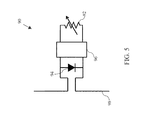
FIG. 5 shows an exemplary circuit diagram of a single rectenna; and
FIG. 6 shows a graph of current-voltage characteristics for an exemplary rectenna diode.
In the appended figures, similar components and/or features can have the same reference label. Further, various components of the same type can be distinguished by following the reference label by a second label that distinguishes among the similar components. If only the first reference label is used in the specification, the description is applicable to any one of the similar components having the same first reference label irrespective of the second reference label.
DETAILED DESCRIPTION
Ordinarily a diode rectifier in a rectenna would not require different operating voltages for different frequencies. However, quantum rectification (i.e., photon-assisted tunneling) that takes place for visible and near-infrared photons requires photon-energy-dependent (or similarly wavelength-dependent) operating voltages.
In order to take advantage of the photon-energy-dependent voltage, the present invention passively or actively splits the solar spectrum into different spectral bands, each of which is absorbed by rectennas having an operating voltage that optimizes the power conversion efficiency for that band.
As shown in FIG. 1, a radiation source (e.g., the sun, or any source of thermal radiation like a hot body) provides radiation 10 (visible/infrared) that is split by a spectral splitting device 12 into previously defined spectral frequency bands 20. The previously defined spectral frequency bands 20 are directed by the spectral splitting device 12 to rectennas 30 having customized operating voltages. The operating voltage is determined by selecting the resistance of the load for a given input power. The given input power is determined by the received spectral band. Each rectenna 30 is designed to absorb radiation over a well defined spectral band corresponding to the operating voltage for that rectenna.
In one embodiment as shown in FIG. 2, splitting of the spectrum 10 is accomplished optically, using a wavelength-selective device 40. A prism or a grating will suitably spatially split the spectrum into spectral components. The wavelength-selective device 40 sends spectral bands 21 to a group of frequency-insensitive rectennas 31 located on a substrate 34 (e.g., printed circuit board). The rectennas 31 are coplanar, with different spectral bands 21 being processed by spatially separated rectennas. In one embodiment, the antennas used in the rectennas 31 include broadband bowtie antennas.
As shown in FIG. 3, a substrate 50 includes frequency-sensitive rectennas 52 that absorb only a predefined band of wavelengths. Thus, the spectral splitting is done passively. The frequency-sensitive rectennas 52 include wavelength-selective dipole antennas 54. The spectrum is incident on the surface of the substrate 50. The frequency-sensitive rectennas 52 include a diode 51 and a load resistor 60. The diodes 51 and the load resistor 60 are configured to operate at a particular operating voltage. An example diode 51 includes a metal insulator metal (MIM) diode.
Because the dipole antennas 54 can absorb radiation over an area that is larger than their physical size, the dipole antennas 54 that are sensitive to different spectral bands are arrayed over the substrate surface 50. Different spectral portions of the total radiation (incident over the large area) are absorbed by the selective antennas occupying no more footprint than the area occupied by the incident radiation. As a result, spectral splitting is achieved by spatially separated rectennas on the same plane and does not require a grating.
As shown in FIG. 4, a rectenna system 70 includes stacks of semi-permeable substrates 72 that include one or more frequency-sensitive rectenna 74. Each level of the stack of rectennas absorbs different frequency bands. Thus, non-absorbed frequency bands penetrate to the next substrate layer 72. The material chosen depends on the incident spectrum (visible, NIR, long wavelength IR). Examples include quartz, fused silica, transparent polymers/plastics, calcium fluoride and potassium bromide IR transparent substrates.
In another embodiment, a single broadband antenna absorbs the entire spectrum of interest, or a substantial fraction of it. The electric current coming from the antenna is split into frequency bands, and each frequency band of current is directed to a separate diode whose operating voltage is tuned for that band. One way to accomplish the splitting is with the use of passive inductor-capacitor (LC) filters, as is conventionally used to filter ac signals.
FIG. 5 shows an exemplary rectenna circuit 90. The rectenna circuit 90 includes an adjustable load resistor 92, an antenna (frequency sensitive or insensitive) 98, a diode 94 and a DC output filter 96. The DC output filter 96 blocks AC power dissipation in the load resistor 92. The adjustable load resistor 92 is adjusted to provide a desired voltage across the diode 94.
FIG. 6 shows current-voltage [I(V)] characteristics for a rectenna diode (such as the diode 94). The solid curve 100 is the I(V) for an exemplary rectenna in the dark (i.e., not exposed to the spectral source), and the dashed curve 102 shows the I(V) under illumination from a specific spectral band. The voltage at which the dashed curve 102 crosses the Voltage axis is equal to the photon energy divided by the electron charge. The location where the curve 102 crosses the v-axis indicates the maximum voltage that the rectenna can extract from the incident spectrum. Beyond this voltage, the current is negative and the rectenna cannot generate any energy. For an ideal rectenna diode illuminated by a monochromatic source, the rectenna efficiency approaches 100% when the bias voltage is equal to the photon energy divided by the electron charge. Therefore, for a high-photon-energy slice (band) of the spectrum the dashed line 102 extends farther to the left on the Voltage axis than for a low-photon-energy slice. A load-line 106 intersects the rectenna illuminated I(V) (the dashed curve 102) at the operating voltage Vo. Rectenna output power is the area under the dashed curve 102 at the load-line 106 intersection. The slope of the load-line 106 and hence the operating voltage can be chosen for high rectenna efficiency by tuning the load impedance. The illuminated I(V) curve (dashed curve in FIG. 6) is a function of the power and the energies of the different photons in the incident spectral band.
All the different spectral bands (i.e., frequencies) can be absorbed using rectennas composed of the same materials. The spectral sensitivity is determined by the operating voltage, and can also be affected by the antenna design and size. This provides a great reduction in the cost of making a wide spectral band rectenna system. This is particularly advantageous over spectrum splitting in conventional solar cells, where different materials are required for each spectral region.
For optimum efficiency, the diode I(V) characteristic has to be such that the diode impedance presented to a slice of the spectrum is matched to the antenna impedance. This results in maximum power transfer from the antenna to the diode. Also, the diode must have a fast response time so that its RC time constant is less than the inverse of (2 times π times the maximum frequency in the incident band).
The present invention applies to solar radiation and to any broad optical or infrared spectrum (e.g., near, mid, and long-wave IR spectrum). For example, power conversion from a hot object or source that produces blackbody radiation in the infrared would also benefit from the spectrum-splitting approach that is taught in detail herein.
Other examples and implementations are within the scope and spirit of the disclosure and appended claims. For example, features implementing functions can also be physically located at various positions, including being distributed such that portions of functions are implemented at different physical locations. Also, as used herein, including in the claims, “or” as used in a list of items prefaced by “at least one of” indicates a disjunctive list such that, for example, a list of “at least one of A, B, or C” means A or B or C or AB or AC or BC or ABC (i.e., A and B and C). Further, the term “exemplary” does not mean that the described example is preferred or better than other examples.
Various changes, substitutions, and alterations to the techniques described herein can be made without departing from the technology of the teachings as defined by the appended claims. Moreover, the scope of the disclosure and claims is not limited to the particular aspects of the process, machine, manufacture, composition of matter, means, methods, and actions described above. Processes, machines, manufacture, compositions of matter, means, methods, or actions, presently existing or later to be developed, that perform substantially the same function or achieve substantially the same result as the corresponding aspects described herein can be utilized. Accordingly, the appended claims include within their scope such processes, machines, manufacture, compositions of matter, means, methods, or actions.

Claims (17)

What is claimed is:
1. A rectenna system comprising:
a plurality of antennas configured to receive at least one of a visible or infrared spectrum; and
a plurality of rectifying circuits coupled to the antennas, each rectifying circuit configured to generate a current based on a portion of the spectrum received by the antennas,
wherein each rectifying circuit has an operating voltage based on a different frequency band of the spectrum received by the antennas.
2. The rectenna system of claim 1, wherein at least one of the rectifying circuits comprises a diode and a load resistor, wherein the diode and the load resistor are coupled in parallel to the at least one antenna.
3. The rectenna system of claim 1, further comprising a spectral splitting device configured to split the received spectrum into at least two spectrum bands.
4. The rectenna system of claim 1, wherein the plurality of rectifying circuits and the coupled antennas defines a plurality of rectennas, wherein the plurality of rectennas are located on a single substrate configured to receive the at least two spectrum bands.
5. The rectenna system of claim 1, wherein the plurality of rectifying circuits and the coupled antennas defines a plurality of rectennas, wherein at least one of the plurality of rectennas is located on a first substrate configured to allow at least a portion of the spectrum to pass through and wherein at least another of the plurality of rectennas is located on a second substrate.
6. The rectenna system of claim 1, wherein the at least one antenna comprises at least one dipole antenna.
7. The rectenna system of claim 1, wherein the at least one antenna comprises at least one bowtie antenna.
8. The rectenna system of claim 2, wherein the load resistor is a variable load resistor.
9. The rectenna system of claim 5, wherein the first substrate and second substrate are located at different distances along an incident path of the received spectrum.
10. A method comprising:
receiving, with a plurality of antennas, at least one of a visible or infrared spectrum; and
generating, with each of a plurality of rectifying circuits coupled to a respective at least one of the antennas, a current based on a portion of the spectrum received by the respective at least one of the antennas,
wherein each rectifying circuit has an operating voltage based on a different frequency band of the spectrum received by the respective at least one of the antennas.
11. The method of claim 10, further comprising optically splitting the received spectrum before being received by the antennas.
12. The method of claim 10, wherein receiving comprising receiving a portion of the received spectrum at the antennas.
13. A rectenna system comprising:
a plurality of rectennas, each rectenna comprising:
an antenna configured to receive at least a portion of a visible or infrared spectrum;
a diode; and
a load resistor,
wherein the diode and the load resistor are coupled in parallel to the antenna,
wherein each of the rectennas has an operating voltage based on a different frequency band of the spectrum.
14. The rectenna system of claim 13, wherein a value for the load resistor of a first one of the rectennas is based on a first frequency band of the received spectrum,
wherein a value for the load resistor of a second one of the rectennas is based on a second frequency band of the received spectrum.
15. The rectenna system of claim 14, wherein at least one of the rectennas are mounted on each of a plurality of substrates, wherein the substrates are placed in stacked formation relative to an incident angle of the received spectrum portion.
16. The rectenna system of claim 14, wherein each of the rectennas are mounted on a substrate.
17. The rectenna system of claim 16, wherein the antennas are configured to receive different portions of the spectrum.
US14/063,728 2013-01-30 2013-10-25 Spectrum splitting using optical rectennas Expired - Fee Related US9255840B2 (en)

Priority Applications (1)

Application Number Priority Date Filing Date Title
US14/063,728 US9255840B2 (en) 2013-01-30 2013-10-25 Spectrum splitting using optical rectennas

Applications Claiming Priority (2)

Application Number Priority Date Filing Date Title
US201361758578P 2013-01-30 2013-01-30
US14/063,728 US9255840B2 (en) 2013-01-30 2013-10-25 Spectrum splitting using optical rectennas

Publications (2)

Publication Number Publication Date
US20140209788A1 US20140209788A1 (en) 2014-07-31
US9255840B2 true US9255840B2 (en) 2016-02-09

Family

ID=51221893

Family Applications (1)

Application Number Title Priority Date Filing Date
US14/063,728 Expired - Fee Related US9255840B2 (en) 2013-01-30 2013-10-25 Spectrum splitting using optical rectennas

Country Status (2)

Country Link
US (1) US9255840B2 (en)
CN (1) CN103966223A (en)

Families Citing this family (1)

* Cited by examiner, † Cited by third party
Publication number Priority date Publication date Assignee Title
WO2015005904A1 (en) * 2013-07-09 2015-01-15 Halliburton Energy Services, Inc. Integrated computational elements with frequency selective surface

Citations (2)

* Cited by examiner, † Cited by third party
Publication number Priority date Publication date Assignee Title
US20070170505A1 (en) * 2005-12-27 2007-07-26 Hajime Tokunaga Semiconductor device and manufacturing method thereof
US20080268796A1 (en) * 2007-04-27 2008-10-30 Ntt Docomo, Inc Radio communication device and power supplying method for radio communication device

Family Cites Families (3)

* Cited by examiner, † Cited by third party
Publication number Priority date Publication date Assignee Title
AU2002310031A1 (en) * 2001-05-23 2002-12-03 University Of Florida Method and apparatus for detecting illicit substances
CN104745585B (en) * 2013-12-27 2020-02-04 上海市刑事科学技术研究院 Methamphetamine aptamer, detection kit and application thereof
CN105624164B (en) * 2014-10-31 2020-12-01 上海市刑事科学技术研究院 Ketamine aptamer, detection kit and application thereof

Patent Citations (2)

* Cited by examiner, † Cited by third party
Publication number Priority date Publication date Assignee Title
US20070170505A1 (en) * 2005-12-27 2007-07-26 Hajime Tokunaga Semiconductor device and manufacturing method thereof
US20080268796A1 (en) * 2007-04-27 2008-10-30 Ntt Docomo, Inc Radio communication device and power supplying method for radio communication device

Non-Patent Citations (18)

* Cited by examiner, † Cited by third party
Title
Agarwal, et al, "Coherence Properties of Sunlight", Optics Letters, Mar. 1, 2004, vol. 29, No. 5, pp. 459-461.
Alda , et al.,"Optical antennas for nano-photonic applications", Nanotechnology, Mar. 4, 2005, vol. 16, pp. S230-S234.
Berland, B. "Photovoltaic Technologies Beyond the Horizon: Optical Rectenna Solar Cell" Subcontractor Report, Feb. 2003, NREL/SR-520-33263.
Corkish, et al., "Solar Collection by Antennas", Solar Energy, Jan. 29, 2003, vol. 73, No. 6, pp. 395-401.
Dayhem, et al.,"Quantum Interaction of Microwave Radiation with Tunneling Between Superconductors", Physical Review Letters, Mar. 15, 1962, vol. 8, No. 6, pp. 246-249.
Grover et al., "Engineering the current-voltage characteristics of metal-insulator-metal diodes using double-insulator tunnel barriers", Solid-State Electronics, 2012, vol. 67, pp. 94-99.
Grover, et al., "Applicability of Metal/Insulator/Metal (MIM) Diodes to Solar Rectennas", Jul. 2011, vol. 1, No. 1, pp. 78-83.
Grover, Sachit "Diodes for Optical Rectennas", Thesis submitted to the Faculty of the Graduate School of the University of Colorado, 2011.
Hamilton, et al., "rf-Induced Effects in Superconducting Tunnel Junctions", Dec. 1, 1970, vol. 2, No. 1, pp. 4494-4505.
Markvart, Tom, "Themodynamics of losses in photovoltaic conversion", 2007, vol. 91, Issue No. 064102.
Mashaal, et al., "Fundamental bounds for antenna harvesting of sunlight", Optics Letters, Mar. 15, 2011, vol. 36, No. 6, pp. 900-902.
Shockley, et al., "Detailed Balance Limit of Efficiency of pn Junction Solar Cells", Mar. 1961, Journal of Applied Physics, Mar. 1961, vol. 32, No. 3, pp. 510-519.
Tien et al, "Multiphoton Process Observed in the Interaction of Microwave Fields with the Tunneling between Superconductor Films", Physical Review, Jan. 15, 1963, vol. 129, No. 2, pp. 647-651.
Tucker, John R., "Quantam detection at millimeter wavelengths", Reviews of Modern Physics, Oct. 1985, vol. 57, No. 4, pp. 1055-1114.
Tucker, John R., "Quantum Limited Detection in Tunnel Junction Mixers",IEEE Journal of Quantum Electronics, Nov. 11, 1979, vol. QE-15, No. 11, pp. 1234-1258.
Vandenbosch, et al., "Upper bounds for the solar energy harvesting efficiency of nano-antennas", Nano Energy, Mar. 13, 2012, vol. 1, pp. 494-502.
Werthamer, N.R., "Nonlinear Self-Coupling of Josephson Radiation in Superconducting Tunnel Junctions", Physical Review, Jul. 8, 1966, vol. 147, No. 1, pp. 255-263.
Withington, et al., "Multitone quantum simulations of saturating tunnel junction mixers", Journal of Applied Physics, Jun. 15, 2003, vol. 93, No. 2, pp. 9812-9819.

Also Published As

Publication number Publication date
US20140209788A1 (en) 2014-07-31
CN103966223A (en) 2014-08-06

Similar Documents

Publication Publication Date Title
Mavaddat et al. Millimeter-Wave Energy Harvesting Using $4\times4 $ Microstrip Patch Antenna Array
Gu et al. Far-field wireless power harvesting: Nonlinear modeling, rectenna design, and emerging applications
US20100284086A1 (en) Structures, systems and methods for harvesting energy from electromagnetic radiation
US20210044004A1 (en) Electromagnetic energy harvesting devices and methods
KR20100129698A (en) Photovoltaic power generation system and photovoltaic power generation device
Liang et al. A compact dual-band four-port ambient RF energy harvester with high-sensitivity, high-efficiency, and wide power range
Abadal et al. Chapter Electromagnetic Radiation Energy Harvesting–The Rectenna Based Approach
Kapilevich et al. W-band rectenna coupled with low-barrier mott diode
JP6222667B2 (en) Storage type solar power generation device and storage type solar power generation system
Xu et al. Transmissive concentrator multijunction solar cells with over 47% in-band power conversion efficiency
Hillger et al. An antenna-coupled 0.49 THz SiGe HBT source for active illumination in terahertz imaging applications
US9255840B2 (en) Spectrum splitting using optical rectennas
Midrio et al. Nano-antenna array for high efficiency sunlight harvesting
Chuc et al. Investigation of rectifier circuit configurations for microwave power transmission system operating at S Band
US11444218B2 (en) Device for operating with THz and/or IR and/or MW radiation
Ito et al. Widely frequency tunable terahertz-wave emitter integrating uni-traveling-carrier photodiode and extended bowtie antenna
Hamani et al. Design of rectenna series‐association circuits for radio frequency energy harvesting in CMOS FD‐SOI 28 nm
Gangwar et al. Design and analysis of a pentagonal rectenna
Moon et al. Photo-conductive detection of continuous THz waves via manipulated ultrafast process in nanostructures
Aldrigo et al. Graphene-based nano-rectenna in the far infrared frequency band
EP3379645B1 (en) Solar antenna comprising graphene, solar unit comprising multiple solar antennas and method for operating a solar unit
Nakashima et al. Performance of 5.8-GHz multi-polarization rectenna for linearly/circularly polarized wave reception
Slepyan et al. Quantum light rectification in nano-rectennas
Aldrigo et al. Numerical analysis of an innovative energy-harvesting system in the infrared region
Seniutinas et al. THz photomixer with a 40nm-wide nanoelectrode gap on low-temperature grown GaAs

Legal Events

Date Code Title Description
AS Assignment

Owner name: THE REGENTS OF THE UNIVERSITY OF COLORADO, A BODY

Free format text: ASSIGNMENT OF ASSIGNORS INTEREST;ASSIGNORS:MODEL, GARRETT;JOSHI, SAUMIL;REEL/FRAME:031481/0571

Effective date: 20131024

AS Assignment

Owner name: THE REGENTS OF THE UNIVERSITY OF COLORADO, A BODY

Free format text: CORRECTIVE ASSIGNMENT TO CORRECT THE NAME OF THE FIRST NAMED INVENTOR TO GARRET MODDEL PREVIOUSLY RECORDED ON REEL 031481 FRAME 0571. ASSIGNOR(S) HEREBY CONFIRMS THE ASSIGNMENT OF ASSIGNORS NTEREST;ASSIGNORS:MODDEL, GARRET;JOSHI, SAUMIL;REEL/FRAME:031508/0421

Effective date: 20131024

STCF Information on status: patent grant

Free format text: PATENTED CASE

FEPP Fee payment procedure

Free format text: MAINTENANCE FEE REMINDER MAILED (ORIGINAL EVENT CODE: REM.); ENTITY STATUS OF PATENT OWNER: SMALL ENTITY

LAPS Lapse for failure to pay maintenance fees

Free format text: PATENT EXPIRED FOR FAILURE TO PAY MAINTENANCE FEES (ORIGINAL EVENT CODE: EXP.); ENTITY STATUS OF PATENT OWNER: SMALL ENTITY

STCH Information on status: patent discontinuation

Free format text: PATENT EXPIRED DUE TO NONPAYMENT OF MAINTENANCE FEES UNDER 37 CFR 1.362

FP Expired due to failure to pay maintenance fee

Effective date: 20200209