US9159888B2 - Wafer level phosphor coating method and devices fabricated utilizing method - Google Patents
Wafer level phosphor coating method and devices fabricated utilizing method Download PDFInfo
- Publication number
- US9159888B2 US9159888B2 US11/899,790 US89979007A US9159888B2 US 9159888 B2 US9159888 B2 US 9159888B2 US 89979007 A US89979007 A US 89979007A US 9159888 B2 US9159888 B2 US 9159888B2
- Authority
- US
- United States
- Prior art keywords
- coating
- led
- led chip
- leds
- wafer
- Prior art date
- Legal status (The legal status is an assumption and is not a legal conclusion. Google has not performed a legal analysis and makes no representation as to the accuracy of the status listed.)
- Active
Links
Images


Classifications
-
- H—ELECTRICITY
- H01—ELECTRIC ELEMENTS
- H01L—SEMICONDUCTOR DEVICES NOT COVERED BY CLASS H10
- H01L33/00—Semiconductor devices with at least one potential-jump barrier or surface barrier specially adapted for light emission; Processes or apparatus specially adapted for the manufacture or treatment thereof or of parts thereof; Details thereof
- H01L33/48—Semiconductor devices with at least one potential-jump barrier or surface barrier specially adapted for light emission; Processes or apparatus specially adapted for the manufacture or treatment thereof or of parts thereof; Details thereof characterised by the semiconductor body packages
- H01L33/50—Wavelength conversion elements
- H01L33/508—Wavelength conversion elements having a non-uniform spatial arrangement or non-uniform concentration, e.g. patterned wavelength conversion layer, wavelength conversion layer with a concentration gradient of the wavelength conversion material
-
- H—ELECTRICITY
- H01—ELECTRIC ELEMENTS
- H01L—SEMICONDUCTOR DEVICES NOT COVERED BY CLASS H10
- H01L33/00—Semiconductor devices with at least one potential-jump barrier or surface barrier specially adapted for light emission; Processes or apparatus specially adapted for the manufacture or treatment thereof or of parts thereof; Details thereof
- H01L33/48—Semiconductor devices with at least one potential-jump barrier or surface barrier specially adapted for light emission; Processes or apparatus specially adapted for the manufacture or treatment thereof or of parts thereof; Details thereof characterised by the semiconductor body packages
- H01L33/62—Arrangements for conducting electric current to or from the semiconductor body, e.g. lead-frames, wire-bonds or solder balls
-
- H—ELECTRICITY
- H01—ELECTRIC ELEMENTS
- H01L—SEMICONDUCTOR DEVICES NOT COVERED BY CLASS H10
- H01L2924/00—Indexing scheme for arrangements or methods for connecting or disconnecting semiconductor or solid-state bodies as covered by H01L24/00
-
- H—ELECTRICITY
- H01—ELECTRIC ELEMENTS
- H01L—SEMICONDUCTOR DEVICES NOT COVERED BY CLASS H10
- H01L2924/00—Indexing scheme for arrangements or methods for connecting or disconnecting semiconductor or solid-state bodies as covered by H01L24/00
- H01L2924/0001—Technical content checked by a classifier
- H01L2924/0002—Not covered by any one of groups H01L24/00, H01L24/00 and H01L2224/00
-
- H—ELECTRICITY
- H01—ELECTRIC ELEMENTS
- H01L—SEMICONDUCTOR DEVICES NOT COVERED BY CLASS H10
- H01L2933/00—Details relating to devices covered by the group H01L33/00 but not provided for in its subgroups
- H01L2933/0091—Scattering means in or on the semiconductor body or semiconductor body package
-
- H—ELECTRICITY
- H01—ELECTRIC ELEMENTS
- H01L—SEMICONDUCTOR DEVICES NOT COVERED BY CLASS H10
- H01L33/00—Semiconductor devices with at least one potential-jump barrier or surface barrier specially adapted for light emission; Processes or apparatus specially adapted for the manufacture or treatment thereof or of parts thereof; Details thereof
- H01L33/005—Processes
- H01L33/0095—Post-treatment of devices, e.g. annealing, recrystallisation or short-circuit elimination
-
- H—ELECTRICITY
- H01—ELECTRIC ELEMENTS
- H01L—SEMICONDUCTOR DEVICES NOT COVERED BY CLASS H10
- H01L33/00—Semiconductor devices with at least one potential-jump barrier or surface barrier specially adapted for light emission; Processes or apparatus specially adapted for the manufacture or treatment thereof or of parts thereof; Details thereof
- H01L33/36—Semiconductor devices with at least one potential-jump barrier or surface barrier specially adapted for light emission; Processes or apparatus specially adapted for the manufacture or treatment thereof or of parts thereof; Details thereof characterised by the electrodes
- H01L33/38—Semiconductor devices with at least one potential-jump barrier or surface barrier specially adapted for light emission; Processes or apparatus specially adapted for the manufacture or treatment thereof or of parts thereof; Details thereof characterised by the electrodes with a particular shape
- H01L33/387—Semiconductor devices with at least one potential-jump barrier or surface barrier specially adapted for light emission; Processes or apparatus specially adapted for the manufacture or treatment thereof or of parts thereof; Details thereof characterised by the electrodes with a particular shape with a plurality of electrode regions in direct contact with the semiconductor body and being electrically interconnected by another electrode layer
-
- H—ELECTRICITY
- H01—ELECTRIC ELEMENTS
- H01L—SEMICONDUCTOR DEVICES NOT COVERED BY CLASS H10
- H01L33/00—Semiconductor devices with at least one potential-jump barrier or surface barrier specially adapted for light emission; Processes or apparatus specially adapted for the manufacture or treatment thereof or of parts thereof; Details thereof
- H01L33/44—Semiconductor devices with at least one potential-jump barrier or surface barrier specially adapted for light emission; Processes or apparatus specially adapted for the manufacture or treatment thereof or of parts thereof; Details thereof characterised by the coatings, e.g. passivation layer or anti-reflective coating
-
- H—ELECTRICITY
- H01—ELECTRIC ELEMENTS
- H01L—SEMICONDUCTOR DEVICES NOT COVERED BY CLASS H10
- H01L33/00—Semiconductor devices with at least one potential-jump barrier or surface barrier specially adapted for light emission; Processes or apparatus specially adapted for the manufacture or treatment thereof or of parts thereof; Details thereof
- H01L33/48—Semiconductor devices with at least one potential-jump barrier or surface barrier specially adapted for light emission; Processes or apparatus specially adapted for the manufacture or treatment thereof or of parts thereof; Details thereof characterised by the semiconductor body packages
- H01L33/50—Wavelength conversion elements
- H01L33/505—Wavelength conversion elements characterised by the shape, e.g. plate or foil
-
- H—ELECTRICITY
- H01—ELECTRIC ELEMENTS
- H01L—SEMICONDUCTOR DEVICES NOT COVERED BY CLASS H10
- H01L33/00—Semiconductor devices with at least one potential-jump barrier or surface barrier specially adapted for light emission; Processes or apparatus specially adapted for the manufacture or treatment thereof or of parts thereof; Details thereof
- H01L33/48—Semiconductor devices with at least one potential-jump barrier or surface barrier specially adapted for light emission; Processes or apparatus specially adapted for the manufacture or treatment thereof or of parts thereof; Details thereof characterised by the semiconductor body packages
- H01L33/52—Encapsulations
- H01L33/54—Encapsulations having a particular shape
Definitions
- This invention relates to methods for fabricating semiconductor devices and in particular methods for wafer level coating of light emitting diodes.
- LED Light emitting diodes
- LED Light emitting diodes
- LEDs are solid state devices that convert electric energy to light, and generally comprise one or more active layers of semiconductor material sandwiched between oppositely doped layers. When a bias is applied across the doped layers, holes and electrons are injected into the active layer where they recombine to generate light. Light is emitted from the active layer and from all surfaces of the LED.
- LEDs cannot generate white light from their active layers.
- Light from a blue emitting LED has been converted to white light by surrounding the LED with a yellow phosphor, polymer or dye, with a typical phosphor being cerium-doped yttrium aluminum garnet (Ce:YAG).
- Ce:YAG cerium-doped yttrium aluminum garnet
- the surrounding phosphor material “downconverts” the wavelength of some of the LED's blue light, changing its color to yellow.
- the LED emits both blue and yellow light, which combine to provide a white light.
- light from a violet or ultraviolet emitting LED has been converted to white light by surrounding the LED with multicolor phosphors or dyes.
- One conventional method for coating an LED with a phosphor layer utilizes a syringe or nozzle for injecting a phosphor mixed with epoxy resin or silicone polymers over the LED.
- a syringe or nozzle for injecting a phosphor mixed with epoxy resin or silicone polymers over the LED.
- light emitting from the LED at different angles can pass through different amounts of conversion material, which can result in an LED with non-uniform color temperature as a function of viewing angle.
- the geometry and thickness is hard to control, it can also be difficult to consistently reproduce LEDs with the same or similar emission characteristics.
- Another conventional method for coating an LED is by stencil printing, which is described in European Patent Application EP 1198016 A2 to Lowery.
- Multiple light emitting semiconductor devices are arranged on a substrate with a desired distance between adjacent LEDs.
- the stencil is provided having openings that align with the LEDs, with the holes being slightly larger than the LEDs and the stencil being thicker than the LEDs.
- a stencil is positioned on the substrate with each of the LEDs located within a respective opening in the stencil.
- a composition is then deposited in the stencil openings, covering the LEDs, with a typical composition being a phosphor in a silicone polymer that can be cured by heat or light. After the holes are filled, the stencil is removed from the substrate and the stenciling composition is cured to a solid state.
- the stenciling composition may not fully fill the stencil opening such that the resulting layer is not uniform.
- the phosphor containing composition can also stick to the stencil opening which reduces the amount of composition remaining on the LED.
- the stencil openings may also be misaligned to the LED.
- the key challenge is accessing the wire bond pad on the device after the coating process.
- Accessing the wire bond by standard wafer fabrication techniques is difficult with typical silicone binding material, as well as other binder materials such as epoxies or glass.
- Silicones are not compatible with commonly used wafer fabrication materials such as acetone, as well as some developers, and resist strippers. This can limit the options and choices for the particular silicones and process steps. Silicones are also cured at high temperature (greater than 150° C.), which is beyond the glass transition temperature of commonly used photoresists. Cured silicone films with phosphor are also difficult to etch and have a very slow etch rate in chlorine and CF 4 plasma, and wet etching of cured silicones is typically inefficient.
- the present invention discloses new methods for fabricating semiconductor devices such as LED chips at the wafer level, and discloses LED chips and LED chip wafers fabricated using the methods.
- One method for fabricating light emitting diode (LED) chips according to the present invention comprises providing a plurality of LEDs typically on a substrate. Pedestals are formed on the LEDs with each of the pedestals in electrical contact with one of the LEDs. A coating is formed over said LEDs, with the coating burying at least some of the pedestals. The coating is then planarized leaving some of said coating material on said LEDs while exposing at least some of the buried pedestals, making them available for contacting.
- the present invention discloses similar methods used for fabricating LED chips comprising LEDs flip chip mounted on a carrier substrate. Similar methods according to the present invention can also be used for fabricating other semiconductor devices.
- One embodiment of a light emitting diode (LED) chip wafer fabricated using methods according to the present invention comprises a plurality of LEDs on a substrate wafer and a plurality of pedestals, each of which is in electrical contact with one of the LEDs.
- a coating at least partially covers the LEDs with at least some of the pedestals extending through and to the surface of the coating. The pedestals are exposed at the surface of the coating.
- One embodiment of a light emitting diode (LED) chip manufactured using methods according to the present invention comprises an LED on a substrate and a pedestal in electrical contact with the LED. A coating at least partially covering the LED, with the pedestal extending through and to the surface of the coating and exposed at the surface of the coating.
- LED light emitting diode
- the coating can include phosphor particles that downconvert at least some of the light emitted from the active region of the LED chip to produce white light, thereby producing a white LED chip.
- FIGS. 1 a through 1 e are sectional views of one embodiment of an LED chip wafer at fabrication steps in one method according to the present invention
- FIGS. 2 a through 2 g are sectional views of another embodiment of an LED chip wafer at fabrication steps in another method according to the present invention.
- FIG. 3 is a sectional view of another embodiment of an LED chip wafer according to the present invention having microwire pedestals;
- FIG. 4 is a sectional view of another embodiment of an LED chip wafer according to the present invention having a reflective layer
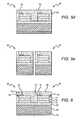
- FIGS. 5 a through 5 e are sectional views of one embodiment of a flip-wafer bonded LED chip wafer at fabrication steps in another method according to the present invention.
- FIG. 6 is a sectional view of another embodiment of an LED chip wafer according to the present invention having a reflective layer
- FIG. 7 is a flow diagram for one embodiment of a method according to the present invention for fabricating LED chips
- FIGS. 8 a through 8 d are sectional views of another embodiment of an LED chip wafer at fabrication steps in a method according to the present invention utilizing a prefabricated coating;
- FIGS. 9 a through 9 c are sectional views of another embodiment of an LED chip wafer at fabrication steps in a method according to the present invention having recesses in the coating;
- FIG. 10 is a sectional view of another embodiment of an LED chip wafer according to the present invention.
- FIG. 11 is also a sectional view of another embodiment of an LED chip wafer according to the present invention.
- FIG. 12 is a sectional view of one embodiment of an LED array according to the present invention.
- FIG. 13 is a sectional view of another embodiment of an LED array according to the present invention.
- FIG. 14 is a sectional view of an embodiment of an LED chip wafer according to the present invention having a transparent substrate
- FIG. 15 is a sectional view of another embodiment of an LED chip wafer according to the present invention having a transparent substrate;
- FIG. 16 is a sectional view of another embodiment of an flip-chip LED chip wafer according to the present invention.
- FIG. 17 is a sectional view of another embodiment of an LED chip having a phosphor loading carrier substrate
- FIGS. 18 a through 18 d are sectional views of another embodiment of an LED chip wafer at fabrication steps in a method according to the present invention utilizing a trenched substrate;
- FIG. 19 is a sectional view of another embodiment of an LED chip according to the present invention having a textured surface
- FIG. 20 is a top view of another embodiment of an LED chip according to the present invention having a current spreading structure
- FIG. 21 is a sectional view of another embodiment of an LED chip according to the present invention having a textured surface
- FIG. 22 is a sectional view of another embodiment of an LED chip according to the present invention having a textured surface
- FIG. 23 is a sectional view of another embodiment of an LED chip according to the present invention.
- FIG. 24 is a sectional view of another embodiment of an LED chip according to the present invention.
- FIG. 25 is a sectional view of another embodiment of an LED chip according to the present invention.
- FIG. 26 is a sectional view of another embodiment of an LED chip according to the present invention.
- FIG. 27 is a sectional view of another embodiment of an LED chip according to the present invention having a dome shaped coating
- FIG. 28 is a sectional view of another embodiment of an LED chip according to the present invention having a concave shaped coating
- FIG. 29 is a sectional view of another embodiment of an LED chip according to the present invention having a coating with a textured surface;
- FIG. 30 is a sectional view of another embodiment of an LED chip according to the present invention having portions with different concentrations of phosphors;
- FIG. 31 is a sectional view of another embodiment of an LED chip according to the present invention having portions with different concentrations of phosphors;
- FIG. 32 is a sectional view of an LED package according to the present invention.
- FIG. 33 is a top view of the LED package in FIG. 32 ;
- FIG. 34 is a table showing performance characteristics for an LED package according to the present invention.
- FIG. 35 is graph showing performance characteristics for different LED packages according to the present invention.
- the present invention provides fabrication methods that are particularly applicable to wafer level coating of semiconductor devices such as LEDs.
- the present invention also provides semiconductor devices, such as LEDs fabricated using these methods.
- the present invention allows coating of LEDs at the wafer level with a down-converter layer (e.g. phosphor loaded silicone) while still allowing access to one or more of the contacts for wire bonding.
- electrically conducting pedestals/posts are formed on one or both of the LED contacts (bond pads) while the LEDs are at the wafer level. These pedestals can be fabricated using known techniques such as electroplating, electroless plating, stud bumping, or vacuum deposition.
- the wafer can then be blanket coated with a down-converter coating layer, burying the LEDs, contacts and pedestals.
- a down-converter coating layer burying the LEDs, contacts and pedestals.
- Each of the pedestals act as a vertical extension of its contact, and although the blanket coating with the down-converter coating temporarily covers the pedestals, the coating can be planarized and thinned to expose the top surface or top portion of the pedestals.
- the pedestals should be tall enough (10-100 ⁇ m) to project through the desired final coating thickness. After planarizing the pedestals are exposed for external connection such as by wire bonding. This process occurs at the wafer level and at a subsequent fabrication step, the individual LEDs chips can be separated/singulated from the wafer using known processes.
- the present invention eliminates complex wafer fabrication processes to access wire bond pads after blanket coating. Instead a simple and cost effective approach is utilized. It allows for wafer level coating of semiconductor devices without the need for alignment.
- a wide variety of coating technologies can be used such as spin-coating of phosphor loaded silicone mixture, or electrophoretic deposition of phosphor followed by blanket coating of silicone or other binding material.
- Mechanical planarization allows thickness uniformity over the wafer and thickness uniformity of the coat can be achieved over a wide thickness range (e.g. 1 to 100 ⁇ m).
- White LED chip color point may be fine tuned by controlling the final coat thickness, including using an iterative approach (e.g. grind, test, grind, etc.) which will result in tightly binned white LEDs. This approach is also scalable to large wafer sizes.
- the present invention is described herein with reference to certain embodiments but it is understood that the invention can be embodied in many different forms and should not be construed as limited to the embodiments set forth herein.
- the present invention is described below in regards to coating LEDs with a down-converter coating that typically comprises a phosphor loaded binder (“phosphor/binder coating”), but it is understood that the present invention can be used to coat LEDs with other materials for down-conversion, protection, light extraction or scattering.
- the phosphor binder can have scattering or light extraction particles or materials, and that the coating can be electrically active.
- the methods according to the present invention can also be used for coating other semiconductor devices with different materials.
- a coating can include no phosphors, one or more phosphors, scattering particles and/or other materials.
- a coating may also comprise a material such as an organic dye that provides down-conversion. With multiple coatings and/or layers, each one can include different phosphors, different scattering particles, different optical properties, such as transparency, index of refraction, and/or different physical properties, as compared to other layers and/or coatings.
- first, second, etc. may be used herein to describe various elements, components, regions, layers and/or sections, these elements, components, regions, layers and/or sections should not be limited by these terms. These terms are only used to distinguish one element, component, region, layer or section from another region, layer or section. Thus, a first element, component, region, layer or section discussed below could be termed a second element, component, region, layer or section without departing from the teachings of the present invention.
- Embodiments of the invention are described herein with reference to cross-sectional view illustrations that are schematic illustrations of idealized embodiments of the invention. As such, variations from the shapes of the illustrations as a result, for example, of manufacturing techniques and/or tolerances are expected. Embodiments of the invention should not be construed as limited to the particular shapes of the regions illustrated herein but are to include deviations in shapes that result, for example, from manufacturing. A region illustrated or described as square or rectangular will typically have rounded or curved features due to normal manufacturing tolerances. Thus, the regions illustrated in the figures are schematic in nature and their shapes are not intended to illustrate the precise shape of a region of a device and are not intended to limit the scope of the invention.
- FIGS. 1 a through 1 e show one embodiment of wafer level LED chips 10 manufactured using a method according to the present invention.
- the LEDs chips 10 are shown at a wafer level of their fabrication process. That is, the LEDs chips 10 have not been through all the steps necessary before being separated/singulated from wafer into individual LED chips. Phantom lines are included to show separation or dicing line between the LED chips 10 and following additional fabrication steps, and as shown in FIG. 1 e the LEDs chips can be separated into individual devices.
- FIGS. 1 a through 1 e also show only two devices at the wafer level, but it is understood that many more LED chips can be formed from a single wafer. For example, when fabricating LED chips having a 1 millimeter (mm) square size, up to 4500 LED chips can be fabricated on a 3 inch wafer.
- mm millimeter
- Each of the LED chips 10 comprises a semiconductor LED 12 that can have many different semiconductor layers arranged in different ways.
- the fabrication and operation of LEDs is generally known in the art and only briefly discussed herein.
- the layers of the LED 10 can be fabricated using known processes with a suitable process being fabrication using metal organic chemical vapor deposition (MOCVD).
- the layers of the LEDs 12 generally comprise an active layer/region 14 sandwiched between first and second oppositely doped epitaxial layers 16 , 18 , all of which are formed successively on a substrate 20 .
- the LEDs 12 are shown as separate devices on the substrate 20 . This separation can be achieved by having portions of the active region 14 and doped layers 16 , 18 etched down to the substrate 20 to form the open areas between the LEDs 12 .
- the active layer 14 and doped layers 16 , 18 can remain continuous layers on the substrate 20 and can be separated into individual devices when the LED chips are singulated.
- the active region 14 can comprise single quantum well (SQW), multiple quantum well (MQW), double heterostructure or super lattice structures.
- the first epitaxial layer 16 is an n-type doped layer and the second epitaxial layer 18 is a p-type doped layer, although in other embodiments the first layer 16 can be p-type doped and the second layer 18 n-type doped.
- the first and second epitaxial layers 16 , 18 are hereinafter referred to as n-type and p-type layers, respectively.
- the region 14 and layers 16 , 18 of the LEDs 12 may be fabricated from different material systems, with preferred material systems being Group-III nitride based material systems.
- Group-III nitrides refer to those semiconductor compounds formed between nitrogen and the elements in the Group III of the periodic table, usually aluminum (Al), gallium (Ga), and indium (In).
- AlGaN aluminum gallium nitride
- AlInGaN aluminum indium gallium nitride
- the n- and p-type layers 16 , 18 are gallium nitride (GaN) and the active region 14 is InGaN.
- n- and p-type layers 16 , 18 may be AlGaN, aluminum gallium arsenide (AlGaAs) or aluminum gallium indium arsenide phosphide (AlGaInAsP).
- the substrate 20 can be made of many materials such at sapphire, silicon carbide, aluminum nitride (AlN), GaN, with a suitable substrate being a 4H polytype of silicon carbide, although other silicon carbide polytypes can also be used including 3C, 6H and 15R polytypes.
- Silicon carbide has certain advantages, such as a closer crystal lattice match to Group III nitrides than sapphire and results in Group III nitride films of higher quality. Silicon carbide also has a very high thermal conductivity so that the total output power of Group-III nitride devices on silicon carbide is not limited by the thermal dissipation of the substrate (as may be the case with some devices formed on sapphire).
- SiC substrates are available from Cree Research, Inc., of Durham, N.C. and methods for producing them are set forth in the scientific literature as well as in a U.S. Pat. Nos. Re. 34,861; 4,946,547; and 5,200,022.
- the substrate 20 is at the wafer level, with the plurality of LEDs 12 formed on the wafer substrate 20 .
- Each of the LEDs 12 can have first and second contacts 22 , 24 .
- the LEDs have a vertical geometry with the first contact 22 on the substrate 20 and the second contact 24 on the p-type layer 18 .
- the first contact 22 is shown as one layer on the substrate, but when the LED chips are singulated from the wafer the first contact 22 will also be separated such that each LED chip 10 has its own portion of the first contact 22 .
- An electrical signal applied to the first contact 22 spreads into the n-type layer 16 and a signal applied to the second contact 24 spreads into the p-type layer 18 .
- the first and second contacts can comprise many different materials such as Au, copper (Cu) nickel (Ni), indium (In), aluminum (Al), silver (Ag), or combinations thereof.
- conducting oxides and transparent conducting oxides such as indium tin oxide, nickel oxide, zinc oxide, cadmium tin oxide, titanium tungsten nickel, indium oxide, tin oxide, magnesium oxide, ZnGa 2 O 4 , ZnO 2 /Sb, Ga 2 O 3 /Sn, AgInO 2 /Sn, In 2 O 3 /Zn, CuAlO 2 , LaCuOS, CuGaO 2 and SrCu 2 O 2 .
- the choice of material used can depend on the location of the contacts as well as the desired optical and electrical characteristics such as transparency, junction resistivity and sheet resistance.
- a thin semitransparent current spreading layer typically can cover some or all of the p-type layer 18 .
- the second contact 24 can include such a layer which is typically a metal such as platinum (Pt) or a transparent conductive oxide such as indium tin oxide (ITO), although other materials can also be used.
- the first and second contacts 22 , 24 are hereinafter referred to as the n-type and p-type contacts respectively.
- the present invention can also be used with LEDs having lateral geometry wherein both contacts are on the top of the LEDs.
- a portion of the p-type layer 18 and active region is removed, such as by etching to expose a contact mesa on the n-type layer 16 .
- the boundary of the removed portion of the active region 14 and p-type layer 18 is designated by vertical phantom line 25 .
- a second lateral n-type contact 26 (also shown in phantom) is provided on the mesa of the n-type layer 16 .
- the contacts can comprise known materials deposited using known deposition techniques.
- a p-type contact pedestal 28 is formed on the p-type contact 24 that is utilized to make electrical contact to the p-type contact 24 after coating of the LEDs 12 .
- the pedestal 28 can be formed of many different electrically conductive materials and can be formed using many different known physical or chemical deposition processes such as electroplating, mask deposition (e-beam, sputtering), electroless plating, or stud bumping, with the preferred contact pedestal being gold (Au) and formed using stud bumping. This method is typically the easiest and most cost effective approach.
- the pedestal 28 can be made of other conductive materials beyond Au, such as the metals utilized for the first and second contacts including Cu, Ni, In, or combinations thereof, or the conducting oxides and transparent conducting oxides listed above.
- Stud bumps are placed on the contacts (bond pads) through a modification of the “ball bonding” process used in conventional wire bonding.
- ball bonding the tip of the bond wire is melted to form a sphere.
- the wire bonding tool presses this sphere against the contact, applying mechanical force, heat, and/or ultrasonic energy to create a metallic connection.
- the wire bonding tool next extends the gold wire to the connection pad on the board, substrate, or lead frame, and makes a “stitch” bond to that pad, and finishes by breaking off the bond wire to begin another cycle.
- the first ball bond is made as described, but the wire is then broken close above the ball.
- the resulting gold ball, or “stud bump” remains on the contact and provides a permanent, reliable connection through to the underlying contact metal.
- the stud bumps can then be flattened (or “coined”) by mechanical pressure to provide a flatter top surface and more uniform bump heights, while at the same time pressing any remaining wire into the ball.
- the height of the pedestal 28 can vary depending on the desired thickness of the phosphor loaded binder coating and should be high enough to match or extend above the top surface of the phosphor loaded binder coating from the LED.
- the height can exceed 200 ⁇ m, with typical pedestal height in the range of 20 to 60 ⁇ m.
- more than one stud bump can be stacked to achieve the desired pedestal height.
- the stud bumps or other forms of the pedestal 28 can also have a reflecting layer or can be made of a reflective material to minimize optical losses.
- n-type pedestal 30 is formed on the lateral geometry n-type contact 26 , typically of the same materials, to substantially the same height as the p-type pedestal 28 , and formed using the same processes.
- the wafer is blanketed by a phosphor/binder coating 32 that covers each of the LEDs 12 , and its contact 22 , and has a thickness such that it covers/buries the pedestal 28 .
- the contact 26 and pedestal 30 are also buried.
- the present invention provides the advantage of depositing the phosphor coating over the LEDs 12 at the wafer level without the need for alignment over particular devices or features. Instead, the entire wafer is covered, which provides for a simpler and more cost effective fabrication process.
- the phosphor/binder coating can be applied using different processes such as spin coating, dispensing, electrophoretic deposition, electrostatic deposition, printing, jet printing or screen printing.
- the coating 32 can be provided as a separately fabricated perform that can be bonded over each of the LEDs, with one embodiment of a perform application method described below and shown in FIGS. 7 a to 7 d.
- the phosphor can be deposited over the wafer in a phosphor/binder mixture using spin coating.
- Spin coating is generally known in the art and generally comprises depositing the desired amount of binder and phosphor mixture at the center of the substrate and spinning the substrate at high speed. The centrifugal acceleration causes the mixture to spread to and eventually off the edge of the substrate. Final layer thickness and other properties depend on the nature of the mixture (viscosity, drying rate, percent phosphor, surface tension, etc.) and the parameters chosen for the spin process. For large wafers it may be useful to dispense the phosphor/binder mixture over the substrate before spinning the substrate at high speed.
- the phosphor is deposited on the wafer using known electrophoretic deposition methods.
- the wafer and its LEDs are exposed to a solution containing phosphor particles suspended in a liquid.
- An electrical signal is applied between the solution and the LEDs which creates an electrical field that causes the phosphor particles to migrate to and deposit on the LEDs.
- the process typically leaves the phosphor blanketed over the LEDs in powder form.
- a binder can then be deposited over the phosphor with the phosphor particles sinking into the binder to form the coating 32 .
- the binder coating can be applied using many known methods and in one embodiment, the binder coating can be applied using spin coating.
- the phosphor/binder coating 32 can then be cured using many different curing methods depending on different factors such as the type of binder used. Different curing methods include but are not limited to heat, ultraviolet (UV), infrared (IR) or air curing.
- UV ultraviolet
- IR infrared
- Different factors determine the amount of LED light that will be absorbed by the phosphor/binder coating in the final LED chips, including but not limited to the size of the phosphor particles, the percentage of phosphor loading, the type of binder material, the efficiency of the match between the type of phosphor and wavelength of emitted light, and the thickness of the phosphor/binding layer. These different factors can be controlled to control the emission wavelength of the LED chips according to the present invention.
- Suitable material include silicones, epoxies, glass, inorganic glass, spin-on glass, dielectrics, BCB, polymides, polymers and hybrids thereof, with the preferred material being silicone because of its high transparency and reliability in high power LEDs.
- Suitable phenyl- and methyl-based silicones are commercially available from Dow® Chemical.
- the binder material can be engineered to be index matched with the features such as the chip (semiconductor material) and growth substrate, which can reduce total internal reflection (TIR) and improve light extraction.
- the present invention is particularly adapted to LED chips emitting white light.
- LEDs 12 emit light in the blue wavelength spectrum and the phosphor absorbs some of the blue light and re-emits yellow.
- the LED chips 10 emit a white light combination of blue and yellow light.
- the phosphor comprises commercially available YAG:Ce, although a full range of broad yellow spectral emission is possible using conversion particles made of phosphors based on the (Gd,Y) 3 (Al,Ga) 5 O 12 :Ce system, such as the Y 3 Al 5 O 12 :Ce (YAG).
- Other yellow phosphors that can be used for white emitting LED chips include:
- First and second phosphors can also be combined for higher CRI white of different white hue (warm white) with the yellow phosphors above combined with red phosphors.
- Different red phosphors can be used including:
- phosphors can be used to create saturated color emission by converting substantially all light to a particular color.
- the following phosphors can be used to generate green saturated light:
- Different sized phosphor particles can be used including but not limited to 10-100 nanometer (nm)-sized particles to 20-30 ⁇ m sized particles, or larger. Smaller particle sizes typically scatter and mix colors better than larger sized particles to provide a more uniform light. Larger particles are typically more efficient at converting light compared to smaller particles, but emit a less uniform light. In one embodiment, the particle sizes are in the range of 2-5 ⁇ m. In other embodiments, the coating 32 can comprise different types of phosphors or can comprise multiple phosphor coatings for monochromatic or polychromatic light sources.
- the methods according to the present invention can be more effective at depositing different sized particles on an LED compared to conventional deposition processes such as EPD.
- EPD deposition processes similarly sized phosphor particles may respond to the electric field in the solution and deposit on the LED. Particles having different sizes, and in particular larger sizes, may not react to the electric field in the same way and may not deposit.
- different sized phosphors can be included in the coating as desired before it is applied such that the end coating can have the desired combination of smaller sizes to effectively scatter and mix the light, and larger sizes to efficiently convert the light.
- the coating 32 can also have different concentrations or loading of phosphor materials in the binder, with a typical concentration being in range of 30-70% by weight. In one embodiment, the phosphor concentration is approximately 65% by weight, and is preferably uniformly dispersed throughout the binder. Still in other embodiments the coating can comprise multiple layers of different concentrations or types of phosphors, and the multiple layers can comprise different binder materials. In other embodiments one or more of the layers can be provided without phosphors with our more being substantially transparent to the LED light. As more fully described below, in some embodiments a first coat of clear silicone can be deposited followed by phosphor loaded layers.
- the pedestal 28 (and pedestal 30 for lateral devices) are buried by the coating 32 , which allows for the LED chips 10 to be coated without the need for alignment. After the initial coating of the LED chips, further processing is needed to expose the pedestal 28 .
- the coating 32 is thinned or planarized so that the pedestals 28 are exposed through the coating's top surface.
- Many different thinning processes can be used including known mechanical processes such as grinding, lapping or polishing, preferably after the binder has cured.
- Other fabrication methods can comprise a squeegee to thin the coating before cured or pressure planarization can also be used before the coating is cured.
- the coating can be thinned using physical or chemical etching, or ablation.
- the thinning process not only exposes the pedestals, but also allows for planarizing of the coating and for control of the final thickness of the coating over the LEDs.
- the coating 32 can have many different thicknesses following planarization, with a range of thicknesses in one embodiment being 1 to 100 ⁇ m. In still another embodiment, the suitable range of thicknesses is 30 to 50 ⁇ m. In other embodiments, the thickness of the coating can be non-uniform across the wafer or across a single LED, such as to compensate for emission variations across the wafer.
- the surface root mean squared roughness of the coating should be approximately 10 nm or less, although the surface can have other surface roughness measurements.
- the surface can be textured during planarization.
- the coating or other surfaces can be textured such as by laser texturing, mechanical shaping, etching (chemical or plasma), scratching or other processes, to enhance light extraction. Texturing results in surface features that are 0.1-5 ⁇ m tall or deep, and preferably 0.2-1 ⁇ m.
- the surface of the LEDs 12 can also be textured or shaped for improved light extraction.
- the individual LED chips 10 can be singulated from the wafer using known methods such as dicing, scribe and breaking, or etching.
- the singulating process separates each of the LED chips 10 with each having substantially the same thickness of coating 32 , and as a result, substantially the same amount of phosphor and emission characteristics. For wafers having LEDs emitting similar wavelengths of light, this allows for reliable and consistent fabrication of LED chips 10 having similar emission characteristics.
- a layer of coating remains on the side surfaces of the LED and LED light emitting from the side surfaces also passes through the coating and its phosphor particles. This results in conversion of at least some of the side emitting light, which can provide LED chips having more consistent light emitting characteristics at different viewing angles.
- the LED chips can be mounted in a package, or to a submount or printed circuit board (PCB) without the need for further processing to add phosphor.
- the package/submount/PCB can have conventional package leads with the pedestals electrically connected to the leads.
- a conventional encapsulation can then surround the LED chip and electrical connections.
- the LED chip can be enclosed by a hermetically sealed cover with an inert atmosphere surrounding the LED chip at or below atmospheric pressure.
- FIGS. 2 a through 2 f show another method for fabricating LED chips 40 according to the present invention and for similar features as those in LED chips 10 shown in FIGS. 1 a through 1 e , the same reference numbers will be used herein with the understanding that the description for these features above applies to the other embodiments using the same reference numbers.
- LED chips 40 are shown at a wafer level of their fabrication process and the LEDs chips 40 have not been through all the steps necessary before being separated/singulated from wafer into individual LED chips. Phantom lines are shown between the LED Chips to show the separation, singulation, or dicing line between the LED chips 40 .
- two devices are shown at the wafer level but it is understood that many more LED chips can be formed from a single wafer.
- Each of the LED chips 40 comprises an LED 12 having an active layer/region 14 sandwiched between oppositely doped layers 16 , 18 , all of which are on substrate 20 .
- the LEDs are shown as separate devices etched or mechanically cut down to the substrate 20 to form open areas between the LEDs 12 , although as described above, the layers can be continuous with the individual devices separated during singulation. Different embodiments can have different spaces between adjacent LEDs following grinding, and in one embodiment the separation is approximately 50 micrometers (microns). It is further understood that additional layers can be included in the LED chips 40 and that this fabrication method can also be used with flip-chip LEDs provided on a carrier wafer.
- Each of the LEDs 12 can have first and second contacts and for vertical geometry devices the second contact 24 can be on the second epitaxial layer 18 .
- the first contact (not shown) is deposited on the substrate 20 at a later step in the present method, as shown in FIG. 2 e and described below.
- a second lateral n-type contact 26 (shown in phantom) is provided on the mesa of the n-type layer as described above.
- the contacts can comprise the materials described above in FIGS. 1 a to 1 e and can be deposited using known techniques.
- a p-type contact pedestal 28 is formed on the second contact 24 and for lateral geometry devices, a second n-type contact pedestal 30 (shown in phantom) can be formed on the lateral geometry n-type contact 26 .
- the p-type contact pedestal 28 and second n-type contact pedestal 30 are typically formed of the same materials and to substantially the same height using known processes. In alternative embodiments, however, the pedestals 28 , 30 can be formed to different heights. It is understood that the pedestals 28 , 30 can be made of the same materials as described above and can be formed at different points in this present method, such as after formation of the substrate grooves as described below.
- the substrate 20 can have different thicknesses with one embodiment of the LED chips 10 having a substrate that is approximately 600 ⁇ m thick. Sawing or dicing through a substrate 20 of this thickness is challenging and time consuming both using blade sawing or laser sawing. Blade sawing can present a danger of substrate cracking, which can in turn result in a danger of the cracks spreading to and damaging the LEDs 12 . Laser sawing such thick substrate would require multipass/multi level dicing or high power laser dicing or combination of both. Multi level dicing is time consuming while high power laser dicing leads to charring, which can adversely impact performance of the LED chip.
- the substrate 20 can be partially cut from top using a laser, blade or other cutting method to form a pre-coat scribe, groove or trench (“groove”).
- a blade is used when the cut passes partially through the substrate 20 forming a groove 34 between adjacent LEDs 12 .
- the groove 34 can also have different widths, such as in the range of 15-25 ⁇ m.
- This groove reduces the thickness of the substrate 20 that must be sawed or diced to finally separate the LED chips 10 , thereby reducing the danger of cracking.
- the trenches can have different depths and widths depending on the particular substrate thickness and materials for the substrate, as well as the cutting method.
- the grooves have a depth in the range of 50 to 400 ⁇ m. In still another embodiment the grooves can have a depth in the range of 100-150 ⁇ m.
- the LEDs 12 can be covered by a phosphor/binder coating 32 that can be applied and cured using the methods described above, and can comprise the materials described above.
- the coating 32 can at least partially fill the grooves 34 such that the coating 32 passes below the top surface of the substrate 20 . In the preferred embodiment the coating substantially fills the grooves 34 .
- the pedestal 28 (and lateral pedestal 30 ) are buried by the coating 32 , which allows for the LED chips 10 to be coated without the need for alignment. Following curing, additional processing is needed to expose the pedestals 28 .
- the coating 32 can be thinned or planarized so that the pedestals 28 are exposed through the coating's top surface, using the methods described above.
- the coating over the LEDs 12 can have many different thicknesses such as in the range of 1 to 100 ⁇ m, and in one embodiment a suitable range of thicknesses is 30 to 50 ⁇ m.
- the substrate 20 can be thinned to provide the desired overall device height for particular end application, such as mounting the LED chip in an LED package.
- LED Chips according to the present embodiment can be mounted in many different LED packages such as the one described below and shown in FIGS. 31 and 32 .
- the substrate 20 is thinned such that the overall height of the LED chip is in the range of 100 to 150 ⁇ m. It is understood, however, that the LED chips for other applications or packages can have different overall thicknesses.
- the substrate can be thinned using known methods such as mechanical grinding or chemical etching, leaving a relatively small stabilization portion 36 of the substrate 20 between the bottom of the trench 34 and the bottom surface of the substrate 20 .
- the stabilization portion 36 maintains the integrity of the substrate (wafer) during subsequent processing steps and can have different thicknesses with some embodiments having thicknesses in the range of 10-30 ⁇ m.
- the substrate 20 can be thinned such that the bottom portion of the grooves are reached, leaving only a portion of the cured coating 32 between adjacent LED chips 40 .
- the grooves 34 can have a depth of more than 100 ⁇ m and the substrate 20 can be thinned to 100 ⁇ m, reaching at least the bottom portion of the grooves 34 .
- the overall thickness of the LED package can then have an overall thickness of approximately 130 ⁇ m.
- a first contact 22 can be included as a layer of conductive material on the bottom surface of the thinned substrate 20 , with the contact 22 being made of the same materials as those described above.
- the LED chips 40 are singulated from the wafer each has a portion of the layer forming the first contact 22 .
- An electrical signal applied across the first and second contacts 22 , 24 to cause the LED 12 to emit light.
- the LED chips can be singulated from the wafer using known methods such as dicing, scribe and breaking, cleaving or etching. This generally comprises cutting through the coating 32 (and stabilizing portion 36 for FIG. 2 e ) either from the bottom or from the top through to separate the LED chips 40 .
- the coating 32 or stabilization portion 36 and coating 32 for embodiment in FIG. 2 e
- the cut from the bottom reaches 30-40 micron before breaking, although it is understood that it could also reach different depths.
- the singulated LED chips 40 can have a portion of the coating 32 remaining on at lease part of the sidewalls of the substrate 20 . As more fully described below, this sidewall coating can enhance the uniform emission of the LED chips, particularly in the those embodiments where the substrate at least partially transmits LED light.
- the different cutting and breaking steps used in the methods according to the invention can result in angled surfaces on the LED chip, and in one embodiment the breaking of the coating 32 to singulate the LED chips 40 can leave lips or other irregularities in the coating 32 .
- FIG. 3 shows another embodiment of LED chips 45 according to the present invention similar to LED chips 10 described above, but having a different kind of pedestal.
- Each of the LED chips 45 comprises LEDs 12 formed on a substrate 20 and having n-type layer 16 , active region 14 and p-type layer 18 formed successively on the substrate 20 .
- LED chips 45 further comprise n-type contact 22 , p-type contact 24 , and coating 32 .
- Pedestal 46 is included on the p-type contact 24 with the coating planarized to expose the top of the pedestal 46 .
- the pedestal 46 does not comprise stud bumps, but instead comprises a short wire or microwire.
- Different methods can be used for forming the microwire, with a suitable method being micro soldering to the p-type contact 24 .
- the microwire can have different lengths and widths that allow it to withstand subsequent processing steps, with a suitable length being in the range of 5-500 ⁇ m and width being the range of 50-200 ⁇ m.
- the LED chips can then be singulated using different methods such as those described above.
- the LED chips 40 can alternatively have lateral geometry and can include a second lateral n-type contact 26 with a second microwire 48 (shown in phantom).
- the microwires 46 , 48 can be made of many different conductive materials such as Au, Cu and other metals alone or in combination.
- the substrate 20 can be opaque (such as Si) so that light from the LED 12 emitted toward the substrate 20 is blocked or absorbed so that most light emitting from the LED chip comes from light passing through the coating 32 .
- FIG. 4 shows anther embodiment of LED chips 50 that are similar to the LED chips 10 described above and shown in FIGS. 1 a through 1 e , but having additional features to encourage emission of LED chip light toward the top of the LED chips 50 and to minimize light passing into the substrate 20 .
- Each of the LED chips 50 comprises LEDs 12 formed on a substrate 20 and having n-type layer 16 , active region 14 and p-type layer 18 formed successively on the substrate 20 .
- LED chips 50 further comprise n-type contact 22 , p-type contact 24 , p-type pedestal 28 and coating 32 .
- the coating 32 is planarized to expose the pedestal 28 .
- the LED chips 50 can alternatively have lateral geometry with the additional pedestal as described above.
- LED chips 50 can also comprise a reflective layer 52 that is arranged to reflect light emitted from the active region toward the substrate 20 , back toward the top of the LED chips 50 .
- This reflective layer 52 reduces the emission of light from the LEDs 12 that does not pass through conversion material before emitting from the LED chips 50 , such as through the substrate 20 and encourages emission toward the top of the LED chips 50 and through the coating 32 .
- the reflective layer 52 can be arranged in different ways and in different locations in the LED chip 50 , with the layer 52 as shown arranged between the n-type layer 16 and the substrate 20 .
- the layer can also extend on the substrate 20 beyond the vertical edge of the LED chips 12 .
- the reflective layer is only between the n-type layer 16 and the substrate.
- the layer 52 can comprise different materials including but not limited to a metal or a semiconductor reflector such as a distributed Bragg reflector (DBR). It is also understood that reflective layers can also be included in other locations on the LED chips 50 , such as on the substrate 20 .
- DBR distributed Bragg reflector
- the active region 14 and the n- and p-type layers 16 , 18 can be continuous layers on the substrate 20 as shown by phantom lines between the LEDs 12 .
- the LEDs are not separated until the step when the LED chips 50 are singulated. Accordingly, the resulting LED chips may have a layer of the coating 32 only over the top surface of the LEDs, with the side surfaces being free of the coating following singulation. This can allow for emission of the active region light out the side surfaces of the LEDs 12 , but in embodiments utilizing these LEDs in relation to the surrounding features, this emission of light without encountering phosphor material can be minimal compared to the amount of light passing through the phosphor material.
- the LED chips can comprise coating over the side surfaces to encourage conversion of light emitting from these surfaces.
- FIGS. 5 a through 5 e show a different LED chip 60 having a structure different from the LED chip 10 described above and shown in FIGS. 1 a through 1 e .
- the LED chip 60 is also at wafer level and shown prior to singulating. It comprises LEDs 62 that are not on a growth substrate, but are instead flip-wafer bonded to a carrier substrate 64 .
- the growth substrate can comprise the materials described above for growth substrate 20 in FIGS. 1 a through 1 e , but in this embodiment the growth substrate is removed after (or before) flip-wafer bonding, with the substrate removed using known grinding and/or etching processes.
- the LEDs 62 are mounted to the carrier substrate 64 by layer 66 , which is typically one or more bond/metal layers, and which also serve to reflect light incident on it.
- the growth substrate or at least portions thereof remain.
- the growth substrate or the remaining portions can be shaped or textured to enhance light extraction from the LEDs 62 .
- each of the LEDs 62 generally comprises an active region 68 sandwiched between n-type and p-type epitaxial layers 70 , 72 although other layers can also be included. Because LEDs 62 are flip-wafer bonded, the top layer is the n-type layer 70 , while the p-type layer 72 is the bottom layer arranged between the active region 68 and the bond/metal layer 66 .
- the carrier substrate can be many different known materials, with a suitable material being silicon.
- an n-type contact 74 can be included on top surface of each of the LEDs, and a p-type contact 76 can be formed on the carrier substrate 64 .
- the n- and p-type contacts 74 , 76 can also be made of conventional conductive materials deposited using known techniques similar to the first and second contacts 22 , 24 shown in FIGS. 1 a through 1 e and described above.
- the LEDs can have a lateral geometry with the n- and p-type contacts on the top of the LEDs.
- each of the LED chips 60 can have a pedestal 78 formed on its first contact 70 , with each pedestal being formed of the same material and using the same methods as those described above for pedestal 28 in FIGS. 1 b through 1 e .
- the LED chip wafer can then be covered by a blanket coating 80 preferably comprising a phosphor loaded binder.
- the same phosphors and binder can be used as those for the coating 32 described above and shown in FIGS. 1 c through 1 e , and can be deposited using the same methods.
- the coating 80 covers and buries the LEDs 62 , their first contacts 74 and the pedestals 78 , with the coating 80 being deposited without alignment steps.
- the coating 80 can be planarized or thinned to expose the pedestals 78 and to control thickness of the coating 80 using the methods described above.
- the individual LED chips 60 can be singulated from the wafer using the methods described above. These devices can then be packaged or mounted to a submount or PCB. In other embodiments the carrier substrate can be removed, leaving a coated LED that can then be packaged or mounted to a submount or PCB. It is further understood that the LED chips 60 can be similarly fabricated using the groove and substrate thinning method described above and shown in FIGS. 2 a to 2 f.
- FIG. 6 shows LED chips 90 at the wafer level that are similar to the LED chips 60 shown in FIGS. 5 a through 5 f and described above. For similar features the same reference numbers are used herein, and although LED chips 90 are shown having vertical geometry LEDs 62 , it is understood that lateral geometry LEDs can also be used.
- the LED chips 90 comprise LEDs 62 mounted to a substrate 64 that can either be a carrier or growth substrate.
- Each of the LEDs 62 comprises an active layer 68 , n-type layer 70 , p-type layer 72 , p-type contact 76 , n-type contact 74 , and pedestal 78 as described above, and a phosphor loaded binder coating 80 is formed over the LEDs also as described above.
- a reflective layer 92 is included between the LEDs 62 and the substrate 64 that can comprise a highly reflective metal or reflective semiconductor structures such as a DBR.
- the reflective layer 92 reflects LED light that is emitted toward the substrate 64 and helps prevent light from passing into the substrate where at least some of the light can be absorbed by the substrate 64 . This also encourages light emission from the LED chips 90 toward the top of the LED chips 90 .
- a bond/metal layer (not shown) can also be included below the reflective layer or in other locations, particularly in the embodiments where the substrate 64 is a carrier substrate.
- the LED chips 90 can also comprise a p-contact layer adjacent to the p-type layer 72 to encourage ohmic contact to the layers below.
- the methods described above can include many additional processing steps and can have steps completed in different order.
- the additional steps can comprise probing or testing of the LED chips at different points in the fabrication and tailoring the phosphor/binder coating thickness and/or composition to compliment the operating characteristics of the LEDs to reach the target operating characteristics of the LED chips.
- FIG. 7 is a flow diagram for one embodiment of method 100 according to the present invention incorporating many of the manufacturing steps described above, but also including additional steps for tailoring the phosphor/binder coating.
- the method 100 can be accomplished under computer control or with computer assistance.
- the LEDs are provided as continuous epitaxial layers on a growth substrate and flip-chip mounted on a carrier substrate with the growth substrate removed as described above and shown in FIGS. 5 a to 5 e .
- the LEDs can then be cut to form the individual devices on the carrier substrate.
- the LEDs can be cut prior to flip-chip mounted on the carrier substrate with the growth substrate removed from the individual LEDs.
- the wafer is probed using different methods such as electrical and optical testing.
- the resulting data can be provided to a computer where a map of the operating characteristics of the LEDs across the carrier wafer is generated.
- the map can include data regarding which of the LEDs meet certain operating criteria and which do not.
- the carrier wafer with its LEDs can then be binned depending on the operating characteristics of its LEDs.
- the appropriate phosphor or fluorescent material can be selected for the wafer based on the wavelength range to target a specific color point or color range. For example, the appropriate phosphor can be selected for blue emitting LEDs to target a specific white light color point or range.
- a pre-coat trench or groove can be formed in the carrier substrate as described above and shown in FIG. 2 b .
- the carrier wafer and its LEDs can be visual inspected for defects, with the results also being sent to a computer to merge with electrical/optical test data map. The resulting map can be utilized to generate a “good” die map showing that they meet the desired criteria.
- the thickness of the carrier wafer can also be measured with the results also being provided to the computer.
- the pedestals are formed on the LEDs as described in the embodiments above (such as in FIGS. 1 a and 1 b ) and can comprise for example stud bumps or microwires. It is understood that the appropriate contacts can also be deposited on the LEDs.
- the die map can be used so that pedestals are formed only on the “good” LEDs. Alternatively, the pedestals can be formed on all the LEDs.
- the phosphor/binder coating can be formed on over and blanketing the LED chips using the methods described above (such an in FIG. 1 c ), and then cured.
- the appropriate phosphor material can be selected based on the characteristics of the LEDs on the carrier wafer and the desired color point for the LED chip.
- One or different phosphors, such as those listed above, can be used and can be applied using the methods described above.
- the phosphor layer can be thinned using the methods describe above (such as in FIG. 1 d ) to expose the pedestals buried by the phosphor/binder coating.
- the end thickness of the coating can be calculated to reach a desired color point/range and still expose the pedestals. In some embodiments determination of the appropriate thickness and the thinning can be automated under computer control.
- the wafer can again be electrically and optically probed to determine color point for final binning with color and intensity.
- the backside of the carrier wafer can be thinned as described above and shown in FIG. 2 e to achieve the desired thickness of the overall wafer.
- the LED chips are singulated using the methods described above.
- the individual LED chips are binned and sorted using the wafer level probe data.
- the methods according to the present invention can have different steps utilized to tailor the phosphor coating to achieve the desired characteristics for the end LED chip.
- the methods also have fewer or more steps than those described above and different steps can be utilized that can occur in different order.
- FIGS. 8 a through 8 d show another embodiment of LED chips 130 fabricated according to the present invention that are similar to the LED chips 60 described above and shown in FIGS. 5 a through 5 f . It is understood, however, that this method can also be used with non flip-wafer bonded embodiments such as the embodiment described above and shown in FIGS. 1 a through 1 e .
- the LED chips 130 comprise vertical LEDs 62 mounted to a substrate 64 that in this case is a carrier substrate. It is understood that lateral LEDs can also be used as described above.
- Each of the LEDs 62 comprises active layer 68 , n-type layer 70 , p-type layer 72 , p-type contact 76 , n-type contact 74 , and pedestal 78 as described above.
- LED chips 130 are covered by a prefabricated or preformed coating layer 132 that can have the phosphor (and other) materials described above fixed in a binder also made of the materials described above.
- the layer 132 is placed over and covering the LEDs 62 and their pedestals 78 to provide a conformal coating.
- a bonding material can be included between the layer 132 and the LED chips 130 for adhesion, with typical adhesives being used such as silicones or epoxies.
- the layer 132 can be heated or a vacuum can be applied to pull the layer 132 down over the LED chips 130 .
- the layer 132 can also be provided in a state where the binder is not fully cured so that the layer 132 more readily conforms to the LED chips. Following conformal placement of the layer 132 , the binder can be exposed to its final curing.
- the layer 132 can be planarized using the methods described above to expose the pedestals 78 , making them available for contacting. As shown in FIG. 8 d , the LED chips 130 can then be singulated using the methods described above, including the groove and substrate thinning method described above and shown in FIGS. 2 a to 2 f.
- the fabrication method for LED chips 130 allows for the thickness of the phosphor/binder coating to be accurately controlled by controlling the thickness of the layer 132 . This method also allows for the use of different layer thicknesses and composition for different desired emission characteristics for the LED chips 130 . It is understood that in different embodiments more than one prefabricated or preformed layer can be utilized having different phosphors in different concentration and in different binder materials to achieve the desired LED chip emission color point.
- FIGS. 9 a through 9 c show still another embodiment of LED chips 140 according to the present invention similar to LED chips 60 .
- each of the LED chips 140 has vertical LEDs 62 mounted to a substrate 64 that can either be a carrier or growth substrate.
- Each of the LEDs 62 comprises active layer 68 , n-type layer 70 , p-type layer 72 , p-type contact 76 , n-type contact 74 , and pedestal 78 as described above.
- a coating 142 made of the materials described above is included over the LEDs 62 , burying the pedestals 78 .
- the coating 142 is not planarized to expose the pedestals 78 . Instead, the coating remains at a level higher than the pedestals and a portion of the coating 142 burying the pedestal 78 is removed leaving recessed portions 144 in the coating 142 . The pedestals 78 are exposed through the recessed portions 144 for contacting. Many different methods can be used to remove the coating such as conventional patterning or etching processes. Referring now to FIG. 9 c , the LED chips 140 can then be singulated using the methods described above.
- This method of forming recessed portions 144 can be used in conjunction with planarizing of the coating 142 .
- the layer 142 can be planarized to the level that provides the desired emission characteristics of the LED chip 140 , which may be above the pedestals 78 .
- the recessed portions 144 can then be formed to access the pedestals. This allows for forming pedestals of reduced height lower than the coating, which can reduce fabrication costs related to forming the pedestals 78 . This process can require some alignment with forming the recessed portions, but the coating 142 is still applied without the need for alignment.
- FIG. 10 shows another embodiment of LED chips 150 according to the present invention comprising LEDs 152 flip-wafer bonded on a carrier substrate 154 .
- the pedestal 156 comprises a semiconductor material 158 formed generally in the shape of a pedestal 156 .
- the semiconductor material 158 can be on the first contact, or as shown can be on the first epitixial layer 160 .
- a pedestal layer 162 of conductive material is included on the top surface of the semiconductor material 158 and extending to the top surface of the first epitaxial layer 160 and forming an n-type contact.
- the semiconductor material 158 can be formed in many different ways and can comprise many different materials, such as the material comprising the LED epitaxial layers or the growth substrate material, e.g. GaN, SiC, sapphire, Si, etc.
- the semiconductor material 158 can be etched from the epitaxial layers, and then coated with the pedestal layer 162 .
- portions of the growth substrate can remain on the epitaxial layers during removal of the growth substrate from the LEDs 152 . The remaining growth substrate portions can then be covered by the pedestal layer 162 .
- FIG. 11 shows another embodiment of LED chips 170 still in wafer form that are similar to the LED chips 150 in FIG. 10 , and the same reference numbers are used for similar features herein.
- the LED chips 170 comprise LEDs 152 flip-wafer bonded on a carrier substrate 154 .
- a pedestal 174 is formed on each of the LEDs 152 , preferably on the n-type contact 175 .
- the pedestal 174 comprises a patternable material 176 in substantially the shape of the pedestal 174 that is covered with a pedestal layer 178 of conductive material that extends to the first contact 175 .
- the patternable material 156 can comprise different materials compatible with LED fabrication and operation such as BCB, polymides and dielectrics. These materials can be formed on the LEDs 152 using known processes.
- pedestal 174 can be formed using patternable and electrically conducting materials such as silver epoxy or printable inks, in which case layer 178 may not be required.
- Other methods and approaches for fabricating pedestals can be used, some of which are described in John Lau, “Flip-Chip Technologies”, McGraw Hill, 1996.
- the wafer comprising the LED chips 150 and 170 can be blanketed by a layer of coating material, burying the LED chips and their pedestals.
- the coating material can comprise the phosphors and binders described above, and can be thinned using the methods described above to expose the pedestals through the coating materials.
- the LED chips can then be singulated using the methods described above.
- FIG. 12 shows one embodiment of wafer level LED array 180 that comprises LEDs 181 flip-wafer bonded on a carrier substrate 182 by a bond/metal layer 183 .
- the LEDs comprise an active region 184 between first and second epitaxial layers 185 , 186 with a first contact 187 on the first epitaxial layer 185 .
- a pedestal 188 is included on the first contact 187 and a coating 189 of phosphor loaded binder coating blankets the LEDs 181 , contacts 187 and pedestals 188 , with the coating being thinned to expose the top of the pedestals 188 .
- the individual LED chips are not singulated.
- an interconnecting metal pad 190 is included on the surface of the LED array 180 , interconnecting the exposed tops of the pedestals 188 in a parallel fashion.
- An electrical signal applied to the metal pad 190 conducts to the LEDs having their pedestals 188 coupled to the metal pad 190 , illuminating the LEDs in an array.
- the LED array 180 can comprise many different numbers of LEDs arranged in different ways, such as in a row or block, depending on the LEDs that are interconnected by the metal pad 190 .
- FIG. 13 shows another embodiment of an LED array 200 according to the present invention also having LEDs 202 flip-wafer bonded to a carrier substrate 204 , with each of the LEDs 202 comprising an active region 208 between first and second epitaxial layers 210 , 212 .
- a first contact 214 is on the first epitixial layer 210 with a pedestal 216 formed on the first contact 214 .
- a phosphor loaded binder coating 218 is included over the LEDs 202 , first contacts 214 and pedestals 216 , with the top surface of the pedestals 216 exposed.
- the LEDs 202 are mounted to the carrier substrate 204 by an electrically insulating bond layer 220 and a p-contact 222 is between each of the LEDs 202 and the insulating bond layer 220 .
- Conductive vias 224 run between the p-contact and the surface of the coating 218 between the LEDs 202
- respective metal pads 226 run on the surface of the coating 118 between each of the posts 224 and a respective adjacent pedestal 216 .
- This arrangement provides for a conductive path between the LEDs 202 such that the LEDs 202 are connected in series array, with the conductive path between the LEDs isolated from the substrate by the insulating bond layer 220 .
- An electrical signal applied to the metal pads runs through each of the LEDs causing them to emit light in an array. It is understood that the LED array 200 can comprise many different numbers of LEDs arranged in different ways, such as in a row or block, depending on the LEDs that are interconnected by the metal pads 226 .
- FIG. 14 shows another embodiment of LED chips 350 according to the present invention arranged similarly to the LED chips 10 shown in FIGS. 1 a through 1 e and described above, and for similar features the same reference numbers are used herein.
- the LED chips 350 have vertical geometry and comprise LEDs 12 each of which comprise an active region 14 between n-type and p-type epitaxial layers 16 , 18 .
- a pedestal 28 is formed on the p-type contact 24 with a phosphor loaded binder coating 32 covering the LEDs 12 .
- the LEDs 12 are on a transparent substrate 352 , which allows for a reflective layer 354 to be formed on the substrate 352 opposite the LEDs 12 .
- Light from the LEDs 12 can pass through the substrate 352 and reflect back from the reflective layer 354 while experiencing minimal losses.
- the reflective layer 354 is shown between the contact 22 and the substrate 352 , but it is understood that the reflective layer 354 can be arranged differently, such as being the bottommost layer with the contact 22 between the reflective layer 354 and the substrate 352 .
- FIG. 15 also shows another embodiment of LED chips 370 according to the present invention also arranged similar to the LED chips in FIGS. 1 a through 1 e .
- the LED chips 370 in this embodiment have lateral geometry and comprise LEDs 12 each of which comprise an active region 14 between n-type and p-type epitaxial layers 16 , 18 .
- a portion of the p-type layer 18 and the active region 14 is etched to reveal the n-type layer 16 , with p-type contact 24 on the p-type layer 18 and the n-type contact 26 on the n-type layer 16 .
- a p-type pedestal 28 is on the p-type contact 24 and n-type pedestal 30 is on the n-type contact 26 .
- a phosphor loaded binder coating 32 covers the LEDs 12 with the pedestals 28 , 30 exposed through the coating 32 .
- the LEDs 12 are on a transparent substrate 372 and a reflective layer 374 included on the substrate 372 opposite the LEDs 12 .
- the LEDs 12 have a lateral geometry with an p-type contact 24 and p-type pedestal 28 on the top of each of the LEDs 12 .
- the reflective layer 374 also reflects light from the LEDs with the light experiencing minimal loss through the substrate 372 .
- FIG. 16 shows another embodiment of LED chips 400 having LEDs 402 having an active region 405 between n- and p-type layers 406 , 408 , on a growth substrate 404 . It is understood that the LEDs 402 can also be provided with the growth substrate thinned or after the growth substrate has been removed. The LEDs also have n-type and p-type contacts 407 , 409 . The LEDs 402 are diced or singulated and flip-chip bonded to a submount/carrier wafer 410 .
- Conductive traces 412 are formed on the submount/carrier wafer 410 with each of the LEDs 402 mounted on the traces 412 , with the first trace 412 a in electrical contact with the n-type layer 406 and the second trace 412 b in contact with the p-type layer 408 .
- Conventional traces can be used comprising aluminum (Al) or Au deposited using known techniques such as sputtering.
- the LED 402 is mounted to the traces 412 by flip-chip bonds 413 that can be arranged in conventional ways using known materials such as Au, or gold/tin solder bumps or stud bumps.
- the pedestals in FIG. 16 can also be made of an insulating material coated by a conductive layer.
- the pedestals can comprise substrate material or submount/carrier wafer material.
- the submount/carrier wafer can be fabricated with pedestals with each of the LEDs mounted between pedestals.
- a conductive layer can be formed over the pedestals in contact with the conductive traces or in contact with the LED using other arrangements.
- the pedestals can have many different shapes and sizes, and in one embodiment can comprise a reflective cup with an LED mounted within the cup.
- the cup can be coated with a conductive layer in contact with the conductive traces or the LED using other arrangements.
- the top of the cups can be exposed for contacting.
- the cup can have its own pedestals that can be exposed during planarization.
- An n-type pedestal 414 is formed on the first trace 412 a and a p-type pedestal 416 is formed on the second trace 412 b , with both pedestals being formed using the methods described above.
- a phosphor/binder coating 418 is included over the LEDs 402 , burying the pedestals 414 , 416 .
- the coating 418 can then be planarized to expose the pedestals 414 , 416 for contacting, or in other embodiments the recesses can be formed in the coating to expose the pedestals 414 , 416 .
- the LED chips can then be singulated using the processes described above.
- the fabrication method described in conjunction with LED chips 400 allows for the use of good quality singulated LEDs 402 with the desired emission characteristics to be selected for mounting to the wafer 404 .
- the arrangement also allows for the mounting of LEDs 402 to the wafer with larger spaces between the LEDs 402 while not wasting valuable epitaxial material through etching of the material to form the spaces.
- FIG. 17 shows still another embodiment of LED chips 500 according to the present invention having singulated lateral geometry LEDs 502 mounted to a carrier substrate.
- Each of the LEDs 502 comprises an active region 504 between n- and p-type layers 506 , 508 , all formed successively on a growth substrate 510 .
- the substrate 510 can be many different materials, with the preferred substrate being a transparent material such as sapphire.
- the LEDs 502 are singulated with at least a portion of the growth substrate 510 remaining.
- the LEDs 502 are then mounted to a carrier substrate 512 with the substrate down.
- the carrier substrate 512 comprises a first phosphor/binder coating 514 on a transparent substrate 516 .
- the first coating 514 can be adhesive to hold the LEDs 502 or an additional adhesive materials can be used.
- a p-type contact 518 is provided on the p-type layer 508 and an n-type contact 520 is provided on the n-type layer 506 .
- the contacts 518 , 520 can comprise many different materials, with the preferred material being reflective. By being reflective, the contacts 518 , 520 reflect active region light making the carrier substrate 512 the primary emission surface.
- P-type pedestal 522 is formed on the p-type contact 518
- n-type pedestal 524 is formed on the n-type contact 520 as described above.
- a second phosphor/binder coating 526 is formed over the LEDs 502 , burying the pedestals 522 , 524 . As described above, the second coating 526 can then be planarized to reveal the pedestals 522 , 524 .
- the LED chips 500 can then be singulated and this arrangement provides LED chips 500 having LEDs 502 that are surrounded by a phosphor layer provided by the first and second coating 514 , 526 .
- the singulated LED chips 500 can also be packaged as a conventional flip-chip device except with the first and second coatings providing a white-emitting LED flip chip without further phosphor processing.
- This embodiment provides the further advantage of ability to use good quality singulated LEDs 502 with the desired emission characteristics for mounting to the wafer carrier wafer 512 , such that the resulting LED chips 502 are of good quality.
- the LEDs 502 can also be mounted to the wafer with larger spaces between the LEDs 502 while not wasting valuable epitaxial material through etching of the material to form the spaces.
- FIGS. 18 a through 18 d show still another embodiment of LED chips 600 according to the present invention.
- each of the LED chips comprises LEDs 602 each of which has an active region 604 between n- and p-type layers 606 , 608 , all formed successively on a growth substrate 610 that is preferably a transparent material such as sapphire.
- the LEDs 602 have a lateral geometry with a reflective n-type contact 612 on the n-type layer 606 and a reflective p-type contact 614 on the p-type layer 608 .
- n-type pedestal 616 is formed on the n-type contact 612
- a p-type pedestal 618 is formed on the p-type contact 614 .
- a first phosphor/binder coating 620 is provided over the LEDs 602 , initially burying the pedestals 616 , 618 , with coating then planarized to reveal the pedestal.
- backside trenches 622 are formed through the substrate 610 and partially into the coating 620 , with the trenches 622 arranged between the LEDs 602 .
- the trenches 622 can be formed using many different methods such as by etching or cutting.
- a second phosphor/binder coating 624 can be formed over the trench side of the substrate 610 , filling the trenches 622 .
- the second coating can then be planarized as desired.
- the LED chips 600 can be singulated with the LEDs 602 being surrounded by a phosphor layer provided by the first and second coatings 620 , 624 .
- the LED chips 600 provide similar advantages as the LED chips 500 in FIG. 17 , and provides good quality flip-chip devices that can provide white light emission without additional phosphor processing.
- the growth substrate 610 can be removed entirely to expose the bottom surface of the n-type layer 606 .
- the second phosphor/binder coating 624 can then be formed over the exposed n-type layer, and planarized as desired.
- the present invention can also be used to cover individual LEDs instead of those on formed in an LED chip wafer.
- the LED chips can be singulated and then mounted in a package or to a submount or PCB.
- the LED chips can then be coated and planarized according to the present invention to expose the pedestal(s) for contacting.
- FIG. 19 shows another embodiment of an LED chip 700 that can be fabricated utilizing the methods described above. It comprises an LED 702 on a substrate 704 with the LED preferably flip-chip mounted on the substrate 704 by a bonding material 706 .
- the substrate can comprise the growth substrate for the LED 702 .
- the LED 702 can be made of many different semiconductor materials such as those described above, and can comprise the layers described above including the active layer/region and the oppositely doped layers (n-type and p-type). For ease of illustration and understanding, the different layers of the LED 702 are not shown.
- the LED chip 700 further comprises first and second contacts 708 , 710 .
- the first contact 708 is on the n-type layer and the second contact 710 is in the form of a layer of conductive material on the substrate 704 arranged such that an electrical signal applied to the second contact 710 spreads through the substrate 704 to the LED's p-type layer.
- the contacts 708 , 710 can be made of any of the conductive materials described above, with the second contact 710 in this embodiment comprising AuSn. It is understood that for lateral geometry devices the first and second contacts can be included on the surfaces of the LED 702 .
- a pedestal 712 is included on the first contact 708 that can be made of the materials described above and can be fabricated using the methods described above.
- a second pedestal can be included on the second contact.
- a phosphor/binder coating 714 can be included over the LED 702 with the pedestal 712 extending from the first contact 708 to the top surface of the coating 714 .
- the coating 714 can comprise the materials described above and can be applied and planarized using the methods described above.
- the surface 716 of the LED 702 is textured, roughened or patterned to enhance light extraction.
- the texturing can be applied using known mechanical or etching methods as well as micro-nano imprinting methods. It is also understood that the opposite surface of the LED that is adjacent to the bonding material 706 can also be textured to enhance light extraction, with the texturing performed prior to flip-chip mounting and with the texturing embedded in the bonding material 706 .
- the coating 714 extends along the side surfaces of the substrate 704 which can be formed using many different methods including the groove and substrate thinning method described above and shown in FIGS. 2 a to 2 f .
- the grooves can be made wider such that when they are filled with the coating the wafer can be stabilized by the coating material within the grooves.
- the substrate can then be thinned up to the bottom of the grooves, and the LED chips separated. This can leave a coating along substantially all of the side surfaces of the LED chips, which can enhance uniform LED chip light emission.
- the second contact 710 can be approximately 3 ⁇ m thick
- the substrate 704 can be approximately 100 ⁇ m thick
- the LED 702 can have an overall thickness of approximately 3 ⁇ m.
- the roughening of the LED can result in features having different depths in said LED 12 , with the roughening providing valleys having a depth of approximately 2 ⁇ m. Although the depth of the textured features can vary, the preferred depth is greater than 10% of the overall thickness of the LED 702 .
- the thickness of the coating 714 over the top surface of the LED 702 is approximately 30 ⁇ m as measured from the lowest point in the valleys.
- the contact 708 is approximately 5 ⁇ m thick as measured from the lowest point in the valleys, with the pedestal being approximately 25 ⁇ m tall.
- Embodiments of LED chips according to the present invention can also comprise additional features to further enhance light emission uniformity and efficiency.
- a current spreading structure 718 can be included on the LED 702 to improve current spreading and injection from the first contact 708 .
- the current spreading structure can have many different forms, but preferably comprises fingers of conductive material on the surface of the LED 702 contacting the first contact 714 .
- the current spreading structure can be deposited using known methods and can comprise the materials described above for the contacts and pedestals including Au, Cu, Ni, In, Al, Ag or combinations thereof and conducting oxides and transparent conducting oxides.
- FIG. 20 shows the top view of another embodiment of the an LED chip 750 according to the present comprising an LED 752 and a phosphor/binder coating 754 formed over the LED 752 as described above.
- the LED chip 750 further comprises two first contacts 758 on the surface of the LED 752 , each of which can have a pedestal (not shown) reaching from its respective one of the first contacts 758 to the surface of the coating 754 . It is understood that other embodiments can have one first contact or more than two first contacts, with all or some of the contacts having a pedestal.
- a current spreading structure 756 is included on the surface of the LED 752 and in contact with both the first contacts 758 .
- the structure 756 comprises conductive fingers arranged in a grid on the LED 752 with the fingers spaced to enhance current spreading from the contacts 758 .
- an electrical signal is applied to the one or more pedestals that is conducted through the pedestals to the contacts 758 .
- a layer of transparent conductive material (not shown) can be included on the textured surface of the LED 702 , with the coating 714 over the textured surface.
- the transparent conductive material can enhance current spreading from the contact 708 and current spreading structure 718 , and can comprise different materials such as ITO or other transparent conductive oxides.
- a current spreading material can also be included in the layer of bonding material to enhance current spreading from the second contact 710 and substrate 704 , to the LED 702 .
- the current spreading material can comprise the same material used for the current spreading structure 716 and the layer of transparent conductive material.
- FIG. 21 shows another embodiment of the an LED chip 760 according to the present invention comprising an LED 762 mounted on a substrate 764 by a bonding material 766 .
- the LED has larger uniform textured features 768 with a phosphor/binder coating 770 over the features.
- the LED chip further comprises a first contact 772 and pedestal 774 and a second contact layer 776 on the substrate 764 . In other embodiments, more than one pedestal can be used.
- the coating 770 can conformally coat over the features 768 that can be applied using different methods such as spin coating, and like the embodiments above the initial coating covers the pedestal. The coating can then be planarized down to the pedestal 774 so that it can be contacted.
- FIG. 22 shows another embodiment of an LED chip 780 according to the present invention comprising an LED 782 mounted on a substrate 784 by a bonding material 786 .
- the LED 782 has semicircle texture pattern and the LED 782 is covered by a phosphor/binder coating 788 that fills the texture pattern.
- the coating 788 can then be planarized to reveal the LED chip mesas 776 and a first contact 790 can then be deposited on one or more of the mesas.
- a contact and pedestal can be included on one or more of the mesas prior to coating, with the coating then planarized to the pedestals. This method results in at least some of the coating remaining on the mesas.
- a second contact 792 can also be included on the substrate 784 .
- the coating can have different geometries and can cover less than all of the LED or can cover most of the surfaces of the LED chip.
- the coating 714 covers the side surfaces of the substrate 704 such that light from the LED 702 that would otherwise escape from the side surfaces without encountering the conversion phosphors now passes through at least some phosphors such that at least some of the light can be converted. This helps reduce the emission of unconverted light around the edges of the LED chip 700 particularly in those embodiments having a transparent substrate. For white LED chips, this arrangement can reduce emission of unconverted blue light from the side surfaces, which can result in more uniform white emission from the LED chip.
- the thickness of the coating 714 on the side of the LED chip 700 is approximately equal to the thickness over the LED 702 such that light emitting from different surfaces of the LED chip 700 passes through a similar amount of conversion phosphor. This can result in substantially uniform emission from the LED chip 700 at different viewing angles.
- FIG. 23 shows another embodiment of an LED chip 800 that is similar to the LED chip 700 described above and comprising an LED 802 , substrate 804 , bonding layer 806 , first contact 808 , second contact 810 , pedestal 812 and phosphor/binder coating 814 .
- the LED 802 comprises multiple layers but is shown as a single layer for ease of illustration and explanation.
- the top surface of the LED can also be textured as described above.
- the LED chip 800 has a coating 822 that covers all or most of the surface of the LED 802 but leaves the remaining surfaces of the LED chip uncovered.
- FIG. 24 shows another embodiment of an LED chip 820 having a coating 822 that covers the LED 802 and the exposed top surface of the substrate 804 (or bonding layer 806 ), but leaves the substrates side surfaces uncovered.
- FIG. 25 shows still another embodiment of an LED chip 830 having a coating 832 covering the LED 802 , the top surface of the substrate 804 , and a portion of the substrate's side surfaces.
- the LED chips 800 , 820 and 830 at least some unconverted light can escape from the side surfaces.
- the LED chips can be mounted in packages that can compensate for side emission of unconverted light.
- FIG. 26 shows still another embodiment of an LED chip 840 also having an LED 802 , substrate 804 , bonding layer 806 , first contact 808 , second contact 810 and pedestal 812 .
- the LED chip 840 has a coating 842 covering the LED 802 , the top exposed surface and side surfaces of the substrate 804 . The lower portion of the coating 852 on the side surfaces is thinned.
- FIG. 27 shows another embodiment of an LED chip 850 according to the present invention having an LED 802 , substrate 804 , bonding layer 806 , first contact 808 , second contact 810 and pedestal 812 .
- the coating 852 is in the shape of a dome over the LED 802 , with the pedestal exposed through the surface of the coating.
- the coating can also be in the shape of a dome and can also at least partially cover the side surfaces of the substrate 804 .
- FIG. 28 shows still another embodiment of an LED chip 860 according to the present invention having a coating 862 with a convex shape over the LED 802 .
- the pedestal is exposed through the top surface of the coating 862 and in other embodiments the side surface of the substrate 804 can also be at least partially covered.
- FIG. 29 shows an embodiment of an LED chip 870 according to the present invention having a an LED 802 , substrate 804 , bonding layer 806 , first contact 808 , second contact 810 and pedestal 812 .
- the LED chip further comprises a coating 872 having a textured top surface to enhance light extraction.
- the texturing can be formed using the same processes as those used to texture the surface of the LED, such as known mechanical or chemical etching processes.
- the texturing of the LED can transfer to the coating when it is applied and any current spreading structures can also transfer variations in the surface of the coating.
- the variations in the texturing on the coating 872 exceeds more than 10% of the coating thickness. It is understood that the side surfaces of coatings described in the above embodiments can also be textured.
- FIG. 30 shows an embodiment of an LED chip 880 according to the present invention having an LED 802 , substrate 804 , bonding layer 806 , first contact 808 , second contact 810 and pedestal 812 . It further comprises a coating 882 having first portion 882 a with one or more phosphors and a second portion 882 b not having phosphors and being substantially transparent.
- the coating 882 can be fabricated in different ways such as by applying a first coating layer with phosphor and then applying a second coating layer on the first layer that does not have a phosphor.
- FIG. 31 shows another embodiment of an LED chip 890 having a coating 892 having a first portion 892 a having no phosphors and a second portion 892 b of the first having one or more phosphors.
- This coating can also be fabricated by depositing different layers, with the first having no phosphors and the second having phosphors. It is understood that additional layers or portions can be included having different phosphors of different concentration and the coatings in these embodiments can also have the different shapes and geometries described above and can also have surface texturing.
- FIGS. 32 and 33 show one embodiment of an LED package 900 utilizing one or more LED chips according to the present invention.
- the package 900 generally comprises a substrate/submount (“submount”) 902 , an LED chip 904 mounted on the substrate 902 and a reflector cup assembly (“reflector cup”) 906 also mounted on the submount 902 . It is understood, however, that in other LED package embodiments a reflector cup is not included, particularly in those embodiments where there is minimal LED light leakage from the LED's side surfaces.
- Secondary optics such as a lens 908 can be placed or formed over the LED 904 , such as on the reflector cup 906 and bonded to the package using different mounting methods. In those embodiments not having a reflector cup the lens can be formed or placed directly over the LED using known techniques. In the embodiment shown, light from the LED 904 passes primarily through the lens 908 with at least some of the light emitted laterally from the LED chip being reflected by the reflector cup 906 to contribute to useful emission from the package 900 . Space between the bottom of the lens 908 and the remainder of the package 900 can be filled with an encapsulating material or encapsulant such as a liquid silicone gel (not shown) with the bottom of the lens 908 in contact with the gel.
- an encapsulating material or encapsulant such as a liquid silicone gel (not shown) with the bottom of the lens 908 in contact with the gel.
- the lens 908 can also be in contact with the LED 904 .
- the package 900 can then be heat cured, which causes the encapsulating material to solidify and adhere to the lens 908 , bonding the lens 908 in place over the LED 904 and reflector cup 906 .
- the lens can have a flat disk shape.
- Many different encapsulating materials can also be used in the packages according to the present invention to provide different output characteristics.
- the LED package emits a white light with the various components arranged to achieve the desired color point.
- the submount 902 may be formed of many different materials with a preferred material being electrically insulating. Suitable materials include, but are not limited to aluminum oxide or aluminum nitride.
- the reflector cup 906 should be formed of durable, high melting temperature material that can withstand subsequent packaging manufacturing steps and the heat generated by the package during operation. Many different materials can be used, such as high melting temperature material including plastics, such a Novella resin, or liquid crystal polymers.
- the submount 902 has a top surface comprising electrical traces 910 providing a conductive path for electrical connection to the LED 904 using known contacting methods.
- LED packages utilizing convention coating methods such as the “glob” method or EPD
- a conversion material and its binder including the LED chip, the surface of the substrate, and the surfaces of the reflective cup.
- the phosphor/binder coating is confined to the LED chip with the other surfaces remaining uncovered.
- the LED package 900 can also compensate for emission of unconverted light around the edges of the LED package, by reflecting the unconverted light to mix with the converted light.
- FIG. 34 is a table showing performance characteristics of an LED package similar to the one shown in FIGS. 32 and 33 utilizing an LED chip similar to the LED chip 700 described above and shown in FIG. 19 .
- the LED package For a current applied to the LED chip of 350 milli-amps (mA) the LED package exhibits a luminous flux of approximately 98 lumens (lm) and an efficacy of 86 lumens per watt (lm/W).
- lm/W milli-amps
- the package exhibits a luminous flux of 167 lm and an efficacy of 72 lm/W.
- FIG. 35 is a graph showing performance comparisons between the LED packages with LED chips having standard contacts, such as PtAg, compared to the improved performance with LED chips with modified mirror contact.
Abstract
Description
- Tb3-xRExO12:Ce(TAG); RE=Y, Gd, La, Lu; or
- Sr2-x-yBaxCaySiO4:Eu.
- SrxCa1-xS:Eu, Y; Y=halide;
- CaSiAlN3:Eu; or
- Sr2-yCaySiO4:Eu
- SrGa2S4:Eu;
- Sr2-yBaySiO4:Eu; or
- SrSi2O2N2:Eu.
- (Sr,Ca,Ba)(Al,Ga)2S4:Eu2+
- Ba2(Mg,Zn)Si2O7:Eu2+
- Gd0.46Sr0.31Al1.23OxF1.38:Eu2+ 0.06
- (Ba1-x-ySrxCay)SiO4:Eu
- Ba2SiO4:Eu2+
Red - Lu2O3:Eu3+
- (Sr2-xLax)(Ce1-xEux)O4
- Sr2Ce1-xEuO4
- Sr2-xEuxCeO4
- SrTiO3:Pr3+,Ga3+
- CaAlSiN3:Eu2+
- Sr2Si5N8:Eu2+
Claims (58)
Priority Applications (9)
| Application Number | Priority Date | Filing Date | Title |
|---|---|---|---|
| US11/899,790 US9159888B2 (en) | 2007-01-22 | 2007-09-07 | Wafer level phosphor coating method and devices fabricated utilizing method |
| JP2009547218A JP2010517289A (en) | 2007-01-22 | 2007-11-20 | Wafer level phosphor coating method and apparatus fabricated using the method |
| KR1020097017407A KR101548022B1 (en) | 2007-01-22 | 2007-11-20 | Wafer level phosphor coating method and devices fabricated utilizing method |
| PCT/US2007/024366 WO2008091319A2 (en) | 2007-01-22 | 2007-11-20 | Wafer level phosphor coating method and devices fabricated utilizing method |
| EP07840092.6A EP2111648B1 (en) | 2007-01-22 | 2007-11-20 | Wafer level phosphor coating method and devices fabricated utilizing method |
| TW097110195A TWI492412B (en) | 2007-09-07 | 2008-03-21 | Wafer level phosphor coating method and devices fabricated utilizing method |
| US12/229,366 US9196799B2 (en) | 2007-01-22 | 2008-08-22 | LED chips having fluorescent substrates with microholes and methods for fabricating |
| US12/287,764 US8232564B2 (en) | 2007-01-22 | 2008-10-13 | Wafer level phosphor coating technique for warm light emitting diodes |
| JP2011279356A JP2012060181A (en) | 2007-01-22 | 2011-12-21 | Wafer level phosphor coating method and devices fabricated utilizing the method |
Applications Claiming Priority (2)
| Application Number | Priority Date | Filing Date | Title |
|---|---|---|---|
| US11/656,759 US9024349B2 (en) | 2007-01-22 | 2007-01-22 | Wafer level phosphor coating method and devices fabricated utilizing method |
| US11/899,790 US9159888B2 (en) | 2007-01-22 | 2007-09-07 | Wafer level phosphor coating method and devices fabricated utilizing method |
Related Parent Applications (1)
| Application Number | Title | Priority Date | Filing Date |
|---|---|---|---|
| US11/656,759 Continuation-In-Part US9024349B2 (en) | 2007-01-22 | 2007-01-22 | Wafer level phosphor coating method and devices fabricated utilizing method |
Related Child Applications (1)
| Application Number | Title | Priority Date | Filing Date |
|---|---|---|---|
| US11/656,759 Continuation-In-Part US9024349B2 (en) | 2007-01-22 | 2007-01-22 | Wafer level phosphor coating method and devices fabricated utilizing method |
Publications (2)
| Publication Number | Publication Date |
|---|---|
| US20080179611A1 US20080179611A1 (en) | 2008-07-31 |
| US9159888B2 true US9159888B2 (en) | 2015-10-13 |
Family
ID=39272169
Family Applications (1)
| Application Number | Title | Priority Date | Filing Date |
|---|---|---|---|
| US11/899,790 Active US9159888B2 (en) | 2007-01-22 | 2007-09-07 | Wafer level phosphor coating method and devices fabricated utilizing method |
Country Status (5)
| Country | Link |
|---|---|
| US (1) | US9159888B2 (en) |
| EP (1) | EP2111648B1 (en) |
| JP (2) | JP2010517289A (en) |
| KR (1) | KR101548022B1 (en) |
| WO (1) | WO2008091319A2 (en) |
Cited By (38)
| Publication number | Priority date | Publication date | Assignee | Title |
|---|---|---|---|---|
| US20140151630A1 (en) * | 2012-12-04 | 2014-06-05 | Feng-Hsu Fan | Protection for the epitaxial structure of metal devices |
| US20160204315A1 (en) * | 2010-06-07 | 2016-07-14 | Koninklijke Philips N.V. | Passivation for a semiconductor light emitting device |
| US9437788B2 (en) | 2012-12-19 | 2016-09-06 | Cree, Inc. | Light emitting diode (LED) component comprising a phosphor with improved excitation properties |
| US9538590B2 (en) | 2012-03-30 | 2017-01-03 | Cree, Inc. | Solid state lighting apparatuses, systems, and related methods |
| US9786825B2 (en) | 2012-02-07 | 2017-10-10 | Cree, Inc. | Ceramic-based light emitting diode (LED) devices, components, and methods |
| US9806246B2 (en) | 2012-02-07 | 2017-10-31 | Cree, Inc. | Ceramic-based light emitting diode (LED) devices, components, and methods |
| US9826581B2 (en) | 2014-12-05 | 2017-11-21 | Cree, Inc. | Voltage configurable solid state lighting apparatuses, systems, and related methods |
| US10115860B2 (en) | 2011-06-24 | 2018-10-30 | Cree, Inc. | High voltage monolithic LED chip |
| US10134961B2 (en) | 2012-03-30 | 2018-11-20 | Cree, Inc. | Submount based surface mount device (SMD) light emitter components and methods |
| US10267506B2 (en) | 2010-11-22 | 2019-04-23 | Cree, Inc. | Solid state lighting apparatuses with non-uniformly spaced emitters for improved heat distribution, system having the same, and methods having the same |
| US10290777B2 (en) | 2016-07-26 | 2019-05-14 | Cree, Inc. | Light emitting diodes, components and related methods |
| US10349484B1 (en) | 2018-05-31 | 2019-07-09 | Cree, Inc. | Solid state lighting devices with reduced melatonin suppression characteristics |
| US10361349B2 (en) | 2017-09-01 | 2019-07-23 | Cree, Inc. | Light emitting diodes, components and related methods |
| US10410997B2 (en) | 2017-05-11 | 2019-09-10 | Cree, Inc. | Tunable integrated optics LED components and methods |
| US10439114B2 (en) | 2017-03-08 | 2019-10-08 | Cree, Inc. | Substrates for light emitting diodes and related methods |
| US10453825B2 (en) | 2014-11-11 | 2019-10-22 | Cree, Inc. | Light emitting diode (LED) components and methods |
| US10453827B1 (en) | 2018-05-30 | 2019-10-22 | Cree, Inc. | LED apparatuses and methods |
| WO2019217238A1 (en) | 2018-05-05 | 2019-11-14 | Ideal Industries Lighting Llc | Lumiphor-converted solid state lighting devices providing spectral power distribution with enhanced perceived brightness |
| US10573543B2 (en) | 2018-04-30 | 2020-02-25 | Cree, Inc. | Apparatus and methods for mass transfer of electronic die |
| US10672957B2 (en) | 2017-07-19 | 2020-06-02 | Cree, Inc. | LED apparatuses and methods for high lumen output density |
| US10683971B2 (en) | 2015-04-30 | 2020-06-16 | Cree, Inc. | Solid state lighting components |
| US10797204B2 (en) | 2014-05-30 | 2020-10-06 | Cree, Inc. | Submount based light emitter components and methods |
| US10804251B2 (en) | 2016-11-22 | 2020-10-13 | Cree, Inc. | Light emitting diode (LED) devices, components and methods |
| US10957736B2 (en) | 2018-03-12 | 2021-03-23 | Cree, Inc. | Light emitting diode (LED) components and methods |
| US11004890B2 (en) | 2012-03-30 | 2021-05-11 | Creeled, Inc. | Substrate based light emitter devices, components, and related methods |
| US11024785B2 (en) | 2018-05-25 | 2021-06-01 | Creeled, Inc. | Light-emitting diode packages |
| US11094852B2 (en) | 2017-08-25 | 2021-08-17 | Cree Huizhou Solid State Lighting Company Limited | Multiple LED light source lens design in an integrated package |
| US11101248B2 (en) | 2017-08-18 | 2021-08-24 | Creeled, Inc. | Light emitting diodes, components and related methods |
| US11101408B2 (en) | 2011-02-07 | 2021-08-24 | Creeled, Inc. | Components and methods for light emitting diode (LED) lighting |
| US11101411B2 (en) | 2019-06-26 | 2021-08-24 | Creeled, Inc. | Solid-state light emitting devices including light emitting diodes in package structures |
| US11101410B2 (en) | 2018-05-30 | 2021-08-24 | Creeled, Inc. | LED systems, apparatuses, and methods |
| US11107857B2 (en) | 2017-08-18 | 2021-08-31 | Creeled, Inc. | Light emitting diodes, components and related methods |
| US11171262B2 (en) * | 2018-05-25 | 2021-11-09 | Shenzhen Refond Optoelectronics Co., Ltd. | LED module |
| US11233183B2 (en) | 2018-08-31 | 2022-01-25 | Creeled, Inc. | Light-emitting diodes, light-emitting diode arrays and related devices |
| US11294277B2 (en) | 2018-07-25 | 2022-04-05 | Canon Kabushiki Kaisha | Process of imprinting a substrate with fluid control features |
| US11335833B2 (en) | 2018-08-31 | 2022-05-17 | Creeled, Inc. | Light-emitting diodes, light-emitting diode arrays and related devices |
| US11563156B2 (en) | 2011-07-21 | 2023-01-24 | Creeled, Inc. | Light emitting devices and components having improved chemical resistance and related methods |
| US11791442B2 (en) | 2007-10-31 | 2023-10-17 | Creeled, Inc. | Light emitting diode package and method for fabricating same |
Families Citing this family (356)
| Publication number | Priority date | Publication date | Assignee | Title |
|---|---|---|---|---|
| US9000461B2 (en) | 2003-07-04 | 2015-04-07 | Epistar Corporation | Optoelectronic element and manufacturing method thereof |
| US7821023B2 (en) | 2005-01-10 | 2010-10-26 | Cree, Inc. | Solid state lighting component |
| US9412926B2 (en) * | 2005-06-10 | 2016-08-09 | Cree, Inc. | High power solid-state lamp |
| US8441179B2 (en) | 2006-01-20 | 2013-05-14 | Cree, Inc. | Lighting devices having remote lumiphors that are excited by lumiphor-converted semiconductor excitation sources |
| USD738832S1 (en) | 2006-04-04 | 2015-09-15 | Cree, Inc. | Light emitting diode (LED) package |
| US9780268B2 (en) | 2006-04-04 | 2017-10-03 | Cree, Inc. | Submount based surface mount device (SMD) light emitter components and methods |
| US9335006B2 (en) * | 2006-04-18 | 2016-05-10 | Cree, Inc. | Saturated yellow phosphor converted LED and blue converted red LED |
| US10295147B2 (en) | 2006-11-09 | 2019-05-21 | Cree, Inc. | LED array and method for fabricating same |
| EP3848970A1 (en) | 2007-01-22 | 2021-07-14 | Cree, Inc. | Multiple light emitting diode emitter |
| US8232564B2 (en) | 2007-01-22 | 2012-07-31 | Cree, Inc. | Wafer level phosphor coating technique for warm light emitting diodes |
| US7843060B2 (en) * | 2007-06-11 | 2010-11-30 | Cree, Inc. | Droop-free high output light emitting devices and methods of fabricating and operating same |
| US7956370B2 (en) * | 2007-06-12 | 2011-06-07 | Siphoton, Inc. | Silicon based solid state lighting |
| US20090032799A1 (en) * | 2007-06-12 | 2009-02-05 | Siphoton, Inc | Light emitting device |
| KR20090002835A (en) | 2007-07-04 | 2009-01-09 | 엘지전자 주식회사 | Nitride light emitting device and method of making the same |
| US9401461B2 (en) | 2007-07-11 | 2016-07-26 | Cree, Inc. | LED chip design for white conversion |
| US9082921B2 (en) | 2007-10-31 | 2015-07-14 | Cree, Inc. | Multi-die LED package |
| US9666762B2 (en) | 2007-10-31 | 2017-05-30 | Cree, Inc. | Multi-chip light emitter packages and related methods |
| US10256385B2 (en) * | 2007-10-31 | 2019-04-09 | Cree, Inc. | Light emitting die (LED) packages and related methods |
| US9172012B2 (en) | 2007-10-31 | 2015-10-27 | Cree, Inc. | Multi-chip light emitter packages and related methods |
| US9461201B2 (en) | 2007-11-14 | 2016-10-04 | Cree, Inc. | Light emitting diode dielectric mirror |
| US7915629B2 (en) | 2008-12-08 | 2011-03-29 | Cree, Inc. | Composite high reflectivity layer |
| US8058088B2 (en) | 2008-01-15 | 2011-11-15 | Cree, Inc. | Phosphor coating systems and methods for light emitting structures and packaged light emitting diodes including phosphor coating |
| JP5317712B2 (en) | 2008-01-22 | 2013-10-16 | 株式会社半導体エネルギー研究所 | Semiconductor device and manufacturing method of semiconductor device |
| US10008637B2 (en) * | 2011-12-06 | 2018-06-26 | Cree, Inc. | Light emitter devices and methods with reduced dimensions and improved light output |
| JP5376961B2 (en) * | 2008-02-01 | 2013-12-25 | 株式会社半導体エネルギー研究所 | Semiconductor device |
| US20090221106A1 (en) * | 2008-03-01 | 2009-09-03 | Goldeneye, Inc. | Article and method for color and intensity balanced solid state light sources |
| US8916890B2 (en) * | 2008-03-19 | 2014-12-23 | Cree, Inc. | Light emitting diodes with light filters |
| US8877524B2 (en) | 2008-03-31 | 2014-11-04 | Cree, Inc. | Emission tuning methods and devices fabricated utilizing methods |
| USRE49637E1 (en) * | 2008-04-04 | 2023-08-29 | Ideal Industries Lighting Llc | Systems and methods for high output, high color quality light |
| US20110108800A1 (en) * | 2008-06-24 | 2011-05-12 | Pan Shaoher X | Silicon based solid state lighting |
| US20110114917A1 (en) * | 2008-07-21 | 2011-05-19 | Pan Shaoher X | Light emitting device |
| US8858032B2 (en) * | 2008-10-24 | 2014-10-14 | Cree, Inc. | Lighting device, heat transfer structure and heat transfer element |
| US9052416B2 (en) | 2008-11-18 | 2015-06-09 | Cree, Inc. | Ultra-high efficacy semiconductor light emitting devices |
| US8004172B2 (en) | 2008-11-18 | 2011-08-23 | Cree, Inc. | Semiconductor light emitting apparatus including elongated hollow wavelength conversion tubes and methods of assembling same |
| US8748905B2 (en) | 2008-11-18 | 2014-06-10 | Cree, Inc. | High efficacy semiconductor light emitting devices employing remote phosphor configurations |
| US8853712B2 (en) | 2008-11-18 | 2014-10-07 | Cree, Inc. | High efficacy semiconductor light emitting devices employing remote phosphor configurations |
| US20100127299A1 (en) * | 2008-11-25 | 2010-05-27 | Cooper Technologies Company | Actively Cooled LED Lighting System and Method for Making the Same |
| US8017963B2 (en) * | 2008-12-08 | 2011-09-13 | Cree, Inc. | Light emitting diode with a dielectric mirror having a lateral configuration |
| US7897419B2 (en) | 2008-12-23 | 2011-03-01 | Cree, Inc. | Color correction for wafer level white LEDs |
| KR20100080423A (en) * | 2008-12-30 | 2010-07-08 | 삼성엘이디 주식회사 | Light emitting device package and method of fabricating thereof |
| DE102009005907A1 (en) | 2009-01-23 | 2010-07-29 | Osram Opto Semiconductors Gmbh | Optoelectronic semiconductor device |
| US8529102B2 (en) * | 2009-04-06 | 2013-09-10 | Cree, Inc. | Reflector system for lighting device |
| US9093293B2 (en) | 2009-04-06 | 2015-07-28 | Cree, Inc. | High voltage low current surface emitting light emitting diode |
| US8476668B2 (en) * | 2009-04-06 | 2013-07-02 | Cree, Inc. | High voltage low current surface emitting LED |
| US8096671B1 (en) | 2009-04-06 | 2012-01-17 | Nmera, Llc | Light emitting diode illumination system |
| US20140175377A1 (en) * | 2009-04-07 | 2014-06-26 | Soraa, Inc. | Polarized white light devices using non-polar or semipolar gallium containing materials and transparent phosphors |
| US8187983B2 (en) | 2009-04-16 | 2012-05-29 | Micron Technology, Inc. | Methods for fabricating semiconductor components using thinning and back side laser processing |
| US9035328B2 (en) | 2011-02-04 | 2015-05-19 | Cree, Inc. | Light-emitting diode component |
| US20100308300A1 (en) * | 2009-06-08 | 2010-12-09 | Siphoton, Inc. | Integrated circuit light emission device, module and fabrication process |
| JP2011009572A (en) * | 2009-06-26 | 2011-01-13 | Citizen Electronics Co Ltd | Flip-chip packaging type led and method for manufacturing flip-chip packaging type led |
| US8384114B2 (en) | 2009-06-27 | 2013-02-26 | Cooledge Lighting Inc. | High efficiency LEDs and LED lamps |
| US8547009B2 (en) | 2009-07-10 | 2013-10-01 | Cree, Inc. | Lighting structures including diffuser particles comprising phosphor host materials |
| DE102009036621B4 (en) | 2009-08-07 | 2023-12-21 | OSRAM Opto Semiconductors Gesellschaft mit beschränkter Haftung | Optoelectronic semiconductor component |
| US8598809B2 (en) * | 2009-08-19 | 2013-12-03 | Cree, Inc. | White light color changing solid state lighting and methods |
| DE102009039890A1 (en) * | 2009-09-03 | 2011-03-10 | Osram Opto Semiconductors Gmbh | Optoelectronic component with a semiconductor body, an insulating layer and a planar conductive structure and method for its production |
| US8933644B2 (en) | 2009-09-18 | 2015-01-13 | Soraa, Inc. | LED lamps with improved quality of light |
| US9293644B2 (en) | 2009-09-18 | 2016-03-22 | Soraa, Inc. | Power light emitting diode and method with uniform current density operation |
| KR101601622B1 (en) | 2009-10-13 | 2016-03-09 | 삼성전자주식회사 | Light emitting diode divice Light emitting appratus and Manufacturing method of light emitting diode divice |
| TWI414088B (en) * | 2009-12-16 | 2013-11-01 | Epistar Corp | Light-emitting device and the manufacturing method thereof |
| JP4991834B2 (en) | 2009-12-17 | 2012-08-01 | シャープ株式会社 | Vehicle headlamp |
| US8511851B2 (en) * | 2009-12-21 | 2013-08-20 | Cree, Inc. | High CRI adjustable color temperature lighting devices |
| US9480133B2 (en) | 2010-01-04 | 2016-10-25 | Cooledge Lighting Inc. | Light-emitting element repair in array-based lighting devices |
| US8653539B2 (en) | 2010-01-04 | 2014-02-18 | Cooledge Lighting, Inc. | Failure mitigation in arrays of light-emitting devices |
| US8722441B2 (en) | 2010-01-21 | 2014-05-13 | Siphoton Inc. | Manufacturing process for solid state lighting device on a conductive substrate |
| US8674383B2 (en) * | 2010-01-21 | 2014-03-18 | Siphoton Inc. | Solid state lighting device on a conductive substrate |
| US8283676B2 (en) * | 2010-01-21 | 2012-10-09 | Siphoton Inc. | Manufacturing process for solid state lighting device on a conductive substrate |
| US8587187B2 (en) | 2010-12-06 | 2013-11-19 | Byoung GU Cho | Light diffusion of visible edge lines in a multi-dimensional modular display |
| US8227274B2 (en) * | 2010-01-26 | 2012-07-24 | Lightizer Korea Co. | Light emitting diode (LED) and method of manufacture |
| US9006754B2 (en) | 2010-01-26 | 2015-04-14 | Lightizer Korea Co. | Multichip light emitting diode (LED) and method of manufacture |
| WO2011099384A1 (en) * | 2010-02-09 | 2011-08-18 | 日亜化学工業株式会社 | Light emitting device and method for manufacturing light emitting device |
| JP5232815B2 (en) * | 2010-02-10 | 2013-07-10 | シャープ株式会社 | Vehicle headlamp |
| US9275979B2 (en) | 2010-03-03 | 2016-03-01 | Cree, Inc. | Enhanced color rendering index emitter through phosphor separation |
| US8882284B2 (en) | 2010-03-03 | 2014-11-11 | Cree, Inc. | LED lamp or bulb with remote phosphor and diffuser configuration with enhanced scattering properties |
| US9057511B2 (en) | 2010-03-03 | 2015-06-16 | Cree, Inc. | High efficiency solid state lamp and bulb |
| US8931933B2 (en) | 2010-03-03 | 2015-01-13 | Cree, Inc. | LED lamp with active cooling element |
| US9310030B2 (en) | 2010-03-03 | 2016-04-12 | Cree, Inc. | Non-uniform diffuser to scatter light into uniform emission pattern |
| US9024517B2 (en) | 2010-03-03 | 2015-05-05 | Cree, Inc. | LED lamp with remote phosphor and diffuser configuration utilizing red emitters |
| US9062830B2 (en) | 2010-03-03 | 2015-06-23 | Cree, Inc. | High efficiency solid state lamp and bulb |
| US20110227102A1 (en) * | 2010-03-03 | 2011-09-22 | Cree, Inc. | High efficacy led lamp with remote phosphor and diffuser configuration |
| US9316361B2 (en) | 2010-03-03 | 2016-04-19 | Cree, Inc. | LED lamp with remote phosphor and diffuser configuration |
| US10359151B2 (en) * | 2010-03-03 | 2019-07-23 | Ideal Industries Lighting Llc | Solid state lamp with thermal spreading elements and light directing optics |
| US9625105B2 (en) * | 2010-03-03 | 2017-04-18 | Cree, Inc. | LED lamp with active cooling element |
| US8632196B2 (en) | 2010-03-03 | 2014-01-21 | Cree, Inc. | LED lamp incorporating remote phosphor and diffuser with heat dissipation features |
| US9500325B2 (en) * | 2010-03-03 | 2016-11-22 | Cree, Inc. | LED lamp incorporating remote phosphor with heat dissipation features |
| US8562161B2 (en) * | 2010-03-03 | 2013-10-22 | Cree, Inc. | LED based pedestal-type lighting structure |
| US8643038B2 (en) * | 2010-03-09 | 2014-02-04 | Cree, Inc. | Warm white LEDs having high color rendering index values and related luminophoric mediums |
| JP5202559B2 (en) | 2010-03-09 | 2013-06-05 | 株式会社東芝 | Semiconductor light emitting device and manufacturing method thereof |
| US20110220920A1 (en) * | 2010-03-09 | 2011-09-15 | Brian Thomas Collins | Methods of forming warm white light emitting devices having high color rendering index values and related light emitting devices |
| US8508127B2 (en) * | 2010-03-09 | 2013-08-13 | Cree, Inc. | High CRI lighting device with added long-wavelength blue color |
| TWI492422B (en) | 2010-03-18 | 2015-07-11 | Everlight Electronics Co Ltd | Fabrication method of light emitting diode chip having phosphor coating layer |
| JP5101650B2 (en) * | 2010-03-25 | 2012-12-19 | 株式会社東芝 | Semiconductor light emitting device and manufacturing method thereof |
| US8017417B1 (en) | 2010-03-31 | 2011-09-13 | Lightizer Korea Co. | Light emitting diode having a wavelength shift layer and method of manufacture |
| US9105824B2 (en) | 2010-04-09 | 2015-08-11 | Cree, Inc. | High reflective board or substrate for LEDs |
| TWI456798B (en) * | 2010-04-23 | 2014-10-11 | Formosa Epitaxy Inc | Method of manufacturing light emitting device |
| US8733996B2 (en) | 2010-05-17 | 2014-05-27 | Sharp Kabushiki Kaisha | Light emitting device, illuminating device, and vehicle headlamp |
| CN103003966B (en) * | 2010-05-18 | 2016-08-10 | 首尔半导体株式会社 | There is light emitting diode chip and the manufacture method thereof of wavelength conversion layer, and include its packaging part and manufacture method thereof |
| KR101719642B1 (en) * | 2010-09-15 | 2017-03-24 | 서울반도체 주식회사 | Light-emitting diode package and method of manufacturing the same |
| WO2011145794A1 (en) | 2010-05-18 | 2011-11-24 | 서울반도체 주식회사 | Light emitting diode chip having wavelength conversion layer and manufacturing method thereof, and package including same and manufacturing method thereof |
| JP5390472B2 (en) | 2010-06-03 | 2014-01-15 | 株式会社東芝 | Semiconductor light emitting device and manufacturing method thereof |
| JP5462078B2 (en) * | 2010-06-07 | 2014-04-02 | 株式会社東芝 | Semiconductor light emitting device and manufacturing method thereof |
| JP5414627B2 (en) | 2010-06-07 | 2014-02-12 | 株式会社東芝 | Semiconductor light emitting device and manufacturing method thereof |
| JP5451534B2 (en) * | 2010-06-07 | 2014-03-26 | 株式会社東芝 | Semiconductor light emitting device and method for manufacturing semiconductor light emitting device |
| JP2011258657A (en) * | 2010-06-07 | 2011-12-22 | Toshiba Corp | Semiconductor light-emitting device and method for producing the same |
| JP5426484B2 (en) * | 2010-06-07 | 2014-02-26 | 株式会社東芝 | Manufacturing method of semiconductor light emitting device |
| JP5398644B2 (en) * | 2010-06-07 | 2014-01-29 | 株式会社東芝 | Light source device using semiconductor light emitting device |
| JP4875185B2 (en) | 2010-06-07 | 2012-02-15 | 株式会社東芝 | Optical semiconductor device |
| TW201201409A (en) * | 2010-06-29 | 2012-01-01 | Semileds Optoelectronics Co | Chip-type light emitting device having precisely coated wavelength-converting layer and packaged structure thereof |
| WO2012000114A1 (en) | 2010-06-29 | 2012-01-05 | Cooledge Lightning Inc. | Electronic devices with yielding substrates |
| TW201201419A (en) * | 2010-06-29 | 2012-01-01 | Semileds Optoelectronics Co | Wafer-type light emitting device having precisely coated wavelength-converting layer |
| US10546846B2 (en) | 2010-07-23 | 2020-01-28 | Cree, Inc. | Light transmission control for masking appearance of solid state light sources |
| US9831393B2 (en) | 2010-07-30 | 2017-11-28 | Cree Hong Kong Limited | Water resistant surface mount device package |
| US10451251B2 (en) | 2010-08-02 | 2019-10-22 | Ideal Industries Lighting, LLC | Solid state lamp with light directing optics and diffuser |
| US8764224B2 (en) | 2010-08-12 | 2014-07-01 | Cree, Inc. | Luminaire with distributed LED sources |
| CN102376848A (en) * | 2010-08-27 | 2012-03-14 | 璨圆光电股份有限公司 | Manufacturing method of light-emitting device |
| TWI422079B (en) * | 2010-09-07 | 2014-01-01 | Univ Kun Shan | Method for manufacturing a heat dissipation bulk of a semiconductor light-emitting device |
| TWI446590B (en) | 2010-09-30 | 2014-07-21 | Everlight Electronics Co Ltd | Light emitting diode package structure and manufacturing method thereof |
| US9627361B2 (en) | 2010-10-07 | 2017-04-18 | Cree, Inc. | Multiple configuration light emitting devices and methods |
| US9816677B2 (en) | 2010-10-29 | 2017-11-14 | Sharp Kabushiki Kaisha | Light emitting device, vehicle headlamp, illumination device, and laser element |
| US20120211783A1 (en) * | 2010-11-17 | 2012-08-23 | Ncku Research And Development Foundation | Light-emitting-diode array with microstructures in gap between light-emitting-diodes |
| USD712850S1 (en) | 2010-11-18 | 2014-09-09 | Cree, Inc. | Light emitter device |
| USD721339S1 (en) | 2010-12-03 | 2015-01-20 | Cree, Inc. | Light emitter device |
| US8564000B2 (en) | 2010-11-22 | 2013-10-22 | Cree, Inc. | Light emitting devices for light emitting diodes (LEDs) |
| USD707192S1 (en) | 2010-11-18 | 2014-06-17 | Cree, Inc. | Light emitting device |
| US8519548B2 (en) | 2010-11-19 | 2013-08-27 | Electronics And Telecommunications Research Institute | Wafer level packaged GaN power device and the manufacturing method thereof |
| US9300062B2 (en) | 2010-11-22 | 2016-03-29 | Cree, Inc. | Attachment devices and methods for light emitting devices |
| US9000470B2 (en) | 2010-11-22 | 2015-04-07 | Cree, Inc. | Light emitter devices |
| US8575639B2 (en) | 2011-02-16 | 2013-11-05 | Cree, Inc. | Light emitting devices for light emitting diodes (LEDs) |
| US8624271B2 (en) | 2010-11-22 | 2014-01-07 | Cree, Inc. | Light emitting devices |
| US9490235B2 (en) | 2010-11-22 | 2016-11-08 | Cree, Inc. | Light emitting devices, systems, and methods |
| USD706231S1 (en) | 2010-12-03 | 2014-06-03 | Cree, Inc. | Light emitting device |
| US10309627B2 (en) | 2012-11-08 | 2019-06-04 | Cree, Inc. | Light fixture retrofit kit with integrated light bar |
| US9822951B2 (en) | 2010-12-06 | 2017-11-21 | Cree, Inc. | LED retrofit lens for fluorescent tube |
| US8556469B2 (en) | 2010-12-06 | 2013-10-15 | Cree, Inc. | High efficiency total internal reflection optic for solid state lighting luminaires |
| US8841145B2 (en) | 2010-12-08 | 2014-09-23 | Bridgelux, Inc. | System for wafer-level phosphor deposition |
| US8482020B2 (en) * | 2010-12-08 | 2013-07-09 | Bridgelux, Inc. | System for wafer-level phosphor deposition |
| KR20120067153A (en) * | 2010-12-15 | 2012-06-25 | 삼성엘이디 주식회사 | Light emitting device, light emitting device package, manufacturing method of light emitting device, and packaging method of light emitting device |
| KR101748334B1 (en) | 2011-01-17 | 2017-06-16 | 삼성전자 주식회사 | Apparatus and method of fabricating white light emitting device |
| US9786811B2 (en) | 2011-02-04 | 2017-10-10 | Cree, Inc. | Tilted emission LED array |
| US9068701B2 (en) | 2012-01-26 | 2015-06-30 | Cree, Inc. | Lamp structure with remote LED light source |
| US9583681B2 (en) | 2011-02-07 | 2017-02-28 | Cree, Inc. | Light emitter device packages, modules and methods |
| US9234655B2 (en) | 2011-02-07 | 2016-01-12 | Cree, Inc. | Lamp with remote LED light source and heat dissipating elements |
| KR20120092000A (en) * | 2011-02-09 | 2012-08-20 | 서울반도체 주식회사 | Light emitting device having wavelength converting layer |
| TWI426624B (en) * | 2011-02-14 | 2014-02-11 | 私立中原大學 | Method for manufacturing high efficient led |
| US8624292B2 (en) | 2011-02-14 | 2014-01-07 | Siphoton Inc. | Non-polar semiconductor light emission devices |
| US8217418B1 (en) | 2011-02-14 | 2012-07-10 | Siphoton Inc. | Semi-polar semiconductor light emission devices |
| US8729589B2 (en) | 2011-02-16 | 2014-05-20 | Cree, Inc. | High voltage array light emitting diode (LED) devices and fixtures |
| US10098197B2 (en) | 2011-06-03 | 2018-10-09 | Cree, Inc. | Lighting devices with individually compensating multi-color clusters |
| US8809880B2 (en) | 2011-02-16 | 2014-08-19 | Cree, Inc. | Light emitting diode (LED) chips and devices for providing failure mitigation in LED arrays |
| USD702653S1 (en) | 2011-10-26 | 2014-04-15 | Cree, Inc. | Light emitting device component |
| US8455908B2 (en) | 2011-02-16 | 2013-06-04 | Cree, Inc. | Light emitting devices |
| US11251164B2 (en) | 2011-02-16 | 2022-02-15 | Creeled, Inc. | Multi-layer conversion material for down conversion in solid state lighting |
| KR101933001B1 (en) * | 2011-03-14 | 2018-12-27 | 루미리즈 홀딩 비.브이. | Led having vertical contacts redistributed for flip chip mounting |
| US10147853B2 (en) | 2011-03-18 | 2018-12-04 | Cree, Inc. | Encapsulant with index matched thixotropic agent |
| US8680556B2 (en) | 2011-03-24 | 2014-03-25 | Cree, Inc. | Composite high reflectivity layer |
| TW201246350A (en) * | 2011-03-28 | 2012-11-16 | Henkel Corp | Pre-grooving for wafer applied underfill film |
| US8957438B2 (en) | 2011-04-07 | 2015-02-17 | Cree, Inc. | Methods of fabricating light emitting devices including multiple sequenced luminophoric layers |
| US9245874B2 (en) | 2011-04-18 | 2016-01-26 | Cree, Inc. | LED array having embedded LED and method therefor |
| US20130062633A1 (en) * | 2011-04-18 | 2013-03-14 | Randolph Cary Demuynck | LED Array Having Embedded LED and Method Therefor |
| EP2701214A4 (en) | 2011-04-20 | 2014-11-26 | Elm Inc | Light emitting device and method for manufacturing same |
| US9263636B2 (en) | 2011-05-04 | 2016-02-16 | Cree, Inc. | Light-emitting diode (LED) for achieving an asymmetric light output |
| US8921875B2 (en) | 2011-05-10 | 2014-12-30 | Cree, Inc. | Recipient luminophoric mediums having narrow spectrum luminescent materials and related semiconductor light emitting devices and methods |
| US8906263B2 (en) | 2011-06-03 | 2014-12-09 | Cree, Inc. | Red nitride phosphors |
| US8814621B2 (en) | 2011-06-03 | 2014-08-26 | Cree, Inc. | Methods of determining and making red nitride compositions |
| US8729790B2 (en) | 2011-06-03 | 2014-05-20 | Cree, Inc. | Coated phosphors and light emitting devices including the same |
| US8747697B2 (en) | 2011-06-07 | 2014-06-10 | Cree, Inc. | Gallium-substituted yttrium aluminum garnet phosphor and light emitting devices including the same |
| KR101231435B1 (en) * | 2011-06-10 | 2013-02-07 | 엘지이노텍 주식회사 | The light emitting device package and the method for manufacturing the same |
| CN102299215A (en) * | 2011-06-13 | 2011-12-28 | 协鑫光电科技(张家港)有限公司 | LED (light-emitting diode) and manufacturing method thereof |
| US8686429B2 (en) | 2011-06-24 | 2014-04-01 | Cree, Inc. | LED structure with enhanced mirror reflectivity |
| US10243121B2 (en) | 2011-06-24 | 2019-03-26 | Cree, Inc. | High voltage monolithic LED chip with improved reliability |
| US9653643B2 (en) * | 2012-04-09 | 2017-05-16 | Cree, Inc. | Wafer level packaging of light emitting diodes (LEDs) |
| US9666764B2 (en) | 2012-04-09 | 2017-05-30 | Cree, Inc. | Wafer level packaging of multiple light emitting diodes (LEDs) on a single carrier die |
| USD700584S1 (en) | 2011-07-06 | 2014-03-04 | Cree, Inc. | LED component |
| US10842016B2 (en) | 2011-07-06 | 2020-11-17 | Cree, Inc. | Compact optically efficient solid state light source with integrated thermal management |
| US8684569B2 (en) | 2011-07-06 | 2014-04-01 | Cree, Inc. | Lens and trim attachment structure for solid state downlights |
| TW201312807A (en) | 2011-07-21 | 2013-03-16 | Cree Inc | Light emitter device packages, components, and methods for improved chemical resistance and related methods |
| CN102280539A (en) * | 2011-08-18 | 2011-12-14 | 深圳市瑞丰光电子股份有限公司 | Method for making white light emitting diode (LED) chip, white LED chip and white LED |
| US8558252B2 (en) | 2011-08-26 | 2013-10-15 | Cree, Inc. | White LEDs with emission wavelength correction |
| US8754424B2 (en) | 2011-08-29 | 2014-06-17 | Micron Technology, Inc. | Discontinuous patterned bonds for semiconductor devices and associated systems and methods |
| US9269858B2 (en) | 2011-08-31 | 2016-02-23 | Micron Technology, Inc. | Engineered substrates for semiconductor devices and associated systems and methods |
| WO2013036481A2 (en) | 2011-09-06 | 2013-03-14 | Cree, Inc. | Light emitter packages and devices having improved wire bonding and related methods |
| KR101471449B1 (en) * | 2011-09-08 | 2014-12-10 | 피에스아이 주식회사 | micro size phosphor for minimizing scattering |
| DE102011113498A1 (en) | 2011-09-15 | 2013-03-21 | Osram Opto Semiconductors Gmbh | Phosphor mixture, optoelectronic component with a phosphor mixture and street lamp with a phosphor mixture |
| CN103022274B (en) * | 2011-09-22 | 2016-04-13 | 比亚迪股份有限公司 | A kind of LED chip and manufacture method thereof |
| USD705181S1 (en) | 2011-10-26 | 2014-05-20 | Cree, Inc. | Light emitting device component |
| US9165895B2 (en) * | 2011-11-07 | 2015-10-20 | Infineon Technologies Ag | Method for separating a plurality of dies and a processing device for separating a plurality of dies |
| US10043960B2 (en) | 2011-11-15 | 2018-08-07 | Cree, Inc. | Light emitting diode (LED) packages and related methods |
| US9293641B2 (en) * | 2011-11-18 | 2016-03-22 | Invensas Corporation | Inverted optical device |
| US9496466B2 (en) | 2011-12-06 | 2016-11-15 | Cree, Inc. | Light emitter devices and methods, utilizing light emitting diodes (LEDs), for improved light extraction |
| US20130146904A1 (en) * | 2011-12-07 | 2013-06-13 | Cree, Inc. | Optoelectronic Structures with High Lumens Per Wafer |
| US9335531B2 (en) | 2011-12-30 | 2016-05-10 | Cree, Inc. | LED lighting using spectral notching |
| KR20130081949A (en) * | 2012-01-10 | 2013-07-18 | 삼성전자주식회사 | Method for dicing wafer and method for manufacturing light emitting device chips using the same |
| US8907362B2 (en) | 2012-01-24 | 2014-12-09 | Cooledge Lighting Inc. | Light-emitting dies incorporating wavelength-conversion materials and related methods |
| US8896010B2 (en) | 2012-01-24 | 2014-11-25 | Cooledge Lighting Inc. | Wafer-level flip chip device packages and related methods |
| WO2013112435A1 (en) | 2012-01-24 | 2013-08-01 | Cooledge Lighting Inc. | Light - emitting devices having discrete phosphor chips and fabrication methods |
| KR101362263B1 (en) * | 2012-01-30 | 2014-02-13 | 국민대학교산학협력단 | Phosphor-matrix composite powders for minimizing scattering and LED structure including the same |
| US9318669B2 (en) | 2012-01-30 | 2016-04-19 | Cree, Inc. | Methods of determining and making red nitride compositions |
| US8895998B2 (en) | 2012-03-30 | 2014-11-25 | Cree, Inc. | Ceramic-based light emitting diode (LED) devices, components and methods |
| WO2013118072A2 (en) * | 2012-02-10 | 2013-08-15 | Koninklijke Philips N.V. | Wavelength converted light emitting device |
| US9240530B2 (en) | 2012-02-13 | 2016-01-19 | Cree, Inc. | Light emitter devices having improved chemical and physical resistance and related methods |
| US9343441B2 (en) | 2012-02-13 | 2016-05-17 | Cree, Inc. | Light emitter devices having improved light output and related methods |
| US8952413B2 (en) | 2012-03-08 | 2015-02-10 | Micron Technology, Inc. | Etched trenches in bond materials for die singulation, and associated systems and methods |
| JP5914060B2 (en) * | 2012-03-09 | 2016-05-11 | 三菱電機株式会社 | Method for manufacturing silicon carbide semiconductor device |
| CN102544329A (en) * | 2012-03-14 | 2012-07-04 | 连云港陆亿建材有限公司 | Wafer level light emitting diode encapsulation structure and manufacturing process thereof |
| US9488359B2 (en) | 2012-03-26 | 2016-11-08 | Cree, Inc. | Passive phase change radiators for LED lamps and fixtures |
| US9847445B2 (en) * | 2012-04-05 | 2017-12-19 | Koninklijke Philips N.V. | LED thin-film device partial singulation prior to substrate thinning or removal |
| US9188290B2 (en) | 2012-04-10 | 2015-11-17 | Cree, Inc. | Indirect linear fixture |
| US8878204B2 (en) | 2012-05-04 | 2014-11-04 | Cree, Inc. | Submount based light emitter components and methods |
| US9666452B2 (en) * | 2012-05-25 | 2017-05-30 | Infineon Technologies Ag | Chip packages and methods for manufacturing a chip package |
| US9166116B2 (en) | 2012-05-29 | 2015-10-20 | Formosa Epitaxy Incorporation | Light emitting device |
| CN203277485U (en) * | 2012-05-29 | 2013-11-06 | 璨圆光电股份有限公司 | Light-emitting device, light-emitting diode chip for forming multi-directional light emission and sapphire substrate thereof |
| US9349929B2 (en) | 2012-05-31 | 2016-05-24 | Cree, Inc. | Light emitter packages, systems, and methods |
| USD749051S1 (en) | 2012-05-31 | 2016-02-09 | Cree, Inc. | Light emitting diode (LED) package |
| US10439112B2 (en) | 2012-05-31 | 2019-10-08 | Cree, Inc. | Light emitter packages, systems, and methods having improved performance |
| US9590155B2 (en) | 2012-06-06 | 2017-03-07 | Cree, Inc. | Light emitting devices and substrates with improved plating |
| US9231178B2 (en) | 2012-06-07 | 2016-01-05 | Cooledge Lighting, Inc. | Wafer-level flip chip device packages and related methods |
| US10424702B2 (en) | 2012-06-11 | 2019-09-24 | Cree, Inc. | Compact LED package with reflectivity layer |
| US20130328074A1 (en) * | 2012-06-11 | 2013-12-12 | Cree, Inc. | Led package with multiple element light source and encapsulant having planar surfaces |
| US10468565B2 (en) * | 2012-06-11 | 2019-11-05 | Cree, Inc. | LED package with multiple element light source and encapsulant having curved and/or planar surfaces |
| US8895994B2 (en) * | 2012-06-27 | 2014-11-25 | Schlumberger Technology Corporation | Electronic device including silicon carbide diode dies |
| US11792898B2 (en) | 2012-07-01 | 2023-10-17 | Ideal Industries Lighting Llc | Enhanced fixtures for area lighting |
| US11160148B2 (en) | 2017-06-13 | 2021-10-26 | Ideal Industries Lighting Llc | Adaptive area lamp |
| KR20140018534A (en) * | 2012-08-02 | 2014-02-13 | 엘지이노텍 주식회사 | Light emitting device |
| US9147816B2 (en) | 2012-08-24 | 2015-09-29 | Luminus Devices, Inc. | Wavelength converting material deposition methods and associated articles |
| DE102012108704A1 (en) | 2012-09-17 | 2014-03-20 | Osram Opto Semiconductors Gmbh | Method for fixing a matrix-free electrophoretically deposited layer on a semiconductor chip and radiation-emitting semiconductor component |
| US9494304B2 (en) | 2012-11-08 | 2016-11-15 | Cree, Inc. | Recessed light fixture retrofit kit |
| US10788176B2 (en) | 2013-02-08 | 2020-09-29 | Ideal Industries Lighting Llc | Modular LED lighting system |
| US9441818B2 (en) | 2012-11-08 | 2016-09-13 | Cree, Inc. | Uplight with suspended fixture |
| US9482396B2 (en) | 2012-11-08 | 2016-11-01 | Cree, Inc. | Integrated linear light engine |
| KR101971202B1 (en) * | 2012-11-22 | 2019-04-23 | 삼성디스플레이 주식회사 | Organic light emitting display apparatus and the manufacturing method thereof |
| US9761763B2 (en) | 2012-12-21 | 2017-09-12 | Soraa, Inc. | Dense-luminescent-materials-coated violet LEDs |
| JP2014139999A (en) | 2013-01-21 | 2014-07-31 | Toshiba Corp | Semiconductor light-emitting device |
| US9316382B2 (en) | 2013-01-31 | 2016-04-19 | Cree, Inc. | Connector devices, systems, and related methods for connecting light emitting diode (LED) modules |
| US9039746B2 (en) | 2013-02-08 | 2015-05-26 | Cree, Inc. | Solid state light emitting devices including adjustable melatonin suppression effects |
| US9030103B2 (en) | 2013-02-08 | 2015-05-12 | Cree, Inc. | Solid state light emitting devices including adjustable scotopic / photopic ratio |
| US9345091B2 (en) | 2013-02-08 | 2016-05-17 | Cree, Inc. | Light emitting device (LED) light fixture control systems and related methods |
| US9159890B2 (en) * | 2013-02-15 | 2015-10-13 | Osram Opto Semiconductors Gmbh | Optoelectronic semiconductor component |
| US9565782B2 (en) | 2013-02-15 | 2017-02-07 | Ecosense Lighting Inc. | Field replaceable power supply cartridge |
| US8916896B2 (en) | 2013-02-22 | 2014-12-23 | Cree, Inc. | Light emitter components and methods having improved performance |
| US10295124B2 (en) | 2013-02-27 | 2019-05-21 | Cree, Inc. | Light emitter packages and methods |
| USD738026S1 (en) | 2013-03-14 | 2015-09-01 | Cree, Inc. | Linear wrap light fixture |
| US9874333B2 (en) | 2013-03-14 | 2018-01-23 | Cree, Inc. | Surface ambient wrap light fixture |
| US10584860B2 (en) | 2013-03-14 | 2020-03-10 | Ideal Industries, Llc | Linear light fixture with interchangeable light engine unit |
| USD733952S1 (en) | 2013-03-15 | 2015-07-07 | Cree, Inc. | Indirect linear fixture |
| US9435492B2 (en) | 2013-03-15 | 2016-09-06 | Cree, Inc. | LED luminaire with improved thermal management and novel LED interconnecting architecture |
| US9215792B2 (en) | 2013-03-15 | 2015-12-15 | Cree, Inc. | Connector devices, systems, and related methods for light emitter components |
| US9897267B2 (en) | 2013-03-15 | 2018-02-20 | Cree, Inc. | Light emitter components, systems, and related methods |
| US9012933B2 (en) * | 2013-04-08 | 2015-04-21 | Epistar Corporation | Light-emitting diode having a roughened surface |
| USD738542S1 (en) | 2013-04-19 | 2015-09-08 | Cree, Inc. | Light emitting unit |
| US9219202B2 (en) | 2013-04-19 | 2015-12-22 | Cree, Inc. | Semiconductor light emitting devices including red phosphors that exhibit good color rendering properties and related red phosphors |
| JP6273945B2 (en) | 2013-04-26 | 2018-02-07 | 日亜化学工業株式会社 | Light emitting device |
| DE102013217055B4 (en) | 2013-05-17 | 2022-08-25 | Tridonic Gmbh & Co Kg | White light LED module for object lighting |
| US9111464B2 (en) * | 2013-06-18 | 2015-08-18 | LuxVue Technology Corporation | LED display with wavelength conversion layer |
| USD739565S1 (en) | 2013-06-27 | 2015-09-22 | Cree, Inc. | Light emitter unit |
| USD740453S1 (en) | 2013-06-27 | 2015-10-06 | Cree, Inc. | Light emitter unit |
| JP5695706B2 (en) * | 2013-07-05 | 2015-04-08 | 株式会社東芝 | Semiconductor light emitting device and manufacturing method thereof |
| KR102231083B1 (en) * | 2013-07-22 | 2021-03-23 | 루미리즈 홀딩 비.브이. | Method of separating light emitting devices formed on a substrate wafer |
| DE102013214877A1 (en) * | 2013-07-30 | 2015-02-19 | Osram Opto Semiconductors Gmbh | Method for producing a cover element and an optoelectronic component, cover element and optoelectronic component |
| US9461024B2 (en) | 2013-08-01 | 2016-10-04 | Cree, Inc. | Light emitter devices and methods for light emitting diode (LED) chips |
| KR20150025231A (en) * | 2013-08-28 | 2015-03-10 | 서울반도체 주식회사 | Light source module and manufacturing method thereof, backlight unit |
| US9410664B2 (en) | 2013-08-29 | 2016-08-09 | Soraa, Inc. | Circadian friendly LED light source |
| US10074781B2 (en) | 2013-08-29 | 2018-09-11 | Cree, Inc. | Semiconductor light emitting devices including multiple red phosphors that exhibit good color rendering properties with increased brightness |
| KR101503403B1 (en) * | 2013-09-09 | 2015-03-17 | 삼성디스플레이 주식회사 | Light emitting module and method for manufacturing the same |
| US9240528B2 (en) | 2013-10-03 | 2016-01-19 | Cree, Inc. | Solid state lighting apparatus with high scotopic/photopic (S/P) ratio |
| US10900653B2 (en) | 2013-11-01 | 2021-01-26 | Cree Hong Kong Limited | LED mini-linear light engine |
| JP6209949B2 (en) * | 2013-11-13 | 2017-10-11 | 日亜化学工業株式会社 | LIGHT EMITTING DEVICE AND LIGHT EMITTING DEVICE MANUFACTURING METHOD |
| JP6244857B2 (en) * | 2013-11-26 | 2017-12-13 | 日亜化学工業株式会社 | Light emitting device |
| JP6237181B2 (en) | 2013-12-06 | 2017-11-29 | 日亜化学工業株式会社 | Method for manufacturing light emitting device |
| US10612747B2 (en) | 2013-12-16 | 2020-04-07 | Ideal Industries Lighting Llc | Linear shelf light fixture with gap filler elements |
| US10100988B2 (en) | 2013-12-16 | 2018-10-16 | Cree, Inc. | Linear shelf light fixture with reflectors |
| USD750308S1 (en) | 2013-12-16 | 2016-02-23 | Cree, Inc. | Linear shelf light fixture |
| US9524942B2 (en) * | 2013-12-18 | 2016-12-20 | Taiwan Semiconductor Manufacturing Company, Ltd. | Chip-on-substrate packaging on carrier |
| WO2015119858A1 (en) | 2014-02-05 | 2015-08-13 | Cooledge Lighting Inc. | Light-emitting dies incorporating wavelength-conversion materials and related methods |
| US9360188B2 (en) | 2014-02-20 | 2016-06-07 | Cree, Inc. | Remote phosphor element filled with transparent material and method for forming multisection optical elements |
| US10234119B2 (en) | 2014-03-24 | 2019-03-19 | Cree, Inc. | Multiple voltage light emitter packages, systems, and related methods |
| USD757324S1 (en) | 2014-04-14 | 2016-05-24 | Cree, Inc. | Linear shelf light fixture with reflectors |
| US9960322B2 (en) | 2014-04-23 | 2018-05-01 | Cree, Inc. | Solid state lighting devices incorporating notch filtering materials |
| US9593812B2 (en) | 2014-04-23 | 2017-03-14 | Cree, Inc. | High CRI solid state lighting devices with enhanced vividness |
| US9241384B2 (en) | 2014-04-23 | 2016-01-19 | Cree, Inc. | Solid state lighting devices with adjustable color point |
| US9685101B2 (en) | 2014-04-23 | 2017-06-20 | Cree, Inc. | Solid state light-emitting devices with improved contrast |
| US9215761B2 (en) | 2014-05-15 | 2015-12-15 | Cree, Inc. | Solid state lighting devices with color point non-coincident with blackbody locus |
| US9691949B2 (en) | 2014-05-30 | 2017-06-27 | Cree, Inc. | Submount based light emitter components and methods |
| US9515056B2 (en) | 2014-06-06 | 2016-12-06 | Cree, Inc. | Solid state lighting device including narrow spectrum emitter |
| US9192013B1 (en) | 2014-06-06 | 2015-11-17 | Cree, Inc. | Lighting devices with variable gamut |
| KR102171024B1 (en) * | 2014-06-16 | 2020-10-29 | 삼성전자주식회사 | Method for manufacturing semiconductor light emitting device package |
| US10032753B2 (en) * | 2014-06-20 | 2018-07-24 | Grote Industries, Llc | Flexible lighting device having both visible and infrared light-emitting diodes |
| US20180294381A1 (en) * | 2014-06-30 | 2018-10-11 | Everlight Electronics Co., Ltd. | Light emitting diode device |
| US9961770B2 (en) | 2014-07-22 | 2018-05-01 | Cree, Inc. | Solder pads, methods, and systems for circuitry components |
| US9534741B2 (en) | 2014-07-23 | 2017-01-03 | Cree, Inc. | Lighting devices with illumination regions having different gamut properties |
| GR1008582B (en) * | 2014-07-31 | 2015-10-06 | Ιδρυμα Τεχνολογιας Και Ερευνας (Ιτε), | SIC SUBSTRUCTURE FORMATION CONSTRUCTIONS AND CONSTRUCTION OF LIGHT EMISSION DEVICES |
| JP6430630B2 (en) * | 2014-09-02 | 2018-11-28 | フィリップス ライティング ホールディング ビー ヴィ | Method for applying illumination devices to surfaces and illumination surfaces |
| US9331253B2 (en) | 2014-09-03 | 2016-05-03 | Cree, Inc. | Light emitting diode (LED) component comprising a phosphor with improved excitation properties |
| US9214607B1 (en) | 2014-09-05 | 2015-12-15 | Cree, Inc. | Wire bonded light emitting diode (LED) components including reflective layer |
| US10477636B1 (en) | 2014-10-28 | 2019-11-12 | Ecosense Lighting Inc. | Lighting systems having multiple light sources |
| US9219201B1 (en) | 2014-10-31 | 2015-12-22 | Cree, Inc. | Blue light emitting devices that include phosphor-converted blue light emitting diodes |
| US10431568B2 (en) | 2014-12-18 | 2019-10-01 | Cree, Inc. | Light emitting diodes, components and related methods |
| TWI677113B (en) * | 2014-12-24 | 2019-11-11 | 晶元光電股份有限公司 | Light-emitting device and manufacturing method thereof |
| KR102345751B1 (en) | 2015-01-05 | 2022-01-03 | 삼성전자주식회사 | Semiconductor light emitting device package and method for manufacturing the same |
| US10658546B2 (en) | 2015-01-21 | 2020-05-19 | Cree, Inc. | High efficiency LEDs and methods of manufacturing |
| US9530944B2 (en) | 2015-01-27 | 2016-12-27 | Cree, Inc. | High color-saturation lighting devices with enhanced long wavelength illumination |
| US9869450B2 (en) | 2015-02-09 | 2018-01-16 | Ecosense Lighting Inc. | Lighting systems having a truncated parabolic- or hyperbolic-conical light reflector, or a total internal reflection lens; and having another light reflector |
| US11306897B2 (en) | 2015-02-09 | 2022-04-19 | Ecosense Lighting Inc. | Lighting systems generating partially-collimated light emissions |
| US9568665B2 (en) | 2015-03-03 | 2017-02-14 | Ecosense Lighting Inc. | Lighting systems including lens modules for selectable light distribution |
| US9651227B2 (en) | 2015-03-03 | 2017-05-16 | Ecosense Lighting Inc. | Low-profile lighting system having pivotable lighting enclosure |
| US9651216B2 (en) | 2015-03-03 | 2017-05-16 | Ecosense Lighting Inc. | Lighting systems including asymmetric lens modules for selectable light distribution |
| US9746159B1 (en) | 2015-03-03 | 2017-08-29 | Ecosense Lighting Inc. | Lighting system having a sealing system |
| US9681510B2 (en) | 2015-03-26 | 2017-06-13 | Cree, Inc. | Lighting device with operation responsive to geospatial position |
| CN113130725A (en) * | 2015-03-31 | 2021-07-16 | 科锐Led公司 | Light emitting diode with encapsulation and method |
| US9900957B2 (en) | 2015-06-11 | 2018-02-20 | Cree, Inc. | Lighting device including solid state emitters with adjustable control |
| DE102015109413A1 (en) * | 2015-06-12 | 2016-12-15 | Osram Opto Semiconductors Gmbh | Process for the production of optoelectronic conversion semiconductor chips and combination of conversion semiconductor chips |
| US9780266B2 (en) | 2015-06-30 | 2017-10-03 | Cree, Inc. | Stabilized quantum dot structure and method of making a stabilized quantum dot structure |
| USD785218S1 (en) | 2015-07-06 | 2017-04-25 | Ecosense Lighting Inc. | LED luminaire having a mounting system |
| US10074635B2 (en) | 2015-07-17 | 2018-09-11 | Cree, Inc. | Solid state light emitter devices and methods |
| USD782093S1 (en) | 2015-07-20 | 2017-03-21 | Ecosense Lighting Inc. | LED luminaire having a mounting system |
| USD782094S1 (en) | 2015-07-20 | 2017-03-21 | Ecosense Lighting Inc. | LED luminaire having a mounting system |
| US9651232B1 (en) | 2015-08-03 | 2017-05-16 | Ecosense Lighting Inc. | Lighting system having a mounting device |
| CN113345988A (en) | 2015-10-01 | 2021-09-03 | 克利公司 | Light emitting device comprising flip chip light emitting diode |
| JP6593237B2 (en) * | 2016-03-22 | 2019-10-23 | 豊田合成株式会社 | LIGHT EMITTING DEVICE MANUFACTURING METHOD AND LIGHT EMITTING DEVICE MANUFACTURING METHOD |
| US10529696B2 (en) | 2016-04-12 | 2020-01-07 | Cree, Inc. | High density pixelated LED and devices and methods thereof |
| DE102016111321B4 (en) * | 2016-06-21 | 2018-05-03 | Infineon Technologies Ag | A method of forming a semiconductor device and semiconductor devices |
| US10444260B2 (en) * | 2016-07-12 | 2019-10-15 | International Business Machines Corporation | Low force wafer test probe |
| JP6724634B2 (en) * | 2016-07-28 | 2020-07-15 | 日亜化学工業株式会社 | Method for manufacturing light emitting device |
| JP6724650B2 (en) * | 2016-08-20 | 2020-07-15 | 日亜化学工業株式会社 | Light emitting device and method for manufacturing light emitting device |
| WO2018052902A1 (en) | 2016-09-13 | 2018-03-22 | Cree, Inc. | Light emitting diodes, components and related methods |
| USD823492S1 (en) | 2016-10-04 | 2018-07-17 | Cree, Inc. | Light emitting device |
| JP6555247B2 (en) * | 2016-12-28 | 2019-08-07 | 日亜化学工業株式会社 | Light emitting device and manufacturing method thereof |
| US10465869B2 (en) | 2017-01-30 | 2019-11-05 | Ideal Industries Lighting Llc | Skylight fixture |
| US10451229B2 (en) | 2017-01-30 | 2019-10-22 | Ideal Industries Lighting Llc | Skylight fixture |
| JP6297741B1 (en) | 2017-03-31 | 2018-03-20 | 旭化成エレクトロニクス株式会社 | Optical device and manufacturing method thereof |
| JP7111939B2 (en) * | 2017-04-28 | 2022-08-03 | 日亜化学工業株式会社 | Light emitting device and manufacturing method thereof |
| US10734363B2 (en) | 2017-08-03 | 2020-08-04 | Cree, Inc. | High density pixelated-LED chips and chip array devices |
| EP3662514A1 (en) | 2017-08-03 | 2020-06-10 | Cree, Inc. | High density pixelated-led chips and chip array devices, and fabrication methods |
| JP6512258B2 (en) * | 2017-10-23 | 2019-05-15 | 日亜化学工業株式会社 | Light emitting device |
| US10546843B2 (en) | 2017-11-03 | 2020-01-28 | Ideal Industries Lighting Llc | White light emitting devices having high luminous efficiency and improved color rendering that include pass-through violet emissions |
| US10347799B2 (en) | 2017-11-10 | 2019-07-09 | Cree, Inc. | Stabilized quantum dot composite and method of making a stabilized quantum dot composite |
| US10541353B2 (en) | 2017-11-10 | 2020-01-21 | Cree, Inc. | Light emitting devices including narrowband converters for outdoor lighting applications |
| US10741730B2 (en) | 2017-11-10 | 2020-08-11 | Cree, Inc. | Stabilized luminescent nanoparticles comprising a perovskite semiconductor and method of fabrication |
| US10734560B2 (en) | 2017-11-29 | 2020-08-04 | Cree, Inc. | Configurable circuit layout for LEDs |
| DE102018101389A1 (en) * | 2018-01-23 | 2019-07-25 | Osram Opto Semiconductors Gmbh | RADIATION-EMITTING SEMICONDUCTOR CHIP AND METHOD FOR PRODUCING A RADIATION-EMITTING SEMICONDUCTOR CHIP |
| US11923481B2 (en) | 2018-01-29 | 2024-03-05 | Creeled, Inc. | Reflective layers for light-emitting diodes |
| US11031527B2 (en) | 2018-01-29 | 2021-06-08 | Creeled, Inc. | Reflective layers for light-emitting diodes |
| US11387389B2 (en) | 2018-01-29 | 2022-07-12 | Creeled, Inc. | Reflective layers for light-emitting diodes |
| US10529773B2 (en) | 2018-02-14 | 2020-01-07 | Cree, Inc. | Solid state lighting devices with opposing emission directions |
| US20190361294A1 (en) * | 2018-05-22 | 2019-11-28 | Wuhan China Star Optoelectronics Technology Co., Ltd. | Planar backlight module and lcd panel |
| US10608148B2 (en) | 2018-05-31 | 2020-03-31 | Cree, Inc. | Stabilized fluoride phosphor for light emitting diode (LED) applications |
| CN112236875A (en) | 2018-06-04 | 2021-01-15 | 科锐公司 | LED apparatus and method |
| US10964866B2 (en) | 2018-08-21 | 2021-03-30 | Cree, Inc. | LED device, system, and method with adaptive patterns |
| US10879441B2 (en) | 2018-12-17 | 2020-12-29 | Cree, Inc. | Interconnects for light emitting diode chips |
| US10903265B2 (en) | 2018-12-21 | 2021-01-26 | Cree, Inc. | Pixelated-LED chips and chip array devices, and fabrication methods |
| US10985294B2 (en) | 2019-03-19 | 2021-04-20 | Creeled, Inc. | Contact structures for light emitting diode chips |
| JP7004948B2 (en) | 2019-04-27 | 2022-01-21 | 日亜化学工業株式会社 | Manufacturing method of light emitting module |
| US11094848B2 (en) | 2019-08-16 | 2021-08-17 | Creeled, Inc. | Light-emitting diode chip structures |
| US11817526B2 (en) | 2019-10-29 | 2023-11-14 | Creeled, Inc. | Texturing for high density pixelated-LED chips and chip array devices |
| DE102020201370A1 (en) * | 2020-02-05 | 2021-08-05 | OSRAM Opto Semiconductors Gesellschaft mit beschränkter Haftung | METHOD FOR PRODUCING A CONVERSION LAYER ON A SEMICONDUCTOR LAYER SEQUENCE AND OPTOELECTRONIC COMPONENT |
| JP7119283B2 (en) | 2020-03-30 | 2022-08-17 | 日亜化学工業株式会社 | Method for manufacturing light emitting device |
| US11742381B2 (en) * | 2020-07-14 | 2023-08-29 | Semiconductor Components Industries, Llc | Monolithic semiconductor device assemblies |
| US11437548B2 (en) | 2020-10-23 | 2022-09-06 | Creeled, Inc. | Pixelated-LED chips with inter-pixel underfill materials, and fabrication methods |
Citations (278)
| Publication number | Priority date | Publication date | Assignee | Title |
|---|---|---|---|---|
| US3780357A (en) | 1973-02-16 | 1973-12-18 | Hewlett Packard Co | Electroluminescent semiconductor display apparatus and method of fabricating the same |
| JPS5927559Y2 (en) | 1979-06-08 | 1984-08-09 | 才市 岡本 | Vibration isolator |
| US4576796A (en) | 1984-01-18 | 1986-03-18 | Pelam, Inc. | Centrifugal tissue processor |
| JPS6148951U (en) | 1984-08-29 | 1986-04-02 | ||
| US4733335A (en) | 1984-12-28 | 1988-03-22 | Koito Manufacturing Co., Ltd. | Vehicular lamp |
| JPH0286150A (en) | 1988-09-22 | 1990-03-27 | Nec Kansai Ltd | Molded diode and its manufacture |
| US4918497A (en) | 1988-12-14 | 1990-04-17 | Cree Research, Inc. | Blue light emitting diode formed in silicon carbide |
| JPH0261821U (en) | 1988-10-28 | 1990-05-09 | ||
| US4935665A (en) | 1987-12-24 | 1990-06-19 | Mitsubishi Cable Industries Ltd. | Light emitting diode lamp |
| US4946547A (en) | 1989-10-13 | 1990-08-07 | Cree Research, Inc. | Method of preparing silicon carbide surfaces for crystal growth |
| US4966862A (en) | 1989-08-28 | 1990-10-30 | Cree Research, Inc. | Method of production of light emitting diodes |
| US5027168A (en) | 1988-12-14 | 1991-06-25 | Cree Research, Inc. | Blue light emitting diode formed in silicon carbide |
| US5200022A (en) | 1990-10-03 | 1993-04-06 | Cree Research, Inc. | Method of improving mechanically prepared substrate surfaces of alpha silicon carbide for deposition of beta silicon carbide thereon and resulting product |
| US5210051A (en) | 1990-03-27 | 1993-05-11 | Cree Research, Inc. | High efficiency light emitting diodes from bipolar gallium nitride |
| US5277840A (en) | 1988-03-16 | 1994-01-11 | Mitsubishi Rayon Co., Ltd. | Phosphor paste compositions and phosphor coatings obtained therefrom |
| US5338944A (en) | 1993-09-22 | 1994-08-16 | Cree Research, Inc. | Blue light-emitting diode with degenerate junction structure |
| USRE34861E (en) | 1987-10-26 | 1995-02-14 | North Carolina State University | Sublimation of silicon carbide to produce large, device quality single crystals of silicon carbide |
| US5393993A (en) | 1993-12-13 | 1995-02-28 | Cree Research, Inc. | Buffer structure between silicon carbide and gallium nitride and resulting semiconductor devices |
| US5416342A (en) | 1993-06-23 | 1995-05-16 | Cree Research, Inc. | Blue light-emitting diode with high external quantum efficiency |
| FR2704690B1 (en) | 1993-04-27 | 1995-06-23 | Thomson Csf | Method for encapsulating semiconductor wafers, device obtained by this process and application to the interconnection of wafers in three dimensions. |
| US5523589A (en) | 1994-09-20 | 1996-06-04 | Cree Research, Inc. | Vertical geometry light emitting diode with group III nitride active layer and extended lifetime |
| EP0732740A2 (en) | 1995-03-15 | 1996-09-18 | Siemens Aktiengesellschaft | Semiconductor device with plastic encapsulation |
| US5604135A (en) | 1994-08-12 | 1997-02-18 | Cree Research, Inc. | Method of forming green light emitting diode in silicon carbide |
| US5614131A (en) | 1995-05-01 | 1997-03-25 | Motorola, Inc. | Method of making an optoelectronic device |
| US5631190A (en) | 1994-10-07 | 1997-05-20 | Cree Research, Inc. | Method for producing high efficiency light-emitting diodes and resulting diode structures |
| US5739554A (en) | 1995-05-08 | 1998-04-14 | Cree Research, Inc. | Double heterojunction light emitting diode with gallium nitride active layer |
| JPH10107325A (en) | 1996-09-30 | 1998-04-24 | Nichia Chem Ind Ltd | Light-emitting device and display using it |
| US5766987A (en) | 1995-09-22 | 1998-06-16 | Tessera, Inc. | Microelectronic encapsulation methods and equipment |
| JPH10163525A (en) | 1996-11-29 | 1998-06-19 | Sanyo Electric Co Ltd | Light-emitting device |
| JPH10247750A (en) | 1997-03-05 | 1998-09-14 | Nichia Chem Ind Ltd | Led lamp |
| JPH10261821A (en) | 1997-01-15 | 1998-09-29 | Toshiba Corp | Semiconductor light emitting device and its manufacture |
| US5813753A (en) | 1997-05-27 | 1998-09-29 | Philips Electronics North America Corporation | UV/blue led-phosphor device with efficient conversion of UV/blues light to visible light |
| US5849354A (en) | 1996-06-03 | 1998-12-15 | Matsushita Electronics Corporation | Method for forming a phosphor screen of a monochrome cathode ray tube |
| US5858278A (en) | 1996-02-29 | 1999-01-12 | Futaba Denshi Kogyo K.K. | Phosphor and method for producing same |
| CN2310925Y (en) | 1997-09-26 | 1999-03-17 | 陈兴 | Structure of light emitting diode |
| JPH1187778A (en) | 1997-09-02 | 1999-03-30 | Toshiba Corp | Semiconductor light emitting element, semiconductor light emitting device and manufacture thereof |
| US5923053A (en) | 1995-09-29 | 1999-07-13 | Siemens Aktiengesellschaft | Light-emitting diode having a curved side surface for coupling out light |
| US5959316A (en) | 1998-09-01 | 1999-09-28 | Hewlett-Packard Company | Multiple encapsulation of phosphor-LED devices |
| JPH11276932A (en) | 1998-03-30 | 1999-10-12 | Japan Tobacco Inc | Centrifugal separator |
| US5988925A (en) | 1998-10-26 | 1999-11-23 | Baggett; R. Sherman | Stacked paper fastener |
| US6001671A (en) | 1996-04-18 | 1999-12-14 | Tessera, Inc. | Methods for manufacturing a semiconductor package having a sacrificial layer |
| JP2000002802A (en) | 1998-06-15 | 2000-01-07 | Dainippon Printing Co Ltd | Lens and manufacture thereof |
| DE19945672A1 (en) | 1998-09-29 | 2000-04-06 | Sharp Kk | Light emitting diode, e.g. for optical communications and information display panels, is produced by providing a protective film prior to inscribing trenches and etching a layer stack using a bromine-based etchant |
| US6056421A (en) | 1995-08-25 | 2000-05-02 | Michael Brian Johnson | Architectural lighting devices with photosensitive lens |
| US6066861A (en) | 1996-09-20 | 2000-05-23 | Siemens Aktiengesellschaft | Wavelength-converting casting composition and its use |
| US6069440A (en) | 1996-07-29 | 2000-05-30 | Nichia Kagaku Kogyo Kabushiki Kaisha | Light emitting device having a nitride compound semiconductor and a phosphor containing a garnet fluorescent material |
| WO2000033390A1 (en) | 1998-11-30 | 2000-06-08 | General Electric Company | Light emitting device with phosphor composition |
| JP2000164937A (en) | 1998-11-27 | 2000-06-16 | Matsushita Electronics Industry Corp | Semiconductor light emitting device and manufacture thereof |
| JP2000164930A (en) | 1998-11-20 | 2000-06-16 | Agilent Technol Inc | Electrode structure for light emitting device |
| US6087202A (en) | 1997-06-03 | 2000-07-11 | Stmicroelectronics S.A. | Process for manufacturing semiconductor packages comprising an integrated circuit |
| JP2000208820A (en) | 1999-01-14 | 2000-07-28 | Stanley Electric Co Ltd | Light emitting diode and its manufacture |
| JP2000243728A (en) | 1999-02-18 | 2000-09-08 | Nec Corp | Semiconductor device and manufacture of the semiconductor device |
| JP2000277551A (en) | 1999-03-26 | 2000-10-06 | Apic Yamada Corp | Resin sealing device and method |
| US6132072A (en) | 1996-06-13 | 2000-10-17 | Gentex Corporation | Led assembly |
| JP2000299334A (en) | 1999-04-14 | 2000-10-24 | Apic Yamada Corp | Resin-sealing apparatus |
| US6139304A (en) | 1996-12-10 | 2000-10-31 | Itt Manufacturing Enterprises, Inc. | Mold for injection molding encapsulation over small device on substrate |
| US6153448A (en) | 1997-05-14 | 2000-11-28 | Kabushiki Kaisha Toshiba | Semiconductor device manufacturing method |
| US6157086A (en) | 1997-10-29 | 2000-12-05 | Weber; Patrick O. | Chip package with transfer mold underfill |
| EP1059678A2 (en) | 1999-06-09 | 2000-12-13 | Sanyo Electric Co., Ltd. | Hybrid integrated circuit device |
| JP2000349346A (en) | 1999-06-07 | 2000-12-15 | Sanken Electric Co Ltd | Semiconductor light emitting device |
| US6187606B1 (en) | 1997-10-07 | 2001-02-13 | Cree, Inc. | Group III nitride photonic devices on silicon carbide substrates with conductive buffer interlayer structure |
| WO2001024283A1 (en) | 1999-09-27 | 2001-04-05 | Lumileds Lighting, U.S., Llc | Light emitting diode comprising a thin phosphor-conversion film |
| US20010000622A1 (en) | 1996-06-26 | 2001-05-03 | Osram Opto Semiconductors Gmbh & Co., Ohg | Light-radiating semiconductor component with a luminescence conversion element |
| US6257737B1 (en) | 1999-05-20 | 2001-07-10 | Philips Electronics Na | Low-profile luminaire having a reflector for mixing light from a multi-color linear array of LEDs |
| US20010007484A1 (en) | 1996-02-13 | 2001-07-12 | Teruo Sakamaki | Apparatus having a rewritable display portion |
| US6274890B1 (en) | 1997-01-15 | 2001-08-14 | Kabushiki Kaisha Toshiba | Semiconductor light emitting device and its manufacturing method |
| US20010015442A1 (en) | 1997-12-15 | 2001-08-23 | You Kondoh | Semiconductor light emitting device having a silver p-contact |
| US20010019177A1 (en) | 1999-12-27 | 2001-09-06 | Osamu Sugihara | Method of manufacturing a contact element and a multi-layered wiring substrate, and wafer batch contact board |
| EP1138747A2 (en) | 2000-03-27 | 2001-10-04 | General Electric Company | A single phosphor for creating white light with high luminosity and high cri in a uv led device |
| JP2001308116A (en) | 2000-04-24 | 2001-11-02 | Sony Corp | Chip-shaped electronic component and its manufacturing method, and pseudo wafer used for manufacturing method of chip-shaped electronic component and its manufacturing method |
| US6329224B1 (en) | 1998-04-28 | 2001-12-11 | Tessera, Inc. | Encapsulation of microelectronic assemblies |
| JP2001345480A (en) | 2000-03-31 | 2001-12-14 | Toyoda Gosei Co Ltd | Iii nitride compound semiconductor element |
| US6331063B1 (en) | 1997-11-25 | 2001-12-18 | Matsushita Electric Works, Ltd. | LED luminaire with light control means |
| US6333522B1 (en) | 1997-01-31 | 2001-12-25 | Matsushita Electric Industrial Co., Ltd. | Light-emitting element, semiconductor light-emitting device, and manufacturing methods therefor |
| US20020001869A1 (en) | 1997-02-18 | 2002-01-03 | Joseph Fjelstad | Semiconductor package having light sensitive chips |
| JP2002009097A (en) | 2000-06-22 | 2002-01-11 | Oki Electric Ind Co Ltd | Semiconductor device and method of manufacturing the same |
| US6338813B1 (en) | 1999-10-15 | 2002-01-15 | Advanced Semiconductor Engineering, Inc. | Molding method for BGA semiconductor chip package |
| JP2002050799A (en) | 2000-08-04 | 2002-02-15 | Stanley Electric Co Ltd | Led lamp and manufacturing method therefor |
| JP2002076445A (en) | 2000-09-01 | 2002-03-15 | Sanken Electric Co Ltd | Semiconductor light emitting device |
| JP2002093830A (en) | 2000-09-14 | 2002-03-29 | Sony Corp | Manufacturing method of chip-like electronic component, and manufacturing method of pseudo-wafer used for the manufacturing method |
| US6366018B1 (en) | 1998-10-21 | 2002-04-02 | Sarnoff Corporation | Apparatus for performing wavelength-conversion using phosphors with light emitting diodes |
| JP2002101147A (en) | 2000-09-26 | 2002-04-05 | Hitachi Kokusai Electric Inc | Communication system |
| EP1198005A1 (en) | 1999-03-26 | 2002-04-17 | Hitachi, Ltd. | Semiconductor module and method of mounting |
| EP1198016A2 (en) | 2000-10-13 | 2002-04-17 | LumiLeds Lighting U.S., LLC | Stenciling phosphor layers on light emitting diodes |
| JP2002118293A (en) * | 2000-07-31 | 2002-04-19 | Nichia Chem Ind Ltd | Light-emitting device and forming method thereof |
| US6376277B2 (en) | 1998-11-12 | 2002-04-23 | Micron Technology, Inc. | Semiconductor package |
| US20020048905A1 (en) | 2000-08-25 | 2002-04-25 | Gorou Ikegami | Chip-type semiconductor device |
| US20020056847A1 (en) * | 1999-06-28 | 2002-05-16 | Toyoda Gosei Co., Ltd. | Semiconductor light-emitting element |
| US20020063520A1 (en) | 2000-11-29 | 2002-05-30 | Huei-Che Yu | Pre-formed fluorescent plate - LED device |
| US6404125B1 (en) | 1998-10-21 | 2002-06-11 | Sarnoff Corporation | Method and apparatus for performing wavelength-conversion using phosphors with light emitting diodes |
| US20020070449A1 (en) | 2000-12-12 | 2002-06-13 | Lumileds Lighting, U.S., Lls | Light-emitting device and production thereof |
| US20020088985A1 (en) | 1997-09-01 | 2002-07-11 | Kabushiki Kaisha Toshiba | Semiconductor light emitting device including a fluorescent material |
| US20020096789A1 (en) | 2001-01-23 | 2002-07-25 | Bolken Todd O. | Semiconductor assembly encapsulation mold |
| WO2002061847A2 (en) | 2001-02-01 | 2002-08-08 | Cree, Inc. | Light emitting diodes including modifications for light extraction and manufacturing methods therefor |
| US20020105266A1 (en) | 2000-10-17 | 2002-08-08 | Thomas Juestel | Light-emitting device with coated phosphor |
| JP2002261325A (en) | 2001-03-02 | 2002-09-13 | Nichia Chem Ind Ltd | Light-emitting device and method of manufacturing the same |
| JP2002280607A (en) | 2001-01-10 | 2002-09-27 | Toyoda Gosei Co Ltd | Light emitting device |
| CN1372330A (en) | 2001-02-26 | 2002-10-02 | 华上光电股份有限公司 | LED using scattered light media to make light conversion |
| US6468832B1 (en) | 2000-07-19 | 2002-10-22 | National Semiconductor Corporation | Method to encapsulate bumped integrated circuit to create chip scale package |
| JP2002319704A (en) | 2001-04-23 | 2002-10-31 | Matsushita Electric Works Ltd | Led chip |
| US20020158578A1 (en) * | 2001-03-14 | 2002-10-31 | Gelcore, Llc | LED devices |
| US20020185965A1 (en) | 2001-06-11 | 2002-12-12 | Lumileds Lighting, U.S., Llc | Phosphor-converted light emitting device |
| JP2002374006A (en) | 2001-06-15 | 2002-12-26 | Toyoda Gosei Co Ltd | Light-emitting apparatus |
| US6501100B1 (en) | 2000-05-15 | 2002-12-31 | General Electric Company | White light emitting phosphor blend for LED devices |
| WO2003001612A1 (en) | 2001-06-20 | 2003-01-03 | Nichia Corporation | Semiconductor device and its fabriction method |
| US6504180B1 (en) * | 1998-07-28 | 2003-01-07 | Imec Vzw And Vrije Universiteit | Method of manufacturing surface textured high-efficiency radiating devices and devices obtained therefrom |
| US20030006418A1 (en) | 2001-05-30 | 2003-01-09 | Emerson David Todd | Group III nitride based light emitting diode structures with a quantum well and superlattice, group III nitride based quantum well structures and group III nitride based superlattice structures |
| JP2003007929A (en) | 2001-06-27 | 2003-01-10 | Nichia Chem Ind Ltd | Semiconductor chip and manufacturing method therefor |
| JP2003046141A (en) | 2001-07-31 | 2003-02-14 | Nichia Chem Ind Ltd | Light emitting device and method of manufacturing the same |
| US20030038596A1 (en) | 2001-08-21 | 2003-02-27 | Wen-Chih Ho | Light-mixing layer and method |
| US6531328B1 (en) | 2001-10-11 | 2003-03-11 | Solidlite Corporation | Packaging of light-emitting diode |
| WO2003021668A1 (en) | 2001-08-31 | 2003-03-13 | Hitachi Chemical Co.,Ltd. | Wiring board, semiconductor device and method for producing them |
| WO2003021691A1 (en) | 2001-09-03 | 2003-03-13 | Matsushita Electric Industrial Co., Ltd. | Semiconductor light emitting device, light emitting apparatus and production method for semiconductor light emitting device |
| US20030066311A1 (en) | 2001-10-09 | 2003-04-10 | Chien-Hsing Li | Encapsulation of a display element and method of forming the same |
| JP2003115614A (en) | 2001-10-03 | 2003-04-18 | Nichia Chem Ind Ltd | Method of fabricating light emitting device |
| US20030079989A1 (en) | 2001-08-31 | 2003-05-01 | John Klocke | Apparatus and method for deposition of an electrophoretic emulsion |
| US6580097B1 (en) | 1998-02-06 | 2003-06-17 | General Electric Company | Light emitting device with phosphor composition |
| JP2003170465A (en) | 2001-12-04 | 2003-06-17 | Matsushita Electric Ind Co Ltd | Method for manufacturing semiconductor package and sealing mold therefor |
| US20030121511A1 (en) | 2000-03-31 | 2003-07-03 | Masaki Hashimura | Method for dicing semiconductor wafer into chips |
| JP2003197655A (en) | 1996-07-12 | 2003-07-11 | Fujitsu Ltd | Method of manufacturing semiconductor device, mold for manufacturing semiconductor device, semiconductor device, and mounting method thereof |
| JP2003224307A (en) | 2003-02-06 | 2003-08-08 | Nichia Chem Ind Ltd | Light-emitting diode and its formation method |
| JP2003234511A (en) | 2002-02-06 | 2003-08-22 | Toshiba Corp | Semiconductor light-emitting device and manufacturing method thereof |
| JP2003526212A (en) | 2000-03-03 | 2003-09-02 | オスラム オプト セミコンダクターズ ゲゼルシャフト ミット ベシュレンクテル ハフツング | Method for producing a light-emitting semiconductor body with a luminescence conversion element |
| JP2003258011A (en) | 2002-03-07 | 2003-09-12 | Seiko Epson Corp | Semiconductor device and its manufacturing method, circuit board and electronic device |
| US20030181122A1 (en) | 2002-03-22 | 2003-09-25 | Collins William D. | Producing self-aligned and self-exposed photoresist patterns on light emitting devices |
| US20030207500A1 (en) | 2002-05-02 | 2003-11-06 | Osram Opto Semiconductors Gmbh | Encapsulation for organic electronic devices |
| JP2003318448A (en) | 2002-02-19 | 2003-11-07 | Nichia Chem Ind Ltd | Light emitting device and its forming method |
| CN1455960A (en) | 2001-01-24 | 2003-11-12 | 日亚化学工业株式会社 | Light emitting diode, optical semiconductor element and epoxy resin composition suitable for optical semiconductor element and production methods therefor |
| US6653765B1 (en) | 2000-04-17 | 2003-11-25 | General Electric Company | Uniform angular light distribution from LEDs |
| US6664560B2 (en) | 2001-06-15 | 2003-12-16 | Cree, Inc. | Ultraviolet light emitting diode |
| US20040004435A1 (en) | 2002-01-29 | 2004-01-08 | Chi-Hsing Hsu | Immersion cooling type light emitting diode and its packaging method |
| US20040012958A1 (en) | 2001-04-23 | 2004-01-22 | Takuma Hashimoto | Light emitting device comprising led chip |
| EP1385215A2 (en) | 2002-07-08 | 2004-01-28 | Nichia Corporation | Nitride semiconductor device comprising bonded substrate and fabrication method of the same |
| JP2004031856A (en) | 2002-06-28 | 2004-01-29 | Sumitomo Electric Ind Ltd | ZnSe-BASED LIGHT EMITTING DEVICE AND ITS MANUFACTURING METHOD |
| US6686676B2 (en) | 2001-04-30 | 2004-02-03 | General Electric Company | UV reflectors and UV-based light sources having reduced UV radiation leakage incorporating the same |
| US20040037949A1 (en) | 2000-06-01 | 2004-02-26 | Wright Jeffrey Peter | Method of creating a color optoelectronic device |
| US20040038442A1 (en) | 2002-08-26 | 2004-02-26 | Kinsman Larry D. | Optically interactive device packages and methods of assembly |
| KR20040017926A (en) | 2002-08-22 | 2004-03-02 | 웬-치 호 | Light-mixing layer and method |
| US20040041159A1 (en) | 2002-09-02 | 2004-03-04 | Matsushita Electric Industrial Co., Ltd. | Light-emitting device |
| US20040041222A1 (en) | 2002-09-04 | 2004-03-04 | Loh Ban P. | Power surface mount light emitting die package |
| US20040056260A1 (en) | 2002-09-19 | 2004-03-25 | Slater David B. | Phosphor-coated light emitting diodes including tapered sidewalls, and fabrication methods therefor |
| JP2004095765A (en) | 2002-08-30 | 2004-03-25 | Nichia Chem Ind Ltd | Light emitting device and method for manufacturing the same |
| US20040061433A1 (en) * | 2001-10-12 | 2004-04-01 | Nichia Corporation, Corporation Of Japan | Light emitting apparatus and method of manufacturing the same |
| TW585012B (en) | 2002-02-13 | 2004-04-21 | President Of Toyama University | Organic electroluminescence device having current injection layer between light emitting layer and cathode |
| JP2004134699A (en) | 2002-10-15 | 2004-04-30 | Toyoda Gosei Co Ltd | Light emitting device |
| US6733711B2 (en) | 2000-09-01 | 2004-05-11 | General Electric Company | Plastic packaging of LED arrays |
| US6744196B1 (en) | 2002-12-11 | 2004-06-01 | Oriol, Inc. | Thin film LED |
| US20040106234A1 (en) | 2002-08-05 | 2004-06-03 | Joerg-Erich Sorg | Electrical leadframes, surface mountable semiconductor components, leadframe strips, and their method of manufacture |
| US20040124429A1 (en) | 2002-12-31 | 2004-07-01 | Edward Stokes | Layered phosphor coatings for led devices |
| JP2004186488A (en) | 2002-12-04 | 2004-07-02 | Nichia Chem Ind Ltd | Light emitting device, manufacturing method thereof, and chromaticity adjusting method thereof |
| US6759266B1 (en) | 2001-09-04 | 2004-07-06 | Amkor Technology, Inc. | Quick sealing glass-lidded package fabrication method |
| US20040140765A1 (en) | 2001-10-09 | 2004-07-22 | Agilent Technologies, Inc. | Light-emitting diode and method for its production |
| US20040164311A1 (en) | 2003-02-20 | 2004-08-26 | Toyoda Gosei Co., Ltd. | Light emitting apparatus |
| US20040170018A1 (en) | 2003-02-28 | 2004-09-02 | Toyoda Gosei Co., Ltd. | Light emitting apparatus |
| US20040173806A1 (en) | 2003-02-26 | 2004-09-09 | Chua Bee Yin Janet | Apparatus for producing a spectrally-shifted light output from a light emitting device utilizing thin-film luminescent layers |
| US6791259B1 (en) | 1998-11-30 | 2004-09-14 | General Electric Company | Solid state illumination system containing a light emitting diode, a light scattering material and a luminescent material |
| US20040180475A1 (en) | 2003-03-11 | 2004-09-16 | Akiji Shibata | Mold die and method for manufacturing semiconductor device using the same |
| US6793371B2 (en) | 2000-03-09 | 2004-09-21 | Mongo Light Co. Inc. | LED lamp assembly |
| US20040188697A1 (en) * | 2001-06-29 | 2004-09-30 | Herbert Brunner | Surface-mountable radiation-emitting component and method of producing such a component |
| CN1547265A (en) | 2003-12-10 | 2004-11-17 | 玄基光电半导体股份有限公司 | Packaging structure of LED and packaging method thereof |
| US20040245530A1 (en) | 2003-06-05 | 2004-12-09 | Koujiro Kameyama | Optical semiconductor device and method of manufacturing same |
| US20040256974A1 (en) | 2003-03-17 | 2004-12-23 | Lumileds Lighting, U.S., Llc | Phosphor converted light emitting device |
| JP2004363342A (en) | 2003-06-05 | 2004-12-24 | Nichia Chem Ind Ltd | Semiconductor light emitting device and its manufacturing method |
| US20040263073A1 (en) | 2003-06-27 | 2004-12-30 | Baroky Tajul Arosh | White light emitting device |
| US20050001225A1 (en) | 2002-11-29 | 2005-01-06 | Toyoda Gosei Co., Ltd. | Light emitting apparatus and light emitting method |
| US20050002168A1 (en) | 2003-07-01 | 2005-01-06 | Nokia Corporation | Integrated electromechanical arrangement and method of production |
| JP2005019838A (en) | 2003-06-27 | 2005-01-20 | Nippon Leiz Co Ltd | Light source device and method for manufacturing the same |
| US6860621B2 (en) | 2000-07-10 | 2005-03-01 | Osram Opto Semiconductors Gmbh | LED module and methods for producing and using the module |
| JP2005064113A (en) | 2003-08-08 | 2005-03-10 | Hitachi Cable Ltd | Semiconductor light emitting element and its manufacturing method |
| US20050062140A1 (en) | 2003-09-18 | 2005-03-24 | Cree, Inc. | Molded chip fabrication method and apparatus |
| US20050080193A1 (en) | 2003-10-08 | 2005-04-14 | Dominique Wouters | Sound dampening adhesive |
| US20050122031A1 (en) | 2002-03-05 | 2005-06-09 | Rohm Co. Ltd. | Light-emitting device comprising led chip and method for manufacturing this device |
| JP2005167079A (en) | 2003-12-04 | 2005-06-23 | Toyoda Gosei Co Ltd | Light emitting device |
| US20050145991A1 (en) | 2004-01-05 | 2005-07-07 | Shin Sakamoto | Optical semiconductor device and method of manufacturing optical semiconductor device |
| US6919683B1 (en) | 1999-11-01 | 2005-07-19 | Samsung Sdi Co., Ltd. | High-brightness phosphor screen and method for manufacturing the same |
| US6924233B1 (en) | 2004-03-19 | 2005-08-02 | Agilent Technologies, Inc. | Phosphor deposition methods |
| US20050167682A1 (en) | 2004-02-04 | 2005-08-04 | Citizen Electronics Co., Ltd. | Light emitting diode |
| US20050184638A1 (en) | 2004-02-23 | 2005-08-25 | Lumileds Lighting, U.S., Llc | Wavelength converted semiconductor light emitting devices |
| US20050184305A1 (en) * | 2004-02-19 | 2005-08-25 | Matsushita Electric Industrial Co., Ltd. | Semiconductor light emitting device and method for fabricating the same |
| US6936862B1 (en) | 2004-05-20 | 2005-08-30 | Lighthouse Technology Co., Ltd | Light emitting diode package |
| US6939481B2 (en) | 2000-05-15 | 2005-09-06 | General Electric Company | White light emitting phosphor blends for LED devices |
| US20050194606A1 (en) | 2001-12-03 | 2005-09-08 | Sony Corporation | Transferring semiconductor crystal from a substrate to a resin |
| US20050196886A1 (en) | 2002-12-12 | 2005-09-08 | Osram Opto Semiconductors Gmbh | Process for the production of light-emitting diode light sources with a luminescence conversion element |
| JP2005252222A (en) | 2004-02-03 | 2005-09-15 | Matsushita Electric Ind Co Ltd | Semiconductor light-emitting device, lighting module, lighting device, display device, and method of manufacturing semiconductor light-emitting device |
| US20050211991A1 (en) | 2004-03-26 | 2005-09-29 | Kyocera Corporation | Light-emitting apparatus and illuminating apparatus |
| US20050221519A1 (en) | 2004-03-31 | 2005-10-06 | Michael Leung | Semiconductor light emitting devices including a luminescent conversion element and methods for packaging the same |
| US20050219835A1 (en) | 2004-03-25 | 2005-10-06 | Citizen Electronics Co. Ltd. | Light-emitting diode |
| WO2005101909A1 (en) | 2004-04-06 | 2005-10-27 | Cree, Inc. | Light-emitting devices having multiple encapsulation layers with at least one of the encapsulation layers including nanoparticles and methods of forming the same |
| WO2005101445A1 (en) | 2004-04-15 | 2005-10-27 | Koninklijke Philips Electronics N.V. | Electrically controllable color conversion cell |
| JP2005298817A (en) | 2004-02-18 | 2005-10-27 | Showa Denko Kk | Phosphor, method for producing the same and light emission device using the same |
| US20050243237A1 (en) | 2004-04-30 | 2005-11-03 | Citizen Electronics Co. Ltd. | Light-emitting apparatus |
| US6967116B2 (en) | 2003-02-14 | 2005-11-22 | Cree, Inc. | Light emitting device incorporating a luminescent material |
| US20050259423A1 (en) | 2004-05-24 | 2005-11-24 | Karsten Heuser | Light-emitting electronic component |
| EP1601030A2 (en) | 2004-05-24 | 2005-11-30 | Osram Opto Semiconductors GmbH | Light-emitting electronic component |
| US20050265404A1 (en) | 2004-05-28 | 2005-12-01 | Ian Ashdown | Luminance enhancement apparatus and method |
| US20050269592A1 (en) | 2003-05-12 | 2005-12-08 | Dong-Yeoul Lee | Tb, b-based yellow phosphor, its preparation method, and white semiconductor light emitting device incorporating the same |
| WO2005121641A1 (en) | 2004-06-11 | 2005-12-22 | Koninklijke Philips Electronics N.V. | Illumination system |
| US20060001466A1 (en) | 2004-06-30 | 2006-01-05 | Eads Deutschland Gmbh | Method for shaping signal pulses |
| US20060001046A1 (en) | 2004-07-02 | 2006-01-05 | Cree, Inc. | LED with substrate modifications for enhanced light extraction and method of making same |
| US20060003477A1 (en) * | 2002-10-30 | 2006-01-05 | Bert Braune | Method for producing a light source provided with electroluminescent diodes and comprising a luminescence conversion element |
| JP2006032387A (en) | 2004-07-12 | 2006-02-02 | Asahi Rubber:Kk | Led lamp |
| US20060027820A1 (en) | 2004-07-07 | 2006-02-09 | Densen Cao | Monolitholic LED chip to emit multiple colors |
| JP2006054209A (en) | 2003-09-30 | 2006-02-23 | Toyoda Gosei Co Ltd | Light emitting device |
| JP2006080565A (en) | 2001-09-03 | 2006-03-23 | Matsushita Electric Ind Co Ltd | Method of manufacturing semiconductor light emitting device |
| US20060060879A1 (en) | 2004-09-22 | 2006-03-23 | Edmond John A | High ouput small area group III nitride leds |
| US20060060867A1 (en) | 2004-09-09 | 2006-03-23 | Toyoda Gosei Co., Ltd. | Light emitting device |
| US20060060872A1 (en) | 2004-09-22 | 2006-03-23 | Edmond John A | High output group III nitride light emitting diodes |
| US20060060874A1 (en) | 2004-09-22 | 2006-03-23 | Edmond John A | High efficiency group III nitride LED with lenticular surface |
| US20060065906A1 (en) | 2004-09-29 | 2006-03-30 | Mitsunori Harada | Method for manufacturing and semiconductor light emitting device |
| WO2006033695A2 (en) | 2004-09-21 | 2006-03-30 | Cree, Inc. | Methods of coating semiconductor light emitting elements by evaporating solvent from a suspension |
| KR200412776Y1 (en) | 2006-01-19 | 2006-03-31 | 주식회사 닥터코리아 | Cotton for Bedclothes Containing Wormwood |
| WO2006036251A1 (en) | 2004-09-23 | 2006-04-06 | Cree, Inc. | Semiconductor light emitting devices including patternable films comprising transparent silicone and phosphor, and methods of manufacturing same |
| US7029935B2 (en) | 2003-09-09 | 2006-04-18 | Cree, Inc. | Transmissive optical elements including transparent plastic shell having a phosphor dispersed therein, and methods of fabricating same |
| JP2006114637A (en) | 2004-10-13 | 2006-04-27 | Toshiba Corp | Semiconductor light-emitting device |
| US20060091788A1 (en) | 2004-10-29 | 2006-05-04 | Ledengin, Inc. | Light emitting device with a thermal insulating and refractive index matching material |
| US20060102991A1 (en) | 2004-11-12 | 2006-05-18 | Nichia Corporation | Semiconductor apparatus |
| KR200417926Y1 (en) | 2006-03-21 | 2006-06-02 | 황성민 | a boundary stone for No entering |
| US20060124947A1 (en) | 2004-12-10 | 2006-06-15 | Mueller Gerd O | Phosphor converted light emitting device |
| WO2006065015A1 (en) | 2004-12-17 | 2006-06-22 | Lg Innotek Co., Ltd | Package for light emitting device |
| JP2006165416A (en) | 2004-12-10 | 2006-06-22 | Stanley Electric Co Ltd | White-color displaying device, and manufacturing method thereof |
| US20060138937A1 (en) | 2004-12-28 | 2006-06-29 | James Ibbetson | High efficacy white LED |
| US20060145170A1 (en) * | 2005-01-03 | 2006-07-06 | Samsung Electro-Mechanics Co., Ltd. | Nitride based semiconductor light emitting device |
| US20060157721A1 (en) * | 2005-01-11 | 2006-07-20 | Tran Chuong A | Systems and methods for producing white-light light emitting diodes |
| US20060189098A1 (en) | 2005-02-23 | 2006-08-24 | Cree, Inc. | Substrate removal process for high light extraction LEDs |
| US20060202105A1 (en) | 2005-03-14 | 2006-09-14 | Lumileds Lighting U.S., Llc | Wavelength-converted semiconductor light emitting device |
| JP2006245020A (en) | 2005-02-28 | 2006-09-14 | Sharp Corp | Light emitting diode element and manufacturing method thereof |
| JP2006253370A (en) | 2005-03-10 | 2006-09-21 | Oki Data Corp | Semiconductor device, printing head, and image forming apparatus using same |
| KR200429313Y1 (en) | 2006-08-03 | 2006-10-20 | (주)에코청진 | A revetment block for staircase type |
| JP2006313886A (en) | 2005-04-08 | 2006-11-16 | Nichia Chem Ind Ltd | Light emitting device with silicone resin layer formed by screen printing |
| EP1724848A2 (en) | 2005-05-17 | 2006-11-22 | LG Electronics Inc. | Light emitting device package and method for manufacturing the same |
| WO2006135496A2 (en) | 2005-06-10 | 2006-12-21 | Cree, Inc. | Led package |
| US20060284195A1 (en) | 2003-08-28 | 2006-12-21 | Hideo Nagai | Semiconductor light emitting device, light emitting module, lighting apparatus, display element and manufacturing method of semiconductor light emitting device |
| US20070012940A1 (en) | 2005-07-14 | 2007-01-18 | Samsung Electro-Mechanics Co., Ltd. | Wavelength-convertible light emitting diode package |
| WO2007018560A1 (en) | 2005-08-04 | 2007-02-15 | Cree, Inc. | Packages for semiconductor light emitting devices utilizing dispensed encapsulants and methods of packaging the same |
| US20070037307A1 (en) | 2004-04-01 | 2007-02-15 | Matthew Donofrio | Method of Forming Three-Dimensional Features on Light Emitting Diodes for Improved Light Extraction |
| US7183587B2 (en) | 2003-09-09 | 2007-02-27 | Cree, Inc. | Solid metal block mounting substrates for semiconductor light emitting devices |
| US7183586B2 (en) | 2003-11-19 | 2007-02-27 | Nichia Corporation | Semiconductor element and manufacturing method for the same |
| JP2007063538A (en) | 2005-08-03 | 2007-03-15 | Shin Etsu Chem Co Ltd | Addition curing-type silicone resin composition for light emitting diode |
| DE102005062514A1 (en) | 2005-09-28 | 2007-03-29 | Osram Opto Semiconductors Gmbh | Multi-purpose light emitting diode incorporates selective wavelength trap |
| US20070092636A1 (en) | 2005-10-24 | 2007-04-26 | 3M Innovative Properties Company | Method of making light emitting device having a molded encapsulant |
| US20070096131A1 (en) | 2005-10-28 | 2007-05-03 | Lumileds Lighting U.S. Llc | Laminating encapsulant film containing phosphor over LEDS |
| US20070114559A1 (en) | 2005-11-23 | 2007-05-24 | Visteon Global Technologies, Inc. | Light emitting diode device having a shield and/or filter |
| DE102005058127A1 (en) | 2005-11-30 | 2007-06-06 | Schefenacker Vision Systems Germany Gmbh | Vehicle lamp e.g. motor vehicle rear lamp, has translucent mediums that are nontransparent in radiating direction of light which is transmitted from illuminants in translucent manner and in opposite direction of light |
| US20070138941A1 (en) | 2005-12-21 | 2007-06-21 | Jin Dong-Un | Flat panel display and driving method using the same |
| EP1804304A2 (en) | 2005-12-28 | 2007-07-04 | Shinko Electric Industries Co., Ltd. | Light emitting apparatus and manufacturing method therefor |
| US20070158669A1 (en) | 2006-01-10 | 2007-07-12 | Samsung Electro-Mechanics Co., Ltd. | Chip coated light emitting diode package and manufacturing method thereof |
| US20070158668A1 (en) * | 2005-08-25 | 2007-07-12 | Cree, Inc. | Close loop electrophoretic deposition of semiconductor devices |
| US7246923B2 (en) | 2004-02-11 | 2007-07-24 | 3M Innovative Properties Company | Reshaping light source modules and illumination systems using the same |
| US7259402B2 (en) | 2004-09-22 | 2007-08-21 | Cree, Inc. | High efficiency group III nitride-silicon carbide light emitting diode |
| US20070215890A1 (en) | 2006-03-17 | 2007-09-20 | Philips Lumileds Lighting Company, Llc | White LED for backlight with phosphor plates |
| WO2007107903A1 (en) | 2006-03-23 | 2007-09-27 | Koninklijke Philips Electronics N.V. | Led-based lighting device with colour control |
| US7286296B2 (en) | 2004-04-23 | 2007-10-23 | Light Prescriptions Innovators, Llc | Optical manifold for light-emitting diodes |
| US20070259206A1 (en) | 2004-04-27 | 2007-11-08 | Matsushita Electric Industrial Co., Ltd. | Phosphor Composition and Method for Producing the Same, and Light-Emitting Device Using the Same |
| US20070257335A1 (en) | 2004-10-29 | 2007-11-08 | O'brien Peter | Illuminator and Manufacturing Method |
| WO2007136956A1 (en) | 2006-05-17 | 2007-11-29 | 3M Innovative Properties Company | Method of making light emitting device with silicon-containing composition |
| US20070278502A1 (en) * | 2004-09-13 | 2007-12-06 | Rohm Co., Ltd. | Semiconductor Light Emitting Device |
| WO2008003176A1 (en) | 2006-07-06 | 2008-01-10 | Tir Technology Lp | Lighting device package |
| US20080006815A1 (en) | 2006-07-04 | 2008-01-10 | Epistar Corporation | High efficient phosphor-converted light emitting diode |
| US20080121911A1 (en) | 2006-11-28 | 2008-05-29 | Cree, Inc. | Optical preforms for solid state light emitting dice, and methods and systems for fabricating and assembling same |
| JP2008129043A (en) | 2006-11-16 | 2008-06-05 | Toyoda Gosei Co Ltd | Led light emission display device |
| EP1935452A1 (en) | 2006-12-19 | 2008-06-25 | Koninklijke Philips Electronics N.V. | Electrochromic device and photodynamic treatment device comprising such an electrochromic device |
| US20080173884A1 (en) | 2007-01-22 | 2008-07-24 | Cree, Inc. | Wafer level phosphor coating method and devices fabricated utilizing method |
| US20080203410A1 (en) | 2004-09-30 | 2008-08-28 | Osram Opto Semiconductors Gmbh | Methods for the Production of Luminescent Diode Chips and Luminescent Diode Chip |
| JP2008218511A (en) | 2007-02-28 | 2008-09-18 | Toyoda Gosei Co Ltd | Semiconductor light emitting device and method formanufacturing the same |
| DE102007022090A1 (en) | 2007-05-11 | 2008-11-13 | Osram Opto Semiconductors Gmbh | Light emitting component for lamp, has light source e.g. organic LED, emitting electromagnetic radiation of specific wavelength range, and adjustable transparent element arranged between light source and conversion unit |
| US20080283865A1 (en) | 2004-03-25 | 2008-11-20 | Epivalley Co., Ltd. | III-Nitride Compound Semiconductor Light Emitting Device |
| JP4233454B2 (en) | 2001-11-27 | 2009-03-04 | バーゼル・ポリオレフィン・イタリア・ソチエタ・ア・レスポンサビリタ・リミタータ | Transparent and flexible propylene polymer composition |
| US20090086492A1 (en) | 2007-09-27 | 2009-04-02 | Osram Sylvania Inc | LED lamp with heat sink optic |
| US20090101930A1 (en) | 2007-10-17 | 2009-04-23 | Intematix Corporation | Light emitting device with phosphor wavelength conversion |
| WO2009060356A2 (en) | 2007-11-09 | 2009-05-14 | Koninklijke Philips Electronics N.V. | Light output device |
| US20090154195A1 (en) | 2005-09-29 | 2009-06-18 | Kabushiki Kaisha Toshiba | White light-emitting device, method for manufacturing same, backlight using same, and liquid crystal display |
| US7566639B2 (en) | 2005-09-16 | 2009-07-28 | Rohm Co., Ltd. | Manufacturing method for nitride semiconductor device and nitride semiconductor light emitting device obtained with the same |
| US20090268461A1 (en) | 2008-04-28 | 2009-10-29 | Deak David G | Photon energy conversion structure |
| US20090322197A1 (en) | 2008-06-30 | 2009-12-31 | Rene Helbing | Light emitting device having a transparent thermally conductive layer |
| WO2010035171A2 (en) | 2008-09-23 | 2010-04-01 | Koninklijke Philips Electronics N.V. | Lighting device with thermally variable reflecting element |
| US7714348B2 (en) | 2006-10-06 | 2010-05-11 | Ac-Led Lighting, L.L.C. | AC/DC light emitting diodes with integrated protection mechanism |
| US20120043886A1 (en) | 2010-08-18 | 2012-02-23 | Hua Ji | Integrated Heat Conductive Light Emitting Diode (LED) White Light Source Module |
| US8610145B2 (en) | 2003-09-30 | 2013-12-17 | Kabushiki Kaisha Toshiba | Light emitting device |
Family Cites Families (5)
| Publication number | Priority date | Publication date | Assignee | Title |
|---|---|---|---|---|
| US566639A (en) * | 1896-08-25 | werner | ||
| US5769987A (en) * | 1996-11-20 | 1998-06-23 | Northrop Grumman Cropration | Post-firing method for integrating passive devices into ceramic electronic packages |
| US7066335B2 (en) * | 2001-12-19 | 2006-06-27 | Pretech As | Apparatus for receiving and distributing cash |
| DE10223562B4 (en) * | 2002-05-27 | 2004-08-26 | Xignal Technologies Ag | Integrated circuit arrangement with a cascoded current source and an adjusting circuit for setting the operating point of the cascoded current source |
| US20050065906A1 (en) * | 2003-08-19 | 2005-03-24 | Wizaz K.K. | Method and apparatus for providing feedback for email filtering |
-
2007
- 2007-09-07 US US11/899,790 patent/US9159888B2/en active Active
- 2007-11-20 EP EP07840092.6A patent/EP2111648B1/en active Active
- 2007-11-20 JP JP2009547218A patent/JP2010517289A/en active Pending
- 2007-11-20 KR KR1020097017407A patent/KR101548022B1/en active IP Right Grant
- 2007-11-20 WO PCT/US2007/024366 patent/WO2008091319A2/en active Search and Examination
-
2011
- 2011-12-21 JP JP2011279356A patent/JP2012060181A/en active Pending
Patent Citations (325)
| Publication number | Priority date | Publication date | Assignee | Title |
|---|---|---|---|---|
| US3780357A (en) | 1973-02-16 | 1973-12-18 | Hewlett Packard Co | Electroluminescent semiconductor display apparatus and method of fabricating the same |
| JPS5927559Y2 (en) | 1979-06-08 | 1984-08-09 | 才市 岡本 | Vibration isolator |
| US4576796A (en) | 1984-01-18 | 1986-03-18 | Pelam, Inc. | Centrifugal tissue processor |
| JPS6148951U (en) | 1984-08-29 | 1986-04-02 | ||
| US4733335A (en) | 1984-12-28 | 1988-03-22 | Koito Manufacturing Co., Ltd. | Vehicular lamp |
| USRE34861E (en) | 1987-10-26 | 1995-02-14 | North Carolina State University | Sublimation of silicon carbide to produce large, device quality single crystals of silicon carbide |
| US4935665A (en) | 1987-12-24 | 1990-06-19 | Mitsubishi Cable Industries Ltd. | Light emitting diode lamp |
| US5277840A (en) | 1988-03-16 | 1994-01-11 | Mitsubishi Rayon Co., Ltd. | Phosphor paste compositions and phosphor coatings obtained therefrom |
| JPH0286150A (en) | 1988-09-22 | 1990-03-27 | Nec Kansai Ltd | Molded diode and its manufacture |
| JPH0261821U (en) | 1988-10-28 | 1990-05-09 | ||
| US4918497A (en) | 1988-12-14 | 1990-04-17 | Cree Research, Inc. | Blue light emitting diode formed in silicon carbide |
| US5027168A (en) | 1988-12-14 | 1991-06-25 | Cree Research, Inc. | Blue light emitting diode formed in silicon carbide |
| US4966862A (en) | 1989-08-28 | 1990-10-30 | Cree Research, Inc. | Method of production of light emitting diodes |
| US4946547A (en) | 1989-10-13 | 1990-08-07 | Cree Research, Inc. | Method of preparing silicon carbide surfaces for crystal growth |
| US5210051A (en) | 1990-03-27 | 1993-05-11 | Cree Research, Inc. | High efficiency light emitting diodes from bipolar gallium nitride |
| US5200022A (en) | 1990-10-03 | 1993-04-06 | Cree Research, Inc. | Method of improving mechanically prepared substrate surfaces of alpha silicon carbide for deposition of beta silicon carbide thereon and resulting product |
| FR2704690B1 (en) | 1993-04-27 | 1995-06-23 | Thomson Csf | Method for encapsulating semiconductor wafers, device obtained by this process and application to the interconnection of wafers in three dimensions. |
| US5416342A (en) | 1993-06-23 | 1995-05-16 | Cree Research, Inc. | Blue light-emitting diode with high external quantum efficiency |
| US5338944A (en) | 1993-09-22 | 1994-08-16 | Cree Research, Inc. | Blue light-emitting diode with degenerate junction structure |
| US5393993A (en) | 1993-12-13 | 1995-02-28 | Cree Research, Inc. | Buffer structure between silicon carbide and gallium nitride and resulting semiconductor devices |
| US5604135A (en) | 1994-08-12 | 1997-02-18 | Cree Research, Inc. | Method of forming green light emitting diode in silicon carbide |
| US5523589A (en) | 1994-09-20 | 1996-06-04 | Cree Research, Inc. | Vertical geometry light emitting diode with group III nitride active layer and extended lifetime |
| US5631190A (en) | 1994-10-07 | 1997-05-20 | Cree Research, Inc. | Method for producing high efficiency light-emitting diodes and resulting diode structures |
| US5912477A (en) | 1994-10-07 | 1999-06-15 | Cree Research, Inc. | High efficiency light emitting diodes |
| EP0732740A2 (en) | 1995-03-15 | 1996-09-18 | Siemens Aktiengesellschaft | Semiconductor device with plastic encapsulation |
| US5614131A (en) | 1995-05-01 | 1997-03-25 | Motorola, Inc. | Method of making an optoelectronic device |
| US5739554A (en) | 1995-05-08 | 1998-04-14 | Cree Research, Inc. | Double heterojunction light emitting diode with gallium nitride active layer |
| US6120600A (en) | 1995-05-08 | 2000-09-19 | Cree, Inc. | Double heterojunction light emitting diode with gallium nitride active layer |
| US6056421A (en) | 1995-08-25 | 2000-05-02 | Michael Brian Johnson | Architectural lighting devices with photosensitive lens |
| US5766987A (en) | 1995-09-22 | 1998-06-16 | Tessera, Inc. | Microelectronic encapsulation methods and equipment |
| US5923053A (en) | 1995-09-29 | 1999-07-13 | Siemens Aktiengesellschaft | Light-emitting diode having a curved side surface for coupling out light |
| US20010007484A1 (en) | 1996-02-13 | 2001-07-12 | Teruo Sakamaki | Apparatus having a rewritable display portion |
| US5858278A (en) | 1996-02-29 | 1999-01-12 | Futaba Denshi Kogyo K.K. | Phosphor and method for producing same |
| US6001671A (en) | 1996-04-18 | 1999-12-14 | Tessera, Inc. | Methods for manufacturing a semiconductor package having a sacrificial layer |
| US5849354A (en) | 1996-06-03 | 1998-12-15 | Matsushita Electronics Corporation | Method for forming a phosphor screen of a monochrome cathode ray tube |
| US6132072A (en) | 1996-06-13 | 2000-10-17 | Gentex Corporation | Led assembly |
| US20010000622A1 (en) | 1996-06-26 | 2001-05-03 | Osram Opto Semiconductors Gmbh & Co., Ohg | Light-radiating semiconductor component with a luminescence conversion element |
| US6812500B2 (en) | 1996-06-26 | 2004-11-02 | Osram Opto Semiconductors Gmbh & Co. Ohg. | Light-radiating semiconductor component with a luminescence conversion element |
| JP2003197655A (en) | 1996-07-12 | 2003-07-11 | Fujitsu Ltd | Method of manufacturing semiconductor device, mold for manufacturing semiconductor device, semiconductor device, and mounting method thereof |
| US6069440A (en) | 1996-07-29 | 2000-05-30 | Nichia Kagaku Kogyo Kabushiki Kaisha | Light emitting device having a nitride compound semiconductor and a phosphor containing a garnet fluorescent material |
| EP1017112A8 (en) | 1996-07-29 | 2004-05-12 | Nichia Chemical Industries, Ltd. | Light emitting device and display |
| US6066861A (en) | 1996-09-20 | 2000-05-23 | Siemens Aktiengesellschaft | Wavelength-converting casting composition and its use |
| DE19638667C2 (en) | 1996-09-20 | 2001-05-17 | Osram Opto Semiconductors Gmbh | Mixed-color light-emitting semiconductor component with luminescence conversion element |
| JPH10107325A (en) | 1996-09-30 | 1998-04-24 | Nichia Chem Ind Ltd | Light-emitting device and display using it |
| JPH10163525A (en) | 1996-11-29 | 1998-06-19 | Sanyo Electric Co Ltd | Light-emitting device |
| US6139304A (en) | 1996-12-10 | 2000-10-31 | Itt Manufacturing Enterprises, Inc. | Mold for injection molding encapsulation over small device on substrate |
| US6274890B1 (en) | 1997-01-15 | 2001-08-14 | Kabushiki Kaisha Toshiba | Semiconductor light emitting device and its manufacturing method |
| JPH10261821A (en) | 1997-01-15 | 1998-09-29 | Toshiba Corp | Semiconductor light emitting device and its manufacture |
| TW581325U (en) | 1997-01-15 | 2004-03-21 | Toshiba Corp | Semiconductor light emitting device |
| US6333522B1 (en) | 1997-01-31 | 2001-12-25 | Matsushita Electric Industrial Co., Ltd. | Light-emitting element, semiconductor light-emitting device, and manufacturing methods therefor |
| US20020001869A1 (en) | 1997-02-18 | 2002-01-03 | Joseph Fjelstad | Semiconductor package having light sensitive chips |
| US6583444B2 (en) | 1997-02-18 | 2003-06-24 | Tessera, Inc. | Semiconductor packages having light-sensitive chips |
| JPH10247750A (en) | 1997-03-05 | 1998-09-14 | Nichia Chem Ind Ltd | Led lamp |
| US6153448A (en) | 1997-05-14 | 2000-11-28 | Kabushiki Kaisha Toshiba | Semiconductor device manufacturing method |
| US5813753A (en) | 1997-05-27 | 1998-09-29 | Philips Electronics North America Corporation | UV/blue led-phosphor device with efficient conversion of UV/blues light to visible light |
| US6087202A (en) | 1997-06-03 | 2000-07-11 | Stmicroelectronics S.A. | Process for manufacturing semiconductor packages comprising an integrated circuit |
| US20020088985A1 (en) | 1997-09-01 | 2002-07-11 | Kabushiki Kaisha Toshiba | Semiconductor light emitting device including a fluorescent material |
| JPH1187778A (en) | 1997-09-02 | 1999-03-30 | Toshiba Corp | Semiconductor light emitting element, semiconductor light emitting device and manufacture thereof |
| CN2310925Y (en) | 1997-09-26 | 1999-03-17 | 陈兴 | Structure of light emitting diode |
| US6187606B1 (en) | 1997-10-07 | 2001-02-13 | Cree, Inc. | Group III nitride photonic devices on silicon carbide substrates with conductive buffer interlayer structure |
| US6201262B1 (en) | 1997-10-07 | 2001-03-13 | Cree, Inc. | Group III nitride photonic devices on silicon carbide substrates with conductive buffer interlay structure |
| US20010038166A1 (en) | 1997-10-29 | 2001-11-08 | Patrick O. Weber | Method of underfilling an integrated circuit chip |
| US6157086A (en) | 1997-10-29 | 2000-12-05 | Weber; Patrick O. | Chip package with transfer mold underfill |
| US6331063B1 (en) | 1997-11-25 | 2001-12-18 | Matsushita Electric Works, Ltd. | LED luminaire with light control means |
| US20020006040A1 (en) | 1997-11-25 | 2002-01-17 | Kazuo Kamada | Led luminaire with light control means |
| US20010015442A1 (en) | 1997-12-15 | 2001-08-23 | You Kondoh | Semiconductor light emitting device having a silver p-contact |
| US6252254B1 (en) | 1998-02-06 | 2001-06-26 | General Electric Company | Light emitting device with phosphor composition |
| US6580097B1 (en) | 1998-02-06 | 2003-06-17 | General Electric Company | Light emitting device with phosphor composition |
| JPH11276932A (en) | 1998-03-30 | 1999-10-12 | Japan Tobacco Inc | Centrifugal separator |
| US6329224B1 (en) | 1998-04-28 | 2001-12-11 | Tessera, Inc. | Encapsulation of microelectronic assemblies |
| JP2000002802A (en) | 1998-06-15 | 2000-01-07 | Dainippon Printing Co Ltd | Lens and manufacture thereof |
| US6504180B1 (en) * | 1998-07-28 | 2003-01-07 | Imec Vzw And Vrije Universiteit | Method of manufacturing surface textured high-efficiency radiating devices and devices obtained therefrom |
| US5959316A (en) | 1998-09-01 | 1999-09-28 | Hewlett-Packard Company | Multiple encapsulation of phosphor-LED devices |
| DE19945672A1 (en) | 1998-09-29 | 2000-04-06 | Sharp Kk | Light emitting diode, e.g. for optical communications and information display panels, is produced by providing a protective film prior to inscribing trenches and etching a layer stack using a bromine-based etchant |
| US6404125B1 (en) | 1998-10-21 | 2002-06-11 | Sarnoff Corporation | Method and apparatus for performing wavelength-conversion using phosphors with light emitting diodes |
| US6366018B1 (en) | 1998-10-21 | 2002-04-02 | Sarnoff Corporation | Apparatus for performing wavelength-conversion using phosphors with light emitting diodes |
| US5988925A (en) | 1998-10-26 | 1999-11-23 | Baggett; R. Sherman | Stacked paper fastener |
| US6376277B2 (en) | 1998-11-12 | 2002-04-23 | Micron Technology, Inc. | Semiconductor package |
| JP2000164930A (en) | 1998-11-20 | 2000-06-16 | Agilent Technol Inc | Electrode structure for light emitting device |
| JP2000164937A (en) | 1998-11-27 | 2000-06-16 | Matsushita Electronics Industry Corp | Semiconductor light emitting device and manufacture thereof |
| WO2000033390A1 (en) | 1998-11-30 | 2000-06-08 | General Electric Company | Light emitting device with phosphor composition |
| US6791259B1 (en) | 1998-11-30 | 2004-09-14 | General Electric Company | Solid state illumination system containing a light emitting diode, a light scattering material and a luminescent material |
| JP2000208820A (en) | 1999-01-14 | 2000-07-28 | Stanley Electric Co Ltd | Light emitting diode and its manufacture |
| JP2000243728A (en) | 1999-02-18 | 2000-09-08 | Nec Corp | Semiconductor device and manufacture of the semiconductor device |
| EP1198005A1 (en) | 1999-03-26 | 2002-04-17 | Hitachi, Ltd. | Semiconductor module and method of mounting |
| JP2000277551A (en) | 1999-03-26 | 2000-10-06 | Apic Yamada Corp | Resin sealing device and method |
| JP2000299334A (en) | 1999-04-14 | 2000-10-24 | Apic Yamada Corp | Resin-sealing apparatus |
| US6257737B1 (en) | 1999-05-20 | 2001-07-10 | Philips Electronics Na | Low-profile luminaire having a reflector for mixing light from a multi-color linear array of LEDs |
| JP2000349346A (en) | 1999-06-07 | 2000-12-15 | Sanken Electric Co Ltd | Semiconductor light emitting device |
| EP1059678A2 (en) | 1999-06-09 | 2000-12-13 | Sanyo Electric Co., Ltd. | Hybrid integrated circuit device |
| US20020056847A1 (en) * | 1999-06-28 | 2002-05-16 | Toyoda Gosei Co., Ltd. | Semiconductor light-emitting element |
| US20040164307A1 (en) | 1999-09-27 | 2004-08-26 | Mueller-Mach Regina B. | Thin film phosphor-converted light emitting diode device |
| WO2001024283A1 (en) | 1999-09-27 | 2001-04-05 | Lumileds Lighting, U.S., Llc | Light emitting diode comprising a thin phosphor-conversion film |
| US6338813B1 (en) | 1999-10-15 | 2002-01-15 | Advanced Semiconductor Engineering, Inc. | Molding method for BGA semiconductor chip package |
| US6919683B1 (en) | 1999-11-01 | 2005-07-19 | Samsung Sdi Co., Ltd. | High-brightness phosphor screen and method for manufacturing the same |
| US20010019177A1 (en) | 1999-12-27 | 2001-09-06 | Osamu Sugihara | Method of manufacturing a contact element and a multi-layered wiring substrate, and wafer batch contact board |
| US7601550B2 (en) | 2000-03-03 | 2009-10-13 | Osram Gmbh | Methods for producing a light emitting semiconductor body with a luminescence converter element |
| JP2003526212A (en) | 2000-03-03 | 2003-09-02 | オスラム オプト セミコンダクターズ ゲゼルシャフト ミット ベシュレンクテル ハフツング | Method for producing a light-emitting semiconductor body with a luminescence conversion element |
| US6793371B2 (en) | 2000-03-09 | 2004-09-21 | Mongo Light Co. Inc. | LED lamp assembly |
| JP2002076446A (en) | 2000-03-27 | 2002-03-15 | General Electric Co <Ge> | Single phosphor for creating white light with high luminosity and high cri in uv led device |
| EP1138747A2 (en) | 2000-03-27 | 2001-10-04 | General Electric Company | A single phosphor for creating white light with high luminosity and high cri in a uv led device |
| EP1138747A3 (en) | 2000-03-27 | 2003-07-02 | General Electric Company | A single phosphor for creating white light with high luminosity and high cri in a uv led device |
| TW522423B (en) | 2000-03-27 | 2003-03-01 | Gen Electric | A single phosphor for creating white light with high luminosity and high CRI in a UV LED device |
| US6522065B1 (en) | 2000-03-27 | 2003-02-18 | General Electric Company | Single phosphor for creating white light with high luminosity and high CRI in a UV led device |
| JP2001345480A (en) | 2000-03-31 | 2001-12-14 | Toyoda Gosei Co Ltd | Iii nitride compound semiconductor element |
| US20030121511A1 (en) | 2000-03-31 | 2003-07-03 | Masaki Hashimura | Method for dicing semiconductor wafer into chips |
| US6653765B1 (en) | 2000-04-17 | 2003-11-25 | General Electric Company | Uniform angular light distribution from LEDs |
| JP2001308116A (en) | 2000-04-24 | 2001-11-02 | Sony Corp | Chip-shaped electronic component and its manufacturing method, and pseudo wafer used for manufacturing method of chip-shaped electronic component and its manufacturing method |
| US6501100B1 (en) | 2000-05-15 | 2002-12-31 | General Electric Company | White light emitting phosphor blend for LED devices |
| US6939481B2 (en) | 2000-05-15 | 2005-09-06 | General Electric Company | White light emitting phosphor blends for LED devices |
| US20040037949A1 (en) | 2000-06-01 | 2004-02-26 | Wright Jeffrey Peter | Method of creating a color optoelectronic device |
| JP2002009097A (en) | 2000-06-22 | 2002-01-11 | Oki Electric Ind Co Ltd | Semiconductor device and method of manufacturing the same |
| US6624058B1 (en) | 2000-06-22 | 2003-09-23 | Oki Electric Industry Co., Ltd. | Semiconductor device and method for producing the same |
| US6860621B2 (en) | 2000-07-10 | 2005-03-01 | Osram Opto Semiconductors Gmbh | LED module and methods for producing and using the module |
| US6468832B1 (en) | 2000-07-19 | 2002-10-22 | National Semiconductor Corporation | Method to encapsulate bumped integrated circuit to create chip scale package |
| JP3589187B2 (en) | 2000-07-31 | 2004-11-17 | 日亜化学工業株式会社 | Method for forming light emitting device |
| JP2002118293A (en) * | 2000-07-31 | 2002-04-19 | Nichia Chem Ind Ltd | Light-emitting device and forming method thereof |
| JP2002050799A (en) | 2000-08-04 | 2002-02-15 | Stanley Electric Co Ltd | Led lamp and manufacturing method therefor |
| US20020048905A1 (en) | 2000-08-25 | 2002-04-25 | Gorou Ikegami | Chip-type semiconductor device |
| JP2002076445A (en) | 2000-09-01 | 2002-03-15 | Sanken Electric Co Ltd | Semiconductor light emitting device |
| US6733711B2 (en) | 2000-09-01 | 2004-05-11 | General Electric Company | Plastic packaging of LED arrays |
| JP2002093830A (en) | 2000-09-14 | 2002-03-29 | Sony Corp | Manufacturing method of chip-like electronic component, and manufacturing method of pseudo-wafer used for the manufacturing method |
| JP2002101147A (en) | 2000-09-26 | 2002-04-05 | Hitachi Kokusai Electric Inc | Communication system |
| US7049159B2 (en) | 2000-10-13 | 2006-05-23 | Lumileds Lighting U.S., Llc | Stenciling phosphor layers on light emitting diodes |
| EP1198016A2 (en) | 2000-10-13 | 2002-04-17 | LumiLeds Lighting U.S., LLC | Stenciling phosphor layers on light emitting diodes |
| US6650044B1 (en) | 2000-10-13 | 2003-11-18 | Lumileds Lighting U.S., Llc | Stenciling phosphor layers on light emitting diodes |
| US7202598B2 (en) | 2000-10-17 | 2007-04-10 | Koninklijke Philips Electronics N.V. | Light-emitting device with coated phosphor |
| US20020105266A1 (en) | 2000-10-17 | 2002-08-08 | Thomas Juestel | Light-emitting device with coated phosphor |
| US20020063520A1 (en) | 2000-11-29 | 2002-05-30 | Huei-Che Yu | Pre-formed fluorescent plate - LED device |
| US20020070449A1 (en) | 2000-12-12 | 2002-06-13 | Lumileds Lighting, U.S., Lls | Light-emitting device and production thereof |
| JP2002280607A (en) | 2001-01-10 | 2002-09-27 | Toyoda Gosei Co Ltd | Light emitting device |
| US20040061115A1 (en) | 2001-01-10 | 2004-04-01 | Takahiro Kozawa | Light emititng device |
| US20020096789A1 (en) | 2001-01-23 | 2002-07-25 | Bolken Todd O. | Semiconductor assembly encapsulation mold |
| CN1455960A (en) | 2001-01-24 | 2003-11-12 | 日亚化学工业株式会社 | Light emitting diode, optical semiconductor element and epoxy resin composition suitable for optical semiconductor element and production methods therefor |
| US6791119B2 (en) | 2001-02-01 | 2004-09-14 | Cree, Inc. | Light emitting diodes including modifications for light extraction |
| US20020123164A1 (en) | 2001-02-01 | 2002-09-05 | Slater David B. | Light emitting diodes including modifications for light extraction and manufacturing methods therefor |
| WO2002061847A2 (en) | 2001-02-01 | 2002-08-08 | Cree, Inc. | Light emitting diodes including modifications for light extraction and manufacturing methods therefor |
| CN1372330A (en) | 2001-02-26 | 2002-10-02 | 华上光电股份有限公司 | LED using scattered light media to make light conversion |
| JP2002261325A (en) | 2001-03-02 | 2002-09-13 | Nichia Chem Ind Ltd | Light-emitting device and method of manufacturing the same |
| US20020158578A1 (en) * | 2001-03-14 | 2002-10-31 | Gelcore, Llc | LED devices |
| US20040012958A1 (en) | 2001-04-23 | 2004-01-22 | Takuma Hashimoto | Light emitting device comprising led chip |
| JP2002319704A (en) | 2001-04-23 | 2002-10-31 | Matsushita Electric Works Ltd | Led chip |
| US6686676B2 (en) | 2001-04-30 | 2004-02-03 | General Electric Company | UV reflectors and UV-based light sources having reduced UV radiation leakage incorporating the same |
| US20030006418A1 (en) | 2001-05-30 | 2003-01-09 | Emerson David Todd | Group III nitride based light emitting diode structures with a quantum well and superlattice, group III nitride based quantum well structures and group III nitride based superlattice structures |
| US6958497B2 (en) | 2001-05-30 | 2005-10-25 | Cree, Inc. | Group III nitride based light emitting diode structures with a quantum well and superlattice, group III nitride based quantum well structures and group III nitride based superlattice structures |
| US6642652B2 (en) | 2001-06-11 | 2003-11-04 | Lumileds Lighting U.S., Llc | Phosphor-converted light emitting device |
| JP2003110153A (en) | 2001-06-11 | 2003-04-11 | Lumileds Lighting Us Llc | Fluorescent material conversion light-emitting device |
| US20020185965A1 (en) | 2001-06-11 | 2002-12-12 | Lumileds Lighting, U.S., Llc | Phosphor-converted light emitting device |
| US6664560B2 (en) | 2001-06-15 | 2003-12-16 | Cree, Inc. | Ultraviolet light emitting diode |
| JP2002374006A (en) | 2001-06-15 | 2002-12-26 | Toyoda Gosei Co Ltd | Light-emitting apparatus |
| US6734033B2 (en) | 2001-06-15 | 2004-05-11 | Cree, Inc. | Ultraviolet light emitting diode |
| WO2003001612A1 (en) | 2001-06-20 | 2003-01-03 | Nichia Corporation | Semiconductor device and its fabriction method |
| JP2003007929A (en) | 2001-06-27 | 2003-01-10 | Nichia Chem Ind Ltd | Semiconductor chip and manufacturing method therefor |
| US20040188697A1 (en) * | 2001-06-29 | 2004-09-30 | Herbert Brunner | Surface-mountable radiation-emitting component and method of producing such a component |
| JP2003046141A (en) | 2001-07-31 | 2003-02-14 | Nichia Chem Ind Ltd | Light emitting device and method of manufacturing the same |
| US20030038596A1 (en) | 2001-08-21 | 2003-02-27 | Wen-Chih Ho | Light-mixing layer and method |
| WO2003021668A1 (en) | 2001-08-31 | 2003-03-13 | Hitachi Chemical Co.,Ltd. | Wiring board, semiconductor device and method for producing them |
| US20030079989A1 (en) | 2001-08-31 | 2003-05-01 | John Klocke | Apparatus and method for deposition of an electrophoretic emulsion |
| WO2004020704A8 (en) | 2001-08-31 | 2006-03-30 | Semitool Inc | Apparatus and method for deposition of an electrophoretic emulsion |
| EP1367655A1 (en) | 2001-09-03 | 2003-12-03 | Matsushita Electric Industrial Co., Ltd. | SEMICONDUCTOR LIGHT EMITTING DEVICE, LIGHT EMITTING APPARATUS AND PRODUCTION METHOD FOR SEMICONDUCTOR LIGHT EMITTING DEVICE |
| TW595012B (en) | 2001-09-03 | 2004-06-21 | Matsushita Electric Ind Co Ltd | Semiconductor light-emitting device, light-emitting apparatus and manufacturing method of semiconductor light-emitting device |
| JP2006080565A (en) | 2001-09-03 | 2006-03-23 | Matsushita Electric Ind Co Ltd | Method of manufacturing semiconductor light emitting device |
| US7023019B2 (en) | 2001-09-03 | 2006-04-04 | Matsushita Electric Industrial Co., Ltd. | Light-emitting semiconductor device, light-emitting system and method for fabricating light-emitting semiconductor device |
| WO2003021691A1 (en) | 2001-09-03 | 2003-03-13 | Matsushita Electric Industrial Co., Ltd. | Semiconductor light emitting device, light emitting apparatus and production method for semiconductor light emitting device |
| US6759266B1 (en) | 2001-09-04 | 2004-07-06 | Amkor Technology, Inc. | Quick sealing glass-lidded package fabrication method |
| JP2003115614A (en) | 2001-10-03 | 2003-04-18 | Nichia Chem Ind Ltd | Method of fabricating light emitting device |
| US20030066311A1 (en) | 2001-10-09 | 2003-04-10 | Chien-Hsing Li | Encapsulation of a display element and method of forming the same |
| US20040140765A1 (en) | 2001-10-09 | 2004-07-22 | Agilent Technologies, Inc. | Light-emitting diode and method for its production |
| US6531328B1 (en) | 2001-10-11 | 2003-03-11 | Solidlite Corporation | Packaging of light-emitting diode |
| US20040061433A1 (en) * | 2001-10-12 | 2004-04-01 | Nichia Corporation, Corporation Of Japan | Light emitting apparatus and method of manufacturing the same |
| US20060267042A1 (en) | 2001-10-12 | 2006-11-30 | Nichia Corporation | Light emitting apparatus and method of manufacturing the same |
| JP4233454B2 (en) | 2001-11-27 | 2009-03-04 | バーゼル・ポリオレフィン・イタリア・ソチエタ・ア・レスポンサビリタ・リミタータ | Transparent and flexible propylene polymer composition |
| US20050194606A1 (en) | 2001-12-03 | 2005-09-08 | Sony Corporation | Transferring semiconductor crystal from a substrate to a resin |
| JP2003170465A (en) | 2001-12-04 | 2003-06-17 | Matsushita Electric Ind Co Ltd | Method for manufacturing semiconductor package and sealing mold therefor |
| US20040004435A1 (en) | 2002-01-29 | 2004-01-08 | Chi-Hsing Hsu | Immersion cooling type light emitting diode and its packaging method |
| JP2003234511A (en) | 2002-02-06 | 2003-08-22 | Toshiba Corp | Semiconductor light-emitting device and manufacturing method thereof |
| TW585012B (en) | 2002-02-13 | 2004-04-21 | President Of Toyama University | Organic electroluminescence device having current injection layer between light emitting layer and cathode |
| JP2003318448A (en) | 2002-02-19 | 2003-11-07 | Nichia Chem Ind Ltd | Light emitting device and its forming method |
| US20050122031A1 (en) | 2002-03-05 | 2005-06-09 | Rohm Co. Ltd. | Light-emitting device comprising led chip and method for manufacturing this device |
| JP2003258011A (en) | 2002-03-07 | 2003-09-12 | Seiko Epson Corp | Semiconductor device and its manufacturing method, circuit board and electronic device |
| US20030181122A1 (en) | 2002-03-22 | 2003-09-25 | Collins William D. | Producing self-aligned and self-exposed photoresist patterns on light emitting devices |
| US20030207500A1 (en) | 2002-05-02 | 2003-11-06 | Osram Opto Semiconductors Gmbh | Encapsulation for organic electronic devices |
| JP2004031856A (en) | 2002-06-28 | 2004-01-29 | Sumitomo Electric Ind Ltd | ZnSe-BASED LIGHT EMITTING DEVICE AND ITS MANUFACTURING METHOD |
| EP1385215A2 (en) | 2002-07-08 | 2004-01-28 | Nichia Corporation | Nitride semiconductor device comprising bonded substrate and fabrication method of the same |
| JP2004266240A (en) | 2002-07-08 | 2004-09-24 | Nichia Chem Ind Ltd | Nitride semiconductor element and its manufacturing method |
| CN1476050A (en) | 2002-07-08 | 2004-02-18 | 日亚化学工业株式会社 | Nitride semiconductor element mfg. method and nitride semiconductor element |
| US20040106234A1 (en) | 2002-08-05 | 2004-06-03 | Joerg-Erich Sorg | Electrical leadframes, surface mountable semiconductor components, leadframe strips, and their method of manufacture |
| KR20040017926A (en) | 2002-08-22 | 2004-03-02 | 웬-치 호 | Light-mixing layer and method |
| US20040038442A1 (en) | 2002-08-26 | 2004-02-26 | Kinsman Larry D. | Optically interactive device packages and methods of assembly |
| JP2004095765A (en) | 2002-08-30 | 2004-03-25 | Nichia Chem Ind Ltd | Light emitting device and method for manufacturing the same |
| US20040041159A1 (en) | 2002-09-02 | 2004-03-04 | Matsushita Electric Industrial Co., Ltd. | Light-emitting device |
| US7078737B2 (en) | 2002-09-02 | 2006-07-18 | Matsushita Electric Industrial Co., Ltd. | Light-emitting device |
| US20040041222A1 (en) | 2002-09-04 | 2004-03-04 | Loh Ban P. | Power surface mount light emitting die package |
| US6853010B2 (en) | 2002-09-19 | 2005-02-08 | Cree, Inc. | Phosphor-coated light emitting diodes including tapered sidewalls, and fabrication methods therefor |
| US20040056260A1 (en) | 2002-09-19 | 2004-03-25 | Slater David B. | Phosphor-coated light emitting diodes including tapered sidewalls, and fabrication methods therefor |
| JP2004134699A (en) | 2002-10-15 | 2004-04-30 | Toyoda Gosei Co Ltd | Light emitting device |
| US20060003477A1 (en) * | 2002-10-30 | 2006-01-05 | Bert Braune | Method for producing a light source provided with electroluminescent diodes and comprising a luminescence conversion element |
| US20050001225A1 (en) | 2002-11-29 | 2005-01-06 | Toyoda Gosei Co., Ltd. | Light emitting apparatus and light emitting method |
| JP2004186488A (en) | 2002-12-04 | 2004-07-02 | Nichia Chem Ind Ltd | Light emitting device, manufacturing method thereof, and chromaticity adjusting method thereof |
| US6744196B1 (en) | 2002-12-11 | 2004-06-01 | Oriol, Inc. | Thin film LED |
| US20050196886A1 (en) | 2002-12-12 | 2005-09-08 | Osram Opto Semiconductors Gmbh | Process for the production of light-emitting diode light sources with a luminescence conversion element |
| US20040124429A1 (en) | 2002-12-31 | 2004-07-01 | Edward Stokes | Layered phosphor coatings for led devices |
| JP2003224307A (en) | 2003-02-06 | 2003-08-08 | Nichia Chem Ind Ltd | Light-emitting diode and its formation method |
| US6967116B2 (en) | 2003-02-14 | 2005-11-22 | Cree, Inc. | Light emitting device incorporating a luminescent material |
| US7042020B2 (en) | 2003-02-14 | 2006-05-09 | Cree, Inc. | Light emitting device incorporating a luminescent material |
| US20040164311A1 (en) | 2003-02-20 | 2004-08-26 | Toyoda Gosei Co., Ltd. | Light emitting apparatus |
| US20040173806A1 (en) | 2003-02-26 | 2004-09-09 | Chua Bee Yin Janet | Apparatus for producing a spectrally-shifted light output from a light emitting device utilizing thin-film luminescent layers |
| US20040170018A1 (en) | 2003-02-28 | 2004-09-02 | Toyoda Gosei Co., Ltd. | Light emitting apparatus |
| US20040180475A1 (en) | 2003-03-11 | 2004-09-16 | Akiji Shibata | Mold die and method for manufacturing semiconductor device using the same |
| US20040256974A1 (en) | 2003-03-17 | 2004-12-23 | Lumileds Lighting, U.S., Llc | Phosphor converted light emitting device |
| US20050269592A1 (en) | 2003-05-12 | 2005-12-08 | Dong-Yeoul Lee | Tb, b-based yellow phosphor, its preparation method, and white semiconductor light emitting device incorporating the same |
| US20040245530A1 (en) | 2003-06-05 | 2004-12-09 | Koujiro Kameyama | Optical semiconductor device and method of manufacturing same |
| US20070034995A1 (en) | 2003-06-05 | 2007-02-15 | Sanyo Electric Co., Ltd. | Optical Semiconductor Device and Method of Manufacturing the Same |
| JP2004363342A (en) | 2003-06-05 | 2004-12-24 | Nichia Chem Ind Ltd | Semiconductor light emitting device and its manufacturing method |
| JP2005019838A (en) | 2003-06-27 | 2005-01-20 | Nippon Leiz Co Ltd | Light source device and method for manufacturing the same |
| US20040263073A1 (en) | 2003-06-27 | 2004-12-30 | Baroky Tajul Arosh | White light emitting device |
| US20050002168A1 (en) | 2003-07-01 | 2005-01-06 | Nokia Corporation | Integrated electromechanical arrangement and method of production |
| JP2005064113A (en) | 2003-08-08 | 2005-03-10 | Hitachi Cable Ltd | Semiconductor light emitting element and its manufacturing method |
| US20080149945A1 (en) | 2003-08-28 | 2008-06-26 | Hideo Nagai | Semiconductor light emitting device, light emitting module, lighting apparatus, display element and manufacturing method of semiconductor light emitting device |
| US20060284195A1 (en) | 2003-08-28 | 2006-12-21 | Hideo Nagai | Semiconductor light emitting device, light emitting module, lighting apparatus, display element and manufacturing method of semiconductor light emitting device |
| US7029935B2 (en) | 2003-09-09 | 2006-04-18 | Cree, Inc. | Transmissive optical elements including transparent plastic shell having a phosphor dispersed therein, and methods of fabricating same |
| US7183587B2 (en) | 2003-09-09 | 2007-02-27 | Cree, Inc. | Solid metal block mounting substrates for semiconductor light emitting devices |
| US20050062140A1 (en) | 2003-09-18 | 2005-03-24 | Cree, Inc. | Molded chip fabrication method and apparatus |
| JP2006054209A (en) | 2003-09-30 | 2006-02-23 | Toyoda Gosei Co Ltd | Light emitting device |
| US8610145B2 (en) | 2003-09-30 | 2013-12-17 | Kabushiki Kaisha Toshiba | Light emitting device |
| US20050080193A1 (en) | 2003-10-08 | 2005-04-14 | Dominique Wouters | Sound dampening adhesive |
| US7183586B2 (en) | 2003-11-19 | 2007-02-27 | Nichia Corporation | Semiconductor element and manufacturing method for the same |
| JP2005167079A (en) | 2003-12-04 | 2005-06-23 | Toyoda Gosei Co Ltd | Light emitting device |
| CN1547265A (en) | 2003-12-10 | 2004-11-17 | 玄基光电半导体股份有限公司 | Packaging structure of LED and packaging method thereof |
| US20050145991A1 (en) | 2004-01-05 | 2005-07-07 | Shin Sakamoto | Optical semiconductor device and method of manufacturing optical semiconductor device |
| DE102005000800A1 (en) | 2004-01-05 | 2005-08-04 | Kabushiki Kaisha Toshiba | An optical semiconductor device and method of manufacturing an optical semiconductor device |
| JP2005252222A (en) | 2004-02-03 | 2005-09-15 | Matsushita Electric Ind Co Ltd | Semiconductor light-emitting device, lighting module, lighting device, display device, and method of manufacturing semiconductor light-emitting device |
| US20050167682A1 (en) | 2004-02-04 | 2005-08-04 | Citizen Electronics Co., Ltd. | Light emitting diode |
| US7246923B2 (en) | 2004-02-11 | 2007-07-24 | 3M Innovative Properties Company | Reshaping light source modules and illumination systems using the same |
| JP2005298817A (en) | 2004-02-18 | 2005-10-27 | Showa Denko Kk | Phosphor, method for producing the same and light emission device using the same |
| US20050184305A1 (en) * | 2004-02-19 | 2005-08-25 | Matsushita Electric Industrial Co., Ltd. | Semiconductor light emitting device and method for fabricating the same |
| US20050184638A1 (en) | 2004-02-23 | 2005-08-25 | Lumileds Lighting, U.S., Llc | Wavelength converted semiconductor light emitting devices |
| US6924233B1 (en) | 2004-03-19 | 2005-08-02 | Agilent Technologies, Inc. | Phosphor deposition methods |
| US20050219835A1 (en) | 2004-03-25 | 2005-10-06 | Citizen Electronics Co. Ltd. | Light-emitting diode |
| US20080283865A1 (en) | 2004-03-25 | 2008-11-20 | Epivalley Co., Ltd. | III-Nitride Compound Semiconductor Light Emitting Device |
| DE102005013265A1 (en) | 2004-03-25 | 2005-12-22 | Citizen Electronics Co., Ltd., Fujiyoshida | led |
| US20050211991A1 (en) | 2004-03-26 | 2005-09-29 | Kyocera Corporation | Light-emitting apparatus and illuminating apparatus |
| US20050221519A1 (en) | 2004-03-31 | 2005-10-06 | Michael Leung | Semiconductor light emitting devices including a luminescent conversion element and methods for packaging the same |
| US20070037307A1 (en) | 2004-04-01 | 2007-02-15 | Matthew Donofrio | Method of Forming Three-Dimensional Features on Light Emitting Diodes for Improved Light Extraction |
| WO2005101909A1 (en) | 2004-04-06 | 2005-10-27 | Cree, Inc. | Light-emitting devices having multiple encapsulation layers with at least one of the encapsulation layers including nanoparticles and methods of forming the same |
| WO2005101445A1 (en) | 2004-04-15 | 2005-10-27 | Koninklijke Philips Electronics N.V. | Electrically controllable color conversion cell |
| US7286296B2 (en) | 2004-04-23 | 2007-10-23 | Light Prescriptions Innovators, Llc | Optical manifold for light-emitting diodes |
| US20070259206A1 (en) | 2004-04-27 | 2007-11-08 | Matsushita Electric Industrial Co., Ltd. | Phosphor Composition and Method for Producing the Same, and Light-Emitting Device Using the Same |
| US20050243237A1 (en) | 2004-04-30 | 2005-11-03 | Citizen Electronics Co. Ltd. | Light-emitting apparatus |
| US6936862B1 (en) | 2004-05-20 | 2005-08-30 | Lighthouse Technology Co., Ltd | Light emitting diode package |
| US20050259423A1 (en) | 2004-05-24 | 2005-11-24 | Karsten Heuser | Light-emitting electronic component |
| EP1601030A2 (en) | 2004-05-24 | 2005-11-30 | Osram Opto Semiconductors GmbH | Light-emitting electronic component |
| US20050265404A1 (en) | 2004-05-28 | 2005-12-01 | Ian Ashdown | Luminance enhancement apparatus and method |
| WO2005121641A1 (en) | 2004-06-11 | 2005-12-22 | Koninklijke Philips Electronics N.V. | Illumination system |
| US20060001466A1 (en) | 2004-06-30 | 2006-01-05 | Eads Deutschland Gmbh | Method for shaping signal pulses |
| US20060001046A1 (en) | 2004-07-02 | 2006-01-05 | Cree, Inc. | LED with substrate modifications for enhanced light extraction and method of making same |
| US20060027820A1 (en) | 2004-07-07 | 2006-02-09 | Densen Cao | Monolitholic LED chip to emit multiple colors |
| JP2006032387A (en) | 2004-07-12 | 2006-02-02 | Asahi Rubber:Kk | Led lamp |
| DE102005042814A1 (en) | 2004-09-09 | 2006-04-06 | Toyoda Gosei Co., Ltd. | Light emitting device |
| US20060060867A1 (en) | 2004-09-09 | 2006-03-23 | Toyoda Gosei Co., Ltd. | Light emitting device |
| US20070278502A1 (en) * | 2004-09-13 | 2007-12-06 | Rohm Co., Ltd. | Semiconductor Light Emitting Device |
| WO2006033695A2 (en) | 2004-09-21 | 2006-03-30 | Cree, Inc. | Methods of coating semiconductor light emitting elements by evaporating solvent from a suspension |
| US20060060872A1 (en) | 2004-09-22 | 2006-03-23 | Edmond John A | High output group III nitride light emitting diodes |
| US7259402B2 (en) | 2004-09-22 | 2007-08-21 | Cree, Inc. | High efficiency group III nitride-silicon carbide light emitting diode |
| US20060060874A1 (en) | 2004-09-22 | 2006-03-23 | Edmond John A | High efficiency group III nitride LED with lenticular surface |
| US20060060879A1 (en) | 2004-09-22 | 2006-03-23 | Edmond John A | High ouput small area group III nitride leds |
| WO2006036251A1 (en) | 2004-09-23 | 2006-04-06 | Cree, Inc. | Semiconductor light emitting devices including patternable films comprising transparent silicone and phosphor, and methods of manufacturing same |
| US20060065906A1 (en) | 2004-09-29 | 2006-03-30 | Mitsunori Harada | Method for manufacturing and semiconductor light emitting device |
| US20080203410A1 (en) | 2004-09-30 | 2008-08-28 | Osram Opto Semiconductors Gmbh | Methods for the Production of Luminescent Diode Chips and Luminescent Diode Chip |
| JP2006114637A (en) | 2004-10-13 | 2006-04-27 | Toshiba Corp | Semiconductor light-emitting device |
| US20060091788A1 (en) | 2004-10-29 | 2006-05-04 | Ledengin, Inc. | Light emitting device with a thermal insulating and refractive index matching material |
| US20070257335A1 (en) | 2004-10-29 | 2007-11-08 | O'brien Peter | Illuminator and Manufacturing Method |
| US20060102991A1 (en) | 2004-11-12 | 2006-05-18 | Nichia Corporation | Semiconductor apparatus |
| US20060124947A1 (en) | 2004-12-10 | 2006-06-15 | Mueller Gerd O | Phosphor converted light emitting device |
| JP2006165416A (en) | 2004-12-10 | 2006-06-22 | Stanley Electric Co Ltd | White-color displaying device, and manufacturing method thereof |
| WO2006065015A1 (en) | 2004-12-17 | 2006-06-22 | Lg Innotek Co., Ltd | Package for light emitting device |
| US20060138937A1 (en) | 2004-12-28 | 2006-06-29 | James Ibbetson | High efficacy white LED |
| US20060145170A1 (en) * | 2005-01-03 | 2006-07-06 | Samsung Electro-Mechanics Co., Ltd. | Nitride based semiconductor light emitting device |
| US20060157721A1 (en) * | 2005-01-11 | 2006-07-20 | Tran Chuong A | Systems and methods for producing white-light light emitting diodes |
| JP2008532281A (en) | 2005-02-23 | 2008-08-14 | クリー インコーポレイテッド | Substrate removal method for high light extraction LED |
| US20060189098A1 (en) | 2005-02-23 | 2006-08-24 | Cree, Inc. | Substrate removal process for high light extraction LEDs |
| JP2006245020A (en) | 2005-02-28 | 2006-09-14 | Sharp Corp | Light emitting diode element and manufacturing method thereof |
| JP2006253370A (en) | 2005-03-10 | 2006-09-21 | Oki Data Corp | Semiconductor device, printing head, and image forming apparatus using same |
| US20060202105A1 (en) | 2005-03-14 | 2006-09-14 | Lumileds Lighting U.S., Llc | Wavelength-converted semiconductor light emitting device |
| JP2006313886A (en) | 2005-04-08 | 2006-11-16 | Nichia Chem Ind Ltd | Light emitting device with silicone resin layer formed by screen printing |
| CN1866561A (en) | 2005-05-17 | 2006-11-22 | Lg电子株式会社 | Light emitting device package and method for manufacturing the same |
| EP1724848A2 (en) | 2005-05-17 | 2006-11-22 | LG Electronics Inc. | Light emitting device package and method for manufacturing the same |
| WO2006135496A2 (en) | 2005-06-10 | 2006-12-21 | Cree, Inc. | Led package |
| US20070012940A1 (en) | 2005-07-14 | 2007-01-18 | Samsung Electro-Mechanics Co., Ltd. | Wavelength-convertible light emitting diode package |
| JP2007063538A (en) | 2005-08-03 | 2007-03-15 | Shin Etsu Chem Co Ltd | Addition curing-type silicone resin composition for light emitting diode |
| WO2007018560A1 (en) | 2005-08-04 | 2007-02-15 | Cree, Inc. | Packages for semiconductor light emitting devices utilizing dispensed encapsulants and methods of packaging the same |
| US20070158668A1 (en) * | 2005-08-25 | 2007-07-12 | Cree, Inc. | Close loop electrophoretic deposition of semiconductor devices |
| US7566639B2 (en) | 2005-09-16 | 2009-07-28 | Rohm Co., Ltd. | Manufacturing method for nitride semiconductor device and nitride semiconductor light emitting device obtained with the same |
| DE102005062514A1 (en) | 2005-09-28 | 2007-03-29 | Osram Opto Semiconductors Gmbh | Multi-purpose light emitting diode incorporates selective wavelength trap |
| US20090154195A1 (en) | 2005-09-29 | 2009-06-18 | Kabushiki Kaisha Toshiba | White light-emitting device, method for manufacturing same, backlight using same, and liquid crystal display |
| US20070092636A1 (en) | 2005-10-24 | 2007-04-26 | 3M Innovative Properties Company | Method of making light emitting device having a molded encapsulant |
| US20070096131A1 (en) | 2005-10-28 | 2007-05-03 | Lumileds Lighting U.S. Llc | Laminating encapsulant film containing phosphor over LEDS |
| US20070114559A1 (en) | 2005-11-23 | 2007-05-24 | Visteon Global Technologies, Inc. | Light emitting diode device having a shield and/or filter |
| DE102005058127A1 (en) | 2005-11-30 | 2007-06-06 | Schefenacker Vision Systems Germany Gmbh | Vehicle lamp e.g. motor vehicle rear lamp, has translucent mediums that are nontransparent in radiating direction of light which is transmitted from illuminants in translucent manner and in opposite direction of light |
| US20070138941A1 (en) | 2005-12-21 | 2007-06-21 | Jin Dong-Un | Flat panel display and driving method using the same |
| EP1804304A2 (en) | 2005-12-28 | 2007-07-04 | Shinko Electric Industries Co., Ltd. | Light emitting apparatus and manufacturing method therefor |
| US7714342B2 (en) | 2006-01-10 | 2010-05-11 | Samsung Electro-Mechanics Co., Ltd. | Chip coated light emitting diode package and manufacturing method thereof |
| US20070158669A1 (en) | 2006-01-10 | 2007-07-12 | Samsung Electro-Mechanics Co., Ltd. | Chip coated light emitting diode package and manufacturing method thereof |
| KR200412776Y1 (en) | 2006-01-19 | 2006-03-31 | 주식회사 닥터코리아 | Cotton for Bedclothes Containing Wormwood |
| US20070215890A1 (en) | 2006-03-17 | 2007-09-20 | Philips Lumileds Lighting Company, Llc | White LED for backlight with phosphor plates |
| KR200417926Y1 (en) | 2006-03-21 | 2006-06-02 | 황성민 | a boundary stone for No entering |
| WO2007107903A1 (en) | 2006-03-23 | 2007-09-27 | Koninklijke Philips Electronics N.V. | Led-based lighting device with colour control |
| WO2007136956A1 (en) | 2006-05-17 | 2007-11-29 | 3M Innovative Properties Company | Method of making light emitting device with silicon-containing composition |
| US20080006815A1 (en) | 2006-07-04 | 2008-01-10 | Epistar Corporation | High efficient phosphor-converted light emitting diode |
| WO2008003176A1 (en) | 2006-07-06 | 2008-01-10 | Tir Technology Lp | Lighting device package |
| KR200429313Y1 (en) | 2006-08-03 | 2006-10-20 | (주)에코청진 | A revetment block for staircase type |
| US7714348B2 (en) | 2006-10-06 | 2010-05-11 | Ac-Led Lighting, L.L.C. | AC/DC light emitting diodes with integrated protection mechanism |
| JP2008129043A (en) | 2006-11-16 | 2008-06-05 | Toyoda Gosei Co Ltd | Led light emission display device |
| US20080121911A1 (en) | 2006-11-28 | 2008-05-29 | Cree, Inc. | Optical preforms for solid state light emitting dice, and methods and systems for fabricating and assembling same |
| EP1935452A1 (en) | 2006-12-19 | 2008-06-25 | Koninklijke Philips Electronics N.V. | Electrochromic device and photodynamic treatment device comprising such an electrochromic device |
| US20080173884A1 (en) | 2007-01-22 | 2008-07-24 | Cree, Inc. | Wafer level phosphor coating method and devices fabricated utilizing method |
| JP2008218511A (en) | 2007-02-28 | 2008-09-18 | Toyoda Gosei Co Ltd | Semiconductor light emitting device and method formanufacturing the same |
| DE102007022090A1 (en) | 2007-05-11 | 2008-11-13 | Osram Opto Semiconductors Gmbh | Light emitting component for lamp, has light source e.g. organic LED, emitting electromagnetic radiation of specific wavelength range, and adjustable transparent element arranged between light source and conversion unit |
| US20090086492A1 (en) | 2007-09-27 | 2009-04-02 | Osram Sylvania Inc | LED lamp with heat sink optic |
| US20090101930A1 (en) | 2007-10-17 | 2009-04-23 | Intematix Corporation | Light emitting device with phosphor wavelength conversion |
| WO2009060356A2 (en) | 2007-11-09 | 2009-05-14 | Koninklijke Philips Electronics N.V. | Light output device |
| US20090268461A1 (en) | 2008-04-28 | 2009-10-29 | Deak David G | Photon energy conversion structure |
| US20090322197A1 (en) | 2008-06-30 | 2009-12-31 | Rene Helbing | Light emitting device having a transparent thermally conductive layer |
| WO2010035171A2 (en) | 2008-09-23 | 2010-04-01 | Koninklijke Philips Electronics N.V. | Lighting device with thermally variable reflecting element |
| US20120043886A1 (en) | 2010-08-18 | 2012-02-23 | Hua Ji | Integrated Heat Conductive Light Emitting Diode (LED) White Light Source Module |
Non-Patent Citations (251)
| Title |
|---|
| Appeal Decision to Grant a Patent from Japanese Patent No. 2007-506279, dated Oct. 28, 2013. |
| Board Decision from Chinese Patent Appl. No. 201110029365.3, dated Aug. 13, 2014. |
| Brief Summary of Rejection Decision from Chinese Patent Appl. No. 201010279016.2 dated Apr. 22, 2014. |
| Communication pursuant to Article 94(3) EPC re: related European Application No. 05808825.3, dated: Feb. 18, 2009. |
| Decision of Final Rejection from Japanese Patent Appl. No. 2007-216808, dated Jan. 1, 2011. |
| Decision of Final Rejection from Japanese Patent Appl. No. 2011-224055, dated Jul. 26, 2013. |
| Decision of Re-Examination from Chinese Appl. No. 201080001658,4, dated Dec. 29. 2014. |
| Decision of Rejection from Japanese Application No. 2009-547218, dated Mar. 8, 2012. |
| Decision of Rejection from Japanese Application No. 2009-547219, dated Mar. 8, 2012. |
| Decision of Rejection from Japanese Patent Appl. No. 2006-526964, dated Dec. 18. 2012. |
| Decision of Rejection from Japanese Patent Appl. No. 2008-317576, dated Dec. 18, 2012. |
| Decision of Rejection from Japanese Patent appl. No. 2011-279356, dated Jul. 31, 2013. |
| Decision of Rejection from Japanese Patent appl. No. 2012-02326, dated Apr. 8, 2014. |
| Decision of Rejection from Japanese Patent Appl. No. 2012-026327, dated Apr. 8, 2014. |
| Decision to Refuse a European Patent Application regarding counterpart application No. EP 05 808 825.3 dated Jun. 14, 2011. |
| Examination from European Appl. No. 04 783 941.0-1552, dated Mar. 6, 2014. |
| Examination of related European Application No. 05 808 825.3-2203, Dated: Mar. 18, 2009. |
| Examination Report for European Application No. 04 783 941.0-2203, dated Mar. 22, 2012. |
| Examination Report for European Application No. 08 171 399.2-2222, Mar. 26, 2012. |
| Extended European Search Report Application No. 10012027.8-2203/2306526, Mar. 30, 2012. |
| First Office Action and Search Report from Chinese Patent Appl. No. 2012-10175686.9, dated: Mar. 31, 2014. |
| First Office Action and Search Report from Chinese Patent Application No. 201210030627.2, dated Dec. 3, 2012. |
| Fourth Examination from European Patent Appl. No. 04 763 941.0-1552, dated Oct. 7, 2014. |
| From related application. Japanese Patent Application No. 2006-526964, Official Notice of Rejection, mailed Feb. 16, 2010. |
| International Materials Reviews "Materials for Field Emission Displays", A.P. Burden 2001. |
| International Preliminary Examination Report for counterpart PCT Application No. PCT/US07/24366 mailed Jun. 29, 2011. |
| International Preliminary Examination Report for counterpart PCT Application No. PCT/US07/24367 mailed Jun. 29, 2011. |
| International Preliminary Report on Patentability from Appl. No. PCT/US06/24884 dated: Jun. 12, 2008. |
| International Search Report and Written Opinion from Application No. PCT/US2011/001214, dated Mar. 21, 2012. |
| International Search Report and Written Opinion from related PCT Application No. PCT/US2009/001572, dated: Jul. 17, 2009. |
| International Search Report for PCT/US2007/024367, Dated: Oct. 22, 2008. |
| Interrogation from Japanese Patent Appl. No 2008-317576. dated Jul. 9, 2013. |
| Interrogation from Japanese Patent Appl. No. 2008-317576, dated Jul. 9, 2013. |
| IPT's Decision from Korean Patent Appl. No. 10-2007-7008694, dated Dec. 24, 2013. |
| Japanese Publication No. JP2005033138(A), Date: Feb. 3, 2005 to Shoji Iwao; Fujisawa Shigeo. |
| Lau, John, "Flip-Chip Technologies", McGraw Hill, 1996. |
| Letter regarding unfavorable decision on appeal from Japanese Appl. No. 2011-279356, dated Nov. 12, 2014. |
| Minutes of Oral Proceedings (EPO Form 2009) in European Patent Application No. 05808825.3 dated Feb. 3, 2011. |
| Nichia Corp. White LED Part No. NSPW300BS, Specification for Nichia White LED, Model NSPW300BS Jan. 14, 2004. |
| Nichia Corp. White LED Part No. NSPW312BS, Specification for Nichia White LED, Model NSPW312BS Jan. 14, 2004. |
| Nichia Corp. White LED, Part No. NSPW300BS, Specifications for Nichia White LED, Model NSFW300BS, pp. 1-14, 2004. |
| Nichia Corp. White LED, Part No. NSPW312BX, "Specification for Nichia White LED, Model NSW312BS", pp. 1-14, 2004. |
| Notice of Allowance from Korean Patent Appl. No. 10-2009-7017405, dated: Feb. 18, 2014. |
| Notice of Allowance from Taiwanese Appl. No. 096143968, dated Mar. 10. 2015. |
| Notice of Final Rejection from Korean Appl. No. 10-2009-7017407, dated Feb. 27. 2015. |
| Notice of Reasons for Rejection for Japanese Patent Application No. JP 2008-317576 dated Sep. 13, 2011. |
| Notice of Rejection (Final) in Japanese Patent Application No. 2006-526964 dated Feb. 22, 2011. |
| Notice of Rejection for Japanese Patent Application No. 2006-526964 issued Oct. 5, 2010. |
| Notice of Rejection from Japanese Patent Appl. No. 2008-527912 issued Jun. 14, 2011. |
| Notice of Rejection from Japanese Patent Appl. No. 2008-527912, dated Jun. 5, 2013. |
| Notice of Rejection of Japanese Patent Application No. 2006-526964 issued Sep. 13, 2011. |
| Notice of Results of Re-Consideration Prior to Appeal from Korean Patent Application No. 10-2007-7008694, dated Sep. 21, 2012. |
| Notice on Reexamination for Chinese Patent Application No. 200580031382.3 mailed May 28, 2010. |
| Notification of Allowance from Taiwan Patent Appl. No. 101130701, dated Jul. 15, 2014. |
| Notification of First Office Action from Chinese Application No. 201010279016.21, dated Feb. 28, 2012. |
| Notification of Reasons for Rejection for counterpart Japanese Patent Application No. 2009-547218 dated Sep. 16, 2011. |
| Notification of Reasons for Rejection for counterpart Japanese Patent Application No. 2009-547219 dated Sep. 16, 2011. |
| Notification of Reasons for Rejection for Japanese Patent Appl. No. 2011-279356, dated Jan. 23, 2013. |
| Notification of re-examination from Chinese Appl. No. 201010279016.2, dated Jan, 9, 2015. |
| Notification of Reexamination from Chinese Patent Appl. No. 200780050127.2, dated Jun. 3, 2014. |
| Notification of Reexamination from Chinese Patent appl. No. 201110029365.3 dated May 7, 2014. |
| Notification of the First Office Action for Chinese Patent Application No. CN 201110029365.3 mailed Jan. 4, 2012. |
| Notification of the First Office Action for counterpart Chinese Patent Application No. 200780050127.2 mailed Aug. 8, 2010. |
| Notification of the First Office Action for counterpart Chinese Patent Application No. 200780050197.8 dated Sep. 9, 2010. |
| Notification of the First Office Action. Chinese Patent Application No. 201010279016.2, dated: Feb. 28, 2012. |
| Notification of the Third Office Action from Chinese Application No. 200780050127.2, dated Mar. 28, 2012. |
| Noting of Loss of Rights from European Application No. 04783941.0-2203/1665361, dated Nov. 6, 2012. |
| NPO-30394 Electrophoretic Deposition for Fabricating Microbatteries p. 1-2, NASA Tech Briefs Issue May 3, 2003. |
| Office Action (Brief Description of) from Chinese Patent Appl. No. 201010279016.2, dated Jan. 10. 2014. |
| Office Action and Search Report from Taiwan Patent Appl. No. 097110195, dated Jul. 18, 2014. |
| Office Action and Search Report from Taiwanese Patent Appl. No. 101130701, dated Feb. 6, 2014. |
| Office Action for Korean Patent Application No. 10-2007-7008694 mailed Aug. 7, 2011. |
| Office Action for Taiwan Patent Application No. 094122646, Feb. 20, 2012. |
| Office Action from Chinese Patent Appl. No. 20070148326.9, dated Jun. 19, 2009, 2 pages. |
| Office Action from Chinese Patent Application No. 200780012387.0 mailed Jun. 30, 2010. |
| Office Action from German Patent Appl. No 10 2007 040 841.4-33, dated Sep. 17, 2009. |
| Office Action from German Patent Appl. No. 10 2007 040 811.2, dated Sep. 17, 2009. |
| Office Action from Japanese Office Action, Application No. 2011-224055, dated Feb. 7, 2013. |
| Office Action from Japanese Patent Appl. No. 2007-216808, mailed Sep. 6, 2010. |
| Office Action from Japanese Patent Appl. No. 2011-224055, Jan. 12, 2012. |
| Office Action from Japanese Patent Application No. 2007-533459 (Appeal No. 2009-006588) mailed Jul. 16, 2010. |
| Office Action from Korean Patent Appl. No 10-2009-7017407, dated Apr. 28, 2014. |
| Office Action from Korean Patent Appl. No. 10-2009-7017405, dated Oct. 23, 2013. |
| Office Action from parent U.S. Appl. No. 11/656,759, mailed: Feb. 27, 2009. |
| Office Action from parent U.S. Appl. No. 11/656,759, mailed: Nov. 25, 2009. |
| Office Action from related U.S. Appl. No. 10/666,399, mailed: Dec. 22, 2009. |
| Office Action from related U.S. Appl. No. 11/656,759, dated: Feb. 27, 2009. |
| Office Action from related U.S. Appl. No. 11/656,759, dated: Nov. 25, 2009. |
| Office Action from related U.S. Appl. No. 11/982,276, dated Dec. 7, 2009. |
| Office Action from related U.S. Appl. No. 11/982,276, mailed: Mar. 25. 2010. |
| Office Action from related U.S. Appl. No. 12/077,638, dated; Dec. 8, 2009. |
| Office Action from related U.S. Appl. No. 12/229,366, dated Feb. 28, 2012. |
| Office Action from related U.S. Appl. No. 12/229,366, dated Mar. 16, 2011. |
| Office Action from related U.S. Appl. No. 12/229,366, dated Oct. 22, 2010. |
| Office Action from related U.S. Appl. No. 12/229,366, dated Sep. 19, 2011. |
| Office Action from Taiwan Patent Application No. 093128231 issued Apr. 21, 2011. |
| Office Action from Taiwanese Patent Appl. No. 097110195, dated Sep. 9, 2014. |
| Office Action from U.S. Appl. No. 10/666,399, dated May 11, 2010. |
| Office Action from U.S. Appl. No. 11/398,214, dated Dec. 11, 2009. |
| Office Action from U.S. Appl. No. 11/398,214, dated Nov. 12, 2010. |
| Office Action from U.S. Appl. No. 11/595,720, dated May 14, 2010. |
| Office Action from U.S. Appl. No. 11/656,759, dated Feb. 13, 2013. |
| Office Action from U.S. Appl. No. 11/656,759, dated Jul. 2, 2013. |
| Office Action from U.S. Appl. No. 11/656,759, dated Mar. 9, 2011. |
| Office Action from U.S. Appl. No. 11/656,759, dated May 1, 2012. |
| Office Action from U.S. Appl. No. 11/656,759, dated May 21, 2010. |
| Office Action from U.S. Appl. No. 11/656,759, dated May 27, 2014. |
| Office Action from U.S. Appl. No. 11/656,759, dated Nov. 18, 2013. |
| Office Action from U.S. Appl. No. 11/827,626, dated Oct. 7, 2010. |
| Office Action from U.S. Appl. No. 11/881,683, dated Feb. 5, 2010. |
| Office Action from U.S. Appl. No. 11/881,683, dated May 12, 2010. |
| Office Action from U.S. Appl. No. 11/899,790, dated Jun. 2, 2010. |
| Office Action from U.S. Appl. No. 11/982,276, dated Aug. 19, 2010. |
| Office Action from U.S. Appl. No. 11/982,276, dated Feb. 18, 2010. |
| Office Action from U.S. Appl. No. 12/008,477, dated Apr. 25, 2014. |
| Office Action from U.S. Appl. No. 12/008,477, dated Mar. 1, 2010. |
| Office Action from U.S. Appl. No. 12/008,477, dated Oct. 7, 2010. |
| Office Action from U.S. Appl. No. 12/008,477, dated Sep. 3, 2013. |
| Office Action from U.S. Appl. No. 12/077,638, dated Dec. 21, 2010. |
| Office Action from U.S. Appl. No. 12/077,638, dated Jul. 7, 2010. |
| Office Action from U.S. Appl. No. 12/077,638, dated Sep. 22, 2010. |
| Office Action from U.S. Appl. No. 12/506,989, dated Feb. 19, 2014. |
| Office Action from U.S. Appl. No. 12/506,989, dated Jan. 18, 2013. |
| Office Action from U.S. Appl. No. 12/506,989, dated Jan. 21, 2015. |
| Office Action from U.S. Appl. No. 12/506,989, dated Jul. 23, 2010. |
| Office Action from U.S. Appl. No. 12/506,989, dated Jul. 6, 2012. |
| Office Action from U.S. Appl. No. 12/506,989, dated Mar. 8, 2011. |
| Office Action from U.S. Appl. No. 12/506,989, dated Oct. 24, 2012. |
| Office Action from U.S. Appl. No. 12/506,989, dated Sep. 5, 2013. |
| Office Action from U.S. Appl. No. 12/526,989, dated Aug. 8, 2014. |
| Office Action from U.S. Appl. No. 12/662,640, dated Jun. 29, 2012. |
| Office Action from U.S. Appl. No. 12/842,639, dated Aug. 14, 2012. |
| Office Action from U.S. Appl. No. 12/842,639, dated Aug. 6, 2014. |
| Office Action from U.S. Appl. No. 12/842,639, dated Mar. 7, 2013. |
| Office Action from U.S. Appl. No. 12/862,640, dated Apr. 30, 2013. |
| Office Action from U.S. Appl. No. 12/862,640, dated Jan. 24, 2013. |
| Office Action from U.S. Appl. No. 12/862,640, dated Jun. 29, 2012. |
| Office Action from U.S. Appl. No. 12/862,640, dated Oct. 17, 2014. |
| Office Action from U.S. Appl. No. 12/862,640, dated Oct. 2, 2012. |
| Office Action from U.S. Appl. No. 12/862.640, dated Dec. 20, 2013. |
| Office Action from U.S. Appl. No. 13/017,845, dated Sep. 11, 2014. |
| Office Action from U.S. Appl. No. 13/072,371, dated Apr. 29, 2014. |
| Office Action from U.S. Appl. No. 13/072,371, dated Apr. 30, 2013. |
| Office Action from U.S. Appl. No. 13/072,371, dated Jan. 30, 2013. |
| Office Action from U.S. Appl. No. 13/072,371, dated Jul. 23, 2012. |
| Office Action from U.S. Appl. No. 13/072,371, dated Mar. 29, 2012. |
| Office Action from U.S. Appl. No. 13/072,371, dated Nov. 8, 2013. |
| Office Action from U.S. Appl. No. 13/429,053, dated Apr. 11, 2014. |
| Office Action from U.S. Appl. No. 13/429,053, dated Sep. 22, 2014. |
| Office Action from U.S. Appl. No. 14/209,652, dated Dec. 12, 2014. |
| Office Action re related U.S. Appl. No. 10/666,399, dated: Sep. 5, 2008. |
| Office Action U.S. Appl. No. 11/656,759, mailed Sep. 23, 2011. |
| Office Action U.S. Appl. No. 11/956,989, mailed Apr. 16, 2010. |
| Office Action U.S. Appl. No. 12/008,477, mailed Apr. 12, 2011. |
| Office Action U.S. Appl. No. 12/008,477, mailed Sep. 19, 2011. |
| Office Action U.S. Appl. No. 12/287,764, mailed Jan. 13, 2011. |
| Office Action U.S. Appl. No. 12/287,764, mailed Jul. 30, 2010. |
| Office Action U.S. Appl. No. 12/287,764, mailed Mar. 25, 2010. |
| Office Action U.S. Appl. No. 12/287,764, mailed May 17, 2011. |
| Office Action U.S. Appl. No. 12/287,764, mailed Oct. 26, 2011. |
| Office Action U.S. Appl. No. 12/506,989, mailed Dec. 27, 2011. |
| Office Action U.S. Appl. No. 12/506,989, mailed on Jul. 20, 2011. |
| Office Action U.S. Appl. No. 12/862,640, mailed Aug. 19, 2011. |
| Office Action U.S. Appl. No. 12/862,640, mailed Mar. 9, 2012. |
| Office Action U.S. Appl. No. 13/072,371, mailed Mar. 29, 2012. |
| Office Action U.S. Appl. No. 13/072,371, mailed Oct. 5, 2011. |
| Official Action from European Patent Application No. 07840092.6, dated Nov. 13, 2012. |
| Official Action from European Patent Application No. 07874432.3, dated Nov. 13, 2012. |
| Official Notice of Final Decision of Rejection re: related Japanese Patent Application No. 2007-533459, dated: Dec. 26, 2008. |
| Official Notice of Rejection Mailed Jul. 29, 2008, Japanese Patent Application No. 2007-533459. |
| Official Notice of Rejection re related Japanese Patent Application No. 2007-533459, Dated: Jul. 29, 2008. |
| Patent Abstract of Japan 2001-181613, Jul. 3, 2001. |
| Patent Abstracts of Japan 11-040858, Feb. 12, 1999. |
| Patent Abstracts of Japan 2004-221185 Aug. 5, 2004. |
| Patent Abstracts of Japan No. 2002-050799 dated Feb. 15, 2002 to Stanley Electric Co. Ltd. |
| Patent Abstracts of Japan, Pub. No. 11-040858, Date: Feb. 12, 1999. |
| Patent Abstracts of Japan, Pub. No. 2001-181613,Date: Jul. 3, 2001. |
| Patent Abstracts of Japan, Pub. No. 2004-221185, Date: Aug. 5, 2004. |
| Patent Abstracts of Japan, Publication No. 2002-093830 dated Mar. 29, 2002. |
| Patent Abstracts of Japan, Publication No. 2003-258011 dated Sep. 12, 2003. |
| PCT International Search Report and Written Opinion, PCT/US2007/024366,Date: Jul. 15, 2008. |
| PCT Search Report and Written Opinion Oct. 31, 2007. |
| PCT/US2007/024366 Partial International Search Report. |
| Preliminary Examination Report from Japanese Appl. No. 2012-026326, dated Oct. 1, 2014. |
| Preliminary Report from Japanese Patent Appl. No. 2013-020955 dated Dec. 26. 2013 (received May 8, 2014). |
| Preliminary Report from Japanese Patent Appl. No. 2013-024242 dated Feb. 26, 2014 (received May 8, 2014. |
| Provision of the minutes in accordance with Rule 124(4) EPC from Patent Application No. 05 808 825.3-2203. dated Feb. 23, 2011. |
| Reexamination Decision from Chinese Patent Appl. No. 200780050127.2, dated Jan. 5, 2015. |
| Reexamination Decision No. 27346 for Chinese Patent Application No. 200580031382.3 dated Oct. 27, 2010. |
| Rejection Decision for Chinese Patent Application No. 201110029365.3, dated Sep. 10, 2012. |
| Rejection Decision from Chinese Patent Appl. No. 201010279016.2, dated Jun. 21, 2013. |
| Rejection Decision from Taiwanese Patent Appl. No. 094122646, dated Dec. 14, 2012. |
| Rejection Decision re: related Chinese Patent Application No. 200580031382.3, dated: Feb. 2, 2009. |
| Reply to Office Action from parent U.S. Appl. No. 11/656,759, dated: Jul. 24, 2009. |
| Response from related Office Action U.S. Appl. No. 11/656,759, dated: Apr. 26, 2010. |
| Response from related Office Action U.S. Appl. No. 11/656,759, dated: Jul. 24, 2009. |
| Response to OA from Appl. No. 13/072,371, filed Apr. 22, 2013. |
| Response to OA from U.S. Appl. No. 11/656,759, filed Aug. 21, 2013. |
| Response to OA from U.S. Appl. No. 11/656,759, filed Jun. 26, 2012. |
| Response to OA from U.S. Appl. No. 11/656,759, filed May 13, 2013. |
| Response to OA from U.S. Appl. No. 11/656,759. filed Jun. 26, 2012. |
| Response to OA from U.S. Appl. No. 12/008,477, filed May 27, 2014. |
| Response to OA from U.S. Appl. No. 12/506,989, filed Apr. 18, 2013. |
| Response to OA from U.S. Appl. No. 12/506,989, filed Dec. 4, 2012. |
| Response to OA from U.S. Appl. No. 12/506,989, filed Oct. 11, 2012. |
| Response to OA from U.S. Appl. No. 12/842,639, filed Jun. 5, 2013. |
| Response to OA from U.S. Appl. No. 12/842,639, filed Nov. 9, 2012. |
| Response to OA from U.S. Appl. No. 12/862,640, filed Apr. 17, 2013. |
| Response to OA from U.S. Appl. No. 12/862,640, filed Sep. 20, 2012. |
| Response to OA from U.S. Appl. No. 13/072,371, filed May 16, 2012. |
| Response to OA from U.S. Appl. No. 13/072,371, filed Oct. 17, 2012. |
| Response to Office Action from related U.S. Appl. No. 12/229,366, OA dated Feb. 28, 2012, response dated Apr. 27, 2012. |
| Response to Office Action from related U.S. Appl. No. 12/229,366, OA dated Mar. 16, 2011, response dated Jun. 16, 2011. |
| Response to Office Action from related U.S. Appl. No. 12/229,366, OA dated Oct. 22, 2010, response dated Nov. 9, 2010. |
| Response to Office Action from related U.S. Appl. No. 12/229,366, OA dated Sep. 19, 2011, response dated Dec. 7, 2011. |
| Response to Office Action U.S. Appl. No. 10/666,399, OA dated May 11, 2010, Resp. filed Aug. 11, 2010. |
| Response to Office Action U.S. Appl. No. 11/398,214, OA dated Dec. 11, 2009, Resp. filed Mar. 2, 2010. |
| Response to Office Action U.S. Appl. No. 11/595,720, OA dated May 14, 2010, Resp. filed Jul. 6, 2010. |
| Response to Office Action U.S. Appl. No. 11/881,683, OA dated May 12, 2010, Resp. filed Aug. 3, 2010. |
| Response to Office Action U.S. Appl. No. 11/956,989, filed Jul. 14, 2010. |
| Response to Office Action U.S. Appl. No. 11/956,989, filed Jun. 14, 2010. |
| Response to Office Action U.S. Appl. No. 11/982,276, OA dated Aug. 19, 2010, Resp. filed Nov. 2, 2010. |
| Response to Office Action U.S. Appl. No. 11/982,276, OA dated Mar. 25, 2010, Resp. filed Jun, 21, 2010. |
| Response to Office Action U.S. Appl. No. 12/008,477, filed Jan. 25, 2012. |
| Response to Office Action U.S. Appl. No. 12/008,477, filed Jun. 27, 2011. |
| Response to Office Action U.S. Appl. No. 12/008,477, OA dated Mar. 1, 2010, Resp. filed May 26, 2010. |
| Response to Office Action U.S. Appl. No. 12/077,638, OA dated Dec. 8, 2009, Resp. filed Feb. 26, 2010. |
| Response to Office Action U.S. Appl. No. 12/077,638, OA dated Jul. 7, 2010, Resp. filed Aug. 30, 2010. |
| Response to Office Action U.S. Appl. No. 12/287,764, filed Jul. 21, 2010. |
| Response to Office Action U.S. Appl. No. 12/287,764, filed Mar. 6, 2012. |
| Response to Office Action U.S. Appl. No. 12/287,764, filed May 5, 2011. |
| Response to Office Action U.S. Appl. No. 12/287,764, filed Nov. 30, 2010. |
| Response to Office Action U.S. Appl. No. 12/287,764, filed Oct. 10, 2011. |
| Response to Office Action U.S. Appl. No. 12/506,989, filed Nov. 21, 2011. |
| Response to Office Action U.S. Appl. No. 12/862,640, filed Feb. 21, 2012. |
| Response to Office Action U.S. Appl. No. 13/072,371, filed Dec. 23, 2011. |
| Response to Office U.S. Appl. No. 11/656,759, filed Jan. 16, 2012. |
| Response, to Office Action U.S. Appl. No. 11/982,276, OA dated Dec. 7, 2009, Resp. filed Feb. 5, 2010. |
| Schubert, "Light-Emitting Diodes", Cambridge University Press, 2003, pp. 92-96. |
| Search Report from Taiwanese Patent appl. No. 096143968, dated: Feb. 17, 2014. |
| Search Report from Taiwanese Patent Appl. No. 097110195, dated Mar. 12, 2014. |
| Second Office Action for counterpart Chinese Patent Application No. 200780050127.2 dated Jun. 15, 2011. |
| Second Office Action from Chinese Patent Appl. No. 201210175686.9, dated Sep. 3, 2014. |
| Second Office Action from Chinese Patent Application No. 20101029016.2, dated Dec. 24, 2012. |
| Summons for Oral Proceedings for European Patent Application No. 05808825.3 dated Sep. 9, 2010. |
| Summons to attend Oral Proceedings from European Appl. No. 08171399.2, dated Jan. 16, 2015. |
| Summons to attend oral proceedings from European Patent Appl. No. 411.52.106724/0, dated Sep. 9, 2014. |
| Summons to Attend Oral Proceedings in European Patent Application No. 05808825.3 dated Feb. 3, 2011. |
| Summons to attend oral proceedings pursuant to Rule 115(1) EPC from Patent Application No. 05808825.3-2203, dated Feb. 23, 2011. |
| Third Office Action from Chinese Appl. No. 201210175686.9, dated Dec. 11, 2014. |
| Translation of Office Action from Taiwanese Patent Appl. No. 096143968, dated Feb. 13, 2014. |
Cited By (55)
| Publication number | Priority date | Publication date | Assignee | Title |
|---|---|---|---|---|
| US11791442B2 (en) | 2007-10-31 | 2023-10-17 | Creeled, Inc. | Light emitting diode package and method for fabricating same |
| US10134964B2 (en) | 2010-06-07 | 2018-11-20 | Lumileds Llc | Passivation for a semiconductor light emitting device |
| US20160204315A1 (en) * | 2010-06-07 | 2016-07-14 | Koninklijke Philips N.V. | Passivation for a semiconductor light emitting device |
| US10873013B2 (en) | 2010-06-07 | 2020-12-22 | Lumileds Llc | Passivation for a semiconductor light emitting device |
| US11658273B2 (en) | 2010-06-07 | 2023-05-23 | Lumileds Llc | Passivation for a semiconductor light emitting device |
| US10134965B2 (en) * | 2010-06-07 | 2018-11-20 | Lumileds Llc | Passivation for a semiconductor light emitting device |
| US10267506B2 (en) | 2010-11-22 | 2019-04-23 | Cree, Inc. | Solid state lighting apparatuses with non-uniformly spaced emitters for improved heat distribution, system having the same, and methods having the same |
| US11101408B2 (en) | 2011-02-07 | 2021-08-24 | Creeled, Inc. | Components and methods for light emitting diode (LED) lighting |
| US10115860B2 (en) | 2011-06-24 | 2018-10-30 | Cree, Inc. | High voltage monolithic LED chip |
| US11916165B2 (en) | 2011-06-24 | 2024-02-27 | Creeled, Inc. | High voltage monolithic LED chip |
| US10797201B2 (en) | 2011-06-24 | 2020-10-06 | Cree, Inc. | High voltage monolithic LED chip |
| US11563156B2 (en) | 2011-07-21 | 2023-01-24 | Creeled, Inc. | Light emitting devices and components having improved chemical resistance and related methods |
| US9786825B2 (en) | 2012-02-07 | 2017-10-10 | Cree, Inc. | Ceramic-based light emitting diode (LED) devices, components, and methods |
| US9806246B2 (en) | 2012-02-07 | 2017-10-31 | Cree, Inc. | Ceramic-based light emitting diode (LED) devices, components, and methods |
| US10134961B2 (en) | 2012-03-30 | 2018-11-20 | Cree, Inc. | Submount based surface mount device (SMD) light emitter components and methods |
| US11004890B2 (en) | 2012-03-30 | 2021-05-11 | Creeled, Inc. | Substrate based light emitter devices, components, and related methods |
| US9538590B2 (en) | 2012-03-30 | 2017-01-03 | Cree, Inc. | Solid state lighting apparatuses, systems, and related methods |
| US20140151630A1 (en) * | 2012-12-04 | 2014-06-05 | Feng-Hsu Fan | Protection for the epitaxial structure of metal devices |
| US9437788B2 (en) | 2012-12-19 | 2016-09-06 | Cree, Inc. | Light emitting diode (LED) component comprising a phosphor with improved excitation properties |
| US10797204B2 (en) | 2014-05-30 | 2020-10-06 | Cree, Inc. | Submount based light emitter components and methods |
| US11769757B2 (en) | 2014-11-11 | 2023-09-26 | Creeled, Inc. | Light emitting diode (LED) components and methods |
| US10453825B2 (en) | 2014-11-11 | 2019-10-22 | Cree, Inc. | Light emitting diode (LED) components and methods |
| US9826581B2 (en) | 2014-12-05 | 2017-11-21 | Cree, Inc. | Voltage configurable solid state lighting apparatuses, systems, and related methods |
| US10962199B2 (en) | 2015-04-30 | 2021-03-30 | Cree, Inc. | Solid state lighting components |
| US10683971B2 (en) | 2015-04-30 | 2020-06-16 | Cree, Inc. | Solid state lighting components |
| US10879435B2 (en) | 2016-07-26 | 2020-12-29 | Cree, Inc. | Light emitting diodes, components and related methods |
| US10964858B2 (en) | 2016-07-26 | 2021-03-30 | Cree, Inc. | Light emitting diodes, components and related methods |
| US20190237638A1 (en) | 2016-07-26 | 2019-08-01 | Cree, Inc. | Light emitting diodes, components and related methods |
| US10290777B2 (en) | 2016-07-26 | 2019-05-14 | Cree, Inc. | Light emitting diodes, components and related methods |
| US10804251B2 (en) | 2016-11-22 | 2020-10-13 | Cree, Inc. | Light emitting diode (LED) devices, components and methods |
| US10439114B2 (en) | 2017-03-08 | 2019-10-08 | Cree, Inc. | Substrates for light emitting diodes and related methods |
| US10410997B2 (en) | 2017-05-11 | 2019-09-10 | Cree, Inc. | Tunable integrated optics LED components and methods |
| US10847501B2 (en) | 2017-05-11 | 2020-11-24 | Cree, Inc. | Tunable integrated optics LED components and methods |
| US11430769B2 (en) | 2017-05-11 | 2022-08-30 | Creeled, Inc. | Tunable integrated optics LED components and methods |
| US10672957B2 (en) | 2017-07-19 | 2020-06-02 | Cree, Inc. | LED apparatuses and methods for high lumen output density |
| US11101248B2 (en) | 2017-08-18 | 2021-08-24 | Creeled, Inc. | Light emitting diodes, components and related methods |
| US11107857B2 (en) | 2017-08-18 | 2021-08-31 | Creeled, Inc. | Light emitting diodes, components and related methods |
| US11094852B2 (en) | 2017-08-25 | 2021-08-17 | Cree Huizhou Solid State Lighting Company Limited | Multiple LED light source lens design in an integrated package |
| US10361349B2 (en) | 2017-09-01 | 2019-07-23 | Cree, Inc. | Light emitting diodes, components and related methods |
| US10957736B2 (en) | 2018-03-12 | 2021-03-23 | Cree, Inc. | Light emitting diode (LED) components and methods |
| US10573543B2 (en) | 2018-04-30 | 2020-02-25 | Cree, Inc. | Apparatus and methods for mass transfer of electronic die |
| US11270897B2 (en) | 2018-04-30 | 2022-03-08 | Creeled, Inc. | Apparatus and methods for mass transfer of electronic die |
| WO2019217238A1 (en) | 2018-05-05 | 2019-11-14 | Ideal Industries Lighting Llc | Lumiphor-converted solid state lighting devices providing spectral power distribution with enhanced perceived brightness |
| US10529900B2 (en) | 2018-05-05 | 2020-01-07 | Ideal Industries Lighting Llc | Solid state lighting device providing spectral power distribution with enhanced perceived brightness |
| US11024785B2 (en) | 2018-05-25 | 2021-06-01 | Creeled, Inc. | Light-emitting diode packages |
| US11171262B2 (en) * | 2018-05-25 | 2021-11-09 | Shenzhen Refond Optoelectronics Co., Ltd. | LED module |
| US11121298B2 (en) | 2018-05-25 | 2021-09-14 | Creeled, Inc. | Light-emitting diode packages with individually controllable light-emitting diode chips |
| US10453827B1 (en) | 2018-05-30 | 2019-10-22 | Cree, Inc. | LED apparatuses and methods |
| US11101410B2 (en) | 2018-05-30 | 2021-08-24 | Creeled, Inc. | LED systems, apparatuses, and methods |
| WO2019231711A1 (en) | 2018-05-31 | 2019-12-05 | Ideal Industries Lighting Llc | Solid state lighting devices with reduced melatonin suppression characteristics |
| US10349484B1 (en) | 2018-05-31 | 2019-07-09 | Cree, Inc. | Solid state lighting devices with reduced melatonin suppression characteristics |
| US11294277B2 (en) | 2018-07-25 | 2022-04-05 | Canon Kabushiki Kaisha | Process of imprinting a substrate with fluid control features |
| US11335833B2 (en) | 2018-08-31 | 2022-05-17 | Creeled, Inc. | Light-emitting diodes, light-emitting diode arrays and related devices |
| US11233183B2 (en) | 2018-08-31 | 2022-01-25 | Creeled, Inc. | Light-emitting diodes, light-emitting diode arrays and related devices |
| US11101411B2 (en) | 2019-06-26 | 2021-08-24 | Creeled, Inc. | Solid-state light emitting devices including light emitting diodes in package structures |
Also Published As
| Publication number | Publication date |
|---|---|
| EP2111648B1 (en) | 2019-05-15 |
| JP2010517289A (en) | 2010-05-20 |
| KR101548022B1 (en) | 2015-08-27 |
| WO2008091319A2 (en) | 2008-07-31 |
| US20080179611A1 (en) | 2008-07-31 |
| WO2008091319A3 (en) | 2008-09-18 |
| EP2111648A2 (en) | 2009-10-28 |
| JP2012060181A (en) | 2012-03-22 |
| KR20090122210A (en) | 2009-11-26 |
Similar Documents
| Publication | Publication Date | Title |
|---|---|---|
| US9159888B2 (en) | Wafer level phosphor coating method and devices fabricated utilizing method | |
| US9024349B2 (en) | Wafer level phosphor coating method and devices fabricated utilizing method | |
| US8878219B2 (en) | Flip-chip phosphor coating method and devices fabricated utilizing method | |
| US11056627B2 (en) | Light emitting device | |
| US8101443B2 (en) | LEDs using single crystalline phosphor and methods of fabricating same | |
| US8232564B2 (en) | Wafer level phosphor coating technique for warm light emitting diodes | |
| US10505083B2 (en) | Coating method utilizing phosphor containment structure and devices fabricated using same | |
| US9196799B2 (en) | LED chips having fluorescent substrates with microholes and methods for fabricating | |
| US10361351B2 (en) | Semiconductor light emitting element package including solder bump | |
| JP2013526078A (en) | White light emitting LED chip and manufacturing method thereof | |
| TWI492412B (en) | Wafer level phosphor coating method and devices fabricated utilizing method |
Legal Events
| Date | Code | Title | Description |
|---|---|---|---|
| AS | Assignment |
Owner name: CREE, INC., CALIFORNIA Free format text: ASSIGNMENT OF ASSIGNORS INTEREST;ASSIGNORS:CHITNIS, ASHAY;IBBETSON, JAMES;KELLER, BERND;AND OTHERS;REEL/FRAME:020883/0306;SIGNING DATES FROM 20071012 TO 20071031 Owner name: CREE, INC., CALIFORNIA Free format text: ASSIGNMENT OF ASSIGNORS INTEREST;ASSIGNORS:CHITNIS, ASHAY;IBBETSON, JAMES;KELLER, BERND;AND OTHERS;SIGNING DATES FROM 20071012 TO 20071031;REEL/FRAME:020883/0306 |
|
| STCF | Information on status: patent grant |
Free format text: PATENTED CASE |
|
| MAFP | Maintenance fee payment |
Free format text: PAYMENT OF MAINTENANCE FEE, 4TH YEAR, LARGE ENTITY (ORIGINAL EVENT CODE: M1551); ENTITY STATUS OF PATENT OWNER: LARGE ENTITY Year of fee payment: 4 |
|
| AS | Assignment |
Owner name: CREELED, INC., NORTH CAROLINA Free format text: ASSIGNMENT OF ASSIGNORS INTEREST;ASSIGNOR:CREE, INC.;REEL/FRAME:057017/0311 Effective date: 20210301 |
|
| AS | Assignment |
Owner name: CITIZENS BANK, N.A., MASSACHUSETTS Free format text: SECURITY INTEREST;ASSIGNORS:SMART MODULAR TECHNOLOGIES, INC.;SMART HIGH RELIABILITY SOLUTIONS, LLC;SMART EMBEDDED COMPUTING, INC.;AND OTHERS;REEL/FRAME:058983/0001 Effective date: 20220207 |
|
| MAFP | Maintenance fee payment |
Free format text: PAYMENT OF MAINTENANCE FEE, 8TH YEAR, LARGE ENTITY (ORIGINAL EVENT CODE: M1552); ENTITY STATUS OF PATENT OWNER: LARGE ENTITY Year of fee payment: 8 |