US8093671B2 - Semiconductor device with a bulk single crystal on a substrate - Google Patents
Semiconductor device with a bulk single crystal on a substrate Download PDFInfo
- Publication number
- US8093671B2 US8093671B2 US12/880,458 US88045810A US8093671B2 US 8093671 B2 US8093671 B2 US 8093671B2 US 88045810 A US88045810 A US 88045810A US 8093671 B2 US8093671 B2 US 8093671B2
- Authority
- US
- United States
- Prior art keywords
- substrate
- crystal material
- single crystal
- bulk single
- bulk
- Prior art date
- Legal status (The legal status is an assumption and is not a legal conclusion. Google has not performed a legal analysis and makes no representation as to the accuracy of the status listed.)
- Active
Links
- 239000000758 substrate Substances 0.000 title claims abstract description 75
- 239000013078 crystal Substances 0.000 title claims abstract description 57
- 239000004065 semiconductor Substances 0.000 title description 11
- 239000000463 material Substances 0.000 claims abstract description 97
- 230000005855 radiation Effects 0.000 claims abstract description 18
- 238000012545 processing Methods 0.000 claims abstract description 13
- MARUHZGHZWCEQU-UHFFFAOYSA-N 5-phenyl-2h-tetrazole Chemical compound C1=CC=CC=C1C1=NNN=N1 MARUHZGHZWCEQU-UHFFFAOYSA-N 0.000 claims description 15
- 238000001514 detection method Methods 0.000 claims description 12
- 229910052710 silicon Inorganic materials 0.000 claims description 12
- 239000010703 silicon Substances 0.000 claims description 12
- QWUZMTJBRUASOW-UHFFFAOYSA-N cadmium tellanylidenezinc Chemical compound [Zn].[Cd].[Te] QWUZMTJBRUASOW-UHFFFAOYSA-N 0.000 claims description 8
- 229910052751 metal Inorganic materials 0.000 claims description 8
- 239000002184 metal Substances 0.000 claims description 8
- JBRZTFJDHDCESZ-UHFFFAOYSA-N AsGa Chemical compound [As]#[Ga] JBRZTFJDHDCESZ-UHFFFAOYSA-N 0.000 claims description 5
- 229910001218 Gallium arsenide Inorganic materials 0.000 claims description 5
- QDOSJNSYIUHXQG-UHFFFAOYSA-N [Mn].[Cd] Chemical compound [Mn].[Cd] QDOSJNSYIUHXQG-UHFFFAOYSA-N 0.000 claims description 3
- 239000003990 capacitor Substances 0.000 claims description 2
- 238000000034 method Methods 0.000 abstract description 12
- 230000007704 transition Effects 0.000 abstract description 4
- 239000010409 thin film Substances 0.000 abstract description 2
- XUIMIQQOPSSXEZ-UHFFFAOYSA-N Silicon Chemical compound [Si] XUIMIQQOPSSXEZ-UHFFFAOYSA-N 0.000 description 11
- 230000015572 biosynthetic process Effects 0.000 description 9
- SKJCKYVIQGBWTN-UHFFFAOYSA-N (4-hydroxyphenyl) methanesulfonate Chemical compound CS(=O)(=O)OC1=CC=C(O)C=C1 SKJCKYVIQGBWTN-UHFFFAOYSA-N 0.000 description 8
- 238000010521 absorption reaction Methods 0.000 description 5
- 238000004519 manufacturing process Methods 0.000 description 5
- 239000010453 quartz Substances 0.000 description 5
- VYPSYNLAJGMNEJ-UHFFFAOYSA-N silicon dioxide Inorganic materials O=[Si]=O VYPSYNLAJGMNEJ-UHFFFAOYSA-N 0.000 description 5
- 238000000151 deposition Methods 0.000 description 3
- 238000012544 monitoring process Methods 0.000 description 3
- 230000003287 optical effect Effects 0.000 description 3
- 230000003321 amplification Effects 0.000 description 2
- 238000004891 communication Methods 0.000 description 2
- 238000009792 diffusion process Methods 0.000 description 2
- 238000011065 in-situ storage Methods 0.000 description 2
- 238000005468 ion implantation Methods 0.000 description 2
- 238000001459 lithography Methods 0.000 description 2
- 239000000203 mixture Substances 0.000 description 2
- 238000003199 nucleic acid amplification method Methods 0.000 description 2
- BASFCYQUMIYNBI-UHFFFAOYSA-N platinum Chemical compound [Pt] BASFCYQUMIYNBI-UHFFFAOYSA-N 0.000 description 2
- 229910000679 solder Inorganic materials 0.000 description 2
- 238000004544 sputter deposition Methods 0.000 description 2
- HCHKCACWOHOZIP-UHFFFAOYSA-N Zinc Chemical compound [Zn] HCHKCACWOHOZIP-UHFFFAOYSA-N 0.000 description 1
- 229910052782 aluminium Inorganic materials 0.000 description 1
- 239000004411 aluminium Substances 0.000 description 1
- XAGFODPZIPBFFR-UHFFFAOYSA-N aluminium Chemical compound [Al] XAGFODPZIPBFFR-UHFFFAOYSA-N 0.000 description 1
- UHYPYGJEEGLRJD-UHFFFAOYSA-N cadmium(2+);selenium(2-) Chemical compound [Se-2].[Cd+2] UHYPYGJEEGLRJD-UHFFFAOYSA-N 0.000 description 1
- 230000015556 catabolic process Effects 0.000 description 1
- 238000003486 chemical etching Methods 0.000 description 1
- 238000007796 conventional method Methods 0.000 description 1
- 230000003247 decreasing effect Effects 0.000 description 1
- 230000007547 defect Effects 0.000 description 1
- 238000006731 degradation reaction Methods 0.000 description 1
- 230000001419 dependent effect Effects 0.000 description 1
- 230000008021 deposition Effects 0.000 description 1
- 230000008020 evaporation Effects 0.000 description 1
- 238000001704 evaporation Methods 0.000 description 1
- 238000001914 filtration Methods 0.000 description 1
- 239000011521 glass Substances 0.000 description 1
- PCHJSUWPFVWCPO-UHFFFAOYSA-N gold Chemical compound [Au] PCHJSUWPFVWCPO-UHFFFAOYSA-N 0.000 description 1
- 229910052737 gold Inorganic materials 0.000 description 1
- 239000010931 gold Substances 0.000 description 1
- 239000005337 ground glass Substances 0.000 description 1
- 238000010438 heat treatment Methods 0.000 description 1
- 229910052738 indium Inorganic materials 0.000 description 1
- APFVFJFRJDLVQX-UHFFFAOYSA-N indium atom Chemical compound [In] APFVFJFRJDLVQX-UHFFFAOYSA-N 0.000 description 1
- 238000009413 insulation Methods 0.000 description 1
- 150000002739 metals Chemical class 0.000 description 1
- 229910052697 platinum Inorganic materials 0.000 description 1
- 238000007639 printing Methods 0.000 description 1
- 238000004886 process control Methods 0.000 description 1
- 238000005086 pumping Methods 0.000 description 1
- 238000007493 shaping process Methods 0.000 description 1
- HBMJWWWQQXIZIP-UHFFFAOYSA-N silicon carbide Chemical compound [Si+]#[C-] HBMJWWWQQXIZIP-UHFFFAOYSA-N 0.000 description 1
- 229910010271 silicon carbide Inorganic materials 0.000 description 1
- 238000002207 thermal evaporation Methods 0.000 description 1
- 230000005641 tunneling Effects 0.000 description 1
- 238000001947 vapour-phase growth Methods 0.000 description 1
- 229910052725 zinc Inorganic materials 0.000 description 1
- 239000011701 zinc Substances 0.000 description 1
Images


Classifications
-
- H—ELECTRICITY
- H01—ELECTRIC ELEMENTS
- H01L—SEMICONDUCTOR DEVICES NOT COVERED BY CLASS H10
- H01L31/00—Semiconductor devices sensitive to infrared radiation, light, electromagnetic radiation of shorter wavelength or corpuscular radiation and specially adapted either for the conversion of the energy of such radiation into electrical energy or for the control of electrical energy by such radiation; Processes or apparatus specially adapted for the manufacture or treatment thereof or of parts thereof; Details thereof
- H01L31/08—Semiconductor devices sensitive to infrared radiation, light, electromagnetic radiation of shorter wavelength or corpuscular radiation and specially adapted either for the conversion of the energy of such radiation into electrical energy or for the control of electrical energy by such radiation; Processes or apparatus specially adapted for the manufacture or treatment thereof or of parts thereof; Details thereof in which radiation controls flow of current through the device, e.g. photoresistors
- H01L31/10—Semiconductor devices sensitive to infrared radiation, light, electromagnetic radiation of shorter wavelength or corpuscular radiation and specially adapted either for the conversion of the energy of such radiation into electrical energy or for the control of electrical energy by such radiation; Processes or apparatus specially adapted for the manufacture or treatment thereof or of parts thereof; Details thereof in which radiation controls flow of current through the device, e.g. photoresistors characterised by at least one potential-jump barrier or surface barrier, e.g. phototransistors
- H01L31/115—Devices sensitive to very short wavelength, e.g. X-rays, gamma-rays or corpuscular radiation
-
- H—ELECTRICITY
- H01—ELECTRIC ELEMENTS
- H01L—SEMICONDUCTOR DEVICES NOT COVERED BY CLASS H10
- H01L31/00—Semiconductor devices sensitive to infrared radiation, light, electromagnetic radiation of shorter wavelength or corpuscular radiation and specially adapted either for the conversion of the energy of such radiation into electrical energy or for the control of electrical energy by such radiation; Processes or apparatus specially adapted for the manufacture or treatment thereof or of parts thereof; Details thereof
- H01L31/0248—Semiconductor devices sensitive to infrared radiation, light, electromagnetic radiation of shorter wavelength or corpuscular radiation and specially adapted either for the conversion of the energy of such radiation into electrical energy or for the control of electrical energy by such radiation; Processes or apparatus specially adapted for the manufacture or treatment thereof or of parts thereof; Details thereof characterised by their semiconductor bodies
-
- H—ELECTRICITY
- H01—ELECTRIC ELEMENTS
- H01L—SEMICONDUCTOR DEVICES NOT COVERED BY CLASS H10
- H01L31/00—Semiconductor devices sensitive to infrared radiation, light, electromagnetic radiation of shorter wavelength or corpuscular radiation and specially adapted either for the conversion of the energy of such radiation into electrical energy or for the control of electrical energy by such radiation; Processes or apparatus specially adapted for the manufacture or treatment thereof or of parts thereof; Details thereof
- H01L31/18—Processes or apparatus specially adapted for the manufacture or treatment of these devices or of parts thereof
- H01L31/1828—Processes or apparatus specially adapted for the manufacture or treatment of these devices or of parts thereof the active layers comprising only AIIBVI compounds, e.g. CdS, ZnS, CdTe
-
- Y—GENERAL TAGGING OF NEW TECHNOLOGICAL DEVELOPMENTS; GENERAL TAGGING OF CROSS-SECTIONAL TECHNOLOGIES SPANNING OVER SEVERAL SECTIONS OF THE IPC; TECHNICAL SUBJECTS COVERED BY FORMER USPC CROSS-REFERENCE ART COLLECTIONS [XRACs] AND DIGESTS
- Y02—TECHNOLOGIES OR APPLICATIONS FOR MITIGATION OR ADAPTATION AGAINST CLIMATE CHANGE
- Y02E—REDUCTION OF GREENHOUSE GAS [GHG] EMISSIONS, RELATED TO ENERGY GENERATION, TRANSMISSION OR DISTRIBUTION
- Y02E10/00—Energy generation through renewable energy sources
- Y02E10/50—Photovoltaic [PV] energy
- Y02E10/543—Solar cells from Group II-VI materials
Definitions
- the present invention relates to a method of interconnecting a device, in particular for interconnecting a crystal material used for detection of radiation.
- the invention also relates to a device made in accordance with the method.
- Such known detectors generally requires the provision of a bulk single crystal material to be used as the detector.
- An array of electrodes for example in the form of a pixelated electrode structure, is formed onto the rear surface of the crystal material.
- the individual electrodes forming the pixelated electrode structure are then connected to electronic circuits for processing the generated electrical signals.
- the connections between the pixelated electrode structure and the electronic processing circuits can be achieved using conventional semiconductor connection techniques, including wire bonding and through solder bumps.
- the electrode structure provides a fine array of electrodes, and accordingly a large number of electrical connections are required to connect the electrodes to the processing circuitry. Accordingly, the electrical connection of the electrode structure to the electronic circuitry may be a time-consuming and delicate operation.
- a method of forming a device comprises fabricating a substrate with at least part of an electronic circuit for processing signals, and depositing a bulk single crystal material on the substrate.
- the bulk single crystal material may be deposited on the substrate either before or after fabrication of the electronic circuit in the substrate.
- the device is a radiation detector.
- the bulk single crystal material is one selected for detection of the radiation to be detected.
- the bulk crystal material will absorb photons and generate electrical signals responsive to the absorbed photons for processing by the electronic circuit.
- the electronic circuit for processing signals By including at least part of the electronic circuit for processing signals in the substrate on which the bulk single crystal material is formed, it is not necessary to form electrical connections between the bulk crystal material and the electronic circuit that processes the electrical signals.
- a radiation detector device comprising a substrate fabricated with at least part of an electronic circuit for processing signals, and a bulk single crystal material formed directly onto the substrate, the bulk single crystal material being suited for absorbing incident photons and generating electrical signals in response, and the electronic circuit comprises at least part of a circuit for processing those electrical signals.
- the substrate is formed from a silicon or gallium arsenide material, which are widely available materials conventionally used for electronic circuits. Other materials could be used, including silicon carbide which is conventionally used for high power devices.
- the electronic circuit may be formed in the substrate using known semiconductor fabrication techniques. For example, regions of the substrate may be doped using ion implantation or diffusion.
- the substrate may be processed to include an application-specific integrated circuit to achieve the required signal processing.
- Such circuits can include a variety of components, including transistors, diodes, charge coupled devices, resistors and capacitors.
- the components may form amplifier, shaper, filter, discriminator and/or thresholding circuit elements.
- Metal contact regions can also be provided on the surface of the substrate that can be used to output the electrical signals both before or after processing. This enables the fabricated detector to be connected to other input or output devices.
- the bulk single crystal material formed on the substrate after device fabrication is a bulk region of cadmium telluride, cadmium zinc telluride or cadmium manganese telluride. These materials are especially suited for absorption and thereby detection of high energy photons, for example x-rays or gamma rays.
- the thickness of the bulk single crystal material will depend upon the material used and the radiation to be detected.
- the bulk single crystal material will generally be of a material different from the substrate, it is preferred that at least one intermediate layer and/or an interfacial region is provided between the substrate and the bulk single crystal material.
- the intermediate layer may be a thin film layer of the same or a similar material to the bulk crystal material, onto which the bulk crystal material me be grown.
- a stack of two or more layers may be provided which successively change from material similar to the underlying substrate to material similar to or the same as the bulk crystal material.
- an interfacial region can be formed in which there is a gradual change from a material similar to the substrate or an intermediate layer grown on the substrate to the material of the bulk crystal.
- the interfacial region and bulk crystal material may be formed in a single process using a physical vapour phase deposition method such as that disclosed in European patent EP-B-1019568.
- the substrate including at least part of the processing electronics is provided in a chamber, and a source material is provided as a vapour to be deposited on to the substrate.
- the parameters of growth are controlled so that the initially deposited region can be formed directly onto the substrate, with later deposited material being grown at a faster rate, and having the required crystal material structure for detection of photons.
- the intermediate layer or layers and/or interfacial region help to overcome lattice or other mismatches between the substrate and the bulk crystal material.
- the lattice parameters of the materials are similar to minimise lattice mismatch.
- a series of intermediate layers, or gradually changing intermediate region can be formed with the lattice parameter varying between each layer from a lattice parameter approaching that of the substrate to that of the crystal material.
- a metal layer may be provided on the detection material.
- the metal layer is formed after deposition of the detection material, and may be formed by thermal evaporation, e-beam evaporation, sputtering or similar means.
- suitable metals include indium, platinum, gold and aluminium.
- FIG. 1 shows an apparatus suitable for growing a bulk single crystal material on a substrate
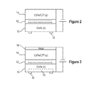
- FIG. 2 shows a cross-section of a first example of a device made in accordance with the present invention.
- FIG. 3 shows a cross-section of a second example of a device made in accordance with the present invention.
- a suitable substrate is a semiconductor substrate of gallium arsenide or silicon 10 .
- This substrate can be processed in accordance with normal semiconductor fabrication techniques, such as doping using ion implantation, diffusion or lithography and the formation of metal contact regions 16 to create an application-specific integrated circuit (ASIC).
- ASIC application-specific integrated circuit
- the circuit will be designed so that electrical signals generated as a result of the absorption of photons in a crystal material can be suitably processed, for example to provide an indication of the number or energy level of the photons absorbed, or to provide other information relating to the detected photons.
- the circuit may include pre-amplification, filtering, shaping, thresholding and/or discriminating elements.
- a bulk single crystal material 14 such as a cadmium telluride or cadmium zinc telluride layer which is to act to detect the incident photons, is grown on the semiconductor substrate. It will be appreciated that the bulk single crystal material may be formed on the substrate prior to formation of the electronic circuit in the substrate, with the electronic circuit being formed in the substrate after formation of the bulk crystal material on the substrate.
- FIG. 1 A preferred apparatus for the formation of the bulk single crystal material on the substrate is shown in FIG. 1 .
- the apparatus comprises an evacuated U-tube in the form of a quartz envelope 20 encased in a vacuum jacket 21 .
- Two separate three zone vertical tubular furnaces are provided 22, 23 for the source 24 and the sink zone 25 respectively.
- the source and sink zones are connected by an optically heated horizontal cross member 27 forming a passage 26 .
- a flow restrictor 28 which may comprise a capillary or sintered quartz disk—is provided in the passage 26 .
- the passage comprises two separate points of deviation, in each case at an angle of 90°, providing respective junctions between diverging passages for in-situ monitoring and vapour transport from the source to the sink zone. Windows allowing optical access to source and sink respectively are provided.
- the temperature of the surface of growing crystal in the sink zone can be monitored by a pyrometer or other optical diagnostic apparatus ( 33 ′) located external to the vacuum jacket and in optical communication with the surface of the growing crystal.
- the diagnostic apparatus is in communication with a suitable control system to vary the sink zone temperature.
- the apparatus also comprises means for in-situ monitoring of vapour pressure by access ports 33 to 36 in the region of the flow restrictor 28 , through which vapour pressure monitoring lamps and optics may be directed from a position external to the vacuum jacket with detectors located as shown at a location 35 , 36 diametrically opposed with respect to the passage for vapour transport 26 . These are suitably linked to a control system providing for process control.
- the source tube, growth tube and cross member, in which transport takes place, are fabricated from quartz and the system is demountable with ground glass joints between the cross member and the two vertical tubes allowing removal of grown crystals and replenishment of source material.
- Radiation shields (not shown for clarity) together with the vacuum jacket which surrounds the entire system provide thermal insulation.
- the substrate 10 is located on a quartz block in the growth tube with the gap between this glass block and the quartz envelope forming a downstream flow restrictor. Provision is made for a gas inlet to the source tube and the growth tube may be pumped by a separate pumping system or by connection to the vacuum jacket via a cool dump tube.
- interfacial layers or regions 12 on the substrate 10 onto which the detector material 14 can be deposited.
- the materials for adjacent layers or regions are selected to ensure mismatches between the layers are minimised.
- This lattice parameter is sufficiently close to that of the underlying silicon substrate that any lattice mismatch is minimised.
- the source material supplied to the growth chamber may be gradually altered so as to deposit a gallium arsenide intermediate layer.
- lattice mismatches are one consideration for selecting materials for the interfacial region 12 , other factors such as relative thermal expansion and electron tunnelling/charge transportation may also be important.
- the growth parameters are controlled such that the transitional region has a minimal thickness.
- the growth parameters can be adjusted so that the bulk crystal material can be deposited at a higher rate.
- a bulk cadmium zinc telluride layer is formed on a silicon substrate.
- the silicon substrate is first treated to remove any oxides. This treatment may include chemical etching or heating the substrate to a high temperature in an ultra high vacuum.
- the silicon substrate is provided in the growth chamber, with separate sources of zinc telluride and cadmium telluride.
- the preferred temperature for the growth of the crystal material is around 700° C., and accordingly the temperature of the silicon substrate is increased to this temperature.
- the temperature of the zinc telluride and cadmium telluride sources is then increased at a rate of about 2° C. per minute until the temperature of these reaches the same temperature as that of the substrate. Thereafter, the temperature of the cadmium telluride source is maintained at this level, whilst the temperature of the zinc telluride source is increased at the same rate to a temperature of around 870° C.
- the zinc telluride source reaches a temperature of around 870° C.
- the temperatures of the substrate and source materials are maintained for around 5 hours. This causes the growth of an intermediate layer of zinc telluride to a thickness of around 50 microns on the substrate.
- the temperature of the substrate is maintained at around 700° C. and the temperature of the zinc telluride source is maintained at around 870° C. whilst the temperature of the cadmium telluride source is increased to the same temperature as the zinc telluride source material at a rate of around 2° C. per minute.
- the material layer grown on the substrate will gradually change composition from the zinc telluride material of the intermediate layer to a cadmium zinc telluride material with about 4% zinc.
- the resulting transition region will have a thickness of around 100 microns.
- the transition region could be reduced in thickness by increasing the rate of temperature increase of the cadmium telluride source, or could be made thicker by decreasing the rate of temperature increase.
- bulk crystal cadmium zinc telluride material will be deposited whilst the temperatures of the source materials are held at a higher temperature than the substrate. The precise composition of the deposited bulk crystal material can be controlled by varying the relative temperature of the two source materials.
- FIG. 2 One example of a device formed according to the present invention is shown in FIG. 2 .
- electrical terminals or pads 16 are formed on the substrate 10 for electrical connection to other apparatus, for example to display apparatus.
- the electrical connections 16 can be formed by conventional techniques such as printing, sputtering or lithography.
- the substrate 10 , interfacial region 12 and bulk crystal material 14 form a p-i-n heterostructure. It will be appreciated that the junction can result in amplification of the generated electrons where the reverse bias is such as to create avalanche multiplication.
- FIG. 3 shows an alternative example of the present invention in which a metal layer 18 is formed on the bulk crystal detecting layer 14 .
- the resulting metal—bulk crystal—substrate structure will result in high energy electrons being injected over or tunneling through the layer.
- the photons from the radiation will be absorbed by the dense crystal material.
- the absorption of the photons converts these in to electrical signals which pass through the interfacial region 12 to the underlying semiconductor substrate detained there.
- the electrical signals received by the semiconductor substrate 10 are processed by the integrated circuit formed within the semiconductor substrate 10 .
- Electronic circuit 15 including an application-specific integrated circuit, is positioned between electrical connections 16 .
- a radiation detector By forming a radiation detector by depositing the bulk single crystal material that acts to absorb the incident radiation directly onto the substrate including electronic circuitry that processes the electrons and/or holes generated within the bulk crystal material when the radiation is absorbed, much more accurate detection of the incident radiation is possible than where the electronic circuitry and detector material are formed separately and then joined together.
- the required thickness of the material will be dependent upon the energy to be absorbed.
- the thickness of material required for absorption of radiation of various energies is as set out below:
Abstract
Description
| Thickness required for 50% | |||
| | absorption | ||
| 30 | keV | 0.007 | cm | ||
| 100 | keV | 0.07 | cm | ||
| 200 | keV | 0.35 | cm | ||
| 500 | keV | 1.2 | cm | ||
| 750 | keV | 1.7 | cm | ||
| 1-10 | MeV | 2.3-3.5 | cm | ||
Claims (8)
Priority Applications (1)
| Application Number | Priority Date | Filing Date | Title |
|---|---|---|---|
| US12/880,458 US8093671B2 (en) | 2005-12-21 | 2010-09-13 | Semiconductor device with a bulk single crystal on a substrate |
Applications Claiming Priority (5)
| Application Number | Priority Date | Filing Date | Title |
|---|---|---|---|
| GB0526072.4 | 2005-12-21 | ||
| GB0526072A GB2433648A (en) | 2005-12-21 | 2005-12-21 | Radiation detector formed by deposition of bulk semiconductor crystal layers |
| PCT/GB2006/004868 WO2007072024A1 (en) | 2005-12-21 | 2006-12-21 | Semiconductor device with a bulk single crystal on a substrate |
| US15811108A | 2008-08-01 | 2008-08-01 | |
| US12/880,458 US8093671B2 (en) | 2005-12-21 | 2010-09-13 | Semiconductor device with a bulk single crystal on a substrate |
Related Parent Applications (3)
| Application Number | Title | Priority Date | Filing Date |
|---|---|---|---|
| PCT/GB2006/004868 Division WO2007072024A1 (en) | 2005-12-21 | 2006-12-21 | Semiconductor device with a bulk single crystal on a substrate |
| US12/158,111 Division US8093095B2 (en) | 2005-12-21 | 2006-12-21 | Semiconductor device with a bulk single crystal on a substrate |
| US15811108A Division | 2005-12-21 | 2008-08-01 |
Publications (2)
| Publication Number | Publication Date |
|---|---|
| US20100327277A1 US20100327277A1 (en) | 2010-12-30 |
| US8093671B2 true US8093671B2 (en) | 2012-01-10 |
Family
ID=35840924
Family Applications (2)
| Application Number | Title | Priority Date | Filing Date |
|---|---|---|---|
| US12/158,111 Active 2027-09-29 US8093095B2 (en) | 2005-12-21 | 2006-12-21 | Semiconductor device with a bulk single crystal on a substrate |
| US12/880,458 Active US8093671B2 (en) | 2005-12-21 | 2010-09-13 | Semiconductor device with a bulk single crystal on a substrate |
Family Applications Before (1)
| Application Number | Title | Priority Date | Filing Date |
|---|---|---|---|
| US12/158,111 Active 2027-09-29 US8093095B2 (en) | 2005-12-21 | 2006-12-21 | Semiconductor device with a bulk single crystal on a substrate |
Country Status (5)
| Country | Link |
|---|---|
| US (2) | US8093095B2 (en) |
| EP (1) | EP1969645A1 (en) |
| JP (1) | JP5437637B2 (en) |
| GB (1) | GB2433648A (en) |
| WO (1) | WO2007072024A1 (en) |
Families Citing this family (6)
| Publication number | Priority date | Publication date | Assignee | Title |
|---|---|---|---|---|
| JP5662001B2 (en) * | 2005-12-21 | 2015-01-28 | クロメック リミテッド | Semiconductor device and manufacturing method thereof |
| GB2433648A (en) * | 2005-12-21 | 2007-06-27 | Durham Scient Crystals Ltd | Radiation detector formed by deposition of bulk semiconductor crystal layers |
| EP2088451B1 (en) * | 2008-02-05 | 2016-01-06 | PANalytical B.V. | Imaging detector |
| KR102125277B1 (en) | 2012-06-26 | 2020-06-22 | 삼성전자주식회사 | Optical integrated circuits, semiconductor devices including the same, and methods of manufacturing the same |
| WO2018201308A1 (en) * | 2017-05-03 | 2018-11-08 | Shenzhen Xpectvision Technology Co., Ltd. | Method of making radiation detector |
| CN112133775B (en) * | 2020-09-04 | 2022-11-08 | 上海大学 | Cadmium zinc telluride/silicon gamma ray X-ray detector and preparation method thereof |
Citations (39)
| Publication number | Priority date | Publication date | Assignee | Title |
|---|---|---|---|---|
| JPS61205693A (en) | 1985-03-07 | 1986-09-11 | Nec Corp | Crystal growth |
| US4689650A (en) | 1985-10-03 | 1987-08-25 | The United States Of America As Represented By The Secretary Of The Army | Infrared epitaxial detector structure and method of making same |
| US4699688A (en) | 1986-07-14 | 1987-10-13 | Gte Laboratories Incorporated | Method of epitaxially growing gallium arsenide on silicon |
| US4710794A (en) | 1985-02-13 | 1987-12-01 | Kabushiki Kaisha Toshiba | Composite semiconductor device |
| FR2612335A1 (en) | 1987-03-12 | 1988-09-16 | Telecommunications Sa | HgCdTe photodiode with fast response |
| US4826784A (en) | 1987-11-13 | 1989-05-02 | Kopin Corporation | Selective OMCVD growth of compound semiconductor materials on silicon substrates |
| EP0343738A2 (en) | 1988-05-27 | 1989-11-29 | Philips Electronics Uk Limited | Manufacture of electronic devices comprising cadmium mercury telluride with silicon-on-sapphire circuitry |
| US4965649A (en) | 1988-12-23 | 1990-10-23 | Ford Aerospace Corporation | Manufacture of monolithic infrared focal plane arrays |
| US4970567A (en) | 1987-11-23 | 1990-11-13 | Santa Barbara Research Center | Method and apparatus for detecting infrared radiation |
| JPH05315582A (en) | 1992-05-07 | 1993-11-26 | Fujitsu Ltd | Infrared detector |
| US5306386A (en) | 1993-04-06 | 1994-04-26 | Hughes Aircraft Company | Arsenic passivation for epitaxial deposition of ternary chalcogenide semiconductor films onto silicon substrates |
| US5389792A (en) | 1993-01-04 | 1995-02-14 | Grumman Aerospace Corporation | Electron microprobe utilizing thermal detector arrays |
| WO1995031824A1 (en) | 1994-05-16 | 1995-11-23 | Santa Barbara Research Center | Multilayer buffer structure including ii-vi compounds on a silicon substrate |
| US5581117A (en) | 1994-12-13 | 1996-12-03 | Nec Corporation | Si base substrate covered by a CdTe or Cd-rich CdZnTe layer |
| DE19711849A1 (en) | 1997-03-21 | 1998-09-24 | Luebelsmeyer Klaus Prof Dr | X=ray detector with semi-insulating semiconductor substrate |
| US5814149A (en) | 1994-11-25 | 1998-09-29 | Kabushiki Kaisha Kobe Seiko Sho | Methods for manufacturing monocrystalline diamond films |
| US5838053A (en) | 1996-09-19 | 1998-11-17 | Raytheon Ti Systems, Inc. | Method of forming a cadmium telluride/silicon structure |
| US5861626A (en) | 1996-04-04 | 1999-01-19 | Raytheon Ti System, Inc. | Mercury cadmium telluride infrared filters and detectors and methods of fabrication |
| US6127203A (en) | 1996-08-30 | 2000-10-03 | Drs Technologies, Inc. | Thermoplastic mounting of a semiconductor die to a substrate having a mismatched coefficient of thermal expansion |
| JP2001200366A (en) | 1999-12-30 | 2001-07-24 | Samsung Electro Mech Co Ltd | Method for producing crack-free gallium nitride thick film by hydride vapor phase epitaxial growth method |
| US6281039B1 (en) | 1998-09-28 | 2001-08-28 | Commissariat A L'energie Atomique | Hybrid device and a method of producing electrically active components by an assembly operation |
| US20020028564A1 (en) | 2000-07-10 | 2002-03-07 | Kensaku Motoki | Method of producing a single crystal gallium nitride substrate and single crystal gallium nitride substrate |
| EP1019568B1 (en) | 1997-08-22 | 2002-06-05 | University Of Durham | Apparatus and process for crystal growth |
| WO2002044443A1 (en) | 2000-11-30 | 2002-06-06 | North Carolina State University | Methods and apparatus for producing m'n based materials |
| WO2002067014A1 (en) | 2001-02-18 | 2002-08-29 | Real-Time Radiography Ltd. | Wide band gap semiconductor composite detector plates for x-ray digital radiography |
| US20030024471A1 (en) | 2001-08-06 | 2003-02-06 | Motorola, Inc. | Fabrication of semiconductor structures and devices forms by utilizing laser assisted deposition |
| US20030034500A1 (en) | 2001-08-15 | 2003-02-20 | Motorola, Inc. | Semiconductor structure including a zintl material buffer layer, device including the structure, and method of forming the structure and device |
| US20030049898A1 (en) | 1997-11-18 | 2003-03-13 | Sergey Karpov | Method for fabricating a P-N heterojunction device utilizing HVPE grown III-V compound layers and resultant device |
| US6733591B2 (en) | 1998-06-18 | 2004-05-11 | University Of Florida Research Foundation, Inc. | Method and apparatus for producing group-III nitrides |
| FR2852146A1 (en) | 2003-03-04 | 2004-09-10 | Univ Paris Curie | Imager with direct conversion of photons to electrons, incorporating an epitaxial layer, for the detection of X rays for medical and industrial applications such as luggage examination at airports |
| US20040183023A1 (en) | 2001-03-12 | 2004-09-23 | Kyo-Seop Choo | X-ray detector and method of fabricating therefore |
| WO2005053038A1 (en) | 2003-11-27 | 2005-06-09 | Nagoya Industrial Science Research Institute | Semiconductor radiation detector and process for producing the same |
| WO2005060011A1 (en) | 2003-12-16 | 2005-06-30 | National University Corporation Shizuoka University | Wide range energy radiation detector and manufacturing method |
| US20050183658A1 (en) | 2001-10-09 | 2005-08-25 | Sumitomo Electric Industries, Ltd. | AlxInyGa1-x-yN mixture crystal substrate, method of growing AlxInyGa1-x-yN mixture crystal substrate and method of producing AlxInyGa1-x-yN mixture crystal substrate |
| US20050247260A1 (en) | 2004-05-07 | 2005-11-10 | Hyunmin Shin | Non-polar single crystalline a-plane nitride semiconductor wafer and preparation thereof |
| US20060011135A1 (en) | 2001-07-06 | 2006-01-19 | Dmitriev Vladimir A | HVPE apparatus for simultaneously producing multiple wafers during a single epitaxial growth run |
| US7289336B2 (en) * | 2004-10-28 | 2007-10-30 | General Electric Company | Electronic packaging and method of making the same |
| US20080315342A1 (en) | 2005-12-21 | 2008-12-25 | Durham Scientific Crystals Limited | Semiconductor Device with a Bulk Single Crystal on a Substrate |
| US20090053453A1 (en) | 2005-12-21 | 2009-02-26 | Durham Scientific Crystals Limited | Semiconductor device and method of manufacture thereof |
Family Cites Families (9)
| Publication number | Priority date | Publication date | Assignee | Title |
|---|---|---|---|---|
| US581626A (en) * | 1897-04-27 | smith | ||
| DE3883526T2 (en) * | 1987-11-23 | 1994-03-03 | Santa Barbara Res Center | METHOD AND DEVICE FOR DETECTING INFRARED RADIATION. |
| JPH05218377A (en) * | 1992-02-05 | 1993-08-27 | Mitsubishi Electric Corp | Semiconductor photodetector |
| US5373182A (en) * | 1993-01-12 | 1994-12-13 | Santa Barbara Research Center | Integrated IR and visible detector |
| JPH07335929A (en) * | 1994-06-03 | 1995-12-22 | Fujitsu Ltd | Semiconductor photodetector |
| JPH088453A (en) * | 1994-06-17 | 1996-01-12 | Fujitsu Ltd | Infrared detector |
| JP3932857B2 (en) * | 2001-10-22 | 2007-06-20 | 株式会社島津製作所 | Radiation detector |
| JP4388899B2 (en) * | 2002-11-19 | 2009-12-24 | コーニンクレッカ フィリップス エレクトロニクス エヌ ヴィ | X-ray inspection equipment |
| US6969646B2 (en) * | 2003-02-10 | 2005-11-29 | Chartered Semiconductor Manufacturing Ltd. | Method of activating polysilicon gate structure dopants after offset spacer deposition |
-
2005
- 2005-12-21 GB GB0526072A patent/GB2433648A/en not_active Withdrawn
-
2006
- 2006-12-21 EP EP06831440A patent/EP1969645A1/en not_active Ceased
- 2006-12-21 WO PCT/GB2006/004868 patent/WO2007072024A1/en active Application Filing
- 2006-12-21 US US12/158,111 patent/US8093095B2/en active Active
- 2006-12-21 JP JP2008546619A patent/JP5437637B2/en active Active
-
2010
- 2010-09-13 US US12/880,458 patent/US8093671B2/en active Active
Patent Citations (44)
| Publication number | Priority date | Publication date | Assignee | Title |
|---|---|---|---|---|
| US4710794A (en) | 1985-02-13 | 1987-12-01 | Kabushiki Kaisha Toshiba | Composite semiconductor device |
| JPS61205693A (en) | 1985-03-07 | 1986-09-11 | Nec Corp | Crystal growth |
| US4689650A (en) | 1985-10-03 | 1987-08-25 | The United States Of America As Represented By The Secretary Of The Army | Infrared epitaxial detector structure and method of making same |
| US4699688A (en) | 1986-07-14 | 1987-10-13 | Gte Laboratories Incorporated | Method of epitaxially growing gallium arsenide on silicon |
| FR2612335A1 (en) | 1987-03-12 | 1988-09-16 | Telecommunications Sa | HgCdTe photodiode with fast response |
| US4826784A (en) | 1987-11-13 | 1989-05-02 | Kopin Corporation | Selective OMCVD growth of compound semiconductor materials on silicon substrates |
| US4970567A (en) | 1987-11-23 | 1990-11-13 | Santa Barbara Research Center | Method and apparatus for detecting infrared radiation |
| EP0343738A2 (en) | 1988-05-27 | 1989-11-29 | Philips Electronics Uk Limited | Manufacture of electronic devices comprising cadmium mercury telluride with silicon-on-sapphire circuitry |
| US4965649A (en) | 1988-12-23 | 1990-10-23 | Ford Aerospace Corporation | Manufacture of monolithic infrared focal plane arrays |
| JPH05315582A (en) | 1992-05-07 | 1993-11-26 | Fujitsu Ltd | Infrared detector |
| US5389792A (en) | 1993-01-04 | 1995-02-14 | Grumman Aerospace Corporation | Electron microprobe utilizing thermal detector arrays |
| US5306386A (en) | 1993-04-06 | 1994-04-26 | Hughes Aircraft Company | Arsenic passivation for epitaxial deposition of ternary chalcogenide semiconductor films onto silicon substrates |
| WO1995031824A1 (en) | 1994-05-16 | 1995-11-23 | Santa Barbara Research Center | Multilayer buffer structure including ii-vi compounds on a silicon substrate |
| US5814149A (en) | 1994-11-25 | 1998-09-29 | Kabushiki Kaisha Kobe Seiko Sho | Methods for manufacturing monocrystalline diamond films |
| US5581117A (en) | 1994-12-13 | 1996-12-03 | Nec Corporation | Si base substrate covered by a CdTe or Cd-rich CdZnTe layer |
| US5861626A (en) | 1996-04-04 | 1999-01-19 | Raytheon Ti System, Inc. | Mercury cadmium telluride infrared filters and detectors and methods of fabrication |
| US6127203A (en) | 1996-08-30 | 2000-10-03 | Drs Technologies, Inc. | Thermoplastic mounting of a semiconductor die to a substrate having a mismatched coefficient of thermal expansion |
| US5838053A (en) | 1996-09-19 | 1998-11-17 | Raytheon Ti Systems, Inc. | Method of forming a cadmium telluride/silicon structure |
| DE19711849A1 (en) | 1997-03-21 | 1998-09-24 | Luebelsmeyer Klaus Prof Dr | X=ray detector with semi-insulating semiconductor substrate |
| EP1019568B1 (en) | 1997-08-22 | 2002-06-05 | University Of Durham | Apparatus and process for crystal growth |
| US6890809B2 (en) | 1997-11-18 | 2005-05-10 | Technologies And Deviles International, Inc. | Method for fabricating a P-N heterojunction device utilizing HVPE grown III-V compound layers and resultant device |
| US20030049898A1 (en) | 1997-11-18 | 2003-03-13 | Sergey Karpov | Method for fabricating a P-N heterojunction device utilizing HVPE grown III-V compound layers and resultant device |
| US6733591B2 (en) | 1998-06-18 | 2004-05-11 | University Of Florida Research Foundation, Inc. | Method and apparatus for producing group-III nitrides |
| US6281039B1 (en) | 1998-09-28 | 2001-08-28 | Commissariat A L'energie Atomique | Hybrid device and a method of producing electrically active components by an assembly operation |
| JP2001200366A (en) | 1999-12-30 | 2001-07-24 | Samsung Electro Mech Co Ltd | Method for producing crack-free gallium nitride thick film by hydride vapor phase epitaxial growth method |
| US6468882B2 (en) | 2000-07-10 | 2002-10-22 | Sumitomo Electric Industries, Ltd. | Method of producing a single crystal gallium nitride substrate and single crystal gallium nitride substrate |
| US20020028564A1 (en) | 2000-07-10 | 2002-03-07 | Kensaku Motoki | Method of producing a single crystal gallium nitride substrate and single crystal gallium nitride substrate |
| WO2002044443A1 (en) | 2000-11-30 | 2002-06-06 | North Carolina State University | Methods and apparatus for producing m'n based materials |
| US6784085B2 (en) | 2000-11-30 | 2004-08-31 | North Carolina State University | MIIIN based materials and methods and apparatus for producing same |
| WO2002067014A1 (en) | 2001-02-18 | 2002-08-29 | Real-Time Radiography Ltd. | Wide band gap semiconductor composite detector plates for x-ray digital radiography |
| US6906331B2 (en) | 2001-03-12 | 2005-06-14 | Lg. Philips Lcd Co., Ltd. | X-ray detector and method of fabricating therefore |
| US20040183023A1 (en) | 2001-03-12 | 2004-09-23 | Kyo-Seop Choo | X-ray detector and method of fabricating therefore |
| US20060011135A1 (en) | 2001-07-06 | 2006-01-19 | Dmitriev Vladimir A | HVPE apparatus for simultaneously producing multiple wafers during a single epitaxial growth run |
| US20030024471A1 (en) | 2001-08-06 | 2003-02-06 | Motorola, Inc. | Fabrication of semiconductor structures and devices forms by utilizing laser assisted deposition |
| US20030034500A1 (en) | 2001-08-15 | 2003-02-20 | Motorola, Inc. | Semiconductor structure including a zintl material buffer layer, device including the structure, and method of forming the structure and device |
| US20050183658A1 (en) | 2001-10-09 | 2005-08-25 | Sumitomo Electric Industries, Ltd. | AlxInyGa1-x-yN mixture crystal substrate, method of growing AlxInyGa1-x-yN mixture crystal substrate and method of producing AlxInyGa1-x-yN mixture crystal substrate |
| FR2852146A1 (en) | 2003-03-04 | 2004-09-10 | Univ Paris Curie | Imager with direct conversion of photons to electrons, incorporating an epitaxial layer, for the detection of X rays for medical and industrial applications such as luggage examination at airports |
| WO2005053038A1 (en) | 2003-11-27 | 2005-06-09 | Nagoya Industrial Science Research Institute | Semiconductor radiation detector and process for producing the same |
| EP1691422A1 (en) | 2003-11-27 | 2006-08-16 | Nagoya Industrial Science Research Institute | Semiconductor radiation detector and process for producing the same |
| WO2005060011A1 (en) | 2003-12-16 | 2005-06-30 | National University Corporation Shizuoka University | Wide range energy radiation detector and manufacturing method |
| US20050247260A1 (en) | 2004-05-07 | 2005-11-10 | Hyunmin Shin | Non-polar single crystalline a-plane nitride semiconductor wafer and preparation thereof |
| US7289336B2 (en) * | 2004-10-28 | 2007-10-30 | General Electric Company | Electronic packaging and method of making the same |
| US20080315342A1 (en) | 2005-12-21 | 2008-12-25 | Durham Scientific Crystals Limited | Semiconductor Device with a Bulk Single Crystal on a Substrate |
| US20090053453A1 (en) | 2005-12-21 | 2009-02-26 | Durham Scientific Crystals Limited | Semiconductor device and method of manufacture thereof |
Non-Patent Citations (19)
| Title |
|---|
| Abstract for DE 197 11 849 A1 (1 page). |
| Abstract for FR 2 612 335 A1 (1 page). |
| Abstract for FR 2 852 146 A1 (1 page). |
| Abstract for JP 2001200366 A (1 page). |
| Abstract for JP 5315582 A (1 page). |
| Abstract for JP 61205693 A (1 page). |
| Abstract for WO 2005/053038 A1 (1 page). |
| Abstract for WO 2005/060011 A1 (1 page). |
| Bhat et al., "Growth of (100) Oriented CdTe on Si Using Ge as a Buffer Layer," Appl. Phys. Lett., 64(5):566-568 (1994). |
| Blue, M.D., "Optical Absorption in HgTe and HgCdTe," Physical Review, vol. 134, No. 1A, A226-A234 (1964). |
| Hong et al., "Growth and Photoconductor Properties of HgCdTe Epilayers Grown by Hot Wall Epitaxy Method," Journal of Crystal Growth, 240(1-2):135-141 (2002). |
| Kim et al., "Structural and Optical Properties of a Strained CdTe/GaAs Heterostructure Grown by Temperature-Gradient Vapor Transport Deposition at Low Temperature," Thin Solid Films, 259(2):253-258 (1995). |
| Lalev et al., "Hot Wall Epitaxy of High-Quality CdTe/Si(111)," Journal of Crystal Growth, 256(1-2):20-26 (2003). |
| Leo et al., "Influence of a ZnTe Buffer Layer on the Structural Quality of CdTe Epilayers Grown on (100) GaAs by Metalorganic Vapor Phase Epitaxy," J. Vac. Sci. Technology B, 14(3):1739-1744 (May/Jun. 1996). |
| Mar. 30, 2006 UK Search Report for Patent Application No. GB0526073.2 (1 page). |
| May 11, 2006 UK Search Report for Patent Application No. GB0526070.8 (1 page). |
| May 31, 2006 UK Search Report for Patent Application No. GB0526072.4 (1 page). |
| May 31, 2006 UK Search Report for Patent Application No. GB0526075.7 (1 page). |
| Rujirawat et al., "High Quality Large-Area CdTe(211)B on Si(211) Grown by Molecular Beam Epitaxy," Appl. Phys. Lett., 71(13):1810-1812 (1997). |
Also Published As
| Publication number | Publication date |
|---|---|
| GB2433648A (en) | 2007-06-27 |
| EP1969645A1 (en) | 2008-09-17 |
| US20080315342A1 (en) | 2008-12-25 |
| JP2009521121A (en) | 2009-05-28 |
| US8093095B2 (en) | 2012-01-10 |
| WO2007072024A1 (en) | 2007-06-28 |
| GB0526072D0 (en) | 2006-02-01 |
| JP5437637B2 (en) | 2014-03-12 |
| US20100327277A1 (en) | 2010-12-30 |
Similar Documents
| Publication | Publication Date | Title |
|---|---|---|
| US8093671B2 (en) | Semiconductor device with a bulk single crystal on a substrate | |
| Burke et al. | Soft-X-ray CCD imagers for AXAF | |
| EP0177918B1 (en) | Uv detector and method for fabricating it | |
| EP1969622B1 (en) | Semiconductor device and method of manufacture thereof | |
| US8237126B2 (en) | X-ray imaging device and method for the manufacturing thereof | |
| US7301155B2 (en) | Radiation detector and radiation imaging apparatus and method for producing radiation detector | |
| US20030160172A1 (en) | Multispectral monolithic infrared focal plane array detectors | |
| Moser | Silicon detector systems in high energy physics | |
| EP2162924B1 (en) | Semiconductor device structure and method of manufacture thereof | |
| JPH06350068A (en) | Manufacture of semiconductor energy ray detector | |
| US8871552B2 (en) | Method of manufacturing radiation detector | |
| US20220115554A1 (en) | Apparatuses for detecting radiation and their methods of making | |
| WO2007072021A1 (en) | Semiconductor device structure and method of manufacture thereof | |
| Chiodini | Diamond particle detectors for high energy physics | |
| JP5621919B2 (en) | Radiation detector manufacturing method and radiation detector | |
| CN116914000B (en) | Top-doped planar light guide type non-flip bonding quantum dot imaging chip | |
| EP0345343A1 (en) | Method and apparatus for detecting infrared radiation | |
| Owens et al. | GaAs arrays for X-ray spectroscopy | |
| Kim et al. | Visible-blind ultraviolet imagers consisting of 8× 8 AlGaN pin photodiode arrays | |
| Olschner et al. | Silicon-drift photodiodes for gamma-ray scintillator photodetection | |
| JPH02205074A (en) | Infrared ray detector | |
| JPH10190020A (en) | Infrared ray detector and method for manufacturing and driving it | |
| WO2003090445A2 (en) | Wide bandgap digital radiation imaging array |
Legal Events
| Date | Code | Title | Description |
|---|---|---|---|
| AS | Assignment |
Owner name: DURHAM SCIENTIFIC CRYSTALS LIMITED, UNITED KINGDOM Free format text: ASSIGNMENT OF ASSIGNORS INTEREST;ASSIGNORS:BASU, ARNAB;ROBINSON, MAX;CANTWELL, BEN;AND OTHERS;SIGNING DATES FROM 20080722 TO 20080724;REEL/FRAME:024976/0854 |
|
| AS | Assignment |
Owner name: KROMEK LIMITED, UNITED KINGDOM Free format text: CHANGE OF NAME;ASSIGNOR:DURHAM SCIENTIFIC CRYSTALS LIMITED;REEL/FRAME:025946/0739 Effective date: 20100604 |
|
| STCF | Information on status: patent grant |
Free format text: PATENTED CASE |
|
| FPAY | Fee payment |
Year of fee payment: 4 |
|
| FEPP | Fee payment procedure |
Free format text: MAINTENANCE FEE REMINDER MAILED (ORIGINAL EVENT CODE: REM.); ENTITY STATUS OF PATENT OWNER: LARGE ENTITY |
|
| FEPP | Fee payment procedure |
Free format text: 7.5 YR SURCHARGE - LATE PMT W/IN 6 MO, LARGE ENTITY (ORIGINAL EVENT CODE: M1555); ENTITY STATUS OF PATENT OWNER: LARGE ENTITY |
|
| MAFP | Maintenance fee payment |
Free format text: PAYMENT OF MAINTENANCE FEE, 8TH YEAR, LARGE ENTITY (ORIGINAL EVENT CODE: M1552); ENTITY STATUS OF PATENT OWNER: LARGE ENTITY Year of fee payment: 8 |
|
| FEPP | Fee payment procedure |
Free format text: ENTITY STATUS SET TO SMALL (ORIGINAL EVENT CODE: SMAL); ENTITY STATUS OF PATENT OWNER: SMALL ENTITY |
|
| MAFP | Maintenance fee payment |
Free format text: PAYMENT OF MAINTENANCE FEE, 12TH YR, SMALL ENTITY (ORIGINAL EVENT CODE: M2553); ENTITY STATUS OF PATENT OWNER: SMALL ENTITY Year of fee payment: 12 |