US8089425B2 - Optical designs for scanning beam display systems using fluorescent screens - Google Patents
Optical designs for scanning beam display systems using fluorescent screens Download PDFInfo
- Publication number
- US8089425B2 US8089425B2 US11/510,495 US51049506A US8089425B2 US 8089425 B2 US8089425 B2 US 8089425B2 US 51049506 A US51049506 A US 51049506A US 8089425 B2 US8089425 B2 US 8089425B2
- Authority
- US
- United States
- Prior art keywords
- lens
- laser
- screen
- laser beams
- beams
- Prior art date
- Legal status (The legal status is an assumption and is not a legal conclusion. Google has not performed a legal analysis and makes no representation as to the accuracy of the status listed.)
- Expired - Fee Related, expires
Links
- 230000003287 optical effect Effects 0.000 title claims description 90
- 238000013461 design Methods 0.000 title description 35
- 230000005284 excitation Effects 0.000 claims abstract description 48
- 239000000463 material Substances 0.000 claims abstract description 35
- 238000003384 imaging method Methods 0.000 claims description 9
- 238000003491 array Methods 0.000 claims description 7
- 238000004891 communication Methods 0.000 claims description 3
- 238000012634 optical imaging Methods 0.000 claims description 3
- OAICVXFJPJFONN-UHFFFAOYSA-N Phosphorus Chemical compound [P] OAICVXFJPJFONN-UHFFFAOYSA-N 0.000 description 27
- 239000003086 colorant Substances 0.000 description 22
- 238000000034 method Methods 0.000 description 13
- 210000001747 pupil Anatomy 0.000 description 10
- 239000000758 substrate Substances 0.000 description 10
- 238000006073 displacement reaction Methods 0.000 description 9
- 239000002096 quantum dot Substances 0.000 description 8
- 238000012937 correction Methods 0.000 description 5
- 230000003595 spectral effect Effects 0.000 description 5
- 230000007246 mechanism Effects 0.000 description 4
- 230000008901 benefit Effects 0.000 description 3
- 230000008859 change Effects 0.000 description 3
- 150000001875 compounds Chemical class 0.000 description 3
- 230000007423 decrease Effects 0.000 description 3
- 230000006870 function Effects 0.000 description 3
- 239000004973 liquid crystal related substance Substances 0.000 description 3
- 238000013459 approach Methods 0.000 description 2
- 230000000694 effects Effects 0.000 description 2
- 239000010408 film Substances 0.000 description 2
- 239000011159 matrix material Substances 0.000 description 2
- 239000003973 paint Substances 0.000 description 2
- 238000012545 processing Methods 0.000 description 2
- 230000009467 reduction Effects 0.000 description 2
- 230000003252 repetitive effect Effects 0.000 description 2
- 230000004044 response Effects 0.000 description 2
- 239000004065 semiconductor Substances 0.000 description 2
- 238000009987 spinning Methods 0.000 description 2
- 241001507928 Aria Species 0.000 description 1
- 241000870659 Crassula perfoliata var. minor Species 0.000 description 1
- 235000004522 Pentaglottis sempervirens Nutrition 0.000 description 1
- XUIMIQQOPSSXEZ-UHFFFAOYSA-N Silicon Chemical compound [Si] XUIMIQQOPSSXEZ-UHFFFAOYSA-N 0.000 description 1
- 235000004494 Sorbus aria Nutrition 0.000 description 1
- 238000010521 absorption reaction Methods 0.000 description 1
- 230000032683 aging Effects 0.000 description 1
- -1 among others Chemical class 0.000 description 1
- 230000005540 biological transmission Effects 0.000 description 1
- UHYPYGJEEGLRJD-UHFFFAOYSA-N cadmium(2+);selenium(2-) Chemical compound [Se-2].[Cd+2] UHYPYGJEEGLRJD-UHFFFAOYSA-N 0.000 description 1
- 239000004020 conductor Substances 0.000 description 1
- 238000010894 electron beam technology Methods 0.000 description 1
- 238000005516 engineering process Methods 0.000 description 1
- 238000001914 filtration Methods 0.000 description 1
- 239000010437 gem Substances 0.000 description 1
- 229910001751 gemstone Inorganic materials 0.000 description 1
- 239000011521 glass Substances 0.000 description 1
- 239000006193 liquid solution Substances 0.000 description 1
- 238000003754 machining Methods 0.000 description 1
- 239000000203 mixture Substances 0.000 description 1
- RVTZCBVAJQQJTK-UHFFFAOYSA-N oxygen(2-);zirconium(4+) Chemical compound [O-2].[O-2].[Zr+4] RVTZCBVAJQQJTK-UHFFFAOYSA-N 0.000 description 1
- 239000002245 particle Substances 0.000 description 1
- 230000037361 pathway Effects 0.000 description 1
- 239000000843 powder Substances 0.000 description 1
- 230000008569 process Effects 0.000 description 1
- 230000000750 progressive effect Effects 0.000 description 1
- 238000000926 separation method Methods 0.000 description 1
- 238000007493 shaping process Methods 0.000 description 1
- 229910052710 silicon Inorganic materials 0.000 description 1
- 239000010703 silicon Substances 0.000 description 1
- 239000007787 solid Substances 0.000 description 1
- 239000006104 solid solution Substances 0.000 description 1
- 230000003068 static effect Effects 0.000 description 1
- 239000010409 thin film Substances 0.000 description 1
- 238000011144 upstream manufacturing Methods 0.000 description 1
- 230000000007 visual effect Effects 0.000 description 1
Images


Classifications
-
- G—PHYSICS
- G02—OPTICS
- G02B—OPTICAL ELEMENTS, SYSTEMS OR APPARATUS
- G02B26/00—Optical devices or arrangements for the control of light using movable or deformable optical elements
- G02B26/08—Optical devices or arrangements for the control of light using movable or deformable optical elements for controlling the direction of light
- G02B26/10—Scanning systems
- G02B26/105—Scanning systems with one or more pivoting mirrors or galvano-mirrors
-
- G—PHYSICS
- G02—OPTICS
- G02B—OPTICAL ELEMENTS, SYSTEMS OR APPARATUS
- G02B26/00—Optical devices or arrangements for the control of light using movable or deformable optical elements
- G02B26/08—Optical devices or arrangements for the control of light using movable or deformable optical elements for controlling the direction of light
- G02B26/10—Scanning systems
- G02B26/12—Scanning systems using multifaceted mirrors
- G02B26/123—Multibeam scanners, e.g. using multiple light sources or beam splitters
-
- H—ELECTRICITY
- H04—ELECTRIC COMMUNICATION TECHNIQUE
- H04N—PICTORIAL COMMUNICATION, e.g. TELEVISION
- H04N3/00—Scanning details of television systems; Combination thereof with generation of supply voltages
- H04N3/02—Scanning details of television systems; Combination thereof with generation of supply voltages by optical-mechanical means only
- H04N3/08—Scanning details of television systems; Combination thereof with generation of supply voltages by optical-mechanical means only having a moving reflector
-
- H—ELECTRICITY
- H04—ELECTRIC COMMUNICATION TECHNIQUE
- H04N—PICTORIAL COMMUNICATION, e.g. TELEVISION
- H04N9/00—Details of colour television systems
- H04N9/12—Picture reproducers
- H04N9/31—Projection devices for colour picture display, e.g. using electronic spatial light modulators [ESLM]
- H04N9/3129—Projection devices for colour picture display, e.g. using electronic spatial light modulators [ESLM] scanning a light beam on the display screen
-
- H—ELECTRICITY
- H04—ELECTRIC COMMUNICATION TECHNIQUE
- H04N—PICTORIAL COMMUNICATION, e.g. TELEVISION
- H04N9/00—Details of colour television systems
- H04N9/12—Picture reproducers
- H04N9/31—Projection devices for colour picture display, e.g. using electronic spatial light modulators [ESLM]
- H04N9/3141—Constructional details thereof
- H04N9/315—Modulator illumination systems
- H04N9/3164—Modulator illumination systems using multiple light sources
Definitions
- This application relates to display systems that use screens with fluorescent materials to emit colored light under optical excitation, such as laser-based image and video displays and screen designs for such displays.
- projection displays are designed to directly produce color images in different colors, such as red, green and blue and then project the color images on a screen.
- Such systems are often referred to as “projection displays” where the screen is simply a surface to make the color images visible to a viewer.
- projection displays may use white light sources where white beams are filtered and modulated to produce images in red, green and blue colors.
- three light sources in red, green and blue may be used to directly produce three beams in red, green and blue colors and the three beams are modulated to produce images in red, green and blue.
- Examples of such projection displays include digital light processing (DLP) displays, liquid crystal on silicon (LCoS) displays, and grating light valve (GLV) displays.
- DLP digital light processing
- LCDoS liquid crystal on silicon
- GLV grating light valve
- GLV displays use three grating light valves to modulate red, green and blue laser beams, respectively, and use a beam scanner to produce the color images on a screen.
- Another example of laser-based projection displays is described in U.S. Pat. No. 5,920,361 entitled “Methods and apparatus for image projection.”
- Projection displays use optical lens systems to image and project the color images on the screen.
- Some other image and video displays use a “direct” configuration where the screen itself includes light-producing color pixels to directly form color images in the screen.
- Such direct displays eliminate the optical lens systems for projecting the images and therefore can be made relatively smaller than projection displays with the same screen sizes.
- Examples of direct display systems include plasma displays, liquid crystal displays (LCDs), light-emitting-diode (LED) displays (e.g., organic LED displays), and field-emission displays (FEDs).
- Each color pixel in such direct displays includes three adjacent color pixels which produce light in red, green and blue, respectively, by either directly emit colored light as in LED displays and FEDs or by filtering white light such as the LCDs.
- CRT cathode-ray tube
- CRT displays use scanning electron beams in a vacuum tube to excite color phosphors in red, green and blue colors on the screen to emit colored light to produce color images.
- CRT displays can produce vivid colors and bright images with high resolutions, the use of cathode-ray tubes places severe technical limitations on the CRT displays and leads to dramatic decline in demand for CRT displays in recent years.
- the specification of this application describes, among others, scanning beam display systems based on scanning light on a fluorescent screen.
- the screen can include fluorescent materials which emit visible light under excitation of the scanning light to form images with the emitted visible light.
- Multiple lasers can be used to simultaneously scan multiple laser beams to illuminate the screen for enhanced display brightness. For example, the multiple laser beams can illuminate one screen segment at a time and sequentially scan multiple screen segments to complete a full screen.
- one scanning beam display system described in this specification can include lasers forming a laser array to produce a plurality of laser beams, respectively; a scanning module placed in an optical path of the laser beams to scan the laser beams in two orthogonal directions; and an afocal optical relay module placed between the lasers and the scanning module having a plurality of lenses to reduce a spacing between two adjacent laser beams of the laser beam and to overlap the laser beams at the scanning module.
- the optical relay module can include a first lens having a first focal length to receive and focus the laser beams from the lasers; a second lens having a second focal length shorter than the first focal length and spaced from the first lens by the first focal length to focus the laser beams from the first lens; and a third lens having a third focal length longer than the second focal length and spaced from the second lens by the third focal length to focus and direct the laser beams from the second lens to the scanning module.
- the scanning module can include a galvo mirror positioned to receive the laser beams from the third lens and scan the received laser beams along the first scanning direction, and a polygon scanner positioned to receive the laser beams from the galvo mirror and operable to scan the received laser beams along a second scanning direction orthogonal to the first scanning direction, where the system further includes an optical imaging lens module placed between the galvo mirror and the polygon scanner to image the galvo mirror onto the polygon scanner.
- a display system can include lasers forming a laser array to produce a plurality of laser beams, respectively; a scanning module placed in an optical path of the laser beams to scan the laser beams in two orthogonal directions; a screen comprising fluorescent materials that emit visible light to form images with the emitted light when illuminated by the laser beams; a scan lens positioned to receive the laser beams from the scanning module and to project the laser beams onto the screen; and first and second optical reflectors that reflect the laser beams.
- the first optical reflector is positioned to reflect scanning laser beams from the scan lens to the second optical reflector which is positioned to reflect the scanning laser beams from the first optical reflector to the screen, and the first and second optical reflectors are positioned to fold an optical path from the scan lens to the screen to reduce a distance between the scan lens and the screen.
- the specification of this application also describes an example method for scanning light onto a screen to display an image.
- This method includes modulating light to include optical pulses that carry images to be displayed; scanning the light in two orthogonal scanning directions; and using a scan lens to project the scanned light on a screen to show the images, where the light is modulated to carry distorted versions of the images to include image distortions that negate distortions caused by the scan lens when displayed on the screen.
- the timing of the optical pulses in one scanning direction is controlled to negate a portion of distortions caused by the scan lens when displayed on the screen.
- a display system is described to include a light source to produce at least one excitation beam modulated to carry images; a scanning module to scan the excitation beam in two orthogonal directions; a fluorescent screen to receive the scanning excitation beam, the fluorescent screen emitting visible light to form the images with the emitted visible light when illuminated by the scanning excitation beam; and a two-dimensional f-theta scan lens positioned to receive the scanning excitation beam from the scanning module and to project the scanning excitation beam onto the screen.
- This system can also include a signal modulation controller in communication with the light source to supply image data for the images to control the light source which modulates the excitation beam.
- the signal modulation controller provides image data with image distortions which negate optical distortions of the two-dimensional f-theta scan lens when displayed on the screen.
- FIG. 1 shows an example scanning laser display system having a fluorescent screen made of laser-excitable phosphors emitting colored lights under excitation of a scanning laser beam that carries the image information to be displayed.
- FIGS. 2A and 2B show one example screen structure and the structure of color pixels on the screen in FIG. 1 .
- FIG. 2C shows another example for a fluorescent screen with fluorescent stripes formed by placing parallel optical filters over the layer of a uniform fluorescent layer which emits white light under optical excitation.
- FIG. 3 shows an example implementation of the laser module in FIG. 1 having multiple lasers that direct multiple laser beams on the screen.
- FIG. 4 illustrates one example of simultaneous scanning of multiple screen segments with multiple scanning laser beams.
- FIGS. 5A and 5B show an example of a laser module with an array of lasers to produce different scanning beams onto the screen for implementations of the display system in FIG. 3 .
- FIGS. 6 , 7 , 8 and 9 show examples of lasers having laser actuators that control the vertical direction of the laser beam.
- FIG. 10 shows an optical layout of a laser module for implementing the scanning laser module in FIG. 3 .
- FIG. 11 shows an example of a two-dimensional f-theta scan lens with three lens elements.
- FIG. 12 shows an alternative design of an afocal relay in FIG. 10 .
- FIG. 13 shows an example of an afocal relay between a galvo mirror and a polygon scanner to image the galvo mirror on to a reflecting facet of the polygon scanner.
- FIG. 14 illustrates bow distortions caused by a scan lens in a scanning display system based on the laser module in FIG. 3 .
- FIG. 15 shows an example of measured distortions on a screen caused by a scan lens in a scanning system based on the design in FIG. 3 .
- FIGS. 16A and 16B show two examples of folded optical paths for directing a scanning laser beam to a screen with phosphors in scanning beam rear projection systems.
- This application describes scanning beam display systems that use screens with fluorescent materials to emit light under optical excitation to produce images, including laser vector scanner display devices and laser video display devices that use laser excitable fluorescent screens to produce images by absorbing excitation laser light and emitting colored light.
- screen designs with fluorescent materials are described. Screens with phosphor materials under excitation of one or more scanning excitation laser beams are described in detail and are used as specific implementation examples of optically excited fluorescent materials in various system and device examples in this application.
- three different color phosphors that are optically excitable by the laser beam to respectively produce light in red, green, and blue colors suitable for forming color images may be formed on the screen as pixel dots or repetitive red, green and blue phosphor stripes in parallel.
- Various examples described in this application use screens with parallel color phosphor stripes for emitting light in red, green, and blue to illustrate various features of the laser-based displays.
- Phosphor materials are one type of fluorescent materials.
- Various described systems, devices and features in the examples that use phosphors as the fluorescent materials are applicable to displays with screens made of other optically excitable, light-emitting, non-phosphor fluorescent materials.
- quantum dot materials emit light under proper optical excitation and thus can be used as the fluorescent materials for systems and devices in this application.
- semiconductor compounds such as, among others, CdSe and PbS, can be fabricated in form of particles with a diameter on the order of the exciton Bohr radius of the compounds as quantum dot materials to emit light.
- different quantum dot materials with different energy band gap structures may be used to emit different colors under the same excitation light.
- Some quantum dots are between 2 and 10 nanometers in size and include approximately tens of atoms such between 10 to 50 atoms. Quantum dots may be dispersed and mixed in various materials to form liquid solutions, powders, jelly-like matrix materials and solids (e.g., solid solutions).
- Quantum dot films or film stripes may be formed on a substrate as a screen for a system or device in this application.
- three different quantum dot materials can be designed and engineered to be optically excited by the scanning laser beam as the optical pump to produce light in red, green, and blue colors suitable for forming color images.
- Such quantum dots may be formed on the screen as pixel dots arranged in parallel lines (e.g., repetitive sequential red pixel dot line, green pixel dot line and blue pixel dot line).
- Examples of scanning beam display systems described here use at least one scanning laser beam to excite color light-emitting materials deposited on a screen to produce color images.
- the scanning laser beam is modulated to carry images in red, green and blue colors or in other visible colors and is controlled in such a way that the laser beam excites the color light-emitting materials in red, green and blue colors with images in red, green and blue colors, respectively.
- the scanning laser beam carries the images but does not directly produce the visible light seen by a viewer. Instead, the color light-emitting fluorescent materials on the screen absorb the energy of the scanning laser beam and emit visible light in red, green and blue or other colors to generate actual color images seen by the viewer.
- Laser excitation of the fluorescent materials using one or more laser beams with energy sufficient to cause the fluorescent materials to emit light or to luminesce is one of various forms of optical excitation.
- the optical excitation may be generated by a non-laser light source that is sufficiently energetic to excite the fluorescent materials used in the screen.
- non-laser excitation light sources include various light-emitting diodes (LEDs), light lamps and other light sources that produce light at a wavelength or a spectral band to excite a fluorescent material that converts the light of a higher energy into light of lower energy in the visible range.
- the excitation optical beam that excites a fluorescent material on the screen can be at a frequency or in a spectral range that is higher in frequency than the frequency of the emitted visible light by the fluorescent material. Accordingly, the excitation optical beam may be in the violet spectral range and the ultra violet (UV) spectral range, e.g., wavelengths under 420 nm.
- UV light or a UV laser beam is used as an example of the excitation light for a phosphor material or other fluorescent material and may be light at other wavelength.
- FIG. 1 illustrates an example of a laser-based display system using a screen having color phosphor stripes.
- color phosphor dots may also be used to define the image pixels on the screen.
- the system includes a laser module 110 to produce and project at least one scanning laser beam 120 onto a screen 101 .
- the screen 101 has parallel color phosphor stripes in the vertical direction where red phosphor absorbs the laser light to emit light in red, green phosphor absorbs the laser light to emit light in green and blue phosphor absorbs the laser light to emit light in blue. Adjacent three color phosphor stripes are in three different colors. One particular spatial color sequence of the stripes is shown in FIG. 1 as red, green and blue. Other color sequences may also be used.
- the laser beam 120 is at the wavelength within the optical absorption bandwidth of the color phosphors and is usually at a wavelength shorter than the visible blue and the green and red colors for the color images.
- the color phosphors may be phosphors that absorb UV light in the spectral range from about 380 nm to about 420 nm to produce desired red, green and blue light.
- the laser module 110 can include one or more lasers such as UV diode lasers to produce the beam 120 , a beam scanning mechanism to scan the beam 120 horizontally and vertically to render one image frame at a time on the screen 101 , and a signal modulation mechanism to modulate the beam 120 to carry the information for image channels for red, green and blue colors.
- Such display systems may be configured as rear projection systems where the viewer and the laser module 110 are on the opposite sides of the screen 101 .
- such display systems may be configured as front projection systems where the viewer and laser module 110 are on the same side of the screen 101 .
- FIG. 2A shows an exemplary design of the screen 101 in FIG. 1 .
- the screen 101 may include a rear substrate 201 which is transparent to the scanning laser beam 120 and faces the laser module 110 to receive the scanning laser beam 120 .
- a second front substrate 202 is fixed relative to the rear substrate 201 and faces the viewer in a rear projection configuration.
- a color phosphor stripe layer 203 is placed between the substrates 201 and 202 and includes phosphor stripes.
- the color phosphor stripes for emitting red, green and blue colors are represented by “R”, “G” and “B,” respectively.
- the front substrate 202 is transparent to the red, green and blue colors emitted by the phosphor stripes.
- the substrates 201 and 202 may be made of various materials, including glass or plastic panels.
- Each color pixel includes portions of three adjacent color phosphor stripes in the horizontal direction and its vertical dimension is defined by the beam spread of the laser beam 120 in the vertical direction. As such, each color pixel includes three subpixels of three different colors (e.g., the red, green and blue).
- the laser module 110 scans the laser beam 120 one horizontal line at a time, e.g., from left to right and from top to bottom to fill the screen 101 .
- the laser module 110 is fixed in position relative to the screen 101 so that the scanning of the beam 120 can be controlled in a predetermined manner to ensure proper alignment between the laser beam 120 and each pixel position on the screen 101 .
- the scanning laser beam 120 is directed at the green phosphor stripe within a pixel to produce green light for that pixel.
- FIG. 2B further shows the operation of the screen 101 in a view along the direction B-B perpendicular to the surface of the screen 101 . Since each color stripe is longitudinal in shape, the cross section of the beam 120 may be shaped to be elongated along the direction of the stripe to maximize the fill factor of the beam within each color stripe for a pixel. This may be achieved by using a beam shaping optical element in the laser module 110 .
- a laser source that is used to produce a scanning laser beam that excites a phosphor material on the screen may be a single mode laser or a multimode laser.
- the laser may also be a single mode along the direction perpendicular to the elongated direction phosphor stripes to have a small beam spread that is confined by the width of each phosphor stripe. Along the elongated direction of the phosphor stripes, this laser beam may have multiple modes to spread over a larger area than the beam spread in the direction across the phosphor stripe.
- This use of a laser beam with a single mode in one direction to have a small beam footprint on the screen and multiple modes in the perpendicular direction to have a larger footprint on the screen allows the beam to be shaped to fit the elongated color subpixel on the screen and to provide sufficient laser power in the beam via the multimodes to ensure sufficient brightness of the screen.
- FIG. 2C illustrates another example of a fluorescent screen design that has a contiguous and uniform layer 220 of mixed phosphors.
- This mixed phosphor layer 220 is designed and constructed to emit white light under optical excitation of the excitation light 120 .
- the mixed phosphors in the mixed phosphor layer 220 can be designed in various ways and a number of compositions for the mixed phosphors that emit white light are known and documented.
- a layer 210 of color filters such as stripes of red-transmitting, green-transmitting and blue-transmitting filters, is placed on the viewer side of the mixed phosphor layer 220 to filter the white light and to produce colored output light.
- the layers 210 and 220 can be sandwiched between substrates 201 and 202 .
- the color filters may be implemented in various configurations, including in designs similar to the color filters used in color LCD panels.
- each color filter region e.g., a red-transmitting filter
- the filter transmits the red light and absorbs light of other colors including green light and blue light.
- Each filter in the layer 210 may be a multi-layer structure that effectuates a band-pass interference filter with a desired transmission band.
- Various designs and techniques may be used for designing and constructing such filters.
- a fluorescent stripe in the fluorescent screen 101 in various examples described in this application is a fluorescent stripe that emits a designated color under optical excitation and can be either a fluorescent stripe formed of a particular fluorescent material that emits the designed color in FIG. 2A or a combination of a stripe color filter and a white fluorescent layer in FIG. 2C .
- FIG. 3 shows an example implementation of the laser module 110 in FIG. 1 .
- a laser array 310 with multiple lasers is used to generate multiple laser beams 312 to simultaneously scan the screen 101 for enhanced display brightness.
- a signal modulation controller 320 is provided to control and modulate the lasers in the laser array 310 so that the laser beams 312 are modulated to carry the image to be displayed on the screen 101 .
- the signal modulation controller 320 can include a digital image processor that generates digital image signals for the three different color channels and laser driver circuits that produce laser control signals carrying the digital image signals.
- the laser control signals are then applied to modulate the lasers, e.g., the currents for laser diodes, in the laser array 310 .
- the beam scanning is achieved by using a scanning mirror 340 such as a galvo mirror for the vertical scanning and a multi-facet polygon scanner 350 for the horizontal scanning.
- a scan lens 360 is used to project the scanning beams form the polygon scanner 350 onto the screen 101 .
- the scan lens 360 is designed to image each laser in the laser array 310 onto the screen 101 .
- Each of the different reflective facets of the polygon scanner 350 simultaneously scans N horizontal lines where N is the number of lasers.
- the laser beams are first directed to the galvo mirror 340 and then from the galvo mirror 340 to the polygon scanner 350 .
- the output scanning beams 120 are then projected onto the screen 101 .
- a relay optics module 330 is placed in the optical path of the laser beams 312 to modify the spatial property of the laser beams 312 and to produce a closely packed bundle of beams 332 for scanning by the galvo mirror 340 and the polygon scanner 350 as the scanning beams 120 projected onto the screen 101 to excite the phosphors and to generate the images by colored light emitted by the phosphors.
- the laser beams 120 are scanned spatially across the screen 101 to hit different color pixels at different times. Accordingly, each of the modulated beams 120 carries the image signals for the red, green and blue colors for each pixel at different times and for different pixels at different times. Hence, the beams 120 are coded with image information for different pixels at different times by the signal modulation controller 320 .
- the beam scanning thus maps the time-domain coded image signals in the beams 120 onto the spatial pixels on the screen 101 .
- the modulated laser beams 120 can have each color pixel time equally divided into three sequential time slots for the three color subpixels for the three different color channels.
- the modulation of the beams 120 may use pulse modulation techniques to produce desired grey scales in each color, a proper color combination in each pixel, and desired image brightness.
- the multiple beams 120 are directed onto the screen 101 at different and adjacent vertical positions with two adjacent beams being spaced from each other on the screen 101 by one horizontal line of the screen 101 along the vertical direction.
- the beams 120 may not be aligned with each other along the vertical direction on the screen 101 and may be at different positions on the screen 101 along the horizontal direction.
- the beams 120 can only cover one portion of the screen 101 .
- the spinning of the polygon scanner 350 causes the beams 120 from N lasers in the laser array 310 to scan one screen segment of N adjacent horizontal lines on the screen 101 .
- the galvo mirror 340 is adjusted to a different fixed angular position so that the vertical positions of all N beams 120 are adjusted to scan the next adjacent screen segment of N horizontal lines. This process iterates until the entire screen 101 is scanned to produce a full screen display.
- FIG. 4 illustrates the above simultaneous scanning of one screen segment with multiple scanning laser beams at a time and sequentially scanning consecutive screen segments.
- the beams 120 behaves like a paint brush to “paint” one thick horizontal stroke across the screen 101 at a time to cover one screen segment and then subsequently to “paint” another thick horizontal stroke to cover an adjacent vertically shifted screen segment.
- the laser array 310 has 36 lasers
- a 1080-line progressive scan of the screen 101 would require scanning 30 vertical screen segments for a full scan.
- this configuration in an effect divides the screen 101 along the vertical direction into multiple screen segments so that the N scanning beams scan one screen segment at a time with each scanning beam scanning only one line in the screen segment and different beams scanning different sequential lines in that screen segment. After one screen segment is scanned, the N scanning beams are moved at the same time to scan the next adjacent screen segment.
- each scanning laser beam scans only a number of lines across the entire screen along the vertical direction that is equal to the number of screen segments.
- the polygon scanner for the horizontal scanning can operate at a slower speed than a scanning speed needed for a single beam design where the single beam scans every line of the entire screen.
- the number of screen segments decreases as the number of the lasers increases.
- the galvo mirror 340 and the polygon scanner 350 scan 30 lines per frame while a total of 108 lines per frame are scanned when there are only 10 lasers.
- the use of the multiple lasers can increase the image brightness which is approximately proportional to the number of lasers used and, at the same time, can also advantageously reduce the response speeds of the scanning system.
- the vertical beam pointing accuracy is controlled within a threshold in order to produce a high quality image.
- this accuracy in the vertical beam pointing should be controlled to avoid or minimize an overlap between two adjacent screen segments because such an overlap in the vertical direction can severely degrade the image quality.
- the vertical beam pointing accuracy should be less than the width of one horizontal line in implementations.
- This misalignment between two adjacent screen segments can be digitally corrected through modulation of the laser beams 312 by the signal modulation controller 320 .
- Each segment of the screen can be driven with a scan engine capable of generating more horizontal lines than actually required for display in that segment (e.g., 4 extra lines).
- the beam scanning of the system can be configured to have an equal number of extra (unused) lines above and below a segment image for each screen segment. If vertical misalignment exists, the control electronics in the signal modulation controller 320 can shift the segment image upwards or downwards by utilizing these extra lines in place of the normal lines.
- the controller 320 operates to cause each line to move upwards to the previous one, utilizing one of the extra lines above the normal image and adding an extra unused line at the bottom.
- an optical sensor can be used to provide feedback in real time.
- This optical sensor may be a position sensing photodiode located to either side of the viewable area of the screen segment to be controlled. The line would over scan onto this sensor when required.
- an optical beam splitter may be used to provide feedback during the viewable portion of the scan.
- the above described method allows adjustment with a resolution of only one line along the vertical direction.
- the scan engine for scanning the excitation beam can be rotated slightly. This produces slightly diagonal horizontal scan lines.
- the adjacent screen segments would have scan engines slightly rotated on the opposite direction. Under this condition, to create a straight horizontal line, portions of at least two scan lines are used depending on the amount of the rotation. This can produce a less noticeable junction between two neighboring screen segments.
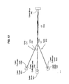
- FIGS. 5A and 5B show an example laser module 500 for a scanning beam display system using an array 310 of lasers 520 to generate multiple scanning beams based the designs in FIGS. 3 and 4 .
- the laser module 500 includes a base 510 on which other components are mounted at predetermined fixed positions.
- a laser tower 510 mounted on one end of the base 501 as the light source for the laser module 500 .
- the laser tower 510 includes a laser array mounting rack 512 that holds multiple lasers 520 of the laser array 310 which produces multiple laser beams and delivers a sufficient amount of total laser power to the fluorescent screen 101 for desired display brightness.
- the laser tower 510 includes a laser tower case 514 that covers part of the laser tower 510 and forms a partial enclosure for holding the laser array mounting rack 512 and the part of optical pathways of the laser beams.
- the laser array mounting rack 512 has a structure to hold lasers 520 at different positions along the vertical direction and different horizontal positions above the base 501 . As illustrated, the lasers 520 can be held in different vertical arrays that are spatially shifted or staggered relative to one another along two orthogonal direction in a plane parallel to the base 501 . For example, one vertical laser array 521 is shown in FIG. 5A and two adjacent staggered vertical laser arrays 521 and 522 are shown in FIG. 5B .
- the lasers 520 in each vertical array are oriented by the design of the laser array mounting rack 512 to direct respective laser beams in a fan configuration as converging beams to point to the galvo mirror 340 mounted on a galvo mirror mount 530 on the base 501 .
- the galvo mirror mount 530 can include a driver circuit for operating and controlling the galvo mirror 350 .
- FIG. 5B shows a bird's eye view of the laser module 500 along the direction B-B as indicated in FIG. 5A .
- the folded beam paths of the laser beams are used to reduce the size of the laser module 500 .
- the lasers 520 are spatially staggered along the laser beam direction to form a three-dimensional array and produce a cone of converging laser beams that are directed to the galvo mirror 340 .
- the staggering arrangement allows two neighboring vertical arrays, e.g., the vertical arrays 521 and 522 , to be spatially close to each other with an array-to-array spacing less than the spacing between two lasers when placed in a common plane.
- the two vertical arrays 521 and 522 are staggered in space to have different distances from the scanning module which includes the galvo mirror 340 and the polygon scanner 350 .
- the converging laser beams are directed through a relay optical module 330 and are transformed into a bundle of closely packed beams before reaching the galvo mirror 340 .
- the galvo mirror 340 scans and reflects the bundle of closely packed beams to the polygon scanner 350 .
- a polygon mount 502 on the base 501 is provided to hold the polygon scanner 350 and includes a motor for spinning the polygon scanner 350 , a power supply and a polygon control circuit.
- a lens mount 550 on the base 501 is used to hold a scan lens assembly 540 to receive the scanning laser beams from the polygon scanner 350 and to project the received scanning beams onto the screen.
- the laser array mounting rack 512 can be designed to hold the lasers 520 at respective positions and orientations so that each laser beam is directed at a proper direction towards the relay optics module 330 and the galvo mirror 340 .
- the laser mounting by the laser array mounting rack 512 is approximate and can deviate from a desired optical alignment for each laser 520 in part due to variations and tolerances in machining of the laser array mounting rack 512 , aging of the structure, thermal fluctuations and other factors.
- the laser module 500 can include one or more mechanisms to control the direction of each laser beam to optically assign each beam for optimized operation.
- FIG. 6 shows an example of each laser 520 with a laser actuator that controls the laser beam direction.
- the laser 520 includes a laser diode or a semiconductor-based laser 610 , a laser collimator 630 that is fixed relative to the laser diode 610 , and a laser position actuator 640 engaged to the assembly of the laser diode 610 and laser collimator 630 .
- the laser diode 610 includes conductor leads 620 that are connected to the laser driver circuit to receive a modulated driver current which generates and modulates the laser beam to carry image data.
- a laser holder 601 is used as a base to hold the above components and to mount the laser 520 to the laser array mounting rack 512 .
- the laser position actuator 640 can be used to tilt the orientation of the assembly of the laser diode 610 and laser collimator 630 relative to the laser holder 601 without changing the relative position or orientation of the laser diode 610 and the laser collimator 630 .
- the tilting of the assembly of the laser diode 610 and laser collimator 630 can be along a single axis, e.g., a horizontal axis parallel to the horizontal rotation axis of the galvo mirror 340 .
- This laser position actuator 640 can be a flexure actuator using a piezoelectric material and can be used for precisely controlling the vertical beam position of each laser beam on the screen.
- FIGS. 7 , 8 and 9 show other designs for controlling the beam pointing.
- Each design includes a beam control actuator at the laser to control the pointing of the beam while the galvo mirror near the polygon is used to control the vertical beam scanning.
- the implementation of this beam control actuator and the above described controls in FIG. 6 allows software control of the static and dynamic beam pointing for each laser.
- a laser 710 such as a diode laser is used to generate the scanning laser beam which may be at a UV or violet wavelength.
- a collimating lens 720 in front of the laser diode 710 is mounted to a lens position actuator 730 and is used to collimate the laser light.
- the lens position actuator 730 can be operated to move the assembly of the laser diode 710 and the collimating lens 720 as a single unit in a direction perpendicular to the laser beam and to tilt the assembly to change the pointing of the laser beam in the vertical direction.
- This vertical adjustment of the lens position actuator 830 causes a vertical displacement of the laser beam on the screen.
- the position actuator 730 is designed and controlled to make the vertical displacement on the screen with a resolution much less than the width of one horizontal scanning line.
- the lens position actuator 730 may be implemented in various configurations.
- a lens position actuator similar to an lens actuator used in a DVD drive optical pick-up unit may be used.
- Such a lens actuator may include, e.g., a focus actuator and an integrated laser diode, and can be produced in a large volume at a low cost.
- the size of the DVD lens actuator is compact and the dynamic response of the actuator is suitable for the vertical adjustment for display systems in this application.
- Some lens actuators can produce a displacement of about 1 mm.
- the laser beam may be controlled to tilt around a pivot located on each polygon facet of the polygon scanner 350 to eliminate or minimize the beam displacement on the polygon facet.
- FIG. 8 shows another implementation where a lens rotation actuator 810 is engaged to the laser diode 710 and the collimating lens 720 to tilt the laser beam without changing the relative position of the laser 710 and the collimating lens 720 .
- This tilting or rotation of the collimated laser diode assembly with both the laser 710 and the collimating lens 720 changes the vertical beam pointing on the screen and thus causes a vertical displacement on the screen.
- the lens rotation actuator 820 is designed and controlled to make the vertical displacement on the screen to have a resolution much less than the width of one horizontal scanning line.
- Various bearing designs may be used to tilt or rotate the laser assembly, including a flexure, a ball bearing, a jewel bearing, etc.
- a spherical bearing 822 may be used to change the vertical beam pointing on the screen.
- the assembly of the laser diode 710 and the collimating lens 720 as a whole is movably engaged to the spherical bearing 822 and the actuator 820 operates to causes the assembly to move along the spherical bearing 822 .
- the spherical bearing 822 can be designed to have a radius equal to the distance from the assembly of the laser diode 710 and the collimating lens 720 to the polygon facet, resulting in a rotation about the polygon facet.
- Other mechanism e.g. linkage
- FIG. 9 further shows a design where a lens position actuator 910 is engaged to the collimating lens 720 to shift the position of the collimating lens relative to the laser diode 710 along the path perpendicular to the laser beam.
- This control can be used to control the alignment of the laser beam and the beam position on the screen along the vertical direction.
- One way to solve this technical problem is to design the relay optics module 330 to control the spacing between two adjacent beams along the vertical direction to equal to one pixel on the screen 101 .
- the afocal relay 1001 includes three optically positive lenses: a first lens 1010 (L 1 ) with a focal length f 1 , a second lens 1020 (L 2 ) with a focal length f 2 and a third lens 1030 (L 3 ) with a focal lens f 3 .
- the first lens 1010 is a converging lens that has a large aperture to receive the beams 312 with a large beam-to-beam spacing and is spaced from the second lens 1020 , a field lens, by a spacing equal to or near its own focal length f 1 .
- the focal length f 2 of the second lens 1020 is less than the focal length f 1 of the first lens 1010 .
- the first lens 1010 focuses the received beams 312 to the second lens 1020 and the first and second lenses 1010 and 1020 collectively reduce the beam size of each beam and the angular beam-to-beam spacing.
- the focal lengths f 1 and f 2 are selected to achieve the desired reduction in the beam across section for each beam and the beam-to-beam spacing at the output of the afocal relay 1001 .
- the third lens 1030 has a focal length f 3 greater than the focal length f 2 and is spaced from the second lens 1020 by its focal length f 3 .
- the third lens 1030 collimates the diverging beams from the second lens 1020 and controls the location of the exit pupil, i.e., the plane where output beams completely overlap one another.
- the exit pupil is designed to be at the galvo mirror 340 .
- the focal lengths for the three lenses 1010 , 1020 and 1030 in the afocal relay 1001 can be 100 mm, 5.128 mm and 200 mm, respectively.
- the overall magnification of the afocal relay 1001 is 2 so that the diameter of each output beam leaving the third lens 1030 is twice the diameter of each input beam received by the first lens 1010 .
- the afocal relay 1001 can be configured to have a magnification factor different from 1:2 such as a magnification of 1:1.
- FIG. 10 further shows a second afocal relay 1002 in the optical path between the galvo mirror 340 and the polygon scanner 350 to image the surface of the reflective surface of the galvo mirror 340 onto a polygon facet that currently reflects the beams to the screen 101 .
- This imaging effectively makes the galvo mirror 340 coincident with the currently reflecting polygon facet which, in turn, is coincident with the entrance pupil of the scan lens 340 . Therefore, the entrance pupil of the scan lens 340 is the pivot point for the scanning beams directed to the scan lens 360 .
- the scan lens 360 performs best when the input beams pivot about a single entrance pupil; hence there is a reduction in the optical distortions that would otherwise occur between successive horizontal scan lines that leave the galvo mirror 240 at different vertical angles.
- the second afocal relay 1002 can be implemented by different imaging lens systems and may include, for example, two lenses 1041 (L 4 ) and 1042 (L 5 ) in a 4 f imaging configuration with a magnification of
- the first lens 1010 (L 1 ), the converging lens, is a single lens with a large aperture to accommodate for the large bundle of beams from the laser array.
- Such a large converging lens 1010 can be expensive and thus can increase the cost of the system.
- FIG. 12 shows an alternative implementation where the single first lens 1010 is replaced by an array of individual small converging lenses 1210 which are tilted in different directions to receive different input laser beams from the lasers such that the refracted beams output by the small lenses 1210 follow the paths of the refracted beams produced by the single lens 1010 .
- Each laser includes a laser diode 1101 and a laser collimator lens 1202 .
- the design of the afocal relay 1001 can vary with the design parameters of the laser collimator lenses 1202 .
- the aperture of the small converging lens 1110 can be much smaller than the single lens 1010 .
- the small converging lens 1010 can be aligned to use its center to receive a respective input laser beam, the lens distortions caused by different beam incident angles and at different incident locations away from the lens center on the small converging lens 1210 are less problematic than using the single lens 1010 to receive different beams. Therefore, an relatively inexpensive lens with a small aperture can be sufficient for the lens 1210 .
- the afocal 1001 is a 1:2 afocal system.
- Each of the lenses 1210 is a single lens with two surfaces (first and second surfaces)
- the lens 1020 has two lenses with four lens surfaces (first, second, third and fourth surfaces)
- the lens 1030 is a single lens with two lens surfaces (first and second surfaces).
- Two single lens units for two laser diodes 1201 can be different when the two laser diodes 1201 are located at different distances from the field lens 1020 (L 2 ) in order for, the lenses 1020 (L 2 ) and 1030 (L 3 ) to place the exit pupils of the different beams at a common plane, i.e., the galvo mirror 340 .
- each small lens 1210 may be engaged to a lens actuator to be adjusted axially to do focus correction and laterally to tilt each laser beam incident to the field lens 1020 (L 2 ).
- a lens actuator may also be used to adjust the single lens unit axially to control the beam focus and laterally to control the beam tilt.
- FIG. 13 further shows one specific example design for the 1:1 afocal relay 1002 shown in FIG. 10 .
- the lens 1041 (L 4 ) has three lenses with six lens surfaces and the lens 1042 (L 5 ) also has three lenses with six lens surfaces.
- TABLE 3 lists exemplary lens parameters for the design.
- the scan lens 360 which may include more than one lens, can inherently have optical distortions that change with the incident angle and incident position of a scanning beam at the entrance of the scan lens 360 .
- the scanning light is scanned along the horizontal direction by, e.g., a horizontal scanner such as a polygon scanner and along the vertical direction by, e.g., a vertical scanner such as a galvo mirror.
- the optical distortions in the scan lens 360 can cause beam positions on the screen 101 to trace a curved line rather than a straight horizontal scanned line. This is often referred to as a horizontal bow distortion.
- the optical distortions in the scan lens 360 can cause beam positions on the screen 101 , which ideally form a straight vertical line, to form a curved vertical line instead. This part of the optical distortions of the imaging lens assembly is also known as the vertical bow distortion.
- the scan lens 360 even when implemented as a two-dimensional f-theta lens, can produce a distorted image due to the compound angle that is produced by the two mirror scanning in two orthogonal axes by the galvo mirror 340 and the polygon scanner 350 .
- the distortions caused by the scan lens 360 are present along both the horizontal and vertical directions. Such distortions degrade the displayed image and thus are undesirable.
- FIG. 14 illustrates an example of the vertical and horizontal bow distortions by a two-dimensional f-theta scan lens located in the optical path between the scanning optical module (e.g., the polygon 350 and galvo mirror 340 ) and the screen 101 .
- the bow distortion in each direction increases from the center of the screen towards the edge of the screen as the incident angle of the light to the scan lens increases.
- One approach to the bow distortion problem is to design the scan lens in a way that reduces the distortions within an acceptable range.
- This optical approach may require complex lens assembly configurations with multiple lens elements.
- the complex multiple lens elements can cause the final lens assembly to depart from desired f-theta conditions and thus can compromise the optical scanning performance.
- the number of lens elements in the assembly usually increases as the tolerance for the distortions decreases.
- a lens assembly with an acceptable bow distortion in both directions may include multiple lens elements with complex geometrical shapes. Because the bow distortions are in both directions, the lens elements must be shaped properly in both directions. Due to presence of multiple lenses and complex shape of each lens, such a scan lens with complex multiple lens elements can be expensive to fabricate.
- FIG. 15 shows an example map of measured image pixel positions on a fluorescent screen.
- the effects of the vertical and horizontal bow distortions caused by a scan lens assembly can be measured.
- the vertical and horizontal bow distortions of a given scan lens assembly is essentially fixed and can be measured.
- the image signals modulated onto a scanning beam are digitally or electronically distorted based on measured bow distortions of the scan lens to negate the bow distortions of the scan lens when the image is displayed on the screen.
- the digital correction of the vertical bow distortion of the scan lens can be achieved by controlling the timing of laser pulses in the scanning beam during each horizontal scan. This is because a horizontal location of a laser pulse on the screen 101 can be controlled by the timing of the laser pulse during each horizontal scan. A time delay in timing of a pulse can cause the corresponding position of the laser pulse on the screen to spatially shift downstream along the horizontal scan direction. Conversely, an advance in timing of a pulse can cause the corresponding position of the laser pulse on the screen to spatially shift upstream along the horizontal scan direction. A position of a laser pulse on the screen in the horizontal direction can be controlled electronically or digitally by controlling timing of optical pulses in the scanning beam. Notably, the vertical bow distortion can be treated as a shift in position of a pixel in the horizontal direction. Therefore, the timing of the pulses in the scanning beam can be controlled to direct each optical pulse to a location that reduces or offsets the horizontal displacement of the beam caused by the vertical bow distortion of the scan lens.
- the horizontal bow distortion can be corrected with a different digital control.
- the image distortion map on the screen can be measured.
- the data for this measured image distortion map can be stored in a memory of the digital processor or scan engine of the signal modulation controller in the laser module 110 .
- the digital processing can be programmed to use this measured image distortion map to compute the image warping.
- Incoming image data generated for an ideal and distortion-free scan lens is remapped based on the computed image warping into predistorted image data at different pixel locations from the original pixel locations so that, when the remapped image data is read out for display, the pixel brightness appears at the correct location on the screen.
- This remapping of image data on a pixel-by-pixel basis can be achieved by various image warping techniques, for example, by using a linear brightness interpolation between lines to produce minimal visual noise on the screen. Pixel remapping can be effective in correcting the horizontal bow distortion.
- the above digital correction method essentially creates new image data for a distorted image on the screen that negates the optical distortions in the scanning system, including the distortions caused by the scan lens 360 .
- the laser beams are then modulated with the modified image data to display images on the screen. Due to the built-in distortions in the modified image data, the optical distortions in the final image on the screen are eliminated or minimized.
- FIGS. 16A and 16B show two folded optical designs that direct the output scanning laser beams from the laser module 110 to the fluorescent screen 101 in rear projection configurations. At least two reflectors 1610 and 1620 are used to direct the scanning beams along a folded optical path onto the screen 101 .
- the reflectors 1610 and 1620 can be in various geometries and configurations. Such folded designs reduce the physical dimension of the scanning display systems.
- At least one of the reflectors 1610 and 1620 may have a curved surface to have a predetermined amount of optical power.
- the optical power of the reflectors 1610 and 1620 can be selected in connection with the optical power of the scan lens 360 to reduce the optical path length from the scan lens 360 to the screen 101 .
- the scanning based display systems described in this application can use a telecentric type lens, such as a Fresnel lens, in front of the screen 101 , to redirect the incident scanning excitation beam 120 to be at a normal to the screen 101 .
- a telecentric type lens such as a Fresnel lens
- This feature can be used to enhance the brightness of the screen.
Abstract
Description
| TABLE 1 | |||||
| Radius of | Clear | ||||
| Surf. | Curvature | Thickness | Index of | Aperture | |
| No. | Description | [mm] | [mm] | Refraction | [mm] |
| 1 | Entrance | n/a | 51.000 | 10.0 | |
| |
|||||
| 2 | |
−129.17 | 9.000 | 1.58558 | 92.1 |
| |
|||||
| 3 | |
∞ | 9.120 | 102.6 | |
| |
|||||
| 4 | |
−1543.30 | 15.000 | 1.49858 | 122.2 |
| |
|||||
| 5 | |
−182.00 | 1.500 | 142.1 | |
| |
|||||
| 6 | |
−1867.12 | 19.000 | 1.52981 | 145.6 |
| |
|||||
| 7 | |
∞ | 181.500 | 167.0 | |
| |
|||||
| 8 | Focal plane | n/a | 1299.500 | ||
| TABLE 2 | |||||
| Radius of | Clear | ||||
| Surf. | Curvature | Thickness | Index of | Aperture | |
| No. | Description | [mm] | [mm] | Refraction | [mm] |
| 1 | Lens 1110 | 52.972 | 2.000 | 6.0 | |
| (L1) | |||||
| |
|||||
| 2 | Lens 1110 | ∞ | 94.495 | 1.52972 | 6.0 |
| (L1) | |||||
| |
|||||
| 3 | |
−16.306 | 4.545 | 1.71793 | 2.6 |
| (L2) | |||||
| |
|||||
| 4 | |
−2.000 | 2.198 | 2.6 | |
| (L2) | |||||
| |
|||||
| 5 | |
4.666 | 6.000 | 1.71793 | 3.4 |
| (L2) | |||||
| |
|||||
| 6 | |
−95.497 | 181.500 | 3.4 | |
| (L2) | |||||
| Surface 4 | |||||
| 7 | |
∞ | 3.000 | 1.46958 | 15.0 |
| (L3) | |||||
| |
|||||
| 8 | |
−88.477 | 200.000 | 15.0 | |
| (L3) | |||||
| |
|||||
| Exit Pupil | n/a | n/a | 10.0 | ||
| TABLE 3 | ||||||
| Clear | ||||||
| Radius of | Aperture | |||||
| Curvature | Thickness | Index of | Diameter | Conic | ||
| Surf. No. | Description | [mm] | [mm] | Refraction | [mm] | |
| 1 | Entrance | n/a | 35.00 | 10 | ||
| |
||||||
| 2 | |
−23.045 | 3.000 | 1.52972 | 32 | |
| (L4) | ||||||
| |
||||||
| 3 | |
−97.509 | 13.157 | 39 | ||
| (L4) | ||||||
| |
||||||
| 4 | |
−126.950 | 12.000 | 1.75165 | 55 | |
| (L4) | ||||||
| |
||||||
| 5 | |
−37.713 | 1.000 | 57 | −.2398 | |
| (L4) | ||||||
| Surface 4 | ||||||
| 6 | |
122.452 | 10.000 | 1.75165 | 66 | |
| (L4) | ||||||
| Surface 5 | ||||||
| 7 | |
−1079.800 | 199.362 | 66 | ||
| (L4) | ||||||
| Surface 6 | ||||||
| 8 | |
1079.800 | 10.000 | 1.75165 | 66 | |
| (L5) | ||||||
| |
||||||
| 9 | |
−122.452 | 1.000 | 66 | ||
| (L5) | ||||||
| |
||||||
| 10 | |
37.713 | 12.000 | 1.75165 | 57 | −.2398 |
| (L5) | ||||||
| |
||||||
| 11 | |
126.950 | 13.157 | 55 | ||
| (L5) | ||||||
| Surface 4 | ||||||
| 12 | |
97.509 | 3.000 | 1.52972 | 39 | |
| (L5) | ||||||
| Surface 5 | ||||||
| 13 | |
23.045 | 35.000 | 33 | ||
| (L5) | ||||||
| Surface 5 | ||||||
| 14 | Exit Pupil | n/a | 10 | |||
Claims (15)
Priority Applications (14)
| Application Number | Priority Date | Filing Date | Title |
|---|---|---|---|
| US11/510,495 US8089425B2 (en) | 2006-03-03 | 2006-08-24 | Optical designs for scanning beam display systems using fluorescent screens |
| CN2006800487622A CN101375234B (en) | 2005-10-25 | 2006-10-25 | Optical designs for scanning beam display systems using fluorescent screens |
| KR1020087012441A KR101029920B1 (en) | 2005-10-25 | 2006-10-25 | Optical designs for scanning beam display systems using fluorescent screens |
| JP2008537899A JP4612723B2 (en) | 2005-10-25 | 2006-10-25 | Optical design of a scanning beam display system using a fluorescent screen. |
| PCT/US2006/041584 WO2007050662A2 (en) | 2005-10-25 | 2006-10-25 | Optical designs for scanning beam display systems using fluorescent screens |
| EP06836510.5A EP1977413B1 (en) | 2005-10-25 | 2006-10-25 | Optical designs for scanning beam display systems using fluorescent screens |
| US11/553,971 US7994702B2 (en) | 2005-04-27 | 2006-10-27 | Scanning beams displays based on light-emitting screens having phosphors |
| EP07761919A EP2021861B1 (en) | 2006-05-05 | 2007-05-04 | Phosphor compositions and other fluorescent materials for display systems and devices |
| PCT/US2007/068286 WO2007131195A2 (en) | 2006-05-05 | 2007-05-04 | Phosphor compositions and other fluorescent materials for display systems and devices |
| EP12161355.8A EP2549330B1 (en) | 2006-05-05 | 2007-05-04 | Phosphor compositions and other fluorescent materials for display systems and devices |
| CN2007800204613A CN101460880B (en) | 2006-05-05 | 2007-05-04 | Phosphor compositions and other fluorescent materials for display systems and devices |
| KR1020087029836A KR101026307B1 (en) | 2006-05-05 | 2007-05-04 | Phosphor compositions and other fluorescent materials for display systems and devices |
| JP2009510110A JP5119502B2 (en) | 2006-05-05 | 2007-05-04 | Phosphor compositions and other fluorescent materials for display systems and devices |
| US13/205,582 US8344610B2 (en) | 2005-04-27 | 2011-08-08 | Scanning beam displays based on light-emitting screens having phosphors |
Applications Claiming Priority (6)
| Application Number | Priority Date | Filing Date | Title |
|---|---|---|---|
| US77926106P | 2006-03-03 | 2006-03-03 | |
| USPCT/US06/11757 | 2006-03-31 | ||
| WOPCT/US2006/011757 | 2006-03-31 | ||
| PCT/US2006/011757 WO2006107720A1 (en) | 2005-04-01 | 2006-03-31 | Display systems and devices having screens with optical fluorescent materials |
| US80087006P | 2006-05-15 | 2006-05-15 | |
| US11/510,495 US8089425B2 (en) | 2006-03-03 | 2006-08-24 | Optical designs for scanning beam display systems using fluorescent screens |
Related Parent Applications (1)
| Application Number | Title | Priority Date | Filing Date |
|---|---|---|---|
| US11/514,720 Continuation-In-Part US8000005B2 (en) | 2005-04-27 | 2006-08-31 | Multilayered fluorescent screens for scanning beam display systems |
Related Child Applications (2)
| Application Number | Title | Priority Date | Filing Date |
|---|---|---|---|
| US11/337,170 Continuation-In-Part US7733310B2 (en) | 2005-04-01 | 2006-01-19 | Display screens having optical fluorescent materials |
| US11/553,971 Continuation-In-Part US7994702B2 (en) | 2005-04-27 | 2006-10-27 | Scanning beams displays based on light-emitting screens having phosphors |
Publications (2)
| Publication Number | Publication Date |
|---|---|
| US20070206258A1 US20070206258A1 (en) | 2007-09-06 |
| US8089425B2 true US8089425B2 (en) | 2012-01-03 |
Family
ID=38471205
Family Applications (1)
| Application Number | Title | Priority Date | Filing Date |
|---|---|---|---|
| US11/510,495 Expired - Fee Related US8089425B2 (en) | 2005-04-27 | 2006-08-24 | Optical designs for scanning beam display systems using fluorescent screens |
Country Status (1)
| Country | Link |
|---|---|
| US (1) | US8089425B2 (en) |
Cited By (2)
| Publication number | Priority date | Publication date | Assignee | Title |
|---|---|---|---|---|
| US20160254426A1 (en) * | 2013-11-06 | 2016-09-01 | Chao Li | Rgb led light |
| US20190317387A1 (en) * | 2016-12-12 | 2019-10-17 | Sony Semiconductor Solutions Corporation | Projection optical system, image projection apparatus, and image projection system |
Families Citing this family (40)
| Publication number | Priority date | Publication date | Assignee | Title |
|---|---|---|---|---|
| US7474286B2 (en) | 2005-04-01 | 2009-01-06 | Spudnik, Inc. | Laser displays using UV-excitable phosphors emitting visible colored light |
| US7733310B2 (en) | 2005-04-01 | 2010-06-08 | Prysm, Inc. | Display screens having optical fluorescent materials |
| US7791561B2 (en) | 2005-04-01 | 2010-09-07 | Prysm, Inc. | Display systems having screens with optical fluorescent materials |
| US8000005B2 (en) | 2006-03-31 | 2011-08-16 | Prysm, Inc. | Multilayered fluorescent screens for scanning beam display systems |
| US7994702B2 (en) | 2005-04-27 | 2011-08-09 | Prysm, Inc. | Scanning beams displays based on light-emitting screens having phosphors |
| US7884816B2 (en) | 2006-02-15 | 2011-02-08 | Prysm, Inc. | Correcting pyramidal error of polygon scanner in scanning beam display systems |
| US8451195B2 (en) | 2006-02-15 | 2013-05-28 | Prysm, Inc. | Servo-assisted scanning beam display systems using fluorescent screens |
| US8013506B2 (en) | 2006-12-12 | 2011-09-06 | Prysm, Inc. | Organic compounds for adjusting phosphor chromaticity |
| US20080172197A1 (en) * | 2007-01-11 | 2008-07-17 | Motorola, Inc. | Single laser multi-color projection display with quantum dot screen |
| GB2460802B (en) | 2007-03-20 | 2012-09-05 | Prysm Inc | Delivering and displaying advertisment or other application data to display systems |
| US8169454B1 (en) | 2007-04-06 | 2012-05-01 | Prysm, Inc. | Patterning a surface using pre-objective and post-objective raster scanning systems |
| US7697183B2 (en) | 2007-04-06 | 2010-04-13 | Prysm, Inc. | Post-objective scanning beam systems |
| WO2008144673A2 (en) | 2007-05-17 | 2008-11-27 | Spudnik, Inc. | Multilayered screens with light-emitting stripes for scanning beam display systems |
| US8556430B2 (en) | 2007-06-27 | 2013-10-15 | Prysm, Inc. | Servo feedback control based on designated scanning servo beam in scanning beam display systems with light-emitting screens |
| US7878657B2 (en) | 2007-06-27 | 2011-02-01 | Prysm, Inc. | Servo feedback control based on invisible scanning servo beam in scanning beam display systems with light-emitting screens |
| CA2703345C (en) | 2007-10-22 | 2016-04-12 | Endocross Ltd. | Balloons and balloon catheter systems for treating vascular occlusions |
| US7869112B2 (en) * | 2008-07-25 | 2011-01-11 | Prysm, Inc. | Beam scanning based on two-dimensional polygon scanner for display and other applications |
| IL195919A0 (en) * | 2008-12-14 | 2009-09-01 | Btendo Ltd | Device and method for scanning images by a laser projector |
| MX2011012907A (en) * | 2009-06-03 | 2012-04-20 | Sinclair Systems Internat Llc | Optical system for direct imaging of light markable material. |
| CN101957693B (en) * | 2009-07-20 | 2013-04-24 | 鸿富锦精密工业(深圳)有限公司 | Touch control system |
| WO2011092843A1 (en) | 2010-01-29 | 2011-08-04 | Necディスプレイソリューションズ株式会社 | Projector and illuminating apparatus thereof |
| KR101493627B1 (en) | 2010-09-21 | 2015-02-13 | 쌩-고벵 글래스 프랑스 | Glass pane as head-up display |
| CN103534745B (en) | 2011-02-25 | 2017-08-22 | 特里利特技术有限公司 | Display device with the moving element for obtaining high-resolution and/or 3D effect |
| WO2012139788A1 (en) | 2011-04-15 | 2012-10-18 | Saint-Gobain Glass France | Method for producing a film having luminescent particles |
| BR112014001042A2 (en) | 2011-08-29 | 2017-02-21 | Saint Gobain | device for generating a display image on a composite glass panel |
| DE102012202636A1 (en) * | 2012-02-21 | 2013-08-22 | Ldt Laser Display Technology Gmbh | Projection head for a laser projector |
| DE102012202637A1 (en) * | 2012-02-21 | 2013-08-22 | Ldt Laser Display Technology Gmbh | Projection head for a laser projector |
| US9494849B2 (en) | 2014-07-28 | 2016-11-15 | Christie Digital Systems Usa, Inc. | Rotationally static light emitting material with rotating optics |
| US9389492B2 (en) | 2014-07-28 | 2016-07-12 | Christie Digital Systems Usa, Inc. | Rotationally static light emitting material with rotating optics |
| WO2016069684A1 (en) | 2014-10-30 | 2016-05-06 | Corning Incorporated | Optical systems including lens assemblies and methods of imaging fields of view using such optical systems |
| KR101645562B1 (en) * | 2014-11-13 | 2016-08-05 | 최병찬 | Laser irradiation device and laser irradiation method using thereof |
| US10757382B2 (en) * | 2014-12-18 | 2020-08-25 | Nec Corporation | Projection apparatus and interface apparatus |
| US9998717B2 (en) * | 2014-12-24 | 2018-06-12 | Prysm, Inc. | Scanning beam display system |
| WO2016203991A1 (en) * | 2015-06-19 | 2016-12-22 | ソニー株式会社 | Projection device, projection module, and electronic device |
| US10116907B2 (en) | 2016-03-29 | 2018-10-30 | The Boeing Company | Methods, systems and apparatuses for optically addressed imaging system |
| US10209675B2 (en) | 2016-03-29 | 2019-02-19 | The Boeing Company | Methods, systems and apparatuses for optically addressed holographic imaging system |
| TWI604907B (en) * | 2016-10-11 | 2017-11-11 | 財團法人工業技術研究院 | Laser homogeneous machining apparatus and method thereof |
| US10840666B2 (en) | 2017-06-20 | 2020-11-17 | Boston Scientific Scimed, Inc. | Laser systems and methods |
| WO2019231862A1 (en) * | 2018-05-29 | 2019-12-05 | Prysm, Inc. | Display system with multiple beam scanners |
| US11532253B2 (en) | 2019-01-25 | 2022-12-20 | Prysm Systems Inc. | Beam scanning engine and display system with multiple beam scanners |
Citations (223)
| Publication number | Priority date | Publication date | Assignee | Title |
|---|---|---|---|---|
| US2439181A (en) | 1946-05-17 | 1948-04-06 | Rca Corp | Luminescent screen |
| US3025161A (en) | 1955-06-27 | 1962-03-13 | Sylvania Electric Prod | Method of forming patterns |
| US3556637A (en) | 1968-06-27 | 1971-01-19 | Minnesota Mining & Mfg | Reflex-reflecting aggregate and markers prepared therefrom |
| US3652956A (en) | 1970-01-23 | 1972-03-28 | Bell Telephone Labor Inc | Color visual display |
| US3691482A (en) | 1970-01-19 | 1972-09-12 | Bell Telephone Labor Inc | Display system |
| US3750189A (en) | 1971-10-18 | 1973-07-31 | Ibm | Light scanning and printing system |
| US3868167A (en) * | 1973-01-15 | 1975-02-25 | Massachusetts Inst Technology | Electro-optical communication of visual images |
| US4165154A (en) | 1976-10-05 | 1979-08-21 | Sanyo Electric Co., Ltd. | Projection screen assembly |
| US4166233A (en) | 1977-06-13 | 1979-08-28 | Rca Corporation | Phosphor screen for flat panel color display |
| US4295093A (en) | 1978-11-17 | 1981-10-13 | Marconi Instruments Limited | Spectrum analysers |
| US4305646A (en) * | 1979-11-19 | 1981-12-15 | Eltra Corporation | Optical system for electro-optical scanner |
| US4307320A (en) | 1978-02-03 | 1981-12-22 | Kasei Optonix, Ltd. | Pigment coated phosphor and high contrast color television cathode ray tube using same |
| US4401362A (en) | 1980-07-15 | 1983-08-30 | Olympus Optical Co., Ltd. | f-θ Lens system |
| US4512911A (en) | 1979-06-19 | 1985-04-23 | Kasei Optonix, Ltd. | Phosphor |
| US4613201A (en) | 1982-01-19 | 1986-09-23 | Dwight Cavendish Co., Ltd. | Light projection apparatus |
| US4624528A (en) | 1985-02-21 | 1986-11-25 | Xerox Corporation | Scanning systems with polygon scanner having curved facets |
| US4661419A (en) | 1984-07-31 | 1987-04-28 | Fuji Photo Film Co., Ltd. | Phosphor and radiation image storage panel containing the same |
| US4707093A (en) | 1985-06-04 | 1987-11-17 | Videocolor | Method and device for illuminating the face plate of a color television tube for formation of the screen |
| US4713577A (en) | 1985-12-20 | 1987-12-15 | Allied Corporation | Multi-layer faceted luminescent screens |
| US4737840A (en) | 1983-07-31 | 1988-04-12 | Nec Home Electronics Ltd. | Color image projection apparatus with a screen including a shield plate, light-emitting layer and diffusion surface to expand viewing range of bright pictures |
| US4799050A (en) | 1986-10-23 | 1989-01-17 | Litton Systems Canada Limited | Full color liquid crystal display |
| US4808804A (en) * | 1987-01-28 | 1989-02-28 | Symbol Technologies, Inc. | Bar code symbol readers with variable spot size and/or working distance |
| US4816920A (en) | 1986-11-18 | 1989-03-28 | General Scanning, Inc. | Planar surface scanning system |
| US4872750A (en) | 1982-07-14 | 1989-10-10 | Nec Home Electronics Ltd. | Image projection apparatus |
| US4897715A (en) * | 1988-10-31 | 1990-01-30 | General Electric Company | Helmet display |
| US4923262A (en) | 1985-11-06 | 1990-05-08 | Holographix, Inc. | Scanner system having rotating deflector hologram |
| US4932734A (en) | 1987-12-11 | 1990-06-12 | Ricoh Company, Ltd. | Optical scanning system using a laser diode array |
| US4978202A (en) | 1989-05-12 | 1990-12-18 | Goldstar Co., Ltd. | Laser scanning system for displaying a three-dimensional color image |
| US4979030A (en) | 1988-11-30 | 1990-12-18 | Pioneer Electronic Corporation | Color display apparatus |
| EP0271650B1 (en) | 1986-10-10 | 1991-04-10 | Seton Health Care Foundation | Three-dimensional laser driven display apparatus |
| EP0196862B1 (en) | 1985-03-26 | 1991-09-11 | Sony Corporation | Cathode ray tubes |
| US5054866A (en) | 1988-12-29 | 1991-10-08 | Ricoh Company, Ltd. | Scanning optical apparatus |
| US5080467A (en) | 1989-03-03 | 1992-01-14 | Greyhawk Systems, Inc | Biphenyl derivatives for photostabilization in pulsed optical darkening apparatus and method |
| US5089907A (en) | 1990-01-17 | 1992-02-18 | Matsushita Electric Industrial Co., Ltd. | Post-objective type optical scanner and image forming apparatus using the same |
| US5094788A (en) | 1990-12-21 | 1992-03-10 | The Dow Chemical Company | Interfacial surface generator |
| US5122905A (en) | 1989-06-20 | 1992-06-16 | The Dow Chemical Company | Relective polymeric body |
| US5136426A (en) | 1991-02-27 | 1992-08-04 | Advanced Laser Projection, Inc. | Light projection apparatus |
| US5138441A (en) | 1989-07-07 | 1992-08-11 | Pioneer Electronic Corporation | Beam-index-type color display apparatus |
| US5140604A (en) | 1990-03-13 | 1992-08-18 | Quartz Et Silice | Mixed strontium and lanthanide oxides and a laser using monocrystals of these oxides |
| US5146355A (en) | 1986-10-23 | 1992-09-08 | Litton Systems Canada Limited | Transflective mode liquid crystal display with phosphor illumination |
| US5166944A (en) | 1991-06-07 | 1992-11-24 | Advanced Laser Technologies, Inc. | Laser beam scanning apparatus and method |
| US5170181A (en) | 1990-02-28 | 1992-12-08 | Sony Corporation | Laser scanning apparatus |
| US5175637A (en) | 1990-04-05 | 1992-12-29 | Raychem Corporation | Displays having improved contrast |
| US5182659A (en) | 1991-02-20 | 1993-01-26 | Holographix, Inc. | Holographic recording and scanning system and method |
| US5198679A (en) | 1984-11-16 | 1993-03-30 | Fuji Photo Film Co., Ltd. | Phosphor and image storage panel |
| US5255113A (en) | 1991-04-03 | 1993-10-19 | Matsushita Electric Industrial Co., Ltd. | Pos-objective type optical scanner |
| US5269995A (en) | 1992-10-02 | 1993-12-14 | The Dow Chemical Company | Coextrusion of multilayer articles using protective boundary layers and apparatus therefor |
| US5270842A (en) | 1991-02-20 | 1993-12-14 | Holographix, Inc. | Holographic recording and scanning system and method |
| US5296922A (en) | 1991-04-04 | 1994-03-22 | Matsushita Electric Industrial Co., Ltd. | Projection television with a wavelength-selection-type rear projection screen |
| EP0618472A2 (en) | 1993-03-28 | 1994-10-05 | Scitex Corporation Ltd. | A scanner |
| US5365288A (en) | 1992-10-01 | 1994-11-15 | Advanced Laser Projection, Inc. | Image mover |
| US5389324A (en) | 1993-06-07 | 1995-02-14 | The Dow Chemical Company | Layer thickness gradient control in multilayer polymeric bodies |
| US5414521A (en) | 1991-09-12 | 1995-05-09 | Ansley; David A. | Dynamic distortion correction apparatus and method |
| US5422693A (en) | 1991-05-10 | 1995-06-06 | Nview Corporation | Method and apparatus for interacting with a computer generated projected image |
| US5442254A (en) | 1993-05-04 | 1995-08-15 | Motorola, Inc. | Fluorescent device with quantum contained particle screen |
| US5473396A (en) | 1993-09-08 | 1995-12-05 | Matsushita Electric Industrial Co., Ltd. | Display apparatus and method of making the same |
| US5475524A (en) | 1994-12-19 | 1995-12-12 | Xerox Corporation | Optics for passive facet tracking and passive scan angle doubling |
| US5477285A (en) | 1993-10-06 | 1995-12-19 | Thomson Consumer Electronics, Inc. | CRT developing apparatus |
| US5477330A (en) | 1992-10-16 | 1995-12-19 | Printware, Inc. | Synchronization to a start-of-scan detection, and digital generation of variable frequencies, from a fixed-frequency fixed-phase frequency source in an image generator in order to highly accurately time the placement of pixels upon a scan line |
| US5491578A (en) | 1994-12-19 | 1996-02-13 | Xerox Corporation | Optics for passive scan angle doubling |
| US5521986A (en) | 1994-11-30 | 1996-05-28 | American Tel-A-Systems, Inc. | Compact data input device |
| US5526166A (en) | 1994-12-19 | 1996-06-11 | Xerox Corporation | Optical system for the correction of differential scanline bow |
| US5541731A (en) | 1995-04-28 | 1996-07-30 | International Business Machines Corporation | Interferometric measurement and alignment technique for laser scanners |
| US5550667A (en) | 1992-08-22 | 1996-08-27 | Alcatel N.V. | Optical transmitter |
| US5587818A (en) | 1994-12-26 | 1996-12-24 | Samsung Display Devices Co., Ltd. | Three color LCD with a black matrix and red and/or blue filters on one substrate and with green filters and red and/or blue filters on the opposite substrate |
| US5598292A (en) | 1992-03-02 | 1997-01-28 | Matsushita Electric Industrial Co., Ltd. | Method of designing a post-objective type optical scanner and product made by the method |
| US5602445A (en) | 1995-05-12 | 1997-02-11 | Oregon Graduate Institute Of Science And Technology | Blue-violet phosphor for use in electroluminescent flat panel displays |
| US5614961A (en) | 1993-02-03 | 1997-03-25 | Nitor | Methods and apparatus for image projection |
| US5633736A (en) | 1995-03-28 | 1997-05-27 | Eastman Kodak Company | Scan lens and an optical scanner system incorporating two deflectors |
| US5648181A (en) | 1992-09-14 | 1997-07-15 | Fuji Xerox Co., Ltd. | Inorganic thin film electroluminescent device having a light emission layer |
| US5666174A (en) | 1995-08-11 | 1997-09-09 | Cupolo, Iii; Anthony M. | Emissive liquid crystal display with liquid crystal between radiation source and phosphor layer |
| US5668662A (en) | 1994-05-12 | 1997-09-16 | Philips Electronics North America Corporation | Front projection screen with lenticular front surface |
| US5670209A (en) | 1995-04-24 | 1997-09-23 | Brite-Line Technologies, Inc. | High brightness durable retro-reflecting microspheres and method of making the same |
| US5684552A (en) | 1993-12-24 | 1997-11-04 | Sharp Kabushiki Kaisha | Color liquid crystal display having a color filter composed of multilayer thin films |
| US5698857A (en) | 1995-12-19 | 1997-12-16 | Eastman Kodak Company | (Barium hafnate: Cu) phosphors and phosphor screens |
| US5716118A (en) | 1995-10-25 | 1998-02-10 | Minolta Co., Ltd. | Imaging optical system |
| US5870224A (en) | 1995-10-25 | 1999-02-09 | Toppan Printing Company Limited | Lenticular sheet, rear-projection screen or TV using the same, and fabrication method for said lenticular sheet |
| US5882774A (en) | 1993-12-21 | 1999-03-16 | Minnesota Mining And Manufacturing Company | Optical film |
| US5907312A (en) | 1995-08-11 | 1999-05-25 | Sharp Kabushiki Kaisha | Three-dimensional image display device |
| US5959296A (en) | 1996-06-24 | 1999-09-28 | Eastman Chemical Company | Scanners for reading near infrared fluorescent marks |
| US5973813A (en) | 1997-06-13 | 1999-10-26 | Asahi Kogaku Kogyo Kabushiki Kaisha | Reflection type optical scanning system |
| US5976424A (en) | 1996-07-31 | 1999-11-02 | Minnesota Mining And Manufacturing Company | Method for making multilayer optical films having thin optical layers |
| US5978142A (en) | 1996-09-11 | 1999-11-02 | Seos Display, Limited | Image display apparatus with modulators for modulating picture elements in an image |
| US5994722A (en) | 1996-10-31 | 1999-11-30 | Siemens Aktiengesellschaft | Image display device that emits multicolored light |
| US5998925A (en) | 1996-07-29 | 1999-12-07 | Nichia Kagaku Kogyo Kabushiki Kaisha | Light emitting device having a nitride compound semiconductor and a phosphor containing a garnet fluorescent material |
| US5998918A (en) | 1996-12-13 | 1999-12-07 | Samsung Display Devices Co., Ltd. | Phosphor screen for a flickerless cathode ray tube and a process for preparing the same |
| US6008925A (en) | 1991-06-07 | 1999-12-28 | Advanced Laser Technologies, Inc. | Light beam scanning apparatus and method |
| US6010751A (en) | 1995-03-20 | 2000-01-04 | Delta V Technologies, Inc. | Method for forming a multicolor interference coating |
| US6057953A (en) | 1998-12-21 | 2000-05-02 | Xerox Corporation | Dual beam double pass raster output scanner |
| US6064417A (en) | 1998-03-31 | 2000-05-16 | Eastman Kodak Company | Laser printer using multiple sets of lasers with multiple wavelengths |
| US6066861A (en) | 1996-09-20 | 2000-05-23 | Siemens Aktiengesellschaft | Wavelength-converting casting composition and its use |
| US6069599A (en) | 1997-03-24 | 2000-05-30 | National Research Council Of Canada | Field emission displays with focusing/deflection gates |
| US6080467A (en) | 1995-06-26 | 2000-06-27 | 3M Innovative Properties Company | High efficiency optical devices |
| US6088163A (en) | 1995-06-26 | 2000-07-11 | 3M Innovative Properties Company | Metal-coated multilayer mirror |
| US6101032A (en) | 1994-04-06 | 2000-08-08 | 3M Innovative Properties Company | Light fixture having a multilayer polymeric film |
| US6118516A (en) | 1994-03-02 | 2000-09-12 | Nikon Corporation | Projection exposure apparatus having a filter arranged in its projection optical system and method for protecting circuit patterns |
| US6128131A (en) | 1997-11-13 | 2000-10-03 | Eastman Kodak Company | Scaleable tiled flat-panel projection color display |
| US6134050A (en) | 1998-11-25 | 2000-10-17 | Advanced Laser Technologies, Inc. | Laser beam mixer |
| US6154259A (en) | 1996-11-27 | 2000-11-28 | Photera Technologies, Inc. | Multi-beam laser scanning display system with speckle elimination |
| US6157490A (en) | 1998-01-13 | 2000-12-05 | 3M Innovative Properties Company | Optical film with sharpened bandedge |
| US6172810B1 (en) | 1999-02-26 | 2001-01-09 | 3M Innovative Properties Company | Retroreflective articles having polymer multilayer reflective coatings |
| US6175440B1 (en) | 1994-02-02 | 2001-01-16 | Advanced Laser Technologies, Inc. | Laser beam display |
| DE10044603A1 (en) | 1999-09-22 | 2001-04-05 | Eastman Kodak Co | Lenticulated lens material production process, in which film is electrostatically held on the profiling roll and edge knurling prevents streaking during wind-up |
| US6219168B1 (en) | 1999-12-20 | 2001-04-17 | Xerox Corporation | Single rotating polygon mirror with adjacent facets having different tilt angles |
| US6224216B1 (en) | 2000-02-18 | 2001-05-01 | Infocus Corporation | System and method employing LED light sources for a projection display |
| US6236160B1 (en) | 1998-06-22 | 2001-05-22 | Pioneer Electronic Corporation | Plasma display panel with first and second ribs structure |
| US6252254B1 (en) | 1998-02-06 | 2001-06-26 | General Electric Company | Light emitting device with phosphor composition |
| US6255670B1 (en) | 1998-02-06 | 2001-07-03 | General Electric Company | Phosphors for light generation from light emitting semiconductors |
| JP2001210122A (en) | 2000-01-28 | 2001-08-03 | Matsushita Electric Ind Co Ltd | Luminaire, video display device, method of driving video display device, liquid crystal display panel, method of manufacturing liquid crystal display panel, method of driving liquid crystal display panel, array substrate, display device, viewfinder and video camera |
| US6276802B1 (en) | 1998-04-17 | 2001-08-21 | Seiko Epson Corporation | Rear projection display |
| US20010019240A1 (en) | 1999-12-09 | 2001-09-06 | Kenji Takahashi | Display apparatus |
| US6288817B2 (en) | 1998-01-21 | 2001-09-11 | Avanex Corporation | High duty cycle synchronized multi-line scanner |
| US6292285B1 (en) | 1999-12-20 | 2001-09-18 | Xerox Corporation | Single rotating polygon mirror with v-shaped facets for a multiple beam ROS |
| US20010024086A1 (en) | 2000-03-22 | 2001-09-27 | Smiths Group Plc | Displays |
| EP1150361A1 (en) | 2000-04-24 | 2001-10-31 | LumiLeds Lighting U.S., LLC | A light emitting diode device that emits white light |
| US6329966B1 (en) | 1995-10-19 | 2001-12-11 | Mitsubishi Denki Kabushiki Kaisha | Display device employing ultraviolet-beam scanning and color separator |
| US20010050371A1 (en) | 2000-03-14 | 2001-12-13 | Tsutomu Odaki | Light-emitting diode device |
| US6333724B1 (en) | 1997-09-08 | 2001-12-25 | Kabushiki Kaisha Toshiba | Display device |
| US20020003233A1 (en) | 1999-09-27 | 2002-01-10 | Mueller-Mach Regina B. | Light emitting diode (LED) device that produces white light by performing phosphor conversion on all of the primary radiation emitted by the light emitting structure of the LED device |
| US20020008854A1 (en) | 2000-03-20 | 2002-01-24 | Leigh Travis Adrian Robert | Waveguide display |
| US20020024495A1 (en) | 1998-08-05 | 2002-02-28 | Microvision, Inc. | Scanned beam display |
| KR20020024425A (en) | 2000-09-25 | 2002-03-30 | 서경열 | Digital X-Ray apparatus |
| WO2002029772A2 (en) | 2000-10-03 | 2002-04-11 | Cambridge 3D Display Limited | Flat-panel display |
| US20020050963A1 (en) | 2000-10-27 | 2002-05-02 | Conemac Donald C. | Light beam display with interlaced light beam scanning |
| US6417019B1 (en) | 2001-04-04 | 2002-07-09 | Lumileds Lighting, U.S., Llc | Phosphor converted light emitting diode |
| WO2002059693A1 (en) | 2001-01-24 | 2002-08-01 | Scram Technologies, Inc. | Optical system for display panel |
| US6429583B1 (en) | 1998-11-30 | 2002-08-06 | General Electric Company | Light emitting device with ba2mgsi2o7:eu2+, ba2sio4:eu2+, or (srxcay ba1-x-y)(a1zga1-z)2sr:eu2+phosphors |
| US6429584B2 (en) | 2000-03-30 | 2002-08-06 | Pioneer Corporation | Organic electroluminescence display panel and method of manufacturing the same |
| US20020124250A1 (en) | 2001-03-02 | 2002-09-05 | Proehl Andrew M. | Hybrid advertising broadcast method |
| US20020122260A1 (en) | 1999-03-04 | 2002-09-05 | Fuji Photo Film Co., Ltd. | Color laser display apparatus having fluorescent screen scanned with modulated ultraviolet laser light |
| US20020139945A1 (en) * | 2001-03-30 | 2002-10-03 | Fuji Photo Film Co., Ltd. | Method for reading radiation image information |
| US6463585B1 (en) | 1992-12-09 | 2002-10-08 | Discovery Communications, Inc. | Targeted advertisement using television delivery systems |
| US20020145685A1 (en) | 2001-04-04 | 2002-10-10 | Regina Mueller-Mach | Blue backlight and phosphor layer for a color LCD |
| US20020163702A1 (en) | 2001-03-29 | 2002-11-07 | Fuji Photo Film Co., Ltd. | Image forming apparatus |
| US20020185965A1 (en) | 2001-06-11 | 2002-12-12 | Lumileds Lighting, U.S., Llc | Phosphor-converted light emitting device |
| US20030015692A1 (en) | 1999-01-21 | 2003-01-23 | Asahi Glass Company, Ltd. | Dye combinations for image enhancement filters for color video displays |
| US6531230B1 (en) | 1998-01-13 | 2003-03-11 | 3M Innovative Properties Company | Color shifting film |
| US20030094893A1 (en) | 2001-09-25 | 2003-05-22 | Patent-Treuhand-Gesellschaft Fur Elektrische Gluhlampen Mbh | Illumination unit having at least one LED as light source |
| US6576156B1 (en) | 1999-08-25 | 2003-06-10 | The United States Of America As Represented By The Secretary Of The Navy | Phosphors with nanoscale grain sizes and methods for preparing the same |
| KR20030068589A (en) | 2001-01-17 | 2003-08-21 | 쓰리엠 이노베이티브 프로퍼티즈 컴파니 | Projection screens |
| US6621593B1 (en) | 1999-10-01 | 2003-09-16 | Xerox Corporation | Scan line non-linearity correction using an aspheric element in a ROS system |
| US6628248B2 (en) | 2000-01-24 | 2003-09-30 | Matsushita Electric Industrial Co., Ltd. | Image display apparatus and method for compensating display image of image display apparatus |
| US6627060B1 (en) | 2000-08-17 | 2003-09-30 | Kwangju Institute Of Science And Technology | Method for phosphor coating on flat display using electrophoretic deposition and photolithography |
| US20030184209A1 (en) | 2002-03-29 | 2003-10-02 | Sony Corporation | Color selector for emissive image display apparatus |
| US20030184531A1 (en) | 2002-03-29 | 2003-10-02 | Sony Corporation | GLV engine for image display |
| US20030184613A1 (en) | 2002-01-30 | 2003-10-02 | Seiko Epson Corporation | Liquid drop discharge head, discharge method and discharge device; electro optical device, method of manufacture thereof, and device for manufacture thereof; color filter, method of manufacture thereof, and device for manufacture thereof; and device incorporating backing, method of manufacture thereof, and device for manufacture thereof |
| US20030184842A1 (en) | 2002-03-29 | 2003-10-02 | Sony Corporation | Emissive image display apparatus |
| US20030231161A1 (en) | 2002-06-17 | 2003-12-18 | Fuji Photo Film Co., Tld. | Image display device |
| US6678081B2 (en) | 2001-09-27 | 2004-01-13 | Fuji Photo Film Co., Ltd. | Light scanning system |
| US20040027465A1 (en) | 2002-08-07 | 2004-02-12 | Eastman Kodak Company | Cameras, other imaging devices, and methods having non-uniform image remapping using a small data-set of distortion vectors |
| US6717704B2 (en) | 2002-04-08 | 2004-04-06 | Fuji Photo Optical Co., Ltd | Optical scanning system |
| US20040070551A1 (en) | 2001-01-16 | 2004-04-15 | Walck Scott D. | Image display system utilizing light emitting material |
| US20040136204A1 (en) | 2002-10-21 | 2004-07-15 | Canon Kabushiki Kaisha | Projection type display device |
| US6765237B1 (en) | 2003-01-15 | 2004-07-20 | Gelcore, Llc | White light emitting device based on UV LED and phosphor blend |
| US20040141220A1 (en) | 2003-01-09 | 2004-07-22 | Pentax Corporation | Multi-beam scanning device |
| US20040145312A1 (en) | 2003-01-27 | 2004-07-29 | 3M Innovative Properties Company | Phosphor based light source having a flexible short pass reflector |
| US20040156079A1 (en) | 2003-02-12 | 2004-08-12 | Marshall John D. | Laser print apparatus that generates pulse width value and justification value based on pixels in a multi-bit image |
| US20040160516A1 (en) | 2003-02-19 | 2004-08-19 | Ford Eric Harlen | Light beam display employing polygon scan optics with parallel scan lines |
| US20040164927A1 (en) | 1996-01-17 | 2004-08-26 | Nippon Telegraph And Telephone Corporation | Optical device and three-dimensional display device |
| US20040165642A1 (en) | 2003-04-30 | 2004-08-26 | Shaun Lamont | Laser mirror housing |
| US6785028B1 (en) * | 1999-11-24 | 2004-08-31 | Ricoh Company, Ltd. | Optical scanning device having a temperature compensation unit |
| US6809347B2 (en) | 2000-12-28 | 2004-10-26 | Leuchtstoffwerk Breitungen Gmbh | Light source comprising a light-emitting element |
| US6809781B2 (en) | 2002-09-24 | 2004-10-26 | General Electric Company | Phosphor blends and backlight sources for liquid crystal displays |
| US20040223100A1 (en) | 2003-05-05 | 2004-11-11 | 3M Innovative Properties Company | Structured transflectors for enhanced ambient and backlight operation of transmissive liquid crystal displays |
| US20040227465A1 (en) | 2003-05-17 | 2004-11-18 | Hisham Menkara | Light emitting device having silicate fluorescent phosphor |
| US20040263074A1 (en) | 2003-06-27 | 2004-12-30 | Baroky Tajul Arosh | White light emitting device |
| US20050001225A1 (en) | 2002-11-29 | 2005-01-06 | Toyoda Gosei Co., Ltd. | Light emitting apparatus and light emitting method |
| US20050012446A1 (en) | 2003-05-28 | 2005-01-20 | Frank Jermann | Conversion led |
| US20050023962A1 (en) | 2003-08-02 | 2005-02-03 | Hisham Menkara | Light emitting device having sulfoselenide fluorescent phosphor |
| US20050023963A1 (en) | 2003-08-02 | 2005-02-03 | Hisham Menkara | Light emitting device having thio-selenide fluorescent phosphor |
| US6853131B2 (en) | 2000-03-27 | 2005-02-08 | General Electric Company | Single phosphor for creating white light with high luminosity and high CRI in a UV LED device |
| US20050051790A1 (en) | 2003-06-05 | 2005-03-10 | Matsushita Electric Industrial Co., Ltd. | Phosphor, semiconductor light emitting device, and fabrication method thereof |
| US20050094266A1 (en) | 2003-11-03 | 2005-05-05 | Superimaging, Inc. | Microstructures integrated into a transparent substrate which scatter incident light to display an image |
| US20050093818A1 (en) | 2003-11-05 | 2005-05-05 | Lightbay Networks Corporation | Dynamic laser projection display |
| WO2005043232A2 (en) | 2003-11-03 | 2005-05-12 | Superimaging, Inc. | Light emitting material integrated into a substantially transparent substrate |
| US6905220B2 (en) | 1995-06-26 | 2005-06-14 | 3M Innovative Properties Company | Backlight system with multilayer optical film reflector |
| US6956684B2 (en) * | 2002-11-08 | 2005-10-18 | Texas Instruments Incorporated | Multilayered oscillating device with spine support |
| US6987610B2 (en) | 2003-10-23 | 2006-01-17 | Hewlett-Packard Development Company, L.P. | Projection screen |
| US20060050015A1 (en) | 2002-11-20 | 2006-03-09 | Tsuneo Kusunoki | Display and color cathode ray tube |
| US20060081793A1 (en) | 2004-01-26 | 2006-04-20 | Microvision, Inc. | Head-worn video display with viewing screen |
| US20060082873A1 (en) | 2004-10-15 | 2006-04-20 | Allen William J | Screen |
| US20060088951A1 (en) | 2004-10-22 | 2006-04-27 | Seiko Epson Corporation | Method of manufacturing organic electroluminescent device and organic electroluminescent device |
| US20060132021A1 (en) | 2004-12-20 | 2006-06-22 | Naberhuis Steven L | Ultraviolet emitter display |
| US7068406B2 (en) | 2001-01-11 | 2006-06-27 | Canon Kabushiki Kaisha | Optical scanning apparatus and image forming apparatus using the same |
| US20060139580A1 (en) | 2004-12-29 | 2006-06-29 | Conner Arlie R | Illumination system using multiple light sources with integrating tunnel and projection systems using same |
| US7088335B2 (en) | 1999-04-28 | 2006-08-08 | Novus Partners Llc | Methods and apparatus for ultra-violet stimulated displays |
| US7090355B2 (en) | 2003-05-19 | 2006-08-15 | Superimaging, Inc. | System and method for a transparent color image display utilizing fluorescence conversion of nano particles and molecules |
| US20060197922A1 (en) | 2005-03-03 | 2006-09-07 | Superimaging, Inc. | Display |
| US20060221021A1 (en) | 2005-04-01 | 2006-10-05 | Hajjar Roger A | Display systems having screens with optical fluorescent materials |
| US20060221022A1 (en) | 2005-04-01 | 2006-10-05 | Roger Hajjar | Laser vector scanner systems with display screens having optical fluorescent materials |
| US20060227087A1 (en) | 2005-04-01 | 2006-10-12 | Hajjar Roger A | Laser displays using UV-excitable phosphors emitting visible colored light |
| WO2006107720A1 (en) | 2005-04-01 | 2006-10-12 | Spudnik, Inc. | Display systems and devices having screens with optical fluorescent materials |
| US20060262243A1 (en) | 2005-05-19 | 2006-11-23 | Lester Steven D | Display system and method using a solid state laser |
| US20060266958A1 (en) | 2001-05-11 | 2006-11-30 | Fuji Photo Film Co., Ltd. | Biochemical analysis data producing method and scanner used therefor |
| US7147802B2 (en) | 2001-12-21 | 2006-12-12 | Matsushita Electric Industrial Co., Ltd. | Phosphor and method for production thereof and plasma display device |
| US20070014318A1 (en) | 2005-04-01 | 2007-01-18 | Hajjar Roger A | Display screens having optical fluorescent materials |
| US7181417B1 (en) | 2000-01-21 | 2007-02-20 | Microstrategy, Inc. | System and method for revenue generation in an automatic, real-time delivery of personalized informational and transactional data |
| US20070081239A1 (en) | 2005-10-06 | 2007-04-12 | May Gregory J | Optical characteristics of a screen |
| US7206041B2 (en) | 1998-10-28 | 2007-04-17 | Dai Nippon Printing Co., Ltd. | Liquid-crystal display |
| US20070085977A1 (en) | 2005-10-13 | 2007-04-19 | Fricke Peter J | Synchronizing screen |
| US7213923B2 (en) | 2004-04-19 | 2007-05-08 | Superimaging, Inc. | Emission of visible light in response to absorption of excitation light |
| US7239436B2 (en) | 2005-08-17 | 2007-07-03 | Texas Instruments Incorporated | Method for aligning consecutive scan lines on bi-directional scans of a resonant mirror |
| US20070183466A1 (en) | 2006-02-09 | 2007-08-09 | Samsung Electronics Co., Ltd. | Laser display device |
| US20070187616A1 (en) | 2006-02-15 | 2007-08-16 | Burroughs Alan C | Correcting Pyramidal Error of Polygon Scanner In Scanning Beam Display Systems |
| US20070187580A1 (en) | 2006-02-14 | 2007-08-16 | Microvision, Inc. | Photoluminescent light sources, and scanned beam systems and methods of using same |
| US20070188417A1 (en) | 2006-02-15 | 2007-08-16 | Hajjar Roger A | Servo-assisted scanning beam display systems using fluorescent screens |
| US20070229946A1 (en) | 2006-03-28 | 2007-10-04 | Olympus Corporation | Multiphoton-excitation observation apparatus |
| US20070228927A1 (en) | 2006-03-31 | 2007-10-04 | David Kindler | Multilayered fluorescent screens for scanning beam display systems |
| US7283301B2 (en) | 2004-12-17 | 2007-10-16 | Palo Alto Research Center Incorporated | Emissive screen display with laser-based external addressing |
| US7302174B2 (en) | 2003-12-31 | 2007-11-27 | Symbol Technologies, Inc. | Method and apparatus for capturing images using a color laser projection display |
| US20080018558A1 (en) | 2006-04-04 | 2008-01-24 | Microvision, Inc. | Electronic display with photoluminescent wavelength conversion |
| US20080066107A1 (en) | 2006-09-12 | 2008-03-13 | Google Inc. | Using Viewing Signals in Targeted Video Advertising |
| US20080068295A1 (en) | 2006-09-19 | 2008-03-20 | Hajjar Roger A | Compensation for Spatial Variation in Displayed Image in Scanning Beam Display Systems Using Light-Emitting Screens |
| JP2008509067A (en) | 2004-08-03 | 2008-03-27 | コーニング インコーポレイテッド | Method for producing ceramic article and ceramic article produced by the method |
| JP2001316664A5 (en) | 2001-03-02 | 2008-04-17 | ||
| US20080235749A1 (en) | 2007-03-20 | 2008-09-25 | Spudnik, Inc. | Delivering and Displaying Advertisement or Other Application Data to Display Systems |
| US20080247020A1 (en) | 2007-04-06 | 2008-10-09 | Spudnik, Inc. | Post-objective scanning beam systems |
| US20090001272A1 (en) | 2007-06-27 | 2009-01-01 | Hajjar Roger A | Servo Feedback Control Based on Invisible Scanning Servo Beam in Scanning Beam Display Systems with Light-Emitting Screens |
| US20090021461A1 (en) | 2005-02-23 | 2009-01-22 | Syscan Imaging, Inc. | Monochromatic liquid crystal display for colors |
| US20090116107A1 (en) | 2007-05-17 | 2009-05-07 | David Kindler | Multilayered Screens with Light-Emitting Stripes for Scanning Beam Display Systems |
| US20100020377A1 (en) | 2008-07-25 | 2010-01-28 | Spudnik, Inc. | Beam Scanning Based on Two-Dimensional Polygon Scanner for Display and Other Applications |
| US20100097678A1 (en) | 2007-06-27 | 2010-04-22 | Spudnik, Inc. | Servo Feedback Control Based on Designated Scanning Servo Beam in Scanning Beam Display Systems with Light-Emitting Screens |
| US7728845B2 (en) | 1996-02-26 | 2010-06-01 | Rah Color Technologies Llc | Color calibration of color image rendering devices |
Family Cites Families (2)
| Publication number | Priority date | Publication date | Assignee | Title |
|---|---|---|---|---|
| EP0673429B1 (en) * | 1992-12-10 | 2002-06-12 | Dsm N.V. | Production of heterologous proteins in filamentous fungi |
| JP2001316664A (en) | 2000-03-03 | 2001-11-16 | Toray Ind Inc | Fluorescent paste and member for display and display |
-
2006
- 2006-08-24 US US11/510,495 patent/US8089425B2/en not_active Expired - Fee Related
Patent Citations (248)
| Publication number | Priority date | Publication date | Assignee | Title |
|---|---|---|---|---|
| US2439181A (en) | 1946-05-17 | 1948-04-06 | Rca Corp | Luminescent screen |
| US3025161A (en) | 1955-06-27 | 1962-03-13 | Sylvania Electric Prod | Method of forming patterns |
| US3556637A (en) | 1968-06-27 | 1971-01-19 | Minnesota Mining & Mfg | Reflex-reflecting aggregate and markers prepared therefrom |
| US3691482A (en) | 1970-01-19 | 1972-09-12 | Bell Telephone Labor Inc | Display system |
| US3652956A (en) | 1970-01-23 | 1972-03-28 | Bell Telephone Labor Inc | Color visual display |
| US3750189A (en) | 1971-10-18 | 1973-07-31 | Ibm | Light scanning and printing system |
| US3868167A (en) * | 1973-01-15 | 1975-02-25 | Massachusetts Inst Technology | Electro-optical communication of visual images |
| US4165154A (en) | 1976-10-05 | 1979-08-21 | Sanyo Electric Co., Ltd. | Projection screen assembly |
| US4166233A (en) | 1977-06-13 | 1979-08-28 | Rca Corporation | Phosphor screen for flat panel color display |
| US4307320A (en) | 1978-02-03 | 1981-12-22 | Kasei Optonix, Ltd. | Pigment coated phosphor and high contrast color television cathode ray tube using same |
| US4307320B1 (en) | 1978-02-03 | 1993-12-28 | Kasei Optonix, Ltd. | Pigment coated phosphor and high contrast color television cathode ray tube using same |
| US4295093A (en) | 1978-11-17 | 1981-10-13 | Marconi Instruments Limited | Spectrum analysers |
| US4512911A (en) | 1979-06-19 | 1985-04-23 | Kasei Optonix, Ltd. | Phosphor |
| US4305646A (en) * | 1979-11-19 | 1981-12-15 | Eltra Corporation | Optical system for electro-optical scanner |
| US4401362A (en) | 1980-07-15 | 1983-08-30 | Olympus Optical Co., Ltd. | f-θ Lens system |
| US4613201A (en) | 1982-01-19 | 1986-09-23 | Dwight Cavendish Co., Ltd. | Light projection apparatus |
| US4872750A (en) | 1982-07-14 | 1989-10-10 | Nec Home Electronics Ltd. | Image projection apparatus |
| US4737840A (en) | 1983-07-31 | 1988-04-12 | Nec Home Electronics Ltd. | Color image projection apparatus with a screen including a shield plate, light-emitting layer and diffusion surface to expand viewing range of bright pictures |
| US4661419A (en) | 1984-07-31 | 1987-04-28 | Fuji Photo Film Co., Ltd. | Phosphor and radiation image storage panel containing the same |
| US5198679A (en) | 1984-11-16 | 1993-03-30 | Fuji Photo Film Co., Ltd. | Phosphor and image storage panel |
| US4624528A (en) | 1985-02-21 | 1986-11-25 | Xerox Corporation | Scanning systems with polygon scanner having curved facets |
| EP0196862B1 (en) | 1985-03-26 | 1991-09-11 | Sony Corporation | Cathode ray tubes |
| US4707093A (en) | 1985-06-04 | 1987-11-17 | Videocolor | Method and device for illuminating the face plate of a color television tube for formation of the screen |
| US4923262A (en) | 1985-11-06 | 1990-05-08 | Holographix, Inc. | Scanner system having rotating deflector hologram |
| US4713577A (en) | 1985-12-20 | 1987-12-15 | Allied Corporation | Multi-layer faceted luminescent screens |
| EP0271650B1 (en) | 1986-10-10 | 1991-04-10 | Seton Health Care Foundation | Three-dimensional laser driven display apparatus |
| US4799050A (en) | 1986-10-23 | 1989-01-17 | Litton Systems Canada Limited | Full color liquid crystal display |
| US5146355A (en) | 1986-10-23 | 1992-09-08 | Litton Systems Canada Limited | Transflective mode liquid crystal display with phosphor illumination |
| US4816920A (en) | 1986-11-18 | 1989-03-28 | General Scanning, Inc. | Planar surface scanning system |
| US4808804A (en) * | 1987-01-28 | 1989-02-28 | Symbol Technologies, Inc. | Bar code symbol readers with variable spot size and/or working distance |
| US4932734A (en) | 1987-12-11 | 1990-06-12 | Ricoh Company, Ltd. | Optical scanning system using a laser diode array |
| US4897715A (en) * | 1988-10-31 | 1990-01-30 | General Electric Company | Helmet display |
| US4979030A (en) | 1988-11-30 | 1990-12-18 | Pioneer Electronic Corporation | Color display apparatus |
| US5054866A (en) | 1988-12-29 | 1991-10-08 | Ricoh Company, Ltd. | Scanning optical apparatus |
| US5080467A (en) | 1989-03-03 | 1992-01-14 | Greyhawk Systems, Inc | Biphenyl derivatives for photostabilization in pulsed optical darkening apparatus and method |
| US4978202A (en) | 1989-05-12 | 1990-12-18 | Goldstar Co., Ltd. | Laser scanning system for displaying a three-dimensional color image |
| US5122905A (en) | 1989-06-20 | 1992-06-16 | The Dow Chemical Company | Relective polymeric body |
| US5138441A (en) | 1989-07-07 | 1992-08-11 | Pioneer Electronic Corporation | Beam-index-type color display apparatus |
| US5089907A (en) | 1990-01-17 | 1992-02-18 | Matsushita Electric Industrial Co., Ltd. | Post-objective type optical scanner and image forming apparatus using the same |
| US5170181A (en) | 1990-02-28 | 1992-12-08 | Sony Corporation | Laser scanning apparatus |
| US5140604A (en) | 1990-03-13 | 1992-08-18 | Quartz Et Silice | Mixed strontium and lanthanide oxides and a laser using monocrystals of these oxides |
| US5175637A (en) | 1990-04-05 | 1992-12-29 | Raychem Corporation | Displays having improved contrast |
| US5094788A (en) | 1990-12-21 | 1992-03-10 | The Dow Chemical Company | Interfacial surface generator |
| US5182659A (en) | 1991-02-20 | 1993-01-26 | Holographix, Inc. | Holographic recording and scanning system and method |
| US5270842A (en) | 1991-02-20 | 1993-12-14 | Holographix, Inc. | Holographic recording and scanning system and method |
| US5136426A (en) | 1991-02-27 | 1992-08-04 | Advanced Laser Projection, Inc. | Light projection apparatus |
| US5255113A (en) | 1991-04-03 | 1993-10-19 | Matsushita Electric Industrial Co., Ltd. | Pos-objective type optical scanner |
| US5296922A (en) | 1991-04-04 | 1994-03-22 | Matsushita Electric Industrial Co., Ltd. | Projection television with a wavelength-selection-type rear projection screen |
| US5422693A (en) | 1991-05-10 | 1995-06-06 | Nview Corporation | Method and apparatus for interacting with a computer generated projected image |
| US5646766A (en) | 1991-06-07 | 1997-07-08 | Advanced Laser Technologies, Inc. | Laser beam scanning apparatus and method |
| US5166944A (en) | 1991-06-07 | 1992-11-24 | Advanced Laser Technologies, Inc. | Laser beam scanning apparatus and method |
| US6008925A (en) | 1991-06-07 | 1999-12-28 | Advanced Laser Technologies, Inc. | Light beam scanning apparatus and method |
| US5414521A (en) | 1991-09-12 | 1995-05-09 | Ansley; David A. | Dynamic distortion correction apparatus and method |
| US5598292A (en) | 1992-03-02 | 1997-01-28 | Matsushita Electric Industrial Co., Ltd. | Method of designing a post-objective type optical scanner and product made by the method |
| US5550667A (en) | 1992-08-22 | 1996-08-27 | Alcatel N.V. | Optical transmitter |
| US5648181A (en) | 1992-09-14 | 1997-07-15 | Fuji Xerox Co., Ltd. | Inorganic thin film electroluminescent device having a light emission layer |
| US5365288A (en) | 1992-10-01 | 1994-11-15 | Advanced Laser Projection, Inc. | Image mover |
| US5269995A (en) | 1992-10-02 | 1993-12-14 | The Dow Chemical Company | Coextrusion of multilayer articles using protective boundary layers and apparatus therefor |
| US5477330A (en) | 1992-10-16 | 1995-12-19 | Printware, Inc. | Synchronization to a start-of-scan detection, and digital generation of variable frequencies, from a fixed-frequency fixed-phase frequency source in an image generator in order to highly accurately time the placement of pixels upon a scan line |
| US6463585B1 (en) | 1992-12-09 | 2002-10-08 | Discovery Communications, Inc. | Targeted advertisement using television delivery systems |
| US5614961A (en) | 1993-02-03 | 1997-03-25 | Nitor | Methods and apparatus for image projection |
| US5920361A (en) | 1993-02-03 | 1999-07-06 | Nitor | Methods and apparatus for image projection |
| US5715021A (en) | 1993-02-03 | 1998-02-03 | Nitor | Methods and apparatus for image projection |
| EP0618472A2 (en) | 1993-03-28 | 1994-10-05 | Scitex Corporation Ltd. | A scanner |
| US5594556A (en) | 1993-03-28 | 1997-01-14 | Scitex Corporation Ltd. | Scanner having a misalignment detector |
| US5442254A (en) | 1993-05-04 | 1995-08-15 | Motorola, Inc. | Fluorescent device with quantum contained particle screen |
| US5389324A (en) | 1993-06-07 | 1995-02-14 | The Dow Chemical Company | Layer thickness gradient control in multilayer polymeric bodies |
| US5473396A (en) | 1993-09-08 | 1995-12-05 | Matsushita Electric Industrial Co., Ltd. | Display apparatus and method of making the same |
| US5477285A (en) | 1993-10-06 | 1995-12-19 | Thomson Consumer Electronics, Inc. | CRT developing apparatus |
| US6117530A (en) | 1993-12-21 | 2000-09-12 | 3M Innovative Properties Company | Optical film |
| US5882774A (en) | 1993-12-21 | 1999-03-16 | Minnesota Mining And Manufacturing Company | Optical film |
| US5684552A (en) | 1993-12-24 | 1997-11-04 | Sharp Kabushiki Kaisha | Color liquid crystal display having a color filter composed of multilayer thin films |
| US6175440B1 (en) | 1994-02-02 | 2001-01-16 | Advanced Laser Technologies, Inc. | Laser beam display |
| US6621609B1 (en) | 1994-02-02 | 2003-09-16 | Advanced Laser Technologies, Inc. | Light beam display |
| US6118516A (en) | 1994-03-02 | 2000-09-12 | Nikon Corporation | Projection exposure apparatus having a filter arranged in its projection optical system and method for protecting circuit patterns |
| US6101032A (en) | 1994-04-06 | 2000-08-08 | 3M Innovative Properties Company | Light fixture having a multilayer polymeric film |
| US5668662A (en) | 1994-05-12 | 1997-09-16 | Philips Electronics North America Corporation | Front projection screen with lenticular front surface |
| US5521986A (en) | 1994-11-30 | 1996-05-28 | American Tel-A-Systems, Inc. | Compact data input device |
| US5526166A (en) | 1994-12-19 | 1996-06-11 | Xerox Corporation | Optical system for the correction of differential scanline bow |
| US5475524A (en) | 1994-12-19 | 1995-12-12 | Xerox Corporation | Optics for passive facet tracking and passive scan angle doubling |
| US5491578A (en) | 1994-12-19 | 1996-02-13 | Xerox Corporation | Optics for passive scan angle doubling |
| US5587818A (en) | 1994-12-26 | 1996-12-24 | Samsung Display Devices Co., Ltd. | Three color LCD with a black matrix and red and/or blue filters on one substrate and with green filters and red and/or blue filters on the opposite substrate |
| US6010751A (en) | 1995-03-20 | 2000-01-04 | Delta V Technologies, Inc. | Method for forming a multicolor interference coating |
| US5633736A (en) | 1995-03-28 | 1997-05-27 | Eastman Kodak Company | Scan lens and an optical scanner system incorporating two deflectors |
| US5670209A (en) | 1995-04-24 | 1997-09-23 | Brite-Line Technologies, Inc. | High brightness durable retro-reflecting microspheres and method of making the same |
| US5541731A (en) | 1995-04-28 | 1996-07-30 | International Business Machines Corporation | Interferometric measurement and alignment technique for laser scanners |
| US5602445A (en) | 1995-05-12 | 1997-02-11 | Oregon Graduate Institute Of Science And Technology | Blue-violet phosphor for use in electroluminescent flat panel displays |
| US6905220B2 (en) | 1995-06-26 | 2005-06-14 | 3M Innovative Properties Company | Backlight system with multilayer optical film reflector |
| US6088163A (en) | 1995-06-26 | 2000-07-11 | 3M Innovative Properties Company | Metal-coated multilayer mirror |
| US6080467A (en) | 1995-06-26 | 2000-06-27 | 3M Innovative Properties Company | High efficiency optical devices |
| US5666174A (en) | 1995-08-11 | 1997-09-09 | Cupolo, Iii; Anthony M. | Emissive liquid crystal display with liquid crystal between radiation source and phosphor layer |
| US5907312A (en) | 1995-08-11 | 1999-05-25 | Sharp Kabushiki Kaisha | Three-dimensional image display device |
| US6329966B1 (en) | 1995-10-19 | 2001-12-11 | Mitsubishi Denki Kabushiki Kaisha | Display device employing ultraviolet-beam scanning and color separator |
| US5870224A (en) | 1995-10-25 | 1999-02-09 | Toppan Printing Company Limited | Lenticular sheet, rear-projection screen or TV using the same, and fabrication method for said lenticular sheet |
| US5716118A (en) | 1995-10-25 | 1998-02-10 | Minolta Co., Ltd. | Imaging optical system |
| US5698857A (en) | 1995-12-19 | 1997-12-16 | Eastman Kodak Company | (Barium hafnate: Cu) phosphors and phosphor screens |
| US20040164927A1 (en) | 1996-01-17 | 2004-08-26 | Nippon Telegraph And Telephone Corporation | Optical device and three-dimensional display device |
| US7728845B2 (en) | 1996-02-26 | 2010-06-01 | Rah Color Technologies Llc | Color calibration of color image rendering devices |
| US5959296A (en) | 1996-06-24 | 1999-09-28 | Eastman Chemical Company | Scanners for reading near infrared fluorescent marks |
| US5998925A (en) | 1996-07-29 | 1999-12-07 | Nichia Kagaku Kogyo Kabushiki Kaisha | Light emitting device having a nitride compound semiconductor and a phosphor containing a garnet fluorescent material |
| US5976424A (en) | 1996-07-31 | 1999-11-02 | Minnesota Mining And Manufacturing Company | Method for making multilayer optical films having thin optical layers |
| US5978142A (en) | 1996-09-11 | 1999-11-02 | Seos Display, Limited | Image display apparatus with modulators for modulating picture elements in an image |
| US6066861A (en) | 1996-09-20 | 2000-05-23 | Siemens Aktiengesellschaft | Wavelength-converting casting composition and its use |
| US5994722A (en) | 1996-10-31 | 1999-11-30 | Siemens Aktiengesellschaft | Image display device that emits multicolored light |
| US6154259A (en) | 1996-11-27 | 2000-11-28 | Photera Technologies, Inc. | Multi-beam laser scanning display system with speckle elimination |
| US5998918A (en) | 1996-12-13 | 1999-12-07 | Samsung Display Devices Co., Ltd. | Phosphor screen for a flickerless cathode ray tube and a process for preparing the same |
| US6069599A (en) | 1997-03-24 | 2000-05-30 | National Research Council Of Canada | Field emission displays with focusing/deflection gates |
| US5973813A (en) | 1997-06-13 | 1999-10-26 | Asahi Kogaku Kogyo Kabushiki Kaisha | Reflection type optical scanning system |
| US6333724B1 (en) | 1997-09-08 | 2001-12-25 | Kabushiki Kaisha Toshiba | Display device |
| US6128131A (en) | 1997-11-13 | 2000-10-03 | Eastman Kodak Company | Scaleable tiled flat-panel projection color display |
| US6531230B1 (en) | 1998-01-13 | 2003-03-11 | 3M Innovative Properties Company | Color shifting film |
| US6157490A (en) | 1998-01-13 | 2000-12-05 | 3M Innovative Properties Company | Optical film with sharpened bandedge |
| US6288817B2 (en) | 1998-01-21 | 2001-09-11 | Avanex Corporation | High duty cycle synchronized multi-line scanner |
| US6252254B1 (en) | 1998-02-06 | 2001-06-26 | General Electric Company | Light emitting device with phosphor composition |
| US6255670B1 (en) | 1998-02-06 | 2001-07-03 | General Electric Company | Phosphors for light generation from light emitting semiconductors |
| US6064417A (en) | 1998-03-31 | 2000-05-16 | Eastman Kodak Company | Laser printer using multiple sets of lasers with multiple wavelengths |
| US6276802B1 (en) | 1998-04-17 | 2001-08-21 | Seiko Epson Corporation | Rear projection display |
| US6236160B1 (en) | 1998-06-22 | 2001-05-22 | Pioneer Electronic Corporation | Plasma display panel with first and second ribs structure |
| US6937221B2 (en) | 1998-08-05 | 2005-08-30 | Microvision, Inc. | Scanned beam display |
| US20020024495A1 (en) | 1998-08-05 | 2002-02-28 | Microvision, Inc. | Scanned beam display |
| US7206041B2 (en) | 1998-10-28 | 2007-04-17 | Dai Nippon Printing Co., Ltd. | Liquid-crystal display |
| US6226126B1 (en) | 1998-11-25 | 2001-05-01 | Advanced Laser Technologies, Inc. | Light beam mixer |
| US6134050A (en) | 1998-11-25 | 2000-10-17 | Advanced Laser Technologies, Inc. | Laser beam mixer |
| US6429583B1 (en) | 1998-11-30 | 2002-08-06 | General Electric Company | Light emitting device with ba2mgsi2o7:eu2+, ba2sio4:eu2+, or (srxcay ba1-x-y)(a1zga1-z)2sr:eu2+phosphors |
| US6057953A (en) | 1998-12-21 | 2000-05-02 | Xerox Corporation | Dual beam double pass raster output scanner |
| US20030015692A1 (en) | 1999-01-21 | 2003-01-23 | Asahi Glass Company, Ltd. | Dye combinations for image enhancement filters for color video displays |
| US6172810B1 (en) | 1999-02-26 | 2001-01-09 | 3M Innovative Properties Company | Retroreflective articles having polymer multilayer reflective coatings |
| US6900916B2 (en) | 1999-03-04 | 2005-05-31 | Fuji Photo Film Co., Ltd. | Color laser display apparatus having fluorescent screen scanned with modulated ultraviolet laser light |
| US20020122260A1 (en) | 1999-03-04 | 2002-09-05 | Fuji Photo Film Co., Ltd. | Color laser display apparatus having fluorescent screen scanned with modulated ultraviolet laser light |
| US7088335B2 (en) | 1999-04-28 | 2006-08-08 | Novus Partners Llc | Methods and apparatus for ultra-violet stimulated displays |
| US6576156B1 (en) | 1999-08-25 | 2003-06-10 | The United States Of America As Represented By The Secretary Of The Navy | Phosphors with nanoscale grain sizes and methods for preparing the same |
| DE10044603A1 (en) | 1999-09-22 | 2001-04-05 | Eastman Kodak Co | Lenticulated lens material production process, in which film is electrostatically held on the profiling roll and edge knurling prevents streaking during wind-up |
| US20020003233A1 (en) | 1999-09-27 | 2002-01-10 | Mueller-Mach Regina B. | Light emitting diode (LED) device that produces white light by performing phosphor conversion on all of the primary radiation emitted by the light emitting structure of the LED device |
| US6621593B1 (en) | 1999-10-01 | 2003-09-16 | Xerox Corporation | Scan line non-linearity correction using an aspheric element in a ROS system |
| US6785028B1 (en) * | 1999-11-24 | 2004-08-31 | Ricoh Company, Ltd. | Optical scanning device having a temperature compensation unit |
| US20010019240A1 (en) | 1999-12-09 | 2001-09-06 | Kenji Takahashi | Display apparatus |
| US6219168B1 (en) | 1999-12-20 | 2001-04-17 | Xerox Corporation | Single rotating polygon mirror with adjacent facets having different tilt angles |
| US6292285B1 (en) | 1999-12-20 | 2001-09-18 | Xerox Corporation | Single rotating polygon mirror with v-shaped facets for a multiple beam ROS |
| US7181417B1 (en) | 2000-01-21 | 2007-02-20 | Microstrategy, Inc. | System and method for revenue generation in an automatic, real-time delivery of personalized informational and transactional data |
| US6628248B2 (en) | 2000-01-24 | 2003-09-30 | Matsushita Electric Industrial Co., Ltd. | Image display apparatus and method for compensating display image of image display apparatus |
| JP2001210122A (en) | 2000-01-28 | 2001-08-03 | Matsushita Electric Ind Co Ltd | Luminaire, video display device, method of driving video display device, liquid crystal display panel, method of manufacturing liquid crystal display panel, method of driving liquid crystal display panel, array substrate, display device, viewfinder and video camera |
| US6224216B1 (en) | 2000-02-18 | 2001-05-01 | Infocus Corporation | System and method employing LED light sources for a projection display |
| US20010050371A1 (en) | 2000-03-14 | 2001-12-13 | Tsutomu Odaki | Light-emitting diode device |
| US20020008854A1 (en) | 2000-03-20 | 2002-01-24 | Leigh Travis Adrian Robert | Waveguide display |
| US20010024086A1 (en) | 2000-03-22 | 2001-09-27 | Smiths Group Plc | Displays |
| US6853131B2 (en) | 2000-03-27 | 2005-02-08 | General Electric Company | Single phosphor for creating white light with high luminosity and high CRI in a UV LED device |
| US6429584B2 (en) | 2000-03-30 | 2002-08-06 | Pioneer Corporation | Organic electroluminescence display panel and method of manufacturing the same |
| EP1150361A1 (en) | 2000-04-24 | 2001-10-31 | LumiLeds Lighting U.S., LLC | A light emitting diode device that emits white light |
| US6627060B1 (en) | 2000-08-17 | 2003-09-30 | Kwangju Institute Of Science And Technology | Method for phosphor coating on flat display using electrophoretic deposition and photolithography |
| KR20020024425A (en) | 2000-09-25 | 2002-03-30 | 서경열 | Digital X-Ray apparatus |
| WO2002029772A2 (en) | 2000-10-03 | 2002-04-11 | Cambridge 3D Display Limited | Flat-panel display |
| US20020050963A1 (en) | 2000-10-27 | 2002-05-02 | Conemac Donald C. | Light beam display with interlaced light beam scanning |
| US6839042B2 (en) | 2000-10-27 | 2005-01-04 | Advanced Laser Technologies, Inc. | Light beam display with interlaced light beam scanning |
| US6809347B2 (en) | 2000-12-28 | 2004-10-26 | Leuchtstoffwerk Breitungen Gmbh | Light source comprising a light-emitting element |
| US7068406B2 (en) | 2001-01-11 | 2006-06-27 | Canon Kabushiki Kaisha | Optical scanning apparatus and image forming apparatus using the same |
| US20060066508A1 (en) | 2001-01-16 | 2006-03-30 | Walck Scott D | Image display system utilizing light emitting material |
| US7230767B2 (en) | 2001-01-16 | 2007-06-12 | Ppg Industries, Inc. | Image display system utilizing light emitting material |
| US20040070551A1 (en) | 2001-01-16 | 2004-04-15 | Walck Scott D. | Image display system utilizing light emitting material |
| KR20030068589A (en) | 2001-01-17 | 2003-08-21 | 쓰리엠 이노베이티브 프로퍼티즈 컴파니 | Projection screens |
| WO2002059693A1 (en) | 2001-01-24 | 2002-08-01 | Scram Technologies, Inc. | Optical system for display panel |
| JP2001316664A5 (en) | 2001-03-02 | 2008-04-17 | ||
| US20020124250A1 (en) | 2001-03-02 | 2002-09-05 | Proehl Andrew M. | Hybrid advertising broadcast method |
| US20020163702A1 (en) | 2001-03-29 | 2002-11-07 | Fuji Photo Film Co., Ltd. | Image forming apparatus |
| US20020139945A1 (en) * | 2001-03-30 | 2002-10-03 | Fuji Photo Film Co., Ltd. | Method for reading radiation image information |
| US6417019B1 (en) | 2001-04-04 | 2002-07-09 | Lumileds Lighting, U.S., Llc | Phosphor converted light emitting diode |
| US20020145685A1 (en) | 2001-04-04 | 2002-10-10 | Regina Mueller-Mach | Blue backlight and phosphor layer for a color LCD |
| US20060266958A1 (en) | 2001-05-11 | 2006-11-30 | Fuji Photo Film Co., Ltd. | Biochemical analysis data producing method and scanner used therefor |
| US20020185965A1 (en) | 2001-06-11 | 2002-12-12 | Lumileds Lighting, U.S., Llc | Phosphor-converted light emitting device |
| US20030094893A1 (en) | 2001-09-25 | 2003-05-22 | Patent-Treuhand-Gesellschaft Fur Elektrische Gluhlampen Mbh | Illumination unit having at least one LED as light source |
| US6678081B2 (en) | 2001-09-27 | 2004-01-13 | Fuji Photo Film Co., Ltd. | Light scanning system |
| US7147802B2 (en) | 2001-12-21 | 2006-12-12 | Matsushita Electric Industrial Co., Ltd. | Phosphor and method for production thereof and plasma display device |
| US20030184613A1 (en) | 2002-01-30 | 2003-10-02 | Seiko Epson Corporation | Liquid drop discharge head, discharge method and discharge device; electro optical device, method of manufacture thereof, and device for manufacture thereof; color filter, method of manufacture thereof, and device for manufacture thereof; and device incorporating backing, method of manufacture thereof, and device for manufacture thereof |
| US20040184123A1 (en) | 2002-03-29 | 2004-09-23 | Sony Corporation | Emissive image display apparatus |
| US6777861B2 (en) | 2002-03-29 | 2004-08-17 | Sony Corporation | Color selector for emissive image display apparatus |
| US6947198B2 (en) | 2002-03-29 | 2005-09-20 | Sony Corporation | Emissive image display apparatus |
| US20030184842A1 (en) | 2002-03-29 | 2003-10-02 | Sony Corporation | Emissive image display apparatus |
| US6937383B2 (en) | 2002-03-29 | 2005-08-30 | Sony Corporation | Emissive image display apparatus |
| US20030184531A1 (en) | 2002-03-29 | 2003-10-02 | Sony Corporation | GLV engine for image display |
| US20030184209A1 (en) | 2002-03-29 | 2003-10-02 | Sony Corporation | Color selector for emissive image display apparatus |
| US6717704B2 (en) | 2002-04-08 | 2004-04-06 | Fuji Photo Optical Co., Ltd | Optical scanning system |
| US20030231161A1 (en) | 2002-06-17 | 2003-12-18 | Fuji Photo Film Co., Tld. | Image display device |
| US20040027465A1 (en) | 2002-08-07 | 2004-02-12 | Eastman Kodak Company | Cameras, other imaging devices, and methods having non-uniform image remapping using a small data-set of distortion vectors |
| US6809781B2 (en) | 2002-09-24 | 2004-10-26 | General Electric Company | Phosphor blends and backlight sources for liquid crystal displays |
| US20040136204A1 (en) | 2002-10-21 | 2004-07-15 | Canon Kabushiki Kaisha | Projection type display device |
| US6956684B2 (en) * | 2002-11-08 | 2005-10-18 | Texas Instruments Incorporated | Multilayered oscillating device with spine support |
| US20060050015A1 (en) | 2002-11-20 | 2006-03-09 | Tsuneo Kusunoki | Display and color cathode ray tube |
| US20050001225A1 (en) | 2002-11-29 | 2005-01-06 | Toyoda Gosei Co., Ltd. | Light emitting apparatus and light emitting method |
| US20040141220A1 (en) | 2003-01-09 | 2004-07-22 | Pentax Corporation | Multi-beam scanning device |
| US6765237B1 (en) | 2003-01-15 | 2004-07-20 | Gelcore, Llc | White light emitting device based on UV LED and phosphor blend |
| US20040145312A1 (en) | 2003-01-27 | 2004-07-29 | 3M Innovative Properties Company | Phosphor based light source having a flexible short pass reflector |
| US20040156079A1 (en) | 2003-02-12 | 2004-08-12 | Marshall John D. | Laser print apparatus that generates pulse width value and justification value based on pixels in a multi-bit image |
| US20040160516A1 (en) | 2003-02-19 | 2004-08-19 | Ford Eric Harlen | Light beam display employing polygon scan optics with parallel scan lines |
| US20040165642A1 (en) | 2003-04-30 | 2004-08-26 | Shaun Lamont | Laser mirror housing |
| US20040223100A1 (en) | 2003-05-05 | 2004-11-11 | 3M Innovative Properties Company | Structured transflectors for enhanced ambient and backlight operation of transmissive liquid crystal displays |
| US20040227465A1 (en) | 2003-05-17 | 2004-11-18 | Hisham Menkara | Light emitting device having silicate fluorescent phosphor |
| US20060290898A1 (en) | 2003-05-19 | 2006-12-28 | Jianqiang Liu | System and method for a transparent color image display utilizing fluorescence conversion of nanoparticles and molecules |
| US7090355B2 (en) | 2003-05-19 | 2006-08-15 | Superimaging, Inc. | System and method for a transparent color image display utilizing fluorescence conversion of nano particles and molecules |
| US20050012446A1 (en) | 2003-05-28 | 2005-01-20 | Frank Jermann | Conversion led |
| US20050051790A1 (en) | 2003-06-05 | 2005-03-10 | Matsushita Electric Industrial Co., Ltd. | Phosphor, semiconductor light emitting device, and fabrication method thereof |
| US20040263074A1 (en) | 2003-06-27 | 2004-12-30 | Baroky Tajul Arosh | White light emitting device |
| US20050023962A1 (en) | 2003-08-02 | 2005-02-03 | Hisham Menkara | Light emitting device having sulfoselenide fluorescent phosphor |
| US20050023963A1 (en) | 2003-08-02 | 2005-02-03 | Hisham Menkara | Light emitting device having thio-selenide fluorescent phosphor |
| US6987610B2 (en) | 2003-10-23 | 2006-01-17 | Hewlett-Packard Development Company, L.P. | Projection screen |
| US20050094266A1 (en) | 2003-11-03 | 2005-05-05 | Superimaging, Inc. | Microstructures integrated into a transparent substrate which scatter incident light to display an image |
| WO2005043232A2 (en) | 2003-11-03 | 2005-05-12 | Superimaging, Inc. | Light emitting material integrated into a substantially transparent substrate |
| US6986581B2 (en) | 2003-11-03 | 2006-01-17 | Superimaging, Inc. | Light emitting material integrated into a substantially transparent substrate |
| US20050093818A1 (en) | 2003-11-05 | 2005-05-05 | Lightbay Networks Corporation | Dynamic laser projection display |
| US7302174B2 (en) | 2003-12-31 | 2007-11-27 | Symbol Technologies, Inc. | Method and apparatus for capturing images using a color laser projection display |
| US20060081793A1 (en) | 2004-01-26 | 2006-04-20 | Microvision, Inc. | Head-worn video display with viewing screen |
| US7213923B2 (en) | 2004-04-19 | 2007-05-08 | Superimaging, Inc. | Emission of visible light in response to absorption of excitation light |
| JP2008509067A (en) | 2004-08-03 | 2008-03-27 | コーニング インコーポレイテッド | Method for producing ceramic article and ceramic article produced by the method |
| US20060082873A1 (en) | 2004-10-15 | 2006-04-20 | Allen William J | Screen |
| US20060088951A1 (en) | 2004-10-22 | 2006-04-27 | Seiko Epson Corporation | Method of manufacturing organic electroluminescent device and organic electroluminescent device |
| US7283301B2 (en) | 2004-12-17 | 2007-10-16 | Palo Alto Research Center Incorporated | Emissive screen display with laser-based external addressing |
| US20060132021A1 (en) | 2004-12-20 | 2006-06-22 | Naberhuis Steven L | Ultraviolet emitter display |
| US20060139580A1 (en) | 2004-12-29 | 2006-06-29 | Conner Arlie R | Illumination system using multiple light sources with integrating tunnel and projection systems using same |
| US20090021461A1 (en) | 2005-02-23 | 2009-01-22 | Syscan Imaging, Inc. | Monochromatic liquid crystal display for colors |
| US20060197922A1 (en) | 2005-03-03 | 2006-09-07 | Superimaging, Inc. | Display |
| US20060221021A1 (en) | 2005-04-01 | 2006-10-05 | Hajjar Roger A | Display systems having screens with optical fluorescent materials |
| US20060221022A1 (en) | 2005-04-01 | 2006-10-05 | Roger Hajjar | Laser vector scanner systems with display screens having optical fluorescent materials |
| US20090174632A1 (en) | 2005-04-01 | 2009-07-09 | Hajjar Roger A | Laser Displays Using Phosphor Screens Emitting Visible Colored Light |
| US20090153582A1 (en) | 2005-04-01 | 2009-06-18 | Hajjar Roger A | Laser Displays Based On Color Mixing Between Colored Light And Phosphor-Emitted Visible Colored Light |
| US20060227087A1 (en) | 2005-04-01 | 2006-10-12 | Hajjar Roger A | Laser displays using UV-excitable phosphors emitting visible colored light |
| US7474286B2 (en) | 2005-04-01 | 2009-01-06 | Spudnik, Inc. | Laser displays using UV-excitable phosphors emitting visible colored light |
| US20080291140A1 (en) | 2005-04-01 | 2008-11-27 | Spudnik, Inc. | Display Systems Having Screens with Optical Fluorescent Materials |
| WO2006107720A1 (en) | 2005-04-01 | 2006-10-12 | Spudnik, Inc. | Display systems and devices having screens with optical fluorescent materials |
| US20070014318A1 (en) | 2005-04-01 | 2007-01-18 | Hajjar Roger A | Display screens having optical fluorescent materials |
| JP2006323391A (en) | 2005-05-19 | 2006-11-30 | Avago Technologies General Ip (Singapore) Private Ltd | Display system and method using solid-state laser |
| US20060262243A1 (en) | 2005-05-19 | 2006-11-23 | Lester Steven D | Display system and method using a solid state laser |
| US7239436B2 (en) | 2005-08-17 | 2007-07-03 | Texas Instruments Incorporated | Method for aligning consecutive scan lines on bi-directional scans of a resonant mirror |
| US20070081239A1 (en) | 2005-10-06 | 2007-04-12 | May Gregory J | Optical characteristics of a screen |
| US20070085977A1 (en) | 2005-10-13 | 2007-04-19 | Fricke Peter J | Synchronizing screen |
| US20070183466A1 (en) | 2006-02-09 | 2007-08-09 | Samsung Electronics Co., Ltd. | Laser display device |
| US20070187580A1 (en) | 2006-02-14 | 2007-08-16 | Microvision, Inc. | Photoluminescent light sources, and scanned beam systems and methods of using same |
| US20070188417A1 (en) | 2006-02-15 | 2007-08-16 | Hajjar Roger A | Servo-assisted scanning beam display systems using fluorescent screens |
| US20070187616A1 (en) | 2006-02-15 | 2007-08-16 | Burroughs Alan C | Correcting Pyramidal Error of Polygon Scanner In Scanning Beam Display Systems |
| US20070229946A1 (en) | 2006-03-28 | 2007-10-04 | Olympus Corporation | Multiphoton-excitation observation apparatus |
| US20070228927A1 (en) | 2006-03-31 | 2007-10-04 | David Kindler | Multilayered fluorescent screens for scanning beam display systems |
| US20080018558A1 (en) | 2006-04-04 | 2008-01-24 | Microvision, Inc. | Electronic display with photoluminescent wavelength conversion |
| US20080066107A1 (en) | 2006-09-12 | 2008-03-13 | Google Inc. | Using Viewing Signals in Targeted Video Advertising |
| US20080068295A1 (en) | 2006-09-19 | 2008-03-20 | Hajjar Roger A | Compensation for Spatial Variation in Displayed Image in Scanning Beam Display Systems Using Light-Emitting Screens |
| US20080235749A1 (en) | 2007-03-20 | 2008-09-25 | Spudnik, Inc. | Delivering and Displaying Advertisement or Other Application Data to Display Systems |
| US20080247020A1 (en) | 2007-04-06 | 2008-10-09 | Spudnik, Inc. | Post-objective scanning beam systems |
| US7697183B2 (en) | 2007-04-06 | 2010-04-13 | Prysm, Inc. | Post-objective scanning beam systems |
| US20090116107A1 (en) | 2007-05-17 | 2009-05-07 | David Kindler | Multilayered Screens with Light-Emitting Stripes for Scanning Beam Display Systems |
| US20090001272A1 (en) | 2007-06-27 | 2009-01-01 | Hajjar Roger A | Servo Feedback Control Based on Invisible Scanning Servo Beam in Scanning Beam Display Systems with Light-Emitting Screens |
| US20100097678A1 (en) | 2007-06-27 | 2010-04-22 | Spudnik, Inc. | Servo Feedback Control Based on Designated Scanning Servo Beam in Scanning Beam Display Systems with Light-Emitting Screens |
| US20100020377A1 (en) | 2008-07-25 | 2010-01-28 | Spudnik, Inc. | Beam Scanning Based on Two-Dimensional Polygon Scanner for Display and Other Applications |
Non-Patent Citations (48)
| Title |
|---|
| "Fuji Film Color Mosaic Excellent for Image Sensor CM-EXIS," http://www.fujifilm-ffem.com/downloads/Product%20Spotlight%20Color%20Mosaic.pdf (1 page) [accessed May 27, 2008]. |
| "Quantum Dots Explained," http://www.evidenttech.com/quantum-dots-explained.html (1 page) [accessed May 27, 2008]. |
| "Reflection and retroreflection," Delta Technical Note-RS 101 http://www.delta.dk/C1256ED600446B80/sysOakFil/roadsensors%20techn%20info%20RS101/$File/RS101.pdf, revised: Jul. 10, 2004, 7 pages [accessed Oct. 23, 2008]. |
| {hacek over (Z)}upanc-Me{hacek over (z)}nar, L. and M. {hacek over (Z)}umer, "26.4:Preparation of P43 Suspension and Screen-Quality Evaluation in 1-in. CRTs", 1997 SID International Symposium Digest of Technical Papers ( SID '97 Digest), vol. XVIII, pp. 440-443 (May 1997). |
| Collins et al., "Process Control of the Chlorobenzene Single-Step Liftoff Process with a Diazo-Type Resist," IBM J. Res. Develop. 26(5): 596-604 (Sep. 1982). |
| Cusano, D.A., "Cathodo-, Photo-, and D.C. -Electroluminescence in Zinc Sulfide Layers," Luminescence of Organic and Inorganic Materials, Kallman, H.P. and G.M. Spruch (Eds.), New York University, pp. 494-522 (1962). |
| Daud, A. et al., "Transparent Y2O2S:Eu3+ phosphor thin films grown by reactive evaporation and their luminescent properties," Journal of the Society for Information Display (SID), vol. 4, No. 3, pp. 193-196 (1996). |
| Donofrio, R.L. and C.H. Rehkopf, "Screen Weight Optimization," Journal of the Electrochemical Society, vol. 126, No. 9, pp. 1563-1567 (Sep. 1979). |
| English language translation of the Korean Intellectual Property Office, Office Action dated Mar. 31, 2009 for Korean Patent Application No. 10-2007-7025455 (5 pages). |
| Extended European Search Report for Application No. EP 07783797, dated Dec. 10, 2009, 5 pages. |
| Greer, J.A. et al., "38.4: P-53 Thin Film Phosphors Prepared by Pulsed-Laser Deposition," 1994 SID International Symposium Digest of Technical Papers (SID '94 Digest) vol. XXV, pp. 827-830 (May 1994). |
| Hopkinson, R. G., "An Examination of Cathode-Ray-Tube Characteristics," The Journal of the Institute of Electrical Engineers, vol. 93, Part IIIa (Radiolocation), No. 5, pp. 779-794 (1946). |
| International Search Report and Written Opinion dated Aug. 29, 2008, for PCT/US2008/059603, filed Apr. 7, 2008, entitled: "Post-Objective Scanning Beam Systems". |
| International Search Report and Written Opinion dated Jan. 28, 2010 for PCT/US2009/051878, now WO 2010/012003, 11 pages. |
| International Search Report and Written Opinion dated Jul. 20, 2006 and International Preliminary Report on Patentability for dated Oct. 3, 2007 for PCT/US2006/11757, now WO 2006/107720, published on Oct. 12, 2006, entitled: "Display Systems and Devices Having Screens with Optical Fluorescent Materials". |
| International Search Report and Written Opinion dated Jun. 27, 2008 for PCT/US2008/057763, filed Mar. 20, 2008, entitled: "Delivering and Displaying Advertisement or Other Application Data to Display Systems". |
| International Search Report and Written Opinion dated Mar. 13, 2008 and International Preliminary Report on Patentability for dated Aug. 19, 2008 for PCT/US2007/004004, now WO 2007/095329, published on Aug. 23, 2007, entitled: "Servo-Assisted Scanning Beam Display Systems Using Fluorescent Screens". |
| International Search Report and Written Opinion dated May 28, 2008 for PCT/US06/41584, now WO 2007/050662, published on May 3, 2007, entitled: "Optical Designs for Scanning Beam Display Systems Using Fluorescent Screens," 9 pages. |
| International Search Report and Written Opinion dated Nov. 24, 2008 for PCT/US07/68989, now WO 2007/134329, published on Nov. 22, 2007 and entitled: "Multilayered Fluorescent Screens for Scanning Beam Display Systems" 9 pages. |
| International Search Report and Written Opinion dated Nov. 26, 2008 for PCT/US2008/068679, now WO 2009/003192, published on Dec. 31, 2008 and entitled: "Servo Feedback Control Based on Designated Scanning Servo Beam in Scanning Beam Display Systems With Light-Emitting Screens" 11 pages. |
| International Search Report and Written Opinion dated Nov. 28, 2008 for PCT/US2008/064169, now WO 2008/144673, published on Nov. 27, 2007 and entitled: "Multilayered Screens with Light-Emitting Stripes for Scanning Beam Display Systems" 9 pages. |
| Kalkhoran, N.M. et al., "LP-E: Late News Poster: Luminescence Study of Ion-Implanted ZnGa2O4 Thin Films on Flexible Organic Substrates," 1997 SID International Symposium Digest of Technical Papers (SID '97 Digest), vol. XXVIII, pp. 623-626 (May 1997). |
| Kim, J.M. et al. "6.3: Development of 4-in. Full Color FED, Devices," 1997 SID International Symposium Digest of Technical Papers ( SID '97 Digest), vol. XVIII, pp. 56-59 (May 1997). |
| Kramer, C.J., "Hologon deflectors for graphic arts applications: an overview," SPIE Proceedings on Beam Deflection and Scanning Technologies 1454: 68-100 (1991). |
| Kramer, C.J., "Hologon deflectors incorporating dispersive optical elements for scan line bow correction," SPIE Proceedings on Holographic Optics: Design and Applications, 883: 230-244 (1988). |
| Loewen, E.G. et al., "Grating efficiency theory as it applies to blazed and holographic gratings," Applied Optics, vol. 16, No. 10, p. 2711-2721 (Oct. 1977). |
| McDonald, L. W. and A. C. Lowe (Eds.), Display Systems, Design Applications, John Wiley & Sons: Chichester, England, pp. 195-196 (1997). |
| Mezner, L.Z. et al., "P-23: Centrifugal Settling of High Resolution 1-in CRT Screens," 1994 SID International Symposium Digest of Technical Papers (SID '94 Digest), vol. XXV, pp. 520-522 (May 1994). |
| Morikawa, M. et al., "511-3 Study to Improve the Flood-Beam CRT for Giant Screen Display," Proceedings of the Twelfth International Display Research Conference, Japan Display '92, Oct. 12-14, 1992, International Conference Center, Hiroshima, Japan pp. 385-388. |
| Mueller-Mach, R. et al., "High-Power Phosphor-Converted Light Emitting Diodes Based on III-Nitrides," IEEE Journal on Selected Topics in Quantum Electronics 8(2): 339-345 (Mar./Apr. 2002). |
| Nonogaki, S. et al., "Dry Process for Phosphor Screen Fabrication of Multicolored Cathode Ray Tubes," Research & Development in Japan, pp. 50-55 (1984). |
| Official Action for Application No. 2009146834, dated Apr. 12, 2011, 7 pages. |
| Oki, K. and L. Ozawa, "A phosphor screen for high-resolution CRTs," Journal of the SID, vol. 3, No. 2, pp. 51-57 (Sep. 1995). |
| Pringsheim, P. and M. Vogel, Luminescence of Liquids and Solids and its Practical Applications, Interscience Publishers, Inc.: New York, N.Y., pp. 144-145 (1946). |
| Rowe, D.M., "Developments in holographic-based scanner designs," Proc. SPIE, Optical Scanning Systems: Design and Applications, Leo Beiser and Stephen F. Sagan, Eds. vol. 3131: 52-58 (1997). |
| Rynearson, R.L. et al., "Low-cost, mechanically rigid, high-aspect-ratio mirrors," SPIE Proceedings on Design, Fabrication, and Applications of Precision Plastic Optics 2600: 137-143 (1995). |
| Schermerhorn, J.D. et al., "15.5: A Grooved Structure for a Large High-Resolution Color ACPDP," 1997 SID International Symposium Digest of Technical Papers ( SID '97 Digest), vol. XVII, pp. 229-232 (May 1997). |
| Schlesinger et al., "Screening," Design, Development, and Fabrication of Ultra-High-Resolution Cathode Ray tube. Technical Report ECOM-00476, pp. 64-72, Feb. 1969. |
| Smith, D.C. et. al., "32.5: Late-News Paper: Crystalline-As-Deposited CaGa2S4:Ce via Low Temperature Metal Organic Chemical Vapor Deposition," 1995 SID International Symposium Digest of Technical Papers (SID '95 Digest), vol. XXVI, pp. 728-731 (May 1995). |
| Smith, W.J., "Scanner/f-0 and Laser Disk Collimator Lenses," Chapter 22 in Modern Lens Design: A Resource Manual, pp. 411-430, Boston, Mass.: McGraw-Hill, Inc., 1992. |
| Supplementary European Search Report and Search Opinion for Application No. EP 07750816, dated Mar. 1, 2011, 10 pages. |
| Supplementary European Search Report dated Jul. 29, 2009 for European Patent Application No. 06836510.5 (6 pages). |
| Supplementary European Search Report dated Mar. 25, 2009 for European Patent Application No. 06740108.3 (7 pages). |
| The Korean Intellectual Property Office, Office Action dated Mar. 31, 2009 for Korean Patent Application No. 10-2007-7025455 (4 pages). |
| USPTO Final Office acton in U.S. Appl. No. 11/335,813, mailed Mar. 15, 2010 , 17 pages. |
| Withnall et al., "Studies of UV stimulated luminesence from phosphors of commerical importance," Central Laser Facility Annual Report 2004/2005 http://www.clf.rl.ac.uk/Reports/2004-2005/pdf/64.pdf [accessed on Mary 23, 2008], 2 pages. |
| Yocom, P. N., "Future requirements of display phosphors from an historical perspective," Journal of the Society for Information Display (SID), Special Section: Papers from the First International Conference on the Science and Technology of Display Phosphors, vol. 4, No. 3, pp. 149-152 (Oct. 1996). |
| Yocom, P. N., "New green phosphors for plasma displays," Journal of the Society for Information Display (SID), Special Section: Papers from the First International Conference on the Science and Technology of Display Phosphors, vol. 4, No. 3, pp. 169-172 (Oct. 1996). |
Cited By (3)
| Publication number | Priority date | Publication date | Assignee | Title |
|---|---|---|---|---|
| US20160254426A1 (en) * | 2013-11-06 | 2016-09-01 | Chao Li | Rgb led light |
| US20190317387A1 (en) * | 2016-12-12 | 2019-10-17 | Sony Semiconductor Solutions Corporation | Projection optical system, image projection apparatus, and image projection system |
| US10877359B2 (en) * | 2016-12-12 | 2020-12-29 | Sony Semiconductor Solutions Corporation | Projection optical system, image projection apparatus, and image projection system for a laser scanning projector |
Also Published As
| Publication number | Publication date |
|---|---|
| US20070206258A1 (en) | 2007-09-06 |
Similar Documents
| Publication | Publication Date | Title |
|---|---|---|
| US8089425B2 (en) | Optical designs for scanning beam display systems using fluorescent screens | |
| EP1977413B1 (en) | Optical designs for scanning beam display systems using fluorescent screens | |
| KR101264009B1 (en) | Beam scanning based on two-dimensional polygon scanner for display and other applications | |
| US8045247B2 (en) | Post-objective scanning beam systems | |
| US20080068295A1 (en) | Compensation for Spatial Variation in Displayed Image in Scanning Beam Display Systems Using Light-Emitting Screens | |
| US7878657B2 (en) | Servo feedback control based on invisible scanning servo beam in scanning beam display systems with light-emitting screens | |
| US7884816B2 (en) | Correcting pyramidal error of polygon scanner in scanning beam display systems | |
| US8384625B2 (en) | Servo-assisted scanning beam display systems using fluorescent screens | |
| KR101226814B1 (en) | Servo-assisted scanning beam display systems having screens with on-screen reference marks | |
| US20060221022A1 (en) | Laser vector scanner systems with display screens having optical fluorescent materials | |
| EP1411379A1 (en) | Modulated light source using a vertical cavity surface emitting laser (VCSEL) array with an electromechanical grating device | |
| US7909469B2 (en) | Image projecting apparatus and image projecting method for use in the same | |
| JP4139866B2 (en) | Optical scanning device and display device | |
| US7857463B2 (en) | Optical system for a thin, low-chin, projection television | |
| US9261723B1 (en) | Reducing visibility of inter-screen gap in tiled display systems | |
| US8169454B1 (en) | Patterning a surface using pre-objective and post-objective raster scanning systems | |
| US7817323B2 (en) | Optical structure and an imaging system using the same | |
| US6700599B2 (en) | Apparatus for printing high resolution images using reflective LCD modulators | |
| JP2012145765A (en) | Projector | |
| Ford | Projection optical system for a scanned LED TV display | |
| KR20040105495A (en) | Two-dimensional optical scanning apparatus and image display apparatus using the same |
Legal Events
| Date | Code | Title | Description |
|---|---|---|---|
| AS | Assignment |
Owner name: SPUDNIK, INC., CALIFORNIA Free format text: ASSIGNMENT OF ASSIGNORS INTEREST;ASSIGNORS:MALYAK, PHILLIP H.;CAPPIELLO, GREGORY G.;MCCANN, JAMES T.;AND OTHERS;SIGNING DATES FROM 20061020 TO 20061023;REEL/FRAME:018542/0712 Owner name: SPUDNIK, INC., CALIFORNIA Free format text: ASSIGNMENT OF ASSIGNORS INTEREST;ASSIGNORS:MALYAK, PHILLIP H.;CAPPIELLO, GREGORY G.;MCCANN, JAMES T.;AND OTHERS;REEL/FRAME:018542/0712;SIGNING DATES FROM 20061020 TO 20061023 |
|
| AS | Assignment |
Owner name: PRYSM, INC., CALIFORNIA Free format text: CHANGE OF NAME;ASSIGNOR:SPUDNIK, INC.;REEL/FRAME:023859/0522 Effective date: 20100106 Owner name: PRYSM, INC.,CALIFORNIA Free format text: CHANGE OF NAME;ASSIGNOR:SPUDNIK, INC.;REEL/FRAME:023859/0522 Effective date: 20100106 |
|
| ZAAA | Notice of allowance and fees due |
Free format text: ORIGINAL CODE: NOA |
|
| ZAAB | Notice of allowance mailed |
Free format text: ORIGINAL CODE: MN/=. |
|
| STCF | Information on status: patent grant |
Free format text: PATENTED CASE |
|
| CC | Certificate of correction | ||
| FPAY | Fee payment |
Year of fee payment: 4 |
|
| AS | Assignment |
Owner name: KUWAIT INVESTMENT AUTHORITY, AS COLLATERAL AGENT, KUWAIT Free format text: SECURITY INTEREST;ASSIGNOR:PRYSM, INC.;REEL/FRAME:043432/0787 Effective date: 20170630 Owner name: KUWAIT INVESTMENT AUTHORITY, AS COLLATERAL AGENT, Free format text: SECURITY INTEREST;ASSIGNOR:PRYSM, INC.;REEL/FRAME:043432/0787 Effective date: 20170630 |
|
| MAFP | Maintenance fee payment |
Free format text: PAYMENT OF MAINTENANCE FEE, 8TH YR, SMALL ENTITY (ORIGINAL EVENT CODE: M2552); ENTITY STATUS OF PATENT OWNER: SMALL ENTITY Year of fee payment: 8 |
|
| AS | Assignment |
Owner name: PRYSM SYSTEMS, INC., CALIFORNIA Free format text: ASSIGNMENT OF ASSIGNORS INTEREST;ASSIGNOR:PRYSM, INC.;REEL/FRAME:054365/0241 Effective date: 20200923 |
|
| AS | Assignment |
Owner name: SOCOCO, LLC, TEXAS Free format text: MERGER AND CHANGE OF NAME;ASSIGNORS:PRYSM, INC.;SOCOCO, INC.;REEL/FRAME:054411/0409 Effective date: 20201020 |
|
| AS | Assignment |
Owner name: PRYSM SYSTEMS, INC., CALIFORNIA Free format text: CORRECTIVE ASSIGNMENT TO CORRECT THE APPLICATION NO. 13505582 PREVIOUSLY RECORDED AT REEL: 054365 FRAME: 241. ASSIGNOR(S) HEREBY CONFIRMS THE ASSIGNMENT;ASSIGNOR:PRYSM, INC.;REEL/FRAME:057679/0458 Effective date: 20200923 |
|
| FEPP | Fee payment procedure |
Free format text: MAINTENANCE FEE REMINDER MAILED (ORIGINAL EVENT CODE: REM.); ENTITY STATUS OF PATENT OWNER: SMALL ENTITY |
|
| LAPS | Lapse for failure to pay maintenance fees |
Free format text: PATENT EXPIRED FOR FAILURE TO PAY MAINTENANCE FEES (ORIGINAL EVENT CODE: EXP.); ENTITY STATUS OF PATENT OWNER: SMALL ENTITY |
|
| STCH | Information on status: patent discontinuation |
Free format text: PATENT EXPIRED DUE TO NONPAYMENT OF MAINTENANCE FEES UNDER 37 CFR 1.362 |
|
| FP | Lapsed due to failure to pay maintenance fee |
Effective date: 20240103 |