US7772532B2 - Camera and method having optics and photo detectors which are adjustable with respect to each other - Google Patents
Camera and method having optics and photo detectors which are adjustable with respect to each other Download PDFInfo
- Publication number
- US7772532B2 US7772532B2 US11/478,242 US47824206A US7772532B2 US 7772532 B2 US7772532 B2 US 7772532B2 US 47824206 A US47824206 A US 47824206A US 7772532 B2 US7772532 B2 US 7772532B2
- Authority
- US
- United States
- Prior art keywords
- array
- actuator
- photo detectors
- portions
- optics
- Prior art date
- Legal status (The legal status is an assumption and is not a legal conclusion. Google has not performed a legal analysis and makes no representation as to the accuracy of the status listed.)
- Active, expires
Links
- 238000000034 method Methods 0.000 title claims abstract description 297
- 230000033001 locomotion Effects 0.000 claims abstract description 534
- 230000003287 optical effect Effects 0.000 claims abstract description 125
- 125000006850 spacer group Chemical group 0.000 claims description 58
- 230000004044 response Effects 0.000 claims description 41
- 238000001914 filtration Methods 0.000 claims description 27
- 238000005070 sampling Methods 0.000 claims description 8
- 239000004065 semiconductor Substances 0.000 claims description 8
- 239000000758 substrate Substances 0.000 claims description 7
- 230000001965 increasing effect Effects 0.000 abstract description 39
- 238000000701 chemical imaging Methods 0.000 abstract description 29
- 230000006641 stabilisation Effects 0.000 abstract description 29
- 238000011105 stabilization Methods 0.000 abstract description 29
- 238000003384 imaging method Methods 0.000 abstract description 24
- 230000000873 masking effect Effects 0.000 abstract description 15
- 238000010586 diagram Methods 0.000 description 84
- 239000003086 colorant Substances 0.000 description 68
- 230000000694 effects Effects 0.000 description 59
- 239000000463 material Substances 0.000 description 49
- 230000008901 benefit Effects 0.000 description 48
- 238000012937 correction Methods 0.000 description 33
- 238000013507 mapping Methods 0.000 description 33
- 230000008859 change Effects 0.000 description 29
- 238000012545 processing Methods 0.000 description 26
- 230000008569 process Effects 0.000 description 25
- 230000002093 peripheral effect Effects 0.000 description 24
- 230000007704 transition Effects 0.000 description 23
- 239000011521 glass Substances 0.000 description 21
- 239000013598 vector Substances 0.000 description 21
- 238000004891 communication Methods 0.000 description 18
- 238000003491 array Methods 0.000 description 16
- 238000004806 packaging method and process Methods 0.000 description 16
- 238000012546 transfer Methods 0.000 description 16
- 230000009467 reduction Effects 0.000 description 15
- 238000005516 engineering process Methods 0.000 description 14
- 238000004519 manufacturing process Methods 0.000 description 14
- 235000012431 wafers Nutrition 0.000 description 14
- 239000004020 conductor Substances 0.000 description 13
- XUIMIQQOPSSXEZ-UHFFFAOYSA-N Silicon Chemical compound [Si] XUIMIQQOPSSXEZ-UHFFFAOYSA-N 0.000 description 12
- 210000001520 comb Anatomy 0.000 description 12
- 238000004590 computer program Methods 0.000 description 12
- 239000004033 plastic Substances 0.000 description 12
- 229920003023 plastic Polymers 0.000 description 12
- 239000010703 silicon Substances 0.000 description 12
- 229910052710 silicon Inorganic materials 0.000 description 12
- 230000006870 function Effects 0.000 description 11
- 230000002829 reductive effect Effects 0.000 description 11
- 239000007787 solid Substances 0.000 description 11
- 239000000919 ceramic Substances 0.000 description 10
- 239000000853 adhesive Substances 0.000 description 9
- 230000001070 adhesive effect Effects 0.000 description 9
- 238000003860 storage Methods 0.000 description 9
- 238000001228 spectrum Methods 0.000 description 8
- 230000005540 biological transmission Effects 0.000 description 7
- 230000002950 deficient Effects 0.000 description 7
- 230000035945 sensitivity Effects 0.000 description 7
- 238000004422 calculation algorithm Methods 0.000 description 6
- 238000006243 chemical reaction Methods 0.000 description 6
- 239000011248 coating agent Substances 0.000 description 6
- 238000000576 coating method Methods 0.000 description 6
- 230000006835 compression Effects 0.000 description 6
- 238000007906 compression Methods 0.000 description 6
- 230000003247 decreasing effect Effects 0.000 description 6
- 238000013461 design Methods 0.000 description 6
- 230000006872 improvement Effects 0.000 description 6
- 238000009500 colour coating Methods 0.000 description 5
- 238000010276 construction Methods 0.000 description 5
- 230000002708 enhancing effect Effects 0.000 description 5
- 230000010354 integration Effects 0.000 description 5
- 239000011159 matrix material Substances 0.000 description 5
- 239000002184 metal Substances 0.000 description 5
- 229910052751 metal Inorganic materials 0.000 description 5
- 238000001429 visible spectrum Methods 0.000 description 5
- 206010034960 Photophobia Diseases 0.000 description 4
- 238000012512 characterization method Methods 0.000 description 4
- 239000003623 enhancer Substances 0.000 description 4
- 208000013469 light sensitivity Diseases 0.000 description 4
- 230000007246 mechanism Effects 0.000 description 4
- 238000012360 testing method Methods 0.000 description 4
- 238000013528 artificial neural network Methods 0.000 description 3
- 230000033228 biological regulation Effects 0.000 description 3
- 210000004556 brain Anatomy 0.000 description 3
- 239000000872 buffer Substances 0.000 description 3
- 239000003292 glue Substances 0.000 description 3
- 230000000977 initiatory effect Effects 0.000 description 3
- 230000000670 limiting effect Effects 0.000 description 3
- 238000007726 management method Methods 0.000 description 3
- 239000002991 molded plastic Substances 0.000 description 3
- 238000009416 shuttering Methods 0.000 description 3
- RYGMFSIKBFXOCR-UHFFFAOYSA-N Copper Chemical compound [Cu] RYGMFSIKBFXOCR-UHFFFAOYSA-N 0.000 description 2
- 230000003044 adaptive effect Effects 0.000 description 2
- 230000000903 blocking effect Effects 0.000 description 2
- 229910010293 ceramic material Inorganic materials 0.000 description 2
- 150000001875 compounds Chemical class 0.000 description 2
- 230000008878 coupling Effects 0.000 description 2
- 238000010168 coupling process Methods 0.000 description 2
- 238000005859 coupling reaction Methods 0.000 description 2
- 238000001514 detection method Methods 0.000 description 2
- 230000009977 dual effect Effects 0.000 description 2
- 238000007689 inspection Methods 0.000 description 2
- 239000004973 liquid crystal related substance Substances 0.000 description 2
- 238000001459 lithography Methods 0.000 description 2
- 239000007769 metal material Substances 0.000 description 2
- 238000001465 metallisation Methods 0.000 description 2
- 238000010943 off-gassing Methods 0.000 description 2
- 230000003595 spectral effect Effects 0.000 description 2
- 230000026676 system process Effects 0.000 description 2
- 230000000007 visual effect Effects 0.000 description 2
- 241000579895 Chlorostilbon Species 0.000 description 1
- 238000010521 absorption reaction Methods 0.000 description 1
- 230000009471 action Effects 0.000 description 1
- 230000000712 assembly Effects 0.000 description 1
- 238000000429 assembly Methods 0.000 description 1
- 230000004888 barrier function Effects 0.000 description 1
- 238000004364 calculation method Methods 0.000 description 1
- 238000005266 casting Methods 0.000 description 1
- 230000001413 cellular effect Effects 0.000 description 1
- 229910052802 copper Inorganic materials 0.000 description 1
- 239000010949 copper Substances 0.000 description 1
- 239000011889 copper foil Substances 0.000 description 1
- 238000013523 data management Methods 0.000 description 1
- 230000001934 delay Effects 0.000 description 1
- 238000000151 deposition Methods 0.000 description 1
- 230000003292 diminished effect Effects 0.000 description 1
- 238000006073 displacement reaction Methods 0.000 description 1
- -1 e.g. Chemical group 0.000 description 1
- 229910052876 emerald Inorganic materials 0.000 description 1
- 239000010976 emerald Substances 0.000 description 1
- 230000003631 expected effect Effects 0.000 description 1
- 238000000605 extraction Methods 0.000 description 1
- 210000000887 face Anatomy 0.000 description 1
- 239000000835 fiber Substances 0.000 description 1
- 230000005669 field effect Effects 0.000 description 1
- 230000001788 irregular Effects 0.000 description 1
- 238000002955 isolation Methods 0.000 description 1
- 238000003754 machining Methods 0.000 description 1
- 229910044991 metal oxide Inorganic materials 0.000 description 1
- 150000004706 metal oxides Chemical class 0.000 description 1
- 238000012986 modification Methods 0.000 description 1
- 230000004048 modification Effects 0.000 description 1
- 238000000465 moulding Methods 0.000 description 1
- 238000005457 optimization Methods 0.000 description 1
- 230000010287 polarization Effects 0.000 description 1
- 238000009877 rendering Methods 0.000 description 1
- 230000000717 retained effect Effects 0.000 description 1
- 239000002210 silicon-based material Substances 0.000 description 1
- 230000003068 static effect Effects 0.000 description 1
- 230000000638 stimulation Effects 0.000 description 1
- 230000008685 targeting Effects 0.000 description 1
Images


Classifications
-
- G—PHYSICS
- G06—COMPUTING; CALCULATING OR COUNTING
- G06T—IMAGE DATA PROCESSING OR GENERATION, IN GENERAL
- G06T1/00—General purpose image data processing
- G06T1/0007—Image acquisition
-
- G—PHYSICS
- G02—OPTICS
- G02B—OPTICAL ELEMENTS, SYSTEMS OR APPARATUS
- G02B13/00—Optical objectives specially designed for the purposes specified below
- G02B13/001—Miniaturised objectives for electronic devices, e.g. portable telephones, webcams, PDAs, small digital cameras
- G02B13/0015—Miniaturised objectives for electronic devices, e.g. portable telephones, webcams, PDAs, small digital cameras characterised by the lens design
- G02B13/002—Miniaturised objectives for electronic devices, e.g. portable telephones, webcams, PDAs, small digital cameras characterised by the lens design having at least one aspherical surface
- G02B13/0035—Miniaturised objectives for electronic devices, e.g. portable telephones, webcams, PDAs, small digital cameras characterised by the lens design having at least one aspherical surface having three lenses
-
- G—PHYSICS
- G02—OPTICS
- G02B—OPTICAL ELEMENTS, SYSTEMS OR APPARATUS
- G02B13/00—Optical objectives specially designed for the purposes specified below
- G02B13/001—Miniaturised objectives for electronic devices, e.g. portable telephones, webcams, PDAs, small digital cameras
- G02B13/009—Miniaturised objectives for electronic devices, e.g. portable telephones, webcams, PDAs, small digital cameras having zoom function
-
- G—PHYSICS
- G02—OPTICS
- G02B—OPTICAL ELEMENTS, SYSTEMS OR APPARATUS
- G02B7/00—Mountings, adjusting means, or light-tight connections, for optical elements
- G02B7/02—Mountings, adjusting means, or light-tight connections, for optical elements for lenses
- G02B7/04—Mountings, adjusting means, or light-tight connections, for optical elements for lenses with mechanism for focusing or varying magnification
- G02B7/10—Mountings, adjusting means, or light-tight connections, for optical elements for lenses with mechanism for focusing or varying magnification by relative axial movement of several lenses, e.g. of varifocal objective lens
- G02B7/102—Mountings, adjusting means, or light-tight connections, for optical elements for lenses with mechanism for focusing or varying magnification by relative axial movement of several lenses, e.g. of varifocal objective lens controlled by a microcomputer
-
- G—PHYSICS
- G03—PHOTOGRAPHY; CINEMATOGRAPHY; ANALOGOUS TECHNIQUES USING WAVES OTHER THAN OPTICAL WAVES; ELECTROGRAPHY; HOLOGRAPHY
- G03B—APPARATUS OR ARRANGEMENTS FOR TAKING PHOTOGRAPHS OR FOR PROJECTING OR VIEWING THEM; APPARATUS OR ARRANGEMENTS EMPLOYING ANALOGOUS TECHNIQUES USING WAVES OTHER THAN OPTICAL WAVES; ACCESSORIES THEREFOR
- G03B13/00—Viewfinders; Focusing aids for cameras; Means for focusing for cameras; Autofocus systems for cameras
- G03B13/18—Focusing aids
-
- G—PHYSICS
- G03—PHOTOGRAPHY; CINEMATOGRAPHY; ANALOGOUS TECHNIQUES USING WAVES OTHER THAN OPTICAL WAVES; ELECTROGRAPHY; HOLOGRAPHY
- G03B—APPARATUS OR ARRANGEMENTS FOR TAKING PHOTOGRAPHS OR FOR PROJECTING OR VIEWING THEM; APPARATUS OR ARRANGEMENTS EMPLOYING ANALOGOUS TECHNIQUES USING WAVES OTHER THAN OPTICAL WAVES; ACCESSORIES THEREFOR
- G03B3/00—Focusing arrangements of general interest for cameras, projectors or printers
-
- G—PHYSICS
- G03—PHOTOGRAPHY; CINEMATOGRAPHY; ANALOGOUS TECHNIQUES USING WAVES OTHER THAN OPTICAL WAVES; ELECTROGRAPHY; HOLOGRAPHY
- G03B—APPARATUS OR ARRANGEMENTS FOR TAKING PHOTOGRAPHS OR FOR PROJECTING OR VIEWING THEM; APPARATUS OR ARRANGEMENTS EMPLOYING ANALOGOUS TECHNIQUES USING WAVES OTHER THAN OPTICAL WAVES; ACCESSORIES THEREFOR
- G03B33/00—Colour photography, other than mere exposure or projection of a colour film
- G03B33/04—Colour photography, other than mere exposure or projection of a colour film by four or more separation records
-
- G—PHYSICS
- G03—PHOTOGRAPHY; CINEMATOGRAPHY; ANALOGOUS TECHNIQUES USING WAVES OTHER THAN OPTICAL WAVES; ELECTROGRAPHY; HOLOGRAPHY
- G03B—APPARATUS OR ARRANGEMENTS FOR TAKING PHOTOGRAPHS OR FOR PROJECTING OR VIEWING THEM; APPARATUS OR ARRANGEMENTS EMPLOYING ANALOGOUS TECHNIQUES USING WAVES OTHER THAN OPTICAL WAVES; ACCESSORIES THEREFOR
- G03B33/00—Colour photography, other than mere exposure or projection of a colour film
- G03B33/10—Simultaneous recording or projection
- G03B33/16—Simultaneous recording or projection using colour-pattern screens
-
- G—PHYSICS
- G03—PHOTOGRAPHY; CINEMATOGRAPHY; ANALOGOUS TECHNIQUES USING WAVES OTHER THAN OPTICAL WAVES; ELECTROGRAPHY; HOLOGRAPHY
- G03B—APPARATUS OR ARRANGEMENTS FOR TAKING PHOTOGRAPHS OR FOR PROJECTING OR VIEWING THEM; APPARATUS OR ARRANGEMENTS EMPLOYING ANALOGOUS TECHNIQUES USING WAVES OTHER THAN OPTICAL WAVES; ACCESSORIES THEREFOR
- G03B35/00—Stereoscopic photography
- G03B35/08—Stereoscopic photography by simultaneous recording
-
- G—PHYSICS
- G03—PHOTOGRAPHY; CINEMATOGRAPHY; ANALOGOUS TECHNIQUES USING WAVES OTHER THAN OPTICAL WAVES; ELECTROGRAPHY; HOLOGRAPHY
- G03B—APPARATUS OR ARRANGEMENTS FOR TAKING PHOTOGRAPHS OR FOR PROJECTING OR VIEWING THEM; APPARATUS OR ARRANGEMENTS EMPLOYING ANALOGOUS TECHNIQUES USING WAVES OTHER THAN OPTICAL WAVES; ACCESSORIES THEREFOR
- G03B35/00—Stereoscopic photography
- G03B35/18—Stereoscopic photography by simultaneous viewing
-
- G—PHYSICS
- G03—PHOTOGRAPHY; CINEMATOGRAPHY; ANALOGOUS TECHNIQUES USING WAVES OTHER THAN OPTICAL WAVES; ELECTROGRAPHY; HOLOGRAPHY
- G03B—APPARATUS OR ARRANGEMENTS FOR TAKING PHOTOGRAPHS OR FOR PROJECTING OR VIEWING THEM; APPARATUS OR ARRANGEMENTS EMPLOYING ANALOGOUS TECHNIQUES USING WAVES OTHER THAN OPTICAL WAVES; ACCESSORIES THEREFOR
- G03B5/00—Adjustment of optical system relative to image or object surface other than for focusing
-
- H—ELECTRICITY
- H01—ELECTRIC ELEMENTS
- H01L—SEMICONDUCTOR DEVICES NOT COVERED BY CLASS H10
- H01L27/00—Devices consisting of a plurality of semiconductor or other solid-state components formed in or on a common substrate
- H01L27/14—Devices consisting of a plurality of semiconductor or other solid-state components formed in or on a common substrate including semiconductor components sensitive to infrared radiation, light, electromagnetic radiation of shorter wavelength or corpuscular radiation and specially adapted either for the conversion of the energy of such radiation into electrical energy or for the control of electrical energy by such radiation
- H01L27/144—Devices controlled by radiation
- H01L27/146—Imager structures
- H01L27/14601—Structural or functional details thereof
- H01L27/14618—Containers
-
- H—ELECTRICITY
- H01—ELECTRIC ELEMENTS
- H01L—SEMICONDUCTOR DEVICES NOT COVERED BY CLASS H10
- H01L27/00—Devices consisting of a plurality of semiconductor or other solid-state components formed in or on a common substrate
- H01L27/14—Devices consisting of a plurality of semiconductor or other solid-state components formed in or on a common substrate including semiconductor components sensitive to infrared radiation, light, electromagnetic radiation of shorter wavelength or corpuscular radiation and specially adapted either for the conversion of the energy of such radiation into electrical energy or for the control of electrical energy by such radiation
- H01L27/144—Devices controlled by radiation
- H01L27/146—Imager structures
- H01L27/14601—Structural or functional details thereof
- H01L27/1462—Coatings
- H01L27/14621—Colour filter arrangements
-
- H—ELECTRICITY
- H01—ELECTRIC ELEMENTS
- H01L—SEMICONDUCTOR DEVICES NOT COVERED BY CLASS H10
- H01L27/00—Devices consisting of a plurality of semiconductor or other solid-state components formed in or on a common substrate
- H01L27/14—Devices consisting of a plurality of semiconductor or other solid-state components formed in or on a common substrate including semiconductor components sensitive to infrared radiation, light, electromagnetic radiation of shorter wavelength or corpuscular radiation and specially adapted either for the conversion of the energy of such radiation into electrical energy or for the control of electrical energy by such radiation
- H01L27/144—Devices controlled by radiation
- H01L27/146—Imager structures
- H01L27/14601—Structural or functional details thereof
- H01L27/14625—Optical elements or arrangements associated with the device
-
- H—ELECTRICITY
- H01—ELECTRIC ELEMENTS
- H01L—SEMICONDUCTOR DEVICES NOT COVERED BY CLASS H10
- H01L27/00—Devices consisting of a plurality of semiconductor or other solid-state components formed in or on a common substrate
- H01L27/14—Devices consisting of a plurality of semiconductor or other solid-state components formed in or on a common substrate including semiconductor components sensitive to infrared radiation, light, electromagnetic radiation of shorter wavelength or corpuscular radiation and specially adapted either for the conversion of the energy of such radiation into electrical energy or for the control of electrical energy by such radiation
- H01L27/144—Devices controlled by radiation
- H01L27/146—Imager structures
- H01L27/14601—Structural or functional details thereof
- H01L27/14634—Assemblies, i.e. Hybrid structures
-
- H—ELECTRICITY
- H01—ELECTRIC ELEMENTS
- H01L—SEMICONDUCTOR DEVICES NOT COVERED BY CLASS H10
- H01L27/00—Devices consisting of a plurality of semiconductor or other solid-state components formed in or on a common substrate
- H01L27/14—Devices consisting of a plurality of semiconductor or other solid-state components formed in or on a common substrate including semiconductor components sensitive to infrared radiation, light, electromagnetic radiation of shorter wavelength or corpuscular radiation and specially adapted either for the conversion of the energy of such radiation into electrical energy or for the control of electrical energy by such radiation
- H01L27/144—Devices controlled by radiation
- H01L27/146—Imager structures
- H01L27/14683—Processes or apparatus peculiar to the manufacture or treatment of these devices or parts thereof
- H01L27/1469—Assemblies, i.e. hybrid integration
-
- H—ELECTRICITY
- H01—ELECTRIC ELEMENTS
- H01L—SEMICONDUCTOR DEVICES NOT COVERED BY CLASS H10
- H01L31/00—Semiconductor devices sensitive to infrared radiation, light, electromagnetic radiation of shorter wavelength or corpuscular radiation and specially adapted either for the conversion of the energy of such radiation into electrical energy or for the control of electrical energy by such radiation; Processes or apparatus specially adapted for the manufacture or treatment thereof or of parts thereof; Details thereof
- H01L31/02—Details
- H01L31/0232—Optical elements or arrangements associated with the device
- H01L31/02325—Optical elements or arrangements associated with the device the optical elements not being integrated nor being directly associated with the device
-
- H—ELECTRICITY
- H04—ELECTRIC COMMUNICATION TECHNIQUE
- H04N—PICTORIAL COMMUNICATION, e.g. TELEVISION
- H04N23/00—Cameras or camera modules comprising electronic image sensors; Control thereof
- H04N23/10—Cameras or camera modules comprising electronic image sensors; Control thereof for generating image signals from different wavelengths
- H04N23/11—Cameras or camera modules comprising electronic image sensors; Control thereof for generating image signals from different wavelengths for generating image signals from visible and infrared light wavelengths
-
- H—ELECTRICITY
- H04—ELECTRIC COMMUNICATION TECHNIQUE
- H04N—PICTORIAL COMMUNICATION, e.g. TELEVISION
- H04N23/00—Cameras or camera modules comprising electronic image sensors; Control thereof
- H04N23/10—Cameras or camera modules comprising electronic image sensors; Control thereof for generating image signals from different wavelengths
- H04N23/13—Cameras or camera modules comprising electronic image sensors; Control thereof for generating image signals from different wavelengths with multiple sensors
- H04N23/16—Optical arrangements associated therewith, e.g. for beam-splitting or for colour correction
-
- H—ELECTRICITY
- H04—ELECTRIC COMMUNICATION TECHNIQUE
- H04N—PICTORIAL COMMUNICATION, e.g. TELEVISION
- H04N23/00—Cameras or camera modules comprising electronic image sensors; Control thereof
- H04N23/50—Constructional details
- H04N23/54—Mounting of pick-up tubes, electronic image sensors, deviation or focusing coils
-
- H—ELECTRICITY
- H04—ELECTRIC COMMUNICATION TECHNIQUE
- H04N—PICTORIAL COMMUNICATION, e.g. TELEVISION
- H04N23/00—Cameras or camera modules comprising electronic image sensors; Control thereof
- H04N23/50—Constructional details
- H04N23/55—Optical parts specially adapted for electronic image sensors; Mounting thereof
-
- H—ELECTRICITY
- H04—ELECTRIC COMMUNICATION TECHNIQUE
- H04N—PICTORIAL COMMUNICATION, e.g. TELEVISION
- H04N23/00—Cameras or camera modules comprising electronic image sensors; Control thereof
- H04N23/57—Mechanical or electrical details of cameras or camera modules specially adapted for being embedded in other devices
-
- H—ELECTRICITY
- H04—ELECTRIC COMMUNICATION TECHNIQUE
- H04N—PICTORIAL COMMUNICATION, e.g. TELEVISION
- H04N23/00—Cameras or camera modules comprising electronic image sensors; Control thereof
- H04N23/60—Control of cameras or camera modules
- H04N23/67—Focus control based on electronic image sensor signals
- H04N23/673—Focus control based on electronic image sensor signals based on contrast or high frequency components of image signals, e.g. hill climbing method
-
- H—ELECTRICITY
- H04—ELECTRIC COMMUNICATION TECHNIQUE
- H04N—PICTORIAL COMMUNICATION, e.g. TELEVISION
- H04N23/00—Cameras or camera modules comprising electronic image sensors; Control thereof
- H04N23/60—Control of cameras or camera modules
- H04N23/68—Control of cameras or camera modules for stable pick-up of the scene, e.g. compensating for camera body vibrations
- H04N23/682—Vibration or motion blur correction
- H04N23/685—Vibration or motion blur correction performed by mechanical compensation
- H04N23/687—Vibration or motion blur correction performed by mechanical compensation by shifting the lens or sensor position
-
- H—ELECTRICITY
- H04—ELECTRIC COMMUNICATION TECHNIQUE
- H04N—PICTORIAL COMMUNICATION, e.g. TELEVISION
- H04N23/00—Cameras or camera modules comprising electronic image sensors; Control thereof
- H04N23/60—Control of cameras or camera modules
- H04N23/69—Control of means for changing angle of the field of view, e.g. optical zoom objectives or electronic zooming
-
- H—ELECTRICITY
- H04—ELECTRIC COMMUNICATION TECHNIQUE
- H04N—PICTORIAL COMMUNICATION, e.g. TELEVISION
- H04N23/00—Cameras or camera modules comprising electronic image sensors; Control thereof
- H04N23/80—Camera processing pipelines; Components thereof
- H04N23/84—Camera processing pipelines; Components thereof for processing colour signals
- H04N23/843—Demosaicing, e.g. interpolating colour pixel values
-
- H—ELECTRICITY
- H04—ELECTRIC COMMUNICATION TECHNIQUE
- H04N—PICTORIAL COMMUNICATION, e.g. TELEVISION
- H04N25/00—Circuitry of solid-state image sensors [SSIS]; Control thereof
- H04N25/40—Extracting pixel data from image sensors by controlling scanning circuits, e.g. by modifying the number of pixels sampled or to be sampled
- H04N25/41—Extracting pixel data from a plurality of image sensors simultaneously picking up an image, e.g. for increasing the field of view by combining the outputs of a plurality of sensors
-
- G—PHYSICS
- G03—PHOTOGRAPHY; CINEMATOGRAPHY; ANALOGOUS TECHNIQUES USING WAVES OTHER THAN OPTICAL WAVES; ELECTROGRAPHY; HOLOGRAPHY
- G03B—APPARATUS OR ARRANGEMENTS FOR TAKING PHOTOGRAPHS OR FOR PROJECTING OR VIEWING THEM; APPARATUS OR ARRANGEMENTS EMPLOYING ANALOGOUS TECHNIQUES USING WAVES OTHER THAN OPTICAL WAVES; ACCESSORIES THEREFOR
- G03B2205/00—Adjustment of optical system relative to image or object surface other than for focusing
- G03B2205/0007—Movement of one or more optical elements for control of motion blur
-
- H—ELECTRICITY
- H01—ELECTRIC ELEMENTS
- H01L—SEMICONDUCTOR DEVICES NOT COVERED BY CLASS H10
- H01L27/00—Devices consisting of a plurality of semiconductor or other solid-state components formed in or on a common substrate
- H01L27/14—Devices consisting of a plurality of semiconductor or other solid-state components formed in or on a common substrate including semiconductor components sensitive to infrared radiation, light, electromagnetic radiation of shorter wavelength or corpuscular radiation and specially adapted either for the conversion of the energy of such radiation into electrical energy or for the control of electrical energy by such radiation
- H01L27/144—Devices controlled by radiation
- H01L27/146—Imager structures
- H01L27/14601—Structural or functional details thereof
- H01L27/14625—Optical elements or arrangements associated with the device
- H01L27/14627—Microlenses
-
- H—ELECTRICITY
- H01—ELECTRIC ELEMENTS
- H01L—SEMICONDUCTOR DEVICES NOT COVERED BY CLASS H10
- H01L2924/00—Indexing scheme for arrangements or methods for connecting or disconnecting semiconductor or solid-state bodies as covered by H01L24/00
- H01L2924/0001—Technical content checked by a classifier
- H01L2924/0002—Not covered by any one of groups H01L24/00, H01L24/00 and H01L2224/00
-
- H—ELECTRICITY
- H04—ELECTRIC COMMUNICATION TECHNIQUE
- H04N—PICTORIAL COMMUNICATION, e.g. TELEVISION
- H04N19/00—Methods or arrangements for coding, decoding, compressing or decompressing digital video signals
Definitions
- the field of the invention is digital imaging.
- zoom lens As performed by the lens system, known as “optical zoom”, is a highly desired feature. Both these attributes, although benefiting image quality and features, add a penalty in camera size and cost.
- Digital camera suppliers have one advantage over traditional film providers in the area of zoom capability.
- digital cameras can provide “electronic zoom” which provides the zoom capability by cropping the outer regions of an image and then electronically enlarging the center region to the original size of the image.
- electronic zoom provides the zoom capability by cropping the outer regions of an image and then electronically enlarging the center region to the original size of the image.
- a degree of resolution is lost when performing this process.
- digital cameras capture discrete input to form a picture rather than the ubiquitous process of film, the lost resolution is more pronounced.
- “electronic zoom” is a desired feature, it is not a direct substitute for “optical zoom.”
- a digital camera in a first aspect, includes a first array of photo detectors to sample an intensity of light; and a second array of photo detectors to sample an intensity of light; a first optics portion disposed in an optical path of the first array of photo detectors; a second optics portion disposed in an optical path of the second array of photo detectors; a processor, coupled to the first and second arrays of photo detectors, to generate an image using (i) data which is representative of the intensity of light sampled by the first array of photo detectors, and/or (ii) data which is representative of the intensity of light sampled by the second array of photo detectors; and at least one actuator to provide relative movement between at least one portion of the first array of photo detectors and at least one portion of the first optics portion and to provide relative movement between at least one portion of the second array of photo detectors and at least one portion of the second optics portion.
- the at least one actuator includes: at least one actuator to provide relative movement between at least one portion of the first array of photo detectors and at least one portion of the first optics portion; and at least one actuator to provide relative movement between at least one portion of the second array of photo detectors and at least one portion of the second optics portion.
- the at least one actuator includes: a plurality of actuators to provide relative movement between at least one portion of the first array of photo detectors and at least one portion of the first optics portion; and at least one actuator to provide relative movement between at least one portion of the second array of photo detectors and at least one portion of the second optics portion.
- the first array of photo detectors define an image plane and the second array of photo detectors define an image plane.
- the at least one actuator includes: at least one actuator to provide movement of at least one portion of the first optics portion in a direction parallel to the image plane defined by the first array of photo detectors; and at least one actuator to provide movement of at least one portion of the second optics portion in a direction parallel to the image plane defined by the second array of photo detectors.
- the at least one actuator includes: at least one actuator to provide movement of at least one portion of the first optics portion in a direction perpendicular to the image plane defined by the first array of photo detectors; and at least one actuator to provide movement of at least one portion of the second optics portion in a direction perpendicular to the image plane defined by the second array of photo detectors.
- the at least one actuator includes: at least one actuator to provide movement of at least one portion of the first optics portion in a direction oblique to the image plane defined by the first array of photo detectors; and at least one actuator to provide movement of at least one portion of the second optics portion in a direction oblique to the image plane defined by the second array of photo detectors.
- the at least one actuator includes: at least one actuator to provide angular movement between the first array of photo detectors and at least one portion of the first optics portion; and at least one actuator to provide angular movement between the second array of photo detectors and at least one portion of the second optics portion.
- the first array of photo detectors, the second array of photo detectors, and the processor are integrated on or in the same semiconductor substrate.
- the first array of photo detectors, the second array of photo detectors, and the processor are disposed on or in the same semiconductor substrate.
- the processor comprises a processor to generate an image using (i) data which is representative of the intensity of light sampled by the first array of photo detectors with a first relative positioning of the first optics portion and the first array of photo detectors and (ii) data which is representative of the intensity of light sampled by the first array of photo detectors with a second relative positioning of the first optics portion and the first array of photo detectors.
- the processor comprises a processor to generate an image using (i) data which is representative of the intensity of light sampled by the first array of photo detectors with a first relative positioning of the first optics portion and the first array of photo detectors, (ii) data which is representative of the intensity of light sampled by the first array of photo detectors with a second relative positioning of the first optics portion and the first array of photo detectors, (iii) data which is representative of the intensity of light sampled by the second array of photo detectors with a first relative positioning of the second optics portion and the second array of photo detectors and (ii) data which is representative of the intensity of light sampled by the second array of photo detectors with a second relative positioning of the second optics portion and the second array of photo detectors.
- the at least one portion of the first optics portion comprises a lens.
- the at least one portion of the first optics portion comprises a filter.
- the at least one portion of the first optics portion comprises a mask and/or polarizer.
- the processor is configured to receive at least one input signal indicative of a desired operating mode and to provide, in response at least thereto, at least one actuator control signal.
- the at least one actuator includes at least one actuator to receive the at least one actuator control signal from the processor and in response at least thereto, to provide relative movement between the first array of photo detectors and the at least one portion of the first optics portion.
- the at least one actuator includes: at least one actuator to receive at least one actuator control signal and in response thereto, to provide relative movement between the first array of photo detectors and the at least one portion of the first optics portion; and at least one actuator to receive at least one actuator control signal and in response thereto, to provide relative movement between the second array of photo detectors and the at least one portion of the second optics portion.
- the first array of photo detectors sample an intensity of light of a first wavelength; and the second array of photo detectors sample an intensity of light of a second wavelength different than the first wavelength.
- the first optics portion passes light of the first wavelength onto an image plane of the photo detectors of the first array of photo detectors; and the second optics portion passes light of the second wavelength onto an image plane of the photo detectors of the second array of photo detectors.
- the first optics portion filters light of the second wavelength; and the second optics portion filters light of the first wavelength.
- the digital camera further comprises a positioner including: a first portion that defines a seat for at least one portion of the first optics portion; and a second portion that defines a seat for at least one portion of the second lens.
- the first portion of the positioner blocks light from the second optics portion and defines a path to transmit light from the first optics portion
- the second portion of the positioner blocks light from the first optics portion and defines a path to transmit light from the second optics portion
- the at least one actuator includes: at least one actuator coupled between the first portion of the positioner and a third portion of the positioner to provide movement of the at least one portion of the first optics portion; and at least one actuator coupled between the second portion of the positioner and a fourth portion of the positioner to provide movement of the at least one portion of the second optics portion.
- the digital camera further includes an integrated circuit die that includes the first array of photo detectors and the second array of photo detectors.
- the positioner is disposed superjacent the integrated circuit die.
- the positioner is bonded to the integrated circuit die.
- the digital camera further includes a spacer disposed between the positioner and the integrated circuit die, wherein the spacer is bonded to the integrated circuit die and the positioner is bonded to the spacer.
- the at least one actuator includes at least one actuator that moves the at least one portion of the first optics portion along a first axis.
- the at least one actuator further includes at least one actuator that moves the at least one portion of the first optics portion along a second axis different than the first axis.
- the at least one actuator includes at least one MEMS actuator.
- a digital camera in a second aspect, includes a plurality of arrays of photo detectors, including: a first array of photo detectors to sample an intensity of light; and a second array of photo detectors to sample an intensity of light; a first lens disposed in an optical path of the first array of photo detectors; a second lens disposed in an optical path of the second array of photo detectors; signal processing circuitry, coupled to the first and second arrays of photo detectors, to generate an image using (i) data which is representative of the intensity of light sampled by the first array of photo detectors, and/or (ii) data which is representative of the intensity of light sampled by the second array of photo detectors; and at least one actuator to provide relative movement between the first array of photo detectors and the first lens and to provide relative movement between the second array of photo detectors and the second lens.
- the at least one actuator includes: at least one actuator to provide relative movement between the first array of photo detectors and the first lens; and at least one actuator to provide relative movement between the second array of photo detectors and the second lens.
- the at least one actuator includes: a plurality of actuators to provide relative movement between the first array of photo detectors and the first lens; and a plurality of actuators to provide relative movement between the second array of photo detectors and the second lens.
- the first array of photo detectors define an image plane and the second array of photo detectors define an image plane.
- the at least one actuator includes: at least one actuator to provide movement of the first lens in a direction parallel to the image plane defined by the first array of photo detectors; and at least one actuator to provide movement of the second lens in a direction parallel to the image plane defined by the second array of photo detectors.
- the at least one actuator includes: at least one actuator to provide movement of the first lens in a direction perpendicular to the image plane defined by the first array of photo detectors; and at least one actuator to provide movement of the second lens in a direction parallel to the image plane defined by the second array of photo detectors.
- the at least one actuator includes: at least one actuator to provide movement of the first lens in a direction oblique to the image plane defined by the first array of photo detectors; and at least one actuator to provide movement of the second lens in a direction oblique to the image plane defined by the second array of photo detectors.
- the at least one actuator includes: at least one actuator to provide angular movement between the first array of photo detectors and the first lens; and at least one actuator to provide angular movement between the second array of photo detectors and the second lens.
- the first array of photo detectors, the second array of photo detectors, and the signal processing circuitry are integrated on or in the same semiconductor substrate.
- the first array of photo detectors, the second array of photo detectors, and the signal processing circuitry are disposed on or in the same semiconductor substrate.
- the signal processing circuitry comprises a processor to generate an image using (i) data which is representative of the intensity of light sampled by the first array of photo detectors with a first relative positioning of the first lens and the first array of photo detectors and (ii) data which is representative of the intensity of light sampled by the first array of photo detectors with a second relative positioning of the first lens and the first array of photo detectors.
- the signal processing circuitry comprises signal processing circuitry to generate an image using (i) data which is representative of the intensity of light sampled by the first array of photo detectors with the first lens and the first array of photo detectors in a first relative positioning, (ii) data which is representative of the intensity of light sampled by the second array of photo detectors with the second lens and the second array of photo detectors in a second relative positioning, (iii) data which is representative of the intensity of light sampled by the first array of photo detectors with the first lens and the first array of photo detectors in a second relative positioning and (iv) data which is representative of the intensity of light sampled by the second array of photo detectors with the second lens and the second array of photo detectors in a second relative positioning.
- the at least one actuator includes at least one actuator to receive at least one actuator control signal and in response thereto, to provide relative movement between the first array of photo detectors and the first lens and to provide relative movement between the second array of photo detectors and the second lens.
- the signal processing circuitry is configured to receive at least one input signal indicative of a desired operating mode and to provide, in response at least thereto, at least one actuator control signal.
- the at least one actuator includes at least one actuator to receive the at least one actuator control signal from the signal processing circuitry and in response at least thereto, to provide relative movement between the first array of photo detector and the first lens.
- the first array of photo detectors sample an intensity of light of a first wavelength; and the second array of photo detectors sample an intensity of light of a second wavelength different than the first wavelength.
- the first lens passes light of the first wavelength onto an image plane of the photo detectors of the first array of photo detectors; and the second lens passes light of the second wavelength onto an image plane of the photo detectors of the second array of photo detectors.
- the first lens filters light of the second wavelength; and the second lens filters light of the first wavelength.
- the digital camera further comprises a frame including a first frame portion that defines a seat for the first lens; and a second frame portion that defines a seat for the second lens.
- the first frame portion blocks light from the second lens and defines a path to transmit light from the first lens
- the second frame portion blocks light from the first lens and defines a path to transmit light from the second lens
- the at least one actuator includes: at least one actuator coupled between the first frame portion and a third frame portion of the frame to provide movement of the first lens; and at least one actuator coupled between the second frame portion and a fourth frame portion of the frame to provide movement of the second lens.
- the digital camera further includes an integrated circuit die that includes the first array of photo detectors and the second array of photo detectors.
- the frame is disposed superjacent the integrated circuit die. In another embodiment, the frame is bonded to the integrated circuit die.
- the digital camera further includes a spacer disposed between the frame and the integrated circuit die, wherein the spacer is bonded to the integrated circuit die and the frame is bonded to the spacer.
- the at least one actuator includes at least one actuator that moves the first lens along a first axis.
- the at least one actuator further includes at least one actuator that moves the first lens along a second axis different than the first axis.
- the at least one actuator includes at least one MEMS actuator.
- the digital camera further includes a third array of photo detectors to sample the intensity of light of a third wavelength
- the signal processing circuitry is coupled to the third array of photo detectors and generates an image using (i) data which is representative of the intensity of light sampled by the first array of photo detectors, (ii) data which is representative of the intensity of light sampled by the second array of photo detectors, and/or (ii) data which is representative of the intensity of light sampled by the third array of photo detectors.
- a digital camera in another aspect, includes: a first array of photo detectors to sample an intensity of light; and a second array of photo detectors to sample an intensity of light; a first optics portion disposed in an optical path of the first array of photo detectors; a second optics portion disposed in an optical path of the second array of photo detectors; processor means, coupled to the first and second arrays of photo detectors, for generating an image using (i) data which is representative of the intensity of light sampled by the first array of photo detectors, and/or (ii) data which is representative of the intensity of light sampled by the second array of photo detectors; actuator means for providing relative movement between at least one portion of the first array of photo detectors and at least one portion of the first optics portion and for providing relative movement between at least one portion of the second array of photo detectors and at least one portion of the second optics portion.
- a method for use in a digital camera includes providing a first array of photo detectors to sample an intensity of light; providing a second array of photo detectors to sample an intensity of light; providing a first optics portion disposed in an optical path of the first array of photo detectors; providing a second optics portion disposed in an optical path of the second array of photo detectors; providing relative movement between at least one portion of the first array of photo detectors and at least one portion of the first optics portion; providing relative movement between at least one portion of the second array of photo detectors and at least one portion of the second optics portion; and generating an image using (i) data representative of the intensity of light sampled by the first array of photo detectors, and/or (ii) data representative of the intensity of light sampled by the second array of photo detectors.
- providing relative movement includes moving the at least one portion of the first optics portion by an amount less than two times a width of one photo detector in the first array of photo detectors.
- providing relative movement includes moving the at least one portion of the first optics portion by an amount less than 1.5 times a width of one photo detector in the first array of photo detectors.
- providing relative movement includes moving the at least one portion of the first optics portion by an amount less than a width of one photo detector in the first array of photo detectors.
- the movement may include movement in one or more of various directions.
- movement is in the x direction, y direction, z direction, tilting, rotation and/or any combination thereof.
- relative movement between an optics portion, or portion(s) thereof, and a sensor portion, or portion(s) thereof are used in providing any of various features and/or in the various applications disclosed herein, including, for example, but not limited to, increasing resolution, optical and electronic zoom, image stabilization, channel alignment, channel-channel alignment, image alignment, lens alignment, masking, image discrimination, range finding, 3D imaging, auto focus, mechanical shutter, mechanical iris, multi and hyperspectral imaging, and/or combinations thereof.
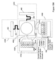
- FIG. 1 is a schematic, partially exploded, perspective view of a prior art digital camera
- FIG. 2A is a schematic cross sectional view showing the operation of the lens assembly of the prior art camera of FIG. 1 , in a retracted mode;
- FIG. 2B is a schematic cross sectional view showing the operation of the lens assembly of the prior art camera of FIG. 1 , in an optical zoom mode;
- FIG. 3 is a schematic, partially exploded, perspective view of one embodiment of a digital camera, in accordance with certain aspects of the invention.
- FIG. 4 shows one embodiment of a digital camera apparatus employed in the digital camera of FIG. 3 , partially in schematic, partially exploded, perspective view, and partially in block diagram representation, in accordance with certain aspects of the present invention
- FIGS. 5A-5V are schematic block diagram representations of various embodiments of optics portions that may be employed in the digital camera apparatus of FIG. 4 , in accordance with certain aspects of the present invention
- FIG. 5W shows another embodiment of an optics portion that may be employed in the digital camera apparatus of FIG. 4 , partially in schematic, partially exploded, perspective view and partially in schematic representation, in accordance with certain aspects of the present invention
- FIG. 5X is a schematic, exploded perspective view of one embodiment of an optics portion that may be employed in the digital camera apparatus of FIG. 4 ;
- FIG. 6A is a schematic representation of one embodiment of a sensor portion that may be employed in the digital camera apparatus of FIG. 4 , in accordance with certain aspects of the present invention
- FIG. 6B is a schematic representation of one embodiment of a sensor portion and circuits that may be connected thereto, which may be employed in the digital camera apparatus of FIG. 4 , in accordance with certain aspects of the present invention
- FIG. 7A is an enlarged view of a portion of the sensor portion of FIGS. 6A-6B and a representation of an image of an object striking the portion of the sensor portion;
- FIG. 7B is a representation of a portion of the image of FIG. 7A captured by the portion of the sensor portion of FIG. 7A ;
- FIG. 8A is an enlarged view of a portion of another embodiment of the sensor portion and a representation of an image of an object striking the portion of the sensor portion;
- FIG. 8B is a representation of a portion of the image of FIG. 8A captured by the portion of the sensor portion of FIG. 8A ;
- FIG. 9A is a block diagram representation of an optics portion and a sensor portion that may be employed in the digital camera apparatus of FIG. 4 , prior to relative movement between the optics portion and the sensor portion therebetween, in accordance with one embodiment of the present invention
- FIGS. 9B-9I are block diagram representations of the optics portion and the sensor portion of FIG. 9A after various types of relative movement therebetween, in accordance with certain aspects of the present invention.
- FIG. 9J is a schematic representation of an optics portion and a sensor portion that may be employed in the digital camera apparatus of FIG. 4 , prior to relative movement between the optics portion and the sensor portion, in accordance with one embodiment of the present invention
- FIGS. 9K-9T are block diagram representations of the optics portion and the sensor portion of FIG. 9J after various types of relative movement therebetween, and dotted lines representing the position of the optics portion prior to relative movement between the optics portion and the sensor portion, in accordance with certain aspects of the present invention
- FIG. 10A is schematic representation of an optics portion and a sensor portion that may be employed in the digital camera apparatus of FIG. 4 , prior to relative movement between the optics portion and the sensor portion, in accordance with another embodiment of the present invention
- FIGS. 10B-10Y are block diagram representations of the optics portion and the sensor portion of FIG. 10A after various types of relative movement therebetween, in accordance with certain aspects of the present invention.
- FIG. 11A is schematic representation of an optics portion and a sensor portion that may be employed in the digital camera apparatus of FIG. 4 , prior to relative movement between the optics portion and the sensor portion, in accordance with another embodiment of the present invention
- FIGS. 11B-11E are block diagram representations of the optics portion and the sensor portion of FIG. 11A after various types of relative movement therebetween, in accordance with certain aspects of the present invention.
- FIGS. 12A-12Q are block diagram representations showings example configurations of optics portions and positioning systems that may be employed in the digital camera apparatus of FIG. 4 , in accordance with various embodiments of the present invention
- FIGS. 12R-12S are block diagram representations showings example configurations of optics portions, sensor portions and one or more actuators that may be employed in the digital camera apparatus of FIG. 4 , in accordance with various embodiments of the present invention
- FIGS. 12 T- 12 AA are block diagram representations showings example configurations of optics portions, sensor portions, a processor and one or more actuators that may be employed in the digital camera apparatus of FIG. 4 , in accordance with various embodiments of the present invention
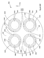
- FIGS. 13A-13D are block diagram representations of portions of various embodiments of a digital camera apparatus that includes four optics portions and a positioning system, in accordance with various embodiments of the present invention
- FIG. 13E is a block diagram representation of a portion of a digital camera apparatus that includes four optics portions and four sensor portions, with the four optics portions and the four sensor portions in a first relative positioning, in accordance with one embodiment of the present invention
- FIGS. 13F-13O are block diagram representations of the portion of the digital camera apparatus of FIG. 13E , with the four optics portions and the four sensor portions in various states of relative positioning, after various types of movement of one or more of the four optics portions, in accordance with various embodiments of the present invention
- FIGS. 14A-14D are block diagram representations of portions of various embodiments of a digital camera apparatus that includes four sensor portions and a positioning system, in accordance with various embodiments of the present invention.
- FIG. 15A shows one embodiment of the digital camera apparatus of FIG. 4 , partially in schematic, partially exploded, perspective view and partially in block diagram representation;
- FIGS. 15B-15C are an enlarged schematic plan view and an enlarged schematic representation, respectively, of one embodiment of optics portions and a positioner employed in the digital camera apparatus of FIG. 15A ;
- FIGS. 15D-15E are an enlarged schematic plan view and an enlarged schematic representation of a portion of the positioner of FIGS. 15A-15C ;
- FIG. 15F is an enlarged schematic plan view of an optics portion and a portion of the positioner of the digital camera apparatus of FIGS. 15A-15E , with the portion of the positioner shown in a first state;
- FIGS. 15G-15I are enlarged schematic plan views of the optics portion and the portion of the positioner of FIG. 15F , with the portion of the positioner in various states;
- FIG. 15J shows one embodiment, partially in schematic plan view and partially in block diagram, of a portion of a positioner and a portion of a controller that may be employed in the digital camera apparatus illustrated in FIGS. 15A-15I ;
- FIG. 15K shows another embodiment, partially in schematic plan view and partially in block diagram, of a portion of a positioner and a portion of a controller that may be employed in the digital camera apparatus illustrated in FIGS. 15A-15I ;
- FIG. 15L shows another embodiment, partially in schematic plan view and partially in block diagram, of a portion of a positioner and a portion of a controller that may be employed in the digital camera apparatus illustrated in FIGS. 15A-15I ;
- FIG. 15M shows the portion of the positioner and the portion of the controller illustrated in FIG. 15J , without two of the actuators and a portion of the controller, in conjunction with a schematic representation of one embodiment of springs and spring anchors that may be employed in association with one or more actuators of the positioner;
- FIGS. 16A-16E are enlarged schematic representations of another embodiment of optics portions and a positioner that may be employed in the digital camera apparatus of FIG. 4 , with the positioner in various states to provide various positioning of the optics portions;
- FIG. 17A shows another embodiment of the digital camera apparatus of FIG. 4 , partially in schematic, partially exploded, perspective view and partially in block diagram representation;
- FIGS. 17B-17C are an enlarged schematic plan view and an enlarged schematic representation, respectively, of one embodiment of optics portions and a positioner employed in the digital camera apparatus of FIG. 17A ;
- FIGS. 17D-17E are an enlarged schematic plan view and an enlarged schematic representation of a portion of the positioner of FIGS. 17A-17C ;
- FIG. 17F is an enlarged schematic plan view of an optics portion and a portion of the positioner of the digital camera apparatus of FIGS. 17A-17E , with the portion of the positioner shown in a first state;
- FIGS. 17G-17I are enlarged schematic plan views of the optics portion and the portion of the positioner of FIG. 17F , with the portion of the positioner in various states;
- FIGS. 18A-18E are enlarged schematic representations of one embodiment of optics portions and a positioner that may be employed in the digital camera apparatus of FIG. 4 , with the positioner in various states to provide various positioning of the optics portions;
- FIG. 19A shows another embodiment, partially in schematic plan view and partially in block diagram, of a portion of a positioner and a portion of a controller that may be employed in the digital camera apparatus illustrated in FIGS. 17A-17I ;
- FIG. 19B shows another embodiment, partially in schematic plan view and partially in block diagram, of a portion of a positioner and a portion of a controller that may be employed in the digital camera apparatus illustrated in FIGS. 17A-17I ;
- FIG. 19C shows another embodiment, partially in schematic plan view and partially in block diagram, of a portion of a positioner and a portion of a controller that may be employed in the digital camera apparatus illustrated in FIGS. 17A-17I ;
- FIG. 19D shows another embodiment, partially in schematic plan view and partially in block diagram, of a portion of a positioner and a portion of a controller that may be employed in the digital camera apparatus illustrated in FIGS. 17A-17I ;
- FIG. 19E shows another embodiment, partially in schematic plan view and partially in block diagram, of a portion of a positioner and a portion of a controller that may be employed in the digital camera apparatus illustrated in FIGS. 17A-17I ;
- FIG. 19F shows another embodiment, partially in schematic plan view and partially in block diagram, of a portion of a positioner and a portion of a controller that may be employed in the digital camera apparatus illustrated in FIGS. 17A-17I ;
- FIG. 19G shows another embodiment, partially in schematic plan view and partially in block diagram, of a portion of a positioner and a portion of a controller that may be employed in the digital camera apparatus illustrated in FIGS. 17A-17I ;
- FIG. 19H shows another embodiment, partially in schematic plan view and partially in block diagram, of a portion of a positioner and a portion of a controller that may be employed in the digital camera apparatus illustrated in FIGS. 17A-17I ;
- FIG. 19I shows another embodiment, partially in schematic plan view and partially in block diagram, of a portion of a positioner and a portion of a controller that may be employed in the digital camera apparatus illustrated in FIGS. 17A-17I ;
- FIG. 19J shows another embodiment, partially in schematic plan view and partially in block diagram, of a portion of a positioner and a portion of a controller that may be employed in the digital camera apparatus illustrated in FIGS. 17A-17I ;
- FIG. 20A shows another embodiment, partially in schematic plan view and partially in block diagram, of a portion of a positioner and a portion of a controller that may be employed in the digital camera apparatus illustrated in FIGS. 17A-17I , in accordance with another aspect of the present invention
- FIG. 20B shows another embodiment, partially in schematic plan view and partially in block diagram, of a portion of a positioner and a portion of a controller that may be employed in the digital camera apparatus illustrated in FIGS. 17A-17I , in accordance with another aspect of the present invention
- FIG. 20C shows another embodiment, partially in schematic plan view and partially in block diagram, of a portion of a positioner and a portion of a controller that may be employed in the digital camera apparatus illustrated in FIGS. 17A-17I , in accordance with another aspect of the present invention
- FIG. 20D shows another embodiment, partially in schematic plan view and partially in block diagram, of a portion of a positioner and a portion of a controller that may be employed in the digital camera apparatus illustrated in FIGS. 17A-17I , in accordance with another aspect of the present invention
- FIGS. 21A-21B are an enlarged schematic plan view and an enlarged schematic representation, respectively, of another embodiment of optics portions and a positioner that may be employed in the digital camera apparatus of FIG. 4 , in accordance with another aspect of the present invention
- FIGS. 21C-21D are an enlarged schematic plan view and an enlarged schematic representation, respectively, of another embodiment of optics portions and a positioner that may be employed in the digital camera apparatus of FIG. 4 , in accordance with another aspect of the present invention.
- FIG. 22 is an enlarged schematic representation, respectively, of another embodiment of optics portions and a positioner that may be employed in the digital camera apparatus of FIG. 4 , in accordance with another aspect of the present invention
- FIG. 23A-23D are enlarged schematic representations of another embodiment of optics portions and a positioner that may be employed in the digital camera apparatus of FIG. 4 , with the positioner in various states to provide various positioning of the optics portions, in accordance with another aspect of the present invention
- FIG. 24A-24D are enlarged schematic representations of another embodiment of optics portions and a positioner that may be employed in the digital camera apparatus of FIG. 4 , with the positioner in various states to provide various positioning of the optics portions, in accordance with another aspect of the present invention
- FIG. 25A-25D are enlarged schematic representations of another embodiment of optics portions and a positioner that may be employed in the digital camera apparatus of FIG. 4 , with the positioner in various states to provide various positioning of the optics portions, in accordance with another aspect of the present invention;
- FIG. 26A-26D are enlarged schematic representations of another embodiment of optics portions and a positioner that may be employed in the digital camera apparatus of FIG. 4 , with the positioner in various states to provide various positioning of the optics portions, in accordance with another aspect of the present invention;
- FIG. 27A-27D are enlarged schematic representations of another embodiment of optics portions and a positioner that may be employed in the digital camera apparatus of FIG. 4 , with the positioner in various states to provide various positioning of the optics portions, in accordance with another aspect of the present invention;
- FIG. 28A is an enlarged schematic representation of another embodiment of optics portions and a positioner that may be employed in the digital camera apparatus of FIG. 4 , with the positioner shown in a first state to provide a first positioning of the optics portions, in accordance with another aspect of the present invention
- FIG. 28B is an enlarged schematic representation of another embodiment of optics portions and a positioner that may be employed in the digital camera apparatus of FIG. 4 , with the positioner shown in a first state to provide a first positioning of the optics portions, in accordance with another aspect of the present invention
- FIG. 28C is an enlarged schematic representation of another embodiment of optics portions and a positioner that may be employed in the digital camera apparatus of FIG. 4 , with the positioner shown in a first state to provide a first positioning of the optics portions, in accordance with another aspect of the present invention
- FIG. 28D is an enlarged schematic representation of another embodiment of optics portions and a positioner that may be employed in the digital camera apparatus of FIG. 4 , with the positioner shown in a first state to provide a first positioning of the optics portions, in accordance with another aspect of the present invention
- FIG. 29 is an enlarged schematic representation of another embodiment of optics portions and a positioner that may be employed in the digital camera apparatus of FIG. 4 , with the positioner shown in a first state to provide a first positioning of the optics portions, in accordance with another aspect of the present invention
- FIG. 30 is an enlarged schematic representation of another embodiment of optics portions and a positioner that may be employed in the digital camera apparatus of FIG. 4 , with the positioner shown in a first state to provide a first positioning of the optics portions, in accordance with another aspect of the present invention
- FIGS. 31A-31B are an enlarged schematic plan view and an enlarged schematic representation, respectively, of optics portions and a positioner that may be employed in the digital camera apparatus of FIG. 4 , with the positioner shown in a first state to provide a first positioning of the optics portions, in accordance with another aspect of the present invention;
- FIGS. 31C-31D are an enlarged schematic plan view and an enlarged schematic representation, respectively, of optics portions and a positioner that may be employed in the digital camera apparatus of FIG. 4 , with the positioner shown in a first state to provide a first positioning of the optics portions, in accordance with another aspect of the present invention;
- FIGS. 31E-31F are an enlarged schematic plan view and an enlarged schematic representation, respectively, of optics portions and a positioner that may be employed in the digital camera apparatus of FIG. 4 , with the positioner shown in a first state to provide a first positioning of the optics portions, in accordance with another aspect of the present invention;
- FIGS. 31G-31H are an enlarged schematic plan view and an enlarged schematic representation, respectively, of optics portions and a positioner that may be employed in the digital camera apparatus of FIG. 4 , with the positioner shown in a first state to provide a first positioning of the optics portions, in accordance with another aspect of the present invention;
- FIGS. 31I-31J are an enlarged schematic plan view and an enlarged schematic representation, respectively, of optics portions and a positioner that may be employed in the digital camera apparatus of FIG. 4 , with the positioner shown in a first state to provide a first positioning of the optics portions, in accordance with another aspect of the present invention;
- FIGS. 31K-31L are an enlarged schematic plan view and an enlarged schematic representation, respectively, of optics portions and a positioner that may be employed in the digital camera apparatus of FIG. 4 , with the positioner shown in a first state to provide a first positioning of the optics portions, in accordance with another aspect of the present invention;
- FIGS. 31M-31N are an enlarged schematic plan view and an enlarged schematic representation, respectively, of an optics portion and a positioner that may be employed in the digital camera apparatus of FIG. 4 , with the positioner shown in a first state to provide a first positioning of the optics portions, in accordance with another aspect of the present invention;
- FIGS. 31O-31P are an enlarged schematic plan view and an enlarged schematic representation, respectively, of optics portions and a positioner that may be employed in the digital camera apparatus of FIG. 4 , with the positioner shown in a first state to provide a first positioning of the optics portions, in accordance with another aspect of the present invention;
- FIGS. 31Q-31R are an enlarged schematic plan view and an enlarged schematic representation, respectively, of optics portions and a positioner that may be employed in the digital camera apparatus of FIG. 4 , with the positioner shown in a first state to provide a first positioning of the optics portions, in accordance with another aspect of the present invention;
- FIGS. 31S-31T are an enlarged schematic plan view and an enlarged schematic representation, respectively, of optics portions and a positioner that may be employed in the digital camera apparatus of FIG. 4 , with the positioner shown in a first state to provide a first positioning of the optics portions, in accordance with another aspect of the present invention;
- FIGS. 32A-32B are an enlarged schematic plan view and an enlarged schematic representation, respectively, of optics portions and a positioner that may be employed in the digital camera apparatus of FIG. 4 , with the positioner shown in a first state to provide a first positioning of the optics portions, in accordance with another aspect of the present invention;
- FIGS. 32C-32D are an enlarged schematic plan view and an enlarged schematic representation, respectively, of optics portions and a positioner that may be employed in the digital camera apparatus of FIG. 4 , with the positioner shown in a first state to provide a first positioning of the optics portions, in accordance with another aspect of the present invention;
- FIGS. 32E-32F are an enlarged schematic plan view and an enlarged schematic representation, respectively, of optics portions and a positioner that may be employed in the digital camera apparatus of FIG. 4 , with the positioner shown in a first state to provide a first positioning of the optics portions, in accordance with another aspect of the present invention;
- FIGS. 32G-32H are an enlarged schematic plan view and an enlarged schematic representation, respectively, of optics portions and a positioner that may be employed in the digital camera apparatus of FIG. 4 , with the positioner shown in a first state to provide a first positioning of the optics portions, in accordance with another aspect of the present invention;
- FIGS. 32I-32J are an enlarged schematic plan view and an enlarged schematic representation, respectively, of optics portions and a positioner that may be employed in the digital camera apparatus of FIG. 4 , with the positioner shown in a first state to provide a first positioning of the optics portions, in accordance with another aspect of the present invention;
- FIGS. 32K-32L are an enlarged schematic plan view and an enlarged schematic representation, respectively, of optics portions and a positioner that may be employed in the digital camera apparatus of FIG. 4 , with the positioner shown in a first state to provide a first positioning of the optics portions, in accordance with another aspect of the present invention;
- FIGS. 32M-32N are an enlarged schematic plan view and an enlarged schematic representation, respectively, of optics portions and a positioner that may be employed in the digital camera apparatus of FIG. 4 , with the positioner shown in a first state to provide a first positioning of the optics portions, in accordance with another aspect of the present invention;
- FIGS. 32O-32P are an enlarged schematic plan view and an enlarged schematic representation, respectively, of optics portions and a positioner that may be employed in the digital camera apparatus of FIG. 4 , with the positioner shown in a first state to provide a first positioning of the optics portions, in accordance with another aspect of the present invention;
- FIGS. 33A-33B are an enlarged schematic plan view and an enlarged schematic representation, respectively, of portions of optics portions and a positioner that may be employed in the digital camera apparatus of FIG. 4 , with the positioner shown in a first state to provide a first positioning of the portions of optics portions, in accordance with another aspect of the present invention;
- FIGS. 33C-33D are an enlarged schematic plan view and an enlarged schematic representation, respectively, of portions of optics portions and a positioner that may be employed in the digital camera apparatus of FIG. 4 , with the positioner shown in a first state to provide a first positioning of the portions of optics portions, in accordance with another aspect of the present invention;
- FIGS. 33E-33F are an enlarged schematic plan view and an enlarged schematic representation, respectively, of portions of optics portions and a positioner that may be employed in the digital camera apparatus of FIG. 4 , with the positioner shown in a first state to provide a first positioning of the portions of optics portions, in accordance with another aspect of the present invention;
- FIGS. 33G-33H are an enlarged schematic plan view and an enlarged schematic representation, respectively, of portions of optics portions and a positioner that may be employed in the digital camera apparatus of FIG. 4 , with the positioner shown in a first state to provide a first positioning of the portions of optics portions, in accordance with another aspect of the present invention;
- FIGS. 33I-33J are an enlarged schematic plan view and an enlarged schematic representation, respectively, of sensor portions and a positioner that may be employed in the digital camera apparatus of FIG. 4 , with the positioner shown in a first state to provide a first positioning of the sensor portions, in accordance with another aspect of the present invention;
- FIGS. 33K-33L are a schematic plan view and a schematic representation, respectively, of optics portions and a positioner that may be employed in the digital camera apparatus of FIG. 4 , with the positioner shown in a first state to provide a first positioning of the sensor portions, in accordance with another aspect of the present invention;
- FIGS. 33M-33N are a schematic plan view and a schematic representation, respectively, of sensor portions and a positioner that may be employed in the digital camera apparatus of FIG. 4 , with the positioner shown in a first state to provide a first positioning of the sensor portions, in accordance with another aspect of the present invention;
- FIGS. 34A-34B are an enlarged schematic plan view and an enlarged schematic representation, respectively, of portions of optics portions and a positioner that may be employed in the digital camera apparatus of FIG. 4 , with the positioner shown in a first state to provide a first positioning of the portions of optics portions, in accordance with another aspect of the present invention;
- FIGS. 34C-34D are an enlarged schematic plan view and an enlarged schematic representation, respectively, of portions of optics portions and a positioner that may be employed in the digital camera apparatus of FIG. 4 , with the positioner shown in a first state to provide a first positioning of the portions of optics portions, in accordance with another aspect of the present invention;
- FIGS. 34E-34F are an enlarged schematic plan view and an enlarged schematic representation, respectively, of portions of optics portions and a positioner that may be employed in the digital camera apparatus of FIG. 4 , with the positioner shown in a first state to provide a first positioning of the portions of optics portions, in accordance with another aspect of the present invention;
- FIGS. 34G-34H are an enlarged schematic plan view and an enlarged schematic representation, respectively, of portions of optics portions and a positioner that may be employed in the digital camera apparatus of FIG. 4 , with the positioner shown in a first state to provide a first positioning of the portions of optics portions, in accordance with another aspect of the present invention;
- FIGS. 34I-34J are an enlarged schematic plan view and an enlarged schematic representation, respectively, of sensor portions and a positioner that may be employed in the digital camera apparatus of FIG. 4 , with the positioner shown in a first state to provide a first positioning of the sensor portions, in accordance with another aspect of the present invention;
- FIGS. 34K-34L are a schematic plan view and a schematic representation, respectively, of optics portions and a positioner that may be employed in the digital camera apparatus of FIG. 4 , with the positioner shown in a first state to provide a first positioning of the sensor portions, in accordance with another aspect of the present invention;
- FIGS. 34M-34N are a schematic plan view and a schematic representation, respectively, of sensor portions and a positioner that may be employed in the digital camera apparatus of FIG. 4 , with the positioner shown in a first state to provide a first positioning of the sensor portions, in accordance with another aspect of the present invention;
- FIG. 35A is a block diagram of one embodiment of a controller that may be employed in the digital camera apparatus of FIG. 4 ;
- FIG. 35B is a table representing one embodiment of a mapping that may be employed by a position scheduler of the controller of FIG. 35A ;
- FIG. 35C is a schematic diagram of one embodiment of a driver bank that may be employed by the controller of FIG. 35A ;
- FIG. 35D is a block diagram of another embodiment of a driver bank that may be employed by the controller of FIG. 35A ;
- FIG. 35E is a flowchart of steps employed in one embodiment in generating a mapping for the position scheduler of FIG. 35A and/or to calibrate the positioning system of the digital camera apparatus of FIG. 4 ;
- FIGS. 35F-35H is a flowchart of steps employed in one embodiment in generating a mapping for the position scheduler of FIG. 35A and/or to calibrate the positioning system of the digital camera apparatus of FIG. 4 ;
- FIGS. 35I-35J is a schematic of signals employed in one embodiment of the controller of FIG. 35A ;
- FIG. 36A is a block diagram of sensor portions and an image processor that may be employed in the digital camera apparatus of FIG. 4 , in accordance with one embodiment of aspects of the present invention
- FIG. 36B is a block diagram of one embodiment of a channel processor that may be employed in the image processor of FIG. 36A , in accordance with one embodiment of the present invention
- FIG. 36C is a block diagram of an one embodiment of an image pipeline that may be employed in the image processor of FIG. 36A ;
- FIG. 36D is a block diagram of one embodiment of an image post processor that may be employed in the image processor of FIG. 36A ;
- FIG. 36E is a block diagram of one embodiment of a system control portion that may be employed in the image processor of FIG. 36A ;
- FIG. 37A is a block diagram of another embodiment of a channel processor that may be employed in the image processor of FIG. 36A ;
- FIG. 37B is a graphical representation of a neighborhood of pixel values and a plurality of spatial directions
- FIG. 37C is a flowchart of steps that may be employed in one embodiment of a double sampler, which may be employed in the channel processor of FIG. 37A ;
- FIG. 37D shows a flowchart of steps employed in one embodiment of a defective pixel identifier, which may be employed in the channel processor of FIG. 37A ;
- FIG. 37E is a block diagram of another embodiment of an image pipeline that may be employed in the image processor of FIG. 36A ;
- FIG. 37F is a block diagram of one embodiment of an image plane integrator that may be employed in the image pipeline of FIG. 37E ;
- FIG. 37G is a graphical representation of a multi-phase clock that may be employed in the image plane integrator of FIG. 37F ;
- FIG. 37H is a block diagram of one embodiment of automatic exposure control that may be employed in the image pipeline of FIG. 37E ;
- FIG. 37I is a graphical representation showing an example of operation of a gamma correction stage that may be employed in the image pipeline of FIG. 37E ;
- FIG. 37J is a block diagram of one embodiment of a gamma correction stage that may be employed in the image pipeline of FIG. 37E ;
- FIG. 37K is a block diagram of one embodiment of a color correction stage that may be employed in the image pipeline of FIG. 37E ;
- FIG. 37L is a block diagram of one embodiment of a high pass filter stage that may be employed in the image pipeline of FIG. 37E ;
- FIG. 38 is a block diagram of another embodiment of a channel processor that may be employed in the image processor of FIG. 36A ;
- FIG. 39 is a block diagram of another embodiment of a channel processor that may be employed in the image processor of FIG. 36A ;
- FIG. 40 is a block diagram of another embodiment of an image pipeline that may be employed in the image processor of FIG. 36A ;
- FIG. 41A is an enlarged view of a portion of a sensor, for example, the sensor of FIG. 6A , and a representation of an image of an object striking the portion of the sensor, with the sensor and associated optics in a first relative positioning;
- FIG. 41B is a representation of a portion of the image of FIG. 41A captured by the portion of the sensor of FIG. 41A , with the sensor and the optics in the first relative positioning;
- FIG. 41C is an enlarged view of the portion of the sensor of FIG. 41A and a representation of the image of the object striking the portion of the sensor, with the sensor and the associated optics in a second relative positioning;
- FIG. 41D is a representation of a portion of the image of FIG. 41C captured by the portion of the sensor of FIG. 41C , with the sensor and the optics in the second relative positioning;
- FIG. 41E is an explanatory view showing a relationship between the first relative positioning and the second relative positioning, wherein dotted circles indicate the position of sensor elements relative to the image of the object with the sensor and the optics in the first relative positioning, and solid circles indicate the position of the sensor elements relative to the image of the object with the sensor and optics in the second relative positioning;
- FIG. 41F is a representation showing a combination of the portion of the image captured with the first relative positioning, as represented in FIG. 41B , and the portion of the image captured with the second relative positioning, as represented in FIG. 41D ;
- FIG. 41G is an enlarged view of the portion of the sensor of FIG. 41A and a representation of the image of the object striking the portion of the sensor, with the sensor and the associated optics in a third relative positioning;
- FIG. 41H is a representation of a portion of the image of FIG. 41G captured by the portion of the sensor of FIG. 41G , with the sensor and the optics in the third relative positioning;
- FIG. 41I is an explanatory view showing a relationship between the first relative positioning, the second relative positioning and the third relative positioning, wherein a first set of dotted circles indicate the position of the sensor elements relative to the image of the object with the sensor and the optics in the first relative positioning, a second set of dotted circles indicate the position of the sensor elements relative to the image of the object with the sensor and the optics in the second relative positioning, and solid circles indicate the position of the sensor elements relative to the image of the object with the sensor and the optics in the third relative positioning;
- FIG. 41J is a representation showing a combination of the portion of the image captured with the first relative positioning, as represented in FIG. 41B , the portion of the image captured with the second relative positioning, as represented in FIG. 41D , and the portion of the image captured with the third relative positioning, as represented in FIG. 41H ;
- FIG. 42A shows a flowchart of steps that may be employed in increasing resolution, in accordance with one embodiment of the present invention.
- FIGS. 42B-42E are diagrammatic representations of pixel values corresponding to four images
- FIG. 42F is a diagrammatic representation of pixel values corresponding to one embodiment of an image that is a combination of the four images represented in FIGS. 42B-42E ;
- FIG. 42G is a block diagram of one embodiment of an image combiner
- FIG. 42H is a block diagram of one embodiment of the image combiner of FIG. 42G ;
- FIG. 42I is a graphical representation of a multi-phase clock that may be employed in the image combiner of FIG. 42H ;
- FIG. 43 is a flowchart of steps that may be employed in increasing resolution, in accordance with another embodiment of the present invention.
- FIG. 44A is an enlarged view of a portion of a sensor, for example, the sensor of FIG. 8A , and a representation of an image of an object striking the portion of the sensor;
- FIG. 44B is a representation of a portion of the image of FIG. 44A captured by the portion of the sensor of FIG. 44A ;
- FIG. 44C is a view of the portion of the sensor of FIG. 44A and a representation of the image of FIG. 44A , and a window identifying a portion to be enlarged;
- FIG. 44D is an enlarged view of a portion of the sensor of FIG. 44C within the window of FIG. 44C and an enlarged representation of a portion of the image of FIG. 44C within the window of FIG. 44C ;
- FIG. 44E is a representation of an image produced by enlarging the portion of the image of FIG. 44C within the window of FIG. 44C ;
- FIG. 44F is a view of the portion of the sensor of FIG. 44A and a representation of an image of an object striking the portion of the sensor after optical zooming;
- FIG. 44G is a representation of an image produced by optical zooming
- FIG. 45A is an enlarged view of a portion of a sensor, for example, the sensor of FIG. 8A , a representation of an image of an object striking the portion of the sensor, and a window identifying a portion to be enlarged;
- FIG. 45B is a representation of a portion of the image of FIG. 45A captured by the portion of the sensor of FIG. 45A ;
- FIG. 45C is an enlarged view of a portion of the sensor of FIG. 45A within the window of FIG. 45A and an enlarged representation of a portion of the image of FIG. 45A within the window of FIG. 45A ;
- FIG. 45D is an representation of a portion of the image of FIG. 45C captured by the portion of the sensor of FIG. 45C ;
- FIG. 45E is an enlarged view of the portion of the sensor of FIG. 45C and a representation of the image of the object striking the portion of the sensor, with the sensor and the associated optics in a second relative positioning;
- FIG. 45F is a representation of a portion of the image captured by the portion of the sensor of FIG. 45E , with the sensor and the optics in the second relative positioning;
- FIG. 45G is an explanatory view showing a relationship between the first relative positioning and the second relative positioning, wherein dotted circles indicate the position of sensor elements relative to the image of the object with the sensor and the optics in the first relative positioning and solid circles indicate the position of the sensor elements relative to the image of the object with the sensor and the optics in the second relative positioning;
- FIG. 45H is a representation showing a combination of the portion of the image captured with the first relative positioning, as represented in FIG. 45D and the portion of the image captured with the second relative positioning, as represented in FIG. 45F ;
- FIG. 45I is an enlarged view of the portion of the sensor of FIG. 45C and a representation of the image of the object striking the portion of the sensor, with the sensor and the associated optics in a third relative positioning;
- FIG. 45J is a representation of a portion of the image captured by the portion of the sensor of FIG. 45I , with the sensor and the optics in the third relative positioning;
- FIG. 45K is an explanatory view showing a relationship between the first relative positioning, the second relative positioning and the third relative positioning, wherein a first set of dotted circles indicate the position of sensor elements relative to the image of the object with the sensor and the optics in the first relative positioning, a second set of dotted circles indicate the position of sensor elements relative to the image of the object with the sensor and the optics in the second relative positioning, and solid circles indicate the position of the sensor elements relative to the image of the object with the sensor and the optics in the third relative positioning;
- FIG. 45L is a representation showing a combination of the portion of the image captured with the first relative positioning, as represented in FIG. 45D , the portion of the image captured with the second relative positioning, as represented in FIG. 45F , and the portion of the image captured with the second relative positioning, as represented in FIG. 45J ;
- FIG. 46A is a flowchart of steps that may be employed in providing zoom, according to one embodiment of the present invention.
- FIG. 46B is a block diagram of one embodiment that may be employed in generating a zoom image
- FIG. 47A is a flowchart of steps that may be employed in providing zoom, according to another embodiment of the present invention.
- FIG. 47B is a flowchart of steps that may be employed in providing zoom, according to another embodiment of the present invention.
- FIGS. 48A-48G show steps used in providing image stabilization according to one embodiment of aspects of the present invention.
- FIGS. 49A-49B are a flowchart of the steps used in providing image stabilization in one embodiment of aspects of the present invention.
- FIGS. 50A-50N show examples of misalignment of one or more camera channels in the digital camera apparatus of FIG. 4 and one or more movements that could be used to compensate for such;
- FIG. 51A is a flowchart of steps that may be employed in providing alignment, according to one embodiment of the present invention.
- FIG. 51B is a flowchart of steps that may be employed in providing alignment; according to another embodiment of the present invention.
- FIG. 52A is a flowchart of steps that may be employed in providing alignment, according to another embodiment of the present invention.
- FIG. 52B is a flowchart of steps that may be employed in providing alignment, according to another embodiment of the present invention.
- FIG. 52C is a flowchart of steps that may be employed in providing alignment; according to one embodiment of the present invention.
- FIG. 53A is a schematic perspective view of a portion of a digital camera apparatus that includes an optics portion having a mask in accordance with one embodiment of aspects of the present invention, with the mask, a lens and a sensor portion being shown in a first relative positioning;
- FIG. 53B is a schematic perspective view of the portion of the digital camera apparatus of FIG. 53A , with the mask, the lens and the sensor portion being shown in a second relative positioning;
- FIG. 53C is a schematic perspective view of the portion of the digital camera apparatus of FIG. 53A , with the mask, the lens and the sensor portion being shown in a third relative positioning;
- FIG. 53D is a schematic perspective view of a portion of a digital camera apparatus that includes an optics portion having a mask in accordance with another embodiment of aspects of the present invention, with the mask, a lens and a sensor portion being shown in a first relative positioning;
- FIG. 53E is a schematic perspective view of the portion of the digital camera apparatus of FIG. 53D , with the mask, the lens and the sensor portion being shown in a second relative positioning;
- FIG. 53F is a schematic perspective view of the portion of the digital camera apparatus of FIG. 53C , with the mask, the lens and the sensor portion being shown in a third relative positioning;
- FIG. 53G is a schematic perspective view of a portion of a digital camera apparatus that includes an optics portion having a mask in accordance with another embodiment of aspects of the present invention, with the mask, a lens and a sensor portion being shown in a first relative positioning;
- FIG. 53H is a schematic perspective view of the portion of the digital camera apparatus of FIG. 53G , with the mask, the lens and the sensor portion being shown in a second relative positioning;
- FIG. 53I is a schematic perspective view of the portion of the digital camera apparatus of FIG. 53G , with the mask, the lens and the sensor portion being shown in a third relative positioning;
- FIG. 54 is a flowchart of steps that may be employed in association with one or more masks in providing one or more masking effects, according to one embodiment of the present invention.
- FIG. 55A is a schematic perspective view of a portion of a digital camera apparatus that includes an optics portion having a mechanical shutter in accordance with one embodiment of aspects of the present invention, with the mechanical shutter, a lens and a sensor portion being shown in a first relative positioning;
- FIG. 55B is a schematic perspective view of the portion of the digital camera apparatus of FIG. 55A , with the mechanical shutter, the lens and the sensor portion being shown in a second relative positioning;
- FIG. 55C is a schematic perspective view of the portion of the digital camera apparatus of FIG. 55A , with the mechanical shutter, the lens and the sensor portion being shown in a third relative positioning;
- FIG. 55D is a schematic perspective view of a portion of a digital camera apparatus that includes an optics portion having a mechanical shutter in accordance with another embodiment of aspects of the present invention, with the mechanical shutter, a lens and a sensor portion being shown in a first relative positioning;
- FIG. 55E is a schematic perspective view of the portion of the digital camera apparatus of FIG. 55D , with the mechanical shutter, the lens and the sensor portion being shown in a second relative positioning;
- FIG. 55F is a schematic perspective view of the portion of the digital camera apparatus of FIG. 55D , with the mechanical shutter, the lens and the sensor portion being shown in a third relative positioning;
- FIG. 56 is a flowchart of steps that may be employed in association with a mechanical shutter, according to one embodiment of the present invention.
- FIGS. 57A-57B are a flowchart of steps that may be employed in association with a mechanical shutter, according to another embodiment of the present invention.
- FIG. 58A is a schematic perspective view of a portion of a digital camera apparatus that includes an optics portion having a mechanical iris in accordance with one embodiment of aspects of the present invention, with the mechanical iris, a lens and a sensor portion being shown in a first relative positioning;
- FIG. 58B is a schematic perspective view of the portion of the digital camera apparatus of FIG. 58A , with the mechanical iris, the lens and the sensor portion being shown in a second relative positioning;
- FIG. 58C is a schematic perspective view of the portion of the digital camera apparatus of FIG. 58A , with the mechanical iris, the lens and the sensor portion being shown in a third relative positioning;
- FIG. 58D is a schematic perspective view of the portion of the digital camera apparatus of FIG. 58A , with the mechanical iris, the lens and the sensor portion being shown in a fourth relative positioning;
- FIG. 58E is a schematic perspective view of a portion of a digital camera apparatus that includes an optics portion having a mechanical iris in accordance with another embodiment of aspects of the present invention, with the mechanical iris, a lens and a sensor portion being shown in a first relative positioning;
- FIG. 58F is a schematic perspective view of the portion of the digital camera apparatus of FIG. 58E , with the mechanical iris, the lens and the sensor portion being shown in a second relative positioning;
- FIG. 58G is a schematic perspective view of the portion of the digital camera apparatus of FIG. 58E , with the mechanical iris, the lens and the sensor portion being shown in a third relative positioning;
- FIG. 58H is a schematic perspective view of the portion of the digital camera apparatus of FIG. 58E , with the mechanical iris, the lens and the sensor portion being shown in a fourth relative positioning;
- FIG. 59 is a flowchart of steps that may be employed in association with a mechanical iris, according to one embodiment of the present invention.
- FIGS. 60A-60B are a flowchart of steps that may be employed in association with a mechanical iris, according to another embodiment of the present invention.
- FIG. 61A is a schematic perspective view of a portion of a digital camera apparatus that includes an optics portion having a multispectral and/or hyperspectral filter in accordance with one embodiment of aspects of the present invention, with the hyperspectral filter, a lens and a sensor portion being shown in a first relative positioning;
- FIG. 61B is a schematic perspective view of the portion of the digital camera apparatus of FIG. 61A , with the hyperspectral filter, the lens and the sensor portion being shown in a second relative positioning;
- FIG. 61C is a schematic perspective view of the portion of the digital camera apparatus of FIG. 61A , with the hyperspectral filter, the lens and the sensor portion being shown in a third relative positioning;
- FIG. 62A is a flowchart of steps that may be employed in providing hyperspectral imaging, according to one embodiment of the present invention.
- FIG. 62B is a block diagram representation of one embodiment of a combiner for generating a hyperspectral image
- FIG. 63 is a flowchart of steps that may be employed in providing hyperspectral imaging, according to another embodiment of the present invention.
- FIGS. 64A-64F are schematic plan views of various embodiments of filters that may be employed in hyperspectral imaging
- FIG. 65A is a schematic perspective view of a portion of a digital camera apparatus that includes an optics portion having a hyperspectral filter in accordance with another embodiment of aspects of the present invention, with the hyperspectral filter, a lens and a sensor portion being shown in a first relative positioning;
- FIG. 65B is a schematic perspective view of the portion of the digital camera apparatus of FIG. 65A , with the hyperspectral filter, the lens and the sensor portion being shown in a second relative positioning;
- FIG. 65C is a schematic perspective view of the portion of the digital camera apparatus of FIG. 65A , with the hyperspectral filter, the lens and the sensor portion being shown in a third relative positioning;
- FIG. 65D is a schematic perspective view of the portion of the digital camera apparatus of FIG. 65A , with the hyperspectral filter, the lens and the sensor portion being shown in a fourth relative positioning;
- FIG. 66A is a schematic perspective view of a portion of a digital camera apparatus that includes an optics portion having a hyperspectral filter in accordance with another embodiment of aspects of the present invention, with the hyperspectral filter, a lens and a sensor portion being shown in a first relative positioning;
- FIG. 66B is a schematic perspective view of the portion of the digital camera apparatus of FIG. 66A , with the hyperspectral filter, the lens and the sensor portion being shown in a second relative positioning;
- FIG. 66C is a schematic perspective view of the portion of the digital camera apparatus of FIG. 66A , with the hyperspectral filter, the lens and the sensor portion being shown in a third relative positioning;
- FIG. 66D is a schematic perspective view of the portion of the digital camera apparatus of FIG. 66A , with the hyperspectral filter, the lens and the sensor portion being shown in a fourth relative positioning;
- FIG. 66E is a schematic perspective view of a portion of a digital camera apparatus that includes an optics portion having a hyperspectral filter in accordance with another embodiment of aspects of the present invention, with the hyperspectral filter, a lens and a sensor portion being shown in a first relative positioning;
- FIG. 66F is a schematic perspective view of the portion of the digital camera apparatus of FIG. 66E , with the hyperspectral filter, the lens and the sensor portion being shown in a second relative positioning;
- FIG. 67A is a schematic perspective view of a portion of a digital camera apparatus that includes an optics portion having a hyperspectral filter in accordance with another embodiment of aspects of the present invention, with the hyperspectral filter, a lens and a sensor portion being shown in a first relative positioning;
- FIG. 67B is a schematic perspective view of the portion of the digital camera apparatus of FIG. 67A , with the hyperspectral filter, the lens and the sensor portion being shown in a second relative positioning;
- FIG. 67C is a schematic perspective view of the portion of the digital camera apparatus of FIG. 67A , with the hyperspectral filter, the lens and the sensor portion being shown in a third relative positioning;
- FIG. 67D is a schematic perspective view of the portion of the digital camera apparatus of FIG. 67A , with the hyperspectral filter, the lens and the sensor portion being shown in a fourth relative positioning;
- FIGS. 68A-68E show an example of parallax in the x direction in the digital camera apparatus 210 ;
- FIGS. 68F-68I show an example of parallax in the y direction in the digital camera apparatus of FIG. 4 ;
- FIGS. 68J-68M show an example of parallax having an x component and a y component in the digital camera apparatus of FIG. 4 ;
- FIGS. 68N-68R show an example of an effect of using movement to help decrease parallax in the digital camera apparatus
- FIGS. 68S-68W show an example of an effect of using movement to help increase parallax in the digital camera apparatus
- FIG. 69 is a flowchart of steps that may be employed to increase and/or decrease parallax, according to one embodiment of the present invention.
- FIGS. 70-71 show a flowchart of steps that may be employed and/or decrease parallax in another embodiment of the present invention.
- FIGS. 72A-72B is a flowchart of steps that may be employed in generating an estimate of a distance to an object, or portion thereof, according to one embodiment of the present invention.
- FIG. 73 is a block diagram of a portion of one embodiment of a range finder that may be employed in generating an estimate of a distance to an object, or portion thereof;
- FIGS. 74A-74B show an example of images that may be employed in providing stereovision
- FIG. 75 shows one embodiment of eyewear that may be employed in providing stereovision
- FIG. 76 is a representation of one embodiment of an image with a 3D effect
- FIGS. 77A-77B show a flowchart of steps that may be employed in providing 3D imaging, according to one embodiment of the present invention.
- FIG. 78 is a block diagram of one embodiment for generating an image with a 3D effect
- FIG. 79 is a block diagram of one embodiment for generating an image with 3D graphics
- FIG. 80 is a flowchart of steps that may be employed in providing image discrimination, according to one embodiment of the present invention.
- FIGS. 81A-81B show a flowchart of steps that may be employed in providing image discrimination, according to another embodiment of the present invention.
- FIG. 82 shows a flowchart of steps that may be employed in providing auto focus, according to one embodiment of the present invention.
- FIG. 83A is a schematic cross sectional view (taken, for example, in a direction such as direction A-A shown on FIGS. 15A , 17 A) of one embodiment of the digital camera apparatus and a circuit board of a digital camera on which the digital camera apparatus may be mounted;
- FIG. 83B is a schematic cross sectional view (taken, for example, in a direction such as direction A-A shown on FIGS. 15A , 17 A) of another embodiment of the digital camera apparatus and a circuit board of the digital camera on which the digital camera apparatus may be mounted;
- FIG. 83C is a schematic plan view of one side of one embodiment of a positioner of the digital camera apparatus of FIG. 83A ;
- FIG. 83D is a schematic cross section view of one embodiment of optics portions, a positioner and a second integrated circuit of the digital camera apparatus of FIG. 83A .
- FIG. 83E is a plan view of a side of one embodiment of a first integrated circuit die of the digital camera apparatus of FIG. 83A ;
- FIG. 83F is a schematic cross section view of one embodiment of a first integrated circuit die of the digital camera apparatus of FIG. 83A ;
- FIG. 84A is a schematic representation of another embodiment of an optics portion and a portion of another embodiment of a positioner of the digital camera apparatus;
- FIG. 84B is a schematic representation view of another embodiment of an optics portion and a portion of another embodiment of a positioner of the digital camera apparatus;
- FIG. 84C is a schematic representation view of another embodiment of an optics portion and a portion of another embodiment of a positioner of the digital camera apparatus;
- FIG. 85A is a schematic representation of one embodiment of the digital camera apparatus that includes the optics portion and positioner of FIG. 84A ;
- FIG. 85B is a schematic representation of one embodiment of the digital camera apparatus that includes the optics portion and positioner of FIG. 84B ;
- FIG. 85C is a schematic representation of one embodiment of the digital camera apparatus that includes the optics portion and positioner of FIG. 84C ;
- FIGS. 86A-86B are an enlarged schematic representation and an enlarged schematic perspective view, respectively, of one embodiment of a digital camera apparatus having three camera channels;
- FIGS. 87A-87B are an enlarged schematic perspective view and an enlarged representation view of another embodiment of a digital camera apparatus having three camera channels;
- FIG. 87C is an enlarged schematic perspective view of a portion of the digital camera apparatus of FIGS. 87A-87B ;
- FIG. 88 is a schematic perspective representation of one embodiment of a digital camera apparatus
- FIG. 89 is a schematic perspective representation of the digital camera apparatus of FIG. 88 , in exploded view form;
- FIGS. 90A-90H show one embodiment for assembling and mounting one embodiment of the digital camera apparatus of FIG. 4 ;
- FIGS. 90I-90N show one embodiment for assembling and mounting another embodiment of a digital camera apparatus
- FIGS. 90O-90V shows one embodiment for assembling and mounting another embodiment of a digital camera apparatus
- FIG. 91 is a perspective partially exploded representation of another embodiment of a digital camera apparatus.
- FIGS. 92A-92D are schematic representations of a portion of another embodiment of a digital camera apparatus
- FIG. 93 is a schematic representation of another embodiment of a positioner and optics portions for a digital camera apparatus
- FIG. 94 a schematic representation of another embodiment of a positioner and optics portions for a digital camera apparatus
- FIG. 95A a schematic representation of another embodiment of a positioner and optics portions for a digital camera apparatus
- FIG. 95B a schematic representation of another embodiment of a positioner and optics portions for a digital camera apparatus
- FIG. 96 is a perspective partially exploded schematic representation of another embodiment a digital camera apparatus
- FIG. 97 is a partially exploded schematic representation of one embodiment of a digital camera apparatus
- FIG. 98 is a schematic representation of a camera system having two digital camera apparatus mounted back to back;
- FIG. 99 is a representation of a digital camera apparatus that includes a molded plastic packaging
- FIG. 100 is a representation of a digital camera apparatus that includes a ceramic packaging
- FIGS. 101A-101F and 102 A- 102 D are schematic representations of some other configurations of camera channels that may be employed in the digital camera apparatus of FIG. 4 ;
- FIGS. 103A-103D are schematic representations of some other sensor and processor configurations that may be employed in the digital camera apparatus of FIG. 4 ;
- FIG. 104A is a schematic representation of another configuration of the sensor arrays which may be employed in a digital camera apparatus
- FIG. 104B is a schematic block diagram of one embodiment of the first sensor array, and circuits connected thereto, of FIG. 104A ;
- FIG. 104C is a schematic representation of a pixel of the sensor array of FIG. 104B ;
- FIG. 104D is a schematic block diagram of one embodiment of the second sensor array, and circuits connected thereto, of FIG. 104A ;
- FIG. 104E is a schematic representation of a pixel of the sensor array of FIG. 104D ;
- FIG. 104F is a schematic block diagram of one embodiment of the third sensor array, and circuits connected thereto, of FIG. 104A ;
- FIG. 104G is a schematic representation of a pixel of the sensor array of FIG. 104F ;
- FIGS. 105A-105D are a block diagram representation of one embodiment of an integrated circuit die having three sensor portions and a portion of one embodiment of a processor in conjunction with a post processor portion of the processor coupled thereto;
- FIG. 106 is a block diagram of another embodiment of the processor of the digital camera apparatus.
- FIGS. 107A-107B are schematic and side elevational views, respectively, of a lens used in an optics portion adapted to transmit red light or a red band of light, e.g., for a red camera channel, in accordance with another embodiment of the present invention
- FIGS. 108A-108B are schematic and side elevational views, respectively, of a lens used in an optics portion adapted to transmit green light or a green band of light, e.g., for a green camera channel, in accordance with another embodiment of the present invention.
- FIGS. 109A-109B are schematic and side elevational views, respectively, of a lens used in an optics portion adapted to transmit blue light or a blue band of light, e.g., for a blue camera channel, in accordance with another embodiment of the present invention.
- FIG. 1 shows a prior art digital camera 100 that includes a lens assembly 110 , a color filter sheet 112 , an image sensor 116 , an electronic image storage media 120 , a power supply 124 , a peripheral user interface (represented as a shutter button) 132 , a circuit board 136 (which supports and electrically interconnects the aforementioned components), a housing 140 (including housing portions 141 , 142 , 143 , 144 , 145 and 146 ) and a shutter assembly (not shown), which controls an aperture 150 and passage of light into the digital camera 100 .
- a mechanical frame 164 is used to hold the various parts of the lens assembly 110 together.
- the lens assembly 110 includes lenses 161 , 162 and one or more electro-mechanical devices 163 to move the lenses 161 , 162 along a center axis 165 .
- the lenses 161 , 162 may be made up of multiple elements bonded together to form an integral optical component. Additional lenses may be employed if necessary.
- the electro-mechanical device 163 portion of the lens assembly 110 and the mechanical frame 164 portion of the lens assembly 110 may be made up of numerous components and/or complex assemblies.
- the color filter 112 sheet has an array of color filters arranged in a Bayer pattern (e.g., a 2 ⁇ 2 matrix of colors with alternating red and green in one row and alternating green and blue in the other row, although other colors may be used).
- the Bayer pattern is repeated throughout the color filter sheet.
- the image sensor 116 contains a plurality of identical photo detectors (sometimes referred to as “picture elements” or “pixels”) arranged in a matrix.
- the number of photo detectors is usually in a range of from hundreds of thousands to millions.
- the lens assembly 110 spans the diagonal of the array.
- Each of the color filters in the color filter sheet 112 is disposed above a respective one of the photo detectors in the image sensor 116 , such that each photo detector in the image sensor receives a specific band of visible light (e.g., red, green or blue) and provides a signal indicative of the color intensity thereof.
- Signal processing circuitry (not shown) receives signals from the photo detectors, processes them, and ultimately outputs a color image.
- the lens assembly 110 , the color filter sheet 112 , the image sensor 116 and the light detection process carried out thereby, of the prior art camera 100 may be the same as the lens assembly 170 , the color filter sheet 160 , the image sensor 160 and the light detection process carried out thereby, respectively, of the prior art digital camera 1, described and illustrated in FIG. 1A-1D of U.S. Patent Application Publication No. 20060054782 A1 of non-provisional patent application entitled “Apparatus for Multiple Camera Devices and Method of Operating Same”, which was filed on Aug. 25, 2005 and assigned Ser. No. 11/212,803 (hereinafter “Apparatus for Multiple Camera Devices and Method of Operating Same” patent application publication). It is expressly noted, that the entire contents of the Apparatus for Multiple Camera Devices and Method of Operating Same patent application publication are incorporated by reference herein.
- the peripheral user interface 132 which includes the shutter button, may further include one or more additional input devices (e.g., for settings, controls and/or input of other information), one or more output devices, (e.g., a display for output of images or other information) and associated electronics.
- additional input devices e.g., for settings, controls and/or input of other information
- output devices e.g., a display for output of images or other information
- FIG. 2A shows the operation of the lens assembly 110 in a retracted mode (sometimes referred to as normal mode or a near focus setting).
- the lens assembly 110 is shown focused on a distant object (represented as a lightning bolt) 180 .
- a representation of the image sensor 116 is included for reference purposes.
- a field of view is defined between reference lines 182 , 184 .
- the width of the field of view may be for example, 50 millimeters (mm).
- electro-mechanical devices 163 have positioned lenses 161 and 162 relatively close together.
- the lens assembly 110 passes the field of view through the lenses 161 , 162 and onto the image sensor 116 as indicated by reference lines 186 , 188 .
- An image of the object (indicated at 190 ) is presented onto the image sensor 116 in the same ratio as the width of the actual image 180 relative to the actual field of view 182 , 184 .
- FIG. 2B shows the operation of the lens assembly 110 in a zoom mode (sometimes referred to as a far focus setting).
- the electro-mechanical devices 163 of the lens assembly 110 re-position the lens 161 , 162 so as to reduce the field of view 182 , 184 over the same image area, thus making the object 180 appear closer (i.e., larger).
- One benefit of the lens assembly 110 is that the resolution with the lens assembly 110 in zoom mode is typically equal to the resolution with the lens assembly 110 in retracted mode.
- One drawback, however, is that the lens assembly 110 can be costly and complex.
- providing a lens with zoom capability results in less light sensitivity and thus increases the F-stop of the lens, thereby making the lens less effective in low light conditions.
- the traditional lens since the traditional lens must pass all bandwidths of color, it must be a clear lens (no color filtering).
- the needed color filtering previously described is accomplished by depositing a sheet of tiny color filters beneath the lens and on top of the image sensor. For example, an image sensor with one million pixels will require a sheet of one million individual color filters. This technique is costly, presents a limiting factor in shrinking the size of the pixels, plus attenuates the photon stream passing through it (i.e., reduces light sensitivity or dynamic range).
- FIG. 3 shows an example of a digital camera 200 in accordance with one embodiment of certain aspects of the present invention.
- the digital camera 200 includes a digital camera apparatus 210 , an electronic image storage media 220 , a power supply 224 , a peripheral user interface (represented as a shutter button) 232 , a circuit board 236 (which supports and electrically interconnects the aforementioned components), a housing 240 (including housing portions 241 , 242 , 243 , 244 , 245 and 246 ) and a shutter assembly (not shown), which controls an aperture 250 and passage of light into the digital camera 200 .
- the digital camera apparatus 210 includes one or more camera channels, e.g., four camera channels 260 A- 260 D, and replaces (and/or fulfills one, some or all of the roles fulfilled by) the lens assembly 110 , the color filter 112 and the image sensor 116 of the digital camera 100 described above.
- the peripheral user interface 232 which includes the shutter button, may further include one or more additional input devices (e.g., for settings, controls and/or input of other information), one or more output devices, (e.g., a display for output of images or other information) and associated electronics.
- additional input devices e.g., for settings, controls and/or input of other information
- output devices e.g., a display for output of images or other information
- the electronic image storage media 220 , power supply 224 , peripheral user interface 232 , circuit board 236 , housing 240 , shutter assembly (not shown), and aperture 250 may be, for example, similar to the electronic image storage media 120 , power supply 124 , peripheral user interface 132 , circuit board 136 , housing 140 , shutter assembly (not shown), and aperture 150 of the digital camera 100 described above.
- FIG. 4 shows one embodiment of the digital camera apparatus 210 , which as stated above, includes one or more camera channels (e.g., four camera channels 260 A- 260 D).
- Each of the camera channels 260 A- 260 D includes an optics portion (sometimes referred to hereinafter as optics) and a sensor portion (sometimes referred to hereinafter as a sensor).
- camera channel 260 A includes an optics portion 262 A and a sensor portion 264 A.
- Camera channel B includes an optics portion 262 B and a sensor portion 264 B.
- Camera channel C includes an optics portion 262 C and a sensor portion 264 C.
- Camera channel D includes an optics portion 262 D and a sensor portion 264 D.
- the optics portions of the one or more camera channels are collectively referred to herein as an optics subsystem.
- the sensor portions of the one or more camera channels are collectively referred to herein as a sensor subsystem.
- the channels may or may not be identical to one another.
- the camera channels are identical to one another.
- one or more of the camera channels are different, in one or more respects, from one or more of the other camera channels.
- each camera channel may be used to detect a different color (or band of colors) and/or band of light than that detected by the other camera channels.
- one of the camera channels detects red light
- one of the camera channels e.g., camera channel 260 B
- one of the camera channels e.g., camera channel 260 C
- another one of the camera channels e.g., camera channel 260 D
- the digital camera system 210 further includes a processor 265 and a positioning system 280 .
- the processor 265 includes an image processor portion 270 (hereafter image processor 270 ) and a controller portion 300 (hereafter controller 300 ). As described below, the controller portion 300 is also part of the positioning system 280 .
- the image processor 270 is connected to the one or more sensor portions, e.g., sensor portions 264 A- 264 D, via one or more communication links, represented by a signal line 330 .
- a communication link may be any kind of communication link including but not limited to, for example, wired (e.g., conductors, fiber optic cables) or wireless (e.g., acoustic links, electromagnetic links or any combination thereof including but not limited to microwave links, satellite links, infrared links), and combinations thereof, each of which may be public or private, dedicated and/or shared (e.g., a network).
- a communication link may employ for example circuit switching or packet switching or combinations thereof.
- Other examples of communication links include dedicated point-to-point systems, wired networks, and cellular telephone systems.
- a communication link may employ any protocol or combination of protocols including but not limited to the Internet Protocol.
- the communication link may transmit any type of information.
- the information may have any form, including, for example, but not limited to, analog and/or digital (a sequence of binary values, i.e. a bit string).
- the information may or may not be divided into blocks. If divided into blocks, the amount of information in a block may be predetermined (e.g., specified and/or agreed upon in advance) or determined dynamically, and may be fixed (e.g., uniform) or variable.
- the positioning system 280 includes the controller 300 and one or more positioners, e.g., positioners 310 , 320 .
- the controller 300 is connected (e.g., electrically connected) to the image processor 270 via one or more communication links, represented by a signal line 332 .
- the controller 300 is connected (e.g., electrically connected) to the one or more positioners, e.g., positioners 310 , 320 , via one or more communication links (for example, but not limited to, a plurality of signal lines) represented by signal lines 334 , 336 .
- the one or more positioners are supports that are adapted to support and/or position each of the one or more optics portions, e.g., optics portions 262 A- 262 D, above and/or in registration with a respective one of the one or more sensor portions, e.g., sensor portions 264 A- 264 D.
- the positioner 310 supports and positions the one or more optics portions e.g., optics portions 262 A- 262 D, at least in part.
- the positioner 320 supports and positions the one or more sensor portions, e.g., sensor portions 264 A- 264 D, at least in part.
- One or more of the positioners 310 , 320 may also be adapted to provide or help provide relative movement between one or more of the optics portions 262 A- 262 D and one or more of the respective sensor portions 264 A- 264 D.
- one or more of the positioners 310 , 320 may include one or more actuators to provide or help provide movement of one or more of the optics portions and/or one or more of the sensor portions.
- one or more of the positioners 310 , 320 include one or more position sensors to be used in providing one or more movements.
- the positioner 310 may be affixed, directly or indirectly, to the positioner 320 .
- the positioner 310 may be affixed directly to the positioner 320 (e.g., using adhesive) or the positioner 310 may be affixed to a support (not shown) that is, in turn, affixed to the positioner 320 .
- the size of the positioner 310 may be, for example, approximately the same size (in one or more dimensions) as the positioner 320 , approximately the same size (in one or more dimensions) as the arrangement of the optics portions 262 A- 262 D and/or approximately the same size (in one or more dimensions) as the arrangement of the sensor portions 264 A- 264 D.
- One advantage of such dimensioning is that it helps keep the dimensions of the digital camera apparatus as small as possible.
- the positioners 310 , 320 may comprise any type of material(s) and may have any configuration and/or construction.
- the positioner 310 may comprise silicon, glass, plastic, or metallic materials and/or any combination thereof.
- the positioner 320 may comprise, for example, silicon, glass, plastic or metallic materials and/or any combination thereof.
- each of the positioners 310 , 320 may comprise one or more portions that are fabricated separate from one another, integral with one another and/or any combination thereof.
- An optics portion of a camera channel receives light from within a field of view and transmits one or more portions of such light.
- the sensor portion receives one or more portion of the light transmitted by the optics portion and provides an output signal indicative thereof.
- the output signal from the sensor portion is supplied to the image processor, which as is further described below, may generate an image based thereon, at least in part.
- the image processor may generate a combined image based on the images from two or more of the camera channels, at least in part.
- each of the camera channels is dedicated to a different color (or band of colors) or wavelength (or band of wavelengths) than the other camera channels and the image processor combines the images from the two or more camera channels to provide a full color image.
- the positioning system may provide movement of the optics portion (or portions thereof) and/or the sensor portion (or portions thereof) to provide a relative positioning desired there between with respect to one or operating modes of the digital camera system.
- relative movement between an optics portion (or one or more portions thereof) and a sensor portion (or one or more portions thereof) including, for example, but not limited to relative movement in the x and/or y direction, z direction, tilting, rotation (e.g., rotation of less than, greater than and/or equal to 360 degrees) and/or combinations thereof, may be used in providing various features and/or in the various applications disclosed herein, including, for example, but not limited to, increasing resolution (e.g., increasing detail), zoom, 3D enhancement, image stabilization, image alignment, lens alignment, masking, image discrimination, auto focus, mechanical shutter, mechanical iris, hyperspectral imaging, a snapshot mode, range finding and/or combinations thereof.
- such movement may be provided, for example using actuators, e.g., MEMS actuators, and by applying appropriate control signal(s) to one or more of the actuators to cause the one or more actuators to move, expand and/or contract to thereby move the optics portion (or portions thereof) and/or the sensor portion (or portions thereof).
- actuators e.g., MEMS actuators
- the x direction and/or the y direction are parallel to a sensor plane and/or an image plane.
- the movement includes movement in a direction parallel to a sensor plane and/or an image plane.
- the z direction is perpendicular to a sensor plane and/or an image plane.
- the movement includes movement in a direction perpendicular to a sensor plane and/or an image plane.
- the x direction and/or the y direction are parallel to rows and/or columns in a sensor array.
- the movement includes movement in a direction parallel to a row of sensor elements in a sensor array and/or movement in a direction parallel to a column of sensor elements in a sensor array.
- neither the x direction nor the y direction are parallel to a sensor plane and/or an image plane.
- the movement includes movement in a direction oblique to a sensor plane and/or an image plane.
- one or more portions of one or more embodiments of the digital camera apparatus disclosed in the Apparatus for Multiple Camera Devices and Methods of Operating Same patent application publication may be employed in a digital camera apparatus 210 having one or more actuators, e.g., e.g., actuator 430 A- 430 D, 434 A- 434 D, 438 A- 438 D, 442 A- 442 D (see, for example, FIGS.
- one or more actuators e.g., e.g., actuator 430 A- 430 D, 434 A- 434 D, 438 A- 438 D, 442 A- 442 D (see, for example, FIGS.
- one or more of the one or more camera channels are the same as or similar to one or more embodiments of one or more of the one or more camera channels, e.g., camera channels 350 A- 350 D, or portions thereof, of the digital camera apparatus 300 , described and/or illustrated in the Apparatus for Multiple Camera Devices and Method of Operating Same patent application publication.
- one or more portions of the camera channels 260 A- 260 D are the same as or similar to one or more portions of one or more embodiments of the digital camera apparatus 200 described and/or illustrated in the Apparatus for Multiple Camera Devices and Method of Operating Same patent application publication.
- the channels may or may not be identical to one another.
- the camera channels are identical to one another.
- one or more of the camera channels are different, in one or more respects, from one or more of the other camera channels.
- each camera channel may be used to detect a different color (or band of colors) and/or band of light than that detected by the other camera channels.
- one of the camera channels detects red light
- one of the camera channels e.g., camera channel 260 B
- one of the camera channels e.g., camera channel 260 C
- one of the camera channels e.g., camera channel 260 D
- one of the camera channels detects cyan light
- one of the camera channels e.g., camera channel 260 B
- one of the camera channels e.g., camera channel 260 C
- one of the camera channels e.g., camera channel 260 D
- detects clear light black and white
- one of the camera channels detects red light
- one of the camera channels e.g., camera channel 260 B
- one of the camera channels e.g., camera channel 260 C
- one of the camera channels e.g., camera channel 260 D
- detects cyan light Any other color combinations can also be used.
- the optics portions may or may not be identical to one another.
- the optics portions are identical to one another.
- one or more of the optics portions are different, in one or more respects, from one or more of the other optics portions.
- one or more of the characteristics for example, but not limited to, its type of element(s), size, and/or performance
- one or more of the characteristics is tailored to the respective sensor portion and/or to help achieve a desired result.
- the optics portion for that camera channel may be adapted to transmit only that particular color (or band of colors) or wavelength (or band of wavelengths) to the sensor portion of the particular camera channel and/or to filter out one or more other colors or wavelengths.
- the sensor portions may or may not be identical to one another.
- the sensor portions are identical to one another.
- one or more of the sensor portions are different, in one or more respects, from one or more of the other sensor portions.
- one or more of the characteristics for example, but not limited to, its type of element(s), size, and/or performance
- one or more of the characteristics is tailored to the respective optics portion and/or to help achieve a desired result.
- the sensor portion for that camera channel may be adapted to have a sensitivity that is higher to that particular color (or band of colors) or wavelength (or band of wavelengths) than other colors or wavelengths and/or to sense only that particular color (or band of colors) or wavelength (or band of wavelengths).
- an optics portion such as for example, one or more of optics portions 262 A- 262 D, may include, for example, any number of lenses, filters, prisms, masks and/or combination thereof.
- FIG. 5A is a schematic representation of one embodiment of an optics portion, e.g., optics portion 262 A, in which the optics portion comprises a single lens 340 .
- FIG. 5B is a schematic representation of another embodiment of the optics portion 262 A in which the optics portion 262 A includes two or more lenses 341 a - 341 b .
- the portions of an optics portion may be separate from one another, integral with one another, and/or any combination thereof.
- the two lenses 341 a - 341 b represented in FIG. 5B may be separate from one another or integral with one another.
- FIGS. 5C-5G show schematic representations of example embodiments of optics portion 262 A in which the optics portion 262 A has one or more lenses and one or more filters.
- the one or more lenses and one or more filters may be separate from one another, integral with one another, and/or any combination thereof.
- the one or more lenses and one or more filters may be disposed in any configuration and/or sequence, for example, a lens-filter sequence (see for example, lens-filter sequence 342 a - 342 b (FIG. 5 C)), a filter-lens sequence (see for example, filter-lens sequence 346 a - 346 b (FIG.
- a lens-lens-filter-filter sequence see for example, lens-lens-filter-filter sequence 343 a - 343 d ( FIG. 5D , which shows two or more lenses and two or more filters)
- a lens-filter-lens-filter sequence see for example, lens-filter-lens-filter sequence 344 a - 344 d (FIG. 5 E)
- a lens-filter-filter-lens sequence see for example, lens-filter-filter-lens sequence 345 a - 345 d ( FIG. 5F )
- combinations and/or variations thereof see for example, lens-lens-filter-filter sequence 343 a - 343 d ( FIG. 5D , which shows two or more lenses and two or more filters
- a lens-filter-lens-filter sequence see for example, lens-filter-lens-filter sequence 344 a - 344 d (FIG. 5 E)
- a lens-filter-filter-lens sequence
- FIGS. 5H-5L show schematic representations of example embodiments of optics portion 262 A in which the optics portion 262 A has one or more lenses and one or more prisms.
- the one or more lenses and one or more prisms may be separate from one another, integral with one another, and/or any combination thereof.
- the one or more lenses and one or more prisms may be disposed in any configuration and/or sequence, for example, a lens-prism sequence (see for example, lens-prism sequence 347 a - 347 b (FIG. 5 H)), a prism-lens sequence (see for example, prism-lens sequence 351 a - 351 b (FIG.
- lens-lens-prism-prism sequence see for example, lens-lens-prism-prism sequence 348 a - 348 d ( FIG. 5I , which shows two or more lenses and two or more prisms)
- a lens-prism-lens-prism sequence see for example, lens-prism-lens-prism sequence 349 a - 349 d (FIG. 5 J)
- a lens-prism-prism-lens sequence see for example, lens-prism-prism-lens sequence 350 a - 350 d ( FIG. 5K ) and combinations and/or variations thereof.
- FIGS. 5M-5Q show schematic representations of example embodiments of optics portion 262 A in which the optics portion 262 A has one or more lenses and one or more masks.
- the one or more lenses and one or more masks may be separate from one another, integral with one another, and/or any combination thereof.
- the one or more lenses and one or more masks may be disposed in any configuration and/or sequence, for example, a lens-mask sequence (see for example, a lens-mask sequence 352 a - 352 b (FIG. 5 M)), a mask-lens sequence (see for example, mask-lens sequence 356 a - 356 b (FIG.
- lens-lens-mask-mask sequence see for example, lens-lens-mask-mask sequence 353 a - 353 d ( FIG. 5N , which shows two or more lenses and two or more masks)
- a lens-mask-lens-mask sequence see for example, lens-mask-lens-mask sequence 354 a - 354 d (FIG. 5 O)
- a lens-mask-mask-lens sequence see for example, lens-mask-mask-lens sequence 355 a - 355 d ( FIG. 5P )
- combinations and/or variations thereof see for example, lens-mask-mask-mask-mask sequence 355 a - 355 d ( FIG. 5P )
- FIGS. 5R-5V show schematic representations of example embodiments of optics portion 262 A in which the optics portion 262 A has one or more lenses, filters, prisms, and/or masks.
- the one or more lenses, filters, prisms and/or masks may be separate from one another, integral with one another, and/or any combination thereof.
- the one or more lenses, filters, prisms and/or masks may be disposed in any configuration and/or sequence, for example, a lens-filter-prism sequence (see for example, lens-filter-prism sequence 357 a - 357 c (FIG. 5 R)), a lens-filter-mask sequence (see for example, lens-filter-mask sequence 358 a - 358 c (FIG.
- lens-prism-mask sequence see for example, lens-prism-mask sequence 359 a - 359 c (FIG. 5 T)
- a lens-filter-prism-mask sequence see for example, lens-filter-prism-mask sequence 360 a - 360 d ( FIG. 5U ) and lens-filter-prism-mask sequences 361 a - 361 d , 361 e - 361 h ( FIG. 5V , which shows two or more lenses, two or more filters, two or more prisms and two or more masks)) and combinations and/or variations thereof.
- FIG. 5W is a representation of one embodiment of optics portion 262 A in which the optics portion 262 A includes two or more lenses, e.g., lenses 362 - 363 , two or more filters, e.g., filters 364 - 365 , two or more prisms, e.g., prisms 366 - 367 , and two or more masks, e.g., masks 368 - 371 , two or more of which masks, e.g., masks 370 - 371 , are polarizers.
- the optics portion 262 A includes two or more lenses, e.g., lenses 362 - 363 , two or more filters, e.g., filters 364 - 365 , two or more prisms, e.g., prisms 366 - 367 , and two or more masks, e.g., masks 368 - 371 , two or more of which masks, e.g
- FIG. 5X is an exploded representation of one embodiment of an optics portion, e.g., optics portion 262 A, that may be employed in the digital camera apparatus 210 .
- the optics portion 262 A includes a lens, e.g., a complex aspherical lens 376 (comprising one, two, three or any other number of lenslets or elements) having a color coating 377 , an autofocus mask 378 with an interference pattern and an IR coating 379 .
- the optics portion 262 A and/or camera channel 260 A may be adapted to a color (or band of colors) and/or a wavelength (or band of wavelengths).
- Lenses may comprise any suitable material or materials, for example, but not limited to, glass and plastic. Lenses, e.g., lens 376 , can be rigid or flexible. In some embodiments, one or more lenses, e.g., lens 376 , are doped such as to impart a color filtering, or other property.
- the color coating 377 may help optics portion filter 262 A (i.e., substantially attenuate) one or more wavelengths or bands of wavelengths.
- the auto focus mask 378 may define one or more interference patterns that help the digital camera apparatus perform one or more auto focus functions or extend depth of focus.
- the IR coating 379 helps the optics portion filter a wavelength or band of wavelength in the IR portion of the spectrum.
- the color coatings, mask, and IR coating may each have any size, shape and/or configuration.
- the color coating 377 is replaced by a coating on top of the optics (see, for example, FIG. 9B of the Apparatus for Multiple Camera Devices and Method of Operating Same patent application publication).
- the color coating 377 is replaced by dye in the lens (see, for example, FIG. 9D of the Apparatus for Multiple Camera Devices and Method of Operating Same patent application publication).
- a filter is employed below the lens (see, for example, FIG. 9C of the Apparatus for Multiple Camera Devices and Method of Operating Same patent application publication) or on the sensor portion.
- one or more portions of one or more embodiments of the digital camera apparatus disclosed in the Apparatus for Multiple Camera Devices and Methods of Operating Same patent application publication may be employed in a digital camera apparatus 210 having one or more actuators, e.g., e.g., actuator 430 A- 430 D, 434 A- 434 D, 438 A- 438 D, 442 A- 442 D (see, for example, FIGS.
- one or more actuators e.g., e.g., actuator 430 A- 430 D, 434 A- 434 D, 438 A- 438 D, 442 A- 442 D (see, for example, FIGS.
- one or more of the one or more optics portions are the same as or similar to one or more embodiments of one or more of the optics portions 330 A- 330 D, or portions thereof, of the digital camera apparatus 300 , described and/or illustrated in the Apparatus for Multiple Camera Devices and Method of Operating Same patent application publication.
- one or more of the one or more optics portions are the same as or similar to one or more portions of one or more embodiments of the optics (see for example, lenses 230 A- 230 D) employed in the digital camera apparatus 200 described and/or illustrated in the Apparatus for Multiple Camera Devices and Method of Operating Same patent application publication.
- FIGS. 6A-6B are a representation of one embodiment of a sensor portion, e.g., sensor portion 264 A, the purpose of which is to capture light and convert it into one or more signals (e.g., electrical signals) indicative thereof. As further described below, the one or more signals are supplied to one or more circuits, see for example, circuits 372 - 374 ( FIG. 6B ), connected to the sensor portion 264 A.
- a sensor portion e.g., sensor portion 264 A
- the purpose of which is to capture light and convert it into one or more signals (e.g., electrical signals) indicative thereof.
- the one or more signals are supplied to one or more circuits, see for example, circuits 372 - 374 ( FIG. 6B ), connected to the sensor portion 264 A.
- the sensor portion e.g., sensor portion 264 A, includes a plurality of sensor elements such as for example, a plurality of identical photo detectors (sometimes referred to as “picture elements” or “pixels”), e.g., pixels 380 1,1 - 380 n,m .
- the photo detectors e.g., photo detectors 380 1,1 - 380 n,m , are arranged in an array, for example a matrix type array.
- the number of pixels in the array may be, for example, in a range from hundreds of thousands to millions.
- the pixels e.g., pixels 380 1,1 - 380 n,m may be arranged for example, in a 2 dimensional array configuration, for example, having a plurality of rows and a plurality of columns, e.g., 640 ⁇ 480, 1280 ⁇ 1024, etc.
- the pixels, e.g., pixels 380 1,1 - 380 n,m are represented generally by circles, however in practice, a pixel can have any shape including for example, an irregular shape.
- one or more portions of one or more embodiments of the digital camera apparatus disclosed in the Apparatus for Multiple Camera Devices and Methods of Operating Same patent application publication may be employed in a digital camera apparatus 210 having one or more actuators, e.g., e.g., actuator 430 A- 430 D, 434 A- 434 D, 438 A- 438 D, 442 A- 442 D (see, for example, FIGS.
- one or more actuators e.g., e.g., actuator 430 A- 430 D, 434 A- 434 D, 438 A- 438 D, 442 A- 442 D (see, for example, FIGS.
- one or more of the one or more sensor portions are the same as or similar to one or more embodiments of one or more of the sensor portions 310 A- 310 D, or portions thereof, of the digital camera apparatus 300 , described and/or illustrated in the Apparatus for Multiple Camera Devices and Method of Operating Same patent application publication.
- one or more of the one or more sensor portions are the same as or similar to one or more embodiments of the sensors (see for example, sensors 210 A- 210 D), or portions thereof, employed in the digital camera apparatus 200 described and/or illustrated in the Apparatus for Multiple Camera Devices and Method of Operating Same patent application publication.
- the sensor elements are disposed in a plane, referred to herein as a sensor plane.
- the sensor may have orthogonal sensor reference axes, including for example, an x axis, Xs, a y axis, Ys, and a z axis, Zs, and may be configured so as to have the sensor plane parallel to the xy plane XY (e.g., FIGS. 15A , 17 A) and directed toward the optics portion of the camera channel.
- the sensor axis Xs may be parallel to the x axis of the xy plane XY (e.g., FIGS.
- the sensor axis Ys may be parallel to the y axis of the xy plane XY (e.g., FIGS. 15A , 17 A).
- row(s) of a sensor array extend in a direction parallel to one of such sensor reference axis, e.g., Xs
- column(s) of a sensor array extend in a direction parallel to the other of such sensor reference axes, e.g., Ys.
- Each camera channel has a field of view corresponding to an expanse viewable by the sensor portion.
- Each of the sensor elements may be, for example, associated with a respective portion of the field of view.
- the sensor portion e.g., sensor portion 264 A
- MOS pixel technologies meaning that one or more portions of the sensor are implemented in “Metal Oxide Semiconductor” technology
- CCD charge coupled device
- the sensor portion e.g., sensor portion 264
- the sensor portion is exposed to light by either sequentially line per line basis (similar to scanner) or globally (similar to conventional film camera exposure).
- signals from the pixels e.g., pixels 380 1,1 - 380 n,m , are read sequentially line per line and supplied to the image processor(s).
- Circuitry sometimes referred to as column logic e.g., e.g., circuits 372 - 373 , is used to read the signals from the pixels, e.g., pixels 380 1,1 - 380 n,m . More particularly, the sensor elements may be accessed one row at a time by asserting one of the word lines, e.g., word lines 383 , which in this embodiment, are supplied by row select logic 374 and run horizontally through the sensor array 264 A. Data may be passed into and out of the sensor elements via signal lines, e.g., signals lines 381 , 382 , referred to as bit lines, which in this embodiment, run vertically through the sensor array 264 A.
- signal lines e.g., signals lines 381 , 382 , referred to as bit lines, which in this embodiment, run vertically through the sensor array 264 A.
- the sensor elements may be accessed one row at a time by asserting one of the word lines, e.g., word lines 383 , which in this embodiment, run horizontally through the sensor array 264 A.
- the sensor array and/or associated electronics are implemented using a 0.18 um FET process, i.e., the minimum length of a FET (field effect transistor) in the design is 0.18 um.
- FET field effect transistor
- each sensor array may, for example, focus on a specific band of light (visible and/or invisible), for example, one color or band of colors. If so, each sensor array may be tuned so as to be more efficient in capturing and/or processing an image or images in its particular band of light.
- the well depth of the photo detectors across each individual array is the same, although in some other embodiments, the well depth may vary.
- the well depth of any given array can readily be manufactured to be different from that of other arrays. Selection of an appropriate well depth could depend on many factors, including most likely the targeted band of visible spectrum. Since each entire array is likely to be targeted at one band of visible spectrum (e.g., red) the well depth can be designed to capture that wavelength and ignore others (e.g., blue, green).
- Doping of the semiconductor material in the color specific arrays can further be used to enhance the selectivity of the photon absorption for color specific wavelengths.
- FIGS. 7A-7B depict an image being captured by a sensor, e.g., sensor 264 A, of the type shown in FIGS. 6A-6B . More particularly, FIG. 7A shows an image of an object (a lightning bolt) 384 striking a portion of the sensor. FIG. 7B shows the captured image 386 .
- sensor elements are represented by circles 380 i,j - 380 i+2,j+2 . Photons that form the image are represented by shading. For purposes of this example, photons that strike the sensor elements (e.g., photons that strike within the circles 380 i,j - 380 i+2,j+2 ) are sensed and/or captured thereby.
- Photons that do not strike the sensor elements are not sensed and/or captured. Notably, some portions of image 384 do not strike the sensor elements. The portions of the image 384 that do not strike the sensor elements, see for example, portion 387 of image 384 , do not appear in the captured image 386 .
- FIGS. 8A-8B depict an image being captured by a portion of a sensor, e.g., sensor 264 A, that has more sensor elements, e.g., pixels 380 i,j - 380 i+11,j+11 , and closer spacing of the sensor elements than in the portion of the sensor shown in FIGS. 6A-6B and 7 A.
- FIG. 8A shows an image of an object (a lightning bolt) 384 striking a portion of the sensor.
- FIG. 8B shows the captured image 388 .
- the image 388 captured by the sensor of FIG. 8A has greater detail than the image 386 captured by the sensor of FIGS. 6 and 7A .
- gaps between pixels are filled with pixel electronics, e.g., electronics employed in accessing and/or resetting the value of each pixel.
- the distance between a center or approximate center of one pixel and a center or approximate center of another pixel is 0.25 um. Of course other embodiments may employ other dimensions.
- the positioning system 280 provides relative movement between the optics portion (or portion(s) thereof) and the sensor portion (or portion(s) thereof).
- the positioning system 280 may accomplish this by moving the optics portion relative to the sensor portion and/or by moving the sensor portion relative to the optics portion.
- the optics portion may be moved and the sensor portion may be left stationary, the sensor portion may be moved and the optics portion may be left stationary, or the optics portion and the sensor portions may each be moved to produce a net change in the position of the optics portion relative to the sensor portion.
- FIGS. 9A-9I , 10 A- 10 Y and 11 A- 11 E are block diagram representations showing examples of various types of relative movement that may be employed between an optics portion, e.g., optics portion 262 A, and a sensor portion, e.g., sensor portion 264 A. More particularly, FIG. 9A depicts an example of an optics portion and a sensor portion prior to relative movement there between. In that regard, it should be understood that although FIG.
- FIGS. 9A shows the optics portion, e.g., optics portion 262 A, having an axis, e.g., axis 392 A, aligned with an axis, e.g., axis 394 A, of the sensor portion, e.g., sensor portion 264 A, which may be desirable and/or advantageous, such a configuration is not required.
- FIGS. 9B-9C depict the optics portion and the sensor portion after relative movement in the x direction (or in a similar manner in the y direction).
- FIGS. 9D-9E depict the optics portion and the sensor portion after relative movement in the z direction.
- FIGS. 9F-9G depict the optics portion and the sensor portion during rotation of the optics portion relative to the sensor portion.
- FIGS. 9H-9I depict the optics portion and the sensor portion after tilting of the optics portion relative to the sensor portion.
- FIGS. 9J-9T are further representations of the various types of relative movement that may be employed between an optics portion and a sensor portion.
- the relative positioning shown in FIG. 9J is an example of an initial positioning. This initial positioning is shown in FIGS. 9K-9T by dotted lines.
- FIGS. 9J-9T show movement of only the optics portion, some other embodiments may move the sensor portion instead of or in addition to the optics portion.
- the initial positioning shows an axis of the optics portion aligned with an axis of the sensor portion, some embodiments may employ an initial positioning without such alignment and/or optics portions and sensor portions without axes.
- an optics portion comprises more than one portion (e.g., if the optics portion is a combination of one or more lenses, filters, prisms, polarizers and/or masks, see, for example, FIGS. 5A-5W ) one, some or all of the portions may be moved by the positioning system 280 . For example, in some embodiments all of the portions may be moved. In some other embodiments, one or more of the portions may be moved and the other portions may be left stationary.
- two or more portions may be moved in different ways (e.g., one portion may be moved in a first manner and another portion may be moved in a second manner) such that there is a net change in the position of one portion of the optics portion relative to another portion of the optics portion.
- a sensor portion has more than one portion
- one, some or all of the portions may be moved by the positioning system. For example, in some embodiments all of the portions may be moved. In some other embodiments, one or more of the portions may be moved and the other portions may be left stationary. In some other embodiments, two or more portions may be moved (such that there is a net change in the position of one portion of the sensor portion relative to another portion of the sensor portion.
- FIGS. 10A-10Y and 11 A- 11 E show examples of various types of relative movement that may be employed between an optics portion, e.g., optics portion 262 A, and a sensor portion, e.g., sensor portion 264 A, when the optics portion comprises more than one portion, e.g., portions 395 a - 395 b . More particularly, FIGS. 10A-10E show examples of relative movement between a sensor portion and all portions, e.g., portions 395 a - 395 b , of the optics portion. FIGS.
- FIGS. 10F-10J show examples of relative movement between a sensor portion and one portion, e.g., portion 395 a , of the optics portion without relative movement between the sensor portion and another portion, e.g., portion 395 b , of the optics portion.
- FIGS. 10K-10Y show examples having relative movement between a sensor portion and one portion, e.g., portion 395 a , of the optics portion and different relative movement between the sensor portion and another portion, e.g., portion 395 b , of the optics portion.
- FIGS. 10A-10Y and 11 A- 11 E show the optics portion, e.g., optics portion 262 A, having an axis, e.g., axis 392 A, aligned with an axis, e.g., axis 394 A, of the sensor portion, e.g., sensor portion 264 A, which may be desirable and/or advantageous, such a configuration is not required.
- a positioning system employs all types of movement described herein. For example, some positioning systems may employ only one type of movement, some other positioning systems may employ two or more types of movement, and some other positioning systems may employ all types of movement. It should also be understood that the present invention is not limited to the types of movement described herein. Thus, a positioning system may employ other type(s) of movement with or without one or more of the types of movement described herein.
- FIGS. 12A-12Q are block diagram representations showings example configurations of an optics portion, e.g., optics portion 262 A, and the positioning system 280 in accordance with various embodiments of the present invention.
- FIGS. 12A-12C each show an optics portion (e.g., optics portion 262 A) having two lens (e.g., two lenslets arranged in a stack). Also shown is a portion of a positioning system 280 that moves one or more portions of the optics portion 262 A.
- a first one of the lenses is movable by the positioning system 280 .
- a second one of the lenses is movable by the positioning system.
- each of the lenses is movable by the positioning system 280 .
- FIGS. 12D-12F each show an optics portion (e.g., optics portion 262 A) having one lens and one mask. Also shown is a portion of a positioning system 280 that moves one or more portions of the optics portion 262 A.
- the lens is movable by the positioning system 280 .
- the mask is movable by the positioning system.
- the lens and the mask are each movable by the positioning system 280 .
- FIGS. 12G-12I each show an optics portion (e.g., optics portion 262 A) having one lens and two masks. Also shown is a portion of a positioning system 280 that moves one or more portions of the optics portion 262 A.
- the lens is movable by the positioning system 280 .
- the first mask is movable by the positioning system.
- the second mask is movable by the positioning system.
- the lens and the two masks are each movable by the positioning system 280 .
- FIGS. 12K-12M each show an optics portion (e.g., optics portion 262 A) having one lens and a prism. Also shown is a portion of a positioning system 280 that moves one or more portions of the optics portion 262 A.
- the lens is movable by the positioning system 280 .
- the prism is movable by the positioning system.
- the lens and the prism are each movable by the positioning system.
- FIG. 12N-12Q each show an optics portion (e.g., optics portion 262 A) having one lens, one filter and one mask. Also shown is a portion of a positioning system 280 that moves one or more portions of the optics portion 262 A.
- the lens is movable by the positioning system 280 .
- the filter is movable by the positioning system.
- the mask is movable by the positioning system.
- the lens, the filter and the mask are each movable by the positioning system 280 .
- the positioning system 280 includes one or more positioners, e.g., positioners 310 , 320 , one or more of which may include one or more actuators to provide or help provide movement of one or more of the optics portions (or portions thereof) and/or one or more of the sensor portions (or portions thereof).
- positioners e.g., positioners 310 , 320 , one or more of which may include one or more actuators to provide or help provide movement of one or more of the optics portions (or portions thereof) and/or one or more of the sensor portions (or portions thereof).
- FIGS. 12 R- 12 AA are block diagram representations showings examples of configurations of a camera channel and that may be employed in the digital camera apparatus 210 in order to move the optics (or portions thereof) and/or the sensor (or portions thereof) of a camera channel, in accordance with various aspects of the present invention.
- Each of these configurations includes optics, e.g., optics portion 262 A, a sensor, e.g., sensor portion 264 A, and one or more actuators, e.g., one or more actuators that may be employed in one or more of the positioners 310 , 320 , of the positioning system 280 , in accordance with various aspects of the present invention.
- the configurations shown in FIGS. 12 T- 12 AA further include a portion of the processor 265 .
- the senor e.g., sensor portion 264 A
- an actuator e.g., an actuator of positioner 320
- the optics may be stationary and/or may be mechanically coupled to another actuator, e.g., an actuator of positioner 310 (see FIG. 12S ), adapted to move the optics and thereby change a position of the optics and/or change a relative positioning between the optics and the sensor.
- the optics and the sensor may each be moved to produce a net change in the position of the optics portion relative to the sensor portion.
- the optics portion e.g., optics portion 262 A
- the sensor portion e.g., sensor portion 264 A
- one or more of the signals provided by the sensor are supplied to the processor 265 , which generates one or more signals to control one or more actuators coupled to the sensor, e.g., sensor portion 264 A, (see for example, FIGS. 12U , 12 W, 12 X) and/or one or more signals to control one or more actuators coupled to the optics, e.g., optics portion 262 A (see for example, FIGS. 12T , 12 V, 12 X).
- the control signals may or may not be generated in response to one or more signals from the sensor, e.g., sensor portion 264 A.
- the processor 265 generates the control signals in response, at least in part, to one or more of the signals from the sensor, e.g., sensor portion 264 A.
- the control signals are not generated in response, at least in part, to one or more of the signals from the sensor, e.g., sensor portion 264 A.
- the processor may include multiple portions that are coupled via one or more communication links, which may be wired and/or wireless.
- FIGS. 13A-13D are block diagram representations showings example configurations of a system having four optics portions, e.g., optics portions 262 A- 262 D, (each of which may have one or more portions), in accordance with various embodiments of the present invention.
- the first optics portion e.g., optics portion 262 A
- the second optics portion e.g., optics portion 262 B
- the first and second optics portions e.g., optics portion 262 A- 262 B
- all of the optics portions, e.g., optics portion 262 A- 262 D are movable by the positioning system 280 .
- FIGS. 13E-13O depicts four optics portions, e.g., optics portions 262 A- 262 D, in various positions relative to four sensor portions, e.g., sensor portions 264 A- 264 D. More particularly, FIG. 13E shows an example of a first relative positioning of the optic portions 262 A- 262 D and the sensor portions 264 A- 264 D. FIG. 13F shows an example of a relative positioning in which the optics portions 262 A- 262 D have been moved in a direction parallel to the sensor portions (i.e., a direction that is referred to herein as a positive y direction) compared to their positions in the first relative positioning. FIG.
- FIG. 13E shows an example of a first relative positioning of the optic portions 262 A- 262 D and the sensor portions 264 A- 264 D.
- FIG. 13F shows an example of a relative positioning in which the optics portions 262 A- 262 D have been moved in a direction parallel to the sensor portions (i.e., a
- FIG. 13F shows an example of a relative positioning in which each of the optics portions 262 A- 262 D has been moved in a positive y direction compared to their positions in the first relative positioning.
- FIG. 13G shows an example of a relative positioning in which optics portions 262 A- 262 B have been moved in a positive y direction compared to their positions in the first relative positioning and optics portions 262 C- 262 D have been moved in a negative y direction compared to their positions in the first relative positioning.
- FIG. 13H shows an example of a relative positioning in which each of the optics portions 262 A- 262 D have been moved in a z direction compared to their positions in the first relative positioning.
- FIG. 13I shows an example of a relative positioning in which each of the optics portions 262 A- 262 D have been tilted in a first direction compared to their positions in the first relative positioning.
- FIG. 13J shows an example of a relative positioning in which one optics portion, optics portion 262 D, has been tilted in a first direction compared to its position in the first relative positioning.
- FIG. 13K shows an example of a relative positioning in which optics portion 262 D has been tilted in a first direction compared to its position in the first relative positioning and optics portion 262 B has been tilted in a second direction (opposite to the first direction) compared to its position in the first relative positioning.
- FIG. 13I shows an example of a relative positioning in which each of the optics portions 262 A- 262 D have been tilted in a first direction compared to their positions in the first relative positioning.
- FIG. 13J shows an example of a relative positioning in which one optics portion, optics portion 262 D, has
- FIG. 13L shows an example of a relative positioning in which one optics portion, optics portion 262 D, has been moved in a negative y direction compared to its position in the first relative positioning.
- FIG. 13M shows an example of a relative positioning in which one optics portion, optics portion 262 D, has been moved in a positive x direction compared to its position in the first relative positioning.
- FIG. 13N shows an example of a relative positioning in which one optics portion, optics portion 262 B, has been rotated around an axis compared to their position in the first relative positioning.
- FIG. 13O shows an example of a relative positioning in which each of the optics portions 262 A- 262 D have been rotated around an axis compared to their positions in the first relative positioning. Other types of movement may also be employed.
- FIGS. 14A-14D are block diagram representations showings example configurations of a system having four sensor portions, e.g., sensor portions 264 A- 264 D, in accordance with various embodiments of the present invention.
- the first sensor portion e.g., sensor portion 264 A
- the second sensor portion e.g., sensor portion 264 B
- the first and second sensor portions e.g., sensor portions 264 A- 264 B
- all of the sensor portions e.g., sensor portions 264 A- 264 D, are movable by the positioning system 280 .
- relative movement between an optics portion (or one or more portions thereof) and a sensor portion (or one or more portions thereof), including, for example, but not limited to relative movement in the x and/or y direction, z direction, tilting, rotation (e.g., rotation of less than, greater than and/or equal to 360 degrees) and/or combinations thereof, may be used in providing various features and/or in the various applications disclosed herein, including, for example, but not limited to, increasing resolution (e.g., increasing detail), zoom, 3D enhancement, image stabilization, image alignment, lens alignment, masking, image discrimination, auto focus, mechanical shutter, mechanical iris, hyperspectral imaging, a snapshot mode, range finding and/or combinations thereof.
- FIGS. 15A-15I show one embodiment of the digital camera apparatus 210 .
- the positioner 310 is adapted to support four optics portions, e.g., the optics portions 262 A- 262 D, at least in part, and to move each of the optics portions 262 A- 262 D in the x direction and/or the y direction.
- Positioner 320 is for example, a stationary positioner that supports the one or more sensor portions 264 A- 264 D, at least in part.
- the positioner 310 and positioner 320 may be affixed to one another, directly or indirectly.
- the positioner 310 may be affixed directly to the positioner 320 (e.g., using bonding) or the positioner 310 may be affixed to a support (not shown) that is in turn affixed to the positioner 320 .
- the size of the positioner 310 may be, for example, approximately the same size (in one or more dimensions) as the positioner 320 , approximately the same size (in one or more dimensions) as the arrangement of the optics portions 290 A- 290 D and/or approximately the same size (in one or more dimensions) as the arrangement of the sensor portions 292 A- 292 D.
- One advantage of such dimensioning is that it helps keep the dimensions of the digital camera apparatus as small as possible.
- each of the optics portions 290 A- 290 D comprises a lens or a stack of lenses (or lenslets), although, as stated above, the present invention is not limited to such.
- a single lens, multiple lenses and/or compound lenses, with or without one or more filters, prisms and/or masks are employed.
- one or more of the optics portions shown in the digital camera apparatus of FIGS. 15A-15I may be replaced with one or more optics portions having one or more other optics portions having a configuration (see for example, FIGS. 5A-5V ) that is/are different than those shown in FIGS. 15A-15I .
- the channels may or may not be identical to one another.
- the camera channels are identical to one another.
- one or more of the camera channels are different from one or more of the other camera channels in one or more respects.
- each camera channel may detect a different color and/or band of light.
- one of the camera channels may detect red light
- one of the camera channels may detect green light
- one of the camera channels may detect blue light
- camera channel D detects infrared light.
- the optics portions may or may not be identical to one another.
- the optics portions are identical to one another.
- one or more of the optics portions are different from one or more of the other optics portions in one or more respects.
- one or more of the characteristics of each of the optics portions is tailored (e.g., specifically adapted) to the respective sensor portion and/or to help achieve a desired result.
- the positioner 310 defines one or more inner frame portions (e.g., four inner frame portions 400 A- 400 D) and one or more outer frame portions (e.g., outer frame portions 404 , 406 , 408 , 410 , 412 , 414 ).
- the one or more inner frames portions 400 A- 400 D are supports that support and/or assist in positioning the one or more optics portions 262 A- 262 D.
- the one or more outer frame portions may include, for example, one or more portions (e.g., outer frame portions 404 , 406 , 408 , 410 , 412 , 414 ), may include, for example, one or more portions (e.g., outer frame portions 404 , 406 , 408 , 410 ) that collectively define a frame around the one or more inner frame portions and/or may include one or more portions (e.g., outer frame portions 412 , 414 ) that separate the one or more inner frame portions (e.g., 400 A- 400 D).
- portions e.g., outer frame portions 404 , 406 , 408 , 410
- outer frame portions 404 , 406 , 408 , 410 collectively define a frame around the one or more inner frame members 400 A- 400 D and outer frame portions 412 , 414 separate the one or more inner frame portions 400 A- 400 D from one another.
- each inner frame portion defines an aperture 416 and a seat 418 .
- the aperture 416 provides an optical path for the transmission of light.
- the seat 418 is adapted to receive a respective one of the one or more optical portions 262 A- 262 D.
- the seat 418 may include one or more surfaces (e.g., surfaces 420 , 422 ) adapted to abut one or more surfaces of the optics portion to support and/or assist in positioning the optics portion relative to the inner frame portion 400 A of the positioner 310 , the positioner 320 and/or one or more of the sensor portions 264 A- 264 D.
- surface 420 is disposed about the perimeter of the optics portion to support and help position the optics portion in the x direction and the y direction).
- Surface 422 (sometimes referred to herein as “stop” surface) positions helps position the optics portion in the z direction.
- the seat 418 may have dimensions adapted to provide a press fit for the respective optics portions.
- the position and/or orientation of the stop surface 422 may be adapted to position the optics portion at a specific distance (or range of distance) and/or orientation with respect to the respective sensor portion.
- Each inner frame portion (e.g., 400 A- 400 D) is coupled to one or more other portions of the positioner 310 by one or more MEMS actuator and/or position sensor portions.
- actuator portions 430 A- 430 D couple the inner frame 400 A to the outer frame of the positioner 310 .
- Actuator portions 434 A- 434 D couple the inner frame 430 B to the outer frame of the positioner 310 .
- Actuator portions 438 A- 438 D couple the inner frame 430 C to the outer frame of the positioner 310 .
- Actuator portions 442 A- 444 D couple the inner frame 430 D to the outer frame of the positioner 310 .
- the positioner 310 may further define clearances or spaces that isolate the one or more inner frame portions, in part, from the rest of the positioner 310 .
- the positioner 310 defines clearances 450 , 452 , 454 , 456 , 458 , 460 , 462 , 464 that isolate the inner frame portion 400 A, in part, in one or more directions, from the rest of the positioner 310 .
- less than four actuator portions are used to couple an inner frame A to one or more other portions of the positioner 310 . In some other embodiments more than four actuator portions are used to couple an inner frame to one or more other portions of the positioner 310 .
- actuator portions, 430 A- 430 D, 434 A- 434 D, 438 A- 438 D and 442 A- 442 D are shown as being identical to one another, this is not required.
- the actuator portions 430 A- 430 D, 434 A- 434 D, 438 A- 438 D and 442 A- 442 D are shown having a dimension in the z direction that is smaller that the z dimension of other portions of the positioner 310 , some other embodiments may employ one or more actuator portions that have a z dimension that is equal to or greater than the z dimension of other portions of the positioner 310 .
- the positioner 310 and/or actuator portions may comprise any type of material(s) including, for example, but not limited to, silicon, semiconductor, glass, ceramic, metal, plastic and combinations thereof. If the positioner 310 is a single integral component, each portion of the positioner 310 (e.g., the inner frame portions, the outer frame portions, the actuator portions), may comprise one or more regions of such integral component.
- the actuator portions and the support portions of a positioner are manufactured separately and thereafter assembled and/or attached together.
- the support portions and the actuator portions of a positioner are fabricated together as a single piece.
- applying appropriate control signal(s) to one or more of the MEMS actuator portions cause the one or more MEMS actuator portions to expand and/or contract to thereby move the associated optics portion. It may be advantageous to make the amount of movement equal to a small distance, e.g., 2 microns (2 um), which may be sufficient for many applications. In some embodiments, for example, the amount of movement may be as small as about 1 ⁇ 2 of the width of one sensor element (e.g., 1 ⁇ 2 of the width of one pixel) on one of the sensor portions. In some embodiments, for example, the magnitude of movement may be equal to the magnitude of the width of one sensor element or two times the magnitude of the width of one sensor element.
- FIGS. 15F-15I show examples of the operation of the positioner 310 . More particularly FIG. 15F shows an example of the inner frame portion at a first (e.g., rest) position.
- the controller may provide one or more control signals to cause one or more of the actuator portions to expand (see, for example, actuator portion 430 D) and cause one or more of the actuator portions to contract (see, for example, actuator portion 430 B) and thereby cause the associated inner frame portion and the associated optics portion to move in the positive y direction (see, for example, inner frame portion 400 A and optics portion 262 A).
- the control signals may be, for example, in the form of electrical stimuli that are applied to the actuators (e.g., actuators 430 B, 430 D) themselves.
- the controller may provide one or more control signals to cause one or more of the actuator portions to expand (see, for example, actuator portion 430 A) and cause one or more of the actuator portions to contract (see, for example, actuator portion 430 C) and thereby cause the associated inner frame portion and the associated optics portion to move in the positive x direction (see, for example, inner frame portion 400 A and optics portion 262 A).
- the control signals may be, for example, in the form of electrical stimuli that are applied to the actuators (e.g., actuators 430 A, 430 C) themselves.
- the controller may provide one or more control signals to cause two or more of the actuator portions to expand (see, for example, actuator portions 430 A, 430 D) and cause two of the actuator portions to contract (see, for example, actuator portions 430 B, 430 C) and thereby cause the associated inner frame portion and the associated optics portion to move in the positive y direction and positive x direction (i.e., in a direction that includes a positive y direction component and a positive x direction component)(see, for example, inner frame portion 400 A and optics portion 262 A).
- the control signals may be, for example, in the form of electrical stimuli that are applied to the all of the actuators (e.g., actuators 430 A- 430 D) themselves.
- more than one actuator is able to provide movement in a particular direction.
- more than one of such actuators may be employed at a time.
- one of the actuators may provide a pushing force while the other actuator may provide a pulling force.
- both actuators may pull at the same time, but in unequal amounts.
- one actuator may provide a pulling force greater than the pulling force of the other actuator.
- both actuators may push at the same time, but in unequal amounts.
- one actuator may provide a pushing force greater than the pushing force of the other actuator.
- only one of such actuators is employed at a time.
- one actuator may be actuated, for example, to provide either a pushing force or a pulling force.
- FIG. 15J is a schematic diagram of one embodiment of the inner frame portion (e.g., 400 A), the associated actuator portions 430 A- 430 D and portions of one embodiment of the controller 300 (e.g., two position control circuits) employed in some embodiments of the digital camera apparatus 210 of FIGS. 15A-15I .
- each of the MEMS actuators portions 430 A- 430 D comprises a comb type MEMS actuator.
- each of the comb type MEMS actuators includes a first comb and a second comb.
- MEMS actuator portion 430 A includes a first comb 470 A and a second comb 472 A.
- the first comb and the second comb each includes a plurality of teeth spaced apart from one another by gaps.
- the first comb 470 A of actuator portion 430 A includes a plurality of teeth 474 A.
- the second comb 472 A of actuator portion 430 A includes a plurality of teeth 476 A.
- first and second combs e.g., first and second combs 470 A, 472 A
- the teeth, e.g., teeth 474 A, of the first comb are in register with the gaps between the teeth of the second comb and such that the teeth, e.g., teeth 476 A, of the second comb are in register with the gaps between the teeth of the first comb.
- the first comb of each actuator portion is coupled to an associated inner frame portion and/or integral with the associated inner frame portion.
- the first comb of actuator portions 430 A- 430 D is coupled to the associated inner frame portion 400 A via coupler portions 478 A- 478 D, respectively.
- the second comb of each actuator portion is coupled to an associated outer frame portion and/or integral with the associated outer frame portion.
- the second comb 472 A of actuator portion 430 A is coupled to outer frame portion 410 and/or integral with outer frame portion 410 .
- the one or more signals result in an electrostatic force that causes the first comb to move in a direction toward the second comb and/or causes the second comb to move in a direction toward the first comb.
- the amount of movement depends on the magnitude of the electrostatic force, which for example, may depend on the one or more voltages, the number of teeth on the first comb and the number of teeth on the second comb, the size and/or shape of the teeth and the distance between the first comb and the second comb.
- the teeth of the first comb are received into the gaps between the teeth of the second comb.
- the teeth of the second comb are received into the gaps between the teeth of the first comb.
- FIG. 15M shows one embodiment of springs 480 that may be employed to provide a spring force.
- a spring 480 is provided for each actuator, e.g., 430 A- 430 D.
- Two springs 480 are shown.
- One of the illustrated springs 480 is associated with actuator 430 B.
- the other illustrated spring 480 is associated with actuator 430 C.
- Each spring 480 is coupled between an inner frame portion, e.g., inner frame portion 400 A, and an associated spring anchor 482 connected to the MEMS structure. If the electrostatic force is reduced and/or halted, the one or more spring forces cause the comb actuator to return its initial position.
- Some embodiments may employ springs having rounded corners instead of sharp corners.
- each of the other actuator portions also receives an associated control signal.
- a signal, control camera channel 260 A actuator B is supplied to the second comb of actuator portion 430 B.
- a signal, control camera channel 260 A actuator C is supplied to the second comb of actuator portion 430 C.
- a signal, control camera channel 260 A actuator D is supplied to the second comb of actuator portion 430 D.
- each of the control signals e.g., control camera channel 260 A actuator A, control camera channel 260 A actuator B, control camera channel 260 A actuator C and control camera channel 260 A actuator D, comprises a differential signal (e.g., a first signal and a second signal) rather than a single ended signal.
- a differential signal e.g., a first signal and a second signal
- each of the combs actuators has the same or similar configuration. In some other embodiments, however, one or more of the comb actuators may have a different configuration than one or more of the other comb actuators.
- springs, levers and/or crankshafts may be employed to convert the linear motion of one or more of the comb actuator(s) to rotational motion and/or another type of motion or motions.
- FIG. 15K is a schematic diagram of another embodiment of the inner frame portion (e.g., 400 A), the associated actuator portions 430 A- 430 D and portions of one embodiment of the controller 300 (e.g., two position control circuits) employed in some embodiments of the digital camera apparatus of FIGS. 15A-15I .
- each of the MEMS actuators portions 430 A- 430 D comprises a comb type MEMS actuator.
- each of the MEMS actuator portions, e.g., actuator portions 430 A- 430 D includes two combs. One of the combs is integral with the associated inner frame portion, e.g., inner frame portion 400 A.
- FIG. 15L is a schematic diagram of another embodiment of the inner frame portion (e.g., 400 A), the associated actuator portions 430 A- 430 D and portions of one embodiment of the controller 300 (e.g., two position control circuits) employed in some embodiments of the digital camera apparatus of FIGS. 15A-15I .
- each of the MEMS actuators portions 430 A- 430 D comprises a comb type MEMS actuator.
- each MEMS actuator portion, e.g., actuator portions 430 A- 430 D has fewer teeth than the comb type MEMS actuators illustrated in FIGS. 15J-15K .
- FIGS. 16A-16E depict another embodiment of the positioner 310 of the digital camera apparatus 210 .
- MEMS actuator portions 430 A- 430 D are adapted to move and/or tilt in the z direction.
- one or more of the MEMS actuator portions e.g., 430 A- 430 D, 434 A- 434 D, 438 A- 438 D, 442 A- 442 D
- one or more of the inner frame portions e.g., 400 A- 400 D
- the controller provides a first control signal (e.g., stimuli) to all of the MEMS actuator portions (e.g., 430 A- 430 D, 434 A- 434 D, 438 A- 438 D, 442 A- 442 D) to cause all of the inner frame portions 400 A- 400 D, to be moved upward.
- a second control signal e.g., stimuli
- the controller 300 may provide one or more control signals to cause all of the inner frame portions 400 A- 400 D, to be tilted inward (toward the center of the positioner).
- the controller 300 may provide one or more control signals to cause all of the inner frame portions 400 A- 400 D to be tilted outward (away from the center of the positioner).
- the controller 300 may provide one or more control signals to cause one or more of the inner frame portions, e.g., frame portion 400 A, to be tilted outward and one or more of the inner frame portions, e.g., frame portion 400 B, to be tilted inward.
- the actuator portions 430 A- 430 D, 434 A- 434 D, 438 A- 438 D, 442 A- 442 D are not limited to MEMS actuators.
- the positioner 310 and/or actuator portions 430 A- 430 D, 434 A- 434 D, 438 A- 438 D, 442 A- 442 D comprise any type or types of actuators and/or actuator technology or technologies and employ any type of motion including, for example, but not limited to, linear and/or rotary, analog and/or discrete, and any type of actuator technology, including, for example, but not limited to, microelectromechanical systems (MEMS) actuators, electro-static actuators, diaphragm actuators, magnetic actuators, bi-metal actuators, thermal actuators, ferroelectric actuators, piezo-electric actuators, motors (e.g., linear or rotary), solenoids (e.g., micro-solenoids) and/or combinations thereof (see, for example, FIGS. 19A-19J ).
- MEMS microelectromechanical systems
- electro-static actuators electro-static actuators
- diaphragm actuators magnetic actuators
- bi-metal actuators bi-met
- actuator portions 430 A- 430 D are adapted to move and/or tilt in the z direction.
- one or more of the inner frame portions e.g., 400 A- 400 D
- one or more of the actuator portions are disposed on, and/or provide movement along, one or more actuator axes.
- one or more actuator portions e.g., actuator portions 430 A, 430 C may be disposed on, and/or may provide movement along, a first axis 484 .
- One or more actuator portions e.g., actuator portions 430 B, 430 D, may be disposed on, and/or may provide movement along, a second axis 486 (which may be perpendicular to first axis 484 ).
- One or more actuators may be spaced from the first axis 484 by a distance in a first direction (e.g., a y direction).
- One or more actuators, e.g., actuator 430 D may be spaced from the first axis 484 by a distance in a second direction (e.g., a negative y direction).
- One or more actuators, e.g., actuator 430 A may be spaced from the second axis 486 by a distance in a third direction (e.g., a negative x direction).
- One or more actuators may be spaced from the second axis 486 by a distance in a fourth direction (e.g., an x direction).
- One or more of the actuator portions e.g., actuator portions 430 A, 430 C, may move an optics portion, e.g., optics portion 260 A (or one or more portions thereof), along the first axis 484 and/or in a direction parallel to the first axis 484 .
- One or more of the actuator portions may move an optics portion, e.g., optics portion 260 A (or one or more portions thereof), along the second axis 486 and/or in a direction parallel to the second axis 486 .
- an actuator axis is parallel to the x axis of the xy plane XY or the y axis of the xy plane XY. In some embodiments, a first actuator axis is parallel to the x axis of the xy plane XY and a second actuator axis is parallel to the y axis of the xy plane XY.
- an actuator axis may be parallel to a sensor axis.
- an actuator axis is parallel to the Xs sensor axis ( FIG. 6A ) or the Ys sensor axis ( FIG. 6A ).
- a first actuator axis is parallel to the Xs sensor axis ( FIG. 6A ) and a second actuator axis is parallel to the Ys sensor axis ( FIG. 6A ).
- movement in the direction of an actuator axis may include movement in a direction parallel to a sensor plane and/or an image plane.
- an actuator axis may be parallel to row(s) or column(s) of a sensor array. In some embodiments, a first actuator axis is parallel to row(s) in a sensor array and a second actuator axis is parallel to column(s) in a sensor array. In some embodiments, movement in a direction of an actuator axis may be parallel to rows or columns in a sensor array.
- actuator portions e.g., actuator portions 430 A- 430 D, need not be disposed on one or more axes and need not have the illustrated alignment.
- FIGS. 17F-17I show examples of the operation of the positioner 310 . More particularly FIG. 17F shows an example of the inner frame portion at a first (e.g., rest) position.
- the controller may provide one or more control signals to cause one or more of the actuator portions (see, for example, actuator portions 430 B, 430 D) to move the inner frame portion and the associated optics portion in the positive y direction.
- the control signals cause one of the actuator portions to expand and one of the actuator portions to contract, although this is not required. Referring to FIG.
- the controller may provide one or more control signals to cause one or more of the actuator portions (see, for example, actuator portions 430 A, 430 C) to move the inner frame portion and the associated optics portion in the positive x direction.
- the control signals cause one of the actuator portions to expand and one of the actuator portions to contract, although this is not required.
- the controller may provide one or more control signals to cause one or more of the actuator portions (see for example, actuator portions 430 A- 430 D) to move the inner frame portion and the associated optics portion in the positive y and positive x directions (i.e., in a direction that includes a positive y direction component and a positive x direction component.
- the control signals cause two of the actuator portions to expand and two of the actuator portions to contract, although this is not required.
- more than one actuator is able to provide movement in a particular direction.
- more than one of such actuators may be employed at a time.
- one of the actuators may provide a pushing force while the other actuator may provide a pulling force.
- both actuators may pull at the same time, but in unequal amounts.
- one actuator may provide a pulling force greater than the pulling force of the other actuator.
- both actuators may push at the same time, but in unequal amounts.
- one actuator may provide a pushing force greater than the pushing force of the other actuator.
- only one of such actuators is employed at a time.
- one actuator may be actuated, for example, to provide either a pushing force or a pulling force.
- actuator portions 430 A- 430 D are adapted to move and/or tilt in the z direction.
- one or more of the actuator portions e.g., 430 A- 430 D, 434 A- 434 D, 438 A- 438 D, 442 A- 442 D
- the actuator portions may be provided with torsional characteristics that cause the actuators to move and/or tilt upward (or move and/or tilt downward) in response to appropriate control signals (e.g., stimuli from the controller).
- control signals e.g., stimuli from the controller
- one or more of the inner frame portions e.g., 400 A- 400 D
- the controller provides a first control signal (e.g., stimuli) to all of the actuator portions (e.g., 430 A- 430 D, 434 A- 434 D, 438 A- 438 D, 442 A- 442 D) to cause all of the inner frame portions 400 A- 400 D, to be moved upward.
- a second control signal e.g., stimuli
- the controller 300 may provide one or more control signals to cause all of the inner frame portions 400 A- 400 D, to be tilted inward (toward the center of the positioner).
- the controller 300 may provide one or more control signals to cause all of the inner frame portions 400 A- 400 D to be tilted outward (away from the center of the positioner).
- the controller 300 may provide one or more control signals to cause one or more of the inner frame portions, e.g., frame portion 400 A, to be tilted outward and one or more of the inner frame portions, e.g., frame portion 400 B, to be tilted inward.
- FIG. 19A is a schematic diagram of one of an inner frame portion (e.g., 400 A), the associated actuator portions 430 A- 430 D and portions of one embodiment of the controller 300 (e.g., a position control circuit) employed in some embodiments of the digital camera apparatus of FIGS. 17A-17I .
- the controller 300 e.g., a position control circuit
- the positioner 310 and/or actuator portions 430 A- 430 D comprise any type or types of actuators and/or actuator technology or technologies and employ any type of motion including, for example, but not limited to, linear and/or rotary, analog and/or discrete, and any type of actuator technology, including, for example, but not limited to, microelectromechanical systems (MEMS) actuators, magnetic actuators, motors (e.g., linear or rotary), bi-metal actuators, thermal actuators, electro-static actuators, ferroelectric actuators, solenoids (e.g., micro-solenoids), diaphragm actuators, piezo-electric actuators and/or combinations thereof (see, for example, FIGS. 19B-19J ).
- MEMS microelectromechanical systems
- magnetic actuators e.g., magnetic actuators
- motors e.g., linear or rotary
- bi-metal actuators e.g., thermal actuators
- electro-static actuators e.g., ferro
- actuator portions e.g., actuator portions 430 A- 430 D
- each of the actuator portions e.g., actuator portions 430 A- 430 D
- actuator portion 430 A may be coupled to and/or integral with outer frame portion 410 of positioner 310 .
- one or more signals are provided to each actuator.
- a signal is supplied to each of the actuators.
- actuator 430 A of camera channel 260 A receives a signal, control camera channel 260 A actuator A.
- Actuator 430 B of camera channel 260 A receives a signal, control camera channel 260 A actuator B.
- Actuator 430 C of camera channel 260 A receives a signal, control camera channel 260 A actuator C.
- Actuator 430 D of camera channel 260 A receives a signal, control camera channel 260 A actuator D.
- control signals cause the actuators to provide desired motion(s). It should be understood that although the control signals are shown supplied on a single signal line, the input signals may have any form including for example but not limited to, a single ended signal and/or a differential signal.
- each of the actuators has the same or similar configuration. In some other embodiments, however, one or more of the actuators may have a different configuration than one or more of the other actuators.
- the one or more actuators may be disposed in any suitable location or locations. Other configurations may also be employed. In some embodiments, one or more of the actuators is disposed on and/or integral with one or more portions of the positioner 310 , although in some other embodiments, one or more of the actuators are not disposed on and/or integral with one or more portions of the positioner 310 .
- the one or more actuators may have any size and shape and may or may not have the same configuration as one another (e.g., type, size, shape).
- one or more of the one or more actuators has a length and a width that are less than or equal to the length and width, respectively of an optical portion of one of the camera channel(s).
- one or more of the one or more actuators has a length or a width that is greater than the length or width, respectively of an optical portion of one of the camera channel(s).
- FIG. 20A is a schematic diagram of such one embodiment of the inner frame portion (e.g., 400 A), the associated actuator portions 430 A- 430 D and portions of one embodiment of the controller 300 (e.g., two position control circuits).
- the actuator portions may comprise any type of actuator(s), for example, but not limited to, MEMS actuators, such as for example, similar to those described above with respect to FIGS. 15A-15H and 16 A- 16 E. If MEMS actuators are employed, the MEMS actuators may be of the comb type, such as for example, as shown in FIGS. 20B-20D .
- actuators may also be employed, for example, electro-static actuators, diaphragm actuators, magnetic actuators, bi-metal actuators, thermal actuators, ferroelectric actuators, piezo-electric actuators, motors (e.g., linear or rotary), solenoids (e.g., micro-solenoids) and/or combinations, such as for example, similar to those described above with respect to FIGS. 17A-17H and 18 A- 18 E.
- the actuators may be of a comb type (see for example, FIGS. 20B-20D ), a linear type and/or combinations thereof, but are not limited to such.
- FIG. 20B is a schematic diagram of one embodiment of an inner frame portion (e.g., 400 A), associated actuator portions, e.g., actuator portions 430 A- 430 B, and a portion of one embodiment of the controller 300 employed in some embodiments of the digital camera apparatus 210 of FIGS. 17A-17H , 18 A- 18 E and 19 A- 19 J.
- each of the actuators 430 A- 430 B comprises a comb type actuator.
- each of the comb type actuators includes a first comb and a second comb.
- actuator portion 430 A includes a first comb 490 A and a second comb 492 A.
- the first and second combs e.g., first and second combs 490 A, 492 A, are arranged such that the teeth, e.g, teeth 494 A, of the first comb are in register with the gaps between the teeth of the second comb and such that the teeth, e.g., teeth 496 A, of the second comb are in register with the gaps between the teeth of the first comb.
- the first comb of each actuator portion is coupled to an associated inner frame portion and/or integral with the associated inner frame portion.
- the first comb of actuator portions 430 A- 430 B is coupled to the associated inner frame portion 400 A via coupler portions 498 A- 498 B, respectively.
- the second comb of each actuator portion is coupled to an associated outer frame portion and/or integral with the associated outer frame portion.
- the second comb 492 A of actuator portion 430 A is coupled to outer frame portion 410 and/or integral with outer frame portion 410 .
- the one or more signals result in an electrostatic force that causes the first comb to move in a direction toward the second comb and/or causes the second comb to move in a direction toward the first comb.
- the amount of movement depends on the magnitude of the electrostatic force, which for example, may depend on the one or more voltages, the number of teeth on the first comb and the number of teeth on the second comb, the size and/or shape of the teeth and the distance between the first comb and the second comb.
- the teeth of the first comb are received into the gaps between the teeth of the second comb.
- the teeth of the second comb are received into the gaps between the teeth of the first comb.
- FIG. 15M shows one embodiment of springs 480 that may be employed to provide a spring force.
- a spring 480 is provided for each actuator, e.g., 430 A- 430 D. Two such springs 480 are shown.
- One of the illustrated springs 480 is associated with actuator 430 B.
- the other illustrated spring 480 is associated with actuator 430 C.
- Each spring 480 is coupled between an inner frame portion, e.g., inner frame portion 400 A, and an associated spring anchor 482 connected to the MEMS structure. If the electrostatic force is reduced and/or halted, the one or more spring forces cause the comb actuator to return its initial position.
- Some embodiments may employ springs having rounded corners instead of sharp corners.
- each of the combs actuators has the same or similar configuration. In some other embodiments, however, one or more of the comb actuators may have a different configuration than one or more of the other comb actuators.
- springs, levers and/or crankshafts may be employed to convert the linear motion of one or more of the comb actuator(s) to rotational motion and/or another type of motion or motions.
- FIG. 20C is a schematic diagram of another embodiment of the inner frame portion (e.g., 400 A), the associated actuator portions, e.g., actuator portions 430 A- 430 B, and a portion of one embodiment of the controller 300 employed in some embodiments of the digital camera apparatus of FIGS. 17A-17H , 18 A- 18 E and 19 A- 19 J.
- each of the actuators portions 430 A- 430 B comprises a comb type actuator.
- each of the MEMS actuator portions, e.g., actuator portions 430 A- 430 D includes two combs. One of the combs is integral with the associated inner frame portion, e.g., inner frame portion 400 A.
- FIG. 20D is a schematic diagram of another embodiment of the inner frame portion (e.g., 400 A), the associated actuator portions, e.g., actuator portions 430 A- 430 B, and a portion of one embodiment of the controller 300 employed in some embodiments of the digital camera apparatus of FIGS. 17A-17H , 18 A- 18 E and 19 A- 19 J.
- each of the actuators portions 430 A- 430 B comprises a comb type actuator.
- each MEMS actuator portion e.g., actuator portions 430 A- 430 D, has fewer teeth than the comb type MEMS actuators illustrated in FIGS. 15J-15K .
- one or more outer frame portions are provided for each of the one or more of the inner frame portions (e.g., inner frames 400 A- 400 D) such that the one or more inner frame portions and/or the one or more optics portions 262 A- 262 D are isolated from one another.
- two or more optics portions may be more easily moved independently of one another.
- outer frame portion 500 A is associated with inner frame portion 400 A
- outer frame portion 500 B is associated with inner frame portion 400 B
- outer frame portion 500 C is associated with inner frame portion 400 C
- outer frame portion 500 D is associated with inner frame portion 400 D.
- outer frame portions 500 A- 500 D Clearances or spaces isolate the outer frame portions, e.g., outer frame portions 500 A- 500 D, from one another.
- two or more of the outer frame portions, e.g., outer frame portions 500 A- 500 D may be coupled to another frame portion.
- outer frame portions 500 A- 500 D are mechanically coupled, by one or more supports 502 , to a lower frame portion 508 .
- the actuators may be MEMS actuators, for example, similar to those described hereinabove with respect to FIGS. 15A-15H , 16 A- 16 E and/or 20 A- 20 D.
- one or more outer frame portions are provided for each of the one or more of the inner frame portions (e.g., inner frames 400 A- 400 D) such that the one or more inner frame portions and/or the one or more optics portions 262 A- 262 D are isolated from one another.
- two or more optics portions may be more easily moved independently of one another.
- outer frame portion 500 A is associated with inner frame portion 400 A
- outer frame portion 500 B is associated with inner frame portion 400 B
- outer frame portion 500 C is associated with inner frame portion 400 C
- outer frame portion 500 D is associated with inner frame portion 400 D.
- outer frame portions 500 A- 500 D Clearances or spaces isolate the outer frame portions, e.g., outer frame portions 500 A- 500 D, from one another.
- two or more of the outer frame portions, e.g., outer frame portions 500 A- 500 D may be coupled to another frame portion.
- outer frame portions 500 A- 500 D are mechanically coupled, by one or more supports 502 , to a lower frame portion 508 .
- the actuators may be any type of actuators, for example, similar to those described hereinabove with respect to FIGS. 17A-17H , 18 A- 18 E and/or 20 A- 20 D.
- the optics portion 262 A has two or more portions and the positioner 310 comprises two or more positioners, e.g., 310 A- 310 B, adapted to be moved independently of one another, e.g., one for each of the two or more portions of the optics portion.
- the two or more portions of the optics portion may be moved independently of one another.
- the positioners 310 A, 310 B may each be, for example, similar or identical to the positioner of FIGS. 15A-15I and/or, for example, similar or identical to the positioner of FIGS. 17A-17I
- a positioner 510 includes one or more upper frame portions 514 , one or more lower frame portions 518 , and one or more actuator portions 522 .
- the lower frame portion may be, for example, affixed to a positioner such as for example, positioner 320 (see for example FIG. 15A ), which supports the one or more sensor portions 264 A- 264 D.
- the upper frame portions support the one or more optics portions e.g., 262 A- 262 D.
- the actuator portions are adapted to move the one or more upper frame portions in the z direction and/or tilt the upper frame portions.
- One or more of the actuator portions 522 may comprise for example a diaphragm type of actuator (e.g., an actuator similar to a small woofer type audio speaker), but is not limited to such. Rather the actuator portions 522 may comprise any type or types of actuators and/or actuator technology or technologies and may employ any type of motion including, for example, but not limited to, linear and/or rotary, analog and/or discrete, and any type of actuator technology, including, for example, but not limited to, microelectromechanical systems (MEMS) actuators, electro-static actuators, diaphragm actuators, magnetic actuators, bi-metal actuators, thermal actuators, ferroelectric actuators, piezo-electric actuators, motors (e.g., linear or rotary), solenoids (e.g., micro-solenoids) and/or combinations thereof.
- MEMS microelectromechanical systems
- electro-static actuators electro-static actuators
- diaphragm actuators magnetic actuators
- the upper frame portion of the positioner 510 of FIGS. 23A-23D is similar or identical to the positioner 310 of FIGS. 15A-15I so that the positioner is also able to move the one or more optics portions in the x direction and/or the y direction.
- the upper frame portion of the positioner 510 of FIGS. 23A-23D is similar or identical to the positioner 310 of FIGS. 17A-17I so that the positioner is also able to move the one or more optics portions in the x direction and/or the y direction.
- the upper frame portion of the positioner 510 of FIGS. 24A-24D is similar or identical to the upper frame portion of the positioner 510 of FIGS. 21A-21B such that the one or more inner frame portions and/or the one or more optics portions 262 A- 262 D are isolated from one another, which may further enhance the ability to move two or more optics portions independently of one another.
- the upper frame portion of the positioner 510 of FIGS. 25A-25D is similar or identical to the upper frame portion of the positioner 510 of FIG. 21C-21D such that the one or more inner frame portions and/or the one or more optics portions 262 A- 262 D are isolated from one another, which may further enhance the ability to move two or more optics portions independently of one another.
- the one or more actuators of the positioner 510 of FIGS. 24A-24D comprises a single actuator 522 disposed between the one or more upper frame portions 514 and the one or more lower frame portions 518 , thereby enhancing the ability to rotate the one or more upper frame portions 514 .
- the positioner 510 of FIGS. 24A-24D comprises a single actuator 522 between each of the one or more upper frame portions 514 and the one or more lower frame portions 518 , thereby enhancing the ability to independently rotate each of the one or more upper frame portions 514 .
- the one or more actuators of the positioner 510 of FIGS. 25A-25D comprises a single actuator 522 disposed between the one or more upper frame portions 514 and the one or more lower frame portions 518 , thereby enhancing the ability to rotate the one or more upper frame portions 514 .
- the positioner 510 of FIGS. 25A-25D comprises a single actuator 522 between each of the one or more upper frame portions 514 and the one or more lower frame portions 518 , thereby enhancing the ability to independently rotate each of the one or more upper frame portions 514 .
- the optics portion 262 A has two or more portions and the positioner 510 comprises two or more positioners, e.g., 510 A- 510 B, adapted to be moved independently of one another, e.g., one for each of the two or more portions of the optics portion.
- the two or more portions of the optics portion may be moved independently of one another.
- the positioners 510 A, 510 B may each be, for example, similar or identical to the positioner of FIGS. 24A-24D .
- the optics portion 262 A has two or more portions and the positioner 510 comprises two or more positioners, e.g., 510 A- 510 B, adapted to be moved independently of one another, e.g., one for each of the two or more portions of the optics portion.
- the two or more portions of the optics portion may be moved independently of one another.
- the positioners 510 A, 510 B may each be, for example, similar or identical to the positioner of FIGS. 25A-25D .
- the positioner 310 of any of FIGS. 15A-15L , 16 A- 16 E, 17 A- 17 I, 18 A- 18 E, 19 A- 19 J, 20 A- 20 D, 21 A- 21 D, 22 and/or the positioner 510 of any of FIGS. 23A-23D , 24 A- 24 D, 25 A- 25 D, 26 A- 26 D, 27 A- 27 D, 28 A- 28 D, 29 , 30 has a first frame and/or and actuator configuration for one or more of the optics portions and a different frame and/or actuator configuration for one or more of the other optics portions.
- first seat at a first height or first depth (e.g., positioning in z direction) for one or more of the optics portions and further defines a second seat at a second height or second depth that is different than the first height or first depth for one or more of the other optics portions.
- first depth e.g., positioning in z direction
- second seat at a second height or second depth that is different than the first height or first depth for one or more of the other optics portions.
- the depth may be different for each lens and is based, at least in part, on the focal length of the lens.
- the lens or lenses for that camera channel may have focal length that is adapted to the color (or band of colors) to which the camera channel is dedicated and different than the focal length of one or more of the other optics portions for the other camera channels.
- the positioner 310 of any of FIGS. 15A-15L 16 A- 16 E, 17 A- 17 I, 18 A- 18 E, 19 A- 19 J, 20 A- 20 D, 21 A- 21 D, 22 and/or the positioner 510 of any of FIGS. 23A-23D , 24 A- 24 D, 25 A- 25 D, 26 A- 26 D, 27 A- 27 D, 28 A- 28 D, 29 , 30 is adapted to receive only three optics portions (e.g., corresponding to only three camera channels).
- there are only three camera channels in the digital camera apparatus e.g., one camera channel for red, one camera channel for green, and one camera channel for blue. It should be understood that in some other embodiments, there are more than four camera channels in the digital camera apparatus.
- the positioner 310 of any of FIGS. 15A-15L , 16 A- 16 E, 17 A- 17 I, 18 A- 18 E, 19 A- 19 J, 20 A- 20 D, 21 A- 21 D, 22 and/or the positioner 510 of any of FIGS. 23A-23D , 24 A- 24 D, 25 A- 25 D, 26 A- 26 D, 27 A- 27 D, 28 A- 28 D, 29 , 30 is adapted to receive only two optics portions (e.g., corresponding to only two camera channels). For example, in some embodiments, there are only two camera channels in the digital camera apparatus, e.g., one camera channel for red/blue and one camera channel for green or one camera channel for red/green and one camera channel green/blue.
- the positioner 310 of any of FIGS. 15A-15L , 16 A- 16 E, 17 A- 17 I, 18 A- 18 E, 19 A- 19 J, 20 A- 20 D, 21 A- 21 D, 22 and/or the positioner 510 of any of FIGS. 23A-23D , 24 A- 24 D, 25 A- 25 D, 26 A- 26 D, 27 A- 27 D, 28 A- 28 D, 29 , 30 is adapted to receive only one optics portion (e.g., corresponding to only one camera channels).
- there is only one camera channel in the digital camera apparatus e.g., dedicated to a single color (or band of colors) or wavelength (or band of wavelengths), infrared light, black and white imaging, or full color using a traditional Bayer pattern configuration.
- the positioner 310 of any of FIGS. 15A-15L , 16 A- 16 E, 17 A- 17 I, 18 A- 18 E, 19 A- 19 J, 20 A- 20 D, 21 A- 21 D, 22 and/or the positioner 510 of any of FIGS. 23A-23D , 24 A- 24 D, 25 A- 25 D, 26 A- 26 D, 27 A- 27 D, 28 A- 28 D, 29 , 30 is adapted to receive one or more optics portions of a first size and one or more optics portions of a second size that is different than the first size.
- the digital camera apparatus comprises three camera channels, e.g., one camera channel for red, one camera channel for blue, and one camera channel for green, wherein the sensor portion of one of the camera channels, e.g., the green camera channel, has a sensor portion that is larger than the sensor portions of one or more of the other camera channels, e.g., the red and blue camera channels.
- the camera channel with the larger sensor portion may also employ an optics portion (e.g., lens) that is adapted to the larger sensor and wider than the other optics portions, to thereby help the camera channel with the larger sensor to collect more light.
- optics portions of further sizes may also be received, e.g., a third size, a fourth size, a fifth size.
- the positioner 310 of any of FIGS. 15A-15L , 16 A- 16 E, 17 A- 17 I, 18 A- 18 E, 19 A- 19 J, 20 A- 20 D, 21 A- 21 D, 22 and/or the positioner 510 of any of FIGS. 23A-23D , 24 A- 24 D, 25 A- 25 D, 26 A- 26 D, 27 A- 27 D, 28 A- 28 D, 29 , 30 is adapted to have one or more curved portions.
- Such aspect may be advantageous, for example, in some embodiments in which it is desired to reduce or minimize the dimensions of the digital camera apparatus and/or to accommodate certain form factors.
- the positioning system 280 is adapted to move one or more portions of an optics portion separately from one or more other portions of the optics portion.
- the positioner 310 is adapted to move one or more portions, e.g., one or more filter(s), prism(s) and/or mask(s) of any configuration, of one or more optics portions, e.g., optics portions 260 A- 260 D, separately from one or more other portions of the one or more optics portions.
- the positioner 310 has a configuration similar to the positioner 310 of any of FIGS.
- the optics portions include one or more filters and the positioner 310 is adapted to receive one or more of such filters and to move one or more of such filters separately from one or more other portions of the optics portion.
- the positioner 310 may have a configuration similar to the configuration of the positioner 310 of FIG. 28B and/or the positioner 310 of FIG. 28D , however, the positioner 310 is not limited to such.
- the optics portions include one or more masks and the positioner 310 is adapted to receive one or more of such masks and to move one or more of such masks separately from one or more other portions of the optics portions.
- the positioner 310 may have a configuration similar to the configuration of the positioner 310 of FIGS. 21A-21D , the positioner 310 of FIGS. 26A-26D and/or the positioner 310 of FIG. 27A-27D , however, the positioner 310 is not limited to such.
- the optics portions include one or more prisms and the positioner 310 is adapted to receive one or more of such prisms and to move one or more of such prisms separately from one or more other portions of the optics portions.
- the positioner 310 may have some features that are similar to the configuration of the positioner 310 of FIGS. 21A-21D , the positioner 310 of FIGS. 26A-26D and/or the positioner 310 of FIG. 27A-27D , however, the positioner 310 is not limited to such.
- one or more of the optics portions includes one or more masks that are different than the masks shown in FIGS. 33C-33D and the positioner 310 is adapted to receive one or more of such masks and to move one or more of such masks separately from one or more other portions of the optics portions.
- the positioner 310 may have a configuration similar to the configuration of the positioner 310 of FIGS. 21A-21D , the positioner 310 of FIGS. 26A-26D and/or the positioner 310 of FIG. 27A-27D , however, the positioner 310 is not limited to such.
- the positioner 320 is adapted to move one or more of the sensor portions, e.g., 264 A- 264 D.
- the positioner 320 may be adapted to receive one or more of the sensor portions, e.g., sensor portions 264 A- 264 D, and may have, for example, a configuration similar to the positioner 310 of any of FIGS. 15A-15L , 16 A- 16 E, 17 A- 17 I, 18 A- 18 E, 19 A- 19 J, 20 A- 20 D, 21 A- 21 D, 22 and/or the positioner 510 of any of FIGS.
- the positioner 320 may have a configuration similar to the configuration of the positioner 310 of FIGS. 21A-21D , the positioner 310 of FIGS. 26A-26D and/or the positioner 310 of FIG. 27A-27D , however, the positioner 320 is not limited to such.
- the positioner 310 is adapted to move one or more of the optics, e.g., 262 A- 262 D, as a single group.
- the positioner 310 may have, for example, one or more features similar to the positioner 310 of any of FIGS. 15A-15L , 16 A- 16 E, 17 A- 17 I, 18 A- 18 E, 19 A- 19 J, 20 A- 20 D, 21 A- 21 D, 22 and/or the positioner 510 of any of FIGS.
- the positioner 310 may one or more features similar to one or more features of the positioner 310 of FIGS. 21A-21D , the positioner 310 of FIGS. 26A-26D and/or the positioner 310 of FIG. 27A-27D , however, the positioner 310 is not limited to such.
- the positioner 320 is adapted to move one or more of the sensor portions, e.g., 264 A- 264 D, as a single group.
- the positioner 320 may have, for example, one or more features similar to the positioner 310 of any of FIGS. 15A-15L , 16 A- 16 E, 17 A- 17 I, 18 A- 18 E, 19 A- 19 J, 20 A- 20 D, 21 A- 21 D, 22 and/or the positioner 510 of any of FIGS.
- the positioner 320 may have one or more features similar to one or more features of the positioner 310 of FIGS. 21A-21D , the positioner 310 of FIGS. 26A-26D and/or the positioner 310 of FIG. 27A-27D , however, the positioner 310 is not limited to such.
- FIG. 35A is a block diagram of one embodiment of the controller 300 .
- the controller 300 includes a position scheduler 600 and one or more drivers 602 to control one or more actuators, e.g., actuators 430 A- 430 D, 434 A- 434 D, 438 A- 438 D, 442 A- 442 D (see, for example, FIGS.
- the position scheduler 600 receives one or more input signals, e.g., input 1 , input 2 , input 3 , indicative of one or more operating modes desired for one or more of the camera channels, e.g., camera channels 260 A- 260 D, or portions thereof.
- the position scheduler generates one or more output signals, e.g., desired position camera channel 260 A, desired position camera channel 260 B, desired position camera channel 260 C, desired position camera channel 260 D, indicative of the desired positioning and/or relative positioning for the one or more camera channels, e.g., camera channels 260 A- 260 D, or portions thereof.
- the output signal, desired position camera channel 260 A is indicative of the desired positioning and/or relative positioning for camera channel 260 A, or portions thereof.
- the output signal, desired position camera channel 260 B is indicative of the desired positioning and/or relative positioning for camera channel 260 B, or portions thereof.
- the output signal, desired position camera channel 260 C is indicative of the desired positioning and/or relative positioning for camera channel 260 C, or portions thereof.
- the output signal, desired position camera channel 260 D is indicative of the desired positioning and/or relative positioning for camera channel 260 D, or portions thereof.
- positioning system 280 provides four actuators for each camera channel, e.g., camera channels 260 A- 260 D.
- actuators 430 A- 430 D see, for example, FIGS.
- actuators e.g., actuators 434 A- 434 D (see, for example, FIGS.
- actuators e.g., actuators 438 A- 438 D (see, for example, FIGS.
- actuators e.g., actuators 442 A- 442 D (see, for example, FIGS.
- the output signals described above are each made up of four separate signals, e.g., one for each of the four actuators provided for each camera channel.
- the output signal, desired position camera channel 260 A includes four signals, desired position camera channel 260 A actuator A, desired position camera channel 260 A actuator B, desired position camera channel 260 A actuator C and desired position camera channel 260 A actuator D (see for example, FIG. 35I ).
- the output signal, desired position camera channel 260 B includes four signals, e.g., desired position camera channel 260 B actuator A, desired position camera channel 260 B actuator B, desired position camera channel 260 B actuator C and desired position camera channel 260 B actuator D (see for example, FIG. 35I ).
- the output signal, desired position camera channel 260 C includes four signals, e.g., desired position camera channel 260 C actuator A, desired position camera channel 260 C actuator B, desired position camera channel 260 C actuator C and desired position camera channel 260 C actuator D (see for example, FIG. 35J ).
- the output signal, desired position camera channel 260 D includes four signals, e.g., desired position camera channel 260 D actuator A, desired position camera channel 260 D actuator B, desired position camera channel 260 D actuator C and desired position camera channel 260 D actuator D (see for example, FIG. 35J ).
- the one or more output signals generated by the position scheduler 600 are based at least in part on one or more of the one or more input signals, e.g., input 1 , input 2 , input 3 , and on a position schedule, which includes data indicative of the relationship between the one or more operating modes and the desired positioning and/or relative positioning of the one or more camera channels, e.g., camera channels 260 A- 260 D, or portions thereof.
- an operating mode can be anything having to do with the operation of the digital camera apparatus 210 and/or information (e.g., images) generated thereby, for example, but not limited to, a condition (e.g., lighting), a performance characteristic or setting (e.g., resolution, zoom window, type of image, exposure time of one or more camera channels, relative positioning of one or more channels or portions thereof) and/or a combination thereof.
- a condition e.g., lighting
- a performance characteristic or setting e.g., resolution, zoom window, type of image, exposure time of one or more camera channels, relative positioning of one or more channels or portions thereof
- an operating mode may have a relationship (or relationships), which may be direct and/or indirect, to a desired positioning or positionings of one or more of the camera channels (or portions thereof) of the digital camera apparatus 210 .
- the one or more input signals may have any form and may be supplied from any source, for example, but not limited to, one or more sources within the processor 265 , the user peripheral interface 232 and/or the controller 300 itself.
- the peripheral user interface may generate one or more of the input signals, e.g., input 1 , input 2 , input 3 , as an indication of one or more desired operating modes.
- the peripheral user interface 232 includes one or more input devices that allow a user to indicate one or more preferences in regard to one or more desired operating modes (e.g., resolution, manual exposure control). In such embodiments, the peripheral user interface 232 may generate one or more signals indicative of such preference(s), which may it turn be supplied to the position scheduler 600 of the controller 300 .
- one or more portions of the processor 265 generates one or more of the one or more signals, e.g., input 1 , input 2 , input 3 , as an indication of one or more desired operating modes (e.g., resolution, auto exposure control, parallax, absolute positioning of one or more camera channels or portions thereof, relative positioning of one or more channels or portions thereof, change in absolute or relative positioning of one or more camera channels or portions thereof).
- the one or more portions of the processor generates one or more of such signals in response to one or more inputs from the peripheral user interface 232 .
- one or more signals from the peripheral user interface 232 are supplied to one or more portions of the processor 265 , which in turn processes such signals and generates one or more signals to be supplied to the controller 300 to carry out the user's preference or preferences.
- the one or more portions of the processor generates one or more of the signals in response to one or more outputs generated within the processor.
- one or more portions of the processor 265 generate one or more of the signals in response to one or more images captured by the image processor 265 .
- the image processor 270 captures one or more images and processes such images to determine one or more operating modes and/or whether a change is needed with respect to one or more operating modes (e.g., whether a desired amount of light is being transmitted to the sensor, and if not, whether the amount of light should be increased or decreased, whether one or more camera channels are providing a desired positioning, and if not, a change desired in the positioning of one or more of the camera channels or portions thereof).
- one or more operating modes e.g., whether a desired amount of light is being transmitted to the sensor, and if not, whether the amount of light should be increased or decreased, whether one or more camera channels are providing a desired positioning, and if not, a change desired in the positioning of one or more of the camera channels or portions thereof.
- the image processor 270 may thereafter generate one or more signals to indicate whether a change is needed with respect to one or more operating modes (e.g., to indicate a desired exposure time and/or a desired positioning and/or a change desired in the positioning of one or more of the camera channels or portions thereof), which may in turn be supplied to the position scheduler 600 of the controller 300 .
- one or more operating modes e.g., to indicate a desired exposure time and/or a desired positioning and/or a change desired in the positioning of one or more of the camera channels or portions thereof.
- the one or more drivers 602 may include one or more driver banks, e.g., driver bank 604 A, driver bank 604 B, driver bank 604 C and driver bank 604 D.
- Each of the driver banks, e.g., driver banks 604 A- 604 D receives one or more of the output signals generated by the position scheduler 600 and generates one or more actuator control signals to control one or more actuators, e.g., actuators 430 A- 430 D, 434 A- 434 D, 438 A- 438 D, 442 A- 442 D (see, for example, FIGS.
- driver bank 604 A receives one or more signals that are indicative of a desired positioning and/or relative positioning for camera channel 260 A and generates one or more actuator control signals to control one or more actuators, e.g., actuators 430 A- 430 D ( FIGS.
- Driver bank 604 B receives one or more signals that are indicative of a desired positioning and/or relative positioning for camera channel 260 B and generates one or more actuator control signals to control one or more actuators, e.g., actuators 434 A- 434 D ( FIGS.
- Driver bank 604 C receives one or more signals that are indicative of a desired positioning and/or relative positioning for camera channel 260 C and generates one or more actuator control signals to control one or more actuators, e.g., actuators 438 A- 438 D ( FIGS.
- Driver bank 604 D receives one or more signals that are indicative of a desired positioning and/or relative positioning for camera channel 260 D and generates one or more actuator control signals to control one or more actuators, e.g., actuators 442 A- 442 D ( FIGS.
- the position scheduler 600 employs a position schedule that comprises a mapping of a relationship between the one or more operating modes and the desired positioning and/or relative positioning of the one or more camera channels, e.g., camera channels 260 A- 260 D, or portions thereof.
- the mapping may be predetermined or adaptively determined.
- the mapping may have any of various forms known to those skilled in the art, for example, but not limited to, a look-up table, a “curve read”, a formula, hardwired logic, fuzzy logic, neural networks, and/or any combination thereof.
- the mapping may be embodied in any form, for example, software, hardware, firmware or any combination thereof.
- FIG. 35B shows a representation of one embodiment of the position schedule 606 of the position scheduler 600 .
- the position schedule 606 of the position scheduler 600 is in the form of a look-up table.
- the look up table includes data indicative of the relationship between one or more operating modes desired for one or more camera channels, e.g., camera channels 260 A- 260 D, and a positioning or positionings desired for the one or more camera channels, or portions thereof, to provide or help provide such operating mode.
- the look-up table comprises a plurality of entries, e.g., entries 608 a - 608 h . Each entry indicates the logic states to be generated for the one or more output signals if a particular operating mode is desired.
- the first entry 608 a in the look-up table specifies that if one or more of the input signals indicate that a normal operating mode is desired, then each of the outputs signals will have a value corresponding to a 0 logic state, which in this embodiment, causes a positioning desired for the normal operating mode.
- the second entry 608 b in the look-up table specifies that if one or more of the input signals indicate that a 2 ⁇ resolution operating mode is desired, then each of the actuator A output signals, i.e., desired position camera channel 260 A actuator A, desired position camera channel 260 B actuator A, desired position camera channel 260 C actuator A, desired position camera channel 260 D actuator A, will have a value corresponding to a 1 logic state, and all of the other outputs will have a value corresponding to a 0 logic state, which in this embodiment, causes a positioning desired for the 2 ⁇ resolution operating mode.
- look-up table may depend on the configuration of the rest of the positioning system 280 , for example, the drivers and the actuators. It should also be recognized that a look-up table may have many forms including but not limited to a programmable read only memory (PROM).
- PROM programmable read only memory
- look-up table could be replaced by a programmable logic array (PLA) and/or hardwired logic.
- PLA programmable logic array
- FIG. 35C shows one embodiment of one of the driver banks, e.g., driver bank 604 A.
- the driver bank e.g., driver bank 604 A
- the driver bank comprises a plurality of drivers, e.g., drivers 610 A- 610 D, that receive output signals generated by the position scheduler 600 and generate actuator control signals to control actuators, e.g., actuators 430 A- 430 D, 434 A- 434 D, 438 A- 438 D, 442 A- 442 D (see, for example, FIGS.
- the first driver 610 A has an input that receives the input signal, desired position camera channel 260 A actuator A, and an output that provides an output signal, control camera channel 260 A actuator A.
- the second driver 610 B has an input that receives the input signal, desired position camera channel 260 A actuator B, and an output that provides an output signal, control camera channel 260 A actuator B.
- the third driver 610 C has an input that receives the input signal, desired position camera channel 260 A actuator C, and an output that provides an output signal, control camera channel 260 A actuator C.
- the fourth driver 610 D has an input that receives the input signal, desired position camera channel 260 A actuator D, and an output that provides an output signal, control camera channel 260 A actuator D.
- each of the input signals are shown supplied on a single signal line, each of the input signals may have any form including for example but not limited to, a single ended digital signal, a differential digital signal, a single ended analog signal and/or a differential analog signal.
- each of the output signals are shown as a differential signal, the output signals may have any form including for example but not limited to, a single ended digital signal, a differential digital signal, a single ended analog signal and/or a differential analog signal.
- First and second supply voltage e.g., V+, V ⁇
- V+, V ⁇ are supplied to first and second power supply inputs, respectively, of each of the drivers 610 A- 610 D.
- the output signal control channel A actuator A is supplied to one of the contacts of actuator 430 A.
- the output signal control channel A actuator B is supplied to one of the contacts of actuator 430 B.
- the output signal control channel A actuator C is supplied to one of the contacts of actuator 430 C.
- the output signal control channel A actuator D is supplied to one of the contacts of actuator 430 D.
- driver bank 604 A The operation of this embodiment of the driver bank 604 A is now described. If the input signal, desired position camera channel 260 A actuator A, supplied to driver 610 A has a first logic state (e.g., a logic low state or “0”), then the output signal, control camera channel 260 A actuator A, generated by driver 610 A has a first magnitude (e.g., approximately equal to V ⁇ ), which results in a first state (e.g., not actuated) for actuator A of camera channel 260 A, e.g., actuator 430 A (see, for example, FIGS.
- first logic state e.g., a logic low state or “0”
- the output signal, control camera channel 260 A actuator A, generated by driver 610 A has a first magnitude (e.g., approximately equal to V ⁇ ), which results in a first state (e.g., not actuated) for actuator A of camera channel 260 A, e.g., actuator 430 A (see, for example, FIGS.
- the output signal control camera channel 260 A actuator A, generated by driver 610 A has a magnitude (e.g., approximately equal to V+) adapted to drive actuator A, for camera channel 260 A, e.g., actuator 430 A (see, for example, FIGS.
- the other drivers 610 B- 610 D operate in a manner that is similar or identical to driver 610 A.
- driver 610 B For example, if the input signal, desired position camera channel 260 A actuator B, supplied to driver 610 B has a first logic state (e.g., a logic low state or “0”), then the output signal, control camera channel 260 A actuator B, generated by driver 610 B has a first magnitude (e.g., approximately equal to V ⁇ ), which results in a first state (e.g., not actuated) for actuator B of camera channel 260 A, e.g., actuator 430 B (see, for example, FIGS.
- first logic state e.g., a logic low state or “0”
- the output signal, control camera channel 260 A actuator B, generated by driver 610 B has a first magnitude (e.g., approximately equal to V ⁇ ), which results in a first state (e.g., not actuated) for actuator B of camera channel 260 A, e.g.
- the output signal control camera channel 260 A actuator B, generated by driver 610 B has a magnitude (e.g., approximately equal to V+) adapted to drive actuator B, for camera channel 260 A, e.g., actuator 430 B (see, for example, FIGS.
- the input signal, desired position camera channel 260 A actuator C, supplied to driver 610 C has a first logic state (e.g., a logic low state or “0”)
- the output signal, control camera channel 260 A actuator C, generated by driver 610 C has a first magnitude (e.g., approximately equal to V ⁇ ), which results in a first state (e.g., not actuated) for actuator C of camera channel 260 A, e.g., actuator 430 C (see, for example, FIGS.
- the output signal control camera channel 260 A actuator C, generated by driver 610 C has a magnitude (e.g., approximately equal to V+) adapted to drive actuator C, for camera channel 260 A, e.g., actuator 430 C (see, for example, FIGS.
- the input signal, desired position camera channel 260 A actuator D, supplied to driver 610 D has a first logic state (e.g., a logic low state or “0”)
- the output signal, control camera channel 260 A actuator D, generated by driver 610 D has a first magnitude (e.g., approximately equal to V ⁇ ), which results in a first state (e.g., not actuated) for actuator D of camera channel 260 A, e.g., actuator 430 D (see, for example, FIGS.
- the output signal control camera channel 260 A actuator D, generated by driver 610 D has a magnitude (e.g., approximately equal to V+) adapted to drive actuator D, for camera channel 260 A, e.g., actuator 430 D (see, for example, FIGS.
- driver bank 604 B the other driver banks, i.e., driver bank 604 B, driver bank 604 C and driver bank 604 D are configured similar or identical to driver bank 604 A and operate in a manner that is similar or identical to driver bank 604 A.
- the drive described above is either “on” or “off” such drive can be characterized as a binary drive (i.e., the drive is one of two magnitudes).
- the drive is one of two magnitudes.
- the asserted logic state is a high logic state (e.g., “1”)
- the asserted logic state for one or more signals may be the low logic state (e.g., “0”).
- the drivers 610 A- 610 D may provide a magnitude of approximately V+ in order to drive an actuator into a second state (e.g., fully actuated)
- the drivers 610 A- 610 D may provide another magnitude, e.g., 0 volts or approximately V ⁇ , in order to drive an actuator into the second state (e.g., fully actuated).
- FIG. 35D shows another embodiment of a driver bank, e.g., driver bank 604 A.
- the driver bank e.g., driver bank 604 A is supplied with one or more position feedback signals, e.g., position feedback actuator A, position feedback actuator B, position feedback actuator C, position feedback actuator D, indicative of the positioning and/or relative positioning of one or more portions of an associated camera channel, e.g., camera channel 260 A.
- the driver bank, e.g., driver bank 604 A may adjust the magnitude of its output signals so as to cause the sensed positioning and/or relative positioning to correspond to the desired positioning and/or relative positioning.
- FIG. 35E shows a flowchart 700 of steps that may be employed in generating a mapping for the position scheduler 600 and/or in calibrating the positioning system 280 .
- the mapping or calibration is performed prior to use of the digital camera apparatus 210 .
- the digital camera apparatus 210 is installed on a tester that provides one or more objects of known configuration and positioning.
- the one or more objects includes an object defining one or more interference patterns.
- an image of the interference pattern is captured from one or more of the camera channels, without stimulation of any of the actuators in the positioning system. Thereafter, each of the actuators in the positioning system 280 is provided with a stimulus, e.g., a stimulus having a magnitude selected to result in maximum (or near maximum) movement of the actuators. Another image of the interference pattern is then captured from the one or more camera channels.
- a stimulus e.g., a stimulus having a magnitude selected to result in maximum (or near maximum) movement of the actuators.
- an offset and a scale factor are determined based on the data gathered on the tester.
- the offset and scale factor are used to select one or more of the power supply voltages V+, V ⁇ that are supplied to the driver banks.
- the offset and scale factor may be stored in one or more memory locations within the digital camera apparatus 210 for subsequent retrieval.
- the drive is a binary drive, then it may be advantageous to provide a power supply voltage V+ having a magnitude that provides the desired amount of movement when the V+ signal (minus any voltage drops) is supplied to the actuators, although this is not required.
- the drive employs more than two discrete levels of drive and/or an analog drive, it may be advantageous to gather data for various levels of drive (i.e., stimulus) within a range of interest, and to thereafter generate a mapping that characterizes the relationship (e.g., scale factor) between drive and actuation (e.g., movement) at various points within the range of interest. If the relationship is not linear, it may be advantageous to employ a piecewise linear mapping.
- one piecewise linear mapping is employed for an entire production run.
- the piecewise linear mapping is stored in the memory of each digital camera apparatus.
- a particular digital camera apparatus may thereafter be calibrated by performing a single point calibration and generating a correction factor which in combination with the piecewise linear mapping, sufficiently characterizes the relationship between drive (e.g., stimulus) and movement (or positioning) provided the actuators.
- FIGS. 35F-35H show a flowchart 710 of steps that may be employed in some embodiments in calibrating the positioning system to help the positioning system provide the desired movements with a desired degree of accuracy.
- one or more calibration objects having one or more features of known size(s), shape(s), and/or color(s) are positioned at one or more predetermined positions within the field of view of the digital camera apparatus.
- an image is captured and examined for the presence of the one or more features. If the features are present, the position(s) of such features within the first image are determined at a step 718 .
- one or more movements of one or more portions of the optics portion and/or sensor portion are initiated. The one or more movements may be, for example, movement(s) in the x direction, y direction, z direction, tilting, rotation and/or any combination thereof.
- a second image is captured and examined for the presence of the one or more features. If the features are present, the position(s) of such features within the second image are determined at a step 724 .
- the positions of the features within the second image are compared to one or more expected positions, i.e., the position(s), within the second image, at which the features would be expected to appear based on the positioning of the one or more calibration objects within the field of view and/or the first image and the expected effect of the one or more movements initiated by the position system.
- the system determines the difference in position at a step 730 .
- the difference in position may be, for example, a vector, represented, for example, as multiple components (e.g., an x direction component and a y direction component) and/or as a magnitude component and a direction component.
- the above steps may be performed twice for each type of movement to be calibrated to help generate gain and offset data for each such type of movement.
- the system stores data indicative of the gain and offset or each type of movement to be calibrated.
- the steps set forth above may be performed, for example, during manufacture and/or test of digital camera apparatus and/or the digital camera. Thereafter, the stored data may be used in initiating any calibrated movements.
- the controller 300 may be any kind of controller.
- the controller may be programmable or non programmable, general purpose or special purpose, dedicated or non dedicated, distributed or non distributed, shared or not shared, and/or any combination thereof.
- a controller may include, for example, but is not limited to, hardware, software, firmware, hardwired circuits and/or any combination thereof.
- the controller 300 may or may not execute one or more computer programs that have one or more subroutines, or modules, each of which may include a plurality of instructions, and may or may not perform tasks in addition to those described herein.
- the controller 300 comprises at least one processing unit connected to a memory system via an interconnection mechanism (e.g., a data bus).
- the one or more computer programs may be implemented as a computer program product tangibly embodied in a machine-readable storage medium or device for execution by a computer. Further, if the controller is a computer, such computer is not limited to a particular computer platform, particular processor, or programming language.
- Example output devices include, but are not limited to, displays (e.g., cathode ray tube (CRT) devices, liquid crystal displays (LCD), plasma displays and other video output devices), printers, communication devices for example modems, storage devices such as a disk or tape and audio output, and devices that produce output on light transmitting films or similar substrates.
- displays e.g., cathode ray tube (CRT) devices, liquid crystal displays (LCD), plasma displays and other video output devices
- printers communication devices for example modems
- storage devices such as a disk or tape and audio output
- devices that produce output on light transmitting films or similar substrates include, but are not limited to, displays (e.g., cathode ray tube (CRT) devices, liquid crystal displays (LCD), plasma displays and other video output devices), printers, communication devices for example modems, storage devices such as a disk or tape and audio output, and devices that produce output on light transmitting films or similar substrates.
- LCD liquid crystal displays
- audio output devices
- Example input devices include but are not limited to buttons, knobs, switches, keyboards, keypads, track ball, mouse, pen and tablet, light pen, touch screens, and data input devices such as audio and video capture devices.
- the image processor and controller are combined into a single unit.
- FIG. 36A shows a block diagram representation of the image processor 270 in accordance with one embodiment of aspects of the present invention.
- the image processor 270 includes one or more channel processors, e.g., four channel processors 740 A- 740 D, one or more image pipelines, e.g., an image pipeline 742 , and/or one or more image post processors, e.g., an image post processor 744 .
- the image processor may further include a system control portion 746 .
- Each of the channel processors 740 A- 740 D is coupled to a sensor of a respective one of the camera channels and generates an image based at least in part on the signal(s) received from the sensor respective camera channel.
- the channel processor 740 A is coupled to sensor portion 264 A of camera channel 260 A.
- the channel processor 740 B is coupled to sensor portion 264 B of camera channel 260 B.
- the channel processor 740 C is coupled to sensor portion 264 C of camera channel 260 C.
- the channel processor 740 D is coupled to sensor portion 264 D of camera channel 260 D.
- one or more of the channel processors 740 A- 740 D are tailored to its respective camera channel.
- the respective channel processor may also be adapted to such wavelength or color (or band of wavelengths or colors). Tailoring the channel processing to the respective camera channel may help to make it possible to generate an image of a quality that is higher than the quality of images resulting from traditional image sensors of like pixel count.
- providing each camera channel with a dedicated channel processor may help to reduce or simplify the amount of logic in the channel processors as the channel processor may not need to accommodate extreme shifts in color or wavelength, e.g., from a color (or band of colors) or wavelength (or band of wavelengths) at one extreme to a color (or band of colors) or wavelength (or band of wavelengths) at another extreme.
- the images generated by the channel processors 740 A- 740 D are supplied to the image pipeline 742 , which may combine the images to form a full color or black/white image.
- the output of the image pipeline 742 is supplied to the post processor 744 , which generates output data in accordance with one or more output formats.
- FIG. 36B shows one embodiment of a channel processor, e.g., channel processor 740 A.
- the channel processor 740 A includes column logic 750 , analog signal logic 752 , black level control 754 and exposure control 756 .
- the column logic 750 is coupled to the sensor of the associated camera channel and reads the signals from the pixels (see for example, column buffers 372 - 373 ( FIG. 6B ). If the channel processor is coupled to a camera channel that is dedicated to a specific wavelength (or band of wavelengths), it may be advantageous for the column logic 750 to be adapted to such wavelength (or band of wavelengths).
- the column logic 750 may employ an integration time or integration times adapted to provide a particular dynamic range in response to the wavelength (or band of wavelengths) to which the color channel is dedicated.
- the column logic 750 in one of the channel processors may employ an integration time or times that is different than the integration time or times employed by the column logic 750 in one or more of the other channel processors.
- the analog signal logic 752 receives the output from the column logic 750 .
- the channel processor 740 A is coupled to a camera channel dedicated to a specific wavelength or color (or band of wavelengths or colors)
- the analog signal logic can be optimized, if desired, for gain, noise, dynamic range and/or linearity, etc.
- the camera channel is dedicated to a specific wavelength or color (or band of wavelengths or colors)
- dramatic shifts in the logic and settling time may not be required as each of the sensor elements in the camera channel are dedicated to the same wavelength or color (or band of wavelengths or colors).
- such optimization may not be possible if the camera channel must handle all wavelength and colors and employs a Bayer arrangement in which adjacent sensor elements are dedicated to different colors, e.g., red-blue, red-green or blue-green.
- the output of the analog signal logic 752 is supplied to the black level logic 754 , which determines the level of noise within the signal, and filters out some or all of such noise. If the sensor coupled to the channel processor is focused upon a narrower band of visible spectrum than traditional image sensors, the black level logic 754 can be more finely tuned to eliminate noise. If the channel processor is coupled to a camera channel that is dedicated to a specific wavelength or color (or band of wavelengths or colors), it may be advantageous for the analog signal logic 752 to be specifically adapted to such wavelength or color (or band of wavelengths or colors).
- the output of the black level logic 754 is supplied to the exposure control 756 , which measures the overall volume of light being captured by the array and adjusts the capture time for image quality.
- Traditional cameras must make this determination on a global basis (for all colors).
- the exposure control can be specifically adapted to the wavelength (or band of wavelengths) to which the sensor is targeted.
- Each channel processor e.g., channel processors 740 A- 740 D, is thus able to provide a capture time that is specifically adapted to the sensor and/or specific color (or band of colors) targeted thereby and different than the capture time provided by one or more of the other channel processors for one or more of the other camera channels.
- FIG. 36C shows one embodiment of the image pipeline 742 .
- the image pipeline 742 includes two portions 760 , 762 .
- the first portion 760 includes a color plane integrator 764 and an image adjustor 766 .
- the color plane integrator 764 receives an output from each of the channel processors, e.g., channel processors 740 A- 740 D, and integrates the multiple color planes into a single color image.
- the output of the color plane integrator 764 which is indicative of the single color image, is supplied to the image adjustor 766 , which adjusts the single color image for saturation, sharpness, intensity and hue.
- the adjustor 766 also adjusts the image to remove artifacts and any undesired effects related to bad pixels in the one or more color channels.
- the output of the image adjustor 766 is supplied to the second portion 762 of the image pipeline 742 , which provides auto focus, zoom, windowing, pixel binning and camera functions.
- FIG. 36D shows one embodiment of the image post processor 744 .
- the image post processor 744 includes an encoder 770 and an output interface 772 .
- the encoder 770 receives the output signal from the image pipeline 742 and provides encoding to supply an output signal in accordance with one or more standard protocols (e.g., MPEG and/or JPEG).
- the output of the encoder 770 is supplied to the output interface 772 , which provides encoding to supply an output signal in accordance with a standard output interface, e.g., universal serial bus (USB) interface.
- a standard output interface e.g., universal serial bus (USB) interface.
- USB universal serial bus
- FIG. 36E shows one embodiment of the system control portion 746 .
- the system control portion 746 includes configuration registers 780 , timing and control 782 , a camera controller high level language interface 784 , a serial control interface 786 , a power management portion 788 and a voltage regulation and power control portion 790 .
- processor 265 is not limited to the stages and/or steps set forth above.
- the processor 265 may comprise any type of stages and/or may carry out any steps.
- the processor 265 may be implemented in any manner.
- the processor 265 may be programmable or non programmable, general purpose or special purpose, dedicated or non dedicated, distributed or non distributed, shared or not shared, and/or any combination thereof. If the processor 265 has two or more distributed portions, the two or more portions may communicate via one or more communication links.
- a processor may include, for example, but is not limited to, hardware, software, firmware, hardwired circuits and/or any combination thereof.
- the processor 265 may or may not execute one or more computer programs that have one or more subroutines, or modules, each of which may include a plurality of instructions, and may or may not perform tasks in addition to those described herein. If a computer program includes more than one module, the modules may be parts of one computer program, or may be parts of separate computer programs. As used herein, the term module is not limited to a subroutine but rather may include, for example, hardware, software, firmware, hardwired circuits and/or any combination thereof.
- the processor 265 comprises at least one processing unit connected to a memory system via an interconnection mechanism (e.g., a data bus).
- a memory system may include a computer-readable and writeable recording medium. The medium may or may not be non-volatile. Examples of non-volatile medium include, but are not limited to, magnetic disk, magnetic tape, non-volatile optical media and non-volatile integrated circuits (e.g., read only memory and flash memory). A disk may be removable, e.g., known as a floppy disk, or permanent, e.g., known as a hard drive. Examples of volatile memory include but are not limited to random access memory, e.g., dynamic random access memory (DRAM) or static random access memory (SRAM), which may or may not be of a type that uses one or more integrated circuits to store information.
- DRAM dynamic random access memory
- SRAM static random access memory
- the processor 265 executes one or more computer programs
- the one or more computer programs may be implemented as a computer program product tangibly embodied in a machine-readable storage medium or device for execution by a computer.
- the processor 265 is a computer, such computer is not limited to a particular computer platform, particular processor, or programming language.
- Computer programming languages may include but are not limited to procedural programming languages, object oriented programming languages, and combinations thereof.
- a computer may or may not execute a program called an operating system, which may or may not control the execution of other computer programs and provides scheduling, debugging, input/output control, accounting, compilation, storage assignment, data management, communication control, and/or related services.
- a computer may for example be programmable using a computer language such as C, C++, Java or other language, such as a scripting language or even assembly language.
- the computer system may also be specially programmed, special purpose hardware, or an application specific integrated circuit (ASIC).
- ASIC application specific integrated circuit
- one or more portions of one or more embodiments of the digital camera apparatus disclosed in the Apparatus for Multiple Camera Devices and Methods of Operating Same patent application publication may be employed in a digital camera apparatus 210 having one or more actuators, e.g., e.g., actuator 430 A- 430 D, 434 A- 434 D, 438 A- 438 D, 442 A- 442 D (see, for example, FIGS.
- one or more actuators e.g., e.g., actuator 430 A- 430 D, 434 A- 434 D, 438 A- 438 D, 442 A- 442 D (see, for example, FIGS.
- the processor 265 is the same as or similar to one or more embodiments of the processor 340 , or portions thereof, of the digital camera apparatus 300 described and/or illustrated in the Apparatus for Multiple Camera Devices and Method of Operating Same patent application publication.
- the processor 265 is the same as or similar to one or more embodiments of the processing circuitry 212 , 214 , or portions thereof, of the digital camera apparatus 200 described and/or illustrated in the Apparatus for Multiple Camera Devices and Method of Operating Same patent application publication.
- FIG. 37A shows another embodiment of the channel processor, e.g., channel processor 740 A.
- the channel processor e.g., channel processor 740 A includes a double sampler 792 , an analog to digital converter 794 , a black level clamp 796 and a deviant pixel correction 798 .
- the double sampler 792 provides an estimate of the amount of light received by each pixel during an exposure period.
- an image may be represented as a plurality of picture element (pixel) magnitudes, where each pixel magnitude indicates the picture intensity (relative darkness or relative lightness) at an associated location of the image.
- pixel magnitude indicates the picture intensity (relative darkness or relative lightness) at an associated location of the image.
- a relatively low pixel magnitude indicates a relatively low picture intensity (i.e., relatively dark location).
- a relatively high pixel magnitude indicates a relatively high picture intensity (i.e., relatively light location).
- the pixel magnitudes are selected from a range that depends on the resolution of the sensor.
- the double sampler 792 determines the amount by which the value of each pixel changes during the exposure period.
- a pixel may have a first value, Vstart, prior to an exposure period.
- the first value, Vstart may or may not be equal to zero.
- the same pixel may have a second value, Vend, after the exposure period.
- the difference between the first and second values, i.e., Vend-Vstart is indicative of the amount of light received by the pixel.
- FIG. 37B is a graphical representation 800 of a neighborhood of pixels P 11 -P 44 and a plurality of prescribed spatial directions, namely, a first prescribed spatial direction 802 (e.g., the horizontal direction), a second prescribed spatial direction 804 (e.g., the vertical direction), a third prescribed spatial direction 806 (e.g., a first diagonal direction), and a fourth prescribed spatial direction 808 (e.g., a second diagonal direction).
- the pixel P 22 is adjacent to pixels P 12 , P 21 , P 32 and P 23 .
- the pixel P 22 is offset in the horizontal direction from the pixel P 32 .
- the pixel P 22 is offset in the vertical direction from the pixel P 23 .
- the pixel P 22 is offset in the first diagonal direction from the pixel P 11 .
- the pixel P 22 is offset in the second diagonal direction from the pixel P 31 .
- FIG. 37C shows a flowchart 810 of steps employed in this embodiment of the double sampler 792 .
- the value of each pixel is sampled at the time of, or prior to, the start of an exposure period and signals indicative thereof are supplied to the double sampler.
- the value of each pixel is sampled at the time of, or subsequent to, the end of the exposure period and signals indicative thereof are supplied to the double sampler.
- the double sampler 792 generates a signal for each pixel, indicative of the difference between the start and end values for such pixel.
- each difference signal is indicative of the amount of light received at a respective location of the sensor portion.
- a difference signal with a relatively low magnitude indicates that a relatively low amount of light is received at the respective location of the sensor portion.
- a difference signal with a relatively high magnitude indicates that a relatively high amount of light is received at the respective location of the sensor portion.
- the difference signals generated by the double sampler 792 are supplied to the analog to digital converter 794 ( FIG. 37A ), which samples each of such signals and generates a sequence of multi-bit digital signals in response thereto, each multi-bit digital signal being indicative of a respective one of the difference signals.
- the multi-bit digital signals are supplied to the black level clamp 796 ( FIG. 37A ), which compensates for drift in the sensor portion of the camera channel.
- the difference signals should have a magnitude equal to zero unless the pixels are exposed to light.
- the value of the pixels may change (e.g., increase) even without exposure to light.
- a pixel may have a first value, Vstart, prior to an exposure period.
- the same pixel may have a second value, Vend, after the exposure period. If drift is present, the second value may not be equal to the first value, even if the pixel was not exposed to light.
- the black level clamp 796 compensates for such drift.
- a permanent cover is applied over one or more portions (e.g., one or more rows) of the sensor portion to prevent light from reaching such portions.
- the cover is applied, for example, during manufacture of the sensor portion.
- the difference signals for the pixels in the covered portion(s) can be used in estimating the magnitude (and direction) of the drift in the sensor portion.
- the black level clamp 796 generates a reference value (which represents an estimate of the drift within the sensor portion) having a magnitude equal to the average of the difference signals for the pixels in the covered portion(s).
- the black level clamp 796 thereafter compensates for the estimated drift by generating a compensated difference signal for each of the pixels in the uncovered portions, each compensated difference signal having a magnitude equal to the magnitude of the respective uncompensated difference signal reduced by the magnitude of the reference value (which as stated above, represents an estimate of the drift).
- a defective pixel is defined as pixel for which one or more values, difference signal and/or compensated difference signal fails to meet one or more criteria, in which case one or more actions are then taken to help reduce the effects of such pixel.
- a pixel is defective if the magnitude of the compensated difference signal for the pixel is outside of a range of reference values (i.e., less than a first reference value or greater than a second reference value).
- the range of reference values may be a predetermined, adaptively determined and/or any combination thereof.
- the magnitude of the compensated difference signal is set equal to a value that is based, at least in part, on the compensated difference signals for one or more pixels adjacent to the defective pixel, for example, an average of the pixel offset in the positive x direction and the pixel offset in the negative x direction.
- FIG. 37D shows a flowchart 820 of steps employed in this embodiment of the defective pixel identifier 798 .
- the magnitude of each compensated difference signal is compared to a range of reference values. If a magnitude of a compensated difference signal is outside of the range of reference values, then the pixel is defective and at a step 824 , the magnitude of difference signal is set to a value in accordance with the methodology set forth above.
- FIG. 37E shows another embodiment of the image pipeline 742 ( FIG. 36A ).
- the image pipeline 742 includes an image plane integrator 830 , image plane alignment and stitching 832 , exposure control 834 , focus control 836 , zoom control 838 , gamma correction 840 , color correction 842 , edge enhancement 844 , random noise reduction 846 , chroma noise reduction 848 , white balance 850 , color enhancement 852 , image scaling 854 and color space conversion 856 .
- the image plane integrator 830 receives the data from each of the two or more channel processors, e.g., channel processors 740 A- 740 D.
- the output of a channel processor is a data set that represents a compensated version of the image captured by the associated camera channel.
- the data set may be output as a data stream.
- the output from the channel processor for camera channel A represents a compensated version of the image captured by camera channel A and may be in the form of a data stream P A1 , P A2 , . . . P An .
- the output from the channel processor for camera channel B represents a compensated version of the image captured by camera channel B and may be in the form of a data stream P B1 , P B2 , . .
- the output from the channel processor for camera channel C represents a compensated version of the image captured by camera channel C and is in the form of a data stream P C1 , P C2 , . . . P Cn .
- the output from the channel processor for camera channel D represents a compensated version of the image captured by camera channel D and is in the form of a data stream P D1 , P D2 , . . . P Dn .
- the image plane integrator 830 receives the data from each of the two or more channel processors, e.g., channel processors 740 A- 740 D, and combines such data into a single data set, e.g., P A1 , P B1 , P C1 , P D1 , P A2 , P B2 , P C2 , P D2 , P A3 , P B3 , P C3 , P D3 , P An , P Bn , P Cn , P Dn .
- FIG. 37F shows one embodiment of the image plane integrator 830 .
- the image plane integrator 830 includes a multiplexer 860 and a multi-phase phase clock 862 .
- the multiplexer 860 has a plurality of inputs in 0 , in 1 , in 2 , in 3 , each of which is adapted to receive a stream (or sequence) of multi-bit digital signals.
- the data stream of multi-bit signals, P A1 , P A2 , . . . P An , from the channel processor for camera channel A is supplied to input in 0 via signal lines 866 .
- the data stream P B1 , P B2 , . . . P Bn from the channel processor for camera channel B is supplied to input in 1 via signal lines 868 .
- the data stream P C1 , P C2 , . . . P Cn from the channel processor for camera channel C is supplied to input in 2 via signal lines 870 .
- the data stream P D1 , P D2 , . . . P Dn from the channel processor for camera channel D is supplied to the input in 3 on signal lines 872 .
- the multiplexer 860 has an output, out, that supplies a multi-bit output signal on signal lines 874 . Note that in some embodiments, the multiplexer comprises of a plurality of four input multiplexers each of which is one bit wide.
- the multi-phase clock has an input, enable, that receives a signal via signal line 876 .
- the multi-phase clock has outputs, c 0 , c 1 , which are supplied to the inputs s 0 , s 1 of the multiplexer via signal lines 878 , 880 .
- the multi-phase clock has four phases, shown in FIG. 37G .
- the operation of the image plane integrator 830 is as follows.
- the integrator 830 has two states. One state is a wait state. The other state is a multiplexing state. Selection of the operating state is controlled by the logic state of the enable signal supplied on signal line 876 to the multi-phase clock 862 .
- the multiplexing state has four phases, which correspond to the four phases of the multi-phase clock 862 . In phase 0, neither of the clock signals, i.e., c 1 , co, are asserted causing the multiplexer 860 to output one of the multi-bit signals from the A camera channel, e.g., P A1 .
- phase 1 clock signal c 0 , is asserted causing the multiplexer 860 to output one of the multi-bit signals from the B camera channel, e.g., P B1 .
- clock signal c 1 is asserted causing the multiplexer 860 to output one of the multi-bit signals from the C camera channel, e.g., P C1 .
- both of the clock signals c 1 , c 0 are asserted causing the multiplexer 860 to output one of the multi-bit signals from the D camera channel, e.g., P D1 .
- the clock returns to phase 0, causing the multiplexer 860 to output another one of the multi-bit signals from the A camera channel, e.g., P A2 .
- the multiplexer outputs another one of the multi-bit signals from the B camera channel, e.g., P B2 .
- the multiplexer 860 outputs another one of the multi-bit signals from the C camera channel, e.g., P C2 .
- the multiplexer 860 outputs another one of the multi-bit signals from the D camera channel, e.g., P D2 .
- This operation is repeated until the multiplexer 860 has output the last multi-bit signal from each of the camera channels, e.g., P An , P Bn , P Cn , and P Dn .
- the output of the image plane integrator 830 is supplied to the image planes alignment and stitching stage 832 .
- the purpose of the image planes alignment and stitching stage 832 is to make sure that a target captured by different camera channels, e.g., camera channels 260 A- 260 D, is aligned at the same position within the respective images e.g., to make sure that a target captured by different camera channels appears at the same place within each of the camera channel images.
- This purpose of the image planes alignment and stitching stage can be conceptualized with reference to the human vision system. In that regard, the human vision system may be viewed as a two channel image plane system.
- the automatic image planes alignment and stitching stage 832 performs a similar function, although in some embodiments, the automatic image planes alignment and stitching stage 832 has the ability to perform image alignment on three, four, five or more image channels instead just two image channels.
- the output of the image planes alignment and stitching stage 832 is supplied to the exposure control 834 .
- the purpose of the exposure control 834 is to help make sure that the captured images are not over exposed or under exposed. An over exposed image is too bright. An under exposed image is too dark. In this embodiment, it is expected that a user will supply a number that represent the brightness of a picture that user feel comfortable (not too bright or not too dark).
- the automatic exposure control 834 uses this brightness number and automatically adjusts the exposure time of the image pickup or sensor array during preview mode accordingly. When the user presses the capture button (capture mode), the exposure time that will result in the brightness level supplied by the user. The user may also manually adjust the exposure time of the image pick up or sensor array directly, similar to adjusting the iris of a conventional film camera.
- FIG. 37H shows one embodiment of the automatic exposure control 834 .
- a measure of brightness generator 890 generates a brightness value indicative of the brightness of an image, e.g., image camera channel A, image camera channel B, image camera channel C, image camera channel D, supplied thereto.
- An exposure control 892 compares the generated brightness value against one or more reference values, e.g., two values where the first value is indicative of a minimum desired brightness and the second value is indicative of a maximum desired brightness.
- the minimum and/or maximum brightness may be predetermined, processor controlled and/or user controlled. In some embodiments, for example, the minimum desired brightness and maximum desired brightness values are supplied by the user so that images provided by the digital camera apparatus 210 will not be too bright or too dark, in the opinion of the user.
- the exposure control 892 does not change the exposure time. If the brightness value is less than the minimum desired brightness value, the exposure control 892 supplies control signals to a shutter control 894 that causes the exposure time to increase until the brightness is greater than or equal to the minimum desired brightness. If the brightness value is greater than the maximum brightness value, then the auto exposure control 892 supplies control signals to the shutter control 894 that causes the exposure time to decrease until the brightness is less than or equal to the maximum brightness value.
- the auto exposure control 892 supplies a signal that enables a capture mode, wherein the user is able to press the capture button to initiate capture of an image and the setting for the exposure time causes an exposure time that results in a brightness level (for the captured image) that is within the user preferred range.
- the digital camera apparatus 210 provides the user with the ability to manually adjust the exposure time directly, similar to adjusting an iris on a conventional film camera.
- the digital camera apparatus 210 employs relative movement between an optics portion (or one or more portions thereof) and a sensor array (or one or more portions thereof), to provide a mechanical iris for use in automatic exposure control and/or manual exposure control.
- movement may be provided, for example, by using actuators, e.g., MEMS actuators, and by applying appropriate control signal(s) to one or more of the actuators to cause the one or more actuators to move, expand and/or contract to thereby move the associated optics portion.
- actuators e.g., MEMS actuators
- one or more portions of one or more embodiments of the digital camera apparatus disclosed in the Apparatus for Multiple Camera Devices and Methods of Operating Same patent application publication may be employed in a digital camera apparatus 210 having one or more actuators, e.g., e.g., actuator 430 A- 430 D, 434 A- 434 D, 438 A- 438 D, 442 A- 442 D (see, for example, FIGS.
- one or more actuators e.g., e.g., actuator 430 A- 430 D, 434 A- 434 D, 438 A- 438 D, 442 A- 442 D (see, for example, FIGS.
- the output of the exposure control 834 is supplied to the Auto/Manual focus control 836 , the purpose of which is to ensure that targets in an image are in focus. For example, when an image is over or under focus, the objects in the image are blurred. The image has peak sharpness when the lens is at a focus point.
- the auto focus control 836 detects the amount of blurriness of an image, in a preview mode, and moves the lens back and forth accordingly to find the focus point, in a manner similar to that employed in traditional digital still cameras.
- Depth of Focus is a measure of how much the person can move forward or backward in front of the lens before the person becomes out of focus.
- some embodiments employ an advance auto focus mechanism that, in effect, increases the Depth of Focus number by 10, 20 or more times, so that the camera focus is insensitive (or at least less sensitive) of target location. As a result, the target is in focus most of the time.
- Depth of Focus may be increased by using an off the shelf optical filter with an appropriate pattern, on the top of the lens, in conjunction with a public domain wave front encoding algorithm.
- the output of the focus control 836 is supplied to the zoom controller 838 .
- the purpose of the zoom controller 838 is similar to that of a zoom feature found in traditional digital cameras. For example, if a person appears in a television broadcast wearing a tie with a striped pattern, colorful lines sometimes appear within the television image of the tie. This phenomenon, which is called aliasing, is due to the fact that the television camera capturing the image does not have enough resolution to capture the striped pattern of the tie.
- the positioning system may provide movement of the optics portion (or portions thereof) and/or the sensor portion (or portions thereof) to provide a relative positioning desired there between with respect to one or operating modes of the digital camera system.
- relative movement between an optics portion (or one or more portions thereof) and a sensor portion (or one or more portions thereof) including, for example, but not limited to relative movement in the x and/or y direction, z direction, tilting, rotation (e.g., rotation of less than, greater than and/or equal to 360 degrees) and/or combinations thereof, may be used in providing various features and/or in the various applications disclosed herein, including, for example, but not limited to, increasing resolution (e.g., increasing detail), zoom, 3D enhancement, image stabilization, image alignment, lens alignment, masking, image discrimination, auto focus, mechanical shutter, mechanical iris, hyperspectral imaging, a snapshot mode, range finding and/or combinations thereof.
- aliasing is removed or substantially reduced by moving the lens by a distance of 0.5 pixel in the x direction and the y direction, capturing images for each of the directions and combining the captured images. If aliasing is removed or reduced, resolution is increased beyond the original resolution of the camera. In some embodiments, the resolution can be enhanced by 2 times. With double resolution, it is possible to zoom closer by a factor of 2.
- the lens movement of 0.5 pixel distance can be implemented using one or more MEMS actuators sitting underneath the lens structure.
- the output of the zoom controller 838 is supplied to the gamma correction stage 840 , which helps to map the values received from the camera channels, e.g., camera channels 260 A- 260 D, into values that more closely match the dynamic range characteristics of a display device (e.g., a liquid crystal display or cathode ray tube device).
- the values from the camera channels are based, at least in part, on the dynamic range characteristics of the sensor, which often does not match the dynamic range characteristics of the display device.
- the mapping provided by gamma correction stage 840 helps to compensate for the mismatch between the dynamic ranges.
- FIG. 37I is a graphical representation 900 showing an example of the operation of the gamma correction stage 840 .
- FIG. 37J shows one embodiment of the gamma correction stage 840 .
- the gamma correction stage 840 employs a conventional transfer function 910 to provide gamma correction.
- the transfer function 910 may be any type of transfer function including a linear transfer function, a non-linear transfer function and/or combinations thereof.
- the transfer function 910 may have any suitable form including but not limited to one or more equations, lookup tables and/or combinations thereof.
- the transfer function 910 may be predetermined, adaptively determined and/or combinations thereof.
- the output of the gamma correction stage 840 is supplied to the color correction stage 842 , which helps to map the output of the camera into a form that matches the color preferences of a user.
- the color correction stage generates corrected color values using a correction matrix that contains a plurality of reference values to implement color preferences as follows (the correction matrix contains sets of parameters that are defined, for example, by the user and/or the manufacturer of the digital camera):
- R corrected ( Rr ⁇ R un-corrected)+( Gr ⁇ G un-corrected)+( Br ⁇ B un-corrected)
- G corrected ( Rg ⁇ R un-corrected)+( Gg ⁇ G un-corrected)+( Bg ⁇ B un-corrected)
- B corrected ( Rb ⁇ R un-corrected)+( Gb ⁇ G un-corrected)+( Bb ⁇ B un-corrected)
- FIG. 37K shows one embodiment of the color correction stage 842 .
- the color correction stage 842 includes a red color correction circuit 920 , a green color correction circuit 922 and a blue color correction circuit 924 .
- the red color correction circuit 920 includes three multipliers 926 , 928 , 930 .
- the first multiplier 926 receives the red value (e.g., P An ) and the transfer characteristic Rr and generates a first signal indicative of the product thereof.
- the second multiplier 928 receives the green value (e.g., P Bn ) and the transfer characteristic Gr and generates a second signal indicative of the product thereof.
- the third multiplier 930 receives the green value (e.g., P Cn ) and the transfer characteristic Br and generates a third signal indicative of the product thereof.
- the first, second and third signals are supplied to an adder 932 which produces a sum that is indicative of a corrected red value (e.g., P An corrected ).
- the green color correction circuit 922 includes three multipliers 934 , 936 , 938 .
- the first multiplier 934 receives the red value (e.g., P An ) and the transfer characteristic Rg and generates a first signal indicative of the product thereof.
- the second multiplier 936 receives the green value (e.g., P Bn ) and the transfer characteristic Gg and generates a second signal indicative of the product thereof.
- the third multiplier 938 receives the green value (e.g., P Cn ) and the transfer characteristic Bg and generates a third signal indicative of the product thereof.
- the first, second and third signals are supplied to an adder 940 which produces a sum indicative of a corrected green value (e.g., P Bn corrected ).
- the blue color correction circuit 924 includes three multipliers 942 , 944 , 946 .
- the first multiplier 942 receives the red value (e.g., P An ) and the transfer characteristic Rb and generates a first signal indicative of the product thereof.
- the second multiplier 944 receives the green value (e.g., P Bn ) and the transfer characteristic Gb and generates a second signal indicative of the product thereof.
- the third multiplier 946 receives the green value (e.g., P Cn ) and the transfer characteristic Bb and generates a third signal indicative of the product thereof.
- the first, second and third signals are supplied to an adder 948 which produces a sum indicative of a corrected blue value (e.g., P Cn corrected ).
- the output of the color corrector 842 is supplied to the edge enhancer/sharpener 844 , the purpose of which is to help enhance features that may appear in an image.
- FIG. 37L shows one embodiment of the edge enhancer/sharpener 844 .
- the edge enhancer/sharpener 844 comprises a high pass filter 950 that is applied to extract the details and edges and apply the extraction information back to the original image.
- Random noise reduction may include, for example, a linear or non-linear low pass filter with adaptive and edge preserving features. Such noise reduction may look at the local neighborhood of the pixel in consideration. In the vicinity of edges, the low pass filtering may be carried out in the direction of the edge so as to prevent blurring of such edge. Some embodiments may apply an adaptive scheme. For example, a low pass filter (linear and/or non linear) with a neighborhood of relatively large size may be employed for smooth regions. In the vicinity of edges, a low pass filter (linear and/or non-linear) and a neighborhood of smaller size may be employed, for example, so as not to blur such edges.
- random noise reduction may also be employed, if desired, alone or in combination with one or more embodiments disclosed herein.
- random noise reduction is carried out in the channel processor, for example, after deviant pixel correction.
- Such noise reduction may be in lieu of, or in addition to, any random noise reduction that may be carried out in the image pipeline.
- the output of the random noise reduction stage 846 is supplied to the chroma noise reduction stage 848 .
- the purpose of the chroma noise reduction stage 848 is to reduce the appearance of aliasing.
- the mechanism may be similar to that employed in the zoom controller 838 . For example, if the details in a scene are beyond the enhanced resolution of the camera, aliasing occurs again. Such aliasing manifests itself in the form of false color (chroma noise) in a pixel per pixel basis in an image. By filtering high frequency components of the color information in an image, such aliasing effect can be reduced.
- the output of the chroma noise reduction portion 848 is supplied to the Auto/Manual white balance portion 850 , the purpose of which is to make sure that a white colored target is captured as a white colored target, not slightly reddish/greenish/bluish colored target.
- the auto white balance stage 850 performs a statistical calculation on an image to detect the presence of white objects. If a white object is found, the algorithm will measure the color of this white object. If the color is not pure white, then the algorithm will apply color correction to make the white object white. Auto white balance can have manual override to let a user manually enter the correction values.
- the output of the white balance portion 850 is supplied to the Auto/Manual color enhancement portion 852 , the purpose of which is to further enhance the color appearance in an image in term of contrast, saturation, brightness and hue. This is similar in some respects to adjusting color settings in a TV or computer monitor.
- auto/manual color enhancement is carried out by allowing a user to specify, e.g., manually enter, a settings level and an algorithm is carried out to automatically adjust the settings based on the user supplied settings level.
- the output of the Auto/Manual color enhancement portion 852 is supplied to the image scaling portion 854 , the purpose of which is to reduce or enlarge the image. This is carried out by removing or adding pixels to adjust the size of an image.
- the output of the image scaling portion 852 is supplied to the color space conversion portion 856 , the purpose of which is to convert the color format from RGB to YCrCB or YUV for compression.
- the output of the color space conversion portion 856 is supplied to the image compression portion of the post processor.
- the purpose of the image compression portion is to reduce the size of image file. This may be accomplished using an off the shelf JPEG, MPEG or WMV compression algorithm.
- the output of the image compression portion is supplied to the image transmission formatter, the purpose of which is to format the image data stream to comply with YUV422, RGB565, etc format both in bi-directional parallel or serial 8-16 bit interface.
- FIG. 38 shows another embodiment of the channel processor.
- the double sampler 792 receives the output of the analog to digital converter 794 instead of the output of the sensor portion, e.g., sensor portion 264 A.
- FIGS. 39-40 show another embodiment of the channel processor, e.g., channel processor 740 A, and image pipeline 742 , respectively.
- the deviant pixel corrector 798 is disposed in the image pipeline 742 rather than the channel processor, e.g., channel processor 740 A.
- the deviant pixel corrector 748 receives the output of the image plane alignment and stitching 832 or the exposure control 834 rather than the output of the black level clamp 796 .
- each of the channel processors are identical, e.g., channel processors 740 B- 740 D ( FIG. 36A ) are identical to the channel processor 740 A.
- one or more of the channel processors is different than one or more other channel processor in on or more ways, e.g., one or more of channel processors 740 B- 740 D are different than channel processor 740 A in one or more ways.
- one or more of the channel processors 740 A- 740 D are tailored to its respective camera channel.
- the channel processor e.g., channel processors 740 A- 740 D, the image pipeline 742 and/or the post processor 744 may have any configuration.
- the image pipeline 742 employs fewer than all of the blocks shown in FIGS. 36C , 37 E and/or FIG. 40 , with or without other blocks and in any suitable order.
- a post processor 744 FIG. 36A may not be employed.
- relative movement between one or more optics portions (or portions thereof) and one or more sensor portions (or portions thereof) may be used in providing various features and/or in various applications, including for example, but not limited to, increasing resolution (e.g., increasing detail), zoom, 3D enhancement, image stabilization, image alignment, lens alignment, masking, image discrimination, auto focus, mechanical shutter, mechanical iris, multispectral and hyperspectral imaging, snapshot mode, range finding and/or combinations thereof.
- FIGS. 41A-41J show an example of how movement in the x direction and/or y direction may be used to increase the resolution (e.g., detail) of images provided by the digital camera apparatus 210 .
- a first image is captured with the optics and sensor in a first relative positioning (e.g., an image captured with the positioning system 280 in a rest position).
- FIG. 41A shows an image of an object (a lightning bolt) 1000 striking a sensor or a portion of a sensor, for example, the portion of the sensor 264 A illustrated in FIGS. 6A-6B , 7 A- 7 B, with the optics, e.g., optics portion 262 A, and the sensor, e.g., sensor portion 264 A, of a camera channel, e.g., camera channel 260 A, in a first relative positioning.
- the first captured image 1002 is shown in FIG. 41B .
- sensor elements are represented by circles 380 i,j - 380 i+2,j+2 and photons that form the image of the object are represented by shading.
- photons that strike the sensor elements e.g., photons that strike within the circles 380 i,j - 380 i+2,j+2
- photons that strike within the circles 380 i,j - 380 i+2,j+2 are sensed and/or captured by the sensor elements 380 i,j - 380 i+2,j+2 .
- Photons that do not strike the sensor elements are not sensed and/or captured by the sensor elements. Notably, portions of the image of the object 1000 that do not strike the sensor elements do not appear in the captured image 1002 .
- the optics and/or the sensor are thereafter moved (e.g., shifted) in the x direction and/or y direction to provide a second relative positioning of the optics and the sensor, and a second image is captured with the optics and the sensor in such positioning.
- the movement may be provided, for example, using any of the structure(s) and/or method(s) disclosed herein, for example, by providing an electronic stimuli to one or more actuators of the positioning system 280 , which may, in turn, shift the lenses (in this example, eastward) by a small distance.
- FIG. 41C shows an image of the object 1000 striking the portion of the sensor, e.g., sensor 264 A, with the optics, e.g., optics 262 A, and the sensor, e.g., sensor 264 A, in a second relative positioning.
- FIG. 41D shows the second captured image 1004 .
- This second image 1004 represents a second set of data that, in effect, doubles the number of pixel signals.
- FIG. 41E shows the relationship between the first relative positioning and the second relative positioning.
- dashed circles indicate the positioning of the sensor elements relative to the image of the object 1000 with the optics, e.g., optics 262 A, and the sensor, e.g., sensor 264 A, in the first relative positioning.
- Solid circles indicate the positioning of the sensor elements relative to the image of the object 1000 with the optics, e.g., optics 262 A, and the sensor, e.g., sensor 264 A, in the second relative positioning.
- the position of the image of the object 1000 relative to the sensor, e.g., sensor 264 A, with the optics, e.g., optics 262 A, and the sensor, e.g., sensor 264 A, in the first relative positioning is different than the positioning of the image of the object 1000 relative to sensor, e.g., sensor 264 A, with the optics, e.g., optics 262 A, and the sensor, e.g., sensor 264 A, in the second relative positioning.
- the difference between the first positioning of the image of the object 1000 relative to the sensor, e.g., sensor 264 A, and the second positioning of the image of the object 1000 relative to the sensor, e.g., sensor 264 , may be represented by a vector 1010 .
- FIG. 41F shows an example of an image 1008 that is a combination of the first and second captured images 1002 , 1004 .
- a comparison of the image 1008 of FIG. 41F to the image 1002 of FIG. 41B reveals the enhanced detail that may be displayed as a result thereof.
- the optics and/or the sensor may thereafter be moved (e.g., shifted) in the x direction and/or y direction to provide a third relative positioning of the optics and the sensor, and a third image may be captured with the optics and the sensor in such positioning.
- the movement may be provided, for example, using any of the structure(s) and/or method(s) disclosed herein, for example, by providing an electronic stimuli to actuators of the positioning system 280 , which may shift the lenses (in this example, southward) by a small distance.
- FIG. 41G shows an image of the object 1000 striking the portion of the sensor, e.g., sensor 264 A, with the optics, e.g., optics 262 A, and the sensor, e.g., sensor 264 A, in a third relative positioning.
- FIG. 41H shows a third captured image 1012 .
- This third image 1012 represents a third set of data that, in effect, triples the number of pixel signals.
- FIG. 41I shows the relationship between the first, second and third relative positioning.
- dashed circles indicate the positioning of the sensor elements relative to the image of the object 1000 with the optics, e.g., optics 262 A, and the sensor, e.g., sensor 264 A, in the first and second relative positioning.
- Solid circles indicate the positioning of the sensor elements relative to the image of the object 1000 with the optics, e.g., optics 262 A, and the sensor, e.g., sensor 264 A, in the third relative positioning.
- the position of the image of the object 1000 relative to the sensor, e.g., sensor 264 A, with the optics, e.g., optics 262 A, and the sensor, e.g., sensor 264 A, in the third relative positioning is different than the positioning of the image of the object 1000 relative to sensor, e.g., sensor 264 A, with the optics, e.g., optics 262 A, and the sensor, e.g., sensor 264 A, in the first and second relative positioning.
- the difference between the first positioning of the image of the object 1000 relative to the sensor, e.g., sensor 264 A, and the third positioning of the image of the object 1000 relative to the sensor, e.g., sensor 264 , may be represented by a vector 1014 .
- 41J shows an example of an image 1016 that is a combination of the first, second and third captured images 1002 , 1004 , 1012 .
- a comparison of the image 1016 of FIG. 41J to the images 1002 , 1008 of FIGS. 41B and 41F reveals the enhanced detail that may be displayed as a result thereof.
- one or more additional image(s) are captured and combined to create an image having higher resolution than the captured images.
- the optics and/or the sensor may thereafter be moved (e.g., shifted) in the x direction and/or y direction to provide a fourth relative positioning of the optics and the sensor, and a fourth image may be captured with the optics and the sensor in such positioning.
- the movement employed in the x direction and/or y direction may be divided into any number of steps so as to provide any number of different relative positionings (between the optics and the sensor for a camera channel) in which images may be captured.
- the movements are divided into two or more steps in the x direction and two or more steps in the y direction.
- the steps may or may not be equal to one another in size.
- nine steps are employed.
- the amount of movement from one relative positioning to another relative positioning may be 1 ⁇ 3 of a pixel.
- the relative movement is in the form of a 1 ⁇ 3 pixel ⁇ 1 ⁇ 3 pixel pitch shift in a 3 ⁇ 3 format.
- the amount of movement used to transition from one relative positioning (between the optics and the sensor of a camera channel) to another relative positioning is at least, or at least about, one half (1 ⁇ 2) the width of one sensor element (e.g., a dimension, in the x direction and/or y direction, of one pixel) of the sensor array and/or at least, or at least about, one half (1 ⁇ 2) of the width of one unit cell (e.g., a dimension, in the x direction and/or y direction, of a unit cell), if any, of the sensor array.
- the amount of movement used to transition from one relative positioning (between the optics and the sensor of a camera channel) to another relative positioning is equal to, or about equal to, one half (1 ⁇ 2) the width of one sensor element (e.g., a dimension, in the x direction and/or y direction, of one pixel) of the sensor array and/or, equal to, or about equal to, one half (1 ⁇ 2) of the width of one unit cell (e.g., a dimension, in the x direction and/or y direction, of a unit cell), if any, of the sensor array.
- the amount of movement used to transition from one relative positioning (between the optics and the sensor of a camera channel) to another relative positioning is equal to, or about equal to, the width of one sensor element (e.g., a dimension, in the x direction and/or y direction, of one pixel) of the sensor array and/or equal to, or about equal to, the width of one unit cell (e.g., a dimension, in the x direction and/or y direction, of a unit cell), if any, of the sensor array.
- the amount of movement used to transition from one relative positioning (between the optics and the sensor of a camera channel) to another relative positioning is equal to, or about equal to, two times the width of one sensor element (e.g., a dimension, in the x direction and/or y direction, of one pixel) of the sensor array and/or equal to, or about equal to, two times the width of one unit cell (e.g., a dimension, in the x direction and/or y direction, of a unit cell), if any, of the sensor array.
- the magnitude of movement may be equal to the magnitude of the width of one sensor element or two times the magnitude of the width of one sensor element.
- the magnitude of movement may be equal to the magnitude of the width of one sensor element to fill in missing colors
- the amount of movement used to transition from one relative positioning (between the optics and the sensor of a camera channel) to another relative positioning changes the relative positioning between the sensor and the image of the object by an amount that is at least, or at least about, one half (1 ⁇ 2) the width of one sensor element (e.g., a dimension, in the x direction and/or y direction, of one pixel) of the sensor array and/or at least, or at least about, one half (1 ⁇ 2) of the width of a unit cell (e.g., a dimension of a unit cell in the x direction and/or y direction), if any, of the sensor array.
- one sensor element e.g., a dimension, in the x direction and/or y direction, of one pixel
- one half (1 ⁇ 2) of the width of a unit cell e.g., a dimension of a unit cell in the x direction and/or y direction
- the amount of movement used to transition from one relative positioning (between the optics and the sensor of a camera channel) to another relative positioning changes the relative positioning between the sensor and the image of the object by an amount that is equal to or about equal to one half (1 ⁇ 2) the width of one sensor element (e.g., a dimension, in the x direction and/or y direction, of one pixel) of the sensor array and/or one half (1 ⁇ 2) of the width of a unit cell (e.g., a dimension of a unit cell in the x direction and/or y direction), if any, of the sensor array.
- one sensor element e.g., a dimension, in the x direction and/or y direction, of one pixel
- a unit cell e.g., a dimension of a unit cell in the x direction and/or y direction
- the amount of movement may be advantageous to make the amount of movement equal to a small distance, e.g., 2 microns (2 um), which may be sufficient for many applications.
- movements are divided into one half (1 ⁇ 2) pixel increments.
- the objective is to capture photons that fall between photon capturing portions of the pixels. Moving one full pixel may not capture such photons, but rather may provide the exact same image one pixel over. Images captured by moving more than a pixel could also be captured by moving less than a pixel. For example, an image captured by moving 1.5 pixels could conceivably be captured by moving 0.5 pixels. Some embodiments, move a 1 ⁇ 2 pixel so as to capture information most directly over area in between the photon capturing portions of the pixels.
- the movement is in the form of dithering, e.g., varying amounts of movement.
- it may be desirable to employ a reduced optical fill factor.
- snap-shot integration is employed. Some embodiments provide the capability to read out a signal while integrating, however, in at least some such embodiments, additional circuitry may be required within each pixel to provide such capability.
- FIGS. 41A-41J show only nine pixels a digital camera may have, for example, hundreds of thousands to millions of pixels.
- the methods disclosed herein to increase resolution may be employed in association with sensors and/or a digital camera apparatus having any number of sensor elements (e.g., pixels).
- an increase in resolution can be achieved using relative movement in the x direction, relative movement in the y direction and/or any combination thereof.
- relative movement in the x direction may be used without relative movement in the y direction and relative movement in the y direction may be used without relative movement in the x direction.
- a shift of the optics and/or sensor portions need not be purely in the x direction or purely in the y direction.
- a shift may have a component in the x direction, a component in the y direction and/or one or more components in one or more other directions.
- each of these types of relative movement can be used to cause an image of an object to strike different sensor elements on a sensor portion.
- an image of increase resolution from one camera channel may be combined, at least in part, directly or indirectly, with an image of increase resolution from one or more other camera channels, for example, to provide a full color image.
- the digital camera apparatus 210 may be desirable to employ the methods described herein in association with each camera channel that is to contribute to such image.
- the image processor may generate a combined image based on the images from two or more of the camera channels, at least in part.
- the method for increasing resolution is applied to each camera channel that is to contribute to an image.
- a first image is captured from each camera channel that is to contribute to an image (i.e., an image of increased resolution) to be generated by the digital camera apparatus.
- the first image captured from each such camera channel is captured with the optics and the sensor of such camera channel in a first relative positioning (e.g., an image is captured with the positioning system 280 in a rest position).
- the first positioning provided for one camera channel is the same or similar to the first positioning provided for each of the other channels, if any.
- the first positioning provided for one camera channel may or may not be the same as or similar to the first positioning provided for another camera channel.
- the optics and/or the sensor of each camera channel that is to contribute to the image are thereafter moved (e.g., shifted) in the x direction and/or y direction to provide a second relative positioning of the optics and the sensor for each such camera channel, and a second image is captured from each such camera channel with the optics and the sensor of each such camera channel in such positioning.
- the first image captured from each such camera channel is captured with the optics and the sensor of such camera channel in a first relative positioning.
- the second positioning provided for one camera channel is the same or similar to the second positioning provided for each of the other channels, if any. However, as with the first positioning (and any additional positioning) the second positioning provided for one camera channel may or may not be the same as or similar to the second positioning provided for another camera channel.
- the movement may be provided, for example, using any of the structure(s) and/or method(s) disclosed herein, for example, by providing an electronic stimuli to one or more actuators of the positioning system 280 , which may, in turn, shift the lenses (in this example, eastward) by a small distance.
- the optics and/or the sensor of each camera channel that is to contribute to the image may thereafter be moved (e.g., shifted) in the x direction and/or y direction to provide a third relative positioning of the optics and the sensor for each such camera channel, and a third image may be captured from each such camera channel with the optics and the sensor of each such camera channel in such positioning.
- the third positioning provided for one camera channel may or may not be the same as or similar to the third positioning provided for another camera channel.
- one or more additional image(s) are captured and combined to create an image having higher resolution than the captured images.
- the optics and/or the sensor of each camera channel that is to contribute to the image may thereafter be moved (e.g., shifted) in the x direction and/or y direction to provide a fourth relative positioning of the optics and the sensor for each such camera channel, and a fourth image may be captured from each such camera channel with the optics and the sensor of each such camera channel in such positioning.
- the fourth positioning provided for one camera channel may or may not be the same as or similar to the fourth positioning provided for another camera channel.
- FIG. 42A shows a flowchart 1018 of steps that may be employed in increasing resolution, in accordance with one embodiment of the present invention.
- a first image is captured from one or more camera channels of the digital camera apparatus 210 .
- a first image is captured from at least two of the camera channels of the digital camera apparatus 210 .
- a first image is captured from at least three camera channels.
- a first image is captured from each camera channel that is to contribute to an image of increased resolution.
- the image processor may generate a combined image based on the images from two or more of the camera channels, at least in part.
- each of the camera channels is dedicated to a different color (or band of colors) or wavelength (or band of wavelengths) than the other camera channels and the image processor combines the images from the two or more camera channels to provide a full color image.
- the first image captured from each such camera channel is captured with the optics and the sensor of such camera channel in a first relative positioning.
- the first positioning provided for one camera channel may or may not be the same as or similar to the first positioning provided for another camera channel.
- the optics and/or the sensor of each camera channel are thereafter moved to provide a second relative positioning of the optics and the sensor for each such camera channel.
- the movement may be provided, for example, by providing one or more control signals to one or more actuators of the positioning system 280 .
- a second image is captured from each camera channel, with the optics and the sensor of each such camera channel in the second relative positioning.
- the second positioning provided for one camera channel may or may not be the same as or similar to the second positioning provided for another camera channel.
- two or more of the captured images are, combined, at least in part, directly or indirectly, to produce, for example, an image, or portion thereof, that has greater resolution than either of the two or more images taken individually.
- a first image from a first camera channel and a second image from the first camera channel are combined, at least in part, directly or indirectly, to produce, for example, an image, or portion thereof, that has greater resolution than either of the two images taken individually.
- first and second images from a first camera channel are combined with first and second images from a second camera channel.
- first and second images from each of three camera channels are combined.
- first and second images from each of four camera channels are combined.
- first and second images from a camera channel are combined with first and second images from all other camera channels that are to contribute to an image of increased resolution. In some embodiments, first and second images from two or more camera channels are combined to provide a full color image.
- one or more additional image(s) are captured and combined to create an image having even higher resolution.
- a third image is captured from each of the camera channels.
- a third and a fourth image is captured from each of the camera channels.
- FIGS. 42B-42F are a diagrammatic representation showing one embodiment for combining four images captured from a camera channel to produce, for example, an image, or portion thereof, that has greater resolution than any of the four images taken individually.
- FIG. 42B is a diagrammatic representation 1030 of pixel values, e.g., pixel values P 1 11 -P 1 mn , corresponding to a first image captured from a first camera channel with a first relative positioning of the optics and sensor.
- FIG. 42C is a diagrammatic representation 1032 of pixel values, e.g., pixel values P 2 11 -P 2 mn , corresponding to a second image captured with a second relative positioning of the optics and sensor.
- FIG. 42D is a diagrammatic representation 1034 of pixel values, e.g., pixel values P 3 11 -P 3 mn , corresponding to a third image captured from the first camera channel with a third relative positioning of the optics and sensor.
- FIG. 42E is a diagrammatic representation 1036 of pixel values, e.g., pixel values P 4 11 -P 4 mn , corresponding to a fourth image captured from the first camera channel with a fourth relative positioning of the optics and sensor.
- FIG. 42F is a diagrammatic representation 1038 of a manner in which images may be combined in one embodiment.
- the combined image includes pixel values from four images captured from a camera channel, e.g., the first, second, third and fourth images represented in FIGS. 42B-42E .
- the pixel values of the second, third and fourth images are shifted compared to the pixel values of the first image.
- a different shift is employed for each of the second, third and fourth images, and depends on the difference between the relative positioning for such image and the relative positioning for the first image.
- the relative positioning for the first image is similar to the relative positioning represented by FIGS. 41A-41B .
- the relative positioning for the second image is assumed to be similar to that represented by FIGS. 41C-41D .
- the second relative positioning causes the image of the object to be shifted to the left in relation to the sensor, such that the sensor appears shifted to the right in relation to the image of the object.
- the pixel values of the second image are shifted to the right compared to the pixel values of the first image. That is, in the combined image, each pixel value from the second image is shifted to the right of the corresponding pixel value from the first image.
- the pixel value P 2 11 is disposed to the right of the pixel value P 1 11 .
- the relative positioning for the third image is assumed to be similar to that represented by FIGS. 41G-41H .
- the third relative positioning causes the image of the object to be shifted upward in relation to the sensor, such that the sensor appears shifted downward in relation to the image of the object.
- the pixel values of the third image are shifted downward compared to the pixel values of the first image.
- the pixel value P 3 11 is disposed below the pixel value P 1 11 .
- the relative positioning for the fourth image is assumed to be a combination of the movement provided for the second relative positioning and the movement provided for the third relative positioning.
- the fourth relative positioning causes the image of the object to be shifted to the left and upward in relation to the sensor, such that sensor appears shifted to the right and downward in relation to the image of the object.
- the pixel values of the fourth image are shifted to the right and downward compared to the pixel values of the first image.
- the pixel value P 4 11 is disposed to the right and below the pixel value P 1 11 .
- the pixel values in a row of pixel values from the second captured image are interspersed with the pixel values in a corresponding row of pixel values from the first captured image.
- the pixel values in a column of pixel values from the third captured image are interspersed with the pixel values in a corresponding column of pixel values from the first captured image.
- the pixel values in a row of pixel values from the fourth captured image are interspersed with the pixel values in a corresponding row of pixel values from the third captured image
- FIGS. 42G-42I show one embodiment of an image combiner 1050 that may be employed to combine two or more images, e.g., four images, captured for a camera channel.
- the image combiner 1050 includes a multiplexer 1060 and a multi-phase phase clock 1062 .
- the multiplexer 1060 has a plurality of inputs in 0 , in 1 , in 2 , in 3 , each of which is adapted to receive a stream (or sequence) of multi-bit digital signals.
- the data stream of multi-bit signals, P 1 11 , P 1 12 , . . . P 1 m,n of the first image for the camera channel is supplied to input in 0 via signal lines 1066 .
- the data stream P 2 11 , P 2 12 , . . . P 2 m,n of the second image for the camera channel is supplied to input in 1 via signal lines 1068 .
- the data stream P 3 11 , P 3 12 , . . . P 3 m,n , of the third image for the camera channel is supplied to input in 2 via signal lines 1070 .
- the data stream P 4 11 , P 4 12 , . . . P 4 m,n , of the fourth image for the camera channel is supplied to input in 3 on signal lines 1072 .
- the multiplexer 1060 has an output, out, that supplies a multi-bit output signal on signal lines 1074 . Note that in some embodiments, the multiplexer comprises of a plurality of four input multiplexers each of which is one bit wide.
- the multi-phase clock has an input, enable, that receives a signal via signal line 1076 .
- the multi-phase clock has outputs, c 0 , c 1 , which are supplied to the inputs s 0 , s 1 of the multiplexer via signal lines 1078 , 1080 .
- the multi-phase clock has four phases, shown in FIG. 42I .
- the image combiner 1050 may also be provided with one or more signals (information) indicative of the relative positioning used in capturing each of the images and/or information indicative of the differences between such relative positionings.
- the combiner generates a combined image based on the multi-bit input signals P 1 11 , P 1 12 , . . . P 1 m,n , P 2 11 , P 2 12 , . . . P 2 m,n , P 3 11 , P 3 12 , . . . P 3 m,n , P 4 11 , P 4 12 , . . . P 4 m,n , and the relative positioning for each image and/or the differences between such relative positionings.
- the combiner generates a combined image, such as, for example, as represented in FIG. 42F .
- a combined image such as, for example, as represented in FIG. 42F .
- the pixel values of the second, third and fourth images are shifted compared to the pixel values of the first image.
- a different shift is employed for each of the second, third and fourth images, and depends on the difference between the relative positioning for such image and the relative positioning for the first image.
- the relative positioning for the first image is similar to the relative positioning represented by FIGS. 41A-41B .
- the relative positioning for the second image is assumed to be similar to that represented by FIGS. 41C-41D .
- the second relative positioning causes the second image to be shifted to the left in relation to the sensor, such that the sensor appears shifted to the right in relation to the image.
- the pixel values of the second image are shifted to the right compared to the pixel values of the first image.
- the relative positioning for the third image is assumed to be similar to that represented by FIGS. 41G-41H .
- the third relative positioning causes the third image to be shifted upward in relation to the sensor, such that the sensor appears shifted downward in relation to the image.
- the pixel values of the third image are shifted downward compared to the pixel values of the first image.
- the relative positioning for the fourth image is assumed to be a combination of the movement provided for the second relative positioning and the movement provided for the third relative positioning.
- the fourth relative positioning causes the image to be shifted to the left and upward in relation to the sensor, such that sensor appears shifted to the right and downward in relation to the image.
- the pixel values of the fourth image are shifted to the right and downward compared to the pixel values of the first image.
- the operation of the combiner 1050 is as follows.
- the combiner 1050 has two states. One state is a wait state. The other state is a multiplexing state. Selection of the operating state is controlled by the logic state of the enable signal supplied on signal line 1076 to the multi-phase clock 1062 .
- the multiplexing state has four phases, which correspond to the four phases of the multi-phase clock 1062 . In phase 0, neither of the clock signals, i.e., c 1 , co, are asserted causing the multiplexer 1060 to output one of the multi-bit signals from the first image for the camera channel, e.g., P 1 11 .
- phase 1 clock signal c 0 , is asserted causing the multiplexer 1060 to output one of the multi-bit signals from the second image of the camera channel, e.g., P 2 11 .
- clock signal c 1 is asserted causing the multiplexer 1060 to output one of the multi-bit signals from the third image of the camera channel, e.g., P 3 11 .
- both of the clock signals c 1 , c 0 are asserted causing the multiplexer 1060 to output one of the multi-bit signals from fourth image of the camera channel, e.g., P 4 11 .
- the clock returns to phase 0, causing the multiplexer 1060 to output another one of the multi-bit signals from the first image of the camera channel, e.g., P 1 21 .
- the multiplexer outputs another one of the multi-bit signals from the second image of the camera channel, e.g., P 2 21 .
- the multiplexer 1060 outputs another one of the multi-bit signals from the third camera channel, e.g., P 3 21 .
- the multiplexer 1060 outputs another one of the multi-bit signals from the fourth camera channel, e.g., P 4 21 .
- This operation is repeated until the multiplexer 1060 has output the last multi-bit signal from each of the camera channels, e.g., P 1 m,n , P 2 m,n , P 3 m,n , and P 4 m,n .
- FIG. 43 shows a flowchart 1088 of steps that may be employed in increasing resolution, in accordance with one embodiment of the present invention.
- more than two images may be captured from a camera channel.
- a first image is captured from one or more camera channels of the digital camera apparatus 210 .
- a first image is captured from at least two of the camera channels of the digital camera apparatus 210 .
- a first image is captured from at least three camera channels.
- a first image is captured from each camera channel that is to contribute to an image of increased resolution.
- the image processor may generate a combined image based on the images from two or more of the camera channels, at least in part.
- each of the camera channels is dedicated to a different color (or band of colors) or wavelength (or band of wavelengths) than the other camera channels and the image processor combines the images from the two or more camera channels to provide a full color image.
- the first image captured from each such camera channel is captured with the optics and the sensor of such camera channel in a first relative positioning.
- the first positioning provided for one camera channel may or may not be the same as or similar to the first positioning for another camera channel.
- the optics and/or the sensor of each camera channel are thereafter moved to provide a second relative positioning of the optics and the sensor for each such camera channel.
- the movement may be provided, for example, by providing one or more control signals to one or more actuators of the positioning system 280 .
- the second positioning provided for one camera channel may or may not be the same as or similar to the second positioning provided for another camera channel.
- a second image is captured from each camera channel, with the optics and the sensor of each such camera channel in the second relative positioning.
- three or more images from a first camera channel are combined, at least in part, directly or indirectly, with three or more images from a second camera channel to produce, for example, an image, or portion thereof, that has greater resolution than any of such images, taken individually.
- three or more images from a camera channel are combined with three or more images from all other camera channels that are to contribute to an image of increased resolution. In some embodiments, three or more images from each of two or more camera channels are combined to provide a full color image.
- one or more additional image(s) are captured and combined to create an image having even higher resolution.
- a third image is captured from each of the camera channels.
- a third and a fourth image is captured from each of the camera channels.
- FIGS. 44A-44G show two ways that a traditional digital camera provides zooming. More particularly, FIG. 44A shows an image of an object 1100 (a lightning bolt) striking a sensor 1102 having 144 sensor elements, e.g., pixels 1104 i,j - 1104 i+11,j+11 , arranged in a 12 ⁇ 12 array. The captured image 1106 , without zooming, is shown in FIG. 44B . In this example, with the lens in its normal (un-zoomed) setting approximately 9 pixels capture photons from the object.
- photons that strike the sensor elements e.g., pixels 1104 i,j - 1104 i+1,j+11 , (e.g., photons that strike within the circles) are sensed and/or captured thereby.
- Photons that do not strike the sensor elements e.g., pixels 1104 i,j - 1104 i+11,j+11 , (e.g., photons that strike outside the circles) are not sensed and/or captured.
- FIG. 44A shows a sensor 1102 having 144 pixels, a sensor may have any number of pixels. In that regard, some sensors have millions of pixels.
- FIGS. 44C-44E show an example of traditional digital or electronic zooming (enlarging the target object by electronic processing techniques). With digital zooming, a portion of a captured image is enlarged to thereby produce a new image.
- FIG. 44C shows a window 1110 around the portion of the image that is to be enlarged.
- FIG. 44D is an enlarged representation of the sensor elements, e.g., pixels 1104 i+3,j+4 - 1104 i+7,j+8 , and the portion of the image within the window.
- FIG. 44E shows an image 1112 produced by enlarging the portion of the image within the window 1110 .
- digital zooming does not improve resolution.
- the outer portions of the image are cropped out (e.g., the signals from pixels outside the window 1110 are discarded).
- the remaining image is then enlarged (magnified) to refill the total frame, as shown in FIG. 44E .
- the image 1112 of the object in FIG. 44E still has only 9 pixels worth of data. That is, photons that do not strike the 9 sensor elements (e.g., photons that strike outside the circles) are not sensed and/or captured.
- electronic zoom yields an image that is the same size as optical zoom, but does so at a sacrifice in resolution.
- imperfections found in the original captured image 1106 also appear larger.
- FIGS. 44F-44G show an example of optical zooming (i.e., enlarging the image of the object through the use of optics). With optical zooming, one or more optical components are moved along a z axis so as to increase the size of the image striking the sensor.
- FIG. 44F shows an image of the object 100 striking the sensor 1102 after optical zooming. With the lens in the zoom position, the field of view is narrowed and the object fills a greater portion of the pixel array. In this example, the image of the object now strikes approximately thirty four of the sensor elements rather than only nine of the sensor elements as in FIG. 44A . This improves the resolution of the captured image.
- FIG. 44G shows the image 1116 produced by the optical zooming. Notably, while the object appears larger, the size of the imperfections in the original captured image are not correspondingly enlarged.
- a traditional zoom camera makes an object appear closer by reducing the field of view. Its advantage is that it maintains the same resolution. Its disadvantages are that the lens system is costly and complex. Further, the nature of zoom lenses are that they reduce the light sensitivity and thus increase the F-stop of the lens. This means that the lens is less effective in low light conditions.
- FIGS. 45A-45L show an example of how movement in the x direction and/or y direction may be used in zooming.
- FIG. 45A shows an image of an object (a lightning bolt) 1100 striking a sensor or portion of a sensor, for example, the portion of the sensor 264 A illustrated in FIGS. 8A-8B , with the optics, e.g., optics portion 262 A, and the sensor, e.g., sensor portion 264 A, of a camera channel, e.g., camera channel 260 A, in a first relative positioning.
- a window 1120 is shown around the portion of the image 1100 that is to be enlarged (sometimes referred to herein as the window portion of the image).
- FIG. 45B shows the captured image 1122 without zooming.
- FIG. 45A shows an image of an object (a lightning bolt) 1100 striking a sensor or portion of a sensor, for example, the portion of the sensor 264 A illustrated in FIGS. 8A-8B , with the optics, e.g., optics portion 262 A, and the sensor, e.g., sensor portion 264 A, of a camera channel,
- FIG. 45C is an enlarged representation of the sensor elements, e.g., pixels 380 i+3,j+4 - 380 i+7,j+8 , and the window portion of the image.
- FIG. 45D shows the first image 1124 captured for the window portion.
- portions of the image that do not strike the sensor elements, 380 i,j - 380 i+11,j+11 do not appear in the first captured image.
- the processor 265 only captures and/or processes data corresponding to the portion of the image within the window.
- the optics and/or the sensor are thereafter moved (e.g., shifted) for example, in the x direction and/or y direction to provide a second relative positioning of the optics and the sensor, and a second image is captured with the optics and the sensor in such positioning.
- the movement may be provided, for example, using any of the structure(s) and/or method(s) disclosed herein.
- FIG. 45E is an enlarged representation of the sensor elements, e.g., pixels 380 i+3,j+4 - 380 i+7,j+8 , and the window portion of the image showing the object 1100 striking the sensor elements of sensor, e.g., sensor 264 A, with the optics, e.g., optics 262 A, and the sensor, e.g., sensor 264 A, in a second relative positioning.
- FIG. 45F shows the second captured image 1128 for the window portion.
- FIG. 45G shows the relationship between the first relative positioning and the second relative positioning.
- dashed circles indicate the positioning of the sensor elements relative to the image of the object 1100 with the optics, e.g., optics 262 A, and the sensor, e.g., sensor 264 A, in the first relative positioning.
- Solid circles indicate the positioning of the sensor elements relative to the image of the object 1100 with the optics, e.g., optics 262 A, and the sensor, e.g., sensor 264 A, in the second relative positioning.
- the position of the image of the object 1100 relative to the sensor, e.g., sensor 264 A, with the optics, e.g., optics 262 A, and the sensor, e.g., sensor 264 A, in the first relative positioning is different than the positioning of the image of the object 1100 relative to sensor, e.g., sensor 264 A, with the optics, e.g., optics 262 A, and the sensor, e.g., sensor 264 A, in the second relative positioning.
- the difference between the first positioning of the image of the object 1100 relative to the sensor, e.g., sensor 264 A, and the second positioning of the image of the object 1100 relative to the sensor, e.g., sensor 264 , may be represented by a vector 1130 .
- FIG. 45H shows an example of a zoom image 1132 created by combining the first and second captured images.
- the optics and/or the sensor may thereafter be moved (e.g., shifted) in the x direction and/or y direction to provide a third relative positioning of the optics and the sensor, and a third image may be captured with the optics and the sensor in such positioning.
- the movement may be provided, for example, using any of the structure(s) and/or method(s) disclosed herein.
- FIG. 45I is an enlarged representation of the sensor elements, e.g., pixels 380 i+3,j+4 - 380 i+7,j+8 , and the window portion of the image showing the object 1100 striking the sensor elements of sensor, e.g., sensor 264 A, with the optics, e.g., optics 262 A, and the sensor, e.g., sensor 264 A, in the third relative positioning.
- FIG. 45J shows the third captured image 1134 for the window portion.
- FIG. 45K shows the relationship between the first relative positioning and the second relative positioning.
- dashed circles indicate the positioning of the sensor elements relative to the image of the object 1100 with the optics, e.g., optics 262 A, and the sensor, e.g., sensor 264 A, in the first and second relative positioning.
- Solid circles indicate the positioning of the sensor elements relative to the image of the object 1100 with the optics, e.g., optics 262 A, and the sensor, e.g., sensor 264 A, in the third relative positioning.
- the position of the image of the object 1100 relative to the sensor, e.g., sensor 264 A, with the optics, e.g., optics 262 A, and the sensor, e.g., sensor 264 A, in the third relative positioning is different than the positioning of the image of the object 1100 relative to sensor, e.g., sensor 264 A, with the optics, e.g., optics 262 A, and the sensor, e.g., sensor 264 A, in the first and second relative positioning.
- the difference between the first positioning of the image of the object 1100 relative to the sensor, e.g., sensor 264 A, and the third positioning of the image of the object 1100 relative to the sensor, e.g., sensor 264 , may be represented by a vector 1138 .
- the third relative positioning as with the first and second relative positioning, some photons do not strike the sensor elements and are therefore not sensed and/or captured. Portions of the image that do not strike the sensor elements do not appear in the third captured image. However, in the third relative positioning, the sensor elements sense and/or capture some of the photons that were not sensed and/or captured by the first or second relative positioning. Consequently, the first, second and third captured images 1124 , 1128 , 1134 may be “combined” to produce a zoom image that has greater detail than either the first, second, or third captured images 1124 , 1128 , 1134 , taken individually. The image may be cropped however, in this case, the cropping results in an image with approximately the same resolution as the optical zoom.
- FIG. 45L shows an example of a zoom image 1140 created by combining the first, second and third captured images 1124 , 1128 , 1134 .
- one or more additional image(s) are captured and combined to create an image having a higher resolution.
- the optics and/or the sensor may thereafter be moved (e.g., shifted) in the x direction and/or y direction to provide a fourth relative positioning of the optics and the sensor, and a fourth image may be captured with the optics and the sensor in such positioning.
- the movement employed in the x direction and/or y direction may be divided into any number of steps so as to provide any number of different relative positionings (between the optics and the sensor for a camera channel) in which images may be captured.
- movements are divided into 1 ⁇ 2 pixel increments.
- the movements are divided into two or more steps in the x direction and two or more steps in the y direction.
- the number of steps and/or the amount of movement in a step is the same as or similar to the number of steps and/or the amount of movement in one or more embodiments described above in regard to increasing resolution of an image.
- the digital camera apparatus 210 may have the ability to take “optically equivalent” zoom pictures without the need of a zoom lens, however, except as stated otherwise, the aspects and/or embodiments of the present invention are not limited to systems that provide optically equivalent zoom.
- zooming may be improved using relative movement in the x direction, relative movement in the y direction and/or any combination thereof.
- relative movement in the x direction may be used without relative movement in the y direction and relative movement in the y direction may be used without relative movement in the x direction.
- a shift of the optics and/or sensor portions need not be purely in the x direction or purely in the y direction.
- a shift may have a component in the x direction, a component in the y direction and/or one or more components in one or more other directions.
- each of these types of relative movement can be used to cause an image of an object to strike different sensor elements on a sensor portion.
- an image of increase resolution from one camera channel may be combined, at least in part, directly or indirectly, with an image of increase resolution from one or more other camera channels, for example, to provide a full color zoom image.
- the digital camera apparatus 210 may be desirable to employ the method described herein in association with each camera channel that is to contribute to such image.
- the image processor may generate a combined image based on the images from two or more of the camera channels, at least in part.
- the method disclosed herein for zooming i.e., providing a zoom image, is employed in association with each camera channel that is to contribute to such image.
- a first image is captured from each camera channel that is to contribute to an image (i.e., an image of increased resolution) to be generated by the digital camera apparatus.
- the first image captured from each such camera channel is captured with the optics and the sensor of such camera channel in a first relative positioning (e.g., an image is captured with the positioning system 280 in a rest position).
- the first positioning provided for one camera channel is the same or similar to the first positioning provided for each of the other channels.
- the first positioning provided for one camera channel may or may not be the same as or similar to the first positioning provided for another camera channel.
- the optics and/or the sensor of each camera channel that is to contribute to the image are thereafter moved (e.g., shifted) for example, in the x direction and/or y direction to provide a second relative positioning of the optics and the sensor for each such camera channel, and a second image is captured from each such camera channel with the optics and the sensor in of each such camera channel in such positioning.
- the movement may be provided, for example, using any of the structure(s) and/or method(s) disclosed herein.
- the second positioning provided for one camera channel is the same or similar to the second positioning provided for each of the other channels. However, as with the first (and any additional) positioning, the second positioning provided for one camera channel may or may not be the same as or similar to the second positioning provided for another camera channel.
- the optics and/or the sensor of each camera channel that is to contribute to the image may thereafter be moved (e.g., shifted) in the x direction and/or y direction to provide a third relative positioning of the optics and the sensor for each such camera channel, and a third image may be captured from each such camera channel with the optics and the sensor of each such camera channel in such positioning.
- the movement may be provided, for example, using any of the structure(s) and/or method(s) disclosed herein.
- the third relative positioning as with the first and second relative positioning, some photons do not strike the sensor elements and are therefore not sensed and/or captured. Portions of the image that do not strike the sensor elements do not appear in the third captured image. However, in the third relative positioning, the sensor elements sense and/or capture some of the photons that were not sensed and/or captured by the first or second relative positioning. Consequently, the first, second and third captured images 1124 , 1128 , 1134 may be “combined” to produce a zoom image that has greater detail than either the first, second, or third captured images 1124 , 1128 , 1134 , taken individually. The image may be cropped however, in this case, the cropping results in an image with approximately the same resolution as the optical zoom.
- one or more additional image(s) are captured and combined to create an image having a higher resolution.
- the optics and/or the sensor of each camera channel that is to contribute to the image may thereafter be moved (e.g., shifted) in the x direction and/or y direction to provide a fourth relative positioning of the optics and the sensor for each such camera channel, and a fourth image may be captured from each such camera channel with the optics and the sensor of each such camera channel in such positioning.
- zooming there is no requirement to employ zooming in association with every channel that is to contribute to a zoom image.
- zooming limited to camera channels that contribute to an image to be displayed.
- the method described and/or illustrated in this example may be employed in association with in any type of application and/or any number of camera channels, e.g., camera channels 260 A- 260 D, of the digital camera apparatus 210 .
- the digital camera apparatus 210 includes four camera channels, e.g., camera channels 260 A- 260 D
- the methods described and/or illustrated in this example may be employed in association with one, two, three or four of such camera channels.
- FIG. 46A shows a flowchart 1150 of steps that may be employed in providing zoom, according to one embodiment of the present invention.
- a first image is captured from one or more camera channels of the digital camera apparatus 210 .
- an first image is captured from at least two of the camera channels of the digital camera apparatus 210 .
- a first image is captured from at least three camera channels.
- a first image is captured from each camera channel that is to contribute to a zoom image.
- the image processor may generate a combined image based on the images from two or more of the camera channels, at least in part.
- each of the camera channels is dedicated to a different color (or band of colors) or wavelength (or band of wavelengths) than the other camera channels and the image processor combines the images from the two or more camera channels to provide a full color image.
- the first image captured from each such camera channel is captured with the optics and the sensor of such camera channel in a first relative positioning.
- the first positioning provided for one camera channel may or may not be the same as or similar to the first positioning provided for another camera channel.
- a zoom is performed on each of the first images to produce a first zoom image for each camera channel.
- the zoom may be based at least in part on one or more windows that define, directly or indirectly, the portion of each image to be enlarged. Some embodiments apply the same window to each of the first images, however, the window used for one of the first images may or may not be the same as the window used for another of the first images image.
- the one or more windows may have any form and may be supplied from any source, for example, but not limited to, one or more sources within the processor 265 , the user peripheral interface 232 , a communication link to the digital camera apparatus 210 and/or any combination thereof.
- a window may or may not be predetermined.
- a window may be defined in any way and may be embodied in any form, for example, software, hardware, firmware or any combination thereof.
- the optics and/or the sensor of each camera channel are thereafter moved to provide a second relative positioning of the optics and the sensor for each such camera channel.
- the second positioning provided for one camera channel may or may not be the same as or similar to the second positioning provided for another camera channel.
- the movement may be provided, for example, by providing one or more control signals to one or more actuators of the positioning system 280 .
- a second image is captured from each camera channel, with the optics and the sensor of each such camera channel in the second relative positioning.
- a second zoom is performed on each of the second images to produce a second zoom image for each camera channel.
- the zoom may be based at least in part on one or more windows that define, directly or indirectly, the portion of each image to be enlarged. Some embodiments apply the same window to each of the second (and any additional) images, however, the window used for one of the second images may or may not be the same as the window used for another of the second image. In some embodiments, the same window is used for all of the images captured from the camera channels (i.e., the first images, the second images and any subsequent captured images). However, the one or more windows used for the second images may or may not be the same as the one or more windows used for the first images.
- two or more of the zoom images are, combined, at least in part, directly or indirectly, to produce, for example, an image, or portion thereof, that has greater resolution than either of the two or more images taken individually.
- a first zoom image from a first camera channel and a second zoom image from the first camera channel are combined, at least in part, directly or indirectly, to produce, for example, a zoom image, or portion thereof, that has greater resolution than either of the two zoom images taken individually.
- first and second zoom images from a first camera channel are combined with first and second zoom images from a second camera channel.
- first and second zoom images from each of three camera channels are combined.
- first and second zoom images from each of four camera channels are combined.
- first and second zoom images from a camera channel are combined with first and second zoom images from all other camera channels that are to contribute to a zoom image. In some embodiments, first and second zoom images from two or more camera channels are combined to provide a full color zoom image.
- one or more additional image(s) are captured, zoomed and combined to create a zoom image having even higher resolution.
- a third image is captured from each of the camera channels.
- a third and a fourth image is captured from each of the camera channels.
- FIG. 46B shows one embodiment 1170 that may be used to generate the zoomed image.
- This embodiment includes a portion selector 1702 and a combiner 1704 .
- the portion selector 1702 has one or more inputs to receive images captured from one or more camera channels of the digital camera apparatus 210 .
- a first input receives a first image captured from each of one or more of the camera channels.
- a second input receives a second image captured from each of one or more of the camera channels.
- a third input receives a second image captured from each of one or more of the camera channels.
- a fourth input receives a fourth image captured from one or more of the camera channels.
- the portion selector 1702 further includes an input to receive one or more signals indicative of one or more desired windows.
- the portion selector 1702 generates one or more output signals, e.g., first windowed images, second windowed images, third windowed images and fourth windowed images.
- the outputs are generated in response to the captured images and the one or more desired windows to be applied to the captured images.
- the output signal, first windowed images is indicative of a first windowed image for each of the one or more first captured images.
- the output signal, second windowed images is indicative of a second windowed image for each of the one or more second captured images.
- the output signal, third windowed images is indicative of a third windowed image for each of the one or more third captured images.
- the output signal, fourth windowed images is indicative of a fourth windowed image for each of the one or more fourth captured images.
- the combiner 1704 receives the one or more output signals from the portion selector 1702 and generates a combined zoomed.
- the combiner 1704 is the same as or similar to the combiner 1050 ( FIGS. 42G-42I ) described above.
- FIG. 47A shows a flowchart 1180 of steps that may be employed in providing zoom, according to another embodiment of the present invention.
- a first image is captured from one or more camera channels of the digital camera apparatus 210 .
- a first image is captured from at least two of the camera channels of the digital camera apparatus 210 .
- a first image is captured from at least three camera channels.
- a first image is captured from each camera channel that is to contribute to a zoom image.
- the image processor may generate a combined image based on the images from two or more of the camera channels, at least in part.
- each of the camera channels is dedicated to a different color (or band of colors) or wavelength (or band of wavelengths) than the other camera channels and the image processor combines the images from the two or more camera channels to provide a full color image.
- the first image captured from each such camera channel is captured with the optics and the sensor of such camera channel in a first relative positioning.
- the first positioning provided for one camera channel may or may not be the same as or similar to the first positioning provided for another camera channel.
- the optics and/or the sensor of each camera channel are thereafter moved to provide a second relative positioning of the optics and the sensor for each such camera channel.
- the movement may be provided, for example, by providing one or more control signals to one or more actuators of the positioning system 280 .
- a second image is captured from each camera channel, with the optics and the sensor of each such camera channel in the second relative positioning.
- the second positioning provided for one camera channel may or may not be the same as or similar to the second positioning provided for another camera channel.
- two or more of the captured images are, combined, at least in part, directly or indirectly, to produce, for example, an image, or portion thereof, that has greater resolution than either of the two or more images taken individually.
- a first image from a first camera channel and a second image from the first camera channel are combined, at least in part, directly or indirectly, to produce, for example, an image, or portion thereof, that has greater resolution than either of the two images taken individually.
- first and second images from a first camera channel are combined with first and second images from a second camera channel.
- first and second images from each of three camera channels are combined.
- first and second images from each of four camera channels are combined.
- first and second images from a camera channel are combined with first and second images from all other camera channels that are to contribute to a zoom image. In some embodiments, first and second images from two or more camera channels are combined to provide a full color image.
- one or more additional image(s) are captured and combined to create an image having even higher resolution.
- a third image is captured from each of the camera channels.
- a third and a fourth image is captured from each of the camera channels.
- a zoom is performed on the combined image to produce a zoom image.
- the zoom may be based at least in part on one or more windows that define, directly or indirectly, the portion of the image to be enlarged.
- the window may have any form and may be supplied from any source, for example, but not limited to, one or more sources within the processor 265 , the user peripheral interface 232 , a communication link to the digital camera apparatus 210 and/or any combination thereof.
- a window may or may not be predetermined.
- a window may be defined in any way and may be embodied in any form, for example, software, hardware, firmware or any combination thereof.
- FIG. 47B shows a flowchart of steps that may be employed in providing zoom, according to another embodiment of the present invention.
- more than two images may be captured from a camera channel.
- a first image is captured from one or more camera channels of the digital camera apparatus 210 .
- a first image is captured from at least two of the camera channels of the digital camera apparatus 210 .
- a first image is captured from at least three camera channels.
- a first image is captured from each camera channel that is to contribute to a zoom image.
- the image processor may generate a combined image based on the images from two or more of the camera channels, at least in part.
- each of the camera channels is dedicated to a different color (or band of colors) or wavelength (or band of wavelengths) than the other camera channels and the image processor combines the images from the two or more camera channels to provide a full color image.
- the first image captured from each such camera channel is captured with the optics and the sensor of such camera channel in a first relative positioning.
- the first positioning provided for one camera channel may or may not be the same as or similar to the first positioning for another camera channel.
- the optics and/or the sensor of each camera channel are thereafter moved to provide a second relative positioning of the optics and the sensor for each such camera channel.
- the movement may be provided, for example, by providing one or more control signals to one or more actuators of the positioning system 280 .
- the second positioning provided for one camera channel may or may not be the same as or similar to the second positioning provided for another camera channel.
- a second image is captured from each camera channel, with the optics and the sensor of each such camera channel in the second relative positioning.
- a determination is made as to whether all of the desired images have been captured. If all of the desired images have not been captured, then execution returns to step 1204 . If all of the desired images have been captured, then at a step 1098 , two or more of the captured images are, combined, at least in part, directly or indirectly, to produce, for example, an image, or portion thereof, that has greater resolution than either of the two or more images taken individually.
- three or more images from a first camera channel are combined, at least in part, directly or indirectly, to produce, for example, an image, or portion thereof, that has greater resolution than any of such images taken individually.
- three or more images from a first camera channel are combined, at least in part, directly or indirectly, with three or more images from a second camera channel to produce, for example, an image, or portion thereof, that has greater resolution than any of such images, taken individually.
- three or more images from a camera channel are combined with three or more images from all other camera channels that are to contribute to a zoom image. In some embodiments, three or more images from each of two or more camera channels are combined to provide a full color image.
- one or more additional image(s) are captured and combined to create an image having even higher resolution.
- a third image is captured from each of the camera channels.
- a third and a fourth image is captured from each of the camera channels.
- a zoom is performed on the combined image to produce a zoom image.
- the zoom may be based at least in part on one or more windows that define, directly or indirectly, the portion of the image to be enlarged.
- the window may have any form and may be supplied from any source, for example, but not limited to, one or more sources within the processor 265 , the user peripheral interface 232 , a communication link to the digital camera apparatus 210 and/or any combination thereof.
- a window may or may not be predetermined.
- a window may be defined in any way and may be embodied in any form, for example, software, hardware, firmware or any combination thereof.
- an optics portion e.g., one or more portions thereof
- a sensor portion e.g., one or more portions thereof
- the positioning system 280 of the digital camera apparatus 210 may be used to introduce such movement.
- FIGS. 48A-48G show steps used in providing image stabilization according to one embodiment of aspects of the present invention. The steps shown in FIGS. 48A-48G are described hereinafter in conjunction with FIG. 49 .
- FIGS. 49A-49B show a flowchart 1220 of the steps used in providing image stabilization in one embodiment.
- a first image is captured at a step 1222 .
- FIG. 48A shows an image of an object (a lightning bolt) 1100 striking a sensor or portion of a sensor, for example, the portion of the sensor 264 A illustrated in FIGS. 6A-6B , 7 A- 7 B, at a first point in time, with the optics, e.g., optics portion 262 A, and the sensor, e.g., sensor portion 264 A, of a camera channel, e.g., camera channel 260 A, in a first relative positioning.
- a camera channel e.g., camera channel 260 A
- FIG. 48B shows an image of the object 1100 striking the portion of the sensor, e.g., sensor 264 A, at a second point in time, with the optics, e.g., optics portion 262 A, and the sensor, e.g., sensor portion 264 A, of a camera channel, e.g., camera channel 260 A, in the first relative positioning.
- the second image is examined for the presence of the one or more features, and if the one or more features are present in the second image, their position(s) within the second image are determined.
- the digital camera apparatus 210 determines whether the position(s) of the one or more features in the second image are the same as their position(s) in the first image. If the position(s) are not the same, the digital camera apparatus 210 computes a difference in position(s).
- the difference in position may be, for example, a vector, represented, for example, as multiple components (e.g., an x direction component and a y direction component) and/or as a magnitude component and a direction component.
- FIG. 48C shows the relationship between the position of the image of the object 1100 in FIG. 48A and the position of the image of the object in FIG. 48B .
- dashed circles indicate the positioning of the image of the object 1100 relative to the sensor, e.g., sensor 264 A, in the first image.
- Solid circles indicate the positioning of the image of the object 1100 relative to the sensor, e.g., sensor 264 A, in the second image.
- the position of the image of the object 1100 relative to the sensor, e.g., sensor 264 A, in the second image is different than the positioning of the image of the object 1100 relative to sensor, e.g., sensor 264 A, in the second image.
- the difference between the first positioning of the image of the object 1100 relative to the sensor, e.g., sensor 264 A, and the second positioning of the image of the object 1100 relative to the sensor, e.g., sensor 264 , may be represented by a vector 1232 .
- the system identifies one or more movements that could be applied to the optics and/or sensor to counter the difference in position, at least in part, such that in subsequent images, the one or more features would appear at position(s) that are the same as, or reasonably close to, the position(s) at which they appeared in the first image. For example, movements that could be applied to the optics and/or sensor to cause the image to appear at a position, within the field of view of the sensor, that is the same as, or reasonably close to, the position, within the field of view of the sensor, at which the image appeared in the first image, so that the image will strike the sensor elements in the same way, or reasonably close thereto, that the first image struck the sensor elements.
- the one or more movements may include movement in the x direction, y direction, z direction, tilting, rotation and/or combinations thereof.
- the movement may comprises only an x direction component, only a y direction component, or a combination of an x direction component and a y direction component.
- one or more other types of movement or movements e.g., z direction, tilting, rotation
- the system initiates one, some or all of the one or more movements identified at step 1234 to provide a second relative positioning of the optics and the sensor.
- the movement may be provided, for example, using any of the structure(s) and/or method(s) disclosed herein.
- the movement is initiated by supplying one or more control signals to one or more actuators of the positioning system 280 .
- FIG. 48D shows an image of the object 1100 striking the portion of the sensor, e.g., sensor 264 A, for example, at a point in time immediately after the optics, e.g., optics portion 262 A, and the sensor, e.g., sensor portion 264 A, of a camera channel, e.g., camera channel 260 A, are in the second relative positioning.
- the position of the image of the object 1100 relative to the sensor, e.g., sensor 264 A is the same or similar as the positioning of the image of the object 1100 relative to sensor, e.g., sensor 264 A, in the first image.
- the positioning system 280 has the capability (e.g., resolution and/or sensitivity) to provide the movement desired to provide image stabilization, the digital camera apparatus was held still after the second image was captured and the object did not move after the second image was captured.
- the relative positioning may not be the same if the positioning system does not has the capability (e.g., resolution and/or sensitivity) to provide the desired movement, if the digital camera apparatus was not held still after the capture of the second image and/or if the object moved after the capture of the second image.
- a step 1238 the system determines whether it is desired to continue to provide image stabilization. If further stabilization is desired, then execution returns to step 1226 .
- a third image may be captured at step 1226 , and at step 1228 , the third image is examined for the presence of the one or more features. If the one or more features are present in the third image, their position(s) within the third image are determined.
- the system determines whether the position(s) of the one or more features in the third image are the same as their position(s) in the first image.
- FIG. 48E shows an image of the object 1100 striking the portion of the sensor, e.g., sensor 264 A, at another point in time, with the optics, e.g., optics portion 262 A, and the sensor, e.g., sensor portion 264 A, of a camera channel, e.g., camera channel 260 A, in the second relative positioning.
- the optics e.g., optics portion 262 A
- sensor e.g., sensor portion 264 A
- a camera channel e.g., camera channel 260 A
- FIG. 48F shows the relationship between the position of the image of the object 1100 in FIG. 48A and the position of the image of the object in FIG. 48E .
- dashed circles indicate the positioning of the image of the object 1100 relative to the sensor, e.g., sensor 264 A, in the first image.
- Solid circles indicate the positioning of the image of the object 1100 relative to the sensor, e.g., sensor 264 A, in the third image.
- the position of the image of the object 1100 relative to the sensor, e.g., sensor 264 A, in the third image is different than the positioning of the image of the object 1100 relative to sensor, e.g., sensor 264 A, in the first image.
- the difference between the first positioning of the image of the object 1100 relative to the sensor, e.g., sensor 264 A, and the second positioning of the image of the object 1100 relative to the sensor, e.g., sensor 264 , may be represented by a vector 1240 .
- the system computes a difference in position and at step 1234 , the system identifies one or more movements that could be applied to the optics and/or sensor to counter the difference in position, at least in part, and at step 1236 , the system initiates one, some or all of the one or more movements identified at step 1234 to provide a third relative positioning of the optics and the sensor.
- the movement may be provided, for example, using any of the structure(s) and/or method(s) disclosed herein.
- FIG. 48G shows an image of the object 1100 striking the portion of the sensor, e.g., sensor 264 A, e.g., at a point in time immediately after the optics, e.g., optics portion 262 A, and the sensor, e.g., sensor portion 264 A, of a camera channel, e.g., camera channel 260 A, are in the third relative positioning.
- the position of the image of the object 1100 relative to the sensor, e.g., sensor 264 A, in the fifth image is the same or similar as the positioning of the image of the object 1100 relative to sensor, e.g., sensor 264 A, in the first and/or third image.
- the positioning system 280 has the capability (e.g., resolution and/or sensitivity) to provide the movement desired to provide image stabilization, the digital camera apparatus was held still after the third image was captured and the object did not move after the third image was captured.
- the relative positioning may not be the same if the positioning system does not has the capability (e.g., resolution and/or sensitivity) to provide the desired movement, if the digital camera apparatus was not held still after the capture of the third image and/or if the object moved after the capture of the third image.
- stabilization is halted at step 1238 .
- an image from one camera channel may be combined, at least in part, directly or indirectly, with an image from another channel, for example, to provide a full color image.
- the first image is captured from one or more camera channels that contribute to the image to be stabilized. In some other embodiments, the first image is captured from a camera channel that does not contribute to the image to be stabilized. In some embodiments, the first image (and subsequent images captured for image stabilization) may be a combined image based on images captured from two or more camera channels that contribute to the image to be stabilized.
- the first image is captured with the optics and the sensor of each camera channel (that contributes to the image to be stabilized) in a first relative positioning.
- the first positioning provided for one camera channel is the same or similar to the first positioning provided for each of the other channels.
- the first positioning provided for one camera channel may or may not be the same as or similar to the first positioning provided for another camera channel.
- one or more features are identified in the first image and their position(s), within the first image, are determined.
- a second image is captured at a step 1226 .
- the second image is captured with the optics and the sensor of each camera channel (that contributes to the image to be stabilized) in the first relative positioning. For example,
- the second image is examined for the presence of the one or more features, and if the one or more features are present in the second image, their position(s) within the second image are determined.
- the digital camera apparatus 210 determines whether the position(s) of the one or more features in the second image are the same as their position(s) in the first image. If the position(s) are not the same, the digital camera apparatus 210 computes a difference in position(s).
- the difference in position may be, for example, a vector, represented, for example, as multiple components (e.g., an x direction component and a y direction component) and/or as a magnitude component and a direction component.
- the system employs one or more techniques to insure the sampled items are not actually in motion themselves. In some embodiments, this can be done by sampling multiple items. Also, movement limits can be incorporated into algorithms that prevent compensation when movement exceeds certain levels. Finally, movement is limited to a very small displacement thus continuing motion (such as a moving vehicle) will go uncorrected.
- Another embodiment could employ one or more small commercially available gyroscopes affixed to the camera body to detect motion. The output of these sensors can provide input to the lens(es) actuator logic to cause the lenses to be repositioned.
- the system identifies one or more movements that could be applied to the optics and/or sensor to counter the difference in position, at least in part, such that in subsequent images, the one or more features would appear at position(s) that are the same as, or reasonably close to, the position(s) at which they appeared in the first image.
- the one or more movements may include movement in the x direction, y direction, z direction, tilting, rotation and/or combinations thereof.
- the movement may comprises only an x direction component, only a y direction component, or a combination of an x direction component and a y direction component.
- one or more other types of movement or movements e.g., z direction, tilting, rotation
- the system initiates one, some or all of the one or more movements identified at step 1234 to provide a second relative positioning of the optics and the sensor for each camera channel that contributes to the image to be stabilized.
- the movement may be provided, for example, using any of the structure(s) and/or method(s) disclosed herein.
- the movement is initiated by supplying one or more control signals to one or more actuators of the positioning system 280 .
- the second positioning provided for one camera channel is the same or similar to the second positioning provided for each of the other channels. However, as with the first (and any additional) positioning, the second positioning provided for one camera channel may or may not be the same as or similar to the second positioning provided for another camera channel.
- a step 1238 the system determines whether it is desired to continue to provide image stabilization. If further stabilization is desired, then execution returns to step 1226 .
- a third image may be captured at step 1226 , and at step 1228 , the third image is examined for the presence of the one or more features. If the one or more features are present in the third image, their position(s) within the third image are determined.
- the system determines whether the position(s) of the one or more features in the third image are the same as their position(s) in the first image.
- the system computes a difference in position and at step 1234 , the system identifies one or more movements that could be applied to the optics and/or sensor to counter the difference in position, at least in part, and at step 1236 , the system initiates one, some or all of the one or more movements identified at step 1234 to provide a third relative positioning of the optics and the sensor for each camera channel that contributes to the image.
- the movement may be provided, for example, using any of the structure(s) and/or method(s) disclosed herein.
- the third positioning provided for one camera channel is the same or similar to the third positioning provided for each of the other channels. However, as with the first (and any additional) positioning, the third positioning provided for one camera channel may or may not be the same as or similar to the third positioning provided for another camera channel.
- stabilization is halted at step 1238 .
- image stabilization there is no requirement to employ image stabilization in association with every camera channel that is to contribute to an image to be stabilized (i.e., an image for which image stabilization is to be provided).
- image stabilization limited to camera channels that contribute to an image to be displayed.
- the method described and/or illustrated in this example may be employed in association with in any type of application and/or any number of camera channels, e.g., camera channels 260 A- 260 D, of the digital camera apparatus 210 .
- the digital camera apparatus 210 includes four camera channels, e.g., camera channels 260 A- 260 D, the methods described and/or illustrated in this example may be employed in association with one, two, three or four of such camera channels.
- the image stabilization process does not totally eliminate motion since the repositioning is reactive and thus occurs after the motion has been detected.
- positioning system operates at a speed and/or a frequency such that the lag between actual motion and the correction is small. As such, although “perfectly still” image may not be accomplished, the degree of improvement may be significant.
- image stabilization there is no requirement to employ image stabilization in association with every camera channel that is to contribute to an image to be stabilized (i.e., an image for which image stabilization is to be provided).
- image stabilization limited to camera channels that contribute to an image to be displayed.
- the method described and/or illustrated in this example may be employed in association with in any type of application and/or any number of camera channels, e.g., camera channels 260 A- 260 D, of the digital camera apparatus 210 .
- the digital camera apparatus 210 includes four camera channels, e.g., camera channels 260 A- 260 D, the methods described and/or illustrated in this example may be employed in association with one, two, three or four of such camera channels.
- misalignments e.g., as a result of manufacturing tolerances
- the optics subsystem and/or the sensor subsystem may occur in the optics subsystem and/or the sensor subsystem thereby causing the field of view for the one or more camera channels to differ from the field of view of the digital camera.
- the optics subsystem and/or the sensor subsystem are out of alignment with one another and/or one or more other parts of the digital camera, it may be desirable to introduce relative movement between an optics portion (e.g., one or more portions thereof) and a sensor portion (e.g., one or more portions thereof) to compensate for some or all of such misalignment and/or to reduce the effects of such misalignment.
- the positioning system may be used to introduce such movement.
- FIGS. 50A-50N show examples of misalignment of one or more camera channels and movements that could be used to compensate for such. More particularly, FIG. 50A is a representation of an image of an object 1300 , as would be viewed by a first camera channel, e.g., camera channel 260 A ( FIG. 4 ), striking a portion of a sensor 264 A, for example, the portion of the sensor 264 A illustrated in FIGS. 6A-6B , 7 A- 7 B, of a first camera channel, without misalignment of the first camera channel 260 A.
- the sensor 264 A has a plurality of sensor elements, e.g., sensor elements 380 i,j - 380 i+2,j+2 , shown schematically as circles.
- FIG. 50B is a representation of an image of the object 1300 , as viewed by the first camera channel 260 A, striking the sensor 264 A in the first camera channel, with misalignment of one or more portions of the first camera channel 260 A.
- FIG. 50C shows the image as would viewed by the first camera channel 264 A without misalignment, superimposed with the image viewed by the first camera channel 264 A with the misalignment of FIG. 50B .
- the dashed image indicates the position of the image of the object 1300 relative to the sensor 264 A of the first camera channel 260 A without misalignment.
- the shaded image indicates the position of the image of the object 1300 relative to the sensor 264 A of the first camera channel 260 A with the misalignment of FIG. 50B .
- the difference between the position of the object 1300 in the first image ( FIG. 50A ) i.e., as would be viewed by the first camera channel 264 A without misalignment ( FIG.
- the difference which in this example is the result of misalignment, is in the x direction.
- FIG. 50D shows the image as would be viewed by the first camera channel 264 A superimposed with the image viewed by the first camera channel 264 A if such misalignment is eliminated.
- FIGS. 50E-50G show an example of misalignment in the y direction.
- FIG. 50E is a representation of an image of the object 1300 striking the sensor 264 A in the first camera channel with misalignment in the y direction.
- FIG. 50F shows the image as would be viewed by the first camera channel 264 A without misalignment, superimposed with the image viewed by the first camera channel 264 A with the misalignment of FIG. 50E .
- the dashed image indicates the position of the image of the object 1300 relative to the sensor 264 A of the first camera channel 260 A without misalignment.
- the shaded image indicates the position of the image of the object 1300 relative to the sensor 264 A of the first camera channel 260 A with the misalignment of FIG. 50E .
- the difference between the position of the object 1300 in the first image ( FIG. 50A ) (i.e., as would be viewed by the first camera channel 264 A without misalignment) and the position of the object 1300 with misalignment in the y direction ( FIG. 50E ) is indicated at vector 1304 .
- the misalignment is in the y direction.
- FIG. 50G shows the image as would be viewed by the first camera channel 264 A superimposed with the image viewed by the first camera channel 264 A if such misalignment is eliminated.
- FIGS. 50H-50K show examples of misalignment between camera channels and movements that could be used to compensate for such. More particularly, FIG. 50H is a representation of an image of an object 1300 , as viewed by a first camera channel, e.g., camera channel 260 A ( FIG. 4 ), striking a portion of a sensor 264 A, for example, the portion of the sensor 264 A illustrated in FIGS. 6A-6B , 7 A- 7 B, of a first camera channel.
- the sensor 264 A has a plurality of sensor elements, e.g., sensor elements 380 i,j - 380 i+2,j+2 , shown schematically as circles.
- FIG. 50I is a representation of an image of the object 1300 , as viewed by a second camera channel, e.g., camera channel 260 B, striking a portion of a sensor 264 B, for example, a portion that is the same or similar to the portion of the sensor 264 A illustrated in FIGS. 6A-6B , 7 A- 7 B.
- the sensor 264 B has a plurality of sensor elements, e.g., sensor elements 380 i,j - 380 i+2,j+2 , shown schematically as circles.
- FIG. 50J shows the image viewed by the first camera channel 264 A superimposed with the image viewed by the second camera channel 264 B.
- the dashed image indicates the position of the image of the object 1300 relative to the sensor 264 A of the first camera channel 260 A.
- the shaded image indicates the position of the image of the object 1300 relative to the sensor 264 B of the second camera channel 260 B.
- the difference between the position of the object 1300 in the first image ( FIG. 50A ) (i.e., as viewed by the first camera channel 264 A) and the position of the object 1300 in the image of FIG. 50I (i.e., as viewed by the second camera channel 264 B with misalignment between the camera channels) is indicated at vector 1306 .
- the difference which in this example is the result of misalignment between the camera channels, is in the x direction.
- FIG. 50K shows the image viewed by the first camera channel superimposed with the image viewed by the second camera channel if such misalignment is eliminated.
- FIGS. 50L-50N show an example of rotational misalignment.
- FIG. 50L is a representation of an image of the object 1300 striking the sensor 264 B in the second camera channel, with rotational misalignment between the camera channels.
- FIG. 50M shows the image viewed by the first camera channel 264 A superimposed with the image viewed by the second camera channel 264 B.
- the dashed image indicates the position of the image of the object 1300 relative to the sensor 264 A of the first camera channel 260 A.
- the shaded image indicates the position of the image of the object 1300 relative to the sensor 264 B of the second camera channel 260 B.
- the difference between the position of the object 1300 in the first image FIG.
- the misalignment is rotational misalignment.
- FIG. 50N shows the image viewed by the first camera channel superimposed with the image viewed by the second camera channel if such misalignment is eliminated.
- Movement of one or more portions of the optics portion and/or movement of the sensor portion may also be used to decrease the misalignment.
- the movement may be, for example, movement(s) in the x direction, y direction, z direction, tilting, rotation and/or any combination thereof.
- the positioning system 280 may be employed in providing such movement, e.g., to change the amount of parallax between camera channels from a first amount to a second amount.
- FIG. 51A shows a flowchart of steps that may be employed in providing optics/sensor alignment, according to one embodiment of the present invention.
- one or more calibration objects having one or more features of known size(s), shape(s), and/or color(s) are positioned at one or more predetermined positions within the field of view of the digital camera apparatus.
- an image is captured, and at a step 1326 , the image is examined for the presence of the one or more features. If the features are present, the position(s) of such features within the first image are determined and compared to one or more expected positions, i.e., the position(s), within the image, at which the features would be expected to appear based on the positioning of the one or more calibration objects and the one or more features within the field of view. If the position(s) within the first image are not the same as the expected position(s), the system determines the difference in position.
- the difference in position may be, for example, a vector, represented, for example, as multiple components (e.g., an x direction component and a y direction component) and/or as a magnitude component and a direction component.
- the system compares the magnitude of the difference to a reference magnitude. If the difference is less than the reference magnitude, then no movement or compensation is to be provided. If the difference is greater than the reference magnitude, then at a step 1330 , the system identifies one or more movements that could be applied to the optics and/or sensor to compensate for the difference in position, at least in part, so that in subsequent images, the features would appear at position(s) that are the same as, or reasonably close to, the expected position(s).
- the one or more movements may be, for example, movements that could be applied to the optics and/or sensor to cause the image to appear at the expected position within the field of view of the sensor.
- the one or more movements may be, for example, movement(s) in the x direction, y direction, z direction, tilting, rotation and/or any combination thereof.
- the movement may be provided, for example, using any of the structure(s) and/or method(s) disclosed herein.
- the system initiates one, some or all of the one or more movements identified at step 1330 .
- the one or more movements may be initiated, for example, by supplying one or more control signal to one or more actuator of the positioning system 280 .
- data indicative of the misalignment and/or the movement used to compensate for the misalignment is stored.
- further steps may be performed to determine whether the movements had the desired effect, and if the desired effect is not achieved, to make further adjustments.
Abstract
Description
R corrected=(Rr×R un-corrected)+(Gr×G un-corrected)+(Br×B un-corrected),
G corrected=(Rg×R un-corrected)+(Gg×G un-corrected)+(Bg×B un-corrected)
and
B corrected=(Rb×R un-corrected)+(Gb×G un-corrected)+(Bb×B un-corrected)
-
- Rr is a value indicating the relationship between the output values from the red camera channel and the amount of red light desired from the display device in response thereto,
- Gr is a value indicating the relationship between the output values from the green camera channel and the amount of red light desired from the display device in response thereto,
- Br is a value indicating the relationship between the output values from the blue camera channel and the amount of red light desired from the display device in response thereto,
- Rg is a value indicating the relationship between the output values from the red camera channel and the amount of green light desired from the display device in response thereto,
- Gg is a value indicating the relationship between the output values from the green camera channel and the amount of green light desired from the display device in response thereto,
- Bg is a value indicating the relationship between the output values from the blue camera channel and the amount of green light desired from the display device in response thereto,
- Rb is a value indicating the relationship between the output values from the red camera channel and the amount of blue light desired from the display device in response thereto,
- Gb is a value indicating the relationship between the output values from the green camera channel and the amount of blue light desired from the display device in response thereto,
- and
- Bb is a value indicating the relationship between the output values from the blue camera channel and the amount of blue light desired from the display device in response thereto,
Y=(0.257*R)+(0.504*G)+(0.098*B)+16
Cr=V=(0.439*R)−(0.368*G)−(0.071*B)+128
Cb=U=−(0.148*R)−(0.291*G)+(0.439*B)+128
Claims (45)
Priority Applications (1)
| Application Number | Priority Date | Filing Date | Title |
|---|---|---|---|
| US11/478,242 US7772532B2 (en) | 2005-07-01 | 2006-06-29 | Camera and method having optics and photo detectors which are adjustable with respect to each other |
Applications Claiming Priority (2)
| Application Number | Priority Date | Filing Date | Title |
|---|---|---|---|
| US69594605P | 2005-07-01 | 2005-07-01 | |
| US11/478,242 US7772532B2 (en) | 2005-07-01 | 2006-06-29 | Camera and method having optics and photo detectors which are adjustable with respect to each other |
Publications (2)
| Publication Number | Publication Date |
|---|---|
| US20070002159A1 US20070002159A1 (en) | 2007-01-04 |
| US7772532B2 true US7772532B2 (en) | 2010-08-10 |
Family
ID=37605079
Family Applications (3)
| Application Number | Title | Priority Date | Filing Date |
|---|---|---|---|
| US11/322,959 Abandoned US20070102622A1 (en) | 2005-07-01 | 2005-12-30 | Apparatus for multiple camera devices and method of operating same |
| US11/478,242 Active 2029-03-20 US7772532B2 (en) | 2005-07-01 | 2006-06-29 | Camera and method having optics and photo detectors which are adjustable with respect to each other |
| US11/888,546 Active US7714262B2 (en) | 2005-07-01 | 2007-08-01 | Digital camera with integrated ultraviolet (UV) response |
Family Applications Before (1)
| Application Number | Title | Priority Date | Filing Date |
|---|---|---|---|
| US11/322,959 Abandoned US20070102622A1 (en) | 2005-07-01 | 2005-12-30 | Apparatus for multiple camera devices and method of operating same |
Family Applications After (1)
| Application Number | Title | Priority Date | Filing Date |
|---|---|---|---|
| US11/888,546 Active US7714262B2 (en) | 2005-07-01 | 2007-08-01 | Digital camera with integrated ultraviolet (UV) response |
Country Status (2)
| Country | Link |
|---|---|
| US (3) | US20070102622A1 (en) |
| WO (1) | WO2007005714A2 (en) |
Cited By (21)
| Publication number | Priority date | Publication date | Assignee | Title |
|---|---|---|---|---|
| US20090160997A1 (en) * | 2005-11-22 | 2009-06-25 | Matsushita Electric Industrial Co., Ltd. | Imaging device |
| US20100194901A1 (en) * | 2009-02-02 | 2010-08-05 | L-3 Communications Cincinnati Electronics Corporation | Multi-Channel Imaging Devices |
| US20110164109A1 (en) * | 2001-05-04 | 2011-07-07 | Baldridge Tony | System and method for rapid image sequence depth enhancement with augmented computer-generated elements |
| US20130208107A1 (en) * | 2012-02-14 | 2013-08-15 | Nokia Corporation | Apparatus and a Method for Producing a Depth-Map |
| US8657200B2 (en) | 2011-06-20 | 2014-02-25 | Metrologic Instruments, Inc. | Indicia reading terminal with color frame processing |
| US8730232B2 (en) | 2011-02-01 | 2014-05-20 | Legend3D, Inc. | Director-style based 2D to 3D movie conversion system and method |
| US20140266999A1 (en) * | 2013-03-15 | 2014-09-18 | Pixtronix, Inc. | Multi-state shutter assembly for use in an electronic display |
| US8897596B1 (en) | 2001-05-04 | 2014-11-25 | Legend3D, Inc. | System and method for rapid image sequence depth enhancement with translucent elements |
| US8917327B1 (en) | 2013-10-04 | 2014-12-23 | icClarity, Inc. | Method to use array sensors to measure multiple types of data at full resolution of the sensor |
| US9007365B2 (en) | 2012-11-27 | 2015-04-14 | Legend3D, Inc. | Line depth augmentation system and method for conversion of 2D images to 3D images |
| US9007404B2 (en) | 2013-03-15 | 2015-04-14 | Legend3D, Inc. | Tilt-based look around effect image enhancement method |
| US20150281601A1 (en) * | 2014-03-25 | 2015-10-01 | INVIS Technologies Corporation | Modular Packaging and Optical System for Multi-Aperture and Multi-Spectral Camera Core |
| US9241147B2 (en) | 2013-05-01 | 2016-01-19 | Legend3D, Inc. | External depth map transformation method for conversion of two-dimensional images to stereoscopic images |
| US9282321B2 (en) | 2011-02-17 | 2016-03-08 | Legend3D, Inc. | 3D model multi-reviewer system |
| US9286941B2 (en) | 2001-05-04 | 2016-03-15 | Legend3D, Inc. | Image sequence enhancement and motion picture project management system |
| US9288476B2 (en) | 2011-02-17 | 2016-03-15 | Legend3D, Inc. | System and method for real-time depth modification of stereo images of a virtual reality environment |
| US20160119517A1 (en) * | 2014-10-24 | 2016-04-28 | Apple Inc. | Camera actuator |
| US9407904B2 (en) | 2013-05-01 | 2016-08-02 | Legend3D, Inc. | Method for creating 3D virtual reality from 2D images |
| US9438878B2 (en) | 2013-05-01 | 2016-09-06 | Legend3D, Inc. | Method of converting 2D video to 3D video using 3D object models |
| US9547937B2 (en) | 2012-11-30 | 2017-01-17 | Legend3D, Inc. | Three-dimensional annotation system and method |
| US9609307B1 (en) | 2015-09-17 | 2017-03-28 | Legend3D, Inc. | Method of converting 2D video to 3D video using machine learning |
Families Citing this family (176)
| Publication number | Priority date | Publication date | Assignee | Title |
|---|---|---|---|---|
| US7224856B2 (en) * | 2001-10-23 | 2007-05-29 | Digital Optics Corporation | Wafer based optical chassis and associated methods |
| US7961989B2 (en) * | 2001-10-23 | 2011-06-14 | Tessera North America, Inc. | Optical chassis, camera having an optical chassis, and associated methods |
| US7813634B2 (en) | 2005-02-28 | 2010-10-12 | Tessera MEMS Technologies, Inc. | Autofocus camera |
| JP2004343355A (en) * | 2003-05-14 | 2004-12-02 | Minolta Co Ltd | Image reader |
| US7652685B2 (en) * | 2004-09-13 | 2010-01-26 | Omnivision Cdm Optics, Inc. | Iris image capture devices and associated systems |
| US7433042B1 (en) * | 2003-12-05 | 2008-10-07 | Surface Optics Corporation | Spatially corrected full-cubed hyperspectral imager |
| WO2005081914A2 (en) * | 2004-02-22 | 2005-09-09 | Doheny Eye Institute | Methods and systems for enhanced medical procedure visualization |
| US7722596B2 (en) * | 2004-02-26 | 2010-05-25 | Osprey Medical, Inc. | Regional cardiac tissue treatment |
| US7570809B1 (en) * | 2004-07-03 | 2009-08-04 | Hrl Laboratories, Llc | Method for automatic color balancing in digital images |
| WO2006026354A2 (en) | 2004-08-25 | 2006-03-09 | Newport Imaging Corporation | Apparatus for multiple camera devices and method of operating same |
| US7916180B2 (en) * | 2004-08-25 | 2011-03-29 | Protarius Filo Ag, L.L.C. | Simultaneous multiple field of view digital cameras |
| US8124929B2 (en) * | 2004-08-25 | 2012-02-28 | Protarius Filo Ag, L.L.C. | Imager module optical focus and assembly method |
| US7795577B2 (en) * | 2004-08-25 | 2010-09-14 | Richard Ian Olsen | Lens frame and optical focus assembly for imager module |
| US7564019B2 (en) | 2005-08-25 | 2009-07-21 | Richard Ian Olsen | Large dynamic range cameras |
| US7769284B2 (en) * | 2005-02-28 | 2010-08-03 | Silmpel Corporation | Lens barrel assembly for a camera |
| US20070102622A1 (en) | 2005-07-01 | 2007-05-10 | Olsen Richard I | Apparatus for multiple camera devices and method of operating same |
| US7566855B2 (en) * | 2005-08-25 | 2009-07-28 | Richard Ian Olsen | Digital camera with integrated infrared (IR) response |
| US20070258006A1 (en) * | 2005-08-25 | 2007-11-08 | Olsen Richard I | Solid state camera optics frame and assembly |
| US7964835B2 (en) | 2005-08-25 | 2011-06-21 | Protarius Filo Ag, L.L.C. | Digital cameras with direct luminance and chrominance detection |
| EP2328006B1 (en) * | 2005-09-19 | 2014-08-06 | OmniVision CDM Optics, Inc. | Task-based imaging systems |
| EP1938136A2 (en) * | 2005-10-16 | 2008-07-02 | Mediapod LLC | Apparatus, system and method for increasing quality of digital image capture |
| US20070153121A1 (en) * | 2005-11-18 | 2007-07-05 | Juan Pertierra | Video data acquisition system |
| JP2007221386A (en) * | 2006-02-15 | 2007-08-30 | Eastman Kodak Co | Imaging apparatus |
| JP4375348B2 (en) | 2006-03-08 | 2009-12-02 | ソニー株式会社 | IMAGING DEVICE AND IMAGING DEVICE CONTROL METHOD |
| EP1874034A3 (en) * | 2006-06-26 | 2011-12-21 | Samsung Electro-Mechanics Co., Ltd. | Apparatus and method of recovering high pixel image |
| JP4855192B2 (en) * | 2006-09-14 | 2012-01-18 | 富士フイルム株式会社 | Image sensor and digital camera |
| US7768040B2 (en) * | 2006-10-23 | 2010-08-03 | Micron Technology, Inc. | Imager device with electric connections to electrical device |
| US8768157B2 (en) * | 2011-09-28 | 2014-07-01 | DigitalOptics Corporation MEMS | Multiple degree of freedom actuator |
| US7654716B1 (en) * | 2006-11-10 | 2010-02-02 | Doheny Eye Institute | Enhanced visualization illumination system |
| US7604360B2 (en) * | 2006-12-29 | 2009-10-20 | Avago Technologies Ecbu Ip (Singapore) Pte. Ltd. | Integrated sensor for correlated color temperature and illuminance sensing |
| JP2010520589A (en) * | 2007-02-28 | 2010-06-10 | ドヘニー アイ インスティテュート | Portable handheld lighting system |
| TW200902708A (en) | 2007-04-23 | 2009-01-16 | Wyeth Corp | Methods of protein production using anti-senescence compounds |
| US7936377B2 (en) * | 2007-04-30 | 2011-05-03 | Tandent Vision Science, Inc. | Method and system for optimizing an image for improved analysis of material and illumination image features |
| US20080297649A1 (en) * | 2007-05-31 | 2008-12-04 | Igor Subbotin | Methods and apparatus providing light assisted automatic focus |
| US20090033755A1 (en) * | 2007-08-03 | 2009-02-05 | Tandent Vision Science, Inc. | Image acquisition and processing engine for computer vision |
| US20090118600A1 (en) * | 2007-11-02 | 2009-05-07 | Ortiz Joseph L | Method and apparatus for skin documentation and analysis |
| US8260053B2 (en) * | 2007-12-10 | 2012-09-04 | Symbol Technologies, Inc. | Device and method for virtualizing an image sensor |
| US7615729B2 (en) | 2007-12-10 | 2009-11-10 | Aptina Imaging Corporation | Apparatus and method for resonant lens focusing |
| WO2009087974A1 (en) * | 2008-01-11 | 2009-07-16 | Panasonic Corporation | Binocular camera module |
| WO2009114693A1 (en) * | 2008-03-12 | 2009-09-17 | Wyeth | Method for identifying cells suitable for large-scale production of recombinant proteins |
| US8624738B2 (en) * | 2008-03-17 | 2014-01-07 | Radar Corporation | Golf club apparatuses and methods |
| WO2009140043A2 (en) * | 2008-04-26 | 2009-11-19 | University Of Southern California | Ocular imaging system |
| JP2011523538A (en) | 2008-05-20 | 2011-08-11 | ペリカン イメージング コーポレイション | Image capture and processing using monolithic camera arrays with different types of imagers |
| US8866920B2 (en) * | 2008-05-20 | 2014-10-21 | Pelican Imaging Corporation | Capturing and processing of images using monolithic camera array with heterogeneous imagers |
| US11792538B2 (en) | 2008-05-20 | 2023-10-17 | Adeia Imaging Llc | Capturing and processing of images including occlusions focused on an image sensor by a lens stack array |
| JP4582205B2 (en) * | 2008-06-12 | 2010-11-17 | トヨタ自動車株式会社 | Electric vehicle |
| FR2933194B1 (en) * | 2008-06-26 | 2010-08-13 | Commissariat Energie Atomique | METHOD AND DEVICE FOR QUANTIFYING PARTICULATE SURFACE CONTAMINANTS BY IMPROVED ANALYSIS |
| US8035728B2 (en) * | 2008-06-27 | 2011-10-11 | Aptina Imaging Corporation | Method and apparatus providing rule-based auto exposure technique preserving scene dynamic range |
| US8675077B2 (en) * | 2008-07-23 | 2014-03-18 | Flir Systems, Inc. | Alignment metrology and resolution measurement system for imaging arrays |
| US8816855B2 (en) | 2008-10-21 | 2014-08-26 | At&T Intellectual Property I, L.P. | Methods, computer program products, and systems for providing automated video tracking via radio frequency identification |
| US8675122B2 (en) * | 2009-01-16 | 2014-03-18 | Microsoft Corporation | Determining exposure time in a digital camera |
| US9586180B2 (en) | 2009-03-24 | 2017-03-07 | Wyeth Llc | Membrane evaporation for generating highly concentrated protein therapeutics |
| WO2010116370A1 (en) * | 2009-04-07 | 2010-10-14 | Nextvision Stabilized Systems Ltd | Camera systems having multiple image sensors combined with a single axis mechanical gimbal |
| US10044946B2 (en) * | 2009-06-03 | 2018-08-07 | Flir Systems Ab | Facilitating analysis and interpretation of associated visible light and infrared (IR) image information |
| US8704932B2 (en) * | 2009-10-23 | 2014-04-22 | Broadcom Corporation | Method and system for noise reduction for 3D video content |
| US8514491B2 (en) * | 2009-11-20 | 2013-08-20 | Pelican Imaging Corporation | Capturing and processing of images using monolithic camera array with heterogeneous imagers |
| CN102131044B (en) * | 2010-01-20 | 2014-03-26 | 鸿富锦精密工业(深圳)有限公司 | Camera module |
| US8326142B2 (en) * | 2010-02-12 | 2012-12-04 | Sri International | Optical image systems |
| US20160042522A1 (en) * | 2010-02-19 | 2016-02-11 | Dual Aperture International Co. Ltd. | Processing Multi-Aperture Image Data |
| WO2011101036A1 (en) * | 2010-02-19 | 2011-08-25 | Iplink Limited | Processing multi-aperture image data |
| US20130033579A1 (en) * | 2010-02-19 | 2013-02-07 | Dual Aperture Inc. | Processing multi-aperture image data |
| WO2011143501A1 (en) | 2010-05-12 | 2011-11-17 | Pelican Imaging Corporation | Architectures for imager arrays and array cameras |
| ES2667486T3 (en) | 2010-05-13 | 2018-05-11 | Doheny Eye Institute | Autonomous system with illuminated infusion cannula |
| EP2388987A1 (en) | 2010-05-19 | 2011-11-23 | Thomson Licensing | Camera with volumetric sensor chip |
| US9312260B2 (en) | 2010-05-26 | 2016-04-12 | Taiwan Semiconductor Manufacturing Company, Ltd. | Integrated circuits and manufacturing methods thereof |
| DE102010045856A1 (en) * | 2010-09-17 | 2012-03-22 | Carl Zeiss Ag | Optical imaging system for multispectral imaging |
| US20140192238A1 (en) * | 2010-10-24 | 2014-07-10 | Linx Computational Imaging Ltd. | System and Method for Imaging and Image Processing |
| US8415623B2 (en) | 2010-11-23 | 2013-04-09 | Raytheon Company | Processing detector array signals using stacked readout integrated circuits |
| US8878950B2 (en) | 2010-12-14 | 2014-11-04 | Pelican Imaging Corporation | Systems and methods for synthesizing high resolution images using super-resolution processes |
| US20120147228A1 (en) * | 2010-12-14 | 2012-06-14 | Duparre Jacques | Imaging systems with optical crosstalk suppression structures |
| JP2012160904A (en) * | 2011-01-31 | 2012-08-23 | Sony Corp | Information processor, information processing method, program, and imaging apparatus |
| CN103765864B (en) * | 2011-05-11 | 2017-07-04 | 派力肯影像公司 | For transmitting the system and method with receiving array camera image data |
| JP5801602B2 (en) * | 2011-05-12 | 2015-10-28 | ピクストロニクス,インコーポレイテッド | Image display device |
| US9154770B2 (en) * | 2011-05-19 | 2015-10-06 | Panasonic Intellectual Property Management Co., Ltd. | Three-dimensional imaging device, image processing device, image processing method, and program |
| JP5995084B2 (en) * | 2011-05-19 | 2016-09-21 | パナソニックIpマネジメント株式会社 | Three-dimensional imaging device, imaging device, light transmission unit, and image processing device |
| JP2014521117A (en) | 2011-06-28 | 2014-08-25 | ペリカン イメージング コーポレイション | Optical array for use with array cameras |
| US20130265459A1 (en) | 2011-06-28 | 2013-10-10 | Pelican Imaging Corporation | Optical arrangements for use with an array camera |
| JP5701707B2 (en) * | 2011-07-25 | 2015-04-15 | 株式会社ソニー・コンピュータエンタテインメント | Moving image photographing apparatus, information processing system, information processing apparatus, and image data processing method |
| US9451136B2 (en) * | 2011-08-11 | 2016-09-20 | Sony Corporation | Array camera shutter |
| WO2013043761A1 (en) | 2011-09-19 | 2013-03-28 | Pelican Imaging Corporation | Determining depth from multiple views of a scene that include aliasing using hypothesized fusion |
| IN2014CN02708A (en) | 2011-09-28 | 2015-08-07 | Pelican Imaging Corp | |
| KR20140111642A (en) * | 2011-10-11 | 2014-09-19 | 펠리칸 이매징 코포레이션 | Lens stack arrays including adaptive optical elements |
| US9412206B2 (en) | 2012-02-21 | 2016-08-09 | Pelican Imaging Corporation | Systems and methods for the manipulation of captured light field image data |
| US9210392B2 (en) | 2012-05-01 | 2015-12-08 | Pelican Imaging Coporation | Camera modules patterned with pi filter groups |
| US9179126B2 (en) | 2012-06-01 | 2015-11-03 | Ostendo Technologies, Inc. | Spatio-temporal light field cameras |
| EP2873028A4 (en) | 2012-06-28 | 2016-05-25 | Pelican Imaging Corp | Systems and methods for detecting defective camera arrays, optic arrays, and sensors |
| US20140002674A1 (en) | 2012-06-30 | 2014-01-02 | Pelican Imaging Corporation | Systems and Methods for Manufacturing Camera Modules Using Active Alignment of Lens Stack Arrays and Sensors |
| EP2888720B1 (en) | 2012-08-21 | 2021-03-17 | FotoNation Limited | System and method for depth estimation from images captured using array cameras |
| EP2888698A4 (en) | 2012-08-23 | 2016-06-29 | Pelican Imaging Corp | Feature based high resolution motion estimation from low resolution images captured using an array source |
| WO2014043641A1 (en) | 2012-09-14 | 2014-03-20 | Pelican Imaging Corporation | Systems and methods for correcting user identified artifacts in light field images |
| US10052227B2 (en) * | 2012-09-18 | 2018-08-21 | Liviu B. Saimovici | Cataract removal device and integrated tip |
| US10624784B2 (en) | 2012-09-18 | 2020-04-21 | Liviu B. Saimovici | Cataract removal device and integrated tip |
| US9766121B2 (en) * | 2012-09-28 | 2017-09-19 | Intel Corporation | Mobile device based ultra-violet (UV) radiation sensing |
| CN104685860A (en) | 2012-09-28 | 2015-06-03 | 派力肯影像公司 | Generating images from light fields utilizing virtual viewpoints |
| US9398264B2 (en) | 2012-10-19 | 2016-07-19 | Qualcomm Incorporated | Multi-camera system using folded optics |
| US9191587B2 (en) * | 2012-10-26 | 2015-11-17 | Raytheon Company | Method and apparatus for image stacking |
| US9143711B2 (en) | 2012-11-13 | 2015-09-22 | Pelican Imaging Corporation | Systems and methods for array camera focal plane control |
| WO2014115489A1 (en) * | 2013-01-25 | 2014-07-31 | パナソニック株式会社 | Stereo camera |
| WO2014130849A1 (en) | 2013-02-21 | 2014-08-28 | Pelican Imaging Corporation | Generating compressed light field representation data |
| US9374512B2 (en) | 2013-02-24 | 2016-06-21 | Pelican Imaging Corporation | Thin form factor computational array cameras and modular array cameras |
| US9638883B1 (en) | 2013-03-04 | 2017-05-02 | Fotonation Cayman Limited | Passive alignment of array camera modules constructed from lens stack arrays and sensors based upon alignment information obtained during manufacture of array camera modules using an active alignment process |
| US9774789B2 (en) | 2013-03-08 | 2017-09-26 | Fotonation Cayman Limited | Systems and methods for high dynamic range imaging using array cameras |
| US8866912B2 (en) | 2013-03-10 | 2014-10-21 | Pelican Imaging Corporation | System and methods for calibration of an array camera using a single captured image |
| US9521416B1 (en) | 2013-03-11 | 2016-12-13 | Kip Peli P1 Lp | Systems and methods for image data compression |
| WO2014164550A2 (en) | 2013-03-13 | 2014-10-09 | Pelican Imaging Corporation | System and methods for calibration of an array camera |
| US9106784B2 (en) | 2013-03-13 | 2015-08-11 | Pelican Imaging Corporation | Systems and methods for controlling aliasing in images captured by an array camera for use in super-resolution processing |
| US9519972B2 (en) | 2013-03-13 | 2016-12-13 | Kip Peli P1 Lp | Systems and methods for synthesizing images from image data captured by an array camera using restricted depth of field depth maps in which depth estimation precision varies |
| US9888194B2 (en) | 2013-03-13 | 2018-02-06 | Fotonation Cayman Limited | Array camera architecture implementing quantum film image sensors |
| US9100586B2 (en) | 2013-03-14 | 2015-08-04 | Pelican Imaging Corporation | Systems and methods for photometric normalization in array cameras |
| US9578259B2 (en) | 2013-03-14 | 2017-02-21 | Fotonation Cayman Limited | Systems and methods for reducing motion blur in images or video in ultra low light with array cameras |
| US9445003B1 (en) | 2013-03-15 | 2016-09-13 | Pelican Imaging Corporation | Systems and methods for synthesizing high resolution images using image deconvolution based on motion and depth information |
| US9497429B2 (en) | 2013-03-15 | 2016-11-15 | Pelican Imaging Corporation | Extended color processing on pelican array cameras |
| US9497370B2 (en) | 2013-03-15 | 2016-11-15 | Pelican Imaging Corporation | Array camera architecture implementing quantum dot color filters |
| US10122993B2 (en) | 2013-03-15 | 2018-11-06 | Fotonation Limited | Autofocus system for a conventional camera that uses depth information from an array camera |
| US9633442B2 (en) | 2013-03-15 | 2017-04-25 | Fotonation Cayman Limited | Array cameras including an array camera module augmented with a separate camera |
| WO2014145856A1 (en) | 2013-03-15 | 2014-09-18 | Pelican Imaging Corporation | Systems and methods for stereo imaging with camera arrays |
| US20140307097A1 (en) * | 2013-04-12 | 2014-10-16 | DigitalOptics Corporation Europe Limited | Method of Generating a Digital Video Image Using a Wide-Angle Field of View Lens |
| US10178373B2 (en) | 2013-08-16 | 2019-01-08 | Qualcomm Incorporated | Stereo yaw correction using autofocus feedback |
| WO2015041496A1 (en) * | 2013-09-23 | 2015-03-26 | 엘지이노텍 주식회사 | Camera module and manufacturing method for same |
| KR102123881B1 (en) * | 2013-09-23 | 2020-06-17 | 엘지이노텍 주식회사 | Camera Module and Method for manufacturing the same |
| KR102202196B1 (en) * | 2013-09-23 | 2021-01-13 | 엘지이노텍 주식회사 | Camera module |
| US9898856B2 (en) | 2013-09-27 | 2018-02-20 | Fotonation Cayman Limited | Systems and methods for depth-assisted perspective distortion correction |
| US9426343B2 (en) | 2013-11-07 | 2016-08-23 | Pelican Imaging Corporation | Array cameras incorporating independently aligned lens stacks |
| US9615037B2 (en) * | 2013-11-08 | 2017-04-04 | Drs Network & Imaging Systems, Llc | Method and system for output of dual video stream via a single parallel digital video interface |
| US10119808B2 (en) | 2013-11-18 | 2018-11-06 | Fotonation Limited | Systems and methods for estimating depth from projected texture using camera arrays |
| US9456134B2 (en) | 2013-11-26 | 2016-09-27 | Pelican Imaging Corporation | Array camera configurations incorporating constituent array cameras and constituent cameras |
| CN103870805B (en) | 2014-02-17 | 2017-08-15 | 北京释码大华科技有限公司 | A kind of mobile terminal biological characteristic imaging method and device |
| TWI552599B (en) * | 2014-02-27 | 2016-10-01 | 奇景光電股份有限公司 | Image-capturing assembly and array lens unit thereof |
| WO2015128897A1 (en) * | 2014-02-27 | 2015-09-03 | Sony Corporation | Digital cameras having reduced startup time, and related devices, methods, and computer program products |
| US10089740B2 (en) | 2014-03-07 | 2018-10-02 | Fotonation Limited | System and methods for depth regularization and semiautomatic interactive matting using RGB-D images |
| WO2015152829A1 (en) * | 2014-04-03 | 2015-10-08 | Heptagon Micro Optics Pte. Ltd. | Structured-stereo imaging assembly including separate imagers for different wavelengths |
| US9374516B2 (en) | 2014-04-04 | 2016-06-21 | Qualcomm Incorporated | Auto-focus in low-profile folded optics multi-camera system |
| US9383550B2 (en) | 2014-04-04 | 2016-07-05 | Qualcomm Incorporated | Auto-focus in low-profile folded optics multi-camera system |
| US9247117B2 (en) | 2014-04-07 | 2016-01-26 | Pelican Imaging Corporation | Systems and methods for correcting for warpage of a sensor array in an array camera module by introducing warpage into a focal plane of a lens stack array |
| KR102211862B1 (en) * | 2014-04-09 | 2021-02-03 | 삼성전자주식회사 | Image sensor and image sensor system including the same |
| CN204795370U (en) * | 2014-04-18 | 2015-11-18 | 菲力尔系统公司 | Monitoring system and contain its vehicle |
| CN106460983B (en) | 2014-05-06 | 2018-11-13 | 麦斯卓有限公司 | The production method of the platform and flex member of flex member including flex member array |
| US9621775B2 (en) * | 2014-05-06 | 2017-04-11 | Mems Drive, Inc. | Electrical bar latching for low stiffness flexure MEMS actuator |
| US9521319B2 (en) | 2014-06-18 | 2016-12-13 | Pelican Imaging Corporation | Array cameras and array camera modules including spectral filters disposed outside of a constituent image sensor |
| US10013764B2 (en) | 2014-06-19 | 2018-07-03 | Qualcomm Incorporated | Local adaptive histogram equalization |
| US9294672B2 (en) | 2014-06-20 | 2016-03-22 | Qualcomm Incorporated | Multi-camera system using folded optics free from parallax and tilt artifacts |
| US9386222B2 (en) | 2014-06-20 | 2016-07-05 | Qualcomm Incorporated | Multi-camera system using folded optics free from parallax artifacts |
| US9819863B2 (en) | 2014-06-20 | 2017-11-14 | Qualcomm Incorporated | Wide field of view array camera for hemispheric and spherical imaging |
| US9541740B2 (en) | 2014-06-20 | 2017-01-10 | Qualcomm Incorporated | Folded optic array camera using refractive prisms |
| DE102014212104A1 (en) * | 2014-06-24 | 2015-12-24 | Fraunhofer-Gesellschaft zur Förderung der angewandten Forschung e.V. | DEVICE AND METHOD FOR THE RELATIVE POSITIONING OF A MULTI-PAPER UROPTIK WITH SEVERAL OPTICAL CHANNELS RELATIVE TO AN IMAGE SENSOR |
| CN106537890A (en) * | 2014-07-16 | 2017-03-22 | 索尼公司 | Compound-eye imaging device |
| US9467666B1 (en) * | 2014-09-29 | 2016-10-11 | Apple Inc. | Miniature camera super resolution for plural image sensor arrangements |
| US10250871B2 (en) | 2014-09-29 | 2019-04-02 | Fotonation Limited | Systems and methods for dynamic calibration of array cameras |
| US9832381B2 (en) * | 2014-10-31 | 2017-11-28 | Qualcomm Incorporated | Optical image stabilization for thin cameras |
| US20160124215A1 (en) * | 2014-10-31 | 2016-05-05 | Intel Corporation | Electromagnetic mems device |
| US20160124214A1 (en) * | 2014-10-31 | 2016-05-05 | Intel Corporation | Electromagnetic mems device |
| KR101623826B1 (en) * | 2014-12-10 | 2016-05-24 | 주식회사 아이디스 | Surveillance camera with heat map |
| US9681052B1 (en) * | 2015-01-16 | 2017-06-13 | Google Inc. | Multi-aperture camera with optical image stabilization function |
| US20160255323A1 (en) | 2015-02-26 | 2016-09-01 | Dual Aperture International Co. Ltd. | Multi-Aperture Depth Map Using Blur Kernels and Down-Sampling |
| US9942474B2 (en) | 2015-04-17 | 2018-04-10 | Fotonation Cayman Limited | Systems and methods for performing high speed video capture and depth estimation using array cameras |
| US10326981B2 (en) * | 2015-05-15 | 2019-06-18 | Semyon Nisenzon | Generating 3D images using multi-resolution camera set |
| EP3101890B1 (en) * | 2015-06-03 | 2017-11-22 | Axis AB | A mechanism and a method for optical image stabilization |
| US9664897B1 (en) | 2015-10-14 | 2017-05-30 | Intel Corporation | Apparatus with a rotatable MEMS device |
| US10867834B2 (en) * | 2015-12-31 | 2020-12-15 | Taiwan Semiconductor Manufacturing Company Ltd. | Semiconductor structure and manufacturing method thereof |
| US20170332000A1 (en) * | 2016-05-10 | 2017-11-16 | Lytro, Inc. | High dynamic range light-field imaging |
| EP3568729A4 (en) * | 2017-05-26 | 2020-02-26 | SZ DJI Technology Co., Ltd. | Method and system for motion camera with embedded gimbal |
| US10482618B2 (en) | 2017-08-21 | 2019-11-19 | Fotonation Limited | Systems and methods for hybrid depth regularization |
| US10347678B2 (en) | 2017-11-16 | 2019-07-09 | Visera Technologies Company Limited | Image sensor with shifted microlens array |
| US10728517B2 (en) * | 2017-12-22 | 2020-07-28 | Flir Systems Ab | Parallax mitigation for multi-imager systems and methods |
| EP3732508A1 (en) * | 2017-12-27 | 2020-11-04 | AMS Sensors Singapore Pte. Ltd. | Optoelectronic modules and methods for operating the same |
| KR102553555B1 (en) * | 2018-09-21 | 2023-07-10 | 엘지이노텍 주식회사 | Camera module |
| US10951902B2 (en) | 2019-06-12 | 2021-03-16 | Rovi Guides, Inc. | Systems and methods for multiple bit rate content encoding |
| SE543376C2 (en) * | 2019-06-19 | 2020-12-22 | Tobii Ab | Method for controlling read-out from a digital image sensor |
| US11270110B2 (en) | 2019-09-17 | 2022-03-08 | Boston Polarimetrics, Inc. | Systems and methods for surface modeling using polarization cues |
| MX2022004163A (en) | 2019-10-07 | 2022-07-19 | Boston Polarimetrics Inc | Systems and methods for surface normals sensing with polarization. |
| JP7329143B2 (en) | 2019-11-30 | 2023-08-17 | ボストン ポーラリメトリックス,インコーポレイティド | Systems and methods for segmentation of transparent objects using polarization cues |
| WO2021154386A1 (en) | 2020-01-29 | 2021-08-05 | Boston Polarimetrics, Inc. | Systems and methods for characterizing object pose detection and measurement systems |
| EP4085424A4 (en) | 2020-01-30 | 2024-03-27 | Intrinsic Innovation Llc | Systems and methods for synthesizing data for training statistical models on different imaging modalities including polarized images |
| JP2022039717A (en) * | 2020-08-28 | 2022-03-10 | キヤノン株式会社 | Image capturing apparatus, control method thereof, and program |
| US11290658B1 (en) | 2021-04-15 | 2022-03-29 | Boston Polarimetrics, Inc. | Systems and methods for camera exposure control |
| US11689813B2 (en) | 2021-07-01 | 2023-06-27 | Intrinsic Innovation Llc | Systems and methods for high dynamic range imaging using crossed polarizers |
Citations (82)
| Publication number | Priority date | Publication date | Assignee | Title |
|---|---|---|---|---|
| US3609367A (en) | 1968-09-04 | 1971-09-28 | Emi Ltd | Static split photosensor arrangement having means for reducing the dark current thereof |
| US3971065A (en) | 1975-03-05 | 1976-07-20 | Eastman Kodak Company | Color imaging array |
| US4323925A (en) | 1980-07-07 | 1982-04-06 | Avco Everett Research Laboratory, Inc. | Method and apparatus for arraying image sensor modules |
| US4385373A (en) | 1980-11-10 | 1983-05-24 | Eastman Kodak Company | Device for focus and alignment control in optical recording and/or playback apparatus |
| JPS6211264A (en) | 1985-07-09 | 1987-01-20 | Fuji Photo Film Co Ltd | Solid-state image pickup device |
| US4894672A (en) * | 1987-12-18 | 1990-01-16 | Asahi Kogaku Kogyo K.K. | Camera having focal length adjusting lens |
| US5005083A (en) | 1988-05-19 | 1991-04-02 | Siemens Aktiengesellschaft | FLIR system with two optical channels for observing a wide and a narrow field of view |
| US5051830A (en) | 1989-08-18 | 1991-09-24 | Messerschmitt-Bolkow-Blohm Gmbh | Dual lens system for electronic camera |
| EP0599470A1 (en) | 1992-11-20 | 1994-06-01 | Picker International, Inc. | Panoramic camera systems |
| US5436660A (en) | 1991-03-13 | 1995-07-25 | Sharp Kabushiki Kaisha | Image sensing apparatus having plurality of optical systems and method of operating such apparatus |
| US5654752A (en) | 1992-10-16 | 1997-08-05 | Canon Kabushiki Kaisha | Imaging apparatus with multiple pickups, processing and displays |
| US5691765A (en) | 1995-07-27 | 1997-11-25 | Sensormatic Electronics Corporation | Image forming and processing device and method for use with no moving parts camera |
| US5694165A (en) | 1993-10-22 | 1997-12-02 | Canon Kabushiki Kaisha | High definition image taking apparatus having plural image sensors |
| US5742659A (en) | 1996-08-26 | 1998-04-21 | Universities Research Assoc., Inc. | High resolution biomedical imaging system with direct detection of x-rays via a charge coupled device |
| US5760832A (en) | 1994-12-16 | 1998-06-02 | Minolta Co., Ltd. | Multiple imager with shutter control |
| US5766980A (en) | 1994-03-25 | 1998-06-16 | Matsushita Electronics Corporation | Method of manufacturing a solid state imaging device |
| US5850479A (en) | 1992-11-13 | 1998-12-15 | The Johns Hopkins University | Optical feature extraction apparatus and encoding method for detection of DNA sequences |
| EP1032045A2 (en) | 1999-02-26 | 2000-08-30 | SANYO ELECTRIC Co., Ltd. | Electroluminescence display apparatus |
| US6137535A (en) | 1996-11-04 | 2000-10-24 | Eastman Kodak Company | Compact digital camera with segmented fields of view |
| US20020020845A1 (en) | 2000-04-21 | 2002-02-21 | Masanori Ogura | Solid-state imaging device |
| US20020024606A1 (en) | 2000-07-27 | 2002-02-28 | Osamu Yuki | Image sensing apparatus |
| US6381072B1 (en) | 1998-01-23 | 2002-04-30 | Proxemics | Lenslet array systems and methods |
| US20020051071A1 (en) | 2000-10-17 | 2002-05-02 | Tetsuya Itano | Image pickup apparatus |
| US20020067416A1 (en) | 2000-10-13 | 2002-06-06 | Tomoya Yoneda | Image pickup apparatus |
| US20020089596A1 (en) | 2000-12-28 | 2002-07-11 | Yasuo Suda | Image sensing apparatus |
| US6429898B1 (en) | 1997-02-26 | 2002-08-06 | Nikon Corporation | Solid state imaging devices and driving methods that produce image signals having wide dynamic range and multiple grey scales |
| US6437335B1 (en) | 2000-07-06 | 2002-08-20 | Hewlett-Packard Company | High speed scanner using multiple sensing devices |
| US20020113888A1 (en) | 2000-12-18 | 2002-08-22 | Kazuhiro Sonoda | Image pickup apparatus |
| US20020122124A1 (en) | 2000-10-25 | 2002-09-05 | Yasuo Suda | Image sensing apparatus and its control method, control program, and storage medium |
| US20020142798A1 (en) | 2001-03-28 | 2002-10-03 | Mitsubishi Denki Kabushiki Kaisha | Cellular phone with imaging device |
| US20030020814A1 (en) | 2001-07-25 | 2003-01-30 | Fuji Photo Film Co., Ltd. | Image capturing apparatus |
| US20030086013A1 (en) | 2001-11-02 | 2003-05-08 | Michiharu Aratani | Compound eye image-taking system and apparatus with the same |
| US6570613B1 (en) | 1999-02-26 | 2003-05-27 | Paul Howell | Resolution-enhancement method for digital imaging |
| US6611289B1 (en) | 1999-01-15 | 2003-08-26 | Yanbin Yu | Digital cameras using multiple sensors with multiple lenses |
| US20030160886A1 (en) | 2002-02-22 | 2003-08-28 | Fuji Photo Film Co., Ltd. | Digital camera |
| US6617565B2 (en) | 2001-11-06 | 2003-09-09 | Omnivision Technologies, Inc. | CMOS image sensor with on-chip pattern recognition |
| US20030209651A1 (en) | 2002-05-08 | 2003-11-13 | Canon Kabushiki Kaisha | Color image pickup device and color light-receiving device |
| US20030234907A1 (en) | 2002-06-24 | 2003-12-25 | Takashi Kawai | Compound eye image pickup apparatus and electronic apparatus equipped therewith |
| US20040012688A1 (en) | 2002-07-16 | 2004-01-22 | Fairchild Imaging | Large area charge coupled device camera |
| US20040012689A1 (en) | 2002-07-16 | 2004-01-22 | Fairchild Imaging | Charge coupled devices in tiled arrays |
| US20040027687A1 (en) | 2002-07-03 | 2004-02-12 | Wilfried Bittner | Compact zoom lens barrel and system |
| US6714239B2 (en) | 1997-10-29 | 2004-03-30 | Eastman Kodak Company | Active pixel sensor with programmable color balance |
| US6727521B2 (en) | 2000-09-25 | 2004-04-27 | Foveon, Inc. | Vertical color filter detector group and array |
| US20040095495A1 (en) | 2002-09-30 | 2004-05-20 | Matsushita Electric Industrial Co., Ltd. | Solid state imaging device and equipment using the same |
| US6765617B1 (en) | 1997-11-14 | 2004-07-20 | Tangen Reidar E | Optoelectronic camera and method for image formatting in the same |
| US20040183918A1 (en) | 2003-03-20 | 2004-09-23 | Eastman Kodak Company | Producing enhanced photographic products from images captured at known picture sites |
| US6833873B1 (en) | 1999-06-30 | 2004-12-21 | Canon Kabushiki Kaisha | Image pickup apparatus |
| US6834161B1 (en) * | 2003-05-29 | 2004-12-21 | Eastman Kodak Company | Camera assembly having coverglass-lens adjuster |
| US6841816B2 (en) | 2002-03-20 | 2005-01-11 | Foveon, Inc. | Vertical color filter sensor group with non-sensor filter and method for fabricating such a sensor group |
| US20050024731A1 (en) | 2003-07-29 | 2005-02-03 | Wavefront Research, Inc. | Compact telephoto imaging lens systems |
| US6859229B1 (en) | 1999-06-30 | 2005-02-22 | Canon Kabushiki Kaisha | Image pickup apparatus |
| US6882368B1 (en) | 1999-06-30 | 2005-04-19 | Canon Kabushiki Kaisha | Image pickup apparatus |
| US6885404B1 (en) | 1999-06-30 | 2005-04-26 | Canon Kabushiki Kaisha | Image pickup apparatus |
| US6885508B2 (en) | 2002-10-28 | 2005-04-26 | Konica Minolta Holdings, Inc. | Image pickup lens, image pickup unit and cellphone terminal equipped therewith |
| US6903770B1 (en) | 1998-07-27 | 2005-06-07 | Sanyo Electric Co., Ltd. | Digital camera which produces a single image based on two exposures |
| US20050128335A1 (en) | 2003-12-11 | 2005-06-16 | Timo Kolehmainen | Imaging device |
| US20050128509A1 (en) | 2003-12-11 | 2005-06-16 | Timo Tokkonen | Image creating method and imaging device |
| US20050134712A1 (en) | 2003-12-18 | 2005-06-23 | Gruhlke Russell W. | Color image sensor having imaging element array forming images on respective regions of sensor elements |
| US20050160112A1 (en) | 2003-12-11 | 2005-07-21 | Jakke Makela | Image creating method and imaging apparatus |
| US6946647B1 (en) | 2000-08-10 | 2005-09-20 | Raytheon Company | Multicolor staring missile sensor system |
| US20060087572A1 (en) | 2004-10-27 | 2006-04-27 | Schroeder Dale W | Imaging system |
| US20060108505A1 (en) | 2004-11-19 | 2006-05-25 | Gruhlke Russell W | Imaging systems and methods |
| US20060125936A1 (en) | 2004-12-15 | 2006-06-15 | Gruhike Russell W | Multi-lens imaging systems and methods |
| US7095159B2 (en) | 2004-06-29 | 2006-08-22 | Avago Technologies Sensor Ip (Singapore) Pte. Ltd. | Devices with mechanical drivers for displaceable elements |
| US20060187322A1 (en) | 2005-02-18 | 2006-08-24 | Janson Wilbert F Jr | Digital camera using multiple fixed focal length lenses and multiple image sensors to provide an extended zoom range |
| US20060187338A1 (en) | 2005-02-18 | 2006-08-24 | May Michael J | Camera phone using multiple lenses and image sensors to provide an extended zoom range |
| US7115853B2 (en) | 2003-09-23 | 2006-10-03 | Micron Technology, Inc. | Micro-lens configuration for small lens focusing in digital imaging devices |
| US7123298B2 (en) | 2003-12-18 | 2006-10-17 | Avago Technologies Sensor Ip Pte. Ltd. | Color image sensor with imaging elements imaging on respective regions of sensor elements |
| US20070002159A1 (en) | 2005-07-01 | 2007-01-04 | Olsen Richard I | Method and apparatus for use in camera and systems employing same |
| US7170665B2 (en) | 2002-07-24 | 2007-01-30 | Olympus Corporation | Optical unit provided with an actuator |
| US7199348B2 (en) | 2004-08-25 | 2007-04-03 | Newport Imaging Corporation | Apparatus for multiple camera devices and method of operating same |
| US7206136B2 (en) | 2005-02-18 | 2007-04-17 | Eastman Kodak Company | Digital camera using multiple lenses and image sensors to provide an extended zoom range |
| US7223954B2 (en) | 2003-02-03 | 2007-05-29 | Goodrich Corporation | Apparatus for accessing an active pixel sensor array |
| US7236306B2 (en) | 2005-02-18 | 2007-06-26 | Eastman Kodak Company | Digital camera using an express zooming mode to provide expedited operation over an extended zoom range |
| US7239345B1 (en) | 2001-10-12 | 2007-07-03 | Worldscape, Inc. | Camera arrangements with backlighting detection and methods of using same |
| US7256944B2 (en) | 2005-02-18 | 2007-08-14 | Eastman Kodak Company | Compact image capture assembly using multiple lenses and image sensors to provide an extended zoom range |
| US7280290B2 (en) | 2004-09-16 | 2007-10-09 | Sony Corporation | Movable lens mechanism |
| US7358483B2 (en) | 2005-06-30 | 2008-04-15 | Konica Minolta Holdings, Inc. | Method of fixing an optical element and method of manufacturing optical module including the use of a light transmissive loading jig |
| US7362357B2 (en) | 2001-08-07 | 2008-04-22 | Signature Research, Inc. | Calibration of digital color imagery |
| US7379104B2 (en) | 2003-05-02 | 2008-05-27 | Canon Kabushiki Kaisha | Correction apparatus |
| US7417674B2 (en) | 2004-08-25 | 2008-08-26 | Micron Technology, Inc. | Multi-magnification color image sensor |
| US7460160B2 (en) | 2004-09-24 | 2008-12-02 | Microsoft Corporation | Multispectral digital camera employing both visible light and non-visible light sensing on a single image sensor |
Family Cites Families (3)
| Publication number | Priority date | Publication date | Assignee | Title |
|---|---|---|---|---|
| US6859299B1 (en) * | 1999-06-11 | 2005-02-22 | Jung-Chih Chiao | MEMS optical components |
| AU2001276934A1 (en) * | 2000-07-18 | 2002-02-05 | Joslin Diabetes Center Inc. | Methods of modulating fibrosis |
| US6971065B2 (en) * | 2000-12-13 | 2005-11-29 | National Instruments Corporation | Automatically configuring a graphical program to publish or subscribe to data |
-
2005
- 2005-12-30 US US11/322,959 patent/US20070102622A1/en not_active Abandoned
-
2006
- 2006-06-29 US US11/478,242 patent/US7772532B2/en active Active
- 2006-06-29 WO PCT/US2006/025781 patent/WO2007005714A2/en active Application Filing
-
2007
- 2007-08-01 US US11/888,546 patent/US7714262B2/en active Active
Patent Citations (85)
| Publication number | Priority date | Publication date | Assignee | Title |
|---|---|---|---|---|
| US3609367A (en) | 1968-09-04 | 1971-09-28 | Emi Ltd | Static split photosensor arrangement having means for reducing the dark current thereof |
| US3971065A (en) | 1975-03-05 | 1976-07-20 | Eastman Kodak Company | Color imaging array |
| US4323925A (en) | 1980-07-07 | 1982-04-06 | Avco Everett Research Laboratory, Inc. | Method and apparatus for arraying image sensor modules |
| US4385373A (en) | 1980-11-10 | 1983-05-24 | Eastman Kodak Company | Device for focus and alignment control in optical recording and/or playback apparatus |
| JPS6211264A (en) | 1985-07-09 | 1987-01-20 | Fuji Photo Film Co Ltd | Solid-state image pickup device |
| US4894672A (en) * | 1987-12-18 | 1990-01-16 | Asahi Kogaku Kogyo K.K. | Camera having focal length adjusting lens |
| US5005083A (en) | 1988-05-19 | 1991-04-02 | Siemens Aktiengesellschaft | FLIR system with two optical channels for observing a wide and a narrow field of view |
| US5051830A (en) | 1989-08-18 | 1991-09-24 | Messerschmitt-Bolkow-Blohm Gmbh | Dual lens system for electronic camera |
| US5436660A (en) | 1991-03-13 | 1995-07-25 | Sharp Kabushiki Kaisha | Image sensing apparatus having plurality of optical systems and method of operating such apparatus |
| US5654752A (en) | 1992-10-16 | 1997-08-05 | Canon Kabushiki Kaisha | Imaging apparatus with multiple pickups, processing and displays |
| US5850479A (en) | 1992-11-13 | 1998-12-15 | The Johns Hopkins University | Optical feature extraction apparatus and encoding method for detection of DNA sequences |
| EP0599470A1 (en) | 1992-11-20 | 1994-06-01 | Picker International, Inc. | Panoramic camera systems |
| US5694165A (en) | 1993-10-22 | 1997-12-02 | Canon Kabushiki Kaisha | High definition image taking apparatus having plural image sensors |
| US5766980A (en) | 1994-03-25 | 1998-06-16 | Matsushita Electronics Corporation | Method of manufacturing a solid state imaging device |
| US5760832A (en) | 1994-12-16 | 1998-06-02 | Minolta Co., Ltd. | Multiple imager with shutter control |
| US5691765A (en) | 1995-07-27 | 1997-11-25 | Sensormatic Electronics Corporation | Image forming and processing device and method for use with no moving parts camera |
| US5742659A (en) | 1996-08-26 | 1998-04-21 | Universities Research Assoc., Inc. | High resolution biomedical imaging system with direct detection of x-rays via a charge coupled device |
| US6137535A (en) | 1996-11-04 | 2000-10-24 | Eastman Kodak Company | Compact digital camera with segmented fields of view |
| US6429898B1 (en) | 1997-02-26 | 2002-08-06 | Nikon Corporation | Solid state imaging devices and driving methods that produce image signals having wide dynamic range and multiple grey scales |
| US6714239B2 (en) | 1997-10-29 | 2004-03-30 | Eastman Kodak Company | Active pixel sensor with programmable color balance |
| US6765617B1 (en) | 1997-11-14 | 2004-07-20 | Tangen Reidar E | Optoelectronic camera and method for image formatting in the same |
| US6381072B1 (en) | 1998-01-23 | 2002-04-30 | Proxemics | Lenslet array systems and methods |
| US6903770B1 (en) | 1998-07-27 | 2005-06-07 | Sanyo Electric Co., Ltd. | Digital camera which produces a single image based on two exposures |
| US6611289B1 (en) | 1999-01-15 | 2003-08-26 | Yanbin Yu | Digital cameras using multiple sensors with multiple lenses |
| EP1032045A2 (en) | 1999-02-26 | 2000-08-30 | SANYO ELECTRIC Co., Ltd. | Electroluminescence display apparatus |
| US6570613B1 (en) | 1999-02-26 | 2003-05-27 | Paul Howell | Resolution-enhancement method for digital imaging |
| US6882368B1 (en) | 1999-06-30 | 2005-04-19 | Canon Kabushiki Kaisha | Image pickup apparatus |
| US6859229B1 (en) | 1999-06-30 | 2005-02-22 | Canon Kabushiki Kaisha | Image pickup apparatus |
| US6833873B1 (en) | 1999-06-30 | 2004-12-21 | Canon Kabushiki Kaisha | Image pickup apparatus |
| US6885404B1 (en) | 1999-06-30 | 2005-04-26 | Canon Kabushiki Kaisha | Image pickup apparatus |
| US20020020845A1 (en) | 2000-04-21 | 2002-02-21 | Masanori Ogura | Solid-state imaging device |
| US6437335B1 (en) | 2000-07-06 | 2002-08-20 | Hewlett-Packard Company | High speed scanner using multiple sensing devices |
| US20020024606A1 (en) | 2000-07-27 | 2002-02-28 | Osamu Yuki | Image sensing apparatus |
| US6946647B1 (en) | 2000-08-10 | 2005-09-20 | Raytheon Company | Multicolor staring missile sensor system |
| US6727521B2 (en) | 2000-09-25 | 2004-04-27 | Foveon, Inc. | Vertical color filter detector group and array |
| US6952228B2 (en) | 2000-10-13 | 2005-10-04 | Canon Kabushiki Kaisha | Image pickup apparatus |
| US20020067416A1 (en) | 2000-10-13 | 2002-06-06 | Tomoya Yoneda | Image pickup apparatus |
| US20020051071A1 (en) | 2000-10-17 | 2002-05-02 | Tetsuya Itano | Image pickup apparatus |
| US20020122124A1 (en) | 2000-10-25 | 2002-09-05 | Yasuo Suda | Image sensing apparatus and its control method, control program, and storage medium |
| US20020113888A1 (en) | 2000-12-18 | 2002-08-22 | Kazuhiro Sonoda | Image pickup apparatus |
| US20020089596A1 (en) | 2000-12-28 | 2002-07-11 | Yasuo Suda | Image sensing apparatus |
| US20020142798A1 (en) | 2001-03-28 | 2002-10-03 | Mitsubishi Denki Kabushiki Kaisha | Cellular phone with imaging device |
| US20030020814A1 (en) | 2001-07-25 | 2003-01-30 | Fuji Photo Film Co., Ltd. | Image capturing apparatus |
| US7362357B2 (en) | 2001-08-07 | 2008-04-22 | Signature Research, Inc. | Calibration of digital color imagery |
| US7239345B1 (en) | 2001-10-12 | 2007-07-03 | Worldscape, Inc. | Camera arrangements with backlighting detection and methods of using same |
| US20030086013A1 (en) | 2001-11-02 | 2003-05-08 | Michiharu Aratani | Compound eye image-taking system and apparatus with the same |
| US6617565B2 (en) | 2001-11-06 | 2003-09-09 | Omnivision Technologies, Inc. | CMOS image sensor with on-chip pattern recognition |
| US20030160886A1 (en) | 2002-02-22 | 2003-08-28 | Fuji Photo Film Co., Ltd. | Digital camera |
| US6841816B2 (en) | 2002-03-20 | 2005-01-11 | Foveon, Inc. | Vertical color filter sensor group with non-sensor filter and method for fabricating such a sensor group |
| US20030209651A1 (en) | 2002-05-08 | 2003-11-13 | Canon Kabushiki Kaisha | Color image pickup device and color light-receiving device |
| US20030234907A1 (en) | 2002-06-24 | 2003-12-25 | Takashi Kawai | Compound eye image pickup apparatus and electronic apparatus equipped therewith |
| US20040027687A1 (en) | 2002-07-03 | 2004-02-12 | Wilfried Bittner | Compact zoom lens barrel and system |
| US20040012688A1 (en) | 2002-07-16 | 2004-01-22 | Fairchild Imaging | Large area charge coupled device camera |
| US20040012689A1 (en) | 2002-07-16 | 2004-01-22 | Fairchild Imaging | Charge coupled devices in tiled arrays |
| US7170665B2 (en) | 2002-07-24 | 2007-01-30 | Olympus Corporation | Optical unit provided with an actuator |
| US20040095495A1 (en) | 2002-09-30 | 2004-05-20 | Matsushita Electric Industrial Co., Ltd. | Solid state imaging device and equipment using the same |
| US6885508B2 (en) | 2002-10-28 | 2005-04-26 | Konica Minolta Holdings, Inc. | Image pickup lens, image pickup unit and cellphone terminal equipped therewith |
| US7223954B2 (en) | 2003-02-03 | 2007-05-29 | Goodrich Corporation | Apparatus for accessing an active pixel sensor array |
| US20040183918A1 (en) | 2003-03-20 | 2004-09-23 | Eastman Kodak Company | Producing enhanced photographic products from images captured at known picture sites |
| US7379104B2 (en) | 2003-05-02 | 2008-05-27 | Canon Kabushiki Kaisha | Correction apparatus |
| US6834161B1 (en) * | 2003-05-29 | 2004-12-21 | Eastman Kodak Company | Camera assembly having coverglass-lens adjuster |
| US20050024731A1 (en) | 2003-07-29 | 2005-02-03 | Wavefront Research, Inc. | Compact telephoto imaging lens systems |
| US7115853B2 (en) | 2003-09-23 | 2006-10-03 | Micron Technology, Inc. | Micro-lens configuration for small lens focusing in digital imaging devices |
| US20050128335A1 (en) | 2003-12-11 | 2005-06-16 | Timo Kolehmainen | Imaging device |
| US20050128509A1 (en) | 2003-12-11 | 2005-06-16 | Timo Tokkonen | Image creating method and imaging device |
| US20050160112A1 (en) | 2003-12-11 | 2005-07-21 | Jakke Makela | Image creating method and imaging apparatus |
| US7123298B2 (en) | 2003-12-18 | 2006-10-17 | Avago Technologies Sensor Ip Pte. Ltd. | Color image sensor with imaging elements imaging on respective regions of sensor elements |
| US20050134712A1 (en) | 2003-12-18 | 2005-06-23 | Gruhlke Russell W. | Color image sensor having imaging element array forming images on respective regions of sensor elements |
| US7095159B2 (en) | 2004-06-29 | 2006-08-22 | Avago Technologies Sensor Ip (Singapore) Pte. Ltd. | Devices with mechanical drivers for displaceable elements |
| US7199348B2 (en) | 2004-08-25 | 2007-04-03 | Newport Imaging Corporation | Apparatus for multiple camera devices and method of operating same |
| US7417674B2 (en) | 2004-08-25 | 2008-08-26 | Micron Technology, Inc. | Multi-magnification color image sensor |
| US7280290B2 (en) | 2004-09-16 | 2007-10-09 | Sony Corporation | Movable lens mechanism |
| US7460160B2 (en) | 2004-09-24 | 2008-12-02 | Microsoft Corporation | Multispectral digital camera employing both visible light and non-visible light sensing on a single image sensor |
| US20060087572A1 (en) | 2004-10-27 | 2006-04-27 | Schroeder Dale W | Imaging system |
| US20060108505A1 (en) | 2004-11-19 | 2006-05-25 | Gruhlke Russell W | Imaging systems and methods |
| US7214926B2 (en) | 2004-11-19 | 2007-05-08 | Micron Technology, Inc. | Imaging systems and methods |
| US20060125936A1 (en) | 2004-12-15 | 2006-06-15 | Gruhike Russell W | Multi-lens imaging systems and methods |
| US7256944B2 (en) | 2005-02-18 | 2007-08-14 | Eastman Kodak Company | Compact image capture assembly using multiple lenses and image sensors to provide an extended zoom range |
| US7206136B2 (en) | 2005-02-18 | 2007-04-17 | Eastman Kodak Company | Digital camera using multiple lenses and image sensors to provide an extended zoom range |
| US7305180B2 (en) | 2005-02-18 | 2007-12-04 | Kodak Company | Digital camera using multiple lenses and image sensors to provide an extended zoom range |
| US20060187338A1 (en) | 2005-02-18 | 2006-08-24 | May Michael J | Camera phone using multiple lenses and image sensors to provide an extended zoom range |
| US20060187322A1 (en) | 2005-02-18 | 2006-08-24 | Janson Wilbert F Jr | Digital camera using multiple fixed focal length lenses and multiple image sensors to provide an extended zoom range |
| US7236306B2 (en) | 2005-02-18 | 2007-06-26 | Eastman Kodak Company | Digital camera using an express zooming mode to provide expedited operation over an extended zoom range |
| US7358483B2 (en) | 2005-06-30 | 2008-04-15 | Konica Minolta Holdings, Inc. | Method of fixing an optical element and method of manufacturing optical module including the use of a light transmissive loading jig |
| US20070002159A1 (en) | 2005-07-01 | 2007-01-04 | Olsen Richard I | Method and apparatus for use in camera and systems employing same |
Non-Patent Citations (31)
| Title |
|---|
| "A Study of Multi-Stack Silicon-Direct Wafer Bonding for MEMS Manufacturing", Miki et al., 2002 IEEE, pp. 407-410. |
| "Artificial apposition compound eye fabricated by micro-optics technology", Duparré et al., Applied Optics, vol. 43, No. 22, Aug. 2004, pp. 4303-4310. |
| "Artificial compound eyes-different concepts and their application to ultra flat image acquisition sensors", Duparré et al., Proceedings of SPIE, vol. 5346 (SPIE, Bellingham, WA, 2004), pp. 89-100. |
| "Bimodal fingerprint capturing system based on compound-eye imaging module", Shogenji et al., Applied Optics, vol. 43, No. 6, Feb. 2004, pp. 1355-1359. |
| "Color imaging with an integrated compound imaging system", Tanida, Optics Express, vol. 11, No. 18, Sep. 2003, pp. 2109-2117. |
| "Compact image capturing system based on compound imaging and digital reconstruction", Tanida et al., Proceedings of SPIE, vol. 4455, 2001, pp. 34-41. |
| "Microoptical telescope compound eye", Duparré et al., Optics Express, vol. 13, No. 3, Feb. 2005, pp. 889-903. |
| "Miniaturization of Imaging Systems", Völkel et al., mstnews, Feb. 2003, pp. 36-38. |
| "Miniaturized imaging systems", Völkel et al.,Elsevier Science B.V., Microelectronic Engineering 67-68 (2003), pp. 461-472. |
| "Multispectral imaging using compact compound optics", Shogenji et al., Optics Express, vol. 12, No. 8, Apr. 2004, pp. 1643-1655. |
| "Reconstruction of a high-resolution image on a compound-eye image-capturing system", Kitamura et al., Applied Optics, vol. 43, No. 8, Mar. 2004, pp. 1719-1727. |
| "Replicated Micro-Optics for Automotive Applications", Stäger et al., SPIE European Workshop on Photonics in the Automobile, Geneva, 2004, (8 pages). |
| "Resolution Improvement for Compound Eye Images Through Lens Diversity", Wood et al., IEEE, Signal Processing Society, DSP/SPE Workshop, Aug. 2, 2004 (5 pages). |
| "Theoretical analysis of an artificial superposition compound eye for application in ultra flat digital image acquisition devices", Duparré et al., Proceedings of SPIE, vol. 5249, 2004, pp. 408-418. |
| "Thin observation module by bound optics (TOMBO) with color filters", Miyatake et al., SPEI and IS&T, vol. 5301, 2004, pp. 7-12. |
| "Ultra-Thin Camera Based on Artificial Apposition Compound Eyes", Duparré et al., Proc. 10th Microoptics Conference MOC '04, Jena, 2004, Paper E-2 (2 pages). |
| First Office Action for Chinese Application No. 200580032374.0, notification date Feb. 5, 2010. |
| International Preliminary Report on Patentability for PCT/US2005/030256 issued Mar. 17, 2009. |
| International Preliminary Report on Patentability for PCT/US2006/025781 issued Mar. 10, 2009. |
| International Search Report and Written Opinion for PCT/US2005/30256 mailed Jul. 7, 2008. |
| International Search Report and Written Opinion for PCT/US2006/25781 mailed Jul. 22, 2008. |
| Notice of Allowance from U.S. Appl. No. 11/888,546, mailed Jun. 3, 2009. |
| Notice of Allowance on U.S. Appl. No. 11/888,546, mailed Dec. 14, 2009. |
| Office Action for U.S. Appl. No. 11/788,120, mailed Sep. 18, 2009. |
| Office Action for U.S. Appl. No. 11/825,382, mailed Oct. 29, 2009. |
| Office Action for U.S. Appl. No. 11/888,582, mailed Sep. 3, 2009. |
| Office Action from U.S. Appl. No. 11/788,120, mailed May 19, 2009. |
| Office Action on U.S. Appl. No. 11/788,279, mailed Jan. 21, 2010. |
| Office Action on U.S. Appl. No. 11/810,623 mailed Feb. 4, 2010. |
| Search Report for European Patent Application 05793927.4, dated Feb. 26, 2010. |
| Shellcase Debuts Ultra-Thin Miniaturization for Optics, Robin Norvell, Jul. 8, 2005, 1 page. |
Cited By (30)
| Publication number | Priority date | Publication date | Assignee | Title |
|---|---|---|---|---|
| US8897596B1 (en) | 2001-05-04 | 2014-11-25 | Legend3D, Inc. | System and method for rapid image sequence depth enhancement with translucent elements |
| US20110164109A1 (en) * | 2001-05-04 | 2011-07-07 | Baldridge Tony | System and method for rapid image sequence depth enhancement with augmented computer-generated elements |
| US8401336B2 (en) * | 2001-05-04 | 2013-03-19 | Legend3D, Inc. | System and method for rapid image sequence depth enhancement with augmented computer-generated elements |
| US9286941B2 (en) | 2001-05-04 | 2016-03-15 | Legend3D, Inc. | Image sequence enhancement and motion picture project management system |
| US8953905B2 (en) | 2001-05-04 | 2015-02-10 | Legend3D, Inc. | Rapid workflow system and method for image sequence depth enhancement |
| US7999873B2 (en) * | 2005-11-22 | 2011-08-16 | Panasonic Corporation | Imaging device with plural lenses and imaging regions |
| US20090160997A1 (en) * | 2005-11-22 | 2009-06-25 | Matsushita Electric Industrial Co., Ltd. | Imaging device |
| US20100194901A1 (en) * | 2009-02-02 | 2010-08-05 | L-3 Communications Cincinnati Electronics Corporation | Multi-Channel Imaging Devices |
| US8300108B2 (en) * | 2009-02-02 | 2012-10-30 | L-3 Communications Cincinnati Electronics Corporation | Multi-channel imaging devices comprising unit cells |
| US8687073B2 (en) | 2009-02-02 | 2014-04-01 | L-3 Communications Cincinnati Electronics Corporation | Multi-channel imaging devices |
| US8730232B2 (en) | 2011-02-01 | 2014-05-20 | Legend3D, Inc. | Director-style based 2D to 3D movie conversion system and method |
| US9282321B2 (en) | 2011-02-17 | 2016-03-08 | Legend3D, Inc. | 3D model multi-reviewer system |
| US9288476B2 (en) | 2011-02-17 | 2016-03-15 | Legend3D, Inc. | System and method for real-time depth modification of stereo images of a virtual reality environment |
| US8657200B2 (en) | 2011-06-20 | 2014-02-25 | Metrologic Instruments, Inc. | Indicia reading terminal with color frame processing |
| US8910875B2 (en) | 2011-06-20 | 2014-12-16 | Metrologic Instruments, Inc. | Indicia reading terminal with color frame processing |
| US20130208107A1 (en) * | 2012-02-14 | 2013-08-15 | Nokia Corporation | Apparatus and a Method for Producing a Depth-Map |
| US9007365B2 (en) | 2012-11-27 | 2015-04-14 | Legend3D, Inc. | Line depth augmentation system and method for conversion of 2D images to 3D images |
| US9547937B2 (en) | 2012-11-30 | 2017-01-17 | Legend3D, Inc. | Three-dimensional annotation system and method |
| US20140266999A1 (en) * | 2013-03-15 | 2014-09-18 | Pixtronix, Inc. | Multi-state shutter assembly for use in an electronic display |
| US9007404B2 (en) | 2013-03-15 | 2015-04-14 | Legend3D, Inc. | Tilt-based look around effect image enhancement method |
| US9195051B2 (en) * | 2013-03-15 | 2015-11-24 | Pixtronix, Inc. | Multi-state shutter assembly for use in an electronic display |
| US9241147B2 (en) | 2013-05-01 | 2016-01-19 | Legend3D, Inc. | External depth map transformation method for conversion of two-dimensional images to stereoscopic images |
| US9407904B2 (en) | 2013-05-01 | 2016-08-02 | Legend3D, Inc. | Method for creating 3D virtual reality from 2D images |
| US9438878B2 (en) | 2013-05-01 | 2016-09-06 | Legend3D, Inc. | Method of converting 2D video to 3D video using 3D object models |
| US9076703B2 (en) | 2013-10-04 | 2015-07-07 | icClarity, Inc. | Method and apparatus to use array sensors to measure multiple types of data at full resolution of the sensor |
| US8917327B1 (en) | 2013-10-04 | 2014-12-23 | icClarity, Inc. | Method to use array sensors to measure multiple types of data at full resolution of the sensor |
| US20150281601A1 (en) * | 2014-03-25 | 2015-10-01 | INVIS Technologies Corporation | Modular Packaging and Optical System for Multi-Aperture and Multi-Spectral Camera Core |
| US20160119517A1 (en) * | 2014-10-24 | 2016-04-28 | Apple Inc. | Camera actuator |
| US9917991B2 (en) * | 2014-10-24 | 2018-03-13 | Apple Inc. | Camera actuator |
| US9609307B1 (en) | 2015-09-17 | 2017-03-28 | Legend3D, Inc. | Method of converting 2D video to 3D video using machine learning |
Also Published As
| Publication number | Publication date |
|---|---|
| US20070002159A1 (en) | 2007-01-04 |
| US20080029708A1 (en) | 2008-02-07 |
| US20070102622A1 (en) | 2007-05-10 |
| WO2007005714A2 (en) | 2007-01-11 |
| US7714262B2 (en) | 2010-05-11 |
| WO2007005714A3 (en) | 2009-04-16 |
Similar Documents
| Publication | Publication Date | Title |
|---|---|---|
| US7772532B2 (en) | Camera and method having optics and photo detectors which are adjustable with respect to each other | |
| US10142548B2 (en) | Digital camera with multiple pipeline signal processors | |
| US7566855B2 (en) | Digital camera with integrated infrared (IR) response | |
| US9699440B2 (en) | Image processing device, image processing method, non-transitory tangible medium having image processing program, and image-pickup device | |
| EP2351354B1 (en) | Extended depth of field for image sensor | |
| US8619183B2 (en) | Image pickup apparatus and optical-axis control method | |
| US20120026372A1 (en) | Image pickup apparatus | |
| EP2160018A2 (en) | Image pickup apparatus and image processing apparatus | |
| JP5502205B2 (en) | Stereo imaging device and stereo imaging method | |
| EP2269370A1 (en) | Image pickup apparatus and control method therefor | |
| EP2747410B1 (en) | Imaging apparatus | |
| WO2013018471A1 (en) | Imaging device | |
| JP5866760B2 (en) | Imaging device | |
| US9106900B2 (en) | Stereoscopic imaging device and stereoscopic imaging method | |
| WO2022239394A1 (en) | Imaging element, imaging device, and electronic apparatus | |
| JP6041062B2 (en) | Imaging device | |
| JP5978570B2 (en) | Imaging device |
Legal Events
| Date | Code | Title | Description |
|---|---|---|---|
| AS | Assignment |
Owner name: NEWPORT IMAGING CORPORATION, CALIFORNIA Free format text: ASSIGNMENT OF ASSIGNORS INTEREST;ASSIGNOR:SATO, DARRYL L.;REEL/FRAME:018223/0815 Effective date: 20060730 Owner name: NEWPORT IMAGING CORPORATION, CALIFORNIA Free format text: ASSIGNMENT OF ASSIGNORS INTEREST;ASSIGNOR:MOLLER, BORDEN;REEL/FRAME:018223/0818 Effective date: 20060808 Owner name: NEWPORT IMAGING CORPORATION, CALIFORNIA Free format text: ASSIGNMENT OF ASSIGNORS INTEREST;ASSIGNOR:SUN, FENG-QING;REEL/FRAME:018223/0947 Effective date: 20060720 Owner name: NEWPORT IMAGING CORPORATION, CALIFORNIA Free format text: ASSIGNMENT OF ASSIGNORS INTEREST;ASSIGNOR:BRADY, JEFFREY A.;REEL/FRAME:018223/0879 Effective date: 20060728 Owner name: NEWPORT IMAGING CORPORATION, CALIFORNIA Free format text: ASSIGNMENT OF ASSIGNORS INTEREST;ASSIGNOR:GUNAWAN, FERRY;REEL/FRAME:018223/0897 Effective date: 20060808 Owner name: NEWPORT IMAGING CORPORATION, CALIFORNIA Free format text: ASSIGNMENT OF ASSIGNORS INTEREST;ASSIGNOR:OTEN, REMZI;REEL/FRAME:018223/0927 Effective date: 20060807 Owner name: NEWPORT IMAGING CORPORATION, CALIFORNIA Free format text: ASSIGNMENT OF ASSIGNORS INTEREST;ASSIGNOR:VITOMIROV, OLIVERA;REEL/FRAME:018225/0745 Effective date: 20060723 Owner name: NEWPORT IMAGING CORPORATION, CALIFORNIA Free format text: ASSIGNMENT OF ASSIGNORS INTEREST;ASSIGNOR:GATES, JAMES;REEL/FRAME:018225/0026 Effective date: 20060724 Owner name: NEWPORT IMAGING CORPORATION, CALIFORNIA Free format text: ASSIGNMENT OF ASSIGNORS INTEREST;ASSIGNOR:OLSEN, RICHARD IAN;REEL/FRAME:018223/0800 Effective date: 20060808 |
|
| AS | Assignment |
Owner name: PROTARIUS FILO AG, L.L.C., DELAWARE Free format text: ASSIGNMENT OF ASSIGNORS INTEREST;ASSIGNOR:NEWPORT IMAGING CORPORATION;REEL/FRAME:022046/0501 Effective date: 20081201 |
|
| FEPP | Fee payment procedure |
Free format text: PAYOR NUMBER ASSIGNED (ORIGINAL EVENT CODE: ASPN); ENTITY STATUS OF PATENT OWNER: LARGE ENTITY |
|
| STCF | Information on status: patent grant |
Free format text: PATENTED CASE |
|
| FPAY | Fee payment |
Year of fee payment: 4 |
|
| AS | Assignment |
Owner name: CALLAHAN CELLULAR L.L.C., DELAWARE Free format text: MERGER;ASSIGNOR:PROTARIUS FILO AG, L.L.C.;REEL/FRAME:036743/0514 Effective date: 20150827 |
|
| MAFP | Maintenance fee payment |
Free format text: PAYMENT OF MAINTENANCE FEE, 8TH YEAR, LARGE ENTITY (ORIGINAL EVENT CODE: M1552) Year of fee payment: 8 |
|
| AS | Assignment |
Owner name: INTELLECTUAL VENTURES II LLC, DELAWARE Free format text: ASSIGNMENT OF ASSIGNORS INTEREST;ASSIGNOR:CALLAHAN CELLULAR L.L.C.;REEL/FRAME:057795/0618 Effective date: 20211014 |
|
| MAFP | Maintenance fee payment |
Free format text: PAYMENT OF MAINTENANCE FEE, 12TH YEAR, LARGE ENTITY (ORIGINAL EVENT CODE: M1553); ENTITY STATUS OF PATENT OWNER: LARGE ENTITY Year of fee payment: 12 |