US6812465B2 - Microbolometer focal plane array methods and circuitry - Google Patents
Microbolometer focal plane array methods and circuitry Download PDFInfo
- Publication number
- US6812465B2 US6812465B2 US10/085,226 US8522602A US6812465B2 US 6812465 B2 US6812465 B2 US 6812465B2 US 8522602 A US8522602 A US 8522602A US 6812465 B2 US6812465 B2 US 6812465B2
- Authority
- US
- United States
- Prior art keywords
- microbolometer
- circuit
- coupled
- resistor
- transistor
- Prior art date
- Legal status (The legal status is an assumption and is not a legal conclusion. Google has not performed a legal analysis and makes no representation as to the accuracy of the status listed.)
- Expired - Lifetime, expires
Links
- 238000000034 method Methods 0.000 title claims abstract description 65
- 238000012937 correction Methods 0.000 claims description 20
- 230000005855 radiation Effects 0.000 claims description 19
- 230000001419 dependent effect Effects 0.000 claims description 9
- 230000008859 change Effects 0.000 claims description 6
- 238000012545 processing Methods 0.000 abstract description 4
- 239000000758 substrate Substances 0.000 description 43
- 230000006870 function Effects 0.000 description 14
- 230000008569 process Effects 0.000 description 14
- 230000004044 response Effects 0.000 description 8
- 230000006399 behavior Effects 0.000 description 7
- 230000004907 flux Effects 0.000 description 6
- 239000002131 composite material Substances 0.000 description 5
- 238000010438 heat treatment Methods 0.000 description 5
- 229920005994 diacetyl cellulose Polymers 0.000 description 4
- 238000003491 array Methods 0.000 description 3
- 230000015556 catabolic process Effects 0.000 description 3
- 238000006731 degradation reaction Methods 0.000 description 3
- XUIMIQQOPSSXEZ-UHFFFAOYSA-N Silicon Chemical compound [Si] XUIMIQQOPSSXEZ-UHFFFAOYSA-N 0.000 description 2
- 230000003321 amplification Effects 0.000 description 2
- 230000007423 decrease Effects 0.000 description 2
- 238000012986 modification Methods 0.000 description 2
- 230000004048 modification Effects 0.000 description 2
- 238000003199 nucleic acid amplification method Methods 0.000 description 2
- 230000003287 optical effect Effects 0.000 description 2
- 229910052710 silicon Inorganic materials 0.000 description 2
- 239000010703 silicon Substances 0.000 description 2
- 229910001030 Iron–nickel alloy Inorganic materials 0.000 description 1
- 229910000831 Steel Inorganic materials 0.000 description 1
- 238000010521 absorption reaction Methods 0.000 description 1
- 230000003139 buffering effect Effects 0.000 description 1
- 238000004364 calculation method Methods 0.000 description 1
- 239000003990 capacitor Substances 0.000 description 1
- 239000000919 ceramic Substances 0.000 description 1
- 238000007796 conventional method Methods 0.000 description 1
- 238000001816 cooling Methods 0.000 description 1
- 239000013078 crystal Substances 0.000 description 1
- 230000003247 decreasing effect Effects 0.000 description 1
- 229910052732 germanium Inorganic materials 0.000 description 1
- GNPVGFCGXDBREM-UHFFFAOYSA-N germanium atom Chemical compound [Ge] GNPVGFCGXDBREM-UHFFFAOYSA-N 0.000 description 1
- 230000006872 improvement Effects 0.000 description 1
- 230000010354 integration Effects 0.000 description 1
- 229910000833 kovar Inorganic materials 0.000 description 1
- 239000000463 material Substances 0.000 description 1
- 238000005259 measurement Methods 0.000 description 1
- 229910052751 metal Inorganic materials 0.000 description 1
- 239000002184 metal Substances 0.000 description 1
- 229910001092 metal group alloy Inorganic materials 0.000 description 1
- 238000004806 packaging method and process Methods 0.000 description 1
- 239000010959 steel Substances 0.000 description 1
Images


Classifications
-
- G—PHYSICS
- G01—MEASURING; TESTING
- G01J—MEASUREMENT OF INTENSITY, VELOCITY, SPECTRAL CONTENT, POLARISATION, PHASE OR PULSE CHARACTERISTICS OF INFRARED, VISIBLE OR ULTRAVIOLET LIGHT; COLORIMETRY; RADIATION PYROMETRY
- G01J5/00—Radiation pyrometry, e.g. infrared or optical thermometry
- G01J5/10—Radiation pyrometry, e.g. infrared or optical thermometry using electric radiation detectors
- G01J5/20—Radiation pyrometry, e.g. infrared or optical thermometry using electric radiation detectors using resistors, thermistors or semiconductors sensitive to radiation, e.g. photoconductive devices
- G01J5/22—Electrical features thereof
-
- H—ELECTRICITY
- H04—ELECTRIC COMMUNICATION TECHNIQUE
- H04N—PICTORIAL COMMUNICATION, e.g. TELEVISION
- H04N25/00—Circuitry of solid-state image sensors [SSIS]; Control thereof
- H04N25/60—Noise processing, e.g. detecting, correcting, reducing or removing noise
- H04N25/67—Noise processing, e.g. detecting, correcting, reducing or removing noise applied to fixed-pattern noise, e.g. non-uniformity of response
-
- G—PHYSICS
- G01—MEASURING; TESTING
- G01J—MEASUREMENT OF INTENSITY, VELOCITY, SPECTRAL CONTENT, POLARISATION, PHASE OR PULSE CHARACTERISTICS OF INFRARED, VISIBLE OR ULTRAVIOLET LIGHT; COLORIMETRY; RADIATION PYROMETRY
- G01J5/00—Radiation pyrometry, e.g. infrared or optical thermometry
- G01J5/52—Radiation pyrometry, e.g. infrared or optical thermometry using comparison with reference sources, e.g. disappearing-filament pyrometer
- G01J5/53—Reference sources, e.g. standard lamps; Black bodies
-
- H—ELECTRICITY
- H04—ELECTRIC COMMUNICATION TECHNIQUE
- H04N—PICTORIAL COMMUNICATION, e.g. TELEVISION
- H04N25/00—Circuitry of solid-state image sensors [SSIS]; Control thereof
- H04N25/60—Noise processing, e.g. detecting, correcting, reducing or removing noise
- H04N25/63—Noise processing, e.g. detecting, correcting, reducing or removing noise applied to dark current
-
- H—ELECTRICITY
- H04—ELECTRIC COMMUNICATION TECHNIQUE
- H04N—PICTORIAL COMMUNICATION, e.g. TELEVISION
- H04N25/00—Circuitry of solid-state image sensors [SSIS]; Control thereof
- H04N25/60—Noise processing, e.g. detecting, correcting, reducing or removing noise
- H04N25/67—Noise processing, e.g. detecting, correcting, reducing or removing noise applied to fixed-pattern noise, e.g. non-uniformity of response
- H04N25/671—Noise processing, e.g. detecting, correcting, reducing or removing noise applied to fixed-pattern noise, e.g. non-uniformity of response for non-uniformity detection or correction
- H04N25/673—Noise processing, e.g. detecting, correcting, reducing or removing noise applied to fixed-pattern noise, e.g. non-uniformity of response for non-uniformity detection or correction by using reference sources
-
- H—ELECTRICITY
- H04—ELECTRIC COMMUNICATION TECHNIQUE
- H04N—PICTORIAL COMMUNICATION, e.g. TELEVISION
- H04N5/00—Details of television systems
- H04N5/30—Transforming light or analogous information into electric information
- H04N5/33—Transforming infrared radiation
Definitions
- the present invention relates generally to focal plane arrays and, more particularly, to microbolometer focal plane arrays.
- a microbolometer which detects infrared radiation, is well known in the art. Modern microbolometer structures are typically fabricated on monolithic silicon substrates to form an array of microbolometers, with each microbolometer functioning as a pixel to produce a two-dimensional image. The change in resistance of each microbolometer is translated into a time-multiplexed electrical signal by circuitry known as the read out integrated circuit (ROIC).
- the combination of the ROIC and the microbolometer array is commonly known as a microbolometer focal plane array (FPA) or microbolometer infrared FPA.
- FPA microbolometer focal plane array
- Microbolometers are described in further detail in U.S. Pat. Nos. 5,756,999 and 6,028,309, which are herein incorporated by reference in their entirety.
- Microbolometer array performance is typically degraded due to non-uniform responses among the individual microbolometer detectors to uniform incident infrared radiation.
- Factors contributing to the performance degradation include variations in the infrared radiation absorption coefficient, resistance, temperature coefficient of resistance (TCR), heat capacity, and thermal conductivity of the individual detectors.
- TCR temperature coefficient of resistance
- heat capacity heat capacity
- thermal conductivity thermal conductivity of the individual detectors.
- various techniques are typically required to compensate for the non-uniformity and acquire the portion of the signal representing the incident infrared radiation.
- FIG. 1 illustrates a conventional method for measuring the microbolometer resistance.
- a voltage (V) is applied across the series combination of a microbolometer 3 (that can receive incident infrared radiation 1 ) and a resistive load (R load ) 6 .
- An output voltage (Vout) is measured across microbolometer 3 to determine its resistance (R bolometer ), according to the following equation.
- the temperature rise in microbolometer 3 due to self-heating generally is significantly larger than the temperature rise resulting from the incident infrared radiation. If the voltage (V) is multiplexed or periodically applied during each sample period, the self-heating behavior is as shown in FIG. 2 .
- the microbolometer temperature rises significantly during each sample period (also referred to as a bias period and indicated by a pulse bias spike in the figure).
- the pulse bias heating causes the microbolometer 3 (also referred to as the active microbolometer and which is thermally isolated from the substrate) to operate at a different temperature than resistive load 6 (which may also be a microbolometer and referred to as the load microbolometer that is thermally shorted to the substrate).
- resistive load 6 which may also be a microbolometer and referred to as the load microbolometer that is thermally shorted to the substrate.
- various other non-uniformities or variables between microbolometer 3 and resistive load 6 may cause a difference in the TCR between the two microbolometers.
- the pulse bias heating and other factors contribute to a mismatch in relative TCR between resistive load 6 and microbolometer 3 .
- This mismatch in relative TCR limits the range of operating temperatures for the microbolometer array. For example, as shown by the graph in FIG. 3, the output voltage for a microbolometer in the microbolometer array drops below the minimum dynamic range of the system prior to reaching the maximum desired substrate temperature. Alternatively as shown in FIG. 4, the output voltage for another microbolometer in the microbolometer array rises above the maximum dynamic range of the system prior to reaching the maximum desired substrate temperature.
- the output voltage produced by each microbolometer may vary over substrate temperature significantly, as shown in FIG. 5, for six exemplary microbolometers from the microbolometer array.
- the average output voltage from a certain number of microbolometer elements exceeds the minimum and maximum signal range, as shown in the histogram in FIG. 6, resulting in unsatisfactory FPA performance within the desired temperature range of operation.
- thermo-electric cooler temperature sensor
- temperature control electronics are employed to maintain the substrate temperature within this range to minimize microbolometer array non-uniformities, which adds to system cost and complexity.
- microbolometer circuitry and methods are disclosed herein.
- microbolometer focal plane array (FPA) circuitry that provides temperature compensation over a wide temperature range.
- the relative mismatch in TCR between the active microbolometers and the load or reference microbolometers is compensated to allow the removal of strict temperature stability requirements.
- the operating temperature range may be expanded significantly, such as from ⁇ 40° to 55° C.
- Methods are also disclosed for providing calibration and applying the calibration values to the microbolometer FPA circuitry and to processing of the resulting signal values from the microbolometer FPA circuitry.
- a microbolometer circuit includes a first microbolometer, a variable resistor coupled to the first microbolometer, and a biasing circuit coupled to the first microbolometer or the variable resistor to provide a load current.
- a method of calibrating a microbolometer detector circuit includes calibrating a variable resistor to compensate for a relative temperature coefficient of resistance between an active microbolometer and a load over a desired temperature range; and calibrating an offset for an output signal generated by the microbolometer detector circuit.
- FIG. 1 shows a conventional circuit for measuring microbolometer resistance.
- FIG. 2 shows a graph of microbolometer temperature over many sample periods.
- FIG. 3 shows a graph of microbolometer circuit output voltage as a function of substrate temperature.
- FIG. 4 shows a graph of another microbolometer circuit output voltage as a function of substrate temperature.
- FIG. 5 shows a graph of six microbolometer circuit output voltages from a microbolometer array as a function of substrate temperature.
- FIG. 6 shows a histogram of microbolometer circuit output voltage for a microbolometer array relative to a desired signal range.
- FIG. 7 a shows a circuit for providing temperature compensation in accordance with an embodiment of the present invention.
- FIG. 7 b shows a circuit for providing temperature compensation in accordance with another embodiment of the present invention.
- FIG. 8 shows a graph of microbolometer circuit output voltage as a function of substrate temperature in accordance with an embodiment of the present invention.
- FIG. 9 shows a graph of microbolometer circuit output voltage as a function of substrate temperature, which illustrates temperature compensation techniques, in accordance with an embodiment of the present invention.
- FIG. 10 shows a graph of microbolometer circuit output voltages from a microbolometer array after implementation of temperature compensation techniques in accordance with an embodiment of the present invention.
- FIG. 11 shows a histogram of microbolometer circuit output voltage for a microbolometer array relative to a desired signal range after implementation of temperature compensation techniques in accordance with an embodiment of the present invention.
- FIG. 12 shows a circuit providing temperature compensation in accordance with another embodiment of the present invention.
- FIG. 13 shows exemplary circuitry for a circuit element in accordance with an embodiment of the present invention.
- FIG. 14 shows exemplary packaging for a microbolometer FPA in accordance with an embodiment of the present invention.
- FIG. 15 is a top-level flowchart of a calibration process in accordance with an embodiment of the present invention.
- FIG. 16 is a detailed flowchart for a step of the flowchart in FIG. 15 .
- FIG. 17 is a detailed flowchart for a step of the flowchart in FIG. 15 .
- FIG. 18 is a detailed flowchart for a step of the flowchart in FIG. 15 .
- FIG. 19 is a detailed flowchart for a step of the flowchart in FIG. 15 .
- FIG. 20 shows a graph and accompanying table illustrating a calibration operation in accordance with an embodiment of the present invention.
- FIG. 21 shows a graph and accompanying table illustrating a calibration operation in accordance with an embodiment of the present invention.
- FIG. 22 shows a graph and accompanying table illustrating a calibration operation in accordance with an embodiment of the present invention.
- FIG. 23 illustrates a compensation process in accordance with an embodiment of the present invention.
- FIG. 24 shows a circuit for providing temperature compensation in accordance with another embodiment of the present invention.
- FIG. 25 shows a circuit for providing temperature compensation in accordance with another embodiment of the present invention.
- FIG. 26 shows a circuit for providing temperature compensation in accordance with another embodiment of the present invention.
- FIG. 27 shows a microbolometer read-out integrated circuit with bias-correction circuitry and interface system electronics in accordance with an embodiment of the present invention.
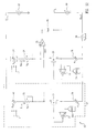
- FIG. 7 a shows a circuit 20 providing temperature compensation in accordance with an embodiment of the present invention.
- Circuit 20 includes supply voltages 22 and 40 , microbolometers 24 and 36 , resistors 26 and 38 , transistor 30 , amplifier 32 , and a digital-to-analog converter (DAC) 34 .
- DAC digital-to-analog converter
- the active microbolometer is the thermally isolated microbolometer 24 that receives incident infrared radiation 1 .
- Microbolometer 24 is biased by supply voltage 22 and a load current (Ibias).
- Amplifier 32 provides the gate bias for transistor 30 (an NMOS transistor), while DAC 34 is used to set a reference voltage and control amplifier 32 to set the appropriate gate bias for transistor 30 .
- amplifier 32 can be eliminated and DAC 34 used to set the appropriate gate bias directly for transistor 30 .
- a load circuit or bias circuit includes supply voltage 40 , resistor 38 , microbolometer 36 , transistor 30 , and amplifier 32 with DAC 34 , which are used to establish the load current (Ibias).
- Microbolometer 36 which is a thermally shorted (to the substrate) load microbolometer, is used as a substrate temperature compensated load.
- Supply voltage 40 is set to optimize the operating point for circuit 20 by setting the nominal voltage drop across microbolometer 36 .
- An output voltage (Vout) 42 of circuit 20 is provided at a node 41 .
- FIG. 7 b shows a circuit 44 for providing temperature compensation in accordance with another embodiment of the present invention.
- Circuit 44 is similar to circuit 20 , but includes an amplifier 28 , which amplifies the voltage at node 41 to provide an output voltage (Vout) 46 .
- Amplifier 28 is an exemplary circuit element to provide amplification or buffering for the voltage at node 41 , if desired.
- a DAC may provide the reference voltage (Vref) for the amplifier or the reference voltage may be at a set voltage level (e.g., ground).
- output voltage (Vout) 42 may be translated, amplified, or converted by amplification or integration processes and/or other well known signal processing techniques. Further references herein to output voltage (Vout) 42 would be also applicable to output voltage (Vout) 46 .
- supply voltage 40 is used to adjust the load current and thereby optimize the operating point of the circuit by setting output voltage 42 at a desired point within a range of output circuitry voltage levels. Specifically, by setting the appropriate gate bias of transistor 30 and appropriate voltage level of supply voltage 40 , the output voltage (Vout) 42 is adjusted.
- supply voltage 40 may be a single voltage level set for the entire array of microbolometers.
- Amplifier 32 and DAC 34 are then used to supply a unique voltage bias to each corresponding thermally-shorted microbolometer 36 in the FPA to provide a fine adjustment or offset to the load voltage or the load current (Ibias). This corrects for the individual offset errors in the output signals from each of the thermally-isolated microbolometers (e.g., microbolometer 24 ).
- the nominal output voltage level of output voltage (Vout) 42 for each circuit is adjusted to fall within a desired range.
- resistors 26 and 38 are provided. Resistor 26 is a variable resistor to generally provide fine adjustments to the composite TCR value of the active microbolometer portion of the circuit relative to the load microbolometer portion of the circuit. Thus, for the voltage divider network of resistors, resistor 26 adjusts the composite TCR of microbolometer 24 and resistor 26 relative to microbolometer 36 and resistor 38 .
- circuit values for these circuit elements are 100 K ⁇ and 300 K ⁇ for microbolometers 24 and 36 , respectively, but these values are not limiting and may vary over a large range, such as for example 50-200 K ⁇ and 150-600 K ⁇ , respectively.
- Exemplary circuit values for resistors 26 and 38 may, for example, vary within 0-10 K ⁇ and 0-30 K ⁇ , respectively, but this range is not limiting and may vary over a wider range of values.
- Resistors 26 and resistors 38 are typically resistors having a different TCR (generally lower) than respective microbolometers 24 and 36 .
- resistor 26 may have a low TCR and microbolometer 24 may have a higher TCR relative to microbolometer 36 . Consequently, by the proper selection of resistance value for resistor 26 , the combination of resistor 26 and microbolometer 24 provides a TCR that is much closer to the TCR of microbolometer 36 than is the TCR of solely microbolometer 24 . Therefore, the performance and behavior of each microbolometer within the array is vastly improved over a range of substrate temperatures.
- the following equation illustrates the combined or composite TCR for a microbolometer in series with a variable resistor (i.e., microbolometer 24 and resistor 26 ) as a function of temperature.
- TCR ( TCR Bo R B ( T )/( R B ( T )+ R Trim ))
- TCR, TCR Bo , R B (T), and R Trim represent the effective combined TCR (labeled TCR), the TCR of the microbolometer (labeled TCR Bo ), the resistance of the microbolometer at a given temperature (labeled R B (T)), and the resistance value of the variable resistor (e.g., to a first order constant as a function of temperature and labeled R Trim ), respectively.
- This equation illustrates how the combined TCR is adjusted depending upon the resistance value of the variable resistor.
- Resistor 38 provides the coarse adjustment for circuit 20 . Consequently by setting resistor 26 , temperature compensation is provided for the mismatch in relative TCR between the active microbolometer and the load microbolometer. A calibration procedure as a function of the substrate temperature is performed to determine the appropriate value for resistors 26 and 38 . Details of an exemplary calibration procedure are provided below.
- the relative mismatch in TCR is driven by various factors, such as pulse bias heating, non-uniformities among microbolometers, and relative contact resistance between the active microbolometer and the load microbolometer and the substrate.
- the characteristics discussed above for FIGS. 3 through 6 are attributable to a certain extent to the relative mismatch in TCR between the load and active microbolometer.
- the output voltage for a given microbolometer circuit will be well behaved as shown in FIG. 8 .
- the microbolometer circuit output voltage falls within a small percentage (e.g., twenty percent) of the minimum and maximum dynamic range over the desired substrate temperature range (e.g., 100° C.).
- FIG. 9 shows a graph of microbolometer circuit output voltage as a function of substrate temperature, which illustrates temperature compensation techniques, in accordance with an embodiment of the present invention.
- Curves 51 through 54 in the figure illustrate, for a given offset, the output voltage for a microbolometer for various resistor trim values (e.g., output voltage 42 for various values of resistor 26 ).
- FIG. 10 shows a graph of microbolometer circuit output voltages from a microbolometer array after implementation of temperature compensation techniques discussed herein. After calibration of a number of microbolometers in the array to compensate for offset and relative mismatch in TCR, all of the microbolometer circuit output voltages fall within a small percentage of dynamic signal range across the desired substrate temperature range. Furthermore, as shown in the histogram in FIG. 11, all of the microbolometer circuit output voltages within the array fall within the available signal range and provide a predictable response.
- the microbolometer FPA performance illustrated in FIGS. 10 and 11 represents a significant improvement over conventional microbolometer FPA performance, such as illustrated respectively in FIGS. 5 and 6.
- resistor 26 and microbolometer 24 may have a lower composite TCR relative to microbolometer 36 , with resistor 26 having a lower TCR than microbolometer 24 .
- Output voltage (Vout) 42 would have a response, for example, such as shown in FIG. 3 .
- the contribution of any resistance by resistor 26 would only further degrade performance due to its low relative TCR.
- resistor 38 which has a lower TCR than microbolometer 36 (the load)
- the composite TCR of resistor 38 and microbolometer 36 is lower than the TCR of microbolometer 24 , producing a curve, for example, as shown in FIG. 4 .
- resistor 26 can then be set, as discussed above, to obtain the desired output response, such as illustrated in FIG. 8 .
- FIGS. 7 a and 7 b is an exemplary circuit to illustrate the relative TCR mismatch and temperature compensation techniques and that numerous modifications and variations are possible in accordance with the principles of the present invention.
- resistor 38 may not be necessary, depending upon the characteristics of the microbolometers within the array.
- Resistors 26 and 38 may be implemented as parallel resistance, rather than series, relative to respective microbolometers, or some combination of series and parallel resistance may be implemented.
- the circuit arrangement may also vary, such as by interchanging the positions of resistor 26 and resistor 38 or the positions of microbolometer 24 and microbolometer 36 .
- one or more techniques discussed or referenced herein may be combined or selectively implemented, depending upon the application or various other factors.
- Circuit 20 in FIG. 7 a (or circuit 44 in FIG. 7 b ) can be implemented in an array configuration, with a portion of circuit 20 placed in the unit cell while the remainder is placed outside of the unit cell, such as in the column amplifier.
- microbolometer 24 may be solely placed within the unit cell (along with associated selection circuitry, such as a row select transistor that is not shown).
- FIG. 12 shows a circuit 60 providing temperature compensation in accordance with another embodiment of the present invention.
- Circuit 60 is similar to circuit 44 of FIG. 7 b , but includes a reference path 62 .
- Reference path 62 includes thermally shorted microbolometers 66 and 74 , variable resistor 68 , a transistor 70 , an amplifier 72 , and a DAC 64 .
- DAC 64 provides a reference voltage to amplifier 72 , which is used to appropriately bias transistor 70 .
- DAC 64 and resistor 68 are adjusted to provide a reference voltage for amplifier 28 .
- Amplifiers 32 and 72 may have their reference voltage provided by a DAC or the reference voltage may be provided to amplifier 32 and/or 72 by a set reference voltage level (e.g., ground).
- microbolometer 66 and/or microbolometer 74 may be replaced by a resistor, which would provide the necessary temperature dependent reference behavior.
- Reference path 62 will be affected by changes in substrate temperature in a similar fashion as the remaining portions of circuit 60 . Consequently, the reference voltage to amplifier 28 will vary in temperature and, therefore, reference path 62 provides additional temperature compensation. Additionally, power supply noise from supply voltages 22 and 40 are reduced by the common mode input to amplifier 28 .
- FIG. 13 shows an exemplary circuit 80 for resistor 26 in accordance with an embodiment of the present invention.
- Circuit 80 includes a number of resistors R 1 through Rn, where n is a number greater than one.
- switches 82 which are separately referenced as 82 ( 1 ) through 82 ( k ), where k is a number greater than one, the desired resistance between nodes 84 and 86 can be set.
- Switches 82 may represent transistors, which could then be switched or controlled by a digital or analog signal. Therefore, circuit 80 provides a variable resistor whose value may be digitally selectable.
- FIG. 14 shows an exemplary enclosure 90 for a microbolometer FPA in accordance with an embodiment of the present invention.
- Enclosure 90 includes an optical element 92 , such as a window or lens, through which incident infrared radiation 1 travels to reach a microbolometer array 98 mounted on a substrate 96 that is physically and thermally secured and attached to a surface 94 of enclosure 90 .
- Optical element 92 may be made, for example, of silicon, germanium, or crystals (e.g., irtran) and enclosure 90 may be made, for example, of ceramic, iron-nickel alloy (e.g., Kovar), or metal or metal alloys (e.g., steel).
- Enclosure 90 contains the microbolometer FPA circuitry and provides appropriate electrical pins, bond pads, or connections to couple to associated electronics, such as to infrared camera electronics.
- thermo-electric cooler In a conventional microbolometer FPA packed assembly with a thermo-electric cooler, there may be a dynamic range degradation due to unwanted infrared radiation transmitted from the enclosure of the microbolometer FPA if the enclosure were to have a change in temperature independently from the sensor (e.g., FPA).
- infrared radiation such as from enclosure 90 is factored into the calibration process and accounted for, which reduces the associated dynamic range degradation.
- FIG. 15 is a top-level flowchart 100 of a calibration process in accordance with an embodiment of the present invention.
- Flowchart 100 includes steps 102 through 110 for calibrating a microbolometer FPA.
- Step 104 is a required step and steps 102 and 106 through 110 may be optional steps, depending upon the microbolometer FPA behavior or performance, the desired application, and required performance.
- FIGS. 16 through 19 provide exemplary detailed flowcharts pertaining to steps 102 through 110 .
- the external resistance is calibrated in step 102 .
- the term “external resistance” refers, for example, to the resistance of a resistor such as resistor 38 of FIG. 7 a , which is typically placed outside of the unit cell and is not part of the variable (or trim) resistance (e.g., resistor 26 of FIG. 7 a ).
- the external resistance or the value of the external resistor may be digitally selectable and/or may be a global resistor and may be on or off-chip (i.e., on or off the FPA or the ROIC). Therefore, one external variable resistor or a few external variable resistors may be sufficient for a large microbolometer FPA.
- the global external resistor is set to its calibrated value, determined during the calibration process, corresponding to that particular microbolometer, column, group, or array of microbolometers.
- an external resistor may not be required depending upon the behavior of the microbolometers in the FPA.
- the variable resistance and offset is calibrated for each microbolometer in step 104 .
- the variable resistance or trim resistance refers, for example, to the resistance of a resistor (a trim resistor) such as resistor 26 in FIG. 7 a .
- step 104 determines the amount of resistance to be placed in series with each microbolometer in the FPA.
- Step 104 also determines the amount of offset to be applied for each microbolometer in the FPA.
- the determined offset for each microbolometer may be set by using DAC 34 to control the gate bias of transistor 30 via amplifier 32 in FIG. 7 a.
- Step 106 provides fine offset correction calibration for each microbolometer circuit output over the desired substrate temperature range.
- Various techniques may be employed to provide a fine correction to each microbolometer circuit output after step 104 and possibly step 102 are performed, because these steps then provide a correctable microbolometer circuit output over a wide range of substrate temperature.
- the techniques may include various mathematical best-fit or offset correction algorithms or look-up table methods to determine the fine offset correction factor for a given temperature. For example, Lagrange terms enable a polynomial offset correction to be generated in real-time for each microbolometer that compensates for variations in microbolometer circuit output over FPA substrate temperature.
- Step 108 provides gain calibration for each microbolometer.
- the gain terms normalize the response of each microbolometer to incident infrared radiation. This step may simply determine the gain term independent of FPA substrate temperature or, in a more general fashion, determine the gain term as a function of FPA substrate temperature. Similar mathematical best-fit, correction algorithms, or look-up table methods can be provided for these terms.
- Step 110 provides an additional fine offset, if required, for each microbolometer. The offset also may be a function of FPA substrate temperature.
- FIG. 16 is a detailed flowchart 120 for step 102 of flowchart 100 in FIG. 15 .
- Flowchart 120 provides exemplary calibrations steps for calibrating the external resistor.
- Step 122 sets the trim resistor for each microbolometer to a target value, such as the mean value of the trim resistor.
- the FPA temperature is then set to a value (i.e., T 1 ) within the desired calibration or operation temperature range (step 124 ).
- T 1 may represent the value of the minimum operating temperature range.
- the external resistor is then set to one of its “n” possible values (step 126 ) and the offset is calibrated for each microbolometer (step 128 ), where the offset may be calibrated using the procedure described below.
- the offset value and microbolometer circuit output value, obtained after application of the offset value, is stored (step 130 ) and steps 126 through step 128 are repeated for each of the n possible external resistor values (step 132 ).
- the result is n pairs of external resistor and offset values along with each corresponding microbolometer circuit output value.
- the FPA temperature is then changed to another value (e.g., T 2 ) within the desired calibration range (step 134 ).
- the stored external resistor and offset values are applied, for each value of n, and the microbolometer circuit output value is recorded (step 136 ).
- step 138 calculates the difference between the microbolometer circuit output from step 136 (i.e., at T 1 ) and the microbolometer circuit output from step 132 (i.e., at T 2 ) and then calculates the average difference across the full array of microbolometers.
- Step 140 selects the external resistor value corresponding to the smallest average difference obtained from step 138 , with this resistor value being the calibrated value of the external resistor for the entire microbolometer FPA.
- FIG. 17 is a detailed flowchart 150 for the trim resistance calibration in step 104 of flowchart 100 in FIG. 15 .
- Flowchart 150 provides exemplary calibration steps for calibrating the trim resistor.
- Step 152 sets the FPA substrate temperature to one extreme of the desired operating or calibration temperature range (e.g., T 1 ).
- the trim resistor is set to one of “m” possible values (step 154 ), such as the minimum value, and then the offset is calibrated (step 156 ) using a procedure, such as the one described below.
- the offset value and the resulting microbolometer circuit output value, after application of the offset value, are recorded for the given trim resistor value (step 158 ).
- Step 160 repeats steps 154 through 158 for each of the m possible trim resistor values, which results in m pairs of trim resistor/offset values and corresponding microbolometer circuit output values.
- FIG. 20 shows a graph and accompanying table illustrating a calibration operation in accordance with an embodiment of the present invention.
- FIG. 20 provides an exemplary illustration of the trim resistor calibration through step 160 of flowchart 150 for a single microbolometer and three possible trim resistor values (i.e., m equals three).
- the microbolometer circuit output (or pixel output) is plotted for a given FPA substrate temperature (T 1 ).
- the accompanying table provides a tabulation of trim resistor value (RDAC value), offset value (ODAC value), and pixel output value at temperature T 1 for the three trim resistor values.
- the labels “RDAC value” and “ODAC value” refer to the resistor and offset values being digitally selectable or controlled, as discussed above and illustrated in the figures.
- the pixel output value is listed as a percentage of the microbolometer circuit output dynamic range or desired output range.
- FIG. 21 shows a graph and accompanying table, illustrating step 164 , in accordance with an embodiment of the present invention.
- FIG. 21 is similar to FIG. 20, but now includes the three exemplary microbolometer circuit output values obtained at temperature T2.
- Step 166 For each value of m (FIG. 17 —step 166 ), the difference is calculated between the microbolometer circuit output from step 164 (i.e., at temperature T2) and the microbolometer circuit output obtained from step 158 (i.e., at temperature T 1 ).
- Step 168 selects the trim resistor value and associated offset value that corresponds to the minimum difference from the results of step 166 . These values are the calibrated values for the trim resistor and offset. Note that, if desired, the offset can be re-calibrated at a different FPA temperature value or with a different target value. This would provide a wider temperature operating range and more well-behaved performance.
- FIG. 22 shows a graph and accompanying table illustrating steps 166 and 168 in accordance with an embodiment of the present invention.
- FIG. 22 is similar to FIG. 21, but now includes the difference calculation of values between the two temperature settings and the selection of the trim resistor/offset that generates the minimum difference.
- the offset value is determined for each microbolometer in the FPA.
- the offset value for example, can be determined for each microbolometer by using a binary search to find the offset value that adjusts the microbolometer circuit output value closest to a desired value (i.e., microbolometer circuit output target value).
- the temperature of the FPA substrate and other parameters, such as the flux incident on the FPA, should generally not vary substantially while the offset calibration is in process.
- FIG. 18 is a detailed flowchart 180 for step 106 of flowchart 100 in FIG. 15 .
- Flowchart 180 provides exemplary calibrations steps for calibrating the fine offset correction (e.g., Lagrange) terms for a microbolometer in the FPA array.
- the exemplary procedure could be employed in the more general case to calibrate many pixels simultaneously.
- Step 182 sets the FPA temperature to a value within the desired calibration or operating range and records the measured temperature value (having temperature units, such as Kelvin or Celsius, or units of volts that correspond to a given temperature). For this temperature, the microbolometer circuit output is recorded after the application of the calibrated trim resistor and offset values (step 184 ).
- Step 186 The FPA temperature is then changed, at step 186 , to another value within the desired temperature range and steps 182 and 184 are repeated.
- Step 188 repeats step 186 a minimum of K+1 times, where K represents the desired order of the polynomial correction. For example, a minimum of four terms is stored if the third order polynomial correction is desired.
- the polynomial correction results generally improve if two of the K+1 points are at the opposite extremes of the desired calibration range.
- the gain of each microbolometer can be calibrated using a two-point calibration process (e.g., at two different values of incident flux) at any arbitrary FPA temperature.
- the gain of each microbolometer can be calibrated as a function of FPA temperature, such as in the calibration process described below. Both procedures are similar to the fine offset (e.g., Lagrange) correction described above in reference to FIG. 18, but the two procedures (i.e., gain and fine offset) differ from each other in that instead of storing each microbolometer circuit output at a single value of incident flux, each microbolometer circuit output is stored for two values of incident flux.
- FIG. 19 is a detailed flowchart 200 for step 108 of flowchart 100 in FIG. 15 .
- Flowchart 200 provides exemplary calibration steps for calibrating the gain of each microbolometer.
- Step 202 sets the FPA temperature to a value within the desired calibration or operating range and the temperature value is recorded (in units of temperature, such as Kelvin or Celsius, or in units of voltage that correspond to a given temperature).
- Step 204 records the microbolometer circuit output difference for two flux levels or responsivity for that temperature for each microbolometer.
- Step 206 changes the FPA temperature to another value within the calibration or operating range and the temperature value and each microbolometer circuit output is recorded.
- Step 206 is repeated (in step 208 ) a minimum of K+1 times, where k represents the desired order of the polynomial fit of the gain terms.
- FIG. 23 illustrates a compensation process 220 in accordance with an embodiment of the present invention.
- Compensation process 220 illustrates generally the overall compensation process for providing an optimal output from each microbolometer in the FPA over the desired FPA temperature range.
- the microbolometer FPA is represented symbolically by an FPA 222 .
- each microbolometer in the array receives a trim resistor (Rtrim i , where i ranges from 1 ⁇ i ⁇ maximum number of microbolometers in the array) and an offset calibration (Offset i ) adjustment.
- the trim resistor calibration and the offset calibration adjust each microbolometer circuit output over the calibrated temperature range from, for example, what is shown in FIGS. 3 or 4 to what is shown in FIG. 8 .
- An external resistor (Rext) calibration is also optionally performed as described above, depending upon microbolometer FPA behavior. There may be an external resistor digitally selectable for each microbolometer or there may be one global external resistor that is calibrated for the entire microbolometer FPA.
- the microbolometer circuit outputs from FPA 222 are combined in block 224 with the calibrated temperature-dependent fine (e.g., Lagrange) offset 230 .
- the fine offset may be determined in any of a number of methods or techniques, as discussed herein.
- FIG. 23 refers to the fine offset as Lagrange offset 230 , which is one exemplary method, but the fine offset is not intended to be limited solely to this exemplary method.
- Lagrange offset 230 provides the calibrated polynomial correction values for each microbolometer circuit output, which can be summed with each microbolometer circuit output from FPA 222 . As shown in FIGS.
- the microbolometer circuit outputs over the calibrated temperature range tend to produce a curved or bowed output curve, after application of the trim resistor, offset, and possibly external resistor calibrated values.
- the application of Lagrange offset 230 refines the microbolometer circuit output behavior and provides a more uniform output (i.e., reduces the curve or bow in microbolometer circuit output over temperature).
- Lagranae offset 230 receives as inputs the measured substrate temperature and the Lagrange terms (Lagrange Term i ), which are used to generate the Lagrange offset terms uniquely for each microbolometer in the array.
- a block 226 receives the microbolometer circuit outputs, after application of the Lagrange offsets, and multiplies the microbolometer circuit outputs by a corresponding calibrated temperature dependent gain 232 .
- the gain adjusts each microbolometer circuit output to provide a more uniform response to incident flux. As shown, the gain is temperature dependent and receives as inputs the measured substrate temperature and the gain terms (Gain Term i ), which are used to generate the temperature dependent gain uniquely for each microbolometer in the array.
- a block 228 receives the microbolometer circuit outputs, after application of the gain adjustment, and sums the microbolometer circuit outputs with additional offset terms (Offset i ), with the offset for block 228 typically differing from the offset input to FPA 222 .
- the offset term is updated periodically during camera operation using a shutter, a chopper, or a scene-based algorithm.
- the implementation of the trim resistor within each microbolometer circuit provides the correctable microbolometer FPA performance over a wide temperature range.
- the correctable microbolometer FPA performance over the calibrated temperature range then permits the application of Lagrange offset, gain, and offset calibration over the wide calibrated temperature range.
- the principles of this invention may be implemented or applied to a wide variety of circuit devices and materials. Accordingly, the embodiments described herein are only exemplary of the principles of the invention and are not intended to limit the invention to the specific embodiments disclosed.
- FIG. 24 shows a circuit 240 for providing temperature compensation in accordance with another embodiment of the present invention.
- Circuit 240 is similar to circuit 44 of FIG. 7 b , but illustrates that the voltage reference for amplifier 28 can be provided by a DAC 242 .
- DAC 242 can be controlled to provide a varying voltage reference level, for example based on the measured substrate temperature.
- Amplifier 32 may have its positive input terminal tied to a ground voltage level (as shown in FIG. 24) or set by DAC 34 (as shown in FIG. 7 b ).
- FIG. 25 shows a circuit 250 for providing temperature compensation in accordance with another embodiment of the present invention.
- Circuit 250 includes supply voltages 22 and 40 , microbolometers 24 and 36 , resistors 26 and 38 , transistors 30 and 252 , DACs 254 and 256 , an amplifier 258 , an impedance element (e.g., a switched capacitor network) 260 , and output voltage (Vout) 46 .
- an impedance element e.g., a switched capacitor network
- Vout output voltage
- Resistors 26 and 38 , microbolometers 24 and 36 , and supply voltages 22 and 40 operate in a similar manner as discussed above in reference to FIG. 7 a and therefore the description will not be repeated.
- DACs 254 and 256 are coupled to the gate terminals of transistors 252 and 30 , respectively, to control the bias applied to microbolometers 24 and 36 , respectively. Specifically, DAC 254 adjusts the offset by controlling the bias applied to microbolometer 24 in combination with resistor 26 via transistor 252 . DAC 256 adjusts the offset by controlling the bias applied to microbolometer 36 in series with resistor 38 via transistor 30 .
- Amplifier 258 and impedance element 260 form a transimpedance amplifier, which translates the current level flowing into the transimpedance amplifier into a voltage level at output voltage (Vout) 46 . Consequently, DACs 254 and 256 determine the amount of current flowing through respective microbolometers 24 and 36 and also into the transimpedance amplifier and, thus, set the offset and reference level of output voltage (Vout) 46 .
- DACs 254 and 256 can be calibrated, as discussed above, for a single temperature or over a desired operating temperature range for each microbolometer in the FPA array.
- FIG. 26 shows a circuit 270 for providing temperature compensation in accordance with another embodiment of the present invention.
- Circuit 270 is similar to circuit 250 of FIG. 25, but a current source 272 is provided and resistor 26 is eliminated.
- the amount of current flowing through microbolometer 24 to produce a microbolometer bias current (IbiasB) is reduced by the contribution of current by current source 272 . Therefore, the voltage across microbolometer 24 is reduced and the change in the contribution of current (Ibolo) through microbolometer 24 to the microbolometer bias current (IbiasB) as a function of temperature is fractionally reduced.
- current source 272 has effectively lowered the TCR of microbolometer 24 .
- FIG. 27 shows a microbolometer readout integrated circuit with bias-correction circuitry and interface system electronics in accordance with an embodiment of the present invention.
- FIG. 27 includes a readout integrated circuit (ROIC) 282 that includes the microbolometer FPA, control circuitry, timing circuitry, bias circuitry, row and column addressing circuitry, column amplifiers, and associated electronics to provide output signals that are digitized by an analog-to-digital (A/D) converter 284 .
- the A/D converter 284 may be located on or off ROIC ( 282 ).
- the output signals from A/D converter 284 are adjusted by a non-uniformity correction circuit (NUC) 285 , which applies temperature dependent compensation (e.g., Lagrange Offset, Temperature Dependent Gain, and additional Offset) as discussed above, such as in reference to FIG. 23 .
- NUC non-uniformity correction circuit
- the output signals are stored in a frame memory 286 .
- the data in frame memory 286 is then available to image display electronics 288 and a data processor 292 , which also has a data processor memory 290 .
- a timing generator 294 provides system timing.
- Data processor 292 generates bias-correction data words, which are loaded into a correction coefficient memory 298 .
- a data register load circuitry 296 provides the interface to load the correction data into readout integrated circuit 282 .
- the variable resistors, digital-to-analog converters, and other variable circuitry, which control voltage levels, biasing, circuit element values, etc., are controlled by data processor 292 so that the output signals from readout integrated circuit are uniform over a wide temperature range.
Abstract
Description
Claims (58)
Priority Applications (6)
| Application Number | Priority Date | Filing Date | Title |
|---|---|---|---|
| US10/085,226 US6812465B2 (en) | 2002-02-27 | 2002-02-27 | Microbolometer focal plane array methods and circuitry |
| JP2003571695A JP3961486B2 (en) | 2002-02-27 | 2003-02-24 | Microbolometer focal plane array method and circuit |
| EP03713621.5A EP1478909B1 (en) | 2002-02-27 | 2003-02-24 | Microbolometer focal plane array methods and circuitry |
| AU2003217664A AU2003217664A1 (en) | 2002-02-27 | 2003-02-24 | Microbolometer focal plane array methods and circuitry |
| PCT/US2003/005455 WO2003073054A2 (en) | 2002-02-27 | 2003-02-24 | Microbolometer focal plane array methods and circuitry |
| US10/761,769 US7034301B2 (en) | 2002-02-27 | 2004-01-20 | Microbolometer focal plane array systems and methods |
Applications Claiming Priority (1)
| Application Number | Priority Date | Filing Date | Title |
|---|---|---|---|
| US10/085,226 US6812465B2 (en) | 2002-02-27 | 2002-02-27 | Microbolometer focal plane array methods and circuitry |
Related Child Applications (1)
| Application Number | Title | Priority Date | Filing Date |
|---|---|---|---|
| US10/761,769 Continuation-In-Part US7034301B2 (en) | 2002-02-27 | 2004-01-20 | Microbolometer focal plane array systems and methods |
Publications (2)
| Publication Number | Publication Date |
|---|---|
| US20030160171A1 US20030160171A1 (en) | 2003-08-28 |
| US6812465B2 true US6812465B2 (en) | 2004-11-02 |
Family
ID=27753585
Family Applications (1)
| Application Number | Title | Priority Date | Filing Date |
|---|---|---|---|
| US10/085,226 Expired - Lifetime US6812465B2 (en) | 2002-02-27 | 2002-02-27 | Microbolometer focal plane array methods and circuitry |
Country Status (5)
| Country | Link |
|---|---|
| US (1) | US6812465B2 (en) |
| EP (1) | EP1478909B1 (en) |
| JP (1) | JP3961486B2 (en) |
| AU (1) | AU2003217664A1 (en) |
| WO (1) | WO2003073054A2 (en) |
Cited By (56)
| Publication number | Priority date | Publication date | Assignee | Title |
|---|---|---|---|---|
| US20070194237A1 (en) * | 2006-02-21 | 2007-08-23 | Redshift Systems Corporation | Thermo-optic system employing self reference |
| US7402803B1 (en) | 2005-06-07 | 2008-07-22 | Redshift Systems Corporation | Pixel architecture for thermal imaging system |
| US20090014653A1 (en) * | 2007-07-12 | 2009-01-15 | Parrish William J | Bolometer array compensation |
| US20090134330A1 (en) * | 2007-11-26 | 2009-05-28 | Fraunhofer-Gesellschaft Zur Foerderung Der Angewandten Forschung E.V. | Concept for determining a measurement value at a component |
| US8049163B1 (en) | 2008-09-02 | 2011-11-01 | Flir Systems, Inc. | Calibration systems and methods for infrared cameras |
| US8080794B1 (en) | 2009-06-17 | 2011-12-20 | Flir Systems, Inc. | Microbolometer heating compensation systems and methods |
| CN101339074B (en) * | 2007-07-02 | 2011-12-28 | Ulis股份公司 | Device for detecting infrared radiation using bolometric detectors |
| US8158943B2 (en) | 2009-04-12 | 2012-04-17 | Ud Holdings, Llc | Infrared detector |
| WO2012170941A1 (en) | 2011-06-10 | 2012-12-13 | Flir Systems, Inc. | Infrared camera system architectures |
| WO2012170953A2 (en) | 2011-06-10 | 2012-12-13 | Flir Systems, Inc. | Systems and methods for intelligent monitoring of thoroughfares using thermal imaging |
| WO2012170949A2 (en) | 2011-06-10 | 2012-12-13 | Flir Systems, Inc. | Non-uniformity correction techniques for infrared imaging devices |
| WO2012170954A2 (en) | 2011-06-10 | 2012-12-13 | Flir Systems, Inc. | Line based image processing and flexible memory system |
| WO2012170946A2 (en) | 2011-06-10 | 2012-12-13 | Flir Systems, Inc. | Low power and small form factor infrared imaging |
| US8373757B1 (en) | 2009-02-23 | 2013-02-12 | Flir Systems, Inc. | Flat field correction for infrared cameras |
| US8378290B1 (en) * | 2008-09-02 | 2013-02-19 | Flir Systems, Inc. | Sensor calibration systems and methods for infrared cameras |
| US8395118B2 (en) | 2009-04-12 | 2013-03-12 | Ud Holdings, Llc | Infrared detector having at least one switch for modulation and/or bypass |
| WO2013052383A1 (en) | 2011-10-07 | 2013-04-11 | Flir Systems, Inc. | Smart surveillance camera systems and methods |
| WO2013052196A1 (en) | 2011-10-07 | 2013-04-11 | Flir Systems, Inc. | Determination of an absolute radiometric value using blocked infrared sensors |
| US8471206B1 (en) | 2009-07-14 | 2013-06-25 | Flir Systems, Inc. | Infrared detector vacuum test systems and methods |
| US8552375B1 (en) | 2009-06-17 | 2013-10-08 | Flir Systems, Inc. | Switched capacitor filter systems and methods |
| WO2013152122A2 (en) | 2012-04-06 | 2013-10-10 | Flir Systems, Inc. | Electrical cabinet infrared monitor |
| US8587637B1 (en) | 2010-05-07 | 2013-11-19 | Lockheed Martin Corporation | Three dimensional ladar imaging and methods using voxels |
| WO2013184220A2 (en) | 2012-03-19 | 2013-12-12 | Flir Systems, Inc. | Wearable apparatus with integrated infrared imaging module |
| WO2014012070A1 (en) | 2012-07-12 | 2014-01-16 | Flir Systems, Inc. | Infant monitoring systems and methods using thermal imaging |
| WO2014043592A2 (en) | 2012-09-14 | 2014-03-20 | Flir Systems, Inc. | Measurement device for electrical installations and related methods |
| WO2014047076A1 (en) | 2012-09-18 | 2014-03-27 | Flir Systems, Inc. | Pixel-wise noise reduction in thermal images |
| US8729474B1 (en) | 2009-10-09 | 2014-05-20 | Flir Systems, Inc. | Microbolometer contact systems and methods |
| WO2014082097A1 (en) | 2012-11-26 | 2014-05-30 | Flir Systems, Inc. | Hybrid infrared sensor array having heterogeneous infrared sensors |
| WO2014085699A1 (en) | 2012-11-27 | 2014-06-05 | Flir Systems, Inc. | Infrared imager with integrated metal layers |
| WO2014093721A2 (en) | 2012-12-14 | 2014-06-19 | Flir Systems, Inc. | Abnormal clock rate detection in imaging sensor arrays |
| WO2014093724A1 (en) | 2012-12-14 | 2014-06-19 | Flir Systems, Inc. | Segmented focal plane array architecture |
| WO2014100507A2 (en) | 2012-12-21 | 2014-06-26 | Flir Systems, Inc. | Systems and methods for monitoring power systems |
| WO2014100741A2 (en) | 2012-12-21 | 2014-06-26 | Flir Systems, Inc. | Systems and methods of suppressing sky regions in images |
| WO2014100784A1 (en) | 2012-12-21 | 2014-06-26 | Flir Systems, Inc. | Infrared imaging enhancement with fusion |
| WO2014100786A1 (en) | 2012-12-21 | 2014-06-26 | Flir Systems, Inc. | Selective image correction for infrared imaging devices |
| WO2014105904A1 (en) | 2012-12-26 | 2014-07-03 | Flir Systems, Inc. | Infrared focal plane array heat spreaders |
| WO2014105897A1 (en) | 2012-12-26 | 2014-07-03 | Flir Systems, Inc. | Infrared detector array with selectable pixel binning systems and methods |
| WO2014106276A2 (en) | 2012-12-31 | 2014-07-03 | Flir Systems, Inc. | Infrared imaging device having a shutter |
| WO2014105241A1 (en) | 2012-12-26 | 2014-07-03 | Flir Systems, Inc. | Device attachment with infrared imaging sensor |
| WO2014105993A1 (en) | 2012-12-26 | 2014-07-03 | Flir Systems, Inc. | Electrical cabinet infrared monitor systems and methods |
| WO2014106278A1 (en) | 2012-12-31 | 2014-07-03 | Flir Systems, Inc. | Anomalous pixel detection |
| WO2014143338A2 (en) | 2012-12-21 | 2014-09-18 | Flir Systems, Inc. | Imager with array of multiple infrared imaging modules |
| US8946640B2 (en) | 2010-12-23 | 2015-02-03 | Flir Systems, Inc. | Unit cells with avalanche photodiode detectors |
| WO2015051344A1 (en) | 2013-10-03 | 2015-04-09 | Flir Systems, Inc. | Durable compact multisensor observation devices |
| WO2015058166A2 (en) | 2013-10-18 | 2015-04-23 | Flir Systems, Inc. | Measurement device for lighting installations and related methods |
| US9052381B2 (en) | 2010-05-07 | 2015-06-09 | Flir Systems, Inc. | Detector array for high speed sampling of an optical pulse |
| WO2015123143A1 (en) | 2014-02-11 | 2015-08-20 | Flir Systems, Inc. | Measurement device with thermal imaging capabilities and related methods |
| WO2016176370A1 (en) | 2015-04-27 | 2016-11-03 | Flir Systems, Inc. | Moisture measurement device with thermal imaging capabilities and related methods |
| US9491376B2 (en) | 2009-02-23 | 2016-11-08 | Flir Systems, Inc. | Flat field correction for infrared cameras |
| US9658111B2 (en) | 2009-10-09 | 2017-05-23 | Flir Systems, Inc. | Microbolometer contact systems and methods |
| US9958332B2 (en) | 2014-10-16 | 2018-05-01 | Flir Systems, Inc. | Bolometer circuitry and methods for difference imaging |
| WO2018156668A1 (en) | 2017-02-22 | 2018-08-30 | Flir Systems, Inc. | Low cost and high performance bolometer circuitry and methods |
| WO2018156661A1 (en) | 2017-02-22 | 2018-08-30 | Flir Systems, Inc. | Low cost and high performance bolometer circuitry and methods |
| WO2020185969A2 (en) | 2019-03-11 | 2020-09-17 | Flir Commercial Systems, Inc. | Microbolometer systems and methods |
| WO2021211755A1 (en) | 2020-04-17 | 2021-10-21 | Flir Commercial Systems, Inc. | Bolometer unit cell pixel integrity check systems and methods |
| US11543297B2 (en) | 2019-07-19 | 2023-01-03 | Industrial Technology Research Institute | Sensing devices |
Families Citing this family (22)
| Publication number | Priority date | Publication date | Assignee | Title |
|---|---|---|---|---|
| US7034301B2 (en) * | 2002-02-27 | 2006-04-25 | Indigo Systems Corporation | Microbolometer focal plane array systems and methods |
| US7274915B2 (en) | 2003-08-29 | 2007-09-25 | Broadcom Corporation | Low-noise transmitter system and method |
| JP2008185465A (en) | 2007-01-30 | 2008-08-14 | Nec Electronics Corp | Method and apparatus for compensating infrared sensor for temperature |
| US7772557B2 (en) * | 2007-03-29 | 2010-08-10 | Fluke Corporation | Offset compensation scheduling algorithm for infrared imagers |
| FR2918746B1 (en) * | 2007-07-13 | 2009-10-09 | Commissariat Energie Atomique | ELECTRONIC SENSOR WITH INTEGRATED THERMAL CONTROL |
| FR2925158B1 (en) * | 2007-12-12 | 2011-07-01 | Ulis | DEVICE FOR THE DETECTION OF ELECTROMAGNETIC RADIATION COMPRISING A RESISTIVE IMAGING BOLOMETER, SYSTEM COMPRISING A MATRIX OF SUCH DEVICES AND METHOD FOR READING AN IMAGING BOLOMETER OF SUCH A SYSTEM |
| US7679048B1 (en) | 2008-04-18 | 2010-03-16 | Flir Systems, Inc. | Systems and methods for selecting microbolometers within microbolometer focal plane arrays |
| FR2934679B1 (en) * | 2008-07-29 | 2010-09-24 | Ulis | DEVICE AND METHOD FOR DETECTING INFRARED RADIATION USING A RESISTIVE BOLOMETER MATRIX. |
| US8704180B2 (en) | 2008-07-29 | 2014-04-22 | Ulis | Device and method for detecting infrared radiation through a resistive bolometer matrix |
| FR2941046B1 (en) * | 2009-01-15 | 2011-02-18 | Ulis | DEVICE FOR DETECTING ELECTROMAGNETIC RADIATION |
| FR2941298B1 (en) * | 2009-01-19 | 2011-02-18 | Ulis | DEVICE FOR DETECTING ELECTROMAGNETIC RADIATION AND ELECTROMAGNETIC RADIATION DETECTOR HAVING SUCH DEVICES. |
| FR2951895B1 (en) * | 2009-10-22 | 2012-07-13 | Ulis | METHOD OF CORRECTING IMAGES DELIVERED BY A DETECTOR NOT REGULATED IN TEMPERATURE, AND DETECTOR USING SUCH A METHOD |
| FR2969763B1 (en) * | 2010-12-22 | 2013-02-15 | Commissariat Energie Atomique | MEASURING SYSTEM AND IMAGER HAVING SUCH A SYSTEM |
| US9167179B2 (en) | 2011-02-21 | 2015-10-20 | Vectronix, Inc. | On-board non-uniformity correction calibration methods for microbolometer focal plane arrays |
| JP5542090B2 (en) * | 2011-04-27 | 2014-07-09 | 旭化成エレクトロニクス株式会社 | Infrared sensor signal correction method, temperature measurement method, and temperature measurement apparatus |
| JP5932535B2 (en) * | 2012-07-17 | 2016-06-08 | 浜松ホトニクス株式会社 | measuring device |
| FR3009388B1 (en) | 2013-07-30 | 2015-07-17 | Ulis | DIAGNOSIS OF THE DEFECTIVE STATE OF A BOLOMETRIC DETECTION MATRIX |
| FR3015666B1 (en) * | 2013-12-19 | 2017-02-03 | Commissariat Energie Atomique | MEASUREMENT CIRCUIT FOR BOLOMETRIC DETECTOR |
| CN109738073B (en) * | 2019-01-28 | 2020-01-17 | 北京安酷智芯科技有限公司 | Non-uniformity correction circuit and correction bias voltage generation circuit |
| CN113906275B (en) * | 2019-06-12 | 2023-12-22 | 三菱电机株式会社 | Infrared shooting device |
| US11594532B2 (en) * | 2020-06-29 | 2023-02-28 | Texas Instruments Incorporated | On-chip heater temperature calibration |
| CN111982311B (en) * | 2020-07-15 | 2021-10-12 | 北京北方高业科技有限公司 | Non-uniform correction circuit and method for barrier-free infrared detector and infrared detector |
Citations (12)
| Publication number | Priority date | Publication date | Assignee | Title |
|---|---|---|---|---|
| US4947057A (en) | 1987-09-09 | 1990-08-07 | Motorola, Inc. | Adjustable temperature variable output signal circuit |
| US5756999A (en) * | 1997-02-11 | 1998-05-26 | Indigo Systems Corporation | Methods and circuitry for correcting temperature-induced errors in microbolometer focal plane array |
| US6028309A (en) * | 1997-02-11 | 2000-02-22 | Indigo Systems Corporation | Methods and circuitry for correcting temperature-induced errors in microbolometer focal plane array |
| US6267501B1 (en) * | 1999-03-05 | 2001-07-31 | Raytheon Company | Ambient temperature micro-bolometer control, calibration, and operation |
| US6300616B1 (en) * | 1998-12-22 | 2001-10-09 | Diehl Stiftung & Co. | Detector circuit with a stationary potential amplifier input |
| US6359460B1 (en) * | 1998-10-06 | 2002-03-19 | Nec Corporation | Semiconductor memory device |
| US20020040967A1 (en) * | 2000-08-29 | 2002-04-11 | Nec Corporation | Thermo-sensitive infrared ray detector |
| US6441372B1 (en) * | 1998-10-05 | 2002-08-27 | Nec Corporation | Infrared focal plane array detector and method of producing the same |
| US20030006374A1 (en) * | 2000-05-05 | 2003-01-09 | Mcmanus Timothy J. | Apparatus and method for compensating for pixel non-uniformity in a bolometer |
| US20030122077A1 (en) * | 2001-05-11 | 2003-07-03 | Kaufman Charles S. | Method and apparatus for temperature compensation of an uncooled focal plane array |
| US20030146383A1 (en) * | 2000-03-17 | 2003-08-07 | Knauth Jonathan P. | Method and apparatus for correction of microbolometer output |
| US20030213910A1 (en) * | 1999-10-07 | 2003-11-20 | Anderson Shane M. | Microbolometer focal plane array with temperature compensated bias |
-
2002
- 2002-02-27 US US10/085,226 patent/US6812465B2/en not_active Expired - Lifetime
-
2003
- 2003-02-24 JP JP2003571695A patent/JP3961486B2/en not_active Expired - Lifetime
- 2003-02-24 EP EP03713621.5A patent/EP1478909B1/en not_active Expired - Lifetime
- 2003-02-24 AU AU2003217664A patent/AU2003217664A1/en not_active Abandoned
- 2003-02-24 WO PCT/US2003/005455 patent/WO2003073054A2/en active Application Filing
Patent Citations (12)
| Publication number | Priority date | Publication date | Assignee | Title |
|---|---|---|---|---|
| US4947057A (en) | 1987-09-09 | 1990-08-07 | Motorola, Inc. | Adjustable temperature variable output signal circuit |
| US5756999A (en) * | 1997-02-11 | 1998-05-26 | Indigo Systems Corporation | Methods and circuitry for correcting temperature-induced errors in microbolometer focal plane array |
| US6028309A (en) * | 1997-02-11 | 2000-02-22 | Indigo Systems Corporation | Methods and circuitry for correcting temperature-induced errors in microbolometer focal plane array |
| US6441372B1 (en) * | 1998-10-05 | 2002-08-27 | Nec Corporation | Infrared focal plane array detector and method of producing the same |
| US6359460B1 (en) * | 1998-10-06 | 2002-03-19 | Nec Corporation | Semiconductor memory device |
| US6300616B1 (en) * | 1998-12-22 | 2001-10-09 | Diehl Stiftung & Co. | Detector circuit with a stationary potential amplifier input |
| US6267501B1 (en) * | 1999-03-05 | 2001-07-31 | Raytheon Company | Ambient temperature micro-bolometer control, calibration, and operation |
| US20030213910A1 (en) * | 1999-10-07 | 2003-11-20 | Anderson Shane M. | Microbolometer focal plane array with temperature compensated bias |
| US20030146383A1 (en) * | 2000-03-17 | 2003-08-07 | Knauth Jonathan P. | Method and apparatus for correction of microbolometer output |
| US20030006374A1 (en) * | 2000-05-05 | 2003-01-09 | Mcmanus Timothy J. | Apparatus and method for compensating for pixel non-uniformity in a bolometer |
| US20020040967A1 (en) * | 2000-08-29 | 2002-04-11 | Nec Corporation | Thermo-sensitive infrared ray detector |
| US20030122077A1 (en) * | 2001-05-11 | 2003-07-03 | Kaufman Charles S. | Method and apparatus for temperature compensation of an uncooled focal plane array |
Non-Patent Citations (3)
| Title |
|---|
| International Preliminary Exaimination Report for PCT/US03/05455. |
| International Search Report for PCT/US03/05455. |
| Written Opinion for PCT/US03/05455. |
Cited By (72)
| Publication number | Priority date | Publication date | Assignee | Title |
|---|---|---|---|---|
| US7402803B1 (en) | 2005-06-07 | 2008-07-22 | Redshift Systems Corporation | Pixel architecture for thermal imaging system |
| US20090026370A1 (en) * | 2005-06-07 | 2009-01-29 | Redshift Systems Corporation | Pixel architecture for thermal imaging system |
| US7829854B2 (en) | 2005-06-07 | 2010-11-09 | Redshift Systems Corporation | Pixel architecture for thermal imaging system |
| US7750300B2 (en) | 2006-02-21 | 2010-07-06 | Redshift Systems Corporation | Thermo-optic system employing self reference |
| US20070194237A1 (en) * | 2006-02-21 | 2007-08-23 | Redshift Systems Corporation | Thermo-optic system employing self reference |
| CN101339074B (en) * | 2007-07-02 | 2011-12-28 | Ulis股份公司 | Device for detecting infrared radiation using bolometric detectors |
| US7709793B2 (en) | 2007-07-12 | 2010-05-04 | Parrish William J | Bolometer array compensation |
| US20090014653A1 (en) * | 2007-07-12 | 2009-01-15 | Parrish William J | Bolometer array compensation |
| US8692199B2 (en) * | 2007-11-26 | 2014-04-08 | Fraunhofer-Gesellschaft Zur Foerderung Der Angewandten Forschung E.V. | Concept for determining a measurement value at a component |
| US20090134330A1 (en) * | 2007-11-26 | 2009-05-28 | Fraunhofer-Gesellschaft Zur Foerderung Der Angewandten Forschung E.V. | Concept for determining a measurement value at a component |
| US8049163B1 (en) | 2008-09-02 | 2011-11-01 | Flir Systems, Inc. | Calibration systems and methods for infrared cameras |
| US8378290B1 (en) * | 2008-09-02 | 2013-02-19 | Flir Systems, Inc. | Sensor calibration systems and methods for infrared cameras |
| US8373757B1 (en) | 2009-02-23 | 2013-02-12 | Flir Systems, Inc. | Flat field correction for infrared cameras |
| US9491376B2 (en) | 2009-02-23 | 2016-11-08 | Flir Systems, Inc. | Flat field correction for infrared cameras |
| US8395118B2 (en) | 2009-04-12 | 2013-03-12 | Ud Holdings, Llc | Infrared detector having at least one switch for modulation and/or bypass |
| US8158943B2 (en) | 2009-04-12 | 2012-04-17 | Ud Holdings, Llc | Infrared detector |
| US9151676B2 (en) | 2009-04-12 | 2015-10-06 | Ud Holdings, Llc | Infrared detector having at least one switch for modulation and/or bypass |
| US8552375B1 (en) | 2009-06-17 | 2013-10-08 | Flir Systems, Inc. | Switched capacitor filter systems and methods |
| US8080794B1 (en) | 2009-06-17 | 2011-12-20 | Flir Systems, Inc. | Microbolometer heating compensation systems and methods |
| US8471206B1 (en) | 2009-07-14 | 2013-06-25 | Flir Systems, Inc. | Infrared detector vacuum test systems and methods |
| US9658111B2 (en) | 2009-10-09 | 2017-05-23 | Flir Systems, Inc. | Microbolometer contact systems and methods |
| US10677657B2 (en) | 2009-10-09 | 2020-06-09 | Flir Systems, Inc. | Microbolometer contact systems and methods |
| US8729474B1 (en) | 2009-10-09 | 2014-05-20 | Flir Systems, Inc. | Microbolometer contact systems and methods |
| US9052381B2 (en) | 2010-05-07 | 2015-06-09 | Flir Systems, Inc. | Detector array for high speed sampling of an optical pulse |
| US8587637B1 (en) | 2010-05-07 | 2013-11-19 | Lockheed Martin Corporation | Three dimensional ladar imaging and methods using voxels |
| US8946640B2 (en) | 2010-12-23 | 2015-02-03 | Flir Systems, Inc. | Unit cells with avalanche photodiode detectors |
| WO2012170946A2 (en) | 2011-06-10 | 2012-12-13 | Flir Systems, Inc. | Low power and small form factor infrared imaging |
| WO2012170954A2 (en) | 2011-06-10 | 2012-12-13 | Flir Systems, Inc. | Line based image processing and flexible memory system |
| WO2012170949A2 (en) | 2011-06-10 | 2012-12-13 | Flir Systems, Inc. | Non-uniformity correction techniques for infrared imaging devices |
| WO2012170953A2 (en) | 2011-06-10 | 2012-12-13 | Flir Systems, Inc. | Systems and methods for intelligent monitoring of thoroughfares using thermal imaging |
| WO2012170941A1 (en) | 2011-06-10 | 2012-12-13 | Flir Systems, Inc. | Infrared camera system architectures |
| WO2013052383A1 (en) | 2011-10-07 | 2013-04-11 | Flir Systems, Inc. | Smart surveillance camera systems and methods |
| WO2013052196A1 (en) | 2011-10-07 | 2013-04-11 | Flir Systems, Inc. | Determination of an absolute radiometric value using blocked infrared sensors |
| WO2013184220A2 (en) | 2012-03-19 | 2013-12-12 | Flir Systems, Inc. | Wearable apparatus with integrated infrared imaging module |
| WO2013152122A2 (en) | 2012-04-06 | 2013-10-10 | Flir Systems, Inc. | Electrical cabinet infrared monitor |
| WO2014012070A1 (en) | 2012-07-12 | 2014-01-16 | Flir Systems, Inc. | Infant monitoring systems and methods using thermal imaging |
| WO2014043592A2 (en) | 2012-09-14 | 2014-03-20 | Flir Systems, Inc. | Measurement device for electrical installations and related methods |
| WO2014047075A1 (en) | 2012-09-18 | 2014-03-27 | Flir Systems, Inc. | Row and column noise reduction in thermal images |
| WO2014047076A1 (en) | 2012-09-18 | 2014-03-27 | Flir Systems, Inc. | Pixel-wise noise reduction in thermal images |
| WO2014082097A1 (en) | 2012-11-26 | 2014-05-30 | Flir Systems, Inc. | Hybrid infrared sensor array having heterogeneous infrared sensors |
| WO2014085699A1 (en) | 2012-11-27 | 2014-06-05 | Flir Systems, Inc. | Infrared imager with integrated metal layers |
| WO2014093724A1 (en) | 2012-12-14 | 2014-06-19 | Flir Systems, Inc. | Segmented focal plane array architecture |
| WO2014093721A2 (en) | 2012-12-14 | 2014-06-19 | Flir Systems, Inc. | Abnormal clock rate detection in imaging sensor arrays |
| WO2014100786A1 (en) | 2012-12-21 | 2014-06-26 | Flir Systems, Inc. | Selective image correction for infrared imaging devices |
| WO2014100741A2 (en) | 2012-12-21 | 2014-06-26 | Flir Systems, Inc. | Systems and methods of suppressing sky regions in images |
| WO2014100507A2 (en) | 2012-12-21 | 2014-06-26 | Flir Systems, Inc. | Systems and methods for monitoring power systems |
| WO2014143338A2 (en) | 2012-12-21 | 2014-09-18 | Flir Systems, Inc. | Imager with array of multiple infrared imaging modules |
| WO2014100787A1 (en) | 2012-12-21 | 2014-06-26 | Flir Systems, Inc. | Compact multi-spectrum imaging with fusion |
| WO2014100784A1 (en) | 2012-12-21 | 2014-06-26 | Flir Systems, Inc. | Infrared imaging enhancement with fusion |
| WO2014105993A1 (en) | 2012-12-26 | 2014-07-03 | Flir Systems, Inc. | Electrical cabinet infrared monitor systems and methods |
| WO2014105897A1 (en) | 2012-12-26 | 2014-07-03 | Flir Systems, Inc. | Infrared detector array with selectable pixel binning systems and methods |
| WO2014105904A1 (en) | 2012-12-26 | 2014-07-03 | Flir Systems, Inc. | Infrared focal plane array heat spreaders |
| WO2014105241A1 (en) | 2012-12-26 | 2014-07-03 | Flir Systems, Inc. | Device attachment with infrared imaging sensor |
| WO2014106276A2 (en) | 2012-12-31 | 2014-07-03 | Flir Systems, Inc. | Infrared imaging device having a shutter |
| WO2014106278A1 (en) | 2012-12-31 | 2014-07-03 | Flir Systems, Inc. | Anomalous pixel detection |
| WO2015051344A1 (en) | 2013-10-03 | 2015-04-09 | Flir Systems, Inc. | Durable compact multisensor observation devices |
| WO2015058166A2 (en) | 2013-10-18 | 2015-04-23 | Flir Systems, Inc. | Measurement device for lighting installations and related methods |
| WO2015123143A1 (en) | 2014-02-11 | 2015-08-20 | Flir Systems, Inc. | Measurement device with thermal imaging capabilities and related methods |
| US11824078B2 (en) | 2014-07-03 | 2023-11-21 | Teledyne Flir, Llc | Microbolometer systems and methods |
| US9958332B2 (en) | 2014-10-16 | 2018-05-01 | Flir Systems, Inc. | Bolometer circuitry and methods for difference imaging |
| US10197448B2 (en) | 2014-10-16 | 2019-02-05 | Flir Systems, Inc. | Low cost and high performance bolometer circuitry and methods |
| WO2016176370A1 (en) | 2015-04-27 | 2016-11-03 | Flir Systems, Inc. | Moisture measurement device with thermal imaging capabilities and related methods |
| US10539502B2 (en) | 2015-04-27 | 2020-01-21 | Flir Systems, Inc. | Moisture measurement device with thermal imaging capabilities and related methods |
| WO2018156661A1 (en) | 2017-02-22 | 2018-08-30 | Flir Systems, Inc. | Low cost and high performance bolometer circuitry and methods |
| US11012647B2 (en) | 2017-02-22 | 2021-05-18 | Flir Systems, Inc. | Low cost and high performance bolometer circuity and methods |
| US11015979B2 (en) | 2017-02-22 | 2021-05-25 | Flir Systems, Inc. | Low cost and high performance bolometer circuitry and methods |
| WO2018156668A1 (en) | 2017-02-22 | 2018-08-30 | Flir Systems, Inc. | Low cost and high performance bolometer circuitry and methods |
| WO2020185969A2 (en) | 2019-03-11 | 2020-09-17 | Flir Commercial Systems, Inc. | Microbolometer systems and methods |
| WO2020185970A2 (en) | 2019-03-11 | 2020-09-17 | Flir Commercial Systems, Inc. | Microbolometer systems and methods |
| US11955504B2 (en) | 2019-03-11 | 2024-04-09 | Teledyne Flir Commercial Systems, Inc. | Microbolometer systems and methods |
| US11543297B2 (en) | 2019-07-19 | 2023-01-03 | Industrial Technology Research Institute | Sensing devices |
| WO2021211755A1 (en) | 2020-04-17 | 2021-10-21 | Flir Commercial Systems, Inc. | Bolometer unit cell pixel integrity check systems and methods |
Also Published As
| Publication number | Publication date |
|---|---|
| US20030160171A1 (en) | 2003-08-28 |
| JP2005519266A (en) | 2005-06-30 |
| AU2003217664A1 (en) | 2003-09-09 |
| EP1478909A2 (en) | 2004-11-24 |
| WO2003073054A3 (en) | 2003-10-30 |
| EP1478909B1 (en) | 2014-05-21 |
| AU2003217664A8 (en) | 2003-09-09 |
| JP3961486B2 (en) | 2007-08-22 |
| WO2003073054A2 (en) | 2003-09-04 |
Similar Documents
| Publication | Publication Date | Title |
|---|---|---|
| US6812465B2 (en) | Microbolometer focal plane array methods and circuitry | |
| US7034301B2 (en) | Microbolometer focal plane array systems and methods | |
| US7679048B1 (en) | Systems and methods for selecting microbolometers within microbolometer focal plane arrays | |
| US6028309A (en) | Methods and circuitry for correcting temperature-induced errors in microbolometer focal plane array | |
| US6953932B2 (en) | Microbolometer focal plane array with temperature compensated bias | |
| US6538250B2 (en) | Microbolometer focal plane array with controlled bias | |
| US5756999A (en) | Methods and circuitry for correcting temperature-induced errors in microbolometer focal plane array | |
| US6690013B2 (en) | Apparatus and method for compensating for pixel non-uniformity in a bolometer | |
| US7030378B2 (en) | Real-time radiation sensor calibration | |
| US6433333B1 (en) | Infrared sensor temperature compensated response and offset correction | |
| US6274869B1 (en) | Digital offset corrector | |
| US11200697B2 (en) | Infrared camera ambient temperature calibration systems and methods | |
| US6267501B1 (en) | Ambient temperature micro-bolometer control, calibration, and operation | |
| WO2001084118A9 (en) | Methods and apparatus for compensating a radiation sensor for temperature variations of the sensor | |
| JP2005519266A5 (en) | ||
| US6359460B1 (en) | Semiconductor memory device | |
| JP2008185465A (en) | Method and apparatus for compensating infrared sensor for temperature | |
| WO2007015235A1 (en) | Circuitry for balancing a differential type focal plane array of bolometer based infra-red detectors | |
| EP1366344B1 (en) | Method and apparatus for the read-out of a bolometer array by using multiple bias pulses | |
| US7948530B2 (en) | Semiconductor sensor device having a correction circuit | |
| CN111623891B (en) | Temperature drift correction circuit and correction method | |
| CN114353959A (en) | Uncooled infrared detector and automatic gain correction circuit thereof | |
| Ropson et al. | a-Si 160 x 120 micro IR camera: operational performance | |
| Mesgarzadeh et al. | A low-noise readout circuit in 0.35-µm CMOS for low-cost uncooled FPA infrared network camera | |
| Yildirim et al. | A dynamic resistance nonuniformity compensation circuit for uncooled microbolometer detector arrays |
Legal Events
| Date | Code | Title | Description |
|---|---|---|---|
| AS | Assignment |
Owner name: INDIGO SYSTEMS CORPORATION, CALIFORNIA Free format text: ASSIGNMENT OF ASSIGNORS INTEREST;ASSIGNORS:PARRISH, WILLIAM J., DR.;HEATH, JEFFREY L.;AZIZ, NASEEM Y.;AND OTHERS;REEL/FRAME:012662/0982;SIGNING DATES FROM 20020225 TO 20020226 |
|
| STCF | Information on status: patent grant |
Free format text: PATENTED CASE |
|
| AS | Assignment |
Owner name: BANK OF AMERICA, N.A., AS ADMINISTRATIVE AGENT, WA Free format text: NOTICE OF GRANT OF SECURITY INTEREST;ASSIGNOR:INDIGO SYSTEMS CORPORATION;REEL/FRAME:018420/0502 Effective date: 20061006 |
|
| FPAY | Fee payment |
Year of fee payment: 4 |
|
| AS | Assignment |
Owner name: INDIGO SYSTEMS CORPORATION, OREGON Free format text: TERMINATION OF SECURITY INTEREST IN PATENTS RECORDED AT REEL/FRAME 18420/502;ASSIGNOR:BANK OF AMERICA, N.A., AS ADMINISTRATIVE AGENT;REEL/FRAME:025775/0661 Effective date: 20110208 |
|
| FPAY | Fee payment |
Year of fee payment: 8 |
|
| AS | Assignment |
Owner name: FLIR SYSTEMS, INC., OREGON Free format text: ASSIGNMENT OF ASSIGNORS INTEREST;ASSIGNOR:INDIGO SYSTEMS CORPORATION;REEL/FRAME:029119/0516 Effective date: 20121011 |
|
| FPAY | Fee payment |
Year of fee payment: 12 |
|
| AS | Assignment |
Owner name: TELEDYNE FLIR, LLC, CALIFORNIA Free format text: MERGER AND CHANGE OF NAME;ASSIGNORS:FLIR SYSTEMS, INC.;FIREWORK MERGER SUB II, LLC;REEL/FRAME:058832/0915 Effective date: 20210514 |