US6329228B1 - Semiconductor device and method of fabricating the same - Google Patents
Semiconductor device and method of fabricating the same Download PDFInfo
- Publication number
- US6329228B1 US6329228B1 US09/559,311 US55931100A US6329228B1 US 6329228 B1 US6329228 B1 US 6329228B1 US 55931100 A US55931100 A US 55931100A US 6329228 B1 US6329228 B1 US 6329228B1
- Authority
- US
- United States
- Prior art keywords
- wiring board
- resin
- integrated circuit
- semiconductor integrated
- circuit chip
- Prior art date
- Legal status (The legal status is an assumption and is not a legal conclusion. Google has not performed a legal analysis and makes no representation as to the accuracy of the status listed.)
- Expired - Lifetime
Links
Images


Classifications
-
- H—ELECTRICITY
- H01—ELECTRIC ELEMENTS
- H01L—SEMICONDUCTOR DEVICES NOT COVERED BY CLASS H10
- H01L24/00—Arrangements for connecting or disconnecting semiconductor or solid-state bodies; Methods or apparatus related thereto
- H01L24/93—Batch processes
- H01L24/95—Batch processes at chip-level, i.e. with connecting carried out on a plurality of singulated devices, i.e. on diced chips
- H01L24/97—Batch processes at chip-level, i.e. with connecting carried out on a plurality of singulated devices, i.e. on diced chips the devices being connected to a common substrate, e.g. interposer, said common substrate being separable into individual assemblies after connecting
-
- H—ELECTRICITY
- H01—ELECTRIC ELEMENTS
- H01L—SEMICONDUCTOR DEVICES NOT COVERED BY CLASS H10
- H01L21/00—Processes or apparatus adapted for the manufacture or treatment of semiconductor or solid state devices or of parts thereof
- H01L21/02—Manufacture or treatment of semiconductor devices or of parts thereof
- H01L21/04—Manufacture or treatment of semiconductor devices or of parts thereof the devices having at least one potential-jump barrier or surface barrier, e.g. PN junction, depletion layer or carrier concentration layer
- H01L21/48—Manufacture or treatment of parts, e.g. containers, prior to assembly of the devices, using processes not provided for in a single one of the subgroups H01L21/06 - H01L21/326
- H01L21/4814—Conductive parts
- H01L21/4846—Leads on or in insulating or insulated substrates, e.g. metallisation
- H01L21/486—Via connections through the substrate with or without pins
-
- H—ELECTRICITY
- H01—ELECTRIC ELEMENTS
- H01L—SEMICONDUCTOR DEVICES NOT COVERED BY CLASS H10
- H01L23/00—Details of semiconductor or other solid state devices
- H01L23/28—Encapsulations, e.g. encapsulating layers, coatings, e.g. for protection
- H01L23/31—Encapsulations, e.g. encapsulating layers, coatings, e.g. for protection characterised by the arrangement or shape
- H01L23/3107—Encapsulations, e.g. encapsulating layers, coatings, e.g. for protection characterised by the arrangement or shape the device being completely enclosed
- H01L23/3121—Encapsulations, e.g. encapsulating layers, coatings, e.g. for protection characterised by the arrangement or shape the device being completely enclosed a substrate forming part of the encapsulation
- H01L23/3128—Encapsulations, e.g. encapsulating layers, coatings, e.g. for protection characterised by the arrangement or shape the device being completely enclosed a substrate forming part of the encapsulation the substrate having spherical bumps for external connection
-
- H—ELECTRICITY
- H01—ELECTRIC ELEMENTS
- H01L—SEMICONDUCTOR DEVICES NOT COVERED BY CLASS H10
- H01L2224/00—Indexing scheme for arrangements for connecting or disconnecting semiconductor or solid-state bodies and methods related thereto as covered by H01L24/00
- H01L2224/01—Means for bonding being attached to, or being formed on, the surface to be connected, e.g. chip-to-package, die-attach, "first-level" interconnects; Manufacturing methods related thereto
- H01L2224/26—Layer connectors, e.g. plate connectors, solder or adhesive layers; Manufacturing methods related thereto
- H01L2224/31—Structure, shape, material or disposition of the layer connectors after the connecting process
- H01L2224/32—Structure, shape, material or disposition of the layer connectors after the connecting process of an individual layer connector
- H01L2224/321—Disposition
- H01L2224/32151—Disposition the layer connector connecting between a semiconductor or solid-state body and an item not being a semiconductor or solid-state body, e.g. chip-to-substrate, chip-to-passive
- H01L2224/32221—Disposition the layer connector connecting between a semiconductor or solid-state body and an item not being a semiconductor or solid-state body, e.g. chip-to-substrate, chip-to-passive the body and the item being stacked
- H01L2224/32225—Disposition the layer connector connecting between a semiconductor or solid-state body and an item not being a semiconductor or solid-state body, e.g. chip-to-substrate, chip-to-passive the body and the item being stacked the item being non-metallic, e.g. insulating substrate with or without metallisation
-
- H—ELECTRICITY
- H01—ELECTRIC ELEMENTS
- H01L—SEMICONDUCTOR DEVICES NOT COVERED BY CLASS H10
- H01L2224/00—Indexing scheme for arrangements for connecting or disconnecting semiconductor or solid-state bodies and methods related thereto as covered by H01L24/00
- H01L2224/01—Means for bonding being attached to, or being formed on, the surface to be connected, e.g. chip-to-package, die-attach, "first-level" interconnects; Manufacturing methods related thereto
- H01L2224/42—Wire connectors; Manufacturing methods related thereto
- H01L2224/44—Structure, shape, material or disposition of the wire connectors prior to the connecting process
- H01L2224/45—Structure, shape, material or disposition of the wire connectors prior to the connecting process of an individual wire connector
- H01L2224/45001—Core members of the connector
- H01L2224/45099—Material
- H01L2224/451—Material with a principal constituent of the material being a metal or a metalloid, e.g. boron (B), silicon (Si), germanium (Ge), arsenic (As), antimony (Sb), tellurium (Te) and polonium (Po), and alloys thereof
- H01L2224/45117—Material with a principal constituent of the material being a metal or a metalloid, e.g. boron (B), silicon (Si), germanium (Ge), arsenic (As), antimony (Sb), tellurium (Te) and polonium (Po), and alloys thereof the principal constituent melting at a temperature of greater than or equal to 400°C and less than 950°C
- H01L2224/45124—Aluminium (Al) as principal constituent
-
- H—ELECTRICITY
- H01—ELECTRIC ELEMENTS
- H01L—SEMICONDUCTOR DEVICES NOT COVERED BY CLASS H10
- H01L2224/00—Indexing scheme for arrangements for connecting or disconnecting semiconductor or solid-state bodies and methods related thereto as covered by H01L24/00
- H01L2224/01—Means for bonding being attached to, or being formed on, the surface to be connected, e.g. chip-to-package, die-attach, "first-level" interconnects; Manufacturing methods related thereto
- H01L2224/42—Wire connectors; Manufacturing methods related thereto
- H01L2224/44—Structure, shape, material or disposition of the wire connectors prior to the connecting process
- H01L2224/45—Structure, shape, material or disposition of the wire connectors prior to the connecting process of an individual wire connector
- H01L2224/45001—Core members of the connector
- H01L2224/45099—Material
- H01L2224/451—Material with a principal constituent of the material being a metal or a metalloid, e.g. boron (B), silicon (Si), germanium (Ge), arsenic (As), antimony (Sb), tellurium (Te) and polonium (Po), and alloys thereof
- H01L2224/45138—Material with a principal constituent of the material being a metal or a metalloid, e.g. boron (B), silicon (Si), germanium (Ge), arsenic (As), antimony (Sb), tellurium (Te) and polonium (Po), and alloys thereof the principal constituent melting at a temperature of greater than or equal to 950°C and less than 1550°C
- H01L2224/45144—Gold (Au) as principal constituent
-
- H—ELECTRICITY
- H01—ELECTRIC ELEMENTS
- H01L—SEMICONDUCTOR DEVICES NOT COVERED BY CLASS H10
- H01L2224/00—Indexing scheme for arrangements for connecting or disconnecting semiconductor or solid-state bodies and methods related thereto as covered by H01L24/00
- H01L2224/01—Means for bonding being attached to, or being formed on, the surface to be connected, e.g. chip-to-package, die-attach, "first-level" interconnects; Manufacturing methods related thereto
- H01L2224/42—Wire connectors; Manufacturing methods related thereto
- H01L2224/47—Structure, shape, material or disposition of the wire connectors after the connecting process
- H01L2224/48—Structure, shape, material or disposition of the wire connectors after the connecting process of an individual wire connector
- H01L2224/4805—Shape
- H01L2224/4809—Loop shape
- H01L2224/48091—Arched
-
- H—ELECTRICITY
- H01—ELECTRIC ELEMENTS
- H01L—SEMICONDUCTOR DEVICES NOT COVERED BY CLASS H10
- H01L2224/00—Indexing scheme for arrangements for connecting or disconnecting semiconductor or solid-state bodies and methods related thereto as covered by H01L24/00
- H01L2224/01—Means for bonding being attached to, or being formed on, the surface to be connected, e.g. chip-to-package, die-attach, "first-level" interconnects; Manufacturing methods related thereto
- H01L2224/42—Wire connectors; Manufacturing methods related thereto
- H01L2224/47—Structure, shape, material or disposition of the wire connectors after the connecting process
- H01L2224/48—Structure, shape, material or disposition of the wire connectors after the connecting process of an individual wire connector
- H01L2224/481—Disposition
- H01L2224/48151—Connecting between a semiconductor or solid-state body and an item not being a semiconductor or solid-state body, e.g. chip-to-substrate, chip-to-passive
- H01L2224/48221—Connecting between a semiconductor or solid-state body and an item not being a semiconductor or solid-state body, e.g. chip-to-substrate, chip-to-passive the body and the item being stacked
- H01L2224/48225—Connecting between a semiconductor or solid-state body and an item not being a semiconductor or solid-state body, e.g. chip-to-substrate, chip-to-passive the body and the item being stacked the item being non-metallic, e.g. insulating substrate with or without metallisation
- H01L2224/48227—Connecting between a semiconductor or solid-state body and an item not being a semiconductor or solid-state body, e.g. chip-to-substrate, chip-to-passive the body and the item being stacked the item being non-metallic, e.g. insulating substrate with or without metallisation connecting the wire to a bond pad of the item
-
- H—ELECTRICITY
- H01—ELECTRIC ELEMENTS
- H01L—SEMICONDUCTOR DEVICES NOT COVERED BY CLASS H10
- H01L2224/00—Indexing scheme for arrangements for connecting or disconnecting semiconductor or solid-state bodies and methods related thereto as covered by H01L24/00
- H01L2224/73—Means for bonding being of different types provided for in two or more of groups H01L2224/10, H01L2224/18, H01L2224/26, H01L2224/34, H01L2224/42, H01L2224/50, H01L2224/63, H01L2224/71
- H01L2224/732—Location after the connecting process
- H01L2224/73251—Location after the connecting process on different surfaces
- H01L2224/73265—Layer and wire connectors
-
- H—ELECTRICITY
- H01—ELECTRIC ELEMENTS
- H01L—SEMICONDUCTOR DEVICES NOT COVERED BY CLASS H10
- H01L2224/00—Indexing scheme for arrangements for connecting or disconnecting semiconductor or solid-state bodies and methods related thereto as covered by H01L24/00
- H01L2224/91—Methods for connecting semiconductor or solid state bodies including different methods provided for in two or more of groups H01L2224/80 - H01L2224/90
- H01L2224/92—Specific sequence of method steps
-
- H—ELECTRICITY
- H01—ELECTRIC ELEMENTS
- H01L—SEMICONDUCTOR DEVICES NOT COVERED BY CLASS H10
- H01L2224/00—Indexing scheme for arrangements for connecting or disconnecting semiconductor or solid-state bodies and methods related thereto as covered by H01L24/00
- H01L2224/93—Batch processes
- H01L2224/95—Batch processes at chip-level, i.e. with connecting carried out on a plurality of singulated devices, i.e. on diced chips
- H01L2224/97—Batch processes at chip-level, i.e. with connecting carried out on a plurality of singulated devices, i.e. on diced chips the devices being connected to a common substrate, e.g. interposer, said common substrate being separable into individual assemblies after connecting
-
- H—ELECTRICITY
- H01—ELECTRIC ELEMENTS
- H01L—SEMICONDUCTOR DEVICES NOT COVERED BY CLASS H10
- H01L24/00—Arrangements for connecting or disconnecting semiconductor or solid-state bodies; Methods or apparatus related thereto
- H01L24/01—Means for bonding being attached to, or being formed on, the surface to be connected, e.g. chip-to-package, die-attach, "first-level" interconnects; Manufacturing methods related thereto
- H01L24/42—Wire connectors; Manufacturing methods related thereto
- H01L24/44—Structure, shape, material or disposition of the wire connectors prior to the connecting process
- H01L24/45—Structure, shape, material or disposition of the wire connectors prior to the connecting process of an individual wire connector
-
- H—ELECTRICITY
- H01—ELECTRIC ELEMENTS
- H01L—SEMICONDUCTOR DEVICES NOT COVERED BY CLASS H10
- H01L24/00—Arrangements for connecting or disconnecting semiconductor or solid-state bodies; Methods or apparatus related thereto
- H01L24/01—Means for bonding being attached to, or being formed on, the surface to be connected, e.g. chip-to-package, die-attach, "first-level" interconnects; Manufacturing methods related thereto
- H01L24/42—Wire connectors; Manufacturing methods related thereto
- H01L24/47—Structure, shape, material or disposition of the wire connectors after the connecting process
- H01L24/48—Structure, shape, material or disposition of the wire connectors after the connecting process of an individual wire connector
-
- H—ELECTRICITY
- H01—ELECTRIC ELEMENTS
- H01L—SEMICONDUCTOR DEVICES NOT COVERED BY CLASS H10
- H01L2924/00—Indexing scheme for arrangements or methods for connecting or disconnecting semiconductor or solid-state bodies as covered by H01L24/00
- H01L2924/01—Chemical elements
- H01L2924/01013—Aluminum [Al]
-
- H—ELECTRICITY
- H01—ELECTRIC ELEMENTS
- H01L—SEMICONDUCTOR DEVICES NOT COVERED BY CLASS H10
- H01L2924/00—Indexing scheme for arrangements or methods for connecting or disconnecting semiconductor or solid-state bodies as covered by H01L24/00
- H01L2924/01—Chemical elements
- H01L2924/01029—Copper [Cu]
-
- H—ELECTRICITY
- H01—ELECTRIC ELEMENTS
- H01L—SEMICONDUCTOR DEVICES NOT COVERED BY CLASS H10
- H01L2924/00—Indexing scheme for arrangements or methods for connecting or disconnecting semiconductor or solid-state bodies as covered by H01L24/00
- H01L2924/01—Chemical elements
- H01L2924/01033—Arsenic [As]
-
- H—ELECTRICITY
- H01—ELECTRIC ELEMENTS
- H01L—SEMICONDUCTOR DEVICES NOT COVERED BY CLASS H10
- H01L2924/00—Indexing scheme for arrangements or methods for connecting or disconnecting semiconductor or solid-state bodies as covered by H01L24/00
- H01L2924/01—Chemical elements
- H01L2924/01078—Platinum [Pt]
-
- H—ELECTRICITY
- H01—ELECTRIC ELEMENTS
- H01L—SEMICONDUCTOR DEVICES NOT COVERED BY CLASS H10
- H01L2924/00—Indexing scheme for arrangements or methods for connecting or disconnecting semiconductor or solid-state bodies as covered by H01L24/00
- H01L2924/01—Chemical elements
- H01L2924/01079—Gold [Au]
-
- H—ELECTRICITY
- H01—ELECTRIC ELEMENTS
- H01L—SEMICONDUCTOR DEVICES NOT COVERED BY CLASS H10
- H01L2924/00—Indexing scheme for arrangements or methods for connecting or disconnecting semiconductor or solid-state bodies as covered by H01L24/00
- H01L2924/10—Details of semiconductor or other solid state devices to be connected
- H01L2924/11—Device type
- H01L2924/14—Integrated circuits
-
- H—ELECTRICITY
- H01—ELECTRIC ELEMENTS
- H01L—SEMICONDUCTOR DEVICES NOT COVERED BY CLASS H10
- H01L2924/00—Indexing scheme for arrangements or methods for connecting or disconnecting semiconductor or solid-state bodies as covered by H01L24/00
- H01L2924/15—Details of package parts other than the semiconductor or other solid state devices to be connected
- H01L2924/151—Die mounting substrate
- H01L2924/153—Connection portion
- H01L2924/1531—Connection portion the connection portion being formed only on the surface of the substrate opposite to the die mounting surface
- H01L2924/15311—Connection portion the connection portion being formed only on the surface of the substrate opposite to the die mounting surface being a ball array, e.g. BGA
-
- H—ELECTRICITY
- H01—ELECTRIC ELEMENTS
- H01L—SEMICONDUCTOR DEVICES NOT COVERED BY CLASS H10
- H01L2924/00—Indexing scheme for arrangements or methods for connecting or disconnecting semiconductor or solid-state bodies as covered by H01L24/00
- H01L2924/15—Details of package parts other than the semiconductor or other solid state devices to be connected
- H01L2924/181—Encapsulation
-
- Y—GENERAL TAGGING OF NEW TECHNOLOGICAL DEVELOPMENTS; GENERAL TAGGING OF CROSS-SECTIONAL TECHNOLOGIES SPANNING OVER SEVERAL SECTIONS OF THE IPC; TECHNICAL SUBJECTS COVERED BY FORMER USPC CROSS-REFERENCE ART COLLECTIONS [XRACs] AND DIGESTS
- Y10—TECHNICAL SUBJECTS COVERED BY FORMER USPC
- Y10T—TECHNICAL SUBJECTS COVERED BY FORMER US CLASSIFICATION
- Y10T29/00—Metal working
- Y10T29/49—Method of mechanical manufacture
- Y10T29/49002—Electrical device making
- Y10T29/49117—Conductor or circuit manufacturing
- Y10T29/49124—On flat or curved insulated base, e.g., printed circuit, etc.
- Y10T29/4913—Assembling to base an electrical component, e.g., capacitor, etc.
- Y10T29/49144—Assembling to base an electrical component, e.g., capacitor, etc. by metal fusion
Definitions
- This invention relates to a construction of a semiconductor device comprising a semiconductor integrated circuit chip mounted on a wiring board and sealed with a resin, and a method of fabricating the same, more particularly to a construction of a plastic ball grid array having a resin sealing body on the front surface of the wiring board on which the semiconductor integrated circuit chip is mounted and solder ball terminals on the back surface thereof, and a method of fabricating the same.
- the semiconductor integrated circuit chip is generally used when it is sealed by a package, which has functions of electrically connecting each electrode and a mother board, protecting a circuit and radiating heat.
- a plastic ball grid array which is a type of this package (hereinafter referred to as PBGA) is a surface multi-terminal package having a construction such that a semiconductor integrated circuit chip is mounted on the front surface of a wiring board formed mainly of a resin composite, solder ball terminals provided in a matrix on the entire back surface of the wiring board for connecting the wiring board and a mother board, and the periphery of the semiconductor integrated circuit chip is sealed with a resin.
- the PBGA structure is advantageous compared with other packages in respect of miniaturization of the package, electric properties and mounting yield and so forth, and it is particularly employed in the fields of personal computers and cellular communication equipment.
- FIG. 17 is a schematic sectional view of the conventional semiconductor device.
- a semiconductor device 22 comprises a wiring board 1 having a core formed of a substantially square resin board 13 , and a semiconductor integrated circuit chip 2 , a plurality of connection wires 7 for electrically connecting each electrode of the semiconductor integrated circuit chip 2 with the wiring board 1 , and a plurality of substrate electrodes 3 which are respectively mounted on the wiring board 1 .
- the semiconductor device 22 has a die pad 4 for fixing the semiconductor integrated circuit chip 2 onto the front surface of the wiring board 1 using a die bond adhesive 6 .
- a resin insulating film 5 for covering and protecting each substrate electrode 3 and wirings
- a resin sealing body 28 for sealing and protecting the semiconductor integrated circuit chip 2 , the connection wires 7 and the substrate electrodes 3 .
- Pad electrodes 9 are formed on the back surface of the wiring board 1 corresponding to the substrate electrodes 3 , and solder ball terminals 10 for electrically connecting the wiring board 1 and a mother board, not shown, are soldered onto the pad electrodes 9 .
- the resin insulating film S is also provided on the back surface of the wiring board 1 for covering and protecting the pad electrodes 9 and the wirings.
- the semiconductor device 22 has through holes 11 for electrically connecting each substrate electrode 3 on the front surface of the wiring board 1 and each pad electrode 9 on the back surface of the wiring board 1 .
- the wiring board 1 on which the semiconductor integrated circuit chips 2 are mounted is formed with the resin board 13 as the core which is substantially square and has a thickness of about 0.4 mm.
- a glass fiber reinforced epoxy resin or a glass fiber reinforced BT resin is employed both having an excellent insulating property.
- a plurality of semiconductor integrated circuit chips 2 can be mounted on the common wiring board 1 in given intervals as shown in FIG. 18, so that the semiconductor integrated circuit chips 2 having the PBGA structure can be fabricated at a time in order to reduce the fabricating time and improve fabricating yield.
- copper foils each having a thickness of about 18 ⁇ m are stuck to the front and back surfaces of the resin board 13 serving as the core of the wiring board 1 as shown in FIG. 17 .
- cylindrical holes for providing the through holes 11 are provided on the resin board 13 having the copper foil thereon by perforating means such as a cutting drill.
- electroless copper plating is applied to the entire surface of the perforated resin board 13 including the inner peripheral surfaces of the cylindrical holes provided on the resin board 13 , thereby forming a copper plating layer so that the through holes 11 for electrically connecting the copper foils formed on the front and back surface of the resin board 13 , and the copper film formed of an electric plating layer.
- the copper films formed on the front and back surfaces of the resin board 13 on which the through holes 11 are provided are patterned by an etching treatment using an etching prevention film which is a photoresist, and etchant.
- the substrate electrodes 3 , the die pad 4 and a wiring pattern, not shown are provided on the front surface of the resin board 13 and the pad electrodes 9 and another wiring pattern, not shown are provided on the back surface of the resin board 13 by the etching treatment.
- the wiring board 1 is designed to mount the plurality of semiconductor integrated circuit chips 2 .
- the number of die pads 4 provided corresponds to the number of semiconductor integrated circuit chips 2 to be mounted on the front surface of the one piece of resin board 13 . Further, a plurality of substrate electrodes 3 are arranged along each end of the substantially square to surround the respective die pads 4 .
- the number of pad electrodes 9 formed on the back surface of the resin board 13 corresponds to the number of terminals of the semiconductor integrated circuit chips 2 and the number of semiconductor integrated circuit chips 2 to be mounted.
- the pad electrodes 9 per one semiconductor integrated circuit chip 2 are arranged in a matrix on the back surface of the resin board 13 in given intervals.
- the resin insulating film 5 is provided on the front surface of the resin board 13 so as to cover the wiring pattern and the openings of the through holes 11 while the substrate electrodes 3 and the die pads 4 are exposed. Further, the resin insulating film 5 is also provided on the back surface of the resin board 13 so as to cover the wiring pattern and the openings of the through holes 11 while the pad electrodes 9 are exposed.
- the resin insulating film 5 As a material of the resin insulating film 5 , an acrylic resin or epoxy resin respectively having an excellent insulating property is used.
- the wiring board 1 shown in FIG. 17 is completed in the foregoing processes.
- a plurality of semiconductor integrated circuit chips 2 are bonded onto the die pad 4 shown in FIG. 17 using the die bond adhesive 6 .
- the die bond adhesive 6 a thermosetting resin adhesive is used.
- connection wires 7 As a material of the connection wires 7 , an aluminum wire or a gold wire is used.
- a flow stop 14 is provided substantially square along the outer periphery of the wiring board 1 as shown in FIG. 18 to form an outer shape of the resin sealing body for sealing the plurality of semiconductor integrated circuit chips 2 , connection wires 7 and substrate electrodes 3 respectively mounted on the wiring board 1 .
- thermosetting epoxy resin composite As a material of the flow stop 14 , a thermosetting epoxy resin composite or a silicon composite is used.
- liquid sealing resin is continuously poured into the inside of the flow stop 14 , the flow is stopped by the flow stop 14 and the surface of the liquid sealing resin swells owing to surface tension.
- the supply of the liquid sealing resin is stopped. Then, the liquid sealing resin is heated and cured.
- thermosetting epoxy resin composite which has an excellent insulating property and adhesiveness is used. If a filler such as silica is added to the liquid sealing resin, sealing reliability can be improved.
- solder ball having a diameter in the order of 0.6 mm to 0.8 mm is supplied to the pad electrodes 9 provided on the back surface of the wiring board 1 and it is heated using a heating furnace to form solder ball terminals 10 .
- the wiring board 1 and the cured sealed resin are cut from each other into each semiconductor integrated circuit chip 2 using a dicing saw while they are cooled by pouring water, thereby the semiconductor devices 22 are separated individually.
- the semiconductor device 22 constituting or having the conventional PBGA is completed.
- the peripheral portions of the resin sealing body 28 are susceptible to breakage. If the peripheral portions of the resin sealing body 28 are broken, a stress is localized on the broken parts to produce cracks therein, causing a problem of serious impairment of reliability of the semiconductor device.
- the curing shrinkage amount is increased because the volume of the cured sealing resin is increased, and the warpage of the wiring board 1 becomes larger.
- a wiring board 1 can not be mounted on a dicing saw, hence the semiconductor devices 22 can not be cut into each device.
- the invention has been developed to solve the foregoing problems and has an object to provide a semiconductor device in which peripheral portions of a resin sealing body are not broken during transportation, so that the functions of other electronic parts and parts conveyance units are not impeded, thereby obtaining a semiconductor device having a highly reliable PBGA structure.
- Said semiconductor device further comprises pad electrodes and solder ball terminals respectively provided on the back surface of the wiring board for connecting the wiring board to a mother board, and through holes provided on the wiring board for connecting the substrate electrodes provided on the front surface of the wiring board to the pad electrodes provided on the back surface of the wiring board, wherein the resin sealing body is curved in shape at the peripheral portions.
- the method of fabricating a semiconductor device of the invention comprises the following steps.
- the method comprises the steps of: preparing a wiring board by forming copper foils on front and back surfaces of a resin board, perforating the wiring board for providing through holes; and a copper plating step for applying a copper plating to the wiring board on the entire surface thereof including inner peripheral surfaces of holes so as to provide the through holes for electrically connecting the copper foils to copper films formed of copper plated layers respectively formed on the front and back surfaces of the wiring board.
- the method comprises the steps of: a first pattering step for patterning the copper film on the front surface of the wiring board for forming a plurality of substrate electrodes to be electrically connected to each electrode of the semiconductor integrated circuit chip; a second pattering step for patterning the copper film on the back surface of the wiring board to form a plurality of pad electrodes which are electrically connected with each substrate electrode through through holes and to be connected a plurality of solder ball terminals; forming resin insulating films on the front and back surfaces of the wiring board while each substrate electrode and each pad electrode are exposed; fixing a semiconductor integrated circuit chip onto a substantially central portion of the front surface of the wiring board using an adhesive; and a connecting step for electrically connecting each electrode of the semiconductor integrated circuit chip and each substrate electrode by connection wires.
- the step of forming the resin sealing body is a step of supplying a thermosetting liquid sealing resin to the entire surface of the outer slits including the semiconductor integrated circuit chips inside the outer slits, then heating and curing the sealing resin to form the resin sealing body.
- the invention has the following features.
- the peripheral portions of the resin sealing body sealing the entire front surface of the semiconductor device so as to protect the semiconductor integrated circuit chips are curved in shape.
- peripheral portions of the resin sealing body are not easily broken during the transportation, and there does not arise a problem that cracks are produced in the resin sealing body to seriously impair the reliability of the semiconductor device.
- each sealing resin which is separated by the outer shape slits is cured. Accordingly, the shrinkage volume of the sealing resin caused by the curing can be suppressed compared with a conventional method of curing a large volume of sealing resin integrated with a plurality of semiconductor integrated circuit chips so that the wiring board is not warped.
- FIG. 1 is a schematic sectional view showing the construction of a semiconductor device having a PBGA structure according to an embodiment of the invention
- FIGS. 3 to 10 are sectional views of one enlarged semiconductor device in each step of the method of fabricating the semiconductor device according to the embodiment of the invention.
- FIG. 11 is a sectional view showing a step of pouring a liquid sealing resin in the method of fabricating the semiconductor device of the invention.
- FIG. 12 is a plan view of a wiring board during the formation of a resin sealing body in the method of fabricating the semiconductor device of the invention.
- FIGS. 13 to 16 are sectional views of one semiconductor device in each step of the method of fabricating the semiconductor device according to another embodiment of the invention.
- FIG. 17 is a schematic sectional view showing the construction of a semiconductor device having a conventional PBGA structure.
- FIG. 1 A method of fabricating a semiconductor device according to an optimal embodiment of the invention is described in detail with reference to drawings hereinafter.
- FIG. 1 A method of fabricating a semiconductor device according to an optimal embodiment of the invention is described in detail with reference to drawings hereinafter.
- FIG. 1 is a schematic sectional view showing the construction of a semiconductor device having a PBGA structure according to the invention, wherein the constituents which are the same as those of the prior art shown in FIG. 17 are depicted by the same reference numerals.
- a semiconductor device 12 shown in FIG. 1 comprises a substantially square wiring board 1 having a core formed of a resin board 13 , and a semiconductor integrated circuit chip 2 mounted on the front surface of the wiring board 1 wherein each electrode of the semiconductor integrated circuit chip 2 is electrically connected to each substrate electrode 3 by connection wires 7 .
- Die pads 4 for fixing the semiconductor integrated circuit chips 2 using a die bond adhesive 6 and a resin insulating film 5 for covering and protecting the semiconductor integrated circuit chips 2 are respectively formed on the front surface of the wiring board 1 .
- a resin sealing body 8 is provided for sealing and protecting the semiconductor integrated circuit chip 2 , the connection wires 7 and the substrate electrodes 3 , and the resin sealing body 8 does not expose the front surface of the wiring board 1 and has peripheral portions 8 a which are curved in shape as shown in FIG. 1 .
- a plurality of pad electrodes 9 and solder ball terminals 10 soldered onto the pad electrodes 9 are respectively provided on the back surface of the wiring board 1 for electrically connecting the wiring board 1 to a mother board, not shown. Further, a resin insulating film 5 is also provided on the back surface of the wiring board 1 for covering and protecting the wiring provided on the back surface of the wiring board 1 .
- Through holes 11 are provided on the wiring board 1 for electrically connecting each substrate electrode 3 provided on the front surface of the wiring board 1 and each pad electrode 9 provided on the back surface thereof.
- the construction of the semiconductor device 12 shown FIG. 1 is different from that of the conventional semiconductor device 22 in that peripheral portions 8 a (particularly the upper end edge in FIG. 17) of the resin sealing body 8 of the former are curved in shape while those of the latter are not curved in shape.
- the peripheral portions 8 a of the resin sealing body 8 is not easily broken during the transportation of the semiconductor device.
- cracks are not produced in the resin sealing body 8 owing to the breakage of the peripheral portions 8 a of the resin sealing body 8 , and hence there does not arise a problem of serious impairment of the reliability of the semiconductor device.
- FIGS. 1 to 12 A method of fabricating a semiconductor device according to an embodiment of the invention is now described with reference to FIGS. 1 to 12 .
- FIG. 2 is a plan view showing a wiring board which is a constituent of the semiconductor device of the embodiment.
- FIGS. 3 to 10 are sectional views enlarging a part of a piece of a semiconductor device in each step of the method of fabricating the semiconductor device according to the embodiment of the invention.
- FIG. 11 is a sectional view showing a step of pouring a liquid sealing resin in the wiring board
- FIG. 12 is a plan view of a wiring board during the formation of resin sealing body.
- the wiring board 1 for mounting the semiconductor integrated circuit chip 2 thereon shown in FIG. 1 is formed of a substantially square resin board 13 having a thickness of about 0.4 mm as a core.
- a glass fiber reinforced epoxy resin or a glass fiber reinforced BT resin is employed, both having an excellent insulating property.
- a plurality of semiconductor integrated circuit chips 2 can be mounted on the common wiring board 1 in given intervals, so that the fabricating time is reduced and the fabricating yield is improved.
- Copper foils 16 for forming wiring patterns each having a thickness of about 18 ⁇ m are stuck and fixed to the front and back surfaces of the resin board 13 forming the core of the wiring board 1 by heat pressure or the like as shown in FIG. 3 .
- the wiring board 1 provided with the resin board 13 having the copper foils 16 stuck in advance onto both surfaces thereof is put on the market, the wiring board 1 can be used.
- the wiring board 1 provided with the copper foil 16 stuck onto both surfaces of the resin board 13 is prepared.
- the wiring board 1 is perforated so as to provide substantially square outer slits 15 while leaving four corners thereof around an area of the wiring board 1 where the semiconductor integrated circuit chips 2 are mounted so as to form an outer shape of the resin sealing body for covering and protecting the semiconductor integrated circuit chips
- the outer slits 15 are provided on each area on which the semiconductor integrated circuit chips 2 are mounted in such a way as to surround the periphery of each area by two vertically and also by two laterally, i.e., by four in total. Rooter machining or perforating machining is used as means for perforating the wiring board 1 .
- each distance between vertical slits 15 a and lateral slits 15 b provided on four corners of the outer slits iS is in the order of about 1.0 mm to 2.0 mm.
- the interval between the adjoining outer slits 15 which are arranged parallel to each other in FIG. 2 is in the order of about 1.0 mm to 2.0 mm.
- cylindrical holes 11 a for providing the through holes are provided on the resin board 13 having the copper foils 16 and the outer slits 15 thereon by perforating means such as a cutting drill.
- electroless copper plating is applied to the entire surface of the perforated resin board 13 including the inner peripheral surfaces of the cylindrical holes 11 a of the resin board 13 , thereby forming copper plating layers 17 a so that the through holes 11 are formed for electrically connecting the front and back surfaces of the resin board 13 .
- the copper foils 16 provided on the resin board 13 and the copper plating layers 17 a formed by plating are integrated with each other, they are hereinafter referred to as copper films 17 including the copper foils 16 . Since the copper foil 16 is not present on the inner wall surfaces of the cylindrical holes 11 a and the outer slits 15 , only the copper plating layers 17 a formed by the copper plating are present so that the thickness of each copper film 17 is tinner than the surface of the resin board 13 .
- a photoresist is applied onto the entire surface of the copper films 17 formed on the front and back surfaces of the wiring board 1 , then a photoresist on the front surface is patterned by applying thereto exposure and development treatments, so that an etching prevention film 20 made of a photoresist is formed, as shown in FIG. 5, only at the portion of the copper film 17 where the substrate electrodes 3 , the die pads 4 and the wiring patterns are formed as shown in FIG. 1 . At this time, openings of the through holes 11 are covered with the etching prevention film 20 .
- Exposure and development treatments are not applied to the photoresist on the back surface of the wiring board 1 so that the etching prevention film 20 is formed on the entire surface of the wiring board 1 .
- the wiring board 1 is etched using an etchant so as to remove the copper films 17 at the portion which is not covered with the etching prevention film 20 on the front surface thereof.
- a plurality of substrate electrodes 3 , one die pad 4 and necessary wiring patterns are formed on the front surface of the resin board 13 relative to each semiconductor integrated circuit chip 2 , as shown in FIG. 6 .
- the photoresist is also applied to the entire front and back surface of the wiring board 1 , and the photoresist on the back surface is patterned by applying exposure and development treatments so that the etching prevention film 20 made of the photoresist is formed, as shown in FIG. 7, only at the portion of the copper film 17 where the pad electrodes 9 and the wiring pattern are formed as shown in FIG. 1 .
- the openings of the through holes 11 are covered with the etching prevention film 20 .
- the exposure and development treatments are not applied to the photoresist on the front surface of the wiring board 1 , thereby forming the etching prevention film 20 on the entire surface of the wiring board 1 .
- the wiring board 1 is etched using an etchant so as to remove the copper film 17 at the portion of the back surface which is not covered with the etching prevention film 20 .
- a plurality of pad electrodes 9 and necessary wiring patterns are formed on the back surface of the resin board 13 , as shown in FIG. 8 .
- the wiring board 1 is designed to mount thereon a plurality of semiconductor integrated circuit chips 2 . Accordingly, the number of die pads 4 provided corresponds to the number of semiconductor integrated circuit chips 2 to be mounted on the front surface of a piece of resin board 13 .
- the substrate electrodes 3 are arranged substantially along the respective four sides so as to surround each die pad 4 .
- the pad electrodes 9 are arranged in a matrix on the back surface of the resin board 13 in given intervals on every area of each semiconductor device.
- the resin insulating film 5 is provided to cover the wiring pattern and the openings of the through holes 11 while each substrate electrode 3 and die pad 4 are exposed on the front surface of the wiring board 1 .
- the resin insulating film 5 is also provided on the back surface of the wiring board 1 while the pad electrodes 9 are exposed.
- the resin insulating film 5 As a material of the resin insulating film 5 , it is preferable to employ an acrylic resin composite or an epoxy resin composite having an excellent insulating property and photosensitivity.
- these resin composite is applied to the entire surface, namely, front and back surfaces of the wiring board 1 , then the entire surface is patterned by applying the exposure and development treatments so as to leave the resin film on necessary portions alone, thereby forming the resin insulating films 5 on both surfaces.
- the semiconductor integrated circuit chips 2 are bonded onto the die pads 4 provided on the front surface of the wiring board 1 using a die bond adhesive 6 .
- a die bond adhesive 6 a thermosetting resin adhesive is employed.
- An epoxy resin adhesive having excellent adhesiveness is preferably employed.
- a plurality of electrodes of the semiconductor integrated circuit chips 2 mounted on the wiring board 1 as shown in FIG. 2 and the substrate electrodes 3 provided around the plurality of electrodes are electrically connected to each other by the connection wires 7 as shown in FIG. 10 .
- connection wire 7 As a material of the connection wire 7 , an aluminum wire or a gold wire is employed, but a gold wire having excellent conductivity and corrosion resistance is preferably employed.
- a liquid sealing resin 18 is poured inside the outer slits 15 from the upper portion of each semiconductor integrated circuit chips 2 using a supply unit such as a supply nozzle 30 . If the liquid sealing resin 18 is continuously supplied, the flow of the liquid sealing resin 18 stops at the outer slits 15 owing to viscosity and surface tension thereof so that a liquid surface swells.
- FIG. 12 shows a state where only the inside of the outer slits 15 relative to a piece of a semiconductor integrated circuit chip 2 on the left upper portion of the wiring board 1 is filled with the liquid sealing resin 18 .
- the liquid sealing resin 18 can be supplied to a plurality of semiconductor integrated circuit chips 2 at the same time using a sealing resin supply unit having a plurality of supply nozzles 30 .
- thermosetting resin composite formed of a filler such as fine powdered silica mixed with a thermosetting epoxy resin having an excellent insulating property and adhesiveness is employed. It is preferable to employ a liquid thermosetting resin composite having proper viscosity and surface tension. If viscosity is too low or surface tension is low, the outer slits 15 can not stop the flow of the liquid sealing resin 18 , and hence the liquid sealing resin 18 is liable to flow outside through the outer slits 15 .
- the fine powdered silica when added to the liquid sealing resin, viscosity is increased so that the liquid sealing resin 18 does not flow during the heating and curing of the liquid sealing resin, thereby obtaining the resin sealing body 8 having an excellent shape. Further, when the fine powdered silica is added to the liquid sealing resin, thermal expansion rate or water absorption rate is improved to obtain a semiconductor device having an excellent reliability.
- the liquid sealing resin 18 is heated and cured to form the resin sealing body 8 .
- the outer slits 15 are provided on the wiring board 1 to form the outer shape of the resin sealing body 8 . Accordingly, the resin sealing body 8 is obtained in every semiconductor integrated circuit chip 2 , shown in FIG. 12 .
- the liquid sealing resin 18 is supplied to all the semiconductor integrated circuit chips 2 on the wiring board 1 , then the liquid sealing resin 18 is heated and cured at a time, thereby forming the resin sealing body 8 .
- solder balls each having a diameter in the order of 0.6 to 0.8 mm are supplied to each pad electrode 9 formed on the back surface of the wiring board 1 and they are heated using a heating furnace to solder the respective pad electrodes 9 , thereby forming the solder ball terminals 10 shown in FIG. 1 .
- the portions between the vertical slits 15 a and the lateral slits 15 b on the four corners of the outer slits 15 provided on the wiring board 1 are cut every semiconductor integrated circuit chips 2 into individual separate semiconductor devices 12 each having a PBGA structure.
- the method of fabricating the semiconductor device of the invention is greatly different from the conventional method in that the invention has a step of providing the outer slits 15 for forming the outer shape of the resin sealing body 8 on the wiring board 1 and the step of pouring the liquid sealing resin 18 for forming the resin sealing body 8 inside the outer slits 15 provided around the semiconductor integrated circuit chip 2 every semiconductor integrated circuit chips 2 mounted on the common wiring board 1 , before heating and curing the liquid sealing resin 18 .
- the invention is different from the conventional method in that after the resin sealing bodies 8 are formed relative to all the semiconductor integrated circuit chips 2 , the positions remaining on four corners of the outer slits 15 on the wiring board 1 are cut into individual separate semiconductor devices 12 each having the PBGA structure in every semiconductor integrated circuit chips 2 .
- peripheral portions 8 a of the resin sealing body 8 are not easily broken. As a result, there does not arise a problem that cracks are produced in the resin sealing body 8 owing to the breakage of the peripheral portions 8 a of the resin sealing body 8 to seriously impair a reliability of the semiconductor device. Further, there does not arise a problem that broken pieces generated by the breakage of the peripheral portions 8 a impede the functions of other electronic parts and part conveying units.
- the volume of the cured sealing resin is not increased to suppress the shrinkage of volume due to curing, so that the wiring board 1 is not warped.
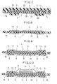
- FIGS. 13 to 16 are sectional views corresponding to FIGS. 3 to 5 for explaining another embodiment of the invention.
- the step of perforating the wiring board 1 having the copper foils 16 stuck on the front and back surfaces of the resin board 13 is effected first to provide the outer slits 15 for forming the resin sealing bodies 8 relative to the semiconductor integrated circuit chips to be mounted on the wiring board 1 .
- the step of perforating the wiring board 1 to provide the outer slits 15 may be effected at any step if this step is effected before the step of supplying the liquid sealing resin 18 to the semiconductor integrated circuit chips inside the outer slits 15 to form the resin sealing body 8 by heating and curing the liquid sealing resin 18 .
- cylindrical holes 11 a for providing the through holes on the wiring board 1 having the copper foils 16 on the front and back surfaces of the resin board 13 are provided by perforating means such as a cutting drill.
- a copper plating layer 17 a is formed by electroless plating treatment on the entire surface of the perforated resin board 13 including the inner peripheral surfaces of the cylindrical holes 11 a , thereby forming through holes 11 for electrically connecting the front and back surfaces of the wiring board 1 .
- the copper foil 16 provided on the resin board 13 and the copper plating layer 17 a formed by plating are integrated with each other, they are hereinafter referred to as a copper film 17 including the copper foil 16 .
- the wiring board 1 is perforated so as to provide substantially square outer slits 15 while leaving four corners thereof around an area where the semiconductor integrated circuit chips 2 are mounted on the wiring board 1 so as to form an outer shape of the resin sealing body for covering and protecting the semiconductor integrated circuit chips (see FIG. 2)
- a photoresist is applied onto the front and back surfaces of the wiring board 1 , then the photoresist on the front surface is patterned by applying thereto exposure and development treatments, so that an etching prevention film 20 made of the photoresist is formed on the front surface of the wiring board 1 , as shown in FIG. 16, only at the portion of the copper film 17 where the substrate electrodes 3 , the die pads 4 and the wiring patterns are formed.
- the etching prevention film 20 is also formed on the entire back surface of the wiring board 1 .
- the wiring board 1 is etched using an etchant so as to remove the copper film 17 at the portion which is not covered with the etching prevention film.
- substrate electrodes 3 , one die pad 4 and a wiring pattern are formed on the front surface of the resin board 13 in the same manner as shown in FIG. 6 of the first embodiment.
- the step of perforating the wiring board 1 to provide the outer slits 15 may be effected after the step of forming the copper films 17 by copper plating treatment.
- the step of perforating the wiring board 1 to provide the outer slits 15 may be effected after the step of patterning the copper films 17 on the front surface of the wiring board 1 to form the substrate electrodes 3 , the die pads 4 and so forth, or after the step of patterning the copper film 17 on the back surface of the wiring board 1 to form the pad electrodes or the like.
- the step of perforating the wiring board 1 to provide the outer slits 15 may be effected after the step of forming resin insulating films on the front and back surfaces of the wiring board 1 , or after the step of fixing the semiconductor integrated circuit chips 2 onto the die pad 4 on the front surface of the wiring board 1 by an adhesive or after the step of electrically connecting each electrode of the semiconductor integrated circuit chips 2 and each substrate electrode.
- the peripheral portions of the sealing body for protecting the semiconductor integrated circuit chips are curved in shape. Accordingly, the peripheral portions (particularly upper end edge portions) of the sealing body are not easily broken during the transportation of the semiconductor device. As a result, there does not arise a problem of a serious impairment of reliability of the semiconductor device caused by the breakage of the peripheral portions of the sealing body to produce cracks in the sealing body. Further, there does not arise a problem that the broken pieces produced by the breakage of the peripheral portions impede the functions of other electronic parts and parts conveying units.
- the method of fabricating the semiconductor device of the invention has a step of perforating the wiring board for providing the outer slits so as to form the sealing body to cover and protect the semiconductor integrated circuit chip while leaving four corners of the outer slits, the step of forming the sealing body inside the outer slits on every semiconductor integrated circuit chip, and the step of cutting the four corners of the outer slits where the wiring board is not perforated for providing the outer slits.
- volume of the cured sealing resin is not increased so that the shrinkage of volume of the cured sealing resin owing to the curing can be suppressed, and the wiring board is not warped.
Abstract
Description
Claims (2)
Applications Claiming Priority (2)
| Application Number | Priority Date | Filing Date | Title |
|---|---|---|---|
| JP11-122659 | 1999-04-28 | ||
| JP12265999 | 1999-04-28 |
Publications (1)
| Publication Number | Publication Date |
|---|---|
| US6329228B1 true US6329228B1 (en) | 2001-12-11 |
Family
ID=14841464
Family Applications (1)
| Application Number | Title | Priority Date | Filing Date |
|---|---|---|---|
| US09/559,311 Expired - Lifetime US6329228B1 (en) | 1999-04-28 | 2000-04-27 | Semiconductor device and method of fabricating the same |
Country Status (1)
| Country | Link |
|---|---|
| US (1) | US6329228B1 (en) |
Cited By (21)
| Publication number | Priority date | Publication date | Assignee | Title |
|---|---|---|---|---|
| US6548327B2 (en) * | 2000-04-24 | 2003-04-15 | Interuniversitair Microelektronica Centrum, Vzw | Low cost electroless plating process for single chips and wafer parts and products obtained thereof |
| US20030080439A1 (en) * | 2001-11-01 | 2003-05-01 | Siliconware Precision Industries Co., Ltd. | Delamination-preventing substrate and semiconductor package with the same |
| US6564452B2 (en) * | 1997-12-30 | 2003-05-20 | Intel Corporation | Method for creating printed circuit board substrates having solder mask-free edges |
| US6657294B2 (en) * | 2000-05-23 | 2003-12-02 | Koninklijke Philips Electronics N.V. | Data carrier having an IC module with a protection mechanism for protecting the parts of the IC module from mechanical stress |
| US6713864B1 (en) * | 2000-08-04 | 2004-03-30 | Siliconware Precision Industries Co., Ltd. | Semiconductor package for enhancing heat dissipation |
| US6790760B1 (en) * | 2000-07-21 | 2004-09-14 | Agere Systems Inc. | Method of manufacturing an integrated circuit package |
| US20060103004A1 (en) * | 2004-11-17 | 2006-05-18 | NEC CORPORATION and | Wiring board for semiconductor integrated circuit package and semiconductor integrated circuit device using the same |
| US20080036043A1 (en) * | 2004-11-25 | 2008-02-14 | Rohm Co., Ltd. | Manufacture Method for Semiconductor Device and Semiconductor Device |
| US20100015760A1 (en) * | 2001-06-07 | 2010-01-21 | Renesas Technology Corp. | Semiconductor device and manufacturing method thereof |
| US20110254150A1 (en) * | 2005-06-27 | 2011-10-20 | Texas Instruments Incorporated | Method of Manufacturing a Semiconductor Device |
| US20150123277A1 (en) * | 2010-09-22 | 2015-05-07 | Seiko Instruments Inc. | Ball grid array semiconductor package and method of manufacturing the same |
| USD729808S1 (en) | 2013-03-13 | 2015-05-19 | Nagrastar Llc | Smart card interface |
| USD758372S1 (en) * | 2013-03-13 | 2016-06-07 | Nagrastar Llc | Smart card interface |
| USD759022S1 (en) * | 2013-03-13 | 2016-06-14 | Nagrastar Llc | Smart card interface |
| USD780763S1 (en) | 2015-03-20 | 2017-03-07 | Nagrastar Llc | Smart card interface |
| US9647997B2 (en) | 2013-03-13 | 2017-05-09 | Nagrastar, Llc | USB interface for performing transport I/O |
| US9769521B2 (en) | 2013-03-13 | 2017-09-19 | Nagrastar, Llc | Systems and methods for performing transport I/O |
| US9814142B1 (en) * | 2015-06-24 | 2017-11-07 | Automated Assembly Corporation | Electronic devices wire bonded to substrate through an adhesive layer and method of making the same |
| US20180359860A1 (en) * | 2017-04-10 | 2018-12-13 | Tactotek Oy | Multilayer structure and related method of manufacture for electronics |
| USD864968S1 (en) | 2015-04-30 | 2019-10-29 | Echostar Technologies L.L.C. | Smart card interface |
| US11729915B1 (en) * | 2022-03-22 | 2023-08-15 | Tactotek Oy | Method for manufacturing a number of electrical nodes, electrical node module, electrical node, and multilayer structure |
Citations (3)
| Publication number | Priority date | Publication date | Assignee | Title |
|---|---|---|---|---|
| US5920117A (en) * | 1994-08-02 | 1999-07-06 | Fujitsu Limited | Semiconductor device and method of forming the device |
| US6074567A (en) * | 1997-02-12 | 2000-06-13 | Shinko Electric Industries Co., Ltd. | Method for producing a semiconductor package |
| US6157085A (en) * | 1998-04-07 | 2000-12-05 | Citizen Watch Co., Ltd. | Semiconductor device for preventing exfoliation from occurring between a semiconductor chip and a resin substrate |
-
2000
- 2000-04-27 US US09/559,311 patent/US6329228B1/en not_active Expired - Lifetime
Patent Citations (3)
| Publication number | Priority date | Publication date | Assignee | Title |
|---|---|---|---|---|
| US5920117A (en) * | 1994-08-02 | 1999-07-06 | Fujitsu Limited | Semiconductor device and method of forming the device |
| US6074567A (en) * | 1997-02-12 | 2000-06-13 | Shinko Electric Industries Co., Ltd. | Method for producing a semiconductor package |
| US6157085A (en) * | 1998-04-07 | 2000-12-05 | Citizen Watch Co., Ltd. | Semiconductor device for preventing exfoliation from occurring between a semiconductor chip and a resin substrate |
Cited By (42)
| Publication number | Priority date | Publication date | Assignee | Title |
|---|---|---|---|---|
| US6564452B2 (en) * | 1997-12-30 | 2003-05-20 | Intel Corporation | Method for creating printed circuit board substrates having solder mask-free edges |
| US6548327B2 (en) * | 2000-04-24 | 2003-04-15 | Interuniversitair Microelektronica Centrum, Vzw | Low cost electroless plating process for single chips and wafer parts and products obtained thereof |
| US6657294B2 (en) * | 2000-05-23 | 2003-12-02 | Koninklijke Philips Electronics N.V. | Data carrier having an IC module with a protection mechanism for protecting the parts of the IC module from mechanical stress |
| US6790760B1 (en) * | 2000-07-21 | 2004-09-14 | Agere Systems Inc. | Method of manufacturing an integrated circuit package |
| US6713864B1 (en) * | 2000-08-04 | 2004-03-30 | Siliconware Precision Industries Co., Ltd. | Semiconductor package for enhancing heat dissipation |
| US20100015760A1 (en) * | 2001-06-07 | 2010-01-21 | Renesas Technology Corp. | Semiconductor device and manufacturing method thereof |
| US8278147B2 (en) * | 2001-06-07 | 2012-10-02 | Renesas Electronics Corporation | Semiconductor device and manufacturing method thereof |
| US8952527B2 (en) | 2001-06-07 | 2015-02-10 | Renesas Electronics Corporation | Semiconductor device and manufacturing method thereof |
| US8653655B2 (en) | 2001-06-07 | 2014-02-18 | Renesas Electronics Corporation | Semiconductor device and manufacturing method thereof |
| US8524534B2 (en) | 2001-06-07 | 2013-09-03 | Renesas Electronics Corporation | Semiconductor device and manufacturing method thereof |
| US9613922B2 (en) | 2001-06-07 | 2017-04-04 | Renesas Electronics Corporation | Semiconductor device and manufacturing method thereof |
| US20110171780A1 (en) * | 2001-06-07 | 2011-07-14 | Renesas Electronics Corporation | Semiconductor device and manufacturing method thereof |
| US6608388B2 (en) * | 2001-11-01 | 2003-08-19 | Siliconware Precision Industries Co., Ltd. | Delamination-preventing substrate and semiconductor package with the same |
| US20030080439A1 (en) * | 2001-11-01 | 2003-05-01 | Siliconware Precision Industries Co., Ltd. | Delamination-preventing substrate and semiconductor package with the same |
| US7321166B2 (en) * | 2004-11-17 | 2008-01-22 | Nec Corporation | Wiring board having connecting wiring between electrode plane and connecting pad |
| US20060103004A1 (en) * | 2004-11-17 | 2006-05-18 | NEC CORPORATION and | Wiring board for semiconductor integrated circuit package and semiconductor integrated circuit device using the same |
| US7928581B2 (en) * | 2004-11-25 | 2011-04-19 | Rohm Co., Ltd. | Semiconductor device having a conductive member including an end face substantially fush with an end face of a wiring board and method of manufacturing the same |
| US20080036043A1 (en) * | 2004-11-25 | 2008-02-14 | Rohm Co., Ltd. | Manufacture Method for Semiconductor Device and Semiconductor Device |
| US20110254150A1 (en) * | 2005-06-27 | 2011-10-20 | Texas Instruments Incorporated | Method of Manufacturing a Semiconductor Device |
| US8304883B2 (en) * | 2005-06-27 | 2012-11-06 | Texas Instruments Incorporated | Semiconductor device having multiple semiconductor elements |
| US20150123277A1 (en) * | 2010-09-22 | 2015-05-07 | Seiko Instruments Inc. | Ball grid array semiconductor package and method of manufacturing the same |
| US9245864B2 (en) * | 2010-09-22 | 2016-01-26 | Seiko Instruments Inc. | Ball grid array semiconductor package and method of manufacturing the same |
| USD729808S1 (en) | 2013-03-13 | 2015-05-19 | Nagrastar Llc | Smart card interface |
| US9774908B2 (en) | 2013-03-13 | 2017-09-26 | Nagrastar, Llc | Systems and methods for performing transport I/O |
| USD780184S1 (en) | 2013-03-13 | 2017-02-28 | Nagrastar Llc | Smart card interface |
| USD949864S1 (en) * | 2013-03-13 | 2022-04-26 | Nagrastar Llc | Smart card interface |
| USD758372S1 (en) * | 2013-03-13 | 2016-06-07 | Nagrastar Llc | Smart card interface |
| US9647997B2 (en) | 2013-03-13 | 2017-05-09 | Nagrastar, Llc | USB interface for performing transport I/O |
| USD792411S1 (en) | 2013-03-13 | 2017-07-18 | Nagrastar Llc | Smart card interface |
| USD792410S1 (en) | 2013-03-13 | 2017-07-18 | Nagrastar Llc | Smart card interface |
| US9769521B2 (en) | 2013-03-13 | 2017-09-19 | Nagrastar, Llc | Systems and methods for performing transport I/O |
| USD759022S1 (en) * | 2013-03-13 | 2016-06-14 | Nagrastar Llc | Smart card interface |
| US10382816B2 (en) | 2013-03-13 | 2019-08-13 | Nagrastar, Llc | Systems and methods for performing transport I/O |
| US9888283B2 (en) | 2013-03-13 | 2018-02-06 | Nagrastar Llc | Systems and methods for performing transport I/O |
| US10070176B2 (en) | 2013-03-13 | 2018-09-04 | Nagrastar, Llc | Systems and methods for performing transport I/O |
| USD840404S1 (en) | 2013-03-13 | 2019-02-12 | Nagrastar, Llc | Smart card interface |
| USD780763S1 (en) | 2015-03-20 | 2017-03-07 | Nagrastar Llc | Smart card interface |
| USD864968S1 (en) | 2015-04-30 | 2019-10-29 | Echostar Technologies L.L.C. | Smart card interface |
| US9814142B1 (en) * | 2015-06-24 | 2017-11-07 | Automated Assembly Corporation | Electronic devices wire bonded to substrate through an adhesive layer and method of making the same |
| US20180359860A1 (en) * | 2017-04-10 | 2018-12-13 | Tactotek Oy | Multilayer structure and related method of manufacture for electronics |
| US10667401B2 (en) * | 2017-04-10 | 2020-05-26 | Tactotek Oy | Multilayer structure and related method of manufacture for electronics |
| US11729915B1 (en) * | 2022-03-22 | 2023-08-15 | Tactotek Oy | Method for manufacturing a number of electrical nodes, electrical node module, electrical node, and multilayer structure |
Similar Documents
| Publication | Publication Date | Title |
|---|---|---|
| US6329228B1 (en) | Semiconductor device and method of fabricating the same | |
| RU2146067C1 (en) | Organic chip holder for integrated circuits with wire connections | |
| US6534391B1 (en) | Semiconductor package having substrate with laser-formed aperture through solder mask layer | |
| US6586274B2 (en) | Semiconductor device, substrate for a semiconductor device, method of manufacture thereof, and electronic instrument | |
| JP3578770B2 (en) | Semiconductor device | |
| US6794739B2 (en) | Semiconductor device, process for production thereof, and electronic equipment | |
| US6020629A (en) | Stacked semiconductor package and method of fabrication | |
| US6909178B2 (en) | Semiconductor device and method of manufacturing the same | |
| US9949372B2 (en) | Printed wiring board and method for manufacturing the same | |
| TW200941659A (en) | Thermally enhanced package with embedded metal slug and patterned circuitry | |
| US7923835B2 (en) | Package, electronic device, substrate having a separation region and a wiring layers, and method for manufacturing | |
| US6558981B2 (en) | Method for making an encapsulated semiconductor chip module | |
| US6175152B1 (en) | Semiconductor device | |
| US20090184413A1 (en) | Insulative wiring board, semiconductor package using the same, and method for producing the insulative wiring board | |
| JP3691335B2 (en) | Circuit device manufacturing method | |
| CN111199924A (en) | Semiconductor packaging structure and manufacturing method thereof | |
| JPH0864635A (en) | Semiconductor device | |
| JPH104151A (en) | Semiconductor device and its manufacture | |
| JP4321758B2 (en) | Semiconductor device | |
| JP2936540B2 (en) | Circuit board, method of manufacturing the same, and method of manufacturing semiconductor package using the same | |
| JPH0897330A (en) | Chip carrier and manufacture thereof | |
| JP3684517B2 (en) | Semiconductor device | |
| KR100537835B1 (en) | Semiconductor package and method for manufacturing the same | |
| JPH08102583A (en) | Wiring circuit substrate | |
| JP2000031195A (en) | Semiconductor device and production thereof |
Legal Events
| Date | Code | Title | Description |
|---|---|---|---|
| AS | Assignment |
Owner name: CITIZEN WATCH CO. LTD., JAPAN Free format text: ASSIGNMENT OF ASSIGNORS INTEREST;ASSIGNOR:TERASHIMA, KAZUHIKO;REEL/FRAME:011080/0764 Effective date: 20000905 |
|
| AS | Assignment |
Owner name: CITIZEN WATCH CO., LTD., JAPAN Free format text: CHANGE OF ASSIGNEE'S ADDRESS;ASSIGNOR:CITIZEN WATCH CO., LTD.;REEL/FRAME:011995/0591 Effective date: 20010301 |
|
| STCF | Information on status: patent grant |
Free format text: PATENTED CASE |
|
| FPAY | Fee payment |
Year of fee payment: 4 |
|
| AS | Assignment |
Owner name: CITIZEN HOLDINGS CO., LTD., JAPAN Free format text: CHANGE OF NAME;ASSIGNOR:CITIZEN WATCH CO., LTD.;REEL/FRAME:019817/0701 Effective date: 20070402 |
|
| FEPP | Fee payment procedure |
Free format text: PAYOR NUMBER ASSIGNED (ORIGINAL EVENT CODE: ASPN); ENTITY STATUS OF PATENT OWNER: LARGE ENTITY |
|
| FPAY | Fee payment |
Year of fee payment: 8 |
|
| FPAY | Fee payment |
Year of fee payment: 12 |
|
| AS | Assignment |
Owner name: CITIZEN WATCH CO., LTD., JAPAN Free format text: CHANGE OF NAME;ASSIGNOR:CITIZEN HOLDINGS CO., LTD.;REEL/FRAME:041479/0804 Effective date: 20161005 |