WO2015137373A1 - Semiconductor device - Google Patents
Semiconductor device Download PDFInfo
- Publication number
- WO2015137373A1 WO2015137373A1 PCT/JP2015/057093 JP2015057093W WO2015137373A1 WO 2015137373 A1 WO2015137373 A1 WO 2015137373A1 JP 2015057093 W JP2015057093 W JP 2015057093W WO 2015137373 A1 WO2015137373 A1 WO 2015137373A1
- Authority
- WO
- WIPO (PCT)
- Prior art keywords
- layer
- semiconductor
- concentration
- active layer
- type
- Prior art date
Links
- 239000004065 semiconductor Substances 0.000 title claims abstract description 282
- 229910052757 nitrogen Inorganic materials 0.000 claims abstract description 34
- 229910052698 phosphorus Inorganic materials 0.000 claims abstract description 34
- 229910021478 group 5 element Inorganic materials 0.000 claims abstract description 27
- 229910052787 antimony Inorganic materials 0.000 claims abstract description 23
- 229910001218 Gallium arsenide Inorganic materials 0.000 claims description 78
- 239000013078 crystal Substances 0.000 claims description 66
- 230000004888 barrier function Effects 0.000 claims description 40
- 239000002019 doping agent Substances 0.000 claims description 31
- 229910000530 Gallium indium arsenide Inorganic materials 0.000 claims description 17
- 229910000980 Aluminium gallium arsenide Inorganic materials 0.000 claims description 15
- 230000007547 defect Effects 0.000 abstract description 9
- 125000004429 atom Chemical group 0.000 description 102
- JBRZTFJDHDCESZ-UHFFFAOYSA-N AsGa Chemical compound [As]#[Ga] JBRZTFJDHDCESZ-UHFFFAOYSA-N 0.000 description 76
- 230000015572 biosynthetic process Effects 0.000 description 68
- 230000000694 effects Effects 0.000 description 49
- 239000012535 impurity Substances 0.000 description 42
- 239000000758 substrate Substances 0.000 description 30
- 238000009792 diffusion process Methods 0.000 description 27
- MDPILPRLPQYEEN-UHFFFAOYSA-N aluminium arsenide Chemical compound [As]#[Al] MDPILPRLPQYEEN-UHFFFAOYSA-N 0.000 description 23
- 238000000034 method Methods 0.000 description 20
- 239000000203 mixture Substances 0.000 description 19
- 230000006866 deterioration Effects 0.000 description 16
- 239000002244 precipitate Substances 0.000 description 16
- 230000007423 decrease Effects 0.000 description 15
- 229910052738 indium Inorganic materials 0.000 description 14
- 238000005259 measurement Methods 0.000 description 13
- 239000000523 sample Substances 0.000 description 13
- 238000004364 calculation method Methods 0.000 description 12
- 230000002829 reductive effect Effects 0.000 description 12
- 230000010355 oscillation Effects 0.000 description 11
- 229910052733 gallium Inorganic materials 0.000 description 9
- 230000003287 optical effect Effects 0.000 description 9
- 230000005855 radiation Effects 0.000 description 9
- 238000012795 verification Methods 0.000 description 9
- 229910052782 aluminium Inorganic materials 0.000 description 7
- 238000010586 diagram Methods 0.000 description 7
- 150000002500 ions Chemical class 0.000 description 7
- 230000007935 neutral effect Effects 0.000 description 7
- 230000036961 partial effect Effects 0.000 description 7
- 238000001004 secondary ion mass spectrometry Methods 0.000 description 7
- 238000004088 simulation Methods 0.000 description 7
- 230000005684 electric field Effects 0.000 description 6
- 238000002474 experimental method Methods 0.000 description 6
- 230000007246 mechanism Effects 0.000 description 6
- 239000011159 matrix material Substances 0.000 description 5
- 239000011669 selenium Substances 0.000 description 5
- IJGRMHOSHXDMSA-UHFFFAOYSA-N Atomic nitrogen Chemical compound N#N IJGRMHOSHXDMSA-UHFFFAOYSA-N 0.000 description 4
- 239000000969 carrier Substances 0.000 description 4
- 230000008859 change Effects 0.000 description 4
- 238000001514 detection method Methods 0.000 description 4
- 230000004048 modification Effects 0.000 description 4
- 238000012986 modification Methods 0.000 description 4
- 125000004437 phosphorous atom Chemical group 0.000 description 4
- 230000002040 relaxant effect Effects 0.000 description 4
- 230000035945 sensitivity Effects 0.000 description 4
- 238000001069 Raman spectroscopy Methods 0.000 description 3
- 230000001133 acceleration Effects 0.000 description 3
- 239000002131 composite material Substances 0.000 description 3
- 238000005468 ion implantation Methods 0.000 description 3
- 230000007774 longterm Effects 0.000 description 3
- 229920002120 photoresistant polymer Polymers 0.000 description 3
- 229910052711 selenium Inorganic materials 0.000 description 3
- 230000006641 stabilisation Effects 0.000 description 3
- 238000011105 stabilization Methods 0.000 description 3
- 230000000087 stabilizing effect Effects 0.000 description 3
- 239000000126 substance Substances 0.000 description 3
- XEEYBQQBJWHFJM-UHFFFAOYSA-N Iron Chemical compound [Fe] XEEYBQQBJWHFJM-UHFFFAOYSA-N 0.000 description 2
- NBIIXXVUZAFLBC-UHFFFAOYSA-N Phosphoric acid Chemical compound OP(O)(O)=O NBIIXXVUZAFLBC-UHFFFAOYSA-N 0.000 description 2
- BUGBHKTXTAQXES-UHFFFAOYSA-N Selenium Chemical compound [Se] BUGBHKTXTAQXES-UHFFFAOYSA-N 0.000 description 2
- XUIMIQQOPSSXEZ-UHFFFAOYSA-N Silicon Chemical compound [Si] XUIMIQQOPSSXEZ-UHFFFAOYSA-N 0.000 description 2
- 238000002441 X-ray diffraction Methods 0.000 description 2
- 239000000370 acceptor Substances 0.000 description 2
- 230000002411 adverse Effects 0.000 description 2
- 229910045601 alloy Inorganic materials 0.000 description 2
- 239000000956 alloy Substances 0.000 description 2
- 229910052785 arsenic Inorganic materials 0.000 description 2
- RQNWIZPPADIBDY-UHFFFAOYSA-N arsenic atom Chemical compound [As] RQNWIZPPADIBDY-UHFFFAOYSA-N 0.000 description 2
- 230000005540 biological transmission Effects 0.000 description 2
- 230000015556 catabolic process Effects 0.000 description 2
- 230000006378 damage Effects 0.000 description 2
- 238000009826 distribution Methods 0.000 description 2
- 238000005516 engineering process Methods 0.000 description 2
- 238000005530 etching Methods 0.000 description 2
- 238000011156 evaluation Methods 0.000 description 2
- 238000010438 heat treatment Methods 0.000 description 2
- 238000000691 measurement method Methods 0.000 description 2
- 238000001451 molecular beam epitaxy Methods 0.000 description 2
- 230000006911 nucleation Effects 0.000 description 2
- 238000010899 nucleation Methods 0.000 description 2
- 230000008569 process Effects 0.000 description 2
- 238000004574 scanning tunneling microscopy Methods 0.000 description 2
- 229910052710 silicon Inorganic materials 0.000 description 2
- 239000010703 silicon Substances 0.000 description 2
- 239000007787 solid Substances 0.000 description 2
- 229910052717 sulfur Inorganic materials 0.000 description 2
- 230000001629 suppression Effects 0.000 description 2
- 230000002195 synergetic effect Effects 0.000 description 2
- 230000005533 two-dimensional electron gas Effects 0.000 description 2
- OKTJSMMVPCPJKN-UHFFFAOYSA-N Carbon Chemical compound [C] OKTJSMMVPCPJKN-UHFFFAOYSA-N 0.000 description 1
- GYHNNYVSQQEPJS-UHFFFAOYSA-N Gallium Chemical group [Ga] GYHNNYVSQQEPJS-UHFFFAOYSA-N 0.000 description 1
- 206010053759 Growth retardation Diseases 0.000 description 1
- MHAJPDPJQMAIIY-UHFFFAOYSA-N Hydrogen peroxide Chemical compound OO MHAJPDPJQMAIIY-UHFFFAOYSA-N 0.000 description 1
- 229910000673 Indium arsenide Inorganic materials 0.000 description 1
- OAICVXFJPJFONN-UHFFFAOYSA-N Phosphorus Chemical compound [P] OAICVXFJPJFONN-UHFFFAOYSA-N 0.000 description 1
- KJTLSVCANCCWHF-UHFFFAOYSA-N Ruthenium Chemical compound [Ru] KJTLSVCANCCWHF-UHFFFAOYSA-N 0.000 description 1
- 229910004298 SiO 2 Inorganic materials 0.000 description 1
- NINIDFKCEFEMDL-UHFFFAOYSA-N Sulfur Chemical compound [S] NINIDFKCEFEMDL-UHFFFAOYSA-N 0.000 description 1
- 238000010521 absorption reaction Methods 0.000 description 1
- 229910000147 aluminium phosphate Inorganic materials 0.000 description 1
- 238000004458 analytical method Methods 0.000 description 1
- WATWJIUSRGPENY-UHFFFAOYSA-N antimony atom Chemical compound [Sb] WATWJIUSRGPENY-UHFFFAOYSA-N 0.000 description 1
- 230000008901 benefit Effects 0.000 description 1
- 229910052799 carbon Inorganic materials 0.000 description 1
- 238000005253 cladding Methods 0.000 description 1
- 239000000470 constituent Substances 0.000 description 1
- 238000002425 crystallisation Methods 0.000 description 1
- 230000008025 crystallization Effects 0.000 description 1
- 238000000354 decomposition reaction Methods 0.000 description 1
- 230000003247 decreasing effect Effects 0.000 description 1
- 238000013461 design Methods 0.000 description 1
- 230000007613 environmental effect Effects 0.000 description 1
- 230000008020 evaporation Effects 0.000 description 1
- 238000001704 evaporation Methods 0.000 description 1
- 239000007789 gas Substances 0.000 description 1
- QOSATHPSBFQAML-UHFFFAOYSA-N hydrogen peroxide;hydrate Chemical compound O.OO QOSATHPSBFQAML-UHFFFAOYSA-N 0.000 description 1
- RPQDHPTXJYYUPQ-UHFFFAOYSA-N indium arsenide Chemical compound [In]#[As] RPQDHPTXJYYUPQ-UHFFFAOYSA-N 0.000 description 1
- APFVFJFRJDLVQX-UHFFFAOYSA-N indium atom Chemical compound [In] APFVFJFRJDLVQX-UHFFFAOYSA-N 0.000 description 1
- 230000010354 integration Effects 0.000 description 1
- 230000003993 interaction Effects 0.000 description 1
- 238000010884 ion-beam technique Methods 0.000 description 1
- 239000007788 liquid Substances 0.000 description 1
- 238000004519 manufacturing process Methods 0.000 description 1
- 239000000463 material Substances 0.000 description 1
- 229910052751 metal Inorganic materials 0.000 description 1
- 239000002184 metal Substances 0.000 description 1
- 238000002488 metal-organic chemical vapour deposition Methods 0.000 description 1
- 239000011259 mixed solution Substances 0.000 description 1
- 230000001590 oxidative effect Effects 0.000 description 1
- 230000002093 peripheral effect Effects 0.000 description 1
- 239000011574 phosphorus Substances 0.000 description 1
- 238000000206 photolithography Methods 0.000 description 1
- 238000005424 photoluminescence Methods 0.000 description 1
- 230000010287 polarization Effects 0.000 description 1
- 238000002360 preparation method Methods 0.000 description 1
- 238000012545 processing Methods 0.000 description 1
- 238000011002 quantification Methods 0.000 description 1
- 239000013074 reference sample Substances 0.000 description 1
- 230000004044 response Effects 0.000 description 1
- 230000002441 reversible effect Effects 0.000 description 1
- 230000000630 rising effect Effects 0.000 description 1
- 229910052707 ruthenium Inorganic materials 0.000 description 1
- WGPCGCOKHWGKJJ-UHFFFAOYSA-N sulfanylidenezinc Chemical compound [Zn]=S WGPCGCOKHWGKJJ-UHFFFAOYSA-N 0.000 description 1
- 239000011593 sulfur Substances 0.000 description 1
- 238000004441 surface measurement Methods 0.000 description 1
- 230000005641 tunneling Effects 0.000 description 1
- XLYOFNOQVPJJNP-UHFFFAOYSA-N water Substances O XLYOFNOQVPJJNP-UHFFFAOYSA-N 0.000 description 1
- 230000005428 wave function Effects 0.000 description 1
- 238000001039 wet etching Methods 0.000 description 1
- 229910052984 zinc sulfide Inorganic materials 0.000 description 1
Images


Classifications
-
- H—ELECTRICITY
- H01—ELECTRIC ELEMENTS
- H01S—DEVICES USING THE PROCESS OF LIGHT AMPLIFICATION BY STIMULATED EMISSION OF RADIATION [LASER] TO AMPLIFY OR GENERATE LIGHT; DEVICES USING STIMULATED EMISSION OF ELECTROMAGNETIC RADIATION IN WAVE RANGES OTHER THAN OPTICAL
- H01S5/00—Semiconductor lasers
- H01S5/30—Structure or shape of the active region; Materials used for the active region
- H01S5/34—Structure or shape of the active region; Materials used for the active region comprising quantum well or superlattice structures, e.g. single quantum well [SQW] lasers, multiple quantum well [MQW] lasers or graded index separate confinement heterostructure [GRINSCH] lasers
- H01S5/343—Structure or shape of the active region; Materials used for the active region comprising quantum well or superlattice structures, e.g. single quantum well [SQW] lasers, multiple quantum well [MQW] lasers or graded index separate confinement heterostructure [GRINSCH] lasers in AIIIBV compounds, e.g. AlGaAs-laser, InP-based laser
- H01S5/34313—Structure or shape of the active region; Materials used for the active region comprising quantum well or superlattice structures, e.g. single quantum well [SQW] lasers, multiple quantum well [MQW] lasers or graded index separate confinement heterostructure [GRINSCH] lasers in AIIIBV compounds, e.g. AlGaAs-laser, InP-based laser with a well layer having only As as V-compound, e.g. AlGaAs, InGaAs
-
- H—ELECTRICITY
- H01—ELECTRIC ELEMENTS
- H01L—SEMICONDUCTOR DEVICES NOT COVERED BY CLASS H10
- H01L21/00—Processes or apparatus adapted for the manufacture or treatment of semiconductor or solid state devices or of parts thereof
- H01L21/02—Manufacture or treatment of semiconductor devices or of parts thereof
- H01L21/02104—Forming layers
- H01L21/02365—Forming inorganic semiconducting materials on a substrate
- H01L21/02518—Deposited layers
- H01L21/0257—Doping during depositing
- H01L21/02573—Conductivity type
- H01L21/02576—N-type
-
- H—ELECTRICITY
- H01—ELECTRIC ELEMENTS
- H01L—SEMICONDUCTOR DEVICES NOT COVERED BY CLASS H10
- H01L29/00—Semiconductor devices adapted for rectifying, amplifying, oscillating or switching, or capacitors or resistors with at least one potential-jump barrier or surface barrier, e.g. PN junction depletion layer or carrier concentration layer; Details of semiconductor bodies or of electrodes thereof ; Multistep manufacturing processes therefor
- H01L29/02—Semiconductor bodies ; Multistep manufacturing processes therefor
- H01L29/04—Semiconductor bodies ; Multistep manufacturing processes therefor characterised by their crystalline structure, e.g. polycrystalline, cubic or particular orientation of crystalline planes
- H01L29/045—Semiconductor bodies ; Multistep manufacturing processes therefor characterised by their crystalline structure, e.g. polycrystalline, cubic or particular orientation of crystalline planes by their particular orientation of crystalline planes
-
- H—ELECTRICITY
- H01—ELECTRIC ELEMENTS
- H01L—SEMICONDUCTOR DEVICES NOT COVERED BY CLASS H10
- H01L29/00—Semiconductor devices adapted for rectifying, amplifying, oscillating or switching, or capacitors or resistors with at least one potential-jump barrier or surface barrier, e.g. PN junction depletion layer or carrier concentration layer; Details of semiconductor bodies or of electrodes thereof ; Multistep manufacturing processes therefor
- H01L29/02—Semiconductor bodies ; Multistep manufacturing processes therefor
- H01L29/12—Semiconductor bodies ; Multistep manufacturing processes therefor characterised by the materials of which they are formed
- H01L29/20—Semiconductor bodies ; Multistep manufacturing processes therefor characterised by the materials of which they are formed including, apart from doping materials or other impurities, only AIIIBV compounds
- H01L29/201—Semiconductor bodies ; Multistep manufacturing processes therefor characterised by the materials of which they are formed including, apart from doping materials or other impurities, only AIIIBV compounds including two or more compounds, e.g. alloys
- H01L29/205—Semiconductor bodies ; Multistep manufacturing processes therefor characterised by the materials of which they are formed including, apart from doping materials or other impurities, only AIIIBV compounds including two or more compounds, e.g. alloys in different semiconductor regions, e.g. heterojunctions
-
- H—ELECTRICITY
- H01—ELECTRIC ELEMENTS
- H01L—SEMICONDUCTOR DEVICES NOT COVERED BY CLASS H10
- H01L29/00—Semiconductor devices adapted for rectifying, amplifying, oscillating or switching, or capacitors or resistors with at least one potential-jump barrier or surface barrier, e.g. PN junction depletion layer or carrier concentration layer; Details of semiconductor bodies or of electrodes thereof ; Multistep manufacturing processes therefor
- H01L29/66—Types of semiconductor device ; Multistep manufacturing processes therefor
- H01L29/68—Types of semiconductor device ; Multistep manufacturing processes therefor controllable by only the electric current supplied, or only the electric potential applied, to an electrode which does not carry the current to be rectified, amplified or switched
- H01L29/76—Unipolar devices, e.g. field effect transistors
- H01L29/772—Field effect transistors
- H01L29/778—Field effect transistors with two-dimensional charge carrier gas channel, e.g. HEMT ; with two-dimensional charge-carrier layer formed at a heterojunction interface
- H01L29/7782—Field effect transistors with two-dimensional charge carrier gas channel, e.g. HEMT ; with two-dimensional charge-carrier layer formed at a heterojunction interface with confinement of carriers by at least two heterojunctions, e.g. DHHEMT, quantum well HEMT, DHMODFET
- H01L29/7783—Field effect transistors with two-dimensional charge carrier gas channel, e.g. HEMT ; with two-dimensional charge-carrier layer formed at a heterojunction interface with confinement of carriers by at least two heterojunctions, e.g. DHHEMT, quantum well HEMT, DHMODFET using III-V semiconductor material
- H01L29/7784—Field effect transistors with two-dimensional charge carrier gas channel, e.g. HEMT ; with two-dimensional charge-carrier layer formed at a heterojunction interface with confinement of carriers by at least two heterojunctions, e.g. DHHEMT, quantum well HEMT, DHMODFET using III-V semiconductor material with delta or planar doped donor layer
-
- H—ELECTRICITY
- H01—ELECTRIC ELEMENTS
- H01L—SEMICONDUCTOR DEVICES NOT COVERED BY CLASS H10
- H01L29/00—Semiconductor devices adapted for rectifying, amplifying, oscillating or switching, or capacitors or resistors with at least one potential-jump barrier or surface barrier, e.g. PN junction depletion layer or carrier concentration layer; Details of semiconductor bodies or of electrodes thereof ; Multistep manufacturing processes therefor
- H01L29/66—Types of semiconductor device ; Multistep manufacturing processes therefor
- H01L29/68—Types of semiconductor device ; Multistep manufacturing processes therefor controllable by only the electric current supplied, or only the electric potential applied, to an electrode which does not carry the current to be rectified, amplified or switched
- H01L29/76—Unipolar devices, e.g. field effect transistors
- H01L29/772—Field effect transistors
- H01L29/778—Field effect transistors with two-dimensional charge carrier gas channel, e.g. HEMT ; with two-dimensional charge-carrier layer formed at a heterojunction interface
- H01L29/7786—Field effect transistors with two-dimensional charge carrier gas channel, e.g. HEMT ; with two-dimensional charge-carrier layer formed at a heterojunction interface with direct single heterostructure, i.e. with wide bandgap layer formed on top of active layer, e.g. direct single heterostructure MIS-like HEMT
- H01L29/7787—Field effect transistors with two-dimensional charge carrier gas channel, e.g. HEMT ; with two-dimensional charge-carrier layer formed at a heterojunction interface with direct single heterostructure, i.e. with wide bandgap layer formed on top of active layer, e.g. direct single heterostructure MIS-like HEMT with wide bandgap charge-carrier supplying layer, e.g. direct single heterostructure MODFET
-
- H—ELECTRICITY
- H01—ELECTRIC ELEMENTS
- H01L—SEMICONDUCTOR DEVICES NOT COVERED BY CLASS H10
- H01L29/00—Semiconductor devices adapted for rectifying, amplifying, oscillating or switching, or capacitors or resistors with at least one potential-jump barrier or surface barrier, e.g. PN junction depletion layer or carrier concentration layer; Details of semiconductor bodies or of electrodes thereof ; Multistep manufacturing processes therefor
- H01L29/66—Types of semiconductor device ; Multistep manufacturing processes therefor
- H01L29/86—Types of semiconductor device ; Multistep manufacturing processes therefor controllable only by variation of the electric current supplied, or only the electric potential applied, to one or more of the electrodes carrying the current to be rectified, amplified, oscillated or switched
- H01L29/861—Diodes
- H01L29/868—PIN diodes
-
- H—ELECTRICITY
- H01—ELECTRIC ELEMENTS
- H01L—SEMICONDUCTOR DEVICES NOT COVERED BY CLASS H10
- H01L31/00—Semiconductor devices sensitive to infrared radiation, light, electromagnetic radiation of shorter wavelength or corpuscular radiation and specially adapted either for the conversion of the energy of such radiation into electrical energy or for the control of electrical energy by such radiation; Processes or apparatus specially adapted for the manufacture or treatment thereof or of parts thereof; Details thereof
- H01L31/0248—Semiconductor devices sensitive to infrared radiation, light, electromagnetic radiation of shorter wavelength or corpuscular radiation and specially adapted either for the conversion of the energy of such radiation into electrical energy or for the control of electrical energy by such radiation; Processes or apparatus specially adapted for the manufacture or treatment thereof or of parts thereof; Details thereof characterised by their semiconductor bodies
- H01L31/0256—Semiconductor devices sensitive to infrared radiation, light, electromagnetic radiation of shorter wavelength or corpuscular radiation and specially adapted either for the conversion of the energy of such radiation into electrical energy or for the control of electrical energy by such radiation; Processes or apparatus specially adapted for the manufacture or treatment thereof or of parts thereof; Details thereof characterised by their semiconductor bodies characterised by the material
- H01L31/0264—Inorganic materials
- H01L31/0304—Inorganic materials including, apart from doping materials or other impurities, only AIIIBV compounds
- H01L31/03046—Inorganic materials including, apart from doping materials or other impurities, only AIIIBV compounds including ternary or quaternary compounds, e.g. GaAlAs, InGaAs, InGaAsP
-
- H—ELECTRICITY
- H01—ELECTRIC ELEMENTS
- H01L—SEMICONDUCTOR DEVICES NOT COVERED BY CLASS H10
- H01L31/00—Semiconductor devices sensitive to infrared radiation, light, electromagnetic radiation of shorter wavelength or corpuscular radiation and specially adapted either for the conversion of the energy of such radiation into electrical energy or for the control of electrical energy by such radiation; Processes or apparatus specially adapted for the manufacture or treatment thereof or of parts thereof; Details thereof
- H01L31/0248—Semiconductor devices sensitive to infrared radiation, light, electromagnetic radiation of shorter wavelength or corpuscular radiation and specially adapted either for the conversion of the energy of such radiation into electrical energy or for the control of electrical energy by such radiation; Processes or apparatus specially adapted for the manufacture or treatment thereof or of parts thereof; Details thereof characterised by their semiconductor bodies
- H01L31/036—Semiconductor devices sensitive to infrared radiation, light, electromagnetic radiation of shorter wavelength or corpuscular radiation and specially adapted either for the conversion of the energy of such radiation into electrical energy or for the control of electrical energy by such radiation; Processes or apparatus specially adapted for the manufacture or treatment thereof or of parts thereof; Details thereof characterised by their semiconductor bodies characterised by their crystalline structure or particular orientation of the crystalline planes
-
- H—ELECTRICITY
- H01—ELECTRIC ELEMENTS
- H01L—SEMICONDUCTOR DEVICES NOT COVERED BY CLASS H10
- H01L31/00—Semiconductor devices sensitive to infrared radiation, light, electromagnetic radiation of shorter wavelength or corpuscular radiation and specially adapted either for the conversion of the energy of such radiation into electrical energy or for the control of electrical energy by such radiation; Processes or apparatus specially adapted for the manufacture or treatment thereof or of parts thereof; Details thereof
- H01L31/08—Semiconductor devices sensitive to infrared radiation, light, electromagnetic radiation of shorter wavelength or corpuscular radiation and specially adapted either for the conversion of the energy of such radiation into electrical energy or for the control of electrical energy by such radiation; Processes or apparatus specially adapted for the manufacture or treatment thereof or of parts thereof; Details thereof in which radiation controls flow of current through the device, e.g. photoresistors
- H01L31/10—Semiconductor devices sensitive to infrared radiation, light, electromagnetic radiation of shorter wavelength or corpuscular radiation and specially adapted either for the conversion of the energy of such radiation into electrical energy or for the control of electrical energy by such radiation; Processes or apparatus specially adapted for the manufacture or treatment thereof or of parts thereof; Details thereof in which radiation controls flow of current through the device, e.g. photoresistors characterised by at least one potential-jump barrier or surface barrier, e.g. phototransistors
- H01L31/101—Devices sensitive to infrared, visible or ultraviolet radiation
- H01L31/102—Devices sensitive to infrared, visible or ultraviolet radiation characterised by only one potential barrier or surface barrier
- H01L31/105—Devices sensitive to infrared, visible or ultraviolet radiation characterised by only one potential barrier or surface barrier the potential barrier being of the PIN type
-
- H—ELECTRICITY
- H01—ELECTRIC ELEMENTS
- H01S—DEVICES USING THE PROCESS OF LIGHT AMPLIFICATION BY STIMULATED EMISSION OF RADIATION [LASER] TO AMPLIFY OR GENERATE LIGHT; DEVICES USING STIMULATED EMISSION OF ELECTROMAGNETIC RADIATION IN WAVE RANGES OTHER THAN OPTICAL
- H01S5/00—Semiconductor lasers
- H01S5/20—Structure or shape of the semiconductor body to guide the optical wave ; Confining structures perpendicular to the optical axis, e.g. index or gain guiding, stripe geometry, broad area lasers, gain tailoring, transverse or lateral reflectors, special cladding structures, MQW barrier reflection layers
- H01S5/22—Structure or shape of the semiconductor body to guide the optical wave ; Confining structures perpendicular to the optical axis, e.g. index or gain guiding, stripe geometry, broad area lasers, gain tailoring, transverse or lateral reflectors, special cladding structures, MQW barrier reflection layers having a ridge or stripe structure
- H01S5/227—Buried mesa structure ; Striped active layer
-
- H—ELECTRICITY
- H01—ELECTRIC ELEMENTS
- H01S—DEVICES USING THE PROCESS OF LIGHT AMPLIFICATION BY STIMULATED EMISSION OF RADIATION [LASER] TO AMPLIFY OR GENERATE LIGHT; DEVICES USING STIMULATED EMISSION OF ELECTROMAGNETIC RADIATION IN WAVE RANGES OTHER THAN OPTICAL
- H01S5/00—Semiconductor lasers
- H01S5/30—Structure or shape of the active region; Materials used for the active region
- H01S5/305—Structure or shape of the active region; Materials used for the active region characterised by the doping materials used in the laser structure
- H01S5/3086—Structure or shape of the active region; Materials used for the active region characterised by the doping materials used in the laser structure doping of the active layer
- H01S5/309—Structure or shape of the active region; Materials used for the active region characterised by the doping materials used in the laser structure doping of the active layer doping of barrier layers that confine charge carriers in the laser structure, e.g. the barriers in a quantum well structure
-
- H—ELECTRICITY
- H01—ELECTRIC ELEMENTS
- H01S—DEVICES USING THE PROCESS OF LIGHT AMPLIFICATION BY STIMULATED EMISSION OF RADIATION [LASER] TO AMPLIFY OR GENERATE LIGHT; DEVICES USING STIMULATED EMISSION OF ELECTROMAGNETIC RADIATION IN WAVE RANGES OTHER THAN OPTICAL
- H01S5/00—Semiconductor lasers
- H01S5/30—Structure or shape of the active region; Materials used for the active region
- H01S5/34—Structure or shape of the active region; Materials used for the active region comprising quantum well or superlattice structures, e.g. single quantum well [SQW] lasers, multiple quantum well [MQW] lasers or graded index separate confinement heterostructure [GRINSCH] lasers
- H01S5/343—Structure or shape of the active region; Materials used for the active region comprising quantum well or superlattice structures, e.g. single quantum well [SQW] lasers, multiple quantum well [MQW] lasers or graded index separate confinement heterostructure [GRINSCH] lasers in AIIIBV compounds, e.g. AlGaAs-laser, InP-based laser
- H01S5/3434—Structure or shape of the active region; Materials used for the active region comprising quantum well or superlattice structures, e.g. single quantum well [SQW] lasers, multiple quantum well [MQW] lasers or graded index separate confinement heterostructure [GRINSCH] lasers in AIIIBV compounds, e.g. AlGaAs-laser, InP-based laser with a well layer comprising at least both As and P as V-compounds
-
- H—ELECTRICITY
- H01—ELECTRIC ELEMENTS
- H01S—DEVICES USING THE PROCESS OF LIGHT AMPLIFICATION BY STIMULATED EMISSION OF RADIATION [LASER] TO AMPLIFY OR GENERATE LIGHT; DEVICES USING STIMULATED EMISSION OF ELECTROMAGNETIC RADIATION IN WAVE RANGES OTHER THAN OPTICAL
- H01S5/00—Semiconductor lasers
- H01S5/30—Structure or shape of the active region; Materials used for the active region
- H01S5/34—Structure or shape of the active region; Materials used for the active region comprising quantum well or superlattice structures, e.g. single quantum well [SQW] lasers, multiple quantum well [MQW] lasers or graded index separate confinement heterostructure [GRINSCH] lasers
- H01S5/343—Structure or shape of the active region; Materials used for the active region comprising quantum well or superlattice structures, e.g. single quantum well [SQW] lasers, multiple quantum well [MQW] lasers or graded index separate confinement heterostructure [GRINSCH] lasers in AIIIBV compounds, e.g. AlGaAs-laser, InP-based laser
- H01S5/34346—Structure or shape of the active region; Materials used for the active region comprising quantum well or superlattice structures, e.g. single quantum well [SQW] lasers, multiple quantum well [MQW] lasers or graded index separate confinement heterostructure [GRINSCH] lasers in AIIIBV compounds, e.g. AlGaAs-laser, InP-based laser characterised by the materials of the barrier layers
- H01S5/34373—Structure or shape of the active region; Materials used for the active region comprising quantum well or superlattice structures, e.g. single quantum well [SQW] lasers, multiple quantum well [MQW] lasers or graded index separate confinement heterostructure [GRINSCH] lasers in AIIIBV compounds, e.g. AlGaAs-laser, InP-based laser characterised by the materials of the barrier layers based on InGa(Al)AsP
-
- H—ELECTRICITY
- H01—ELECTRIC ELEMENTS
- H01L—SEMICONDUCTOR DEVICES NOT COVERED BY CLASS H10
- H01L21/00—Processes or apparatus adapted for the manufacture or treatment of semiconductor or solid state devices or of parts thereof
- H01L21/02—Manufacture or treatment of semiconductor devices or of parts thereof
- H01L21/02104—Forming layers
- H01L21/02365—Forming inorganic semiconducting materials on a substrate
- H01L21/02518—Deposited layers
- H01L21/02521—Materials
- H01L21/02538—Group 13/15 materials
- H01L21/02546—Arsenides
-
- H—ELECTRICITY
- H01—ELECTRIC ELEMENTS
- H01L—SEMICONDUCTOR DEVICES NOT COVERED BY CLASS H10
- H01L21/00—Processes or apparatus adapted for the manufacture or treatment of semiconductor or solid state devices or of parts thereof
- H01L21/02—Manufacture or treatment of semiconductor devices or of parts thereof
- H01L21/02104—Forming layers
- H01L21/02365—Forming inorganic semiconducting materials on a substrate
- H01L21/02518—Deposited layers
- H01L21/02609—Crystal orientation
-
- H—ELECTRICITY
- H01—ELECTRIC ELEMENTS
- H01L—SEMICONDUCTOR DEVICES NOT COVERED BY CLASS H10
- H01L29/00—Semiconductor devices adapted for rectifying, amplifying, oscillating or switching, or capacitors or resistors with at least one potential-jump barrier or surface barrier, e.g. PN junction depletion layer or carrier concentration layer; Details of semiconductor bodies or of electrodes thereof ; Multistep manufacturing processes therefor
- H01L29/02—Semiconductor bodies ; Multistep manufacturing processes therefor
- H01L29/36—Semiconductor bodies ; Multistep manufacturing processes therefor characterised by the concentration or distribution of impurities in the bulk material
-
- H—ELECTRICITY
- H01—ELECTRIC ELEMENTS
- H01S—DEVICES USING THE PROCESS OF LIGHT AMPLIFICATION BY STIMULATED EMISSION OF RADIATION [LASER] TO AMPLIFY OR GENERATE LIGHT; DEVICES USING STIMULATED EMISSION OF ELECTROMAGNETIC RADIATION IN WAVE RANGES OTHER THAN OPTICAL
- H01S5/00—Semiconductor lasers
- H01S5/20—Structure or shape of the semiconductor body to guide the optical wave ; Confining structures perpendicular to the optical axis, e.g. index or gain guiding, stripe geometry, broad area lasers, gain tailoring, transverse or lateral reflectors, special cladding structures, MQW barrier reflection layers
- H01S5/22—Structure or shape of the semiconductor body to guide the optical wave ; Confining structures perpendicular to the optical axis, e.g. index or gain guiding, stripe geometry, broad area lasers, gain tailoring, transverse or lateral reflectors, special cladding structures, MQW barrier reflection layers having a ridge or stripe structure
- H01S5/2205—Structure or shape of the semiconductor body to guide the optical wave ; Confining structures perpendicular to the optical axis, e.g. index or gain guiding, stripe geometry, broad area lasers, gain tailoring, transverse or lateral reflectors, special cladding structures, MQW barrier reflection layers having a ridge or stripe structure comprising special burying or current confinement layers
- H01S5/2222—Structure or shape of the semiconductor body to guide the optical wave ; Confining structures perpendicular to the optical axis, e.g. index or gain guiding, stripe geometry, broad area lasers, gain tailoring, transverse or lateral reflectors, special cladding structures, MQW barrier reflection layers having a ridge or stripe structure comprising special burying or current confinement layers having special electric properties
- H01S5/2224—Structure or shape of the semiconductor body to guide the optical wave ; Confining structures perpendicular to the optical axis, e.g. index or gain guiding, stripe geometry, broad area lasers, gain tailoring, transverse or lateral reflectors, special cladding structures, MQW barrier reflection layers having a ridge or stripe structure comprising special burying or current confinement layers having special electric properties semi-insulating semiconductors
-
- H—ELECTRICITY
- H01—ELECTRIC ELEMENTS
- H01S—DEVICES USING THE PROCESS OF LIGHT AMPLIFICATION BY STIMULATED EMISSION OF RADIATION [LASER] TO AMPLIFY OR GENERATE LIGHT; DEVICES USING STIMULATED EMISSION OF ELECTROMAGNETIC RADIATION IN WAVE RANGES OTHER THAN OPTICAL
- H01S5/00—Semiconductor lasers
- H01S5/30—Structure or shape of the active region; Materials used for the active region
- H01S5/32—Structure or shape of the active region; Materials used for the active region comprising PN junctions, e.g. hetero- or double- heterostructures
- H01S5/323—Structure or shape of the active region; Materials used for the active region comprising PN junctions, e.g. hetero- or double- heterostructures in AIIIBV compounds, e.g. AlGaAs-laser, InP-based laser
- H01S5/3235—Structure or shape of the active region; Materials used for the active region comprising PN junctions, e.g. hetero- or double- heterostructures in AIIIBV compounds, e.g. AlGaAs-laser, InP-based laser emitting light at a wavelength longer than 1000 nm, e.g. InP-based 1300 nm and 1500 nm lasers
- H01S5/32358—Structure or shape of the active region; Materials used for the active region comprising PN junctions, e.g. hetero- or double- heterostructures in AIIIBV compounds, e.g. AlGaAs-laser, InP-based laser emitting light at a wavelength longer than 1000 nm, e.g. InP-based 1300 nm and 1500 nm lasers containing very small amounts, usually less than 1%, of an additional III or V compound to decrease the bandgap strongly in a non-linear way by the bowing effect
- H01S5/32366—(In)GaAs with small amount of N
Definitions
- the present invention relates to a semiconductor device.
- Semiconductor devices such as semiconductor laser elements have characteristics that deteriorate with energization.
- end face optical laser Catastrophic Optical Damage: COD
- COD Catastrophic Optical Damage
- a window structure for suppressing absorption of laser light at an end face is known (see Patent Document 1).
- a defect that causes characteristic deterioration not only in the end face of the semiconductor device but also in the bulk of the semiconductor crystal as the output of the semiconductor device is increased or the breakdown voltage is increased. May occur.
- a dislocation loop not caused by an end face is generated in the bulk in the active layer of the semiconductor laser element and its periphery, and this dislocation loop grows. In particular, this tendency is remarkable in a high-power element in which the light output is about several tens of watts or more per chip.
- the present invention has been made in view of the above, and an object of the present invention is to provide a semiconductor device that suppresses the occurrence of defects in the bulk of a semiconductor crystal and has little fluctuation in characteristics.
- a semiconductor device is a semiconductor device including a semiconductor layer including a group III-V semiconductor crystal whose main component is As.
- a group V element other than As is introduced at a concentration of 0.02 to 5% into a group V site of a group III-V semiconductor crystal.
- the semiconductor device is characterized in that the group V element other than As is any one of N, P, and Sb, or a combination thereof.
- the semiconductor device is characterized in that the group III-V semiconductor crystal containing As as a main component of group V is any one of InGaAs, AlGaInAs, GaInNAs, and AlGaInNAs.
- the semiconductor device is characterized in that the group III-V semiconductor crystal containing As as a main component of group V is any one of GaAs, AlAs, and AlGaAs.
- the semiconductor device according to one embodiment of the present invention is characterized in that In is introduced at a concentration of 0.1 to 1% into a group III site of a group III-V semiconductor crystal in the semiconductor layer.
- the semiconductor device according to one embodiment of the present invention is characterized in that an n-type dopant is added to the semiconductor layer.
- the concentration of the n-type dopant is 1 ⁇ 10 18 cm ⁇ 3 or less and 1 ⁇ 10 15 cm ⁇ 3 or more.
- the semiconductor device is characterized in that the semiconductor layer is an active layer in a semiconductor laser element.
- the semiconductor device is characterized in that a group V element other than the As is introduced into a well layer of the active layer having a multiple quantum well structure.
- the semiconductor device according to one embodiment of the present invention is characterized in that a group V element other than the As is introduced into the barrier layer of the active layer having a multiple quantum well structure.
- the semiconductor device is characterized in that the active layer has an n-type dopant concentration lower than other n-type semiconductor layers in the semiconductor laser element.
- the semiconductor device is characterized in that the semiconductor layer is an electron transit layer in a heterojunction transistor.
- the semiconductor device is characterized in that the semiconductor layer is an undoped layer in a PIN diode.
- the semiconductor device according to the present invention has an effect of suppressing the occurrence of defects in the bulk of the semiconductor crystal.
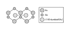
- FIG. 1 is a schematic view showing a ⁇ 110> dumbbell formed between GsAs crystal lattices.
- FIG. 2 is a schematic diagram showing that stabilizing the ⁇ 110> dumbbell suppresses clustering of interstitial As.
- FIG. 3 is a graph showing the formation energy in the neutral state of the ⁇ 110> dumbbell in GaAs and AlAs.
- FIG. 4 is a graph showing the binding energy in the neutral state of the ⁇ 110> dumbbell in GaAs and AlAs.
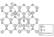
- FIG. 5 is a diagram illustrating a group III site, a group V site, a closest position of a dumbbell, and a second adjacent position of the dumbbell.
- FIG. 1 is a schematic view showing a ⁇ 110> dumbbell formed between GsAs crystal lattices.
- FIG. 2 is a schematic diagram showing that stabilizing the ⁇ 110> dumbbell suppresses clustering of interstitial As.
- FIG. 3 is a graph showing the formation energy in the neutral
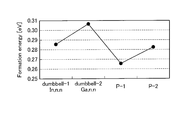
- FIG. 6 is a graph showing the formation energy of ⁇ 110> dumbbells in an In 0.6 Ga 0.4 As mixed crystal in a neutral state.
- FIG. 7 is a graph showing the formation energy of ⁇ 110> dumbbells in GaAs.
- FIG. 8 is a graph showing the size of the diffusion barrier between the lattices As.
- FIG. 9 is a diagram showing an observation image by TEM.
- FIG. 10 is a schematic diagram illustrating the semiconductor device according to the first embodiment.
- FIG. 11 is a graph showing the slope efficiency of the semiconductor laser device when the concentration of P in the active layer is changed.
- FIG. 12 is a schematic view showing a semiconductor device according to the second embodiment.
- FIG. 13 is a schematic view showing a semiconductor device according to the third embodiment.
- FIG. 14 is a schematic view showing a semiconductor device according to the fourth embodiment.
- FIG. 15 is a schematic view showing a semiconductor device according to the fifth embodiment.
- FIG. 16 is a schematic view showing a semiconductor device according to the sixth embodiment.
- FIG. 17 is a schematic view showing a semiconductor device according to the seventh embodiment.
- FIG. 18 is a schematic view showing a semiconductor device according to the eighth embodiment.
- FIG. 19 is a diagram showing an example in which P atoms are introduced digitally.
- gallium arsenide (GaAs) or aluminum arsenide (AlAs) is used as an example of a semiconductor crystal, but the implementation of the present invention is not limited to these examples, and III containing arsenic (As) as a main component.
- the present invention can be appropriately implemented in a semiconductor device using a ⁇ V group semiconductor crystal.
- the group III-V semiconductor crystal containing As as a main component includes AlGaAs, InGaAs, AlGaInAs, GaInNAs, AlGaInNAs, and the like.
- As being a V group main component means that the ratio of As to all V group elements in the composition elements of the III-V group semiconductor crystal is 95% or more.
- Al or Ga is a group III main component means that the ratio of Al or Ga to all group III elements in the composition elements of the group III-V semiconductor crystal is 95% or more.
- dislocation loop growth suppression mechanism First, let us consider the mechanism of dislocation loop formation. At that time, assuming uniform nucleation, the energy for forming dislocation loops in GaAs is the self energy of dislocations (sum of linear tension, dislocation core, and entropy term), stacking fault energy, and point defects. It depends on the balance between the degree of supersaturation and the chemical potential determined by the temperature of the system. However, when the formation energy was calculated using known physical quantities, it became clear that homogeneous nucleation was not a dislocation loop formation mechanism.
- Non-Patent Document 1 describes the relationship between the strain amount of a system and the structure of a point defect complex by performing heat treatment after growth on GaAs grown by a low temperature molecular beam epitaxy method. That is, the As interstitial atoms introduced during crystal growth progress to an assembly of As interstitial atom pairs, four interstitial As, and eight interstitial As with increasing heating temperature. . The strain of the system decreases as the aggregate of As interstitial atoms increases. This result means that the distortion of the entire system is alleviated by the formation of interstitial As clusters.
- the relaxation of strain originates from the presence of minute dislocation loops on the nanometer scale around the clusters present in the matrix. Such a small dislocation loop cannot be observed using a transmission electron microscope (TEM) or the like. However, when this dislocation loop grows by absorbing supersaturated point defects existing around it, its existence becomes obvious. When the growth of the dislocation loop further proceeds, the semiconductor device may eventually deteriorate and be destroyed. In particular, when a high load is applied to a semiconductor device, such as a high-power laser drive or a high electric field application, interstitial atoms are easily generated in the semiconductor crystal, and the interstitial atoms are easy to move. Growth is promoted. Such a dislocation loop grows in the bulk and causes deterioration of the characteristics of the semiconductor device.
- TEM transmission electron microscope
- FIG. 1 is a schematic view showing a ⁇ 110> dumbbell formed between GsAs crystal lattices.
- GaAs has a zinc blende type crystal structure composed of gallium atoms (Ga) and arsenic atoms (As).
- Ga gallium atoms
- As arsenic atoms
- the ⁇ 110> dumbbell is stable with As interstitial atoms paired in the ⁇ 110> direction.
- FIG. 2 is a schematic diagram showing that stabilizing the ⁇ 110> dumbbells suppresses the clustering of interstitial As in the (1-10) plane.
- FIG. 2 corresponds to an example in which phosphorus (P) is introduced into a group V site of a GaAs crystal lattice to be verified later, but ⁇ 110> dumbbell stabilization and interstitial As clustering suppression. The relationship is not limited to the case where P is introduced into the group V site.
- dumbbell stabilization contributes to the suppression of the generation of dislocation loops.
- the introduced impurity is a group III element or a group V element from the viewpoint of not adversely affecting electrical characteristics.
- the degree to which the ⁇ 110> dumbbell is stabilized depending on the type and position of atoms introduced, including not only P but also atoms such as nitrogen (N), indium (In), antimony (Sb), etc. will be verified. .
- E form per unit cell of the ⁇ 110> dumbbell depends on the charge state q and Fermi energy E f of the system, and is expressed by the following equation (2).
- E form (q, E f ) E tot [dumbbell] (q) ⁇ E tot [bulk] ⁇ n + qE f (2)
- ⁇ n is the chemical potential of the element n.
- ⁇ n has a different value depending on whether the growth condition is a group III (Ga / Al) rich condition or a group V (As) rich condition.
- E tot becomes the total energy E tot [dumbbell + impurity] (q) of the system including the impurity, and the addition of impurity atoms and the removal of Ga (Al) or As atoms are considered in terms of chemical potential.
- the impurity means an element such as P, N, Sb, or In introduced into the GaAs crystal or the AlAs crystal in order to suppress the formation of clusters of As interstitial atoms.
- the binding energy of the ⁇ 110> dumbbell was defined as the total energy of the system when the ⁇ 110> dumbbell was formed and the difference between the total energy of the system when two As interstitial atoms separated from each other existed.
- the main calculation conditions are as follows.
- ⁇ Atom model 64 atoms (Ga or Al: 32, As: 32) constituting the matrix, As atoms constituting dumbbells: 2, Impurity atoms introduced: 1 to 3 Cut-off energy: Wave function And charge density distribution, 30 Ry and 250 Ry, respectively
- K point sample 3 ⁇ 3 ⁇ 2 -Calculated number of bands: 200
- JAMSEC Japan Agency for Marine-Earth Science and Technology
- FIG. 3 is a graph showing the formation energy in a neutral state of ⁇ 110> dumbbells in GaAs and AlAs (Group III rich condition). Similar results can be obtained even under the V group rich condition.
- the vertical axis represents ⁇ 110> dumbbell formation energy (eV)
- the horizontal axis represents the type of element to be introduced.
- the results in GaAs are indicated by black circles, and the results in AlAs are indicated by hollow squares.
- FIG. 4 is a graph showing the binding energy in the neutral state of the ⁇ 110> dumbbell in GaAs and AlAs.
- the vertical axis represents the ⁇ 110> dumbbell binding energy (eV)
- the horizontal axis represents the type of element to be introduced.
- the results in GaAs are indicated by black circles, and the results in AlAs are indicated by hollow squares.
- the meanings of the ellipsis shown on the horizontal axis in the graphs of FIGS. 3 and 4 are as follows.
- the group III site, the group V site, the closest position of the dumbbell, and the second adjacent position of the dumbbell are as shown in FIG. Note that due to the three-dimensionality of the crystal structure, the closest position and the second proximity position are present on the front side and the back side of the paper, respectively.
- the formation energy of the ⁇ 110> dumbbell is lower than when not introduced.
- the effect when P is introduced is remarkable, and the formation energy is reduced by about 0.2 eV.
- the formation energy of ⁇ 110> dumbbells hardly changes or increases when Al or Ga is introduced.
- the introduction of In is less effective than P, but the formation energy decreases.
- the effect of reducing the formation energy becomes remarkable and a synergistic effect is obtained.
- the effect of reducing the formation energy is greater than the introduction of either N or P, and a synergistic effect is obtained.
- the effect of reducing dumbbell formation energy becomes remarkable when a plurality of P is introduced.
- the formation energy is reduced by about 0.3 eV.
- the effect is large in the model 3P (introduction of two P at the closest position of the dumbbell and one P at the second adjacent position).
- FIG. 6 is a graph showing the formation energy of ⁇ 110> dumbbells in an In 0.6 Ga 0.4 As mixed crystal in a neutral state. Calculations are performed under Group III rich conditions. In addition, in the group III site in the lattice, the In atom and the Ga atom are assumed to be randomly arranged.
- the vertical axis indicates the formation energy (eV) of ⁇ 110> dumbbells
- the horizontal axis indicates the type of element to be introduced.
- Model dumbbell-1 and model dumbbell-2 shown on the horizontal axis represent cases where In atoms and Ga atoms are arranged at the closest positions of the ⁇ 110> dumbbell, respectively.
- Model P-1 and model P-2 are obtained by introducing P into model dumbbell-1 and model dumbbell-2, respectively.
- the formation energy of the ⁇ 110> dumbbell decreases by about 20-30 meV.
- a model dumbbell-1 and a model P-1 having lower formation energy are formed in the vicinity of In atoms. This is because the effective shell charge of In atoms is high.
- InGaAs mixed crystals reflect the contribution of the effective shell charge of the In atoms constituting the matrix more greatly than GaAs and AlAs, as described above, so that the energy of ⁇ 110> dumbbell formation is 0 compared to GaAs and AlAs. It has decreased by about 1 to 0.25 eV. This means that in an AlGaAs mixed crystal, the concentration of As interstitial atoms alone is likely to be higher than in an InGaAs mixed crystal, and As clusters are likely to be formed, and the effect of introducing the impurities is higher. .
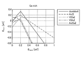
- FIG. 7 is a graph showing the formation energy of ⁇ 110> dumbbells in GaAs (Ga-rich condition).
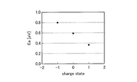
- the slope is a charged state, which is a donor when positive and an acceptor when negative.
- FIG. 7 shows other interstitial defects such as As interstitial atoms (As ⁇ I ⁇ ), Ga vacancies (V ⁇ Ga ⁇ ), As vacancies (V ⁇ As ⁇ ), As antisites.
- a graph of defects (As ⁇ Ga ⁇ ) is also shown.
- the graph of ⁇ 110> dumbbell formation energy and the graph of formation energy of As interstitial atoms intersect at a position where the Fermi energy is approximately 0.35 eV. Therefore, when the Fermi energy is higher than 0.35 eV, the formation energy of the ⁇ 110> dumbbell is lower than the formation energy of As interstitial atoms.
- the band gap of GaAs obtained by simulation is about 1 eV, and the Fermi energy in the intrinsic semiconductor is about 0.5 eV.
- the crossing of the formation energy of As interstitial atoms and the formation energy of ⁇ 110> dumbbell at 0.35 eV indicates that the ⁇ 110> dumbbell is stable unless a p-type impurity is intentionally added.
- the Fermi energy is about 0.5 eV, the formation energy of Ga vacancies and As vacancies that are acceptors is low, and if there are residual impurities such as carbon, the Fermi energy decreases.
- the n-type dopant concentration may be an amount that can cancel the compensation effect due to vacancies and residual impurities. For example, it is desirably 1 ⁇ 10 15 cm ⁇ 3 or more. Even if such a mixed crystal having n-type conductivity is formed as an n-type conductive region inside a region to function as a p-type semiconductor in a semiconductor device, for example, the n-type conductive region Among them, the effect that As interstitial atoms form ⁇ 110> dumbbells is more stable.
- Examples of n-type dopants include silicon (Si) and selenium (Se).
- FIG. 8 is a graph showing the size of the diffusion barrier of the interstitial As.
- the barrier Ea for the diffusion of a single As interstitial atom depends on the charged state, and is about 0.8 eV when the charged state is ⁇ 1 (in GaAs having n-type conductivity).
- the charge state is +1 (in GaAs having p-type conductivity)
- it is about 0.4 eV. That is, the barrier against diffusion of a single As interstitial atom is twice or more larger in GaAs having n-type conductivity than in GaAs having p-type conductivity.
- the example of GaAs in which no impurity is introduced has been described, but the same effect is obtained even when an impurity is introduced.
- the As interstitial diffusion barrier increases by about 10% (in the neutral state, increases by 50 meV). That is, the effect of suppressing the diffusion of As interstitial atoms becomes more remarkable by introducing P into GaAs and making the base conductivity n-type.
- Table 1 shown below is a table summarizing experimental results verifying the relationship between the concentration of P substituted at the group V element site, the formation of dumbbells, and the detection of As precipitates.
- the verification experiment shown in Table 1 is performed as follows.
- SIMS Secondary ion mass spectrometry
- primary ions beam-like ions
- secondary ions ions generated by collisions between the ions and the solid surface at the molecular / atomic level. It is a surface measurement method to detect with.
- SIMS has a spatial resolution of about 10 ⁇ m, but can quantitate P with a concentration of about 0.01%.
- SIMS is preferably used for, for example, a GaAs long cavity laser element.
- An example of a measuring apparatus that employs SIMS is Cameca's sector SIMS (IMS series).
- the atom probe method is used to measure the concentration of P.
- a region including a measurement target is processed into a needle shape (probe shape) using a focused ion beam (FIB) processing apparatus.
- FIB focused ion beam
- the constituent atoms are field evaporated from the tip of the sample processed into a probe shape, and the atomic mass is analyzed by measuring the time of flight of the field evaporated atoms.
- the atom probe method is used for a semiconductor, it is preferable to assist evaporation of atoms with a laser beam in order to prevent charge-up.
- This measuring method is suitable, for example, for measuring the P concentration in the active layer in an InP-based BH laser element. This is because the analysis range can be narrowed (for example, 1 ⁇ m or less) as compared with normal SIMS.
- An example of a measuring apparatus that employs this atom probe method is Cameca's LEAP series.
- the concentration of P is measured using a scanning tunneling microscope (STM).
- STM scanning tunneling microscope
- the measurement method using STM is suitable for both InP-based BH laser elements and GaAs-based ridge laser elements.
- a sample is cleaved in an ultrahigh vacuum to expose a cross section of the active layer, and an atomic image is observed by STM.
- STM applies a bias voltage of several volts between a probe whose tip curvature is on the order of nanometers and the sample surface, and feeds back a small tunnel current (about 1 nA or less), thereby obtaining an uneven image of atoms. It is a microscope. At this time, since the electronic state is different between the base Ga, As, etc. and P, there is a difference in the contrast of the image obtained by STM. Therefore, the concentration can be evaluated by counting the number of P atoms from the image obtained by STM. Examples of STMs that can be used in this measurement method include STM-1 and LT-STM manufactured by Omicron.
- the concentration of P can be determined from the measurement of the optical band gap by photoluminescence measurement or the measurement of the lattice constant by X-ray diffraction.
- ⁇ 110> dumbbells can be confirmed by, for example, Raman spectroscopic measurement. This is because a crystal in which ⁇ 110> dumbbells are formed has a Raman-active vibration mode caused by ⁇ 110> dumbbells. For example, using a third harmonic of an Ar ion laser with a wavelength of 488 nm or a YAG laser with a wavelength of 355 nm, the local vibration mode is measured at a position of 50 to 150 cm ⁇ 1 with respect to the LO mode of the mixed crystal constituting the active layer. By doing so, formation of ⁇ 110> dumbbells can be confirmed.
- dumbbells As a method for directly observing the formation of ⁇ 110> dumbbells, there is anisotropy measurement of strain by X-ray diffraction. This method enables high-precision measurement by using wavelength-variable radiation. After the waveguide structure on the active layer is removed by etching, the dependency of the lattice constant on the depth direction is measured by measuring a plurality of diffraction surfaces.
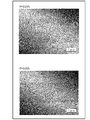
- the precipitate of As As for the precipitate of As, observation with a transmission electron microscope (TEM) is performed. Quantification of As precipitates is based on the number of observations based on a resonator length of 100 ⁇ m in a resonator having a width of 25 ⁇ m. For example, as shown in FIG. 9, when TEM observation is performed, the presence of As precipitates is recognized as in the broken-line circle. By quantifying the As precipitates detected in this way around a resonator length of 100 ⁇ m, the As precipitate is quantified. In addition, in the observation image by TEM shown in FIG. 9, the concentration of P is 0.01% or less (meaning that P is not substantially added, the same applies hereinafter) and the concentration of P is 0.02%. In this case, a part of the measurement range is cut out.
- TEM transmission electron microscope
- the local vibration mode due to the ⁇ 110> dumbbell is observed when the concentration of P in the crystal is 0.01% and 0.02%.
- the concentration of P in the crystal is 0.1% or more, it is considered that the stabilization of interstitial As by the ⁇ 110> dumbbells functions sufficiently.
- the concentration of P, N, or Sb substituted at the group V element site is preferably in the range of 0.02% or more with respect to the total amount of the group V element at the group V element site, 0.1% It is more preferable to be in the above range.
- the concentration of In substituted for the Group III element site is the entire Group III element at the Group III element site.
- a range of 0.1% or more with respect to the amount is preferable. In this range, the probability that the introduced impurity atoms are close to other P impurity atoms increases, and the model 2P-1 ( ⁇ 110> dumbbell closest position and the second position indicated on the horizontal axis in FIGS. This is because it is easy to realize a state in which P is arranged at a close position.
- the concentration of impurity atoms in the group V element is in the range of 0.1 to 5%, the formation energy of ⁇ 110> dumbbells is low and the binding energy is high.
- the concentration of impurity atoms added to the III-V group semiconductor crystal containing As as a main component is preferably 5% or less. This is because the initial characteristics are excellent when the impurity atom concentration is 5% or less.
- the initial characteristic is evaluated by the maximum value of the slope efficiency when the temperature is changed.
- the slope efficiency is defined by the slope of the current-light output characteristic, and its unit is [mW / mA].
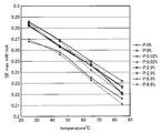
- Table 2 summarizes the verification results of the initial characteristics. As shown in Table 2, it can be seen that the initial characteristics are excellent when the concentration of impurity atoms is 5% or less. In particular, if the concentration of impurity atoms is 3% or less, no deterioration in the initial characteristics is measured.
- the energization and the current-light output characteristic measurement are repeated, and the increase rate of the threshold is measured.
- the increase rate of the threshold was measured under the acceleration condition of 120 ° C./150 mA
- the gradual deterioration was suppressed in the cases where the P concentration was 0.02%, 3%, and 5%.
- the increase rate of the threshold was measured under the acceleration condition of 155 ° C./125 mA
- the gradual deterioration was suppressed when the P concentration was 0.02% and 3%. Therefore, if the concentration of impurity atoms is 5% or less, the gradual deterioration is suppressed, and it is more preferable if the concentration of impurity atoms is 3% or less.
- the impurity atom concentration is 5% or less, the lattice constant difference and the band gap difference with the mixed crystal substrate are not large, so that the mobility is reduced due to misfit dislocation formation or alloy scattering, or two-dimensional electrons.
- the concentration is desirably 1% or less. This is because, when the concentration is higher than 1%, In is clustered and formation of ⁇ 110> dumbbells is prevented.
- the concentration of P, N, or Sb substituted at the group V element site is in the range of 0.02% to 5% with respect to the total amount of the group V element at the group V element site. It is preferable that it is 0.1% or more and 3% or less.
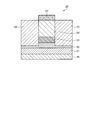
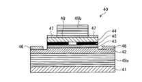
- FIG. 10 is a schematic diagram illustrating the semiconductor device according to the first embodiment.
- the semiconductor device shown in FIG. 10 is a semiconductor laser element using a buried heterostructure (BH) structure as a current confinement structure.
- FIG. 10 is a cross-sectional view parallel to the emission surface of this semiconductor laser element.
- BH buried heterostructure
- an n-type semiconductor layer 12 and an active layer 13 are sequentially stacked on a substrate 11.
- the upper part of the n-type semiconductor layer 12 and the active layer 13 have a mesa structure having a longitudinal direction in the emission direction.
- the active layer 13 has a multiple quantum well (MQW) structure including a well layer and a barrier layer.
- MQW multiple quantum well
- a p-type semiconductor layer 14 is laminated on the top of the n-type semiconductor layer 12 and the mesa structure formed of the active layer 13.
- An n-type semiconductor layer 15 as a current confinement structure is formed inside the p-type semiconductor layer 14 adjacent to both sides in the width direction of the mesa structure.
- an n-side electrode 16 is formed on the back surface of the substrate 11, and a p-side electrode 17 is formed on the surface of the p-type semiconductor layer 14.
- the n-type semiconductor layer 15 as a current confinement structure confines the current injected from the p-side electrode 17 inside, and confines the light generated from the active layer 13 in the lateral (width) direction, so that a high-order horizontal transverse mode is obtained. Responsible for the function to realize single transverse mode operation with suppressed.
- the well layer of the active layer 13 is a layer made of InGaAsP in which P is introduced into InGaAs.
- the barrier layer of the active layer 13 is made of AlGaAs and serves as a barrier function for confining carriers in the well layer.
- the active layer 13 is not limited to the above example, and may be formed of a III-V group semiconductor mainly composed of As such as GaAs, AlAs, AlGaAs, InGaAs, AlGaInAs, and GaInNAs.
- P is introduced only into the well layer of the active layer 13.
- P may be introduced into AlGaAs as the barrier layer, and P may be introduced into the entire active layer 13.
- the configuration of the active layer 13 is not limited to the multi-well structure, and any structure of the active layer 13 can suppress the occurrence of dislocation loops by introducing P.
- the impurity to be introduced is not limited to P, but may be N, Sb, or In.
- the active layer 13 Since the active layer 13 is in an active state when the semiconductor laser device 10 is driven, As interstitial atoms are easily formed and the As interstitial atoms are easily moved. Therefore, P, N, Introducing Sb or In is highly effective. In particular, when the active layer 13 has a multiple quantum well structure, it is the well layer that is activated when the semiconductor laser device 10 is driven. Therefore, P, N, Sb, or In is selectively applied only to the well layer. The effect is also great by introducing.
- the active layer 13 preferably has n-type conductivity. Therefore, it is preferable to add an n-type dopant to the active layer 13.
- the n-type dopant includes selenium (Se), sulfur (S), or silicon (Si).
- concentration of the n-type dopant of the active layer 13 is lower than the density
- the concentration of the n-type dopant in the active layer 13 is preferably 1 ⁇ 10 18 cm ⁇ 3 or less.
- the concentration is higher than 1 ⁇ 10 18 cm ⁇ 3
- the concentration of Ga vacancies and As vacancies in the semiconductor increases, so the binding energy of adjacent ⁇ 110> dumbbells decreases, and the effect of suppressing the diffusion of As interstitial atoms is reduced. It is because it falls. Further, it is desirable that the amount is sufficient to cancel the compensation effect of vacancies and residual impurities, for example, 1 ⁇ 10 15 cm ⁇ 3 or more.
- the other semiconductor layer is formed of a semiconductor having a higher band gap energy and a lower refractive index than the well layer of the active layer 13.
- the other semiconductor layer is preferably formed of a group III-V semiconductor containing As as a main component, but may be formed of, for example, InP.
- P, N, Sb, or In is selectively introduced into the p-type semiconductor layer 14 under the p-side electrode 17 or the n-type semiconductor layer 12 near the interface with the epitaxial substrate. This is also effective in suppressing the occurrence of dislocation loops. Further, selectively making the location where the dislocation loop is likely to occur n-type conductivity is also effective in suppressing the occurrence of the dislocation loop. As described above, the effect of suppressing the occurrence of dislocation loops can be obtained even if the semiconductor layer 10 has n-type conductivity as much as the intrinsic semiconductor.
- the semiconductor laser element 10 By creating a weak n-type conductive region that does not affect the function of the dislocation loop, the effect of suppressing the occurrence of dislocation loops can be obtained.
- Example 1 is a configuration embodying the first embodiment. Therefore, in the description of the first embodiment, the same FIG. 10 as that of the first embodiment is referred to. Moreover, the description which overlaps with description of 1st Embodiment is abbreviate
- the semiconductor laser device 10 according to Example 1 is a so-called AlInGaAsP-BH laser device on an InP substrate. Therefore, an n-type semiconductor layer 12 made of, for example, n-type InP and an active layer 13, for example, a p-type semiconductor layer 14 made of, for example, p-type InP are stacked on a substrate 11 made of InP.
- the active layer 13 has a mesa structure.
- the active layer 13 has an MQW structure in which a pair of a well layer and a barrier layer is laminated six times.
- a resonator width stripe width of the active layer 13
- a resonator length stripe length of the active layer 13
- the thicknesses of the well layer and the barrier layer are 6 nm and 10 nm, respectively, and the strain of the well layer and the barrier layer with respect to the InP substrate is 1% and ⁇ 0.3%, respectively.
- substrate is set as a positive distortion
- the case where it is small is set as a negative distortion.
- the composition of the active layer and the barrier layer of the active layer 13 is adjusted so that the oscillation wavelength is 1.55 ⁇ m.
- the composition of the active layer 13 in the case of different P concentrations is illustrated.
- the well layer is Al 0.058 In 0.676 Ga 0.267 As and the barrier layer is Al 0.206 In 0.488 Ga 0.306 As.
- the well layer is Al 0.054 In 0.68 Ga 0.265 As 0.99 P 0.01
- the barrier layer is Al 0.203. In 0.49 Ga 0.307 As 0.99 P 0.01 .
- the structure of the active layer 13 is such that the well layer is Al 0.048 In 0.69 Ga 0.262 As 0.97 P 0.03 , and the barrier layer Is Al 0.2 In 0.6 Ga 0.2 As 0.97 P 0.03 .
- the composition of group III Al, Ga, and In
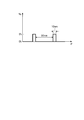
- FIG. 11 is a graph showing the slope efficiency of the semiconductor laser device when the concentration of P in the active layer is changed.
- data of two semiconductor laser elements having the same structure and composition are shown by a solid line and a broken line.
- the maximum value of the slope efficiency does not change until the concentration of P in the active layer is 3%.
- the maximum value of the slope efficiency at 25 ° C. is 0.28 to 0.29 mW / mA.
- the concentration of P in the active layer exceeds 5%, the slope efficiency decreases.
- the concentration of P in the active layer is 6.6%
- the maximum value of the slope efficiency at 25 ° C. is 0.22. It is ⁇ 0.23 mW / mA.
- the concentration of P in the active layer exceeds 10%, the slope efficiency at 25 ° C. is significantly lowered and becomes 0.2 mW / mA. Therefore, the semiconductor laser device 10 according to Example 1 has excellent initial characteristics.
- the threshold value of the active layer semiconductor laser element not added with P increases gradually after 1000 hours and increases by 10% or more after 2000 hours.
- the concentration of P in the active layer is 0.02%, 2.9%, and 6.6%, the gradual deterioration of the semiconductor laser element is suppressed.
- the increase rate of the threshold at 2000 hours is also 8% or less.
- the tendency of the threshold increase does not change, and the increase of the threshold is suppressed when the concentration is 0.02% and 2.9%, but in the example where P is not added.
- a 10% to 20% increase in threshold is measured.
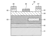
- FIG. 12 is a schematic view showing a semiconductor device according to the second embodiment.
- the semiconductor device shown in FIG. 12 is a semiconductor laser element using an SI-BH (Semi-Insulating Buried Heterostructure) structure.
- FIG. 12 is a cross-sectional view parallel to the emission surface of this semiconductor laser element.
- SI-BH Semi-Insulating Buried Heterostructure
- an n-type semiconductor layer 22, an active layer 23, and a p-type semiconductor layer 24 are sequentially stacked on a substrate 21.
- the upper part of the n-type semiconductor layer 22, the active layer 23, and the p-type semiconductor layer 24 have a mesa structure having a longitudinal direction in the emission direction.
- the active layer 23 has a multiple quantum well structure including a well layer and a barrier layer.
- a buried layer 25 made of a high-resistance material such as Fe—InP is formed on the n-type semiconductor layer 22 and on both sides of the mesa structure made of the active layer 23 and the p-type semiconductor layer 24. Further, an n-side electrode 26 is formed on the back surface of the substrate 21, and a p-side electrode 27 is formed on the surface of the p-type semiconductor layer 24.
- the buried layer 25 has a function of suppressing the spread of current flowing from the p-side electrode 27 to the n-side electrode 26 and confining light generated from the active layer 23 in the lateral (width) direction.
- the buried layer 25 is made of, for example, a semi-insulating III-V semiconductor doped with iron (Fe).
- the buried layer 25 is not limited to a semi-insulating III-V semiconductor doped with iron (Fe), but may be a semi-insulating III-V semiconductor doped with ruthenium (Ru).
- the well layer of the active layer 23 is a layer made of InGaAs 0.99 P 0.01 in which P is introduced into InGaAs.
- the barrier layer of the active layer 23 is made of AlGaAs and serves as a barrier function for confining carriers in the well layer.
- the active layer 23 is not limited to the above example, and may be formed of other group III-V semiconductors mainly composed of As.
- the configuration of the active layer 23 is not limited to the multi-well structure, and P can be introduced into the entire active layer, and the impurity to be introduced is not limited to P.
- the active layer 23 preferably has n-type conductivity. Therefore, it is preferable to introduce an n-type dopant into the active layer 23.
- concentration of the n-type dopant of the active layer 23 is lower than the density
- the concentration of the n-type dopant in the active layer 23 is preferably 1 ⁇ 10 18 cm ⁇ 3 or less, and preferably 1 ⁇ 10 15 cm ⁇ 3 or more.
- the other semiconductor layer is formed of a semiconductor having a higher band gap energy and a lower refractive index than the well layer of the active layer 23.
- the other semiconductor layer is preferably formed of a group III-V semiconductor containing As as a main component, but may be formed of, for example, InP.
- P, N, Sb, or In into all the semiconductor layers of the semiconductor laser element 20
- P, N, Sb, or In is selectively applied to a portion of the p-type semiconductor layer 24 under the p-side electrode 27 or a portion of the p-type semiconductor layer 24 near the interface with the buried layer 25.
- the introduction is also effective in suppressing the occurrence of dislocation loops.
- selectively making the location where the dislocation loop is likely to occur n-type conductivity is also effective in suppressing the occurrence of the dislocation loop.
- the effect of suppressing the occurrence of dislocation loops can be obtained even if the semiconductor layer 20 has n-type conductivity as much as the intrinsic semiconductor. Therefore, even if it is a p-type semiconductor layer of the semiconductor laser element 20, the semiconductor laser element 20 By creating a weak n-type conductive region that does not affect the function of the dislocation loop, the effect of suppressing the occurrence of dislocation loops can be obtained.
- FIG. 13 is a schematic view showing a semiconductor device according to the third embodiment.
- the semiconductor device shown in FIG. 13 is a semiconductor laser element using a ridge structure.
- FIG. 13 is a cross-sectional view parallel to the emission surface of this semiconductor laser element.
- an n-type semiconductor layer 32, an active layer 33, and a p-type semiconductor layer 34 are sequentially stacked on a substrate 31.
- the upper part of the p-type semiconductor layer 34 has a ridge structure having a longitudinal direction in the emission direction.
- the active layer 33 has a multiple quantum well structure including a well layer and a barrier layer.
- an IFVD (Impurity Free Vacancy Disordering) method which is an end face protection structure described in Patent Document 1, is applied to the active layer 33.
- the ridge structure bears the function of confining light generated from the active layer 33 in the lateral (width) direction by making a difference in the thickness of the p-type semiconductor layer 34 functioning as a cladding layer.
- An n-side electrode 36 is formed on the back surface of the substrate 31, and a p-side electrode 37 is formed on the surface of the p-type semiconductor layer 34.
- the well layer of the active layer 33 is a layer made of InGaAsP in which P is introduced into InGaAs.
- the barrier layer of the active layer 33 is made of AlGaAs and serves as a barrier function for confining carriers in the well layer.
- the active layer 33 is not limited to the above example, and may be formed of other group III-V semiconductors mainly composed of As. Further, similarly to the first embodiment, in this embodiment, the configuration of the active layer 33 is not limited to the multiple well structure, and P can be introduced into the entire active layer, and the impurity to be introduced is not limited to P.
- the active layer 33 preferably has n-type conductivity. Therefore, it is preferable to introduce an n-type dopant into the active layer 33.
- concentration of the n-type dopant of the active layer 33 is lower than the density
- the concentration of the n-type dopant in the active layer 33 is preferably 1 ⁇ 10 18 cm ⁇ 3 or less, and preferably 1 ⁇ 10 15 cm ⁇ 3 or more.
- the other semiconductor layer is formed of a semiconductor having a higher band gap energy and a lower refractive index than the well layer of the active layer 33.
- the other semiconductor layer is preferably formed of a group III-V semiconductor containing As as a main component, but may be formed of, for example, InP.
- P, N, Sb, or In is introduced into all the semiconductor layers of the semiconductor laser element 30, not only the active layer 33 but also P, N, A method of introducing Sb or In is also conceivable.
- P, N, Sb, or In is selectively introduced into a portion of the p-type semiconductor layer 34 under the p-side electrode 37 or a portion of the p-type semiconductor layer 34 that becomes the rising portion of the ridge structure. This is also effective in suppressing the occurrence of dislocation loops. Further, selectively making the location where the dislocation loop is likely to occur n-type conductivity is also effective in suppressing the occurrence of the dislocation loop.
- the effect of suppressing the occurrence of dislocation loops can be obtained even if the semiconductor layer 30 has an n-type conductivity as much as the intrinsic semiconductor. Therefore, even if it is a p-type semiconductor layer of the semiconductor laser element 30, the semiconductor laser element 30 By creating a weak n-type conductive region that does not affect the function of the dislocation loop, the effect of suppressing the occurrence of dislocation loops can be obtained.
- the IFVD method when the laser output is about 1 W or less, the deterioration mode due to the end face is suppressed without adding P, N, Sb, or the like.
- the semiconductor laser device 30 in addition to the IFVD method being applied, P, N, Sb, or the like is introduced into the active layer 33 or the like, so that the CW having an optical output of several tens W or more Even under driving conditions, the occurrence of dislocation loops in the bulk as well as the end face is suppressed.
- Example 2 is a configuration embodying the third embodiment. Therefore, in description of Example 2, FIG. 13 same as 3rd Embodiment is referred. Moreover, the description which overlaps with description of 1st Embodiment is abbreviate
- the semiconductor laser device 30 according to the second embodiment is a ridge laser device on a so-called GaAs substrate. Therefore, an n-type semiconductor layer 32 made of, for example, n-type AlGaAs and an active layer 33, eg, a p-type semiconductor layer 34 made of, for example, p-type AlGaAs are stacked on a substrate 31 made of GaAs.
- the ridge structure has a longitudinal direction in the emission direction.
- the active layer 33 has an SQW (Single Quantum Well) structure in which a well layer is sandwiched between barrier layers.
- SQW Single Quantum Well
- a light output of about 12 W can be achieved with one chip when the drive (rated) current is 12 A.
- the thicknesses of the well layer and the barrier layer are 10 nm and 30 nm, respectively, and P is added to the active layer while adjusting the composition of the well layer and the barrier layer so that the oscillation wavelength is 910 nm.
- an oscillation wavelength of 910 nm can be realized by setting the well layer to In 0.075 Ga 0.925 As and the barrier layer to Al 0.32 Ga 0.68 As. Further, in the example of the active layer to which P is added at a concentration of 3%, the well layer is In 0.1 Ga 0.9 As 0.97 P 0.03 , and the barrier layer is Al 0.31 Ga 0.69 As. An oscillation wavelength of 910 nm can be realized by setting 0.97 P 0.03 . In this way, the Group III composition is adjusted, and the concentration of P added so as to make the wavelength constant is changed in the range of 0.02 to 10%.
- the initial characteristics are evaluated using a semiconductor laser device in which the concentration of P added as described above is changed in the range of 0.02 to 10%.
- the initial characteristics are evaluated by the maximum value of the slope efficiency at room temperature (25 ° C.).
- the slope efficiency is in the range of 1.01 to 1.02 W / A in any semiconductor laser element including the case where P is not added. Good initial characteristics can be obtained.
- the slope efficiency is reduced to about 1 W / A.
- the slope efficiency is reduced to 0.9 W / A or less.
- the semiconductor laser device it is desirable to configure the semiconductor laser device so that the concentration of P added to the active layer is 3% or less.
- the optical output of the semiconductor laser element was monitored while energizing a constant current of 12 A at an ambient temperature of 25 ° C.
- the optical output was exceeded after 1000 hours in the semiconductor laser element in which P was not added to the active layer. Decrease is observed.
- the semiconductor laser device in which P is added to the active layer at a concentration of 0.02% the light output is not reduced until 2000 hours.
- the semiconductor laser device in which P is added to the active layer at a concentration of 0.1% or more no decrease in light output is observed even after 2000 hours.
- Example 3 is obtained by changing the composition of the active layer in the configuration of Example 2. Therefore, only the composition of the active layer will be described here, and description of other components will be omitted.
- the active layer in Example 3 includes Al in the well layer and In in the barrier layer.
- the well layer is made of Al 0.05 In 0.15 Ga 0.8 As 0.97 P 0.03
- the barrier layer is made of Al 0.35 In 0.05.
- Ga 0.6 As 0.97 P 0.03 an oscillation wavelength of 910 nm is realized.
- the group III composition is adjusted, and the concentration of P added so as to make the wavelength constant is changed in the range of 0.02 to 10%.
- Example 3 the initial characteristics at room temperature (25 ° C.) are evaluated.
- the slope efficiency is in the range of 1.01 to 1.02 W / A in any semiconductor laser element including the case where P is not added.
- Good initial characteristics can be obtained. That is, the initial characteristic value at 25 ° C. is not significantly different between Example 2 and Example 3.
- the value of the initial characteristic at 50 ° C. is superior to that of the semiconductor laser device of Example 3 over Example 2. That is, the slope efficiency of Example 3 is improved by about 5% compared to the semiconductor laser element of Example 2. This is presumably because the band gaps of the well layer and the barrier layer were designed to be the same in Example 2 and Example 3, but the difference in group III composition between them caused a difference in electron affinity. The difference is 15 meV for the well layer and 19 meV for the barrier layer. As a result, in Example 3, it is considered that carrier leakage from the well layer at a high temperature was suppressed, and the slope efficiency was improved.
- Examples 2 and 3 an example of a semiconductor laser device having an oscillation wavelength of 910 nm is shown.
- the composition of the group III element may be changed as appropriate.
- the well layer of the active layer is made of Al 0.05 In 0.25 Ga 0.7 As 0.97 P 0.03
- the barrier layer is made of Al 0. 35 In 0.05 Ga 0.6 As 0.97 P 0.03 may be used.
- FIG. 14 is a schematic view showing a semiconductor device according to the fourth embodiment.
- the semiconductor device shown in FIG. 14 is a vertical cavity surface emitting laser (VCSEL) type semiconductor laser element (hereinafter referred to as a surface emitting laser element).
- VCSEL vertical cavity surface emitting laser
- FIG. 14 is a cross-sectional view of the semiconductor laser element with respect to the emission direction.
- a layer 48 and an upper DBR mirror 49b are sequentially stacked.
- the upper end portion of the n-type semiconductor layer 42, the active layer 43, the current confinement layer 45, and the p-type semiconductor layer 44 are formed as mesa posts formed into a columnar shape by an etching process or the like. Yes.
- the n-side electrode 46 is disposed on the surface of the n-type semiconductor layer 42 exposed as a mesa post, and the p-side electrode 47 surrounds the phase adjustment layer 48 on the surface of the p-type semiconductor layer 44 that is the upper end of the mesa post. It is installed like a ring.
- the lower DBR mirror 49a is formed as a semiconductor multilayer mirror in which a plurality of composite semiconductor layers made of, for example, AlAs / GaAs are stacked.
- the thickness of each layer constituting this composite semiconductor layer is ⁇ / 4n ( ⁇ : oscillation wavelength, n: refractive index).
- the upper DBR mirror 49b is formed as a dielectric multilayer mirror in which a plurality of composite dielectric layers made of, for example, SiN / SiO 2 are stacked, and the thickness of each layer is ⁇ / 4n as in the lower DBR mirror 49a. It is said that.
- the current confinement layer 45 is composed of an opening and an oxidized constriction.
- the current confinement layer 45 is formed by an Al-containing layer made of, for example, AlAs, and the oxidized constriction portion is formed by oxidizing the Al-containing layer by a predetermined range from the outer peripheral portion.
- the oxidized constriction portion has an insulating property, and the current density in the active layer 43 is increased by constricting the current injected from the p-side electrode 47 and concentrating it in the opening.
- the active layer 43 has a multiple quantum well structure including a well layer and a barrier layer, and emits emitted light based on a current injected from the p-side electrode 47 and constricted by the current confinement layer 45.
- the emitted light is amplified by being resonated and amplified in a direction perpendicular to each layer including the active layer 43 between the lower DBR mirror 49a and the upper DBR mirror 49b as a resonator, and then laser is emitted from the upper surface of the upper DBR mirror 49b. Injected as light.
- the phase adjustment layer 48 provided between the p-type semiconductor layer 44 and the upper DBR mirror 49b is for adjusting the positions of antinodes and nodes of the standing wave of the laser beam formed in the resonator. is there.
- the well layer of the active layer 43 is a layer made of InGaAs 0.99 P 0.01 in which P is introduced into InGaAs.
- the barrier layer of the active layer 43 is made of AlGaAs and serves as a barrier function for confining carriers in the well layer.
- the active layer 43 is not limited to the above example, and may be formed of other group III-V semiconductors mainly composed of As. Further, similarly to the first embodiment, in this embodiment, the configuration of the active layer 43 is not limited to the multi-well structure, and P can be introduced into the entire active layer, and the impurity to be introduced is not limited to P.
- the active layer 43 preferably has n-type conductivity. Therefore, it is preferable to introduce an n-type dopant into the active layer 43.
- the n-type dopant is Se, S, or Si.
- concentration of the n-type dopant of the active layer 43 is lower than the density
- the concentration of the n-type dopant in the active layer 43 is preferably 1 ⁇ 10 18 cm ⁇ 3 or less, and when it is 1 ⁇ 10 15 cm ⁇ 3 or more, the effect of suppressing the occurrence of dislocation loops becomes significant.
- FIG. 15 is a schematic view showing a semiconductor device according to the fifth embodiment.
- the semiconductor device shown in FIG. 15 is a heterojunction transistor (HFET).
- FIG. 15 is a cross-sectional view crossing each electrode of the heterojunction transistor.
- the heterojunction transistor 50 includes a substrate 51 made of semi-insulating GaAs and a 1 ⁇ m-thick buffer made of undoped GaAs for relaxing lattice mismatch formed on the substrate 51.
- a layer 54 and a contact layer 55 made of n + -type GaAs having a thickness of 100 nm are sequentially stacked.
- P is introduced as described above, but the same effect can be obtained by introducing Sb, N or In in addition to P. Further, In and P may be doped at the same time.
- a source electrode 56 and a drain electrode 57 are formed on the contact layer 55.
- the contact layer 55 is etched to a depth at which the surface of the electron supply layer 54 is exposed, and a gate electrode 58 is formed.
- the outline of the method for manufacturing the heterojunction transistor 50 having the above-described configuration is as follows.
- the buffer layer 52, the electron transit layer 53, the electron supply layer 54, and the contact layer 55 are sequentially epitaxially grown using the MOCVD method or the MBE method to form an epitaxial layer.
- a pattern is formed with a photoresist to protect a predetermined position, and the contact layer 55 is removed by performing wet etching on the epitaxial layer using, for example, a mixed solution of phosphoric acid, hydrogen peroxide solution, and water.
- a mixed solution of phosphoric acid, hydrogen peroxide solution, and water is exposed to form a gate electrode formation portion.
- a pattern is formed with a new photoresist, an ohmic metal made of a Ni / AuGe alloy is deposited, and lift-off is performed to form the source electrode 56 and the drain electrode 57. Further, a gate electrode 58 made of Ti / Pt / Au is formed on the surface of the electron supply layer 54 by a similar photolithography process. Thus, the heterojunction transistor 50 having the above configuration is manufactured.
- the heterojunction transistor 50 having the above configuration is excellent in long-term reliability as compared with a heterojunction transistor having a conventional structure. Specifically, the increase in on-resistance over time is suppressed, and the device life is extended. This is because P is introduced into the electron transit layer 53 in the heterojunction transistor 50. The heat generated when the heterojunction transistor 50 is energized and the concentration of the electric field between the gate and the drain at the time of interruption are likely to cause diffusion of As interstitial atoms. However, since P is introduced into the electron transit layer 53, As Diffusion of interstitial atoms is suppressed, As clusters are not formed, and as a result, generation of dislocation loops is suppressed.
- the P composition of GaAsP in the electron transit layer 53 is preferably in the range of 0.01 to 5%. Since the concentration of As interstitial atoms generated when the electric field stress applied to the device is high and characteristic variation starts to occur is about 1 ⁇ 10 19 cm ⁇ 3 , the P concentration is higher than the As interstitial atoms at this concentration. Is high (for example, 0.01% or more), the probability of ⁇ 110> dumbbell formation increases.
- FIG. 16 is a schematic view showing a semiconductor device according to the sixth embodiment.
- the semiconductor device shown in FIG. 16 is a heterojunction transistor (HFET), which is a modification of the fifth embodiment.
- FIG. 16 is a cross-sectional view crossing each electrode of the heterojunction transistor.
- this embodiment is a modification of 5th Embodiment, below, only a different point from 5th Embodiment is demonstrated.
- the heterojunction transistor 60 includes a substrate 61 made of semi-insulating GaAs and a 1 ⁇ m-thick buffer composed of undoped GaAs for relaxing lattice mismatch formed on the substrate 61.
- An electric layer composed of a layer 62, a 100 nm thick electron transit layer 63 made of undoped GaAs 0.99 P 0.01, and Al 0.3 Ga 0.7 As doped with Si, which is an n-type impurity ion.
- a supply layer 64 and a contact layer 65 made of n + -type GaAs having a thickness of 100 nm are sequentially stacked.
- a partial n-type layer 69 made of GaAs 0.99 P 0.01 having n ⁇ -type conductivity is formed in a part of the electron transit layer 63.
- the partial n-type layer 69 may be formed, for example, at a thickness of 30 nm, for example, in the intermediate portion of the electron transit layer 63 in the thickness (longitudinal) direction of the epitaxial layer. Further, in the lateral direction, it may be formed at the lower part between the gate and the drain where the electric field concentration is likely to occur and the concentration of As interstitial atoms is increased.
- the partial n-type layer 69 may be formed by selective growth or ion implantation.
- the concentration of the n-type dopant in the partial n-type layer 69 is preferably lower than the concentration of the n-type dopant in the other n-type semiconductor layers.
- the concentration of the n-type dopant in the partial n-type layer 69 is preferably 1 ⁇ 10 18 cm ⁇ 3 or less, and the effect is remarkable when it is 1 ⁇ 10 15 cm ⁇ 3 or more.
- the concentration is higher than 1 ⁇ 10 18 cm ⁇ 3
- the concentration of Ga vacancies and As vacancies in the semiconductor increases, so the binding energy of adjacent ⁇ 110> dumbbells decreases, and the effect of suppressing the diffusion of As interstitial atoms is reduced. It is because it falls. Further, this is because 1 ⁇ 10 15 cm ⁇ 3 or more is a sufficient amount to cancel the compensation effect of vacancies and residual impurities.
- the heterojunction transistor 60 in which the partial n-type layer 69 is provided at the position as described above has a high diffusion barrier of As interstitial atoms in the vicinity of the position where As interstitial atoms are generated, and thus suppresses fluctuations in characteristics due to diffusion. can do.
- FIG. 17 is a schematic view showing a semiconductor device according to the seventh embodiment.
- the semiconductor device shown in FIG. 17 is a radiation detection PIN diode.
- FIG. 17 is a cross-sectional view crossing each electrode of the PIN diode.
- the PIN diode 70 includes a substrate 71, a buffer layer 72 formed on the substrate 71, an i-type (Intrinsic) layer 73 formed on the buffer layer 72, and an i-type layer 73.
- the substrate 71 is made of semi-insulating GaAs.
- the buffer layer 72 is made of undoped GaAs having a thickness of 1 ⁇ m, and is a layer for relaxing lattice mismatch.
- the i-type layer 73 is an i-type semiconductor layer made of GaAs 0.99 P 0.01 having a thickness of 1 ⁇ m in which P is introduced into GaAs.
- the p-type layer 74 and the n-type layer 75 are p-type and n-type semiconductor layers formed by, for example, ion implantation, selective growth, or thermal diffusion with respect to GaAs.
- the anode electrode 76 can be Ti / Pt / Au, and the cathode electrode 77 can be Ni / Au.
- the interval between the anode electrode and the cathode electrode is, for example, 10 ⁇ m.
- the PIN diode 70 when a reverse voltage is applied to the anode electrode 76 and the cathode electrode 77, a depletion layer expands in the i-type layer 73. When radiation enters the depletion layer, electron-hole pairs are formed along the path of the radiation. If the PIN diode 70 is used, radiation can be detected by detecting the pulse current generated at this time.
- the detection sensitivity of radiation is proportional to the fifth power of the atomic number and the density
- forming a PIN diode with GaAs realizes a sensitivity of 100 times or more than that of a Si PIN diode, and the sensitivity is comparable to that of a Ge detector.
- the band gap of GaAs is larger than that of Si, it is advantageous for a Ge detector that operates stably at room temperature and must use liquid nitrogen.
- the mobility of GaAs at room temperature is about 8000 cm 2 / Vs, and a response speed five times that of Si can be expected.
- the conductivity is not affected because P is a group V element.
- the i-type layer 73 of this embodiment is not intentionally added with a p-type dopant. Therefore, the i-type layer 73 corresponds to a region where the Fermi energy in FIG. 7 is about 0.5 eV, and a state of forming a ⁇ 110> dumbbell is realized rather than an As interstitial atom being present alone.
- the concentration of the P element in the group V element in the i-type layer 73 is preferably 0.1 to 5%. If it is 0.1% or more, the effect of forming the ⁇ 110> dumbbell is high.
- FIG. 18 is a schematic view showing a semiconductor device according to the eighth embodiment.
- the semiconductor device shown in FIG. 18 is a vertical PIN diode for radiation detection.
- FIG. 18 is a cross-sectional view crossing each electrode of the vertical PIN diode.
- the vertical PIN diode 80 includes a substrate 81, a buffer layer 82 formed on the substrate 81, an i-type layer 83 formed on the buffer layer 82, and an i-type layer 83.
- the substrate 81 is made of GaAs having n-type conductivity.
- the buffer layer 82 is made of GaAs having a thickness of 1 ⁇ m having n-type conductivity, and is a layer for relaxing lattice mismatch.
- the i-type layer 83 is an i-type semiconductor layer made of GaAs 0.99 P 0.005 having a thickness of 100 ⁇ m in which P is introduced into GaAs.
- the p-GaAs layer 84 is formed in the i-GaAsP layer 83.
- An anode electrode 85 is formed on the p-GaAs layer 84, and a cathode electrode 86 is formed on the back surface of the substrate 81.
- the p-type layer 84 is a p-type semiconductor layer formed by, for example, ion implantation, selective growth, or thermal diffusion with respect to GaAs.
- the anode electrode 85 can be Ti / Pt / Au and the cathode electrode 86 can be Ni / Au.
- FIG. 19 shows the growth direction (thickness direction) of the i-type layer and the P concentration at that position. A portion where the P concentration is 0% corresponds to GaAs.
- an undoped layer is formed by alternately repeating a GaAsP layer and a GaAs layer having a composition of 0.05 at a thickness of 10 nm and 90 nm, respectively.
- a GaAsP layer By digitally forming a GaAsP layer, it is possible to form a region having a high P concentration locally. In the region where the P concentration is high, the ⁇ 110> dumbbell is formed at a position where a plurality of P atoms are present, and the formation energy decreases and the binding energy increases. For this reason, the effect of suppressing the diffusion of As interstitial atoms is enhanced. In addition, when a GaAsP layer is formed digitally, it is possible to suppress misfit dislocations and occurrence of cracks rather than stacking a uniform concentration GaAsP layer, and the crystal quality of the epitaxial film is improved.
- the vertical PIN diode 80 of this embodiment can increase the thickness of the depletion layer 10 times compared to the PIN diode 70 of the seventh embodiment, so that the sensitivity of radiation can be increased about 10 times. Further, since the cathode electrode 86 is on the back surface of the substrate 81, the element area can be reduced, and there is an advantage that integration of a two-dimensional detector or the like is facilitated. At the same time, in the vertical PIN diode 80 of the present embodiment, since P is introduced into the i-type layer, ⁇ 110> dumbbells are easily formed, and the diffusion of As interstitial atoms is suppressed. For this reason, the vertical PIN diode 80 of the present embodiment is superior in long-term reliability than the conventional PIN diode.
- the semiconductor device according to the present invention is useful as a semiconductor device with little variation in characteristics.
Abstract
This semiconductor device is provided with a semiconductor layer comprising a group III-V crystalline semiconductor with As as the primary component, and a group V element other than As is introduced with a concentration of 0.02-5% at the group V site of the group III-V crystalline semiconductor in the semiconductor layer. Preferably, the group V element other than As is N, P or Sb, or a combination of these. Thereby, a semiconductor device is provided which keeps defects from occurring in the bulk crystalline semiconductor and which has less variation of characteristics.
Description
本発明は、半導体装置に関する。
The present invention relates to a semiconductor device.
半導体レーザ素子などの半導体装置には通電に伴う特性の劣化がある。たとえば、端面発光型レーザ素子においては、端面の光学的破壊(Catastrophic Optical Damage:COD)が発生することが知られている。CODを防止するための技術として、端面におけるレーザ光の吸収を抑制するための窓構造が知られている(特許文献1参照)。
Semiconductor devices such as semiconductor laser elements have characteristics that deteriorate with energization. For example, it is known that end face optical laser (Catastrophic Optical Damage: COD) occurs in the edge emitting laser element. As a technique for preventing COD, a window structure for suppressing absorption of laser light at an end face is known (see Patent Document 1).
半導体装置の特性劣化は、その端面の劣化によるものに注目が集まっていた。したがって、半導体素子の特性劣化への対策は、半導体装置の端面を保護する技術を中心として進展してきた。
The attention has been focused on the deterioration of the characteristics of the semiconductor device due to the deterioration of its end face. Therefore, countermeasures against the deterioration of the characteristics of the semiconductor element have been developed centering on the technology for protecting the end face of the semiconductor device.
しかしながら、本発明者らの検討したところによれば、半導体装置の高出力化、あるいは高耐圧化に伴い、半導体装置の端面のみならず、半導体結晶のバルク内においても特性劣化の原因となる欠陥が発生してしまう場合がある。例えば、半導体レーザ素子の活性層やその周辺では、バルク内に端面が起因でない転位ループが発生し、この転位ループが成長している様子が本発明者らにより確認されている。特に光出力が1チップでおよそ数10W以上となる高出力素子でこの傾向は顕著である。
However, according to a study by the present inventors, a defect that causes characteristic deterioration not only in the end face of the semiconductor device but also in the bulk of the semiconductor crystal as the output of the semiconductor device is increased or the breakdown voltage is increased. May occur. For example, it has been confirmed by the present inventors that a dislocation loop not caused by an end face is generated in the bulk in the active layer of the semiconductor laser element and its periphery, and this dislocation loop grows. In particular, this tendency is remarkable in a high-power element in which the light output is about several tens of watts or more per chip.
本発明は、上記に鑑みてなされたものであって、その目的は、半導体結晶のバルク内における欠陥発生を抑制し、特性の変動の少ない半導体装置を提供することにある。
The present invention has been made in view of the above, and an object of the present invention is to provide a semiconductor device that suppresses the occurrence of defects in the bulk of a semiconductor crystal and has little fluctuation in characteristics.
上述した課題を解決し、目的を達成するために、本発明の一態様に係る半導体装置は、AsをV族の主成分とするIII-V族半導体結晶からなる半導体層を備えた半導体装置であって、前記半導体層におけるIII-V族半導体結晶のV族サイトに、前記As以外のV族元素が濃度0.02~5%で導入されていることを特徴とする。
In order to solve the above-described problems and achieve the object, a semiconductor device according to one embodiment of the present invention is a semiconductor device including a semiconductor layer including a group III-V semiconductor crystal whose main component is As. In the semiconductor layer, a group V element other than As is introduced at a concentration of 0.02 to 5% into a group V site of a group III-V semiconductor crystal.
本発明の一態様に係る半導体装置は、前記As以外のV族元素は、N、P、Sbの何れかまたはこれらの組み合わせであることを特徴とする。
The semiconductor device according to one embodiment of the present invention is characterized in that the group V element other than As is any one of N, P, and Sb, or a combination thereof.
本発明の一態様に係る半導体装置は、前記AsをV族の主成分とするIII-V族半導体結晶は、InGaAs、AlGaInAs、GaInNAs、AlGaInNAsの何れかであることを特徴とする。
The semiconductor device according to one embodiment of the present invention is characterized in that the group III-V semiconductor crystal containing As as a main component of group V is any one of InGaAs, AlGaInAs, GaInNAs, and AlGaInNAs.
本発明の一態様に係る半導体装置は、前記AsをV族の主成分とするIII-V族半導体結晶は、GaAs、AlAs、AlGaAsの何れかであることを特徴とする。
The semiconductor device according to one aspect of the present invention is characterized in that the group III-V semiconductor crystal containing As as a main component of group V is any one of GaAs, AlAs, and AlGaAs.
本発明の一態様に係る半導体装置は、前記半導体層におけるIII-V族半導体結晶のIII族サイトに、濃度が0.1~1%でInが導入されていることを特徴とする。
The semiconductor device according to one embodiment of the present invention is characterized in that In is introduced at a concentration of 0.1 to 1% into a group III site of a group III-V semiconductor crystal in the semiconductor layer.
本発明の一態様に係る半導体装置は、前記半導体層は、n型ドーパントが添加されていることを特徴とする。
The semiconductor device according to one embodiment of the present invention is characterized in that an n-type dopant is added to the semiconductor layer.
本発明の一態様に係る半導体装置は、前記n型ドーパントの濃度は、1×1018cm-3以下1×1015cm-3以上であることを特徴とする。
In the semiconductor device according to one embodiment of the present invention, the concentration of the n-type dopant is 1 × 10 18 cm −3 or less and 1 × 10 15 cm −3 or more.
本発明の一態様に係る半導体装置は、前記半導体層は、半導体レーザ素子における活性層であることを特徴とする。
The semiconductor device according to one embodiment of the present invention is characterized in that the semiconductor layer is an active layer in a semiconductor laser element.
本発明の一態様に係る半導体装置は、前記As以外のV族元素は、多重量子井戸構造を有する前記活性層の井戸層に導入されていることを特徴とする。
The semiconductor device according to one embodiment of the present invention is characterized in that a group V element other than the As is introduced into a well layer of the active layer having a multiple quantum well structure.
本発明の一態様に係る半導体装置は、前記As以外のV族元素は、多重量子井戸構造を有する前記活性層の障壁層に導入されていることを特徴とする。
The semiconductor device according to one embodiment of the present invention is characterized in that a group V element other than the As is introduced into the barrier layer of the active layer having a multiple quantum well structure.
本発明の一態様に係る半導体装置は、前記活性層は、前記半導体レーザ素子における他のn型半導体層よりもn型ドーパントの濃度が低いことを特徴とする。
The semiconductor device according to one embodiment of the present invention is characterized in that the active layer has an n-type dopant concentration lower than other n-type semiconductor layers in the semiconductor laser element.
本発明の一態様に係る半導体装置は、前記半導体層は、ヘテロ接合トランジスタにおける電子走行層であることを特徴とする。
The semiconductor device according to one embodiment of the present invention is characterized in that the semiconductor layer is an electron transit layer in a heterojunction transistor.
本発明の一態様に係る半導体装置は、前記半導体層は、PINダイオードにおけるアンドープ層であることを特徴とする。
The semiconductor device according to one embodiment of the present invention is characterized in that the semiconductor layer is an undoped layer in a PIN diode.
本発明に係る半導体装置は、半導体結晶のバルク内における欠陥発生を抑制するという効果を奏する。
The semiconductor device according to the present invention has an effect of suppressing the occurrence of defects in the bulk of the semiconductor crystal.
以下、本発明の実施形態について図面を参照しつつ説明する。なお、以下の実施形態の全図においては、同一または対応する部分には同一の符号を付す。また、本発明は以下に説明する実施形態によって限定されるものではない。さらに、図面は模式的なものであり、各要素の寸法の関係などは、現実のものとは異なる場合があることに留意する必要がある。図面の相互間においても、互いの寸法の関係や比率が異なる部分が含まれている場合がある。
Hereinafter, embodiments of the present invention will be described with reference to the drawings. In all the drawings of the following embodiments, the same or corresponding parts are denoted by the same reference numerals. Further, the present invention is not limited to the embodiments described below. Furthermore, it should be noted that the drawings are schematic, and dimensional relationships between elements may differ from actual ones. Even between the drawings, there are cases in which portions having different dimensional relationships and ratios are included.
はじめに、本発明の実施形態について説明するにあたり、本発明の理解を容易にするために、上述した課題を解決すべく本発明者が行った鋭意検討について説明する。
First, in describing embodiments of the present invention, in order to facilitate understanding of the present invention, an intensive study conducted by the present inventor to solve the above-described problems will be described.
なお、以下では、半導体結晶の例としてヒ化ガリウム(GaAs)またはヒ化アルミニウム(AlAs)を用いるが、本発明の実施はこれらの例に限定されず、ヒ素(As)を主成分とするIII-V族半導体結晶を用いた半導体装置において、本発明を適切に実施することが可能である。例えば、Asを主成分とするIII-V族半導体結晶とは、AlGaAs、InGaAs、AlGaInAs、GaInNAs、AlGaInNAsなどが含まれる。ここで、AsがV族の主成分であるとは、III-V族半導体結晶の組成元素のうち、すべてのV族元素に対するAsの割合が95%以上であることを意味する。同様に、AlまたはGaがIII族の主成分であるとは、III-V族半導体結晶の組成元素のうち、すべてのIII族元素に対するAlまたはGaの割合が95%以上であることを意味する。
In the following, gallium arsenide (GaAs) or aluminum arsenide (AlAs) is used as an example of a semiconductor crystal, but the implementation of the present invention is not limited to these examples, and III containing arsenic (As) as a main component. The present invention can be appropriately implemented in a semiconductor device using a −V group semiconductor crystal. For example, the group III-V semiconductor crystal containing As as a main component includes AlGaAs, InGaAs, AlGaInAs, GaInNAs, AlGaInNAs, and the like. Here, As being a V group main component means that the ratio of As to all V group elements in the composition elements of the III-V group semiconductor crystal is 95% or more. Similarly, that Al or Ga is a group III main component means that the ratio of Al or Ga to all group III elements in the composition elements of the group III-V semiconductor crystal is 95% or more. .
(転位ループ成長抑制のメカニズム)
まず、転位ループの形成メカニズムについて考える。その際、均一核生成を仮定した場合、GaAs中に転位ループを形成するためのエネルギーは、転位の自己エネルギー(線張力、転位芯、およびエントロピー項の和)と、積層欠陥エネルギーと点欠陥の過飽和度と系の温度で決まる化学ポテンシャルと、の釣り合いによって決まる。しかしながら、公知の物理量を用いて形成エネルギーを計算したところ、均一核生成は転位ループの形成メカニズムではないことが明らかとなった。 (Dislocation loop growth suppression mechanism)
First, let us consider the mechanism of dislocation loop formation. At that time, assuming uniform nucleation, the energy for forming dislocation loops in GaAs is the self energy of dislocations (sum of linear tension, dislocation core, and entropy term), stacking fault energy, and point defects. It depends on the balance between the degree of supersaturation and the chemical potential determined by the temperature of the system. However, when the formation energy was calculated using known physical quantities, it became clear that homogeneous nucleation was not a dislocation loop formation mechanism.
そこで、転位ループ形成の別メカニズムとして、As格子間(interstitial)原子からなる析出物(クラスタ)形成に伴う転位ループの形成を検討する。実際、As格子間原子の拡散に伴う、As析出物の形成が報告されている(非特許文献1参照)。非特許文献1では、低温分子線エピタキシー法で成長したGaAsについて成長後に熱処理を行い、系の歪量と点欠陥複合体の構造の関係が述べられている。すなわち、結晶成長時に導入されたAs格子間原子は、加熱温度の増大に伴い、As格子間原子対、格子間Asが4個の集合体、格子間Asが8個の集合体へと進展する。そしてAs格子間原子の集合体が大きくなるにつれ系の歪は減少する。この結果は、格子間Asクラスタが形成されることで系全体の歪は緩和することを意味している。
Therefore, as another mechanism of dislocation loop formation, the formation of dislocation loops accompanying the formation of precipitates (clusters) composed of interstitial atoms is examined. In fact, the formation of As precipitates accompanying the diffusion of As interstitial atoms has been reported (see Non-Patent Document 1). Non-Patent Document 1 describes the relationship between the strain amount of a system and the structure of a point defect complex by performing heat treatment after growth on GaAs grown by a low temperature molecular beam epitaxy method. That is, the As interstitial atoms introduced during crystal growth progress to an assembly of As interstitial atom pairs, four interstitial As, and eight interstitial As with increasing heating temperature. . The strain of the system decreases as the aggregate of As interstitial atoms increases. This result means that the distortion of the entire system is alleviated by the formation of interstitial As clusters.
歪の緩和は、母体中に存在するクラスタの周囲にナノメートル・スケールの微小な転位ループが存在することに由来する。このような微小な転位ループは、透過電子顕微鏡(TEM)などを用いても観察することは不可能である。しかし、この転位ループが、周囲に存在する過飽和な点欠陥を吸収して成長すると、その存在が顕在化する。そして、転位ループの成長がさらに進行すると、最終的には半導体装置が劣化し、破壊されてしまうことがある。特に、高出力のレーザ駆動や高電界印加などの、半導体装置に高負荷が掛かる状況下では、半導体結晶において格子間原子が発生し易く、かつその格子間原子が移動し易くなるので、転位ループの成長が促進される。このような転位ループは、バルク内で成長し、半導体装置の特性の劣化の原因となる。したがって、転位ループの形成を抑制するためには、As格子間原子の移動を抑制し、クラスタの形成を妨げる必要がある。以下では、格子間Asのクラスタの前段階であるAs格子間原子対を安定化させる仕組みを結晶内に導入することを考える。つまり、格子間Asの分布をバルク内で分散させ、格子間Asが局所的に偏在することを抑制する。
The relaxation of strain originates from the presence of minute dislocation loops on the nanometer scale around the clusters present in the matrix. Such a small dislocation loop cannot be observed using a transmission electron microscope (TEM) or the like. However, when this dislocation loop grows by absorbing supersaturated point defects existing around it, its existence becomes obvious. When the growth of the dislocation loop further proceeds, the semiconductor device may eventually deteriorate and be destroyed. In particular, when a high load is applied to a semiconductor device, such as a high-power laser drive or a high electric field application, interstitial atoms are easily generated in the semiconductor crystal, and the interstitial atoms are easy to move. Growth is promoted. Such a dislocation loop grows in the bulk and causes deterioration of the characteristics of the semiconductor device. Therefore, in order to suppress the formation of dislocation loops, it is necessary to suppress the movement of As interstitial atoms and prevent the formation of clusters. In the following, it is considered to introduce a mechanism for stabilizing an As interstitial atom pair, which is a previous stage of an interstitial As cluster, into a crystal. That is, the distribution of interstitial As is dispersed in the bulk, and the interstitial As is prevented from being unevenly distributed.
GaAsの場合、弾性定数C11、C12、およびC44の関係は、下記式(1)のようになっているので、異方性を持つ。
C44 > (C11-C12)/2 (1)
このため、As格子間原子対は(001)面上に析出し易くなり、<110>方向に対を作った状態で安定化する。この状態のAs格子間原子対を<110>ダンベルという。図1は、GsAs結晶格子間に形成された<110>ダンベルを示す模式図である。 In the case of GaAs, the relationship between the elastic constants C 11 , C 12 , and C 44 is as shown in the following formula (1), and thus has anisotropy.
C 44 > (C 11 -C 12 ) / 2 (1)
For this reason, As interstitial atom pairs are likely to precipitate on the (001) plane, and stabilize in a state where pairs are formed in the <110> direction. The As interstitial atom pair in this state is called <110> dumbbell. FIG. 1 is a schematic view showing a <110> dumbbell formed between GsAs crystal lattices.
図1に示されるように、GaAsは、ガリウム原子(Ga)とヒ素原子(As)からなる閃亜鉛鉱型の結晶構造を有する。図1に示されるように、<110>ダンベルは、As格子間原子が<110>方向に対を作った状態で安定したものである。
As shown in FIG. 1, GaAs has a zinc blende type crystal structure composed of gallium atoms (Ga) and arsenic atoms (As). As shown in FIG. 1, the <110> dumbbell is stable with As interstitial atoms paired in the <110> direction.
この<110>ダンベルの形成エネルギーを下げ、かつ、結合エネルギーを増加させる仕組みを結晶内に導入することが出来れば、As格子間原子の拡散とそれに伴うAsクラスタの形成を抑制することができる。
If the mechanism for lowering the formation energy of the <110> dumbbell and increasing the binding energy can be introduced into the crystal, the diffusion of As interstitial atoms and the accompanying formation of As clusters can be suppressed.
図2は、(1-10)面において、<110>ダンベルを安定化することが格子間Asのクラスタ化を抑制することを示す模式図である。図2は、後に検証するGaAs結晶格子のV族サイトにリン(P)を導入した場合の例に対応しているが、<110>ダンベルの安定化と格子間Asのクラスタ化の抑制との関係は、V族サイトにPを導入した場合に限定されるものではない。
FIG. 2 is a schematic diagram showing that stabilizing the <110> dumbbells suppresses the clustering of interstitial As in the (1-10) plane. FIG. 2 corresponds to an example in which phosphorus (P) is introduced into a group V site of a GaAs crystal lattice to be verified later, but <110> dumbbell stabilization and interstitial As clustering suppression. The relationship is not limited to the case where P is introduced into the group V site.
図2に示されるように、GaAs結晶格子の格子間には、As格子間原子が存在している。図2に示される例では、<110>ダンベルを形成しているAs格子間原子も存在すれば、<110>ダンベルを形成していないAs格子間原子も存在する。これらAs格子間原子が一点鎖線や二点鎖線に示されるように移動して破線内の領域に集合した場合、As格子間原子がクラスタを形成してしまう。
As shown in FIG. 2, there are As interstitial atoms between the lattices of the GaAs crystal lattice. In the example shown in FIG. 2, there are As interstitial atoms that form <110> dumbbells, and there are As interstitial atoms that do not form <110> dumbbells. When these As interstitial atoms move as indicated by the alternate long and short dash line and gather in the region within the broken line, the As interstitial atoms form a cluster.
しかしながら、図2に示されるように、V族サイトに導入されたPによって<110>ダンベルが安定化された場合、すでに形成されている<110>ダンベルが分解しにくくなり、かつ<110>ダンベルを形成していないAs格子間原子が新たに<110>ダンベルを形成しやすくなる。その結果、As格子間原子が一点鎖線に示されるように移動することが抑制されるので、図中破線円内でAs格子間原子がクラスタを形成されることも抑制される。
However, as shown in FIG. 2, when the <110> dumbbell is stabilized by P introduced into the group V site, the already formed <110> dumbbell becomes difficult to decompose, and the <110> dumbbell. As interstitial atoms that have not formed a <110> dumbbell are easily formed. As a result, the movement of the As interstitial atoms as indicated by the alternate long and short dash line is suppressed, so that the As interstitial atoms are also prevented from forming a cluster within the broken-line circle in the figure.
先述のように、As格子間原子のクラスタの形成を抑制することができれば転位ループの発生を抑制することができるので、<110>ダンベルの安定化が転位ループの発生の抑制に寄与することが解る。具体的には素子の電気特性や光学特性に悪影響を与えない特定の不純物を導入することで形成エネルギーと結合エネルギーを変化させることが好ましい。たとえば、電気特性に悪影響を与えないという観点から、導入する不純物はIII族元素またはV族元素であることが望ましい。
As described above, if the formation of clusters of As interstitial atoms can be suppressed, the generation of dislocation loops can be suppressed. Therefore, <110> dumbbell stabilization contributes to the suppression of the generation of dislocation loops. I understand. Specifically, it is preferable to change the formation energy and the binding energy by introducing specific impurities that do not adversely affect the electrical characteristics and optical characteristics of the element. For example, it is desirable that the introduced impurity is a group III element or a group V element from the viewpoint of not adversely affecting electrical characteristics.
以下では、Pのみならず、窒素(N)、インジウム(In)、アンチモン(Sb)等の原子も含めて、導入される原子の種類および位置により<110>ダンベルが安定化する程度を検証する。
In the following, the degree to which the <110> dumbbell is stabilized depending on the type and position of atoms introduced, including not only P but also atoms such as nitrogen (N), indium (In), antimony (Sb), etc. will be verified. .
(第一原理電子状態計算による特性評価)
ここでは、GaAs結晶およびAlAs結晶中におけるAs格子間原子対(<110>ダンベル)の形成エネルギーと結合エネルギーを検証する。この検証に関し、以下では、第一原理電子状態計算(シミュレーション)を行った結果を説明する。 (Characteristic evaluation by first-principles electronic state calculation)
Here, the formation energy and binding energy of an As interstitial atom pair (<110> dumbbell) in a GaAs crystal and an AlAs crystal are verified. Regarding this verification, the results of the first-principles electronic state calculation (simulation) will be described below.
なお、以下のシミュレーションには、アドバンスソフト株式会社製のAdvance/PHASEを用いた。また、計算には、ノルム保存型擬ポテンシャルおよびVanderbilt型のウルトラソフト擬ポテンシャルを用いた。交換相互作用は、一般化勾配近似の範囲で計算した。形成エネルギーの評価には荷電状態を考慮したシミュレーションを行った。すなわち、電気中性を保つために必要な電荷が背景に存在した状態で、電子数を調整(余分に付加、除去)し、系の全エネルギーEtotを評価する。
In the following simulation, Advance / PHASE made by Advance Soft Co., Ltd. was used. For the calculation, a norm-conserving pseudopotential and a Vanderbilt ultrasoft pseudopotential were used. Exchange interactions were calculated within the generalized gradient approximation. In order to evaluate the formation energy, a simulation was performed in consideration of the charged state. In other words, the number of electrons is adjusted (added or removed) in the state where charges necessary for maintaining electrical neutrality are present in the background, and the total energy E tot of the system is evaluated.
<110>ダンベルのユニットセル当りの形成エネルギーEformは、系の荷電状態qとフェルミエネルギーEfとに依存し、下記式(2)によってあらわされる。
Eform(q,Ef)=Etot[ダンベル](q)-Etot[バルク]-Σμn+qEf (2)
ここでμnは元素nの化学ポテンシャルである。<110>ダンベルのみ導入する際は、As原子のみが考慮される。μnは成長条件がIII族(Ga/Al)リッチ条件のときとV族(As)リッチ条件のときで値が異なる。 The formation energy E form per unit cell of the <110> dumbbell depends on the charge state q and Fermi energy E f of the system, and is expressed by the following equation (2).
E form (q, E f ) = E tot [dumbbell] (q) −E tot [bulk] −Σμ n + qE f (2)
Here, μ n is the chemical potential of the element n. When only <110> dumbbells are introduced, only As atoms are considered. μ n has a different value depending on whether the growth condition is a group III (Ga / Al) rich condition or a group V (As) rich condition.
不純物を導入する際は、Etotは不純物を含む系の全エネルギーEtot[ダンベル+不純物](q)となり、化学ポテンシャルの項に不純物原子の付加とGa(Al)またはAs原子の除去が考慮される。ここでは、不純物とは、As格子間原子のクラスタの形成を抑制するために、GaAs結晶またはAlAs結晶に導入するP、N、Sb、またはIn等の元素を意味する。
When introducing an impurity, E tot becomes the total energy E tot [dumbbell + impurity] (q) of the system including the impurity, and the addition of impurity atoms and the removal of Ga (Al) or As atoms are considered in terms of chemical potential. Is done. Here, the impurity means an element such as P, N, Sb, or In introduced into the GaAs crystal or the AlAs crystal in order to suppress the formation of clusters of As interstitial atoms.
<110>ダンベルの結合エネルギーは、<110>ダンベルを形成したときの系の全エネルギーと、互いに離れたAs格子間原子が2個存在するときの系の全エネルギーの差とを定義とした。
The binding energy of the <110> dumbbell was defined as the total energy of the system when the <110> dumbbell was formed and the difference between the total energy of the system when two As interstitial atoms separated from each other existed.
主な計算条件は、以下の通りである。
・原子モデル:母体を構成する64原子(GaまたはAl:32個、As:32個)、ダンベルを構成するAs原子:2個、導入する不純物原子:1~3個
・カットオフエネルギー:波動函数および電荷密度分布で、それぞれ30Ryおよび250Ry
・k点サンプル:3×3×2
・計算したバンド数:200
なお、シミュレーションは独立行政法人海洋研究開発機構(JAMSTEC)の地球シミュレータ2を用いて行った。 The main calculation conditions are as follows.
・ Atom model: 64 atoms (Ga or Al: 32, As: 32) constituting the matrix, As atoms constituting dumbbells: 2, Impurity atoms introduced: 1 to 3 Cut-off energy: Wave function And charge density distribution, 30 Ry and 250 Ry, respectively
・ K point sample: 3 × 3 × 2
-Calculated number of bands: 200
The simulation was performed using theEarth Simulator 2 of the Japan Agency for Marine-Earth Science and Technology (JAMSEC).
・原子モデル:母体を構成する64原子(GaまたはAl:32個、As:32個)、ダンベルを構成するAs原子:2個、導入する不純物原子:1~3個
・カットオフエネルギー:波動函数および電荷密度分布で、それぞれ30Ryおよび250Ry
・k点サンプル:3×3×2
・計算したバンド数:200
なお、シミュレーションは独立行政法人海洋研究開発機構(JAMSTEC)の地球シミュレータ2を用いて行った。 The main calculation conditions are as follows.
・ Atom model: 64 atoms (Ga or Al: 32, As: 32) constituting the matrix, As atoms constituting dumbbells: 2, Impurity atoms introduced: 1 to 3 Cut-off energy: Wave function And charge density distribution, 30 Ry and 250 Ry, respectively
・ K point sample: 3 × 3 × 2
-Calculated number of bands: 200
The simulation was performed using the
(計算結果1:不純物導入効果)
図3は、GaAs中およびAlAs中の<110>ダンベルの中性状態における形成エネルギーを示すグラフである(III族リッチ条件)。なお、V族リッチ条件でも同様の結果が得られる。図3に示されるグラフにおいて、縦軸は、<110>ダンベルの形成エネルギー(eV)を示し、横軸は、導入される元素の種類を示している。また、GaAs中の場合の結果を黒丸で示し、AlAs中の場合の結果を中抜き四角で示している。 (Calculation result 1: Impurity introduction effect)
FIG. 3 is a graph showing the formation energy in a neutral state of <110> dumbbells in GaAs and AlAs (Group III rich condition). Similar results can be obtained even under the V group rich condition. In the graph shown in FIG. 3, the vertical axis represents <110> dumbbell formation energy (eV), and the horizontal axis represents the type of element to be introduced. The results in GaAs are indicated by black circles, and the results in AlAs are indicated by hollow squares.
図4は、GaAs中およびAlAs中の<110>ダンベルの中性状態における結合エネルギーを示すグラフである。図4に示されるグラフにおいて、縦軸は、<110>ダンベルの結合エネルギー(eV)を示し、横軸は、導入される元素の種類を示している。また、GaAs中の場合の結果を黒丸で示し、AlAs中の場合の結果を中抜き四角で示している。
FIG. 4 is a graph showing the binding energy in the neutral state of the <110> dumbbell in GaAs and AlAs. In the graph shown in FIG. 4, the vertical axis represents the <110> dumbbell binding energy (eV), and the horizontal axis represents the type of element to be introduced. The results in GaAs are indicated by black circles, and the results in AlAs are indicated by hollow squares.
なお、図3および図4のグラフにおいて横軸に示される省略記号の意味は、以下のとおりである。なお、III族サイト、V族サイト、ダンベルの最近接位置、ダンベルの第2近接位置とは、図5に示されるとおりである。なお、結晶構造の立体性のため、最近接位置および第2近接位置はそれぞれ、紙面の手前側と奥側に存在する。
The meanings of the ellipsis shown on the horizontal axis in the graphs of FIGS. 3 and 4 are as follows. The group III site, the group V site, the closest position of the dumbbell, and the second adjacent position of the dumbbell are as shown in FIG. Note that due to the three-dimensionality of the crystal structure, the closest position and the second proximity position are present on the front side and the back side of the paper, respectively.
・Al or Ga:母体がGaAsの場合はAlを導入、母体がAlAsの場合はGaを導入
・In:III族サイトに導入
・dumbbell:不純物の導入なし
・P/N/Sb:V族サイトに導入
・P{As}:ダンベル中のAsをPに置換
・In+P:ダンベルの最近接位置にPとInを導入
・N+P:ダンベルの最近接位置にPとNを導入
・2P-1:ダンベルの最近接位置と第2近接位置にPを導入
・2P-2:ダンベルの最近接位置にPを2個導入
・3P:ダンベルの最近接位置にPを2個、第2近接位置にPを1個導入 -Al or Ga: Al is introduced when the base is GaAs, Ga is introduced when the base is AlAs-In: Introduced into the group III site-Dumbbell: No impurity introduced-P / N / Sb: In the group V site Introduction ・ P {As}: Replace As in the dumbbell with P ・ In + P: Introduce P and In at the closest position of the dumbbell ・ N + P: Introduce P and N at the closest position of the dumbbell ・ 2P-1:Dumbbell 2P-2: 2 Ps are introduced at the closest position of the dumbbell. 3P: 2 Ps at the closest position of the dumbbell and 1 at the second closest position. Introduction
・In:III族サイトに導入
・dumbbell:不純物の導入なし
・P/N/Sb:V族サイトに導入
・P{As}:ダンベル中のAsをPに置換
・In+P:ダンベルの最近接位置にPとInを導入
・N+P:ダンベルの最近接位置にPとNを導入
・2P-1:ダンベルの最近接位置と第2近接位置にPを導入
・2P-2:ダンベルの最近接位置にPを2個導入
・3P:ダンベルの最近接位置にPを2個、第2近接位置にPを1個導入 -Al or Ga: Al is introduced when the base is GaAs, Ga is introduced when the base is AlAs-In: Introduced into the group III site-Dumbbell: No impurity introduced-P / N / Sb: In the group V site Introduction ・ P {As}: Replace As in the dumbbell with P ・ In + P: Introduce P and In at the closest position of the dumbbell ・ N + P: Introduce P and N at the closest position of the dumbbell ・ 2P-1:
図3に示されるように、N、P、またはSbといったV族元素を導入することで、導入しない場合よりも<110>ダンベルの形成エネルギーは低下する。特にPを導入した場合の効果が顕著であり、形成エネルギーは0.2eV程度減少する。III族元素を導入した場合、Al、または、Gaの導入では<110>ダンベルの形成エネルギーはほとんど変化しない、あるいは増加する。
As shown in FIG. 3, by introducing a group V element such as N, P, or Sb, the formation energy of the <110> dumbbell is lower than when not introduced. In particular, the effect when P is introduced is remarkable, and the formation energy is reduced by about 0.2 eV. When a group III element is introduced, the formation energy of <110> dumbbells hardly changes or increases when Al or Ga is introduced.
図3に示されるように、Inの導入ではPよりも効果が小さいが形成エネルギーは低下する。一方、InとPの同時導入の場合、形成エネルギーの低減効果は顕著となり、相乗効果が得られる。また、NとPの同時導入の場合、NとPの何れか一方の導入よりも形成エネルギーの低減効果が大きくなり、相乗効果が得られている。
As shown in FIG. 3, the introduction of In is less effective than P, but the formation energy decreases. On the other hand, in the case of simultaneous introduction of In and P, the effect of reducing the formation energy becomes remarkable and a synergistic effect is obtained. Further, in the case of simultaneous introduction of N and P, the effect of reducing the formation energy is greater than the introduction of either N or P, and a synergistic effect is obtained.
図3に示されるように、複数のP導入でダンベルの形成エネルギーの低減効果は顕著となる。形成エネルギーは0.3eV程度低下する。特にモデル3P(ダンベルの最近接位置にPを2個、第2近接位置にPを1個の導入)では効果が大きい。
As shown in FIG. 3, the effect of reducing dumbbell formation energy becomes remarkable when a plurality of P is introduced. The formation energy is reduced by about 0.3 eV. In particular, the effect is large in the model 3P (introduction of two P at the closest position of the dumbbell and one P at the second adjacent position).
一方、図4に示されるように、GaAsではP、Nを導入することで結合エネルギーは増加する。Pを導入した場合、結合エネルギーは0.1eV程度増加する。複数個のPを導入すると効果は増大し、結合エネルギーは0.5eV程度増加する。また、AlAsではPに加えて、Gaの導入で結合エネルギーは増加する。
On the other hand, as shown in FIG. 4, in GaAs, by introducing P and N, the binding energy increases. When P is introduced, the binding energy increases by about 0.1 eV. When a plurality of P are introduced, the effect increases and the binding energy increases by about 0.5 eV. In addition, in AlAs, in addition to P, the binding energy increases with the introduction of Ga.
これらの結果は、PやNは電気陰性度が高く(価電子の寄与)、Inは有効殻電荷が高い(内殻電子の寄与)ため、周囲の電子密度が高くなり、ストレステンソルの小さい安定した構造を持つことを反映している。
These results show that P and N have high electronegativity (contribution of valence electrons), and In has high effective shell charge (contribution of core electrons), so the surrounding electron density is high and the stress tensor is small and stable. It reflects having a structured.
以上のように、図3および図4によれば、P、N、In等を結晶構造に導入することで、格子間に存在するAsは、<110>ダンベルを形成し易く、かつ、形成された<110>ダンベルは分解され難い。具体的には、<110>ダンベルの形成および分解に際し0.3~0.5eV余分なエネルギーが必要になる。このことは、半導体結晶内で格子間Asが単独で存在することが困難であることを示している。すなわち、As格子間原子の移動も抑制されている。
As described above, according to FIG. 3 and FIG. 4, by introducing P, N, In, or the like into the crystal structure, As existing between the lattices can easily form a <110> dumbbell. <110> Dumbbells are difficult to disassemble. Specifically, an extra energy of 0.3 to 0.5 eV is required for the formation and decomposition of the <110> dumbbell. This indicates that it is difficult for the interstitial As to exist alone in the semiconductor crystal. That is, the movement of As interstitial atoms is also suppressed.
なお、ここでは、GaAsまたはAlAsについての計算結果を示したが、両者の混晶についても同様の結果が得られる。
In addition, although the calculation result about GaAs or AlAs was shown here, the same result is obtained also about both mixed crystals.
さらに、母体のIII族元素をInに置換した場合であっても、Pの導入による<110>ダンベルの形成エネルギーを低下させる効果がある。図6は、中性状態におけるIn0.6Ga0.4As混晶中の<110>ダンベルの形成エネルギーを示すグラフである。計算はIII族リッチ条件で行っている。なお、格子内のIII族サイトにおいてIn原子とGa原子は、ランダムな配置を仮定している。
Furthermore, even when the parent group III element is replaced with In, there is an effect of reducing the energy for forming <110> dumbbells by introducing P. FIG. 6 is a graph showing the formation energy of <110> dumbbells in an In 0.6 Ga 0.4 As mixed crystal in a neutral state. Calculations are performed under Group III rich conditions. In addition, in the group III site in the lattice, the In atom and the Ga atom are assumed to be randomly arranged.
図6のグラフにおいて、縦軸は、<110>ダンベルの形成エネルギー(eV)を示し、横軸は、導入される元素の種類を示している。横軸に示されるモデルdumbbell-1およびモデルdumbbell-2は、<110>ダンベルの最近接位置にそれぞれ、In原子とGa原子とが配置されたケースを表している。モデルP-1およびモデルP-2は、それぞれ、モデルdumbbell-1およびモデルdumbbell-2にPを導入したものである。
In the graph of FIG. 6, the vertical axis indicates the formation energy (eV) of <110> dumbbells, and the horizontal axis indicates the type of element to be introduced. Model dumbbell-1 and model dumbbell-2 shown on the horizontal axis represent cases where In atoms and Ga atoms are arranged at the closest positions of the <110> dumbbell, respectively. Model P-1 and model P-2 are obtained by introducing P into model dumbbell-1 and model dumbbell-2, respectively.
図6に示されるように、Pの導入により、<110>ダンベルの形成エネルギーは20~30meV程度低下する。実際のInGaAs混晶では、より形成エネルギーの低いモデルdumbbell-1とモデルP-1が形成される確率が高くなる(ダンベルはIn原子の近傍に形成される)。これは、In原子の有効殻電荷が高いためである。
As shown in FIG. 6, with the introduction of P, the formation energy of the <110> dumbbell decreases by about 20-30 meV. In an actual InGaAs mixed crystal, there is a higher probability that a model dumbbell-1 and a model P-1 having lower formation energy are formed (dumbbells are formed in the vicinity of In atoms). This is because the effective shell charge of In atoms is high.
Pの導入による形成エネルギーの低下量がGaAsやAlAsよりも小さいのは母体を構成するIn原子の有効殻電荷の効果が、P原子の電気陰性度の効果を遮蔽するためである。なお、Pと同様に他のV族元素を導入した場合も、同様の効果が得られる。また、InGaAs混晶であっても、V族元素の導入により、<110>ダンベルの結合エネルギーは増加する。
The reason why the decrease in formation energy due to the introduction of P is smaller than that of GaAs and AlAs is that the effect of the effective shell charge of the In atoms constituting the matrix shields the effect of the electronegativity of the P atoms. Similar effects can be obtained when other group V elements are introduced as in the case of P. Even in the case of an InGaAs mixed crystal, the binding energy of the <110> dumbbell increases due to the introduction of the group V element.
InGaAs混晶では、GaAsやAlAsよりも、上に述べたように母体を構成するIn原子の有効殻電荷の寄与が大きく反映されるため、<110>ダンベルの形成エネルギーはGaAsやAlAsよりも0.1~0.25eV程度低下している。このことは、AlGaAs系混晶では、InGaAs混晶よりもAs格子間原子単独の濃度は高くなりやすく、Asクラスタの形成が起こりやすいことと、上記不純物を導入する効果がより高いことを意味する。
InGaAs mixed crystals reflect the contribution of the effective shell charge of the In atoms constituting the matrix more greatly than GaAs and AlAs, as described above, so that the energy of <110> dumbbell formation is 0 compared to GaAs and AlAs. It has decreased by about 1 to 0.25 eV. This means that in an AlGaAs mixed crystal, the concentration of As interstitial atoms alone is likely to be higher than in an InGaAs mixed crystal, and As clusters are likely to be formed, and the effect of introducing the impurities is higher. .
以上、図3および図4に示されるように、GaAs、AlAs、またはGaAsとAlAsとの混晶に、PとInとの組み合わせやPとNとの組み合わせを導入した場合であっても、<110>ダンベルの形成エネルギーの低下および結合エネルギーの増加の効果が得られる。また、図6に示されるように、InGaAs混晶でも、V族元素を導入した場合に<110>ダンベルの形成エネルギーの低下の効果が得られる。従って、上記計算結果は、GaAs、AlAs、AlGaAs、InGaAs、AlGaInAs、GaInNAsなどのAsを主成分とするIII-V族半導体結晶に対しても一般化可能である。
As described above, even when a combination of P and In or a combination of P and N is introduced into a mixed crystal of GaAs, AlAs, or GaAs and AlAs, as shown in FIGS. 110> The effect of lowering the formation energy of dumbbells and increasing the binding energy is obtained. Further, as shown in FIG. 6, even with an InGaAs mixed crystal, when a group V element is introduced, the effect of lowering the formation energy of the <110> dumbbell can be obtained. Therefore, the above calculation results can be generalized for III-V group semiconductor crystals mainly composed of As such as GaAs, AlAs, AlGaAs, InGaAs, AlGaInAs, and GaInNAs.
(計算結果2:母体導電性の効果)
先述の式(2)が示すように、<110>ダンベルの形成エネルギーは系のフェルミエネルギーに依存する。そこで、以下では、<110>ダンベルの形成エネルギーに対する母体導電性の影響を検討する。 (Calculation result 2: Effect of matrix conductivity)
As shown in the above equation (2), the formation energy of the <110> dumbbell depends on the Fermi energy of the system. Therefore, in the following, the influence of the host conductivity on the formation energy of the <110> dumbbell will be examined.
図7は、GaAsにおける<110>ダンベルの形成エネルギーを示すグラフである(Gaリッチ条件)。図7に示されるグラフにおいて、傾きは荷電状態であり、正の場合はドナー、負の場合はアクセプタとなる。
FIG. 7 is a graph showing the formation energy of <110> dumbbells in GaAs (Ga-rich condition). In the graph shown in FIG. 7, the slope is a charged state, which is a donor when positive and an acceptor when negative.
図7には、比較のため、他の格子欠陥である、As格子間原子(As{I})、Ga空孔(V{Ga})、As空孔(V{As})、Asアンチサイト欠陥(As{Ga})のグラフも合わせて示されている。
For comparison, FIG. 7 shows other interstitial defects such as As interstitial atoms (As {I}), Ga vacancies (V {Ga}), As vacancies (V {As}), As antisites. A graph of defects (As {Ga}) is also shown.
図7に示されるように、フェルミエネルギーが高く、伝導帯に近い場合(n型導電性)、<110>ダンベルの形成エネルギーはAs格子間原子の形成エネルギーよりも低い。一方、フェルミエネルギーが低く、価電子帯に近い場合(p型導電性)、<110>ダンベルの形成エネルギーとAs格子間原子の形成エネルギーはほぼ同じである。
As shown in FIG. 7, when the Fermi energy is high and close to the conduction band (n-type conductivity), the formation energy of <110> dumbbells is lower than the formation energy of As interstitial atoms. On the other hand, when the Fermi energy is low and close to the valence band (p-type conductivity), the formation energy of <110> dumbbell and the formation energy of As interstitial atoms are almost the same.
この結果は、n型導電性を持つGaAs中では、As格子間原子単独よりも<110>ダンベルの方が安定であることを示している。すなわち、n型導電性を持つGaAs中では、格子中を移動する単独のAs格子間原子は<110>ダンベルを容易に形成し、As格子間原子の拡散を抑制する効果がより顕著であることを示している。
This result indicates that the <110> dumbbell is more stable than the As interstitial atom alone in GaAs having n-type conductivity. That is, in GaAs having n-type conductivity, a single As interstitial atom moving in the lattice easily forms a <110> dumbbell, and the effect of suppressing the diffusion of As interstitial atoms is more remarkable. Is shown.
具体的には、フェルミエネルギーが略0.35eVの位置で、<110>ダンベルの形成エネルギーのグラフとAs格子間原子の形成エネルギーのグラフとが交わる。よって、フェルミエネルギーが0.35eVより高い場合、<110>ダンベルの形成エネルギーはAs格子間原子の形成エネルギーよりも低い。
Specifically, the graph of <110> dumbbell formation energy and the graph of formation energy of As interstitial atoms intersect at a position where the Fermi energy is approximately 0.35 eV. Therefore, when the Fermi energy is higher than 0.35 eV, the formation energy of the <110> dumbbell is lower than the formation energy of As interstitial atoms.
シミュレーションによって得られたGaAsのバンドギャップは約1eVであり、真性半導体におけるフェルミエネルギーは約0.5eVとなる。0.35eVでAs格子間原子の形成エネルギーと<110>ダンベルの形成エネルギーが交差することは、意図的にp型不純物を添加しない限りは、<110>ダンベルが安定であることを示している。しかしながら、図7に示す通り、フェルミエネルギーが約0.5eVのときアクセプタとなるGa空孔やAs空孔の形成エネルギーが低いため、また、炭素等の残留不純物が存在すれば、フェルミエネルギーは低下するため、n型ドーパントを意図的に添加する方が、<110>ダンベルの形成エネルギーがAs格子間原子の形成エネルギーよりも低い状態をより確実に実現できる。n型ドーパント濃度は、空孔や残留不純物による補償効果を打ち消すことが可能な量であれば良い。例えば、1×1015cm-3以上であることが望ましい。なお、このようなn型導電性を帯びる混晶は、たとえば半導体装置の中でp型半導体として機能させるべき領域の内部に、n型導電性領域として形成しても、そのn型導電性領域中でAs格子間原子が<110>ダンベルを形成する方が安定であるという効果を発揮する。なお、n型ドーパントの例として、ケイ素(Si),セレン(Se)などが挙げられる。
The band gap of GaAs obtained by simulation is about 1 eV, and the Fermi energy in the intrinsic semiconductor is about 0.5 eV. The crossing of the formation energy of As interstitial atoms and the formation energy of <110> dumbbell at 0.35 eV indicates that the <110> dumbbell is stable unless a p-type impurity is intentionally added. . However, as shown in FIG. 7, when the Fermi energy is about 0.5 eV, the formation energy of Ga vacancies and As vacancies that are acceptors is low, and if there are residual impurities such as carbon, the Fermi energy decreases. Therefore, intentionally adding the n-type dopant can more reliably realize a state where the formation energy of <110> dumbbells is lower than the formation energy of As interstitial atoms. The n-type dopant concentration may be an amount that can cancel the compensation effect due to vacancies and residual impurities. For example, it is desirably 1 × 10 15 cm −3 or more. Even if such a mixed crystal having n-type conductivity is formed as an n-type conductive region inside a region to function as a p-type semiconductor in a semiconductor device, for example, the n-type conductive region Among them, the effect that As interstitial atoms form <110> dumbbells is more stable. Examples of n-type dopants include silicon (Si) and selenium (Se).
図8は、格子間Asの拡散障壁の大きさを示すグラフである。図8に示されるように、単独のAs格子間原子の拡散に対する障壁Eaは、荷電状態に依存し、荷電状態が-1(n型導電性を持つGaAs中)のときは約0.8eVであり、荷電状態が+1(p型導電性を持つGaAs中)のときは約0.4eVである。つまり、単独のAs格子間原子の拡散に対する障壁は、p型導電性を持つGaAs中よりも、n型導電性を持つGaAs中の方が2倍以上大きい。
FIG. 8 is a graph showing the size of the diffusion barrier of the interstitial As. As shown in FIG. 8, the barrier Ea for the diffusion of a single As interstitial atom depends on the charged state, and is about 0.8 eV when the charged state is −1 (in GaAs having n-type conductivity). When the charge state is +1 (in GaAs having p-type conductivity), it is about 0.4 eV. That is, the barrier against diffusion of a single As interstitial atom is twice or more larger in GaAs having n-type conductivity than in GaAs having p-type conductivity.
図7と図8の結果を合わせると、p型導電性を持つGaAs中では、格子間に存在するAsは単独で存在しやすい上に拡散障壁が低いのに対して、n型導電性を持つGaAs中では格子間に存在するAsは<110>ダンベルを形成しやすく、かつ、拡散障壁が高いと結論できる。結果、n型導電性を持つGaAs中ではAsの拡散を抑制する効果は大きい。
When the results of FIG. 7 and FIG. 8 are combined, in GaAs having p-type conductivity, As existing between lattices tends to exist alone and has a low diffusion barrier, but has n-type conductivity. It can be concluded that As present between lattices in GaAs tends to form a <110> dumbbell and has a high diffusion barrier. As a result, the effect of suppressing the diffusion of As is large in GaAs having n-type conductivity.
上記母体導電性の影響については、不純物を導入していないGaAsの例について述べたが、不純物を導入した場合であっても、同様の効果を有する。例えばPをGaAsに導入した場合、As格子間原子の拡散障壁は10%程度増加する(中性状態では50meV増加)。つまり、PをGaAs中に導入し、かつ、母体の導電性をn型にすることでAs格子間原子の拡散抑制効果がより顕著となる。
As for the influence of the host conductivity, the example of GaAs in which no impurity is introduced has been described, but the same effect is obtained even when an impurity is introduced. For example, when P is introduced into GaAs, the As interstitial diffusion barrier increases by about 10% (in the neutral state, increases by 50 meV). That is, the effect of suppressing the diffusion of As interstitial atoms becomes more remarkable by introducing P into GaAs and making the base conductivity n-type.
また、ここでは、GaAsについての計算結果を示したが、AlAs、InAsやこれらの混晶についても同様の結果が得られる。
In addition, although the calculation results for GaAs are shown here, similar results are obtained for AlAs, InAs, and mixed crystals thereof.
(シミュレーションのまとめ)
上記(計算結果1)および(計算結果2)の示唆するところは、GaAs、AlAs、AlGaAs、InGaAs、AlGaInAs、GaInNAsなどのAsを主成分とするIII-V族半導体結晶に対して、As格子間原子の拡散を抑制するためには、以下の対策が有効であるということである。
(1)P、N、Sb、In等の元素を結晶構造に導入し、<110>ダンベルを安定化する。
(2)母体の導電性をn型にし、As格子間原子単独よりも<110>ダンベルの方が安定する状態にする。 (Simulation summary)
The above (Calculation result 1) and (Calculation result 2) suggest that the As-lattice group III-V semiconductor crystal mainly composed of As, such as GaAs, AlAs, AlGaAs, InGaAs, AlGaInAs, and GaInNAs. The following measures are effective to suppress the diffusion of atoms.
(1) An element such as P, N, Sb, or In is introduced into the crystal structure to stabilize the <110> dumbbell.
(2) The conductivity of the base is n-type, and the <110> dumbbell is more stable than the As interstitial atoms alone.
(検証実験)
ここで、上記シミュレーション結果の検証として、Asを主成分とするIII-V族半導体結晶の結合構造にPを導入した場合の効果の検証実験を示す。 (Verification experiment)
Here, as a verification of the simulation result, a verification experiment of an effect in the case where P is introduced into a bonded structure of a group III-V semiconductor crystal containing As as a main component is shown.
後に示す表1は、V族元素サイトに置換したPの濃度とダンベルの形成とAsの析出物の検出との関係を検証した実験結果をまとめた表である。表1に示された検証実験は、以下のように行われている。
Table 1 shown below is a table summarizing experimental results verifying the relationship between the concentration of P substituted at the group V element site, the formation of dumbbells, and the detection of As precipitates. The verification experiment shown in Table 1 is performed as follows.
Pの濃度測定には、二次イオン質量分析法(SIMS)が用いられる。SIMSとは、固体の表面にビーム状のイオン(一次イオンと呼ばれる)を照射し、そのイオンと固体表面の分子・原子レベルでの衝突によって発生するイオン(二次イオンと呼ばれる)を質量分析計で検出する表面計測法である。SIMSは、空間分解能が10μm程度であるが、濃度0.01%程度のPの定量が可能である。SIMSは、例えばGaAs系の長キャビティレーザ素子に用いることが好適である。なお、このSIMSを採用した測定装置の例として、Cameca社のセクタ型SIMS(IMSシリーズ)が挙げられる。
Secondary ion mass spectrometry (SIMS) is used for the concentration measurement of P. SIMS is a mass spectrometer that irradiates a solid surface with beam-like ions (referred to as primary ions) and generates ions (referred to as secondary ions) generated by collisions between the ions and the solid surface at the molecular / atomic level. It is a surface measurement method to detect with. SIMS has a spatial resolution of about 10 μm, but can quantitate P with a concentration of about 0.01%. SIMS is preferably used for, for example, a GaAs long cavity laser element. An example of a measuring apparatus that employs SIMS is Cameca's sector SIMS (IMS series).
また、Pの濃度測定には、アトムプローブ法が用いられる。アトムプローブ法では、まず試料の準備として、収束イオンビーム(FIB)加工装置を用いて、測定対象を含む領域を針状(探針形状)に加工する。その後、超高真空化で電圧パルスを印加することで、探針形状に加工された試料の先端から構成原子を電界蒸発させ、電界蒸発した原子の飛行時間を測定することで原子の質量を分析する。なお、半導体にアトムプローブ法を利用する場合は、チャージアップを防ぐために、レーザ光によって原子の蒸発をアシストすることが好ましい。
Also, the atom probe method is used to measure the concentration of P. In the atom probe method, first, as a sample preparation, a region including a measurement target is processed into a needle shape (probe shape) using a focused ion beam (FIB) processing apparatus. After that, by applying a voltage pulse under ultra-high vacuum, the constituent atoms are field evaporated from the tip of the sample processed into a probe shape, and the atomic mass is analyzed by measuring the time of flight of the field evaporated atoms. To do. Note that when the atom probe method is used for a semiconductor, it is preferable to assist evaporation of atoms with a laser beam in order to prevent charge-up.
この測定方法は、例えばInP系のBH型レーザ素子における活性層内のP濃度を測定することに好適である。通常のSIMSと比べて、解析範囲を狭く(例えば1μm以下)することができるからである。なお、このアトムプローブ法を採用した測定装置の例として、Cameca社のLEAPシリーズが挙げられる。
This measuring method is suitable, for example, for measuring the P concentration in the active layer in an InP-based BH laser element. This is because the analysis range can be narrowed (for example, 1 μm or less) as compared with normal SIMS. An example of a measuring apparatus that employs this atom probe method is Cameca's LEAP series.
さらに、Pの濃度測定は、走査型トンネル顕微鏡(STM)を用いて測定される。STMを用いた測定方法は、InP系のBH型レーザ素子およびGaAs系のリッジレーザ素子の何れに対しても好適である。STMを用いた測定方法では、試料を超高真空中で劈開し活性層の断面を露出させ、STMで原子像を観察することによって行われる。
Furthermore, the concentration of P is measured using a scanning tunneling microscope (STM). The measurement method using STM is suitable for both InP-based BH laser elements and GaAs-based ridge laser elements. In the measuring method using STM, a sample is cleaved in an ultrahigh vacuum to expose a cross section of the active layer, and an atomic image is observed by STM.
STMは、先端曲率がナノメートルオーダーの探針と試料表面との間に数Vのバイアス電圧を印加し、流れる微小なトンネル電流(約1nA以下)をフィードバックすることで、原子の凹凸像を得る顕微鏡である。このとき、母体のGaやAs等とPとでは電子状態が異なるため、STMで得られた像のコントラストに差が生じる。そこで、STMで得られた像から、Pの原子数を数えることで濃度の評価が可能である。この測定方法に用いることができるSTMの例として、Omicron社のSTM-1やLT-STMが挙げられる。
STM applies a bias voltage of several volts between a probe whose tip curvature is on the order of nanometers and the sample surface, and feeds back a small tunnel current (about 1 nA or less), thereby obtaining an uneven image of atoms. It is a microscope. At this time, since the electronic state is different between the base Ga, As, etc. and P, there is a difference in the contrast of the image obtained by STM. Therefore, the concentration can be evaluated by counting the number of P atoms from the image obtained by STM. Examples of STMs that can be used in this measurement method include STM-1 and LT-STM manufactured by Omicron.
さらに、Pの濃度はフォトルミネッセンス測定による光学バンドギャップの測定、または、X線回折による格子定数の測定から、Pの濃度を決定することもできる。
Furthermore, the concentration of P can be determined from the measurement of the optical band gap by photoluminescence measurement or the measurement of the lattice constant by X-ray diffraction.
<110>ダンベルの形成は、例えば、ラマン分光測定から確認することができる。<110>ダンベルが形成された結晶では、<110>ダンベルに起因するラマン活性な振動モードが生じるからである。例えば、波長488nmのArイオンレーザまたは波長355nmのYAGレーザの3倍高調波を用いて、活性層を構成する混晶のLOモードに対して50~150cm-1の位置に局在振動モードを測定することで、<110>ダンベルの形成を確認することができる。ここで、このラマン散乱測定における偏光配置はZ(x,x+y)―zである(Z=[001],x=[100],y=[010])。そして、LOモードに対する強度比が1/1000以上の局在振動モードを測定した場合、<110>ダンベルが形成されていると判定する。
Formation of <110> dumbbells can be confirmed by, for example, Raman spectroscopic measurement. This is because a crystal in which <110> dumbbells are formed has a Raman-active vibration mode caused by <110> dumbbells. For example, using a third harmonic of an Ar ion laser with a wavelength of 488 nm or a YAG laser with a wavelength of 355 nm, the local vibration mode is measured at a position of 50 to 150 cm −1 with respect to the LO mode of the mixed crystal constituting the active layer. By doing so, formation of <110> dumbbells can be confirmed. Here, the polarization arrangement in this Raman scattering measurement is Z (x, x + y) −z (Z = [001], x = [100], y = [010]). When a local vibration mode having an intensity ratio with respect to the LO mode of 1/1000 or more is measured, it is determined that a <110> dumbbell is formed.
なお、表1におけるPの濃度が5%以上の場合では、<110>ダンベルに起因した局在振動モードとV族サイトに置換したPに起因する振動モードと重畳するので、<110>ダンベルの形成を確認することができない。したがって、表1では、評価不能と記載している。
In the case where the concentration of P in Table 1 is 5% or more, the local vibration mode caused by the <110> dumbbell overlaps with the vibration mode caused by the P substituted for the group V site. The formation cannot be confirmed. Therefore, in Table 1, it is described that evaluation is impossible.
この他、<110>ダンベルの形成を直接観測する方法としてX線回折による歪の異方性測定がある。この方法は、波長可変な放射光を用いることで精度の高い測定が可能となる。活性層上の導波路構造をエッチングで取り除いた後、複数の回折面を測定することで、格子定数の深さ方向依存性を測定するものである。
In addition, as a method for directly observing the formation of <110> dumbbells, there is anisotropy measurement of strain by X-ray diffraction. This method enables high-precision measurement by using wavelength-variable radiation. After the waveguide structure on the active layer is removed by etching, the dependency of the lattice constant on the depth direction is measured by measuring a plurality of diffraction surfaces.
具体的には、結晶面に垂直な(006)面、結晶面に対して傾斜する(044)面および(113)面を回折面として選択すると、<110>ダンベルが存在するPドープ試料では、面間歪と面内歪が存在するが(P濃度1%辺り0.1%の歪)、<110>ダンベルを形成しない参照試料では、面間歪は存在するが、面内歪は存在しない。この違いにより、<110>ダンベルの形成を検出することができる。
Specifically, when the (006) plane perpendicular to the crystal plane, the (044) plane tilted with respect to the crystal plane and the (113) plane are selected as diffraction planes, in a P-doped sample in which a <110> dumbbell exists, Inter-plane strain and in-plane strain exist (0.1% strain per 1% P concentration), but in the reference sample that does not form a <110> dumbbell, there is inter-plane strain but no in-plane strain. . Due to this difference, the formation of the <110> dumbbell can be detected.
Asの析出物に関しては、透過型電子顕微鏡(TEM)による観察を行う。Asの析出物に関する定量化は、幅25μmの共振器における共振器長100μmを基準とした観察個数としている。例えば、図9に示されるように、TEMによる観察を行った場合、破線円中のように、Asの析出物の存在が認められる。このように検出されたAsの析出物を共振器長100μmあたりで集計することによって、Asの析出物に関する定量化を行う。なお、図9に示されるTEMによる観察像は、それぞれPの濃度が0.01%以下(実質的にPを添加しないことを意味する、以下同じ)とPの濃度が0.02%との場合の測定範囲の一部を切り出したものである。
As for the precipitate of As, observation with a transmission electron microscope (TEM) is performed. Quantification of As precipitates is based on the number of observations based on a resonator length of 100 μm in a resonator having a width of 25 μm. For example, as shown in FIG. 9, when TEM observation is performed, the presence of As precipitates is recognized as in the broken-line circle. By quantifying the As precipitates detected in this way around a resonator length of 100 μm, the As precipitate is quantified. In addition, in the observation image by TEM shown in FIG. 9, the concentration of P is 0.01% or less (meaning that P is not substantially added, the same applies hereinafter) and the concentration of P is 0.02%. In this case, a part of the measurement range is cut out.

以上に説明した検証実験によると、ラマン分光測定において、結晶内のPの濃度が0.01%の場合と0.02%の場合とでは、<110>ダンベルに起因する局在振動モードは観察されない。一方、結晶内のPの濃度が0.1%以上5%より低い範囲では、<110>ダンベルに起因する局在振動モードが観察される。したがって、結晶内のPの濃度が0.1%以上である場合、<110>ダンベルによる格子間Asの安定化が十分に機能していると考えられる。
According to the verification experiment described above, in the Raman spectroscopic measurement, the local vibration mode due to the <110> dumbbell is observed when the concentration of P in the crystal is 0.01% and 0.02%. Not. On the other hand, in the range where the concentration of P in the crystal is lower than 0.1% and lower than 5%, a local vibration mode due to the <110> dumbbell is observed. Therefore, when the concentration of P in the crystal is 0.1% or more, it is considered that the stabilization of interstitial As by the <110> dumbbells functions sufficiently.
また、TEM観察において、結晶内のPの濃度が0.01%の場合は、共振器長100umあたり7個のAs析出物が観察された。一方、結晶内のPの濃度が0.02%の場合は、共振器長100umあたり1個のAs析出物が観察された。なお、結晶内のPの濃度が0.1%以上の場合は、As析出物は観察されなかった。したがって、結晶内のPの濃度が0.01%の場合と0.02%の場合とを比較すると、両者の間にAs析出物の量に著しい差異がある。つまり、結晶内のPの濃度が0.02%以上の場合、As析出物は性能に影響を与えない程度に十分に少なく抑制されている。
In TEM observation, when the concentration of P in the crystal was 0.01%, 7 As precipitates were observed per 100 μm of resonator length. On the other hand, when the concentration of P in the crystal was 0.02%, one As precipitate was observed per 100 μm of resonator length. In addition, when the density | concentration of P in a crystal | crystallization was 0.1% or more, As precipitate was not observed. Therefore, when the concentration of P in the crystal is 0.01% and 0.02%, there is a significant difference in the amount of As precipitates between the two. That is, when the concentration of P in the crystal is 0.02% or more, As precipitates are suppressed to a sufficiently low level that does not affect the performance.
以上の検証実験は、V族元素サイトに置換する不純物としてPのみを提示したが、NまたはSbなどのV族元素サイトに置換する不純物であっても、同一原理によって同様の作用をもたらす。
Although the above verification experiment has presented only P as an impurity to be substituted for a group V element site, even an impurity to be substituted for a group V element site such as N or Sb brings about the same effect by the same principle.
したがって、V族元素サイトに置換したP、N、またはSbの濃度はV族元素サイトにあるV族元素の全体量に対して0.02%以上の範囲であることが好ましく、0.1%以上の範囲であることがより好ましい。
Therefore, the concentration of P, N, or Sb substituted at the group V element site is preferably in the range of 0.02% or more with respect to the total amount of the group V element at the group V element site, 0.1% It is more preferable to be in the above range.
また、AlまたはGaを主成分とするIII-V族半導体結晶にInを導入する場合であっても、III族元素サイトに置換したInの濃度は、III族元素サイトにあるIII族元素の全体量に対して0.1%以上の範囲であることが好ましい。この範囲では、導入した不純物原子は他のP不純物原子と近接する確率が増加し、図3および図4の横軸に記されたモデル2P-1(<110>ダンベルの最近接位置と第2近接位置にPが配置する)の状態が実現し易いからである。結果、図3および図4のグラフから読み取れるように、不純物原子のV族元素における濃度は0.1~5%の範囲では、<110>ダンベルの形成エネルギーが低く、かつ結合エネルギーが高くなる。
Even when In is introduced into a Group III-V semiconductor crystal containing Al or Ga as a main component, the concentration of In substituted for the Group III element site is the entire Group III element at the Group III element site. A range of 0.1% or more with respect to the amount is preferable. In this range, the probability that the introduced impurity atoms are close to other P impurity atoms increases, and the model 2P-1 (<110> dumbbell closest position and the second position indicated on the horizontal axis in FIGS. This is because it is easy to realize a state in which P is arranged at a close position. As a result, as can be seen from the graphs of FIGS. 3 and 4, when the concentration of impurity atoms in the group V element is in the range of 0.1 to 5%, the formation energy of <110> dumbbells is low and the binding energy is high.
なお、不純物原子の濃度が高くなる程、モデル3P(<110>ダンベルの最近接位置に2個のPと第2近接位置にPが配置する)の状態が実現する確率が上昇し、形成エネルギーと結合エネルギーの観点では望ましい。
The higher the concentration of impurity atoms, the higher the probability that the state of model 3P (two Ps at the closest position of the <110> dumbbell and P at the second adjacent position) will be realized is formed energy. And desirable in terms of binding energy.
一方、Asを主成分とするIII-V族半導体結晶に添加された不純物原子の濃度は5%以下が好ましい。不純物原子の濃度が5%以下であれば、初期特性が優れているからである。ここで、初期特性は、温度を変化させたときのスロープ効率の最大値で評価している。スロープ効率とは、電流-光出力特性の傾きで定義され、単位は[mW/mA]である。
On the other hand, the concentration of impurity atoms added to the III-V group semiconductor crystal containing As as a main component is preferably 5% or less. This is because the initial characteristics are excellent when the impurity atom concentration is 5% or less. Here, the initial characteristic is evaluated by the maximum value of the slope efficiency when the temperature is changed. The slope efficiency is defined by the slope of the current-light output characteristic, and its unit is [mW / mA].
以下に示す表2は、初期特性の検証結果をまとめたものである。表2に示されるように、不純物原子の濃度が5%以下であれば、初期特性が優れているのが解る。特に、不純物原子の濃度が3%以下であれば、初期特性に悪化は測定されない。
Table 2 below summarizes the verification results of the initial characteristics. As shown in Table 2, it can be seen that the initial characteristics are excellent when the concentration of impurity atoms is 5% or less. In particular, if the concentration of impurity atoms is 3% or less, no deterioration in the initial characteristics is measured.

さらに、通電と電流-光出力特性測定とを繰り返し、閾値の増加率を測定する。120℃/150mAの加速条件で閾値の増加率を測定すると、Pの濃度が0.02%、3%、および5%の場合で、漸次劣化が抑制されていた。また、155℃/125mAの加速条件で閾値の増加率を測定した場合、Pの濃度が0.02%および3%の場合で、漸次劣化が抑制されていた。したがって、不純物原子の濃度が5%以下であれば、漸次劣化が抑制されているので好ましく、不純物原子の濃度が3%以下であればより好ましい。
Furthermore, the energization and the current-light output characteristic measurement are repeated, and the increase rate of the threshold is measured. When the increase rate of the threshold was measured under the acceleration condition of 120 ° C./150 mA, the gradual deterioration was suppressed in the cases where the P concentration was 0.02%, 3%, and 5%. Further, when the increase rate of the threshold was measured under the acceleration condition of 155 ° C./125 mA, the gradual deterioration was suppressed when the P concentration was 0.02% and 3%. Therefore, if the concentration of impurity atoms is 5% or less, the gradual deterioration is suppressed, and it is more preferable if the concentration of impurity atoms is 3% or less.
また、不純物原子の濃度が5%以下であれば、当該混晶の基板との格子定数差やバンドギャップ差が大きくないので、ミスフィット転位形成や合金散乱による移動度の低下、あるいは2次元電子ガスを用いる素子の場合は2次元電子ガスの感じるポテンシャルが設計値と異なることによる電子濃度低下などにより、素子の初期特性が悪化するということが抑制される。但し、III族元素であるInを不純物原子として使用する場合、濃度が1%以下であることが望ましい。1%より大きい濃度では、Inがクラスタ化するため<110>ダンベルの形成が妨げられるからである。
Further, if the impurity atom concentration is 5% or less, the lattice constant difference and the band gap difference with the mixed crystal substrate are not large, so that the mobility is reduced due to misfit dislocation formation or alloy scattering, or two-dimensional electrons. In the case of an element using a gas, deterioration of the initial characteristics of the element due to a decrease in electron concentration caused by a difference in potential felt by the two-dimensional electron gas from a design value is suppressed. However, when In, which is a group III element, is used as an impurity atom, the concentration is desirably 1% or less. This is because, when the concentration is higher than 1%, In is clustered and formation of <110> dumbbells is prevented.
以上の検証実験をまとめると、V族元素サイトに置換したP、N、またはSbの濃度はV族元素サイトにあるV族元素の全体量に対して0.02%以上5%以下の範囲であることが好ましく、0.1%以上3%以下の範囲であることがより好ましいことになる。
Summarizing the above verification experiments, the concentration of P, N, or Sb substituted at the group V element site is in the range of 0.02% to 5% with respect to the total amount of the group V element at the group V element site. It is preferable that it is 0.1% or more and 3% or less.
以下では、上記対策を施した半導体装置の実施形態について説明する。
In the following, an embodiment of a semiconductor device to which the above measures are applied will be described.
(第1実施形態)
図10は、第1実施形態に係る半導体装置を示す模式図である。図10に示される半導体装置は、埋め込みヘテロ(BH:Buried Heterostructure)構造を電流狭窄構造に用いた半導体レーザ素子である。図10は、この半導体レーザ素子についての出射面に平行な断面図である。 (First embodiment)
FIG. 10 is a schematic diagram illustrating the semiconductor device according to the first embodiment. The semiconductor device shown in FIG. 10 is a semiconductor laser element using a buried heterostructure (BH) structure as a current confinement structure. FIG. 10 is a cross-sectional view parallel to the emission surface of this semiconductor laser element.
図10に示されるように、第1実施形態に係る半導体レーザ素子10は、基板11の上にn型半導体層12、活性層13が順次積層されている。n型半導体層12の上部および活性層13は、出射方向に長手方向を有するメサ構造となっている。活性層13は、井戸層と障壁層とを備える多重量子井戸(MQW:Multi Quantum Well)構造を有している。
As shown in FIG. 10, in the semiconductor laser device 10 according to the first embodiment, an n-type semiconductor layer 12 and an active layer 13 are sequentially stacked on a substrate 11. The upper part of the n-type semiconductor layer 12 and the active layer 13 have a mesa structure having a longitudinal direction in the emission direction. The active layer 13 has a multiple quantum well (MQW) structure including a well layer and a barrier layer.
n型半導体層12の上部および活性層13からなるメサ構造の上には、p型半導体層14が積層されている。メサ構造の幅方向両側に隣接して、電流狭窄構造としてのn型半導体層15が、p型半導体層14の内部に形成されている。さらに、基板11の裏面にはn側電極16が形成され、p型半導体層14の表面にはp側電極17が形成されている。
A p-type semiconductor layer 14 is laminated on the top of the n-type semiconductor layer 12 and the mesa structure formed of the active layer 13. An n-type semiconductor layer 15 as a current confinement structure is formed inside the p-type semiconductor layer 14 adjacent to both sides in the width direction of the mesa structure. Further, an n-side electrode 16 is formed on the back surface of the substrate 11, and a p-side electrode 17 is formed on the surface of the p-type semiconductor layer 14.
電流狭窄構造としてのn型半導体層15は、p側電極17から注入された電流を内部で狭窄するとともに、活性層13から発生する光を横(幅)方向に閉じ込め、高次の水平横モードを抑制した単一横モード動作を実現する機能を担う。
The n-type semiconductor layer 15 as a current confinement structure confines the current injected from the p-side electrode 17 inside, and confines the light generated from the active layer 13 in the lateral (width) direction, so that a high-order horizontal transverse mode is obtained. Responsible for the function to realize single transverse mode operation with suppressed.
活性層13の井戸層は、InGaAsにPを導入したInGaAsPからなる層である。一方、活性層13の障壁層は、AlGaAsからなり、井戸層にキャリアを閉じ込める障壁の機能を担う層である。なお、上記例に限らず、活性層13は、GaAs、AlAs、AlGaAs、InGaAs、AlGaInAs、GaInNAsなどのAsを主成分とするIII-V族半導体により形成してもよい。
The well layer of the active layer 13 is a layer made of InGaAsP in which P is introduced into InGaAs. On the other hand, the barrier layer of the active layer 13 is made of AlGaAs and serves as a barrier function for confining carriers in the well layer. The active layer 13 is not limited to the above example, and may be formed of a III-V group semiconductor mainly composed of As such as GaAs, AlAs, AlGaAs, InGaAs, AlGaInAs, and GaInNAs.
また、本実施形態では、活性層13の井戸層のみにPを導入しているが、障壁層のAlGaAsに対しても、Pを導入し、活性層13全体にPを導入する構成としてもよい。活性層13の構成も多重井戸構造に限定されず、あらゆる活性層13の構造において、Pを導入することによる転位ループの発生抑制の効果が得られる。また、導入する不純物はPに限らず、N、Sb、またはInであってもよい。
In this embodiment, P is introduced only into the well layer of the active layer 13. However, P may be introduced into AlGaAs as the barrier layer, and P may be introduced into the entire active layer 13. . The configuration of the active layer 13 is not limited to the multi-well structure, and any structure of the active layer 13 can suppress the occurrence of dislocation loops by introducing P. The impurity to be introduced is not limited to P, but may be N, Sb, or In.
活性層13は、半導体レーザ素子10を駆動させた場合に活性状態となるため、As格子間原子が形成され易く、かつそのAs格子間原子が移動し易いので、活性層13にP、N、Sb、またはInを導入することは効果が大きい。特に活性層13が多重量子井戸構造を有する場合、半導体レーザ素子10を駆動させた場合に活性状態となるのは井戸層であるので、井戸層のみに選択的にP、N、Sb、またはInを導入することでも効果は大きい。
Since the active layer 13 is in an active state when the semiconductor laser device 10 is driven, As interstitial atoms are easily formed and the As interstitial atoms are easily moved. Therefore, P, N, Introducing Sb or In is highly effective. In particular, when the active layer 13 has a multiple quantum well structure, it is the well layer that is activated when the semiconductor laser device 10 is driven. Therefore, P, N, Sb, or In is selectively applied only to the well layer. The effect is also great by introducing.
さらに、活性層13はn型の導電性を有することが好ましい。したがって、活性層13にはn型ドーパントを添加することが好ましい。例えば、n型ドーパントとしては、セレン(Se)、硫黄(S)、または珪素(Si)がある。なお、活性層13のn型ドーパントの濃度は、他のn型半導体層におけるn型ドーパントの濃度よりも低いことが好ましい。例えば、活性層13のn型ドーパントの濃度は、1×1018cm-3以下であることが好ましい。1×1018cm-3より大きい濃度では半導体中のGa空孔やAs空孔の濃度が高くなるため、隣接する<110>ダンベルの結合エネルギーが減少し、As格子間原子の拡散抑制効果が低下するからである。また、空孔や残留不純物の補償効果を打ち消すに十分な量、例えば、1×1015cm-3以上であることが望ましい。
Furthermore, the active layer 13 preferably has n-type conductivity. Therefore, it is preferable to add an n-type dopant to the active layer 13. For example, the n-type dopant includes selenium (Se), sulfur (S), or silicon (Si). In addition, it is preferable that the density | concentration of the n-type dopant of the active layer 13 is lower than the density | concentration of the n-type dopant in another n-type semiconductor layer. For example, the concentration of the n-type dopant in the active layer 13 is preferably 1 × 10 18 cm −3 or less. When the concentration is higher than 1 × 10 18 cm −3, the concentration of Ga vacancies and As vacancies in the semiconductor increases, so the binding energy of adjacent <110> dumbbells decreases, and the effect of suppressing the diffusion of As interstitial atoms is reduced. It is because it falls. Further, it is desirable that the amount is sufficient to cancel the compensation effect of vacancies and residual impurities, for example, 1 × 10 15 cm −3 or more.
その他の半導体層は、活性層13の井戸層よりもバンドギャップエネルギーが高く屈折率が低い半導体で形成されている。当該その他の半導体層は、Asを主成分とするIII-V族半導体により形成されていることが好ましいが、たとえばInPにより形成されていてもよい。
The other semiconductor layer is formed of a semiconductor having a higher band gap energy and a lower refractive index than the well layer of the active layer 13. The other semiconductor layer is preferably formed of a group III-V semiconductor containing As as a main component, but may be formed of, for example, InP.
半導体レーザ素子10のすべての半導体層にP、N、Sb、またはInを導入することも可能であるが、活性層13のみならず、転位ループの発生しやすい個所に選択的にP、N、Sb、またはInを導入してもよい。例えば、p側電極17の下となるp型半導体層14の部分、または、エピタキシャル基板との界面近傍となるn型半導体層12の部分などに選択的にP、N、Sb、またはInを導入することでも、転位ループの発生抑制に効果的である。また、転位ループの発生しやすい個所を選択的にn型伝導性にすることでも、転位ループの発生抑制に効果的である。先述のように、真性半導体よりも少しでもn型導電性を持つ場合でも、転位ループの発生抑制の効果が得られるので、半導体レーザ素子10のp型半導体層であっても、半導体レーザ素子10の機能に影響が及ばない程度の弱いn型導電性の領域を作ることによって、転位ループの発生抑制の効果を得ることができる。
Although it is possible to introduce P, N, Sb, or In into all the semiconductor layers of the semiconductor laser element 10, not only the active layer 13 but also P, N, Sb or In may be introduced. For example, P, N, Sb, or In is selectively introduced into the p-type semiconductor layer 14 under the p-side electrode 17 or the n-type semiconductor layer 12 near the interface with the epitaxial substrate. This is also effective in suppressing the occurrence of dislocation loops. Further, selectively making the location where the dislocation loop is likely to occur n-type conductivity is also effective in suppressing the occurrence of the dislocation loop. As described above, the effect of suppressing the occurrence of dislocation loops can be obtained even if the semiconductor layer 10 has n-type conductivity as much as the intrinsic semiconductor. Therefore, even if it is a p-type semiconductor layer of the semiconductor laser element 10, the semiconductor laser element 10 By creating a weak n-type conductive region that does not affect the function of the dislocation loop, the effect of suppressing the occurrence of dislocation loops can be obtained.
(実施例1)
実施例1は、第1実施形態を具体化した構成である。したがって、実施例1の説明では、第1実施形態と同じ図10を参照する。また、第1実施形態の説明と重複する部分は、説明を省略する。 Example 1
Example 1 is a configuration embodying the first embodiment. Therefore, in the description of the first embodiment, the same FIG. 10 as that of the first embodiment is referred to. Moreover, the description which overlaps with description of 1st Embodiment is abbreviate | omitted.
実施例1に係る半導体レーザ素子10は、いわゆるInP基板上のAlInGaAsP-BHレーザ素子である。したがって、InPからなる基板11の上に、例えばn型InPからなるn型半導体層12、活性層13、例えばp型InPからなるp型半導体層14が積層され、n型半導体層12の上部および活性層13がメサ構造となっている。
The semiconductor laser device 10 according to Example 1 is a so-called AlInGaAsP-BH laser device on an InP substrate. Therefore, an n-type semiconductor layer 12 made of, for example, n-type InP and an active layer 13, for example, a p-type semiconductor layer 14 made of, for example, p-type InP are stacked on a substrate 11 made of InP. The active layer 13 has a mesa structure.
活性層13は、井戸層と障壁層との対を6回繰り返して積層したMQW構造を有している。例えば、共振器幅(活性層13のストライプ幅)を2μm、共振器長(活性層13のストライプ長)を0.3mmとして半導体レーザ素子10を作成した場合、1チップで500mW超の光出力が可能となる。
The active layer 13 has an MQW structure in which a pair of a well layer and a barrier layer is laminated six times. For example, when the semiconductor laser device 10 is manufactured with a resonator width (stripe width of the active layer 13) of 2 μm and a resonator length (stripe length of the active layer 13) of 0.3 mm, an optical output of more than 500 mW is produced with one chip. It becomes possible.
井戸層および障壁層の厚さは、それぞれ6nmおよび10nmとし、井戸層および障壁層のInP基板に対する歪は、それぞれ1%および-0.3%とする。なお、基板の格子定数に対して当該層が大きい場合を正の歪、小さいときを負の歪とする。
The thicknesses of the well layer and the barrier layer are 6 nm and 10 nm, respectively, and the strain of the well layer and the barrier layer with respect to the InP substrate is 1% and −0.3%, respectively. In addition, the case where the said layer is large with respect to the lattice constant of a board | substrate is set as a positive distortion, and the case where it is small is set as a negative distortion.
添加されたPの濃度に応じて、発振波長が1.55μmとなるように活性層13の活性層および障壁層の組成が調整される。ここで、異なるPの濃度の場合の活性層13の組成を例示する。Pを添加しない活性層の例では、井戸層がAl0.058In0.676Ga0.267Asであり、障壁層がAl0.206In0.488Ga0.306Asである。また、濃度1%でPが添加された活性層の例では、井戸層がAl0.054In0.68Ga0.265As0.99P0.01であり、障壁層がAl0.203In0.49Ga0.307As0.99P0.01である。濃度3%でPが添加された活性層の例では、活性層13の構造は、井戸層がAl0.048In0.69Ga0.262As0.97P0.03であり、障壁層がAl0.2In0.6Ga0.2As0.97P0.03である。このように、その他の濃度でPが添加された活性層を形成するときも、発振波長と歪が同一になるように、III族(Al、Ga、およびIn)の組成を調整することができる。
In accordance with the concentration of added P, the composition of the active layer and the barrier layer of the active layer 13 is adjusted so that the oscillation wavelength is 1.55 μm. Here, the composition of the active layer 13 in the case of different P concentrations is illustrated. In an example of the active layer to which P is not added, the well layer is Al 0.058 In 0.676 Ga 0.267 As and the barrier layer is Al 0.206 In 0.488 Ga 0.306 As. In the example of the active layer to which P is added at a concentration of 1%, the well layer is Al 0.054 In 0.68 Ga 0.265 As 0.99 P 0.01 , and the barrier layer is Al 0.203. In 0.49 Ga 0.307 As 0.99 P 0.01 . In the example of the active layer in which P is added at a concentration of 3%, the structure of the active layer 13 is such that the well layer is Al 0.048 In 0.69 Ga 0.262 As 0.97 P 0.03 , and the barrier layer Is Al 0.2 In 0.6 Ga 0.2 As 0.97 P 0.03 . Thus, even when forming an active layer to which P is added at other concentrations, the composition of group III (Al, Ga, and In) can be adjusted so that the oscillation wavelength and strain are the same. .
ここで、活性層中のPの濃度を変えた場合の半導体レーザ素子の初期特性および漸次劣化を比較検討する。図11は、活性層中のPの濃度を変えた場合の半導体レーザ素子のスロープ効率を示すグラフである。図11には、同じ構造および組成の2つの半導体レーザ素子のデータが実線および破線にて記載されている。
Here, the initial characteristics and gradual deterioration of the semiconductor laser device when the concentration of P in the active layer is changed will be compared. FIG. 11 is a graph showing the slope efficiency of the semiconductor laser device when the concentration of P in the active layer is changed. In FIG. 11, data of two semiconductor laser elements having the same structure and composition are shown by a solid line and a broken line.
図11に示されるように、活性層中のPの濃度が3%までは、スロープ効率の最大値に変化はない。例えば、25℃でのスロープ効率の最大値の値は0.28~0.29mW/mAである。一方、活性層中のPの濃度が5%を超えるとスロープ効率は低下し、例えば、活性層中のPの濃度が6.6%のとき、25℃のスロープ効率の最大値は0.22~0.23mW/mAとなる。また、活性層中のPの濃度が10%を超えると、25℃のスロープ効率の低下は顕著となり、0.2mW/mAとなる。したがって、実施例1に係る半導体レーザ素子10は、初期特性が優れたものとなっている。
As shown in FIG. 11, the maximum value of the slope efficiency does not change until the concentration of P in the active layer is 3%. For example, the maximum value of the slope efficiency at 25 ° C. is 0.28 to 0.29 mW / mA. On the other hand, when the concentration of P in the active layer exceeds 5%, the slope efficiency decreases. For example, when the concentration of P in the active layer is 6.6%, the maximum value of the slope efficiency at 25 ° C. is 0.22. It is ˜0.23 mW / mA. On the other hand, when the concentration of P in the active layer exceeds 10%, the slope efficiency at 25 ° C. is significantly lowered and becomes 0.2 mW / mA. Therefore, the semiconductor laser device 10 according to Example 1 has excellent initial characteristics.
さらに、長期通電によるレーザ特性の変動を調べる。すなわち、通電と電流-光出力特性測定とを繰り返し、閾値の増加率を測定する。ここでは、120℃で150mAおよび155℃で125mAの2条件の通電でレーザ特性の変動を調べる。
Investigate the change in laser characteristics due to long-term energization. That is, the energization and the current-light output characteristic measurement are repeated, and the threshold increase rate is measured. Here, the fluctuation of the laser characteristics is examined by energization under two conditions of 150 mA at 120 ° C. and 125 mA at 155 ° C.
120℃で150mAの加速条件では、Pを添加しない活性層の半導体レーザ素子は、1000時間を越えると閾値は漸増し、2000時間を越えると10%以上増加する素子も存在する。また、急速に閾値が増大し、破壊される素子も存在する。
Under the acceleration condition of 120 mA at 120 ° C., there is an element in which the threshold value of the active layer semiconductor laser element not added with P increases gradually after 1000 hours and increases by 10% or more after 2000 hours. In addition, there is an element whose threshold value increases rapidly and is destroyed.
一方、活性層中のPの濃度が0.02%、2.9%、および6.6%の場合では、半導体レーザ素子の漸次劣化が抑制されている。2000時間での閾値の増加率も8%以下である。
On the other hand, when the concentration of P in the active layer is 0.02%, 2.9%, and 6.6%, the gradual deterioration of the semiconductor laser element is suppressed. The increase rate of the threshold at 2000 hours is also 8% or less.
また、155℃で125mAの通電条件においても、閾値増加の傾向は変わらず、濃度が0.02%および2.9%の場合で閾値の増加は抑制される一方で、Pを添加しない例では1000時間の通電では、閾値の10%~20%の増大が測定される。
In addition, even in the energization condition of 125 mA at 155 ° C., the tendency of the threshold increase does not change, and the increase of the threshold is suppressed when the concentration is 0.02% and 2.9%, but in the example where P is not added. At 1000 hours of energization, a 10% to 20% increase in threshold is measured.
一般に、Alを活性層の組成に加えると、半導体レーザ素子の漸次劣化が大きくなる傾向がある。しかしながら、0.02%以上5%以下の範囲でPが活性層に添加された場合、半導体レーザ素子の漸次劣化が抑制され、さらに0.1%以上3%以下の範囲であるときは、より漸次劣化が抑制される。このことは、Alを活性層の組成に加えると半導体レーザ素子の発振波長および歪みを調整するパラメータが増えることになるので、半導体レーザ素子の設計の自由度が向上することになる。
In general, when Al is added to the composition of the active layer, there is a tendency for the semiconductor laser element to gradually deteriorate. However, when P is added to the active layer in the range of 0.02% or more and 5% or less, the gradual deterioration of the semiconductor laser element is suppressed, and when it is in the range of 0.1% or more and 3% or less, Gradual deterioration is suppressed. This means that when Al is added to the composition of the active layer, the parameters for adjusting the oscillation wavelength and distortion of the semiconductor laser element increase, so that the degree of freedom in designing the semiconductor laser element is improved.
また、通電に用いた半導体レーザ素子の内部状態をTEMで観察したところ、Pを添加しない例では共振器に沿う方向で共振器長100μm当り7個のAsの析出物が観察されたのに対し、Pの濃度が0.02%の場合では、共振器長100μm当り1個のAsの析出物が観察された。なお、Pの濃度が0.1%以上の半導体レーザ素子ではAsの析出物は観察されなかった。この結果はPを活性層に添加することで、活性層内のAs格子間原子の分散性が向上したことを意味している。
In addition, when the internal state of the semiconductor laser element used for energization was observed with a TEM, in the example in which P was not added, 7 As precipitates were observed per 100 μm of resonator length in the direction along the resonator. When the concentration of P was 0.02%, one As precipitate was observed per 100 μm resonator length. In the semiconductor laser element having a P concentration of 0.1% or more, no As precipitate was observed. This result means that the dispersibility of As interstitial atoms in the active layer is improved by adding P to the active layer.
(第2実施形態)
図12は、第2実施形態に係る半導体装置を示す模式図である。図12に示される半導体装置は、SI-BH(Semi-Insulating Buried Heterostructure)構造を用いた半導体レーザ素子である。図12は、この半導体レーザ素子についての出射面に平行な断面図である。 (Second Embodiment)
FIG. 12 is a schematic view showing a semiconductor device according to the second embodiment. The semiconductor device shown in FIG. 12 is a semiconductor laser element using an SI-BH (Semi-Insulating Buried Heterostructure) structure. FIG. 12 is a cross-sectional view parallel to the emission surface of this semiconductor laser element.
図12に示されるように、第2実施形態に係る半導体レーザ素子20は、基板21の上にn型半導体層22、活性層23、p型半導体層24が順次積層されている。n型半導体層22の上部、活性層23、p型半導体層24は、出射方向に長手方向を有するメサ構造となっている。活性層23は、井戸層と障壁層とを備える多重量子井戸構造を有している。
As shown in FIG. 12, in the semiconductor laser device 20 according to the second embodiment, an n-type semiconductor layer 22, an active layer 23, and a p-type semiconductor layer 24 are sequentially stacked on a substrate 21. The upper part of the n-type semiconductor layer 22, the active layer 23, and the p-type semiconductor layer 24 have a mesa structure having a longitudinal direction in the emission direction. The active layer 23 has a multiple quantum well structure including a well layer and a barrier layer.
n型半導体層22の上部、活性層23、p型半導体層24からなるメサ構造の両側には、Fe-InPなどの高抵抗材料からなる埋め込み層25が形成されている。さらに、基板21の裏面にはn側電極26が形成され、p型半導体層24の表面にはp側電極27が形成されている。埋め込み層25は、p側電極27からn側電極26へ流れる電流の広がりを抑え、かつ、活性層23から発生する光を横(幅)方向に閉じ込める機能を担う。埋め込み層25は、たとえば鉄(Fe)をドープした半絶縁性のIII-V族半導体からなる。埋め込み層25は、鉄(Fe)をドープした半絶縁性のIII-V族半導体に限られず、ルテニウム(Ru)をドープした半絶縁性のIII-V族半導体としてもよい。
A buried layer 25 made of a high-resistance material such as Fe—InP is formed on the n-type semiconductor layer 22 and on both sides of the mesa structure made of the active layer 23 and the p-type semiconductor layer 24. Further, an n-side electrode 26 is formed on the back surface of the substrate 21, and a p-side electrode 27 is formed on the surface of the p-type semiconductor layer 24. The buried layer 25 has a function of suppressing the spread of current flowing from the p-side electrode 27 to the n-side electrode 26 and confining light generated from the active layer 23 in the lateral (width) direction. The buried layer 25 is made of, for example, a semi-insulating III-V semiconductor doped with iron (Fe). The buried layer 25 is not limited to a semi-insulating III-V semiconductor doped with iron (Fe), but may be a semi-insulating III-V semiconductor doped with ruthenium (Ru).
活性層23の井戸層は、InGaAsにPを導入したInGaAs0.99P0.01からなる層である。一方、活性層23の障壁層は、AlGaAsからなり、井戸層にキャリアを閉じ込める障壁の機能を担う層である。なお、上記例に限らず、活性層23は、Asを主成分とする他のIII-V族半導体により形成してもよい。また、第1実施形態と同様に、本実施形態でも、活性層23の構成は多重井戸構造に限定されず、活性層全体にPを導入することができ、導入する不純物もPに限らない。
The well layer of the active layer 23 is a layer made of InGaAs 0.99 P 0.01 in which P is introduced into InGaAs. On the other hand, the barrier layer of the active layer 23 is made of AlGaAs and serves as a barrier function for confining carriers in the well layer. Note that the active layer 23 is not limited to the above example, and may be formed of other group III-V semiconductors mainly composed of As. Further, similarly to the first embodiment, in this embodiment, the configuration of the active layer 23 is not limited to the multi-well structure, and P can be introduced into the entire active layer, and the impurity to be introduced is not limited to P.
さらに、活性層23はn型の導電性を有することが好ましい。したがって、活性層23にはn型ドーパントを導入することが好ましい。なお、活性層23のn型ドーパントの濃度は、他のn型半導体層におけるn型ドーパントの濃度よりも低いことが好ましい。例えば、活性層23のn型ドーパントの濃度は、1×1018cm-3以下であることが好ましく、1×1015cm-3以上であることが望ましい。1×1018cm-3より大きい濃度では半導体中のGa空孔やAs空孔の濃度が高くなるため、隣接する<110>ダンベルの結合エネルギーが減少し、As格子間原子の拡散抑制効果が低下するからである。また、1×1015cm-3以上では空孔や残留不純物の補償効果を打ち消すに十分な量であるからである。
Furthermore, the active layer 23 preferably has n-type conductivity. Therefore, it is preferable to introduce an n-type dopant into the active layer 23. In addition, it is preferable that the density | concentration of the n-type dopant of the active layer 23 is lower than the density | concentration of the n-type dopant in another n-type semiconductor layer. For example, the concentration of the n-type dopant in the active layer 23 is preferably 1 × 10 18 cm −3 or less, and preferably 1 × 10 15 cm −3 or more. When the concentration is higher than 1 × 10 18 cm −3, the concentration of Ga vacancies and As vacancies in the semiconductor increases, so the binding energy of adjacent <110> dumbbells decreases, and the effect of suppressing the diffusion of As interstitial atoms is reduced. It is because it falls. Further, this is because 1 × 10 15 cm −3 or more is a sufficient amount to cancel the compensation effect of vacancies and residual impurities.
その他の半導体層は、活性層23の井戸層よりもバンドギャップエネルギーが高く屈折率が低い半導体で形成されている。当該その他の半導体層は、Asを主成分とするIII-V族半導体により形成されていることが好ましいが、たとえばInPにより形成されていてもよい。
The other semiconductor layer is formed of a semiconductor having a higher band gap energy and a lower refractive index than the well layer of the active layer 23. The other semiconductor layer is preferably formed of a group III-V semiconductor containing As as a main component, but may be formed of, for example, InP.
半導体レーザ素子20のすべての半導体層にP、N、Sb、またはInを導入することも可能であるが、転位ループの発生しやすい個所に選択的にP、N、Sb、またはInを導入してもよい。例えば、p側電極27の下となるp型半導体層24の部分、または、埋め込み層25との界面近傍となるp型半導体層24の部分などに選択的にP、N、Sb、またはInを導入することでも、転位ループの発生抑制に効果的である。また、転位ループの発生しやすい個所を選択的にn型伝導性にすることでも、転位ループの発生抑制に効果的である。先述のように、真性半導体よりも少しでもn型導電性を持つ場合でも、転位ループの発生抑制の効果が得られるので、半導体レーザ素子20のp型半導体層であっても、半導体レーザ素子20の機能に影響が及ばない程度の弱いn型導電性の領域を作ることによって、転位ループの発生抑制の効果を得ることができる。
Although it is possible to introduce P, N, Sb, or In into all the semiconductor layers of the semiconductor laser element 20, it is possible to selectively introduce P, N, Sb, or In into a place where a dislocation loop is likely to occur. May be. For example, P, N, Sb, or In is selectively applied to a portion of the p-type semiconductor layer 24 under the p-side electrode 27 or a portion of the p-type semiconductor layer 24 near the interface with the buried layer 25. The introduction is also effective in suppressing the occurrence of dislocation loops. Further, selectively making the location where the dislocation loop is likely to occur n-type conductivity is also effective in suppressing the occurrence of the dislocation loop. As described above, the effect of suppressing the occurrence of dislocation loops can be obtained even if the semiconductor layer 20 has n-type conductivity as much as the intrinsic semiconductor. Therefore, even if it is a p-type semiconductor layer of the semiconductor laser element 20, the semiconductor laser element 20 By creating a weak n-type conductive region that does not affect the function of the dislocation loop, the effect of suppressing the occurrence of dislocation loops can be obtained.
(第3実施形態)
図13は、第3実施形態に係る半導体装置を示す模式図である。図13に示される半導体装置は、リッジ構造を用いた半導体レーザ素子である。図13は、この半導体レーザ素子についての出射面に平行な断面図である。 (Third embodiment)
FIG. 13 is a schematic view showing a semiconductor device according to the third embodiment. The semiconductor device shown in FIG. 13 is a semiconductor laser element using a ridge structure. FIG. 13 is a cross-sectional view parallel to the emission surface of this semiconductor laser element.
図13に示されるように、第3実施形態に係る半導体レーザ素子30は、基板31の上にn型半導体層32、活性層33、p型半導体層34が順次積層されている。p型半導体層34の上部は、出射方向に長手方向を有するリッジ構造となっている。活性層33は、井戸層と障壁層とを備える多重量子井戸構造を有している。また、半導体レーザ素子30では、活性層33に対して、例えば特許文献1に記載の端面保護構造である、IFVD(Impurity Free Vacancy Disordering)法が適用されている。
As shown in FIG. 13, in the semiconductor laser device 30 according to the third embodiment, an n-type semiconductor layer 32, an active layer 33, and a p-type semiconductor layer 34 are sequentially stacked on a substrate 31. The upper part of the p-type semiconductor layer 34 has a ridge structure having a longitudinal direction in the emission direction. The active layer 33 has a multiple quantum well structure including a well layer and a barrier layer. In the semiconductor laser device 30, for example, an IFVD (Impurity Free Vacancy Disordering) method, which is an end face protection structure described in Patent Document 1, is applied to the active layer 33.
リッジ構造は、クラッド層として機能するp型半導体層34の厚さに差がつけられていることにより活性層33から発生する光を横(幅)方向に閉じ込める機能を担う。また、基板31の裏面にはn側電極36が形成され、p型半導体層34の表面にはp側電極37が形成されている。
The ridge structure bears the function of confining light generated from the active layer 33 in the lateral (width) direction by making a difference in the thickness of the p-type semiconductor layer 34 functioning as a cladding layer. An n-side electrode 36 is formed on the back surface of the substrate 31, and a p-side electrode 37 is formed on the surface of the p-type semiconductor layer 34.
活性層33の井戸層は、InGaAsにPを導入したInGaAsPからなる層である。一方、活性層33の障壁層は、AlGaAsからなり、井戸層にキャリアを閉じ込める障壁の機能を担う層である。なお、上記例に限らず、活性層33は、Asを主成分とする他のIII-V族半導体により形成してもよい。また、第1実施形態と同様に、本実施形態でも、活性層33の構成は多重井戸構造に限定されず、活性層全体にPを導入することができ、導入する不純物もPに限らない。
The well layer of the active layer 33 is a layer made of InGaAsP in which P is introduced into InGaAs. On the other hand, the barrier layer of the active layer 33 is made of AlGaAs and serves as a barrier function for confining carriers in the well layer. The active layer 33 is not limited to the above example, and may be formed of other group III-V semiconductors mainly composed of As. Further, similarly to the first embodiment, in this embodiment, the configuration of the active layer 33 is not limited to the multiple well structure, and P can be introduced into the entire active layer, and the impurity to be introduced is not limited to P.
さらに、活性層33はn型の導電性を有することが好ましい。したがって、活性層33にはn型ドーパントを導入することが好ましい。なお、活性層33のn型ドーパントの濃度は、他のn型半導体層におけるn型ドーパントの濃度よりも低いことが好ましい。例えば、活性層33のn型ドーパントの濃度は、1×1018cm-3以下であることが好ましく、1×1015cm-3以上であることが望ましい。1×1018cm-3より大きい濃度では半導体中のGa空孔やAs空孔の濃度が高くなるため、隣接する<110>ダンベルの結合エネルギーが減少し、As格子間原子の拡散抑制効果が低下するからである。また、1×1015cm-3以上では空孔や残留不純物の補償効果を打ち消すに十分な量であるからである。
Furthermore, the active layer 33 preferably has n-type conductivity. Therefore, it is preferable to introduce an n-type dopant into the active layer 33. In addition, it is preferable that the density | concentration of the n-type dopant of the active layer 33 is lower than the density | concentration of the n-type dopant in another n-type semiconductor layer. For example, the concentration of the n-type dopant in the active layer 33 is preferably 1 × 10 18 cm −3 or less, and preferably 1 × 10 15 cm −3 or more. When the concentration is higher than 1 × 10 18 cm −3, the concentration of Ga vacancies and As vacancies in the semiconductor increases, so the binding energy of adjacent <110> dumbbells decreases, and the effect of suppressing the diffusion of As interstitial atoms is reduced. It is because it falls. Further, this is because 1 × 10 15 cm −3 or more is a sufficient amount to cancel the compensation effect of vacancies and residual impurities.
その他の半導体層は、活性層33の井戸層よりもバンドギャップエネルギーが高く屈折率が低い半導体で形成されている。当該その他の半導体層は、Asを主成分とするIII-V族半導体により形成されていることが好ましいが、たとえばInPにより形成されていてもよい。
The other semiconductor layer is formed of a semiconductor having a higher band gap energy and a lower refractive index than the well layer of the active layer 33. The other semiconductor layer is preferably formed of a group III-V semiconductor containing As as a main component, but may be formed of, for example, InP.
半導体レーザ素子30のすべての半導体層にP、N、Sb、またはInを導入することも可能であるが、活性層33のみならず、転位ループの発生しやすい個所に選択的にP、N、Sb、またはInを導入する方法も考えられる。例えば、p側電極37の下となるp型半導体層34の部分、または、リッジ構造の立ち上がり部分となるp型半導体層34の部分などに選択的にP、N、Sb、またはInを導入することでも、転位ループの発生抑制に効果的である。また、転位ループの発生しやすい個所を選択的にn型伝導性にすることでも、転位ループの発生抑制に効果的である。先述のように、真性半導体よりも少しでもn型導電性を持つ場合でも、転位ループの発生抑制の効果が得られるので、半導体レーザ素子30のp型半導体層であっても、半導体レーザ素子30の機能に影響が及ばない程度の弱いn型導電性の領域を作ることによって、転位ループの発生抑制の効果を得ることができる。また、半導体レーザ素子において、IFVD法を適用した場合、レーザ出力が1W程度以下の場合は、P、N、Sb等の添加がなくとも端面起因の劣化モードが抑制される。しかし、リッジ構造部分の幅(ストライプ幅)が100μm以上で光出力が1チップでおよそ数10W以上(CW駆動条件)となる高出力レーザ素子を作製した場合、端面以外の部位で転位ループが発生し、特性劣化が生じる。
Although it is possible to introduce P, N, Sb, or In into all the semiconductor layers of the semiconductor laser element 30, not only the active layer 33 but also P, N, A method of introducing Sb or In is also conceivable. For example, P, N, Sb, or In is selectively introduced into a portion of the p-type semiconductor layer 34 under the p-side electrode 37 or a portion of the p-type semiconductor layer 34 that becomes the rising portion of the ridge structure. This is also effective in suppressing the occurrence of dislocation loops. Further, selectively making the location where the dislocation loop is likely to occur n-type conductivity is also effective in suppressing the occurrence of the dislocation loop. As described above, the effect of suppressing the occurrence of dislocation loops can be obtained even if the semiconductor layer 30 has an n-type conductivity as much as the intrinsic semiconductor. Therefore, even if it is a p-type semiconductor layer of the semiconductor laser element 30, the semiconductor laser element 30 By creating a weak n-type conductive region that does not affect the function of the dislocation loop, the effect of suppressing the occurrence of dislocation loops can be obtained. In addition, when the IFVD method is applied to the semiconductor laser element, when the laser output is about 1 W or less, the deterioration mode due to the end face is suppressed without adding P, N, Sb, or the like. However, when a high-power laser device having a ridge structure width (stripe width) of 100 μm or more and an optical output of about several tens of W or more (CW drive condition) per chip is generated, a dislocation loop is generated at a portion other than the end face. However, characteristic deterioration occurs.
これに対して、半導体レーザ素子30では、IFVD法が適用されているのに加え、活性層33等にP、またはN、Sb等が導入されているので、光出力が数十W以上のCW駆動条件においても、端面のみならずバルク内の転位ループ発生が抑制される。
On the other hand, in the semiconductor laser device 30, in addition to the IFVD method being applied, P, N, Sb, or the like is introduced into the active layer 33 or the like, so that the CW having an optical output of several tens W or more Even under driving conditions, the occurrence of dislocation loops in the bulk as well as the end face is suppressed.
なお、本実施形態は、リッジ構造を用いた半導体レーザ素子の例を用いて説明を行ったが、埋め込みリッジ構造を用いた半導体レーザ素子やハイメサリッジ構造を用いた半導体レーザ素子やSAS(Self Aligned Structure)構造を用いた半導体レーザ素子においても本実施形態の適切な変形例を構成することは容易である。
Although the present embodiment has been described using an example of a semiconductor laser element using a ridge structure, a semiconductor laser element using a buried ridge structure, a semiconductor laser element using a high mesa ridge structure, or a SAS (Self Aligned Structure). It is easy to configure an appropriate modification of this embodiment even in a semiconductor laser device using a structure.
(実施例2)
実施例2は、第3実施形態を具体化した構成である。したがって、実施例2の説明では、第3実施形態と同じ図13を参照する。また、第1実施形態の説明と重複する部分は、説明を省略する。 (Example 2)
Example 2 is a configuration embodying the third embodiment. Therefore, in description of Example 2, FIG. 13 same as 3rd Embodiment is referred. Moreover, the description which overlaps with description of 1st Embodiment is abbreviate | omitted.
実施例2に係る半導体レーザ素子30は、いわゆるGaAs基板上のリッジレーザ素子である。したがって、GaAsからなる基板31の上に、例えばn型AlGaAsからなるn型半導体層32、活性層33、例えばp型AlGaAsからなるp型半導体層34が積層され、p型半導体層34の上部は、出射方向に長手方向を有するリッジ構造となっている。
The semiconductor laser device 30 according to the second embodiment is a ridge laser device on a so-called GaAs substrate. Therefore, an n-type semiconductor layer 32 made of, for example, n-type AlGaAs and an active layer 33, eg, a p-type semiconductor layer 34 made of, for example, p-type AlGaAs are stacked on a substrate 31 made of GaAs. The ridge structure has a longitudinal direction in the emission direction.
活性層33は、井戸層を障壁層で挟んで積層したSQW(Single Quantum Well)構造を有している。例えば、共振器幅を100μm、共振器長を4mmとして半導体レーザ素子30を作成した場合、駆動(定格)電流を12Aとしたときに1チップで12W程度の光出力が可能となる。
The active layer 33 has an SQW (Single Quantum Well) structure in which a well layer is sandwiched between barrier layers. For example, when the semiconductor laser device 30 is manufactured with a resonator width of 100 μm and a resonator length of 4 mm, a light output of about 12 W can be achieved with one chip when the drive (rated) current is 12 A.
井戸層および障壁層の厚さは、それぞれ10nmおよび30nmとし、発振波長が910nmとなるように井戸層および障壁層の組成を調整しながら、Pを活性層に添加する。
The thicknesses of the well layer and the barrier layer are 10 nm and 30 nm, respectively, and P is added to the active layer while adjusting the composition of the well layer and the barrier layer so that the oscillation wavelength is 910 nm.
ここで、異なるPの濃度の場合の活性層33の組成を例示する。Pを添加しない例では、井戸層をIn0.075Ga0.925Asとし、障壁層をAl0.32Ga0.68Asとすることで910nmの発振波長が実現できる。また、濃度3%でPが添加された活性層の例では、井戸層をIn0.1Ga0.9As0.97P0.03とし、障壁層はAl0.31Ga0.69As0.97P0.03とすることで910nmの発振波長が実現できる。このように、III族組成を調整し、波長が一定になるように添加されたPの濃度を0.02~10%の範囲で変化させる。
Here, the composition of the active layer 33 in the case of different P concentrations is illustrated. In an example in which P is not added, an oscillation wavelength of 910 nm can be realized by setting the well layer to In 0.075 Ga 0.925 As and the barrier layer to Al 0.32 Ga 0.68 As. Further, in the example of the active layer to which P is added at a concentration of 3%, the well layer is In 0.1 Ga 0.9 As 0.97 P 0.03 , and the barrier layer is Al 0.31 Ga 0.69 As. An oscillation wavelength of 910 nm can be realized by setting 0.97 P 0.03 . In this way, the Group III composition is adjusted, and the concentration of P added so as to make the wavelength constant is changed in the range of 0.02 to 10%.
以上のように添加されたPの濃度を0.02~10%の範囲で変化させた半導体レーザ素子にて、初期特性の評価を行う。ここで、初期特性は、室温(25℃)でのスロープ効率の最大値で評価している。
The initial characteristics are evaluated using a semiconductor laser device in which the concentration of P added as described above is changed in the range of 0.02 to 10%. Here, the initial characteristics are evaluated by the maximum value of the slope efficiency at room temperature (25 ° C.).
添加されたPの濃度が3%以下の半導体レーザ素子の場合、Pを添加しない場合を含めて、いずれの半導体レーザ素子においても、スロープ効率が1.01~1.02W/Aの範囲であり、良好な初期特性が得られる。一方、活性層中のPの濃度が5%の半導体レーザ素子の場合、スロープ効率は約1W/Aまで低下する。添加されたPの濃度が10%の半導体レーザ素子の場合、スロープ効率は0.9W/A以下に低下する。
In the case of a semiconductor laser element in which the concentration of added P is 3% or less, the slope efficiency is in the range of 1.01 to 1.02 W / A in any semiconductor laser element including the case where P is not added. Good initial characteristics can be obtained. On the other hand, in the case of a semiconductor laser element having a P concentration of 5% in the active layer, the slope efficiency is reduced to about 1 W / A. In the case of a semiconductor laser device having a concentration of added P of 10%, the slope efficiency is reduced to 0.9 W / A or less.
したがって、初期特性が劣化しないという観点からは、活性層に添加されたPの濃度が3%以下となるように半導体レーザ素子を構成することが望ましい。
Therefore, from the viewpoint that the initial characteristics do not deteriorate, it is desirable to configure the semiconductor laser device so that the concentration of P added to the active layer is 3% or less.
さらに、半導体レーザ素子の定格電流以上である20Aを通電した場合(環境温度25℃)、活性層にPを添加しない半導体レーザ素子の10%が破壊される。一方、活性層にPを濃度0.02%で添加する半導体レーザ素子の8%程度が破壊される。活性層にPを濃度0.1%で添加する半導体レーザ素子の5%程度が破壊される。なお、半導体レーザ素子の破壊はレーザ端面から生じている。
Furthermore, when 20 A, which is equal to or higher than the rated current of the semiconductor laser element, is energized (environmental temperature 25 ° C.), 10% of the semiconductor laser element without adding P to the active layer is destroyed. On the other hand, about 8% of the semiconductor laser element in which P is added to the active layer at a concentration of 0.02% is destroyed. About 5% of the semiconductor laser element in which P is added to the active layer at a concentration of 0.1% is destroyed. The destruction of the semiconductor laser element occurs from the laser end face.
この結果は、Pを活性層に添加することでAs格子間原子の分散性が向上し、定格値以上の電流を流した際に端面近傍に発生した転位の進展が妨げられたことによる。
This result is due to the fact that the addition of P to the active layer improves the dispersibility of As interstitial atoms and hinders the progress of dislocations generated near the end face when a current exceeding the rated value is passed.
また、環境温度が25℃の状態で、12Aの一定電流を通電しながら、半導体レーザ素子の光出力をモニタしたところ、Pを活性層に添加しない半導体レーザ素子では1000時間を越えたところで光出力の低下が見られる。一方、濃度0.02%でPを活性層に添加した半導体レーザ素子では、2000時間を越えるまで光出力の低下が見られない。一方、濃度0.1%以上でPを活性層に添加した半導体レーザ素子では、2000時間を越えても光出力の低下は見られない。
In addition, when the optical output of the semiconductor laser element was monitored while energizing a constant current of 12 A at an ambient temperature of 25 ° C., the optical output was exceeded after 1000 hours in the semiconductor laser element in which P was not added to the active layer. Decrease is observed. On the other hand, in the semiconductor laser device in which P is added to the active layer at a concentration of 0.02%, the light output is not reduced until 2000 hours. On the other hand, in the semiconductor laser device in which P is added to the active layer at a concentration of 0.1% or more, no decrease in light output is observed even after 2000 hours.
この結果は、半導体レーザ素子の活性層にPを添加することで、As格子間原子の分散性が向上し、活性層内や端面近傍に転位ループが形成されないという効果が得られることを意味している。
This result means that by adding P to the active layer of the semiconductor laser element, the dispersibility of As interstitial atoms is improved, and the effect that no dislocation loop is formed in the active layer or in the vicinity of the end face is obtained. ing.
(実施例3)
実施例3は、実施例2の構成において、活性層の組成を変更したものである。したがって、ここでは活性層の組成のみ説明し、その他の構成要素に関しては説明を省略する。 Example 3
Example 3 is obtained by changing the composition of the active layer in the configuration of Example 2. Therefore, only the composition of the active layer will be described here, and description of other components will be omitted.
実施例3における活性層は、井戸層にAlを含み障壁層にInを含む。濃度3%でPを添加した活性層の例では、井戸層をAl0.05In0.15Ga0.8As0.97P0.03とし、障壁層をAl0.35In0.05Ga0.6As0.97P0.03とすることで、910nmの発振波長が実現される。同様に、III族組成を調整し、波長が一定になるように添加されたPの濃度を0.02~10%の範囲で変化させる。
The active layer in Example 3 includes Al in the well layer and In in the barrier layer. In the example of the active layer added with P at a concentration of 3%, the well layer is made of Al 0.05 In 0.15 Ga 0.8 As 0.97 P 0.03 , and the barrier layer is made of Al 0.35 In 0.05. By setting Ga 0.6 As 0.97 P 0.03 , an oscillation wavelength of 910 nm is realized. Similarly, the group III composition is adjusted, and the concentration of P added so as to make the wavelength constant is changed in the range of 0.02 to 10%.
実施例3でも同様に、室温(25℃)での初期特性の評価を行う。添加されたPの濃度が3%以下の半導体レーザ素子の場合、Pを添加しない場合を含めて、いずれの半導体レーザ素子においても、スロープ効率が1.01~1.02W/Aの範囲であり、良好な初期特性が得られる。つまり、25℃における初期特性の値は、実施例2と実施例3との間に有意な差は見られない。
Similarly in Example 3, the initial characteristics at room temperature (25 ° C.) are evaluated. In the case of a semiconductor laser element in which the concentration of added P is 3% or less, the slope efficiency is in the range of 1.01 to 1.02 W / A in any semiconductor laser element including the case where P is not added. Good initial characteristics can be obtained. That is, the initial characteristic value at 25 ° C. is not significantly different between Example 2 and Example 3.
一方、50℃における初期特性の値は、実施例2より実施例3の半導体レーザ素子の方が優れる。すなわち、実施例3の方が実施例2の半導体レーザ素子よりも、スロープ効率が5%程度改善される。これは、実施例2と実施例3とでは、井戸層と障壁層のバンドギャップは同一に設計されているが、両者のIII族組成の差によって、電子親和力に差が生じたからと考えられる。なお、その差は井戸層で15meV、障壁層で19meVである。結果、実施例3では、温度が高い状態での井戸層からのキャリアの漏れが抑制され、スロープ効率が改善されたものと考えられる。
On the other hand, the value of the initial characteristic at 50 ° C. is superior to that of the semiconductor laser device of Example 3 over Example 2. That is, the slope efficiency of Example 3 is improved by about 5% compared to the semiconductor laser element of Example 2. This is presumably because the band gaps of the well layer and the barrier layer were designed to be the same in Example 2 and Example 3, but the difference in group III composition between them caused a difference in electron affinity. The difference is 15 meV for the well layer and 19 meV for the barrier layer. As a result, in Example 3, it is considered that carrier leakage from the well layer at a high temperature was suppressed, and the slope efficiency was improved.
なお、実施例2および実施例3では、発振波長が910nmの半導体レーザ素子の例を示したが、発振波長を変える場合は、III族元素の組成を適宜変更すれば良い。例えば、発振波長が975nmの半導体レーザ素子を構成する際は、活性層の井戸層をAl0.05In0.25Ga0.7As0.97P0.03とし、障壁層をAl0.35In0.05Ga0.6As0.97P0.03とすれば良い。
In Examples 2 and 3, an example of a semiconductor laser device having an oscillation wavelength of 910 nm is shown. However, when changing the oscillation wavelength, the composition of the group III element may be changed as appropriate. For example, when configuring a semiconductor laser device having an oscillation wavelength of 975 nm, the well layer of the active layer is made of Al 0.05 In 0.25 Ga 0.7 As 0.97 P 0.03 , and the barrier layer is made of Al 0. 35 In 0.05 Ga 0.6 As 0.97 P 0.03 may be used.
(第4実施形態)
図14は、第4実施形態に係る半導体装置を示す模式図である。図14に示される半導体装置は、垂直共振器型面発光レーザ(VCSEL:Vertical Cavity Surface Emitting Laser)型の半導体レーザ素子である(以下、面発光レーザ素子と称す)。図14は、この半導体レーザ素子についての出射方向に関する断面図である。 (Fourth embodiment)
FIG. 14 is a schematic view showing a semiconductor device according to the fourth embodiment. The semiconductor device shown in FIG. 14 is a vertical cavity surface emitting laser (VCSEL) type semiconductor laser element (hereinafter referred to as a surface emitting laser element). FIG. 14 is a cross-sectional view of the semiconductor laser element with respect to the emission direction.
図14に示されるように、面発光レーザ素子40では、基板41上に積層された下部DBRミラー49a、n型半導体層42、活性層43、電流狭窄層45、p型半導体層44、位相調整層48、上部DBRミラー49bが順次積層されている。また、図14に示されるように、n型半導体層42の上端部、活性層43、電流狭窄層45、およびp型半導体層44は、エッチング処理等によって柱状に成形されたメサポストとして形成されている。n側電極46は、メサポストとして形成によって露出されたn型半導体層42の表面に設置され、p側電極47は、メサポストの上端であるp型半導体層44の表面に、位相調整層48を囲むようにリング状に設置されている。
As shown in FIG. 14, in the surface emitting laser element 40, the lower DBR mirror 49a, the n-type semiconductor layer 42, the active layer 43, the current confinement layer 45, the p-type semiconductor layer 44, and the phase adjustment stacked on the substrate 41. A layer 48 and an upper DBR mirror 49b are sequentially stacked. Further, as shown in FIG. 14, the upper end portion of the n-type semiconductor layer 42, the active layer 43, the current confinement layer 45, and the p-type semiconductor layer 44 are formed as mesa posts formed into a columnar shape by an etching process or the like. Yes. The n-side electrode 46 is disposed on the surface of the n-type semiconductor layer 42 exposed as a mesa post, and the p-side electrode 47 surrounds the phase adjustment layer 48 on the surface of the p-type semiconductor layer 44 that is the upper end of the mesa post. It is installed like a ring.
下部DBRミラー49aは、例えばAlAs/GaAsからなる複合半導体層が複数積層された半導体多層膜ミラーとして形成されている。この複合半導体層を構成する各層の厚さは、λ/4n(λ:発振波長、n:屈折率)とされている。一方、上部DBRミラー49bは、例えばSiN/SiO2からなる複合誘電体層が複数積層された誘電体多層膜ミラーとして形成されており、下部DBRミラー49aと同様に各層の厚さがλ/4nとされている。
The lower DBR mirror 49a is formed as a semiconductor multilayer mirror in which a plurality of composite semiconductor layers made of, for example, AlAs / GaAs are stacked. The thickness of each layer constituting this composite semiconductor layer is λ / 4n (λ: oscillation wavelength, n: refractive index). On the other hand, the upper DBR mirror 49b is formed as a dielectric multilayer mirror in which a plurality of composite dielectric layers made of, for example, SiN / SiO 2 are stacked, and the thickness of each layer is λ / 4n as in the lower DBR mirror 49a. It is said that.
電流狭窄層45は、開口部と酸化狭窄部とから構成されている。電流狭窄層45は、例えばAlAsからなるAl含有層によって形成され、Al含有層が外周部から所定範囲だけ酸化されることによって、酸化狭窄部が形成される。酸化狭窄部は、絶縁性を有し、p側電極47から注入される電流を狭窄して開口部内に集中させることで、活性層43内の電流密度を高めている。
The current confinement layer 45 is composed of an opening and an oxidized constriction. The current confinement layer 45 is formed by an Al-containing layer made of, for example, AlAs, and the oxidized constriction portion is formed by oxidizing the Al-containing layer by a predetermined range from the outer peripheral portion. The oxidized constriction portion has an insulating property, and the current density in the active layer 43 is increased by constricting the current injected from the p-side electrode 47 and concentrating it in the opening.
活性層43は、井戸層と障壁層とを備える多重量子井戸構造を有し、p側電極47から注入されて電流狭窄層45によって狭窄された電流をもとに放出光を発する。この放出光は、共振器としての下部DBRミラー49aと上部DBRミラー49bとの間で活性層43を含む各層に対して垂直方向に共振されて増幅された後、上部DBRミラー49bの上面からレーザ光として射出される。なお、p型半導体層44と上部DBRミラー49bとの間に設けられた位相調整層48は、共振器に形成されるレーザ光の定在波の腹と節の位置を調整するためのものである。
The active layer 43 has a multiple quantum well structure including a well layer and a barrier layer, and emits emitted light based on a current injected from the p-side electrode 47 and constricted by the current confinement layer 45. The emitted light is amplified by being resonated and amplified in a direction perpendicular to each layer including the active layer 43 between the lower DBR mirror 49a and the upper DBR mirror 49b as a resonator, and then laser is emitted from the upper surface of the upper DBR mirror 49b. Injected as light. The phase adjustment layer 48 provided between the p-type semiconductor layer 44 and the upper DBR mirror 49b is for adjusting the positions of antinodes and nodes of the standing wave of the laser beam formed in the resonator. is there.
活性層43の井戸層は、InGaAsにPを導入したInGaAs0.99P0.01からなる層である。一方、活性層43の障壁層は、AlGaAsからなり、井戸層にキャリアを閉じ込める障壁の機能を担う層である。なお、上記例に限らず、活性層43は、Asを主成分とする他のIII-V族半導体により形成してもよい。また、第1実施形態と同様に、本実施形態でも、活性層43の構成は多重井戸構造に限定されず、活性層全体にPを導入することができ、導入する不純物もPに限らない。
The well layer of the active layer 43 is a layer made of InGaAs 0.99 P 0.01 in which P is introduced into InGaAs. On the other hand, the barrier layer of the active layer 43 is made of AlGaAs and serves as a barrier function for confining carriers in the well layer. The active layer 43 is not limited to the above example, and may be formed of other group III-V semiconductors mainly composed of As. Further, similarly to the first embodiment, in this embodiment, the configuration of the active layer 43 is not limited to the multi-well structure, and P can be introduced into the entire active layer, and the impurity to be introduced is not limited to P.
さらに、活性層43はn型の導電性を有することが好ましい。したがって、活性層43にはn型ドーパントを導入することが好ましい。例えば、n型ドーパントとして、Se、S、またはSiである。なお、活性層43のn型ドーパントの濃度は、他のn型半導体層におけるn型ドーパントの濃度よりも低いことが好ましい。例えば、活性層43のn型ドーパントの濃度は、1×1018cm-3以下であることが好ましく、1×1015cm-3以上のとき、転位ループの発生抑制の効果が顕著となる。1×1018cm-3より大きい濃度では半導体中のGa空孔やAs空孔の濃度が高くなるため、隣接する<110>ダンベルの結合エネルギーが減少し、As格子間原子の拡散抑制効果が低下するからである。また、1×1015cm-3以上では空孔や残留不純物の補償効果を打ち消すに十分な量であるからである。
Furthermore, the active layer 43 preferably has n-type conductivity. Therefore, it is preferable to introduce an n-type dopant into the active layer 43. For example, the n-type dopant is Se, S, or Si. In addition, it is preferable that the density | concentration of the n-type dopant of the active layer 43 is lower than the density | concentration of the n-type dopant in another n-type semiconductor layer. For example, the concentration of the n-type dopant in the active layer 43 is preferably 1 × 10 18 cm −3 or less, and when it is 1 × 10 15 cm −3 or more, the effect of suppressing the occurrence of dislocation loops becomes significant. When the concentration is higher than 1 × 10 18 cm −3, the concentration of Ga vacancies and As vacancies in the semiconductor increases, so the binding energy of adjacent <110> dumbbells decreases, and the effect of suppressing the diffusion of As interstitial atoms is reduced. It is because it falls. Further, this is because 1 × 10 15 cm −3 or more is a sufficient amount to cancel the compensation effect of vacancies and residual impurities.
(第5実施形態)
図15は、第5実施形態に係る半導体装置を示す模式図である。図15に示される半導体装置は、ヘテロ接合トランジスタ(HFET)である。図15は、このヘテロ接合トランジスタの各電極を横断する断面図である。 (Fifth embodiment)
FIG. 15 is a schematic view showing a semiconductor device according to the fifth embodiment. The semiconductor device shown in FIG. 15 is a heterojunction transistor (HFET). FIG. 15 is a cross-sectional view crossing each electrode of the heterojunction transistor.
図15に示されるように、ヘテロ接合トランジスタ50は、半絶縁性GaAsからなる基板51と、基板51上に形成された格子不整合を緩和するためのアンドープGaAsで構成された厚さ1μmのバッファ層52と、アンドープGaAs0.99P0.01からなる厚さ100nmの電子走行層53と、n型不純物であるSiがドーピングされたAl0.3Ga0.7Asで構成された電子供給層54と厚さ100nmのn+型GaAsで構成されたコンタクト層55とが順次積層されて構成される。なお、電子走行層53は、上記のようにPが導入されているが、Pの他、Sb、NやInの導入によっても同様の効果が得られる。また、InとPを同時にドープしても良い。
As shown in FIG. 15, the heterojunction transistor 50 includes a substrate 51 made of semi-insulating GaAs and a 1 μm-thick buffer made of undoped GaAs for relaxing lattice mismatch formed on the substrate 51. An electron supply composed of a layer 52, an electron transit layer 53 of undoped GaAs 0.99 P 0.01 and having a thickness of 100 nm, and Al 0.3 Ga 0.7 As doped with Si as an n-type impurity A layer 54 and a contact layer 55 made of n + -type GaAs having a thickness of 100 nm are sequentially stacked. In the electron transit layer 53, P is introduced as described above, but the same effect can be obtained by introducing Sb, N or In in addition to P. Further, In and P may be doped at the same time.
コンタクト層55上には、ソース電極56及びドレイン電極57が形成されている。また、ソース電極56とドレイン電極57との間の領域において、コンタクト層55は電子供給層54表面が露出する深さまでエッチングされており、ゲート電極58が形成されている。上記構成により、AlGaAs/GaAs0.99P0.01界面には2次元電子ガスが存在するので、高い移動度を有するトランジスタが得られる。
A source electrode 56 and a drain electrode 57 are formed on the contact layer 55. In the region between the source electrode 56 and the drain electrode 57, the contact layer 55 is etched to a depth at which the surface of the electron supply layer 54 is exposed, and a gate electrode 58 is formed. With the above configuration, since a two-dimensional electron gas exists at the AlGaAs / GaAs 0.99 P 0.01 interface, a transistor having high mobility can be obtained.
なお、上記構成のヘテロ接合トランジスタ50の製造方法の概略は以下のとおりである。
The outline of the method for manufacturing the heterojunction transistor 50 having the above-described configuration is as follows.
まず、基板51上に、MOCVD法またはMBE法等を用いてバッファ層52、電子走行層53、電子供給層54、コンタクト層55を順次エピタキシャル成長させてエピタキシャル層を形成する。
First, on the substrate 51, the buffer layer 52, the electron transit layer 53, the electron supply layer 54, and the contact layer 55 are sequentially epitaxially grown using the MOCVD method or the MBE method to form an epitaxial layer.
次に、フォトレジストによりパターンを形成して所定の位置を保護し、エピタキシャル層に対して例えばリン酸、過酸化水素水及び水の混合液を用いたウェットエッチングを行い、コンタクト層55を除去して電子供給層54表面を露出させ、ゲート電極形成部を形成する。
Next, a pattern is formed with a photoresist to protect a predetermined position, and the contact layer 55 is removed by performing wet etching on the epitaxial layer using, for example, a mixed solution of phosphoric acid, hydrogen peroxide solution, and water. Thus, the surface of the electron supply layer 54 is exposed to form a gate electrode formation portion.
次に、フォトレジストを除去した後、新たなフォトレジストによりパターンを形成し、Ni/AuGe合金からなるオーミック金属を蒸着し、リフトオフすることによりソース電極56及びドレイン電極57を形成する。また、同様のフォトリソグラフィー工程により、電子供給層54表面にTi/Pt/Auからなるゲート電極58を形成する。以上で、上記構成のヘテロ接合トランジスタ50が製造される。
Next, after removing the photoresist, a pattern is formed with a new photoresist, an ohmic metal made of a Ni / AuGe alloy is deposited, and lift-off is performed to form the source electrode 56 and the drain electrode 57. Further, a gate electrode 58 made of Ti / Pt / Au is formed on the surface of the electron supply layer 54 by a similar photolithography process. Thus, the heterojunction transistor 50 having the above configuration is manufactured.
上記構成のヘテロ接合トランジスタ50は、従来構造のヘテロ接合トランジスタに比べて、長期信頼性に優れている。具体的には、オン抵抗の経時的な増加が抑制され、素子寿命が延びる。これは、ヘテロ接合トランジスタ50では、電子走行層53にPが導入されているからである。ヘテロ接合トランジスタ50の通電時に発生する熱や、遮断時のゲート・ドレイン間の電界集中によってAs格子間原子の拡散しやすい状態となるが、電子走行層53にPが導入されているので、As格子間原子の拡散が抑制され、Asクラスタが形成されず、結果として転位ループの発生が抑制されている。
The heterojunction transistor 50 having the above configuration is excellent in long-term reliability as compared with a heterojunction transistor having a conventional structure. Specifically, the increase in on-resistance over time is suppressed, and the device life is extended. This is because P is introduced into the electron transit layer 53 in the heterojunction transistor 50. The heat generated when the heterojunction transistor 50 is energized and the concentration of the electric field between the gate and the drain at the time of interruption are likely to cause diffusion of As interstitial atoms. However, since P is introduced into the electron transit layer 53, As Diffusion of interstitial atoms is suppressed, As clusters are not formed, and as a result, generation of dislocation loops is suppressed.
なお、電子走行層53のGaAsPのP組成は0.01~5%の範囲とするのが良い。素子に印加される電界ストレスが高く特性変動が生じ始めるときに発生しているAs格子間原子の濃度は1×1019cm-3程度であるから、この濃度のAs格子間原子よりもP濃度が高い状態(例えば0.01%以上)であれば、<110>ダンベル形成の確率が高くなる。
The P composition of GaAsP in the electron transit layer 53 is preferably in the range of 0.01 to 5%. Since the concentration of As interstitial atoms generated when the electric field stress applied to the device is high and characteristic variation starts to occur is about 1 × 10 19 cm −3 , the P concentration is higher than the As interstitial atoms at this concentration. Is high (for example, 0.01% or more), the probability of <110> dumbbell formation increases.
(第6実施形態)
図16は、第6実施形態に係る半導体装置を示す模式図である。図16に示される半導体装置は、ヘテロ接合トランジスタ(HFET)であり、第5実施形態の変形例となっている。図16は、このヘテロ接合トランジスタの各電極を横断する断面図である。なお、本実施形態は第5実施形態の変形例であるので、以下では、第5実施形態とは異なる点のみ説明する。 (Sixth embodiment)
FIG. 16 is a schematic view showing a semiconductor device according to the sixth embodiment. The semiconductor device shown in FIG. 16 is a heterojunction transistor (HFET), which is a modification of the fifth embodiment. FIG. 16 is a cross-sectional view crossing each electrode of the heterojunction transistor. In addition, since this embodiment is a modification of 5th Embodiment, below, only a different point from 5th Embodiment is demonstrated.
図16に示されるように、ヘテロ接合トランジスタ60は、半絶縁性GaAsからなる基板61と、基板61上に形成された格子不整合を緩和するためのアンドープGaAsで構成された厚さ1μmのバッファ層62と、アンドープGaAs0.99P0.01からなる厚さ100nmの電子走行層63と、n型不純物イオンであるSiがドーピングされたAl0.3Ga0.7Asで構成された電気供給層64と厚さ100nmのn+型GaAsで構成されたコンタクト層65とが順次積層されて構成される。
As shown in FIG. 16, the heterojunction transistor 60 includes a substrate 61 made of semi-insulating GaAs and a 1 μm-thick buffer composed of undoped GaAs for relaxing lattice mismatch formed on the substrate 61. An electric layer composed of a layer 62, a 100 nm thick electron transit layer 63 made of undoped GaAs 0.99 P 0.01, and Al 0.3 Ga 0.7 As doped with Si, which is an n-type impurity ion. A supply layer 64 and a contact layer 65 made of n + -type GaAs having a thickness of 100 nm are sequentially stacked.
さらに、図16に示されるように、電子走行層63の一部にn―型の導電性を持つGaAs0.99P0.01からなる部分n型層69が形成されている。部分n型層69は、例えば、エピタキシャル層の厚さ(縦)方向には、電子走行層63の中間部に、例えば、厚さ30nmで形成すればよい。また、横方向には、電界集中が生じ易くAs格子間原子の濃度が高くなるゲート・ドレイン間の下部に形成すれば良い。部分n型層69は選択成長やイオン注入法で形成すれば良い。
Further, as shown in FIG. 16, a partial n-type layer 69 made of GaAs 0.99 P 0.01 having n − -type conductivity is formed in a part of the electron transit layer 63. The partial n-type layer 69 may be formed, for example, at a thickness of 30 nm, for example, in the intermediate portion of the electron transit layer 63 in the thickness (longitudinal) direction of the epitaxial layer. Further, in the lateral direction, it may be formed at the lower part between the gate and the drain where the electric field concentration is likely to occur and the concentration of As interstitial atoms is increased. The partial n-type layer 69 may be formed by selective growth or ion implantation.
さらに、部分n型層69のn型ドーパントの濃度は、他のn型半導体層におけるn型ドーパントの濃度よりも低いことが好ましい。例えば、部分n型層69のn型ドーパントの濃度は、1×1018cm-3以下であることが好ましく、1×1015cm-3以上のとき効果が顕著である。1×1018cm-3より大きい濃度では半導体中のGa空孔やAs空孔の濃度が高くなるため、隣接する<110>ダンベルの結合エネルギーが減少し、As格子間原子の拡散抑制効果が低下するからである。また、1×1015cm-3以上では空孔や残留不純物の補償効果を打ち消すに十分な量であるからである。
Furthermore, the concentration of the n-type dopant in the partial n-type layer 69 is preferably lower than the concentration of the n-type dopant in the other n-type semiconductor layers. For example, the concentration of the n-type dopant in the partial n-type layer 69 is preferably 1 × 10 18 cm −3 or less, and the effect is remarkable when it is 1 × 10 15 cm −3 or more. When the concentration is higher than 1 × 10 18 cm −3, the concentration of Ga vacancies and As vacancies in the semiconductor increases, so the binding energy of adjacent <110> dumbbells decreases, and the effect of suppressing the diffusion of As interstitial atoms is reduced. It is because it falls. Further, this is because 1 × 10 15 cm −3 or more is a sufficient amount to cancel the compensation effect of vacancies and residual impurities.
上記のような位置に部分n型層69を設けたヘテロ接合トランジスタ60は、As格子間原子の発生位置近傍でのAs格子間原子の拡散障壁が高くなるため、拡散に起因した特性変動を抑制することができる。
The heterojunction transistor 60 in which the partial n-type layer 69 is provided at the position as described above has a high diffusion barrier of As interstitial atoms in the vicinity of the position where As interstitial atoms are generated, and thus suppresses fluctuations in characteristics due to diffusion. can do.
(第7実施形態)
図17は、第7実施形態に係る半導体装置を示す模式図である。図17に示される半導体装置は、放射線検出用のPINダイオードである。図17は、このPINダイオードの各電極を横断する断面図である。 (Seventh embodiment)
FIG. 17 is a schematic view showing a semiconductor device according to the seventh embodiment. The semiconductor device shown in FIG. 17 is a radiation detection PIN diode. FIG. 17 is a cross-sectional view crossing each electrode of the PIN diode.
図17に示されるように、PINダイオード70は、基板71と、基板71上に形成されたバッファ層72と、バッファ層72上に形成されたi型(Intrinsic)層73と、i型層73内に形成されたp型層74およびn型層75と、p型層74上に形成されたアノード電極76と、n型層75上に形成されたカソード電極77とを備える。
As shown in FIG. 17, the PIN diode 70 includes a substrate 71, a buffer layer 72 formed on the substrate 71, an i-type (Intrinsic) layer 73 formed on the buffer layer 72, and an i-type layer 73. A p-type layer 74 and an n-type layer 75 formed therein, an anode electrode 76 formed on the p-type layer 74, and a cathode electrode 77 formed on the n-type layer 75.
基板71は、半絶縁性GaAsからなる。バッファ層72は、厚さ1μmのアンドープGaAsからなり、格子不整合を緩和するための層である。i型層73は、GaAsにPを導入した厚さ1μmのGaAs0.99P0.01からなるi型の半導体層である。
The substrate 71 is made of semi-insulating GaAs. The buffer layer 72 is made of undoped GaAs having a thickness of 1 μm, and is a layer for relaxing lattice mismatch. The i-type layer 73 is an i-type semiconductor layer made of GaAs 0.99 P 0.01 having a thickness of 1 μm in which P is introduced into GaAs.
p型層74およびn型層75は、GaAsに対して例えばイオン注入や、選択成長、あるいは熱拡散を施して形成した、それぞれp型およびn型の半導体層である。アノード電極76はTi/Pt/Auとし、カソード電極77はNi/Auとすることがきる。アノード電極とカソード電極の間隔は、例えば10μmである。
The p-type layer 74 and the n-type layer 75 are p-type and n-type semiconductor layers formed by, for example, ion implantation, selective growth, or thermal diffusion with respect to GaAs. The anode electrode 76 can be Ti / Pt / Au, and the cathode electrode 77 can be Ni / Au. The interval between the anode electrode and the cathode electrode is, for example, 10 μm.
PINダイオード70では、アノード電極76とカソード電極77に逆方向電圧を印加するとi型層73内に空乏層が拡がる。この空乏層に放射線が入射されると放射線の経路に沿って、電子・正孔対が形成される。PINダイオード70を用いれば、このときに発生するパルス電流を検出することで放射線を検出することができる。
In the PIN diode 70, when a reverse voltage is applied to the anode electrode 76 and the cathode electrode 77, a depletion layer expands in the i-type layer 73. When radiation enters the depletion layer, electron-hole pairs are formed along the path of the radiation. If the PIN diode 70 is used, radiation can be detected by detecting the pulse current generated at this time.
放射線の検出感度は原子番号の5乗および密度に比例するため、GaAsでPINダイオードを形成することでSiのPINダイオードよりも100倍以上の感度が実現し、感度はGe検出器に匹敵する。さらに、GaAsのバンドギャップはSiよりも大きいため、室温で安定的に動作し、液体窒素を使用しなければならないGe検出器に対するメリットとなる。また、GaAsの室温における移動度は約8000cm2/Vsであり、Siよりも5倍の応答速度を期待できる。
Since the detection sensitivity of radiation is proportional to the fifth power of the atomic number and the density, forming a PIN diode with GaAs realizes a sensitivity of 100 times or more than that of a Si PIN diode, and the sensitivity is comparable to that of a Ge detector. Furthermore, since the band gap of GaAs is larger than that of Si, it is advantageous for a Ge detector that operates stably at room temperature and must use liquid nitrogen. Further, the mobility of GaAs at room temperature is about 8000 cm 2 / Vs, and a response speed five times that of Si can be expected.
従来のGaAsをi型層に用いたPINダイオードでは、GaAsの絶縁破壊電界である0.4MV/cmの1/10以上の高電界を印加し空乏層を拡げるため、As格子間原子が形成され易く、その結果、転位ループが発生し、素子を破壊する場合があるという問題があった。しかしながら、本実施形態のPINダイオードでは、アンドープ層となるi型層にPが導入されているため、<110>ダンベルが形成され易くなり、As格子間原子の拡散が抑制される。このため、従来のPINダイオードと同じ動作条件であっても素子寿命が延びるという効果が得られる。また、より線量率の高い放射線を照射しても安定的に動作する。Pの他、Sb、NやInの導入によっても同様の効果が得られる。
In a conventional PIN diode using GaAs as an i-type layer, a high electric field of 1/10 or more of GaAs breakdown electric field of 0.4 MV / cm is applied to widen the depletion layer, and As interstitial atoms are formed. As a result, there is a problem that a dislocation loop is generated and the element may be destroyed. However, in the PIN diode of this embodiment, since P is introduced into the i-type layer serving as the undoped layer, the <110> dumbbell is easily formed, and the diffusion of As interstitial atoms is suppressed. For this reason, even if it is the same operating condition as the conventional PIN diode, the effect that element lifetime is extended is acquired. In addition, it operates stably even when radiation with a higher dose rate is irradiated. Similar effects can be obtained by introducing Sb, N or In in addition to P.
なお、本実施形態のi型層73は、GaAsにPを導入しているものの、PがV族元素であるので電導性に影響がない。換言すると、本実施形態のi型層73は、意図的にp型ドーパントを添加したものではない。よって、i型層73は、図7におけるフェルミエネルギーが約0.5eVの領域に相当し、As格子間原子は単独で存在するよりも<110>ダンベルを形成する状態が実現されている。
In the i-type layer 73 of this embodiment, although P is introduced into GaAs, the conductivity is not affected because P is a group V element. In other words, the i-type layer 73 of this embodiment is not intentionally added with a p-type dopant. Therefore, the i-type layer 73 corresponds to a region where the Fermi energy in FIG. 7 is about 0.5 eV, and a state of forming a <110> dumbbell is realized rather than an As interstitial atom being present alone.
なお、i型層73における、V族元素におけるP元素の濃度は0.1~5%であることが望ましい。0.1%以上であれば<110>ダンベルの形成効果が高く、5%以下では放射線検出感度の低下や移動度の減少の影響が少ないからである。
Note that the concentration of the P element in the group V element in the i-type layer 73 is preferably 0.1 to 5%. If it is 0.1% or more, the effect of forming the <110> dumbbell is high.
(第8実施形態)
図18は、第8実施形態に係る半導体装置を示す模式図である。図18に示される半導体装置は、放射線検出用の縦型PINダイオードである。図18は、この縦型PINダイオードの各電極を横断する断面図である。 (Eighth embodiment)
FIG. 18 is a schematic view showing a semiconductor device according to the eighth embodiment. The semiconductor device shown in FIG. 18 is a vertical PIN diode for radiation detection. FIG. 18 is a cross-sectional view crossing each electrode of the vertical PIN diode.
図18に示されるように、縦型PINダイオード80は、基板81と、基板81上に形成されたバッファ層82と、バッファ層82上に形成されたi型層83と、i型層83内に形成されたp型層84と、p型層84上に形成されたアノード電極85と、基板81の裏面に形成されたカソード電極86とを備える。
As shown in FIG. 18, the vertical PIN diode 80 includes a substrate 81, a buffer layer 82 formed on the substrate 81, an i-type layer 83 formed on the buffer layer 82, and an i-type layer 83. A p-type layer 84 formed on the p-type layer 84, an anode electrode 85 formed on the p-type layer 84, and a cathode electrode 86 formed on the back surface of the substrate 81.
基板81は、n型の導電性を持つGaAsからなる。バッファ層82は、n型の導電性を持つ厚さ1μmのGaAsからなり、格子不整合を緩和するための層である。i型層83は、GaAsにPを導入した厚さ100μmのGaAs0.99P0.005からなるi型の半導体層である。i-GaAsP層83内に形成されたp-GaAs層84からなる。p-GaAs層84上にはアノード電極85、基板81の裏面にはカソード電極86が形成されている。
The substrate 81 is made of GaAs having n-type conductivity. The buffer layer 82 is made of GaAs having a thickness of 1 μm having n-type conductivity, and is a layer for relaxing lattice mismatch. The i-type layer 83 is an i-type semiconductor layer made of GaAs 0.99 P 0.005 having a thickness of 100 μm in which P is introduced into GaAs. The p-GaAs layer 84 is formed in the i-GaAsP layer 83. An anode electrode 85 is formed on the p-GaAs layer 84, and a cathode electrode 86 is formed on the back surface of the substrate 81.
p型層84は、GaAsに対して例えばイオン注入や、選択成長、あるいは熱拡散を施して形成した、p型の半導体層である。アノード電極85はTi/Pt/Auとし、カソード電極86はNi/Auとすることができる。
The p-type layer 84 is a p-type semiconductor layer formed by, for example, ion implantation, selective growth, or thermal diffusion with respect to GaAs. The anode electrode 85 can be Ti / Pt / Au and the cathode electrode 86 can be Ni / Au.
また、本実施形態では、アンドープ層であるi型層83に一様にPを導入し、組成の割合を0.005としたが、図19に示すようにP原子をデジタル的に導入しても良い。図19は、i型層の成長方向(厚さ方向)とその位置でのP濃度を示している。P濃度が0%の箇所はGaAsに相当する。図19に示される例では、組成が0.05のGaAsP層とGaAs層を、それぞれ10nmと90nmの厚さで交互に繰返してアンドープ層を形成している。
Further, in this embodiment, P is uniformly introduced into the i-type layer 83 which is an undoped layer and the composition ratio is 0.005. However, as shown in FIG. Also good. FIG. 19 shows the growth direction (thickness direction) of the i-type layer and the P concentration at that position. A portion where the P concentration is 0% corresponds to GaAs. In the example shown in FIG. 19, an undoped layer is formed by alternately repeating a GaAsP layer and a GaAs layer having a composition of 0.05 at a thickness of 10 nm and 90 nm, respectively.
デジタル的にGaAsP層を形成することによって局所的にP濃度の高い領域を形成することが可能となる。P濃度の高い領域では、<110>ダンベルは複数のP原子が存在する位置に形成されるようになり、形成エネルギーは低下し結合エネルギーは増大する。このため、As格子間原子の拡散を抑制する効果が増強される。また、デジタル的にGaAsP層を形成する場合は、一様濃度のGaAsP層を積層するよりも、ミスフィット転位やクラックの発生を抑制することが可能であり、エピタキシャル膜の結晶品質が向上する。
By digitally forming a GaAsP layer, it is possible to form a region having a high P concentration locally. In the region where the P concentration is high, the <110> dumbbell is formed at a position where a plurality of P atoms are present, and the formation energy decreases and the binding energy increases. For this reason, the effect of suppressing the diffusion of As interstitial atoms is enhanced. In addition, when a GaAsP layer is formed digitally, it is possible to suppress misfit dislocations and occurrence of cracks rather than stacking a uniform concentration GaAsP layer, and the crystal quality of the epitaxial film is improved.
本実施形態の縦型PINダイオード80は、第7実施形態のPINダイオード70と比較して空乏層の厚さを10倍にできるので、放射線の感度を約10倍に増加できる。また、カソード電極86が基板81の裏面にあるため、素子面積を小さくすることが可能であり、2次元検出器などの集積が容易となるメリットがある。同時に、本実施形態の縦型PINダイオード80は、i型層にPが導入されているため、<110>ダンベルが形成されやすく、As格子間原子の拡散を抑制する。このため、本実施形態の縦型PINダイオード80は、従来のPINダイオードよりも長期信頼性に優れたものとなる。
The vertical PIN diode 80 of this embodiment can increase the thickness of the depletion layer 10 times compared to the PIN diode 70 of the seventh embodiment, so that the sensitivity of radiation can be increased about 10 times. Further, since the cathode electrode 86 is on the back surface of the substrate 81, the element area can be reduced, and there is an advantage that integration of a two-dimensional detector or the like is facilitated. At the same time, in the vertical PIN diode 80 of the present embodiment, since P is introduced into the i-type layer, <110> dumbbells are easily formed, and the diffusion of As interstitial atoms is suppressed. For this reason, the vertical PIN diode 80 of the present embodiment is superior in long-term reliability than the conventional PIN diode.
以上、本発明の実施形態について具体的に説明したが、本発明は、上述の実施形態に限定されるものではなく、本発明の技術的思想に基づく各種の変形が可能である。たとえば、上述の実施形態において挙げた数値はあくまでも例に過ぎず、必要に応じてこれと異なる数値を用いても良い。
The embodiments of the present invention have been specifically described above, but the present invention is not limited to the above-described embodiments, and various modifications based on the technical idea of the present invention are possible. For example, the numerical values given in the above embodiment are merely examples, and different numerical values may be used as necessary.
以上のように、本発明に係る半導体装置は、特性の変動の少ない半導体装置として有用である。
As described above, the semiconductor device according to the present invention is useful as a semiconductor device with little variation in characteristics.
11,21,31,41,51,61,71,81 基板
12,15,22,32,42 n型半導体層
13,23,33,43 活性層
14,24,34,44 p型半導体層
16,26,36,46 n側電極
17,27,37,47 p側電極
25 埋め込み層
40 面発光レーザ素子
45 電流狭窄層
48 位相調整層
50,60 ヘテロ接合トランジスタ
52,62,72,82 バッファ層
53,63 電子走行層
54 電子供給層
55,65 コンタクト層
56 ソース電極
57 ドレイン電極
58 ゲート電極
64 電気供給層
69 部分n型層
70 PINダイオード
73,83 i型層
74,84 p型層
75 n型層
76,85 アノード電極
77,86 カソード電極
80 縦型PINダイオード 11, 21, 31, 41, 51, 61, 71, 81 Substrates 12, 15, 22, 32, 42 n-type semiconductor layers 13, 23, 33, 43 active layers 14, 24, 34, 44 p-type semiconductor layers 16 , 26, 36, 46 n- side electrode 17, 27, 37, 47 p-side electrode 25 buried layer 40 surface emitting laser element 45 current confinement layer 48 phase adjustment layer 50, 60 heterojunction transistors 52, 62, 72, 82 buffer layer 53, 63 Electron travel layer 54 Electron supply layer 55, 65 Contact layer 56 Source electrode 57 Drain electrode 58 Gate electrode 64 Electric supply layer 69 Partial n-type layer 70 PIN diode 73, 83 i-type layer 74, 84 p-type layer 75 n Type layer 76, 85 Anode electrode 77, 86 Cathode electrode 80 Vertical PIN diode
12,15,22,32,42 n型半導体層
13,23,33,43 活性層
14,24,34,44 p型半導体層
16,26,36,46 n側電極
17,27,37,47 p側電極
25 埋め込み層
40 面発光レーザ素子
45 電流狭窄層
48 位相調整層
50,60 ヘテロ接合トランジスタ
52,62,72,82 バッファ層
53,63 電子走行層
54 電子供給層
55,65 コンタクト層
56 ソース電極
57 ドレイン電極
58 ゲート電極
64 電気供給層
69 部分n型層
70 PINダイオード
73,83 i型層
74,84 p型層
75 n型層
76,85 アノード電極
77,86 カソード電極
80 縦型PINダイオード 11, 21, 31, 41, 51, 61, 71, 81
Claims (13)
- AsをV族の主成分とするIII-V族半導体結晶からなる半導体層を備えた半導体装置であって、
前記半導体層におけるIII-V族半導体結晶のV族サイトに、前記As以外のV族元素が濃度0.02~5%で導入されていることを特徴とする半導体装置。 A semiconductor device comprising a semiconductor layer made of a III-V semiconductor crystal containing As as a main component of a V group,
A semiconductor device, wherein a group V element other than As is introduced at a concentration of 0.02 to 5% into a group V site of a group III-V semiconductor crystal in the semiconductor layer. - 前記As以外のV族元素は、N、P、Sbの何れか一つまたはこれらの組み合わせであることを特徴とする請求項1に記載の半導体装置。 2. The semiconductor device according to claim 1, wherein the group V element other than As is any one of N, P, and Sb, or a combination thereof.
- 前記AsをV族の主成分とするIII-V族半導体結晶は、InGaAs、AlGaInAs、GaInNAs、AlGaInNAsの何れか一つであることを特徴とする請求項1または2に記載の半導体装置。 3. The semiconductor device according to claim 1, wherein the group III-V semiconductor crystal containing As as a main component of group V is any one of InGaAs, AlGaInAs, GaInNAs, and AlGaInNAs.
- 前記AsをV族の主成分とするIII-V族半導体結晶は、GaAs、AlAs、AlGaAsの何れか一つであることを特徴とする請求項1または2に記載の半導体装置。 3. The semiconductor device according to claim 1, wherein the group III-V semiconductor crystal containing As as a main component of group V is any one of GaAs, AlAs, and AlGaAs.
- 前記半導体層におけるIII-V族半導体結晶のIII族サイトに、濃度が0.1~1%でInが導入されていることを特徴とする請求項4に記載の半導体装置。 The semiconductor device according to claim 4, wherein In is introduced at a concentration of 0.1 to 1% into a group III site of a group III-V semiconductor crystal in the semiconductor layer.
- 前記半導体層は、n型ドーパントが添加されていることを特徴とする請求項1~5の何れか一つに記載の半導体装置。 6. The semiconductor device according to claim 1, wherein an n-type dopant is added to the semiconductor layer.
- 前記n型ドーパントの濃度は、1×1018cm-3以下1×1015cm-3以上であることを特徴とする請求項6に記載の半導体装置。 The semiconductor device according to claim 6, wherein the concentration of the n-type dopant is 1 × 10 18 cm −3 or less and 1 × 10 15 cm −3 or more.
- 前記半導体層は、半導体レーザ素子における活性層であることを特徴とする請求項1~7の何れか一つに記載の半導体装置。 8. The semiconductor device according to claim 1, wherein the semiconductor layer is an active layer in a semiconductor laser element.
- 前記As以外のV族元素は、量子井戸構造を有する前記活性層の井戸層に導入されていることを特徴とする請求項8に記載の半導体装置。 9. The semiconductor device according to claim 8, wherein a group V element other than As is introduced into a well layer of the active layer having a quantum well structure.
- 前記As以外のV族元素は、量子井戸構造を有する前記活性層の障壁層に導入されていることを特徴とする請求項9に記載の半導体装置。 10. The semiconductor device according to claim 9, wherein a group V element other than As is introduced into the barrier layer of the active layer having a quantum well structure.
- 前記活性層は、前記半導体レーザ素子における他のn型半導体層よりもn型ドーパントの濃度が低いことを特徴とする請求項9に記載の半導体装置。 10. The semiconductor device according to claim 9, wherein the active layer has an n-type dopant concentration lower than other n-type semiconductor layers in the semiconductor laser element.
- 前記半導体層は、ヘテロ接合トランジスタにおける電子走行層であることを特徴とする請求項1~7の何れか一つに記載の半導体装置。 The semiconductor device according to any one of claims 1 to 7, wherein the semiconductor layer is an electron transit layer in a heterojunction transistor.
- 前記半導体層は、PINダイオードにおけるアンドープ層であることを特徴とする請求項1~7の何れか一つに記載の半導体装置。 The semiconductor device according to any one of claims 1 to 7, wherein the semiconductor layer is an undoped layer in a PIN diode.
Priority Applications (2)
| Application Number | Priority Date | Filing Date | Title |
|---|---|---|---|
| JP2016507776A JPWO2015137373A1 (en) | 2014-03-11 | 2015-03-11 | Semiconductor device |
| US15/235,756 US9960572B2 (en) | 2014-03-11 | 2016-08-12 | Semiconductor device |
Applications Claiming Priority (2)
| Application Number | Priority Date | Filing Date | Title |
|---|---|---|---|
| JP2014-047339 | 2014-03-11 | ||
| JP2014047339 | 2014-03-11 |
Related Child Applications (1)
| Application Number | Title | Priority Date | Filing Date |
|---|---|---|---|
| US15/235,756 Continuation US9960572B2 (en) | 2014-03-11 | 2016-08-12 | Semiconductor device |
Publications (1)
| Publication Number | Publication Date |
|---|---|
| WO2015137373A1 true WO2015137373A1 (en) | 2015-09-17 |
Family
ID=54071816
Family Applications (2)
| Application Number | Title | Priority Date | Filing Date |
|---|---|---|---|
| PCT/JP2015/057094 WO2015137374A1 (en) | 2014-03-11 | 2015-03-11 | Semiconductor laser element |
| PCT/JP2015/057093 WO2015137373A1 (en) | 2014-03-11 | 2015-03-11 | Semiconductor device |
Family Applications Before (1)
| Application Number | Title | Priority Date | Filing Date |
|---|---|---|---|
| PCT/JP2015/057094 WO2015137374A1 (en) | 2014-03-11 | 2015-03-11 | Semiconductor laser element |
Country Status (5)
| Country | Link |
|---|---|
| US (2) | US9960572B2 (en) |
| EP (1) | EP3118950B1 (en) |
| JP (2) | JPWO2015137374A1 (en) |
| CN (1) | CN106030939B (en) |
| WO (2) | WO2015137374A1 (en) |
Cited By (1)
| Publication number | Priority date | Publication date | Assignee | Title |
|---|---|---|---|---|
| US10847626B2 (en) | 2017-12-21 | 2020-11-24 | 3-5 Power Electronics GmbH | Stacked III-V semiconductor component |
Families Citing this family (2)
| Publication number | Priority date | Publication date | Assignee | Title |
|---|---|---|---|---|
| WO2015137374A1 (en) * | 2014-03-11 | 2015-09-17 | 古河電気工業株式会社 | Semiconductor laser element |
| JP6980619B2 (en) * | 2018-08-31 | 2021-12-15 | 株式会社東芝 | Semiconductor devices and methods for manufacturing semiconductor devices |
Citations (7)
| Publication number | Priority date | Publication date | Assignee | Title |
|---|---|---|---|---|
| JPS5160487A (en) * | 1974-09-26 | 1976-05-26 | Int Standard Electric Corp | |
| JPS60200900A (en) * | 1984-03-26 | 1985-10-11 | Sumitomo Electric Ind Ltd | Semiconductor single crystal of group iii-v compound having low dislocation density |
| JPS62186524A (en) * | 1986-02-13 | 1987-08-14 | Toshiba Corp | Epitaxial wafer |
| JPH0488690A (en) * | 1990-07-31 | 1992-03-23 | Sanyo Electric Co Ltd | Semiconductor laser |
| JPH05235470A (en) * | 1992-02-24 | 1993-09-10 | Eastman Kodak Japan Kk | Laser diode |
| JPH07283482A (en) * | 1994-04-12 | 1995-10-27 | Ricoh Co Ltd | Semiconductor laser and manufacture thereof |
| US5661742A (en) * | 1995-07-06 | 1997-08-26 | Huang; Kuo-Hsin | Light emitting diode structure |
Family Cites Families (26)
| Publication number | Priority date | Publication date | Assignee | Title |
|---|---|---|---|---|
| JPS55162288A (en) * | 1979-06-04 | 1980-12-17 | Nippon Telegr & Teleph Corp <Ntt> | Manufacture of buried type photosemiconductor device |
| GB2132016B (en) * | 1982-12-07 | 1986-06-25 | Kokusai Denshin Denwa Co Ltd | A semiconductor device |
| US5226053A (en) * | 1991-12-27 | 1993-07-06 | At&T Bell Laboratories | Light emitting diode |
| US5617437A (en) * | 1994-11-24 | 1997-04-01 | Fuji Photo Film Co., Ltd. | Semiconductor laser |
| CN1137689A (en) * | 1995-06-02 | 1996-12-11 | 黄国欣 | Luminous diode structure |
| JP2001102355A (en) * | 1999-07-26 | 2001-04-13 | Sharp Corp | Method of manufacturing semiconductor laminate, semiconductor, and laser and manufacturing method therefor |
| US6621842B1 (en) * | 1999-10-15 | 2003-09-16 | E20 Communications, Inc. | Method and apparatus for long wavelength semiconductor lasers |
| JP4259709B2 (en) * | 1999-12-27 | 2009-04-30 | シャープ株式会社 | Quantum well active layer |
| JP2002064244A (en) * | 2000-06-06 | 2002-02-28 | Furukawa Electric Co Ltd:The | Distributed feedback semiconductor laser device |
| US6912237B2 (en) * | 2001-02-06 | 2005-06-28 | The Furukawa Electric Co., Ltd. | Semiconductor laser module and semiconductor laser device having light feedback function |
| EP1245971B1 (en) * | 2001-03-29 | 2003-12-17 | Interuniversitair Microelektronica Centrum Vzw | Waveguide taper with lateral rib confinement waveguides |
| JP2003017812A (en) * | 2001-04-25 | 2003-01-17 | Furukawa Electric Co Ltd:The | Semiconductor laser element |
| US20030013223A1 (en) | 2001-07-16 | 2003-01-16 | Motorola, Inc. | Structure and method for fabricating semiconductor structures and devices utilizing the formation of a compliant III-V arsenide nitride substrate used to form the same |
| US6898224B2 (en) * | 2001-08-22 | 2005-05-24 | The Furukawa Electric Co., Ltd. | Semiconductor laser device |
| JP2003152281A (en) * | 2001-11-15 | 2003-05-23 | Sharp Corp | Semiconductor laser device and optical disk device using the same |
| US7801194B2 (en) * | 2002-07-01 | 2010-09-21 | Sharp Kabushiki Kaisha | Semiconductor laser device and optical disk unit using the same |
| US7332752B2 (en) | 2002-10-25 | 2008-02-19 | The University Of Connecticut | Optoelectronic circuit employing a heterojunction thyristor device to convert a digital optical signal to a digital electrical signal |
| US6927412B2 (en) * | 2002-11-21 | 2005-08-09 | Ricoh Company, Ltd. | Semiconductor light emitter |
| FR2857784B1 (en) * | 2003-07-18 | 2005-10-07 | Cit Alcatel | SEMICONDUCTOR OPTICAL DEVICE ON INDIUM PHOSPHIDE SUBSTRATE FOR LARGE OPERATING WAVE LENGTHS |
| JP4814525B2 (en) * | 2005-01-11 | 2011-11-16 | 株式会社日立製作所 | Optical semiconductor device |
| JP2007042943A (en) * | 2005-08-04 | 2007-02-15 | Sumitomo Electric Ind Ltd | Semiconductor optical element |
| US20070052048A1 (en) * | 2005-09-08 | 2007-03-08 | Raytheon Company | Strain compensated high electron mobility transistor |
| US8385379B2 (en) * | 2010-01-07 | 2013-02-26 | Furukawa Electric Co., Ltd | Optical semiconductor device and pumping light source for optical fiber amplifier |
| JP5640996B2 (en) * | 2012-01-11 | 2014-12-17 | トヨタ自動車株式会社 | Battery electrode manufacturing method and battery electrode |
| JP5520986B2 (en) | 2012-03-06 | 2014-06-11 | 古河電気工業株式会社 | Manufacturing method of semiconductor laser device |
| WO2015137374A1 (en) * | 2014-03-11 | 2015-09-17 | 古河電気工業株式会社 | Semiconductor laser element |
-
2015
- 2015-03-11 WO PCT/JP2015/057094 patent/WO2015137374A1/en active Application Filing
- 2015-03-11 CN CN201580008004.7A patent/CN106030939B/en active Active
- 2015-03-11 EP EP15761533.7A patent/EP3118950B1/en active Active
- 2015-03-11 WO PCT/JP2015/057093 patent/WO2015137373A1/en active Application Filing
- 2015-03-11 JP JP2016507777A patent/JPWO2015137374A1/en active Pending
- 2015-03-11 JP JP2016507776A patent/JPWO2015137373A1/en active Pending
-
2016
- 2016-08-12 US US15/235,756 patent/US9960572B2/en active Active
- 2016-08-12 US US15/235,685 patent/US20160352075A1/en not_active Abandoned
Patent Citations (7)
| Publication number | Priority date | Publication date | Assignee | Title |
|---|---|---|---|---|
| JPS5160487A (en) * | 1974-09-26 | 1976-05-26 | Int Standard Electric Corp | |
| JPS60200900A (en) * | 1984-03-26 | 1985-10-11 | Sumitomo Electric Ind Ltd | Semiconductor single crystal of group iii-v compound having low dislocation density |
| JPS62186524A (en) * | 1986-02-13 | 1987-08-14 | Toshiba Corp | Epitaxial wafer |
| JPH0488690A (en) * | 1990-07-31 | 1992-03-23 | Sanyo Electric Co Ltd | Semiconductor laser |
| JPH05235470A (en) * | 1992-02-24 | 1993-09-10 | Eastman Kodak Japan Kk | Laser diode |
| JPH07283482A (en) * | 1994-04-12 | 1995-10-27 | Ricoh Co Ltd | Semiconductor laser and manufacture thereof |
| US5661742A (en) * | 1995-07-06 | 1997-08-26 | Huang; Kuo-Hsin | Light emitting diode structure |
Cited By (1)
| Publication number | Priority date | Publication date | Assignee | Title |
|---|---|---|---|---|
| US10847626B2 (en) | 2017-12-21 | 2020-11-24 | 3-5 Power Electronics GmbH | Stacked III-V semiconductor component |
Also Published As
| Publication number | Publication date |
|---|---|
| CN106030939B (en) | 2019-10-11 |
| US9960572B2 (en) | 2018-05-01 |
| EP3118950A1 (en) | 2017-01-18 |
| JPWO2015137373A1 (en) | 2017-04-06 |
| EP3118950A4 (en) | 2018-02-14 |
| US20160352075A1 (en) | 2016-12-01 |
| US20160351392A1 (en) | 2016-12-01 |
| EP3118950B1 (en) | 2020-09-09 |
| JPWO2015137374A1 (en) | 2017-04-06 |
| WO2015137374A1 (en) | 2015-09-17 |
| CN106030939A (en) | 2016-10-12 |
Similar Documents
| Publication | Publication Date | Title |
|---|---|---|
| Mi et al. | Self-organised quantum dots as dislocation filters: the case of GaAs-based lasers on silicon | |
| JP5272308B2 (en) | Current confinement structure and semiconductor laser | |
| US10418785B2 (en) | Electron beam pumped non-c-plane UV emitters | |
| US10374393B2 (en) | Quantum cascade laser with current blocking layers | |
| US6486491B1 (en) | Semiconductor device | |
| WO2015137373A1 (en) | Semiconductor device | |
| Liu et al. | Improving optical properties of 1.55 μm GaInNAs/GaAs multiple quantum wells with Ga (In) NAs barrier and space layer | |
| US9099842B2 (en) | Laser emission systems, heterostructure and active zone having coupled quantum-wells, and use for 1.55 mm laser emission | |
| US10277010B2 (en) | Semiconductor laser | |
| Pierścińska et al. | Above room temperature operation of InGaAs/AlGaAs/GaAs quantum cascade lasers | |
| JP2007194561A (en) | Surface emitting laser | |
| Fleischmann et al. | Strained layer (111) B GaAs/InGaAs single quantum well lasers and the dependence of their characteristics upon indium composition | |
| Sandall et al. | Measurement of modal absorption, gain and recombination in p-doped and intrinsic quantum dot structures | |
| Mialichi et al. | Resonance modes in InAs/InGaAlAs/InP quantum dot microdisk resonators | |
| JP6467193B2 (en) | Quantum cascade laser | |
| US20230163567A1 (en) | Surface emitting quantum cascade laser | |
| Liu et al. | Quantum dots for terahertz devices | |
| Dumitrescu et al. | High-performance 1.3 μm dilute-nitride edge-emitting lasers | |
| JP2010192548A (en) | Semiconductor device, and method of manufacturing the same | |
| JPH08292298A (en) | Polarized electron beam generating element | |
| Bezotosnyi et al. | Modelling and experimental study of AlGaAs/GaAs injection lasers with electron superlattice barriers, emitting at 780-808 nm | |
| JPH07263791A (en) | Semiconductor laser |
Legal Events
| Date | Code | Title | Description |
|---|---|---|---|
| 121 | Ep: the epo has been informed by wipo that ep was designated in this application |
Ref document number: 15762329 Country of ref document: EP Kind code of ref document: A1 |
|
| ENP | Entry into the national phase |
Ref document number: 2016507776 Country of ref document: JP Kind code of ref document: A |
|
| NENP | Non-entry into the national phase |
Ref country code: DE |
|
| 122 | Ep: pct application non-entry in european phase |
Ref document number: 15762329 Country of ref document: EP Kind code of ref document: A1 |