WO2014178651A1 - Semiconductor light emitting device - Google Patents
Semiconductor light emitting device Download PDFInfo
- Publication number
- WO2014178651A1 WO2014178651A1 PCT/KR2014/003862 KR2014003862W WO2014178651A1 WO 2014178651 A1 WO2014178651 A1 WO 2014178651A1 KR 2014003862 W KR2014003862 W KR 2014003862W WO 2014178651 A1 WO2014178651 A1 WO 2014178651A1
- Authority
- WO
- WIPO (PCT)
- Prior art keywords
- electrode
- semiconductor layer
- branch
- electrical connection
- layer
- Prior art date
Links
Images


Classifications
-
- H—ELECTRICITY
- H01—ELECTRIC ELEMENTS
- H01L—SEMICONDUCTOR DEVICES NOT COVERED BY CLASS H10
- H01L33/00—Semiconductor devices with at least one potential-jump barrier or surface barrier specially adapted for light emission; Processes or apparatus specially adapted for the manufacture or treatment thereof or of parts thereof; Details thereof
- H01L33/44—Semiconductor devices with at least one potential-jump barrier or surface barrier specially adapted for light emission; Processes or apparatus specially adapted for the manufacture or treatment thereof or of parts thereof; Details thereof characterised by the coatings, e.g. passivation layer or anti-reflective coating
- H01L33/46—Reflective coating, e.g. dielectric Bragg reflector
-
- H—ELECTRICITY
- H01—ELECTRIC ELEMENTS
- H01L—SEMICONDUCTOR DEVICES NOT COVERED BY CLASS H10
- H01L33/00—Semiconductor devices with at least one potential-jump barrier or surface barrier specially adapted for light emission; Processes or apparatus specially adapted for the manufacture or treatment thereof or of parts thereof; Details thereof
- H01L33/36—Semiconductor devices with at least one potential-jump barrier or surface barrier specially adapted for light emission; Processes or apparatus specially adapted for the manufacture or treatment thereof or of parts thereof; Details thereof characterised by the electrodes
- H01L33/38—Semiconductor devices with at least one potential-jump barrier or surface barrier specially adapted for light emission; Processes or apparatus specially adapted for the manufacture or treatment thereof or of parts thereof; Details thereof characterised by the electrodes with a particular shape
- H01L33/387—Semiconductor devices with at least one potential-jump barrier or surface barrier specially adapted for light emission; Processes or apparatus specially adapted for the manufacture or treatment thereof or of parts thereof; Details thereof characterised by the electrodes with a particular shape with a plurality of electrode regions in direct contact with the semiconductor body and being electrically interconnected by another electrode layer
-
- H—ELECTRICITY
- H01—ELECTRIC ELEMENTS
- H01L—SEMICONDUCTOR DEVICES NOT COVERED BY CLASS H10
- H01L33/00—Semiconductor devices with at least one potential-jump barrier or surface barrier specially adapted for light emission; Processes or apparatus specially adapted for the manufacture or treatment thereof or of parts thereof; Details thereof
- H01L33/36—Semiconductor devices with at least one potential-jump barrier or surface barrier specially adapted for light emission; Processes or apparatus specially adapted for the manufacture or treatment thereof or of parts thereof; Details thereof characterised by the electrodes
- H01L33/38—Semiconductor devices with at least one potential-jump barrier or surface barrier specially adapted for light emission; Processes or apparatus specially adapted for the manufacture or treatment thereof or of parts thereof; Details thereof characterised by the electrodes with a particular shape
-
- H—ELECTRICITY
- H01—ELECTRIC ELEMENTS
- H01L—SEMICONDUCTOR DEVICES NOT COVERED BY CLASS H10
- H01L33/00—Semiconductor devices with at least one potential-jump barrier or surface barrier specially adapted for light emission; Processes or apparatus specially adapted for the manufacture or treatment thereof or of parts thereof; Details thereof
- H01L33/36—Semiconductor devices with at least one potential-jump barrier or surface barrier specially adapted for light emission; Processes or apparatus specially adapted for the manufacture or treatment thereof or of parts thereof; Details thereof characterised by the electrodes
- H01L33/40—Materials therefor
- H01L33/405—Reflective materials
Definitions
- the present disclosure relates to a semiconductor light emitting device as a whole, and more particularly to a semiconductor light emitting device having improved light extraction efficiency.
- the semiconductor light emitting device refers to a semiconductor optical device that generates light through recombination of electrons and holes, for example, a group III nitride semiconductor light emitting device.
- the group III nitride semiconductor consists of a compound of Al (x) Ga (y) In (1-x-y) N (0 ⁇ x ⁇ 1, 0 ⁇ y ⁇ 1, 0 ⁇ x + y ⁇ 1).
- GaAs type semiconductor light emitting elements used for red light emission, etc. are mentioned.
- the semiconductor light emitting device is a substrate 100, an n-type semiconductor layer 300 is grown on the substrate 100, Active layers 400 grown on the n-type semiconductor layer 300, p-type semiconductor layers 500 grown on the active layer 400, electrodes 901, 902, 903 functioning as reflective films formed on the p-type semiconductor layer 500, and etching And an n-side bonding pad 800 formed on the exposed n-type semiconductor layer 300.
- the n-type semiconductor layer 300 and the p-type semiconductor layer 500 may reverse their conductivity.
- a buffer layer (not shown) is provided between the substrate 100 and the n-type semiconductor layer 300.
- a chip having such a structure that is, a chip in which both the electrodes 901, 902, 903 and the electrode 800 are formed on the opposite side of the substrate 100, and the electrodes 901, 902, 903 function as a reflective film is called a flip chip.
- the electrodes 901, 902 and 903 may include a high reflectance electrode 901 (eg Ag), an electrode 903 (eg Au) for bonding, and an electrode 902 which prevents diffusion between the electrode 901 material and the electrode 903 material; Example: Ni).
- This metal reflective film structure has a high reflectance and has an advantage in current spreading, but has a disadvantage of light absorption by metal.
- the semiconductor light emitting device includes a substrate 100, a buffer layer 200, and a buffer layer 200 grown on the substrate 100. It is formed on the n-type semiconductor layer 300, the active layer 400 is grown on the n-type semiconductor layer 300, the p-type semiconductor layer 500, the p-type semiconductor layer 500 is grown on the active layer 400 And a transmissive conductive film 600 having a current spreading function, a p-side bonding pad 700 formed on the transmissive conductive film 600, and an n-side bonding pad formed on the etched and exposed n-type semiconductor layer 300 ( 800).
- the distributed Bragg reflector 900 (DBR: Distributed Bragg Reflector) and the metal reflecting film 904 are provided on the transparent conductive film 600. According to this configuration, light absorption by the metal reflective film 904 is reduced, but there is a disadvantage in that current spreading is not smoother than using the electrodes 901, 902, 903.
- DBR Distributed Bragg Reflector
- FIG. 3 is a diagram illustrating an example of a semiconductor light emitting device disclosed in Japanese Unexamined Patent Publication No. 2009-164423.
- a plurality of semiconductor layers 300, 400, and 500 are provided with a distributed Bragg reflector 900 and a metal reflective film 904.
- the phosphor 1000 is provided on the opposite side, and the metal reflective film 904 and the n-side bonding pad 800 are electrically connected to the external electrodes 1100 and 1200.
- the external electrodes 1100 and 1200 may be lead frames of packages or electrical patterns provided on a chip on board (COB) or a printed circuit board (PCB).
- the phosphor 1000 may be conformally coated, and may be mixed with an epoxy resin to cover the external electrodes 1100 and 1200.
- the phosphor 1000 absorbs the light generated by the active layer 400 and converts the light into longer or shorter wavelengths.
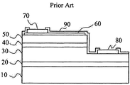
- FIG. 10 is a view illustrating another example of a conventional semiconductor light emitting device, wherein the semiconductor light emitting device is grown on a substrate 10 (eg, a sapphire substrate), a buffer layer 20 grown on the substrate 10, and a buffer layer 20.
- the p-side electrode 70, the p-type semiconductor layer 50, and the active layer 40 formed on the diffusion conductive layer 60 and the current diffusion conductive layer 60 are mesa-etched and exposed on the n-type semiconductor layer 30.
- the n-side electrode 80 and the protective film 90 formed are included.
- the current spreading conductive film 60 is provided so that the current is well supplied to the entire p-type semiconductor layer 50.
- the current spreading conductive film 60 is formed over almost the entire surface of the p-type semiconductor layer 50, and is formed of a transparent conductive film using, for example, ITO or Ni and Au, or a reflective conductive film using Ag. It can be formed as.
- the p-side electrode 70 and the n-side electrode 80 are metal electrodes for supplying current, for example, nickel, gold, silver, chromium, titanium, platinum, palladium, rhodium, iridium, aluminum, tin, indium , Tantalum, copper, cobalt, iron, ruthenium, zirconium, tungsten, molybdenum, or any combination thereof.
- the passivation layer 90 is formed of a material such as SiO 2 and may be omitted. As the semiconductor light emitting device becomes larger in size and consumes higher power, branch electrodes and a plurality of electrodes are introduced to smoothly spread current in the semiconductor light emitting device.
- branch electrodes are provided on the p-side electrode 70 and the n-side electrode 80, thereby spreading current.
- a plurality of p-side electrodes 70 and n-side electrodes 80 may be provided for sufficient current supply.
- Metal-like electrodes, such as the p-side electrode 70 and the n-side electrode 80 have a thick thickness and have a large light absorption loss, thereby reducing the light extraction efficiency of the light emitting device.
- the present disclosure provides a semiconductor light emitting device comprising: a plurality of semiconductor layers; A contact region in which the first semiconductor layer is exposed by partially removing the second semiconductor layer and the active layer; A non-conductive reflective film formed to cover the second semiconductor layer and the contact region so as to reflect light from the active layer to the side of the first semiconductor layer which is the growth substrate side; A branch electrode extending between the nonconductive reflecting film and the plurality of semiconductor layers; An electrical connection electrically connected to the branch electrode through the nonconductive reflecting film; And a direct connection type electrical connection electrically connected to the plurality of semiconductor layers through the non-conductive reflecting film.
- a first semiconductor layer having a first conductivity, a second semiconductor layer having a second conductivity different from the first conductivity, and a first semiconductor layer and a first A plurality of semiconductor layers interposed between the two semiconductor layers and having an active layer generating light through recombination of electrons and holes, the plurality of semiconductor layers sequentially grown using a growth substrate; A current diffusion conductive film positioned on the second semiconductor layer; A first electrode on the current spreading conductive film; And a current blocking layer interposed between the second semiconductor layer and the current spreading conductive film and positioned below the first electrode, wherein the current blocking layer has an inclined surface formed at an edge thereof. Is provided.
- a first semiconductor layer having a first conductivity, a second semiconductor layer having a second conductivity different from the first conductivity, and a first semiconductor layer sequentially grown using a growth substrate Preparing a plurality of semiconductor layers having an active layer interposed between the second semiconductor layers and generating light through recombination of electrons and holes; Forming a current blocking layer over the second semiconductor layer; An etching step is performed to form a mask to cover a certain area of the current blocking layer, to remove the current blocking layer in an area not covered by the mask, and to form an inclined surface at an edge of the remaining current blocking layer which is located below the edge of the mask. ; Forming a current spreading conductive film to cover the second semiconductor layer and the residual current blocking layer; And forming an electrode on the current spreading conductive film so as to be positioned above the residual current blocking layer.
- FIG. 1 is a view showing an example of a semiconductor light emitting device shown in US Patent No. 7,262,436,
- FIG. 2 is a view showing an example of a semiconductor light emitting device disclosed in Japanese Laid-Open Patent Publication No. 2006-120913;
- FIG. 3 is a view showing an example of a semiconductor light emitting device disclosed in Japanese Unexamined Patent Publication No. 2009-164423;
- FIG. 4 is a diagram illustrating an example of a semiconductor light emitting device according to the present disclosure.
- FIG. 5 is a cross-sectional view taken along the line A-A of FIG.
- FIG. 6 is a cross-sectional view taken along the line B-B of FIG.
- FIG. 7 is a diagram illustrating a state in which a p-side electrode, an n-side electrode, and a non-conductive reflective film are removed from the semiconductor light emitting device of FIG. 4;
- FIG. 8 illustrates another example of a semiconductor light emitting device according to the present disclosure
- FIG. 9 illustrates another example of a semiconductor light emitting device according to the present disclosure.
- FIG. 10 is a view showing an example of a conventional semiconductor light emitting device
- FIG. 11 is a diagram illustrating an example of a semiconductor light emitting device according to the present disclosure.
- FIG. 12 is a cross-sectional view taken along the line A-A of FIG. 11;
- 13 is a graph showing a simulation result showing the relationship between the thickness of the current blocking layer and the reflectance
- FIG 17 illustrates another example of the semiconductor light emitting device according to the present disclosure.
- FIG. 18 is a view showing still another example of a semiconductor light emitting device according to the present disclosure.
- FIG 19 illustrates another example of the semiconductor light emitting device according to the present disclosure.
- FIG. 4 is a diagram illustrating an example of a semiconductor light emitting device according to the present disclosure
- FIG. 5 is a cross-sectional view taken along line AA of FIG. 4
- FIG. 6 is a cross-sectional view taken along line BB of FIG. 4
- FIG. 4 is a diagram showing a state in which the p-side electrode, the n-side electrode, and the non-conductive reflecting film are removed from the semiconductor light emitting device of FIG.
- the semiconductor light emitting device 1 may have a planar shape having a substantially rectangular shape, and in the following description, for convenience of description, the first side 101 may have a short side positioned on the left side of the semiconductor light emitting device 1 shown in FIG. 4. ), And the short side opposite to the first side 101 is defined as the second side 102.
- the semiconductor light emitting device 1 is grown on the substrate 10, the buffer layer 20 grown on the substrate 10, the n-type semiconductor layer 30 grown on the buffer layer 20, and the n-type semiconductor layer 30. And an active layer 40 generating light through recombination of holes and a p-type semiconductor layer 50 grown on the active layer 40.
- the semiconductor light emitting device 1 also partially removes the p-type semiconductor layer 50 and the active layer 40 to emit light from the contact region 35 and the active layer 40 where the n-type semiconductor layer 30 is exposed.
- a p-side electrode 92 formed on the side of the first side 101 to supply one of electrons and holes to the p-type semiconductor layer 50, and on the side of the second side 102 above the non-conductive reflective film 91.
- the n-side electrode 80 is formed apart from the p-side electrode 92 to supply the other of electrons and holes to the n-type semiconductor layer 30 through the contact region 35.
- the substrate 10 is mainly used as the substrate 10, and the substrate 10 may be finally removed, and the buffer layer 20 may be omitted.
- the n-side electrode 80 may be formed on the n-type semiconductor layer 30 side or the conductive substrate 10 side from which the substrate 10 is removed.
- the positions of the n-type semiconductor layer 30 and the p-type semiconductor layer 50 may be changed, and are mainly made of GaN in the group III nitride semiconductor light emitting device.
- Each semiconductor layer 20, 30, 40, 50 may be composed of multiple layers, and additional layers may be provided.
- Three p-side branch electrodes 93 are provided between the p-type semiconductor layer 50 and the nonconductive reflecting film 91.
- the p-side branch electrode 93 may extend from the bottom of the region adjacent to the n-side electrode 80 of the p-side electrode 92 in the direction of the n-side electrode 80 and may extend to the bottom of the n-side electrode 80. have. That is, the p-side branch electrode 93 extends in the direction of the second side 102 from the first side 101 side of the semiconductor light emitting element.
- the p-side branch electrode 93 is preferably formed as long as possible.
- the p-side branch electrode 93 may also be divided into an elongated branch portion 98 and a connection portion 99 having a wide width.
- the connecting portion 99 is positioned at the end of the first side 101 of the p-side branch electrode 93 positioned below the region adjacent to the n-side electrode 80 of the p-side electrode 92.
- the number of p-side branch electrodes 93 is not limited to three, but may be provided in one or more various numbers.
- a p-side electrical connection 94 for electrically connecting the p-side branch electrode 93 and the p-side electrode 92 is provided.
- the p-side electrical connection 94 penetrates the non-conductive reflecting film 91 at the lower portion of the region adjacent to the n-side electrode 80 of the p-side electrode 92, that is, at the connection portion 99 of the p-side branch electrode 93. It is formed to.
- a p-side direct connection type electrical connection 104 directly connecting the p-type semiconductor layer 50 and the p-side electrode 92 is provided.
- the p-side direct connection type electrical connection 104 has a lower portion of the p-side electrode 92 farther from the n-side electrode 80 than the p-side electrical connection 94, that is, the lower portion of the region adjacent to the first side 101. Is formed to penetrate the non-conductive reflecting film (91).
- FIGS. 4 and 7 show an embodiment in which three p-side electrical connections 94 and three p-side direct-connect electrical connections 104 are provided, their numbers may vary and may differ from one another. .
- the support electrode having a relatively wide width in the lower portion of the p-side direct-connected electrical connection 104 may be provided.
- the supporting electrode 106 may be formed together with the p-side branch electrode 93 before the formation of the non-conductive reflective film 91.
- the supporting electrode 106 is not essential and may be omitted.
- the contact region 35 partially removes the p-type semiconductor layer 50 and the active layer 40 through a mesa etching process to expose the n-type semiconductor layer 30. Is formed.
- the contact area 35 may comprise a linear contact area 31 and a pointed contact area 33.
- the linear contact region 31 extends from the bottom of the region adjacent to the p-side electrode 92 of the n-side electrode 80 in the direction of the p-side electrode, and may extend to the bottom of the p-side electrode 92.
- the pointed contact region 33 is located below the linear contact region 31 and is located below the region adjacent to the second side 102 of the n-side electrode 80, which is far from the p-side electrode 92. .
- Two linear contact zones 31 and two pointed contact zones 33 are provided, with the two linear contact zones 31 being parallel with the p-side branch electrodes 92 between the p-side branch electrodes 92. Is extended.
- the linear contact region 31 and the point contact region 33 may be open in the lateral direction of the semiconductor light emitting element, but not open to either side and the periphery of the linear contact region 31 and the p-type semiconductor layer 50. It may be surrounded and blocked.
- FIGS. 4 and 7 show an embodiment in which two linear contact areas 31 and two pointed contact areas 33 are provided, their numbers may vary and may differ from one another. The arrangement of the linear contact zones 31 and the pointed contact zones 33 may also vary.
- An n-side branch electrode 81 is provided between the n-type semiconductor layer 30 and the non-conductive reflecting film 91 inside each linear contact region 31.
- the n-side branch electrode 81 extends from the bottom of the n-side electrode 80 along the linear contact region 31 toward the p-side electrode 92.
- the n-side branch electrode 81 may extend from the lower portion of the n-side electrode 80 adjacent to the p-side electrode 92 in the direction of the p-side electrode 92 and may extend to the lower portion of the p-side electrode 92. have. That is, the n-side branch electrode 81 extends in the direction of the first side 101 from the second side 102 side of the semiconductor light emitting device.
- the n-side branch electrode 80 may also be divided into an elongated branch 88 and a wide width connecting portion 89.
- the connecting portion 89 is positioned at an end portion of the n-side electrode 80 at the second side 102 side of the n-side branch electrode 81 positioned below the region adjacent to the p-side electrode 92.
- the linear contact region 31 is formed in a narrow width at the portion where the branch portion 88 of the n-side branch electrode 81 is positioned, and the connection portion 89 of the n-side branch electrode 81 is located. It can be formed in a wide width at the portion.
- n-side electrical connection 82 for electrically connecting the n-side branch electrode 81 and the n-side electrode 80 is provided.
- the n-side electrical connection 82 penetrates the non-conductive reflecting film 91 at the lower portion of the n-side electrode 80 adjacent to the p-side electrode 92, that is, at the connection portion 89 of the n-side branch electrode 81. It is formed to.
- an n-side direct connection type electrical connection 112 is provided that directly connects the n-type semiconductor layer 30 and the n-side electrode 80 inside the pointed contact region 33.
- the n-side direct connection type electrical connection 112 is a lower portion of the n-side electrode 80 that is farther from the p-side electrode 92 than the n-side electrical connection 82, that is, the lower portion of the region adjacent to the second side 101. Is formed to penetrate the non-conductive reflecting film (91).
- the n-side electrical connection 82 and the n-side direct-connected electrical connection 112 correspond to the number of linear contact areas 31 and the point contact areas 33.
- the support electrode having a relatively wide width in the lower portion of the n-side direct-connected electrical connection 112 may be provided.
- the supporting electrode 114 may be formed together with the n-side branch electrode 81 before the formation of the non-conductive reflective film 91.
- the supporting electrode 114 is not essential and may be omitted.
- the area under the p-side electrode 92 is mainly The p-side branch electrode 93 and the p-side electrode 92 supply current through the p-side direct-connected electrical connection 104, and the region under the n-side electrode 80 extends below the n-side electrode 80. And a current is supplied through the p-side electrical connection 94 which electrically connects the p-side branch electrode 93 to each other.
- the region where the p-side direct connection electrical connection 104 can be formed is the n-side electrode 80 through which the p-side direct connection electrical connection 104 can not be formed. And the region between the n-side electrode 80 and the p-side electrode 92 supplies current through the p-side branch electrode 93 and the p-side electrical connection 94. Similarly, in order to supply current to the n-type semiconductor layer 30 positioned below the non-conductive reflecting film 91, the region under the n-side electrode 80 mainly draws current through the n-side direct-connected electrical connection 112.
- Current is supplied via the n-side electrical connection 82. That is, the region capable of forming the n-side direct-connected electrical connection 112 is the p-side electrode 92 which cannot form the n-side direct-connected electrical connection 112 through the n-side direct-connected electrical connection 112. And the region between the n-side electrode 80 and the p-side electrode 92 supplies current through the n-side branch electrode 81 and the n-side electrical connection 82.
- the branch electrodes 81 and 93 do not depend entirely on the electrode 80, 92
- the area below allows for efficient current supply and diffusion using direct-connected electrical connections 112 and 104. That is, as the n-side branch electrode 81 does not extend to the region under the n-side electrode 80, and the p-side branch electrode 93 does not extend to the region under the p-side electrode 92, it is relatively small.
- the branch electrodes 81 and 93 can be short. For this reason, light absorption by a branch electrode can be reduced and light extraction efficiency can be improved.
- the combination of the n-side branch electrode 81 and the n-side electrical connection 82 is omitted or the n-side Direct connection electrical connection 112 may be omitted.
- p-side branch electrode 93 and n-side branch electrode 81 2um-3um are suitable. Too thin a thickness may cause an increase in operating voltage, and too thick a branch electrode may cause process stability and a material cost increase.
- a light absorption prevention film (on the p-type semiconductor layer 50 corresponding to the p-side branch electrode 93 and the p-side direct-connected electrical connection 104, respectively) 95) can be formed prior to the formation of the p-side branch electrode 93.
- the light absorption prevention film 95 is formed in a slightly wider width than the p-side branch electrode 93 and the p-side direct connection type electrical connection 104.
- the light absorption prevention layer 95 prevents light generated in the active layer 40 from being absorbed by the p-side branch electrode 93 and the p-side direct-connected electrical connection 104.
- the light absorption prevention film 95 may have only a function of reflecting some or all of the light generated in the active layer 40, and the current from the p-side branch electrode 93 and the p-side direct-connected electrical connection 104 is p-sided. It may have only a function of preventing the branch electrode 93 and the p-side direct-connected electrical connection 104 from flowing directly below, or may have both functions.
- the light absorption prevention film 95 is a single layer (e.g. SiO 2 ) or a multilayer (e.g. Si0 2 / TiO 2 / SiO 2 ) made of a light-transmissive material having a lower refractive index than the p-type semiconductor layer 50.
- the light absorption prevention layer 95 may be made of a non-conductive material (eg, a dielectric material such as SiO x or TiO x ).
- the thickness of the light absorption prevention film 95 is appropriately 0.2um to 3.0um depending on the structure. If the thickness of the light absorption prevention film 95 is too thin, the function is weak. If the thickness is too thick, deposition of the transparent conductive film 60 formed on the light absorption prevention film 95 may be difficult.
- the light absorption prevention film 95 does not necessarily need to be made of a light transmissive material, nor is it necessarily necessarily made of a non-conductive material. However, by using the transparent dielectric material, the effect can be further enhanced.
- the transmissive conductive film 60 may be formed on the p-type semiconductor layer 50 before the p-side branch electrode 93 is formed following the formation of the light absorption prevention film 95.
- the transparent conductive film 60 is formed to cover almost the entirety of the p-type semiconductor layer 50 except for the contact region 35 formed through the mesa etching process. Therefore, the light absorption prevention film 95 is disposed between the transparent conductive film 60 and the p-type semiconductor layer 50.
- the current spreading ability is inferior, and in the case where the p-type semiconductor layer 50 is made of GaN, most of the transparent conductive film 60 should be assisted.
- materials such as ITO and Ni / Au may be used as the transparent conductive film 60.
- the p-side branch electrode 93 is formed on the transparent conductive film 60 on which the light absorption prevention film 95 is located, and the n-side branch electrode 81 is formed in the contact region 35. ) Will be formed.
- the non-conductive reflecting film 91 is a contact region 35 and n including a linear contact region 31 and a pointed contact region 33 after the n-side branch electrode 81 and the p-side branch electrode 93 are formed.
- the p-type semiconductor layer 50 including the side branch electrodes 81 and the p side branch electrodes 93 is formed to be covered as a whole.
- the nonconductive reflecting film 91 reflects light from the active layer 40 to the n-type semiconductor layer 30 when the substrate 10 used for growth or the substrate 10 is removed.
- the non-conductive reflective film 91 preferably also covers the exposed surfaces of the p-type semiconductor layer 50 and the active layer 40 that connect the top surface of the p-type semiconductor layer 50 and the top surface of the contact region 35.
- the non-conductive reflective film 91 does not necessarily cover all regions on the n-type semiconductor layer 30 and the p-type semiconductor layer 50 exposed by etching on the opposite side of the substrate 10. Should be placed in.
- the n-type semiconductor layer 30, that is, the contact region 35, exposed through etching may not be covered with the non-conductive reflective film 91.
- the non-conductive reflecting film 91 functions as a reflecting film but is preferably made of a light transmitting material to prevent absorption of light.
- the non-conductive reflecting film 91 may be formed of a light transmitting dielectric material such as SiO x , TiO x , Ta 2 O 5 , and MgF 2 . Can be configured.
- the non-conductive reflecting film 91 is a single dielectric film composed of a transparent dielectric material such as SiO x , for example, a single distributed Bragg reflector made of a combination of SiO 2 and TiO 2 , a plurality of heterogeneous dielectric films or dielectrics.
- the dielectric film has a lower refractive index than the p-type semiconductor layer 50 (eg, GaN), it is possible to partially reflect light above the critical angle to the substrate 10 side, and the distribution Bragg reflector transmits a larger amount of light to the substrate 10. It can be reflected to the side and can be designed for a specific wavelength can be effectively reflected in response to the wavelength of light generated.
- the p-type semiconductor layer 50 eg, GaN
- the non-conductive reflecting film 91 has a double structure of the distribution Bragg reflector 91a and the dielectric film 91b.
- the dielectric film 91b having a predetermined thickness can be formed, whereby the distributed Bragg reflector 91a can be stably manufactured and can also help to reflect light. have.
- the semiconductor light emitting device there is a step in mesa etching for forming the n-side contact region 31, and the step such as the p-side branch electrode 93 or the n-side branch electrode 81. And a process for punching the non-conductive reflecting film 91 as described in detail below even after the non-conductive reflecting film 91 is formed, thus forming the dielectric film 91b. Especially when you need to be careful.
- the material of the dielectric film 91b is suitably SiO 2 , and the thickness thereof is preferably 0.2 ⁇ m to 1.0 ⁇ m. If the thickness of the dielectric film 91b is too thin, it may be insufficient to sufficiently cover the n-side branch electrode 81 and the p-side branch electrode 93 having a height of about 2 ⁇ m to 3 ⁇ m. This can be a burden on the hole forming process. The thickness of the dielectric film 91b may then be thicker than the thickness of the subsequent distribution Bragg deflector 91a. In addition, it is necessary to form the dielectric film 91b in a manner more suitable for securing device reliability.
- the dielectric film 91b made of SiO 2 is preferably formed by Chemical Vapor Deposition (CVD), and particularly, Plasma Enhanced CVD (PECVD).
- CVD Chemical Vapor Deposition
- PECVD Plasma Enhanced CVD
- PVD Physical Vapor Deposition
- the dielectric film 91b when the dielectric film 91b is formed by E-Beam Evaporation, the inclined surface formed by the side or mesa etching of the p-side branch electrode 93 and the n-side branch electrode 81 having a step difference may be formed.
- the dielectric film 91b is thinly formed on the stepped surface or the like, and when the dielectric film 91b is thinly formed on the stepped surface, the p-side branch electrode 93 and the n-side branch electrode 81 are formed on the p-side electrode.
- a short may occur between the electrodes, so that the dielectric film 91b is preferably formed by chemical vapor deposition for reliable insulation. Therefore, it is possible to secure the function as the non-conductive reflective film 91 while securing the reliability of the semiconductor light emitting element.
- the distribution Bragg reflector 91a is formed on the dielectric film 91b to form the non-conductive reflecting film 91 together with the dielectric film 91b.
- the distribution Bragg reflector 91a of a repeating laminated structure composed of a combination of TiO 2 / SiO 2 is physical vapor deposition (PVD), and among them, electron beam evaporation or sputtering. Or by thermal evaporation.
- each layer is designed to basically have an optical thickness of 1/4 of a given wavelength, but the angle of incidence of light Optimal design considering the effect of light and wavelengths of light (blue, green, yellow, red, etc.) that can occur in the package does not require that the optical thickness of each layer is exactly 1/4, and the number of combinations is 4 ⁇ 20 pairs are suitable. This is because if the number of combinations is too small, the reflection efficiency of the distributed Bragg reflector is reduced, and if the number of combinations is too large, the thickness becomes excessively thick.
- each layer is basically designed to have an optical thickness of 1/4 of a given wavelength, but may be designed to have an optical thickness greater than 1/4 of a given wavelength, depending on the wavelength band under consideration.
- the distributed Bragg reflector 91a may be designed with combinations of TiO 2 layers / SiO 2 layers having different optical thicknesses.
- the distribution Bragg reflector 91a may include a combination of a plurality of TiO 2 layers / SiO 2 layers that are repeatedly stacked, and the combination of the plurality of TiO 2 layers / SiO 2 layers may have different optical thicknesses, respectively. have.
- the non-conductive reflecting film 91 Due to the formation of the non-conductive reflecting film 91, the p-side branch electrode 93 and the n-side branch electrode 81 are completely covered by the non-conductive reflecting film 91.
- the non-conductive reflecting film 91 is formed. A hole is formed, and electrical connections 94 and 82 of the structure filled with electrode material are formed in the hole.
- the p-side electrode 92 and the n-side electrode 80 in direct communication with the light-transmissive conductive film 60 and the n-type semiconductor layer 30, respectively.
- a hole in the form is formed, and direct connection electrical connections 104 and 112 of the structure filled with electrode material are formed in the hole.
- Such holes are preferably formed by dry etching or wet etching, or a combination of both. Since the branch portions 98 and 88 of each of the p-side branch electrode 93 and the n-side branch electrode 81 are formed in a narrow width, the electrical connections 94 and 82 are connected to the p-side branch electrode 93 and the n-side. It is preferable to be positioned above the connecting portions 99 and 89 of each of the branch electrodes 81.
- the p-side electrode 92 and the n-side electrode 80 are formed on the non-conductive reflecting film 91 following the formation of the electrical connections 94 and 82.
- the p-side electrode 92 and the n-side electrode 80 cover all or almost all of the non-conductive reflecting film 91 in view of helping to reflect light from the active layer 40 toward the substrate 10 side. It can be formed over a large area, and serves as a conductive reflective film.
- the p-side electrode 92 and the n-side electrode 80 are preferably spaced apart from each other on the non-conductive reflective film 91 in order to prevent a short circuit. Therefore, the p-side electrode 92 is disposed on the non-conductive reflective film 91.
- the p-side electrode 92 and the n-side electrode 80 may be formed over the same area on the non-conductive reflecting film 91 or may have different areas.
- the p-side electrode 92 is larger than the n-side electrode 80 in the extending direction of the branch electrodes 81 and 93. It can be formed to have a wider width.
- the n-side electrode 80 may be formed in the contact region 35 therein without being formed over a large area.
- Al As the material of the p-side electrode 92 and the n-side electrode 80, Al, Ag and the like having good reflectance are suitable, but for stable electrical contact, Al is combined with materials such as Cr, Ti, Ni, Au, or alloys thereof. Highly reflective metals such as, Ag and the like are preferably used.
- the p-side electrode 92 and the n-side electrode 80 serve to supply current to the p-side branch electrode 93 and the n-side branch electrode 81, to connect the semiconductor light emitting device to an external device, and It is formed over a large area to perform the function of reflecting light from the active layer 40 and / or heat radiation function.
- the p-side electrode 92 and the n-side electrode 80 are both formed on the non-conductive reflecting film 91 as described above, the height difference between the p-side electrode 92 side and the n-side electrode 80 side is minimized.
- the semiconductor light emitting device according to the present disclosure has an advantage when coupled to a mounting portion (eg, PCB, submount, package, COB).
- the p-side electrode 92 and the n-side electrode 80 may not be included in the semiconductor light emitting device, but may be formed on the mounting portion on which the semiconductor light emitting device is installed.
- the p-side branch electrode 93 and the n-side branch to be placed below the non-conductive reflecting film 91 the p-side branch electrode 93 and the n-side branch to be placed below the non-conductive reflecting film 91
- the p-side branch electrode 93 extends long under the n-side electrode 80 placed on the non-conductive reflective film 91
- the n-side branch electrode 81 extends the non-conductive reflective film 91.
- the electrodes 92 and 80 and the branch are formed. Short circuits between the electrodes 93 and 81 are prevented.
- the p-side branch electrode 93 and the n-side branch electrode 81 as described above, it is possible to supply a current to the semiconductor layer region that is required without restriction in forming a flip chip.
- the p-side electrode 92, the n-side electrode 80, the p-side branch electrode 93 and the n-side branch electrode 81 are composed of a plurality of metal layers.
- the lowermost layer should have a high bonding strength with the transparent conductive film 60, and materials such as Cr and Ti may be mainly used, and Ni, Ti, TiW, and the like may also be used.
- materials such as Cr and Ti may be mainly used, and Ni, Ti, TiW, and the like may also be used.
- Al, Ag and the like having good reflectance can also be used for the p-side branch electrode 93 and the n-side branch electrode 81.
- Au is used for wire bonding or connection with an external electrode.
- Au is used for wire bonding or connection with an external electrode.
- Au may be used to connect with the external electrode, but other metals may be used according to the bonding technique.
- Sn, Ni, Ti, Pt, W, TiW, Cu or alloys thereof may be used, but is not limited thereto.
- Ni, Ti, TiW, W, or the like is used between the lowermost layer and the uppermost layer, or Al, Ag, or the like is used when a high reflectance is required.
- Au since the p-side branch electrode 93 and the n-side branch electrode 81 must be electrically connected to the electrical connections 94 and 82, Au may be considered as the uppermost layer.
- the inventors have found that it is inappropriate to use Au as the uppermost layer of the p-side branch electrode 93 and the n-side branch electrode 81.
- the non-conductive reflective film 91 is deposited on Au, there is a problem in that the bonding force between the two is weak and easily peeled off.
- the uppermost layer of the branch electrode is made of a material such as Ni, Ti, W, TiW, Cr, Pd, Mo instead of Au, the adhesion to the non-conductive reflective film 91 to be deposited thereon is maintained. Reliability can be improved.
- the above metal serves as a diffusion barrier to help secure the stability of the subsequent processes and the electrical connections 94 and 82. Becomes
- FIG 8 illustrates another example of the semiconductor light emitting device according to the present disclosure.
- the p-side branch electrode 93 has an extended branch 96 extending further inclined with the branch 98 under the n-side electrode 80.
- the extending branch 96 preferably extends into the area between the linear contacting zone 31 and the pointed connection zone 33.
- the extended branch 96 may extend in the middle of the branch 98 as shown in FIG. 8, but may also extend at the end side of the second side 102 of the branch 98.
- the extended branch 96 may extend in a direction perpendicular to the branch 98 as shown in FIG. 8, but may extend in a direction of another angle.
- the extended branch 96 may also extend in one direction orthogonal to the branch 98 as shown in FIG. 8, but may extend in both directions. Further, as shown in FIG. 8, only a part of the plurality of p-side branch electrodes 93 may include the extension branch 96, and all of the p-side branch electrodes 93 may include the extension branch 96. have.
- the n-side branch electrode 81 also includes an extended branch portion 87 extending further inclined with the branch portion 88 below the p-side electrode 92.
- the extending branch 87 preferably extends into the region between the p-side electrical connection 94 and the p-side direct-connected electrical connection 104.
- the linear contact region 31 has an additional extended contact region 32 which extends further along the area in which the extended branch 87 is to be placed. You will have to.
- the extended branch portion 87 may extend in the middle of the branch portion 88 as shown in FIG. 8, but may also extend at the end side of the first side 101 of the branch portion 88.
- the extended branch 87 may extend in a direction perpendicular to the branch 88 as shown in FIG. 8, but may extend in a direction of another angle.
- the extended branch 87 may also extend on both sides with respect to the branch 88 as shown in FIG. 8, but may extend only on one side.
- all of the plurality of n-side branch electrodes 81 may include the extension branch 87, and only some n-side branch electrodes 81 may include the extension branch 87. have.
- the p-side direct connection type electrical connection 104 may be provided in a larger number than the p-side branch electrode 93, as shown in Figure 8 may be provided in a smaller number on the contrary.
- the p-side direct-connected electrical connection 104 is not necessarily arranged in a line.
- FIG 9 is a view illustrating still another example of the semiconductor light emitting device according to the present disclosure.
- the extension branches 96 provided in the plurality of p-side branch electrodes 93 may be connected to each other under the n-side electrode 80.
- the extension branches 96 may be connected to each other.
- extension branches 87 provided in the plurality of n-side branch electrodes 81 may also be connected to each other under the p-side electrode 92.
- the additional extended contact zones 32 provided in the plurality of linear contact zones 31 will also have to be connected to each other.
- the length of all p side branch electrodes 93 does not necessarily need to be the same.
- the n-side direct connection type electrical connection 112 may be provided in a smaller number than the n-side branch electrode 81, or vice versa.
- FIG. 11 is a diagram illustrating an example of a semiconductor light emitting device according to the present disclosure
- FIG. 12 is a cross-sectional view taken along line A-A of FIG. 11.
- the semiconductor light emitting device 100 may include a substrate 110, a buffer layer 120, a first semiconductor layer 130, an active layer 140, a second semiconductor layer 150, and current blocking.
- the layer 160, the current spreading conductive layer 170, the first electrode 180, and the second electrode 190 are included.
- 2 semiconductor layers 150 are sequentially formed.
- the current diffusion conductive layer 170 is positioned on the second semiconductor layer 150, and the first electrode 180 is positioned on the current diffusion conductive layer 170.
- the current blocking layer 160 is positioned under the first electrode 180 between the second semiconductor layer 150 and the current spreading conductive layer 170. That is, the current blocking layer 160 is provided on the second semiconductor layer 150, and the current spreading conductive film 170 is provided to cover the current blocking layer 160 and the second semiconductor layer 150.
- the semiconductor layers epitaxially grown on the substrate 110 are mainly grown by organometallic vapor phase growth (MOCVD), and each layer may further include sublayers as necessary.
- MOCVD organometallic vapor phase growth
- the substrate 110 a GaN-based substrate is used as the homogeneous substrate, and a sapphire substrate, a SiC substrate, or a Si substrate is used as the heterogeneous substrate. Any substrate may be used as long as the group III nitride semiconductor layer can be grown.
- the substrate 110 may be finally removed, and the buffer layer 120 may be omitted.
- the second electrode 190 may be formed on the first semiconductor layer 130 side from which the substrate 110 has been removed or on the substrate 110 side having conductivity.
- the first semiconductor layer 130 and the second semiconductor layer 150 are provided to have different conductivity.
- the first semiconductor layer 130 may be an n-type semiconductor layer 130 (eg, an n-type GaN layer), and the second semiconductor layer 150 may be a p-type semiconductor layer 150 (eg, p-type GaN). Layer), and vice versa.
- the first semiconductor layer is etched by etching the second semiconductor layer 150 and the active layer 140 in the form of mesas. Let 130 be exposed.
- a dry etching method for example, an inductively coupled plasma (ICP) may be used.
- ICP inductively coupled plasma
- the second electrode 190 is positioned on the exposed first semiconductor layer 130.
- the current blocking layer 160 may be made of an insulator, and a material in which the current blocking layer 160 is in contact, that is, a transparent dielectric material having a lower refractive index than the first semiconductor layer 150 (for example, a P-type GaN layer) in this embodiment. It is preferable to form.
- the current blocking layer 160 may be formed of, for example, at least one selected from the group consisting of SiO x , TiO x , Ta 2 O 5 , MgF 2 , SiN, SiON, Al 2 O 3 , AlO x, and NiO x . Meanwhile, the current blocking layer 160 may include a distributed bragg reflector (DBR).
- DBR distributed bragg reflector
- the current blocking layer 160 may include a single dielectric film composed of a transparent dielectric material such as SiO x and TiO x , or a plurality of heterogeneous dielectric films having different refractive indices (eg, SiO 2 / TiO 2 , SiO 2 / Ta). 2 O 5 , SiO 2 / TiO 2 / Ta 2 O 5, etc., or a distributed Bragg reflector consisting of, for example, a combination of SiO 2 / TiO 2 or SiO 2 / Ta 2 O 5 . : DBR) can be made of various structures, such as alone or in combination of the dielectric film and the distribution Bragg reflector described above.
- a transparent dielectric material such as SiO x and TiO x
- a plurality of heterogeneous dielectric films having different refractive indices eg, SiO 2 / TiO 2 , SiO 2 / Ta.
- 2 O 5 SiO 2 / TiO 2 / Ta 2 O 5, etc.
- each layer can be designed to have a reflectivity of 90% or more in the LED wavelength band.
- the current blocking layer 160 is made of the distribution Bragg reflector alone
- the distribution Bragg reflector is made of a relatively large number of combinations, and when the current blocking layer 160 is made of a combination of the distribution Bragg reflector and a dielectric film such as SiO 2 Bragg reflectors may be made in a relatively small number of combinations.
- the current blocking layer 160 includes the distributed Bragg reflector, even if the current blocking layer 160 is configured to have a relatively thin thickness, the light absorption prevention function can be effectively performed.
- the current spreading conductive film 170 has a light transmitting property and improves the uniformity of light.
- the current spreading conductive film 170 is mainly formed of an ITO or Ni / Au oxide film. Even when the current diffusion conductive film 170 is made of the most common ITO, it is preferable to form a thin layer because it absorbs a part of the light generated from the active layer 140. If the current diffusion conductive film 170 is too thin, it is preferable that the current diffusion conductive film is excessively thin. Not. Therefore, in order to minimize the absorption of the generated light while being able to perform a smooth current spreading function without increasing the operating voltage, the current spreading conductive film 170 is formed to have a thin thickness within the range of 200 kHz to 1000 kHz.
- the current blocking layer 160 Since the current blocking layer 160 is made of an insulator, the current blocking layer 160 has a high resistance to block a current flowing to the active layer 140 in a portion located below the first electrode 180, and thus the first electrode 180. There is an advantage that can reduce the loss of light by. At this time, the current is diffused through the current diffusion conductive film 170. Meanwhile, the current blocking layer 160 also performs a function of preventing light absorption by the first electrode 180. As the current blocking layer 160 is formed of a material having a lower refractive index than the material forming the second semiconductor layer 150, the light generated from the active layer 140 is emitted from the second semiconductor layer 150 and the current blocking layer 160. Reflected at the interface of the has the advantage of reducing the absorption of light by the first electrode (180).
- the critical angle is determined by the difference in refractive index between the second semiconductor layer 150 and the current blocking layer 160. Light entering the critical angle is reflected only a certain amount at the interface, and light entering at an angle larger than the critical angle is totally reflected. Therefore, the amount of light absorbed by the first electrode 180 can be reduced.
- the thickness of the medium must be at least as thick as the wavelength of light. Accordingly, the refractive index of P-type GaN constituting the second semiconductor layer 150 is about 2.4, the refractive index of SiO 2 constituting the current blocking layer 160 is about 1.5, and the refractive index of ITO constituting the current diffusion conductive film 170.
- the thickness T of the current blocking layer 160 is sufficiently thick, and the greater the reflectance between the first semiconductor layer 150 and the current blocking layer 160, the better the external quantum efficiency.
- the current blocking layer 160 is formed in an island shape under the first electrode 180.
- the width of the current blocking layer 160 is excessively wide, the area where the current is cut off may become too large, and the efficiency of the device may be reduced. Also, light generated by the active layer 140 and incident on the current blocking layer 160 is more than necessary. If the current blocking layer 160 is narrow, the width of the current blocking layer 160 may not be effectively reflected to the first electrode 180. It is preferable that the width of the first electrode 18 be equal to or slightly wider.
- FIG. 13 is a graph illustrating a simulation result indicating a relationship between a thickness of a current blocking layer and a reflectance.
- the horizontal axis represents an incident angle of light incident on the current blocking layer 160
- the vertical axis represents a reflectance.
- the current blocking layer 160 is made of SiO 2 and simulated by changing the thickness, and a graph simulating the case where the thicknesses are 2500 mW and 3000 mW is typically shown.
- the incident angle is very small or large, it can be seen that the reflectance does not have a large difference depending on the thickness T of the current blocking layer 160.
- the reflectance varies greatly depending on the thickness T of the current blocking layer 160.
- the thickness T of the current blocking layer 160 is different.
- the thickness is less than 3000 mW, the reflectance decreases drastically, and when the thickness T of the current blocking layer 160 is 3000 mW or more, it can be seen that it has a high reflectance regardless of the incident angle. Therefore, the thickness T of the current blocking layer 160 may affect the reflection efficiency of light, and in order to effectively reflect the light, the current blocking layer 160 preferably has a thickness of 3000 ⁇ or more.
- the current blocking layer 160 also has an inclined surface 165 formed at the edge.
- the inclined surface 165 of the current blocking layer 160 preferably has a gentle inclination ⁇ of 45 degrees or less with respect to the upper surface of the second semiconductor layer 150.
- the inclined surface 165 having a gentle inclination ⁇ of 45 ° or less is formed. Can be.
- the side surface of the current blocking layer 160 is formed as the inclined surface 165, it is possible to prevent damage to the current spreading conductive layer 170.
- the current blocking layer 160 is Since the thick and the current spreading conductive film 170 is formed significantly thinner than this, there is a possibility that damage such as local break in the current spreading conductive film 170 may occur.
- the side of the current blocking layer 160 is formed in a vertical plane or a slope close to the vertical, so that the slope of the current diffusion conductive film 170 changes sharply (for example, the corner portion where the side and the upper surface of the current blocking layer intersects).
- the current diffusion conductive film 170 is more likely to be damaged due to non-uniform expansion caused by the difference in thermal expansion coefficient.
- the inclination change of the current diffusion conductive film 170 is alleviated by the slope of the current blocking layer 160 having a gentle inclined surface 165 at the edge thereof, whereby the current diffusion conductive film according to the thermal expansion coefficient difference is reduced. Damage to the 170 may be prevented, and therefore, an increase in the operating voltage due to the damage of the current spreading conductive layer 170 may also be prevented.
- Such a current blocking layer 160 is, for example, plasma enhanced chemical vapor deposition (PECVD), low pressure chemical vapor deposition (LPCVD), sputtering, electron beam deposition (E-beam) on the second semiconductor layer. It is formed by depositing by evaporation, thermal evaportation, etc. and then removing unnecessary parts. For example, the process of removing the unnecessary portion may be performed by wet etching, and in this process, the current blocking layer 160 may include an inclined surface 165 formed at an edge thereof.
- PECVD plasma enhanced chemical vapor deposition
- LPCVD low pressure chemical vapor deposition
- E-beam electron beam deposition
- FIG. 14 to 16 are views showing a method of forming a current blocking layer having an inclined surface.
- the current blocking layer 160 ′ is first formed to cover the second semiconductor layer 150.
- the current blocking layer 160 ′ is divided into a region a to remain and a region b to be removed, and a mask 163 is formed to cover the region a to remain.
- the mask 163 may be made of photoresist.
- wet etching is performed to remove the current blocking layer b of the region to be removed, which is not covered with the mask 163, as shown in FIG. 15. Thereafter, as shown in FIG.
- the mask 163 is removed to leave only the current blocking layer a of the region to be left on the second semiconductor layer 150.
- the inclined surface 165 is formed at the edge of the residual current blocking layer 160 positioned below the edge of the mask 163.
- the current blocking layer (a) of the region to remain to be located below the edge of the mask 163 The sides are gradually exposed to the etchant as it goes from top to bottom. Therefore, the etching liquid penetrates deeper horizontally in the upper portion of the current blocking layer (a) to be left during the etching process, and less etching liquid penetrates toward the lower portion.
- a method of weakening the adhesion between the photoresist used as the mask 163 and the SiO 2 layer forming the uppermost layer of the current blocking layer (a) may be used, in which case the etchant By infiltrating under this photoresist, an inclined surface 165 having a more gentle inclination can be obtained.
- the photoresist may be SiO 2 without the process using HMDS (Hexa Methyl Di Silazane, Si 2 (CH 3 ) 6 ), which is usually performed to increase the adhesion.
- HMDS Hexa Methyl Di Silazane, Si 2 (CH 3 ) 6
- a method of performing a wet etching process on a layer or maintaining the etchant temperature within a range of 30 ° C. to 50 ° C. higher than room temperature may be used.
- the current diffusion conductive film is formed to cover almost the entire surface of the second semiconductor layer 150 and the current blocking layer 150 by using a sputtering method, an electron beam deposition method, a thermal deposition method, or the like. 170) is formed.
- the current spreading conductive film 170 can be easily formed in good quality as the current blocking layer 160 has an inclined surface 165 of a gentle slope ⁇ at the edge. Specifically, when the side of the current blocking layer 160 is formed in a vertical plane or a slope close to the vertical, it is difficult to form a good quality current diffusion conductive film 170 on the side of the current blocking layer 160, and particularly good It is more difficult to form a thin current diffusion conductive film 170 of quality. However, as described above, since the current blocking layer 160 is formed to have an inclined surface having a gentle inclination at the edge, it is possible to easily form a thin current spreading conductive film 170 having good quality.
- the first electrode 180 and the second electrode 190 are formed by using a method such as a sputtering method, an electron beam evaporation method, a thermal evaporation method, or the like.
- the first electrode 180 and the second electrode 190 may be formed by stacking chromium, nickel, and gold.
- the second electrode 190 is formed on the first semiconductor layer 130 exposed by mesa etching, and the first electrode 180 is formed on the current diffusion conductive layer 170 on the current blocking layer 160.
- the first electrode 180 and the second electrode 190 may be located on opposite sides, and the present invention is not limited thereto, and the first electrode 180 and the second electrode 190 are not limited thereto.
- the shape and arrangement of the can be changed in various ways.
- FIG 17 illustrates another example of the semiconductor light emitting device according to the present disclosure.
- the semiconductor light emitting device 200 is substantially the same as the semiconductor light emitting device 100 described with reference to FIGS. 11 and 12 except that the semiconductor light emitting device 200 further includes a first branch electrode 285. Therefore, the same elements are given the corresponding reference numerals and duplicate descriptions are omitted.
- the semiconductor light emitting device 200 further includes a first branch electrode 285 extending from the first electrode 280 on the current spreading conductive film 270.
- the first branch electrode 285 helps smooth current spreading through good electrical contact with the current spreading conductive film 270.
- the current blocking layer 260 is formed between the second semiconductor layer 250 and the current diffusion conductive film 270. It extends below the first branch electrode 285 as well as the first electrode 280.
- the edge is formed of the inclined surface 265.
- FIG 18 illustrates another example of the semiconductor light emitting device according to the present disclosure.
- the semiconductor light emitting device 300 is substantially the same as the semiconductor light emitting device 200 described with reference to FIG. 17 except that the semiconductor light emitting device 300 further includes a non-conductive reflective film 375. Therefore, the same elements are given the corresponding reference numerals and duplicate descriptions are omitted.
- the semiconductor light emitting device 300 has a non-conductive reflective film 375 to have a flip chip shape.
- the non-conductive reflective film 375 has a first electrode 380, a first electrode on the second semiconductor layer 350 so as to reflect light from the active layer 340 to the first semiconductor layer 330 which is the growth substrate 310 side. It is formed to cover the branch electrode 385 and the current spreading conductive film 370.
- a first electrical connection 383 extending upwardly through the non-conductive reflecting film 375 is provided on the first electrode 380.
- a first pad electrode 387 is provided on the non-conductive reflective film 375 to be electrically connected to the first electrode 380 through the first electrical connection 383.
- the non-conductive reflective film 375 may also be formed on portions of the first semiconductor layer 330 and the second electrode 390 that are etched and exposed. Those skilled in the art should keep in mind that the non-conductive reflective film 375 does not necessarily cover all areas on the semiconductor layers 330 and 350 opposite the substrate 310.
- the non-conductive reflecting film 375 functions as a reflecting film, but is preferably made of a light transmitting material to prevent absorption of light.
- the non-conductive reflecting film 375 may be formed of a light transmitting dielectric material such as SiO x , TiO x , Ta 2 O 5 , and MgF 2 . Can be configured.
- the non-conductive reflective film 375 is made of SiO x , since the non-conductive reflective film 375 has a lower refractive index than the first semiconductor layer 350 (for example, P-type GaN), the light having a critical angle or more may be partially reflected toward the semiconductor layers 330, 340, and 350. do.
- the non-conductive reflecting film 375 is made of a distributed Bragg reflector (DBR: DBR made of a combination of SiO 2 and TiO 2 ), more light is reflected toward the semiconductor layers 130, 140, and 150. You can do it.
- the non-conductive reflecting film 375 has a double structure of a distribution Bragg reflector 375a and a dielectric film 375b having a lower refractive index than the first semiconductor layer 350.
- the dielectric film 375b having a predetermined thickness is formed so that the heterogeneous and heterogeneous deposits 350, 370, 380, 385, and 390 are present on the semiconductor layers 330, 340, and 350.
- the distribution Bragg reflector 375a can be manufactured stably, and can also help reflection of light.
- the material is suitably SiO 2 , and the thickness thereof is appropriately 0.2 ⁇ m to 1.0 ⁇ m.
- each layer is designed to have an optical thickness of 1/4 of a given wavelength when composed of TiO 2 / SiO 2 , with a suitable number of combinations of 4 to 20 pairs. Do.
- the first pad electrode 387 has a non-conductive reflective film 375 on the second semiconductor layer 350 in view of helping to reflect light from the active layer 340 to the substrate 310 side or the first semiconductor layer 330 side. It is preferable that it is an electroconductive reflecting film which covers all or almost all of). In this case, a metal such as Al and Ag having high reflectance may be used.
- FIG 19 illustrates another example of the semiconductor light emitting device according to the present disclosure.
- the semiconductor light emitting device 400 is substantially the same as the semiconductor light emitting device 300 described with reference to FIG. 18 except that the semiconductor light emitting device 400 further includes a second branch electrode 495 and a second electrical connection 493. Therefore, the same elements are given the corresponding reference numerals and duplicate descriptions are omitted.
- the semiconductor light emitting device 400 further includes a second branch electrode 495 extending from the second electrode 490 on the first semiconductor layer 430 exposed by mesa etching.
- the second branch electrode 495 helps smooth current spreading through good electrical contact with the first semiconductor layer 430.
- the non-conductive reflecting film 475 is formed to cover all regions on the semiconductor layers 430 and 450 opposite to the substrate 410. That is, the nonconductive reflecting film 475 covers the first electrode 480, the first branch electrode 485, and the current spreading conductive film 470 on the second semiconductor layer 450, and on the first semiconductor layer 430. It is formed to cover both the second electrode 490 and the second branch electrode 495.
- the non-conductive reflecting film 475 may be provided with a first electrical connection 483 extending upwardly through the non-conductive reflecting film 475 over the first electrode 480 and the non-conductive reflecting film over the first electrode 490.
- a second electrical connection 493 extending upwardly through 475 is provided.
- the first pad electrode 487 and the second electrode 490 are electrically connected to the non-conductive reflective film 475 through the first electrode 480 and the first electrical connection 483.
- a second pad electrode 497 is provided that is electrically connected through 493.
- the first pad electrode 487 and the second pad electrode 497 are insulated from each other in terms of helping to reflect light from the active layer 440 to the substrate 410 side or the first semiconductor layer 430 side. It is preferable that it is a conductive reflecting film which covers all or almost all of the non-conductive reflecting film 475. In this case, a metal such as Al and Ag having high reflectance may be used.
- a first electrode formed to cover the first electrical connection and the first direct connection electrical connection on the non-conductive reflective film, the first electrode supplying one of electrons and holes to the second semiconductor layer; And a second electrode formed apart from the first electrode on the non-conductive reflecting film and supplying the other one of electrons and holes to the first semiconductor layer through the contact region.
- a semiconductor light emitting device comprising:
- the first branch electrode extends from the first electrical connection toward the second electrode.
- the contact region includes a point contact region located below the second electrode, the second direct-connected electrical type electrically connecting the second electrode and the first semiconductor layer inside the point contact region through the non-conductive reflecting film.
- the semiconductor light emitting device comprising a; further comprising.
- the contact region is located below the linear contact region extending in the direction of the first electrode from the bottom of the region adjacent to the first electrode of the second electrode and the region far from the first electrode of the second electrode apart from the linear contact region.
- a second branch electrode comprising a point contact region located, the second branch electrode extending from the bottom of the second electrode toward the first electrode between the first semiconductor layer and the non-conductive reflecting film inside the linear contact region;
- a second electrical connection penetrating the non-conductive reflective film to electrically connect the second electrode and the second branch electrode;
- a second direct type electrical connection penetrating the non-conductive reflective film to electrically connect the second electrode and the first semiconductor layer inside the point contact area.
- the first branch electrode has a first extension branch further extending obliquely with the first branch electrode below a region between the second electrical connection and the second direct-connected electrical connection of the second electrode.
- the linear contact zone has an additional extended contact zone further extending obliquely with the linear contact zone below the region between the first and first direct-connected electrical connections of the first electrode, wherein the second branch electrode is And a second extending branch extending further along the further extending contacting zone.
- a semiconductor light emitting element characterized in that the first electrode has a wider width in the extending direction of the first branch electrode than the second electrode.
- a semiconductor light emitting element wherein the current spreading conductive film has a thickness within the range of 500 kV to 1000 kV.
- the current blocking layer includes at least one of SiO 2 , SiN, SiON, TiO 2 , AlO x, and NiO x .
- a semiconductor light emitting element wherein the current blocking layer includes a distributed Bragg reflector.
- a semiconductor light emitting device characterized in that.
- a non-conductive reflective film formed to cover the first electrode, the first branch electrode and the current diffusion conductive film on the second semiconductor layer so as to reflect light from the active layer to the first semiconductor layer side which is the growth substrate side; And a first electrical connection extending upwardly to penetrate the non-conductive reflective film on the first electrode.
- a semiconductor light emitting element wherein the nonconductive reflecting film includes a distributed Bragg reflector.
- the etching step is a method of manufacturing a semiconductor light emitting device, characterized in that carried out by a wet etching method.
- a method of manufacturing a semiconductor light emitting device characterized in that the mask is made of any one of photoresist and SiO 2 .
Abstract
The present disclosure relates to a semiconductor light emitting device comprising: a plurality of semiconductor layers; a contact area where a first semiconductor layer is exposed by partially removing a second semiconductor layer and an active layer; a non-conductive reflective film formed to cover the second semiconductor layer and the contact layer so as to reflect light from the active layer toward the first semiconductor layer which is at a growth substrate side; a branch electrode extending between the non-conductive reflective film and the plurality of semiconductor layers; an electrical connection passing through the non-conductive reflective film for electrical connection with the branch electrode; and a direct-connection type electrical connection passing through the non-conductive reflective film for electrical connection with the plurality of semiconductor layers.
Description
본 개시(Disclosure)는 전체적으로 반도체 발광소자(SEMICONDUCTOR LIGHT EMIMITTING DEVICE)에 관한 것으로, 특히 광추출 효율을 향상시킨 반도체 발광소자에 관한 것이다.The present disclosure relates to a semiconductor light emitting device as a whole, and more particularly to a semiconductor light emitting device having improved light extraction efficiency.
여기서, 반도체 발광소자는 전자와 정공의 재결합을 통해 빛을 생성하는 반도체 광소자를 의미하며, 3족 질화물 반도체 발광소자를 예로 들 수 있다. 3족 질화물 반도체는 Al(x)Ga(y)In(1-x-y)N (0≤x≤1, 0≤y≤1, 0≤x+y≤1)로 된 화합물로 이루어진다. 이외에도 적색 발광에 사용되는 GaAs계 반도체 발광소자 등을 예로 들 수 있다.Here, the semiconductor light emitting device refers to a semiconductor optical device that generates light through recombination of electrons and holes, for example, a group III nitride semiconductor light emitting device. The group III nitride semiconductor consists of a compound of Al (x) Ga (y) In (1-x-y) N (0 ≦ x ≦ 1, 0 ≦ y ≦ 1, 0 ≦ x + y ≦ 1). In addition, GaAs type semiconductor light emitting elements used for red light emission, etc. are mentioned.
여기서는, 본 개시에 관한 배경기술이 제공되며, 이들이 반드시 공지기술을 의미하는 것은 아니다(This section provides background information related to the present disclosure which is not necessarily prior art).This section provides background information related to the present disclosure which is not necessarily prior art.
도 1은 미국 등록특허공보 제7,262,436호에 제시된 반도체 발광소자의 일 예를 나타내는 도면으로서, 반도체 발광소자는 기판(100), 기판(100) 위에 성장되는 위에 성장되는 n형 반도체층(300), n형 반도체층(300) 위에 성장되는 활성층(400), 활성층(400) 위에 성장되는 p형 반도체층(500), p형 반도체층(500) 위에 형성되는 반사막으로 기능하는 전극(901,902,903) 그리고 식각되어 노출된 n형 반도체층(300) 위에 형성되는 n측 본딩 패드(800)를 포함한다. n형 반도체층(300)과 p형 반도체층(500)은 그 도전성을 반대로 하여 좋다. 바람직하게는, 기판(100)과 n형 반도체층(300) 사이에 버퍼층(도시 생략)이 구비된다. 이러한 구조의 칩, 즉 기판(100)의 반대 측에 전극(901,902,903) 및 전극(800) 모두가 형성되어 있고, 전극(901,902,903)이 반사막으로 기능하는 형태의 칩을 플립 칩이라 한다. 전극(901,902,903)은 반사율이 높은 전극(901; 예: Ag), 본딩을 위한 전극(903; 예: Au) 그리고 전극(901) 물질과 전극(903) 물질 사이의 확산을 방지하는 전극(902; 예: Ni)으로 이루어진다. 이러한 금속 반사막 구조는 반사율이 높고, 전류 확산에 이점을 가지지만, 금속에 의한 빛 흡수라는 단점을 가진다.1 is a view showing an example of the semiconductor light emitting device shown in US Patent No. 7,262,436, the semiconductor light emitting device is a substrate 100, an n-type semiconductor layer 300 is grown on the substrate 100, Active layers 400 grown on the n-type semiconductor layer 300, p-type semiconductor layers 500 grown on the active layer 400, electrodes 901, 902, 903 functioning as reflective films formed on the p-type semiconductor layer 500, and etching And an n-side bonding pad 800 formed on the exposed n-type semiconductor layer 300. The n-type semiconductor layer 300 and the p-type semiconductor layer 500 may reverse their conductivity. Preferably, a buffer layer (not shown) is provided between the substrate 100 and the n-type semiconductor layer 300. A chip having such a structure, that is, a chip in which both the electrodes 901, 902, 903 and the electrode 800 are formed on the opposite side of the substrate 100, and the electrodes 901, 902, 903 function as a reflective film is called a flip chip. The electrodes 901, 902 and 903 may include a high reflectance electrode 901 (eg Ag), an electrode 903 (eg Au) for bonding, and an electrode 902 which prevents diffusion between the electrode 901 material and the electrode 903 material; Example: Ni). This metal reflective film structure has a high reflectance and has an advantage in current spreading, but has a disadvantage of light absorption by metal.
도 2는 일본 공개특허공보 제2006-120913호에 제시된 반도체 발광소자의 일 예를 나타내는 도면으로서, 반도체 발광소자는 기판(100), 기판(100) 위에 성장되는 버퍼층(200), 버퍼층(200) 위에 성장되는 n형 반도체층(300), n형 반도체층(300) 위에 성장되는 활성층(400), 활성층(400) 위에 성장되는 p형 반도체층(500), p형 반도체층(500) 위에 형성되며, 전류 확산 기능을 하는 투광성 전도막(600), 투광성 전도막(600) 위에 형성되는 p측 본딩 패드(700) 그리고 식각되어 노출된 n형 반도체층(300) 위에 형성되는 n측 본딩 패드(800)를 포함한다. 그리고 투광성 전도막(600) 위에는 분포 브래그 리플렉터(900; DBR: Distributed Bragg Reflector)와 금속 반사막(904)이 구비되어 있다. 이러한 구성에 의하면, 금속 반사막(904)에 의한 빛 흡수는 감소하지만, 전극(901,902,903)을 이용하는 것보다 상대적으로 전류 확산이 원활하지 못한 단점이 있다.2 is a view showing an example of a semiconductor light emitting device disclosed in Japanese Patent Laid-Open No. 2006-120913. The semiconductor light emitting device includes a substrate 100, a buffer layer 200, and a buffer layer 200 grown on the substrate 100. It is formed on the n-type semiconductor layer 300, the active layer 400 is grown on the n-type semiconductor layer 300, the p-type semiconductor layer 500, the p-type semiconductor layer 500 is grown on the active layer 400 And a transmissive conductive film 600 having a current spreading function, a p-side bonding pad 700 formed on the transmissive conductive film 600, and an n-side bonding pad formed on the etched and exposed n-type semiconductor layer 300 ( 800). The distributed Bragg reflector 900 (DBR: Distributed Bragg Reflector) and the metal reflecting film 904 are provided on the transparent conductive film 600. According to this configuration, light absorption by the metal reflective film 904 is reduced, but there is a disadvantage in that current spreading is not smoother than using the electrodes 901, 902, 903.
도 3은 일본 공개특허공보 제2009-164423호에 제시된 반도체 발광소자의 일 예를 나타내는 도면으로서, 복수의 반도체층(300,400,500)에 분포 브래그 리플렉터(900)와 금속 반사막(904)이 구비되어 있으며, 그 대향하는 측에 형광체(1000)가 구비되어 있고, 금속 반사막(904)과 n측 본딩 패드(800)가 외부 전극(1100,1200)과 전기적으로 연결되어 있다. 외부 전극(1100,1200)은 패키지의 리드 프레임이거나 COB(Chip on Board) 또는 PCB(Printed Circuit Board)에 구비된 전기 패턴일 수 있다. 형광체(1000)는 컨포멀(conformal)하게 코팅될 수 있으며, 에폭시 수지에 혼합되어 외부 전극(1100,1200)을 덮는 형태여도 좋다. 형광체(1000)는 활성층(400)에서 발생한 빛을 흡수하여, 이보다 긴 파장 또는 짧은 파장의 빛으로 변환한다.FIG. 3 is a diagram illustrating an example of a semiconductor light emitting device disclosed in Japanese Unexamined Patent Publication No. 2009-164423. A plurality of semiconductor layers 300, 400, and 500 are provided with a distributed Bragg reflector 900 and a metal reflective film 904. The phosphor 1000 is provided on the opposite side, and the metal reflective film 904 and the n-side bonding pad 800 are electrically connected to the external electrodes 1100 and 1200. The external electrodes 1100 and 1200 may be lead frames of packages or electrical patterns provided on a chip on board (COB) or a printed circuit board (PCB). The phosphor 1000 may be conformally coated, and may be mixed with an epoxy resin to cover the external electrodes 1100 and 1200. The phosphor 1000 absorbs the light generated by the active layer 400 and converts the light into longer or shorter wavelengths.
도 10은 종래의 반도체 발광소자의 또 다른 일 예를 나타내는 도면으로서, 반도체 발광소자는 기판(10; 예; 사파이어 기판), 기판(10) 위에 성장되는 버퍼층(20), 버퍼층(20) 위에 성장되는 n형 반도체층(30), n형 반도체층(30) 위에 성장되는 활성층(40), 활성층(40) 위에 성장되는 p형 반도체층(50), p형 반도체층(50) 위에 형성되는 전류확산 전도막(60), 전류확산 전도막(60) 위에 형성되는 p측 전극(70), p형 반도체층(50)과 활성층(40)이 메사 식각되어 노출된 n형 반도체층(30) 위에 형성되는 n측 전극(80), 그리고 보호막(90)을 포함한다. 전류확산 전도막(60)은 p형 반도체층(50) 전체로 전류가 잘 공급되도록 하기 위해 구비된다. 전류확산 전도막(60)은 p형 반도체층(50)의 거의 전면에 걸쳐서 형성되며, 예를 들어, ITO 또는 Ni 및 Au를 사용하여 투광성 전도막으로 형성되거나, Ag를 사용하여 반사형 전도막으로 형성될 수 있다. p측 전극(70)과 n측 전극(80)은 전류의 공급을 위한 메탈 전극으로서, 예를 들어, 니켈, 금, 은, 크롬, 티타늄, 백금, 팔라듐, 로듐, 이리듐, 알루미늄, 주석, 인듐, 탄탈륨, 구리, 코발트, 철, 루테늄, 지르코늄, 텅스텐, 몰리브덴으로 이루어진 군으로부터 선택된 어느 하나 또는 이들의 조합을 사용하여 형성될 수 있다. 보호막(90)은 SiO2 와 같은 물질로 형성되며, 생략될 수도 있다. 반도체 발광소자의 대면적화 및 고전력 소모에 따라, 반도체 발광소자 내에서 원활한 전류확산을 위해 가지 전극과 복수 개의 전극이 도입되고 있다. 예를 들어, 반도체 발광소자가 대면적화됨(예를 들어, 가로/세로가 1000um/1000um)에 따라, p측 전극(70)과 n측 전극(80)에 가지 전극을 구비함으로써, 전류확산을 개선하고 있으며, 더하여 충분한 전류 공급을 위해 p측 전극(70)과 n측 전극(80)이 각각 복수 개씩 마련되기도 한다. p측 전극(70) 및 n측 전극(80)과 같은 금속재질의 전극은 두께가 두껍고, 광흡수 손실(Light Absorption Loss)이 크기 때문에 발광소자의 광추출효율을 저하하는 문제점이 있다.FIG. 10 is a view illustrating another example of a conventional semiconductor light emitting device, wherein the semiconductor light emitting device is grown on a substrate 10 (eg, a sapphire substrate), a buffer layer 20 grown on the substrate 10, and a buffer layer 20. Current formed on the n-type semiconductor layer 30, the active layer 40 grown on the n-type semiconductor layer 30, the p-type semiconductor layer 50 grown on the active layer 40, and the p-type semiconductor layer 50. The p-side electrode 70, the p-type semiconductor layer 50, and the active layer 40 formed on the diffusion conductive layer 60 and the current diffusion conductive layer 60 are mesa-etched and exposed on the n-type semiconductor layer 30. The n-side electrode 80 and the protective film 90 formed are included. The current spreading conductive film 60 is provided so that the current is well supplied to the entire p-type semiconductor layer 50. The current spreading conductive film 60 is formed over almost the entire surface of the p-type semiconductor layer 50, and is formed of a transparent conductive film using, for example, ITO or Ni and Au, or a reflective conductive film using Ag. It can be formed as. The p-side electrode 70 and the n-side electrode 80 are metal electrodes for supplying current, for example, nickel, gold, silver, chromium, titanium, platinum, palladium, rhodium, iridium, aluminum, tin, indium , Tantalum, copper, cobalt, iron, ruthenium, zirconium, tungsten, molybdenum, or any combination thereof. The passivation layer 90 is formed of a material such as SiO 2 and may be omitted. As the semiconductor light emitting device becomes larger in size and consumes higher power, branch electrodes and a plurality of electrodes are introduced to smoothly spread current in the semiconductor light emitting device. For example, as the semiconductor light emitting device becomes larger in size (for example, 1000 μm / 1000 μm in width / length), branch electrodes are provided on the p-side electrode 70 and the n-side electrode 80, thereby spreading current. In addition, a plurality of p-side electrodes 70 and n-side electrodes 80 may be provided for sufficient current supply. Metal-like electrodes, such as the p-side electrode 70 and the n-side electrode 80, have a thick thickness and have a large light absorption loss, thereby reducing the light extraction efficiency of the light emitting device.
이에 대하여 '발명의 실시를 위한 구체적인 내용'의 후단에 기술한다.This is described later in the section titled 'Details of the Invention.'
여기서는, 본 개시의 전체적인 요약(Summary)이 제공되며, 이것이 본 개시의 외연을 제한하는 것으로 이해되어서는 아니된다(This section provides a general summary of the disclosure and is not a comprehensive disclosure of its full scope or all of its features).This section provides a general summary of the disclosure and is not a comprehensive disclosure of its full scope or all, provided that this is a summary of the disclosure. of its features).
본 개시에 따른 일 태양에 의하면(According to one aspect of the present disclosure), 본 개시는 반도체 발광소자(SEMICONDUCTOR LIGHT EMIMITTING DEVICE)에 있어서, 복수의 반도체층; 제2 반도체층과 활성층을 부분적으로 제거하여 제1 반도체층이 노출되는 접촉영역; 활성층으로부터의 빛을 성장 기판 측인 제1 반도체층 측으로 반사하도록, 제2 반도체층 및 접촉영역을 덮도록 형성되는 비도전성 반사막; 비도전성 반사막과 복수의 반도체층 사이에서 연장되는 가지 전극; 비도전성 반사막을 관통하여 가지 전극과 전기적으로 연결되는 전기적 연결; 및 비도전성 반사막을 관통하여 복수의 반도체층과 전기적으로 연결되는 직접연결형 전기적 연결;을 포함하는 것을 특징으로 하는 반도체 발광소자가 제공된다.According to one aspect of the disclosure, the present disclosure provides a semiconductor light emitting device comprising: a plurality of semiconductor layers; A contact region in which the first semiconductor layer is exposed by partially removing the second semiconductor layer and the active layer; A non-conductive reflective film formed to cover the second semiconductor layer and the contact region so as to reflect light from the active layer to the side of the first semiconductor layer which is the growth substrate side; A branch electrode extending between the nonconductive reflecting film and the plurality of semiconductor layers; An electrical connection electrically connected to the branch electrode through the nonconductive reflecting film; And a direct connection type electrical connection electrically connected to the plurality of semiconductor layers through the non-conductive reflecting film.
본 개시에 따른 다른 태양에 의하면(According to another aspect of the present disclosure), 제1 도전성을 가지는 제1 반도체층, 제1 도전성과 다른 제2 도전성을 가지는 제2 반도체층 및 제1 반도체층과 제2 반도체층 사이에 개재되며 전자와 정공의 재결합을 통해 빛을 생성하는 활성층을 가지는 복수의 반도체층;으로서, 성장 기판을 이용해 순차로 성장되는 복수의 반도체층; 제2 반도체층 위에 위치하는 전류확산 전도막; 전류확산 전도막 위에 위치하는 제1 전극; 및 제2 반도체층과 전류확산 전도막 사이에 개재되며 제1 전극 아래에 위치하는 전류 차단층;으로서, 가장자리에 형성되는 경사면을 구비하는 전류 차단층;을 포함하는 것을 특징으로 하는 반도체 발광소자가 제공된다.According to an aspect according to the present disclosure, a first semiconductor layer having a first conductivity, a second semiconductor layer having a second conductivity different from the first conductivity, and a first semiconductor layer and a first A plurality of semiconductor layers interposed between the two semiconductor layers and having an active layer generating light through recombination of electrons and holes, the plurality of semiconductor layers sequentially grown using a growth substrate; A current diffusion conductive film positioned on the second semiconductor layer; A first electrode on the current spreading conductive film; And a current blocking layer interposed between the second semiconductor layer and the current spreading conductive film and positioned below the first electrode, wherein the current blocking layer has an inclined surface formed at an edge thereof. Is provided.
본 개시에 따른 또 다른 일 태양에 의하면, 성장 기판을 이용해 순차로 성장되는, 제1 도전성을 가지는 제1 반도체층, 제1 도전성과 다른 제2 도전성을 가지는 제2 반도체층 및 제1 반도체층과 제2 반도체층 사이에 개재되며 전자와 정공의 재결합을 통해 빛을 생성하는 활성층을 가지는 복수의 반도체층을 준비하는 단계; 제2 반도체층 위에 전류 차단층을 형성하는 단계; 전류 차단층의 일정 영역을 덮도록 마스크를 형성하고, 마스크로 덮이지 않은 영역의 전류 차단층을 제거하며, 마스크의 가장자리 하부에 위치하게 되는 잔류하는 전류 차단층의 가장자리에 경사면을 형성하는 식각 단계; 제2 반도체층 및 잔류 전류 차단층을 덮도록 전류확산 전도막을 형성하는 단계; 및 잔류 전류 차단층 상부에 위치하도록 전류확산 전도막 위에 전극을 형성하는 단계;를 포함하는 것을 특징으로 하는 반도체 발광소자 제조방법이 제공된다.According to another aspect according to the present disclosure, a first semiconductor layer having a first conductivity, a second semiconductor layer having a second conductivity different from the first conductivity, and a first semiconductor layer sequentially grown using a growth substrate; Preparing a plurality of semiconductor layers having an active layer interposed between the second semiconductor layers and generating light through recombination of electrons and holes; Forming a current blocking layer over the second semiconductor layer; An etching step is performed to form a mask to cover a certain area of the current blocking layer, to remove the current blocking layer in an area not covered by the mask, and to form an inclined surface at an edge of the remaining current blocking layer which is located below the edge of the mask. ; Forming a current spreading conductive film to cover the second semiconductor layer and the residual current blocking layer; And forming an electrode on the current spreading conductive film so as to be positioned above the residual current blocking layer.
이에 대하여 '발명의 실시를 위한 구체적인 내용'의 후단에 기술한다.This is described later in the section titled 'Details of the Invention.'
도 1은 미국 등록특허공보 제7,262,436호에 제시된 반도체 발광소자의 일 예를 나타내는 도면,1 is a view showing an example of a semiconductor light emitting device shown in US Patent No. 7,262,436,
도 2는 일본 공개특허공보 제2006-120913호에 제시된 반도체 발광소자의 일 예를 나타내는 도면,2 is a view showing an example of a semiconductor light emitting device disclosed in Japanese Laid-Open Patent Publication No. 2006-120913;
도 3은 일본 공개특허공보 제2009-164423호에 제시된 반도체 발광소자의 일 예를 나타내는 도면,3 is a view showing an example of a semiconductor light emitting device disclosed in Japanese Unexamined Patent Publication No. 2009-164423;
도 4는 본 개시에 따른 반도체 발광소자의 일 예를 나타내는 도면, 4 is a diagram illustrating an example of a semiconductor light emitting device according to the present disclosure;
도 5는 도 4의 A-A 라인을 따라 취한 단면도, 5 is a cross-sectional view taken along the line A-A of FIG.
도 6은 도 4의 B-B 라인을 따라 취한 단면도, 6 is a cross-sectional view taken along the line B-B of FIG.
도 7은 도 4의 반도체 발광소자에서 p측 전극 및 n측 전극과 비도전성 반사막을 제거한 상태를 나타내는 도면,7 is a diagram illustrating a state in which a p-side electrode, an n-side electrode, and a non-conductive reflective film are removed from the semiconductor light emitting device of FIG. 4;
도 8은 본 개시에 따른 반도체 발광소자의 다른 일 예를 나타내는 도면, 8 illustrates another example of a semiconductor light emitting device according to the present disclosure;
도 9는 본 개시에 따른 반도체 발광소자의 또 다른 일 예를 나타내는 도면,9 illustrates another example of a semiconductor light emitting device according to the present disclosure;
도 10은 종래의 반도체 발광소자의 일 예를 나타내는 도면,10 is a view showing an example of a conventional semiconductor light emitting device;
도 11는 본 개시에 따른 반도체 발광소자의 일 예를 나타내는 도면,11 is a diagram illustrating an example of a semiconductor light emitting device according to the present disclosure;
도 12은 도 11의 A-A선을 따라 나타내는 단면도,12 is a cross-sectional view taken along the line A-A of FIG. 11;
도 13는 전류 차단층의 두께와 반사율의 관계를 나타내는 시뮬레이션(simulation) 결과를 나타낸 그래프,13 is a graph showing a simulation result showing the relationship between the thickness of the current blocking layer and the reflectance;
도 14 내지 도 16는 경사면을 구비한 전류 차단층을 형성하는 방법을 나타내는 도면,14 to 16 illustrate a method of forming a current blocking layer having an inclined surface;
도 17은 본 개시에 따른 반도체 발광소자의 다른 예를 나타내는 도면,17 illustrates another example of the semiconductor light emitting device according to the present disclosure;
도 18는 본 개시에 따른 반도체 발광소자의 또 다른 예를 나타내는 도면,18 is a view showing still another example of a semiconductor light emitting device according to the present disclosure;
도 19은 본 개시에 따른 반도체 발광소자의 또 다른 예를 나타내는 도면.19 illustrates another example of the semiconductor light emitting device according to the present disclosure.
이하, 본 개시를 첨부된 도면을 참고로 하여 자세하게 설명한다(The present disclosure will now be described in detail with reference to the accompanying drawing(s)). The present disclosure will now be described in detail with reference to the accompanying drawing (s).
도 4는 본 개시에 따른 반도체 발광소자의 일 예를 나타내는 도면이고, 도 5는 도 4의 A-A 라인을 따라 취한 단면도이며, 도 6은 도 4의 B-B 라인을 따라 취한 단면도이며, 도 7은 도 4의 반도체 발광소자에서 p측 전극 및 n측 전극과 비도전성 반사막을 제거한 상태를 나타내는 도면이다. 4 is a diagram illustrating an example of a semiconductor light emitting device according to the present disclosure, FIG. 5 is a cross-sectional view taken along line AA of FIG. 4, FIG. 6 is a cross-sectional view taken along line BB of FIG. 4, and FIG. 4 is a diagram showing a state in which the p-side electrode, the n-side electrode, and the non-conductive reflecting film are removed from the semiconductor light emitting device of FIG.
반도체 발광소자(1)는 대략 직사각형 형태의 평면 형상을 가질 수 있으며, 이하의 설명에서, 설명의 편의를 위해 도 4에 나타낸 반도체 발광소자(1)의 좌측에 위치하는 단변을 제1 변(101), 우측에 위치하며 제1 변(101)과 대향하는 단변을 제2 변(102)으로 정의한다. The semiconductor light emitting device 1 may have a planar shape having a substantially rectangular shape, and in the following description, for convenience of description, the first side 101 may have a short side positioned on the left side of the semiconductor light emitting device 1 shown in FIG. 4. ), And the short side opposite to the first side 101 is defined as the second side 102.
반도체 발광소자(1)는 기판(10), 기판(10)에 성장되는 버퍼층(20), 버퍼층(20)위에 성장되는 n형 반도체층(30), n형 반도체층(30) 위에 성장되며 전자와 정공의 재결합을 통해 빛을 생성하는 활성층(40), 활성층(40) 위에 성장되는 p형 반도체층(50)을 구비한다. The semiconductor light emitting device 1 is grown on the substrate 10, the buffer layer 20 grown on the substrate 10, the n-type semiconductor layer 30 grown on the buffer layer 20, and the n-type semiconductor layer 30. And an active layer 40 generating light through recombination of holes and a p-type semiconductor layer 50 grown on the active layer 40.
반도체 발광소자(1)는 또한, p형 반도체층(50)과 활성층(40)을 부분적으로 제거하여 n형 반도체층(30)이 노출되는 접촉영역(35), 활성층(40)으로부터의 빛을 성장 기판(10) 측인 n형 반도체층(30) 측으로 반사시키기 위해 p형 반도체층(50) 및 접촉영역(35)을 덮도록 형성되는 비도전성 반사막(91), 비도전성 반사막(91) 위의 제1 변(101) 측에 형성되어 p형 반도체층(50)에 전자와 정공 중의 하나를 공급하는 p측 전극(92), 및 비도전성 반사막(91) 위의 제2 변(102) 측에 p측 전극(92)과 떨어져 형성되어 접촉영역(35)를 통해 n형 반도체층(30)에 전자와 정공 중의 나머지 하나를 공급하는 n측 전극(80)을 구비한다. The semiconductor light emitting device 1 also partially removes the p-type semiconductor layer 50 and the active layer 40 to emit light from the contact region 35 and the active layer 40 where the n-type semiconductor layer 30 is exposed. On the non-conductive reflecting film 91 and the non-conductive reflecting film 91 formed to cover the p-type semiconductor layer 50 and the contact region 35 so as to reflect toward the n-type semiconductor layer 30 on the growth substrate 10 side. A p-side electrode 92 formed on the side of the first side 101 to supply one of electrons and holes to the p-type semiconductor layer 50, and on the side of the second side 102 above the non-conductive reflective film 91. The n-side electrode 80 is formed apart from the p-side electrode 92 to supply the other of electrons and holes to the n-type semiconductor layer 30 through the contact region 35.
기판(10)으로 주로 사파이어, SiC, Si, GaN 등이 이용되며, 기판(10)은 최종적으로 제거될 수 있고, 버퍼층(20)은 생략될 수 있다. 기판(10)이 제거되거나 도전성을 가지는 경우에 n측 전극(80)은 기판(10)이 제거된 n형 반도체층(30) 측 또는 도전성 기판(10) 측에 형성될 수 있다. n형 반도체층(30)과 p형 반도체층(50)은 그 위치가 바뀔 수 있으며, 3족 질화물 반도체 발광소자에 있어서 주로 GaN으로 이루어진다. 각각의 반도체층(20,30,40,50)이 다층으로 구성될 수 있으며, 추가의 층이 구비될 수도 있다. Sapphire, SiC, Si, GaN, etc. are mainly used as the substrate 10, and the substrate 10 may be finally removed, and the buffer layer 20 may be omitted. When the substrate 10 is removed or has conductivity, the n-side electrode 80 may be formed on the n-type semiconductor layer 30 side or the conductive substrate 10 side from which the substrate 10 is removed. The positions of the n-type semiconductor layer 30 and the p-type semiconductor layer 50 may be changed, and are mainly made of GaN in the group III nitride semiconductor light emitting device. Each semiconductor layer 20, 30, 40, 50 may be composed of multiple layers, and additional layers may be provided.
p형 반도체층(50)과 비도전성 반사막(91) 사이에 3개의 p측 가지 전극(93)이 구비된다. p측 가지 전극(93)은 p측 전극(92) 중 n측 전극(80)에 인접한 영역의 하부에서부터 n측 전극(80) 방향으로 연장되며, n측 전극(80)의 하부까지 연장될 수 있다. 즉, p측 가지 전극(93)은 반도체 발광소자의 제1 변(101) 측에서부터 제2 변(102) 방향으로 길게 뻗어 있다. 이와 같이 길게 뻗어 있는 복수의 p측 가지 전극(93)에 의해 소자가 뒤집혀 탑재부(예: PCB, 서브마운트, 패키지, COB(Chip on Board))에 놓였을 때, 기울어짐 없이 놓이게 할 수 있다. 이러한 관점에서, p측 가지 전극(93)은 가능한 한 길게 형성하는 것이 바람직하다. p측 가지 전극(93)은 또한 길쭉하게 연장되는 가지부(98)와 넓은 폭을 가지는 연결부(99)로 구분될 수 있다. 연결부(99)는 p측 전극(92) 중 n측 전극(80)에 인접한 영역의 하부에 위치하는 p측 가지 전극(93)의 제1 변(101) 측 단부에 위치하게 된다. p측 가지 전극(93)의 수는 3개로 국한되지 않으며, 하나 이상의 다양한 개수로 구비될 수 있다. Three p-side branch electrodes 93 are provided between the p-type semiconductor layer 50 and the nonconductive reflecting film 91. The p-side branch electrode 93 may extend from the bottom of the region adjacent to the n-side electrode 80 of the p-side electrode 92 in the direction of the n-side electrode 80 and may extend to the bottom of the n-side electrode 80. have. That is, the p-side branch electrode 93 extends in the direction of the second side 102 from the first side 101 side of the semiconductor light emitting element. When the device is turned upside down by the plurality of p-side branch electrodes 93 extending in this way and placed on a mounting portion (eg, a PCB, a submount, a package, and a chip on board (COB)), the elements may be placed without tilting. From this point of view, the p-side branch electrode 93 is preferably formed as long as possible. The p-side branch electrode 93 may also be divided into an elongated branch portion 98 and a connection portion 99 having a wide width. The connecting portion 99 is positioned at the end of the first side 101 of the p-side branch electrode 93 positioned below the region adjacent to the n-side electrode 80 of the p-side electrode 92. The number of p-side branch electrodes 93 is not limited to three, but may be provided in one or more various numbers.
p측 가지 전극(93)과 p측 전극(92)을 전기적으로 연결하는 p측 전기적 연결(94)이 구비된다. p측 전기적 연결(94)은 p측 전극(92) 중 n측 전극(80)에 인접한 영역의 하부, 즉 p측 가지 전극(93)의 연결부(99) 위치에서 비도전성 반사막(91)을 관통하도록 형성된다. A p-side electrical connection 94 for electrically connecting the p-side branch electrode 93 and the p-side electrode 92 is provided. The p-side electrical connection 94 penetrates the non-conductive reflecting film 91 at the lower portion of the region adjacent to the n-side electrode 80 of the p-side electrode 92, that is, at the connection portion 99 of the p-side branch electrode 93. It is formed to.
또한, p형 반도체층(50)과 p측 전극(92)을 직접적으로 연결하는 p측 직접연결형 전기적 연결(104)이 구비된다. p측 직접연결형 전기적 연결(104)은 p측 전극(92) 중 p측 전기적 연결(94)보다 n측 전극(80)에서 멀리 떨어진 영역의 하부, 즉 제1 변(101)에 인접한 영역의 하부에서 비도전성 반사막(91)을 관통하도록 형성된다. 비록, 도 4 및 도 7에, p측 전기적 연결(94)과 p측 직접연결형 전기적 연결(104)이 3개씩 구비된 실시예가 도시되어 있지만, 이들의 수는 변경될 수 있으며, 서로 다를 수도 있다. 한편, p측 전기적 연결(94)의 하부에 놓이는 p측 가지 전극(93)의 연결부(99)와 유사하게, p측 직접연결형 전기적 연결(104)의 하부에도 상대적으로 넓은 폭을 가지는 받침 전극(106)이 구비될 수 있다. 받침 전극(106)은 비도전성 반사막(91)의 형성 이전에 p측 가지 전극(93)과 함께 형성될 수 있다. 받침 전극(106)은 필수적인 것은 아니며, 생략될 수 있다.In addition, a p-side direct connection type electrical connection 104 directly connecting the p-type semiconductor layer 50 and the p-side electrode 92 is provided. The p-side direct connection type electrical connection 104 has a lower portion of the p-side electrode 92 farther from the n-side electrode 80 than the p-side electrical connection 94, that is, the lower portion of the region adjacent to the first side 101. Is formed to penetrate the non-conductive reflecting film (91). Although FIGS. 4 and 7 show an embodiment in which three p-side electrical connections 94 and three p-side direct-connect electrical connections 104 are provided, their numbers may vary and may differ from one another. . On the other hand, similar to the connecting portion 99 of the p-side branch electrode 93 placed below the p-side electrical connection 94, the support electrode having a relatively wide width in the lower portion of the p-side direct-connected electrical connection 104 ( 106 may be provided. The supporting electrode 106 may be formed together with the p-side branch electrode 93 before the formation of the non-conductive reflective film 91. The supporting electrode 106 is not essential and may be omitted.
접촉 영역(35)은 비도전성 반사막(91)이 형성되기 이전에, n형 반도체층(30)이 노출되도록 메사식각 공정을 통해 p형 반도체층(50)과 활성층(40)을 부분적으로 제거하여 형성된다. 접촉 영역(35)은 선형 접촉 구역(31)과 점형 접촉 구역(33)을 포함할 수 있다. 선형 접촉 구역(31)은 n측 전극(80) 중 p측 전극(92)에 인접한 영역의 하부로부터 p측 전극 방향으로 연장되며, p측 전극(92)의 하부까지 연장될 수 있다. 점형 접촉 구역(33)은 선형 접촉 구역(31)과 떨어져, n측 전극(80) 중 p측 전극(92)에서 멀리 떨어진 영역, 즉 제2 변(102)에 인접한 영역의 하부에 위치하게 된다. 2개의 선형 접촉 구역(31) 및 2개의 점형 접촉 구역(33)이 구비되며, 2개의 선형 접촉 구역(31)은 p측 가지 전극들(92) 사이에서 p측 가지 전극들(92)과 나란하게 연장된다. 선형 접촉 구역(31) 및 점형 접촉 구역(33)은 반도체 발광소자의 측면 방향으로 개방될 수도 있지만, 어느 한 측면으로도 개방되지 않고 그 둘레가 활성층(40)과 p형 반도체층(50)으로 둘러싸여 막힐 수도 있다. 비록 , 도 4 및 도 7에, 선형 접촉 구역(31) 및 점형 접촉 구역(33)이 2개씩 구비된 실시예가 도시되어 있지만, 이들의 수는 변경될 수 있으며, 서로 다를 수도 있다. 선형 접촉 구역(31) 및 점형 접촉 구역(33)의 배열 형태 또한 변경될 수 있다.Before the non-conductive reflective film 91 is formed, the contact region 35 partially removes the p-type semiconductor layer 50 and the active layer 40 through a mesa etching process to expose the n-type semiconductor layer 30. Is formed. The contact area 35 may comprise a linear contact area 31 and a pointed contact area 33. The linear contact region 31 extends from the bottom of the region adjacent to the p-side electrode 92 of the n-side electrode 80 in the direction of the p-side electrode, and may extend to the bottom of the p-side electrode 92. The pointed contact region 33 is located below the linear contact region 31 and is located below the region adjacent to the second side 102 of the n-side electrode 80, which is far from the p-side electrode 92. . Two linear contact zones 31 and two pointed contact zones 33 are provided, with the two linear contact zones 31 being parallel with the p-side branch electrodes 92 between the p-side branch electrodes 92. Is extended. The linear contact region 31 and the point contact region 33 may be open in the lateral direction of the semiconductor light emitting element, but not open to either side and the periphery of the linear contact region 31 and the p-type semiconductor layer 50. It may be surrounded and blocked. Although FIGS. 4 and 7 show an embodiment in which two linear contact areas 31 and two pointed contact areas 33 are provided, their numbers may vary and may differ from one another. The arrangement of the linear contact zones 31 and the pointed contact zones 33 may also vary.
각 선형 접촉 구역(31) 내부의 n형 반도체층(30)과 비도전성 반사막(91) 사이에 n측 가지 전극(81)이 구비된다. n측 가지 전극(81)은 선형 접촉 구역(31)을 따라 n측 전극(80) 하부로부터 p측 전극(92) 방향으로 연장된다. n측 가지 전극(81)은 n측 전극(80) 중 p측 전극(92)에 인접한 영역의 하부에서부터 p측 전극(92) 방향으로 연장되며, p측 전극(92)의 하부까지 연장될 수 있다. 즉, n측 가지 전극(81)은 반도체 발광소자의 제2 변(102) 측에서부터 제1 변(101) 방향으로 길게 뻗어 있다. n측 가지 전극(80)은 또한 길쭉하게 연장되는 가지부(88)와 넓은 폭을 가지는 연결부(89)로 구분될 수 있다. 연결부(89)는 n측 전극(80) 중 p측 전극(92)에 인접한 영역의 하부에 위치하는 n측 가지 전극(81)의 제2 변(102) 측 단부에 위치하게 된다. 이에 대응하여, 선형 접촉 구역(31)은 n측 가지 전극(81)의 가지부(88)가 위치하는 부분에서 좁은 폭으로 형성되고, n측 가지 전극(81)의 연결부(89)가 위치하는 부분에서 넓은 폭으로 형성될 수 있다. An n-side branch electrode 81 is provided between the n-type semiconductor layer 30 and the non-conductive reflecting film 91 inside each linear contact region 31. The n-side branch electrode 81 extends from the bottom of the n-side electrode 80 along the linear contact region 31 toward the p-side electrode 92. The n-side branch electrode 81 may extend from the lower portion of the n-side electrode 80 adjacent to the p-side electrode 92 in the direction of the p-side electrode 92 and may extend to the lower portion of the p-side electrode 92. have. That is, the n-side branch electrode 81 extends in the direction of the first side 101 from the second side 102 side of the semiconductor light emitting device. The n-side branch electrode 80 may also be divided into an elongated branch 88 and a wide width connecting portion 89. The connecting portion 89 is positioned at an end portion of the n-side electrode 80 at the second side 102 side of the n-side branch electrode 81 positioned below the region adjacent to the p-side electrode 92. Correspondingly, the linear contact region 31 is formed in a narrow width at the portion where the branch portion 88 of the n-side branch electrode 81 is positioned, and the connection portion 89 of the n-side branch electrode 81 is located. It can be formed in a wide width at the portion.
n측 가지 전극(81)과 n측 전극(80)을 전기적으로 연결하는 n측 전기적 연결(82)이 구비된다. n측 전기적 연결(82)은 n측 전극(80) 중 p측 전극(92)에 인접한 영역의 하부, 즉 n측 가지 전극(81)의 연결부(89) 위치에서 비도전성 반사막(91)을 관통하도록 형성된다. An n-side electrical connection 82 for electrically connecting the n-side branch electrode 81 and the n-side electrode 80 is provided. The n-side electrical connection 82 penetrates the non-conductive reflecting film 91 at the lower portion of the n-side electrode 80 adjacent to the p-side electrode 92, that is, at the connection portion 89 of the n-side branch electrode 81. It is formed to.
또한, 점형 접촉 구역(33) 내부의 n형 반도체층(30)과 n측 전극(80)을 직접적으로 연결하는 n측 직접연결형 전기적 연결(112)이 구비된다. n측 직접연결형 전기적 연결(112)은 n측 전극(80) 중 n측 전기적 연결(82)보다 p측 전극(92)에서 멀리 떨어진 영역의 하부, 즉 제2 변(101)에 인접한 영역의 하부에서 비도전성 반사막(91)을 관통하도록 형성된다. 도 4 및 도 7에 나타낸 것과 같은 실시예에서, n측 전기적 연결(82)과 n측 직접연결형 전기적 연결(112)은 선형 접촉 구역(31) 및 점형 접촉 구역(33)의 수에 대응하여 2개씩 구비되지만, 선형 접촉 구역(31) 및 점형 접촉 구역(33)과 마찬가지로, 이들의 수는 변경될 수 있으며, 서로 다를 수도 있다. 한편, n측 전기적 연결(82)의 하부에 놓이는 n측 가지 전극(81)의 연결부(89)와 유사하게, n측 직접연결형 전기적 연결(112)의 하부에도 상대적으로 넓은 폭을 가지는 받침 전극(114)이 구비될 수 있다. 받침 전극(114)은 비도전성 반사막(91)의 형성 이전에 n측 가지 전극(81)과 함께 형성될 수 있다. 받침 전극(114)은 필수적인 것은 아니며, 생략될 수 있다.In addition, an n-side direct connection type electrical connection 112 is provided that directly connects the n-type semiconductor layer 30 and the n-side electrode 80 inside the pointed contact region 33. The n-side direct connection type electrical connection 112 is a lower portion of the n-side electrode 80 that is farther from the p-side electrode 92 than the n-side electrical connection 82, that is, the lower portion of the region adjacent to the second side 101. Is formed to penetrate the non-conductive reflecting film (91). In the embodiment as shown in FIGS. 4 and 7, the n-side electrical connection 82 and the n-side direct-connected electrical connection 112 correspond to the number of linear contact areas 31 and the point contact areas 33. Although provided one by one, like the linear contacting section 31 and the pointed contacting section 33, their numbers may be changed and may be different from each other. On the other hand, similar to the connecting portion 89 of the n-side branch electrode 81 placed below the n-side electrical connection 82, the support electrode having a relatively wide width in the lower portion of the n-side direct-connected electrical connection 112 ( 114 may be provided. The supporting electrode 114 may be formed together with the n-side branch electrode 81 before the formation of the non-conductive reflective film 91. The supporting electrode 114 is not essential and may be omitted.
이상에서 설명한 바와 같이, 본 개시에 따른 반도체 발광소자에서, 비도전성 반사막(91) 아래에 위치하는 p형 반도체층(50)에 전류를 공급하기 위해, p측 전극(92) 아래의 영역은 주로 p측 직접연결형 전기적 연결(104)을 통해 전류를 공급하고, n측 전극(80) 아래의 영역은 n측 전극(80) 아래로 연장되는 p측 가지 전극(93) 및 p측 전극(92)과 p측 가지 전극(93)을 전기적으로 연결하는 p측 전기적 연결(94)을 통해 전류를 공급한다. 즉, p측 직접연결형 전기적 연결(104)을 형성할 수 있는 영역은 p측 직접연결형 전기적 연결(104)을 통해, p측 직접연결형 전기적 연결(104)을 형성할 수 없는 n측 전극(80) 및 n측 전극(80)과 p측 전극(92) 사이의 영역은 p측 가지 전극(93) 및 p측 전기적 연결(94)을 통해 전류를 공급한다. 마찬가지로, 비도전성 반사막(91) 아래에 위치하는 n형 반도체층(30)에 전류를 공급하기 위해, n측 전극(80) 아래의 영역은 주로 n측 직접연결형 전기적 연결(112)을 통해 전류를 공급하고, p측 전극(92) 아래의 영역은 p측 전극(92) 아래로 연장되는 n측 가지 전극(81) 및 n측 전극(80)과 n측 가지 전극(81)을 전기적으로 연결하는 n측 전기적 연결(82)을 통해 전류를 공급한다. 즉, n측 직접연결형 전기적 연결(112)을 형성할 수 있는 영역은 n측 직접연결형 전기적 연결(112)을 통해, n측 직접연결형 전기적 연결(112)을 형성할 수 없는 p측 전극(92) 및 n측 전극(80)과 p측 전극(92) 사이의 영역은 n측 가지 전극(81) 및 n측 전기적 연결(82)을 통해 전류를 공급한다. As described above, in the semiconductor light emitting device according to the present disclosure, in order to supply current to the p-type semiconductor layer 50 positioned below the non-conductive reflective film 91, the area under the p-side electrode 92 is mainly The p-side branch electrode 93 and the p-side electrode 92 supply current through the p-side direct-connected electrical connection 104, and the region under the n-side electrode 80 extends below the n-side electrode 80. And a current is supplied through the p-side electrical connection 94 which electrically connects the p-side branch electrode 93 to each other. That is, the region where the p-side direct connection electrical connection 104 can be formed is the n-side electrode 80 through which the p-side direct connection electrical connection 104 can not be formed. And the region between the n-side electrode 80 and the p-side electrode 92 supplies current through the p-side branch electrode 93 and the p-side electrical connection 94. Similarly, in order to supply current to the n-type semiconductor layer 30 positioned below the non-conductive reflecting film 91, the region under the n-side electrode 80 mainly draws current through the n-side direct-connected electrical connection 112. And an area under the p-side electrode 92 to electrically connect the n-side branch electrode 81 and the n-side electrode 80 and the n-side branch electrode 81 extending below the p-side electrode 92. Current is supplied via the n-side electrical connection 82. That is, the region capable of forming the n-side direct-connected electrical connection 112 is the p-side electrode 92 which cannot form the n-side direct-connected electrical connection 112 through the n-side direct-connected electrical connection 112. And the region between the n-side electrode 80 and the p-side electrode 92 supplies current through the n-side branch electrode 81 and the n-side electrical connection 82.
이와 같이 비도전성 반사막(91) 아래에 위치하는 n형 반도체층(30) 및 p형 반도체층(50)에 전류를 공급하기 위해, 가지 전극(81,93) 전적으로 의존하지 않고, 전극(80,92) 아래의 영역은 직접연결형 전기적 연결(112,104)을 이용하여 효과적인 전류 공급 및 확산이 가능하다. 즉, n측 가지 전극(81)은 n측 전극(80) 아래의 영역으로 연장되지 않고, p측 가지 전극(93)은 p측 전극(92) 아래의 영역으로 연장되지 않는 것과 같이, 상대적으로 가지 전극(81,93)을 짧게 구성할 수 있다. 이로 인해, 가지 전극에 의한 빛 흡수를 감소시켜, 광추출 효율을 향상시킬 수 있다. In order to supply current to the n-type semiconductor layer 30 and the p-type semiconductor layer 50 positioned below the non-conductive reflecting film 91 as described above, the branch electrodes 81 and 93 do not depend entirely on the electrode 80, 92 The area below allows for efficient current supply and diffusion using direct-connected electrical connections 112 and 104. That is, as the n-side branch electrode 81 does not extend to the region under the n-side electrode 80, and the p-side branch electrode 93 does not extend to the region under the p-side electrode 92, it is relatively small. The branch electrodes 81 and 93 can be short. For this reason, light absorption by a branch electrode can be reduced and light extraction efficiency can be improved.
한편, n형 반도체층(30)이 p형 반도체층(50) 보다 전류 확산이 원활한 특성을 가지는 경우, n측 가지 전극(81)과 n측 전기적 연결(82)의 조합이 생략되거나, n측 직접연결형 전기적 연결(112)이 생략될 수도 있다. On the other hand, when the n-type semiconductor layer 30 has a characteristic in which current diffusion is smoother than that of the p-type semiconductor layer 50, the combination of the n-side branch electrode 81 and the n-side electrical connection 82 is omitted or the n-side Direct connection electrical connection 112 may be omitted.
p측 가지 전극(93)과 n측 가지 전극(81)의 높이는 2um ~ 3um가 적당하다. 너무 얇은 두께의 경우 동작전압의 상승을 야기하며, 너무 두꺼운 가지 전극은 공정의 안정성과 재료비 상승을 야기할 수 있기 때문이다. As for the height of p-side branch electrode 93 and n-side branch electrode 81, 2um-3um are suitable. Too thin a thickness may cause an increase in operating voltage, and too thick a branch electrode may cause process stability and a material cost increase.
바람직하게, p측 가지 전극(93)의 형성에 앞서, p측 가지 전극(93) 및 p측 직접연결형 전기적 연결(104)의 아래에 해당하는 p형 반도체층(50) 위에 각각 광 흡수 방지막(95)이 형성될 수 있다. 광 흡수 방지막(95)은 p측 가지 전극(93) 및 p측 직접연결형 전기적 연결(104)보다 조금 넓은 폭으로 형성된다. 광 흡수 방지막(95)은 활성층(40)에서 생성된 빛이 p측 가지 전극(93) 및 p측 직접연결형 전기적 연결(104)에 의해 흡수되는 것을 방지한다. 광 흡수 방지막(95)은 활성층(40)에서 발생한 빛의 일부 또는 전부를 반사하는 기능만을 가져도 좋고, p측 가지 전극(93) 및 p측 직접연결형 전기적 연결(104)로부터의 전류가 p측 가지 전극(93) 및 p측 직접연결형 전기적 연결(104)의 바로 아래로 흐르지 못하도록 하는 기능만을 가져도 좋으며, 양자의 기능을 모두 가져도 좋다. 이들의 기능을 위해, 광 흡수 방지막(95)은 p형 반도체층(50)보다 굴절률이 낮은 투광성 물질로 된 단일층(예: SiO2) 또는 다층(예: Si02/TiO2/SiO2), 또는 분포 브래그 리플렉터, 또는 단일층과 분포 브래그 리플렉터의 결합 등으로 이루어질 수 있다. 또한, 광 흡수 방지막(95)은 비도전성 물질(예: SiOx, TiOx와 같은 유전물질)로 이루어질 수 있다. 광 흡수 방지막(95)의 두께는 구조에 따라 0.2um ~ 3.0um가 적당하다. 광 흡수 방지막(95)의 두께가 너무 얇으면 기능이 약하고, 너무 두꺼우면 광 흡수 방지막(95) 위에 형성되는 투광성 전도막(60)의 증착이 어려워질 수 있다. 광 흡수 방지막(95)이 반드시 투광성 물질로 구성될 필요는 없으며, 또한 반드시 비도전성 물질로 구성될 필요도 없다. 다만 투광성 유전체 물질을 이용함으로써, 보다 그 효과를 높일 수 있게 된다. Preferably, prior to the formation of the p-side branch electrode 93, a light absorption prevention film (on the p-type semiconductor layer 50 corresponding to the p-side branch electrode 93 and the p-side direct-connected electrical connection 104, respectively) 95) can be formed. The light absorption prevention film 95 is formed in a slightly wider width than the p-side branch electrode 93 and the p-side direct connection type electrical connection 104. The light absorption prevention layer 95 prevents light generated in the active layer 40 from being absorbed by the p-side branch electrode 93 and the p-side direct-connected electrical connection 104. The light absorption prevention film 95 may have only a function of reflecting some or all of the light generated in the active layer 40, and the current from the p-side branch electrode 93 and the p-side direct-connected electrical connection 104 is p-sided. It may have only a function of preventing the branch electrode 93 and the p-side direct-connected electrical connection 104 from flowing directly below, or may have both functions. For these functions, the light absorption prevention film 95 is a single layer (e.g. SiO 2 ) or a multilayer (e.g. Si0 2 / TiO 2 / SiO 2 ) made of a light-transmissive material having a lower refractive index than the p-type semiconductor layer 50. Or a distribution Bragg reflector, or a combination of a single layer and a Distribution Bragg reflector. In addition, the light absorption prevention layer 95 may be made of a non-conductive material (eg, a dielectric material such as SiO x or TiO x ). The thickness of the light absorption prevention film 95 is appropriately 0.2um to 3.0um depending on the structure. If the thickness of the light absorption prevention film 95 is too thin, the function is weak. If the thickness is too thick, deposition of the transparent conductive film 60 formed on the light absorption prevention film 95 may be difficult. The light absorption prevention film 95 does not necessarily need to be made of a light transmissive material, nor is it necessarily necessarily made of a non-conductive material. However, by using the transparent dielectric material, the effect can be further enhanced.
바람직하게, 광 흡수 방지막(95)의 형성에 이어 p측 가지 전극(93)을 형성하기 이전에, 투광성 전도막(60)이 p형 반도체층(50) 위에 형성될 수 있다. 투광성 전도막(60)은 메사식각 공정을 통해 형성되는 접촉영역(35)을 제외한 p형 반도체층(50) 위의 거의 대부분을 덮도록 형성된다. 따라서, 투광성 전도막(60)과 p형 반도체층(50) 사이에 광 흡수 방지막(95)이 놓이게 된다. 특히 p형 GaN의 경우에 전류 확산 능력이 떨어지며, p형 반도체층(50)이 GaN으로 이루어지는 경우에, 대부분 투광성 전도막(60)의 도움을 받아야 한다. 예를 들어, ITO, Ni/Au와 같은 물질이 투광성 전도막(60)으로 사용될 수 있다. 투광성 전도막(60)의 형성에 이어 광 흡수 방지막(95)이 위치하는 투광성 전도막(60) 위에 p측 가지 전극(93)이 형성되고, 접촉 영역(35) 내부에 n측 가지 전극(81)이 형성될 것이다. Preferably, the transmissive conductive film 60 may be formed on the p-type semiconductor layer 50 before the p-side branch electrode 93 is formed following the formation of the light absorption prevention film 95. The transparent conductive film 60 is formed to cover almost the entirety of the p-type semiconductor layer 50 except for the contact region 35 formed through the mesa etching process. Therefore, the light absorption prevention film 95 is disposed between the transparent conductive film 60 and the p-type semiconductor layer 50. In particular, in the case of p-type GaN, the current spreading ability is inferior, and in the case where the p-type semiconductor layer 50 is made of GaN, most of the transparent conductive film 60 should be assisted. For example, materials such as ITO and Ni / Au may be used as the transparent conductive film 60. Subsequent to the formation of the transparent conductive film 60, the p-side branch electrode 93 is formed on the transparent conductive film 60 on which the light absorption prevention film 95 is located, and the n-side branch electrode 81 is formed in the contact region 35. ) Will be formed.
비도전성 반사막(91)은, n측 가지 전극(81)과 p측 가지 전극(93)이 형성된 후, 선형 접촉 구역(31)과 점형 접촉 구역(33)을 포함하는 접촉영역(35)과 n측 가지 전극(81), 및 p측 가지 전극(93)을 포함한 p형 반도체층(50)을 전체적으로 덮도록 형성된다. 비도전성 반사막(91)은 활성층(40)으로부터의 빛을, 성장에 사용되는 기판(10) 측 또는 기판(10)이 제거된 경우에 n형 반도체층(30) 측으로 반사하는 역할을 수행한다. 비도전성 반사막(91)은 p형 반도체층(50)의 상면과 접촉영역(35)의 상면을 연결하는 p형 반도체층(50)과 활성층(40)의 노출된 측면을 또한 덮는 것이 바람직하다. 그러나, 비도전성 반사막(91)이 반드시 기판(10) 반대 측의 식각으로 노출된 n형 반도체층(30)과 p형 반도체층(50) 위의 모든 영역을 덮어야 하는 것은 아니라는 점을 당업자는 염두에 두어야 한다. 예를 들어, 식각을 통해 노출되는 n형 반도체층(30), 즉 접촉 영역(35)은 비도전성 반사막(91)으로 덮이지 않을 수 있다. The non-conductive reflecting film 91 is a contact region 35 and n including a linear contact region 31 and a pointed contact region 33 after the n-side branch electrode 81 and the p-side branch electrode 93 are formed. The p-type semiconductor layer 50 including the side branch electrodes 81 and the p side branch electrodes 93 is formed to be covered as a whole. The nonconductive reflecting film 91 reflects light from the active layer 40 to the n-type semiconductor layer 30 when the substrate 10 used for growth or the substrate 10 is removed. The non-conductive reflective film 91 preferably also covers the exposed surfaces of the p-type semiconductor layer 50 and the active layer 40 that connect the top surface of the p-type semiconductor layer 50 and the top surface of the contact region 35. However, those skilled in the art will appreciate that the non-conductive reflective film 91 does not necessarily cover all regions on the n-type semiconductor layer 30 and the p-type semiconductor layer 50 exposed by etching on the opposite side of the substrate 10. Should be placed in. For example, the n-type semiconductor layer 30, that is, the contact region 35, exposed through etching may not be covered with the non-conductive reflective film 91.
비도전성 반사막(91)은 반사막으로 기능하되, 빛의 흡수를 방지하도록 투광성 물질로 구성되는 것이 바람직하며, 예를 들어, SiOx, TiOx, Ta2O5, MgF2와 같은 투광성 유전체 물질로 구성될 수 있다. 비도전성 반사막(91)은, 예를 들어 SiOx 등과 같은 투광성 유전체 물질로 구성되는 단일 유전체 막, 예를 들어 SiO2와 TiO2의 조합으로 된 단일의 분포 브래그 리플렉터, 이질적인 복수의 유전체 막 또는 유전체 막과 분포 브래그 리플렉터의 조합 등 다양한 구조로 이루어질 수 있으며, 예를 들어 3 ~ 8um의 두께로 형성될 수 있다. 유전체 막은 p형 반도체층(50; 예: GaN)에 비해 낮은 굴절률을 가지므로 임계각 이상의 빛을 기판(10) 측으로 일부 반사시킬 수 있게 되고, 분포 브래그 리플렉터는 보다 많은 양의 빛을 기판(10) 측으로 반사시킬 수 있으며 특정 파장에 대한 설계가 가능하여 발생되는 빛의 파장에 대응하여 효과적으로 반사시킬 수 있다. The non-conductive reflecting film 91 functions as a reflecting film but is preferably made of a light transmitting material to prevent absorption of light. For example, the non-conductive reflecting film 91 may be formed of a light transmitting dielectric material such as SiO x , TiO x , Ta 2 O 5 , and MgF 2 . Can be configured. The non-conductive reflecting film 91 is a single dielectric film composed of a transparent dielectric material such as SiO x , for example, a single distributed Bragg reflector made of a combination of SiO 2 and TiO 2 , a plurality of heterogeneous dielectric films or dielectrics. It can be made of a variety of structures, such as a combination of the film and the distribution Bragg reflector, for example, may be formed to a thickness of 3 ~ 8um. Since the dielectric film has a lower refractive index than the p-type semiconductor layer 50 (eg, GaN), it is possible to partially reflect light above the critical angle to the substrate 10 side, and the distribution Bragg reflector transmits a larger amount of light to the substrate 10. It can be reflected to the side and can be designed for a specific wavelength can be effectively reflected in response to the wavelength of light generated.
바람직하게, 도 5 및 도 6에 도시된 것과 같이, 비도전성 반사막(91)은 분포 브래그 리플렉터(91a)와 유전체 막(91b)으로 된 이중 구조를 가진다. 정밀성을 요하는 분포 브래그 리플렉터(91a)의 증착에 앞서, 일정 두께의 유전체 막(91b)을 형성함으로써, 분포 브래그 리플렉터(91a)를 안정적으로 제조할 수 있게 되며, 빛의 반사에도 도움을 줄 수 있다. Preferably, as shown in Figs. 5 and 6, the non-conductive reflecting film 91 has a double structure of the distribution Bragg reflector 91a and the dielectric film 91b. Prior to the deposition of the distributed Bragg reflector 91a, which requires precision, the dielectric film 91b having a predetermined thickness can be formed, whereby the distributed Bragg reflector 91a can be stably manufactured and can also help to reflect light. have.
본 개시에 따라 반도체 발광소자를 형성함에 있어서, n측 접촉영역(31)을 형성하기 위한 메사식각으로 단차가 존재하게 되고, p측 가지 전극(93) 또는 n측 가지 전극(81)과 같은 단차를 수반하는 구성요소가 필요하며, 비도전성 반사막(91)을 형성한 후에도 이하에 상세히 설명되는 것과 같이 비도전성 반사막(91)에 구멍을 뚫는 공정을 필요로 하므로, 유전체 막(91b)을 형성할 때 특히 주의를 할 필요가 있다. In forming the semiconductor light emitting device according to the present disclosure, there is a step in mesa etching for forming the n-side contact region 31, and the step such as the p-side branch electrode 93 or the n-side branch electrode 81. And a process for punching the non-conductive reflecting film 91 as described in detail below even after the non-conductive reflecting film 91 is formed, thus forming the dielectric film 91b. Especially when you need to be careful.
유전체 막(91b)의 재질은 SiO2가 적당하며, 그 두께는 0.2um ~ 1.0um가 바람직하다. 유전체 막(91b)의 두께가 너무 얇은 경우에는 높이가 2um ~ 3um정도인 n측 가지 전극(81)과 p측 가지 전극(93)을 충분히 잘 덮기에 불충분할 수 있고, 너무 두꺼운 경우에는 후속하는 구멍 형성공정에 부담이 될 수 있다. 유전체 막(91b)의 두께는 그 뒤에 후속하는 분포 브래그 디플렉터(91a)의 두께보다 두꺼울 수도 있다. 또한, 유전체 막(91b)은 소자 신뢰성 확보에 보다 적합한 방법으로 형성할 필요가 있다. 예를 들어, SiO2로 된 유전체 막(91b)은 화학 기상 증착법(CVD; Chemical Vapor Deposition), 그 중에서도 플라즈마 화학 기상 증착법(PECVD; Plasma Enhanced CVD)에 의해 형성하는 것이 바람직하다. 메사식각으로 형성되는 접촉영역(35), p측 가지 전극(93) 및 n측 가지 전극(81)을 형성함에 따라 단차가 존재하게 되고, 단차 영역을 덮는데(step coverage), 화학 기상 증착법이 전자선 증착법(E-Beam Evaporation) 등과 같은 물리 증착법(PVD; Physical Vapor Deposition)에 비해 유리하기 때문이다. 구체적으로, 전자선 증착법(E-Beam Evaporation)으로 유전체 막(91b)를 형성하면, 단차를 갖는 p측 가지 전극(93) 및 n측 가지 전극(81)의 측면이나 메사식각으로 인해 생성되는 경사진 단차면 등에서 유전체 막(91b)이 얇게 형성될 수 있고, 이와 같이 단차면에 유전체 막(91b)이 얇게 형성되면, 특히 p측 가지 전극(93)과 n측 가지 전극(81)이 p측 전극(92)과 n측 전극(80) 아래에 놓이는 경우, 전극들 간에 단락(short)이 발생할 수 있기 때문에, 유전체 막(91b)은 확실한 절연을 위해 화학 기상 증착법으로 형성되는 것이 바람직하다. 따라서, 반도체 발광소자의 신뢰성을 확보하면서도 비도전성 반사막(91)으로서의 기능을 확보할 수 있게 된다. The material of the dielectric film 91b is suitably SiO 2 , and the thickness thereof is preferably 0.2 μm to 1.0 μm. If the thickness of the dielectric film 91b is too thin, it may be insufficient to sufficiently cover the n-side branch electrode 81 and the p-side branch electrode 93 having a height of about 2 μm to 3 μm. This can be a burden on the hole forming process. The thickness of the dielectric film 91b may then be thicker than the thickness of the subsequent distribution Bragg deflector 91a. In addition, it is necessary to form the dielectric film 91b in a manner more suitable for securing device reliability. For example, the dielectric film 91b made of SiO 2 is preferably formed by Chemical Vapor Deposition (CVD), and particularly, Plasma Enhanced CVD (PECVD). As the contact region 35, the p-side branch electrode 93, and the n-side branch electrode 81 formed by mesa etching are formed, a step exists, and the step coverage is covered by the chemical vapor deposition method. This is because it is advantageous compared to Physical Vapor Deposition (PVD) such as E-Beam Evaporation. Specifically, when the dielectric film 91b is formed by E-Beam Evaporation, the inclined surface formed by the side or mesa etching of the p-side branch electrode 93 and the n-side branch electrode 81 having a step difference may be formed. When the dielectric film 91b is thinly formed on the stepped surface or the like, and when the dielectric film 91b is thinly formed on the stepped surface, the p-side branch electrode 93 and the n-side branch electrode 81 are formed on the p-side electrode. When placed under the 92 and the n-side electrode 80, a short may occur between the electrodes, so that the dielectric film 91b is preferably formed by chemical vapor deposition for reliable insulation. Therefore, it is possible to secure the function as the non-conductive reflective film 91 while securing the reliability of the semiconductor light emitting element.
분포 브래그 리플렉터(91a)는 유전체 막(91b) 위에 형성되어 유전체 막(91b)과 함께 비도전성 반사막(91)을 구성한다. 예를 들어, TiO2/SiO2의 조합으로 이루어지는 반복 적층 구조의 분포 브래그 리플렉터(91a)는, 물리 증착법(PVD; Physical Vapor Deposition), 그 중에서도 전자선 증착법(E-Beam Evaporation) 또는 스퍼터링법(Sputtering) 또는 열 증착법(Thermal Evaporation)에 의해 형성하는 것이 바람직하다. The distribution Bragg reflector 91a is formed on the dielectric film 91b to form the non-conductive reflecting film 91 together with the dielectric film 91b. For example, the distribution Bragg reflector 91a of a repeating laminated structure composed of a combination of TiO 2 / SiO 2 is physical vapor deposition (PVD), and among them, electron beam evaporation or sputtering. Or by thermal evaporation.
예를 들어, 분포 브래그 리플렉터(91a)가 TiO2층/SiO2층의 조합으로 구성되는 경우, 각 층은 주어진 파장의 1/4의 광학 두께를 기본적으로 가지도록 설계되지만, 빛의 입사 각도에 대한 영향과 패키지 안에서 발생할 수 있는 빛의 파장(blue, Green, yellow, red 등)을 고려하여 최적설계가 되면 각 층의 광학 두께는 1/4을 정확하게 유지할 필요는 없으며, 그 조합의 수는 4 ~ 20 페어(pairs)가 적합하다. 조합의 수가 너무 적으면 분포 브래그 리플렉터의 반사효율이 떨어지고, 조합의 수가 너무 많으면 두께가 과도하게 두꺼워지기 때문이다. 한편, 각 층은 기본적으로 주어진 파장의 1/4의 광학 두께를 가지도록 설계되지만, 고려 대상의 파장 대역에 따라서 주어진 파장의 1/4 보다 큰 광학 두께를 가지도록 설계될 수 있다. 이와 더불어, 분포 브래그 리플렉터(91a)는 각기 다른 광학 두께를 가지는 TiO2층/SiO2층의 조합들로 설계될 수도 있다. 정리하면, 분포 브래그 리플렉터(91a)는 반복 적층되는 복수의 TiO2층/SiO2층의 조합을 포함할 수 있고, 복수의 TiO2층/SiO2층의 조합은 각각 서로 다른 광학 두께를 가질 수 있다.For example, if the distribution Bragg reflector 91a consists of a combination of TiO 2 layer / SiO 2 layer, each layer is designed to basically have an optical thickness of 1/4 of a given wavelength, but the angle of incidence of light Optimal design considering the effect of light and wavelengths of light (blue, green, yellow, red, etc.) that can occur in the package does not require that the optical thickness of each layer is exactly 1/4, and the number of combinations is 4 ~ 20 pairs are suitable. This is because if the number of combinations is too small, the reflection efficiency of the distributed Bragg reflector is reduced, and if the number of combinations is too large, the thickness becomes excessively thick. On the other hand, each layer is basically designed to have an optical thickness of 1/4 of a given wavelength, but may be designed to have an optical thickness greater than 1/4 of a given wavelength, depending on the wavelength band under consideration. In addition, the distributed Bragg reflector 91a may be designed with combinations of TiO 2 layers / SiO 2 layers having different optical thicknesses. In summary, the distribution Bragg reflector 91a may include a combination of a plurality of TiO 2 layers / SiO 2 layers that are repeatedly stacked, and the combination of the plurality of TiO 2 layers / SiO 2 layers may have different optical thicknesses, respectively. have.
이와 같은 비도전성 반사막(91)의 형성으로 인해 p측 가지 전극(93)과 n측 가지 전극(81)은 비도전성 반사막(91)에 의해 완전히 덮이게 된다. p측 가지 전극(93) 및 n측 가지 전극(81)이 p측 전극(92) 및 n측 전극(80)과 전기적으로 연통될 수 있도록 하기 위해, 비도전성 반사막(91)을 관통하는 형태의 구멍이 형성되고, 구멍 내에 전극 물질로 채워진 구조의 전기적 연결(94,82)이 형성된다. 또한, p측 전극(92) 및 n측 전극(80)이 각각 투광성 전도막(60) 및 n형 반도체층(30)과 직접적으로 연통될 수 있도록 하기 위해, 비도전성 반사막(91)을 관통하는 형태의 구멍이 형성되고, 구멍 내에 전극 물질로 채워진 구조의 직접연결형 전기적 연결(104,112)이 형성된다. 이러한 구멍은 건식 식각 또는 혹은 습식 식각, 또는 이 둘을 병행하는 방법으로 형성되는 것이 바람직하다. p측 가지 전극(93) 및 n측 가지 전극(81) 각각의 가지부(98,88)는 좁은 폭으로 형성되기 때문에, 전기적 연결(94,82)은 p측 가지 전극(93) 및 n측 가지 전극(81) 각각의 연결부(99,89) 위에 위치하는 것이 바람직하다. Due to the formation of the non-conductive reflecting film 91, the p-side branch electrode 93 and the n-side branch electrode 81 are completely covered by the non-conductive reflecting film 91. In order to allow the p-side branch electrode 93 and the n-side branch electrode 81 to be in electrical communication with the p-side electrode 92 and the n-side electrode 80, the non-conductive reflecting film 91 is formed. A hole is formed, and electrical connections 94 and 82 of the structure filled with electrode material are formed in the hole. In addition, in order to allow the p-side electrode 92 and the n-side electrode 80 to be in direct communication with the light-transmissive conductive film 60 and the n-type semiconductor layer 30, respectively. A hole in the form is formed, and direct connection electrical connections 104 and 112 of the structure filled with electrode material are formed in the hole. Such holes are preferably formed by dry etching or wet etching, or a combination of both. Since the branch portions 98 and 88 of each of the p-side branch electrode 93 and the n-side branch electrode 81 are formed in a narrow width, the electrical connections 94 and 82 are connected to the p-side branch electrode 93 and the n-side. It is preferable to be positioned above the connecting portions 99 and 89 of each of the branch electrodes 81.
p측 전극(92)과 n측 전극(80)은 전기적 연결(94, 82)의 형성에 이어 비도전성 반사막(91) 위에 형성된다. p측 전극(92)과 n측 전극(80)은, 활성층(40)으로부터의 빛을 기판(10) 측으로 반사하는데 일조한다는 관점에서, 비도전성 반사막(91) 위의 전부 또는 거의 대부분을 덮도록 넓은 면적에 걸쳐 형성될 수 있으며, 도전성 반사막의 역할을 수행한다. 다만, p측 전극(92)과 n측 전극(80)은 단락을 방지하기 위해 비도전성 반사막(91) 위에서 서로 거리를 두고 떨어져 있는 것이 바람직하며, 따라서 비도전성 반사막(91) 위에 p측 전극(92) 또는 n측 전극(80)으로 덮이지 않는 부분이 존재하게 된다. p측 전극(92)과 n측 전극(80)은 비도전성 반사막(91) 위에서 동일한 면적에 걸쳐 형성될 수도 있고, 서로 다른 면적을 갖도록 형성될 수도 있다. n형 반도체층(30)이 p형 반도체층(50) 보다 전류 확산이 원활한 특성을 가지는 경우, p측 전극(92)이 가지 전극(81,93)의 연장 방향으로 n측 전극(80)보다 더 넓은 폭을 가지도록 형성될 수 있다. 한편, 접촉 영역(35)이 비도전성 반사막(91)으로 덮이지 않는 경우, 예외적으로 n측 전극(80)은 넓은 면적에 걸쳐 형성되지 않고 내에 접촉 영역(35) 내에 형성될 수도 있다. The p-side electrode 92 and the n-side electrode 80 are formed on the non-conductive reflecting film 91 following the formation of the electrical connections 94 and 82. The p-side electrode 92 and the n-side electrode 80 cover all or almost all of the non-conductive reflecting film 91 in view of helping to reflect light from the active layer 40 toward the substrate 10 side. It can be formed over a large area, and serves as a conductive reflective film. However, the p-side electrode 92 and the n-side electrode 80 are preferably spaced apart from each other on the non-conductive reflective film 91 in order to prevent a short circuit. Therefore, the p-side electrode 92 is disposed on the non-conductive reflective film 91. 92 or the part which is not covered by the n-side electrode 80 exists. The p-side electrode 92 and the n-side electrode 80 may be formed over the same area on the non-conductive reflecting film 91 or may have different areas. When the n-type semiconductor layer 30 has a characteristic in which current diffusion is smoother than that of the p-type semiconductor layer 50, the p-side electrode 92 is larger than the n-side electrode 80 in the extending direction of the branch electrodes 81 and 93. It can be formed to have a wider width. On the other hand, in the case where the contact region 35 is not covered with the non-conductive reflecting film 91, exceptionally the n-side electrode 80 may be formed in the contact region 35 therein without being formed over a large area.
p측 전극(92)과 n측 전극(80)의 재질은 반사율이 좋은 Al, Ag 등이 적합하지만, 안정적 전기적 접촉에는 Cr, Ti, Ni, Au 또는 이들의 합금 등의 물질들과 조합으로 Al, Ag 등과 같은 고반사 금속이 사용되는 것이 바람직하다.
As the material of the p-side electrode 92 and the n-side electrode 80, Al, Ag and the like having good reflectance are suitable, but for stable electrical contact, Al is combined with materials such as Cr, Ti, Ni, Au, or alloys thereof. Highly reflective metals such as, Ag and the like are preferably used.
이와 같은 p측 전극(92)과 n측 전극(80)은 p측 가지 전극(93) 및 n측 가지 전극(81)에 전류를 공급하는 역할, 반도체 발광소자를 외부 기기와 연결하는 기능, 및 넓은 면적에 걸쳐 형성되어 활성층(40)으로부터의 빛을 반사하는 기능 및/또는 방열 기능을 수행한다. 이와 같이 p측 전극(92)과 n측 전극(80)이 모두 비도전성 반사막(91) 위에 형성됨에 따라, p측 전극(92) 측과 n측 전극(80) 측의 높이 차가 최소화되며, 따라서 본 개시에 따른 반도체 발광소자를 탑재부(예: PCB, 서브마운트, 패키지, COB)에 결합할 때 이점을 가지게 된다. 이러한 이점은 유테틱 본딩(eutectic bonding) 방식의 결합을 이용하는 경우에 특히 커진다. 한편, p측 전극(92)과 n측 전극(80)은 반도체 발광소자에 포함되지 않고, 반도체 발광소자가 설치될 탑재부 위에 형성될 수도 있을 것이다. The p-side electrode 92 and the n-side electrode 80 serve to supply current to the p-side branch electrode 93 and the n-side branch electrode 81, to connect the semiconductor light emitting device to an external device, and It is formed over a large area to perform the function of reflecting light from the active layer 40 and / or heat radiation function. As the p-side electrode 92 and the n-side electrode 80 are both formed on the non-conductive reflecting film 91 as described above, the height difference between the p-side electrode 92 side and the n-side electrode 80 side is minimized. The semiconductor light emitting device according to the present disclosure has an advantage when coupled to a mounting portion (eg, PCB, submount, package, COB). This advantage is particularly large when using a bonding method of eutectic bonding. Meanwhile, the p-side electrode 92 and the n-side electrode 80 may not be included in the semiconductor light emitting device, but may be formed on the mounting portion on which the semiconductor light emitting device is installed.
이와 같이 p측 전극(92)과 n측 전극(80)이 비도전성 반사막(91) 위에 넓게 형성됨에 따라, 비도전성 반사막(91)의 아래에 놓이게 되는 p측 가지 전극(93)과 n측 가지 전극(81) 중, p측 가지 전극(93)은 비도전성 반사막(91)의 위에 놓이는 n측 전극(80) 아래를 통과하여 길게 뻗게 되고, n측 가지 전극(81)은 비도전성 반사막(91)의 위에 놓이는 p측 전극(92) 아래를 통과하여 길게 뻗게 된다. p측 전극(92) 및 n측 전극(80)과 p측 가지 전극(93) 및 n측 가지 전극(81) 사이에 비도전성 반사막(91)이 존재함에 따라, 전극(92,80)과 가지 전극(93,81) 간의 단락이 방지된다. 또한 이상과 같은 p측 가지 전극(93)과 n측 가지 전극(81)을 도입함으로써, 플립 칩을 구성함에 있어서, 제약 없이 요구되는 반도체층 영역에 전류를 공급할 수 있게 된다. As the p-side electrode 92 and the n-side electrode 80 are widely formed on the non-conductive reflecting film 91 as described above, the p-side branch electrode 93 and the n-side branch to be placed below the non-conductive reflecting film 91 Among the electrodes 81, the p-side branch electrode 93 extends long under the n-side electrode 80 placed on the non-conductive reflective film 91, and the n-side branch electrode 81 extends the non-conductive reflective film 91. ) Extends through the bottom of the p-side electrode (92). As the non-conductive reflective film 91 exists between the p-side electrode 92 and the n-side electrode 80 and the p-side branch electrode 93 and the n-side branch electrode 81, the electrodes 92 and 80 and the branch are formed. Short circuits between the electrodes 93 and 81 are prevented. In addition, by introducing the p-side branch electrode 93 and the n-side branch electrode 81 as described above, it is possible to supply a current to the semiconductor layer region that is required without restriction in forming a flip chip.
일반적으로, p측 전극(92), n측 전극(80), p측 가지 전극(93) 및 n측 가지 전극(81)은 복수의 금속 층으로 구성된다. p측 가지 전극(93)의 경우 최하층은 투광성 전도막(60)과 결합력이 높아야 하며, Cr, Ti와 같은 물질이 주로 사용되며, Ni, Ti, TiW 등도 사용될 수 있으며, 특별히 제한되는 것은 아니다. 당업자는 p측 가지 전극(93)과 n측 가지 전극(81)에도 반사율이 좋은 Al, Ag 등을 사용할 수 있음을 염두에 두어야 한다. In general, the p-side electrode 92, the n-side electrode 80, the p-side branch electrode 93 and the n-side branch electrode 81 are composed of a plurality of metal layers. In the case of the p-side branch electrode 93, the lowermost layer should have a high bonding strength with the transparent conductive film 60, and materials such as Cr and Ti may be mainly used, and Ni, Ti, TiW, and the like may also be used. Those skilled in the art should keep in mind that Al, Ag and the like having good reflectance can also be used for the p-side branch electrode 93 and the n-side branch electrode 81.
p측 전극(92)과 n측 전극(80)의 경우 최상층은 와이어 본딩 또는 외부 전극과 연결을 위해, Au이 사용된다. 그리고, Au의 양을 줄이고, 상대적으로 무른 Au의 특성을 보완하기 위해, In the case of the p-side electrode 92 and the n-side electrode 80, Au is used for wire bonding or connection with an external electrode. In order to reduce the amount of Au and to compensate for the relatively soft Au,
p측 전극(92)과 n측 전극(80)의 경우 최상층은 외부 전극과 연결을 위해, Au가 사용될 수 있으나, 본딩 기법에 따라서 다른 금속들도 사용될 수 있다. 예를 들어, Sn, Ni, Ti, Pt, W, TiW, Cu 또는 이들로 이루어진 합금이 사용 가능하며, 이에 한정하는 것은 아니다. 최하층과 최상층 사이에, 요구되는 사양에 따라, Ni, Ti, TiW, W 등이 사용되거나, 높은 반사율이 요구되는 경우에, Al, Ag 등이 사용된다. 본 개시에 있어서, p측 가지 전극(93) 및 n측 가지 전극(81)은 전기적 연결(94,82)과 전기적으로 연결되어야 하므로, 최상층으로 Au를 고려할 수 있을 것이다. 그러나 본 발명자들은 p측 가지 전극(93) 및 n측 가지 전극(81)의 최상층으로서 Au을 사용하는 것이 부적합하다는 것을 알게 되었다. Au 위에 비도전성 반사막(91) 증착시에 양자 간의 결합력이 약해서 쉽게 벗겨지는 문제가 있었다. 이러한 문제점을 해결하기 위해, Au 대신에 Ni, Ti, W, TiW, Cr, Pd, Mo와 같은 물질로 가지 전극의 최상층을 구성하게 되면 그 위에 증착될 비도전성 반사막(91)과의 접착력이 유지되어 신뢰성이 향상될 수 있다. 또한 비도전성 반사막(91)에 전기적 연결(94)을 위한 구멍을 형성하는 공정에서 위 금속이 디퓨전 장벽(diffusion barrier) 역할을 충분히 하여 후속공정 및 전기적 연결(94,82)의 안정성을 확보하는데 도움이 된다.In the case of the p-side electrode 92 and the n-side electrode 80, Au may be used to connect with the external electrode, but other metals may be used according to the bonding technique. For example, Sn, Ni, Ti, Pt, W, TiW, Cu or alloys thereof may be used, but is not limited thereto. Ni, Ti, TiW, W, or the like is used between the lowermost layer and the uppermost layer, or Al, Ag, or the like is used when a high reflectance is required. In the present disclosure, since the p-side branch electrode 93 and the n-side branch electrode 81 must be electrically connected to the electrical connections 94 and 82, Au may be considered as the uppermost layer. However, the inventors have found that it is inappropriate to use Au as the uppermost layer of the p-side branch electrode 93 and the n-side branch electrode 81. When the non-conductive reflective film 91 is deposited on Au, there is a problem in that the bonding force between the two is weak and easily peeled off. In order to solve this problem, if the uppermost layer of the branch electrode is made of a material such as Ni, Ti, W, TiW, Cr, Pd, Mo instead of Au, the adhesion to the non-conductive reflective film 91 to be deposited thereon is maintained. Reliability can be improved. In addition, in the process of forming a hole for the electrical connection 94 in the non-conductive reflective film 91, the above metal serves as a diffusion barrier to help secure the stability of the subsequent processes and the electrical connections 94 and 82. Becomes
도 8은 본 개시에 따른 반도체 발광소자의 다른 일 예를 나타내는 도면이다.8 illustrates another example of the semiconductor light emitting device according to the present disclosure.
p측 가지 전극(93)은 n측 전극(80) 하부에서 가지부(98)와 경사지게 추가로 연장되는 연장 가지부(96)를 구비한다. 연장 가지부(96)는 선형 접촉 구역(31)과 점형 접속 구역(33) 사이의 영역으로 연장되는 것이 바람직하다. 연장 가지부(96)는 도 8에 나타낸 것과 같이 가지부(98)의 중간에서 연장될 수도 있지만, 가지부(98)의 제2 변(102) 측 단부에서 연장될 수도 있다. 연장 가지부(96)는 도 8에 나타낸 것과 같이 가지부(98)에 대해 직각 방향으로 연장될 수도 있지만, 다른 각도의 방향으로 연장될 수도 있다. 연장 가지부(96)는 또한 도 8에 나타낸 것과 같이 가지부(98)에 대해 한쪽으로만 직각 방향으로 연장될 수도 있지만, 양쪽으로 연장될 수도 있다. 나아가, 도 8에 나타낸 것과 같이 복수의 p측 가지 전극(93) 중 일부만 연장 가지부(96)를 구비할 수도 있고, 모든 p측 가지 전극(93)이 연장 가지부(96)를 구비할 수도 있다. The p-side branch electrode 93 has an extended branch 96 extending further inclined with the branch 98 under the n-side electrode 80. The extending branch 96 preferably extends into the area between the linear contacting zone 31 and the pointed connection zone 33. The extended branch 96 may extend in the middle of the branch 98 as shown in FIG. 8, but may also extend at the end side of the second side 102 of the branch 98. The extended branch 96 may extend in a direction perpendicular to the branch 98 as shown in FIG. 8, but may extend in a direction of another angle. The extended branch 96 may also extend in one direction orthogonal to the branch 98 as shown in FIG. 8, but may extend in both directions. Further, as shown in FIG. 8, only a part of the plurality of p-side branch electrodes 93 may include the extension branch 96, and all of the p-side branch electrodes 93 may include the extension branch 96. have.
n측 가지 전극(81) 또한 p측 전극(92) 하부에서 가지부(88)와 경사지게 추가로 연장되는 연장 가지부(87)를 구비한다. 연장 가지부(87)는 p측 전기적 연결(94)과 p측 직접연결형 전기적 연결(104) 사이의 영역으로 연장되는 것이 바람직하다. n측 가지 전극(81)의 연장 가지부(87)를 형성하기 위해, 선형 접촉 구역(31)이 연장 가지부(87)가 놓일 영역을 따라 추가로 연장되는 추가 연장 접촉 구역(32)을 구비해야 할 것이다. 연장 가지부(87)는 도 8에 나타낸 것과 같이 가지부(88)의 중간에서 연장될 수도 있지만, 가지부(88)의 제1 변(101) 측 단부에서 연장될 수도 있다. 연장 가지부(87)는 도 8에 나타낸 것과 같이 가지부(88)에 대해 직각 방향으로 연장될 수도 있지만, 다른 각도의 방향으로 연장될 수도 있다. 연장 가지부(87)는 또한 도 8에 나타낸 것과 같이 가지부(88)에 대해 양쪽으로 연장될 수도 있지만, 한쪽으로만 연장될 수도 있다. 나아가, 도 8에 나타낸 것과 같이 복수의 n측 가지 전극(81) 모두 연장 가지부(87)를 구비할 수도 있고, 일부의 n측 가지 전극(81)만이 연장 가지부(87)를 구비할 수도 있다. The n-side branch electrode 81 also includes an extended branch portion 87 extending further inclined with the branch portion 88 below the p-side electrode 92. The extending branch 87 preferably extends into the region between the p-side electrical connection 94 and the p-side direct-connected electrical connection 104. In order to form the extended branch 87 of the n-side branch electrode 81, the linear contact region 31 has an additional extended contact region 32 which extends further along the area in which the extended branch 87 is to be placed. You will have to. The extended branch portion 87 may extend in the middle of the branch portion 88 as shown in FIG. 8, but may also extend at the end side of the first side 101 of the branch portion 88. The extended branch 87 may extend in a direction perpendicular to the branch 88 as shown in FIG. 8, but may extend in a direction of another angle. The extended branch 87 may also extend on both sides with respect to the branch 88 as shown in FIG. 8, but may extend only on one side. Further, as shown in FIG. 8, all of the plurality of n-side branch electrodes 81 may include the extension branch 87, and only some n-side branch electrodes 81 may include the extension branch 87. have.
한편, p측 직접연결형 전기적 연결(104)은 도 8에 나타낸 것과 같이 p측 가지 전극(93)보다 더 많은 수로 구비될 수도 있고, 반대로 더 적은 수로 구비될 수도 있다. 또한, p측 직접연결형 전기적 연결(104)은 반드시 일렬로 배열되어야 하는 것은 아니다. On the other hand, the p-side direct connection type electrical connection 104 may be provided in a larger number than the p-side branch electrode 93, as shown in Figure 8 may be provided in a smaller number on the contrary. In addition, the p-side direct-connected electrical connection 104 is not necessarily arranged in a line.
도 9는 본 개시에 따른 반도체 발광소자의 또 다른 일 예를 나타내는 도면이다.9 is a view illustrating still another example of the semiconductor light emitting device according to the present disclosure.
복수의 p측 가지 전극(93)에 구비되는 연장 가지부(96)가 n측 전극(80) 하부에서 서로 연결될 수 있다. 연장 가지부(96)들이 서로 연결될 수 있다. The extension branches 96 provided in the plurality of p-side branch electrodes 93 may be connected to each other under the n-side electrode 80. The extension branches 96 may be connected to each other.
마찬가지로, 복수의 n측 가지 전극(81)에 구비되는 연장 가지부(87) 또한 p측 전극(92) 하부에서 서로 연결될 수 있다. 이때, 복수의 선형 접촉 구역(31)에 구비되는 추가 연장 접촉 구역(32) 또한 서로 연결되어야 할 것이다. Similarly, the extension branches 87 provided in the plurality of n-side branch electrodes 81 may also be connected to each other under the p-side electrode 92. At this time, the additional extended contact zones 32 provided in the plurality of linear contact zones 31 will also have to be connected to each other.
한편, 도 9에 나타낸 것과 같이, 모든 p측 가지 전극(93)의 길이가 반드시 동일할 필요는 없다. 또한, n측 직접연결형 전기적 연결(112)은 n측 가지 전극(81)보다 더 적은 수로 구비될 수도 있고, 반대로 더 많은 수로 구비될 수도 있다. On the other hand, as shown in FIG. 9, the length of all p side branch electrodes 93 does not necessarily need to be the same. In addition, the n-side direct connection type electrical connection 112 may be provided in a smaller number than the n-side branch electrode 81, or vice versa.
도 11는 본 개시에 따른 반도체 발광소자의 일 예를 나타내는 도면이고, 도 12은 도 11의 A-A선을 따라 나타내는 단면도이다. 11 is a diagram illustrating an example of a semiconductor light emitting device according to the present disclosure, and FIG. 12 is a cross-sectional view taken along line A-A of FIG. 11.
도 11 및 도 12에 나타낸 것과 같이, 반도체 발광소자(100)는 기판(110), 버퍼층(120), 제1 반도체층(130), 활성층(140), 제2 반도체층(150), 전류 차단층(160), 전류확산 전도막(170), 제1 전극(180) 및 제2 전극(190)을 포함한다. As shown in FIGS. 11 and 12, the semiconductor light emitting device 100 may include a substrate 110, a buffer layer 120, a first semiconductor layer 130, an active layer 140, a second semiconductor layer 150, and current blocking. The layer 160, the current spreading conductive layer 170, the first electrode 180, and the second electrode 190 are included.
기판(110) 위에 버퍼층(120), 제1 도전성을 가지는 제1 반도체층(130), 전자와 정공의 재결합을 통해 빛을 생성하는 활성층(140) 및 제1 도전성과 다른 제2 도전성을 가지는 제2 반도체층(150)이 순차적으로 형성된다. A buffer layer 120, a first semiconductor layer 130 having a first conductivity, an active layer 140 generating light through recombination of electrons and holes, and a second conductivity different from the first conductivity on the substrate 110. 2 semiconductor layers 150 are sequentially formed.
제2 반도체층(150) 위에 전류확산 전도막(170)이 위치하며, 전류확산 전도막(170) 위에 제1 전극(180)이 위치한다. 전류 차단층(160)은 제2 반도체층(150)과 전류확산 전도막(170) 사이에서 제1 전극(180) 아래에 위치한다. 즉, 전류 차단층(160)은 제2 반도체층(150) 위에 구비되며, 전류확산 전도막(170)이 전류 차단층(160)과 제2 반도체층(150)을 덮도록 구비된다. The current diffusion conductive layer 170 is positioned on the second semiconductor layer 150, and the first electrode 180 is positioned on the current diffusion conductive layer 170. The current blocking layer 160 is positioned under the first electrode 180 between the second semiconductor layer 150 and the current spreading conductive layer 170. That is, the current blocking layer 160 is provided on the second semiconductor layer 150, and the current spreading conductive film 170 is provided to cover the current blocking layer 160 and the second semiconductor layer 150.
기판(110) 위에 에피성장 되는 반도체층들은 주로 유기금속기상성장법(MOCVD)에 의해 성장되며, 필요에 따라서 각 층들은 다시 세부층들을 포함할 수 있다. 기판(110)은 동종기판으로 GaN계 기판이 이용되며, 이종기판으로 사파이어 기판, SiC 기판 또는 Si 기판 등이 이용되지만, 3족 질화물 반도체층이 성장될 수 있는 기판이라면 어떠한 형태이어도 좋다. 기판(110)은 최종적으로 제거될 수 있고, 버퍼층(120)은 생략될 수 있다. 기판(110)이 제거되거나 도전성을 가지는 경우에 제2 전극(190)은 기판(110)이 제거된 제1 반도체층(130) 측 또는 도전성을 가지는 기판(110) 측에 형성될 수 있다. 제1 반도체층(130)과 제2 반도체층(150)은 서로 다른 도전성을 갖도록 구비된다. 제1 반도체층(130)은 n형 반도체층(130; 예를 들어, n형 GaN층)일 수 있고, 제2 반도체층(150)은 p형 반도체층(150; 예를 들어, p형 GaN층)일 수 있으며, 반대의 경우도 가능하다. The semiconductor layers epitaxially grown on the substrate 110 are mainly grown by organometallic vapor phase growth (MOCVD), and each layer may further include sublayers as necessary. As the substrate 110, a GaN-based substrate is used as the homogeneous substrate, and a sapphire substrate, a SiC substrate, or a Si substrate is used as the heterogeneous substrate. Any substrate may be used as long as the group III nitride semiconductor layer can be grown. The substrate 110 may be finally removed, and the buffer layer 120 may be omitted. When the substrate 110 is removed or has conductivity, the second electrode 190 may be formed on the first semiconductor layer 130 side from which the substrate 110 has been removed or on the substrate 110 side having conductivity. The first semiconductor layer 130 and the second semiconductor layer 150 are provided to have different conductivity. The first semiconductor layer 130 may be an n-type semiconductor layer 130 (eg, an n-type GaN layer), and the second semiconductor layer 150 may be a p-type semiconductor layer 150 (eg, p-type GaN). Layer), and vice versa.
제1 반도체층(130), 활성층(140) 및 제2 반도체층 (150)을 형성한 후, 메사(mesa) 형태로 제2 반도체층(150) 및 활성층(140)을 식각하여 제1 반도체층(130)이 노출되도록 한다. 여러 개의 반도체층을 제거하는 방법으로 건식식각 방법, 예를 들어 ICP(Inductively Coupled Plasma)이 사용될 수 있다. 이와 같이 노출되는 제1 반도체층(130) 위에 제2 전극(190)이 위치한다. After forming the first semiconductor layer 130, the active layer 140, and the second semiconductor layer 150, the first semiconductor layer is etched by etching the second semiconductor layer 150 and the active layer 140 in the form of mesas. Let 130 be exposed. As a method of removing a plurality of semiconductor layers, a dry etching method, for example, an inductively coupled plasma (ICP) may be used. The second electrode 190 is positioned on the exposed first semiconductor layer 130.
전류 차단층(160)은 절연체로 이루어질 수 있으며, 전류 차단층(160)이 접하는 물질, 즉 본 실시예에서는 제1 반도체층(150: 예를 들어 P형 GaN층)보다 굴절률이 낮은 투광성 유전체 물질로 형성하는 것이 바람직하다. 전류 차단층(160)은 예를 들어 SiOx, TiOx, Ta2O5, MgF2, SiN, SiON, Al2O3, AlOx 및 NiOx로 이루어진 그룹 중 선택된 적어도 하나로 이루어질 수 있다. 한편, 전류 차단층(160)은 분포 브래그 리플렉터(Distributed Bragg Refelector: DBR)를 포함할 수 있다. 구체적인 예로서, 전류 차단층(160)은, SiOx 및 TiOx 등과 같은 투광성 유전체 물질로 구성되는 단일 유전체 막 또는 굴절율이 다른 이질적인 복수의 유전체 막(예: SiO2/TiO2, SiO2/Ta2O5, SiO2/TiO2/Ta2O5 등)의 구조로 이루어지거나, 예를 들어 SiO2/TiO2 또는 SiO2/Ta2O5 조합 등으로 구성되는 분포 브래그 리플렉터(Distributed Bragg Reflector: DBR) 단독으로 또는 유전체 막과 상기한 분포 브래그 리플렉터의 조합으로 이루어질 수 있는 등 다양한 구조로 이루어질 수 있다. 전류 차단층(160)이 복수의 유전체 막으로 구성되거나 분포 브래그 리플렉터를 포함할 때, 각 층은 LED 파장대역에서 90% 이상의 반사율을 갖도록 설계될 수 있다. 전류 차단층(160)이 분포 브래그 리플렉터 단독으로 이루어질 경우 분포 브래그 리플렉터는 상대적으로 많은 수의 조합으로 이루어지고, 전류 차단층(160)이 분포 브래그 리플렉터와 SiO2 등과 같은 유전체 막의 조합으로 이루어질 경우 분포 브래그 리플렉터는 상대적으로 적은 수의 조합으로 이루어질 수 있을 것이다. 이와 같이, 전류 차단층(160)이 분포 브래그 리플렉터를 포함하면, 전류 차단층(160)이 상대적으로 얇은 두께로 구성되더라도 효과적으로 광 흡수 방지기능을 수행할 수 있다. The current blocking layer 160 may be made of an insulator, and a material in which the current blocking layer 160 is in contact, that is, a transparent dielectric material having a lower refractive index than the first semiconductor layer 150 (for example, a P-type GaN layer) in this embodiment. It is preferable to form. The current blocking layer 160 may be formed of, for example, at least one selected from the group consisting of SiO x , TiO x , Ta 2 O 5 , MgF 2 , SiN, SiON, Al 2 O 3 , AlO x, and NiO x . Meanwhile, the current blocking layer 160 may include a distributed bragg reflector (DBR). As a specific example, the current blocking layer 160 may include a single dielectric film composed of a transparent dielectric material such as SiO x and TiO x , or a plurality of heterogeneous dielectric films having different refractive indices (eg, SiO 2 / TiO 2 , SiO 2 / Ta). 2 O 5 , SiO 2 / TiO 2 / Ta 2 O 5, etc., or a distributed Bragg reflector consisting of, for example, a combination of SiO 2 / TiO 2 or SiO 2 / Ta 2 O 5 . : DBR) can be made of various structures, such as alone or in combination of the dielectric film and the distribution Bragg reflector described above. When the current blocking layer 160 is composed of a plurality of dielectric films or includes a distributed Bragg reflector, each layer can be designed to have a reflectivity of 90% or more in the LED wavelength band. When the current blocking layer 160 is made of the distribution Bragg reflector alone The distribution Bragg reflector is made of a relatively large number of combinations, and when the current blocking layer 160 is made of a combination of the distribution Bragg reflector and a dielectric film such as SiO 2 Bragg reflectors may be made in a relatively small number of combinations. As such, when the current blocking layer 160 includes the distributed Bragg reflector, even if the current blocking layer 160 is configured to have a relatively thin thickness, the light absorption prevention function can be effectively performed.
전류확산 전도막(170)은 투광성을 가지며, 빛의 균일성을 향상시킨다. 전류확산 전도막(170)은 주로 ITO 또는 Ni/Au 산화막으로 형성된다. 전류확산 전도막(170)은 가장 일반적인 ITO로 이루어지는 경우에도 활성층(140)에서 발생한 빛의 일부를 흡수하므로 얇게 형성하는 것이 바람직하며, 너무 얇을 경우 동작전압의 상승을 야기함에 따라 과도하게 얇은 것은 바람직하지 않다. 따라서, 동작전압을 상승시키지 않고 원활한 전류확산 기능을 수행할 수 있으면서도 발생한 빛의 흡수를 최소화하기 위해, 전류확산 전도막(170)은 200Å 내지 1000Å 범위 이내의 얇은 두께를 가지도록 형성된다. The current spreading conductive film 170 has a light transmitting property and improves the uniformity of light. The current spreading conductive film 170 is mainly formed of an ITO or Ni / Au oxide film. Even when the current diffusion conductive film 170 is made of the most common ITO, it is preferable to form a thin layer because it absorbs a part of the light generated from the active layer 140. If the current diffusion conductive film 170 is too thin, it is preferable that the current diffusion conductive film is excessively thin. Not. Therefore, in order to minimize the absorption of the generated light while being able to perform a smooth current spreading function without increasing the operating voltage, the current spreading conductive film 170 is formed to have a thin thickness within the range of 200 kHz to 1000 kHz.
전류 차단층(160)은 절연체로 이루어짐에 따라 매우 저항이 커서 제1 전극(180) 아래에 위치하는 부분의 활성층(140)으로 흐르는 전류를 차단하는 기능을 수행하며, 따라서 제1 전극(180)에 의한 빛의 손실을 줄일 수 있는 장점이 있다. 이때, 전류는 전류확산 전도막(170)을 통해 확산된다. 한편, 전류 차단층(160)은 제1 전극(180)에 의한 빛 흡수를 방지하는 기능을 또한 수행한다. 전류 차단층(160)은 제2 반도체층(150)을 이루는 물질보다 낮은 굴절률을 가지는 물질로 이루어짐에 따라, 활성층(140)에서 발생한 빛은 제2 반도체층(150)과 전류 차단층(160)의 계면에서 반사되어 제1 전극(180)에 의한 빛의 흡수를 줄일 수 있는 장점이 있다. 구체적으로, 제2 반도체층(150)과 전류 차단층(160) 사이의 굴절률의 차이에 의해서 임계각도가 결정된다. 임계각도 안에 들어오는 빛은 상기 계면에서 일정량만 반사되며, 임계각도보다 큰 각도로 들어오는 빛은 전반사된다. 따라서 제1 전극(180)에 흡수되는 빛의 양이 감소할 수 있다. 빛이 만나게 되는 매질의 굴절률에 의해 영향을 받기 위해서는 매질의 두께가 빛의 파장과 견줄 만큼의 두께 이상이 되어야 한다. 따라서, 제2 반도체층(150)을 이루는 P형 GaN의 굴절률이 2.4 정도이고, 전류 차단층(160)을 이루는 SiO2의 굴절률이 1.5 정도이며, 전류확산 전도막(170)을 이루는 ITO의 굴절률이 1.8~2.0 정도임을 고려했을 때, 전류 차단층(160)의 두께가 얇은 경우에는 빛이 제1 전극(180)에 흡수되는 것을 방지하는 효과가 작을 수 있다. 따라서 전류 차단층(160)의 두께(T)는 충분히 두꺼운 것이 바람직하며, 제1 반도체층(150)과 전류 차단층(160) 사이에서의 반사율이 크면 클수록 외부 양자 효율은 좋아지게 된다. Since the current blocking layer 160 is made of an insulator, the current blocking layer 160 has a high resistance to block a current flowing to the active layer 140 in a portion located below the first electrode 180, and thus the first electrode 180. There is an advantage that can reduce the loss of light by. At this time, the current is diffused through the current diffusion conductive film 170. Meanwhile, the current blocking layer 160 also performs a function of preventing light absorption by the first electrode 180. As the current blocking layer 160 is formed of a material having a lower refractive index than the material forming the second semiconductor layer 150, the light generated from the active layer 140 is emitted from the second semiconductor layer 150 and the current blocking layer 160. Reflected at the interface of the has the advantage of reducing the absorption of light by the first electrode (180). Specifically, the critical angle is determined by the difference in refractive index between the second semiconductor layer 150 and the current blocking layer 160. Light entering the critical angle is reflected only a certain amount at the interface, and light entering at an angle larger than the critical angle is totally reflected. Therefore, the amount of light absorbed by the first electrode 180 can be reduced. To be affected by the refractive index of the medium where light meets, the thickness of the medium must be at least as thick as the wavelength of light. Accordingly, the refractive index of P-type GaN constituting the second semiconductor layer 150 is about 2.4, the refractive index of SiO 2 constituting the current blocking layer 160 is about 1.5, and the refractive index of ITO constituting the current diffusion conductive film 170. Considering about 1.8 to 2.0, when the thickness of the current blocking layer 160 is thin, the effect of preventing light from being absorbed by the first electrode 180 may be small. Therefore, it is preferable that the thickness T of the current blocking layer 160 is sufficiently thick, and the greater the reflectance between the first semiconductor layer 150 and the current blocking layer 160, the better the external quantum efficiency.
전류 차단층(160)은 예를 들어 제1 전극(180) 아래에서 섬 형태로 형성된다. 전류 차단층(160)의 폭이 과도하게 넓으면 전류가 차단되는 영역이 너무 커져서 소자의 효율이 떨어질 수 있으며, 또한 활성층(140)에서 생성되어 전류 차단층(160)으로 입사된 빛이 필요 이상으로 기판(110) 쪽으로 재반사될 수 있으며, 전류 차단층(160)의 폭이 좁으면 제1 전극(180)으로 입사하는 빛을 효과적으로 반사하지 못하게 되므로, 전류 차단층(160)의 폭은 제1 전극(18)의 폭과 같거나 약간 넓게 형성하는 것이 바람직하다.For example, the current blocking layer 160 is formed in an island shape under the first electrode 180. When the width of the current blocking layer 160 is excessively wide, the area where the current is cut off may become too large, and the efficiency of the device may be reduced. Also, light generated by the active layer 140 and incident on the current blocking layer 160 is more than necessary. If the current blocking layer 160 is narrow, the width of the current blocking layer 160 may not be effectively reflected to the first electrode 180. It is preferable that the width of the first electrode 18 be equal to or slightly wider.
도 13는 전류 차단층의 두께와 반사율의 관계를 나타내는 시뮬레이션(simulation) 결과를 나타낸 그래프이다. 도 13에서 가로축은 전류 차단층(160)에 입사하는 빛의 입사각을 나타내며 세로축은 반사율을 나타낸다. 전류 차단층(160)이 SiO2로 이루어지고, 두께를 변경시키며 시뮬레이션하였으며, 대표적으로 두께가 2500Å, 3000Å인 경우에 대해 시뮬레이션한 그래프가 나타나 있다. 입사각이 매우 작거나 큰 경우에는 반사율이 전류 차단층(160)의 두께(T)에 따라 큰 차이가 없는 것을 알 수 있다. 그러나 빛이 대략 입사각 25°에서 70°정도의 사선으로 입사하는 경우 전류 차단층(160)의 두께(T)에 따라 반사율이 크게 달라지는 것을 알 수 있으며, 전류 차단층(160)의 두께(T)가 3000Å보다 얇으면 반사율이 급격히 감소하며, 전류 차단층(160)의 두께(T)가 3000Å 이상이면 입사각에 크게 상관없이 높은 반사율을 가짐을 알 수 있다. 따라서 전류 차단층(160)의 두께(T)가 빛의 반사효율에 영향을 미칠 수 있으며 빛을 효과적으로 반사하기 위해, 전류 차단층(160)은 3000Å 이상의 두께를 가지는 것이 바람직하다.FIG. 13 is a graph illustrating a simulation result indicating a relationship between a thickness of a current blocking layer and a reflectance. FIG. In FIG. 13, the horizontal axis represents an incident angle of light incident on the current blocking layer 160, and the vertical axis represents a reflectance. The current blocking layer 160 is made of SiO 2 and simulated by changing the thickness, and a graph simulating the case where the thicknesses are 2500 mW and 3000 mW is typically shown. When the incident angle is very small or large, it can be seen that the reflectance does not have a large difference depending on the thickness T of the current blocking layer 160. However, when the light is incident at an oblique angle of approximately 25 ° to 70 °, the reflectance varies greatly depending on the thickness T of the current blocking layer 160. The thickness T of the current blocking layer 160 is different. When the thickness is less than 3000 mW, the reflectance decreases drastically, and when the thickness T of the current blocking layer 160 is 3000 mW or more, it can be seen that it has a high reflectance regardless of the incident angle. Therefore, the thickness T of the current blocking layer 160 may affect the reflection efficiency of light, and in order to effectively reflect the light, the current blocking layer 160 preferably has a thickness of 3000 Å or more.
전류 차단층(160)은 또한 가장자리에 형성되는 경사면(165)을 구비한다. 전류 차단층(160)의 경사면(165)은 제2 반도체층(150)의 상면에 대해 45°이하의 완만한 경사(α)를 가지는 것이 바람직하다. 예를 들어, 전류 차단층(160)의 두께(T)가 3000Å 이상 20000Å (0.3㎛ 이상 2㎛) 이하의 범위일 때, 45°이하의 완만한 경사(α)를 가지는 경사면(165)으로 형성될 수 있다. The current blocking layer 160 also has an inclined surface 165 formed at the edge. The inclined surface 165 of the current blocking layer 160 preferably has a gentle inclination α of 45 degrees or less with respect to the upper surface of the second semiconductor layer 150. For example, when the thickness T of the current blocking layer 160 is in a range of 3000 kPa or more and 20000 kPa (0.3 μm or more and 2 μm or less), the inclined surface 165 having a gentle inclination α of 45 ° or less is formed. Can be.
이와 같이 전류 차단층(160)의 측면이 경사면(165)으로 형성됨에 따라, 전류확산 전도막(170)의 손상을 방지할 수 있다. 구체적으로, 전류 차단층(160)과 전류확산 전도막(170)이 서로 다른 열팽창계수를 가지고, 반도체 발광소자는 고출력 추세로 인해 발광시 많은 열을 발생시키는 상황에서, 전류 차단층(160)은 두껍고 전류확산 전도막(170)은 이에 비해 현저히 얇게 형성됨에 따라, 전류확산 전도막(170)에 국부적인 끊어짐 등의 손상이 발생할 가능성이 있다. 특히, 전류 차단층(160)의 측면이 수직면 또는 수직에 가까운 경사면으로 형성되어 전류확산 전도막(170)에 경사가 급격히 변하는 부분(예를 들어, 전류 차단층의 측면과 상면이 교차하는 모서리 부분)분이 존재할 경우, 열팽창계수의 차이에 따른 균일하지 않은 팽창으로 인해 전류확산 전도막(170)이 손상될 가능성이 더욱 높다. 그렇지만, 상기한 바와 같이 전류 차단층(160)이 가장자리에 완만한 경사의 경사면(165)을 구비함에 따라 전류확산 전도막(170)의 경사변화가 완화됨으로써, 열팽창계수 차이에 따른 전류확산 전도막(170)의 손상을 방지할 수 있고, 이로 인해 전류확산 전도막(170)의 손상에 따른 동작전압 상승 또한 방지할 수 있다. As the side surface of the current blocking layer 160 is formed as the inclined surface 165, it is possible to prevent damage to the current spreading conductive layer 170. Specifically, in the situation where the current blocking layer 160 and the current diffusion conductive film 170 have different thermal expansion coefficients, and the semiconductor light emitting device generates a lot of heat during light emission due to a high output trend, the current blocking layer 160 is Since the thick and the current spreading conductive film 170 is formed significantly thinner than this, there is a possibility that damage such as local break in the current spreading conductive film 170 may occur. In particular, the side of the current blocking layer 160 is formed in a vertical plane or a slope close to the vertical, so that the slope of the current diffusion conductive film 170 changes sharply (for example, the corner portion where the side and the upper surface of the current blocking layer intersects). In the presence of), the current diffusion conductive film 170 is more likely to be damaged due to non-uniform expansion caused by the difference in thermal expansion coefficient. However, as described above, the inclination change of the current diffusion conductive film 170 is alleviated by the slope of the current blocking layer 160 having a gentle inclined surface 165 at the edge thereof, whereby the current diffusion conductive film according to the thermal expansion coefficient difference is reduced. Damage to the 170 may be prevented, and therefore, an increase in the operating voltage due to the damage of the current spreading conductive layer 170 may also be prevented.
이와 같은 전류 차단층(160)은, 제2 반도체층 위에, 예를 들어 PECVD(Plasma Enhanced Chemical Vapor Deposition), LPCVD(Low Pressure Chemical Vapor Deposition), 스퍼터링(Sputtering)법, 전자빔 증작법(E-beam Evaporation), 열증착법(thermal evaportation) 등의 방법으로 증착한 다음 불필요한 부분을 제거하는 방식으로 형성된다. 불필요한 부분을 제거하는 과정은 예를 들어 습식 식각을 통해 수행될 수 있으며, 이 과정에서 전류 차단층(160)은 가장자리에 형성되는 경사면(165)을 구비하게 된다. Such a current blocking layer 160 is, for example, plasma enhanced chemical vapor deposition (PECVD), low pressure chemical vapor deposition (LPCVD), sputtering, electron beam deposition (E-beam) on the second semiconductor layer. It is formed by depositing by evaporation, thermal evaportation, etc. and then removing unnecessary parts. For example, the process of removing the unnecessary portion may be performed by wet etching, and in this process, the current blocking layer 160 may include an inclined surface 165 formed at an edge thereof.
도 14 내지 도 16는 경사면을 구비한 전류 차단층을 형성하는 방법을 나타내는 도면이다. 구체적으로, 경사면(165)을 구비한 전류 차단층(160)을 형성하기 위해, 도 14에 나타낸 것과 같이, 우선 제2 반도체층(150)을 덮도록 전류 차단층(160')을 형성한다. 이러한 전류 차단층(160')은 잔류시킬 영역(a)과 제거될 영역(b)으로 구분되고, 잔류시킬 영역(a)을 덮도록 마스크(163)를 형성한다. 이와 같은 마스크(163)는 포토레지스트로 이루어질 수 있다. 이후, 습식 식각을 수행하여, 도 15에 나타낸 것과 같이, 마스크(163)로 덮이지 않은 제거될 영역의 전류 차단층(b)을 제거한다. 이후, 도 16에 나타낸 것과 같이, 마스크(163)를 제거하여 잔류시킬 영역의 전류 차단층(a)만 제2 반도체층(150) 위에 남도록 한다. 이와 같은 습식 식각 과정에서, 마스크(163)의 가장자리 하부에 위치하게 되는 잔류 전류 차단층(160)의 가장자리에 경사면(165)이 형성된다. 구체적으로, 제거될 영역의 전류 차단층(b)이 식각액과 접촉하여 위에서 아래로 점진적으로 제거되는 과정에서, 마스크(163)의 가장자리 하부에 위치하게 되는 잔류시킬 영역의 전류 차단층(a)의 측면은 상부에서부터 하부로 가면서 점진적으로 식각액에 노출된다. 따라서, 식각이 진행되는 과정에서 잔류시킬 전류 차단층(a)의 상부에서 식각액이 수평적으로 더 깊숙이 침투하게 되고, 하부로 갈수록 식각액이 적게 침투하게 된다. 즉, 잔류시킬 전류 차단층(a)의 가장자리에서 식각액과의 접촉이 많은 전류 차단층(a)의 상부는 상대적으로 더 많이 제거되고 하부로 갈수록 더 적게 제거되어, 잔류하는 전류 차단층(a)의 가장자리에 경사면(165)이 형성된다. 좀 더 완만한 경사를 얻기 위해, 예를 들어 마스크(163)로 이용되는 포토레지스트와 전류 차단층(a)의 최상층을 이루는 SiO2 층 사이의 접착력을 약화시키는 방법이 사용될 수 있으며, 이 경우 식각액이 포토레지스트 밑으로 스며들어 더욱 완만한 경사도의 경사면(165)을 얻을 수 있다. 포토레지스트와 SiO2 층 사이의 접착력을 약화시키기 위해, 통상 접착력을 증가시키기 위해 수행되는 HMDS(Hexa Methyl Di Silazane, Si2(CH3)6)를 사용한 공정을 생략한 상태에서 포토레지스트를 SiO2 층 위에 올리거나, 식각액의 온도를 상온보다 높은 30℃ 내지 50℃ 범위 이내로 유지한 상태에서 습식 식각 공정을 수행하는 방법이 사용될 수 있다. 14 to 16 are views showing a method of forming a current blocking layer having an inclined surface. Specifically, in order to form the current blocking layer 160 having the inclined surface 165, as shown in FIG. 14, the current blocking layer 160 ′ is first formed to cover the second semiconductor layer 150. The current blocking layer 160 ′ is divided into a region a to remain and a region b to be removed, and a mask 163 is formed to cover the region a to remain. The mask 163 may be made of photoresist. Then, wet etching is performed to remove the current blocking layer b of the region to be removed, which is not covered with the mask 163, as shown in FIG. 15. Thereafter, as shown in FIG. 16, the mask 163 is removed to leave only the current blocking layer a of the region to be left on the second semiconductor layer 150. In the wet etching process, the inclined surface 165 is formed at the edge of the residual current blocking layer 160 positioned below the edge of the mask 163. Specifically, in the process of gradually removing the current blocking layer (b) of the region to be removed from the top to the bottom in contact with the etchant, the current blocking layer (a) of the region to remain to be located below the edge of the mask 163 The sides are gradually exposed to the etchant as it goes from top to bottom. Therefore, the etching liquid penetrates deeper horizontally in the upper portion of the current blocking layer (a) to be left during the etching process, and less etching liquid penetrates toward the lower portion. That is, the upper portion of the current blocking layer (a), which has a lot of contact with the etchant at the edge of the current blocking layer (a) to remain, is removed relatively more and less is removed toward the lower portion, so that the remaining current blocking layer (a) At the edge of the inclined surface 165 is formed. To obtain a more gentle slope, for example, a method of weakening the adhesion between the photoresist used as the mask 163 and the SiO 2 layer forming the uppermost layer of the current blocking layer (a) may be used, in which case the etchant By infiltrating under this photoresist, an inclined surface 165 having a more gentle inclination can be obtained. In order to weaken the adhesion between the photoresist and the SiO 2 layer, the photoresist may be SiO 2 without the process using HMDS (Hexa Methyl Di Silazane, Si 2 (CH 3 ) 6 ), which is usually performed to increase the adhesion. A method of performing a wet etching process on a layer or maintaining the etchant temperature within a range of 30 ° C. to 50 ° C. higher than room temperature may be used.
전류 차단층(160)의 형성에 이어, 스퍼터링법, 전자빔 증작법, 열증착법 등을 사용하여, 제2 반도체층(150)의 거의 전면 및 전류 차단층(150)을 덮도록 전류확산 전도막(170)이 형성된다. 전류확산 전도막(170)은, 전류 차단층(160)이 가장자리에 완만한 경사(α)의 경사면(165)을 구비함에 따라, 쉽게 양호한 품질로 형성될 수 있다. 구체적으로, 전류 차단층(160)의 측면이 수직면 또는 수직에 가까운 경사면으로 형성될 경우, 전류 차단층(160)의 측면에 양호한 품질의 전류확산 전도막(170)을 형성하는 것이 어려우며, 특히 양호한 품질의 전류확산 전도막(170)을 얇게 형성하는 것은 더욱 어렵다. 그러나, 상기한 바와 같이 전류 차단층(160)이 가장자리에 완만한 경사의 경사면을 가지도록 형성됨에 따라, 양호한 품질을 가지는 얇은 두께의 전류확산 전도막(170)을 용이하게 형성할 수 있다. Following the formation of the current blocking layer 160, the current diffusion conductive film is formed to cover almost the entire surface of the second semiconductor layer 150 and the current blocking layer 150 by using a sputtering method, an electron beam deposition method, a thermal deposition method, or the like. 170) is formed. The current spreading conductive film 170 can be easily formed in good quality as the current blocking layer 160 has an inclined surface 165 of a gentle slope α at the edge. Specifically, when the side of the current blocking layer 160 is formed in a vertical plane or a slope close to the vertical, it is difficult to form a good quality current diffusion conductive film 170 on the side of the current blocking layer 160, and particularly good It is more difficult to form a thin current diffusion conductive film 170 of quality. However, as described above, since the current blocking layer 160 is formed to have an inclined surface having a gentle inclination at the edge, it is possible to easily form a thin current spreading conductive film 170 having good quality.
다음으로, 스퍼터링(Sputtering)법, 전자빔 증작법(Ebeam Evaporation), 열증착법 등의 방법을 이용하며, 제1 전극(180) 및 제2 전극(190)을 형성한다. 제1 전극(180) 및 제2 전극(190)은, 예를 들어, 크롬, 니켈 및 금을 적층하여 형성될 수 있다. 제2 전극(190)은 메사식각되어 노출된 제1 반도체층(130) 위에 형성되며, 제1 전극(180)은 전류 차단층(160) 위의 전류확산 전도막(170) 위에 형성된다. 예를 들어, 도 11에 나타낸 것과 같이, 제1 전극(180) 및 제2 전극(190)은 대향하는 변측에 위치할 수 있으며, 이에 국한되지 않고 제1 전극(180) 및 제2 전극(190)의 형상 및 배치는 다양하게 변경될 수 있다.Next, the first electrode 180 and the second electrode 190 are formed by using a method such as a sputtering method, an electron beam evaporation method, a thermal evaporation method, or the like. For example, the first electrode 180 and the second electrode 190 may be formed by stacking chromium, nickel, and gold. The second electrode 190 is formed on the first semiconductor layer 130 exposed by mesa etching, and the first electrode 180 is formed on the current diffusion conductive layer 170 on the current blocking layer 160. For example, as shown in FIG. 11, the first electrode 180 and the second electrode 190 may be located on opposite sides, and the present invention is not limited thereto, and the first electrode 180 and the second electrode 190 are not limited thereto. The shape and arrangement of the can be changed in various ways.
도 17은 본 개시에 따른 반도체 발광소자의 다른 예를 나타내는 도면이다.17 illustrates another example of the semiconductor light emitting device according to the present disclosure.
반도체 발광소자(200)는 제1 가지 전극(285)을 더 포함하는 것을 제외하고는 도 11 및 도 12에서 설명된 반도체 발광소자(100)와 실질적으로 동일하다. 따라서 동일한 요소는 대응하는 참조번호를 부여하고 중복된 설명은 생략한다.The semiconductor light emitting device 200 is substantially the same as the semiconductor light emitting device 100 described with reference to FIGS. 11 and 12 except that the semiconductor light emitting device 200 further includes a first branch electrode 285. Therefore, the same elements are given the corresponding reference numerals and duplicate descriptions are omitted.
반도체 발광소자(200)는 전류확산 전도막(270) 위에서 제1 전극(280)으로부터 연장되는 제1 가지 전극(285)을 더 구비한다. 제1 가지 전극(285)은 전류확산 전도막(270)과의 양호한 전기적 접촉을 통해 원활한 전류확산을 돕는다. 이 경우, 제1 가지 전극(285) 자체에서도 활성층(240)에서 생성된 빛이 일부 됨에 따라, 전류 차단층(260)은 제2 반도체층(250)과 전류확산 전도막(270) 사이에서 제1 전극(280) 뿐만 아니라 제1 가지 전극(285) 아래에까지 연장된다. 물론, 제1 가지 전극(285) 아래에 위치하는 전류 차단층(260)의 부분에서도, 가장자리는 경사면(265)으로 형성된다. The semiconductor light emitting device 200 further includes a first branch electrode 285 extending from the first electrode 280 on the current spreading conductive film 270. The first branch electrode 285 helps smooth current spreading through good electrical contact with the current spreading conductive film 270. In this case, as the light generated in the active layer 240 is partially included in the first branch electrode 285 itself, the current blocking layer 260 is formed between the second semiconductor layer 250 and the current diffusion conductive film 270. It extends below the first branch electrode 285 as well as the first electrode 280. Of course, even in a portion of the current blocking layer 260 positioned below the first branch electrode 285, the edge is formed of the inclined surface 265.
도 18는 본 개시에 따른 반도체 발광소자의 또 다른 예를 나타내는 도면이다. 18 illustrates another example of the semiconductor light emitting device according to the present disclosure.
반도체 발광소자(300)는 비도전성 반사막(375)을 더 포함하는 것을 제외하고는 도 17에서 설명된 반도체 발광소자(200)와 실질적으로 동일하다. 따라서 동일한 요소는 대응하는 참조번호를 부여하고 중복된 설명은 생략한다.The semiconductor light emitting device 300 is substantially the same as the semiconductor light emitting device 200 described with reference to FIG. 17 except that the semiconductor light emitting device 300 further includes a non-conductive reflective film 375. Therefore, the same elements are given the corresponding reference numerals and duplicate descriptions are omitted.
반도체 발광소자(300)는 비도전성 반사막(375)을 구비함으로써, 플립 칩 형태를 가지게 된다. 비도전성 반사막(375)은, 활성층(340)으로부터의 빛을 성장 기판(310) 측인 제1 반도체층(330) 측으로 반사하도록, 제2 반도체층(350) 위에서 제1 전극(380), 제1 가지 전극(385) 및 전류확산 전도막(370)을 덮도록 형성된다. 비도전성 반사막(375)을 구비함에 따라, 제1 전극(380) 위에서 비도전성 반사막(375)을 관통하도록 상방으로 연장되는 제1 전기적 연결(383)이 구비된다. 또한, 비도전성 반사막(375) 위에 제1 전극(380)과 제1 전기적 연결(383)을 통해 전기적으로 연결되는 제1 패드 전극(387)이 구비된다. 비도전성 반사막(375)은 식각되어 노출된 제1 반도체층(330) 및 제2 전극(390) 일부의 위에도 형성될 수 있다. 비도전성 반사막(375)이 기판(310) 반대 측의 반도체층(330,350) 위의 모든 영역을 반드시 덮어야 하는 것은 아니라는 점을 당업자는 염두에 두어야 한다. The semiconductor light emitting device 300 has a non-conductive reflective film 375 to have a flip chip shape. The non-conductive reflective film 375 has a first electrode 380, a first electrode on the second semiconductor layer 350 so as to reflect light from the active layer 340 to the first semiconductor layer 330 which is the growth substrate 310 side. It is formed to cover the branch electrode 385 and the current spreading conductive film 370. As the non-conductive reflecting film 375 is provided, a first electrical connection 383 extending upwardly through the non-conductive reflecting film 375 is provided on the first electrode 380. In addition, a first pad electrode 387 is provided on the non-conductive reflective film 375 to be electrically connected to the first electrode 380 through the first electrical connection 383. The non-conductive reflective film 375 may also be formed on portions of the first semiconductor layer 330 and the second electrode 390 that are etched and exposed. Those skilled in the art should keep in mind that the non-conductive reflective film 375 does not necessarily cover all areas on the semiconductor layers 330 and 350 opposite the substrate 310.
비도전성 반사막(375)은 반사막으로 기능하되, 빛의 흡수를 방지하도록 투광성 물질로 구성되는 것이 바람직하며, 예를 들어, SiOx, TiOx, Ta2O5, MgF2와 같은 투광성 유전체 물질로 구성될 수 있다. 비도전성 반사막(375)이 SiOx로 이루어지는 경우에, 제1 반도체층(350; 예: P형 GaN)에 비해 낮은 굴절률을 가지므로, 임계각 이상의 빛을 반도체층(330,340,350) 측으로 일부 반사시킬 수 있게 된다. 한편, 비도전성 반사막(375)이 분포 브래그 리플렉터(DBR: Distributed Bragg Reflector; 예: SiO2와 TiO2의 조합으로 된 DBR)로 이루어지는 경우에, 보다 많은 양의 빛을 반도체층(130,140,150) 측으로 반사시킬 수 있게 된다. 도 18에는, 비도전성 반사막(375)이 분포 브래그 리플렉터(375a)와 제1 반도체층(350)보다 낮은 굴절률을 가지는 유전체 막(375b)으로 된 이중 구조를 가진다. 정밀성을 요하는 분포 브래그 리플렉터(375a)의 증착에 앞서, 일정 두께의 유전체 막(375b)을 형성함으로써, 반도체층(330,340,350) 위에 이질적이면서 이형(異形)을 가지는 증착물(350,370,380,385,390)이 존재함에도 불구하고, 분포 브래그 리플렉터(375a)를 안정적으로 제조할 수 있게 되며, 빛의 반사에도 도움을 줄 수 있다. 유전체 막(375b)의 경우에 물질은 SiO2가 적당하며, 그 두께는 0.2um ~ 1.0um가 적당하다. 분포 브래그 리플렉터(375a)의 경우에 TiO2/SiO2로 구성되는 경우 각 층은 주어진 파장의 1/4의 광학 두께를 가지도록 설계되며, 그 조합의 수는 4 ~ 20 페어(pairs)가 적합하다. The non-conductive reflecting film 375 functions as a reflecting film, but is preferably made of a light transmitting material to prevent absorption of light. For example, the non-conductive reflecting film 375 may be formed of a light transmitting dielectric material such as SiO x , TiO x , Ta 2 O 5 , and MgF 2 . Can be configured. When the non-conductive reflective film 375 is made of SiO x , since the non-conductive reflective film 375 has a lower refractive index than the first semiconductor layer 350 (for example, P-type GaN), the light having a critical angle or more may be partially reflected toward the semiconductor layers 330, 340, and 350. do. On the other hand, when the non-conductive reflecting film 375 is made of a distributed Bragg reflector (DBR: DBR made of a combination of SiO 2 and TiO 2 ), more light is reflected toward the semiconductor layers 130, 140, and 150. You can do it. In FIG. 18, the non-conductive reflecting film 375 has a double structure of a distribution Bragg reflector 375a and a dielectric film 375b having a lower refractive index than the first semiconductor layer 350. Prior to the deposition of the distributed Bragg reflector 375a, which requires precision, the dielectric film 375b having a predetermined thickness is formed so that the heterogeneous and heterogeneous deposits 350, 370, 380, 385, and 390 are present on the semiconductor layers 330, 340, and 350. In addition, the distribution Bragg reflector 375a can be manufactured stably, and can also help reflection of light. In the case of the dielectric film 375b, the material is suitably SiO 2 , and the thickness thereof is appropriately 0.2 μm to 1.0 μm. In the case of the distribution Bragg reflector 375a, each layer is designed to have an optical thickness of 1/4 of a given wavelength when composed of TiO 2 / SiO 2 , with a suitable number of combinations of 4 to 20 pairs. Do.
제1 패드 전극(387)은, 활성층(340)으로부터의 빛을 기판(310) 측 또는 제1 반도체층(330) 측으로 반사하는데 일조한다는 관점에서 제2 반도체층(350) 위에서 비도전성 반사막(375)의 전부 또는 거의 대부분을 덮는 도전성 반사막인 것이 바람직하다. 이때 반사율이 높은 Al, Ag와 같은 금속이 사용될 수 있다. The first pad electrode 387 has a non-conductive reflective film 375 on the second semiconductor layer 350 in view of helping to reflect light from the active layer 340 to the substrate 310 side or the first semiconductor layer 330 side. It is preferable that it is an electroconductive reflecting film which covers all or almost all of). In this case, a metal such as Al and Ag having high reflectance may be used.
도 19은 본 개시에 따른 반도체 발광소자의 또 다른 예를 나타내는 도면이다. 19 illustrates another example of the semiconductor light emitting device according to the present disclosure.
반도체 발광소자(400)는 제2 가지 전극(495) 및 제2 전기적 연결(493)을 더 포함하는 것을 제외하고는 도 18에서 설명된 반도체 발광소자(300)와 실질적으로 동일하다. 따라서 동일한 요소는 대응하는 참조번호를 부여하고 중복된 설명은 생략한다.The semiconductor light emitting device 400 is substantially the same as the semiconductor light emitting device 300 described with reference to FIG. 18 except that the semiconductor light emitting device 400 further includes a second branch electrode 495 and a second electrical connection 493. Therefore, the same elements are given the corresponding reference numerals and duplicate descriptions are omitted.
반도체 발광소자(400)는 메사식각으로 노출되는 제1 반도체층(430) 위에서 제2 전극(490)으로부터 연장되는 제2 가지 전극(495)를 더 구비한다. 제2 가지 전극(495)는 제1 반도체층(430)과의 양호한 전기적 접촉을 통해 원활한 전류확산을 돕는다. The semiconductor light emitting device 400 further includes a second branch electrode 495 extending from the second electrode 490 on the first semiconductor layer 430 exposed by mesa etching. The second branch electrode 495 helps smooth current spreading through good electrical contact with the first semiconductor layer 430.
한편, 비도전성 반사막(475)은 기판(410) 반대 측의 반도체층(430,450) 위의 모든 영역을 덮도록 형성된다. 즉, 비도전성 반사막(475)은 제2 반도체층(450) 위에서 제1 전극(480), 제1 가지 전극(485) 및 전류확산 전도막(470)을 덮고, 제1 반도체층(430) 위에서 제2 전극(490) 및 제2 가지 전극(495)을 모두 덮도록 형성된다. 비도전성 반사막(475)을 구비함에 따라, 제1 전극(480) 위에서 비도전성 반사막(475)을 관통하도록 상방으로 연장되는 제1 전기적 연결(483) 및 제1 전극(490) 위에서 비도전성 반사막(475)을 관통하도록 상방으로 연장되는 제2 전기적 연결(493)이 구비된다. 또한, 비도전성 반사막(475)을 위에 제1 전극(480)과 제1 전기적 연결(483)을 통해 전기적으로 연결되는 제1 패드 전극(487) 및 제2 전극(490)과 제2 전기적 연결(493)을 통해 전기적으로 연결되는 제2 패드 전극(497)이 구비된다. The non-conductive reflecting film 475 is formed to cover all regions on the semiconductor layers 430 and 450 opposite to the substrate 410. That is, the nonconductive reflecting film 475 covers the first electrode 480, the first branch electrode 485, and the current spreading conductive film 470 on the second semiconductor layer 450, and on the first semiconductor layer 430. It is formed to cover both the second electrode 490 and the second branch electrode 495. The non-conductive reflecting film 475 may be provided with a first electrical connection 483 extending upwardly through the non-conductive reflecting film 475 over the first electrode 480 and the non-conductive reflecting film over the first electrode 490. A second electrical connection 493 extending upwardly through 475 is provided. In addition, the first pad electrode 487 and the second electrode 490 are electrically connected to the non-conductive reflective film 475 through the first electrode 480 and the first electrical connection 483. A second pad electrode 497 is provided that is electrically connected through 493.
제1 패드 전극(487) 및 제2 패드 전극(497)은, 활성층(440)으로부터의 빛을 기판(410) 측 또는 제1 반도체층(430) 측으로 반사하는데 일조한다는 관점에서, 서로 절연되는 가운데 비도전성 반사막(475)의 전부 또는 거의 대부분을 덮는 도전성 반사막인 것이 바람직하다. 이때 반사율이 높은 Al, Ag와 같은 금속이 사용될 수 있다.The first pad electrode 487 and the second pad electrode 497 are insulated from each other in terms of helping to reflect light from the active layer 440 to the substrate 410 side or the first semiconductor layer 430 side. It is preferable that it is a conductive reflecting film which covers all or almost all of the non-conductive reflecting film 475. In this case, a metal such as Al and Ag having high reflectance may be used.
이하 본 개시의 다양한 실시 형태에 대하여 설명한다.Hereinafter, various embodiments of the present disclosure will be described.
(1) 비도전성 반사막 위에서 제1 전기적 연결 및 제1 직접연결형 전기적 연결을 덮도록 형성되며, 제2 반도체층에 전자와 정공 중의 하나를 공급하는 제1 전극; 및 비도전성 반사막 위에서 제1 전극과 떨어져 형성되며, 접촉영역을 통해 제1 반도체층에 전자와 정공 중의 나머지 하나를 공급하는 제2 전극;을 더 포함하는 것을 특징으로 하는 반도체 발광소자. (1) a first electrode formed to cover the first electrical connection and the first direct connection electrical connection on the non-conductive reflective film, the first electrode supplying one of electrons and holes to the second semiconductor layer; And a second electrode formed apart from the first electrode on the non-conductive reflecting film and supplying the other one of electrons and holes to the first semiconductor layer through the contact region.
(2) 제1 전기적 연결은 제1 전극 중 제2 전극과 인접한 영역의 하부에 위치하고, 제1 직접연결형 전기적 연결은 제1 전극 중 제1 전기적 연결보다 제2 전극에서 멀리 떨어진 영역의 하부에 위치하는 것을 특징으로 하는 반도체 발광소자. (2) The first electrical connection is located under the region adjacent to the second electrode of the first electrode, and the first direct connection electrical connection is located under the region farther from the second electrode than the first electrical connection among the first electrodes. A semiconductor light emitting device comprising:
(3) 제1 가지 전극은 제1 전기적 연결에서부터 제2 전극 방향으로 연장되는 것을 특징으로 하는 반도체 발광소자. (3) The first branch electrode extends from the first electrical connection toward the second electrode.
(4) 접촉 영역은 제2 전극의 하부에 위치하는 점형 접촉 구역을 포함하며, 비도전성 반사막을 관통하여 제2 전극과 점형 접촉 구역 내부의 제1 반도체층을 전기적으로 연결하는 제2 직접연결형 전기적 연결;을 더 포함하는 것을 특징으로 하는 반도체 발광소자. (4) The contact region includes a point contact region located below the second electrode, the second direct-connected electrical type electrically connecting the second electrode and the first semiconductor layer inside the point contact region through the non-conductive reflecting film. The semiconductor light emitting device comprising a; further comprising.
(5) 접촉 영역은, 제2 전극 중 제1 전극에 인접한 영역의 하부로부터 제1 전극 방향으로 연장되는 선형 접촉 구역 및 선형 접촉 구역과 떨어져 제2 전극 중 제1 전극에서 멀리 떨어진 영역의 하부에 위치하는 점형 접촉 구역을 포함하며, 선형 접촉 구역 내부의 제1 반도체층과 비도전성 반사막 사이에서, 제2 전극 하부로부터 제1 전극 방향으로 연장되는 제2 가지 전극; 비도전성 반사막을 관통하여 제2 전극과 제2 가지 전극을 전기적으로 연결하는 제2 전기적 연결; 및 비도전성 반사막을 관통하여 제2 전극과 점형 접촉 구역 내부의 제1 반도체층을 전기적으로 연결하는 제2 직접연결형 전기적 연결;을 더 포함하는 것을 특징으로 하는 반도체 발광소자. (5) The contact region is located below the linear contact region extending in the direction of the first electrode from the bottom of the region adjacent to the first electrode of the second electrode and the region far from the first electrode of the second electrode apart from the linear contact region. A second branch electrode comprising a point contact region located, the second branch electrode extending from the bottom of the second electrode toward the first electrode between the first semiconductor layer and the non-conductive reflecting film inside the linear contact region; A second electrical connection penetrating the non-conductive reflective film to electrically connect the second electrode and the second branch electrode; And a second direct type electrical connection penetrating the non-conductive reflective film to electrically connect the second electrode and the first semiconductor layer inside the point contact area.
(6) 제1 가지 전극은 제2 전극 하부에서 제1 가지 전극과 경사지게 추가로 연장되는 제1 연장 가지부를 구비하는 것을 특징으로 하는 반도체 발광소자. (6) The semiconductor light emitting device according to claim 1, wherein the first branch electrode has a first extension branch further extending obliquely with the first branch electrode below the second electrode.
(7) 제1 가지 전극은, 제2 전극 중 제2 전기적 연결과 제2 직접연결형 전기적 연결 사이의 영역 하부에서 제1 가지 전극과 경사지게 추가로 연장되는 제1 연장 가지부를 구비하는 것을 특징으로 하는 반도체 발광소자. (7) The first branch electrode has a first extension branch further extending obliquely with the first branch electrode below a region between the second electrical connection and the second direct-connected electrical connection of the second electrode. Semiconductor light emitting device.
(8) 제1 가지 전극은 2이상 구비되며, 2이상의 제1 가지 전극에 각각 구비되는 제1 연장 가지부는 제2 전극 하부에서 서로 연결되는 것을 특징으로 하는 반도체 발광소자. (8) Two or more first branch electrodes are provided, and each of the first extension branches provided in the two or more first branch electrodes is connected to each other under the second electrode.
(9) 선형 접촉 구역은, 제1 전극 중 제1 전기적 연결과 제1 직접연결형 전기적 연결 사이의 영역 하부에서 선형 접촉 구역과 경사지게 추가로 연장되는 추가 연장 접촉 구역을 구비하며, 제2 가지 전극은 추가 연장 접촉 구역을 따라 추가로 연장되는 제2 연장 가지부를 구비하는 것을 특징으로 하는 반도체 발광소자. (9) The linear contact zone has an additional extended contact zone further extending obliquely with the linear contact zone below the region between the first and first direct-connected electrical connections of the first electrode, wherein the second branch electrode is And a second extending branch extending further along the further extending contacting zone.
(10) 선형 접촉 구역 및 제2 가지 전극은 각각 2이상 구비되며, 2이상의 제2 가지 전극에 각각 구비되는 제2 연장 가지부는 제1 전극 하부에서 서로 연결되는 것을 특징으로 하는 반도체 발광소자. 10. The semiconductor light emitting device according to claim 10, wherein the linear contact region and the second branch electrode are each provided with two or more, and the second extension branch portions respectively provided on the two or more second branch electrodes are connected to each other under the first electrode.
(11) 제1 전극이 제2 전극보다 제1 가지 전극의 연장 방향으로 더 넓은 폭을 가지는 것을 특징으로 하는 반도체 발광소자. (11) A semiconductor light emitting element, characterized in that the first electrode has a wider width in the extending direction of the first branch electrode than the second electrode.
(12) 제1 가지 전극 및 제1 직접연결형 전기적 연결과 제2 반도체층 사이에 각각 형성되는 광 흡수 방지막;을 더 포함하는 것을 특징으로 하는 반도체 발광소자. And a light absorption prevention film formed between the first branch electrode, the first direct-connected electrical connection, and the second semiconductor layer, respectively.
(1) 경사면은 제2 반도체층 상면에 대해 45°이하의 경사를 가지는 것을 특징으로 하는 반도체 발광소자. (1) The semiconductor light emitting device according to claim 1, wherein the inclined surface has an inclination of 45 degrees or less with respect to the upper surface of the second semiconductor layer.
(2) 전류 차단층은 3000Å 내지 20000Å 범위 이내의 두께를 가지는 것을 특징으로 하는 반도체 발광소자. (2) The semiconductor light emitting device according to claim 1, wherein the current blocking layer has a thickness within a range of 3000 kHz to 20000 kHz.
(3) 전류확산 전도막은 500Å 내지 1000Å 범위 이내의 두께를 가지는 것을 특징으로 하는 반도체 발광소자.(3) A semiconductor light emitting element, wherein the current spreading conductive film has a thickness within the range of 500 kV to 1000 kV.
(4) 전류 차단층은 SiO2, SiN, SiON, TiO2, AlOx 및 NiOx 중 적어도 하나를 포함하는 것을 특징으로 하는 반도체 발광소자. (4) A semiconductor light emitting device, wherein the current blocking layer includes at least one of SiO 2 , SiN, SiON, TiO 2 , AlO x, and NiO x .
(5) 전류 차단층은 분포 브래그 리플렉터를 포함하는 것을 특징으로 하는 반도체 발광소자. (5) A semiconductor light emitting element, wherein the current blocking layer includes a distributed Bragg reflector.
(6) 전류확산 전도막 위에서 제1 전극으로부터 연장되는 제1 가지 전극;을 더 포함하며, 전류 차단층은 제2 반도체층과 전류확산 전도막 사이에서 제1 전극 및 제1 가지 전극 아래에 위치하는 것을 특징으로 하는 반도체 발광소자. (6) a first branch electrode extending from the first electrode on the current spreading conductive film, wherein the current blocking layer is positioned below the first electrode and the first branch electrode between the second semiconductor layer and the current spreading conductive film. A semiconductor light emitting device, characterized in that.
(7) 활성층으로부터의 빛을 성장 기판 측인 제1 반도체층 측으로 반사하도록, 제2 반도체층 위에서 제1 전극, 제1 가지 전극 및 전류확산 전도막을 덮도록 형성되는 비도전성 반사막; 및 제1 전극 위에서 비도전성 반사막을 관통하도록 상방으로 연장되는 제1 전기적 연결;을 더 포함하는 것을 특징으로 하는 반도체 발광소자. (7) a non-conductive reflective film formed to cover the first electrode, the first branch electrode and the current diffusion conductive film on the second semiconductor layer so as to reflect light from the active layer to the first semiconductor layer side which is the growth substrate side; And a first electrical connection extending upwardly to penetrate the non-conductive reflective film on the first electrode.
(8) 비도전성 반사막은 분포 브래그 리플렉터를 포함하는 것을 특징으로 하는 반도체 발광소자. (8) A semiconductor light emitting element, wherein the nonconductive reflecting film includes a distributed Bragg reflector.
(9) 메사식각으로 노출되는 제1 반도체층 위에 위치하는 제2 전극; 메사식각으로 노출되는 제1 반도체층 위에서 제2 전극으로부터 연장되는 제2 가지 전극; 활성층으로부터의 빛을 성장 기판 측인 제1 반도체층 측으로 반사하도록, 제2 반도체층 위에서 제1 전극, 제1 가지 전극 및 전류확산 전도막을 덮고, 제1 반도체층 위에서 제2 전극 및 제2 가지 전극을 덮도록 형성되는 비도전성 반사막; 제1 전극 위에서 비도전성 반사막을 관통하도록 상방으로 연장되는 제1 전기적 연결; 및 제2 전극 위에서 비도전성 반사막을 관통하도록 상방으로 연장되는 제2 전기적 연결;을 더 포함하는 것을 특징으로 하는 반도체 발광소자. (9) a second electrode on the first semiconductor layer exposed by mesa etching; A second branch electrode extending from the second electrode on the first semiconductor layer exposed by mesa etching; Covering the first electrode, the first branch electrode and the current diffusion conductive film on the second semiconductor layer, and reflecting the light from the active layer to the first semiconductor layer side, which is the growth substrate side, and the second electrode and the second branch electrode on the first semiconductor layer A non-conductive reflecting film formed to cover; A first electrical connection extending upwardly through the non-conductive reflective film over the first electrode; And a second electrical connection extending upwardly to penetrate the non-conductive reflective film on the second electrode.
(10) 경사면은 제2 반도체층 상면에 대해 45°이하의 경사를 가지는 것을 특징으로 하는 반도체 발광소자 제조방법.(10) A method of manufacturing a semiconductor light emitting device according to claim 10, wherein the inclined surface has an inclination of 45 degrees or less with respect to the upper surface of the second semiconductor layer.
(11) 식각 단계는 습식 식각 방법으로 실시되는 것을 특징으로 하는 반도체 발광소자 제조방법.(11) The etching step is a method of manufacturing a semiconductor light emitting device, characterized in that carried out by a wet etching method.
(12) 마스크는 포토레지스트 및 SiO2 중 어느 하나로 이루어지는 것을 특징으로 하는 반도체 발광소자 제조방법.(12) A method of manufacturing a semiconductor light emitting device, characterized in that the mask is made of any one of photoresist and SiO 2 .
본 개시에 따른 하나의 반도체 발광소자에 의하면, 광 추출 효율을 개선할 수 있게 된다.According to one semiconductor light emitting device according to the present disclosure, it is possible to improve the light extraction efficiency.
또한 본 개시에 따른 다른 반도체 발광소자에 의하면, 새로운 형태의 플립 칩을 구현할 수 있게 된다. In addition, according to another semiconductor light emitting device according to the present disclosure, it is possible to implement a new type of flip chip.
또한 본 개시에 따른 또 다른 반도체 발광소자에 의하면, 가지 전극을 도입한 반사막 구조를 구현할 수 있게 된다.In addition, according to another semiconductor light emitting device according to the present disclosure, it is possible to implement a reflective film structure in which a branch electrode is introduced.
또한 본 개시에 따른 또 다른 반도체 발광소자에 의하면, 가지 전극을 도입한 플립 칩을 구현할 수 있게 된다.In addition, according to another semiconductor light emitting device according to the present disclosure, it is possible to implement a flip chip introduced with a branch electrode.
본 개시에 따른 하나의 반도체 발광소자에 의하면, 광추출 효율을 향상시킬 수 있다. According to one semiconductor light emitting device according to the present disclosure, light extraction efficiency can be improved.
본 개시에 따른 다른 하나의 반도체 발광소자에 의하면, 전류확산 전도막의 손상을 방지할 수 있다. According to another semiconductor light emitting device according to the present disclosure, damage to the current diffusion conductive film can be prevented.
본 개시에 따른 하나의 반도체 발광소자 제조방법에 의하면, 광추출 효율이 향상된 반도체 발광소자를 제공할 수 있다. According to one semiconductor light emitting device manufacturing method according to the present disclosure, it is possible to provide a semiconductor light emitting device having improved light extraction efficiency.
본 개시에 따른 다른 하나의 반도체 발광소자 제조방법에 의하면, 전류확산 전도막의 손상이 방지된 향상된 반도체 발광소자를 제공할 수 있다. According to another method of manufacturing a semiconductor light emitting device according to the present disclosure, it is possible to provide an improved semiconductor light emitting device in which damage to a current spreading conductive film is prevented.
Claims (14)
- 성장 기판을 이용해 순차로 성장되는, 제1 도전성을 가지는 제1 반도체층, 제1 도전성과 다른 제2 도전성을 가지는 제2 반도체층 및 제1 반도체층과 제2 반도체층 사이에 개재되며 전자와 정공의 재결합을 통해 빛을 생성하는 활성층을 가지는 복수의 반도체층; A first semiconductor layer having a first conductivity, a second semiconductor layer having a second conductivity different from the first conductivity, and a first semiconductor layer and a second semiconductor layer interposed between the first semiconductor layer and the second semiconductor layer, which are sequentially grown using the growth substrate. A plurality of semiconductor layers having an active layer that generates light through recombination of the semiconductors;제2 반도체층과 활성층을 부분적으로 제거하여 제1 반도체층이 노출되는 접촉영역; A contact region in which the first semiconductor layer is exposed by partially removing the second semiconductor layer and the active layer;활성층으로부터의 빛을 성장 기판 측인 제1 반도체층 측으로 반사하도록, 제2 반도체층 및 접촉영역을 덮도록 형성되는 비도전성 반사막; A non-conductive reflective film formed to cover the second semiconductor layer and the contact region so as to reflect light from the active layer to the side of the first semiconductor layer which is the growth substrate side;비도전성 반사막과 제2 반도체층 사이에서 연장되는 제1 가지 전극; A first branch electrode extending between the nonconductive reflecting film and the second semiconductor layer;비도전성 반사막을 관통하여 제1 가지 전극과 전기적으로 연결되는 제1 전기적 연결; 및 A first electrical connection through the non-conductive reflecting film and electrically connected to the first branch electrode; And비도전성 반사막을 관통하여 제2 반도체층과 전기적으로 연결되는 제1 직접연결형 전기적 연결;을 포함하는 것을 특징으로 하는 반도체 발광소자. And a first direct connection type electrical connection electrically connected to the second semiconductor layer through the non-conductive reflective film.
- 청구항 1에 있어서, The method according to claim 1,비도전성 반사막 위에서 제1 전기적 연결 및 제1 직접연결형 전기적 연결을 덮도록 형성되며, 제2 반도체층에 전자와 정공 중의 하나를 공급하는 제1 전극; 및A first electrode formed to cover the first electrical connection and the first direct connection electrical connection on the non-conductive reflective film, the first electrode supplying one of electrons and holes to the second semiconductor layer; And비도전성 반사막 위에서 제1 전극과 떨어져 형성되며, 접촉영역을 통해 제1 반도체층에 전자와 정공 중의 나머지 하나를 공급하는 제2 전극;을 더 포함하는 것을 특징으로 하는 반도체 발광소자. And a second electrode formed apart from the first electrode on the non-conductive reflecting film and supplying the other one of electrons and holes to the first semiconductor layer through the contact region.
- 청구항 2에 있어서, The method according to claim 2,제1 전기적 연결은 제1 전극 중 제2 전극과 인접한 영역의 하부에 위치하고, The first electrical connection is located below the region adjacent to the second electrode of the first electrode,제1 직접연결형 전기적 연결은 제1 전극 중 제1 전기적 연결보다 제2 전극에서 멀리 떨어진 영역의 하부에 위치하는 것을 특징으로 하는 반도체 발광소자. The first direct type electrical connection is a semiconductor light emitting device, characterized in that located below the area farther from the second electrode than the first electrical connection of the first electrode.
- 청구항 3에 있어서, The method according to claim 3,제1 가지 전극은 제1 전기적 연결에서부터 제2 전극 방향으로 연장되는 것을 특징으로 하는 반도체 발광소자. The first branch electrode extends from the first electrical connection toward the second electrode.
- 청구항 4에 있어서, The method according to claim 4,접촉 영역은 제2 전극의 하부에 위치하는 점형 접촉 구역을 포함하며, The contact region comprises a pointed contact region located below the second electrode,비도전성 반사막을 관통하여 제2 전극과 점형 접촉 구역 내부의 제1 반도체층을 전기적으로 연결하는 제2 직접연결형 전기적 연결;을 더 포함하는 것을 특징으로 하는 반도체 발광소자. And a second direct-connected electrical connection penetrating the non-conductive reflective film to electrically connect the second electrode and the first semiconductor layer inside the point contact region.
- 청구항 4에 있어서, The method according to claim 4,접촉 영역은, 제2 전극 중 제1 전극에 인접한 영역의 하부로부터 제1 전극 방향으로 연장되는 선형 접촉 구역 및 선형 접촉 구역과 떨어져 제2 전극 중 제1 전극에서 멀리 떨어진 영역의 하부에 위치하는 점형 접촉 구역을 포함하며, The contact region is a point where the linear contact region extends in the direction of the first electrode from the bottom of the region adjacent to the first electrode of the second electrode and the dot located below the region far from the first electrode of the second electrode apart from the linear contact region. A contact zone,선형 접촉 구역 내부의 제1 반도체층과 비도전성 반사막 사이에서, 제2 전극 하부로부터 제1 전극 방향으로 연장되는 제2 가지 전극; A second branch electrode extending in a direction from the bottom of the second electrode to the first electrode between the first semiconductor layer and the non-conductive reflecting film inside the linear contact region;비도전성 반사막을 관통하여 제2 전극과 제2 가지 전극을 전기적으로 연결하는 제2 전기적 연결; 및 A second electrical connection penetrating the non-conductive reflective film to electrically connect the second electrode and the second branch electrode; And비도전성 반사막을 관통하여 제2 전극과 점형 접촉 구역 내부의 제1 반도체층을 전기적으로 연결하는 제2 직접연결형 전기적 연결;을 더 포함하는 것을 특징으로 하는 반도체 발광소자. And a second direct-connected electrical connection penetrating the non-conductive reflective film to electrically connect the second electrode and the first semiconductor layer inside the point contact region.
- 청구항 4에 있어서, The method according to claim 4,제1 가지 전극은 제2 전극 하부에서 제1 가지 전극과 경사지게 추가로 연장되는 제1 연장 가지부를 구비하는 것을 특징으로 하는 반도체 발광소자. The first branch electrode includes a first extension branch further extending obliquely with the first branch electrode below the second electrode.
- 청구항 6에 있어서, The method according to claim 6,제1 가지 전극은, 제2 전극 중 제2 전기적 연결과 제2 직접연결형 전기적 연결 사이의 영역 하부에서 제1 가지 전극과 경사지게 추가로 연장되는 제1 연장 가지부를 구비하는 것을 특징으로 하는 반도체 발광소자. The first branch electrode includes a first extension branch further extending obliquely with the first branch electrode under a region between the second electrical connection and the second direct connection type electrical connection among the second electrodes. .
- 청구항 8에 있어서, The method according to claim 8,제1 가지 전극은 2이상 구비되며, 2이상의 제1 가지 전극에 각각 구비되는 제1 연장 가지부는 제2 전극 하부에서 서로 연결되는 것을 특징으로 하는 반도체 발광소자. Two or more first branch electrodes are provided, and each of the first extension branches provided in the two or more first branch electrodes is connected to each other under the second electrode.
- 청구항 6에 있어서, The method according to claim 6,선형 접촉 구역은, 제1 전극 중 제1 전기적 연결과 제1 직접연결형 전기적 연결 사이의 영역 하부에서 선형 접촉 구역과 경사지게 추가로 연장되는 추가 연장 접촉 구역을 구비하며, The linear contact zone has an additional extended contact zone further extending obliquely with the linear contact zone below the region between the first and first direct-connected electrical connections of the first electrode,제2 가지 전극은 추가 연장 접촉 구역을 따라 추가로 연장되는 제2 연장 가지부를 구비하는 것을 특징으로 하는 반도체 발광소자. And the second branch electrode has a second extending branch further extending along the further extending contact region.
- 청구항 10에 있어서, The method according to claim 10,선형 접촉 구역 및 제2 가지 전극은 각각 2이상 구비되며, 2이상의 제2 가지 전극에 각각 구비되는 제2 연장 가지부는 제1 전극 하부에서 서로 연결되는 것을 특징으로 하는 반도체 발광소자. And at least two linear contact regions and at least two second branch electrodes, and second extending branch portions respectively provided at the at least two second branch electrodes are connected to each other under the first electrode.
- 청구항 4에 있어서,The method according to claim 4,제1 전극이 제2 전극보다 제1 가지 전극의 연장 방향으로 더 넓은 폭을 가지는 것을 특징으로 하는 반도체 발광소자. A semiconductor light emitting device, characterized in that the first electrode has a wider width in the extending direction of the first branch electrode than the second electrode.
- 청구항 1에 있어서,The method according to claim 1,제1 가지 전극 및 제1 직접연결형 전기적 연결과 제2 반도체층 사이에 각각 형성되는 광 흡수 방지막;을 더 포함하는 것을 특징으로 하는 반도체 발광소자.And a light absorption prevention film formed between the first branch electrode, the first direct-connected electrical connection, and the second semiconductor layer, respectively.
- 성장 기판을 이용해 순차로 성장되는, 제1 도전성을 가지는 제1 반도체층, 제1 도전성과 다른 제2 도전성을 가지는 제2 반도체층 및 제1 반도체층과 제2 반도체층 사이에 개재되며 전자와 정공의 재결합을 통해 빛을 생성하는 활성층을 가지는 복수의 반도체층; A first semiconductor layer having a first conductivity, a second semiconductor layer having a second conductivity different from the first conductivity, and a first semiconductor layer and a second semiconductor layer interposed between the first semiconductor layer and the second semiconductor layer, which are sequentially grown using the growth substrate. A plurality of semiconductor layers having an active layer that generates light through recombination of the semiconductors;제2 반도체층과 활성층을 부분적으로 제거하여 제1 반도체층이 노출되는 접촉영역; A contact region in which the first semiconductor layer is exposed by partially removing the second semiconductor layer and the active layer;활성층으로부터의 빛을 성장 기판 측인 제1 반도체층 측으로 반사하도록, 제2 반도체층 및 접촉영역을 덮도록 형성되는 비도전성 반사막; A non-conductive reflective film formed to cover the second semiconductor layer and the contact region so as to reflect light from the active layer to the side of the first semiconductor layer which is the growth substrate side;비도전성 반사막과 복수의 반도체층 사이에서 연장되는 가지 전극;A branch electrode extending between the nonconductive reflecting film and the plurality of semiconductor layers;비도전성 반사막을 관통하여 가지 전극과 전기적으로 연결되는 전기적 연결; 및An electrical connection electrically connected to the branch electrode through the nonconductive reflecting film; And비도전성 반사막을 관통하여 복수의 반도체층과 전기적으로 연결되는 직접연결형 전기적 연결;을 포함하는 것을 특징으로 하는 반도체 발광소자.And a direct connection type electrical connection electrically connected to the plurality of semiconductor layers through the non-conductive reflective film.
Priority Applications (3)
| Application Number | Priority Date | Filing Date | Title |
|---|---|---|---|
| EP14766651.5A EP2851969B1 (en) | 2013-04-30 | 2014-04-30 | Semiconductor light emitting device |
| US14/383,420 US9312453B2 (en) | 2013-04-30 | 2014-04-30 | Semiconductor light emitting device |
| CN201480001069.4A CN104471727B (en) | 2013-04-30 | 2014-04-30 | Light emitting semiconductor device |
Applications Claiming Priority (4)
| Application Number | Priority Date | Filing Date | Title |
|---|---|---|---|
| KR10-2013-0048123 | 2013-04-30 | ||
| KR1020130048123A KR20140129609A (en) | 2013-04-30 | 2013-04-30 | Semiconductor light emimitting device and manufacturing method of the same |
| KR10-2013-0055190 | 2013-05-15 | ||
| KR20130055190A KR101478761B1 (en) | 2013-05-15 | 2013-05-15 | Semiconductor light emimitting device |
Publications (1)
| Publication Number | Publication Date |
|---|---|
| WO2014178651A1 true WO2014178651A1 (en) | 2014-11-06 |
Family
ID=51843701
Family Applications (1)
| Application Number | Title | Priority Date | Filing Date |
|---|---|---|---|
| PCT/KR2014/003862 WO2014178651A1 (en) | 2013-04-30 | 2014-04-30 | Semiconductor light emitting device |
Country Status (4)
| Country | Link |
|---|---|
| US (1) | US9312453B2 (en) |
| EP (1) | EP2851969B1 (en) |
| CN (1) | CN104471727B (en) |
| WO (1) | WO2014178651A1 (en) |
Families Citing this family (23)
| Publication number | Priority date | Publication date | Assignee | Title |
|---|---|---|---|---|
| WO2013105834A1 (en) * | 2012-01-13 | 2013-07-18 | 주식회사 세미콘라이트 | Semiconductor light emitting device |
| CN108550672A (en) * | 2012-07-18 | 2018-09-18 | 世迈克琉明有限公司 | Light emitting semiconductor device |
| TWI540753B (en) * | 2013-07-30 | 2016-07-01 | 隆達電子股份有限公司 | Light emitting diode structure |
| US10032960B2 (en) * | 2014-06-03 | 2018-07-24 | Semicon Light Co., Ltd. | Semiconductor light emitting device of a flip chip and method for manufacturing same |
| US10008635B2 (en) * | 2014-06-10 | 2018-06-26 | Semicon Light Co., Ltd. | Semiconductor light-emitting element |
| TWI625868B (en) | 2014-07-03 | 2018-06-01 | 晶元光電股份有限公司 | Optoelectronic device and method for manufacturing the same |
| KR102255214B1 (en) * | 2014-11-13 | 2021-05-24 | 삼성전자주식회사 | Light emitting diode |
| US20160315238A1 (en) * | 2015-02-17 | 2016-10-27 | Genesis Photonics Inc. | Light-emitting diode chip |
| TWI738324B (en) | 2015-02-17 | 2021-09-01 | 新世紀光電股份有限公司 | Light emitting diode |
| TWI688116B (en) | 2015-02-17 | 2020-03-11 | 新世紀光電股份有限公司 | Light emitting diode |
| US20160329461A1 (en) * | 2015-02-17 | 2016-11-10 | Genesis Photonics Inc. | Light emitting diode |
| US9905729B2 (en) * | 2015-03-27 | 2018-02-27 | Seoul Viosys Co., Ltd. | Light emitting diode |
| CN107408606B (en) * | 2015-03-30 | 2019-12-13 | 索尼半导体解决方案公司 | light emitting element, light emitting unit, light emitting panel device, and method of driving light emitting panel device |
| US10158047B2 (en) | 2015-04-03 | 2018-12-18 | Semicon Light Co., Ltd. | Semiconductor light emitting device |
| CN106067496A (en) * | 2015-04-22 | 2016-11-02 | 新世纪光电股份有限公司 | Light-emitting diode chip for backlight unit |
| KR20170018201A (en) * | 2015-08-06 | 2017-02-16 | 삼성전자주식회사 | Semiconductor light emitting device and method of manufacturing the same |
| CN106486572B (en) | 2015-09-02 | 2020-04-28 | 新世纪光电股份有限公司 | Light emitting diode chip |
| JP2017059752A (en) * | 2015-09-18 | 2017-03-23 | 豊田合成株式会社 | Light-emitting device and manufacturing method thereof |
| US20190189850A1 (en) * | 2017-12-19 | 2019-06-20 | Epistar Corporation | Light-emitting device |
| US11342488B2 (en) | 2018-08-03 | 2022-05-24 | Genesis Photonics Inc. | Light emitting diode chip and light emitting diode device |
| DE102019103638A1 (en) * | 2019-02-13 | 2020-08-13 | OSRAM Opto Semiconductors Gesellschaft mit beschränkter Haftung | OPTOELECTRONIC SEMICONDUCTOR COMPONENT WITH SECTIONS OF A CONDUCTIVE LAYER AND A METHOD FOR MANUFACTURING AN OPTOELECTRONIC SEMICONDUCTOR COMPONENT |
| CN113410359B (en) * | 2021-06-17 | 2022-07-26 | 厦门三安光电有限公司 | Light emitting diode chip, light emitting device and display device |
| CN113937198A (en) * | 2021-10-14 | 2022-01-14 | 淮安澳洋顺昌光电技术有限公司 | LED chip and preparation method thereof |
Citations (6)
| Publication number | Priority date | Publication date | Assignee | Title |
|---|---|---|---|---|
| JP2006120913A (en) | 2004-10-22 | 2006-05-11 | Toyoda Gosei Co Ltd | Semiconductor light emitting element |
| US7262436B2 (en) | 1997-12-15 | 2007-08-28 | Philips Lumileds Lighting Company, Llc | III-nitride semiconductor light emitting device having a silver p-contact |
| JP2009164423A (en) | 2008-01-08 | 2009-07-23 | Nichia Corp | Light-emitting element |
| KR20120052746A (en) * | 2010-11-16 | 2012-05-24 | 엘지이노텍 주식회사 | Light emitting device |
| KR101182189B1 (en) * | 2011-03-03 | 2012-09-12 | 주식회사 세미콘라이트 | Iii-nitride semiconductor light emitting device |
| KR101226706B1 (en) * | 2012-01-13 | 2013-01-25 | 주식회사 세미콘라이트 | Semiconductor light emimitting device |
Family Cites Families (10)
| Publication number | Priority date | Publication date | Assignee | Title |
|---|---|---|---|---|
| KR100826375B1 (en) * | 2006-08-24 | 2008-05-02 | 삼성전기주식회사 | Nitride based semiconductor light emitting device and method for fabricating the same |
| TWI475716B (en) * | 2007-03-19 | 2015-03-01 | Epistar Corp | Optoelectric device |
| JP5223102B2 (en) * | 2007-08-08 | 2013-06-26 | 豊田合成株式会社 | Flip chip type light emitting device |
| JP5793292B2 (en) * | 2010-02-17 | 2015-10-14 | 豊田合成株式会社 | Semiconductor light emitting device |
| KR101666442B1 (en) * | 2010-03-25 | 2016-10-17 | 엘지이노텍 주식회사 | Light emitting diode and Light emitting device comprising the same |
| WO2012015153A2 (en) * | 2010-07-28 | 2012-02-02 | Seoul Opto Device Co., Ltd. | Light emitting diode having distributed bragg reflector |
| CN101958378B (en) * | 2010-08-23 | 2011-12-21 | 厦门市三安光电科技有限公司 | Quaternary vertical light-emitting diode (LED) with current blocking structure and preparation method thereof |
| KR20120042500A (en) * | 2010-10-25 | 2012-05-03 | 삼성엘이디 주식회사 | Semiconductor light emitting diode |
| KR101746004B1 (en) * | 2010-10-29 | 2017-06-27 | 엘지이노텍 주식회사 | Light emitting device |
| WO2013105834A1 (en) | 2012-01-13 | 2013-07-18 | 주식회사 세미콘라이트 | Semiconductor light emitting device |
-
2014
- 2014-04-30 CN CN201480001069.4A patent/CN104471727B/en active Active
- 2014-04-30 WO PCT/KR2014/003862 patent/WO2014178651A1/en active Application Filing
- 2014-04-30 EP EP14766651.5A patent/EP2851969B1/en active Active
- 2014-04-30 US US14/383,420 patent/US9312453B2/en active Active
Patent Citations (6)
| Publication number | Priority date | Publication date | Assignee | Title |
|---|---|---|---|---|
| US7262436B2 (en) | 1997-12-15 | 2007-08-28 | Philips Lumileds Lighting Company, Llc | III-nitride semiconductor light emitting device having a silver p-contact |
| JP2006120913A (en) | 2004-10-22 | 2006-05-11 | Toyoda Gosei Co Ltd | Semiconductor light emitting element |
| JP2009164423A (en) | 2008-01-08 | 2009-07-23 | Nichia Corp | Light-emitting element |
| KR20120052746A (en) * | 2010-11-16 | 2012-05-24 | 엘지이노텍 주식회사 | Light emitting device |
| KR101182189B1 (en) * | 2011-03-03 | 2012-09-12 | 주식회사 세미콘라이트 | Iii-nitride semiconductor light emitting device |
| KR101226706B1 (en) * | 2012-01-13 | 2013-01-25 | 주식회사 세미콘라이트 | Semiconductor light emimitting device |
Also Published As
| Publication number | Publication date |
|---|---|
| US9312453B2 (en) | 2016-04-12 |
| CN104471727A (en) | 2015-03-25 |
| US20150236215A1 (en) | 2015-08-20 |
| CN104471727B (en) | 2018-01-05 |
| EP2851969A1 (en) | 2015-03-25 |
| EP2851969A4 (en) | 2016-03-02 |
| EP2851969B1 (en) | 2019-07-17 |
Similar Documents
| Publication | Publication Date | Title |
|---|---|---|
| WO2014178651A1 (en) | Semiconductor light emitting device | |
| CN103400920B (en) | Light emitting device, light emitting device manufacturing method, light emitting package, and lighting system | |
| EP2402995B1 (en) | Light emitting device and light unit | |
| KR100887139B1 (en) | Nitride semiconductor light emitting device and method of manufacturing the same | |
| WO2014014300A2 (en) | Semiconductor light-emitting element | |
| KR20170007117A (en) | Light emitting diode, method of fabricating the same, and light emitting device module having the same | |
| WO2014014298A1 (en) | Method for manufacturing semiconductor light-emitting element | |
| WO2014081251A1 (en) | Light-emitting device having excellent current spreading effect and method for manufacturing same | |
| WO2014014299A2 (en) | Semiconductor light-emitting element | |
| KR20180088311A (en) | Light-emitting device | |
| KR20160025456A (en) | Light emitting diode and method of fabricating the same | |
| WO2013105834A1 (en) | Semiconductor light emitting device | |
| WO2014088322A1 (en) | Semiconductor light-emitting diode, and method for manufacturing same | |
| WO2015102225A1 (en) | Light emitting device having improved reliability | |
| US10396248B2 (en) | Semiconductor light emitting diode | |
| WO2015072746A1 (en) | Semiconductor light emitting device | |
| KR20170083353A (en) | Light emitting device | |
| KR20140135602A (en) | Semiconductor light emimitting device | |
| KR20140135005A (en) | Semiconductor light emimitting device | |
| KR101863543B1 (en) | Semiconductor light emitting device | |
| KR20200114133A (en) | Flip chip type light emitting diode chip | |
| KR101928309B1 (en) | Semiconductor light emitting device manufacturing method | |
| US20230317763A1 (en) | Light emitting diode having plurality of light emitting cells | |
| CN114464710A (en) | LED chip and preparation method thereof | |
| KR102499308B1 (en) | Light emitting diode |
Legal Events
| Date | Code | Title | Description |
|---|---|---|---|
| WWE | Wipo information: entry into national phase |
Ref document number: 14383420 Country of ref document: US |
|
| 121 | Ep: the epo has been informed by wipo that ep was designated in this application |
Ref document number: 14766651 Country of ref document: EP Kind code of ref document: A1 |
|
| NENP | Non-entry into the national phase |
Ref country code: DE |