WO2013035275A1 - Nitrogen-containing heteroaromatic ring compound - Google Patents
Nitrogen-containing heteroaromatic ring compound Download PDFInfo
- Publication number
- WO2013035275A1 WO2013035275A1 PCT/JP2012/005453 JP2012005453W WO2013035275A1 WO 2013035275 A1 WO2013035275 A1 WO 2013035275A1 JP 2012005453 W JP2012005453 W JP 2012005453W WO 2013035275 A1 WO2013035275 A1 WO 2013035275A1
- Authority
- WO
- WIPO (PCT)
- Prior art keywords
- group
- substituted
- ring
- unsubstituted
- nitrogen
- Prior art date
Links
- 0 **(C(*)=C(C(N)=*(*)*=C*)NC1=**=*)C1=* Chemical compound **(C(*)=C(C(N)=*(*)*=C*)NC1=**=*)C1=* 0.000 description 4
- VDPPAACYSXDIOH-UHFFFAOYSA-N Brc1cc(-c2cc(-[n]3c(cccc4)c4c4c3cccc4)ccc2)cnc1 Chemical compound Brc1cc(-c2cc(-[n]3c(cccc4)c4c4c3cccc4)ccc2)cnc1 VDPPAACYSXDIOH-UHFFFAOYSA-N 0.000 description 1
- SOSPMXMEOFGPIM-UHFFFAOYSA-N Brc1cc(Br)cnc1 Chemical compound Brc1cc(Br)cnc1 SOSPMXMEOFGPIM-UHFFFAOYSA-N 0.000 description 1
- WZAJJFSKAYHLDR-UHFFFAOYSA-N Brc1cccc(-[n]2c3ccccc3c3c2cccc3)n1 Chemical compound Brc1cccc(-[n]2c3ccccc3c3c2cccc3)n1 WZAJJFSKAYHLDR-UHFFFAOYSA-N 0.000 description 1
- JHVXEWZHLAFMRP-UHFFFAOYSA-N c(cc1)cc(c2ccccc22)c1[n]2-c1ccc2[o]c(ccc(-c3cccc(-[n]4c(cccc5)c5c5c4cccc5)n3)c3)c3c2c1 Chemical compound c(cc1)cc(c2ccccc22)c1[n]2-c1ccc2[o]c(ccc(-c3cccc(-[n]4c(cccc5)c5c5c4cccc5)n3)c3)c3c2c1 JHVXEWZHLAFMRP-UHFFFAOYSA-N 0.000 description 1
Images


Classifications
-
- C—CHEMISTRY; METALLURGY
- C07—ORGANIC CHEMISTRY
- C07D—HETEROCYCLIC COMPOUNDS
- C07D405/00—Heterocyclic compounds containing both one or more hetero rings having oxygen atoms as the only ring hetero atoms, and one or more rings having nitrogen as the only ring hetero atom
- C07D405/14—Heterocyclic compounds containing both one or more hetero rings having oxygen atoms as the only ring hetero atoms, and one or more rings having nitrogen as the only ring hetero atom containing three or more hetero rings
-
- C—CHEMISTRY; METALLURGY
- C07—ORGANIC CHEMISTRY
- C07D—HETEROCYCLIC COMPOUNDS
- C07D409/00—Heterocyclic compounds containing two or more hetero rings, at least one ring having sulfur atoms as the only ring hetero atoms
- C07D409/14—Heterocyclic compounds containing two or more hetero rings, at least one ring having sulfur atoms as the only ring hetero atoms containing three or more hetero rings
-
- C—CHEMISTRY; METALLURGY
- C07—ORGANIC CHEMISTRY
- C07D—HETEROCYCLIC COMPOUNDS
- C07D413/00—Heterocyclic compounds containing two or more hetero rings, at least one ring having nitrogen and oxygen atoms as the only ring hetero atoms
- C07D413/14—Heterocyclic compounds containing two or more hetero rings, at least one ring having nitrogen and oxygen atoms as the only ring hetero atoms containing three or more hetero rings
-
- C—CHEMISTRY; METALLURGY
- C07—ORGANIC CHEMISTRY
- C07D—HETEROCYCLIC COMPOUNDS
- C07D417/00—Heterocyclic compounds containing two or more hetero rings, at least one ring having nitrogen and sulfur atoms as the only ring hetero atoms, not provided for by group C07D415/00
- C07D417/14—Heterocyclic compounds containing two or more hetero rings, at least one ring having nitrogen and sulfur atoms as the only ring hetero atoms, not provided for by group C07D415/00 containing three or more hetero rings
-
- C—CHEMISTRY; METALLURGY
- C07—ORGANIC CHEMISTRY
- C07F—ACYCLIC, CARBOCYCLIC OR HETEROCYCLIC COMPOUNDS CONTAINING ELEMENTS OTHER THAN CARBON, HYDROGEN, HALOGEN, OXYGEN, NITROGEN, SULFUR, SELENIUM OR TELLURIUM
- C07F7/00—Compounds containing elements of Groups 4 or 14 of the Periodic System
- C07F7/02—Silicon compounds
- C07F7/08—Compounds having one or more C—Si linkages
- C07F7/0803—Compounds with Si-C or Si-Si linkages
- C07F7/081—Compounds with Si-C or Si-Si linkages comprising at least one atom selected from the elements N, O, halogen, S, Se or Te
- C07F7/0812—Compounds with Si-C or Si-Si linkages comprising at least one atom selected from the elements N, O, halogen, S, Se or Te comprising a heterocyclic ring
- C07F7/0816—Compounds with Si-C or Si-Si linkages comprising at least one atom selected from the elements N, O, halogen, S, Se or Te comprising a heterocyclic ring said ring comprising Si as a ring atom
-
- C—CHEMISTRY; METALLURGY
- C09—DYES; PAINTS; POLISHES; NATURAL RESINS; ADHESIVES; COMPOSITIONS NOT OTHERWISE PROVIDED FOR; APPLICATIONS OF MATERIALS NOT OTHERWISE PROVIDED FOR
- C09K—MATERIALS FOR MISCELLANEOUS APPLICATIONS, NOT PROVIDED FOR ELSEWHERE
- C09K11/00—Luminescent, e.g. electroluminescent, chemiluminescent materials
- C09K11/06—Luminescent, e.g. electroluminescent, chemiluminescent materials containing organic luminescent materials
-
- H—ELECTRICITY
- H05—ELECTRIC TECHNIQUES NOT OTHERWISE PROVIDED FOR
- H05B—ELECTRIC HEATING; ELECTRIC LIGHT SOURCES NOT OTHERWISE PROVIDED FOR; CIRCUIT ARRANGEMENTS FOR ELECTRIC LIGHT SOURCES, IN GENERAL
- H05B33/00—Electroluminescent light sources
- H05B33/10—Apparatus or processes specially adapted to the manufacture of electroluminescent light sources
-
- H—ELECTRICITY
- H10—SEMICONDUCTOR DEVICES; ELECTRIC SOLID-STATE DEVICES NOT OTHERWISE PROVIDED FOR
- H10K—ORGANIC ELECTRIC SOLID-STATE DEVICES
- H10K85/00—Organic materials used in the body or electrodes of devices covered by this subclass
- H10K85/40—Organosilicon compounds, e.g. TIPS pentacene
-
- H—ELECTRICITY
- H10—SEMICONDUCTOR DEVICES; ELECTRIC SOLID-STATE DEVICES NOT OTHERWISE PROVIDED FOR
- H10K—ORGANIC ELECTRIC SOLID-STATE DEVICES
- H10K85/00—Organic materials used in the body or electrodes of devices covered by this subclass
- H10K85/60—Organic compounds having low molecular weight
- H10K85/649—Aromatic compounds comprising a hetero atom
- H10K85/653—Aromatic compounds comprising a hetero atom comprising only oxygen as heteroatom
-
- H—ELECTRICITY
- H10—SEMICONDUCTOR DEVICES; ELECTRIC SOLID-STATE DEVICES NOT OTHERWISE PROVIDED FOR
- H10K—ORGANIC ELECTRIC SOLID-STATE DEVICES
- H10K85/00—Organic materials used in the body or electrodes of devices covered by this subclass
- H10K85/60—Organic compounds having low molecular weight
- H10K85/649—Aromatic compounds comprising a hetero atom
- H10K85/654—Aromatic compounds comprising a hetero atom comprising only nitrogen as heteroatom
-
- H—ELECTRICITY
- H10—SEMICONDUCTOR DEVICES; ELECTRIC SOLID-STATE DEVICES NOT OTHERWISE PROVIDED FOR
- H10K—ORGANIC ELECTRIC SOLID-STATE DEVICES
- H10K85/00—Organic materials used in the body or electrodes of devices covered by this subclass
- H10K85/60—Organic compounds having low molecular weight
- H10K85/649—Aromatic compounds comprising a hetero atom
- H10K85/657—Polycyclic condensed heteroaromatic hydrocarbons
- H10K85/6572—Polycyclic condensed heteroaromatic hydrocarbons comprising only nitrogen in the heteroaromatic polycondensed ring system, e.g. phenanthroline or carbazole
-
- H—ELECTRICITY
- H10—SEMICONDUCTOR DEVICES; ELECTRIC SOLID-STATE DEVICES NOT OTHERWISE PROVIDED FOR
- H10K—ORGANIC ELECTRIC SOLID-STATE DEVICES
- H10K85/00—Organic materials used in the body or electrodes of devices covered by this subclass
- H10K85/60—Organic compounds having low molecular weight
- H10K85/649—Aromatic compounds comprising a hetero atom
- H10K85/657—Polycyclic condensed heteroaromatic hydrocarbons
- H10K85/6574—Polycyclic condensed heteroaromatic hydrocarbons comprising only oxygen in the heteroaromatic polycondensed ring system, e.g. cumarine dyes
-
- H—ELECTRICITY
- H10—SEMICONDUCTOR DEVICES; ELECTRIC SOLID-STATE DEVICES NOT OTHERWISE PROVIDED FOR
- H10K—ORGANIC ELECTRIC SOLID-STATE DEVICES
- H10K85/00—Organic materials used in the body or electrodes of devices covered by this subclass
- H10K85/60—Organic compounds having low molecular weight
- H10K85/649—Aromatic compounds comprising a hetero atom
- H10K85/657—Polycyclic condensed heteroaromatic hydrocarbons
- H10K85/6576—Polycyclic condensed heteroaromatic hydrocarbons comprising only sulfur in the heteroaromatic polycondensed ring system, e.g. benzothiophene
-
- C—CHEMISTRY; METALLURGY
- C09—DYES; PAINTS; POLISHES; NATURAL RESINS; ADHESIVES; COMPOSITIONS NOT OTHERWISE PROVIDED FOR; APPLICATIONS OF MATERIALS NOT OTHERWISE PROVIDED FOR
- C09K—MATERIALS FOR MISCELLANEOUS APPLICATIONS, NOT PROVIDED FOR ELSEWHERE
- C09K2211/00—Chemical nature of organic luminescent or tenebrescent compounds
- C09K2211/10—Non-macromolecular compounds
- C09K2211/1003—Carbocyclic compounds
- C09K2211/1007—Non-condensed systems
-
- C—CHEMISTRY; METALLURGY
- C09—DYES; PAINTS; POLISHES; NATURAL RESINS; ADHESIVES; COMPOSITIONS NOT OTHERWISE PROVIDED FOR; APPLICATIONS OF MATERIALS NOT OTHERWISE PROVIDED FOR
- C09K—MATERIALS FOR MISCELLANEOUS APPLICATIONS, NOT PROVIDED FOR ELSEWHERE
- C09K2211/00—Chemical nature of organic luminescent or tenebrescent compounds
- C09K2211/10—Non-macromolecular compounds
- C09K2211/1003—Carbocyclic compounds
- C09K2211/1011—Condensed systems
-
- C—CHEMISTRY; METALLURGY
- C09—DYES; PAINTS; POLISHES; NATURAL RESINS; ADHESIVES; COMPOSITIONS NOT OTHERWISE PROVIDED FOR; APPLICATIONS OF MATERIALS NOT OTHERWISE PROVIDED FOR
- C09K—MATERIALS FOR MISCELLANEOUS APPLICATIONS, NOT PROVIDED FOR ELSEWHERE
- C09K2211/00—Chemical nature of organic luminescent or tenebrescent compounds
- C09K2211/10—Non-macromolecular compounds
- C09K2211/1018—Heterocyclic compounds
- C09K2211/1025—Heterocyclic compounds characterised by ligands
- C09K2211/1029—Heterocyclic compounds characterised by ligands containing one nitrogen atom as the heteroatom
- C09K2211/104—Heterocyclic compounds characterised by ligands containing one nitrogen atom as the heteroatom with other heteroatoms
-
- C—CHEMISTRY; METALLURGY
- C09—DYES; PAINTS; POLISHES; NATURAL RESINS; ADHESIVES; COMPOSITIONS NOT OTHERWISE PROVIDED FOR; APPLICATIONS OF MATERIALS NOT OTHERWISE PROVIDED FOR
- C09K—MATERIALS FOR MISCELLANEOUS APPLICATIONS, NOT PROVIDED FOR ELSEWHERE
- C09K2211/00—Chemical nature of organic luminescent or tenebrescent compounds
- C09K2211/10—Non-macromolecular compounds
- C09K2211/1018—Heterocyclic compounds
- C09K2211/1025—Heterocyclic compounds characterised by ligands
- C09K2211/1044—Heterocyclic compounds characterised by ligands containing two nitrogen atoms as heteroatoms
-
- C—CHEMISTRY; METALLURGY
- C09—DYES; PAINTS; POLISHES; NATURAL RESINS; ADHESIVES; COMPOSITIONS NOT OTHERWISE PROVIDED FOR; APPLICATIONS OF MATERIALS NOT OTHERWISE PROVIDED FOR
- C09K—MATERIALS FOR MISCELLANEOUS APPLICATIONS, NOT PROVIDED FOR ELSEWHERE
- C09K2211/00—Chemical nature of organic luminescent or tenebrescent compounds
- C09K2211/10—Non-macromolecular compounds
- C09K2211/1018—Heterocyclic compounds
- C09K2211/1025—Heterocyclic compounds characterised by ligands
- C09K2211/1059—Heterocyclic compounds characterised by ligands containing three nitrogen atoms as heteroatoms
-
- C—CHEMISTRY; METALLURGY
- C09—DYES; PAINTS; POLISHES; NATURAL RESINS; ADHESIVES; COMPOSITIONS NOT OTHERWISE PROVIDED FOR; APPLICATIONS OF MATERIALS NOT OTHERWISE PROVIDED FOR
- C09K—MATERIALS FOR MISCELLANEOUS APPLICATIONS, NOT PROVIDED FOR ELSEWHERE
- C09K2211/00—Chemical nature of organic luminescent or tenebrescent compounds
- C09K2211/10—Non-macromolecular compounds
- C09K2211/1018—Heterocyclic compounds
- C09K2211/1025—Heterocyclic compounds characterised by ligands
- C09K2211/1088—Heterocyclic compounds characterised by ligands containing oxygen as the only heteroatom
-
- C—CHEMISTRY; METALLURGY
- C09—DYES; PAINTS; POLISHES; NATURAL RESINS; ADHESIVES; COMPOSITIONS NOT OTHERWISE PROVIDED FOR; APPLICATIONS OF MATERIALS NOT OTHERWISE PROVIDED FOR
- C09K—MATERIALS FOR MISCELLANEOUS APPLICATIONS, NOT PROVIDED FOR ELSEWHERE
- C09K2211/00—Chemical nature of organic luminescent or tenebrescent compounds
- C09K2211/10—Non-macromolecular compounds
- C09K2211/1018—Heterocyclic compounds
- C09K2211/1025—Heterocyclic compounds characterised by ligands
- C09K2211/1092—Heterocyclic compounds characterised by ligands containing sulfur as the only heteroatom
-
- H—ELECTRICITY
- H10—SEMICONDUCTOR DEVICES; ELECTRIC SOLID-STATE DEVICES NOT OTHERWISE PROVIDED FOR
- H10K—ORGANIC ELECTRIC SOLID-STATE DEVICES
- H10K2101/00—Properties of the organic materials covered by group H10K85/00
- H10K2101/10—Triplet emission
-
- H—ELECTRICITY
- H10—SEMICONDUCTOR DEVICES; ELECTRIC SOLID-STATE DEVICES NOT OTHERWISE PROVIDED FOR
- H10K—ORGANIC ELECTRIC SOLID-STATE DEVICES
- H10K50/00—Organic light-emitting devices
- H10K50/10—OLEDs or polymer light-emitting diodes [PLED]
- H10K50/11—OLEDs or polymer light-emitting diodes [PLED] characterised by the electroluminescent [EL] layers
-
- H—ELECTRICITY
- H10—SEMICONDUCTOR DEVICES; ELECTRIC SOLID-STATE DEVICES NOT OTHERWISE PROVIDED FOR
- H10K—ORGANIC ELECTRIC SOLID-STATE DEVICES
- H10K85/00—Organic materials used in the body or electrodes of devices covered by this subclass
- H10K85/30—Coordination compounds
- H10K85/341—Transition metal complexes, e.g. Ru(II)polypyridine complexes
- H10K85/342—Transition metal complexes, e.g. Ru(II)polypyridine complexes comprising iridium
-
- H—ELECTRICITY
- H10—SEMICONDUCTOR DEVICES; ELECTRIC SOLID-STATE DEVICES NOT OTHERWISE PROVIDED FOR
- H10K—ORGANIC ELECTRIC SOLID-STATE DEVICES
- H10K85/00—Organic materials used in the body or electrodes of devices covered by this subclass
- H10K85/60—Organic compounds having low molecular weight
- H10K85/631—Amine compounds having at least two aryl rest on at least one amine-nitrogen atom, e.g. triphenylamine
Definitions
- the present invention relates to a nitrogen-containing heteroaromatic ring compound, an organic electroluminescence element material containing the same, and an organic electroluminescence element.
- Organic electroluminescence (EL) elements include a fluorescent type and a phosphorescent type, and an optimum element design has been studied according to each light emission mechanism. With respect to phosphorescent organic EL elements, it is known from their light emission characteristics that high-performance elements cannot be obtained by simple diversion of fluorescent element technology. The reason is generally considered as follows. First, since phosphorescence emission is emission using triplet excitons, the energy gap of the compound used in the light emitting layer must be large. This is because the value of the energy gap (hereinafter also referred to as singlet energy) of a compound usually refers to the triplet energy of the compound (in the present invention, the energy difference between the lowest excited triplet state and the ground state). This is because it is larger than the value of).
- a host material having a triplet energy larger than the triplet energy of the phosphorescent dopant material must first be used for the light emitting layer. I must. Furthermore, an electron transport layer and a hole transport layer adjacent to the light emitting layer are provided, and a compound having a triplet energy higher than that of the phosphorescent dopant material must be used for the electron transport layer and the hole transport layer.
- a compound having a larger energy gap than the compound used for the fluorescent organic EL element is used for the phosphorescent organic EL element. The drive voltage of the entire element increases.
- hydrocarbon compounds having high oxidation resistance and reduction resistance useful for fluorescent elements have a large energy gap due to the large spread of ⁇ electron clouds. Therefore, in a phosphorescent organic EL element, it is difficult to select such a hydrocarbon compound, and an organic compound containing a heteroatom such as oxygen or nitrogen is selected. As a result, the phosphorescent organic EL element is There is a problem that the lifetime is shorter than that of a fluorescent organic EL element.
- the exciton relaxation rate of the triplet exciton of the phosphorescent dopant material is much longer than that of the singlet exciton also greatly affects the device performance. That is, since light emitted from singlet excitons has a high relaxation rate that leads to light emission, it is difficult for excitons to diffuse into the peripheral layer of the light emitting layer (for example, a hole transport layer or an electron transport layer). Light emission is expected. On the other hand, light emission from triplet excitons is spin-forbidden and has a slow relaxation rate, so that excitons are likely to diffuse into the peripheral layer, and thermal energy deactivation occurs from other than specific phosphorescent compounds. End up. That is, control of the recombination region of electrons and holes is more important than the fluorescent organic EL element.
- the triplet energy of the host material used for the light-emitting layer needs to be approximately 3.0 eV or more.
- Patent Document 1 discloses a compound having a dibenzofuran ring and an azine ring as a material for the electron transport layer.
- Patent Document 2 discloses a compound in which two dibenzofurans and the like are bonded with a divalent linking group as a host material of a phosphorescent light emitting layer.
- Patent Document 3 discloses a compound having an azadibenzofuran structure as a host material for a phosphorescent light emitting layer or a material for an electron transport layer.
- An object of the present invention is to provide a novel organic EL element material.
- the present inventor uses a compound having a structure in which an azine ring (nitrogen-containing heteroaromatic ring) and a dibenzofuran ring, a dibenzothiophene ring, or a ring similar to these are combined in a phosphorescent organic EL device.
- the present inventors have found that the drive voltage of the element can be lowered and completed the present invention.
- the following nitrogen-containing heteroaromatic ring compounds and the like are provided. 1.
- a 1 to A 8 are each CR 1 ;
- R 1 represents a hydrogen atom, a substituted or unsubstituted alkyl group having 1 to 20 carbon atoms, a substituted or unsubstituted cycloalkyl group having 3 to 20 ring carbon atoms, a substituted or unsubstituted carbon group having 1 to 20 carbon atoms, respectively.
- X 1 to X 8 are each CR ′ or a nitrogen atom
- Z represents a single bond
- SiR 2 R 3, CR 4 R 5
- a NR 6,
- R ′, R ′′ and R 2 to R 6 are each the same group as R 1 .
- the plurality of R ′ may be the same or different.
- Ar 2 represents a substituted aromatic hydrocarbon ring group having 6 to 18 ring carbon atoms, a substituted or unsubstituted monocyclic heteroaromatic ring group having 5 or 6 ring atoms, a substituent (3-carbazolyl A dibenzofuran ring group which may have a substituent (excluding a 3-carbazolyl group and an N-carbazolyl group), or a dibenzothiophene ring group which may have a substituent, 4.
- the nitrogen-containing heteroaromatic ring compound according to any one of 1 to 10 wherein Ar 1 is a substituted or unsubstituted carbazole ring group bonded to L 1 at the 9-position. 12.
- a material for an organic electroluminescence device comprising the nitrogen-containing heteroaromatic ring compound according to any one of 12.1 to 11. 13.
- An organic electroluminescence device comprising one or more organic thin film layers including a light emitting layer between a cathode and an anode, wherein at least one of the organic thin film layers comprises the material for an organic electroluminescence device according to 12. 14 14.
- a novel organic EL element material can be provided.
- the nitrogen-containing heteroaromatic ring compound of the present invention is represented by the following formula (A).
- a 1 to A 8 are each CR 1 .
- R 1 represents a hydrogen atom, a substituted or unsubstituted alkyl group having 1 to 20 carbon atoms, a substituted or unsubstituted cycloalkyl group having 3 to 20 ring carbon atoms, a substituted or unsubstituted carbon group having 1 to 20 carbon atoms, respectively.
- a 1 to A 4 those bonded to L 1 are carbon atoms.
- those bonded to L 2 are carbon atoms.
- Y is an oxygen atom or a sulfur atom, and is preferably an oxygen atom.
- Ar 1 is a hydrogen atom, a substituted or unsubstituted aromatic hydrocarbon ring group having 6 to 18 ring carbon atoms, or a substituted or unsubstituted heteroaromatic ring group having 5 to 18 ring atoms.
- Ar 1 is preferably a substituted or unsubstituted carbazole ring group or a substituted or unsubstituted azacarbazole ring group. When it is a substituted or unsubstituted carbazole ring group, Ar 1 is bonded to L 1 at the 9-position of the carbazole ring. More preferred.
- L 1 is a single bond, a substituted or unsubstituted aromatic hydrocarbon ring group having 6 to 18 ring carbon atoms, or a substituted or unsubstituted heteroaromatic ring group having 5 to 18 ring atoms. Bonding is preferred.
- M is a substituted or unsubstituted nitrogen-containing heteroaromatic ring group, preferably a substituted or unsubstituted 5-membered or 6-membered monocyclic nitrogen-containing heteroaromatic ring group, Alternatively, an unsubstituted pyridine ring group, pyrimidine ring group or triazine ring group is more preferable.
- Ar 2 represents a substituted aromatic hydrocarbon ring group having 6 to 18 ring carbon atoms, a substituted or unsubstituted monocyclic heteroaromatic ring group having 5 or 6 ring atoms, a substituent group (3-carbazolyl A dibenzofuran ring group which may have a substituent (excluding a 3-carbazolyl group and an N-carbazolyl group), or a dibenzothiophene ring group which may have a substituent, It is a nitrogen-containing polycyclic group represented by any of the following formulas (1) to (5), preferably a nitrogen-containing polycyclic group represented by any of the formulas (1) to (5), The nitrogen-containing polycyclic group represented by (1) is more preferable.
- X 1 to X 8 are each CR ′ or a nitrogen atom.
- R ′, R ′′ and R 2 to R 6 are each the same group as R 1 described above. When a plurality of R ′ are present, the plurality of R ′ may be the same or different. * Indicates a bonding position with M.
- the nitrogen-containing polycyclic group represented by any of the above formulas (1) to (5) is preferably a nitrogen-containing polycyclic group represented by any of the following formulas (1a) to (5a).
- a nitrogen-containing polycyclic group represented by the formula (1a) is more preferable.
- X 1 to X 8 , R ′′, and * are the same as the above formulas (1) to (5), respectively.
- Ar 2 is an aromatic hydrocarbon ring group having 6 to 18 ring carbon atoms having a substituent
- the substituent includes an aromatic hydrocarbon ring group having 6 to 18 ring carbon atoms, or the number of ring forming atoms
- a 5-18 heteroaromatic ring group is preferable, for example, a phenyl group, a carbazolyl group, a dibenzofuranyl group and the like are preferable.
- the compound represented by the above formula (A) has a structure in which dibenzofuran, dibenzothiophene, or a ring similar thereto and a nitrogen-containing heteroaromatic ring are linked.
- alkyl group having 1 to 20 carbon atoms examples include linear or branched alkyl groups, and specifically include methyl, ethyl, propyl, isopropyl, n-butyl, isobutyl, sec- Examples include butyl group, tert-butyl group, n-pentyl group, n-hexyl group, n-heptyl group, n-octyl group and the like, preferably methyl group, ethyl group, propyl group, isopropyl group, n-butyl Group, isobutyl group, sec-butyl group and tert-butyl group, preferably methyl group, ethyl group, propyl group, isopropyl group, n-butyl group, sec-butyl group and tert-butyl group.
- Examples of the cycloalkyl group having 3 to 20 carbon atoms include a cyclopropyl group, a cyclobutyl group, a cyclopentyl group, a cyclohexyl group, a 1-adamantyl group, a 2-adamantyl group, a 1-norbornyl group, and a 2-norbornyl group. Is a cyclopentyl group or a cyclohexyl group.
- An alkoxy group having 1 to 20 carbon atoms is represented as —OY, and examples of Y include the above alkyl examples.
- the alkoxy group is, for example, a methoxy group or an ethoxy group.
- the alkoxy group may be substituted with a fluorine atom, and in this case, a trifluoromethoxy group or the like is preferable.
- the cycloalkoxy group having 3 to 20 ring carbon atoms is represented as —OY, and examples of Y include the above-mentioned cycloalkyl groups.
- the cycloalkoxy group is, for example, a cyclopentyloxy group or a cyclohexyloxy group.
- the aromatic hydrocarbon ring group having 6 to 18 ring carbon atoms is preferably an aromatic hydrocarbon ring group having 6 to 12 ring carbon atoms.
- the “ring-forming carbon” means a carbon atom constituting a saturated ring, an unsaturated ring, or an aromatic ring.
- the monovalent aromatic hydrocarbon ring group examples include phenyl group, naphthyl group, anthryl group, phenanthryl group, naphthacenyl group, pyrenyl group, chrysenyl group, benzo [c] phenanthryl group, benzo [g] chrysenyl group, Examples include triphenylenyl group, fluorenyl group, benzofluorenyl group, dibenzofluorenyl group, biphenylyl group, terphenyl group, quarterphenyl group, fluoranthenyl group, etc., preferably phenyl group, biphenyl group, terphenyl group , Tolyl group, xylyl group and naphthyl group.
- the aromatic hydrocarbon ring has a substituent
- the above-described alkyl group is preferable as the substituent
- the 9,9-dimethylfluorenyl group and the like are exemplified as the substituted aromatic hydrocarbon ring.
- the divalent or higher group of the aromatic hydrocarbon ring include the divalent or higher group of the group described above.
- An aryloxy group having 6 to 18 ring carbon atoms is represented as —OY, and examples of Y include the above aromatic hydrocarbon rings.
- the aryloxy group is, for example, a phenoxy group.
- the heteroaromatic ring group having 5 to 18 ring atoms is preferably a heteroaromatic ring group having 5 to 10 ring atoms.
- Specific examples of the monovalent heteroaromatic ring group include pyrrolyl group, pyrazinyl group, pyridinyl group, pyrimidinyl group, triazinyl group, indolyl group, isoindolyl group, imidazolyl group, furyl group, benzofuranyl group, isobenzofuranyl group, Dibenzofuranyl group, dibenzothiophenyl group, quinolyl group, isoquinolyl group, quinoxalinyl group, carbazolyl group, phenanthridinyl group, acridinyl group, phenanthrolinyl group, phenazinyl group, phenothiazinyl group, phenoxazinyl group, oxazolyl group, An oxadiazolyl group
- a dibenzofuranyl group a dibenzothiophenyl group, a carbazolyl group, an azaca Is a Bazoriru group.
- Examples of the divalent or higher group of the heteroaromatic ring include the divalent or higher group of the above-described group.
- Examples of the monocyclic heteroaromatic ring group having 5 or 6 ring atoms include monocyclic rings having 5 or 6 ring atoms among the above-mentioned heteroaromatic ring groups, such as a pyridine ring group and a pyrimidine ring. Group and a triazine ring group are preferable.
- substituted or unsubstituted amino group examples include an amino group, an alkylamino group having 1 to 10 carbon atoms (preferably 1 to 6 carbon atoms) or a dialkylamino group, 6 to 30 carbon atoms (preferably 6 to 20 carbon atoms, More preferred are arylamino groups or diarylamino groups having 6 to 10 carbon atoms. Preferably, it is a diphenylamino group.
- the substituted or unsubstituted silyl group includes a silyl group, an alkylsilyl group having 1 to 10 carbon atoms (preferably 1 to 6 carbon atoms), 6 to 30 carbon atoms (preferably 6 to 20 carbon atoms, more preferably carbon atoms). And arylsilyl groups of formula 6 to 10).
- Specific examples of the alkylsilyl group include a trimethylsilyl group, a triethylsilyl group, a t-butyldimethylsilyl group, a vinyldimethylsilyl group, and a propyldimethylsilyl group.
- arylsilyl group examples include a triphenylsilyl group, a phenyldimethylsilyl group, a t-butyldiphenylsilyl group, a tolylsilylsilyl group, a trixylsilyl group, a trinaphthylsilyl group, and the like.
- fluoroalkyl group examples include groups in which one or more fluorine atoms are substituted for the above-described alkyl group having 1 to 20 carbon atoms.
- Specific examples include a fluoromethyl group, a difluoromethyl group, a trifluoromethyl group, a fluoroethyl group, a trifluoromethylmethyl group, and a pentafluoroethyl group.
- they are a trifluoromethyl group and a pentafluoroethyl group.
- the hydrogen atom includes isotopes having different numbers of neutrons, that is, light hydrogen (protium), deuterium (triuterium), and tritium.
- the nitrogen-containing heteroaromatic ring compound of the present invention can be suitably used as a material for an organic thin film layer constituting an organic EL device.
- the material for an organic EL element of the present invention can be preferably used as a material for a phosphorescent organic EL element, particularly a blue phosphorescent light emitting element, and a light emitting layer of a phosphorescent organic EL element, a layer adjacent to the light emitting layer, For example, it is particularly preferable as a material for a hole barrier layer or an electron barrier layer.
- the organic EL device of the present invention has one or more organic thin film layers including a light emitting layer between an anode and a cathode. And at least one layer of an organic thin film layer contains the organic EL element material of this invention.
- FIG. 1 is a schematic view showing a layer structure of an embodiment of the organic EL device of the present invention.
- the organic EL element 1 has a configuration in which an anode 20, a hole transport zone 30, a phosphorescent light emitting layer 40, an electron transport zone 50, and a cathode 60 are laminated on a substrate 10 in this order.
- the hole transport zone 30 means a hole transport layer or a hole injection layer.
- the electron transport zone 50 means an electron transport layer, an electron injection layer, or the like. These need not be formed, but preferably one or more layers are formed.
- the organic thin film layer is each organic layer provided in the hole transport zone 30, each phosphor layer and the organic layer provided in the electron transport zone 50.
- At least one layer contains the organic EL element material of the present invention. Thereby, the drive voltage of an organic EL element can be lowered.
- the content of this material with respect to the organic thin film layer containing the organic EL device material of the present invention is preferably 1 to 100% by weight.
- the phosphorescent light emitting layer 40 preferably contains the material for the organic EL device of the present invention, and particularly preferably used as a host material for the light emitting layer. Since the triplet energy of the material of the present invention is sufficiently large, even when a blue phosphorescent dopant material is used, the triplet energy of the phosphorescent dopant material can be efficiently confined in the light emitting layer. . In addition, it can be used not only for the blue light emitting layer but also for a light emitting layer of longer wavelength light (such as green to red).
- the phosphorescent light emitting layer contains a phosphorescent material (phosphorescent dopant).
- phosphorescent dopant include metal complex compounds, preferably a compound having a metal atom selected from Ir, Pt, Os, Au, Cu, Re and Ru and a ligand.
- the ligand preferably has an ortho metal bond.
- the phosphorescent dopant is preferably a compound containing a metal atom selected from Ir, Os and Pt in that the phosphorescent quantum yield is high and the external quantum efficiency of the light-emitting element can be further improved, and an iridium complex, It is more preferable that it is a metal complex such as an osmium complex and a platinum complex, among which an iridium complex and a platinum complex are more preferable, and an orthometalated iridium complex is most preferable.
- the dopant may be a single type or a mixture of two or more types.
- the addition concentration of the phosphorescent dopant in the phosphorescent light emitting layer is not particularly limited, but is preferably 0.1 to 30% by weight (wt%), more preferably 0.1 to 20% by weight (wt%).
- the material of the present invention in a layer adjacent to the phosphorescent light emitting layer 40.
- a layer containing the material of the present invention an anode side adjacent layer
- the layer functions as an electron barrier layer. It functions as an exciton blocking layer.
- the layer when a layer (cathode side adjacent layer) containing the material of the present invention is formed between the phosphorescent light emitting layer 40 and the electron transport zone 50, the layer functions as a hole blocking layer or as an exciton blocking layer. It has a function.
- the barrier layer is a layer having a function of a carrier movement barrier or an exciton diffusion barrier.
- the organic layer for preventing electrons from leaking from the light-emitting layer to the hole transport zone is mainly defined as an electron barrier layer, and the organic layer for preventing holes from leaking from the light-emitting layer to the electron transport zone is defined as a hole barrier. Sometimes defined as a layer.
- an exciton blocking layer is an organic layer for preventing triplet excitons generated in the light emitting layer from diffusing into a peripheral layer having triplet energy lower than that of the light emitting layer. It may be defined as Further, the material of the present invention can be used for a layer adjacent to the phosphorescent light emitting layer 40 and further used for another organic thin film layer bonded to the adjacent layer.
- FIG. 2 is a schematic view showing the layer structure of another embodiment of the organic EL device of the present invention.
- the organic EL element 2 is an example of a hybrid type organic EL element in which a phosphorescent light emitting layer and a fluorescent light emitting layer are laminated.
- the organic EL element 2 has the same configuration as the organic EL element 1 except that a space layer 42 and a fluorescent light emitting layer 44 are formed between the phosphorescent light emitting layer 40 and the electron transport zone 50.
- the excitons formed in the phosphorescent light emitting layer 40 are not diffused into the fluorescent light emitting layer 44, so that a space layer 42 is provided between the fluorescent light emitting layer 44 and the phosphorescent light emitting layer 40. May be provided. Since the material of the present invention has a large triplet energy, it can function as a space layer.
- a white light emitting organic EL element can be obtained by setting the phosphorescent light emitting layer to emit yellow light and the fluorescent light emitting layer to blue light emitting layer.
- the phosphorescent light-emitting layer and the fluorescent light-emitting layer are formed one by one.
- the present invention is not limited to this, and two or more layers may be formed, and can be appropriately set according to the application such as lighting and display device.
- a full color light emitting device is formed using a white light emitting element and a color filter
- a plurality of wavelength regions such as red, green, blue (RGB), red, green, blue, yellow (RGBY) are used from the viewpoint of color rendering. In some cases, it may be preferable to include luminescence.
- the organic EL element of the present invention can employ various known configurations. Further, light emission of the light emitting layer can be taken out from the anode side, the cathode side, or both sides.
- the organic EL device of the present invention preferably has at least one of an electron donating dopant and an organometallic complex in an interface region between the cathode and the organic thin film layer. According to such a configuration, it is possible to improve the light emission luminance and extend the life of the organic EL element.
- the electron donating dopant include at least one selected from alkali metals, alkali metal compounds, alkaline earth metals, alkaline earth metal compounds, rare earth metals, rare earth metal compounds, and the like.
- the organometallic complex include at least one selected from an organometallic complex containing an alkali metal, an organometallic complex containing an alkaline earth metal, an organometallic complex containing a rare earth metal, and the like.
- alkali metal examples include lithium (Li) (work function: 2.93 eV), sodium (Na) (work function: 2.36 eV), potassium (K) (work function: 2.28 eV), rubidium (Rb) (work Function: 2.16 eV), cesium (Cs) (work function: 1.95 eV) and the like, and those having a work function of 2.9 eV or less are particularly preferable.
- K, Rb, and Cs are preferred, Rb and Cs are more preferred, and Cs is most preferred.
- alkaline earth metal examples include calcium (Ca) (work function: 2.9 eV), strontium (Sr) (work function: 2.0 eV to 2.5 eV), barium (Ba) (work function: 2.52 eV).
- a work function of 2.9 eV or less is particularly preferable.
- the rare earth metal examples include scandium (Sc), yttrium (Y), cerium (Ce), terbium (Tb), ytterbium (Yb) and the like, and those having a work function of 2.9 eV or less are particularly preferable.
- preferred metals are particularly high in reducing ability, and by adding a relatively small amount to the electron injection region, it is possible to improve the light emission luminance and extend the life of the organic EL element.
- alkali metal compound examples include lithium oxide (Li 2 O), cesium oxide (Cs 2 O), alkali oxides such as potassium oxide (K 2 O), lithium fluoride (LiF), sodium fluoride (NaF), fluorine.
- alkali halides such as cesium fluoride (CsF) and potassium fluoride (KF), and lithium fluoride (LiF), lithium oxide (Li 2 O), and sodium fluoride (NaF) are preferable.
- alkaline earth metal compound examples include barium oxide (BaO), strontium oxide (SrO), calcium oxide (CaO), and barium strontium oxide (Ba x Sr 1-x O) (0 ⁇ x ⁇ 1), Examples thereof include barium calcium oxide (Ba x Ca 1-x O) (0 ⁇ x ⁇ 1), and BaO, SrO, and CaO are preferable.
- the rare earth metal compound ytterbium fluoride (YbF 3), scandium fluoride (ScF 3), scandium oxide (ScO 3), yttrium oxide (Y 2 O 3), cerium oxide (Ce 2 O 3), gadolinium fluoride (GdF 3), include such terbium fluoride (TbF 3) is, YbF 3, ScF 3, TbF 3 are preferable.
- the organometallic complex is not particularly limited as long as it contains at least one of an alkali metal ion, an alkaline earth metal ion, and a rare earth metal ion as a metal ion as described above.
- the ligands include quinolinol, benzoquinolinol, acridinol, phenanthridinol, hydroxyphenyloxazole, hydroxyphenylthiazole, hydroxydiaryloxadiazole, hydroxydiarylthiadiazole, hydroxyphenylpyridine, hydroxyphenylbenzimidazole, hydroxybenzotriazole, Hydroxyfulborane, bipyridyl, phenanthroline, phthalocyanine, porphyrin, cyclopentadiene, ⁇ -diketones, azomethines, and derivatives thereof are preferred, but are not limited thereto.
- the electron donating dopant and the organometallic complex it is preferable to form a layer or an island in the interface region.
- a forming method while depositing at least one of an electron donating dopant and an organometallic complex by a resistance heating vapor deposition method, an organic material as a light emitting material or an electron injection material for forming an interface region is simultaneously deposited, and an electron is deposited in the organic material.
- a method of dispersing at least one of a donor dopant and an organometallic complex reducing dopant is preferable.
- the dispersion concentration is usually organic substance: electron donating dopant and / or organometallic complex in a molar ratio of 100: 1 to 1: 100, preferably 5: 1 to 1: 5.
- At least one of the electron donating dopant and the organometallic complex is formed in a layered form
- at least one of the electron donating dopant and the organometallic complex is formed.
- These are vapor-deposited by a resistance heating vapor deposition method alone, preferably with a layer thickness of 0.1 nm to 15 nm.
- an electron donating dopant and an organometallic complex is formed in an island shape
- a light emitting material or an electron injecting material which is an organic layer at the interface is formed in an island shape, and then the electron donating dopant and the organometallic complex are formed. At least one of them is vapor-deposited by a resistance heating vapor deposition method, preferably with an island thickness of 0.05 nm to 1 nm.
- the configuration other than the layer using the organic EL element material of the present invention described above is not particularly limited, and a known material or the like can be used.
- a known material or the like can be used.
- the layer of the element of Embodiment 1 is demonstrated easily, the material applied to the organic EL element of this invention is not limited to the following.
- a glass plate, a polymer plate or the like can be used as the substrate.
- the glass plate include soda lime glass, barium / strontium-containing glass, lead glass, aluminosilicate glass, borosilicate glass, barium borosilicate glass, and quartz.
- the polymer plate include polycarbonate, acrylic, polyethylene terephthalate, polyether sulfone, and polysulfone.
- the anode is made of, for example, a conductive material, and a conductive material having a work function larger than 4 eV is suitable.
- the conductive material include carbon, aluminum, vanadium, iron, cobalt, nickel, tungsten, silver, gold, platinum, palladium, and their alloys, ITO substrate, tin oxide used for NESA substrate, indium oxide, and the like.
- examples thereof include metal oxides and organic conductive resins such as polythiophene and polypyrrole.
- the anode may be formed with a layer structure of two or more layers if necessary.
- the cathode is made of, for example, a conductive material, and a conductive material having a work function smaller than 4 eV is suitable.
- the conductive material include, but are not limited to, magnesium, calcium, tin, lead, titanium, yttrium, lithium, ruthenium, manganese, aluminum, lithium fluoride, and alloys thereof.
- the alloy include magnesium / silver, magnesium / indium, lithium / aluminum, and the like, but are not limited thereto.
- the ratio of the alloy is controlled by the temperature of the vapor deposition source, the atmosphere, the degree of vacuum, etc., and is selected to an appropriate ratio.
- the cathode may be formed with a layer structure of two or more layers, and the cathode can be produced by forming a thin film from the conductive material by a method such as vapor deposition or sputtering.
- the transmittance of the cathode for light emission is preferably greater than 10%.
- the sheet resistance as the cathode is preferably several hundred ⁇ / ⁇ or less, and the film thickness is usually 10 nm to 1 ⁇ m, preferably 50 to 200 nm.
- the phosphorescent light emitting layer is formed of a material other than the organic EL element layer material of the present invention
- a known material can be used as the material of the phosphorescent light emitting layer.
- Japanese Patent Application No. 2005-517938 may be referred to.
- the organic EL device of the present invention may have a fluorescent light emitting layer like the device shown in FIG. A known material can be used for the fluorescent light emitting layer.
- the light emitting layer may be a double host (also referred to as a host / cohost). Specifically, the carrier balance in the light emitting layer may be adjusted by combining an electron transporting host and a hole transporting host in the light emitting layer. Moreover, it is good also as a double dopant.
- each dopant emits light by adding two or more dopant materials having a high quantum yield. For example, a yellow light emitting layer may be realized by co-evaporating a host, a red dopant, and a green dopant.
- the light emitting layer may be a single layer or a laminated structure. When the light emitting layer is stacked, the recombination region can be concentrated on the light emitting layer interface by accumulating electrons and holes at the light emitting layer interface. This improves the quantum efficiency.
- the hole injection / transport layer is a layer that assists hole injection into the light emitting layer and transports it to the light emitting region, and has a high hole mobility and a small ionization energy of usually 5.6 eV or less.
- As the material for the hole injection / transport layer a material that transports holes to the light emitting layer with lower electric field strength is preferable. Further, when an electric field is applied with a hole mobility of, for example, 10 4 to 10 6 V / cm, At least 10 ⁇ 4 cm 2 / V ⁇ sec is preferable.
- the material for the hole injection / transport layer include triazole derivatives (see US Pat. No. 3,112,197) and oxadiazole derivatives (see US Pat. No. 3,189,447). ), Imidazole derivatives (see JP-B-37-16096, etc.), polyarylalkane derivatives (US Pat. Nos. 3,615,402, 3,820,989, 3,542,544) Nos. 45-555, 51-10983, 51-93224, 55-17105, 56-4148, 55-108667, 55-156953, 56-36656, etc.), pyrazoline derivatives and pyrazolone derivatives (US Pat. No. 3,180,729, No.
- Gazette 55-52063, 55-52064, 55-46760, 57-11350, 57 No. 148749, JP-A-2-311591, etc.), stilbene derivatives (JP-A Nos. 61-210363, 61-228451, 61-14642, 61-72255, etc.) 62-47646, 62-36684, 62-10652, 62-30255, 60-93455, 60-94462, 60-174749, 60 -175052, etc.), silazane derivatives (US Pat. No. 4,950,950), polysilanes (JP-A-2-204996), aniline copolymers (JP-A-2-282263) Etc.
- inorganic compounds such as p-type Si and p-type SiC can also be used as the hole injection material.
- a cross-linkable material can be used as the material of the hole injection / transport layer.
- a cross-linkable hole injection / transport layer for example, Chem. Mater. 2008, 20, 413-422, Chem. Mater. Examples include a layer obtained by insolubilizing a cross-linking material such as 2011, 23 (3), 658-681, WO2008108430, WO2009102027, WO2009123269, WO2010016555, WO2010018813 by heat, light or the like.
- the electron injection / transport layer is a layer that assists the injection of electrons into the light emitting layer and transports it to the light emitting region, and has a high electron mobility.
- an electrode for example, a cathode
- the electron injecting / transporting layer is appropriately selected with a film thickness of several nm to several ⁇ m.
- the electron mobility is preferably at least 10 ⁇ 5 cm 2 / Vs or more when an electric field of V / cm is applied.
- an aromatic heterocyclic compound containing one or more heteroatoms in the molecule is preferably used, and a nitrogen-containing ring derivative is particularly preferable.
- the nitrogen-containing ring derivative is preferably an aromatic ring having a nitrogen-containing 6-membered ring or 5-membered ring skeleton, or a condensed aromatic ring compound having a nitrogen-containing 6-membered ring or 5-membered ring skeleton, such as a pyridine ring. , Pyrimidine ring, triazine ring, benzimidazole ring, phenanthroline ring, quinazoline ring and the like.
- an organic layer having semiconductivity may be formed by doping (n) with a donor material and doping (p) with an acceptor material.
- N doping is to dope a metal such as Li or Cs into an electron transporting material
- P doping is to dope an acceptor material such as F4TCNQ into a hole transporting material (for example, see Japanese Patent No. 3695714).
- each layer of the organic EL device of the present invention a known method such as a dry film forming method such as vacuum deposition, sputtering, plasma, or ion plating, or a wet film forming method such as spin coating, dipping, or flow coating is applied. be able to.
- the thickness of each layer is not particularly limited, but must be set to an appropriate thickness. If the film thickness is too thick, a large applied voltage is required to obtain a constant light output, resulting in poor efficiency. If the film thickness is too thin, pinholes and the like are generated, and sufficient light emission luminance cannot be obtained even when an electric field is applied.
- the normal film thickness is suitably in the range of 5 nm to 10 ⁇ m, but more preferably in the range of 10 nm to 0.2 ⁇ m.
- the reaction mixture was concentrated, 400 ml of dichloromethane and 50 ml of 1N hydrochloric acid were added, and the mixture was stirred for 1 hour in an ice-water bath.
- the organic phase was separated and dried over anhydrous magnesium sulfate, and the filtrate was concentrated.
- the obtained solid was suspended and washed with a mixed solvent of hexane-toluene to obtain 2.3 g of intermediate C (yield 60%) as a white solid.
- Example 1 A 25 mm ⁇ 75 mm ⁇ 1.1 mm glass substrate with an ITO transparent electrode (manufactured by Geomatic) was subjected to ultrasonic cleaning for 5 minutes in isopropyl alcohol, and further subjected to UV (Ultraviolet) ozone cleaning for 30 minutes. .
- the glass substrate with the transparent electrode thus cleaned is attached to the substrate holder of the vacuum evaporation apparatus, and first, on the surface of the glass substrate on which the transparent electrode line is formed, the transparent electrode is covered, The following compound I was vapor-deposited with a thickness of 20 nm to obtain a hole injection layer. Next, the following compound II was deposited on the film at a thickness of 60 nm to obtain a hole transport layer.
- the compound A obtained in Synthesis Example 1 as a phosphorescent host material and the following compound D-1 which is a phosphorescent material were co-evaporated with a thickness of 50 nm to obtain a phosphorescent layer.
- the concentration of Compound A in the phosphorescent light emitting layer was 80% by mass, and the concentration of Compound D-1 was 20% by mass.
- the following compound H-1 was vapor-deposited with a thickness of 10 nm on this phosphorescent light emitting layer to obtain an electron transport layer.
- the following compound III was vapor-deposited with a thickness of 10 nm to obtain an electron transport layer, and then 1 nm thick LiF and 80 nm thick metal Al were sequentially laminated to obtain a cathode. Note that LiF, which is an electron injecting electrode, was formed at a rate of 1 ⁇ / min.
- Example 2 An organic EL device was prepared and evaluated in the same manner as in Example 1 except that Compound A was used instead of Compound H-1 as the electron transport layer. The results are shown in Table 1.
- Example 3 An organic EL device was prepared and evaluated in the same manner as in Example 1 except that Compound B obtained in Synthesis Example 2 was used instead of Compound A as the phosphorescent host material. The results are shown in Table 1.
- Example 4 An organic EL device was prepared and evaluated in the same manner as in Example 1 except that Compound B was used instead of Compound A as the phosphorescent host material, and Compound B was used instead of Compound H-1 for the electron transport layer. The results are shown in Table 1.
- Example 5 An organic EL device was prepared and evaluated in the same manner as in Example 1 except that Compound H-1 was used instead of Compound A as the phosphorescent host material, and Compound A was used instead of Compound H-1 for the electron transport layer. . The results are shown in Table 1.
- Example 6 An organic EL device was prepared and evaluated in the same manner as in Example 1 except that Compound H-1 was used instead of Compound A as the phosphorescent host material and Compound B was used instead of Compound H-1 for the electron transport layer. . The results are shown in Table 1.
- Example 7 An organic EL device was prepared and evaluated in the same manner as in Example 1 except that Compound H-1 was used instead of Compound A as the phosphorescent host material and Compound D was used instead of Compound H-1 for the electron transport layer. . The results are shown in Table 1.
- Comparative Example 1 An organic EL device was prepared and evaluated in the same manner as in Example 1 except that the compound H-2 was used in place of the compound A as the phosphorescent host material. The results are shown in Table 1.
- Comparative Example 2 An organic EL device was prepared and evaluated in the same manner as in Example 1 except that the compound H-3 was used instead of the compound A as the phosphorescent host material. However, the blue emission wavelength from compound D-1 which is a phosphorescent material was not observed, and the voltage to be compared and the external quantum efficiency could not be measured. In the device of Comparative Example 2, it is considered that an exciplex with the dopant is generated.
- Comparative Example 3 An organic EL device was prepared and evaluated in the same manner as in Example 1 except that the compound H-4 was used instead of the compound A as the phosphorescent host material. However, the blue emission wavelength from compound D-1 which is a phosphorescent material was not observed, and the voltage to be compared and the external quantum efficiency could not be measured. In the element of Comparative Example 3, it is considered that an exciplex is generated.
- Comparative Example 4 An organic EL device was prepared and evaluated in the same manner as in Example 1 except that the above compound H-5 was used in place of the compound A as the phosphorescent host material. The results are shown in Table 1.
- Comparative Example 5 An organic EL device was produced in the same manner as in Example 1, except that Compound H-1 was used instead of Compound A as the phosphorescent host material and Compound H-4 was used instead of Compound H-1 for the electron transport layer. evaluated. The results are shown in Table 1.
- Comparative Example 6 An organic EL device was produced in the same manner as in Example 1, except that Compound H-1 was used instead of Compound A as the phosphorescent host material and Compound H-5 was used instead of Compound H-1 for the electron transport layer. evaluated. The results are shown in Table 1.
- the carrier balance in the light emitting layer was improved by improving the electron injection property into the light emitting layer.
- Comparative Example 4 using Compound H-5 which has a significantly lower voltage and longer life than the element of Comparative Example 1 using -2, and has a symmetrical HOMO-LUMO bias and a low carrier injection property. Compared to the device, the service life has been significantly extended.
- the device of Comparative Example 2 using Compound H-3 and the device of Comparative Example 3 using Compound H-4 form an exciplex, and the substituents on the azine ring are not suitable for blue phosphorescence. It turns out that.
- the compound of the present invention in which LUMO is expanded by bonding an azine ring and a dibenzofuran ring, is useful for obtaining the desired blue phosphorescence by suppressing the formation of exciplex while maintaining excellent electron injection property and transportability. It turns out that it is.
- the nitrogen-containing heteroaromatic ring compound of the present invention can be used as a material for an organic EL device.
- the organic EL device of the present invention can be used for a flat light emitter such as a flat panel display of a wall-mounted television, a light source such as a copying machine, a printer, a backlight of a liquid crystal display or instruments, a display board, a marker lamp, and the like.
Abstract
A nitrogen-containing heteroaromatic ring compound represented by formula (A). In formula (A), Y represents an oxygen atom or a sulfur atom; M represents a substituted or unsubstituted nitrogen-containing heteroaromatic ring group; and Ar2 represents a substituted aromatic hydrocarbon ring group having 6-18 ring-forming carbon atoms, a substituted or unsubstituted monocyclic heteroaromatic ring group having 5 or 6 ring-forming atoms, a dibenzofuran ring group that may have a substituent (excluding a 3-carbazolyl group and an N-carbazolyl group), a dibenzothiophene ring group that may have a substituent (excluding a 3-carbazolyl group and an N-carbazolyl group), or a nitrogen-containing polycyclic group that is represented by one of formulae (1)-(5).
Description
本発明は、含窒素へテロ芳香族環化合物、それを含む有機エレクトロルミネッセンス素子用材料、及び有機エレクトロルミネッセンス素子に関する。
The present invention relates to a nitrogen-containing heteroaromatic ring compound, an organic electroluminescence element material containing the same, and an organic electroluminescence element.
有機エレクトロルミネッセンス(EL)素子には、蛍光型及び燐光型があり、それぞれの発光メカニズムに応じ、最適な素子設計が検討されている。燐光型の有機EL素子については、その発光特性から、蛍光素子技術の単純な転用では高性能な素子が得られないことが知られている。その理由は、一般的に以下のように考えられている。
まず、燐光発光は、三重項励起子を利用した発光であるため、発光層に用いる化合物のエネルギーギャップが大きくなくてはならない。何故なら、ある化合物のエネルギーギャップ(以下、一重項エネルギーともいう。)の値は、通常、その化合物の三重項エネルギー(本発明では、最低励起三重項状態と基底状態とのエネルギー差をいう。)の値よりも大きいからである。 Organic electroluminescence (EL) elements include a fluorescent type and a phosphorescent type, and an optimum element design has been studied according to each light emission mechanism. With respect to phosphorescent organic EL elements, it is known from their light emission characteristics that high-performance elements cannot be obtained by simple diversion of fluorescent element technology. The reason is generally considered as follows.
First, since phosphorescence emission is emission using triplet excitons, the energy gap of the compound used in the light emitting layer must be large. This is because the value of the energy gap (hereinafter also referred to as singlet energy) of a compound usually refers to the triplet energy of the compound (in the present invention, the energy difference between the lowest excited triplet state and the ground state). This is because it is larger than the value of).
従って、燐光発光性ドーパント材料の三重項エネルギーを効率的に発光層内に閉じ込めるためには、まず、燐光発光性ドーパント材料の三重項エネルギーよりも大きい三重項エネルギーのホスト材料を発光層に用いなければならない。さらに、発光層に隣接する電子輸送層、及び正孔輸送層を設け、電子輸送層、及び正孔輸送層に燐光発光性ドーパント材料の三重項エネルギーよりも大きい化合物を用いなければならない。
このように、従来の有機EL素子の素子設計思想に基づく場合、蛍光型の有機EL素子に用いる化合物と比べて大きなエネルギーギャップを有する化合物を燐光型の有機EL素子に用いることにつながり、有機EL素子全体の駆動電圧が上昇する。 Therefore, in order to efficiently confine the triplet energy of the phosphorescent dopant material in the light emitting layer, a host material having a triplet energy larger than the triplet energy of the phosphorescent dopant material must first be used for the light emitting layer. I must. Furthermore, an electron transport layer and a hole transport layer adjacent to the light emitting layer are provided, and a compound having a triplet energy higher than that of the phosphorescent dopant material must be used for the electron transport layer and the hole transport layer.
Thus, when based on the element design concept of the conventional organic EL element, a compound having a larger energy gap than the compound used for the fluorescent organic EL element is used for the phosphorescent organic EL element. The drive voltage of the entire element increases.
また、蛍光素子で有用であった酸化耐性や還元耐性の高い炭化水素系の化合物はπ電子雲の広がりが大きいため、エネルギーギャップが小さい。そのため、燐光型の有機EL素子では、このような炭化水素系の化合物が選択され難く、酸素や窒素等のヘテロ原子を含んだ有機化合物が選択され、その結果、燐光型の有機EL素子は、蛍光型の有機EL素子と比較して寿命が短いという問題を有する。
In addition, hydrocarbon compounds having high oxidation resistance and reduction resistance useful for fluorescent elements have a large energy gap due to the large spread of π electron clouds. Therefore, in a phosphorescent organic EL element, it is difficult to select such a hydrocarbon compound, and an organic compound containing a heteroatom such as oxygen or nitrogen is selected. As a result, the phosphorescent organic EL element is There is a problem that the lifetime is shorter than that of a fluorescent organic EL element.
さらに、燐光発光性ドーパント材料の三重項励起子の励起子緩和速度が一重項励起子と比較して非常に長いことも素子性能に大きな影響を与える。即ち、一重項励起子からの発光は、発光に繋がる緩和速度が速いため、発光層の周辺層(例えば、正孔輸送層や電子輸送層)への励起子の拡散が起きにくく、効率的な発光が期待される。一方、三重項励起子からの発光は、スピン禁制であり緩和速度が遅いため、周辺層への励起子の拡散が起きやすく、特定の燐光発光性化合物以外からは熱的なエネルギー失活が起きてしまう。つまり、電子、及び正孔の再結合領域のコントロールが蛍光型の有機EL素子よりも重要である。
Furthermore, the fact that the exciton relaxation rate of the triplet exciton of the phosphorescent dopant material is much longer than that of the singlet exciton also greatly affects the device performance. That is, since light emitted from singlet excitons has a high relaxation rate that leads to light emission, it is difficult for excitons to diffuse into the peripheral layer of the light emitting layer (for example, a hole transport layer or an electron transport layer). Light emission is expected. On the other hand, light emission from triplet excitons is spin-forbidden and has a slow relaxation rate, so that excitons are likely to diffuse into the peripheral layer, and thermal energy deactivation occurs from other than specific phosphorescent compounds. End up. That is, control of the recombination region of electrons and holes is more important than the fluorescent organic EL element.
以上のような理由から燐光型の有機EL素子の高性能化には、蛍光型の有機EL素子と異なる材料選択、及び素子設計が必要になっている。
特に、青色発光する燐光型の有機EL素子の場合、緑~赤色発光する燐光型の有機EL素子と比べて、発光層やその周辺層に三重項エネルギーが大きい化合物を使用する必要がある。具体的に、効率の損失無く青色の燐光発光を得るためには、発光層に使用するホスト材料の三重項エネルギーは概ね3.0eV以上が必要である。このような高い三重項エネルギーを有しながら、その他、有機EL材料として求められる性能を満たす化合物を得るためには、複素環化合物等の三重項エネルギーの高い分子パーツを単純に組み合わせるのではなく、π電子の電子状態を考慮した新たな思想による分子設計が必要になる。 For the above reasons, in order to improve the performance of phosphorescent organic EL elements, material selection and element design different from those of fluorescent organic EL elements are required.
In particular, in the case of a phosphorescent organic EL element that emits blue light, it is necessary to use a compound having a large triplet energy in the light emitting layer and its peripheral layer as compared with a phosphorescent organic EL element that emits green to red light. Specifically, in order to obtain blue phosphorescence without loss of efficiency, the triplet energy of the host material used for the light-emitting layer needs to be approximately 3.0 eV or more. In order to obtain a compound satisfying the performance required as an organic EL material while having such a high triplet energy, not simply combining molecular parts having a high triplet energy such as a heterocyclic compound, Molecular design based on a new concept that considers the electronic state of π electrons is required.
このような状況下、青色発光する燐光型の有機EL素子の材料として、複素環を複数結合した構造を有する化合物が検討されている。例えば、特許文献1には電子輸送層の材料として、ジベンゾフラン環とアジン環を有する化合物が開示されている。
また、特許文献2には燐光発光層のホスト材料として、2価の連結基で2つのジベンゾフラン等を結合した化合物が開示されている。
また、特許文献3には燐光発光層のホスト材料や電子輸送層の材料として、アザジベンゾフラン構造を有する化合物が開示されている。 Under such circumstances, compounds having a structure in which a plurality of heterocycles are bonded have been studied as materials for phosphorescent organic EL devices that emit blue light. For example,Patent Document 1 discloses a compound having a dibenzofuran ring and an azine ring as a material for the electron transport layer.
Patent Document 2 discloses a compound in which two dibenzofurans and the like are bonded with a divalent linking group as a host material of a phosphorescent light emitting layer.
Patent Document 3 discloses a compound having an azadibenzofuran structure as a host material for a phosphorescent light emitting layer or a material for an electron transport layer.
また、特許文献2には燐光発光層のホスト材料として、2価の連結基で2つのジベンゾフラン等を結合した化合物が開示されている。
また、特許文献3には燐光発光層のホスト材料や電子輸送層の材料として、アザジベンゾフラン構造を有する化合物が開示されている。 Under such circumstances, compounds having a structure in which a plurality of heterocycles are bonded have been studied as materials for phosphorescent organic EL devices that emit blue light. For example,
Patent Document 2 discloses a compound in which two dibenzofurans and the like are bonded with a divalent linking group as a host material of a phosphorescent light emitting layer.
Patent Document 3 discloses a compound having an azadibenzofuran structure as a host material for a phosphorescent light emitting layer or a material for an electron transport layer.
本発明の目的は、新規な有機EL素子材料を提供することである。
An object of the present invention is to provide a novel organic EL element material.
本発明者は、アジン環(含窒素ヘテロ芳香族環)と、ジベンゾフラン環、ジベンゾチオフェン環又はこれらに類似する環を結合させた構造を有する化合物を、燐光型有機EL素子に使用することにより、素子の駆動電圧を低くできることを見出し、本発明を完成させた。
本発明によれば、以下の含窒素へテロ芳香族環化合物等が提供される。
1.下記式(A)で表される含窒素へテロ芳香族環化合物。

[式(A)中、A1~A8は、それぞれCR1であり、
R1は、それぞれ水素原子、置換もしくは無置換の炭素数1~20のアルキル基、置換もしくは無置換の環形成炭素数3~20のシクロアルキル基、置換もしくは無置換の炭素数1~20のアルコキシ基、置換もしくは無置換の環形成炭素数3~20のシクロアルコキシ基、置換もしくは無置換の環形成炭素数6~18の芳香族炭化水素環基、置換もしくは無置換の環形成炭素数6~18のアリールオキシ基、置換もしくは無置換の環形成原子数5~18のヘテロ芳香族環基、置換もしくは無置換のアミノ基、置換もしくは無置換のシリル基、フッ素原子、置換もしくは無置換のフルオロアルキル基、又はシアノ基であり、
Yは、酸素原子又は硫黄原子であり、
Ar1は、水素原子、置換もしくは無置換の環形成炭素数6~18の芳香族炭化水素環基、又は置換もしくは無置換の環形成原子数5~18のヘテロ芳香族環基であり、
L1は、単結合、置換もしくは無置換の環形成炭素数6~18の芳香族炭化水素環基、又は置換もしくは無置換の環形成原子数5~18のヘテロ芳香族環基であり、
Mは、置換もしくは無置換の含窒素ヘテロ芳香族環基であり、
Ar2は、置換基を有する環形成炭素数6~18の芳香族炭化水素環基、置換もしくは無置換の環形成原子数5又は6の単環ヘテロ芳香族環基、置換基(3-カルバゾリル基及びN-カルバゾリル基を除く。)を有していてもよいジベンゾフラン環基、置換基(3-カルバゾリル基及びN-カルバゾリル基を除く。)を有していてもよいジベンゾチオフェン環基、又は下記式(1)~(5)のいずれかで表される含窒素多環基である。

(式(1)~(5)中、X1~X8は、それぞれ、CR’又は窒素原子であり、
Zは、単結合、酸素原子、硫黄原子、=S(=O)、=S(=O)2、=SiR2R3、=CR4R5、=NR6であり、
R'、R''及びR2~R6は、それぞれ前記R1と同様の基である。R'が複数存在する場合、複数のR'はそれぞれ同一でも異なっていてもよい。
*は、Mとの結合位置を示す。)]
2.Mが、置換もしくは無置換の、単環の含窒素ヘテロ芳香族環基である1に記載の含窒素へテロ芳香族環化合物。
3.Mが、置換もしくは無置換の6員環の含窒素ヘテロ芳香族環基である1又は2に記載の含窒素へテロ芳香族環化合物。
4.Ar2が、置換基を有する環形成炭素数6~18の芳香族炭化水素環基、置換もしくは無置換の環形成原子数5又は6の単環ヘテロ芳香族環基、置換基(3-カルバゾリル基及びN-カルバゾリル基を除く。)を有していてもよいジベンゾフラン環基、置換基(3-カルバゾリル基及びN-カルバゾリル基を除く。)を有していてもよいジベンゾチオフェン環基、又は下記式(1a)~(5a)のいずれかで表される含窒素多環基である1~3のいずれかに記載の含窒素へテロ芳香族環化合物。

(式(1a)~(5a)中、X1~X8、R''、及び*は、それぞれ前記式(1)~(5)と同じである。)
5.Ar2が、式(1)~(5)のいずれかである1~3のいずれかに記載の含窒素へテロ芳香族環化合物。
6.Ar2が、式(1a)~(5a)のいずれかである4に記載の含窒素へテロ芳香族環化合物。
7.Ar2が、式(1)である1~3及び5のいずれかに記載の含窒素ヘテロ芳香族環化合物。
8.Ar2が、式(1a)である4又は6に記載の含窒素ヘテロ芳香族環化合物。
9.L1が、単結合である1~8のいずれかに記載の含窒素ヘテロ芳香族環化合物。
10.Ar1が、置換もしくは無置換のカルバゾール環基、又は置換もしくは無置換のアザカルバゾール環基である1~9のいずれかに記載の含窒素ヘテロ芳香族環化合物。
11.Ar1が、9位でL1と結合する置換もしくは無置換のカルバゾール環基である1~10のいずれかに記載の含窒素へテロ芳香族環化合物。
12.1~11のいずれかに記載の含窒素ヘテロ芳香族環化合物を含む有機エレクトロルミネッセンス素子用材料。
13.陰極と陽極の間に発光層を含む1層以上の有機薄膜層を有し、前記有機薄膜層のうち少なくとも1層が12に記載の有機エレクトロルミネッセンス素子用材料を含む有機エレクトロルミネッセンス素子。
14.前記発光層が前記有機エレクトロルミネッセンス素子用材料をホスト材料として含む13に記載の有機エレクトロルミネッセンス素子。
15.前記発光層が燐光発光材料を含有し、燐光発光材料がイリジウム(Ir),オスミウム(Os)、白金(Pt)から選択される金属原子のオルトメタル化錯体である13又は14に記載の有機エレクトロルミネッセンス素子。
16.前記陰極と前記発光層の間に有機薄膜層を有し、該有機薄膜層が前記有機エレクトロルミネッセンス素子用材料を含む13~15のいずれかに記載の有機エレクトロルミネッセンス素子。 The present inventor uses a compound having a structure in which an azine ring (nitrogen-containing heteroaromatic ring) and a dibenzofuran ring, a dibenzothiophene ring, or a ring similar to these are combined in a phosphorescent organic EL device. The present inventors have found that the drive voltage of the element can be lowered and completed the present invention.
According to the present invention, the following nitrogen-containing heteroaromatic ring compounds and the like are provided.
1. A nitrogen-containing heteroaromatic ring compound represented by the following formula (A).
[In Formula (A), A 1 to A 8 are each CR 1 ;
R 1 represents a hydrogen atom, a substituted or unsubstituted alkyl group having 1 to 20 carbon atoms, a substituted or unsubstituted cycloalkyl group having 3 to 20 ring carbon atoms, a substituted or unsubstituted carbon group having 1 to 20 carbon atoms, respectively. An alkoxy group, a substituted or unsubstituted cycloalkoxy group having 3 to 20 ring carbon atoms, a substituted or unsubstituted aromatic hydrocarbon ring group having 6 to 18 ring carbon atoms, a substituted or unsubstituted ring carbon number 6 18 to 18 aryloxy groups, substituted or unsubstituted heteroaromatic ring groups having 5 to 18 ring atoms, substituted or unsubstituted amino groups, substituted or unsubstituted silyl groups, fluorine atoms, substituted or unsubstituted A fluoroalkyl group or a cyano group,
Y is an oxygen atom or a sulfur atom,
Ar 1 is a hydrogen atom, a substituted or unsubstituted aromatic hydrocarbon ring group having 6 to 18 ring carbon atoms, or a substituted or unsubstituted heteroaromatic ring group having 5 to 18 ring atoms;
L 1 is a single bond, a substituted or unsubstituted aromatic hydrocarbon ring group having 6 to 18 ring carbon atoms, or a substituted or unsubstituted heteroaromatic ring group having 5 to 18 ring atoms;
M is a substituted or unsubstituted nitrogen-containing heteroaromatic ring group,
Ar 2 represents a substituted aromatic hydrocarbon ring group having 6 to 18 ring carbon atoms, a substituted or unsubstituted monocyclic heteroaromatic ring group having 5 or 6 ring atoms, a substituent group (3-carbazolyl A dibenzofuran ring group which may have a substituent (excluding a 3-carbazolyl group and an N-carbazolyl group), or a dibenzothiophene ring group which may have a substituent, A nitrogen-containing polycyclic group represented by any one of the following formulas (1) to (5).
(In the formulas (1) to (5), X 1 to X 8 are each CR ′ or a nitrogen atom,
Z represents a single bond, an oxygen atom, a sulfur atom, = S (= O), = S (= O) 2, = SiR 2 R 3, = CR 4 R 5, a = NR 6,
R ′, R ″ and R 2 to R 6 are each the same group as R 1 . When there are a plurality of R ′, the plurality of R ′ may be the same or different.
* Indicates a bonding position with M. ]]
2. 2. The nitrogen-containing heteroaromatic ring compound according to 1, wherein M is a substituted or unsubstituted monocyclic nitrogen-containing heteroaromatic ring group.
3. 3. The nitrogen-containing heteroaromatic ring compound according to 1 or 2, wherein M is a substituted or unsubstituted 6-membered nitrogen-containing heteroaromatic ring group.
4). Ar 2 represents a substituted aromatic hydrocarbon ring group having 6 to 18 ring carbon atoms, a substituted or unsubstituted monocyclic heteroaromatic ring group having 5 or 6 ring atoms, a substituent (3-carbazolyl A dibenzofuran ring group which may have a substituent (excluding a 3-carbazolyl group and an N-carbazolyl group), or a dibenzothiophene ring group which may have a substituent, 4. The nitrogen-containing heteroaromatic ring compound according to any one of 1 to 3, which is a nitrogen-containing polycyclic group represented by any of the following formulas (1a) to (5a):
(In the formulas (1a) to (5a), X 1 to X 8 , R ″, and * are the same as the above formulas (1) to (5), respectively.
5. The nitrogen-containing heteroaromatic ring compound according to any one of 1 to 3, wherein Ar 2 is any one of formulas (1) to (5).
6). The nitrogen-containing heteroaromatic ring compound according to 4, wherein Ar 2 is any one of formulas (1a) to (5a).
7). 6. The nitrogen-containing heteroaromatic ring compound according to any one of 1 to 3 and 5, wherein Ar 2 is formula (1).
8). The nitrogen-containing heteroaromatic ring compound according to 4 or 6, wherein Ar 2 is formula (1a).
9. The nitrogen-containing heteroaromatic ring compound according to any one of 1 to 8, wherein L 1 is a single bond.
10. The nitrogen-containing heteroaromatic ring compound according to any one of 1 to 9, wherein Ar 1 is a substituted or unsubstituted carbazole ring group or a substituted or unsubstituted azacarbazole ring group.
11. The nitrogen-containing heteroaromatic ring compound according to any one of 1 to 10, wherein Ar 1 is a substituted or unsubstituted carbazole ring group bonded to L 1 at the 9-position.
12. A material for an organic electroluminescence device comprising the nitrogen-containing heteroaromatic ring compound according to any one of 12.1 to 11.
13. An organic electroluminescence device comprising one or more organic thin film layers including a light emitting layer between a cathode and an anode, wherein at least one of the organic thin film layers comprises the material for an organic electroluminescence device according to 12.
14 14. The organic electroluminescence device according to 13, wherein the light emitting layer contains the organic electroluminescence device material as a host material.
15. The organic electroluminescence according to 13 or 14, wherein the light-emitting layer contains a phosphorescent material, and the phosphorescent material is an orthometalated complex of a metal atom selected from iridium (Ir), osmium (Os), and platinum (Pt). Luminescence element.
16. 16. The organic electroluminescence device according to any one of 13 to 15, further comprising an organic thin film layer between the cathode and the light emitting layer, wherein the organic thin film layer contains the material for an organic electroluminescence device.
本発明によれば、以下の含窒素へテロ芳香族環化合物等が提供される。
1.下記式(A)で表される含窒素へテロ芳香族環化合物。
R1は、それぞれ水素原子、置換もしくは無置換の炭素数1~20のアルキル基、置換もしくは無置換の環形成炭素数3~20のシクロアルキル基、置換もしくは無置換の炭素数1~20のアルコキシ基、置換もしくは無置換の環形成炭素数3~20のシクロアルコキシ基、置換もしくは無置換の環形成炭素数6~18の芳香族炭化水素環基、置換もしくは無置換の環形成炭素数6~18のアリールオキシ基、置換もしくは無置換の環形成原子数5~18のヘテロ芳香族環基、置換もしくは無置換のアミノ基、置換もしくは無置換のシリル基、フッ素原子、置換もしくは無置換のフルオロアルキル基、又はシアノ基であり、
Yは、酸素原子又は硫黄原子であり、
Ar1は、水素原子、置換もしくは無置換の環形成炭素数6~18の芳香族炭化水素環基、又は置換もしくは無置換の環形成原子数5~18のヘテロ芳香族環基であり、
L1は、単結合、置換もしくは無置換の環形成炭素数6~18の芳香族炭化水素環基、又は置換もしくは無置換の環形成原子数5~18のヘテロ芳香族環基であり、
Mは、置換もしくは無置換の含窒素ヘテロ芳香族環基であり、
Ar2は、置換基を有する環形成炭素数6~18の芳香族炭化水素環基、置換もしくは無置換の環形成原子数5又は6の単環ヘテロ芳香族環基、置換基(3-カルバゾリル基及びN-カルバゾリル基を除く。)を有していてもよいジベンゾフラン環基、置換基(3-カルバゾリル基及びN-カルバゾリル基を除く。)を有していてもよいジベンゾチオフェン環基、又は下記式(1)~(5)のいずれかで表される含窒素多環基である。
Zは、単結合、酸素原子、硫黄原子、=S(=O)、=S(=O)2、=SiR2R3、=CR4R5、=NR6であり、
R'、R''及びR2~R6は、それぞれ前記R1と同様の基である。R'が複数存在する場合、複数のR'はそれぞれ同一でも異なっていてもよい。
*は、Mとの結合位置を示す。)]
2.Mが、置換もしくは無置換の、単環の含窒素ヘテロ芳香族環基である1に記載の含窒素へテロ芳香族環化合物。
3.Mが、置換もしくは無置換の6員環の含窒素ヘテロ芳香族環基である1又は2に記載の含窒素へテロ芳香族環化合物。
4.Ar2が、置換基を有する環形成炭素数6~18の芳香族炭化水素環基、置換もしくは無置換の環形成原子数5又は6の単環ヘテロ芳香族環基、置換基(3-カルバゾリル基及びN-カルバゾリル基を除く。)を有していてもよいジベンゾフラン環基、置換基(3-カルバゾリル基及びN-カルバゾリル基を除く。)を有していてもよいジベンゾチオフェン環基、又は下記式(1a)~(5a)のいずれかで表される含窒素多環基である1~3のいずれかに記載の含窒素へテロ芳香族環化合物。
5.Ar2が、式(1)~(5)のいずれかである1~3のいずれかに記載の含窒素へテロ芳香族環化合物。
6.Ar2が、式(1a)~(5a)のいずれかである4に記載の含窒素へテロ芳香族環化合物。
7.Ar2が、式(1)である1~3及び5のいずれかに記載の含窒素ヘテロ芳香族環化合物。
8.Ar2が、式(1a)である4又は6に記載の含窒素ヘテロ芳香族環化合物。
9.L1が、単結合である1~8のいずれかに記載の含窒素ヘテロ芳香族環化合物。
10.Ar1が、置換もしくは無置換のカルバゾール環基、又は置換もしくは無置換のアザカルバゾール環基である1~9のいずれかに記載の含窒素ヘテロ芳香族環化合物。
11.Ar1が、9位でL1と結合する置換もしくは無置換のカルバゾール環基である1~10のいずれかに記載の含窒素へテロ芳香族環化合物。
12.1~11のいずれかに記載の含窒素ヘテロ芳香族環化合物を含む有機エレクトロルミネッセンス素子用材料。
13.陰極と陽極の間に発光層を含む1層以上の有機薄膜層を有し、前記有機薄膜層のうち少なくとも1層が12に記載の有機エレクトロルミネッセンス素子用材料を含む有機エレクトロルミネッセンス素子。
14.前記発光層が前記有機エレクトロルミネッセンス素子用材料をホスト材料として含む13に記載の有機エレクトロルミネッセンス素子。
15.前記発光層が燐光発光材料を含有し、燐光発光材料がイリジウム(Ir),オスミウム(Os)、白金(Pt)から選択される金属原子のオルトメタル化錯体である13又は14に記載の有機エレクトロルミネッセンス素子。
16.前記陰極と前記発光層の間に有機薄膜層を有し、該有機薄膜層が前記有機エレクトロルミネッセンス素子用材料を含む13~15のいずれかに記載の有機エレクトロルミネッセンス素子。 The present inventor uses a compound having a structure in which an azine ring (nitrogen-containing heteroaromatic ring) and a dibenzofuran ring, a dibenzothiophene ring, or a ring similar to these are combined in a phosphorescent organic EL device. The present inventors have found that the drive voltage of the element can be lowered and completed the present invention.
According to the present invention, the following nitrogen-containing heteroaromatic ring compounds and the like are provided.
1. A nitrogen-containing heteroaromatic ring compound represented by the following formula (A).
R 1 represents a hydrogen atom, a substituted or unsubstituted alkyl group having 1 to 20 carbon atoms, a substituted or unsubstituted cycloalkyl group having 3 to 20 ring carbon atoms, a substituted or unsubstituted carbon group having 1 to 20 carbon atoms, respectively. An alkoxy group, a substituted or unsubstituted cycloalkoxy group having 3 to 20 ring carbon atoms, a substituted or unsubstituted aromatic hydrocarbon ring group having 6 to 18 ring carbon atoms, a substituted or unsubstituted ring carbon number 6 18 to 18 aryloxy groups, substituted or unsubstituted heteroaromatic ring groups having 5 to 18 ring atoms, substituted or unsubstituted amino groups, substituted or unsubstituted silyl groups, fluorine atoms, substituted or unsubstituted A fluoroalkyl group or a cyano group,
Y is an oxygen atom or a sulfur atom,
Ar 1 is a hydrogen atom, a substituted or unsubstituted aromatic hydrocarbon ring group having 6 to 18 ring carbon atoms, or a substituted or unsubstituted heteroaromatic ring group having 5 to 18 ring atoms;
L 1 is a single bond, a substituted or unsubstituted aromatic hydrocarbon ring group having 6 to 18 ring carbon atoms, or a substituted or unsubstituted heteroaromatic ring group having 5 to 18 ring atoms;
M is a substituted or unsubstituted nitrogen-containing heteroaromatic ring group,
Ar 2 represents a substituted aromatic hydrocarbon ring group having 6 to 18 ring carbon atoms, a substituted or unsubstituted monocyclic heteroaromatic ring group having 5 or 6 ring atoms, a substituent group (3-carbazolyl A dibenzofuran ring group which may have a substituent (excluding a 3-carbazolyl group and an N-carbazolyl group), or a dibenzothiophene ring group which may have a substituent, A nitrogen-containing polycyclic group represented by any one of the following formulas (1) to (5).
Z represents a single bond, an oxygen atom, a sulfur atom, = S (= O), = S (= O) 2, = SiR 2 R 3, = CR 4 R 5, a = NR 6,
R ′, R ″ and R 2 to R 6 are each the same group as R 1 . When there are a plurality of R ′, the plurality of R ′ may be the same or different.
* Indicates a bonding position with M. ]]
2. 2. The nitrogen-containing heteroaromatic ring compound according to 1, wherein M is a substituted or unsubstituted monocyclic nitrogen-containing heteroaromatic ring group.
3. 3. The nitrogen-containing heteroaromatic ring compound according to 1 or 2, wherein M is a substituted or unsubstituted 6-membered nitrogen-containing heteroaromatic ring group.
4). Ar 2 represents a substituted aromatic hydrocarbon ring group having 6 to 18 ring carbon atoms, a substituted or unsubstituted monocyclic heteroaromatic ring group having 5 or 6 ring atoms, a substituent (3-carbazolyl A dibenzofuran ring group which may have a substituent (excluding a 3-carbazolyl group and an N-carbazolyl group), or a dibenzothiophene ring group which may have a substituent, 4. The nitrogen-containing heteroaromatic ring compound according to any one of 1 to 3, which is a nitrogen-containing polycyclic group represented by any of the following formulas (1a) to (5a):
5. The nitrogen-containing heteroaromatic ring compound according to any one of 1 to 3, wherein Ar 2 is any one of formulas (1) to (5).
6). The nitrogen-containing heteroaromatic ring compound according to 4, wherein Ar 2 is any one of formulas (1a) to (5a).
7). 6. The nitrogen-containing heteroaromatic ring compound according to any one of 1 to 3 and 5, wherein Ar 2 is formula (1).
8). The nitrogen-containing heteroaromatic ring compound according to 4 or 6, wherein Ar 2 is formula (1a).
9. The nitrogen-containing heteroaromatic ring compound according to any one of 1 to 8, wherein L 1 is a single bond.
10. The nitrogen-containing heteroaromatic ring compound according to any one of 1 to 9, wherein Ar 1 is a substituted or unsubstituted carbazole ring group or a substituted or unsubstituted azacarbazole ring group.
11. The nitrogen-containing heteroaromatic ring compound according to any one of 1 to 10, wherein Ar 1 is a substituted or unsubstituted carbazole ring group bonded to L 1 at the 9-position.
12. A material for an organic electroluminescence device comprising the nitrogen-containing heteroaromatic ring compound according to any one of 12.1 to 11.
13. An organic electroluminescence device comprising one or more organic thin film layers including a light emitting layer between a cathode and an anode, wherein at least one of the organic thin film layers comprises the material for an organic electroluminescence device according to 12.
14 14. The organic electroluminescence device according to 13, wherein the light emitting layer contains the organic electroluminescence device material as a host material.
15. The organic electroluminescence according to 13 or 14, wherein the light-emitting layer contains a phosphorescent material, and the phosphorescent material is an orthometalated complex of a metal atom selected from iridium (Ir), osmium (Os), and platinum (Pt). Luminescence element.
16. 16. The organic electroluminescence device according to any one of 13 to 15, further comprising an organic thin film layer between the cathode and the light emitting layer, wherein the organic thin film layer contains the material for an organic electroluminescence device.
本発明によれば、新規な有機EL素子材料を提供できる。
According to the present invention, a novel organic EL element material can be provided.
本発明の含窒素へテロ芳香族環化合物は下記式(A)で表される。

式(A)において、A1~A8は、それぞれCR1である。
R1は、それぞれ水素原子、置換もしくは無置換の炭素数1~20のアルキル基、置換もしくは無置換の環形成炭素数3~20のシクロアルキル基、置換もしくは無置換の炭素数1~20のアルコキシ基、置換もしくは無置換の環形成炭素数3~20のシクロアルコキシ基、置換もしくは無置換の環形成炭素数6~18の芳香族炭化水素環基(アリール基)、置換もしくは無置換の環形成炭素数6~18のアリールオキシ基、置換もしくは無置換の環形成原子数5~18のヘテロ芳香族環基(ヘテロアリール基)、置換もしくは無置換のアミノ基、置換もしくは無置換のシリル基、フッ素原子、置換もしくは無置換のフルオロアルキル基、又はシアノ基である。
A1~A4のうち、L1と結合しているものは炭素原子である。A5~A8のうち、L2と結合しているものは炭素原子である。 The nitrogen-containing heteroaromatic ring compound of the present invention is represented by the following formula (A).
In the formula (A), A 1 to A 8 are each CR 1 .
R 1 represents a hydrogen atom, a substituted or unsubstituted alkyl group having 1 to 20 carbon atoms, a substituted or unsubstituted cycloalkyl group having 3 to 20 ring carbon atoms, a substituted or unsubstituted carbon group having 1 to 20 carbon atoms, respectively. An alkoxy group, a substituted or unsubstituted cycloalkoxy group having 3 to 20 carbon atoms, a substituted or unsubstituted aromatic hydrocarbon ring group having 6 to 18 carbon atoms (aryl group), a substituted or unsubstituted ring Aryloxy group having 6 to 18 carbon atoms, substituted or unsubstituted heteroaromatic ring group having 5 to 18 atoms (heteroaryl group), substituted or unsubstituted amino group, substituted or unsubstituted silyl group , A fluorine atom, a substituted or unsubstituted fluoroalkyl group, or a cyano group.
Among A 1 to A 4 , those bonded to L 1 are carbon atoms. Of A 5 to A 8 , those bonded to L 2 are carbon atoms.
R1は、それぞれ水素原子、置換もしくは無置換の炭素数1~20のアルキル基、置換もしくは無置換の環形成炭素数3~20のシクロアルキル基、置換もしくは無置換の炭素数1~20のアルコキシ基、置換もしくは無置換の環形成炭素数3~20のシクロアルコキシ基、置換もしくは無置換の環形成炭素数6~18の芳香族炭化水素環基(アリール基)、置換もしくは無置換の環形成炭素数6~18のアリールオキシ基、置換もしくは無置換の環形成原子数5~18のヘテロ芳香族環基(ヘテロアリール基)、置換もしくは無置換のアミノ基、置換もしくは無置換のシリル基、フッ素原子、置換もしくは無置換のフルオロアルキル基、又はシアノ基である。
A1~A4のうち、L1と結合しているものは炭素原子である。A5~A8のうち、L2と結合しているものは炭素原子である。 The nitrogen-containing heteroaromatic ring compound of the present invention is represented by the following formula (A).
R 1 represents a hydrogen atom, a substituted or unsubstituted alkyl group having 1 to 20 carbon atoms, a substituted or unsubstituted cycloalkyl group having 3 to 20 ring carbon atoms, a substituted or unsubstituted carbon group having 1 to 20 carbon atoms, respectively. An alkoxy group, a substituted or unsubstituted cycloalkoxy group having 3 to 20 carbon atoms, a substituted or unsubstituted aromatic hydrocarbon ring group having 6 to 18 carbon atoms (aryl group), a substituted or unsubstituted ring Aryloxy group having 6 to 18 carbon atoms, substituted or unsubstituted heteroaromatic ring group having 5 to 18 atoms (heteroaryl group), substituted or unsubstituted amino group, substituted or unsubstituted silyl group , A fluorine atom, a substituted or unsubstituted fluoroalkyl group, or a cyano group.
Among A 1 to A 4 , those bonded to L 1 are carbon atoms. Of A 5 to A 8 , those bonded to L 2 are carbon atoms.
Yは、酸素原子又は硫黄原子であり、酸素原子であることが好ましい。
Ar1は、水素原子、置換もしくは無置換の環形成炭素数6~18の芳香族炭化水素環基、又は置換もしくは無置換の環形成原子数5~18のヘテロ芳香族環基である。Ar1は、好ましくは置換もしくは無置換のカルバゾール環基又は置換もしくは無置換のアザカルバゾール環基であり、置換もしくは無置換のカルバゾール環基である場合、カルバゾール環の9位でL1と結合するとより好ましい。 Y is an oxygen atom or a sulfur atom, and is preferably an oxygen atom.
Ar 1 is a hydrogen atom, a substituted or unsubstituted aromatic hydrocarbon ring group having 6 to 18 ring carbon atoms, or a substituted or unsubstituted heteroaromatic ring group having 5 to 18 ring atoms. Ar 1 is preferably a substituted or unsubstituted carbazole ring group or a substituted or unsubstituted azacarbazole ring group. When it is a substituted or unsubstituted carbazole ring group, Ar 1 is bonded to L 1 at the 9-position of the carbazole ring. More preferred.
L1は、単結合、置換もしくは無置換の環形成炭素数6~18の芳香族炭化水素環基、又は置換もしくは無置換の環形成原子数5~18のヘテロ芳香族環基であり、単結合が好ましい。
Mは、置換又は無置換の含窒素ヘテロ芳香族環基であり、置換又は無置換の、5員環又は6員環の単環の含窒素へテロ芳香族環基であることが好ましく、置換又は無置換の、ピリジン環基、ピリミジン環基又はトリアジン環基であることがより好ましい。 L 1 is a single bond, a substituted or unsubstituted aromatic hydrocarbon ring group having 6 to 18 ring carbon atoms, or a substituted or unsubstituted heteroaromatic ring group having 5 to 18 ring atoms. Bonding is preferred.
M is a substituted or unsubstituted nitrogen-containing heteroaromatic ring group, preferably a substituted or unsubstituted 5-membered or 6-membered monocyclic nitrogen-containing heteroaromatic ring group, Alternatively, an unsubstituted pyridine ring group, pyrimidine ring group or triazine ring group is more preferable.
Ar2は、置換基を有する環形成炭素数6~18の芳香族炭化水素環基、置換もしくは無置換の環形成原子数5又は6の単環ヘテロ芳香族環基、置換基(3-カルバゾリル基及びN-カルバゾリル基を除く。)を有していてもよいジベンゾフラン環基、置換基(3-カルバゾリル基及びN-カルバゾリル基を除く。)を有していてもよいジベンゾチオフェン環基、又は下記式(1)~(5)のいずれかで表される含窒素多環基であり、式(1)~(5)のいずれかで表される含窒素多環基であると好ましく、式(1)で表される含窒素多環基であるとより好ましい。

式(1)~(5)において、X1~X8は、それぞれ、CR’又は窒素原子である。
Zは、単結合、酸素原子、硫黄原子、=S(=O)、=S(=O)2、=SiR2R3、=CR4R5、又は=NR6である。
R'、R''及びR2~R6は、それぞれ上記R1と同様の基である。R'を複数存在する場合、複数のR'はそれぞれ同一でも異なっていてもよい。
*は、Mとの結合位置を示す。 Ar 2 represents a substituted aromatic hydrocarbon ring group having 6 to 18 ring carbon atoms, a substituted or unsubstituted monocyclic heteroaromatic ring group having 5 or 6 ring atoms, a substituent group (3-carbazolyl A dibenzofuran ring group which may have a substituent (excluding a 3-carbazolyl group and an N-carbazolyl group), or a dibenzothiophene ring group which may have a substituent, It is a nitrogen-containing polycyclic group represented by any of the following formulas (1) to (5), preferably a nitrogen-containing polycyclic group represented by any of the formulas (1) to (5), The nitrogen-containing polycyclic group represented by (1) is more preferable.
In formulas (1) to (5), X 1 to X 8 are each CR ′ or a nitrogen atom.
Z is a single bond, an oxygen atom, a sulfur atom, = S (= O), = S (= O) 2 , = SiR 2 R 3 , = CR 4 R 5 , or = NR 6 .
R ′, R ″ and R 2 to R 6 are each the same group as R 1 described above. When a plurality of R ′ are present, the plurality of R ′ may be the same or different.
* Indicates a bonding position with M.
Zは、単結合、酸素原子、硫黄原子、=S(=O)、=S(=O)2、=SiR2R3、=CR4R5、又は=NR6である。
R'、R''及びR2~R6は、それぞれ上記R1と同様の基である。R'を複数存在する場合、複数のR'はそれぞれ同一でも異なっていてもよい。
*は、Mとの結合位置を示す。 Ar 2 represents a substituted aromatic hydrocarbon ring group having 6 to 18 ring carbon atoms, a substituted or unsubstituted monocyclic heteroaromatic ring group having 5 or 6 ring atoms, a substituent group (3-carbazolyl A dibenzofuran ring group which may have a substituent (excluding a 3-carbazolyl group and an N-carbazolyl group), or a dibenzothiophene ring group which may have a substituent, It is a nitrogen-containing polycyclic group represented by any of the following formulas (1) to (5), preferably a nitrogen-containing polycyclic group represented by any of the formulas (1) to (5), The nitrogen-containing polycyclic group represented by (1) is more preferable.
Z is a single bond, an oxygen atom, a sulfur atom, = S (= O), = S (= O) 2 , = SiR 2 R 3 , = CR 4 R 5 , or = NR 6 .
R ′, R ″ and R 2 to R 6 are each the same group as R 1 described above. When a plurality of R ′ are present, the plurality of R ′ may be the same or different.
* Indicates a bonding position with M.
上記式(1)~(5)のいずれかで表される含窒素多環基は、好ましくは下記式(1a)~(5a)のいずれかで表される含窒素多環基であり、下記式(1a)で表される含窒素多環基であるとより好ましい。

式(1a)~(5a)において、X1~X8、R''、及び*は、それぞれ上記式(1)~(5)と同じである。
The nitrogen-containing polycyclic group represented by any of the above formulas (1) to (5) is preferably a nitrogen-containing polycyclic group represented by any of the following formulas (1a) to (5a). A nitrogen-containing polycyclic group represented by the formula (1a) is more preferable.
In the formulas (1a) to (5a), X 1 to X 8 , R ″, and * are the same as the above formulas (1) to (5), respectively.
Ar2が、置換基を有する環形成炭素数6~18の芳香族炭化水素環基である場合、置換基としては環形成炭素数6~18の芳香族炭化水素環基、又は環形成原子数5~18のヘテロ芳香族環基が好ましく、例えばフェニル基、カルバゾリル基、ジベンゾフラニル基等が好ましい。
When Ar 2 is an aromatic hydrocarbon ring group having 6 to 18 ring carbon atoms having a substituent, the substituent includes an aromatic hydrocarbon ring group having 6 to 18 ring carbon atoms, or the number of ring forming atoms A 5-18 heteroaromatic ring group is preferable, for example, a phenyl group, a carbazolyl group, a dibenzofuranyl group and the like are preferable.
上記式(A)で表わされる化合物は、ジベンゾフラン、ジベンゾチオフェン又はこれらと類似する環と含窒素ヘテロ芳香族環が連結した構造を有する。これにより、化合物のLUMOが広がるため電子輸送性が向上し、有機EL素子の低電圧化を実現できる。
The compound represented by the above formula (A) has a structure in which dibenzofuran, dibenzothiophene, or a ring similar thereto and a nitrogen-containing heteroaromatic ring are linked. Thereby, since LUMO of a compound spreads, an electron transport property improves and the voltage reduction of an organic EL element is realizable.
以下、上述した式(A)の各基の例について説明する。
炭素数1~20のアルキル基としては、直鎖状もしくは分岐状のアルキル基があり、具体的には、メチル基、エチル基、プロピル基、イソプロピル基、n-ブチル基、イソブチル基、sec-ブチル基、tert-ブチル基、n-ペンチル基、n-ヘキシル基、n-ヘプチル基、n-オクチル基等が挙げられ、好ましくは、メチル基、エチル基、プロピル基、イソプロピル基、n-ブチル基、イソブチル基、sec-ブチル基、tert-ブチル基が挙げられ、好ましくはメチル基、エチル基、プロピル基、イソプロピル基、n-ブチル基、sec-ブチル基、tert-ブチル基である。 Hereinafter, examples of each group of the above-described formula (A) will be described.
Examples of the alkyl group having 1 to 20 carbon atoms include linear or branched alkyl groups, and specifically include methyl, ethyl, propyl, isopropyl, n-butyl, isobutyl, sec- Examples include butyl group, tert-butyl group, n-pentyl group, n-hexyl group, n-heptyl group, n-octyl group and the like, preferably methyl group, ethyl group, propyl group, isopropyl group, n-butyl Group, isobutyl group, sec-butyl group and tert-butyl group, preferably methyl group, ethyl group, propyl group, isopropyl group, n-butyl group, sec-butyl group and tert-butyl group.
炭素数3~20のシクロアルキル基としては、シクロプロピル基、シクロブチル基、シクロペンチル基、シクロヘキシル基、1-アダマンチル基、2-アダマンチル基、1-ノルボルニル基、2-ノルボルニル基等が挙げられ、好ましくはシクロペンチル基、シクロヘキシル基である。
Examples of the cycloalkyl group having 3 to 20 carbon atoms include a cyclopropyl group, a cyclobutyl group, a cyclopentyl group, a cyclohexyl group, a 1-adamantyl group, a 2-adamantyl group, a 1-norbornyl group, and a 2-norbornyl group. Is a cyclopentyl group or a cyclohexyl group.
炭素数1~20のアルコキシ基は、-OYと表され、Yの例として上記のアルキルの例が挙げられる。アルコキシ基は、例えばメトキシ基、エトキシ基である。アルコキシ基はフッ素原子で置換されていてもよく、この場合、トリフルオロメトキシ基等が好ましい。
An alkoxy group having 1 to 20 carbon atoms is represented as —OY, and examples of Y include the above alkyl examples. The alkoxy group is, for example, a methoxy group or an ethoxy group. The alkoxy group may be substituted with a fluorine atom, and in this case, a trifluoromethoxy group or the like is preferable.
環形成炭素数3~20のシクロアルコキシ基は、-OYと表され、Yの例として上記のシクロアルキル基の例が挙げられる。シクロアルコキシ基は、例えばシクロペンチルオキシ基、シクロヘキシルオキシ基である。
The cycloalkoxy group having 3 to 20 ring carbon atoms is represented as —OY, and examples of Y include the above-mentioned cycloalkyl groups. The cycloalkoxy group is, for example, a cyclopentyloxy group or a cyclohexyloxy group.
環形成炭素数6~18の芳香族炭化水素環基は、好ましくは環形成炭素数6~12の芳香族炭化水素環基である。尚、「環形成炭素」とは飽和環、不飽和環、又は芳香環を構成する炭素原子を意味する。
一価の芳香族炭化水素環基の具体例としては、フェニル基、ナフチル基、アントリル基、フェナントリル基、ナフタセニル基、ピレニル基、クリセニル基、ベンゾ[c]フェナントリル基、ベンゾ[g]クリセニル基、トリフェニレニル基、フルオレニル基、ベンゾフルオレニル基、ジベンゾフルオレニル基、ビフェニルイル基、ターフェニル基、クォーターフェニル基、フルオランテニル基等が挙げられ、好ましくはフェニル基、ビフェニル基、ターフェニル基、トリル基、キシリル基、ナフチル基である。
芳香族炭化水素環が置換基を有する場合、置換基としては上記のアルキル基が好ましく、置換の芳香族炭化水素環としては9,9-ジメチルフルオレニル基等が挙げられる。
芳香族炭化水素環の二価以上の基としては、上述した基の二価以上の基が挙げられる。 The aromatic hydrocarbon ring group having 6 to 18 ring carbon atoms is preferably an aromatic hydrocarbon ring group having 6 to 12 ring carbon atoms. The “ring-forming carbon” means a carbon atom constituting a saturated ring, an unsaturated ring, or an aromatic ring.
Specific examples of the monovalent aromatic hydrocarbon ring group include phenyl group, naphthyl group, anthryl group, phenanthryl group, naphthacenyl group, pyrenyl group, chrysenyl group, benzo [c] phenanthryl group, benzo [g] chrysenyl group, Examples include triphenylenyl group, fluorenyl group, benzofluorenyl group, dibenzofluorenyl group, biphenylyl group, terphenyl group, quarterphenyl group, fluoranthenyl group, etc., preferably phenyl group, biphenyl group, terphenyl group , Tolyl group, xylyl group and naphthyl group.
When the aromatic hydrocarbon ring has a substituent, the above-described alkyl group is preferable as the substituent, and the 9,9-dimethylfluorenyl group and the like are exemplified as the substituted aromatic hydrocarbon ring.
Examples of the divalent or higher group of the aromatic hydrocarbon ring include the divalent or higher group of the group described above.
環形成炭素数6~18のアリールオキシ基は、-OYと表され、Yの例として上記の芳香族炭化水素環の例が挙げられる。アリールオキシ基は、例えばフェノキシ基である。
An aryloxy group having 6 to 18 ring carbon atoms is represented as —OY, and examples of Y include the above aromatic hydrocarbon rings. The aryloxy group is, for example, a phenoxy group.
環形成原子数5~18のヘテロ芳香族環基は、好ましくは環形成原子数5~10のヘテロ芳香族環基である。
一価のヘテロ芳香族環基の具体例としては、ピロリル基、ピラジニル基、ピリジニル基、ピリミジニル基、トリアジニル基、インドリル基、イソインドリル基、イミダゾリル基、フリル基、ベンゾフラニル基、イソベンゾフラニル基、ジベンゾフラニル基、ジベンゾチオフェニル基、キノリル基、イソキノリル基、キノキサリニル基、カルバゾリル基、フェナントリジニル基、アクリジニル基、フェナントロリニル基、フェナジニル基、フェノチアジニル基、フェノキサジニル基、オキサゾリル基、オキサジアゾリル基、フラザニル基、チエニル基、ベンゾチオフェニル基、ジヒドロアクリジニル基、アザカルバゾリル基、キナゾリニル基等が挙げられ、好ましくは、ジベンゾフラニル基、ジベンゾチオフェニル基、カルバゾリル基、アザカルバゾリル基である。
ヘテロ芳香族環の二価以上の基としては、上述した基の二価以上の基が挙げられる。 The heteroaromatic ring group having 5 to 18 ring atoms is preferably a heteroaromatic ring group having 5 to 10 ring atoms.
Specific examples of the monovalent heteroaromatic ring group include pyrrolyl group, pyrazinyl group, pyridinyl group, pyrimidinyl group, triazinyl group, indolyl group, isoindolyl group, imidazolyl group, furyl group, benzofuranyl group, isobenzofuranyl group, Dibenzofuranyl group, dibenzothiophenyl group, quinolyl group, isoquinolyl group, quinoxalinyl group, carbazolyl group, phenanthridinyl group, acridinyl group, phenanthrolinyl group, phenazinyl group, phenothiazinyl group, phenoxazinyl group, oxazolyl group, An oxadiazolyl group, a flazanyl group, a thienyl group, a benzothiophenyl group, a dihydroacridinyl group, an azacarbazolyl group, a quinazolinyl group, etc. are preferable, and a dibenzofuranyl group, a dibenzothiophenyl group, a carbazolyl group, an azaca Is a Bazoriru group.
Examples of the divalent or higher group of the heteroaromatic ring include the divalent or higher group of the above-described group.
環形成原子数5又は6の単環ヘテロ芳香族環基としては、上述のヘテロ芳香族環基のうち、環形成原子数5又は6の単環のものが挙げられ、ピリジン環基、ピリミジン環基、トリアジン環基が好ましい。
Examples of the monocyclic heteroaromatic ring group having 5 or 6 ring atoms include monocyclic rings having 5 or 6 ring atoms among the above-mentioned heteroaromatic ring groups, such as a pyridine ring group and a pyrimidine ring. Group and a triazine ring group are preferable.
置換又は無置換のアミノ基としては、アミノ基、炭素数1~10(好ましくは炭素数1~6)のアルキルアミノ基又はジアルキルアミノ基、炭素数6~30(好ましくは炭素数6~20、より好ましくは炭素数6~10)のアリールアミノ基又はジアリールアミノ基等が挙げられる。
好ましくは、ジフェニルアミノ基である。 Examples of the substituted or unsubstituted amino group include an amino group, an alkylamino group having 1 to 10 carbon atoms (preferably 1 to 6 carbon atoms) or a dialkylamino group, 6 to 30 carbon atoms (preferably 6 to 20 carbon atoms, More preferred are arylamino groups or diarylamino groups having 6 to 10 carbon atoms.
Preferably, it is a diphenylamino group.
置換又は無置換のシリル基としては、シリル基、炭素数1~10(好ましくは炭素数1~6)のアルキルシリル基、炭素数6~30(好ましくは炭素数6~20、より好ましくは炭素数6~10)のアリールシリル基等が挙げられる。
アルキルシリル基の具体例としては、トリメチルシリル基、トリエチルシリル基、t-ブチルジメチルシリル基、ビニルジメチルシリル基、プロピルジメチルシリル基等が挙げられる。
アリールシリル基の具体例としては、トリフェニルシリル基、フェニルジメチルシリル基、t-ブチルジフェニルシリル基、トリトリルシリル基、トリキシリルシリル基、トリナフチルシリル基等が挙げられる。 The substituted or unsubstituted silyl group includes a silyl group, an alkylsilyl group having 1 to 10 carbon atoms (preferably 1 to 6 carbon atoms), 6 to 30 carbon atoms (preferably 6 to 20 carbon atoms, more preferably carbon atoms). And arylsilyl groups of formula 6 to 10).
Specific examples of the alkylsilyl group include a trimethylsilyl group, a triethylsilyl group, a t-butyldimethylsilyl group, a vinyldimethylsilyl group, and a propyldimethylsilyl group.
Specific examples of the arylsilyl group include a triphenylsilyl group, a phenyldimethylsilyl group, a t-butyldiphenylsilyl group, a tolylsilylsilyl group, a trixylsilyl group, a trinaphthylsilyl group, and the like.
フルオロアルキル基としては、上述した炭素数1~20のアルキル基に1つ以上のフッ素原子が置換した基が挙げられる。具体的には、フルオロメチル基、ジフルオロメチル基、トリフルオロメチル基、フルオロエチル基、トリフルオロメチルメチル基、ペンタフルオロエチル基等が挙げられる。好ましくは、トリフルオロメチル基、ペンタフルオロエチル基である。
Examples of the fluoroalkyl group include groups in which one or more fluorine atoms are substituted for the above-described alkyl group having 1 to 20 carbon atoms. Specific examples include a fluoromethyl group, a difluoromethyl group, a trifluoromethyl group, a fluoroethyl group, a trifluoromethylmethyl group, and a pentafluoroethyl group. Preferably, they are a trifluoromethyl group and a pentafluoroethyl group.
上述した各基の「置換もしくは無置換の・・・」の置換基としては、上記のアルキル基、置換もしくは無置換のアミノ基、置換もしくは無置換のシリル基、芳香族炭化水素環基、シクロアルキル基、ヘテロ芳香族環基、アルコキシ基、フルオロアルキル基や、その他にハロゲン原子(フッ素、塩素、臭素、ヨウ素等が挙げられ、好ましくはフッ素原子である。)、ヒドロキシル基、ニトロ基、シアノ基、カルボキシ基、アリールオキシ基、ジアリールホスフィノ基(例えば、ジフェニルホスフィノ基等)、ジアリールホスフィンオキシド基(例えば、ジフェニルホスフィンオキシド基等)、ジアリールホスフィノアリール基(例えば、ジフェニルホスフィノフェニル基等)等が挙げられる。
また、本発明において、水素原子とは、中性子数が異なる同位体、すなわち、軽水素(protium)、重水素(deuterium)、三重水素(tritium)、を包含する。 As the substituents of the above-mentioned “substituted or unsubstituted...” Of the above groups, the above alkyl group, substituted or unsubstituted amino group, substituted or unsubstituted silyl group, aromatic hydrocarbon ring group, cyclohexane Alkyl groups, heteroaromatic ring groups, alkoxy groups, fluoroalkyl groups, and other halogen atoms (fluorine, chlorine, bromine, iodine etc. are preferred, preferably fluorine atoms), hydroxyl groups, nitro groups, cyano Group, carboxy group, aryloxy group, diarylphosphino group (for example, diphenylphosphino group), diarylphosphine oxide group (for example, diphenylphosphine oxide group), diarylphosphinoaryl group (for example, diphenylphosphinophenyl group) Etc.).
In the present invention, the hydrogen atom includes isotopes having different numbers of neutrons, that is, light hydrogen (protium), deuterium (triuterium), and tritium.
上記式(A)で表される化合物の具体例を以下に示す。


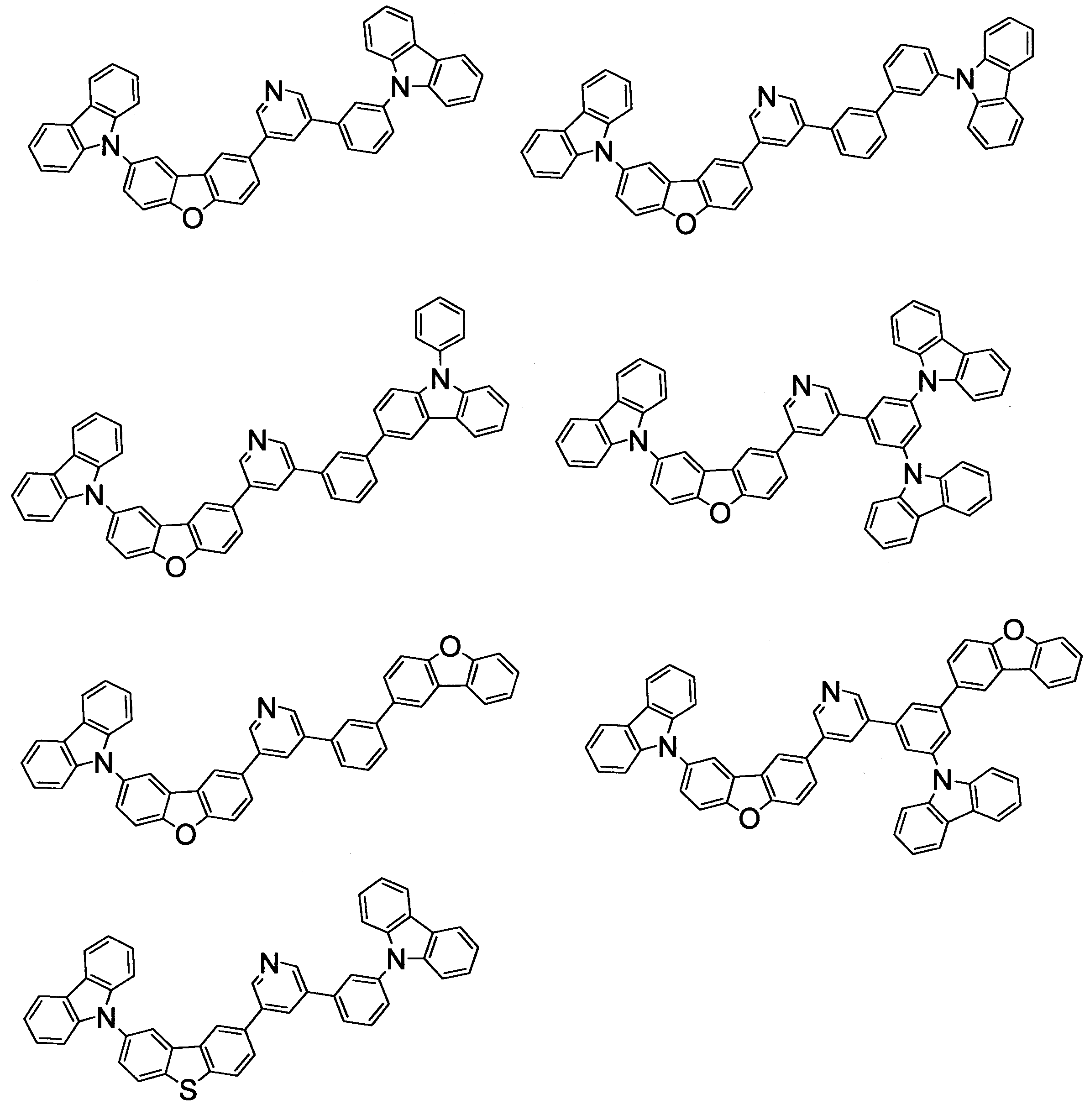


Specific examples of the compound represented by the above formula (A) are shown below.
本発明の含窒素へテロ芳香族環化合物は、有機EL素子を構成する有機薄膜層の材料として好適に使用できる。
本発明の有機EL素子用材料は、燐光型有機EL素子の材料、特に青色燐光発光素子の材料として好ましく用いることができ、燐光発光する有機EL素子の発光層や、発光層に隣接する層、例えば、正孔障壁層や電子障壁層の材料等として特に好ましい。 The nitrogen-containing heteroaromatic ring compound of the present invention can be suitably used as a material for an organic thin film layer constituting an organic EL device.
The material for an organic EL element of the present invention can be preferably used as a material for a phosphorescent organic EL element, particularly a blue phosphorescent light emitting element, and a light emitting layer of a phosphorescent organic EL element, a layer adjacent to the light emitting layer, For example, it is particularly preferable as a material for a hole barrier layer or an electron barrier layer.
続いて、本発明の有機EL素子について説明する。
本発明の有機EL素子は、陽極と陰極の間に、発光層を含む一層以上の有機薄膜層を有する。そして、有機薄膜層の少なくとも一層が、本発明の有機EL素子用材料を含有する。 Next, the organic EL element of the present invention will be described.
The organic EL device of the present invention has one or more organic thin film layers including a light emitting layer between an anode and a cathode. And at least one layer of an organic thin film layer contains the organic EL element material of this invention.
図1は、本発明の有機EL素子の一実施形態の層構成を示す概略図である。
有機EL素子1は、基板10上に、陽極20、正孔輸送帯域30、燐光発光層40、電子輸送帯域50及び陰極60を、この順で積層した構成を有する。正孔輸送帯域30は、正孔輸送層又は正孔注入層等を意味する。同様に、電子輸送帯域50は、電子輸送層又は電子注入層等を意味する。これらは形成しなくともよいが、好ましくは1層以上形成する。この素子において有機薄膜層は、正孔輸送帯域30に設けられる各有機層、燐光発光層40及び電子輸送帯域50に設けられる各有機層である。これら有機薄膜層のうち、少なくとも1層が本発明の有機EL素子用材料を含有する。これにより、有機EL素子の駆動電圧を低くできる。
尚、本発明の有機EL素子用材料を含有する有機薄膜層に対するこの材料の含有量は、好ましくは1~100重量%である。 FIG. 1 is a schematic view showing a layer structure of an embodiment of the organic EL device of the present invention.
Theorganic EL element 1 has a configuration in which an anode 20, a hole transport zone 30, a phosphorescent light emitting layer 40, an electron transport zone 50, and a cathode 60 are laminated on a substrate 10 in this order. The hole transport zone 30 means a hole transport layer or a hole injection layer. Similarly, the electron transport zone 50 means an electron transport layer, an electron injection layer, or the like. These need not be formed, but preferably one or more layers are formed. In this element, the organic thin film layer is each organic layer provided in the hole transport zone 30, each phosphor layer and the organic layer provided in the electron transport zone 50. Among these organic thin film layers, at least one layer contains the organic EL element material of the present invention. Thereby, the drive voltage of an organic EL element can be lowered.
The content of this material with respect to the organic thin film layer containing the organic EL device material of the present invention is preferably 1 to 100% by weight.
有機EL素子1は、基板10上に、陽極20、正孔輸送帯域30、燐光発光層40、電子輸送帯域50及び陰極60を、この順で積層した構成を有する。正孔輸送帯域30は、正孔輸送層又は正孔注入層等を意味する。同様に、電子輸送帯域50は、電子輸送層又は電子注入層等を意味する。これらは形成しなくともよいが、好ましくは1層以上形成する。この素子において有機薄膜層は、正孔輸送帯域30に設けられる各有機層、燐光発光層40及び電子輸送帯域50に設けられる各有機層である。これら有機薄膜層のうち、少なくとも1層が本発明の有機EL素子用材料を含有する。これにより、有機EL素子の駆動電圧を低くできる。
尚、本発明の有機EL素子用材料を含有する有機薄膜層に対するこの材料の含有量は、好ましくは1~100重量%である。 FIG. 1 is a schematic view showing a layer structure of an embodiment of the organic EL device of the present invention.
The
The content of this material with respect to the organic thin film layer containing the organic EL device material of the present invention is preferably 1 to 100% by weight.
本発明の有機EL素子においては、燐光発光層40が本発明の有機EL素子用材料を含有することが好ましく、特に、発光層のホスト材料として使用することが好ましい。本発明の材料は、3重項エネルギーが十分に大きいため、青色の燐光発光性ドーパント材料を使用しても、燐光発光性ドーパント材料の三重項エネルギーを効率的に発光層内に閉じ込めることができる。尚、青色発光層に限らず、より長波長の光(緑~赤色等)の発光層にも使用できる。
In the organic EL device of the present invention, the phosphorescent light emitting layer 40 preferably contains the material for the organic EL device of the present invention, and particularly preferably used as a host material for the light emitting layer. Since the triplet energy of the material of the present invention is sufficiently large, even when a blue phosphorescent dopant material is used, the triplet energy of the phosphorescent dopant material can be efficiently confined in the light emitting layer. . In addition, it can be used not only for the blue light emitting layer but also for a light emitting layer of longer wavelength light (such as green to red).
燐光発光層は、燐光発光性材料(燐光ドーパント)を含有する。燐光ドーパントとしては、金属錯体化合物が挙げられ、好ましくはIr,Pt,Os,Au,Cu,Re及びRuから選択される金属原子と、配位子とを有する化合物である。配位子は、オルトメタル結合を有すると好ましい。
燐光量子収率が高く、発光素子の外部量子効率をより向上させることができるという点で、燐光ドーパントは、Ir,Os及びPtから選ばれる金属原子を含有する化合物であると好ましく、イリジウム錯体、オスミウム錯体、白金錯体等の金属錯体であるとさらに好ましく、中でもイリジウム錯体及び白金錯体がより好ましく、オルトメタル化イリジウム錯体が最も好ましい。ドーパントは、1種単独でも、2種以上の混合物でもよい。 The phosphorescent light emitting layer contains a phosphorescent material (phosphorescent dopant). Examples of the phosphorescent dopant include metal complex compounds, preferably a compound having a metal atom selected from Ir, Pt, Os, Au, Cu, Re and Ru and a ligand. The ligand preferably has an ortho metal bond.
The phosphorescent dopant is preferably a compound containing a metal atom selected from Ir, Os and Pt in that the phosphorescent quantum yield is high and the external quantum efficiency of the light-emitting element can be further improved, and an iridium complex, It is more preferable that it is a metal complex such as an osmium complex and a platinum complex, among which an iridium complex and a platinum complex are more preferable, and an orthometalated iridium complex is most preferable. The dopant may be a single type or a mixture of two or more types.
燐光発光層における燐光ドーパントの添加濃度は特に限定されるものではないが、好ましくは0.1~30重量%(wt%)、より好ましくは0.1~20重量%(wt%)である
The addition concentration of the phosphorescent dopant in the phosphorescent light emitting layer is not particularly limited, but is preferably 0.1 to 30% by weight (wt%), more preferably 0.1 to 20% by weight (wt%).
また、燐光発光層40に隣接する層に本発明の材料を使用することも好ましい。例えば、図1の素子の正孔輸送帯域30と燐光発光層40の間に、本発明の材料を含有する層(陽極側隣接層)を形成した場合、該層は電子障壁層としての機能や励起子阻止層としての機能を有する。
一方、燐光発光層40と電子輸送帯域50の間に本発明の材料を含有する層(陰極側隣接層)を形成した場合、該層は正孔障壁層としての機能や励起子阻止層としての機能を有する。
尚、障壁層(阻止層)とは、キャリアの移動障壁、又は励起子の拡散障壁の機能を有する層である。発光層から正孔輸送帯域へ電子が漏れることを防ぐための有機層を主に電子障壁層と定義し、発光層から電子輸送帯域へ正孔が漏れることを防ぐための有機層を正孔障壁層と定義することがある。また、発光層で生成された三重項励起子が、三重項エネルギーが発光層よりも低い準位を有する周辺層へ拡散することを防止するための有機層を励起子阻止層(トリプレット障壁層)と定義することがある。
また本発明の材料を燐光発光層40に隣接する層に用い,かつ更にその隣接する層に接合する他の有機薄膜層に用いることもできる。 It is also preferable to use the material of the present invention in a layer adjacent to the phosphorescentlight emitting layer 40. For example, when a layer containing the material of the present invention (an anode side adjacent layer) is formed between the hole transport zone 30 and the phosphorescent light emitting layer 40 of the device of FIG. 1, the layer functions as an electron barrier layer. It functions as an exciton blocking layer.
On the other hand, when a layer (cathode side adjacent layer) containing the material of the present invention is formed between the phosphorescentlight emitting layer 40 and the electron transport zone 50, the layer functions as a hole blocking layer or as an exciton blocking layer. It has a function.
The barrier layer (blocking layer) is a layer having a function of a carrier movement barrier or an exciton diffusion barrier. The organic layer for preventing electrons from leaking from the light-emitting layer to the hole transport zone is mainly defined as an electron barrier layer, and the organic layer for preventing holes from leaking from the light-emitting layer to the electron transport zone is defined as a hole barrier. Sometimes defined as a layer. In addition, an exciton blocking layer (triplet barrier layer) is an organic layer for preventing triplet excitons generated in the light emitting layer from diffusing into a peripheral layer having triplet energy lower than that of the light emitting layer. It may be defined as
Further, the material of the present invention can be used for a layer adjacent to the phosphorescentlight emitting layer 40 and further used for another organic thin film layer bonded to the adjacent layer.
一方、燐光発光層40と電子輸送帯域50の間に本発明の材料を含有する層(陰極側隣接層)を形成した場合、該層は正孔障壁層としての機能や励起子阻止層としての機能を有する。
尚、障壁層(阻止層)とは、キャリアの移動障壁、又は励起子の拡散障壁の機能を有する層である。発光層から正孔輸送帯域へ電子が漏れることを防ぐための有機層を主に電子障壁層と定義し、発光層から電子輸送帯域へ正孔が漏れることを防ぐための有機層を正孔障壁層と定義することがある。また、発光層で生成された三重項励起子が、三重項エネルギーが発光層よりも低い準位を有する周辺層へ拡散することを防止するための有機層を励起子阻止層(トリプレット障壁層)と定義することがある。
また本発明の材料を燐光発光層40に隣接する層に用い,かつ更にその隣接する層に接合する他の有機薄膜層に用いることもできる。 It is also preferable to use the material of the present invention in a layer adjacent to the phosphorescent
On the other hand, when a layer (cathode side adjacent layer) containing the material of the present invention is formed between the phosphorescent
The barrier layer (blocking layer) is a layer having a function of a carrier movement barrier or an exciton diffusion barrier. The organic layer for preventing electrons from leaking from the light-emitting layer to the hole transport zone is mainly defined as an electron barrier layer, and the organic layer for preventing holes from leaking from the light-emitting layer to the electron transport zone is defined as a hole barrier. Sometimes defined as a layer. In addition, an exciton blocking layer (triplet barrier layer) is an organic layer for preventing triplet excitons generated in the light emitting layer from diffusing into a peripheral layer having triplet energy lower than that of the light emitting layer. It may be defined as
Further, the material of the present invention can be used for a layer adjacent to the phosphorescent
さらに、発光層を2層以上形成する場合、発光層間に形成するスペース層としても好適である。
図2は、本発明の有機EL素子の他の実施形態の層構成を示す概略図である。
有機EL素子2は、燐光発光層と蛍光発光層を積層したハイブリッド型の有機EL素子の例である。
有機EL素子2は、燐光発光層40と電子輸送帯域50の間にスペース層42と蛍光発光層44を形成した他は、上記有機EL素子1と同様な構成を有する。燐光発光層40及び蛍光発光層44を積層した構成では、燐光発光層40で形成された励起子を蛍光発光層44に拡散させないため、蛍光発光層44と燐光発光層40の間にスペース層42を設けることがある。本発明の材料は、三重項エネルギーが大きいため、スペース層として機能できる。 Furthermore, when two or more light emitting layers are formed, it is also suitable as a space layer formed between the light emitting layers.
FIG. 2 is a schematic view showing the layer structure of another embodiment of the organic EL device of the present invention.
The organic EL element 2 is an example of a hybrid type organic EL element in which a phosphorescent light emitting layer and a fluorescent light emitting layer are laminated.
The organic EL element 2 has the same configuration as theorganic EL element 1 except that a space layer 42 and a fluorescent light emitting layer 44 are formed between the phosphorescent light emitting layer 40 and the electron transport zone 50. In the configuration in which the phosphorescent light emitting layer 40 and the fluorescent light emitting layer 44 are laminated, the excitons formed in the phosphorescent light emitting layer 40 are not diffused into the fluorescent light emitting layer 44, so that a space layer 42 is provided between the fluorescent light emitting layer 44 and the phosphorescent light emitting layer 40. May be provided. Since the material of the present invention has a large triplet energy, it can function as a space layer.
図2は、本発明の有機EL素子の他の実施形態の層構成を示す概略図である。
有機EL素子2は、燐光発光層と蛍光発光層を積層したハイブリッド型の有機EL素子の例である。
有機EL素子2は、燐光発光層40と電子輸送帯域50の間にスペース層42と蛍光発光層44を形成した他は、上記有機EL素子1と同様な構成を有する。燐光発光層40及び蛍光発光層44を積層した構成では、燐光発光層40で形成された励起子を蛍光発光層44に拡散させないため、蛍光発光層44と燐光発光層40の間にスペース層42を設けることがある。本発明の材料は、三重項エネルギーが大きいため、スペース層として機能できる。 Furthermore, when two or more light emitting layers are formed, it is also suitable as a space layer formed between the light emitting layers.
FIG. 2 is a schematic view showing the layer structure of another embodiment of the organic EL device of the present invention.
The organic EL element 2 is an example of a hybrid type organic EL element in which a phosphorescent light emitting layer and a fluorescent light emitting layer are laminated.
The organic EL element 2 has the same configuration as the
有機EL素子2において、例えば、燐光発光層を黄色発光とし、蛍光発光層を青色発光層とすることにより、白色発光の有機EL素子が得られる。尚、本実施形態では燐光発光層及び蛍光発光層を1層ずつとしているが、これに限らず、それぞれ2層以上形成してもよく、照明や表示装置等、用途に合わせて適宜設定できる。例えば、白色発光素子とカラーフィルタを利用してフルカラー発光装置とする場合、演色性の観点から、赤、緑、青(RGB)、赤、緑、青、黄(RGBY)等、複数の波長領域の発光を含んでいることが好ましい場合がある。
In the organic EL element 2, for example, a white light emitting organic EL element can be obtained by setting the phosphorescent light emitting layer to emit yellow light and the fluorescent light emitting layer to blue light emitting layer. In this embodiment, the phosphorescent light-emitting layer and the fluorescent light-emitting layer are formed one by one. However, the present invention is not limited to this, and two or more layers may be formed, and can be appropriately set according to the application such as lighting and display device. For example, when a full color light emitting device is formed using a white light emitting element and a color filter, a plurality of wavelength regions such as red, green, blue (RGB), red, green, blue, yellow (RGBY) are used from the viewpoint of color rendering. In some cases, it may be preferable to include luminescence.
上述した実施形態の他に、本発明の有機EL素子は、公知の様々な構成を採用できる。また、発光層の発光は、陽極側、陰極側、あるいは両側から取り出すことができる。
In addition to the above-described embodiments, the organic EL element of the present invention can employ various known configurations. Further, light emission of the light emitting layer can be taken out from the anode side, the cathode side, or both sides.
(電子供与性ドーパント及び有機金属錯体)
本発明の有機EL素子は、陰極と有機薄膜層との界面領域に電子供与性ドーパント及び有機金属錯体の少なくともいずれかを有することも好ましい。
このような構成によれば、有機EL素子における発光輝度の向上や長寿命化が図られる。
電子供与性ドーパントとしては、アルカリ金属、アルカリ金属化合物、アルカリ土類金属、アルカリ土類金属化合物、希土類金属、及び希土類金属化合物等から選ばれた少なくとも一種類が挙げられる。
有機金属錯体としては、アルカリ金属を含む有機金属錯体、アルカリ土類金属を含む有機金属錯体、及び希土類金属を含む有機金属錯体等から選ばれた少なくとも一種類が挙げられる。 (Electron donating dopant and organometallic complex)
The organic EL device of the present invention preferably has at least one of an electron donating dopant and an organometallic complex in an interface region between the cathode and the organic thin film layer.
According to such a configuration, it is possible to improve the light emission luminance and extend the life of the organic EL element.
Examples of the electron donating dopant include at least one selected from alkali metals, alkali metal compounds, alkaline earth metals, alkaline earth metal compounds, rare earth metals, rare earth metal compounds, and the like.
Examples of the organometallic complex include at least one selected from an organometallic complex containing an alkali metal, an organometallic complex containing an alkaline earth metal, an organometallic complex containing a rare earth metal, and the like.
アルカリ金属としては、リチウム(Li)(仕事関数:2.93eV)、ナトリウム(Na)(仕事関数:2.36eV)、カリウム(K)(仕事関数:2.28eV)、ルビジウム(Rb)(仕事関数:2.16eV)、セシウム(Cs)(仕事関数:1.95eV)等が挙げられ、仕事関数が2.9eV以下のものが特に好ましい。これらのうち好ましくはK、Rb、Cs、さらに好ましくはRb又はCsであり、最も好ましくはCsである。
アルカリ土類金属としては、カルシウム(Ca)(仕事関数:2.9eV)、ストロンチウム(Sr)(仕事関数:2.0eV以上2.5eV以下)、バリウム(Ba)(仕事関数:2.52eV)等が挙げられ、仕事関数が2.9eV以下のものが特に好ましい。
希土類金属としては、スカンジウム(Sc)、イットリウム(Y)、セリウム(Ce)、テルビウム(Tb)、イッテルビウム(Yb)等が挙げられ、仕事関数が2.9eV以下のものが特に好ましい。
以上の金属のうち好ましい金属は、特に還元能力が高く、電子注入域への比較的少量の添加により、有機EL素子における発光輝度の向上や長寿命化が可能である。 Examples of the alkali metal include lithium (Li) (work function: 2.93 eV), sodium (Na) (work function: 2.36 eV), potassium (K) (work function: 2.28 eV), rubidium (Rb) (work Function: 2.16 eV), cesium (Cs) (work function: 1.95 eV) and the like, and those having a work function of 2.9 eV or less are particularly preferable. Of these, K, Rb, and Cs are preferred, Rb and Cs are more preferred, and Cs is most preferred.
Examples of the alkaline earth metal include calcium (Ca) (work function: 2.9 eV), strontium (Sr) (work function: 2.0 eV to 2.5 eV), barium (Ba) (work function: 2.52 eV). A work function of 2.9 eV or less is particularly preferable.
Examples of the rare earth metal include scandium (Sc), yttrium (Y), cerium (Ce), terbium (Tb), ytterbium (Yb) and the like, and those having a work function of 2.9 eV or less are particularly preferable.
Among the above metals, preferred metals are particularly high in reducing ability, and by adding a relatively small amount to the electron injection region, it is possible to improve the light emission luminance and extend the life of the organic EL element.
アルカリ金属化合物としては、酸化リチウム(Li2O)、酸化セシウム(Cs2O)、酸化カリウム(K2O)等のアルカリ酸化物、フッ化リチウム(LiF)、フッ化ナトリウム(NaF)、フッ化セシウム(CsF)、フッ化カリウム(KF)等のアルカリハロゲン化物等が挙げられ、フッ化リチウム(LiF)、酸化リチウム(Li2O)、フッ化ナトリウム(NaF)が好ましい。
アルカリ土類金属化合物としては、酸化バリウム(BaO)、酸化ストロンチウム(SrO)、酸化カルシウム(CaO)及びこれらを混合したストロンチウム酸バリウム(BaxSr1-xO)(0<x<1)、カルシウム酸バリウム(BaxCa1-xO)(0<x<1)等が挙げられ、BaO、SrO、CaOが好ましい。
希土類金属化合物としては、フッ化イッテルビウム(YbF3)、フッ化スカンジウム(ScF3)、酸化スカンジウム(ScO3)、酸化イットリウム(Y2O3)、酸化セリウム(Ce2O3)、フッ化ガドリニウム(GdF3)、フッ化テルビウム(TbF3)等が挙げられ、YbF3、ScF3、TbF3が好ましい。 Examples of the alkali metal compound include lithium oxide (Li 2 O), cesium oxide (Cs 2 O), alkali oxides such as potassium oxide (K 2 O), lithium fluoride (LiF), sodium fluoride (NaF), fluorine. Examples thereof include alkali halides such as cesium fluoride (CsF) and potassium fluoride (KF), and lithium fluoride (LiF), lithium oxide (Li 2 O), and sodium fluoride (NaF) are preferable.
Examples of the alkaline earth metal compound include barium oxide (BaO), strontium oxide (SrO), calcium oxide (CaO), and barium strontium oxide (Ba x Sr 1-x O) (0 <x <1), Examples thereof include barium calcium oxide (Ba x Ca 1-x O) (0 <x <1), and BaO, SrO, and CaO are preferable.
The rare earth metal compound, ytterbium fluoride (YbF 3), scandium fluoride (ScF 3), scandium oxide (ScO 3), yttrium oxide (Y 2 O 3), cerium oxide (Ce 2 O 3), gadolinium fluoride (GdF 3), include such terbium fluoride (TbF 3) is, YbF 3, ScF 3, TbF 3 are preferable.
有機金属錯体としては、上記の通り、それぞれ金属イオンとしてアルカリ金属イオン、アルカリ土類金属イオン、希土類金属イオンの少なくとも一つ含有するものであれば特に限定はない。また、配位子にはキノリノール、ベンゾキノリノール、アクリジノール、フェナントリジノール、ヒドロキシフェニルオキサゾール、ヒドロキシフェニルチアゾール、ヒドロキシジアリールオキサジアゾール、ヒドロキシジアリールチアジアゾール、ヒドロキシフェニルピリジン、ヒドロキシフェニルベンゾイミダゾール、ヒドロキシベンゾトリアゾール、ヒドロキシフルボラン、ビピリジル、フェナントロリン、フタロシアニン、ポルフィリン、シクロペンタジエン、β-ジケトン類、アゾメチン類、及びそれらの誘導体等が好ましいが、これらに限定されるものではない。
The organometallic complex is not particularly limited as long as it contains at least one of an alkali metal ion, an alkaline earth metal ion, and a rare earth metal ion as a metal ion as described above. The ligands include quinolinol, benzoquinolinol, acridinol, phenanthridinol, hydroxyphenyloxazole, hydroxyphenylthiazole, hydroxydiaryloxadiazole, hydroxydiarylthiadiazole, hydroxyphenylpyridine, hydroxyphenylbenzimidazole, hydroxybenzotriazole, Hydroxyfulborane, bipyridyl, phenanthroline, phthalocyanine, porphyrin, cyclopentadiene, β-diketones, azomethines, and derivatives thereof are preferred, but are not limited thereto.
電子供与性ドーパント及び有機金属錯体の添加形態としては、界面領域に層状又は島状に形成することが好ましい。形成方法としては、抵抗加熱蒸着法により電子供与性ドーパント及び有機金属錯体の少なくともいずれかを蒸着しながら、界面領域を形成する発光材料や電子注入材料である有機物を同時に蒸着させ、有機物中に電子供与性ドーパント及び有機金属錯体還元ドーパントの少なくともいずれかを分散する方法が好ましい。分散濃度は通常、モル比で有機物:電子供与性ドーパント及び/又は有機金属錯体=100:1~1:100であり、好ましくは5:1~1:5である。
As the addition form of the electron donating dopant and the organometallic complex, it is preferable to form a layer or an island in the interface region. As a forming method, while depositing at least one of an electron donating dopant and an organometallic complex by a resistance heating vapor deposition method, an organic material as a light emitting material or an electron injection material for forming an interface region is simultaneously deposited, and an electron is deposited in the organic material. A method of dispersing at least one of a donor dopant and an organometallic complex reducing dopant is preferable. The dispersion concentration is usually organic substance: electron donating dopant and / or organometallic complex in a molar ratio of 100: 1 to 1: 100, preferably 5: 1 to 1: 5.
電子供与性ドーパント及び有機金属錯体の少なくともいずれかを層状に形成する場合は、界面の有機層である発光材料や電子注入材料を層状に形成した後に、電子供与性ドーパント及び有機金属錯体の少なくともいずれかを単独で抵抗加熱蒸着法により蒸着し、好ましくは層の厚み0.1nm以上15nm以下で形成する。
In the case where at least one of the electron donating dopant and the organometallic complex is formed in a layered form, after forming the light emitting material or the electron injecting material that is the organic layer at the interface in a layered form, at least one of the electron donating dopant and the organometallic complex is formed. These are vapor-deposited by a resistance heating vapor deposition method alone, preferably with a layer thickness of 0.1 nm to 15 nm.
電子供与性ドーパント及び有機金属錯体の少なくともいずれかを島状に形成する場合は、界面の有機層である発光材料や電子注入材料を島状に形成した後に、電子供与性ドーパント及び有機金属錯体の少なくともいずれかを単独で抵抗加熱蒸着法により蒸着し、好ましくは島の厚み0.05nm以上1nm以下で形成する。
In the case where at least one of an electron donating dopant and an organometallic complex is formed in an island shape, a light emitting material or an electron injecting material which is an organic layer at the interface is formed in an island shape, and then the electron donating dopant and the organometallic complex are formed. At least one of them is vapor-deposited by a resistance heating vapor deposition method, preferably with an island thickness of 0.05 nm to 1 nm.
また、本発明の有機EL素子における、主成分と、電子供与性ドーパント及び有機金属錯体の少なくともいずれかの割合としては、モル比で、主成分:電子供与性ドーパント及び/又は有機金属錯体=5:1~1:5であると好ましく、2:1~1:2であるとさらに好ましい。
In the organic EL device of the present invention, the ratio of at least one of the main component and the electron donating dopant and the organometallic complex is, as a molar ratio, the main component: the electron donating dopant and / or the organometallic complex = 5. It is preferably 1 to 1: 5, and more preferably 2: 1 to 1: 2.
本発明の有機EL素子では、上述した本発明の有機EL素子用材料を使用した層以外の構成については、特に限定されず、公知の材料等を使用できる。以下、実施形態1の素子の層について簡単に説明するが、本発明の有機EL素子に適用される材料は以下に限定されない。
In the organic EL element of the present invention, the configuration other than the layer using the organic EL element material of the present invention described above is not particularly limited, and a known material or the like can be used. Hereinafter, although the layer of the element of Embodiment 1 is demonstrated easily, the material applied to the organic EL element of this invention is not limited to the following.
[基板]
基板としてはガラス板、ポリマー板等を用いることができる。
ガラス板としては、特にソーダ石灰ガラス、バリウム・ストロンチウム含有ガラス、鉛ガラス、アルミノケイ酸ガラス、ホウケイ酸ガラス、バリウムホウケイ酸ガラス、石英等が挙げられる。また、ポリマー板としては、ポリカーボネート、アクリル、ポリエチレンテレフタレート、ポリエーテルサルフォン、ポリサルフォン等を挙げることができる。 [substrate]
As the substrate, a glass plate, a polymer plate or the like can be used.
Examples of the glass plate include soda lime glass, barium / strontium-containing glass, lead glass, aluminosilicate glass, borosilicate glass, barium borosilicate glass, and quartz. Examples of the polymer plate include polycarbonate, acrylic, polyethylene terephthalate, polyether sulfone, and polysulfone.
[陽極]
陽極は例えば導電性材料からなり、4eVより大きな仕事関数を有する導電性材料が適している。
上記導電性材料としては、炭素、アルミニウム、バナジウム、鉄、コバルト、ニッケル、タングステン、銀、金、白金、パラジウム等及びそれらの合金、ITO基板、NESA基板に使用される酸化スズ、酸化インジウム等の酸化金属、さらにはポリチオフェンやポリピロール等の有機導電性樹脂が挙げられる。
陽極は、必要があれば2層以上の層構成により形成されていてもよい。 [anode]
The anode is made of, for example, a conductive material, and a conductive material having a work function larger than 4 eV is suitable.
Examples of the conductive material include carbon, aluminum, vanadium, iron, cobalt, nickel, tungsten, silver, gold, platinum, palladium, and their alloys, ITO substrate, tin oxide used for NESA substrate, indium oxide, and the like. Examples thereof include metal oxides and organic conductive resins such as polythiophene and polypyrrole.
The anode may be formed with a layer structure of two or more layers if necessary.
[陰極]
陰極は例えば導電性材料からなり、4eVより小さな仕事関数を有する導電性材料が適している。
上記導電性材料としては、マグネシウム、カルシウム、錫、鉛、チタニウム、イットリウム、リチウム、ルテニウム、マンガン、アルミニウム、フッ化リチウム等及びこれらの合金が挙げられるが、これらに限定されるものではない。
また、上記合金としては、マグネシウム/銀、マグネシウム/インジウム、リチウム/アルミニウム等が代表例として挙げられるが、これらに限定されるものではない。合金の比率は、蒸着源の温度、雰囲気、真空度等により制御され、適切な比率に選択される。
陰極は、必要があれば2層以上の層構成により形成されていてもよく、陰極は上記導電性材料を蒸着やスパッタリング等の方法により薄膜を形成させることにより、作製することができる。 [cathode]
The cathode is made of, for example, a conductive material, and a conductive material having a work function smaller than 4 eV is suitable.
Examples of the conductive material include, but are not limited to, magnesium, calcium, tin, lead, titanium, yttrium, lithium, ruthenium, manganese, aluminum, lithium fluoride, and alloys thereof.
Examples of the alloy include magnesium / silver, magnesium / indium, lithium / aluminum, and the like, but are not limited thereto. The ratio of the alloy is controlled by the temperature of the vapor deposition source, the atmosphere, the degree of vacuum, etc., and is selected to an appropriate ratio.
If necessary, the cathode may be formed with a layer structure of two or more layers, and the cathode can be produced by forming a thin film from the conductive material by a method such as vapor deposition or sputtering.
発光層からの発光を陰極から取り出す場合、陰極の発光に対する透過率は10%より大きくすることが好ましい。
また、陰極としてのシート抵抗は数百Ω/□以下が好ましく、膜厚は通常10nm~1μmであり、好ましくは50~200nmである。 When light emitted from the light emitting layer is taken out from the cathode, the transmittance of the cathode for light emission is preferably greater than 10%.
The sheet resistance as the cathode is preferably several hundred Ω / □ or less, and the film thickness is usually 10 nm to 1 μm, preferably 50 to 200 nm.
[発光層]
本発明の有機EL素子層材料以外の材料で燐光発光層を形成する場合、燐光発光層の材料として公知の材料が使用できる。具体的には、特願2005-517938等を参照すればよい。
本発明の有機EL素子は、図2に示す素子のように蛍光発光層を有していてもよい。蛍光発光層としては、公知の材料が使用できる。 [Light emitting layer]
When the phosphorescent light emitting layer is formed of a material other than the organic EL element layer material of the present invention, a known material can be used as the material of the phosphorescent light emitting layer. Specifically, Japanese Patent Application No. 2005-517938 may be referred to.
The organic EL device of the present invention may have a fluorescent light emitting layer like the device shown in FIG. A known material can be used for the fluorescent light emitting layer.
発光層は、ダブルホスト(ホスト・コホストともいう)としてもよい。具体的に、発光層において電子輸送性のホストと正孔輸送性のホストを組み合わせることで、発光層内のキャリアバランスを調整してもよい。
また、ダブルドーパントとしてもよい。発光層において、量子収率の高いドーパント材料を2種類以上入れることによって、それぞれのドーパントが発光する。例えば、ホストと赤色ドーパント、緑色のドーパントを共蒸着することによって、黄色の発光層を実現することがある。
発光層は単層でもよく、また、積層構造でもよい。発光層を積層させると、発光層界面に電子と正孔を蓄積させることによって再結合領域を発光層界面に集中させることができる。これによって、量子効率を向上させる。 The light emitting layer may be a double host (also referred to as a host / cohost). Specifically, the carrier balance in the light emitting layer may be adjusted by combining an electron transporting host and a hole transporting host in the light emitting layer.
Moreover, it is good also as a double dopant. In the light emitting layer, each dopant emits light by adding two or more dopant materials having a high quantum yield. For example, a yellow light emitting layer may be realized by co-evaporating a host, a red dopant, and a green dopant.
The light emitting layer may be a single layer or a laminated structure. When the light emitting layer is stacked, the recombination region can be concentrated on the light emitting layer interface by accumulating electrons and holes at the light emitting layer interface. This improves the quantum efficiency.
[正孔注入層及び正孔輸送層]
正孔注入・輸送層は、発光層への正孔注入を助け、発光領域まで輸送する層であって、正孔移動度が大きく、イオン化エネルギーが通常5.6eV以下と小さい層である。
正孔注入・輸送層の材料としては、より低い電界強度で正孔を発光層に輸送する材料が好ましく、さらに正孔の移動度が、例えば104~106V/cmの電界印加時に、少なくとも10-4cm2/V・秒であれば好ましい。 [Hole injection layer and hole transport layer]
The hole injection / transport layer is a layer that assists hole injection into the light emitting layer and transports it to the light emitting region, and has a high hole mobility and a small ionization energy of usually 5.6 eV or less.
As the material for the hole injection / transport layer, a material that transports holes to the light emitting layer with lower electric field strength is preferable. Further, when an electric field is applied with a hole mobility of, for example, 10 4 to 10 6 V / cm, At least 10 −4 cm 2 / V · sec is preferable.
正孔注入・輸送層の材料としては、具体的には、トリアゾール誘導体(米国特許3,112,197号明細書等参照)、オキサジアゾール誘導体(米国特許3,189,447号明細書等参照)、イミダゾール誘導体(特公昭37-16096号公報等参照)、ポリアリールアルカン誘導体(米国特許3,615,402号明細書、同第3,820,989号明細書、同第3,542,544号明細書、特公昭45-555号公報、同51-10983号公報、特開昭51-93224号公報、同55-17105号公報、同56-4148号公報、同55-108667号公報、同55-156953号公報、同 56-36656号公報等参照)、ピラゾリン誘導体及びピラゾロン誘導体(米国特許第3,180,729号明細書、同第4,278,746号明細書、特開昭55-88064号公報、同55-88065号公報、同49-105537号公報、同55-51086号公報、同56-80051号公報、同56-88141号公報、同57-45545号公報、同54-112637号公報、同55-74546号公報等参照)、フェニレンジアミン誘導体(米国特許第3,615,404号明細書、特公昭51-10105号公報、同46-3712号公報、同47-25336号公報、同54-119925号公報等参照)、アリールアミン誘導体(米国特許第3,567,450号明細書、同第3,240,597号明細書、同第3,658,520号明細書、同第4,232,103号明細書、同第4,175,961号明細書、同第4,012,376号明細書、特公昭49-35702号公報、同39-27577号公報、特開昭55-144250号公報、同56-119132号公報、同56-22437号公報、西独特許第1,110,518号明細書等参照)、アミノ置換カルコン誘導体(米国特許第3,526,501号明細書等参照)、オキサゾール誘導体(米国特許第3,257,203号明細書等に開示のもの)、スチリルアントラセン誘導体(特開昭56-46234号公報等参照)、フルオレノン誘導体(特開昭54-110837号公報等参照)、ヒドラゾン誘導体(米国特許第3,717,462号明細書、特開昭54-59143号公報、同55-52063号公報、同55-52064号公報、同55-46760号公報、同57-11350号公報、同57-148749号公報、特開平2-311591号公報等参照)、スチルベン誘導体(特開昭61-210363号公報、同第61-228451号公報、同61-14642号公報、同61-72255号公報、同62-47646号公報、同62-36674号公報、同62-10652号公報、同62-30255号公報、同60-93455号公報、同60-94462号公報、同60-174749号公報、同60-175052号公報等参照)、シラザン誘導体(米国特許第4,950,950号明細書)、ポリシラン系(特開平2-204996号公報)、アニリン系共重合体(特開平2-282263号公報)等を挙げることができる。
また、p型Si、p型SiC等の無機化合物も正孔注入材料として使用することができる。 Specific examples of the material for the hole injection / transport layer include triazole derivatives (see US Pat. No. 3,112,197) and oxadiazole derivatives (see US Pat. No. 3,189,447). ), Imidazole derivatives (see JP-B-37-16096, etc.), polyarylalkane derivatives (US Pat. Nos. 3,615,402, 3,820,989, 3,542,544) Nos. 45-555, 51-10983, 51-93224, 55-17105, 56-4148, 55-108667, 55-156953, 56-36656, etc.), pyrazoline derivatives and pyrazolone derivatives (US Pat. No. 3,180,729, No. 4) 278,746, JP 55-88064, 55-88065, 49-105537, 55-51086, 56-80051, 56-88141. No. 57-45545, No. 54-112537, No. 55-74546, etc.), phenylenediamine derivatives (US Pat. No. 3,615,404, JP-B 51-10105, 46-3712, 47-25336, 54-1119925, etc.), arylamine derivatives (US Pat. Nos. 3,567,450, 3,240,597) No. 3,658,520, No. 4,232,103, No. 4,175,961, No. 4,012,376 Description, JP-B-49-35702, JP-A-39-27577, JP-A-55-144250, JP-A-56-119132, JP-A-56-22437, West German Patent No. 1,110,518 ), Amino-substituted chalcone derivatives (see US Pat. No. 3,526,501, etc.), oxazole derivatives (disclosed in US Pat. No. 3,257,203 etc.), styrylanthracene derivatives (See JP 56-46234 A, etc.), fluorenone derivatives (see JP 54-110837 A, etc.), hydrazone derivatives (US Pat. No. 3,717,462, JP 54-59143 A). Gazette, 55-52063, 55-52064, 55-46760, 57-11350, 57 No. 148749, JP-A-2-311591, etc.), stilbene derivatives (JP-A Nos. 61-210363, 61-228451, 61-14642, 61-72255, etc.) 62-47646, 62-36684, 62-10652, 62-30255, 60-93455, 60-94462, 60-174749, 60 -175052, etc.), silazane derivatives (US Pat. No. 4,950,950), polysilanes (JP-A-2-204996), aniline copolymers (JP-A-2-282263) Etc.
In addition, inorganic compounds such as p-type Si and p-type SiC can also be used as the hole injection material.
正孔注入・輸送層の材料には架橋型材料を用いることができ、架橋型の正孔注入輸送層としては、例えば、Chem.Mater.2008,20,413-422、Chem.Mater.2011,23(3),658-681、WO2008108430、WO2009102027、WO2009123269、WO2010016555、WO2010018813等の架橋材を、熱、光等により不溶化した層が挙げられる。
As the material of the hole injection / transport layer, a cross-linkable material can be used. As the cross-linkable hole injection / transport layer, for example, Chem. Mater. 2008, 20, 413-422, Chem. Mater. Examples include a layer obtained by insolubilizing a cross-linking material such as 2011, 23 (3), 658-681, WO2008108430, WO2009102027, WO2009123269, WO2010016555, WO2010018813 by heat, light or the like.
[電子注入層及び電子輸送層]
電子注入・輸送層は、発光層への電子の注入を助け、発光領域まで輸送する層であって、電子移動度が大きい層である。
有機EL素子は発光した光が電極(例えば陰極)により反射するため、直接陽極から取り出される発光と、電極による反射を経由して取り出される発光とが干渉することが知られている。この干渉効果を効率的に利用するため、電子注入・輸送層は数nm~数μmの膜厚で適宜選ばれるが、特に膜厚が厚いとき、電圧上昇を避けるために、104~106V/cmの電界印加時に電子移動度が少なくとも10-5cm2/Vs以上であることが好ましい。 [Electron injection layer and electron transport layer]
The electron injection / transport layer is a layer that assists the injection of electrons into the light emitting layer and transports it to the light emitting region, and has a high electron mobility.
In the organic EL element, since emitted light is reflected by an electrode (for example, a cathode), it is known that light emitted directly from the anode interferes with light emitted via reflection by the electrode. In order to efficiently use this interference effect, the electron injecting / transporting layer is appropriately selected with a film thickness of several nm to several μm. However, particularly when the film thickness is large, in order to avoid a voltage increase, 10 4 to 10 6. The electron mobility is preferably at least 10 −5 cm 2 / Vs or more when an electric field of V / cm is applied.
電子注入・輸送層に用いる電子輸送性材料としては、分子内にヘテロ原子を1個以上含有する芳香族ヘテロ環化合物が好ましく用いられ、特に含窒素環誘導体が好ましい。また、含窒素環誘導体としては、含窒素6員環もしくは5員環骨格を有する芳香族環、又は含窒素6員環もしくは5員環骨格を有する縮合芳香族環化合物が好ましく、例えば、ピリジン環、ピリミジン環、トリアジン環、ベンズイミダゾール環、フェナントロリン環、キナゾリン環等を骨格に含む化合物が挙げられる。
As the electron transporting material used for the electron injection / transport layer, an aromatic heterocyclic compound containing one or more heteroatoms in the molecule is preferably used, and a nitrogen-containing ring derivative is particularly preferable. The nitrogen-containing ring derivative is preferably an aromatic ring having a nitrogen-containing 6-membered ring or 5-membered ring skeleton, or a condensed aromatic ring compound having a nitrogen-containing 6-membered ring or 5-membered ring skeleton, such as a pyridine ring. , Pyrimidine ring, triazine ring, benzimidazole ring, phenanthroline ring, quinazoline ring and the like.
その他、ドナー性材料のドーピング(n)、アクセプター材料のドーピング(p)により、半導体性を備えた有機層を形成してもよい。Nドーピングの代表例は、電子輸送性材料にLiやCs等の金属をドーピングさせるものであり、Pドーピングの代表例は、正孔輸送性材料にF4TCNQ等のアクセプター材をドープするものである(例えば、特許3695714参照)。
In addition, an organic layer having semiconductivity may be formed by doping (n) with a donor material and doping (p) with an acceptor material. A typical example of N doping is to dope a metal such as Li or Cs into an electron transporting material, and a typical example of P doping is to dope an acceptor material such as F4TCNQ into a hole transporting material ( For example, see Japanese Patent No. 3695714).
本発明の有機EL素子の各層の形成は、真空蒸着、スパッタリング、プラズマ、イオンプレーティング等の乾式成膜法やスピンコーティング、ディッピング、フローコーティング等の湿式成膜法等の公知の方法を適用することができる。
各層の膜厚は特に限定されるものではないが、適切な膜厚に設定する必要がある。膜厚が厚すぎると、一定の光出力を得るために大きな印加電圧が必要になり効率が悪くなる。膜厚が薄すぎるとピンホール等が発生して、電界を印加しても充分な発光輝度が得られない。通常の膜厚は5nm~10μmの範囲が適しているが、10nm~0.2μmの範囲がさらに好ましい。 For the formation of each layer of the organic EL device of the present invention, a known method such as a dry film forming method such as vacuum deposition, sputtering, plasma, or ion plating, or a wet film forming method such as spin coating, dipping, or flow coating is applied. be able to.
The thickness of each layer is not particularly limited, but must be set to an appropriate thickness. If the film thickness is too thick, a large applied voltage is required to obtain a constant light output, resulting in poor efficiency. If the film thickness is too thin, pinholes and the like are generated, and sufficient light emission luminance cannot be obtained even when an electric field is applied. The normal film thickness is suitably in the range of 5 nm to 10 μm, but more preferably in the range of 10 nm to 0.2 μm.
[含窒素へテロ芳香族環化合物]
合成例1[化合物Aの合成]
(1)中間体Aの合成
以下の工程により中間体Aを合成した。

[Nitrogen-containing heteroaromatic ring compound]
Synthesis Example 1 [Synthesis of Compound A]
(1) Synthesis of Intermediate A Intermediate A was synthesized by the following steps.
合成例1[化合物Aの合成]
(1)中間体Aの合成
以下の工程により中間体Aを合成した。
Synthesis Example 1 [Synthesis of Compound A]
(1) Synthesis of Intermediate A Intermediate A was synthesized by the following steps.
アルゴン雰囲気下、カルバゾール16.7g(100mmol)、2,6-ジブロモピリジン23.7g(100mmol)、ヨウ化銅19.0g(100mmol)、trans-1,2-シクロヘキサンジアミン11.4g(100mmol)、リン酸三カリウム42.4g(200mmol)を脱水1,4-ジオキサン200mlに加えて、72時間加熱還流攪拌した。反応溶液を減圧下で濃縮して得られた残渣に、トルエン500mlを加えて120℃に加熱し、不溶物を濾別した。濾液を減圧下で濃縮して得られた残渣をシリカゲルカラムクロマトグラフィー(ヘキサン/トルエン=4/1)で精製することにより、中間体A9.7g(収率30%)を白色固体として得た。
Under an argon atmosphere, carbazole 16.7 g (100 mmol), 2,6-dibromopyridine 23.7 g (100 mmol), copper iodide 19.0 g (100 mmol), trans-1,2-cyclohexanediamine 11.4 g (100 mmol), 42.4 g (200 mmol) of tripotassium phosphate was added to 200 ml of dehydrated 1,4-dioxane, and the mixture was heated to reflux with stirring for 72 hours. To the residue obtained by concentrating the reaction solution under reduced pressure, 500 ml of toluene was added and heated to 120 ° C., and the insoluble material was filtered off. The residue obtained by concentrating the filtrate under reduced pressure was purified by silica gel column chromatography (hexane / toluene = 4/1) to obtain 9.7 g of Intermediate A (yield 30%) as a white solid.
(2)中間体Cの合成
以下の工程により中間体Cを合成した。

(2) Synthesis of Intermediate C Intermediate C was synthesized by the following steps.
以下の工程により中間体Cを合成した。
アルゴン雰囲気下、国際公開第2009-008100号パンフレットに記載の方法に従って合成した中間体B4.1g(10mmol)に脱水THF50mlを加え、-70℃で攪拌した。次いで、1.6Mのn-ブチルリチウムn-ヘキサン溶液6.25mlを滴下装入した。-70℃で1時間攪拌した後、ホウ酸トリイソプロピル5.6g(30mmol)を加え、-70℃で1時間攪拌した後、室温で5時間攪拌した。反応液を濃縮後、ジクロロメタン400mlと1N塩酸50mlを加えて、氷水浴下で、1時間攪拌した。有機相を分取して、無水硫酸マグネシウムで乾燥してから、濾液を濃縮した。得られた固体をヘキサン-トルエンの混合溶媒で懸濁洗浄することにより、中間体C2.3g(収率60%)を白色固体として得た。
In an argon atmosphere, 50 ml of dehydrated THF was added to 4.1 g (10 mmol) of Intermediate B synthesized according to the method described in International Publication No. 2009-008100 pamphlet, and the mixture was stirred at -70 ° C. Subsequently, 6.25 ml of 1.6M n-butyllithium n-hexane solution was added dropwise. After stirring at −70 ° C. for 1 hour, 5.6 g (30 mmol) of triisopropyl borate was added, stirred at −70 ° C. for 1 hour, and then stirred at room temperature for 5 hours. The reaction mixture was concentrated, 400 ml of dichloromethane and 50 ml of 1N hydrochloric acid were added, and the mixture was stirred for 1 hour in an ice-water bath. The organic phase was separated and dried over anhydrous magnesium sulfate, and the filtrate was concentrated. The obtained solid was suspended and washed with a mixed solvent of hexane-toluene to obtain 2.3 g of intermediate C (yield 60%) as a white solid.
(3)化合物Aの合成
以下の工程により化合物Aを合成した。

(3) Synthesis of Compound A Compound A was synthesized by the following steps.
以下の工程により化合物Aを合成した。
アルゴン雰囲気下、中間体A3.2g(10mmol)、中間体C3.8g(10mmol)、2M炭酸ナトリウム水溶液10ml、1,2-ジメトキシエタン(DME)10ml、トルエン30mlを加え、次いで、テトラキス(トリフェニルホスフィン)パラジウム0.34g(0.30mmol)を加えて、8時間加熱還流攪拌した。反応溶液を減圧下で濃縮して得られた残渣に、トルエン500mlを加えて120℃に加熱し、不溶物を濾別した。濾液を減圧下で濃縮して得られた残渣をシリカゲルカラムクロマトグラフィー(ヘキサン/ジクロロメタン=3/1)で精製することにより、化合物A4.3g(収率75%)を白色固体として得た。
FD-MS分析の結果、分子量575に対してm/e=575であった。 Under an argon atmosphere, 3.2 g (10 mmol) of intermediate A, 3.8 g (10 mmol) of intermediate C, 10 ml of 2M aqueous sodium carbonate solution, 10 ml of 1,2-dimethoxyethane (DME) and 30 ml of toluene were added, and then tetrakis (triphenyl) Phosphine) palladium (0.34 g, 0.30 mmol) was added, and the mixture was heated to reflux with stirring for 8 hours. To the residue obtained by concentrating the reaction solution under reduced pressure, 500 ml of toluene was added and heated to 120 ° C., and the insoluble material was filtered off. The filtrate was concentrated under reduced pressure, and the resulting residue was purified by silica gel column chromatography (hexane / dichloromethane = 3/1) to give 4.3 g (yield 75%) of compound A as a white solid.
As a result of FD-MS analysis, m / e = 575 with respect to the molecular weight of 575.
合成例2[化合物Bの合成]
(1)中間体Dの合成
以下の工程により中間体Dを合成した。

Synthesis Example 2 [Synthesis of Compound B]
(1) Synthesis of Intermediate D Intermediate D was synthesized by the following steps.
(1)中間体Dの合成
以下の工程により中間体Dを合成した。
(1) Synthesis of Intermediate D Intermediate D was synthesized by the following steps.
アルゴン雰囲気下、カルバゾール16.7g(100mmol)、3,5-ジブロモピリジン23.7g(100mmol)、ヨウ化銅19.0g(100mmol)、trans-1,2-シクロヘキサンジアミン11.4g(100mmol)、リン酸三カリウム42.4g(200mmol)を脱水1,4-ジオキサン200mlに加えて、96時間加熱還流攪拌した。反応溶液を減圧下で濃縮して得られた残渣に、トルエン500mlを加えて120℃に加熱し、不溶物を濾別した。濾液を減圧下で濃縮して得られた残渣をシリカゲルカラムクロマトグラフィー(ヘキサン/トルエン=4/1)で精製することにより、中間体D6.8g(収率21%)を白色固体として得た。
Under an argon atmosphere, carbazole 16.7 g (100 mmol), 3,5-dibromopyridine 23.7 g (100 mmol), copper iodide 19.0 g (100 mmol), trans-1,2-cyclohexanediamine 11.4 g (100 mmol), 42.4 g (200 mmol) of tripotassium phosphate was added to 200 ml of dehydrated 1,4-dioxane, and the mixture was heated to reflux with stirring for 96 hours. To the residue obtained by concentrating the reaction solution under reduced pressure, 500 ml of toluene was added and heated to 120 ° C., and the insoluble material was filtered off. The residue obtained by concentrating the filtrate under reduced pressure was purified by silica gel column chromatography (hexane / toluene = 4/1) to obtain 6.8 g of intermediate D (yield 21%) as a white solid.
(2)化合物Bの合成
以下の工程により化合物Bを合成した。

(2) Synthesis of Compound B Compound B was synthesized by the following steps.
以下の工程により化合物Bを合成した。
アルゴン雰囲気下、中間体D3.2g(10mmol)、実施例1(2)で得た中間体C3.8g(10mmol)、2M炭酸ナトリウム水溶液10ml、1,2-ジメトキシエタン(DME)10ml、トルエン30mlを加え、次いで、テトラキス(トリフェニルホスフィン)パラジウム0.34g(0.30mmol)を加えて、24時間加熱還流攪拌した。反応溶液を減圧下で濃縮して得られた残渣に、トルエン500mlを加えて120℃に加熱し、不溶物を濾別した。濾液を減圧下で濃縮して得られた残渣をシリカゲルカラムクロマトグラフィー(ヘキサン/ジクロロメタン=2/1)で精製することにより、化合物B3.2g(収率55%)を白色固体として得た。
FD-MS分析の結果、分子量575に対してm/e=575であった。
また、1H-NMRの測定結果を以下に示す。
・1H-NMR(400MHz、CDCl3)δ7.28-7.35(4H、m)、7.37-7.46(8H、m)、7.68(1H、dd、J=2.0Hz、8.4Hz)、7.78-7.84(3H、m)8.15-8.18(6H、m)、8.21-8.22(1H、m)、8.89(1H、d、J=2.0Hz)、9.03(1H、d、J=2.0Hz) Under an argon atmosphere, 3.2 g (10 mmol) of Intermediate D, 3.8 g (10 mmol) of Intermediate C obtained in Example 1 (2), 10 ml of 2M aqueous sodium carbonate solution, 10 ml of 1,2-dimethoxyethane (DME), 30 ml of toluene Then, 0.34 g (0.30 mmol) of tetrakis (triphenylphosphine) palladium was added, and the mixture was stirred with heating under reflux for 24 hours. To the residue obtained by concentrating the reaction solution under reduced pressure, 500 ml of toluene was added and heated to 120 ° C., and the insoluble material was filtered off. The filtrate was concentrated under reduced pressure, and the resulting residue was purified by silica gel column chromatography (hexane / dichloromethane = 2/1) to obtain 3.2 g (yield 55%) of compound B as a white solid.
As a result of FD-MS analysis, m / e = 575 with respect to the molecular weight of 575.
The measurement result of 1 H-NMR is shown below.
1 H-NMR (400 MHz, CDCl 3 ) δ 7.28-7.35 (4H, m), 7.37-7.46 (8H, m), 7.68 (1H, dd, J = 2.0 Hz) 8.4 Hz), 7.78-7.84 (3H, m) 8.15-8.18 (6H, m), 8.21-8.22 (1H, m), 8.89 (1H, d, J = 2.0 Hz), 9.03 (1H, d, J = 2.0 Hz)
合成例3[化合物Cの合成]
(1)中間体Eの合成
以下の工程により中間体Eを合成した。

Synthesis Example 3 [Synthesis of Compound C]
(1) Synthesis of Intermediate E Intermediate E was synthesized by the following steps.
(1)中間体Eの合成
以下の工程により中間体Eを合成した。
(1) Synthesis of Intermediate E Intermediate E was synthesized by the following steps.
アルゴン雰囲気下、ジベンゾフラン-2-ボロン酸21.2g(100mmol)、3,5-ジブロモピリジン23.7g(100mmol)、2M炭酸ナトリウム水溶液100ml、1,2-ジメトキシエタン(DME)100ml、トルエン200mlを加え、次いで、テトラキス(トリフェニルホスフィン)パラジウム3.5g(3mmol)を加えて、48時間加熱還流攪拌した。反応溶液を減圧下で濃縮して得られた残渣に、トルエン1000mlを加えて120℃に加熱し、不溶物を濾別した。濾液を減圧下で濃縮して得られた残渣をシリカゲルカラムクロマトグラフィー(ヘキサン/ジクロロメタン=2/1)で精製することにより、中間体E13.9g(収率43%)を白色固体として得た。
Under an argon atmosphere, 21.2 g (100 mmol) of dibenzofuran-2-boronic acid, 23.7 g (100 mmol) of 3,5-dibromopyridine, 100 ml of 2M sodium carbonate aqueous solution, 100 ml of 1,2-dimethoxyethane (DME), and 200 ml of toluene. Then, 3.5 g (3 mmol) of tetrakis (triphenylphosphine) palladium was added, and the mixture was heated to reflux with stirring for 48 hours. To the residue obtained by concentrating the reaction solution under reduced pressure, 1000 ml of toluene was added and heated to 120 ° C., and insoluble matters were filtered off. The residue obtained by concentrating the filtrate under reduced pressure was purified by silica gel column chromatography (hexane / dichloromethane = 2/1) to obtain 13.9 g of intermediate E (43% yield) as a white solid.
(2)化合物Cの合成
以下の工程により化合物Cを合成した。

(2) Synthesis of Compound C Compound C was synthesized by the following steps.
以下の工程により化合物Cを合成した。
アルゴン雰囲気下、中間体E3.2g(10mmol)、中間体C3.8g(10mmol)、2M炭酸ナトリウム水溶液10ml、1,2-ジメトキシエタン(DME)10ml、トルエン30mlを加え、次いで、テトラキス(トリフェニルホスフィン)パラジウム0.34g(0.30mmol)を加えて、48時間加熱還流攪拌した。反応溶液を減圧下で濃縮して得られた残渣に、トルエン500mlを加えて120℃に加熱し、不溶物を濾別した。濾液を減圧下で濃縮して得られた残渣をシリカゲルカラムクロマトグラフィー(ヘキサン/ジクロロメタン=3/2)で精製することにより、化合物C2.6g(収率45%)を白色固体として得た。
FD-MS分析の結果、分子量576に対してm/e=576であった。 Under an argon atmosphere, 3.2 g (10 mmol) of Intermediate E, 3.8 g (10 mmol) of Intermediate C, 10 ml of 2M aqueous sodium carbonate solution, 10 ml of 1,2-dimethoxyethane (DME) and 30 ml of toluene were added, followed by tetrakis (triphenyl) Phosphine) palladium (0.34 g, 0.30 mmol) was added, and the mixture was stirred with heating under reflux for 48 hours. To the residue obtained by concentrating the reaction solution under reduced pressure, 500 ml of toluene was added and heated to 120 ° C., and the insoluble material was filtered off. The residue obtained by concentrating the filtrate under reduced pressure was purified by silica gel column chromatography (hexane / dichloromethane = 3/2) to obtain 2.6 g (yield 45%) of compound C as a white solid.
As a result of FD-MS analysis, m / e = 576 with respect to the molecular weight of 576.
合成例4[化合物Dの合成]
(1)中間体Fの合成

アルゴン雰囲気下、3-(N-カルバゾリル)フェニルボロン酸28.7g(100mmol)、3,5-ジブロモピリジン23.7g(100mmol)、2M炭酸ナトリウム水溶液100ml、1,2-ジメトキシエタン(DME)100ml、トルエン200mlを加え、次いで、テトラキス(トリフェニルホスフィン)パラジウム3.5g(3mmol)を加えて、36時間加熱還流攪拌した。反応溶液を減圧下で濃縮して得られた残渣に、トルエン1000mlを加えて120℃に加熱し、不溶物を濾別した。濾液を減圧下で濃縮して得られた残渣をシリカゲルカラムクロマトグラフィー(ヘキサン/酢酸エチル=4/1)で精製することにより、中間体F20.8g(収率52%)を白色固体として得た。
Synthesis Example 4 [Synthesis of Compound D]
(1) Synthesis of intermediate F
Under an argon atmosphere, 28.7 g (100 mmol) of 3- (N-carbazolyl) phenylboronic acid, 23.7 g (100 mmol) of 3,5-dibromopyridine, 100 ml of 2M aqueous sodium carbonate solution, 100 ml of 1,2-dimethoxyethane (DME) Toluene (200 ml) was added, then tetrakis (triphenylphosphine) palladium (3.5 g, 3 mmol) was added, and the mixture was heated to reflux with stirring for 36 hours. To the residue obtained by concentrating the reaction solution under reduced pressure, 1000 ml of toluene was added and heated to 120 ° C., and insoluble matters were filtered off. The residue obtained by concentrating the filtrate under reduced pressure was purified by silica gel column chromatography (hexane / ethyl acetate = 4/1) to obtain 20.8 g of intermediate F (yield 52%) as a white solid. .
(1)中間体Fの合成
(1) Synthesis of intermediate F
(2)化合物Dの合成

アルゴン雰囲気下、中間体F3.9g(10mmol)、中間体C3.8g(10mmol)、2M炭酸ナトリウム水溶液10ml、1,2-ジメトキシエタン(DME)10ml、トルエン30mlを加え、次いで、テトラキス(トリフェニルホスフィン)パラジウム0.34g(0.30mmol)を加えて、24時間加熱還流攪拌した。反応溶液を減圧下で濃縮して得られた残渣に、トルエン500mlを加えて120℃に加熱し、不溶物を濾別した。濾液を減圧下で濃縮して得られた残渣をシリカゲルカラムクロマトグラフィー(ヘキサン/酢酸エチル=2/1)で精製することにより、化合物D4.6g(収率71%)を白色固体として得た。
FD-MS分析の結果、分子量651に対してm/e=651であった。
また、1H-NMRの測定結果を以下に示す。
・1H-NMR(400MHz、CDCl3)δ7.28-7.32(4H、m)、7.36-7.47(8H、m)、7.62-7.66(2H、m)、7.71-7.82(5H、m)、7.85-7.87(1H、m)、8.12-8.17(7H、m)、8.92(2H、dd、J=2.0Hz、8.0Hz) (2) Synthesis of compound D
Under an argon atmosphere, 3.9 g (10 mmol) of intermediate F, 3.8 g (10 mmol) of intermediate C, 10 ml of 2M aqueous sodium carbonate solution, 10 ml of 1,2-dimethoxyethane (DME) and 30 ml of toluene were added, followed by tetrakis (triphenyl) Phosphine) palladium (0.34 g, 0.30 mmol) was added, and the mixture was heated to reflux with stirring for 24 hours. To the residue obtained by concentrating the reaction solution under reduced pressure, 500 ml of toluene was added and heated to 120 ° C., and the insoluble material was filtered off. The residue obtained by concentrating the filtrate under reduced pressure was purified by silica gel column chromatography (hexane / ethyl acetate = 2/1) to obtain 4.6 g (yield 71%) of compound D as a white solid.
As a result of FD-MS analysis, it was m / e = 651 with respect to the molecular weight 651.
The measurement result of 1 H-NMR is shown below.
1 H-NMR (400 MHz, CDCl 3 ) δ 7.28-7.32 (4H, m), 7.36-7.47 (8H, m), 7.62-7.66 (2H, m), 7.71-7.82 (5H, m), 7.85-7.87 (1H, m), 8.12-8.17 (7H, m), 8.92 (2H, dd, J = 2) .0Hz, 8.0Hz)
FD-MS分析の結果、分子量651に対してm/e=651であった。
また、1H-NMRの測定結果を以下に示す。
・1H-NMR(400MHz、CDCl3)δ7.28-7.32(4H、m)、7.36-7.47(8H、m)、7.62-7.66(2H、m)、7.71-7.82(5H、m)、7.85-7.87(1H、m)、8.12-8.17(7H、m)、8.92(2H、dd、J=2.0Hz、8.0Hz) (2) Synthesis of compound D
As a result of FD-MS analysis, it was m / e = 651 with respect to the molecular weight 651.
The measurement result of 1 H-NMR is shown below.
1 H-NMR (400 MHz, CDCl 3 ) δ 7.28-7.32 (4H, m), 7.36-7.47 (8H, m), 7.62-7.66 (2H, m), 7.71-7.82 (5H, m), 7.85-7.87 (1H, m), 8.12-8.17 (7H, m), 8.92 (2H, dd, J = 2) .0Hz, 8.0Hz)
合成例5[化合物Eの合成]
(1)中間体Gの合成

アルゴン雰囲気下、2,4-ジクロロ-6-フェニル-ピリミジン(J.Org.Chem.7125ページ、2001年に記載の方法に従って合成した。)9.0g(40mmol)、カルバゾール6.7g(40mmol)、トリス(ジベンジリデンアセトン)ジパラジウム0.37g(0.4mmol)、トリ-t-ブチルホスホニウムテトラフルオロほう酸塩0.46g(1.6mmol)、t-ブトキシナトリウム5.4g(56mmol)、無水トルエン100mlを順次加えて12時間加熱還流攪拌した。反応溶液を減圧下で濃縮して得られた残渣をシリカゲルカラムクロマトグラフィー(ヘキサン/ジクロロメタン=3/2)で精製することにより、中間体G5.0g(収率35%)を白色固体として得た。
Synthesis Example 5 [Synthesis of Compound E]
(1) Synthesis of intermediate G
Under an argon atmosphere, 2,4-dichloro-6-phenyl-pyrimidine (synthesized according to the method described in J. Org. Chem. 7125, 2001) 9.0 g (40 mmol), carbazole 6.7 g (40 mmol) , Tris (dibenzylideneacetone) dipalladium 0.37 g (0.4 mmol), tri-t-butylphosphonium tetrafluoroborate 0.46 g (1.6 mmol), t-butoxy sodium 5.4 g (56 mmol), anhydrous toluene 100 ml was sequentially added, and the mixture was heated to reflux with stirring for 12 hours. The reaction solution was concentrated under reduced pressure, and the resulting residue was purified by silica gel column chromatography (hexane / dichloromethane = 3/2) to obtain 5.0 g of intermediate G (yield 35%) as a white solid. .
(1)中間体Gの合成
(1) Synthesis of intermediate G
(2)化合物Eの合成

アルゴン雰囲気下、中間体G3.6g(10mmol)、中間体C3.8g(10mmol)、2M炭酸ナトリウム水溶液10ml、1,2-ジメトキシエタン(DME)10ml、トルエン30mlを加え、次いで、テトラキス(トリフェニルホスフィン)パラジウム0.34g(0.30mmol)を加えて、24時間加熱還流攪拌した。反応溶液を減圧下で濃縮して得られた残渣に、トルエン500mlを加えて120℃に加熱し、不溶物を濾別した。濾液を減圧下で濃縮して得られた残渣をシリカゲルカラムクロマトグラフィー(ヘキサン/トルエン=2/1)で精製し、さらにトルエン溶媒で再結晶することにより、化合物E1.6g(収率25%)を白色固体として得た。
FD-MS分析の結果、分子量652に対してm/e=652であった。 (2) Synthesis of Compound E
Under an argon atmosphere, Intermediate G 3.6 g (10 mmol), Intermediate C 3.8 g (10 mmol), 2 M aqueous sodium carbonate solution 10 ml, 1,2-dimethoxyethane (DME) 10 ml, toluene 30 ml were added, followed by tetrakis (triphenyl) Phosphine) palladium (0.34 g, 0.30 mmol) was added, and the mixture was heated to reflux with stirring for 24 hours. To the residue obtained by concentrating the reaction solution under reduced pressure, 500 ml of toluene was added and heated to 120 ° C., and the insoluble material was filtered off. The residue obtained by concentrating the filtrate under reduced pressure was purified by silica gel column chromatography (hexane / toluene = 2/1), and further recrystallized with a toluene solvent to obtain 1.6 g of Compound E (yield 25%). Was obtained as a white solid.
As a result of FD-MS analysis, m / e = 652 with respect to a molecular weight of 652.
FD-MS分析の結果、分子量652に対してm/e=652であった。 (2) Synthesis of Compound E
As a result of FD-MS analysis, m / e = 652 with respect to a molecular weight of 652.
[有機EL素子]
実施例1
25mm×75mm×1.1mmのITO透明電極付きガラス基板(ジオマティック社製)に、イソプロピルアルコール中での5分間の超音波洗浄を施し、さらに、30分間のUV(Ultraviolet)オゾン洗浄を施した。
このようにして洗浄した透明電極付きガラス基板を、真空蒸着装置の基板ホルダーに装着し、まず、ガラス基板の透明電極ラインが形成されている側の面上に、透明電極を覆うようにして、下記化合物Iを厚さ20nmで蒸着し、正孔注入層を得た。次いで、この膜上に、下記化合物IIを厚さ60nmで蒸着し、正孔輸送層を得た。 [Organic EL device]
Example 1
A 25 mm × 75 mm × 1.1 mm glass substrate with an ITO transparent electrode (manufactured by Geomatic) was subjected to ultrasonic cleaning for 5 minutes in isopropyl alcohol, and further subjected to UV (Ultraviolet) ozone cleaning for 30 minutes. .
The glass substrate with the transparent electrode thus cleaned is attached to the substrate holder of the vacuum evaporation apparatus, and first, on the surface of the glass substrate on which the transparent electrode line is formed, the transparent electrode is covered, The following compound I was vapor-deposited with a thickness of 20 nm to obtain a hole injection layer. Next, the following compound II was deposited on the film at a thickness of 60 nm to obtain a hole transport layer.
この正孔輸送層上に、燐光ホスト材料として合成例1で得た化合物Aと燐光発光材料である下記化合物D-1を厚さ50nmで共蒸着し、燐光発光層を得た。燐光発光層内における化合物Aの濃度は80質量%、化合物D-1の濃度は20質量%であった。
On this hole transport layer, the compound A obtained in Synthesis Example 1 as a phosphorescent host material and the following compound D-1 which is a phosphorescent material were co-evaporated with a thickness of 50 nm to obtain a phosphorescent layer. The concentration of Compound A in the phosphorescent light emitting layer was 80% by mass, and the concentration of Compound D-1 was 20% by mass.
続いて、この燐光発光層上に、下記化合物H-1を厚さ10nmで蒸着し、電子輸送層を得た。さらに、下記化合物IIIを厚さ10nmで蒸着し、電子輸送層を得た後、厚さ1nmのLiF、厚さ80nmの金属Alを順次積層し、陰極を得た。尚、電子注入性電極であるLiFについては、1Å/minの速度で形成した。
Subsequently, the following compound H-1 was vapor-deposited with a thickness of 10 nm on this phosphorescent light emitting layer to obtain an electron transport layer. Further, the following compound III was vapor-deposited with a thickness of 10 nm to obtain an electron transport layer, and then 1 nm thick LiF and 80 nm thick metal Al were sequentially laminated to obtain a cathode. Note that LiF, which is an electron injecting electrode, was formed at a rate of 1 Å / min.

[有機EL素子の発光性能評価]
作製した有機EL素子を直流電流駆動により発光させ、輝度、電流密度を測定し、電流密度1mA/cm2における電圧及び発光効率(外部量子効率)を求めた。さらに初期輝度3,000cd/m2における輝度70%寿命(輝度が70%まで低下する時間)を求めた。これら発光性能の評価結果を表1に示す。 [Light-emitting performance evaluation of organic EL elements]
The produced organic EL element was caused to emit light by direct current drive, the luminance and current density were measured, and the voltage and luminous efficiency (external quantum efficiency) at a current density of 1 mA / cm 2 were determined. Furthermore, the brightness | luminance 70% lifetime (time when a brightness | luminance falls to 70%) in initial stage brightness | luminance 3,000 cd / m < 2 > was calculated | required. The evaluation results of these light emitting performances are shown in Table 1.
実施例2
電子輸送層として、化合物H-1の代わりに化合物Aを用いた以外は、実施例1と同様にして有機EL素子を作製、評価した。結果を表1に示す。 Example 2
An organic EL device was prepared and evaluated in the same manner as in Example 1 except that Compound A was used instead of Compound H-1 as the electron transport layer. The results are shown in Table 1.
電子輸送層として、化合物H-1の代わりに化合物Aを用いた以外は、実施例1と同様にして有機EL素子を作製、評価した。結果を表1に示す。 Example 2
An organic EL device was prepared and evaluated in the same manner as in Example 1 except that Compound A was used instead of Compound H-1 as the electron transport layer. The results are shown in Table 1.
実施例3
燐光ホスト材料として化合物Aの代わりに合成例2で得た化合物Bを用いた以外は、実施例1と同様にして有機EL素子を作製、評価した。結果を表1に示す。 Example 3
An organic EL device was prepared and evaluated in the same manner as in Example 1 except that Compound B obtained in Synthesis Example 2 was used instead of Compound A as the phosphorescent host material. The results are shown in Table 1.
実施例4
燐光ホスト材料として化合物Aの代わりに化合物Bを用い、電子輸送層に化合物H-1の代わりに化合物Bを用いた以外は、実施例1と同様にして有機EL素子を作製、評価した。結果を表1に示す。 Example 4
An organic EL device was prepared and evaluated in the same manner as in Example 1 except that Compound B was used instead of Compound A as the phosphorescent host material, and Compound B was used instead of Compound H-1 for the electron transport layer. The results are shown in Table 1.
実施例5
燐光ホスト材料として化合物Aの代わりに化合物H-1を用い、電子輸送層に化合物H-1の代わりに化合物Aを用いた以外は、実施例1と同様にして有機EL素子を作製、評価した。結果を表1に示す。 Example 5
An organic EL device was prepared and evaluated in the same manner as in Example 1 except that Compound H-1 was used instead of Compound A as the phosphorescent host material, and Compound A was used instead of Compound H-1 for the electron transport layer. . The results are shown in Table 1.
実施例6
燐光ホスト材料として化合物Aの代わりに化合物H-1を用い、電子輸送層に化合物H-1の代わりに化合物Bを用いた以外は、実施例1と同様にして有機EL素子を作製、評価した。結果を表1に示す。 Example 6
An organic EL device was prepared and evaluated in the same manner as in Example 1 except that Compound H-1 was used instead of Compound A as the phosphorescent host material and Compound B was used instead of Compound H-1 for the electron transport layer. . The results are shown in Table 1.
実施例7
燐光ホスト材料として化合物Aの代わりに化合物H-1を用い、電子輸送層に化合物H-1の代わりに化合物Dを用いた以外は、実施例1と同様にして有機EL素子を作製、評価した。結果を表1に示す。 Example 7
An organic EL device was prepared and evaluated in the same manner as in Example 1 except that Compound H-1 was used instead of Compound A as the phosphorescent host material and Compound D was used instead of Compound H-1 for the electron transport layer. . The results are shown in Table 1.
比較例1
燐光ホスト材料として化合物Aの代わりに上記化合物H-2を用いた以外は、実施例1と同様にして有機EL素子を作製、評価した。結果を表1に示す。 Comparative Example 1
An organic EL device was prepared and evaluated in the same manner as in Example 1 except that the compound H-2 was used in place of the compound A as the phosphorescent host material. The results are shown in Table 1.
比較例2
燐光ホスト材料として化合物Aの代わりに上記化合物H-3を用いた以外は、実施例1と同様にして有機EL素子を作製、評価した。しかし、燐光発光材料である化合物D-1からの青色発光波長が観測されず、比較すべき電圧、外部量子効率が測定できなかった。比較例2の素子では、ドーパントとのエキサイプレックスを生成していることが考えられる。 Comparative Example 2
An organic EL device was prepared and evaluated in the same manner as in Example 1 except that the compound H-3 was used instead of the compound A as the phosphorescent host material. However, the blue emission wavelength from compound D-1 which is a phosphorescent material was not observed, and the voltage to be compared and the external quantum efficiency could not be measured. In the device of Comparative Example 2, it is considered that an exciplex with the dopant is generated.
比較例3
燐光ホスト材料として化合物Aの代わりに上記化合物H-4を用いた以外は、実施例1と同様にして有機EL素子を作製、評価した。しかし、燐光発光材料である化合物D-1からの青色発光波長が観測されず、比較すべき電圧、外部量子効率が測定できなかった。比較例3の素子では、エキサイプレックスが生成していることが考えられる。 Comparative Example 3
An organic EL device was prepared and evaluated in the same manner as in Example 1 except that the compound H-4 was used instead of the compound A as the phosphorescent host material. However, the blue emission wavelength from compound D-1 which is a phosphorescent material was not observed, and the voltage to be compared and the external quantum efficiency could not be measured. In the element of Comparative Example 3, it is considered that an exciplex is generated.
比較例4
燐光ホスト材料として化合物Aの代わりに上記化合物H-5を用いた以外は、実施例1と同様にして有機EL素子を作製、評価した。結果を表1に示す。 Comparative Example 4
An organic EL device was prepared and evaluated in the same manner as in Example 1 except that the above compound H-5 was used in place of the compound A as the phosphorescent host material. The results are shown in Table 1.
比較例5
燐光ホスト材料として化合物Aの代わりに化合物H-1を用い、電子輸送層に化合物H-1の代わりに化合物H-4を用いた以外は、実施例1と同様にして有機EL素子を作製、評価した。結果を表1に示す。 Comparative Example 5
An organic EL device was produced in the same manner as in Example 1, except that Compound H-1 was used instead of Compound A as the phosphorescent host material and Compound H-4 was used instead of Compound H-1 for the electron transport layer. evaluated. The results are shown in Table 1.
比較例6
燐光ホスト材料として化合物Aの代わりに化合物H-1を用い、電子輸送層に化合物H-1の代わりに化合物H-5を用いた以外は、実施例1と同様にして有機EL素子を作製、評価した。結果を表1に示す。 Comparative Example 6
An organic EL device was produced in the same manner as in Example 1, except that Compound H-1 was used instead of Compound A as the phosphorescent host material and Compound H-5 was used instead of Compound H-1 for the electron transport layer. evaluated. The results are shown in Table 1.

本発明化合物を発光層に用いた実施例1~4の素子は、発光層への電子注入性が向上することにより、発光層内のキャリアバランスが良くなったため、アジン環を有さない化合物H-2を用いた比較例1の素子より大幅に低電圧化・長寿命化し、また、対称形のためHOMO-LUMOの偏りが少なくキャリア注入性が低い化合物H-5を用いた比較例4の素子に比べ、大幅に長寿命化した。化合物H-3を用いた比較例2の素子及び化合物H-4を用いた比較例3の素子は、エキサイプレックスを形成し、アジン環への置換基が青色燐光発光には適切ではないホスト材料であることが分かった。
本発明化合物を電子輸送層に用いた実施例5~7の素子は、電子注入性・電子輸送性が向上したため、低電圧化・長寿命化した。比較例5の素子は、比較例3でエキサイプレックスを形成していると考えられる化合物H-4を用いているため、界面で三重項エネルギーが閉じ込めきれず、効率が大きく低下した。比較例6の素子は、対称形のためHOMO-LUMOの偏りが少なくキャリア注入性が低い化合物H-5を用いているため、キャリアバランスが悪化し、寿命が短くなった。
アジン環とジベンゾフラン環を結合させることによりLUMOを広げた本発明の化合物は、優れた電子注入性・輸送性を保ちつつ、エキサイプレックスの生成を抑制して目的の青色燐光発光を得るために有用であることが分かる。 In the devices of Examples 1 to 4 in which the compound of the present invention was used in the light emitting layer, the carrier balance in the light emitting layer was improved by improving the electron injection property into the light emitting layer. In Comparative Example 4 using Compound H-5, which has a significantly lower voltage and longer life than the element of Comparative Example 1 using -2, and has a symmetrical HOMO-LUMO bias and a low carrier injection property. Compared to the device, the service life has been significantly extended. The device of Comparative Example 2 using Compound H-3 and the device of Comparative Example 3 using Compound H-4 form an exciplex, and the substituents on the azine ring are not suitable for blue phosphorescence. It turns out that.
In the devices of Examples 5 to 7 in which the compound of the present invention was used for the electron transport layer, since the electron injection property and the electron transport property were improved, the voltage was lowered and the life was extended. Since the device of Comparative Example 5 uses Compound H-4, which is considered to form an exciplex in Comparative Example 3, triplet energy cannot be confined at the interface, and the efficiency is greatly reduced. Since the device of Comparative Example 6 was symmetrical and used Compound H-5 with a small HOMO-LUMO bias and a low carrier injection property, the carrier balance deteriorated and the lifetime was shortened.
The compound of the present invention, in which LUMO is expanded by bonding an azine ring and a dibenzofuran ring, is useful for obtaining the desired blue phosphorescence by suppressing the formation of exciplex while maintaining excellent electron injection property and transportability. It turns out that it is.
本発明の含窒素へテロ芳香族環化合物は、有機EL素子用材料として使用できる。
本発明の有機EL素子は、壁掛けテレビのフラットパネルディスプレイ等の平面発光体、複写機、プリンター、液晶ディスプレイのバックライト又は計器類等の光源、表示板、標識灯等に利用できる。 The nitrogen-containing heteroaromatic ring compound of the present invention can be used as a material for an organic EL device.
The organic EL device of the present invention can be used for a flat light emitter such as a flat panel display of a wall-mounted television, a light source such as a copying machine, a printer, a backlight of a liquid crystal display or instruments, a display board, a marker lamp, and the like.
上記に本発明の実施形態及び/又は実施例を幾つか詳細に説明したが、当業者は、本発明の新規な教示及び効果から実質的に離れることなく、これら例示である実施形態及び/又は実施例に多くの変更を加えることが容易である。従って、これらの多くの変更は本発明の範囲に含まれる。
この明細書に記載の文献及び本願のパリ優先の基礎となる日本出願明細書の内容を全てここに援用する。 Although several embodiments and / or examples of the present invention have been described in detail above, those skilled in the art will appreciate that these exemplary embodiments and / or embodiments are substantially without departing from the novel teachings and advantages of the present invention. It is easy to make many changes to the embodiment. Accordingly, many of these modifications are within the scope of the present invention.
The contents of the documents described in this specification and the specification of the Japanese application that is the basis of Paris priority of the present application are all incorporated herein.
Claims (16)
- 下記式(A)で表される含窒素へテロ芳香族環化合物。

R1は、それぞれ水素原子、置換もしくは無置換の炭素数1~20のアルキル基、置換もしくは無置換の環形成炭素数3~20のシクロアルキル基、置換もしくは無置換の炭素数1~20のアルコキシ基、置換もしくは無置換の環形成炭素数3~20のシクロアルコキシ基、置換もしくは無置換の環形成炭素数6~18の芳香族炭化水素環基、置換もしくは無置換の環形成炭素数6~18のアリールオキシ基、置換もしくは無置換の環形成原子数5~18のヘテロ芳香族環基、置換もしくは無置換のアミノ基、置換もしくは無置換のシリル基、フッ素原子、置換もしくは無置換のフルオロアルキル基、又はシアノ基であり、
Yは、酸素原子又は硫黄原子であり、
Ar1は、水素原子、置換もしくは無置換の環形成炭素数6~18の芳香族炭化水素環基、又は置換もしくは無置換の環形成原子数5~18のヘテロ芳香族環基であり、
L1は、単結合、置換もしくは無置換の環形成炭素数6~18の芳香族炭化水素環基、又は置換もしくは無置換の環形成原子数5~18のヘテロ芳香族環基であり、
Mは、置換もしくは無置換の含窒素ヘテロ芳香族環基であり、
Ar2は、置換基を有する環形成炭素数6~18の芳香族炭化水素環基、置換もしくは無置換の環形成原子数5又は6の単環ヘテロ芳香族環基、置換基(3-カルバゾリル基及びN-カルバゾリル基を除く。)を有していてもよいジベンゾフラン環基、置換基(3-カルバゾリル基及びN-カルバゾリル基を除く。)を有していてもよいジベンゾチオフェン環基、又は下記式(1)~(5)のいずれかで表される含窒素多環基である。

Zは、単結合、酸素原子、硫黄原子、=S(=O)、=S(=O)2、=SiR2R3、=CR4R5、=NR6であり、
R'、R''及びR2~R6は、それぞれ前記R1と同様の基である。R'が複数存在する場合、複数のR'はそれぞれ同一でも異なっていてもよい。
*は、Mとの結合位置を示す。)] A nitrogen-containing heteroaromatic ring compound represented by the following formula (A).
R 1 represents a hydrogen atom, a substituted or unsubstituted alkyl group having 1 to 20 carbon atoms, a substituted or unsubstituted cycloalkyl group having 3 to 20 ring carbon atoms, a substituted or unsubstituted carbon group having 1 to 20 carbon atoms, respectively. An alkoxy group, a substituted or unsubstituted cycloalkoxy group having 3 to 20 ring carbon atoms, a substituted or unsubstituted aromatic hydrocarbon ring group having 6 to 18 ring carbon atoms, a substituted or unsubstituted ring carbon number 6 18 to 18 aryloxy groups, substituted or unsubstituted heteroaromatic ring groups having 5 to 18 ring atoms, substituted or unsubstituted amino groups, substituted or unsubstituted silyl groups, fluorine atoms, substituted or unsubstituted A fluoroalkyl group or a cyano group,
Y is an oxygen atom or a sulfur atom,
Ar 1 is a hydrogen atom, a substituted or unsubstituted aromatic hydrocarbon ring group having 6 to 18 ring carbon atoms, or a substituted or unsubstituted heteroaromatic ring group having 5 to 18 ring atoms;
L 1 is a single bond, a substituted or unsubstituted aromatic hydrocarbon ring group having 6 to 18 ring carbon atoms, or a substituted or unsubstituted heteroaromatic ring group having 5 to 18 ring atoms;
M is a substituted or unsubstituted nitrogen-containing heteroaromatic ring group,
Ar 2 represents a substituted aromatic hydrocarbon ring group having 6 to 18 ring carbon atoms, a substituted or unsubstituted monocyclic heteroaromatic ring group having 5 or 6 ring atoms, a substituent group (3-carbazolyl A dibenzofuran ring group which may have a substituent (excluding a 3-carbazolyl group and an N-carbazolyl group), or a dibenzothiophene ring group which may have a substituent, A nitrogen-containing polycyclic group represented by any one of the following formulas (1) to (5).
Z represents a single bond, an oxygen atom, a sulfur atom, = S (= O), = S (= O) 2, = SiR 2 R 3, = CR 4 R 5, a = NR 6,
R ′, R ″ and R 2 to R 6 are each the same group as R 1 . When there are a plurality of R ′, the plurality of R ′ may be the same or different.
* Indicates a bonding position with M. ]] - Mが、置換もしくは無置換の、単環の含窒素ヘテロ芳香族環基である請求項1に記載の含窒素へテロ芳香族環化合物。 2. The nitrogen-containing heteroaromatic ring compound according to claim 1, wherein M is a substituted or unsubstituted monocyclic nitrogen-containing heteroaromatic ring group.
- Mが、置換もしくは無置換の6員環の含窒素ヘテロ芳香族環基である請求項1又は2に記載の含窒素へテロ芳香族環化合物。 3. The nitrogen-containing heteroaromatic ring compound according to claim 1, wherein M is a substituted or unsubstituted 6-membered nitrogen-containing heteroaromatic ring group.
- Ar2が、置換基を有する環形成炭素数6~18の芳香族炭化水素環基、置換もしくは無置換の環形成原子数5又は6の単環ヘテロ芳香族環基、置換基(3-カルバゾリル基及びN-カルバゾリル基を除く。)を有していてもよいジベンゾフラン環基、置換基(3-カルバゾリル基及びN-カルバゾリル基を除く。)を有していてもよいジベンゾチオフェン環基、又は下記式(1a)~(5a)のいずれかで表される含窒素多環基である請求項1~3のいずれかに記載の含窒素へテロ芳香族環化合物。

- Ar2が、式(1)~(5)のいずれかである請求項1~3のいずれかに記載の含窒素へテロ芳香族環化合物。 The nitrogen-containing heteroaromatic ring compound according to any one of claims 1 to 3, wherein Ar 2 is any one of formulas (1) to (5).
- Ar2が、式(1a)~(5a)のいずれかである請求項4に記載の含窒素へテロ芳香族環化合物。 The nitrogen-containing heteroaromatic ring compound according to claim 4, wherein Ar 2 is any one of formulas (1a) to (5a).
- Ar2が、式(1)である請求項1~3及び5のいずれかに記載の含窒素ヘテロ芳香族環化合物。 The nitrogen-containing heteroaromatic ring compound according to any one of claims 1 to 3 and 5, wherein Ar 2 is represented by formula (1).
- Ar2が、式(1a)である請求項4又は6に記載の含窒素ヘテロ芳香族環化合物。 Ar 2 is a formula (1a), The nitrogen-containing hetero aromatic ring compound of Claim 4 or 6.
- L1が、単結合である請求項1~8のいずれかに記載の含窒素ヘテロ芳香族環化合物。 The nitrogen-containing heteroaromatic ring compound according to any one of claims 1 to 8, wherein L 1 is a single bond.
- Ar1が、置換もしくは無置換のカルバゾール環基、又は置換もしくは無置換のアザカルバゾール環基である請求項1~9のいずれかに記載の含窒素ヘテロ芳香族環化合物。 The nitrogen-containing heteroaromatic ring compound according to any one of claims 1 to 9, wherein Ar 1 is a substituted or unsubstituted carbazole ring group or a substituted or unsubstituted azacarbazole ring group.
- Ar1が、9位でL1と結合する置換もしくは無置換のカルバゾール環基である請求項1~10のいずれかに記載の含窒素へテロ芳香族環化合物。 The nitrogen-containing heteroaromatic ring compound according to any one of claims 1 to 10, wherein Ar 1 is a substituted or unsubstituted carbazole ring group bonded to L 1 at the 9-position.
- 請求項1~11のいずれかに記載の含窒素ヘテロ芳香族環化合物を含む有機エレクトロルミネッセンス素子用材料。 An organic electroluminescent element material comprising the nitrogen-containing heteroaromatic ring compound according to any one of claims 1 to 11.
- 陰極と陽極の間に発光層を含む1層以上の有機薄膜層を有し、前記有機薄膜層のうち少なくとも1層が請求項12に記載の有機エレクトロルミネッセンス素子用材料を含む有機エレクトロルミネッセンス素子。 An organic electroluminescence device comprising one or more organic thin film layers including a light emitting layer between a cathode and an anode, wherein at least one of the organic thin film layers comprises the material for an organic electroluminescence device according to claim 12.
- 前記発光層が前記有機エレクトロルミネッセンス素子用材料をホスト材料として含む請求項13に記載の有機エレクトロルミネッセンス素子。 The organic electroluminescent element according to claim 13, wherein the light emitting layer contains the organic electroluminescent element material as a host material.
- 前記発光層が燐光発光材料を含有し、燐光発光材料がイリジウム(Ir),オスミウム(Os)、白金(Pt)から選択される金属原子のオルトメタル化錯体である請求項13又は14に記載の有機エレクトロルミネッセンス素子。 15. The light-emitting layer contains a phosphorescent material, and the phosphorescent material is an orthometalated complex of a metal atom selected from iridium (Ir), osmium (Os), and platinum (Pt). Organic electroluminescence device.
- 前記陰極と前記発光層の間に有機薄膜層を有し、該有機薄膜層が前記有機エレクトロルミネッセンス素子用材料を含む請求項13~15のいずれかに記載の有機エレクトロルミネッセンス素子。 The organic electroluminescence device according to any one of claims 13 to 15, further comprising an organic thin film layer between the cathode and the light emitting layer, wherein the organic thin film layer contains the material for the organic electroluminescence device.
Priority Applications (4)
| Application Number | Priority Date | Filing Date | Title |
|---|---|---|---|
| KR1020147000696A KR102048688B1 (en) | 2011-09-09 | 2012-08-29 | Nitrogen-containing heteroaromatic ring compound |
| CN201280035086.0A CN103764650A (en) | 2011-09-09 | 2012-08-29 | Nitrogen-containing aromatic heterocyclic compound |
| EP12830057.1A EP2754661A1 (en) | 2011-09-09 | 2012-08-29 | Nitrogen-containing heteroaromatic ring compound |
| JP2013532424A JP6148982B2 (en) | 2011-09-09 | 2012-08-29 | Nitrogen-containing heteroaromatic ring compounds |
Applications Claiming Priority (6)
| Application Number | Priority Date | Filing Date | Title |
|---|---|---|---|
| JP2011197031 | 2011-09-09 | ||
| JP2011-197031 | 2011-09-09 | ||
| US201161580505P | 2011-12-27 | 2011-12-27 | |
| US61/580,505 | 2011-12-27 | ||
| JP2011-285219 | 2011-12-27 | ||
| JP2011285219 | 2011-12-27 |
Publications (1)
| Publication Number | Publication Date |
|---|---|
| WO2013035275A1 true WO2013035275A1 (en) | 2013-03-14 |
Family
ID=47829013
Family Applications (1)
| Application Number | Title | Priority Date | Filing Date |
|---|---|---|---|
| PCT/JP2012/005453 WO2013035275A1 (en) | 2011-09-09 | 2012-08-29 | Nitrogen-containing heteroaromatic ring compound |
Country Status (7)
| Country | Link |
|---|---|
| US (1) | US9604972B2 (en) |
| EP (1) | EP2754661A1 (en) |
| JP (1) | JP6148982B2 (en) |
| KR (1) | KR102048688B1 (en) |
| CN (1) | CN103764650A (en) |
| TW (1) | TW201315728A (en) |
| WO (1) | WO2013035275A1 (en) |
Cited By (72)
| Publication number | Priority date | Publication date | Assignee | Title |
|---|---|---|---|---|
| CN103554084A (en) * | 2013-11-21 | 2014-02-05 | 石河子大学 | Method for selectively preparing 2-bromo-6-substituent pyridine employing copper catalysis |
| JPWO2013077362A1 (en) * | 2011-11-22 | 2015-04-27 | 出光興産株式会社 | Aromatic heterocyclic derivative, material for organic electroluminescence device, and organic electroluminescence device |
| WO2015169412A1 (en) | 2014-05-05 | 2015-11-12 | Merck Patent Gmbh | Materials for organic light emitting devices |
| JP5831654B1 (en) * | 2015-02-13 | 2015-12-09 | コニカミノルタ株式会社 | Aromatic heterocycle derivative, organic electroluminescence device using the same, illumination device and display device |
| EP3056504A1 (en) | 2015-02-16 | 2016-08-17 | Universal Display Corporation | Organic electroluminescent materials and devices |
| JP2016149522A (en) * | 2015-08-24 | 2016-08-18 | コニカミノルタ株式会社 | Aromatic heterocyclic derivative, organic electroluminescent element using the same, illumination device, and display device |
| EP3061763A1 (en) | 2015-02-27 | 2016-08-31 | Universal Display Corporation | Organic electroluminescent materials and devices |
| EP3098229A1 (en) | 2015-05-15 | 2016-11-30 | Universal Display Corporation | Organic electroluminescent materials and devices |
| EP3101021A1 (en) | 2015-06-01 | 2016-12-07 | Universal Display Corporation | Organic electroluminescent materials and devices |
| EP3124488A1 (en) | 2015-07-29 | 2017-02-01 | Universal Display Corporation | Organic electroluminescent materials and devices |
| EP3159350A1 (en) | 2015-09-03 | 2017-04-26 | Universal Display Corporation | Organic electroluminescent materials and devices |
| WO2017104242A1 (en) * | 2015-12-15 | 2017-06-22 | コニカミノルタ株式会社 | Organic electroluminescent element material, organic electroluminescent element, display device and lighting device |
| EP3205658A1 (en) | 2016-02-09 | 2017-08-16 | Universal Display Corporation | Organic electroluminescent materials and devices |
| WO2017170812A1 (en) * | 2016-03-31 | 2017-10-05 | コニカミノルタ株式会社 | Luminescent thin film and organic electroluminescent element |
| EP3231809A2 (en) | 2016-04-11 | 2017-10-18 | Universal Display Corporation | Organic electroluminescent materials and devices |
| EP3261146A2 (en) | 2016-06-20 | 2017-12-27 | Universal Display Corporation | Organic electroluminescent materials and devices |
| EP3261147A1 (en) | 2016-06-20 | 2017-12-27 | Universal Display Corporation | Organic electroluminescent materials and devices |
| EP3270435A2 (en) | 2016-06-20 | 2018-01-17 | Universal Display Corporation | Organic electroluminescent materials and devices |
| EP3297051A1 (en) | 2016-09-14 | 2018-03-21 | Universal Display Corporation | Organic electroluminescent materials and devices |
| EP3301088A1 (en) | 2016-10-03 | 2018-04-04 | Universal Display Corporation | Condensed pyridines as organic electroluminescent materials and devices |
| EP3305796A1 (en) | 2016-10-07 | 2018-04-11 | Universal Display Corporation | Organic electroluminescent materials and devices |
| EP3321258A1 (en) | 2016-11-09 | 2018-05-16 | Universal Display Corporation | 4-phenylbenzo[g]quinazoline or 4-(3,5-dimethylphenylbenzo[g]quinazoline iridium complexes for use as near-infrared or infrared emitting materials in oleds |
| EP3323822A1 (en) | 2016-09-23 | 2018-05-23 | Universal Display Corporation | Organic electroluminescent materials and devices |
| EP3345914A1 (en) | 2017-01-09 | 2018-07-11 | Universal Display Corporation | Organic electroluminescent materials and devices |
| EP3354654A2 (en) | 2016-11-11 | 2018-08-01 | Universal Display Corporation | Organic electroluminescent materials and devices |
| EP3381927A1 (en) | 2017-03-29 | 2018-10-03 | Universal Display Corporation | Organic electroluminescent materials and devices |
| EP3401318A1 (en) | 2017-05-11 | 2018-11-14 | Universal Display Corporation | Organic electroluminescent materials and devices |
| EP3418286A1 (en) | 2017-06-23 | 2018-12-26 | Universal Display Corporation | Organic electroluminescent materials and devices |
| EP3444258A2 (en) | 2017-08-10 | 2019-02-20 | Universal Display Corporation | Organic electroluminescent materials and devices |
| EP3489243A1 (en) | 2017-11-28 | 2019-05-29 | University of Southern California | Carbene compounds and organic electroluminescent devices |
| EP3492528A1 (en) | 2017-11-30 | 2019-06-05 | Universal Display Corporation | Organic electroluminescent materials and devices |
| EP3492480A2 (en) | 2017-11-29 | 2019-06-05 | Universal Display Corporation | Organic electroluminescent materials and devices |
| EP3613751A1 (en) | 2018-08-22 | 2020-02-26 | Universal Display Corporation | Organic electroluminescent materials and devices |
| EP3689889A1 (en) | 2019-02-01 | 2020-08-05 | Universal Display Corporation | Organic electroluminescent materials and devices |
| EP3690973A1 (en) | 2019-01-30 | 2020-08-05 | University Of Southern California | Organic electroluminescent materials and devices |
| EP3709376A1 (en) | 2019-03-12 | 2020-09-16 | Universal Display Corporation | Oled with triplet emitter and excited state lifetime less than 200 ns |
| EP3715353A1 (en) | 2019-03-26 | 2020-09-30 | Universal Display Corporation | Organic electroluminescent materials and devices |
| EP3750897A1 (en) | 2019-06-10 | 2020-12-16 | Universal Display Corporation | Organic electroluminescent materials and devices |
| EP3771717A1 (en) | 2019-07-30 | 2021-02-03 | Universal Display Corporation | Organic electroluminescent materials and devices |
| EP3778614A1 (en) | 2019-08-16 | 2021-02-17 | Universal Display Corporation | Organic electroluminescent materials and devices |
| EP3816175A1 (en) | 2019-11-04 | 2021-05-05 | Universal Display Corporation | Organic electroluminescent materials and devices |
| EP3823055A1 (en) | 2019-11-14 | 2021-05-19 | Universal Display Corporation | Organic electroluminescent materials and devices |
| EP3845545A1 (en) | 2020-01-06 | 2021-07-07 | Universal Display Corporation | Organic electroluminescent materials and devices |
| EP3858945A1 (en) | 2020-01-28 | 2021-08-04 | Universal Display Corporation | Organic electroluminescent materials and devices |
| EP3937268A1 (en) | 2020-07-10 | 2022-01-12 | Universal Display Corporation | Plasmonic oleds and vertical dipole emitters |
| EP4001287A1 (en) | 2020-11-24 | 2022-05-25 | Universal Display Corporation | Organic electroluminescent materials and devices |
| EP4001286A1 (en) | 2020-11-24 | 2022-05-25 | Universal Display Corporation | Organic electroluminescent materials and devices |
| EP4016659A1 (en) | 2020-11-16 | 2022-06-22 | Universal Display Corporation | Organic electroluminescent materials and devices |
| EP4019526A1 (en) | 2018-01-26 | 2022-06-29 | Universal Display Corporation | Organic electroluminescent materials and devices |
| EP4039692A1 (en) | 2021-02-03 | 2022-08-10 | Universal Display Corporation | Organic electroluminescent materials and devices |
| EP4053137A1 (en) | 2021-03-05 | 2022-09-07 | Universal Display Corporation | Organic electroluminescent materials and devices |
| EP4056578A1 (en) | 2021-03-12 | 2022-09-14 | Universal Display Corporation | Organic electroluminescent materials and devices |
| EP4059941A1 (en) | 2021-03-15 | 2022-09-21 | Universal Display Corporation | Organic electroluminescent materials and devices |
| EP4060758A2 (en) | 2021-02-26 | 2022-09-21 | Universal Display Corporation | Organic electroluminescent materials and devices |
| EP4059915A2 (en) | 2021-02-26 | 2022-09-21 | Universal Display Corporation | Organic electroluminescent materials and devices |
| US11459316B2 (en) | 2019-05-30 | 2022-10-04 | Samsung Sdi Co., Ltd. | Compound for organic optoelectronic device, composition for organic optoelectronic device, organic optoelectronic device, and display device |
| EP4074723A1 (en) | 2021-04-05 | 2022-10-19 | Universal Display Corporation | Organic electroluminescent materials and devices |
| EP4075530A1 (en) | 2021-04-14 | 2022-10-19 | Universal Display Corporation | Organic electroluminescent materials and devices |
| EP4075531A1 (en) | 2021-04-13 | 2022-10-19 | Universal Display Corporation | Plasmonic oleds and vertical dipole emitters |
| EP4079743A1 (en) | 2021-04-23 | 2022-10-26 | Universal Display Corporation | Organic electroluminescent materials and devices |
| EP4086266A1 (en) | 2021-04-23 | 2022-11-09 | Universal Display Corporation | Organic electroluminescent materials and devices |
| EP4112701A2 (en) | 2021-06-08 | 2023-01-04 | University of Southern California | Molecular alignment of homoleptic iridium phosphors |
| EP4151699A1 (en) | 2021-09-17 | 2023-03-22 | Universal Display Corporation | Organic electroluminescent materials and devices |
| US11616202B2 (en) | 2018-05-28 | 2023-03-28 | Samsung Sdi Co., Ltd. | Compound, composition and organic optoelectronic device and display device |
| EP4185086A1 (en) | 2017-07-26 | 2023-05-24 | Universal Display Corporation | Organic electroluminescent materials and devices |
| EP4212539A1 (en) | 2021-12-16 | 2023-07-19 | Universal Display Corporation | Organic electroluminescent materials and devices |
| EP4242285A1 (en) | 2022-03-09 | 2023-09-13 | Universal Display Corporation | Organic electroluminescent materials and devices |
| EP4265626A2 (en) | 2022-04-18 | 2023-10-25 | Universal Display Corporation | Organic electroluminescent materials and devices |
| EP4282863A1 (en) | 2022-05-24 | 2023-11-29 | Universal Display Corporation | Organic electroluminescent materials and devices |
| EP4293001A1 (en) | 2022-06-08 | 2023-12-20 | Universal Display Corporation | Organic electroluminescent materials and devices |
| EP4299693A1 (en) | 2022-06-28 | 2024-01-03 | Universal Display Corporation | Organic electroluminescent materials and devices |
| EP4326030A1 (en) | 2022-08-17 | 2024-02-21 | Universal Display Corporation | Organic electroluminescent materials and devices |
Families Citing this family (17)
| Publication number | Priority date | Publication date | Assignee | Title |
|---|---|---|---|---|
| CN103635471A (en) * | 2011-11-07 | 2014-03-12 | 出光兴产株式会社 | Material for organic electroluminescent element and organic electroluminescent element using same |
| CN107342368B (en) | 2011-11-22 | 2019-05-28 | 出光兴产株式会社 | Aromatic heterocyclic derivative, material for organic electroluminescent element, and organic electroluminescent element |
| KR102140018B1 (en) * | 2013-12-17 | 2020-07-31 | 삼성전자주식회사 | Condensed cyclic compound and organic light emitting device including the same |
| US10985329B2 (en) | 2013-12-17 | 2021-04-20 | Samsung Electronics Co., Ltd. | Condensed cyclic compound and organic light-emitting device including the same |
| KR102287345B1 (en) * | 2014-05-21 | 2021-08-06 | 삼성전자주식회사 | Carbazole-based compound and organic light emitting device including the same |
| US9732069B2 (en) * | 2014-05-21 | 2017-08-15 | Samsung Electronics Co., Ltd. | Carbazole compound and organic light emitting device including the same |
| JP6603661B2 (en) * | 2014-07-08 | 2019-11-06 | 住友化学株式会社 | Metal complex and light emitting device using the same |
| CN105531278B (en) * | 2014-08-15 | 2021-01-26 | 出光兴产株式会社 | Compound, material for organic electroluminescent element, and electronic device |
| KR102308117B1 (en) | 2014-10-17 | 2021-10-01 | 삼성전자주식회사 | Carbazole-based compound and organic light emitting device including the same |
| CN104497013B (en) * | 2014-12-11 | 2017-05-31 | 石家庄诚志永华显示材料有限公司 | Azepine carbazoles OLED material and preparation method and application |
| EP3061759B1 (en) | 2015-02-24 | 2019-12-25 | Idemitsu Kosan Co., Ltd | Nitrile substituted dibenzofurans |
| EP3072943B1 (en) | 2015-03-26 | 2018-05-02 | Idemitsu Kosan Co., Ltd. | Dibenzofuran/carbazole-substituted benzonitriles |
| US10096658B2 (en) | 2016-04-22 | 2018-10-09 | Semiconductor Energy Laboratory Co., Ltd. | Light-emitting element, display device, electronic device, and lighting device |
| KR20180108425A (en) | 2017-03-24 | 2018-10-04 | 희성소재 (주) | Heterocyclic compound and organic light emitting device comprising the same |
| CN108264498B (en) * | 2017-08-16 | 2021-02-26 | 石家庄诚志永华显示材料有限公司 | Compound, liquid crystal medium containing compound and application of liquid crystal medium |
| CN110869366B (en) * | 2018-01-26 | 2023-07-04 | 株式会社Lg化学 | Heterocyclic compound and organic light-emitting device comprising same |
| KR102569556B1 (en) | 2018-06-26 | 2023-08-23 | 삼성디스플레이 주식회사 | Organic electroluminescence device and heterocyclic compound for organic electroluminescence device |
Citations (88)
| Publication number | Priority date | Publication date | Assignee | Title |
|---|---|---|---|---|
| DE1110518B (en) | 1959-04-09 | 1961-07-06 | Kalle Ag | Material for electrophotographic imaging |
| JPS3716096B1 (en) | 1960-04-09 | 1962-10-09 | ||
| US3112197A (en) | 1956-06-27 | 1963-11-26 | Azoplate Corp | Electrophotographic member |
| JPS3927577B1 (en) | 1962-01-29 | 1964-12-01 | ||
| US3180729A (en) | 1956-12-22 | 1965-04-27 | Azoplate Corp | Material for electrophotographic reproduction |
| US3189447A (en) | 1956-06-04 | 1965-06-15 | Azoplate Corp | Electrophotographic material and method |
| US3240597A (en) | 1961-08-21 | 1966-03-15 | Eastman Kodak Co | Photoconducting polymers for preparing electrophotographic materials |
| US3257203A (en) | 1958-08-20 | 1966-06-21 | Azoplate Corp | Electrophotographic reproduction material |
| JPS45555B1 (en) | 1966-03-24 | 1970-01-09 | ||
| US3526501A (en) | 1967-02-03 | 1970-09-01 | Eastman Kodak Co | 4-diarylamino-substituted chalcone containing photoconductive compositions for use in electrophotography |
| US3542544A (en) | 1967-04-03 | 1970-11-24 | Eastman Kodak Co | Photoconductive elements containing organic photoconductors of the triarylalkane and tetraarylmethane types |
| JPS463712B1 (en) | 1966-04-14 | 1971-01-29 | ||
| US3567450A (en) | 1968-02-20 | 1971-03-02 | Eastman Kodak Co | Photoconductive elements containing substituted triarylamine photoconductors |
| US3615402A (en) | 1969-10-01 | 1971-10-26 | Eastman Kodak Co | Tetra-substituted methanes as organic photoconductors |
| US3615404A (en) | 1968-04-25 | 1971-10-26 | Scott Paper Co | 1 3-phenylenediamine containing photoconductive materials |
| US3658520A (en) | 1968-02-20 | 1972-04-25 | Eastman Kodak Co | Photoconductive elements containing as photoconductors triarylamines substituted by active hydrogen-containing groups |
| JPS4725336B1 (en) | 1969-11-26 | 1972-07-11 | ||
| US3717462A (en) | 1969-07-28 | 1973-02-20 | Canon Kk | Heat treatment of an electrophotographic photosensitive member |
| US3820989A (en) | 1969-09-30 | 1974-06-28 | Eastman Kodak Co | Tri-substituted methanes as organic photoconductors |
| JPS4935702B1 (en) | 1969-06-20 | 1974-09-25 | ||
| JPS49105537A (en) | 1973-01-15 | 1974-10-05 | ||
| JPS5110105B2 (en) | 1972-02-09 | 1976-04-01 | ||
| JPS5110983B2 (en) | 1971-09-10 | 1976-04-08 | ||
| JPS5193224A (en) | 1974-12-20 | 1976-08-16 | ||
| US4012376A (en) | 1975-12-29 | 1977-03-15 | Eastman Kodak Company | Photosensitive colorant materials |
| JPS5459143A (en) | 1977-10-17 | 1979-05-12 | Ibm | Electronic photographic material |
| JPS54110837A (en) | 1978-02-17 | 1979-08-30 | Ricoh Co Ltd | Electrophotographic photoreceptor |
| JPS54112637A (en) | 1978-02-06 | 1979-09-03 | Ricoh Co Ltd | Electrophotographic photoreceptor |
| JPS54119925A (en) | 1978-03-10 | 1979-09-18 | Ricoh Co Ltd | Photosensitive material for electrophotography |
| US4175961A (en) | 1976-12-22 | 1979-11-27 | Eastman Kodak Company | Multi-active photoconductive elements |
| JPS5517105A (en) | 1978-07-21 | 1980-02-06 | Konishiroku Photo Ind Co Ltd | Electrophotographic photoreceptor |
| JPS5546760A (en) | 1978-09-29 | 1980-04-02 | Ricoh Co Ltd | Electrophotographic photoreceptor |
| JPS5551086A (en) | 1978-09-04 | 1980-04-14 | Copyer Co Ltd | Novel pyrazoline compound, its preparation, and electrophotographic photosensitive substance comprising it |
| JPS5552064A (en) | 1978-10-13 | 1980-04-16 | Ricoh Co Ltd | Electrophotographic receptor |
| JPS5552063A (en) | 1978-10-13 | 1980-04-16 | Ricoh Co Ltd | Electrophotographic receptor |
| JPS5574546A (en) | 1978-11-30 | 1980-06-05 | Ricoh Co Ltd | Electrophotographic photoreceptor |
| JPS5588064A (en) | 1978-12-05 | 1980-07-03 | Konishiroku Photo Ind Co Ltd | Electrophotographic receptor |
| JPS5588065A (en) | 1978-12-12 | 1980-07-03 | Konishiroku Photo Ind Co Ltd | Electrophotographic receptor |
| JPS55108667A (en) | 1979-02-13 | 1980-08-21 | Ricoh Co Ltd | Electrophotographic receptor |
| US4232103A (en) | 1979-08-27 | 1980-11-04 | Xerox Corporation | Phenyl benzotriazole stabilized photosensitive device |
| JPS55144250A (en) | 1979-04-30 | 1980-11-11 | Xerox Corp | Image formation device |
| JPS55156953A (en) | 1979-05-17 | 1980-12-06 | Mitsubishi Paper Mills Ltd | Organic semiconductor electrophotographic material |
| JPS564148A (en) | 1979-06-21 | 1981-01-17 | Konishiroku Photo Ind Co Ltd | Electrophotographic receptor |
| JPS5622437A (en) | 1979-08-01 | 1981-03-03 | Ricoh Co Ltd | Electrophotographic receptor |
| JPS5636656A (en) | 1979-09-03 | 1981-04-09 | Mitsubishi Paper Mills Ltd | Electrophotographic material |
| JPS5646234A (en) | 1979-09-21 | 1981-04-27 | Ricoh Co Ltd | Electrophotographic receptor |
| JPS5680051A (en) | 1979-12-04 | 1981-07-01 | Ricoh Co Ltd | Electrophotographic receptor |
| US4278746A (en) | 1978-06-21 | 1981-07-14 | Konishiroku Photo Industry Co., Ltd. | Photosensitive elements for electrophotography |
| JPS5688141A (en) | 1979-12-20 | 1981-07-17 | Konishiroku Photo Ind Co Ltd | Electrophotographic receptor |
| JPS56119132A (en) | 1979-11-23 | 1981-09-18 | Xerox Corp | Image forming element |
| JPS5711350A (en) | 1980-06-24 | 1982-01-21 | Fuji Photo Film Co Ltd | Electrophotographic receptor |
| JPS5745545A (en) | 1980-09-03 | 1982-03-15 | Mitsubishi Paper Mills Ltd | Electrophotographic receptor |
| JPS57148749A (en) | 1981-03-11 | 1982-09-14 | Fuji Photo Film Co Ltd | Electrophotographic receptor |
| JPS6093455A (en) | 1983-10-28 | 1985-05-25 | Fuji Xerox Co Ltd | Developer for electrophotography |
| JPS6094462A (en) | 1983-10-28 | 1985-05-27 | Ricoh Co Ltd | Stilbene derivative and production thereof |
| JPS60174749A (en) | 1984-02-21 | 1985-09-09 | Ricoh Co Ltd | Styryl compound and preparation thereof |
| JPS60175052A (en) | 1984-02-21 | 1985-09-09 | Ricoh Co Ltd | Electrophotographic sensitive body |
| JPS6114642A (en) | 1984-06-29 | 1986-01-22 | Konishiroku Photo Ind Co Ltd | Electrophotographic sensitive body |
| JPS6172255A (en) | 1984-09-14 | 1986-04-14 | Konishiroku Photo Ind Co Ltd | Electrophotographic sensitive body |
| JPS61210363A (en) | 1985-03-15 | 1986-09-18 | Canon Inc | Electrophotographic sensitive body |
| JPS61228451A (en) | 1985-04-03 | 1986-10-11 | Canon Inc | Electrophotographic sensitive body |
| JPS6210652A (en) | 1985-07-08 | 1987-01-19 | Minolta Camera Co Ltd | Photosensitive body |
| JPS6230255A (en) | 1985-07-31 | 1987-02-09 | Minolta Camera Co Ltd | Electrophotographic sensitive body |
| JPS6236674A (en) | 1985-08-05 | 1987-02-17 | Fuji Photo Film Co Ltd | Electrophotographic sensitive body |
| JPS6247646A (en) | 1985-08-27 | 1987-03-02 | Konishiroku Photo Ind Co Ltd | Photosensitive body |
| JPH02204996A (en) | 1989-02-01 | 1990-08-14 | Nec Corp | Organic film type el element |
| US4950950A (en) | 1989-05-18 | 1990-08-21 | Eastman Kodak Company | Electroluminescent device with silazane-containing luminescent zone |
| JPH02282263A (en) | 1988-12-09 | 1990-11-19 | Nippon Oil Co Ltd | Hole transferring material |
| JPH02311591A (en) | 1989-05-25 | 1990-12-27 | Mitsubishi Kasei Corp | Organic electroluminescent element |
| JP2005517938A (en) | 2002-02-11 | 2005-06-16 | ヴァリアン オーストラリア ピーティーワイ.エルティーディー. | Microwave plasma source |
| JP3695714B2 (en) | 2000-11-20 | 2005-09-14 | ノヴァレッド・ゲゼルシャフト・ミト・ベシュレンクテル・ハフツング | Light emitting device with organic layer |
| WO2008072596A1 (en) | 2006-12-13 | 2008-06-19 | Konica Minolta Holdings, Inc. | Organic electroluminescent device, display and illuminating device |
| WO2008108430A1 (en) | 2007-03-07 | 2008-09-12 | Mitsubishi Chemical Corporation | Composition for organic device, polymer membrane and organic electroluminescent device |
| WO2009008100A1 (en) | 2007-07-10 | 2009-01-15 | Idemitsu Kosan Co., Ltd. | Material for organic electroluminescence element, and organic electroluminescence element prepared by using the material |
| JP2009021336A (en) | 2007-07-11 | 2009-01-29 | Konica Minolta Holdings Inc | Organic electroluminescent element, display device, and lighting device |
| WO2009102027A1 (en) | 2008-02-15 | 2009-08-20 | Mitsubishi Chemical Corporation | Conjugated polymer, insolubilized polymer, organic electroluminescent device material, composition for organic electroluminescent device, method for producing polymer, organic electroluminescent device, organic el display, and organic el illuminator |
| WO2009123269A1 (en) | 2008-04-02 | 2009-10-08 | 三菱化学株式会社 | Polymer compound, reticulated polymer compound produced by crosslinking the polymer compound, composition for organic electroluminescent element, organic electroluminescent element, organic el display, and organic el lighting |
| WO2010016555A1 (en) | 2008-08-07 | 2010-02-11 | 三菱化学株式会社 | Polymer, material for luminescent layer, material for organic electroluminescent element, composition for organic electroluminescent element, and organic electroluminescent element, solar cell element, organic el display device, and organic el lighting utilizing same |
| WO2010018813A1 (en) | 2008-08-11 | 2010-02-18 | 三菱化学株式会社 | Charge-transporting polymer, composition for organic electroluminescent element, organic electroluminescent element, organic el display device and organic el illuminating device |
| JP2010135467A (en) * | 2008-12-03 | 2010-06-17 | Konica Minolta Holdings Inc | Organic electroluminescent element, lighting system equipped with the element, and display device |
| JP2010251675A (en) * | 2008-05-13 | 2010-11-04 | Konica Minolta Holdings Inc | Organic electroluminescent element, display device, and lighting device |
| WO2011004639A1 (en) * | 2009-07-07 | 2011-01-13 | コニカミノルタホールディングス株式会社 | Organic electroluminescent element, novel compound, lighting device and display device |
| WO2011010840A1 (en) * | 2009-07-21 | 2011-01-27 | Rohm And Haas Electronic Materials Korea Ltd. | Novel organic electroluminescent compounds and organic electroluminescent device using the same |
| JP2011084531A (en) | 2009-10-19 | 2011-04-28 | Konica Minolta Holdings Inc | Material for organic electroluminescent element, organic electroluminescent element, illumination device and display device |
| WO2012004765A2 (en) * | 2010-07-08 | 2012-01-12 | Basf Se | Use of dibenzofurans and dibenzothiophenes substituted by nitrogen-bonded five-membered heterocyclic rings in organic electronics |
| WO2012074195A1 (en) * | 2010-12-01 | 2012-06-07 | 제일모직 주식회사 | Component for an organic optoelectronic device, organic optoelectronic device including same, and display including the organic optoelectronic device |
| WO2012077520A1 (en) * | 2010-12-09 | 2012-06-14 | 新日鐵化学株式会社 | Organic electroluminescent element |
| WO2012087007A1 (en) * | 2010-12-21 | 2012-06-28 | Rohm And Haas Electronic Materials Korea Ltd. | Novel organic electroluminescent compounds and organic electroluminescent device using the same |
Family Cites Families (5)
| Publication number | Priority date | Publication date | Assignee | Title |
|---|---|---|---|---|
| US6229012B1 (en) * | 1998-10-01 | 2001-05-08 | Xerox Corporation | Triazine compositions |
| GB0204989D0 (en) * | 2002-03-04 | 2002-04-17 | Opsys Ltd | Phosphorescent compositions and organic light emitting devices containing them |
| JP5181676B2 (en) * | 2006-01-05 | 2013-04-10 | コニカミノルタホールディングス株式会社 | Organic electroluminescence element, display device and lighting device |
| JP5055818B2 (en) * | 2006-04-19 | 2012-10-24 | コニカミノルタホールディングス株式会社 | ORGANIC ELECTROLUMINESCENT ELEMENT MATERIAL, ORGANIC ELECTROLUMINESCENT ELEMENT, DISPLAY DEVICE AND LIGHTING DEVICE |
| JP5201054B2 (en) * | 2009-03-31 | 2013-06-05 | コニカミノルタホールディングス株式会社 | Organic electroluminescent material, organic electroluminescent element, blue phosphorescent light emitting element, display device and lighting device |
-
2012
- 2012-08-29 WO PCT/JP2012/005453 patent/WO2013035275A1/en unknown
- 2012-08-29 CN CN201280035086.0A patent/CN103764650A/en active Pending
- 2012-08-29 EP EP12830057.1A patent/EP2754661A1/en not_active Withdrawn
- 2012-08-29 KR KR1020147000696A patent/KR102048688B1/en active IP Right Review Request
- 2012-08-29 JP JP2013532424A patent/JP6148982B2/en active Active
- 2012-09-04 TW TW101132142A patent/TW201315728A/en unknown
- 2012-09-07 US US13/606,379 patent/US9604972B2/en active Active
Patent Citations (88)
| Publication number | Priority date | Publication date | Assignee | Title |
|---|---|---|---|---|
| US3189447A (en) | 1956-06-04 | 1965-06-15 | Azoplate Corp | Electrophotographic material and method |
| US3112197A (en) | 1956-06-27 | 1963-11-26 | Azoplate Corp | Electrophotographic member |
| US3180729A (en) | 1956-12-22 | 1965-04-27 | Azoplate Corp | Material for electrophotographic reproduction |
| US3257203A (en) | 1958-08-20 | 1966-06-21 | Azoplate Corp | Electrophotographic reproduction material |
| DE1110518B (en) | 1959-04-09 | 1961-07-06 | Kalle Ag | Material for electrophotographic imaging |
| JPS3716096B1 (en) | 1960-04-09 | 1962-10-09 | ||
| US3240597A (en) | 1961-08-21 | 1966-03-15 | Eastman Kodak Co | Photoconducting polymers for preparing electrophotographic materials |
| JPS3927577B1 (en) | 1962-01-29 | 1964-12-01 | ||
| JPS45555B1 (en) | 1966-03-24 | 1970-01-09 | ||
| JPS463712B1 (en) | 1966-04-14 | 1971-01-29 | ||
| US3526501A (en) | 1967-02-03 | 1970-09-01 | Eastman Kodak Co | 4-diarylamino-substituted chalcone containing photoconductive compositions for use in electrophotography |
| US3542544A (en) | 1967-04-03 | 1970-11-24 | Eastman Kodak Co | Photoconductive elements containing organic photoconductors of the triarylalkane and tetraarylmethane types |
| US3567450A (en) | 1968-02-20 | 1971-03-02 | Eastman Kodak Co | Photoconductive elements containing substituted triarylamine photoconductors |
| US3658520A (en) | 1968-02-20 | 1972-04-25 | Eastman Kodak Co | Photoconductive elements containing as photoconductors triarylamines substituted by active hydrogen-containing groups |
| US3615404A (en) | 1968-04-25 | 1971-10-26 | Scott Paper Co | 1 3-phenylenediamine containing photoconductive materials |
| JPS4935702B1 (en) | 1969-06-20 | 1974-09-25 | ||
| US3717462A (en) | 1969-07-28 | 1973-02-20 | Canon Kk | Heat treatment of an electrophotographic photosensitive member |
| US3820989A (en) | 1969-09-30 | 1974-06-28 | Eastman Kodak Co | Tri-substituted methanes as organic photoconductors |
| US3615402A (en) | 1969-10-01 | 1971-10-26 | Eastman Kodak Co | Tetra-substituted methanes as organic photoconductors |
| JPS4725336B1 (en) | 1969-11-26 | 1972-07-11 | ||
| JPS5110983B2 (en) | 1971-09-10 | 1976-04-08 | ||
| JPS5110105B2 (en) | 1972-02-09 | 1976-04-01 | ||
| JPS49105537A (en) | 1973-01-15 | 1974-10-05 | ||
| JPS5193224A (en) | 1974-12-20 | 1976-08-16 | ||
| US4012376A (en) | 1975-12-29 | 1977-03-15 | Eastman Kodak Company | Photosensitive colorant materials |
| US4175961A (en) | 1976-12-22 | 1979-11-27 | Eastman Kodak Company | Multi-active photoconductive elements |
| JPS5459143A (en) | 1977-10-17 | 1979-05-12 | Ibm | Electronic photographic material |
| JPS54112637A (en) | 1978-02-06 | 1979-09-03 | Ricoh Co Ltd | Electrophotographic photoreceptor |
| JPS54110837A (en) | 1978-02-17 | 1979-08-30 | Ricoh Co Ltd | Electrophotographic photoreceptor |
| JPS54119925A (en) | 1978-03-10 | 1979-09-18 | Ricoh Co Ltd | Photosensitive material for electrophotography |
| US4278746A (en) | 1978-06-21 | 1981-07-14 | Konishiroku Photo Industry Co., Ltd. | Photosensitive elements for electrophotography |
| JPS5517105A (en) | 1978-07-21 | 1980-02-06 | Konishiroku Photo Ind Co Ltd | Electrophotographic photoreceptor |
| JPS5551086A (en) | 1978-09-04 | 1980-04-14 | Copyer Co Ltd | Novel pyrazoline compound, its preparation, and electrophotographic photosensitive substance comprising it |
| JPS5546760A (en) | 1978-09-29 | 1980-04-02 | Ricoh Co Ltd | Electrophotographic photoreceptor |
| JPS5552064A (en) | 1978-10-13 | 1980-04-16 | Ricoh Co Ltd | Electrophotographic receptor |
| JPS5552063A (en) | 1978-10-13 | 1980-04-16 | Ricoh Co Ltd | Electrophotographic receptor |
| JPS5574546A (en) | 1978-11-30 | 1980-06-05 | Ricoh Co Ltd | Electrophotographic photoreceptor |
| JPS5588064A (en) | 1978-12-05 | 1980-07-03 | Konishiroku Photo Ind Co Ltd | Electrophotographic receptor |
| JPS5588065A (en) | 1978-12-12 | 1980-07-03 | Konishiroku Photo Ind Co Ltd | Electrophotographic receptor |
| JPS55108667A (en) | 1979-02-13 | 1980-08-21 | Ricoh Co Ltd | Electrophotographic receptor |
| JPS55144250A (en) | 1979-04-30 | 1980-11-11 | Xerox Corp | Image formation device |
| JPS55156953A (en) | 1979-05-17 | 1980-12-06 | Mitsubishi Paper Mills Ltd | Organic semiconductor electrophotographic material |
| JPS564148A (en) | 1979-06-21 | 1981-01-17 | Konishiroku Photo Ind Co Ltd | Electrophotographic receptor |
| JPS5622437A (en) | 1979-08-01 | 1981-03-03 | Ricoh Co Ltd | Electrophotographic receptor |
| US4232103A (en) | 1979-08-27 | 1980-11-04 | Xerox Corporation | Phenyl benzotriazole stabilized photosensitive device |
| JPS5636656A (en) | 1979-09-03 | 1981-04-09 | Mitsubishi Paper Mills Ltd | Electrophotographic material |
| JPS5646234A (en) | 1979-09-21 | 1981-04-27 | Ricoh Co Ltd | Electrophotographic receptor |
| JPS56119132A (en) | 1979-11-23 | 1981-09-18 | Xerox Corp | Image forming element |
| JPS5680051A (en) | 1979-12-04 | 1981-07-01 | Ricoh Co Ltd | Electrophotographic receptor |
| JPS5688141A (en) | 1979-12-20 | 1981-07-17 | Konishiroku Photo Ind Co Ltd | Electrophotographic receptor |
| JPS5711350A (en) | 1980-06-24 | 1982-01-21 | Fuji Photo Film Co Ltd | Electrophotographic receptor |
| JPS5745545A (en) | 1980-09-03 | 1982-03-15 | Mitsubishi Paper Mills Ltd | Electrophotographic receptor |
| JPS57148749A (en) | 1981-03-11 | 1982-09-14 | Fuji Photo Film Co Ltd | Electrophotographic receptor |
| JPS6093455A (en) | 1983-10-28 | 1985-05-25 | Fuji Xerox Co Ltd | Developer for electrophotography |
| JPS6094462A (en) | 1983-10-28 | 1985-05-27 | Ricoh Co Ltd | Stilbene derivative and production thereof |
| JPS60175052A (en) | 1984-02-21 | 1985-09-09 | Ricoh Co Ltd | Electrophotographic sensitive body |
| JPS60174749A (en) | 1984-02-21 | 1985-09-09 | Ricoh Co Ltd | Styryl compound and preparation thereof |
| JPS6114642A (en) | 1984-06-29 | 1986-01-22 | Konishiroku Photo Ind Co Ltd | Electrophotographic sensitive body |
| JPS6172255A (en) | 1984-09-14 | 1986-04-14 | Konishiroku Photo Ind Co Ltd | Electrophotographic sensitive body |
| JPS61210363A (en) | 1985-03-15 | 1986-09-18 | Canon Inc | Electrophotographic sensitive body |
| JPS61228451A (en) | 1985-04-03 | 1986-10-11 | Canon Inc | Electrophotographic sensitive body |
| JPS6210652A (en) | 1985-07-08 | 1987-01-19 | Minolta Camera Co Ltd | Photosensitive body |
| JPS6230255A (en) | 1985-07-31 | 1987-02-09 | Minolta Camera Co Ltd | Electrophotographic sensitive body |
| JPS6236674A (en) | 1985-08-05 | 1987-02-17 | Fuji Photo Film Co Ltd | Electrophotographic sensitive body |
| JPS6247646A (en) | 1985-08-27 | 1987-03-02 | Konishiroku Photo Ind Co Ltd | Photosensitive body |
| JPH02282263A (en) | 1988-12-09 | 1990-11-19 | Nippon Oil Co Ltd | Hole transferring material |
| JPH02204996A (en) | 1989-02-01 | 1990-08-14 | Nec Corp | Organic film type el element |
| US4950950A (en) | 1989-05-18 | 1990-08-21 | Eastman Kodak Company | Electroluminescent device with silazane-containing luminescent zone |
| JPH02311591A (en) | 1989-05-25 | 1990-12-27 | Mitsubishi Kasei Corp | Organic electroluminescent element |
| JP3695714B2 (en) | 2000-11-20 | 2005-09-14 | ノヴァレッド・ゲゼルシャフト・ミト・ベシュレンクテル・ハフツング | Light emitting device with organic layer |
| JP2005517938A (en) | 2002-02-11 | 2005-06-16 | ヴァリアン オーストラリア ピーティーワイ.エルティーディー. | Microwave plasma source |
| WO2008072596A1 (en) | 2006-12-13 | 2008-06-19 | Konica Minolta Holdings, Inc. | Organic electroluminescent device, display and illuminating device |
| WO2008108430A1 (en) | 2007-03-07 | 2008-09-12 | Mitsubishi Chemical Corporation | Composition for organic device, polymer membrane and organic electroluminescent device |
| WO2009008100A1 (en) | 2007-07-10 | 2009-01-15 | Idemitsu Kosan Co., Ltd. | Material for organic electroluminescence element, and organic electroluminescence element prepared by using the material |
| JP2009021336A (en) | 2007-07-11 | 2009-01-29 | Konica Minolta Holdings Inc | Organic electroluminescent element, display device, and lighting device |
| WO2009102027A1 (en) | 2008-02-15 | 2009-08-20 | Mitsubishi Chemical Corporation | Conjugated polymer, insolubilized polymer, organic electroluminescent device material, composition for organic electroluminescent device, method for producing polymer, organic electroluminescent device, organic el display, and organic el illuminator |
| WO2009123269A1 (en) | 2008-04-02 | 2009-10-08 | 三菱化学株式会社 | Polymer compound, reticulated polymer compound produced by crosslinking the polymer compound, composition for organic electroluminescent element, organic electroluminescent element, organic el display, and organic el lighting |
| JP2010251675A (en) * | 2008-05-13 | 2010-11-04 | Konica Minolta Holdings Inc | Organic electroluminescent element, display device, and lighting device |
| WO2010016555A1 (en) | 2008-08-07 | 2010-02-11 | 三菱化学株式会社 | Polymer, material for luminescent layer, material for organic electroluminescent element, composition for organic electroluminescent element, and organic electroluminescent element, solar cell element, organic el display device, and organic el lighting utilizing same |
| WO2010018813A1 (en) | 2008-08-11 | 2010-02-18 | 三菱化学株式会社 | Charge-transporting polymer, composition for organic electroluminescent element, organic electroluminescent element, organic el display device and organic el illuminating device |
| JP2010135467A (en) * | 2008-12-03 | 2010-06-17 | Konica Minolta Holdings Inc | Organic electroluminescent element, lighting system equipped with the element, and display device |
| WO2011004639A1 (en) * | 2009-07-07 | 2011-01-13 | コニカミノルタホールディングス株式会社 | Organic electroluminescent element, novel compound, lighting device and display device |
| WO2011010840A1 (en) * | 2009-07-21 | 2011-01-27 | Rohm And Haas Electronic Materials Korea Ltd. | Novel organic electroluminescent compounds and organic electroluminescent device using the same |
| JP2011084531A (en) | 2009-10-19 | 2011-04-28 | Konica Minolta Holdings Inc | Material for organic electroluminescent element, organic electroluminescent element, illumination device and display device |
| WO2012004765A2 (en) * | 2010-07-08 | 2012-01-12 | Basf Se | Use of dibenzofurans and dibenzothiophenes substituted by nitrogen-bonded five-membered heterocyclic rings in organic electronics |
| WO2012074195A1 (en) * | 2010-12-01 | 2012-06-07 | 제일모직 주식회사 | Component for an organic optoelectronic device, organic optoelectronic device including same, and display including the organic optoelectronic device |
| WO2012077520A1 (en) * | 2010-12-09 | 2012-06-14 | 新日鐵化学株式会社 | Organic electroluminescent element |
| WO2012087007A1 (en) * | 2010-12-21 | 2012-06-28 | Rohm And Haas Electronic Materials Korea Ltd. | Novel organic electroluminescent compounds and organic electroluminescent device using the same |
Non-Patent Citations (3)
| Title |
|---|
| CHEM. MATER, vol. 20, 2008, pages 413 - 422 |
| CHEM. MATER, vol. 23, no. 3, 2011, pages 658 - 681 |
| J. ORG. CHEM., 2001, pages 7125 |
Cited By (109)
| Publication number | Priority date | Publication date | Assignee | Title |
|---|---|---|---|---|
| JPWO2013077362A1 (en) * | 2011-11-22 | 2015-04-27 | 出光興産株式会社 | Aromatic heterocyclic derivative, material for organic electroluminescence device, and organic electroluminescence device |
| US9847501B2 (en) | 2011-11-22 | 2017-12-19 | Idemitsu Kosan Co., Ltd. | Aromatic heterocyclic derivative, material for organic electroluminescent element, and organic electroluminescent element |
| CN103554084A (en) * | 2013-11-21 | 2014-02-05 | 石河子大学 | Method for selectively preparing 2-bromo-6-substituent pyridine employing copper catalysis |
| JP2017514878A (en) * | 2014-05-05 | 2017-06-08 | メルク パテント ゲーエムベーハー | Materials for organic electroluminescent devices |
| WO2015169412A1 (en) | 2014-05-05 | 2015-11-12 | Merck Patent Gmbh | Materials for organic light emitting devices |
| US11626561B2 (en) | 2014-05-05 | 2023-04-11 | Merck Patent Gmbh | Materials for organic light emitting devices |
| US11877511B2 (en) | 2014-05-05 | 2024-01-16 | Merck Patent Gmbh | Materials for organic light emitting devices |
| US11895913B2 (en) | 2014-05-05 | 2024-02-06 | Merck Patent Gmbh | Materials for organic light emitting devices |
| JP2020090496A (en) * | 2014-05-05 | 2020-06-11 | メルク パテント ゲーエムベーハー | Materials for organic electroluminescent devices |
| US10622565B2 (en) | 2014-05-05 | 2020-04-14 | Merck Patent Gmbh | Materials for organic light emitting devices |
| KR20190089236A (en) | 2015-02-13 | 2019-07-30 | 코니카 미놀타 가부시키가이샤 | Aromatic heterocyclic derivative, and organic electroluminescent element, illumination device, and display |
| WO2016129672A1 (en) * | 2015-02-13 | 2016-08-18 | コニカミノルタ株式会社 | Aromatic heterocyclic derivative, and organic electroluminescent element, illumination device, and display device using aromatic heterocyclic derivative |
| EP4271160A2 (en) | 2015-02-13 | 2023-11-01 | Merck Patent GmbH | Aromatic heterocyclic derivative, and organic electroluminescent element, illumination device, and display device using aromatic heterocyclic derivative |
| JP5831654B1 (en) * | 2015-02-13 | 2015-12-09 | コニカミノルタ株式会社 | Aromatic heterocycle derivative, organic electroluminescence device using the same, illumination device and display device |
| KR20230043245A (en) | 2015-02-13 | 2023-03-30 | 메르크 파텐트 게엠베하 | Aromatic heterocyclic derivative, and organic electroluminescent element, illumination device, and display |
| EP3056504A1 (en) | 2015-02-16 | 2016-08-17 | Universal Display Corporation | Organic electroluminescent materials and devices |
| EP3061763A1 (en) | 2015-02-27 | 2016-08-31 | Universal Display Corporation | Organic electroluminescent materials and devices |
| EP3098229A1 (en) | 2015-05-15 | 2016-11-30 | Universal Display Corporation | Organic electroluminescent materials and devices |
| EP3101021A1 (en) | 2015-06-01 | 2016-12-07 | Universal Display Corporation | Organic electroluminescent materials and devices |
| EP3124488A1 (en) | 2015-07-29 | 2017-02-01 | Universal Display Corporation | Organic electroluminescent materials and devices |
| JP2016149522A (en) * | 2015-08-24 | 2016-08-18 | コニカミノルタ株式会社 | Aromatic heterocyclic derivative, organic electroluminescent element using the same, illumination device, and display device |
| EP3159350A1 (en) | 2015-09-03 | 2017-04-26 | Universal Display Corporation | Organic electroluminescent materials and devices |
| EP3760635A1 (en) | 2015-09-03 | 2021-01-06 | Universal Display Corporation | Organic electroluminescent materials and devices |
| JPWO2017104242A1 (en) * | 2015-12-15 | 2018-10-04 | コニカミノルタ株式会社 | ORGANIC ELECTROLUMINESCENT ELEMENT MATERIAL, ORGANIC ELECTROLUMINESCENT ELEMENT, DISPLAY DEVICE AND LIGHTING DEVICE |
| WO2017104242A1 (en) * | 2015-12-15 | 2017-06-22 | コニカミノルタ株式会社 | Organic electroluminescent element material, organic electroluminescent element, display device and lighting device |
| EP3205658A1 (en) | 2016-02-09 | 2017-08-16 | Universal Display Corporation | Organic electroluminescent materials and devices |
| EP3858842A1 (en) | 2016-02-09 | 2021-08-04 | Universal Display Corporation | Organic electroluminescent materials and devices |
| JPWO2017170812A1 (en) * | 2016-03-31 | 2019-02-14 | コニカミノルタ株式会社 | Luminescent thin film and organic electroluminescence device |
| WO2017170812A1 (en) * | 2016-03-31 | 2017-10-05 | コニカミノルタ株式会社 | Luminescent thin film and organic electroluminescent element |
| EP4122941A1 (en) | 2016-04-11 | 2023-01-25 | Universal Display Corporation | Organic electroluminescent materials and devices |
| EP3231809A2 (en) | 2016-04-11 | 2017-10-18 | Universal Display Corporation | Organic electroluminescent materials and devices |
| EP3920254A1 (en) | 2016-06-20 | 2021-12-08 | Universal Display Corporation | Organic electroluminescent materials and devices |
| EP3758084A1 (en) | 2016-06-20 | 2020-12-30 | Universal Display Corporation | Organic electroluminescent materials and devices |
| EP3270435A2 (en) | 2016-06-20 | 2018-01-17 | Universal Display Corporation | Organic electroluminescent materials and devices |
| EP4349935A2 (en) | 2016-06-20 | 2024-04-10 | Universal Display Corporation | Organic electroluminescent materials and devices |
| EP3843171A1 (en) | 2016-06-20 | 2021-06-30 | Universal Display Corporation | Organic electroluminescent materials and devices |
| EP3261147A1 (en) | 2016-06-20 | 2017-12-27 | Universal Display Corporation | Organic electroluminescent materials and devices |
| EP3261146A2 (en) | 2016-06-20 | 2017-12-27 | Universal Display Corporation | Organic electroluminescent materials and devices |
| EP3297051A1 (en) | 2016-09-14 | 2018-03-21 | Universal Display Corporation | Organic electroluminescent materials and devices |
| EP3323822A1 (en) | 2016-09-23 | 2018-05-23 | Universal Display Corporation | Organic electroluminescent materials and devices |
| EP3301088A1 (en) | 2016-10-03 | 2018-04-04 | Universal Display Corporation | Condensed pyridines as organic electroluminescent materials and devices |
| EP3858844A1 (en) | 2016-10-07 | 2021-08-04 | Universal Display Corporation | Organic electroluminescent materials and devices |
| EP3305796A1 (en) | 2016-10-07 | 2018-04-11 | Universal Display Corporation | Organic electroluminescent materials and devices |
| EP3789379A1 (en) | 2016-11-09 | 2021-03-10 | Universal Display Corporation | 4-phenylbenzo[g]quinazoline or 4-(3,5-dimethylphenylbenzo[g]quinazoline iridium complexes for use as near-infrared or infrared emitting materials in oleds |
| EP3321258A1 (en) | 2016-11-09 | 2018-05-16 | Universal Display Corporation | 4-phenylbenzo[g]quinazoline or 4-(3,5-dimethylphenylbenzo[g]quinazoline iridium complexes for use as near-infrared or infrared emitting materials in oleds |
| EP3354654A2 (en) | 2016-11-11 | 2018-08-01 | Universal Display Corporation | Organic electroluminescent materials and devices |
| EP4092036A1 (en) | 2016-11-11 | 2022-11-23 | Universal Display Corporation | Organic electroluminescent materials and devices |
| EP3345914A1 (en) | 2017-01-09 | 2018-07-11 | Universal Display Corporation | Organic electroluminescent materials and devices |
| EP4212540A1 (en) | 2017-01-09 | 2023-07-19 | Universal Display Corporation | Organic electroluminescent materials and devices |
| EP3689890A1 (en) | 2017-01-09 | 2020-08-05 | Universal Display Corporation | Organic electroluminescent materials and devices |
| EP3730506A1 (en) | 2017-03-29 | 2020-10-28 | Universal Display Corporation | Organic electroluminescent materials and devices |
| EP3381927A1 (en) | 2017-03-29 | 2018-10-03 | Universal Display Corporation | Organic electroluminescent materials and devices |
| EP3985012A1 (en) | 2017-03-29 | 2022-04-20 | Universal Display Corporation | Organic electroluminescent materials and devices |
| EP4141010A1 (en) | 2017-05-11 | 2023-03-01 | Universal Display Corporation | Organic electroluminescent materials and devices |
| EP3401318A1 (en) | 2017-05-11 | 2018-11-14 | Universal Display Corporation | Organic electroluminescent materials and devices |
| EP3418286A1 (en) | 2017-06-23 | 2018-12-26 | Universal Display Corporation | Organic electroluminescent materials and devices |
| EP4185086A1 (en) | 2017-07-26 | 2023-05-24 | Universal Display Corporation | Organic electroluminescent materials and devices |
| EP3783006A1 (en) | 2017-08-10 | 2021-02-24 | Universal Display Corporation | Organic electroluminescent materials and devices |
| EP3444258A2 (en) | 2017-08-10 | 2019-02-20 | Universal Display Corporation | Organic electroluminescent materials and devices |
| EP3878855A1 (en) | 2017-11-28 | 2021-09-15 | University of Southern California | Carbene compounds and organic electroluminescent devices |
| EP3489243A1 (en) | 2017-11-28 | 2019-05-29 | University of Southern California | Carbene compounds and organic electroluminescent devices |
| EP3492480A2 (en) | 2017-11-29 | 2019-06-05 | Universal Display Corporation | Organic electroluminescent materials and devices |
| EP3492528A1 (en) | 2017-11-30 | 2019-06-05 | Universal Display Corporation | Organic electroluminescent materials and devices |
| EP4019526A1 (en) | 2018-01-26 | 2022-06-29 | Universal Display Corporation | Organic electroluminescent materials and devices |
| US11616202B2 (en) | 2018-05-28 | 2023-03-28 | Samsung Sdi Co., Ltd. | Compound, composition and organic optoelectronic device and display device |
| EP4206210A1 (en) | 2018-08-22 | 2023-07-05 | Universal Display Corporation | Organic electroluminescent materials and devices |
| EP3613751A1 (en) | 2018-08-22 | 2020-02-26 | Universal Display Corporation | Organic electroluminescent materials and devices |
| EP3690973A1 (en) | 2019-01-30 | 2020-08-05 | University Of Southern California | Organic electroluminescent materials and devices |
| EP4301117A2 (en) | 2019-02-01 | 2024-01-03 | Universal Display Corporation | Organic electroluminescent materials and devices |
| EP3689889A1 (en) | 2019-02-01 | 2020-08-05 | Universal Display Corporation | Organic electroluminescent materials and devices |
| EP3709376A1 (en) | 2019-03-12 | 2020-09-16 | Universal Display Corporation | Oled with triplet emitter and excited state lifetime less than 200 ns |
| EP3715353A1 (en) | 2019-03-26 | 2020-09-30 | Universal Display Corporation | Organic electroluminescent materials and devices |
| EP4134371A2 (en) | 2019-03-26 | 2023-02-15 | Universal Display Corporation | Organic electroluminescent materials and devices |
| US11459316B2 (en) | 2019-05-30 | 2022-10-04 | Samsung Sdi Co., Ltd. | Compound for organic optoelectronic device, composition for organic optoelectronic device, organic optoelectronic device, and display device |
| EP3750897A1 (en) | 2019-06-10 | 2020-12-16 | Universal Display Corporation | Organic electroluminescent materials and devices |
| EP4219515A1 (en) | 2019-07-30 | 2023-08-02 | Universal Display Corporation | Organic electroluminescent materials and devices |
| EP3771717A1 (en) | 2019-07-30 | 2021-02-03 | Universal Display Corporation | Organic electroluminescent materials and devices |
| EP3778614A1 (en) | 2019-08-16 | 2021-02-17 | Universal Display Corporation | Organic electroluminescent materials and devices |
| EP3816175A1 (en) | 2019-11-04 | 2021-05-05 | Universal Display Corporation | Organic electroluminescent materials and devices |
| EP3823055A1 (en) | 2019-11-14 | 2021-05-19 | Universal Display Corporation | Organic electroluminescent materials and devices |
| EP3845545A1 (en) | 2020-01-06 | 2021-07-07 | Universal Display Corporation | Organic electroluminescent materials and devices |
| EP4151644A1 (en) | 2020-01-06 | 2023-03-22 | Universal Display Corporation | Organic electroluminescent materials and devices |
| EP4294157A2 (en) | 2020-01-28 | 2023-12-20 | Universal Display Corporation | Organic electroluminescent materials and devices |
| EP3858945A1 (en) | 2020-01-28 | 2021-08-04 | Universal Display Corporation | Organic electroluminescent materials and devices |
| EP3937268A1 (en) | 2020-07-10 | 2022-01-12 | Universal Display Corporation | Plasmonic oleds and vertical dipole emitters |
| EP4016659A1 (en) | 2020-11-16 | 2022-06-22 | Universal Display Corporation | Organic electroluminescent materials and devices |
| EP4001287A1 (en) | 2020-11-24 | 2022-05-25 | Universal Display Corporation | Organic electroluminescent materials and devices |
| EP4329463A2 (en) | 2020-11-24 | 2024-02-28 | Universal Display Corporation | Organic electroluminescent materials and devices |
| EP4001286A1 (en) | 2020-11-24 | 2022-05-25 | Universal Display Corporation | Organic electroluminescent materials and devices |
| EP4039692A1 (en) | 2021-02-03 | 2022-08-10 | Universal Display Corporation | Organic electroluminescent materials and devices |
| EP4059915A2 (en) | 2021-02-26 | 2022-09-21 | Universal Display Corporation | Organic electroluminescent materials and devices |
| EP4060758A2 (en) | 2021-02-26 | 2022-09-21 | Universal Display Corporation | Organic electroluminescent materials and devices |
| EP4053137A1 (en) | 2021-03-05 | 2022-09-07 | Universal Display Corporation | Organic electroluminescent materials and devices |
| EP4056578A1 (en) | 2021-03-12 | 2022-09-14 | Universal Display Corporation | Organic electroluminescent materials and devices |
| EP4059941A1 (en) | 2021-03-15 | 2022-09-21 | Universal Display Corporation | Organic electroluminescent materials and devices |
| EP4074723A1 (en) | 2021-04-05 | 2022-10-19 | Universal Display Corporation | Organic electroluminescent materials and devices |
| EP4075531A1 (en) | 2021-04-13 | 2022-10-19 | Universal Display Corporation | Plasmonic oleds and vertical dipole emitters |
| EP4075530A1 (en) | 2021-04-14 | 2022-10-19 | Universal Display Corporation | Organic electroluminescent materials and devices |
| EP4079743A1 (en) | 2021-04-23 | 2022-10-26 | Universal Display Corporation | Organic electroluminescent materials and devices |
| EP4086266A1 (en) | 2021-04-23 | 2022-11-09 | Universal Display Corporation | Organic electroluminescent materials and devices |
| EP4112701A2 (en) | 2021-06-08 | 2023-01-04 | University of Southern California | Molecular alignment of homoleptic iridium phosphors |
| EP4151699A1 (en) | 2021-09-17 | 2023-03-22 | Universal Display Corporation | Organic electroluminescent materials and devices |
| EP4212539A1 (en) | 2021-12-16 | 2023-07-19 | Universal Display Corporation | Organic electroluminescent materials and devices |
| EP4242285A1 (en) | 2022-03-09 | 2023-09-13 | Universal Display Corporation | Organic electroluminescent materials and devices |
| EP4265626A2 (en) | 2022-04-18 | 2023-10-25 | Universal Display Corporation | Organic electroluminescent materials and devices |
| EP4282863A1 (en) | 2022-05-24 | 2023-11-29 | Universal Display Corporation | Organic electroluminescent materials and devices |
| EP4293001A1 (en) | 2022-06-08 | 2023-12-20 | Universal Display Corporation | Organic electroluminescent materials and devices |
| EP4299693A1 (en) | 2022-06-28 | 2024-01-03 | Universal Display Corporation | Organic electroluminescent materials and devices |
| EP4326030A1 (en) | 2022-08-17 | 2024-02-21 | Universal Display Corporation | Organic electroluminescent materials and devices |
Also Published As
| Publication number | Publication date |
|---|---|
| KR102048688B9 (en) | 2022-07-04 |
| CN103764650A (en) | 2014-04-30 |
| US9604972B2 (en) | 2017-03-28 |
| JP6148982B2 (en) | 2017-06-14 |
| TW201315728A (en) | 2013-04-16 |
| JPWO2013035275A1 (en) | 2015-03-23 |
| US20130062597A1 (en) | 2013-03-14 |
| EP2754661A1 (en) | 2014-07-16 |
| KR102048688B1 (en) | 2019-11-26 |
| KR20140068847A (en) | 2014-06-09 |
Similar Documents
| Publication | Publication Date | Title |
|---|---|---|
| JP6148982B2 (en) | Nitrogen-containing heteroaromatic ring compounds | |
| JP6012611B2 (en) | Material for organic electroluminescence device and organic electroluminescence device using the same | |
| JP6212391B2 (en) | Organic electroluminescence device | |
| WO2013105206A1 (en) | Material for organic electroluminescent element, and element using same | |
| KR102232990B1 (en) | Ladder compound, and organic electroluminescent element using same | |
| WO2013175747A1 (en) | Organic electroluminescent element | |
| JP6196554B2 (en) | Material for organic electroluminescence device and organic electroluminescence device using the same | |
| WO2013102992A1 (en) | Material for organic electroluminescence element and element using same | |
| WO2013175746A1 (en) | Organic electroluminescent element | |
| WO2013179645A1 (en) | Organic-electroluminescent-element material, and organic electroluminescent element using same | |
| WO2013069242A1 (en) | Material for organic electroluminescent elements, and organic electroluminescent element using same | |
| JP2013108015A (en) | Material for organic electroluminescent element | |
| WO2013108589A1 (en) | Novel compound, material for organic electroluminescent element and organic electroluminescent element | |
| JP6031302B2 (en) | Heteroaromatic compound and organic electroluminescence device using the same | |
| US9496508B2 (en) | Material for organic electroluminescent element and organic electroluminescent element using same | |
| WO2014112359A1 (en) | Organic electroluminescent element |
Legal Events
| Date | Code | Title | Description |
|---|---|---|---|
| 121 | Ep: the epo has been informed by wipo that ep was designated in this application |
Ref document number: 12830057 Country of ref document: EP Kind code of ref document: A1 |
|
| ENP | Entry into the national phase |
Ref document number: 2013532424 Country of ref document: JP Kind code of ref document: A |
|
| ENP | Entry into the national phase |
Ref document number: 20147000696 Country of ref document: KR Kind code of ref document: A |
|
| NENP | Non-entry into the national phase |
Ref country code: DE |