WO2012157211A1 - Organic el multi-color light-emitting device - Google Patents
Organic el multi-color light-emitting device Download PDFInfo
- Publication number
- WO2012157211A1 WO2012157211A1 PCT/JP2012/003029 JP2012003029W WO2012157211A1 WO 2012157211 A1 WO2012157211 A1 WO 2012157211A1 JP 2012003029 W JP2012003029 W JP 2012003029W WO 2012157211 A1 WO2012157211 A1 WO 2012157211A1
- Authority
- WO
- WIPO (PCT)
- Prior art keywords
- group
- light emitting
- organic
- formula
- carbon atoms
- Prior art date
Links
- 0 CC(C)(c(cc1c2c3ccc(-[n]4c5ccccc5c5c4cccc5)c2)ccc1[n]3-c1ccccc1)c1ccc2[o]c(ccc(C(C)(*)c(cc3)cc(c4cc(-[n]5c(cccc6)c6c6c5cccc6)ccc44)c3[n]4-c3ccccc3)c3)c3c2c1 Chemical compound CC(C)(c(cc1c2c3ccc(-[n]4c5ccccc5c5c4cccc5)c2)ccc1[n]3-c1ccccc1)c1ccc2[o]c(ccc(C(C)(*)c(cc3)cc(c4cc(-[n]5c(cccc6)c6c6c5cccc6)ccc44)c3[n]4-c3ccccc3)c3)c3c2c1 0.000 description 17
- UXCHXHOMXSJSPI-UHFFFAOYSA-N C(C(C=C1)c(cc2)cc(C3C=CC=CC33)c2N3c2ccccc2)c(c2ccccc22)c1[n]2-c(c1c2cccc1)ccc2-c1cc(-c2ccccc2)nc(-c2ccccc2)n1 Chemical compound C(C(C=C1)c(cc2)cc(C3C=CC=CC33)c2N3c2ccccc2)c(c2ccccc22)c1[n]2-c(c1c2cccc1)ccc2-c1cc(-c2ccccc2)nc(-c2ccccc2)n1 UXCHXHOMXSJSPI-UHFFFAOYSA-N 0.000 description 1
- IYUYRCQHOUGPFO-UHFFFAOYSA-N C(C(C=C1)c(cc2)cc(c3c4cccc3)c2[n]4-c2ccccc2)c(c2ccccc22)c1[n]2-c(cc1)ccc1C(C1)=NC(c2cc(cccc3)c3cc2)=NC1c1ccccc1 Chemical compound C(C(C=C1)c(cc2)cc(c3c4cccc3)c2[n]4-c2ccccc2)c(c2ccccc22)c1[n]2-c(cc1)ccc1C(C1)=NC(c2cc(cccc3)c3cc2)=NC1c1ccccc1 IYUYRCQHOUGPFO-UHFFFAOYSA-N 0.000 description 1
- QBDYFGPCPLUIHE-UHFFFAOYSA-N C(CC1)CC=C1C(C1)C=C(C2=CC=CCC2)N=C1[n]1c(C=C(CC2)c(cc3C4C=CC=CC44)ccc3N4C3C=CC=CC3)c2c2ccccc12 Chemical compound C(CC1)CC=C1C(C1)C=C(C2=CC=CCC2)N=C1[n]1c(C=C(CC2)c(cc3C4C=CC=CC44)ccc3N4C3C=CC=CC3)c2c2ccccc12 QBDYFGPCPLUIHE-UHFFFAOYSA-N 0.000 description 1
- FCDBPCXQFPCPPR-UHFFFAOYSA-N C(CC=CC1C(C2)C3=CC=C2c(cc2)cc(c4ccccc44)c2[n]4-c(cc2)ccc2-c2nc(-c4cc5ccccc5cc4)nc(-c4ccccc4)n2)C1N3c1ccccc1 Chemical compound C(CC=CC1C(C2)C3=CC=C2c(cc2)cc(c4ccccc44)c2[n]4-c(cc2)ccc2-c2nc(-c4cc5ccccc5cc4)nc(-c4ccccc4)n2)C1N3c1ccccc1 FCDBPCXQFPCPPR-UHFFFAOYSA-N 0.000 description 1
- XYWGEQCAERXEOC-UHFFFAOYSA-N C(CC=CC1c2c3)C1N(C1C=CC=CC1)c2ccc3-c(cc1)cc2c1c1ccccc1[n]2-c1nc(-c2ccccc2)nc(-c2ccccc2)c1 Chemical compound C(CC=CC1c2c3)C1N(C1C=CC=CC1)c2ccc3-c(cc1)cc2c1c1ccccc1[n]2-c1nc(-c2ccccc2)nc(-c2ccccc2)c1 XYWGEQCAERXEOC-UHFFFAOYSA-N 0.000 description 1
- ZRFCFFLKGXVZHO-BFMYZXFMSA-N C1C=CC(N(C/C=C\C=C/C2)c(cc3)c2cc3-c(cc2)cc3c2[n](C2C=CC(c4cc(-c5cc6ccccc6cc5)nc(-c5ccccc5)n4)=CC2)c2ccccc32)=CC1 Chemical compound C1C=CC(N(C/C=C\C=C/C2)c(cc3)c2cc3-c(cc2)cc3c2[n](C2C=CC(c4cc(-c5cc6ccccc6cc5)nc(-c5ccccc5)n4)=CC2)c2ccccc32)=CC1 ZRFCFFLKGXVZHO-BFMYZXFMSA-N 0.000 description 1
- ATOXSYUNYDYEDE-UHFFFAOYSA-N CC(C)(c1c2)c(cc(cc3)N(c4ccccc4)c4c5[o]c(cccc6)c6c5ccc4)c3-c1ccc2N(c1ccccc1)c1cccc2c1[o]c1c2cccc1 Chemical compound CC(C)(c1c2)c(cc(cc3)N(c4ccccc4)c4c5[o]c(cccc6)c6c5ccc4)c3-c1ccc2N(c1ccccc1)c1cccc2c1[o]c1c2cccc1 ATOXSYUNYDYEDE-UHFFFAOYSA-N 0.000 description 1
- QKUSUYYIERCHHU-UHFFFAOYSA-N CC(C1)C=Cc2c1c(cccc1)c1[n]2-c1cc(-c2nc(-c3cc(-[n]4c5ccccc5c5c4cccc5)cc(N4c5ccccc5C5C4=CC=CC5C)c3)ccc2)cc(-[n]2c3ccccc3c3c2cccc3)c1 Chemical compound CC(C1)C=Cc2c1c(cccc1)c1[n]2-c1cc(-c2nc(-c3cc(-[n]4c5ccccc5c5c4cccc5)cc(N4c5ccccc5C5C4=CC=CC5C)c3)ccc2)cc(-[n]2c3ccccc3c3c2cccc3)c1 QKUSUYYIERCHHU-UHFFFAOYSA-N 0.000 description 1
- HOBFBWWQSMTOSZ-UHFFFAOYSA-N CC(C1c2cc(-c(cc3)cc(c4c5cccc4)c3[n]5-c3ccccc3)ccc22)C=CC=C1N2c(cc1)ccc1-c1nc(-c2ccccc2)nc(C2=CC=C3C=CC=CC3C2)n1 Chemical compound CC(C1c2cc(-c(cc3)cc(c4c5cccc4)c3[n]5-c3ccccc3)ccc22)C=CC=C1N2c(cc1)ccc1-c1nc(-c2ccccc2)nc(C2=CC=C3C=CC=CC3C2)n1 HOBFBWWQSMTOSZ-UHFFFAOYSA-N 0.000 description 1
- APMDJHFBNSPQHT-UHFFFAOYSA-N CC(CC(C1C=C(c(cccc2)c2N2c3ccccc3)C2=CC1)=C1)c2c1c1cc(cccc3)c3cc1[n]2C(CC1)=CC=C1c1cc(C2C=CC=CC2)nc(-c2ccccc2)n1 Chemical compound CC(CC(C1C=C(c(cccc2)c2N2c3ccccc3)C2=CC1)=C1)c2c1c1cc(cccc3)c3cc1[n]2C(CC1)=CC=C1c1cc(C2C=CC=CC2)nc(-c2ccccc2)n1 APMDJHFBNSPQHT-UHFFFAOYSA-N 0.000 description 1
- NYFSGRRZSLNDSO-UHFFFAOYSA-N CC1(C)c2cc(N(c3ccccc3)c3ccc4[o]c(cccc5)c5c4c3)ccc2-c(cc2)c1cc2N(c1ccccc1)c1ccc2[o]c(cccc3)c3c2c1 Chemical compound CC1(C)c2cc(N(c3ccccc3)c3ccc4[o]c(cccc5)c5c4c3)ccc2-c(cc2)c1cc2N(c1ccccc1)c1ccc2[o]c(cccc3)c3c2c1 NYFSGRRZSLNDSO-UHFFFAOYSA-N 0.000 description 1
- RNYCYEHVCBEZTM-UHFFFAOYSA-N CC1C([n]2c(cccc3)c3c3c2cccc3)=CC(c2cc(-c3ccccc3)nc(-c3ccccc3)c2)=CC1[n]1c2ccccc2c2ccccc12 Chemical compound CC1C([n]2c(cccc3)c3c3c2cccc3)=CC(c2cc(-c3ccccc3)nc(-c3ccccc3)c2)=CC1[n]1c2ccccc2c2ccccc12 RNYCYEHVCBEZTM-UHFFFAOYSA-N 0.000 description 1
- ZSKZGUMRFMOCCM-UHFFFAOYSA-N CC1C(c2cc(-[n]3c(cccc4)c4c4ccccc34)cc(-[n]3c(cccc4)c4c4c3cccc4)c2)=CC(c2cc(-[n]3c4ccccc4c4c3cccc4)cc(-[n]3c(cccc4)c4c4c3cccc4)c2)=CC1c1c[n](cccc2)c2n1 Chemical compound CC1C(c2cc(-[n]3c(cccc4)c4c4ccccc34)cc(-[n]3c(cccc4)c4c4c3cccc4)c2)=CC(c2cc(-[n]3c4ccccc4c4c3cccc4)cc(-[n]3c(cccc4)c4c4c3cccc4)c2)=CC1c1c[n](cccc2)c2n1 ZSKZGUMRFMOCCM-UHFFFAOYSA-N 0.000 description 1
- ZYCDUSOWDFZSHT-UHFFFAOYSA-N CC1C=CC(C2=CC(c(cc3)ccc3-[n]3c(ccc(C(CC4C5=C6CCC=C5)=CC=C4N6c4cccc5ccccc45)c4)c4c4ccccc34)NC(c3ccccc3)=N2)=CC1 Chemical compound CC1C=CC(C2=CC(c(cc3)ccc3-[n]3c(ccc(C(CC4C5=C6CCC=C5)=CC=C4N6c4cccc5ccccc45)c4)c4c4ccccc34)NC(c3ccccc3)=N2)=CC1 ZYCDUSOWDFZSHT-UHFFFAOYSA-N 0.000 description 1
- SEUHPNCUQNTMSJ-UHFFFAOYSA-N N#Cc(cc1)ccc1C1=NC(c(cc2)ccc2-[n]2c(cccc3)c3c3ccccc23)=NC2(c(cc3)ccc3-[n]3c4ccccc4c4c3cccc4)[I]1C2 Chemical compound N#Cc(cc1)ccc1C1=NC(c(cc2)ccc2-[n]2c(cccc3)c3c3ccccc23)=NC2(c(cc3)ccc3-[n]3c4ccccc4c4c3cccc4)[I]1C2 SEUHPNCUQNTMSJ-UHFFFAOYSA-N 0.000 description 1
- OBLYPDBSJLFBAR-UHFFFAOYSA-N c(cc1)cc(c2c3)c1[o]c2ccc3N(c(cc1)ccc1-c(cc1)ccc1-c(cc1)ccc1N(c(cc1)cc2c1[o]c1c2cccc1)c1cccc2c1cccc2)c1cccc2c1cccc2 Chemical compound c(cc1)cc(c2c3)c1[o]c2ccc3N(c(cc1)ccc1-c(cc1)ccc1-c(cc1)ccc1N(c(cc1)cc2c1[o]c1c2cccc1)c1cccc2c1cccc2)c1cccc2c1cccc2 OBLYPDBSJLFBAR-UHFFFAOYSA-N 0.000 description 1
- BICGMRMOIGCORZ-UHFFFAOYSA-N c(cc1)cc2c1[o]c1c2cccc1N(c(cc1)ccc1-c(cc1)ccc1-c(cc1)ccc1N(c1cccc2c1[o]c1c2cccc1)c1cccc2c1cccc2)c1c(cccc2)c2ccc1 Chemical compound c(cc1)cc2c1[o]c1c2cccc1N(c(cc1)ccc1-c(cc1)ccc1-c(cc1)ccc1N(c1cccc2c1[o]c1c2cccc1)c1cccc2c1cccc2)c1c(cccc2)c2ccc1 BICGMRMOIGCORZ-UHFFFAOYSA-N 0.000 description 1
- APPSQKCNFNLMPI-UHFFFAOYSA-N c(cc1)cc2c1[o]c1c2cccc1N(c(cc1)ccc1-c(cc1)ccc1N(c1cccc2c1[o]c1c2cccc1)c1cccc2c1cccc2)c1cccc2c1cccc2 Chemical compound c(cc1)cc2c1[o]c1c2cccc1N(c(cc1)ccc1-c(cc1)ccc1N(c1cccc2c1[o]c1c2cccc1)c1cccc2c1cccc2)c1cccc2c1cccc2 APPSQKCNFNLMPI-UHFFFAOYSA-N 0.000 description 1
- GPCPFLJGYXSMHB-UHFFFAOYSA-N c(cc1)ccc1-[n](c(cccc1)c1c1c2)c1ccc2-c(cc1)cc(c2c3)c1[o]c2ccc3-c1ccc2[o]c(ccc(-[n]3c4ccccc4c4c3cccc4)c3)c3c2c1 Chemical compound c(cc1)ccc1-[n](c(cccc1)c1c1c2)c1ccc2-c(cc1)cc(c2c3)c1[o]c2ccc3-c1ccc2[o]c(ccc(-[n]3c4ccccc4c4c3cccc4)c3)c3c2c1 GPCPFLJGYXSMHB-UHFFFAOYSA-N 0.000 description 1
- MIVNNPKQCRMROV-UHFFFAOYSA-N c(cc1)ccc1-[n](c(cccc1)c1c1c2)c1ccc2-c(cc1)cc(c2c3)c1[o]c2ccc3-c1ccc2[o]c(ccc(-c(cc3c4c5cccc4)ccc3[n]5-c3ccccc3)c3)c3c2c1 Chemical compound c(cc1)ccc1-[n](c(cccc1)c1c1c2)c1ccc2-c(cc1)cc(c2c3)c1[o]c2ccc3-c1ccc2[o]c(ccc(-c(cc3c4c5cccc4)ccc3[n]5-c3ccccc3)c3)c3c2c1 MIVNNPKQCRMROV-UHFFFAOYSA-N 0.000 description 1
- HPOMQESOFNPPMK-UHFFFAOYSA-N c(cc1)ccc1-[n](c(cccc1)c1c1c2)c1ccc2-c(cc1c2c3)ccc1[o]c2ccc3-[n]1c2ccccc2c2ccccc12 Chemical compound c(cc1)ccc1-[n](c(cccc1)c1c1c2)c1ccc2-c(cc1c2c3)ccc1[o]c2ccc3-[n]1c2ccccc2c2ccccc12 HPOMQESOFNPPMK-UHFFFAOYSA-N 0.000 description 1
- YLEMBUXEPNQXNQ-UHFFFAOYSA-N c(cc1)ccc1-[n](c(cccc1)c1c1c2)c1ccc2-c1ccc2[o]c(ccc(-c(cc3)cc(c4ccccc44)c3[n]4-c3ccccc3)c3)c3c2c1 Chemical compound c(cc1)ccc1-[n](c(cccc1)c1c1c2)c1ccc2-c1ccc2[o]c(ccc(-c(cc3)cc(c4ccccc44)c3[n]4-c3ccccc3)c3)c3c2c1 YLEMBUXEPNQXNQ-UHFFFAOYSA-N 0.000 description 1
- HIPCFLFAEFQRIF-UHFFFAOYSA-N c(cc1)ccc1-c(cc1)cc(c2cc(-c3ccccc3)ccc22)c1[n]2-c1cc(-c2nc(-c3ccccc3)nc(-c3ccccc3)c2)cc(-[n]2c(ccc(-c3ccccc3)c3)c3c3c2ccc(-c2ccccc2)c3)n1 Chemical compound c(cc1)ccc1-c(cc1)cc(c2cc(-c3ccccc3)ccc22)c1[n]2-c1cc(-c2nc(-c3ccccc3)nc(-c3ccccc3)c2)cc(-[n]2c(ccc(-c3ccccc3)c3)c3c3c2ccc(-c2ccccc2)c3)n1 HIPCFLFAEFQRIF-UHFFFAOYSA-N 0.000 description 1
- UUFOHKIXXIDHJY-UHFFFAOYSA-N c(cc1)ccc1-c1cc(-c(cc2)ccc2N(c2ccccc2)c2ccc3[o]c(cccc4)c4c3c2)cc(-c(cc2)ccc2N(c2ccccc2)c2ccc3[o]c4ccccc4c3c2)c1 Chemical compound c(cc1)ccc1-c1cc(-c(cc2)ccc2N(c2ccccc2)c2ccc3[o]c(cccc4)c4c3c2)cc(-c(cc2)ccc2N(c2ccccc2)c2ccc3[o]c4ccccc4c3c2)c1 UUFOHKIXXIDHJY-UHFFFAOYSA-N 0.000 description 1
- KFNVLPZOQZRZOA-UHFFFAOYSA-N c(cc1)ccc1-c1cc(-c(cc2)ccc2N(c2ccccc2)c2cccc3c2[o]c2ccccc32)cc(-c(cc2)ccc2N(c2ccccc2)c2cccc3c2[o]c2ccccc32)c1 Chemical compound c(cc1)ccc1-c1cc(-c(cc2)ccc2N(c2ccccc2)c2cccc3c2[o]c2ccccc32)cc(-c(cc2)ccc2N(c2ccccc2)c2cccc3c2[o]c2ccccc32)c1 KFNVLPZOQZRZOA-UHFFFAOYSA-N 0.000 description 1
- SPGNHPCMKOZJNM-UHFFFAOYSA-N c(cc1)ccc1-c1cc(-c2cc(-[n]3c4ccccc4c4ccccc34)cc(-[n]3c(cccc4)c4c4c3cccc4)c2)nc(-c2ccccc2)n1 Chemical compound c(cc1)ccc1-c1cc(-c2cc(-[n]3c4ccccc4c4ccccc34)cc(-[n]3c(cccc4)c4c4c3cccc4)c2)nc(-c2ccccc2)n1 SPGNHPCMKOZJNM-UHFFFAOYSA-N 0.000 description 1
- MHFXXQYMMHOYDN-UHFFFAOYSA-N c(cc1)ccc1-c1cc(-c2cc(-c3cc(-[n]4c(cccc5)c5c5c4cccc5)cc(-[n]4c5ccccc5c5ccccc45)c3)nc(-c3cc(-c4ccccc4)ccc3)n2)ccc1 Chemical compound c(cc1)ccc1-c1cc(-c2cc(-c3cc(-[n]4c(cccc5)c5c5c4cccc5)cc(-[n]4c5ccccc5c5ccccc45)c3)nc(-c3cc(-c4ccccc4)ccc3)n2)ccc1 MHFXXQYMMHOYDN-UHFFFAOYSA-N 0.000 description 1
- WKFTZWSTZJXKCC-UHFFFAOYSA-N c(cc1)ccc1-c1cc(-c2nc(-c3cc(-[n]4c5ccccc5c5c4cccc5)cc(-[n]4c(cccc5)c5c5c4cccc5)c3)nc(-c3cccc(-c4ccccc4)c3)c2)ccc1 Chemical compound c(cc1)ccc1-c1cc(-c2nc(-c3cc(-[n]4c5ccccc5c5c4cccc5)cc(-[n]4c(cccc5)c5c5c4cccc5)c3)nc(-c3cccc(-c4ccccc4)c3)c2)ccc1 WKFTZWSTZJXKCC-UHFFFAOYSA-N 0.000 description 1
- SHZOZAPLCIWXOD-UHFFFAOYSA-N c(cc1)ccc1N(c(cc1)ccc1-c(c1c2cccc1)ccc2N(c1ccccc1)c1cccc2c1[o]c1c2cccc1)c1c2[o]c(cccc3)c3c2ccc1 Chemical compound c(cc1)ccc1N(c(cc1)ccc1-c(c1c2cccc1)ccc2N(c1ccccc1)c1cccc2c1[o]c1c2cccc1)c1c2[o]c(cccc3)c3c2ccc1 SHZOZAPLCIWXOD-UHFFFAOYSA-N 0.000 description 1
- QCYXVZDDKRMHCU-UHFFFAOYSA-N c(cc1)ccc1N(c(cc1)ccc1-c(cc1)c(cccc2)c2c1N(c1ccccc1)c1ccc2[o]c(cccc3)c3c2c1)c(cc1)cc2c1[o]c1c2cccc1 Chemical compound c(cc1)ccc1N(c(cc1)ccc1-c(cc1)c(cccc2)c2c1N(c1ccccc1)c1ccc2[o]c(cccc3)c3c2c1)c(cc1)cc2c1[o]c1c2cccc1 QCYXVZDDKRMHCU-UHFFFAOYSA-N 0.000 description 1
- UUZNAZABLOOWHQ-UHFFFAOYSA-N c(cc1)ccc1N(c(cc1)ccc1-c(cc1)ccc1N(c1ccccc1)c1ccc2[o]c3ccccc3c2c1)c(cc1)cc2c1[o]c1c2cccc1 Chemical compound c(cc1)ccc1N(c(cc1)ccc1-c(cc1)ccc1N(c1ccccc1)c1ccc2[o]c3ccccc3c2c1)c(cc1)cc2c1[o]c1c2cccc1 UUZNAZABLOOWHQ-UHFFFAOYSA-N 0.000 description 1
- VXBFBXHNDUADJE-UHFFFAOYSA-N c(cc1)ccc1N(c(cc1)ccc1-c1cc(-c(cc2)ccc2N(c2ccccc2)c(cc2)cc3c2[o]c2c3cccc2)ccc1)c1ccc2[o]c(cccc3)c3c2c1 Chemical compound c(cc1)ccc1N(c(cc1)ccc1-c1cc(-c(cc2)ccc2N(c2ccccc2)c(cc2)cc3c2[o]c2c3cccc2)ccc1)c1ccc2[o]c(cccc3)c3c2c1 VXBFBXHNDUADJE-UHFFFAOYSA-N 0.000 description 1
- RKKIRMGRZDPUMB-UHFFFAOYSA-N c(cc1)ccc1N(c(cc1)ccc1-c1cccc(-c(cc2)ccc2N(c2ccccc2)c2cccc3c2[o]c2ccccc32)c1)c1c2[o]c(cccc3)c3c2ccc1 Chemical compound c(cc1)ccc1N(c(cc1)ccc1-c1cccc(-c(cc2)ccc2N(c2ccccc2)c2cccc3c2[o]c2ccccc32)c1)c1c2[o]c(cccc3)c3c2ccc1 RKKIRMGRZDPUMB-UHFFFAOYSA-N 0.000 description 1
Images


Classifications
-
- H—ELECTRICITY
- H10—SEMICONDUCTOR DEVICES; ELECTRIC SOLID-STATE DEVICES NOT OTHERWISE PROVIDED FOR
- H10K—ORGANIC ELECTRIC SOLID-STATE DEVICES
- H10K59/00—Integrated devices, or assemblies of multiple devices, comprising at least one organic light-emitting element covered by group H10K50/00
- H10K59/30—Devices specially adapted for multicolour light emission
- H10K59/35—Devices specially adapted for multicolour light emission comprising red-green-blue [RGB] subpixels
-
- C—CHEMISTRY; METALLURGY
- C09—DYES; PAINTS; POLISHES; NATURAL RESINS; ADHESIVES; COMPOSITIONS NOT OTHERWISE PROVIDED FOR; APPLICATIONS OF MATERIALS NOT OTHERWISE PROVIDED FOR
- C09K—MATERIALS FOR MISCELLANEOUS APPLICATIONS, NOT PROVIDED FOR ELSEWHERE
- C09K11/00—Luminescent, e.g. electroluminescent, chemiluminescent materials
- C09K11/06—Luminescent, e.g. electroluminescent, chemiluminescent materials containing organic luminescent materials
-
- H—ELECTRICITY
- H10—SEMICONDUCTOR DEVICES; ELECTRIC SOLID-STATE DEVICES NOT OTHERWISE PROVIDED FOR
- H10K—ORGANIC ELECTRIC SOLID-STATE DEVICES
- H10K50/00—Organic light-emitting devices
-
- H—ELECTRICITY
- H05—ELECTRIC TECHNIQUES NOT OTHERWISE PROVIDED FOR
- H05B—ELECTRIC HEATING; ELECTRIC LIGHT SOURCES NOT OTHERWISE PROVIDED FOR; CIRCUIT ARRANGEMENTS FOR ELECTRIC LIGHT SOURCES, IN GENERAL
- H05B33/00—Electroluminescent light sources
- H05B33/10—Apparatus or processes specially adapted to the manufacture of electroluminescent light sources
-
- H—ELECTRICITY
- H10—SEMICONDUCTOR DEVICES; ELECTRIC SOLID-STATE DEVICES NOT OTHERWISE PROVIDED FOR
- H10K—ORGANIC ELECTRIC SOLID-STATE DEVICES
- H10K50/00—Organic light-emitting devices
- H10K50/10—OLEDs or polymer light-emitting diodes [PLED]
- H10K50/11—OLEDs or polymer light-emitting diodes [PLED] characterised by the electroluminescent [EL] layers
- H10K50/125—OLEDs or polymer light-emitting diodes [PLED] characterised by the electroluminescent [EL] layers specially adapted for multicolour light emission, e.g. for emitting white light
- H10K50/13—OLEDs or polymer light-emitting diodes [PLED] characterised by the electroluminescent [EL] layers specially adapted for multicolour light emission, e.g. for emitting white light comprising stacked EL layers within one EL unit
- H10K50/131—OLEDs or polymer light-emitting diodes [PLED] characterised by the electroluminescent [EL] layers specially adapted for multicolour light emission, e.g. for emitting white light comprising stacked EL layers within one EL unit with spacer layers between the electroluminescent layers
-
- H—ELECTRICITY
- H10—SEMICONDUCTOR DEVICES; ELECTRIC SOLID-STATE DEVICES NOT OTHERWISE PROVIDED FOR
- H10K—ORGANIC ELECTRIC SOLID-STATE DEVICES
- H10K85/00—Organic materials used in the body or electrodes of devices covered by this subclass
- H10K85/60—Organic compounds having low molecular weight
- H10K85/631—Amine compounds having at least two aryl rest on at least one amine-nitrogen atom, e.g. triphenylamine
- H10K85/636—Amine compounds having at least two aryl rest on at least one amine-nitrogen atom, e.g. triphenylamine comprising heteroaromatic hydrocarbons as substituents on the nitrogen atom
-
- H—ELECTRICITY
- H10—SEMICONDUCTOR DEVICES; ELECTRIC SOLID-STATE DEVICES NOT OTHERWISE PROVIDED FOR
- H10K—ORGANIC ELECTRIC SOLID-STATE DEVICES
- H10K85/00—Organic materials used in the body or electrodes of devices covered by this subclass
- H10K85/60—Organic compounds having low molecular weight
- H10K85/649—Aromatic compounds comprising a hetero atom
- H10K85/654—Aromatic compounds comprising a hetero atom comprising only nitrogen as heteroatom
-
- H—ELECTRICITY
- H10—SEMICONDUCTOR DEVICES; ELECTRIC SOLID-STATE DEVICES NOT OTHERWISE PROVIDED FOR
- H10K—ORGANIC ELECTRIC SOLID-STATE DEVICES
- H10K85/00—Organic materials used in the body or electrodes of devices covered by this subclass
- H10K85/60—Organic compounds having low molecular weight
- H10K85/649—Aromatic compounds comprising a hetero atom
- H10K85/657—Polycyclic condensed heteroaromatic hydrocarbons
- H10K85/6572—Polycyclic condensed heteroaromatic hydrocarbons comprising only nitrogen in the heteroaromatic polycondensed ring system, e.g. phenanthroline or carbazole
-
- H—ELECTRICITY
- H10—SEMICONDUCTOR DEVICES; ELECTRIC SOLID-STATE DEVICES NOT OTHERWISE PROVIDED FOR
- H10K—ORGANIC ELECTRIC SOLID-STATE DEVICES
- H10K85/00—Organic materials used in the body or electrodes of devices covered by this subclass
- H10K85/60—Organic compounds having low molecular weight
- H10K85/649—Aromatic compounds comprising a hetero atom
- H10K85/657—Polycyclic condensed heteroaromatic hydrocarbons
- H10K85/6574—Polycyclic condensed heteroaromatic hydrocarbons comprising only oxygen in the heteroaromatic polycondensed ring system, e.g. cumarine dyes
-
- H—ELECTRICITY
- H10—SEMICONDUCTOR DEVICES; ELECTRIC SOLID-STATE DEVICES NOT OTHERWISE PROVIDED FOR
- H10K—ORGANIC ELECTRIC SOLID-STATE DEVICES
- H10K85/00—Organic materials used in the body or electrodes of devices covered by this subclass
- H10K85/60—Organic compounds having low molecular weight
- H10K85/649—Aromatic compounds comprising a hetero atom
- H10K85/657—Polycyclic condensed heteroaromatic hydrocarbons
- H10K85/6576—Polycyclic condensed heteroaromatic hydrocarbons comprising only sulfur in the heteroaromatic polycondensed ring system, e.g. benzothiophene
-
- C—CHEMISTRY; METALLURGY
- C09—DYES; PAINTS; POLISHES; NATURAL RESINS; ADHESIVES; COMPOSITIONS NOT OTHERWISE PROVIDED FOR; APPLICATIONS OF MATERIALS NOT OTHERWISE PROVIDED FOR
- C09K—MATERIALS FOR MISCELLANEOUS APPLICATIONS, NOT PROVIDED FOR ELSEWHERE
- C09K2211/00—Chemical nature of organic luminescent or tenebrescent compounds
- C09K2211/10—Non-macromolecular compounds
- C09K2211/1003—Carbocyclic compounds
- C09K2211/1007—Non-condensed systems
-
- C—CHEMISTRY; METALLURGY
- C09—DYES; PAINTS; POLISHES; NATURAL RESINS; ADHESIVES; COMPOSITIONS NOT OTHERWISE PROVIDED FOR; APPLICATIONS OF MATERIALS NOT OTHERWISE PROVIDED FOR
- C09K—MATERIALS FOR MISCELLANEOUS APPLICATIONS, NOT PROVIDED FOR ELSEWHERE
- C09K2211/00—Chemical nature of organic luminescent or tenebrescent compounds
- C09K2211/10—Non-macromolecular compounds
- C09K2211/1003—Carbocyclic compounds
- C09K2211/1011—Condensed systems
-
- C—CHEMISTRY; METALLURGY
- C09—DYES; PAINTS; POLISHES; NATURAL RESINS; ADHESIVES; COMPOSITIONS NOT OTHERWISE PROVIDED FOR; APPLICATIONS OF MATERIALS NOT OTHERWISE PROVIDED FOR
- C09K—MATERIALS FOR MISCELLANEOUS APPLICATIONS, NOT PROVIDED FOR ELSEWHERE
- C09K2211/00—Chemical nature of organic luminescent or tenebrescent compounds
- C09K2211/10—Non-macromolecular compounds
- C09K2211/1003—Carbocyclic compounds
- C09K2211/1014—Carbocyclic compounds bridged by heteroatoms, e.g. N, P, Si or B
-
- C—CHEMISTRY; METALLURGY
- C09—DYES; PAINTS; POLISHES; NATURAL RESINS; ADHESIVES; COMPOSITIONS NOT OTHERWISE PROVIDED FOR; APPLICATIONS OF MATERIALS NOT OTHERWISE PROVIDED FOR
- C09K—MATERIALS FOR MISCELLANEOUS APPLICATIONS, NOT PROVIDED FOR ELSEWHERE
- C09K2211/00—Chemical nature of organic luminescent or tenebrescent compounds
- C09K2211/10—Non-macromolecular compounds
- C09K2211/1018—Heterocyclic compounds
- C09K2211/1025—Heterocyclic compounds characterised by ligands
- C09K2211/1029—Heterocyclic compounds characterised by ligands containing one nitrogen atom as the heteroatom
-
- C—CHEMISTRY; METALLURGY
- C09—DYES; PAINTS; POLISHES; NATURAL RESINS; ADHESIVES; COMPOSITIONS NOT OTHERWISE PROVIDED FOR; APPLICATIONS OF MATERIALS NOT OTHERWISE PROVIDED FOR
- C09K—MATERIALS FOR MISCELLANEOUS APPLICATIONS, NOT PROVIDED FOR ELSEWHERE
- C09K2211/00—Chemical nature of organic luminescent or tenebrescent compounds
- C09K2211/10—Non-macromolecular compounds
- C09K2211/1018—Heterocyclic compounds
- C09K2211/1025—Heterocyclic compounds characterised by ligands
- C09K2211/1044—Heterocyclic compounds characterised by ligands containing two nitrogen atoms as heteroatoms
-
- C—CHEMISTRY; METALLURGY
- C09—DYES; PAINTS; POLISHES; NATURAL RESINS; ADHESIVES; COMPOSITIONS NOT OTHERWISE PROVIDED FOR; APPLICATIONS OF MATERIALS NOT OTHERWISE PROVIDED FOR
- C09K—MATERIALS FOR MISCELLANEOUS APPLICATIONS, NOT PROVIDED FOR ELSEWHERE
- C09K2211/00—Chemical nature of organic luminescent or tenebrescent compounds
- C09K2211/10—Non-macromolecular compounds
- C09K2211/1018—Heterocyclic compounds
- C09K2211/1025—Heterocyclic compounds characterised by ligands
- C09K2211/1059—Heterocyclic compounds characterised by ligands containing three nitrogen atoms as heteroatoms
-
- C—CHEMISTRY; METALLURGY
- C09—DYES; PAINTS; POLISHES; NATURAL RESINS; ADHESIVES; COMPOSITIONS NOT OTHERWISE PROVIDED FOR; APPLICATIONS OF MATERIALS NOT OTHERWISE PROVIDED FOR
- C09K—MATERIALS FOR MISCELLANEOUS APPLICATIONS, NOT PROVIDED FOR ELSEWHERE
- C09K2211/00—Chemical nature of organic luminescent or tenebrescent compounds
- C09K2211/10—Non-macromolecular compounds
- C09K2211/1018—Heterocyclic compounds
- C09K2211/1025—Heterocyclic compounds characterised by ligands
- C09K2211/1088—Heterocyclic compounds characterised by ligands containing oxygen as the only heteroatom
-
- C—CHEMISTRY; METALLURGY
- C09—DYES; PAINTS; POLISHES; NATURAL RESINS; ADHESIVES; COMPOSITIONS NOT OTHERWISE PROVIDED FOR; APPLICATIONS OF MATERIALS NOT OTHERWISE PROVIDED FOR
- C09K—MATERIALS FOR MISCELLANEOUS APPLICATIONS, NOT PROVIDED FOR ELSEWHERE
- C09K2211/00—Chemical nature of organic luminescent or tenebrescent compounds
- C09K2211/10—Non-macromolecular compounds
- C09K2211/1018—Heterocyclic compounds
- C09K2211/1025—Heterocyclic compounds characterised by ligands
- C09K2211/1092—Heterocyclic compounds characterised by ligands containing sulfur as the only heteroatom
-
- H—ELECTRICITY
- H10—SEMICONDUCTOR DEVICES; ELECTRIC SOLID-STATE DEVICES NOT OTHERWISE PROVIDED FOR
- H10K—ORGANIC ELECTRIC SOLID-STATE DEVICES
- H10K2101/00—Properties of the organic materials covered by group H10K85/00
- H10K2101/10—Triplet emission
-
- H—ELECTRICITY
- H10—SEMICONDUCTOR DEVICES; ELECTRIC SOLID-STATE DEVICES NOT OTHERWISE PROVIDED FOR
- H10K—ORGANIC ELECTRIC SOLID-STATE DEVICES
- H10K2101/00—Properties of the organic materials covered by group H10K85/00
- H10K2101/27—Combination of fluorescent and phosphorescent emission
-
- H—ELECTRICITY
- H10—SEMICONDUCTOR DEVICES; ELECTRIC SOLID-STATE DEVICES NOT OTHERWISE PROVIDED FOR
- H10K—ORGANIC ELECTRIC SOLID-STATE DEVICES
- H10K50/00—Organic light-emitting devices
- H10K50/10—OLEDs or polymer light-emitting diodes [PLED]
- H10K50/11—OLEDs or polymer light-emitting diodes [PLED] characterised by the electroluminescent [EL] layers
-
- H—ELECTRICITY
- H10—SEMICONDUCTOR DEVICES; ELECTRIC SOLID-STATE DEVICES NOT OTHERWISE PROVIDED FOR
- H10K—ORGANIC ELECTRIC SOLID-STATE DEVICES
- H10K50/00—Organic light-emitting devices
- H10K50/10—OLEDs or polymer light-emitting diodes [PLED]
- H10K50/14—Carrier transporting layers
- H10K50/15—Hole transporting layers
-
- H—ELECTRICITY
- H10—SEMICONDUCTOR DEVICES; ELECTRIC SOLID-STATE DEVICES NOT OTHERWISE PROVIDED FOR
- H10K—ORGANIC ELECTRIC SOLID-STATE DEVICES
- H10K50/00—Organic light-emitting devices
- H10K50/10—OLEDs or polymer light-emitting diodes [PLED]
- H10K50/14—Carrier transporting layers
- H10K50/16—Electron transporting layers
-
- H—ELECTRICITY
- H10—SEMICONDUCTOR DEVICES; ELECTRIC SOLID-STATE DEVICES NOT OTHERWISE PROVIDED FOR
- H10K—ORGANIC ELECTRIC SOLID-STATE DEVICES
- H10K50/00—Organic light-emitting devices
- H10K50/10—OLEDs or polymer light-emitting diodes [PLED]
- H10K50/18—Carrier blocking layers
-
- H—ELECTRICITY
- H10—SEMICONDUCTOR DEVICES; ELECTRIC SOLID-STATE DEVICES NOT OTHERWISE PROVIDED FOR
- H10K—ORGANIC ELECTRIC SOLID-STATE DEVICES
- H10K71/00—Manufacture or treatment specially adapted for the organic devices covered by this subclass
Definitions
- the present invention relates to an organic EL multicolor light emitting device.
- Organic electroluminescence (EL) elements have various attractive features as displays (multicolor light-emitting devices) such as low power consumption, thinness, fast response speed, wide viewing angle, etc.
- displays multicolor light-emitting devices
- an all-evaporation type in which a light emitting layer or the like is formed by vapor-depositing a low molecular organic material has been put into practical use in a small display such as a mobile phone.
- All-evaporation type organic EL displays have low material utilization efficiency and require a vacuum system or a mask for separate deposition of vapor deposition layers, making it difficult to form a large screen. was there.
- a coating-type organic EL display in which a light-emitting layer or the like is formed by applying a polymer organic material by inkjet, nozzle printing, gravure printing, or the like can be realized, there is a possibility that the above-described vapor deposition method can be solved (for example, The display of FIG. 2, HIL: hole injection layer, IL: interlayer (hole transport layer), LEP: polymer light emitting polymer, ETL: electron transport layer).
- the coating type organic EL display has insufficient efficiency and life as compared with the all-evaporation type, and particularly has a big problem in blue light emission.
- Patent Document 1 discloses a hybrid organic EL display in which a coating type capable of increasing the screen size at low cost and a high-performance vapor deposition type are mixed (FIG. 3).
- the display shown in FIG. 3 is an organic EL display in which red and green light emitting layers (LEP) are separately applied by a coating method, and the blue light emitting layer is a common layer (Blue Common layer) by low molecular vapor deposition, which improves the blue light emitting performance.
- the number of coating steps can be reduced from 3 to 2 steps.
- the coating type hole transport layer (IL) is in contact with the anode side of the blue light emitting layer, the blue light emitting performance is not sufficient.
- a blue connecting layer (HCL) formed by vapor deposition is disposed between the blue common layer as the vapor deposition layer and the coating layer, thereby significantly improving the blue light emission performance. It was seen. HCL materials include not only matching hole injection / transport properties with blue light-emitting layers, but also electron injection / transport to coated red and green light-emitting layers, especially coated red and green, to improve blue light emission performance. When the light emitting layer emits phosphorescence, high triplet energy (T1) is also required to prevent triplet energy diffusion.
- HCL material When an ordinary hole transport material, electron transport material, or high T1 material is used as the HCL material, there is a problem in improving the total performance and color reproducibility of the organic EL multicolor light emitting device. . That is, due to the diffusion of triplet energy from the red and green light emitting layers, there is a problem that the blue common layer emits light and color mixing occurs.
- An object of the present invention is to provide an organic EL multicolor light emitting device having high efficiency, long life and high quality.
- the inventors of the present invention can function as an electron transport layer and a triplet block layer for a red, yellow phosphorescent light emitting device or a green phosphorescent light emitting device, and for a blue fluorescent light emitting device, hole injection, It has been found that a high-efficiency, long-life, high-quality organic EL multicolor light emitting device can be obtained by providing a specific layer (adjacent layer) made of a material that can function as a transport layer.
- an organic EL multicolor light emitting device having a substrate and a first light emitting element and a second light emitting element arranged in parallel to the substrate plane,
- the first light-emitting element has a first organic layer, a second organic layer, and a third organic layer in this order in a direction perpendicular to the substrate plane from the anode side between the anode and the cathode.
- the second light emitting element has a second organic layer and a third organic layer in this order in a direction perpendicular to the substrate plane from the anode side between the anode and the cathode,
- the first organic layer includes a first light-emitting dopant
- the third organic layer includes a second light-emitting dopant;
- the organic EL multicolor light emitting device wherein each of the second organic layers contains any of the following compounds (A) to (D).
- Ar 1 and Ar 2 , Ar 1 and Ar 3, and Ar 2 and Ar 3 are each bonded to each other to form a substituted or unsubstituted aromatic complex having 5 to 52 ring atoms.
- / or Ar 1 to Ar 3 are each independently a substituted or unsubstituted aromatic hydrocarbon group having 6 to 50 ring carbon atoms, or a substituted or unsubstituted ring atom number of 5 An aromatic heterocyclic group of .about.52.
- at least one of Ar 1 to Ar 3 is a substituent represented by the following formula (a) or the following formula (b).
- Ar 11 and Ar 15 , Ar 12 and Ar 15 , Ar 13 and Ar 17, and Ar 14 and Ar 17 is bonded to each other, and the number of substituted or unsubstituted ring-forming atoms is 5 And / or Ar 11 to Ar 14 are each independently a substituted or unsubstituted aromatic hydrocarbon group having 6 to 50 ring carbon atoms, or a substituted or unsubstituted group.
- Ar 15 to Ar 17 is independently a substituted or unsubstituted divalent aromatic hydrocarbon group having 6 to 50 ring carbon atoms, Or a substituted or unsubstituted divalent aromatic heterocyclic group having 5 to 52 ring atoms.
- Ar 11 to Ar 14 is a substituent represented by the following formula (a) or the following formula (b).
- n is an integer of 0-2.
- X is an oxygen atom (—O—) or a sulfur atom (—S—)).
- Q 1 and Q 2 are each independently a saturated or unsaturated ring having 5 to 25 atoms.
- AZ is a substituted or unsubstituted pyridinyl group, substituted or unsubstituted pyrimidinyl group, substituted or unsubstituted pyrazinyl group, substituted or unsubstituted pyridazinyl group, substituted or unsubstituted triazinyl group, or substituted or unsubstituted tetrazinyl group It is a group.
- Ar 4 and Ar 5 are each independently a substituted or unsubstituted divalent aromatic hydrocarbon group having 6 to 12 ring carbon atoms or a substituted or unsubstituted divalent aromatic group having 5 to 13 ring atoms. An aromatic heterocyclic group.
- R 1 and R 2 each independently represents a linear or branched alkyl group having 1 to 15 carbon atoms, a linear or branched alkenyl group having 2 to 15 carbon atoms, or a cyclohexane having 3 to 15 carbon atoms.
- a, b, c and d are each independently an integer of 0 to 3. ) 3.
- Ar 1 and Ar 2 , Ar 1 and Ar 3 and Ar 2 and Ar 3 are not bonded to each other, at least one of Ar 1 to Ar 3 is a substituent represented by Formula (a).
- the organic EL multicolor light emitting device according to 2. 4 At least one of Ar 1 , Ar 2 and Ar 3 in formula (1), and at least one of Ar 11 , Ar 12 , Ar 13 and Ar 14 in formula (2) is a substituent represented by formula (a). 3.
- the organic EL multicolor light emitting device any one of 2 to 4, wherein the substituent represented by the formula (a) is a substituent represented by the following formula (a-1). (In the formula, X, R 1 , R 2 , Ar 4 , a, b and c are the same as in formula (a).) 6). 6. The organic EL multicolor light emitting device according to 5, wherein the substituent represented by the formula (a-1) is a substituent represented by the following formula (a-2). (Wherein R 1 , R 2 , Ar 4 , a, b and c are the same as those in formula (a).) 7.
- At least one of Ar 1 , Ar 2 and Ar 3 in the formula (1), and at least one of Ar 11 , Ar 12 , Ar 13 and Ar 14 in the formula (2) is a substituent represented by the following formula (c)
- R 4 , R 5 and R 6 are each independently a linear or branched alkyl group having 1 to 15 carbon atoms, a linear or branched alkenyl group having 2 to 15 carbon atoms, A cycloalkyl group having 3 to 15 carbon atoms, a trialkylsilyl group having an alkyl group having 1 to 15 carbon atoms, a triarylsilyl group having an aryl group having 6 to 25 ring carbon atoms, and an alkyl group having 1 to 15 carbon atoms And an alkylarylsilyl group having an aryl group having 6 to 25 ring carbon atoms, an aromatic hydrocarbon group having 6 to 25 ring carbon atoms, an aromatic heterocyclic group having 5 to 25 ring atoms, a halogen atom, or is cyano group; and / or,
- R 7 , R 8 and R 9 are each independently a linear or branched alkyl group having 1 to 15 carbon atoms, a linear or branched alkenyl group having 2 to 15 carbon atoms, A cycloalkyl group having 3 to 15 carbon atoms, a trialkylsilyl group having an alkyl group having 1 to 15 carbon atoms, a triarylsilyl group having an aryl group having 6 to 25 ring carbon atoms, and an alkyl group having 1 to 15 carbon atoms And an alkylarylsilyl group having an aryl group having 6 to 25 ring carbon atoms, an aromatic hydrocarbon group having 6 to 25 ring carbon atoms, an aromatic heterocyclic group having 5 to 25 ring atoms, a halogen atom, or is cyano group; and / or, between a plurality of R 7, at least one among the plurality of R 8 each other and a plurality of R 9 may form a ring bonded to a
- h, i, and j are each an integer of 0 to 4.
- 10. 10 The organic EL multicolor light emitting device according to any one of 2 to 9, wherein the compound represented by the formula (1) is a compound represented by the following formula (1-1).
- Ar 1 is a substituent represented by the formula (a) or the formula (b).
- R 10 and R 11 are the same as R 1 and R 2 in the formula (a).
- k and l are each an integer of 0 to 4.
- the substituent is a carbazolyl group, dibenzofuran 11.
- the organic EL multicolor light emitting device according to any one of 2 to 10, which is a nyl group or a dibenzothiophenyl group. 12 12.
- the organic EL multicolor light emitting device according to any one of 2 to 11, wherein the compound represented by the formula (2) is a compound represented by the following formula (f).
- Ar 11 and Ar 13 are each independently a substituted or unsubstituted aromatic hydrocarbon group having 6 to 50 ring carbon atoms or a substituted or unsubstituted aromatic group having 5 to 52 ring atoms. It is a heterocyclic group, and at least one of Ar 11 and Ar 13 is a substituent represented by formula (a) or formula (b).
- R 10 and R 11 are the same as R 1 and R 2 in the formula (a). k and l are each an integer of 0 to 4. ) 13. 13.
- the second organic layer is composed of a single layer or a plurality of stacked organic layers, and the second organic layer includes two or more selected from the compounds (A) to (D) 1 18.
- an organic EL multicolor light emitting device having high efficiency, long life and high quality can be provided.
- FIG. 1 It is a figure which shows one Embodiment of the organic electroluminescent multicolor light-emitting device of this invention. It is a schematic sectional drawing of a coating type organic electroluminescent display. It is a schematic sectional drawing of a coating type and a vapor deposition type hybrid organic EL display. It is a schematic sectional drawing of an organic electroluminescent display provided with a hybrid connecting layer.
- the organic EL multicolor light emitting device of the present invention has a substrate, an anode, and a cathode, and includes a first light emitting element and a second light emitting element arranged between the anode and the cathode in parallel with the substrate plane.
- the first light emitting element is a stacked body including a first organic layer, a second organic layer, and a third organic layer in this order in the vertical direction from the substrate side, for example.
- it is a laminate including the second organic layer and the third organic layer in this order in the vertical direction from the substrate side.
- the second organic layer of the first light-emitting element and the second organic layer of the second light-emitting element may be the same or different, but the same is preferable.
- the third organic layer of the first light emitting element and the third organic layer of the second light emitting element may be the same or different, but are preferably the same.
- the first organic layer includes a first light-emitting dopant
- the third organic layer includes a second light-emitting dopant
- the two second organic layers of the first light-emitting element and the second light-emitting element are Each of any of the following compounds (A) to (D):
- B An arylamine moiety (aromatic amine moiety) and a moiety containing a nitrogen-containing six-membered ring structure (azine moiety)
- Compound having (C) Compound having carbazole moiety and furan moiety or thiophene moiety
- the arylamine moiety is a structure in which an aromatic hydrocarbon group or an aromatic heterocyclic group (Ar) is substituted on the nitrogen atom as shown below.
- Ar is an aromatic hydrocarbon group or an aromatic heterocyclic group. * Is an arbitrary bond.
- the carbazole moiety is a structure shown below. (In the formula, * is an arbitrary bond and may further have a bond.) In the carbazole moiety, one or more CHs of the benzene ring constituting the carbazole ring may be substituted with a nitrogen atom.
- the furan moiety and the thiophene moiety have the structures shown below. (In the formula, * is an arbitrary bond.)
- the site containing the nitrogen-containing 6-membered ring structure is a structure containing any of the following pyridinyl group, pyrimidinyl group, pyridazinyl group, pyrazinyl group, triazinyl group and tetrazinyl group. is there.
- * is an arbitrary bond and may further have a bond.
- * is an arbitrary bond and may further have a bond.
- * is an arbitrary bond and may further have a bond.
- * is an arbitrary bond and may further have a bond.
- the compound contained in the second organic layer includes, for example, an arylamine moiety, a carbazole moiety, a furan moiety, a thiophene moiety, and a nitrogen-containing six-membered ring structure, each having a single bond, an aromatic hydrocarbon group, or an aromatic heterocyclic ring. It is a compound bonded through a group (Ar).
- the compound of the second organic layer contains an arylamine moiety or a carbazole moiety, the second organic layer can have a hole injecting property and a hole transporting property.
- the second organic layer when the compound of the second organic layer includes a furan moiety, a thiophene moiety, or a moiety containing a nitrogen-containing six-membered ring structure, the second organic layer can have an electron injecting property and an electron transporting property.
- the compound of the second organic layer has functions of both hole injection and hole transport, and electron injection and electron transport. Accordingly, the second organic layer of the first light emitting element has electron injecting property and electron transporting property, and the second organic layer of the second light emitting element has hole injecting property and hole transporting property. .
- the compound of the second organic layer has a carbazole moiety and a furan moiety, a thiophene moiety or a moiety containing a nitrogen-containing six-membered ring structure, there is an effect of maintaining high triplet energy, and a red, yellow phosphorescent light emitting layer Alternatively, triplet energy diffusion from the green phosphorescent light-emitting layer can be prevented, and phosphorescence efficiency can be increased.
- Triplet energy means the energy difference between the lowest excited triplet state and the ground state.
- the compounds of (A) to (D) are preferably compounds represented by the following formula (1) or (2).
- Ar 1 and Ar 2 , Ar 1 and Ar 3, and Ar 2 and Ar 3 are each bonded to each other to form a substituted or unsubstituted aromatic heterocyclic ring having 5 to 52 ring atoms.
- / or Ar 1 to Ar 3 are each independently a substituted or unsubstituted aromatic hydrocarbon group having 6 to 50 ring carbon atoms, or a substituted or unsubstituted ring atom having 5 to 52 ring atoms.
- Ar 1 and Ar 2 , Ar 1 and Ar 3, and Ar 2 and Ar 3 may be bonded to each other to form a substituted or unsubstituted aromatic heterocyclic ring having 5 to 52 ring atoms. It is not necessary to form well.
- Ar 1 to Ar 3 that do not form a ring are substituted or unsubstituted aromatic hydrocarbon groups having 6 to 50 ring carbon atoms, or substituted or unsubstituted ring atoms having 5 to 52 ring atoms.
- An aromatic heterocyclic group is
- Ar 1 to Ar 3 are each a substituted or unsubstituted aromatic hydrocarbon group having 6 to 50 ring carbon atoms, or a substituted or unsubstituted ring forming atom number of 5 to 52. (Same as Ar 1 to Ar 3 not forming the ring).
- At least one of Ar 1 to Ar 3 is a substituent represented by the following formula (a) or the following formula (b).
- At least one of Ar 11 and Ar 15 , Ar 12 and Ar 15 , Ar 13 and Ar 17, and Ar 14 and Ar 17 is bonded to each other, and is a substituted or unsubstituted aromatic complex having 5 to 52 ring atoms.
- Ar 11 to Ar 14 are each independently a substituted or unsubstituted aromatic hydrocarbon group having 6 to 50 ring carbon atoms, or a substituted or unsubstituted ring atom number of 5
- Each of Ar 15 to Ar 17 is independently a substituted or unsubstituted divalent aromatic hydrocarbon group having 6 to 50 ring carbon atoms, or a substituted or unsubstituted group.
- Ar 11 and Ar 15 , Ar 12 and Ar 15 , Ar 13 and Ar 17, and Ar 14 and Ar 17 is bonded to each other, and is a substituted or unsubstituted aromatic group having 5 to 52 ring atoms.
- a group heterocycle may or may not be formed.
- Ar 11 to Ar 14 not forming a ring are each independently a substituted or unsubstituted aromatic hydrocarbon group having 6 to 50 ring carbon atoms, or a substituted or unsubstituted ring-forming atom.
- Ar 15 and Ar 17 which are aromatic heterocyclic groups of 5 to 52 and do not form a ring are each independently a substituted or unsubstituted divalent aromatic hydrocarbon group having 6 to 50 ring carbon atoms, Or a substituted or unsubstituted divalent aromatic heterocyclic group having 5 to 52 ring atoms.
- Ar 11 to Ar 15 and Ar 17 are the same as Ar 11 to Ar 15 and Ar 17 which do not form the ring.
- Ar 11 to Ar 14 is a substituent represented by the following formula (a) or the following formula (b).
- n is an integer of 0 to 2, and when n is 0, (Ar 16 ) 0 is a single bond. ) (Wherein X is an oxygen atom (—O—) or a sulfur atom (—S—)).
- Q 1 and Q 2 are each independently a saturated or unsaturated ring having 5 to 25 atoms.
- AZ is a moiety containing a nitrogen-containing hetero 6-membered ring structure, specifically, a substituted or unsubstituted pyridinyl group, a substituted or unsubstituted pyrimidinyl group, a substituted or unsubstituted pyridazinyl group, substituted or unsubstituted A triazinyl group, a substituted or unsubstituted tetrazinyl group;
- substituent of the nitrogen-containing hetero 6-membered ring structure of AZ include the same as R 1 and R 2 in formula (a).
- phenyl or biphenyl is 1 or 2 substituted.
- Ar 4 and Ar 5 are each independently a substituted or unsubstituted divalent aromatic hydrocarbon group having 6 to 12 ring carbon atoms or a substituted or unsubstituted divalent aromatic group having 5 to 13 ring atoms.
- An aromatic heterocyclic group is independently a substituted or unsubstituted divalent aromatic hydrocarbon group having 6 to 12 ring carbon atoms or a substituted or unsubstituted divalent aromatic group having 5 to 13 ring atoms.
- R 1 and R 2 each independently represents a linear or branched alkyl group having 1 to 15 carbon atoms, a linear or branched alkenyl group having 2 to 15 carbon atoms, or a cyclohexane having 3 to 15 carbon atoms.
- R 1 and R 2 that do not form a ring are each independently a linear or branched alkyl group having 1 to 15 carbon atoms, or a linear or branched group having 2 to 15 carbon atoms.
- R 1 and R 2 are the same as R 1 and R 2 not forming the ring.
- A, b, c and d are each independently an integer of 0 to 3.
- the first light emitting element and the second light emitting element are on the substrate.
- the first light emitting element includes a first organic layer, a second organic layer, and a third organic layer in this order from the anode side between the anode and the cathode
- the second light emitting element includes the anode and the cathode.
- the second organic layer and the third organic layer are included in this order from the anode side.
- the first organic layer of the first light-emitting element and the third organic layer of the second light-emitting element are light-emitting layers that emit light of different colors.
- Each device can include other layers, for example, between the third organic layer and the cathode of the first light emitting device, and between the third organic layer and the cathode of the second light emitting device, and further electrons.
- a transport layer can be provided. Further, for example, a hole transport zone (a hole transport layer, a hole between the first organic layer and the anode of the first light-emitting element and between the second organic layer and the anode of the second light-emitting element). Injection layer or the like).
- an insulating film can be provided in and / or between each element. For example, an insulating layer that insulates the anode of the first light-emitting element and the first organic layer from the second light-emitting element is provided.
- FIG. 1 is a schematic sectional view showing an embodiment of the organic EL multicolor light emitting device of the present invention.
- the organic EL multicolor light emitting device 1 is a device having a first light emitting element 100 and a second light emitting element 200 in parallel on a substrate 10.
- the first light emitting device 100 includes a hole injection layer 120, a hole transport layer 130, a first light emitting layer 140, a first adjacent layer 150, a second light emitting layer 160, and an electron transport between the anode 110 and the cathode 180.
- the hole injection layer 220, the hole transport layer 230, the second adjacent layer 240, the second light emitting layer 250, and the electron transport layer 260 are arranged in this order between the anode 210 and the cathode 270. It is the laminated body which has. Between the first light emitting element 100 and the second light emitting element 200, there are interlayer insulating films 20, 22 and 24. The anode 110, the hole injection layer 120, and the hole transport layer 130 of the first light emitting element 100 are provided.
- the first light emitting layer 140 and the anode 210, the hole injection layer 220, and the hole transport layer 230 of the second light emitting element 200 are sandwiched and stacked between the interlayer insulating films 20, 22, and 24, respectively.
- the first adjacent layer 150, the second light emitting layer 160, and the electron transport layer 170 of the first light emitting device 100 are the second adjacent layer 240, the second light emitting layer 250, and the electron transport layer 260 of the second light emitting device 200. These layers are laminated so as to cover the interlayer insulating films 20, 22 and 24.
- the second light emitting layer 160 of the first light emitting element 100 also functions as an electron transport layer.
- the first light emitting layer 140 corresponds to the first organic layer of the first light emitting element of the present invention, and the first adjacent layer 150 of the first light emitting element of the present invention.
- the second light-emitting layer 160 corresponds to the third organic layer of the first light-emitting element of the present invention, and the second light-emitting layer 160 corresponds to the second organic layer of the first light-emitting element.
- the second adjacent layer 240 corresponds to the second organic layer of the second light emitting element, and the second light emitting layer 250 is the second light emitting element.
- the first and second light emitting elements may include other layers in addition to the first organic layer, the second organic layer, and the third organic layer.
- the organic EL multicolor light emitting device 1 the first adjacent layer 150 and the second adjacent layer 240, the second light emitting layer 160 and the second light emitting layer 250, the electron transport layer 170 and the electron transport layer 260, the cathode 180 and the cathode 270.
- an anode is formed on a substrate, and each layer is laminated thereon. However, a cathode is formed on the substrate, and each layer is reversed (stacked from the electron transport layer to the hole injection layer). Also good.
- the first light emitting element is a green light emitting element and the second light emitting element is a blue light emitting element, but the first light emitting element may be a yellow light emitting element and the second light emitting element may be a blue light emitting element. Good.
- a third light-emitting element that is a red light-emitting element may be further provided with the same configuration as the first light-emitting element except that the first light-emitting layer of the first light-emitting element is a red light-emitting layer.
- Such a third light emitting element is preferably provided next to the first light emitting element.
- the first light emitting element is a green phosphorescent light emitting element
- the second light emitting element is a blue fluorescent light emitting element
- the third light emitting element is a red phosphorescent light emitting element.
- the first adjacent layer and the second adjacent layer contain any one of the above-described compounds (A) to (D), preferably represented by the formula (1) or (2) And a compound having a structure represented by (A) to (D) and a compound having a structure represented by formula (1) or (2) may be referred to as an adjacent layer compound).
- the structures represented by the formulas (1) and (2) are an aryl monoamine structure and an aryldiamine structure, respectively, and have a hole injection property and a hole transport property.
- the adjacent layer compound can also have an electron injecting property and an electron transporting property. it can. Therefore, when the adjacent layer contains the compound represented by the formula (1) or (2), in the first adjacent layer, electrons are efficiently transported and injected into the first light emitting layer, and the first light emission is performed.
- the light emitting efficiency of the device can be increased, and in the second adjacent layer, holes can be efficiently transported and injected into the second light emitting layer, and the light emitting efficiency of the second light emitting device can be increased.
- the substituent represented by the formula (a) or the formula (b) has an effect of increasing the triplet energy (T1), and the triplet energy from the red, yellow phosphorescent light emitting layer or green phosphorescent light emitting layer. Can be prevented.
- Triplet energy means the energy difference between the lowest excited triplet state and the ground state.
- the adjacent layer compound preferably has at least one of Ar 1 , Ar 2 and Ar 3 of formula (1), and at least one of Ar 11 , Ar 12 , Ar 13 and Ar 14 of formula (2) has the formula (a ).
- Ar 1 , Ar 2 and Ar 3 of formula (1) at least one of Ar 11 , Ar 12 , Ar 13 and Ar 14 of formula (2) has the formula (a ).
- the substituent represented by the above formula (a) is preferably a substituent represented by the following formula (a-1), and more preferably a substituent represented by the following formula (a-2). Both the substituent represented by the formula (a-1) and the substituent represented by (a-2) can be easily synthesized, and can be easily substituted with an arylmonoamine structure or an aryldiamine structure. In addition, the substituent represented by the formula (a-2) has high electron resistance and can improve the lifetime of the blue light emitting device.
- the adjacent layer compound preferably has at least one of Ar 1 , Ar 2 and Ar 3 in formula (1), and at least one of Ar 11 , Ar 12 , Ar 13 and Ar 14 in formula (2) has formula (b) ).
- Ar 1 , Ar 2 and Ar 3 in formula (1)
- Ar 11 , Ar 12 , Ar 13 and Ar 14 in formula (2) has formula (b) ).
- the substituent represented by the above formula (b) is preferably structurally electrically stable and does not reduce the triplet energy, and therefore is preferably a substituted or unsubstituted pyridinyl group, a substituted or unsubstituted pyrimidinyl group, or a substituted or An unsubstituted 1,3,5-triazinyl group.
- the substituent for the pyridinyl group, pyrimidinyl group and 1,3,5-triazinyl group is preferably a phenyl group, a biphenyl group or a terphenyl group. These substituents can improve electrical stability.
- the adjacent layer compound preferably has at least one of Ar 1 , Ar 2 and Ar 3 in the formula (1), and at least one of Ar 11 , Ar 12 , Ar 13 and Ar 14 in the formula (2) represented by the following formula ( c) a substituent represented by:
- Ar 21 to Ar 23 are each independently a substituted or unsubstituted aromatic hydrocarbon group having 6 to 12 ring carbon atoms or a substituted or unsubstituted aromatic group having 5 to 13 ring atoms. It is a heterocyclic group.
- p is an integer of 0-2.
- the substituent represented by the above formula (c) is preferably a substituent represented by the following formula (c-1).
- the heat resistance can be improved, the lifetime of the blue light emitting element can be improved, and the triplet energy (T1) of the adjacent layer compound can be improved.
- T1 triplet energy of the adjacent layer compound
- R 4 , R 5 and R 6 are each independently a linear or branched alkyl group having 1 to 15 carbon atoms, a linear or branched alkenyl group having 2 to 15 carbon atoms, A cycloalkyl group having 3 to 15 carbon atoms, a trialkylsilyl group having an alkyl group having 1 to 15 carbon atoms, a triarylsilyl group having an aryl group having 6 to 25 ring carbon atoms, and an alkyl group having 1 to 15 carbon atoms And an alkylarylsilyl group having an aryl group having 6 to 25 ring carbon atoms, an aromatic hydrocarbon group having 6 to 25 ring carbon atoms, an aromatic heterocyclic group having 5 to 25 ring atoms, a halogen atom, or is cyano group; and / or, more R 4 together, a plurality of R 5 to each other, and at least one of the plurality of R 6 to each other, the rings each bonded to a
- R 4 with each other, a plurality of R 5 to each other, a plurality of R 6 to each other, adjacent R 4 and R 5, as well as at least one of adjacent R 5 and R 6 are each bonded to each other substituted or unsubstituted
- a substituted saturated or unsaturated ring may or may not be formed.
- R 4 , R 5 and R 6 that do not form a ring are each independently a linear or branched alkyl group having 1 to 15 carbon atoms, or a straight chain having 2 to 15 carbon atoms.
- a branched alkenyl group a cycloalkyl group having 3 to 15 carbon atoms, a trialkylsilyl group having an alkyl group having 1 to 15 carbon atoms, a triarylsilyl group having an aryl group having 6 to 25 ring carbon atoms, carbon
- An alkylarylsilyl group having an alkyl group of 1 to 15 and an aryl group having 6 to 25 ring carbon atoms, an aromatic hydrocarbon group having 6 to 25 ring carbon atoms, and an aromatic complex having 5 to 25 ring atoms.
- P is an integer from 0 to 2
- e is an integer from 0 to 4
- f and g are integers from 0 to 5, respectively.
- At least one of Ar 4 and Ar 5 is a linking group represented by the following formula (d) or (e).
- a linking group represented by formula (d) or (e) into a substituent represented by formula (a) and formula (b)
- the heat resistance is improved and the lifetime of the blue light emitting device is improved.
- triplet energy (T1) can be increased, and diffusion of triplet energy from the red, yellow phosphorescent light emitting layer or green phosphorescent light emitting layer can be prevented.
- R 7 , R 8 and R 9 are each independently a linear or branched alkyl group having 1 to 15 carbon atoms, a linear or branched alkenyl group having 2 to 15 carbon atoms, A cycloalkyl group having 3 to 15 carbon atoms, a trialkylsilyl group having an alkyl group having 1 to 15 carbon atoms, a triarylsilyl group having an aryl group having 6 to 25 ring carbon atoms, and an alkyl group having 1 to 15 carbon atoms And an alkylarylsilyl group having an aryl group having 6 to 25 ring carbon atoms, an aromatic hydrocarbon group having 6 to 25 ring carbon atoms, an aromatic heterocyclic group having 5 to 25 ring atoms, a halogen atom, or is cyano group; and / or, between a plurality of R 7, at least one among R 8 together and R 9, respectively form a ring bonded to a substituted or unsubstituted,
- R 7 , R 8, and R 9 that do not form a ring are each independently a linear or branched alkyl group having 1 to 15 carbon atoms or a linear chain having 2 to 15 carbon atoms.
- a branched alkenyl group a cycloalkyl group having 3 to 15 carbon atoms, a trialkylsilyl group having an alkyl group having 1 to 15 carbon atoms, a triarylsilyl group having an aryl group having 6 to 25 ring carbon atoms, carbon
- An alkylarylsilyl group having an alkyl group of 1 to 15 and an aryl group having 6 to 25 ring carbon atoms, an aromatic hydrocarbon group having 6 to 25 ring carbon atoms, and an aromatic complex having 5 to 25 ring atoms.
- H, i, j are integers from 0 to 4, respectively.
- the compound represented by the formula (2) which is the adjacent layer compound is preferably a compound containing a structure represented by the following formula (f), more preferably a compound represented by the following formula (f), and more preferably A compound comprising a structure represented by the following formula (f-1) or a structure represented by the following formula (f-2), most preferably a compound represented by the following formula (f-1) or the following formula (f-2) ).
- a compound represented by the following formula (f) By including the structure represented by the formula (f), there is an effect of increasing the triplet energy (T1) of the adjacent layer compound, and the diffusion of triplet energy from the red, yellow phosphorescent light emitting layer or green phosphorescent light emitting layer is prevented. can do.
- R 10 and R 11 are each independently a linear or branched alkyl group having 1 to 15 carbon atoms, a linear or branched alkenyl group having 2 to 15 carbon atoms, or a cyclohexane having 3 to 15 carbon atoms.
- k and l are each an integer of 0 to 4.
- Ar 11 and Ar 13 are the same as in Formula (2), and at least one of Ar 11 and Ar 13 is a substituent represented by Formula (a) or Formula (b)).
- R 10 and R 11 are each independently a linear or branched alkyl group having 1 to 15 carbon atoms, a linear or branched alkenyl group having 2 to 15 carbon atoms, or a cyclohexane having 3 to 15 carbon atoms.
- k and l are each an integer of 0 to 4.
- Examples of the aromatic hydrocarbon group having 6 to 50 ring carbon atoms of Ar 1 to Ar 3 and Ar 11 to Ar 14 include a phenyl group, a 1-naphthyl group, a 2-naphthyl group, a 1-anthryl group, and a 2-anthryl group.
- the aromatic hydrocarbon group having 6 to 50 ring carbon atoms is preferably an aromatic hydrocarbon group having 6 to 20 ring carbon atoms, more preferably an aromatic hydrocarbon group having 6 to 12 ring carbon atoms. is there.
- Examples of the divalent aromatic hydrocarbon group having 6 to 50 ring carbon atoms of Ar 15 to Ar 17 include residues corresponding to the above aromatic hydrocarbon groups.
- the aromatic hydrocarbon group having 6 to 12 ring carbon atoms of Ar 4 to Ar 5 and Ar 21 to Ar 23 is a group having 6 to 12 ring carbon atoms in the aromatic hydrocarbon group.
- Examples of the aromatic hydrocarbon group having 6 to 25 ring carbon atoms of R 1 to R 2 , R 4 to R 6 , R 7 to R 9 and R 10 to R 11 include: Examples thereof include groups in which the aromatic hydrocarbon group has 6 to 25 ring carbon atoms.
- Examples of the aromatic heterocyclic group having 5 to 52 ring atoms of Ar 1 to Ar 3 and Ar 11 to Ar 14 include pyrrolyl group, pyrazinyl group, pyridinyl group, indolyl group, isoindolyl group, imidazolyl group, furyl group, benzofuranyl Group, isobenzofuranyl group, 1-dibenzofuranyl group, 2-dibenzofuranyl group, 3-dibenzofuranyl group, 4-dibenzofuranyl group, 1-dibenzothiophenyl group, 2-dibenzothiophenyl group, 3-dibenzothiophenyl group, 4-dibenzothiophenyl group, quinolyl group, isoquinolyl group, quinoxalinyl group, 1-carbazolyl group, 2-carbazolyl group, 3-carbazolyl group, 4-carbazolyl group, 9-carbazolyl group, phenant Lydinyl group
- the aromatic heterocyclic group having 5 to 52 ring atoms is preferably an aromatic heterocyclic group having 5 to 20 ring atoms, more preferably an aromatic heterocyclic group having 5 to 14 ring atoms. is there.
- Examples of the divalent aromatic heterocyclic group having 5 to 52 divalent ring atoms of Ar 15 to Ar 17 include residues corresponding to the above aromatic heterocyclic group.
- the aromatic heterocyclic group having 5 to 13 ring atoms of Ar 4 to Ar 5 and Ar 21 to Ar 23 is a group having 5 to 13 ring atoms in the aromatic heterocyclic group.
- Examples of the aromatic heterocyclic group having 5 to 25 ring atoms of R 1 to R 2 , R 4 to R 6 , R 7 to R 9, and R 10 to R 11 are as follows: Examples thereof include groups in which the aromatic heterocyclic group has 5 to 25 ring atoms.
- a dibenzofuranyl group specifically, Includes 1-dibenzofuranyl group, 2-dibenzofuranyl group, 3-dibenzofuranyl group, 4-dibenzofuranyl group, dibenzothiophenyl group, specifically, 1-dibenzothiophenyl group, 2-dibenzothiophenyl group, 3-dibenzothiophenyl group, 4-dibenzothiophenyl group, carbazolyl group, specifically carbazolyl group, specifically 1-carbazolyl group, 2-carbazolyl group, Examples include a 3-carbazolyl group, a 4-carbazolyl group, and a 9-carbazolyl group.
- Ar 1 and Ar 2 , Ar 1 and Ar 3 , Ar 2 and Ar 3 , Ar 11 and Ar 15 , Ar 12 and Ar 15 , Ar 13 and Ar 17, and Ar 14 and Ar 17 form 5 to 5 ring atoms.
- the aromatic heterocyclic ring 52 include rings corresponding to the aromatic heterocyclic group having 5 to 52 ring atoms of Ar 1 to Ar 3 and Ar 11 to Ar 14 . Carbazole is preferred.
- Examples of the linear or branched alkyl group having 1 to 15 carbon atoms of R 1 to R 2 , R 4 to R 6 , R 7 to R 9 and R 10 to R 11 include a methyl group, an ethyl group, and a propyl group.
- the linear or branched alkenyl group having 2 to 15 carbon atoms of R 1 to R 2 , R 4 to R 6 , R 7 to R 9 and R 10 to R 11 is included in the above-described alkyl group molecule. Examples thereof include a substituent having an unsaturated bond.
- Examples of the cycloalkyl group having 3 to 15 carbon atoms of R 1 to R 2 , R 4 to R 6 , R 7 to R 9 and R 10 to R 11 include a cyclopropyl group, a cyclobutyl group, a cyclopentyl group, a cyclohexyl group, and a cyclopentyl group.
- Examples thereof include a methyl group, a cyclohexylmethyl group, a cyclohexylethyl group, a 1-adamantyl group, a 2-adamantyl group, a 1-norbornyl group, and a 2-norbornyl group, and a cyclopentyl group and a cyclohexyl group are preferable.
- Examples of the trialkylsilyl group having an alkyl group having 1 to 15 carbon atoms of R 1 to R 2 , R 4 to R 6 , R 7 to R 9 and R 10 to R 11 include trimethylsilyl group, triethylsilyl group, tripropyl Examples thereof include a silyl group, a propyldimethylsilyl group, a tributylsilyl group, a t-butyldimethylsilyl group, a tripentylsilyl group, a triheptylsilyl group, and a trihexylsilyl group, and a trimethylsilyl group and a triethylsilyl group are preferable.
- the alkyl group substituted on the silyl group may be the same or different.
- Examples of the triarylsilyl group having an aryl group having 6 to 25 ring carbon atoms of R 1 to R 2 , R 4 to R 6 , R 7 to R 9 and R 10 to R 11 include a triphenylsilyl group and trinaphthyl.
- a silyl group etc. are mentioned, Preferably it is a triphenylsilyl group.
- the aryl group substituted on the silyl group may be the same or different.
- An alkylarylsilyl group having an alkyl group having 1 to 15 carbon atoms and an aryl group having 6 to 25 ring carbon atoms of R 1 to R 2 , R 4 to R 6 , R 7 to R 9 and R 10 to R 11 examples thereof include a dimethylphenylsilyl group, a diethylphenylsilyl group, a diphenylmethylsilyl group, and an ethyldiphenylsilyl group, preferably a diphenylmethylsilyl group and an ethyldiphenylsilyl group.
- the alkyl group and aryl group substituted on the silyl group may be the same or different.
- Examples of the halogen atom of R 1 to R 2 , R 4 to R 6 , R 7 to R 9 and R 10 to R 11 include a fluorine atom, a chlorine atom and a bromine atom, and preferably a fluorine atom.
- the adjacent layer compound preferably has a triplet energy of 2.55 eV or more, more preferably 2.60 eV or more, still more preferably 2.70 eV or more, and particularly preferably 2.80 eV or more. Although an upper limit is not limited, Usually, it is 3.2 eV or less. When the triplet energy of the adjacent layer compound is 2.55 eV or more, diffusion of triplet energy from the red, yellow phosphorescent light emitting layer or green phosphorescent light emitting layer can be prevented.
- the triplet energy of the adjacent layer compound is less than 2.55 eV
- the diffusion of the triplet energy from the red, yellow phosphorescent light emitting layer or green phosphorescent light emitting layer cannot be suppressed, and the blue common layer emits light, There is a possibility that the luminous efficiency of the yellow phosphorescent light emitting layer or the green phosphorescent light may be lowered.
- the layer on the phosphorescent light emitting layer side is preferably formed of a compound having a triplet energy of 2.65 eV or more.
- the adjacent increase is a single layer composed of two or more kinds of compounds, it is preferable that a compound having a higher triplet energy, for example, a compound of 2.65 eV or more exists in the phosphorescent light emitting layer side.
- the adjacent layer compound preferably has an ionization potential of 5.45 to 5.75 eV, more preferably 5.50 to 5.70 eV, and still more preferably 5.55 to 5.65 eV.
- the ionization potential of the adjacent layer compound is 5.45 to 5.75 eV, for example, hole injection from the second adjacent layer to the second light emitting layer (blue fluorescent light emitting layer) is promoted, and blue light emission efficiency and lifetime are increased. Can be increased.
- the ionization potential of the adjacent layer compound is less than 5.45 eV, the hole injection barrier into the blue fluorescent light emitting layer is large, and the blue light emission efficiency may be reduced.
- the ionization potential of the adjacent layer compound exceeds 5.75 eV, the hole injection barrier from the anode side to the second adjacent layer is large, and the blue light emission efficiency and life may be reduced.
- the adjacent layer compound preferably has an electron affinity of 2.35 to 2.65 eV, more preferably 2.40 to 2.60 eV, and even more preferably 2.45 to 2.55 eV.
- the electron affinity of the adjacent layer compound is 2.35 to 2.65 eV, electron injection from the first adjacent layer to the red phosphorescent light emitting layer or the green phosphorescent light emitting layer of the first light emitting layer is promoted, and red phosphorescence is emitted. The efficiency and life of the layer or green phosphorescence can be increased.
- the electron affinity of the adjacent layer compound is less than 2.35 eV
- the electron injection barrier from the cathode side to the first adjacent layer is large, and the efficiency and life of the red phosphorescent light emitting layer or the green phosphorescent light emitting may be reduced.
- the electron affinity of the adjacent layer compound exceeds 2.65 eV
- the electron injection barrier to the red phosphorescent light emitting layer or the green phosphorescent light emitting layer is large, and the efficiency and life of the red phosphorescent light emitting layer or the green phosphorescent light emission may be reduced. is there.
- adjacent layer compound of the present invention Specific examples of the adjacent layer compound of the present invention are shown below. Preferred examples of the adjacent layer compound of the present invention include the following compounds disclosed in WO2009 / 145016.
- the first adjacent layer and the second adjacent layer may include the adjacent layer compound described above, and preferably include substantially the adjacent layer compound, and more preferably include only the adjacent layer compound.
- substantially means, for example, that the content of the adjacent layer compound is 90 wt% or more, 95 wt% or more, 98 wt% or more, or 99 wt% or more.
- the first adjacent layer and the second adjacent layer may further include a constituent material of a hole injection transport layer described later.
- the first adjacent layer and the second adjacent layer are preferably the same film thickness.
- the film thickness of the first adjacent layer and the second adjacent layer is the same, the film thickness is, for example, 5 to 20 nm, and preferably 7 to 15 nm.
- the adjacent layer When the thickness of the adjacent layer is less than 5 nm, the adjacent layer does not function sufficiently, and the first light emitting element (for example, green phosphorescent light emitting element or red phosphorescent light emitting element) or the second light emitting element (for example, blue fluorescent light emitting element) There is a risk that sufficient efficiency and lifetime may not be obtained.
- the film thickness of the adjacent layer is more than 20 nm, the voltage of the light emitting element is increased, the carrier balance is deteriorated, and as a result, there is a possibility that sufficient efficiency and lifetime may not be obtained.
- the first adjacent layer is adjacent to the first light-emitting layer and contains a compound having a substituent represented by formula (b), or the second adjacent layer is It includes a compound having a substituent represented by the formula (a) adjacent to the two light emitting layers.
- the first adjacent layer adjacent to the first light emitting layer for example, red, yellow phosphorescent light emitting layer, or green phosphorescent light emitting layer
- the first light emitting layer side Facilitates electron transport and injection, and prevents triplet energy diffusion from the red, yellow, or green phosphorescent emitting layers.
- the second adjacent layer adjacent to the second light emitting layer contains a compound having a substituent represented by the formula (a), thereby promoting hole transport and injection to the second light emitting layer.
- the efficiency and life of blue light emission can be increased.
- the first adjacent layer is preferably adjacent to the first light emitting layer, and includes the compound (C) or (D), or the second adjacent layer is the first adjacent layer.
- Two light emitting layers are adjacent to each other and contain the compound (A) or (B).
- the first adjacent layer adjacent to the first light emitting layer for example, red, yellow phosphorescent light emitting layer, or green phosphorescent light emitting layer
- the compound (C) or (D) contains the compound (C) or (D)
- electrons to the first light emitting layer side are obtained. Promotion of transport and injection, and diffusion of triplet energy from the red, yellow phosphorescent layer or green phosphorescent layer can be prevented.
- the second adjacent layer adjacent to the second light-emitting layer contains the compound (A) or (B), thereby promoting hole transport and injection into the second light-emitting layer.
- the efficiency and life of light emission can be increased.
- the adjacent layer may have a single layer structure or a multilayer structure.
- it is a single layer, it is formed from one or more compounds selected from the compounds (A) to (D).
- two or more compounds are used, for example, two or more compounds having a substituent represented by formula (a), two or more compounds having a substituent represented by formula (b), or formula (a ) And a mixture of the compound represented by the formula (b).
- you may change the density
- each layer is formed from two or more kinds of compounds as described above and laminated.
- a layer in contact with the first organic layer (first light-emitting layer) of the first light-emitting element in the multilayer is a compound ((C) or (D ),
- a compound having a carbazole moiety and a dibenzofuran moiety is preferable because triplet energy diffusion from the first organic layer (first light-emitting layer) can be prevented.
- the concentration of the compound having a higher triplet energy is set to the first organic layer (first light-emitting layer) of the first light-emitting element. ) Side is preferable.
- the first light emitting element is, for example, anode / hole injection layer / hole transport layer / second 1 light emitting layer / first adjacent layer / second electron injecting / transporting layer / first electron injecting / transporting layer / cathode.
- the second light emitting element is, for example, an anode / hole injecting layer / hole. It has a structure represented by transport layer / second adjacent layer / second light emitting layer / first electron injection / transport layer / cathode.
- the material of the first adjacent layer and the material of the second adjacent layer are each one of the compounds (A) to (D).
- the second light emitting layer is a blue light emitting layer
- the second light emitting layer may be the same as the second electron injection / transport layer of the first light emitting element. Light emission of the first light emitting layer and the second light emitting layer can be extracted from the anode side, the cathode side, or both sides.
- the light emitting layer has a function of providing a field for recombination of electrons and holes and connecting it to light emission.
- the light emitting layer may have a difference in the ease of hole injection and the ease of electron injection, and the transport capability represented by the mobility of holes and electrons may be large or small. It is preferable to move one of the charges.
- the first light emitting layer (corresponding to the first organic layer) contains a first light emitting dopant, preferably a phosphorescent dopant, and can function as a phosphorescent light emitting layer (for example, a red, yellow phosphorescent light emitting layer or a green phosphorescent light emitting layer).
- the phosphorescent light emitting layer is preferably a phosphorescent light emitting layer containing a phosphorescent host and a phosphorescent dopant.
- the phosphorescent host includes a compound containing a carbazole skeleton and an aromatic ring or a nitrogen-containing aromatic ring in the same molecule; a compound containing a plurality of carbazole skeletons in the same molecule; an aromatic ring, a condensed aromatic ring and an aromatic ring A compound in which a plurality of group heterocycles are linked, and the host may be a single type or a mixture of two or more types.
- Examples of phosphorescent dopants include metal complex compounds, which are preferably compounds having a metal atom selected from Ir, Pt, Os, Au, Cu, Re and Ru and a ligand. .
- the ligand preferably has an ortho metal bond.
- the phosphorescent dopant is preferably a compound containing a metal atom selected from Ir, Os and Pt in that the phosphorescent quantum yield is high and the external quantum efficiency of the light-emitting element can be further improved, and an iridium complex, It is more preferable that it is a metal complex such as an osmium complex or a platinum complex, among which an iridium complex and a platinum complex are more preferable, and an orthometalated iridium complex is most preferable.
- the dopant may be a single type or a mixture of two or more types.
- the first light emitting layer may also include an adjacent layer compound, a hole transport material, and an electron transport material as necessary.
- the second light emitting layer (corresponding to the third organic layer) contains a second light emitting dopant, preferably a fluorescent dopant, and can function as a fluorescent light emitting layer (for example, a blue fluorescent light emitting layer).
- the fluorescent light emitting layer is preferably a fluorescent light emitting layer containing the following fluorescent host and the following fluorescent dopant. Examples of the fluorescent host include various condensed aromatic ring compounds. For example, one or more selected from the compounds represented by the following (2) to (12) can be used.
- R is a substituted or unsubstituted aryl group having 6 to 40 ring carbon atoms (preferably a substituted or unsubstituted aryl group having 6 to 18 ring carbon atoms), or a substituted or unsubstituted ring atom number.
- a heterocyclic group having 3 to 40 preferably a substituted or unsubstituted heterocyclic group having 3 to 18 ring atoms
- a substituted or unsubstituted alkyl group having 1 to 50 carbon atoms preferably substituted or unsubstituted
- an alkyl group having 1 to 20 carbon atoms preferably substituted or unsubstituted
- a is an integer from 0 to 7
- b is an integer from 0 to 9
- c is an integer from 0 to 11
- d is an integer from 0 to 22
- f is an integer from 0 to 18,
- the aryl group, heterocyclic group and alkyl group are the substituted or unsubstituted aromatic hydrocarbon group, substituted or unsubstituted aromatic heterocyclic group and substituted or unsubstituted alkyl of Ar 1 to Ar 4 in the adjacent layer compound. Same as the group.
- R may be bonded to any aromatic ring or heterocyclic ring, or two or more R may be bonded to the same aromatic ring or heterocyclic ring. Good. )
- the fluorescent dopant aromatic amines represented by the following formula, styrylamine represented by the following formula, and the like are preferable.
- the fluorescent dopant may be a single type or a mixture of two or more types.
- Ar 1 to Ar 4 each independently represents a substituted or unsubstituted aryl group having 6 to 40 ring carbon atoms, a substituted or unsubstituted heterocyclic group having 3 to 40 ring atoms, or A substituted or unsubstituted alkyl group having 1 to 50 carbon atoms.
- X is a substituted or unsubstituted 1 + s-valent condensed aromatic ring group having 10 to 40 ring carbon atoms and a substituted or unsubstituted 1 + s-valent styryl group.
- s is an integer of 0 to 3, and when s is 2 or 3, 2 or 3 —NAr 3 Ar 4 may be the same or different, and when s is 0, —NAr 3 Ar 4 is hydrogen Represents an atom.
- a glass plate, a polymer plate or the like can be used as the substrate.
- the glass plate include soda lime glass, barium / strontium-containing glass, lead glass, aluminosilicate glass, borosilicate glass, barium borosilicate glass, and quartz.
- the polymer plate include polycarbonate, acrylic, polyethylene terephthalate, polyethersulfone, and polysulfone.
- the anode is made of, for example, a conductive material, and a conductive material having a work function larger than 4 eV is suitable.
- the conductive material include carbon, aluminum, vanadium, iron, cobalt, nickel, tungsten, silver, gold, platinum, palladium, and their alloys, ITO substrate, tin oxide used for NESA substrate, indium oxide, and the like.
- examples thereof include metal oxides and organic conductive resins such as polythiophene and polypyrrole.
- the anode may be formed with a layer structure of two or more layers if necessary.
- the cathode is made of, for example, a conductive material, and a conductive material having a work function smaller than 4 eV is suitable.
- the conductive material include, but are not limited to, magnesium, calcium, tin, lead, titanium, yttrium, lithium, ruthenium, manganese, aluminum, lithium fluoride, and alloys thereof.
- the alloy include magnesium / silver, magnesium / indium, lithium / aluminum, and the like, but are not limited thereto.
- the ratio of the alloy is controlled by the temperature of the vapor deposition source, the atmosphere, the degree of vacuum, etc., and is selected to an appropriate ratio.
- the cathode may be formed with a layer structure of two or more layers, and the cathode can be produced by forming a thin film from the conductive material by a method such as vapor deposition or sputtering.
- the transmittance of the cathode for light emission is preferably greater than 10%.
- the sheet resistance as the cathode is preferably several hundred ⁇ / ⁇ or less, and the film thickness is usually 10 nm to 1 ⁇ m, preferably 50 to 200 nm.
- the hole injection / transport layer is a layer that assists hole injection into the light emitting layer and transports it to the light emitting region, and has a high hole mobility and a small ionization energy of usually 5.6 eV or less.
- a material that transports holes to the light emitting layer with a lower electric field strength is preferable.
- a hole mobility is, for example, 10 4 to 10 6 V / cm, It is preferably at least 10 ⁇ 4 cm 2 / V ⁇ sec.
- the material for the hole injection / transport layer include triazole derivatives (see US Pat. No. 3,112,197) and oxadiazole derivatives (see US Pat. No. 3,189,447). ), Imidazole derivatives (see JP-B-37-16096, etc.), polyarylalkane derivatives (US Pat. Nos. 3,615,402, 3,820,989, 3,542,544) Nos. 45-555, 51-10983, 51-93224, 55-17105, 56-4148, 55-108667, 55-156953, 56-36656, etc.), pyrazoline derivatives and pyrazolone derivatives (US Pat. No. 3,180,729, No.
- inorganic compounds such as p-type Si and p-type SiC can also be used as the hole injection material.
- a cross-linkable material can be used as the material of the hole injection / transport layer.
- a cross-linkable hole injection / transport layer for example, Chem. Mater. 2008, 20, 413-422, Chem. Mater. Examples include a layer obtained by insolubilizing a cross-linking material such as 2011, 23 (3), 658-681, WO2008108430, WO2009102027, WO2009123269, WO2010016555, WO2010018813 by heat, light or the like.
- the electron injecting / transporting layer is a layer that assists the injection of electrons into the light emitting layer and transports it to the light emitting region, and has a high electron mobility.
- an electrode for example, a cathode
- light emitted directly from the anode interferes with light emitted via reflection by the electrode.
- the electron injecting and transporting layer is suitably selected in a film thickness of several nm ⁇ number [mu] m, especially when thick film thickness, in order to avoid a voltage rise, 10 4 to 10 6
- the electron mobility is preferably at least 10 ⁇ 5 cm 2 / Vs or more when an electric field of V / cm is applied.
- an aromatic heterocyclic compound containing one or more heteroatoms in the molecule is preferably used, and a nitrogen-containing ring derivative is particularly preferable.
- the nitrogen-containing ring derivative is preferably an aromatic ring having a nitrogen-containing 6-membered ring or 5-membered ring skeleton, or a condensed aromatic ring compound having a nitrogen-containing 6-membered ring or 5-membered ring skeleton.
- the interlayer insulating film in the organic EL multicolor light emitting device of the present invention is mainly used for the purpose of separating each light emitting element (light emitting layer). Used for electrical insulation (short circuit prevention) between the lower electrode and the upper electrode of the element.
- the constituent material used for the interlayer insulating film organic materials such as acrylic resin, polycarbonate resin, polyimide resin, silicon oxide (SiO 2 or SiOx), aluminum oxide (Al 2 O 3 or AlOx), titanium oxide (TiO 2 ) are usually used. 2 ), inorganic oxides such as silicon nitride (Si 3 N 4 ) and silicon nitride oxide (SiOxNy).
- the interlayer insulating film is preferably formed into a desired pattern by a photolithographic method by introducing a photosensitive group into the constituent material or by a printing method.
- each layer of the organic EL multicolor light emitting device of the present invention is performed by a known dry film forming method such as vacuum deposition, sputtering, plasma, ion plating, spin coating method, casting method, micro gravure coating method, gravure coating method, Known wet film formation such as bar coating method, roll coating method, slit coating method, wire bar coating method, dip coating method, spray coating method, screen printing method, flexographic printing method, offset printing method, ink jet method, nozzle printing method, etc.
- a method such as a screen printing method, a flexographic printing method, an offset printing method, and an ink jet printing method can be applied.
- each layer is not particularly limited, but needs to be set to an appropriate thickness. If the film thickness is too thick, a large applied voltage is required to obtain a constant light output, resulting in poor efficiency. If the film thickness is too thin, pinholes and the like are generated, and sufficient light emission luminance cannot be obtained even when an electric field is applied.
- the normal film thickness is suitably in the range of 5 nm to 10 ⁇ m, more preferably in the range of 10 nm to 0.2 ⁇ m.
- film formation using a solution containing an aromatic amine derivative can be mentioned.
- Film formation methods include spin coating, casting, micro gravure coating, gravure coating, bar coating, roll coating, slit coating, wire bar coating, dip coating, spray coating, and screen printing. , Flexographic printing method, offset printing method, ink jet method, nozzle printing method, and the like. In the case of pattern formation, screen printing method, flexographic printing method, offset printing method, and ink jet printing method are preferable. Film formation by these methods can be performed under conditions well known to those skilled in the art. After the film formation, the solvent may be removed by vacuum and heat drying, and the polymerization reaction by light and high temperature (200 ° C. or higher) heating is unnecessary. Therefore, performance degradation due to light and high temperature heating is suppressed.
- the hole injecting / transporting layer film forming solution only needs to contain at least one aromatic amine derivative, and in addition to the aromatic amine derivative, other hole transporting materials, electron transporting materials, light emitting materials, acceptor materials In addition, additives such as a solvent and a stabilizer may be included.
- the content of the aromatic amine derivative in the film-forming solution is preferably 20 to 100% by weight, more preferably 51 to 100% by weight, based on the total weight of the composition excluding the solvent. It may be the main component of the removed composition.
- the proportion of the solvent is preferably 1 to 99.9% by weight of the film-forming solution, and more preferably 80 to 99% by weight.
- the “main component” means that the content of the aromatic amine derivative is 50% by mass or more.
- the film-forming solution includes additives for adjusting viscosity and / or surface tension, such as thickeners (high molecular weight compounds, poor solvents for aromatic amine derivatives, etc.), viscosity reducing agents (low molecular weight compounds, etc.) Further, it may contain a surfactant or the like. Moreover, in order to improve storage stability, you may contain antioxidants which do not influence the performance of organic EL elements, such as a phenolic antioxidant and phosphorus antioxidant.
- Examples of the solvent for the film forming solution include chlorine solvents such as chloroform, methylene chloride, 1,2-dichloroethane, 1,1,2-trichloroethane, chlorobenzene, o-dichlorobenzene, ethers such as tetrahydrofuran, dioxane, dioxolane, and anisole. Solvents; aromatic hydrocarbon solvents such as toluene and xylene; cyclohexane, methylcyclohexane, n-pentane, n-hexane, n-heptane, n-octane, n-nonane, n-decane, etc.
- chlorine solvents such as chloroform, methylene chloride, 1,2-dichloroethane, 1,1,2-trichloroethane, chlorobenzene, o-dichlorobenzene, ethers such as tetrahydrofuran, dio
- Aliphatic hydrocarbon solvents such as acetone, methyl ethyl ketone, cyclohexanone, benzophenone, and acetophenone; Ester solvents such as ethyl acetate, butyl acetate, ethyl cellosolve acetate, methyl benzoate, and phenyl acetate; ethylene glycol , Ethylene glycol monobutyl Ethers, ethylene glycol monoethyl ether, ethylene glycol monomethyl ether, dimethoxyethane, propylene glycol, diethoxymethane, triethylene glycol monoethyl ether, glycerin, 1,2-hexanediol and other polyhydric alcohols and derivatives thereof; methanol, Examples include alcohol solvents such as ethanol, propanol, isopropanol, and cyclohexanol; sulfoxide solvents such as dimethyl sulfoxide;
- organic solvents can be used alone or in combination.
- aromatic hydrocarbon solvents ethylbenzene, diethylbenzene, trimethylbenzene, n-propylbenzene, isopropylbenzene, n-butylbenzene, isobutylbenzene, 5-butylbenzene, n-hexylbenzene, cyclohexylbenzene, 1-methylnaphthalene, tetralin, 1, 3-dioxane, 1,4-dioxane, 1,3-dioxolane, anisole, ethoxybenzene, cyclohexane, bicyclohexyl, cyclohexenylcyclohexanan
- the present invention is not limited to these, and a known method is used. Can be painted separately.
- a pattern may be formed using a metal mask. The pattern may be formed by the laser transfer method described in JP-A Nos. 2003-229258 and 2004-200170.
- anode / hole injection layer / hole transport layer / first light emitting layer / first adjacent layer / second electron transport layer / first electron transport layer / cathode is obtained.
- a second light-emitting element having a structure of anode / hole injection layer / hole transport layer / second adjacent layer / second light-emitting layer / first electron transport layer / cathode for example.
- the organic EL multicolor light emitting device of the present invention can be manufactured.
- an organic EL element can also be produced from the cathode to the anode in the reverse order.
- the hole injection layer and the hole transport layer are not limited to a structure formed by stacking two different layers, and can be formed in one layer using a material that functions as a hole injection transport layer.
- the organic EL multicolor light emitting device of the present invention is an organic EL material suitable for a hybrid connecting layer (HCL) in which the adjacent layer compound is at the boundary between the coating layer and the vapor deposition layer, and can be applied at a low cost and with a large screen. And a hybrid organic EL multicolor light emitting device combining a high-performance vapor deposition layer.
- organic EL devices were produced using the following compounds.
- T1 Triplet energy
- eV 1239.85 / ⁇ edge
- ⁇ edge (unit: nm) is a tangent to the rising edge of the phosphorescence spectrum on the short wavelength side when the phosphorescence spectrum is represented by taking the phosphorescence intensity on the vertical axis and the wavelength on the horizontal axis. It means the wavelength value at the intersection of the tangent and the horizontal axis.
- Ionization potential (IP) The ionization potential was measured in the atmosphere using a photoelectron spectrometer (manufactured by Riken Keiki Co., Ltd .: AC-3). Specifically, the measurement was performed by irradiating the material with light and measuring the amount of electrons generated by charge separation at that time.
- the ionization potential (Ip) means the energy required for removing electrons from the host material compound and ionizing.
- Example 1 In order to confirm the effect of the organic EL multicolor light emitting device of the present invention, the first light emitting element and the second light emitting element were evaluated.
- Second Light Emitting Element Blue Fluorescent Light Emitting Element
- ND1501 Nasan Chemical Industries: aniline oligomer
- a xylene solution of HT1 (1.0% by weight) was formed into a film having a thickness of 30 nm by a spin coating method and dried at 120 ° C. to form a hole transport layer.
- Compound 1 was deposited to a thickness of 10 nm as a material for the second adjacent layer (second organic layer) by vapor deposition.
- a second light emitting layer blue light emitting layer
- a host material EM1 and a dopant material BD1 were deposited at a mass ratio of 97: 3 to form a light emitting layer having a thickness of 35 nm.
- ET1 was deposited to a film thickness of 25 nm by vapor deposition.
- This layer functions as an electron transport layer.
- Li Li source: manufactured by SAES Getter Co., Ltd.
- Alq Alq
- a metal cathode was formed by vapor-depositing metal Al on this Alq: Li film, and glass sealing was performed in nitrogen to produce a blue light-emitting organic EL device as a second light-emitting device.
- a xylene solution of HT2 (1.0% by weight) disclosed in WO2009 / 102027 was formed into a film having a thickness of 30 nm by a spin coating method, and heated and dried at 230 ° C. to form a hole transport layer.
- a 90:10 weight ratio xylene solution (1.0 wt%) of the host material EM2 and the dopant material GD1 is prepared as a first light emitting layer (green light emitting layer) (first organic layer), and spin A film having a film thickness of 60 nm was formed by a coating method and dried at 120 ° C.
- the same compound 1 as the material of the second adjacent layer was deposited as a material of the first adjacent layer (second organic layer) to a thickness of 10 nm by vapor deposition.
- the host material EM1 and the dopant material BD1 are vapor-deposited at a rate ratio of 97: 3 to form a 35 nm-thick layer (blue common layer) (third organic layer), and then ET1 is vapor-deposited.
- the film was formed to a film thickness of 25 nm. These layers function as an electron transport layer.
- Li Li source: manufactured by SAES Getter
- Alq Li film (film thickness: 10 nm) as an electron injection layer.
- Metal Al was vapor-deposited on the Alq: Li film to form a metal cathode, and glass sealing was performed in nitrogen to produce a green light-emitting organic EL element as a first light-emitting element.
- Example 2 instead of the first adjacent layer and the second adjacent layer made of Compound 1, the same procedure as in Example 1 was adopted except that adjacent layers in which the compounds 8 to 12 and 14 to 18 shown in Table 2 were deposited in a single layer were employed. A first light emitting device and a second light emitting device were manufactured and evaluated. The results are shown in Table 2.
- Example 12 instead of the first adjacent layer and the second adjacent layer made of compound 1, compound 2 was deposited at 5 nm, respectively, and then the adjacent layer formed by depositing compound 1 at 5 nm was used. The light emitting device and the second light emitting device were manufactured and evaluated. The results are shown in Table 2.
- Example 12 instead of forming the first adjacent layer and the second adjacent layer using the compounds 1 and 2, the compounds shown in Table 2 were used to form the first adjacent layer and the second adjacent layer.
- the first light-emitting element and the second light-emitting element were manufactured and evaluated in the same manner as in Example 12. The results are shown in Table 2.
- Comparative Examples 1 to 3 In the same manner as in Example 1, except that the compounds (A to C) shown in Table 2 were used instead of Compound 1 of Example 1 to form a single first adjacent layer and a second adjacent layer, respectively. The first light emitting device and the second light emitting device were manufactured and evaluated. The results are shown in Table 2.
- Examples 1 to 11 in which the adjacent layer was composed of a single layer compounds 1, 8 to 12, and 14 to 18 were used. These compounds contain an arylamine moiety and a dibenzofuran moiety, or a carbazole moiety and a dibenzofuran moiety. That is, since it has a hole transporting unit of amine and carbazole and an electron transporting unit of dibenzofuran, the efficiency of the second light emitting element (blue) and the first light emitting element (green) is good. This is presumably because electrons are sufficiently injected into the light emitting layer of the first light emitting element (green) while holes are sufficiently injected into the light emitting layer of the second light emitting element (blue). In addition, the lifetime of the second light emitting element (blue) is good. This is presumed to have a dibenzofuran unit having high electron resistance in addition to the amine unit or carbazole unit.
- Examples 12 to 54 in which the adjacent layer is composed of two layers a layer composed of the compounds 2, 3, 4, 19 to 28 and a layer composed of the compounds 1, 8, 9, 10, 11, and 14 are laminated.
- Compounds 2, 3, 4, 19 to 28 are compounds having a relatively large T1 having an arylamine moiety and a dibenzofuran moiety, or a carbazole moiety and a dibenzofuran moiety, and a carbazole moiety and a moiety containing a nitrogen-containing six-membered ring structure. In these examples.
- a layer in contact with the light emitting layer of the first light emitting element a layer made of a compound having a T1 larger than that of other layers was used.
- the compounds 23 and 24 (carbazole moiety and dibenzofuran moiety) have a particularly large T1 and holes and electrons are controlled in appropriate amounts, the efficiency of the second light emitting element (blue) and the first light emitting element (green) And the current dependency of the chromaticity of the first light emitting element (green) is controlled in a well-balanced manner.
- the efficiency of the second light emitting device (blue light emitting device) is low, the lifetime is extremely short, the high efficiency and the long life, and the high quality organic EL.
- a multicolor light emitting device cannot be constructed.
- the compound A has the best blue efficiency and lifetime of the second light-emitting element, but the first light-emitting element (green light-emitting element) emits blue light in the green light emission. Therefore, the current change in chromaticity is large, and the green luminous efficiency is also reduced. This is presumed that in compound A, the green triplet excitation energy diffuses through compound A to the blue light-emitting layer.
- the organic EL multicolor light emitting device of the present invention can be suitably used for consumer or industrial display devices, color displays, etc., such as flat-screen TVs, notebook computers, mobile phones, game machine displays, in-vehicle TVs, etc. Is preferably used.
Abstract
Description
一方、発光層等を、高分子有機材料をインクジェット、ノズルプリンティング、グラビア印刷等で塗布して形成した塗布型有機ELディスプレイが実現できれば、上述の蒸着法の課題を解決できる可能性がある(例えば図2のディスプレイ、HIL:正孔注入層、IL:インターレイアー(正孔輸送層)、LEP:高分子発光ポリマー、ETL:電子輸送層)。しかしながら、塗布型有機ELディスプレイは、オール蒸着型に比べて、効率及び寿命が不十分であり、特に青発光に大きな課題があった。 All-evaporation type organic EL displays have low material utilization efficiency and require a vacuum system or a mask for separate deposition of vapor deposition layers, making it difficult to form a large screen. was there.
On the other hand, if a coating-type organic EL display in which a light-emitting layer or the like is formed by applying a polymer organic material by inkjet, nozzle printing, gravure printing, or the like can be realized, there is a possibility that the above-described vapor deposition method can be solved (for example, The display of FIG. 2, HIL: hole injection layer, IL: interlayer (hole transport layer), LEP: polymer light emitting polymer, ETL: electron transport layer). However, the coating type organic EL display has insufficient efficiency and life as compared with the all-evaporation type, and particularly has a big problem in blue light emission.
図3のディスプレイは、赤、緑発光層(LEP)を塗布法で塗分け、青発光層を低分子蒸着による共通層(Blue Common layer)とした有機ELディスプレイであり、青発光性能を向上させ、及び塗分けの工程を3工程から2工程に減らすことをができる。しかしながら、青発光層の陽極側に塗布型の正孔輸送層(IL)が接するため、青発光性能は十分ではなかった。 Patent Document 1 discloses a hybrid organic EL display in which a coating type capable of increasing the screen size at low cost and a high-performance vapor deposition type are mixed (FIG. 3).
The display shown in FIG. 3 is an organic EL display in which red and green light emitting layers (LEP) are separately applied by a coating method, and the blue light emitting layer is a common layer (Blue Common layer) by low molecular vapor deposition, which improves the blue light emitting performance. The number of coating steps can be reduced from 3 to 2 steps. However, since the coating type hole transport layer (IL) is in contact with the anode side of the blue light emitting layer, the blue light emitting performance is not sufficient.
HCLの材料としては、青発光性能の向上のために、正孔注入・輸送性と青発光層とのマッチングだけでなく、塗布赤、緑発光層への電子注入・輸送、特に塗布赤、緑発光層が燐光発光の場合に、三重項エネルギーの拡散を防止するために高い三重項エネルギー(T1)も必要である。HCLの材料として、通常の正孔輸送材料、電子輸送材料、又は高T1材料をそれぞれ単独に用いた場合、有機EL多色発光装置のトータルの性能向上、色再現性の向上に問題があった。即ち、赤、緑発光層からの三重項エネルギーの拡散のため、青共通層が発光し、混色が発生する問題があった。 In the display shown in FIG. 4 disclosed in Non-Patent Document 1, a blue connecting layer (HCL) formed by vapor deposition is disposed between the blue common layer as the vapor deposition layer and the coating layer, thereby significantly improving the blue light emission performance. It was seen.
HCL materials include not only matching hole injection / transport properties with blue light-emitting layers, but also electron injection / transport to coated red and green light-emitting layers, especially coated red and green, to improve blue light emission performance. When the light emitting layer emits phosphorescence, high triplet energy (T1) is also required to prevent triplet energy diffusion. When an ordinary hole transport material, electron transport material, or high T1 material is used as the HCL material, there is a problem in improving the total performance and color reproducibility of the organic EL multicolor light emitting device. . That is, due to the diffusion of triplet energy from the red and green light emitting layers, there is a problem that the blue common layer emits light and color mixing occurs.
1.基板と、前記基板平面に対して並列に配置されてなる第1の発光素子及び第2の発光素子を有する有機EL多色発光装置であって、
前記第1の発光素子は、陽極と陰極の間に、陽極側から、第1の有機層、第2の有機層及び第3の有機層を、前記基板平面に対して垂直方向にこの順に有し、
前記第2の発光素子は、陽極と陰極の間に、陽極側から、第2の有機層及び第3の有機層を、前記基板平面に対して垂直方向にこの順に有し、
前記第1の有機層は、第1の発光ドーパントを含み、
前記第3の有機層は、第2の発光ドーパントを含み、
前記第2の有機層は、それぞれ下記(A)~(D)の化合物のいずれかを含む有機EL多色発光装置。
(A)アリールアミン部位と、フラン部位又はチオフェン部位を有する化合物
(B)アリールアミン部位と、含窒素六員環構造を含む部位を有する化合物
(C)カルバゾール部位と、フラン部位又はチオフェン部位を有する化合物
(D)カルバゾール部位と、含窒素六員環構造を含む部位を有する化合物
2.前記(A)~(D)の化合物が下記式(1)又は(2)で表わされる化合物である1に記載の有機EL多色発光装置。

但し、Ar1~Ar3の少なくとも1つは、下記式(a)又は下記式(b)で表わされる置換基である。
式(2)中、Ar11とAr15、Ar12とAr15、Ar13とAr17及びAr14とAr17の少なくとも1つは、それぞれ互いに結合し、置換もしくは無置換の環形成原子数5~52の芳香族複素環を形成する;及び/又は、Ar11~Ar14は、それぞれ独立に、置換もしくは無置換の環形成炭素数6~50の芳香族炭化水素基、又は置換もしくは無置換の環形成原子数5~52の芳香族複素環基であり、Ar15~Ar17は、それぞれ独立に、置換もしくは無置換の環形成炭素数6~50の2価の芳香族炭化水素基、又は置換もしくは無置換の環形成原子数5~52の2価の芳香族複素環基である。
但し、Ar11~Ar14の少なくとも1つは、下記式(a)又は下記式(b)で表わされる置換基である。
nは、0~2の整数である。)

Q1及びQ2は、それぞれ独立に、飽和もしくは不飽和の原子数5~25の環である。
AZは、置換もしくは無置換のピリジニル基、置換若しくは無置換のピリミジニル基、置換もしくは無置換のピラジニル基、置換もしくは無置換のピリダジニル基、置換もしくは無置換のトリアジニル基、又は置換若しくは無置換のテトラジニル基である。
Ar4及びAr5は、それぞれ独立に、置換もしくは無置換の環形成炭素数6~12の2価の芳香族炭化水素基、又は置換もしくは無置換の環形成原子数5~13の2価の芳香族複素環基である。
R1及びR2は、それぞれ独立に、炭素数1~15の直鎖状もしくは分岐状のアルキル基、炭素数2~15の直鎖状もしくは分岐状のアルケニル基、炭素数3~15のシクロアルキル基、炭素数1~15のアルキル基を有するトリアルキルシリル基、環形成炭素数6~25のアリール基を有するトリアリールシリル基、炭素数1~15のアルキル基及び環形成炭素数6~25のアリール基を有するアルキルアリールシリル基、置換もしくは無置換の環形成炭素数6~25の芳香族炭化水素基、置換もしくは無置換の環形成原子数5~25の芳香族複素環基、ハロゲン原子、又はシアノ基である;及び/又は隣接する複数のR1同士、隣接する複数のR2同士、並びに隣接するR1及びR2の少なくとも1つは、それぞれ互いに結合して、置換もしくは無置換の飽和もしくは不飽和の環を形成する。
a、b、c及びdは、それぞれ独立に0~3の整数である。)
3.式(1)において、Ar1とAr2、Ar1とAr3及びAr2とAr3が互いに結合しない場合、Ar1~Ar3の少なくとも1つは、式(a)で表わされる置換基である2に記載の有機EL多色発光装置。
4.式(1)のAr1、Ar2及びAr3の少なくとも1つ、並びに式(2)のAr11、Ar12、Ar13及びAr14の少なくとも1つが、式(a)で表わされる置換基である2に記載の有機EL多色発光装置。
5.式(a)で表わされる置換基が、下記式(a-1)で表わされる置換基である2~4のいずれかに記載の有機EL多色発光装置。

6.式(a-1)で表わされる置換基が、下記式(a-2)で表わされる置換基である5に記載の有機EL多色発光装置。

7.式(1)のAr1、Ar2及びAr3の少なくとも1つ、並びに式(2)のAr11、Ar12、Ar13及びAr14の少なくとも1つが、下記式(c)で表わされる置換基である2~6のいずれかに記載の有機EL多色発光装置。

pは、0~2の整数である。)
8.式(c)で表わされる置換基が、下記式(c-1)で表わされる置換基である7に記載の有機EL多色発光装置。

pは0~2の整数であり、eは0~4の整数であり、f及びgは、それぞれ0~5の整数である。)
9.Ar4及びAr5の少なくとも1つが、下記式(d)又は(e)で表わされる連結基である2~8のいずれかに記載の有機EL多色発光装置。

h、i及びjは、それぞれ0~4の整数である。)
10.前記式(1)で表される化合物が、下記式(1-1)で表される化合物である2~9のいずれかに記載の有機EL多色発光装置。

R10,R11は式(a)のR1,R2と同様である。
k及びlは、それぞれ0~4の整数である。)
11.R1、R2の環形成炭素数6~25の芳香族炭化水素基と環形成原子数5~25の芳香族複素環基が置換基を有する場合、前記置換基が、カルバゾリル基、ジベンゾフラニル基又はジベンゾチオフェニル基である2~10のいずれかに記載の有機EL多色発光装置。
12.前記式(2)で表わされる化合物が、下記式(f)で表わされる化合物である2~11のいずれかに記載の有機EL多色発光装置。

R10,R11は式(a)のR1,R2と同様である。
k及びlは、それぞれ0~4の整数である。)
13.式(f)で表わされる化合物が、下記式(f-1)又は下記式(f-2)で表わされる化合物である12に記載の有機EL多色発光装置。

14.前記第1の発光素子の第2の有機層と、前記第2の発光素子の第2の有機層が、同一化合物を含む1~13のいずれかに記載の有機EL多色発光装置。
15.前記第1の発光素子の第2の有機層の膜厚と、前記第2の発光素子の第2の有機層の膜厚が同じである1~14のいずれかに記載の有機EL多色発光装置。
16.前記第1の有機層に前記第2の有機層が隣接しており、前記第2の有機層が前記(C)又は(D)の化合物を含む1~15のいずれかに記載の有機EL多色発光装置。
17.前記第2の有機層が前記第3の有機層に隣接しており、前記第2の有機層が前記(A)又は(B)の化合物を含む1~16のいずれかに記載の有機EL多色発光装置。
18.前記第2の有機層が、単層又は積層された複数の有機層で構成され、前記第2の有機層が、前記(A)~(D)の化合物から選択される2種以上を含む1~17のいずれかに記載の有機EL多色発光装置。
19.前記第2の有機層が、複数の有機層が積層されて構成される18に記載の有機EL多色発光装置。
20.前記第2の有機層が、三重項エネルギーが2.55eV以上の化合物を含む1~19のいずれかに記載の有機EL多色発光装置。
21.前記第1の有機層に前記第2の有機層が隣接しており、前記第2の有機層が、三重項エネルギーが2.65eV以上の化合物を含む1~20のいずれかに記載の有機EL多色発光装置。
22.前記第1の有機層が、赤色、黄色又は緑色燐光発光層であり、前記第3の有機層が青色蛍光発光層である1~21のいずれかに記載の有機EL多色発光装置。
23.前記第1の有機層が塗布法で形成された層であり、前記第3の有機層が蒸着法で形成された層である1~22のいずれかに記載の有機EL多色発光装置。
24.前記第2の発光素子の第2の有機層の陽極側に塗布法で形成された正孔注入輸送層を有する1~23のいずれかに記載の有機EL多色発光装置。 According to the present invention, the following organic EL multicolor light emitting device is provided.
1. An organic EL multicolor light emitting device having a substrate and a first light emitting element and a second light emitting element arranged in parallel to the substrate plane,
The first light-emitting element has a first organic layer, a second organic layer, and a third organic layer in this order in a direction perpendicular to the substrate plane from the anode side between the anode and the cathode. And
The second light emitting element has a second organic layer and a third organic layer in this order in a direction perpendicular to the substrate plane from the anode side between the anode and the cathode,
The first organic layer includes a first light-emitting dopant,
The third organic layer includes a second light-emitting dopant;
The organic EL multicolor light emitting device, wherein each of the second organic layers contains any of the following compounds (A) to (D).
(A) Compound having arylamine moiety and furan moiety or thiophene moiety (B) Compound having arylamine moiety and nitrogen-containing six-membered ring structure (C) Carbazole moiety and furan moiety or thiophene moiety Compound (D) Compound having a carbazole moiety and a moiety containing a nitrogen-containing six-membered ring structure 2. The organic EL multicolor light emitting device according to 1, wherein the compounds of (A) to (D) are compounds represented by the following formula (1) or (2).
However, at least one of Ar 1 to Ar 3 is a substituent represented by the following formula (a) or the following formula (b).
In the formula (2), at least one of Ar 11 and Ar 15 , Ar 12 and Ar 15 , Ar 13 and Ar 17, and Ar 14 and Ar 17 is bonded to each other, and the number of substituted or unsubstituted ring-forming atoms is 5 And / or Ar 11 to Ar 14 are each independently a substituted or unsubstituted aromatic hydrocarbon group having 6 to 50 ring carbon atoms, or a substituted or unsubstituted group. Each of Ar 15 to Ar 17 is independently a substituted or unsubstituted divalent aromatic hydrocarbon group having 6 to 50 ring carbon atoms, Or a substituted or unsubstituted divalent aromatic heterocyclic group having 5 to 52 ring atoms.
However, at least one of Ar 11 to Ar 14 is a substituent represented by the following formula (a) or the following formula (b).
n is an integer of 0-2. )
Q 1 and Q 2 are each independently a saturated or unsaturated ring having 5 to 25 atoms.
AZ is a substituted or unsubstituted pyridinyl group, substituted or unsubstituted pyrimidinyl group, substituted or unsubstituted pyrazinyl group, substituted or unsubstituted pyridazinyl group, substituted or unsubstituted triazinyl group, or substituted or unsubstituted tetrazinyl group It is a group.
Ar 4 and Ar 5 are each independently a substituted or unsubstituted divalent aromatic hydrocarbon group having 6 to 12 ring carbon atoms or a substituted or unsubstituted divalent aromatic group having 5 to 13 ring atoms. An aromatic heterocyclic group.
R 1 and R 2 each independently represents a linear or branched alkyl group having 1 to 15 carbon atoms, a linear or branched alkenyl group having 2 to 15 carbon atoms, or a cyclohexane having 3 to 15 carbon atoms. An alkyl group, a trialkylsilyl group having an alkyl group having 1 to 15 carbon atoms, a triarylsilyl group having an aryl group having 6 to 25 ring carbon atoms, an alkyl group having 1 to 15 carbon atoms, and a ring forming carbon number 6 to 6 An alkylarylsilyl group having 25 aryl groups, a substituted or unsubstituted aromatic hydrocarbon group having 6 to 25 ring carbon atoms, a substituted or unsubstituted aromatic heterocyclic group having 5 to 25 ring atoms, halogen, atom, or a cyano group; and / or a plurality of adjacent R 1 together, a plurality of R 2 adjacent to, and at least one adjacent R 1 and R 2 are each bonded to one another, To form a ring substituted or unsubstituted, saturated or unsaturated.
a, b, c and d are each independently an integer of 0 to 3. )
3. In Formula (1), when Ar 1 and Ar 2 , Ar 1 and Ar 3 and Ar 2 and Ar 3 are not bonded to each other, at least one of Ar 1 to Ar 3 is a substituent represented by Formula (a). 3. The organic EL multicolor light emitting device according to 2.
4). At least one of Ar 1 , Ar 2 and Ar 3 in formula (1), and at least one of Ar 11 , Ar 12 , Ar 13 and Ar 14 in formula (2) is a substituent represented by formula (a). 3. The organic EL multicolor light emitting device according to 2.
5. 5. The organic EL multicolor light emitting device according to any one of 2 to 4, wherein the substituent represented by the formula (a) is a substituent represented by the following formula (a-1).
6). 6. The organic EL multicolor light emitting device according to 5, wherein the substituent represented by the formula (a-1) is a substituent represented by the following formula (a-2).
7. At least one of Ar 1 , Ar 2 and Ar 3 in the formula (1), and at least one of Ar 11 , Ar 12 , Ar 13 and Ar 14 in the formula (2) is a substituent represented by the following formula (c) The organic EL multicolor light emitting device according to any one of 2 to 6, wherein
p is an integer of 0-2. )
8). 8. The organic EL multicolor light emitting device according to 7, wherein the substituent represented by the formula (c) is a substituent represented by the following formula (c-1).
p is an integer of 0 to 2, e is an integer of 0 to 4, and f and g are integers of 0 to 5, respectively. )
9. 9. The organic EL multicolor light emitting device according to any one of 2 to 8, wherein at least one of Ar 4 and Ar 5 is a linking group represented by the following formula (d) or (e).
h, i, and j are each an integer of 0 to 4. )
10. 10. The organic EL multicolor light emitting device according to any one of 2 to 9, wherein the compound represented by the formula (1) is a compound represented by the following formula (1-1).
R 10 and R 11 are the same as R 1 and R 2 in the formula (a).
k and l are each an integer of 0 to 4. )
11. When the aromatic hydrocarbon group having 6 to 25 ring carbon atoms and the aromatic heterocyclic group having 5 to 25 ring atoms of R 1 and R 2 have a substituent, the substituent is a carbazolyl group, dibenzofuran 11. The organic EL multicolor light emitting device according to any one of 2 to 10, which is a nyl group or a dibenzothiophenyl group.
12 12. The organic EL multicolor light emitting device according to any one of 2 to 11, wherein the compound represented by the formula (2) is a compound represented by the following formula (f).
R 10 and R 11 are the same as R 1 and R 2 in the formula (a).
k and l are each an integer of 0 to 4. )
13. 13. The organic EL multicolor light emitting device according to 12, wherein the compound represented by the formula (f) is a compound represented by the following formula (f-1) or the following formula (f-2).
14 14. The organic EL multicolor light emitting device according to any one of 1 to 13, wherein the second organic layer of the first light emitting element and the second organic layer of the second light emitting element contain the same compound.
15. 15. The organic EL multicolor light emission according to any one of 1 to 14, wherein the thickness of the second organic layer of the first light emitting element is the same as the thickness of the second organic layer of the second light emitting element. apparatus.
16. The organic EL device according to any one of 1 to 15, wherein the second organic layer is adjacent to the first organic layer, and the second organic layer contains the compound (C) or (D). Color light emitting device.
17. The organic EL device according to any one of 1 to 16, wherein the second organic layer is adjacent to the third organic layer, and the second organic layer contains the compound (A) or (B). Color light emitting device.
18. The second organic layer is composed of a single layer or a plurality of stacked organic layers, and the second organic layer includes two or more selected from the compounds (A) to (D) 1 18. The organic EL multicolor light emitting device according to any one of .about.17.
19. 19. The organic EL multicolor light emitting device according to 18, wherein the second organic layer is configured by laminating a plurality of organic layers.
20. 20. The organic EL multicolor light emitting device according to any one of 1 to 19, wherein the second organic layer contains a compound having a triplet energy of 2.55 eV or more.
21. The organic EL according to any one of 1 to 20, wherein the second organic layer is adjacent to the first organic layer, and the second organic layer contains a compound having a triplet energy of 2.65 eV or more. Multicolor light emitting device.
22. 22. The organic EL multicolor light emitting device according to any one of 1 to 21, wherein the first organic layer is a red, yellow or green phosphorescent light emitting layer, and the third organic layer is a blue fluorescent light emitting layer.
23. The organic EL multicolor light emitting device according to any one of 1 to 22, wherein the first organic layer is a layer formed by a coating method, and the third organic layer is a layer formed by a vapor deposition method.
24. 24. The organic EL multicolor light emitting device according to any one of 1 to 23, further comprising a hole injecting and transporting layer formed by a coating method on the anode side of the second organic layer of the second light emitting element.
上記第1の発光素子は、第1の有機層、第2の有機層及び第3の有機層を、例えば基板側から垂直方向にこの順に含む積層体であり、上記第2の発光素子は、第2の有機層及び第3の有機層を、例えば基板側から垂直方向にこの順に含む積層体である。
尚、第1の発光素子の第2の有機層と、第2の発光素子の第2の有機層は、同一でも異なってもよいが、同一が好ましい。第1の発光素子の第3の有機層と、第2の発光素子の第3の有機層は、同一でも異なってもよいが、同一が好ましい。 The organic EL multicolor light emitting device of the present invention has a substrate, an anode, and a cathode, and includes a first light emitting element and a second light emitting element arranged between the anode and the cathode in parallel with the substrate plane. Have.
The first light emitting element is a stacked body including a first organic layer, a second organic layer, and a third organic layer in this order in the vertical direction from the substrate side, for example. For example, it is a laminate including the second organic layer and the third organic layer in this order in the vertical direction from the substrate side.
Note that the second organic layer of the first light-emitting element and the second organic layer of the second light-emitting element may be the same or different, but the same is preferable. The third organic layer of the first light emitting element and the third organic layer of the second light emitting element may be the same or different, but are preferably the same.
(A)アリールアミン部位(芳香族アミン部位)と、フラン部位又はチオフェン部位を有する化合物
(B)アリールアミン部位(芳香族アミン部位)と、含窒素六員環構造を含む部位(アジン部位)を有する化合物
(C)カルバゾール部位と、フラン部位又はチオフェン部位を有する化合物
(D)カルバゾール部位と、含窒素六員環構造を含む部位(アジン部位)を有する化合物 The first organic layer includes a first light-emitting dopant, the third organic layer includes a second light-emitting dopant, and the two second organic layers of the first light-emitting element and the second light-emitting element are Each of any of the following compounds (A) to (D):
(A) A compound having an arylamine moiety (aromatic amine moiety) and a furan moiety or a thiophene moiety (B) An arylamine moiety (aromatic amine moiety) and a moiety containing a nitrogen-containing six-membered ring structure (azine moiety) Compound having (C) Compound having carbazole moiety and furan moiety or thiophene moiety (D) Compound having carbazole moiety and moiety (azine moiety) containing nitrogen-containing six-membered ring structure


なお、上記カルバゾール部位は、カルバゾール環を構成するベンゼン環の1つ又は複数のCHが窒素原子で置換されていてもよい。 The carbazole moiety is a structure shown below.
In the carbazole moiety, one or more CHs of the benzene ring constituting the carbazole ring may be substituted with a nitrogen atom.


第2の有機層の化合物がアリールアミン部位又はカルバゾール部位を含むことにより、第2の有機層は、正孔注入性及び正孔輸送性が得られる。一方で、第2の有機層の化合物がフラン部位、チオフェン部位又は含窒素六員環構造を含む部位を含むことにより、第2の有機層は、電子注入性及び電子輸送性が得られる。 The compound contained in the second organic layer includes, for example, an arylamine moiety, a carbazole moiety, a furan moiety, a thiophene moiety, and a nitrogen-containing six-membered ring structure, each having a single bond, an aromatic hydrocarbon group, or an aromatic heterocyclic ring. It is a compound bonded through a group (Ar).
When the compound of the second organic layer contains an arylamine moiety or a carbazole moiety, the second organic layer can have a hole injecting property and a hole transporting property. On the other hand, when the compound of the second organic layer includes a furan moiety, a thiophene moiety, or a moiety containing a nitrogen-containing six-membered ring structure, the second organic layer can have an electron injecting property and an electron transporting property.
また、第2の有機層の化合物がカルバゾール部位と、フラン部位、チオフェン部位又は含窒素六員環構造を含む部位を有することで高い三重項エネルギーを維持する効果があり、赤、黄燐光発光層又は緑燐光発光層からの三重項エネルギーの拡散を防止することができ、燐光発光効率を大きくすることができる。
尚、三重項エネルギーとは、最低励起三重項状態と基底状態のエネルギー差を意味する。 The compound of the second organic layer has functions of both hole injection and hole transport, and electron injection and electron transport. Accordingly, the second organic layer of the first light emitting element has electron injecting property and electron transporting property, and the second organic layer of the second light emitting element has hole injecting property and hole transporting property. .
In addition, since the compound of the second organic layer has a carbazole moiety and a furan moiety, a thiophene moiety or a moiety containing a nitrogen-containing six-membered ring structure, there is an effect of maintaining high triplet energy, and a red, yellow phosphorescent light emitting layer Alternatively, triplet energy diffusion from the green phosphorescent light-emitting layer can be prevented, and phosphorescence efficiency can be increased.
Triplet energy means the energy difference between the lowest excited triplet state and the ground state.

即ち、Ar1とAr2、Ar1とAr3及びAr2とAr3の1つは、互いに結合し、置換もしくは無置換の環形成原子数5~52の芳香族複素環を形成してもよく形成しなくてもよい。
環を形成するときは、環を形成しないAr1~Ar3は、置換もしくは無置換の環形成炭素数6~50の芳香族炭化水素基、又は置換もしくは無置換の環形成原子数5~52の芳香族複素環基である。
また、環を形成しないときは、Ar1~Ar3は、それぞれ、置換もしくは無置換の環形成炭素数6~50の芳香族炭化水素基、又は置換もしくは無置換の環形成原子数5~52の芳香族複素環基である(上記環を形成しないAr1~Ar3と同じである)。 The compounds of (A) to (D) are preferably compounds represented by the following formula (1) or (2).
That is, Ar 1 and Ar 2 , Ar 1 and Ar 3, and Ar 2 and Ar 3 may be bonded to each other to form a substituted or unsubstituted aromatic heterocyclic ring having 5 to 52 ring atoms. It is not necessary to form well.
When forming a ring, Ar 1 to Ar 3 that do not form a ring are substituted or unsubstituted aromatic hydrocarbon groups having 6 to 50 ring carbon atoms, or substituted or unsubstituted ring atoms having 5 to 52 ring atoms. An aromatic heterocyclic group.
When no ring is formed, Ar 1 to Ar 3 are each a substituted or unsubstituted aromatic hydrocarbon group having 6 to 50 ring carbon atoms, or a substituted or unsubstituted ring forming atom number of 5 to 52. (Same as Ar 1 to Ar 3 not forming the ring).
即ち、Ar11とAr15、Ar12とAr15、Ar13とAr17及びAr14とAr17の少なくとも1つは、それぞれ互いに結合し、置換もしくは無置換の環形成原子数5~52の芳香族複素環を形成してもよく形成しなくてもよい。
環を形成するときは、環を形成しないAr11~Ar14は、それぞれ独立に、置換もしくは無置換の環形成炭素数6~50の芳香族炭化水素基、又は置換もしくは無置換の環形成原子数5~52の芳香族複素環基であり、環を形成しないAr15,Ar17は、それぞれ独立に、置換もしくは無置換の環形成炭素数6~50の2価の芳香族炭化水素基、又は置換もしくは無置換の環形成原子数5~52の2価の芳香族複素環基である。
また、環を形成しないときは、Ar11~Ar15、Ar17は上記環を形成しないAr11~Ar15、Ar17と同じである。 At least one of Ar 11 and Ar 15 , Ar 12 and Ar 15 , Ar 13 and Ar 17, and Ar 14 and Ar 17 is bonded to each other, and is a substituted or unsubstituted aromatic complex having 5 to 52 ring atoms. And / or Ar 11 to Ar 14 are each independently a substituted or unsubstituted aromatic hydrocarbon group having 6 to 50 ring carbon atoms, or a substituted or unsubstituted ring atom number of 5 Each of Ar 15 to Ar 17 is independently a substituted or unsubstituted divalent aromatic hydrocarbon group having 6 to 50 ring carbon atoms, or a substituted or unsubstituted group. A divalent aromatic heterocyclic group having 5 to 52 ring atoms.
That is, at least one of Ar 11 and Ar 15 , Ar 12 and Ar 15 , Ar 13 and Ar 17, and Ar 14 and Ar 17 is bonded to each other, and is a substituted or unsubstituted aromatic group having 5 to 52 ring atoms. A group heterocycle may or may not be formed.
When forming a ring, Ar 11 to Ar 14 not forming a ring are each independently a substituted or unsubstituted aromatic hydrocarbon group having 6 to 50 ring carbon atoms, or a substituted or unsubstituted ring-forming atom. Ar 15 and Ar 17 which are aromatic heterocyclic groups of 5 to 52 and do not form a ring are each independently a substituted or unsubstituted divalent aromatic hydrocarbon group having 6 to 50 ring carbon atoms, Or a substituted or unsubstituted divalent aromatic heterocyclic group having 5 to 52 ring atoms.
When no ring is formed, Ar 11 to Ar 15 and Ar 17 are the same as Ar 11 to Ar 15 and Ar 17 which do not form the ring.
nは、0~2の整数であり、nが0の場合、(Ar16)0は単結合である。)

Q1及びQ2は、それぞれ独立に、飽和もしくは不飽和の原子数5~25の環である。
AZは、含窒素ヘテロ六員環構造を含む部位であり、具体的には、置換もしくは無置換のピリジニル基、置換若しくは無置換のピリミジニル基、置換若しくは無置換のピリダジニル基、置換もしくは無置換のトリアジニル基、置換若しくは無置換のテトラジニル基である。
AZの含窒素ヘテロ六員環構造の置換基として、式(a)のR1及びR2と同様のものが挙げられる。好ましくは、フェニル又はビフェニルが1又は2置換する。
Ar4及びAr5は、それぞれ独立に、置換もしくは無置換の環形成炭素数6~12の2価の芳香族炭化水素基、又は置換もしくは無置換の環形成原子数5~13の2価の芳香族複素環基である。 However, at least one of Ar 11 to Ar 14 is a substituent represented by the following formula (a) or the following formula (b).
n is an integer of 0 to 2, and when n is 0, (Ar 16 ) 0 is a single bond. )
Q 1 and Q 2 are each independently a saturated or unsaturated ring having 5 to 25 atoms.
AZ is a moiety containing a nitrogen-containing hetero 6-membered ring structure, specifically, a substituted or unsubstituted pyridinyl group, a substituted or unsubstituted pyrimidinyl group, a substituted or unsubstituted pyridazinyl group, substituted or unsubstituted A triazinyl group, a substituted or unsubstituted tetrazinyl group;
Examples of the substituent of the nitrogen-containing hetero 6-membered ring structure of AZ include the same as R 1 and R 2 in formula (a). Preferably, phenyl or biphenyl is 1 or 2 substituted.
Ar 4 and Ar 5 are each independently a substituted or unsubstituted divalent aromatic hydrocarbon group having 6 to 12 ring carbon atoms or a substituted or unsubstituted divalent aromatic group having 5 to 13 ring atoms. An aromatic heterocyclic group.
即ち、隣接する複数のR1同士、隣接する複数のR2同士、並びに隣接するR1及びR2の少なくとも1つは、互いに結合して、置換もしくは無置換の飽和もしくは不飽和の環を形成してもよく形成しなくてもよい。
環を形成するときは、環を形成しないR1及びR2は、それぞれ独立に、炭素数1~15の直鎖状もしくは分岐状のアルキル基、炭素数2~15の直鎖状もしくは分岐状のアルケニル基、炭素数3~15のシクロアルキル基、炭素数1~15のアルキル基を有するトリアルキルシリル基、環形成炭素数6~25のアリール基を有するトリアリールシリル基、炭素数1~15のアルキル基及び環形成炭素数6~25のアリール基を有するアルキルアリールシリル基、環形成炭素数6~25の芳香族炭化水素基、環形成原子数5~25の芳香族複素環基、ハロゲン原子、又はシアノ基である。
また、環を形成しないときは、R1及びR2は上記環を形成しないR1及びR2と同じである。 R 1 and R 2 each independently represents a linear or branched alkyl group having 1 to 15 carbon atoms, a linear or branched alkenyl group having 2 to 15 carbon atoms, or a cyclohexane having 3 to 15 carbon atoms. An alkyl group, a trialkylsilyl group having an alkyl group having 1 to 15 carbon atoms, a triarylsilyl group having an aryl group having 6 to 25 ring carbon atoms, an alkyl group having 1 to 15 carbon atoms, and a ring forming carbon number 6 to 6 An alkylarylsilyl group having 25 aryl groups, an aromatic hydrocarbon group having 6 to 25 ring carbon atoms, an aromatic heterocyclic group having 5 to 25 ring atoms, a halogen atom, or a cyano group; and / or a plurality of adjacent R 1 together, a plurality of R 2 adjacent to, and at least one adjacent R 1 and R 2 are bonded to each other, form a ring substituted or unsubstituted, saturated or unsaturated That.
That is, a plurality of adjacent R 1 together, a plurality of R 2 adjacent to, and at least one adjacent R 1 and R 2 are bonded to each other, a ring substituted or unsubstituted, saturated or unsaturated form It does not have to be formed.
When forming a ring, R 1 and R 2 that do not form a ring are each independently a linear or branched alkyl group having 1 to 15 carbon atoms, or a linear or branched group having 2 to 15 carbon atoms. An alkenyl group, a cycloalkyl group having 3 to 15 carbon atoms, a trialkylsilyl group having an alkyl group having 1 to 15 carbon atoms, a triarylsilyl group having an aryl group having 6 to 25 ring carbon atoms, An alkylarylsilyl group having 15 alkyl groups and an aryl group having 6 to 25 ring carbon atoms, an aromatic hydrocarbon group having 6 to 25 ring carbon atoms, an aromatic heterocyclic group having 5 to 25 ring atoms, A halogen atom or a cyano group.
When no ring is formed, R 1 and R 2 are the same as R 1 and R 2 not forming the ring.
各素子は他の層を含むことができ、例えば、第1の発光素子の第3の有機層と陰極の間と、第2の発光素子の第3の有機層と陰極の間に、さらに電子輸送層を設けることができる。また、例えば、第1の発光素子の第1の有機層と陽極の間と、第2の発光素子の第2の有機層と陽極の間に、正孔輸送帯域(正孔輸送層、正孔注入層等)を設けることができる。
また、各素子の中及び/又は間に絶縁膜を設けることもできる。例えば、第1の発光素子の陽極と第1の有機層を、第2の発光素子に対し絶縁する絶縁層を設ける。 In the organic EL multicolor light emitting device of the present invention, the first light emitting element and the second light emitting element are on the substrate. The first light emitting element includes a first organic layer, a second organic layer, and a third organic layer in this order from the anode side between the anode and the cathode, and the second light emitting element includes the anode and the cathode. The second organic layer and the third organic layer are included in this order from the anode side. Preferably, the first organic layer of the first light-emitting element and the third organic layer of the second light-emitting element are light-emitting layers that emit light of different colors.
Each device can include other layers, for example, between the third organic layer and the cathode of the first light emitting device, and between the third organic layer and the cathode of the second light emitting device, and further electrons. A transport layer can be provided. Further, for example, a hole transport zone (a hole transport layer, a hole between the first organic layer and the anode of the first light-emitting element and between the second organic layer and the anode of the second light-emitting element). Injection layer or the like).
In addition, an insulating film can be provided in and / or between each element. For example, an insulating layer that insulates the anode of the first light-emitting element and the first organic layer from the second light-emitting element is provided.
有機EL多色発光装置1は、基板10上に第1の発光素子100及び第2の発光素子200を並列に有する装置である。
第1の発光素子100は、陽極110及び陰極180の間に、正孔注入層120、正孔輸送層130、第1の発光層140、第1隣接層150、第2発光層160及び電子輸送層170をこの順に有する積層体である。また、第2の発光素子200は、陽極210及び陰極270の間に、正孔注入層220、正孔輸送層230、第2隣接層240、第2発光層250及び電子輸送層260をこの順に有する積層体である。
第1の発光素子100及び第2の発光素子200の間には、層間絶縁膜20、22及び24があり、第1の発光素子100の陽極110、正孔注入層120、正孔輸送層130及び第1発光層140、並びに第2の発光素子200の陽極210、正孔注入層220及び正孔輸送層230は、層間絶縁膜20、22及び24に挟持されてそれぞれ積層している。一方、第1の発光素子100の第1隣接層150、第2発光層160及び電子輸送層170は、第2の発光素子200の第2隣接層240、第2発光層250及び電子輸送層260とそれぞれ同じ層であり、これら層は層間絶縁膜20、22及び24を覆うようにして積層している。第1の発光素子100の第2発光層160は、電子輸送層としても機能する。 FIG. 1 is a schematic sectional view showing an embodiment of the organic EL multicolor light emitting device of the present invention.
The organic EL multicolor light emitting device 1 is a device having a first
The first
Between the first
有機EL多色発光装置1では、第1隣接層150と第2隣接層240、第2の発光層160と第2の発光層250、電子輸送層170と電子輸送層260、陰極180と陰極270は同一層であり、同一化合物から形成できるため、これら層をマスクを用いずに蒸着によって一度に積層することができる。これは、第1の発光素子及び第2の発光素子の発光色が互いに異なる場合に、特にその生産性を向上させることができる。 In the first
In the organic EL multicolor light emitting device 1, the first
また、図1では、第1の発光素子を緑色発光素子、第2の発光素子を青色発光素子としたが、第1の発光素子を黄色発光素子、第2の発光素子を青色発光素子としてもよい。
図1に、第1の発光素子の第1発光層を赤色発光層とした以外は第1の発光素子と同じ構成の、赤色発光素子である第3の発光素子を、さらに設けてもよい。このような第3の発光素子は好ましくは第1の発光素子の隣に設ける。
好ましくは、第1の発光素子は緑色りん光発光素子、第2の発光素子は青色蛍光発光素子、第3の発光素子は赤色りん光発光素子である。 In FIG. 1, an anode is formed on a substrate, and each layer is laminated thereon. However, a cathode is formed on the substrate, and each layer is reversed (stacked from the electron transport layer to the hole injection layer). Also good.
In FIG. 1, the first light emitting element is a green light emitting element and the second light emitting element is a blue light emitting element, but the first light emitting element may be a yellow light emitting element and the second light emitting element may be a blue light emitting element. Good.
In FIG. 1, a third light-emitting element that is a red light-emitting element may be further provided with the same configuration as the first light-emitting element except that the first light-emitting layer of the first light-emitting element is a red light-emitting layer. Such a third light emitting element is preferably provided next to the first light emitting element.
Preferably, the first light emitting element is a green phosphorescent light emitting element, the second light emitting element is a blue fluorescent light emitting element, and the third light emitting element is a red phosphorescent light emitting element.
[隣接層]
本発明の有機EL多色発光装置では、第1隣接層及び第2隣接層が、上述した(A)~(D)の化合物のいずれかを含み、好ましくは式(1)又は(2)で表わされる構造を有する化合物を含む(以下、(A)~(D)の化合物及び式(1)又は(2)で表わされる構造を有する化合物を隣接層化合物という場合がある)。
式(1)及び(2)で表わされる構造は、それぞれアリールモノアミン構造及びアリールジアミン構造であり、正孔注入性及び正孔輸送性を有する。式(1)又は式(2)で表わされる構造が、式(a)又は式(b)で表わされる置換基を有することにより、隣接層化合物に電子注入性及び電子輸送性も付与することができる。従って、隣接層が式(1)又は(2)で表わされる化合物を含むことにより、第1隣接層にあっては、第1発光層に効率よく電子を輸送して注入し、第1の発光素子の発光効率を高めることができ、第2隣接層にあっては、第2発光層に効率よく正孔を輸送して注入し、第2の発光素子の発光効率を高めることができる。
上記に加えて、式(a)又は式(b)で表わされる置換基は、三重項エネルギー(T1)を大きくする効果があり、赤、黄燐光発光層又は緑燐光発光層からの三重項エネルギーの拡散を防止することができる。尚、三重項エネルギーとは、最低励起三重項状態と基底状態のエネルギー差を意味する。
以上から、隣接層が隣接層化合物を含むことにより本発明の有機EL多色発光装置は、トータル性能の向上及び色再現性の向上の効果が得られる。 Hereinafter, each layer of the organic EL multicolor light emitting device of the present invention will be described by taking each layer of the organic EL multicolor light emitting device 1 of FIG. 1 as an example.
[Adjacent layer]
In the organic EL multicolor light emitting device of the present invention, the first adjacent layer and the second adjacent layer contain any one of the above-described compounds (A) to (D), preferably represented by the formula (1) or (2) And a compound having a structure represented by (A) to (D) and a compound having a structure represented by formula (1) or (2) may be referred to as an adjacent layer compound).
The structures represented by the formulas (1) and (2) are an aryl monoamine structure and an aryldiamine structure, respectively, and have a hole injection property and a hole transport property. When the structure represented by the formula (1) or the formula (2) has a substituent represented by the formula (a) or the formula (b), the adjacent layer compound can also have an electron injecting property and an electron transporting property. it can. Therefore, when the adjacent layer contains the compound represented by the formula (1) or (2), in the first adjacent layer, electrons are efficiently transported and injected into the first light emitting layer, and the first light emission is performed. The light emitting efficiency of the device can be increased, and in the second adjacent layer, holes can be efficiently transported and injected into the second light emitting layer, and the light emitting efficiency of the second light emitting device can be increased.
In addition to the above, the substituent represented by the formula (a) or the formula (b) has an effect of increasing the triplet energy (T1), and the triplet energy from the red, yellow phosphorescent light emitting layer or green phosphorescent light emitting layer. Can be prevented. Triplet energy means the energy difference between the lowest excited triplet state and the ground state.
From the above, when the adjacent layer contains the adjacent layer compound, the organic EL multicolor light emitting device of the present invention can obtain the effect of improving the total performance and the color reproducibility.
これは、アリールモノアミン構造及びアリールジアミン構造に、それぞれ式(a)で表わされる置換基を選択することにより、適度な電子注入性及び電子輸送性に留めるので、青発光効率低下を抑制することができる。 The adjacent layer compound preferably has at least one of Ar 1 , Ar 2 and Ar 3 of formula (1), and at least one of Ar 11 , Ar 12 , Ar 13 and Ar 14 of formula (2) has the formula (a ).
This is because by selecting the substituent represented by the formula (a) for the aryl monoamine structure and the aryl diamine structure, respectively, the electron injecting property and the electron transporting property can be kept low, thereby suppressing the decrease in blue light emission efficiency. it can.
式(a-1)で表わされる置換基及び(a-2)で表わされる置換基は、共に容易に合成可能であり、アリールモノアミン構造、アリールジアミン構造への置換も容易である。また、式(a-2)で表わされる置換基は、電子耐性が高く、青発光素子の寿命を向上させることができる。


Both the substituent represented by the formula (a-1) and the substituent represented by (a-2) can be easily synthesized, and can be easily substituted with an arylmonoamine structure or an aryldiamine structure. In addition, the substituent represented by the formula (a-2) has high electron resistance and can improve the lifetime of the blue light emitting device.
これは、アリールモノアミン構造及びアリールジアミン構造に、それぞれ式(b)で表わされる置換基を選択することにより、(a)ほどの効果はないが、適度な電子注入性及び電子輸送性の付与に留めるので、青発光効率低下を抑制することができる。 The adjacent layer compound preferably has at least one of Ar 1 , Ar 2 and Ar 3 in formula (1), and at least one of Ar 11 , Ar 12 , Ar 13 and Ar 14 in formula (2) has formula (b) ).
This is because the selection of the substituent represented by the formula (b) for the aryl monoamine structure and the aryl diamine structure, respectively, is not as effective as (a), but imparts appropriate electron injection and electron transport properties. Therefore, a decrease in blue light emission efficiency can be suppressed.
上記ピリジニル基、ピリミジニル基及び1,3,5-トリアジニル基の置換基としては、好ましくはフェニル基、ビフェニル基、ターフェニル基である。これら置換基は、電気的安定性を向上させることができる。 The substituent represented by the above formula (b) is preferably structurally electrically stable and does not reduce the triplet energy, and therefore is preferably a substituted or unsubstituted pyridinyl group, a substituted or unsubstituted pyrimidinyl group, or a substituted or An unsubstituted 1,3,5-triazinyl group.
The substituent for the pyridinyl group, pyrimidinyl group and 1,3,5-triazinyl group is preferably a phenyl group, a biphenyl group or a terphenyl group. These substituents can improve electrical stability.
隣接層化合物に式(c)で表わされる置換基を導入することにより、耐熱性が向上し、青発光素子の寿命を向上させることができる。

pは、0~2の整数である。) The adjacent layer compound preferably has at least one of Ar 1 , Ar 2 and Ar 3 in the formula (1), and at least one of Ar 11 , Ar 12 , Ar 13 and Ar 14 in the formula (2) represented by the following formula ( c) a substituent represented by:
By introducing the substituent represented by the formula (c) into the adjacent layer compound, the heat resistance can be improved and the lifetime of the blue light emitting device can be improved.
p is an integer of 0-2. )

隣接層化合物に、式(c-1)で表わされる置換基を導入することにより、耐熱性が向上し、青発光素子の寿命を向上させることができるとともに、隣接層化合物の三重項エネルギー(T1)を大きくする効果があり、赤、黄燐光発光層又は緑燐光発光層からの三重項エネルギーの拡散を防止することができる。

By introducing the substituent represented by the formula (c-1) into the adjacent layer compound, the heat resistance can be improved, the lifetime of the blue light emitting element can be improved, and the triplet energy (T1) of the adjacent layer compound can be improved. ) Is increased, and diffusion of triplet energy from the red, yellow phosphorescent light emitting layer or green phosphorescent light emitting layer can be prevented.
即ち、複数のR4同士、複数のR5同士、複数のR6同士、隣接するR4及びR5、並びに隣接するR5及びR6の少なくとも1つは、それぞれ互いに結合して置換もしくは無置換の飽和もしくは不飽和の環を形成してもよく形成しなくてもよい。
環を形成するときは、環を形成しないR4、R5及びR6は、それぞれ独立に、炭素数1~15の直鎖状もしくは分岐状のアルキル基、炭素数2~15の直鎖状もしくは分岐状のアルケニル基、炭素数3~15のシクロアルキル基、炭素数1~15のアルキル基を有するトリアルキルシリル基、環形成炭素数6~25のアリール基を有するトリアリールシリル基、炭素数1~15のアルキル基及び環形成炭素数6~25のアリール基を有するアルキルアリールシリル基、環形成炭素数6~25の芳香族炭化水素基、環形成原子数5~25の芳香族複素環基、ハロゲン原子、又はシアノ基である。
また、環を形成しないときは、R4、R5及びR6は、上記環を形成しないR4、R5及びR6と同じである。 (Wherein R 4 , R 5 and R 6 are each independently a linear or branched alkyl group having 1 to 15 carbon atoms, a linear or branched alkenyl group having 2 to 15 carbon atoms, A cycloalkyl group having 3 to 15 carbon atoms, a trialkylsilyl group having an alkyl group having 1 to 15 carbon atoms, a triarylsilyl group having an aryl group having 6 to 25 ring carbon atoms, and an alkyl group having 1 to 15 carbon atoms And an alkylarylsilyl group having an aryl group having 6 to 25 ring carbon atoms, an aromatic hydrocarbon group having 6 to 25 ring carbon atoms, an aromatic heterocyclic group having 5 to 25 ring atoms, a halogen atom, or is cyano group; and / or, more R 4 together, a plurality of R 5 to each other, and at least one of the plurality of R 6 to each other, the rings each bonded to a substituted or unsubstituted, saturated or unsaturated with one another Form; And / or adjacent R 4 and R 5 and at least one of R 5 and R 6 may be bonded to each other to form a substituted or unsubstituted saturated or unsaturated ring.
That is, a plurality of R 4 with each other, a plurality of R 5 to each other, a plurality of R 6 to each other, adjacent R 4 and R 5, as well as at least one of adjacent R 5 and R 6 are each bonded to each other substituted or unsubstituted A substituted saturated or unsaturated ring may or may not be formed.
When forming a ring, R 4 , R 5 and R 6 that do not form a ring are each independently a linear or branched alkyl group having 1 to 15 carbon atoms, or a straight chain having 2 to 15 carbon atoms. Or a branched alkenyl group, a cycloalkyl group having 3 to 15 carbon atoms, a trialkylsilyl group having an alkyl group having 1 to 15 carbon atoms, a triarylsilyl group having an aryl group having 6 to 25 ring carbon atoms, carbon An alkylarylsilyl group having an alkyl group of 1 to 15 and an aryl group having 6 to 25 ring carbon atoms, an aromatic hydrocarbon group having 6 to 25 ring carbon atoms, and an aromatic complex having 5 to 25 ring atoms. A ring group, a halogen atom, or a cyano group.
When no ring is formed, R 4 , R 5 and R 6 are the same as R 4 , R 5 and R 6 not forming the ring.
式(a)及び式(b)で表わされる置換基に、式(d)又は(e)で表わされる連結基を導入することにより、耐熱性が向上し、青発光素子の寿命を向上させることができるとともに、三重項エネルギー(T1)を大きくする効果があり、赤、黄燐光発光層又は緑燐光発光層からの三重項エネルギーの拡散を防止することができる。

By introducing a linking group represented by formula (d) or (e) into a substituent represented by formula (a) and formula (b), the heat resistance is improved and the lifetime of the blue light emitting device is improved. And triplet energy (T1) can be increased, and diffusion of triplet energy from the red, yellow phosphorescent light emitting layer or green phosphorescent light emitting layer can be prevented.
即ち、複数のR7同士、複数のR8同士、複数のR9同士及び隣接するR8及びR9の少なくとも1つは、それぞれ互いに結合して置換もしくは無置換の飽和もしくは不飽和の環を形成してもよく形成しなくてもよい。
環を形成するときは、環を形成しないR7、R8及びR9は、それぞれ独立に、炭素数1~15の直鎖状もしくは分岐状のアルキル基、炭素数2~15の直鎖状もしくは分岐状のアルケニル基、炭素数3~15のシクロアルキル基、炭素数1~15のアルキル基を有するトリアルキルシリル基、環形成炭素数6~25のアリール基を有するトリアリールシリル基、炭素数1~15のアルキル基及び環形成炭素数6~25のアリール基を有するアルキルアリールシリル基、環形成炭素数6~25の芳香族炭化水素基、環形成原子数5~25の芳香族複素環基、ハロゲン原子、又はシアノ基である。
また、環を形成しないときは、R7、R8及びR9は、上記環を形成しないR7、R8及びR9と同じである。 (Wherein R 7 , R 8 and R 9 are each independently a linear or branched alkyl group having 1 to 15 carbon atoms, a linear or branched alkenyl group having 2 to 15 carbon atoms, A cycloalkyl group having 3 to 15 carbon atoms, a trialkylsilyl group having an alkyl group having 1 to 15 carbon atoms, a triarylsilyl group having an aryl group having 6 to 25 ring carbon atoms, and an alkyl group having 1 to 15 carbon atoms And an alkylarylsilyl group having an aryl group having 6 to 25 ring carbon atoms, an aromatic hydrocarbon group having 6 to 25 ring carbon atoms, an aromatic heterocyclic group having 5 to 25 ring atoms, a halogen atom, or is cyano group; and / or, between a plurality of R 7, at least one among R 8 together and R 9, respectively form a ring bonded to a substituted or unsubstituted, saturated or unsaturated with one another; and / Or next door The adjacent R 8 and R 9 are bonded to each other to form a substituted or unsubstituted saturated or unsaturated ring.
That is, among a plurality of R 7, together a plurality of R 8, at least one of R 8 and R 9 a plurality of R 9 and between adjacent, substituted or unsubstituted, saturated or unsaturated respectively bonded to each other a ring It may or may not be formed.
When forming a ring, R 7 , R 8, and R 9 that do not form a ring are each independently a linear or branched alkyl group having 1 to 15 carbon atoms or a linear chain having 2 to 15 carbon atoms. Or a branched alkenyl group, a cycloalkyl group having 3 to 15 carbon atoms, a trialkylsilyl group having an alkyl group having 1 to 15 carbon atoms, a triarylsilyl group having an aryl group having 6 to 25 ring carbon atoms, carbon An alkylarylsilyl group having an alkyl group of 1 to 15 and an aryl group having 6 to 25 ring carbon atoms, an aromatic hydrocarbon group having 6 to 25 ring carbon atoms, and an aromatic complex having 5 to 25 ring atoms. A ring group, a halogen atom, or a cyano group.
When no ring is formed, R 7 , R 8 and R 9 are the same as R 7 , R 8 and R 9 not forming the ring.
式(f)で表わされる構造を含むことにより、隣接層化合物の三重項エネルギー(T1)を大きくする効果があり、赤、黄燐光発光層又は緑燐光発光層からの三重項エネルギーの拡散を防止することができる。式(f)で表わされる構造のうち、特に式(f-1)で表わされる構造又は下記式(f-2)は合成が容易である。

R10及びR11は、それぞれ独立に、炭素数1~15の直鎖状もしくは分岐状のアルキル基、炭素数2~15の直鎖状もしくは分岐状のアルケニル基、炭素数3~15のシクロアルキル基、炭素数1~15のアルキル基を有するトリアルキルシリル基、環形成炭素数6~25のアリール基を有するトリアリールシリル基、炭素数1~15のアルキル基及び環形成炭素数6~25のアリール基を有するアルキルアリールシリル基、環形成炭素数6~25の芳香族炭化水素基、環形成原子数5~25の芳香族複素環基、ハロゲン原子、又はシアノ基である。
k及びlは、それぞれ0~4の整数である。) The compound represented by the formula (2) which is the adjacent layer compound is preferably a compound containing a structure represented by the following formula (f), more preferably a compound represented by the following formula (f), and more preferably A compound comprising a structure represented by the following formula (f-1) or a structure represented by the following formula (f-2), most preferably a compound represented by the following formula (f-1) or the following formula (f-2) ).
By including the structure represented by the formula (f), there is an effect of increasing the triplet energy (T1) of the adjacent layer compound, and the diffusion of triplet energy from the red, yellow phosphorescent light emitting layer or green phosphorescent light emitting layer is prevented. can do. Of the structures represented by the formula (f), the structure represented by the formula (f-1) or the following formula (f-2) is particularly easy to synthesize.
R 10 and R 11 are each independently a linear or branched alkyl group having 1 to 15 carbon atoms, a linear or branched alkenyl group having 2 to 15 carbon atoms, or a cyclohexane having 3 to 15 carbon atoms. An alkyl group, a trialkylsilyl group having an alkyl group having 1 to 15 carbon atoms, a triarylsilyl group having an aryl group having 6 to 25 ring carbon atoms, an alkyl group having 1 to 15 carbon atoms, and a ring forming carbon number 6 to 6 An alkylarylsilyl group having 25 aryl groups, an aromatic hydrocarbon group having 6 to 25 ring carbon atoms, an aromatic heterocyclic group having 5 to 25 ring atoms, a halogen atom, or a cyano group.
k and l are each an integer of 0 to 4. )

R10及びR11は、それぞれ独立に、炭素数1~15の直鎖状もしくは分岐状のアルキル基、炭素数2~15の直鎖状もしくは分岐状のアルケニル基、炭素数3~15のシクロアルキル基、炭素数1~15のアルキル基を有するトリアルキルシリル基、環形成炭素数6~25のアリール基を有するトリアリールシリル基、炭素数1~15のアルキル基及び環形成炭素数6~25のアリール基を有するアルキルアリールシリル基、環形成炭素数6~25の芳香族炭化水素基、環形成原子数5~25の芳香族複素環基、ハロゲン原子、又はシアノ基である。
k及びlは、それぞれ0~4の整数である。)
R 10 and R 11 are each independently a linear or branched alkyl group having 1 to 15 carbon atoms, a linear or branched alkenyl group having 2 to 15 carbon atoms, or a cyclohexane having 3 to 15 carbon atoms. An alkyl group, a trialkylsilyl group having an alkyl group having 1 to 15 carbon atoms, a triarylsilyl group having an aryl group having 6 to 25 ring carbon atoms, an alkyl group having 1 to 15 carbon atoms, and a ring forming carbon number 6 to 6 An alkylarylsilyl group having 25 aryl groups, an aromatic hydrocarbon group having 6 to 25 ring carbon atoms, an aromatic heterocyclic group having 5 to 25 ring atoms, a halogen atom, or a cyano group.
k and l are each an integer of 0 to 4. )
Ar1~Ar3及びAr11~Ar14の環形成炭素数6~50の芳香族炭化水素基としては、フェニル基、1-ナフチル基、2-ナフチル基、1-アントリル基、2-アントリル基、9-アントリル基、1-フェナントリル基、2-フェナントリル基、3-フェナントリル基、4-フェナントリル基、9-フェナントリル基、ナフタセニル基、ピレニル基、クリセニル基、ベンゾ[c]フェナントリル基、ベンゾ[g]クリセニル基、トリフェニレニル基、1-フルオレニル基、2-フルオレニル基、3-フルオレニル基、4-フルオレニル基、9-フルオレニル基、ベンゾフルオレニル基、ジベンゾフルオレニル基、2-ビフェニルイル基、3-ビフェニルイル基、4-ビフェニルイル基、ターフェニル基、フルオランテニル基等が挙げられ、好ましくはフェニル基、ビフェニル基、トリル基、キシリル基及び1-ナフチル基である。 Each group of the adjacent layer compound will be described below.
Examples of the aromatic hydrocarbon group having 6 to 50 ring carbon atoms of Ar 1 to Ar 3 and Ar 11 to Ar 14 include a phenyl group, a 1-naphthyl group, a 2-naphthyl group, a 1-anthryl group, and a 2-anthryl group. 9-anthryl group, 1-phenanthryl group, 2-phenanthryl group, 3-phenanthryl group, 4-phenanthryl group, 9-phenanthryl group, naphthacenyl group, pyrenyl group, chrysenyl group, benzo [c] phenanthryl group, benzo [g ] Chrysenyl group, triphenylenyl group, 1-fluorenyl group, 2-fluorenyl group, 3-fluorenyl group, 4-fluorenyl group, 9-fluorenyl group, benzofluorenyl group, dibenzofluorenyl group, 2-biphenylyl group, 3-biphenylyl group, 4-biphenylyl group, terphenyl group, fluoranthenyl group, etc. Gerare, preferably phenyl group, a biphenyl group, a tolyl group, a xylyl group and a naphthyl group.
Ar15~Ar17の2価の環形成炭素数6~50の芳香族炭化水素基としては、上記芳香族炭化水素基に対応する残基が挙げられる。また、Ar4~Ar5及びAr21~Ar23の環形成炭素数6~12の芳香族炭化水素基としては、上記芳香族炭化水素基の環形成炭素数が6~12である基で価数を対応させた基が挙げられ、R1~R2、R4~R6、R7~R9及びR10~R11の環形成炭素数6~25の芳香族炭化水素基としては、上記芳香族炭化水素基の環形成炭素数が6~25である基が挙げられる。 The aromatic hydrocarbon group having 6 to 50 ring carbon atoms is preferably an aromatic hydrocarbon group having 6 to 20 ring carbon atoms, more preferably an aromatic hydrocarbon group having 6 to 12 ring carbon atoms. is there.
Examples of the divalent aromatic hydrocarbon group having 6 to 50 ring carbon atoms of Ar 15 to Ar 17 include residues corresponding to the above aromatic hydrocarbon groups. Further, the aromatic hydrocarbon group having 6 to 12 ring carbon atoms of Ar 4 to Ar 5 and Ar 21 to Ar 23 is a group having 6 to 12 ring carbon atoms in the aromatic hydrocarbon group. Examples of the aromatic hydrocarbon group having 6 to 25 ring carbon atoms of R 1 to R 2 , R 4 to R 6 , R 7 to R 9 and R 10 to R 11 include: Examples thereof include groups in which the aromatic hydrocarbon group has 6 to 25 ring carbon atoms.
Ar15~Ar17の2価の環形成原子数5~52の芳香族複素環基としては、上記芳香族複素環基に対応する残基が挙げられる。また、Ar4~Ar5及びAr21~Ar23の環形成原子数5~13の芳香族複素環基としては、上記芳香族複素環基の環形成原子数が5~13である基で価数を対応させた基が挙げられ、R1~R2、R4~R6、R7~R9及びR10~R11の環形成原子数5~25の芳香族複素環基としては、上記芳香族複素環基の環形成原子数が5~25である基が挙げられる。 The aromatic heterocyclic group having 5 to 52 ring atoms is preferably an aromatic heterocyclic group having 5 to 20 ring atoms, more preferably an aromatic heterocyclic group having 5 to 14 ring atoms. is there.
Examples of the divalent aromatic heterocyclic group having 5 to 52 divalent ring atoms of Ar 15 to Ar 17 include residues corresponding to the above aromatic heterocyclic group. The aromatic heterocyclic group having 5 to 13 ring atoms of Ar 4 to Ar 5 and Ar 21 to Ar 23 is a group having 5 to 13 ring atoms in the aromatic heterocyclic group. Examples of the aromatic heterocyclic group having 5 to 25 ring atoms of R 1 to R 2 , R 4 to R 6 , R 7 to R 9, and R 10 to R 11 are as follows: Examples thereof include groups in which the aromatic heterocyclic group has 5 to 25 ring atoms.
シリル基に置換しているアルキル基は同一でも異なっていてもよい。 Examples of the trialkylsilyl group having an alkyl group having 1 to 15 carbon atoms of R 1 to R 2 , R 4 to R 6 , R 7 to R 9 and R 10 to R 11 include trimethylsilyl group, triethylsilyl group, tripropyl Examples thereof include a silyl group, a propyldimethylsilyl group, a tributylsilyl group, a t-butyldimethylsilyl group, a tripentylsilyl group, a triheptylsilyl group, and a trihexylsilyl group, and a trimethylsilyl group and a triethylsilyl group are preferable.
The alkyl group substituted on the silyl group may be the same or different.
シリル基に置換しているアリール基は同一でも異なっていてもよい。 Examples of the triarylsilyl group having an aryl group having 6 to 25 ring carbon atoms of R 1 to R 2 , R 4 to R 6 , R 7 to R 9 and R 10 to R 11 include a triphenylsilyl group and trinaphthyl. A silyl group etc. are mentioned, Preferably it is a triphenylsilyl group.
The aryl group substituted on the silyl group may be the same or different.
シリル基に置換しているアルキル基、アリール基は同一でも異なっていてもよい。 An alkylarylsilyl group having an alkyl group having 1 to 15 carbon atoms and an aryl group having 6 to 25 ring carbon atoms of R 1 to R 2 , R 4 to R 6 , R 7 to R 9 and R 10 to R 11 Examples thereof include a dimethylphenylsilyl group, a diethylphenylsilyl group, a diphenylmethylsilyl group, and an ethyldiphenylsilyl group, preferably a diphenylmethylsilyl group and an ethyldiphenylsilyl group.
The alkyl group and aryl group substituted on the silyl group may be the same or different.
隣接層化合物の三重項エネルギーが2.55eV以上であることにより、赤、黄燐光発光層又は緑燐光発光層からの三重項エネルギーの拡散を防止することができる。一方、隣接層化合物の三重項エネルギーが2.55eV未満の場合、赤、黄燐光発光層又は緑燐光発光層からの三重項エネルギーの拡散を抑制しきれずに、青色共通層を発光させたり、赤、黄燐光発光層又は緑燐光の発光効率を低下させるおそれがある。 The adjacent layer compound preferably has a triplet energy of 2.55 eV or more, more preferably 2.60 eV or more, still more preferably 2.70 eV or more, and particularly preferably 2.80 eV or more. Although an upper limit is not limited, Usually, it is 3.2 eV or less.
When the triplet energy of the adjacent layer compound is 2.55 eV or more, diffusion of triplet energy from the red, yellow phosphorescent light emitting layer or green phosphorescent light emitting layer can be prevented. On the other hand, when the triplet energy of the adjacent layer compound is less than 2.55 eV, the diffusion of the triplet energy from the red, yellow phosphorescent light emitting layer or green phosphorescent light emitting layer cannot be suppressed, and the blue common layer emits light, There is a possibility that the luminous efficiency of the yellow phosphorescent light emitting layer or the green phosphorescent light may be lowered.
隣接層化合物のイオン化ポテンシャルが5.45~5.75eVであることで、例えば第2隣接層から、第2発光層(青色蛍光発光層)への正孔注入を促進させ、青色発光効率や寿命を高めることができる。一方、隣接層化合物のイオン化ポテンシャルが5.45eV未満の場合、青色蛍光発光層への正孔注入障壁が大きく、青色発光効率が低下するおそれがある。また、隣接層化合物のイオン化ポテンシャルの5.75eVを超えると、陽極側から第2の隣接層への正孔注入障壁が大きく、青色発光効率や寿命が低下するおそれがある。 The adjacent layer compound preferably has an ionization potential of 5.45 to 5.75 eV, more preferably 5.50 to 5.70 eV, and still more preferably 5.55 to 5.65 eV.
When the ionization potential of the adjacent layer compound is 5.45 to 5.75 eV, for example, hole injection from the second adjacent layer to the second light emitting layer (blue fluorescent light emitting layer) is promoted, and blue light emission efficiency and lifetime are increased. Can be increased. On the other hand, when the ionization potential of the adjacent layer compound is less than 5.45 eV, the hole injection barrier into the blue fluorescent light emitting layer is large, and the blue light emission efficiency may be reduced. On the other hand, when the ionization potential of the adjacent layer compound exceeds 5.75 eV, the hole injection barrier from the anode side to the second adjacent layer is large, and the blue light emission efficiency and life may be reduced.
隣接層化合物の電子親和力が2.35~2.65eVであることで、第1隣接層から、第1発光層の赤燐光発光層又は緑燐光発光層への電子注入を促進させ、赤燐光発光層又は緑燐光発光の効率や寿命を高めることができる。一方、隣接層化合物の電子親和力が2.35eV未満だと、陰極側から第1隣接層への電子注入障壁が大、赤燐光発光層又は緑燐光発光の効率や寿命が低下するおそれがある。また、隣接層化合物の電子親和力が2.65eVを超えると、赤燐光発光層又は緑燐光発光層への電子注入障壁が大きく、赤燐光発光層又は緑燐光発光の効率や寿命が低下するおそれがある。 The adjacent layer compound preferably has an electron affinity of 2.35 to 2.65 eV, more preferably 2.40 to 2.60 eV, and even more preferably 2.45 to 2.55 eV.
When the electron affinity of the adjacent layer compound is 2.35 to 2.65 eV, electron injection from the first adjacent layer to the red phosphorescent light emitting layer or the green phosphorescent light emitting layer of the first light emitting layer is promoted, and red phosphorescence is emitted. The efficiency and life of the layer or green phosphorescence can be increased. On the other hand, when the electron affinity of the adjacent layer compound is less than 2.35 eV, the electron injection barrier from the cathode side to the first adjacent layer is large, and the efficiency and life of the red phosphorescent light emitting layer or the green phosphorescent light emitting may be reduced. Further, when the electron affinity of the adjacent layer compound exceeds 2.65 eV, the electron injection barrier to the red phosphorescent light emitting layer or the green phosphorescent light emitting layer is large, and the efficiency and life of the red phosphorescent light emitting layer or the green phosphorescent light emission may be reduced. is there.
本発明の隣接層化合物としては、好ましくはWO2009/145016に開示の下記化合物が挙げられる。

Preferred examples of the adjacent layer compound of the present invention include the following compounds disclosed in WO2009 / 145016.

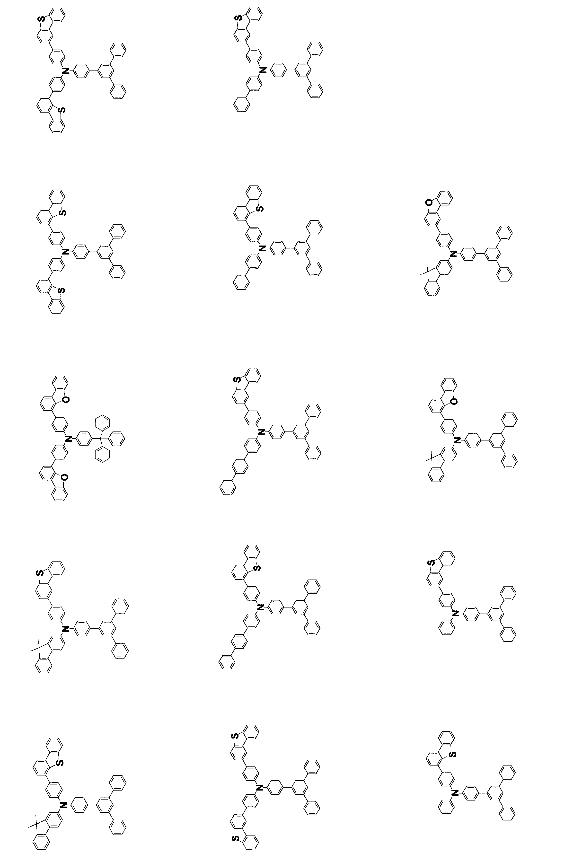

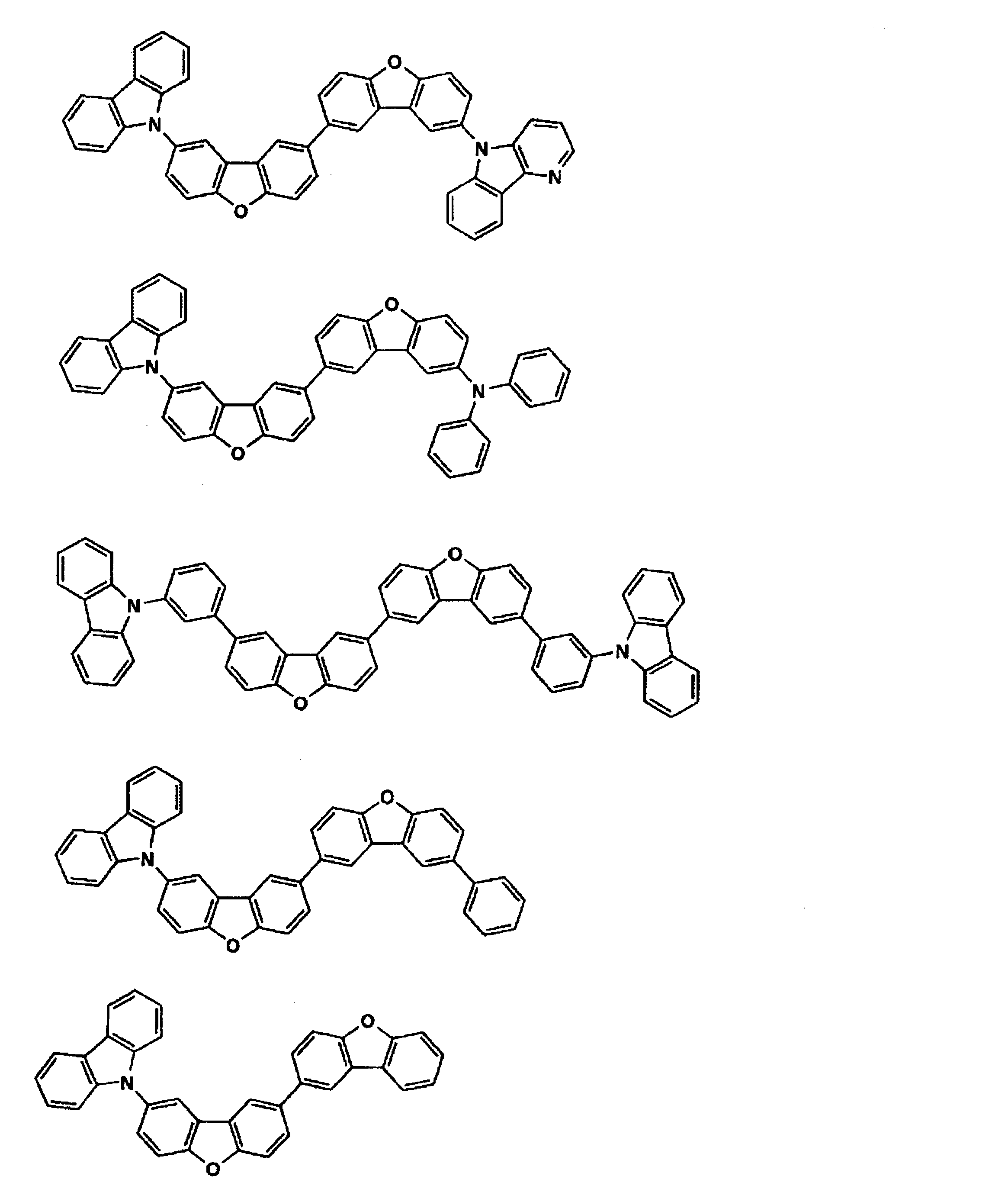


第1隣接層及び第2隣接層は、さらに後述する正孔注入輸送層の構成材料を含んでもよい。 The first adjacent layer and the second adjacent layer may include the adjacent layer compound described above, and preferably include substantially the adjacent layer compound, and more preferably include only the adjacent layer compound. Here, “substantially” means, for example, that the content of the adjacent layer compound is 90 wt% or more, 95 wt% or more, 98 wt% or more, or 99 wt% or more.
The first adjacent layer and the second adjacent layer may further include a constituent material of a hole injection transport layer described later.
第1隣接層及び第2隣接層の膜厚が同じである場合の当該膜厚は、例えば5nm~20nmであり、好ましくは、7~15nmである。
隣接層の膜厚が5nm未満の場合、隣接層が十分機能せず、第1の発光素子(例えば緑燐光発光素子、赤燐光発光素子)や第2の発光素子(例えば青蛍光発光素子)の効率や寿命が十分に得られないおそれがある。一方、隣接層の膜厚が20nm超の場合、発光素子が高電圧化し、キャリアバランスが悪くなり、結果的には、効率や寿命が十分に得られないおそれがある。 The first adjacent layer and the second adjacent layer are preferably the same film thickness. By making the film thickness of the first adjacent layer and the second adjacent layer the same, the first adjacent layer and the second adjacent layer can be simultaneously formed, and the manufacturing process of the organic EL multicolor light emitting device can be simplified. Cost reduction can be achieved.
When the film thickness of the first adjacent layer and the second adjacent layer is the same, the film thickness is, for example, 5 to 20 nm, and preferably 7 to 15 nm.
When the thickness of the adjacent layer is less than 5 nm, the adjacent layer does not function sufficiently, and the first light emitting element (for example, green phosphorescent light emitting element or red phosphorescent light emitting element) or the second light emitting element (for example, blue fluorescent light emitting element) There is a risk that sufficient efficiency and lifetime may not be obtained. On the other hand, when the film thickness of the adjacent layer is more than 20 nm, the voltage of the light emitting element is increased, the carrier balance is deteriorated, and as a result, there is a possibility that sufficient efficiency and lifetime may not be obtained.
第1発光層(例えば赤、黄燐光発光層、又は緑燐光発光層)と隣接する第1隣接層が、式(b)で表わされる置換基を有する化合物を含むことで、第1発光層側への電子輸送と注入の促進、及び赤、黄燐光層発光層又は緑燐光発光層からの三重項エネルギーの拡散を防止することができる。
第2発光層(例えば青蛍光発光層)と隣接する第2隣接層が、式(a)で表わされる置換基を有する化合物を含むことで、第2発光層への正孔輸送と注入を促進し、青発光の効率、寿命を高めることができる。 For the first adjacent layer and the second adjacent layer, preferably the first adjacent layer is adjacent to the first light-emitting layer and contains a compound having a substituent represented by formula (b), or the second adjacent layer is It includes a compound having a substituent represented by the formula (a) adjacent to the two light emitting layers.
When the first adjacent layer adjacent to the first light emitting layer (for example, red, yellow phosphorescent light emitting layer, or green phosphorescent light emitting layer) contains a compound having a substituent represented by the formula (b), the first light emitting layer side Facilitates electron transport and injection, and prevents triplet energy diffusion from the red, yellow, or green phosphorescent emitting layers.
The second adjacent layer adjacent to the second light emitting layer (for example, the blue fluorescent light emitting layer) contains a compound having a substituent represented by the formula (a), thereby promoting hole transport and injection to the second light emitting layer. In addition, the efficiency and life of blue light emission can be increased.
第1発光層(例えば赤、黄燐光発光層、又は緑燐光発光層)と隣接する第1隣接層が、(C)又は(D)の化合物を含むことで、第1発光層側への電子輸送と注入の促進、及び赤、黄燐光層発光層又は緑燐光発光層からの三重項エネルギーの拡散を防止することができる。
第2発光層(例えば青蛍光発光層)と隣接する第2隣接層が、(A)又は(B)の化合物を含むことで、第2発光層への正孔輸送と注入を促進し、青発光の効率、寿命を高めることができる。 In addition, for the first adjacent layer and the second adjacent layer, the first adjacent layer is preferably adjacent to the first light emitting layer, and includes the compound (C) or (D), or the second adjacent layer is the first adjacent layer. Two light emitting layers are adjacent to each other and contain the compound (A) or (B).
When the first adjacent layer adjacent to the first light emitting layer (for example, red, yellow phosphorescent light emitting layer, or green phosphorescent light emitting layer) contains the compound (C) or (D), electrons to the first light emitting layer side are obtained. Promotion of transport and injection, and diffusion of triplet energy from the red, yellow phosphorescent layer or green phosphorescent layer can be prevented.
The second adjacent layer adjacent to the second light-emitting layer (for example, the blue fluorescent light-emitting layer) contains the compound (A) or (B), thereby promoting hole transport and injection into the second light-emitting layer. The efficiency and life of light emission can be increased.
異なる2以上の層を積層した構成にするときは、例えば、上記のような2種以上の化合物から各層を形成し積層する。多層構成とするときは、多層の内、第1の発光素子の第1の有機層(第1発光層)に接する層を、他の層より三重項エネルギーの高い化合物((C)又は(D)の化合物、例えばカルバゾール部位とジベンゾフラン部位を有する化合物)で形成すると、第1の有機層(第1発光層)からの三重項エネルギーの拡散を防止することができ好ましい。
同様に、2種以上の化合物を用いて濃度勾配をつけて単層にするときは、三重項エネルギーがより高い化合物の濃度を、第1の発光素子の第1の有機層(第1発光層)側で高くすると好ましい。 The adjacent layer may have a single layer structure or a multilayer structure. When it is a single layer, it is formed from one or more compounds selected from the compounds (A) to (D). When two or more compounds are used, for example, two or more compounds having a substituent represented by formula (a), two or more compounds having a substituent represented by formula (b), or formula (a ) And a mixture of the compound represented by the formula (b). Moreover, you may change the density | concentration of 2 or more types of compounds within a layer.
When a configuration in which two or more different layers are laminated, for example, each layer is formed from two or more kinds of compounds as described above and laminated. In the case of a multi-layer structure, a layer in contact with the first organic layer (first light-emitting layer) of the first light-emitting element in the multilayer is a compound ((C) or (D ), Such as a compound having a carbazole moiety and a dibenzofuran moiety, is preferable because triplet energy diffusion from the first organic layer (first light-emitting layer) can be prevented.
Similarly, when two or more compounds are used to form a single layer with a concentration gradient, the concentration of the compound having a higher triplet energy is set to the first organic layer (first light-emitting layer) of the first light-emitting element. ) Side is preferable.
本発明の有機EL多色発光装置の基板上に並置されてなる第1の発光素子及び第2の発光素子について、第1の発光素子は例えば陽極/正孔注入層/正孔輸送層/第1発光層/第1隣接層/第2電子注入・輸送層/第1電子注入・輸送層/陰極で表わされる構造を有し、第2の発光素子は例えば陽極/正孔注入層/正孔輸送層/第2隣接層/第2発光層/第1電子注入・輸送層/陰極で表わされる構造を有する。
ここで、第1隣接層の材料と第2隣接層の材料は、それぞれ上記(A)~(D)の化合物のいずれかである。
また、第2発光層が青発光層の場合、第2発光層は、第1の発光素子の第2の電子注入・輸送層と同一でもよい。
第1発光層及び第2発光層の発光は、陽極側、陰極側、あるいは両側から取り出すことができる。 [Light emitting element]
Regarding the first light emitting element and the second light emitting element juxtaposed on the substrate of the organic EL multicolor light emitting device of the present invention, the first light emitting element is, for example, anode / hole injection layer / hole transport layer / second 1 light emitting layer / first adjacent layer / second electron injecting / transporting layer / first electron injecting / transporting layer / cathode. The second light emitting element is, for example, an anode / hole injecting layer / hole. It has a structure represented by transport layer / second adjacent layer / second light emitting layer / first electron injection / transport layer / cathode.
Here, the material of the first adjacent layer and the material of the second adjacent layer are each one of the compounds (A) to (D).
When the second light emitting layer is a blue light emitting layer, the second light emitting layer may be the same as the second electron injection / transport layer of the first light emitting element.
Light emission of the first light emitting layer and the second light emitting layer can be extracted from the anode side, the cathode side, or both sides.
発光層は、電子と正孔の再結合の場を提供し、これを発光につなげる機能を有する。
但し、発光層は、正孔の注入されやすさと電子の注入されやすさに違いがあってもよく、また、正孔と電子の移動度で表される輸送能に大小があってもよいが、どちらか一方の電荷を移動することが好ましい。 [Light emitting layer]
The light emitting layer has a function of providing a field for recombination of electrons and holes and connecting it to light emission.
However, the light emitting layer may have a difference in the ease of hole injection and the ease of electron injection, and the transport capability represented by the mobility of holes and electrons may be large or small. It is preferable to move one of the charges.
燐光ホストとしては、カルバゾール骨格と芳香族環又は含窒素芳香族環を同一分子内に含む化合物;複数のカルバゾ-ル骨格を同一分子内に含む化合物;芳香族環、縮合芳香族環及び含芳香族複素環を複数連結した化合物等が挙げられ、ホストは1種単独でも2種以上の混合物でもよい。 The first light emitting layer (corresponding to the first organic layer) contains a first light emitting dopant, preferably a phosphorescent dopant, and can function as a phosphorescent light emitting layer (for example, a red, yellow phosphorescent light emitting layer or a green phosphorescent light emitting layer). The phosphorescent light emitting layer is preferably a phosphorescent light emitting layer containing a phosphorescent host and a phosphorescent dopant.
The phosphorescent host includes a compound containing a carbazole skeleton and an aromatic ring or a nitrogen-containing aromatic ring in the same molecule; a compound containing a plurality of carbazole skeletons in the same molecule; an aromatic ring, a condensed aromatic ring and an aromatic ring A compound in which a plurality of group heterocycles are linked, and the host may be a single type or a mixture of two or more types.
燐光量子収率が高く、発光素子の外部量子効率をより向上させることができるという点で、燐光ドーパントは、Ir,Os及びPtから選ばれる金属原子を含有する化合物であると好ましく、イリジウム錯体、オスミウム錯体、白金錯体等の金属錯体であるとさらに好ましく、中でもイリジウム錯体及び白金錯体がより好ましく、オルトメタル化イリジウム錯体が最も好ましい。ドーパントは、1種単独でも、2種以上の混合物でもよい。
第1発光層は、隣接層化合物、正孔輸送材、電子輸送材も必要に応じて含んでもよい。 Examples of phosphorescent dopants include metal complex compounds, which are preferably compounds having a metal atom selected from Ir, Pt, Os, Au, Cu, Re and Ru and a ligand. . The ligand preferably has an ortho metal bond.
The phosphorescent dopant is preferably a compound containing a metal atom selected from Ir, Os and Pt in that the phosphorescent quantum yield is high and the external quantum efficiency of the light-emitting element can be further improved, and an iridium complex, It is more preferable that it is a metal complex such as an osmium complex or a platinum complex, among which an iridium complex and a platinum complex are more preferable, and an orthometalated iridium complex is most preferable. The dopant may be a single type or a mixture of two or more types.
The first light emitting layer may also include an adjacent layer compound, a hole transport material, and an electron transport material as necessary.
蛍光ホストとしては、各種縮合芳香族環化合物が挙げられ、例えば下記(2)~(12)で表わされる化合物から選択される1以上を用いることができる。


Examples of the fluorescent host include various condensed aromatic ring compounds. For example, one or more selected from the compounds represented by the following (2) to (12) can be used.
aは0~7の整数であり、bは0~9の整数であり、cは0~11の整数であり、dは0~22の整数であり、fは0~18の整数であり、a~fのそれぞれが2以上の場合、複数のRは互いに同一でも、異なっていてもよい。
上記アリール基、複素環基及びアルキル基は、隣接層化合物のAr1~Ar4の置換もしくは無置換の芳香族炭化水素基、置換もしくは無置換の芳香族複素環基及び置換もしくは無置換のアルキル基と同様である。
上記式(2)~(12)において、Rはいずれの芳香族環又は複素環に結合していてもよく、また、2以上のRが同一の芳香族環又は複素環に結合していてもよい。) Wherein R is a substituted or unsubstituted aryl group having 6 to 40 ring carbon atoms (preferably a substituted or unsubstituted aryl group having 6 to 18 ring carbon atoms), or a substituted or unsubstituted ring atom number. A heterocyclic group having 3 to 40 (preferably a substituted or unsubstituted heterocyclic group having 3 to 18 ring atoms), or a substituted or unsubstituted alkyl group having 1 to 50 carbon atoms (preferably substituted or unsubstituted) And an alkyl group having 1 to 20 carbon atoms.
a is an integer from 0 to 7, b is an integer from 0 to 9, c is an integer from 0 to 11, d is an integer from 0 to 22, and f is an integer from 0 to 18, When each of a to f is 2 or more, the plurality of R may be the same as or different from each other.
The aryl group, heterocyclic group and alkyl group are the substituted or unsubstituted aromatic hydrocarbon group, substituted or unsubstituted aromatic heterocyclic group and substituted or unsubstituted alkyl of Ar 1 to Ar 4 in the adjacent layer compound. Same as the group.
In the above formulas (2) to (12), R may be bonded to any aromatic ring or heterocyclic ring, or two or more R may be bonded to the same aromatic ring or heterocyclic ring. Good. )

Xは、置換もしくは無置換の環形成炭素数10~40の1+s価の縮合芳香族環基、置換もしくは無置換の1+s価のスチリル基である。
sは0~3の整数であり、sが2又は3である場合、2又は3個の-NAr3Ar4は同一でも異なっていてもよく、sが0の場合-NAr3Ar4は水素原子を表す。) As the fluorescent dopant, aromatic amines represented by the following formula, styrylamine represented by the following formula, and the like are preferable. The fluorescent dopant may be a single type or a mixture of two or more types.
X is a substituted or unsubstituted 1 + s-valent condensed aromatic ring group having 10 to 40 ring carbon atoms and a substituted or unsubstituted 1 + s-valent styryl group.
s is an integer of 0 to 3, and when s is 2 or 3, 2 or 3 —NAr 3 Ar 4 may be the same or different, and when s is 0, —NAr 3 Ar 4 is hydrogen Represents an atom. )
基板としてはガラス板、ポリマー板等を用いることができる。
ガラス板としては、特にソーダ石灰ガラス、バリウム・ストロンチウム含有ガラス、鉛ガラス、アルミノケイ酸ガラス、ホウケイ酸ガラス、バリウムホウケイ酸ガラス、石英等が挙げられる。また、ポリマー板としては、ポリカーボネート、アクリル、ポリエチレンテレフタレート、ポリエーテルサルフォン、ポリサルフォン等を挙げることができる。 [substrate]
As the substrate, a glass plate, a polymer plate or the like can be used.
Examples of the glass plate include soda lime glass, barium / strontium-containing glass, lead glass, aluminosilicate glass, borosilicate glass, barium borosilicate glass, and quartz. Examples of the polymer plate include polycarbonate, acrylic, polyethylene terephthalate, polyethersulfone, and polysulfone.
陽極は例えば導電性材料からなり、4eVより大きな仕事関数を有する導電性材料が適している。
上記導電性材料としては、炭素、アルミニウム、バナジウム、鉄、コバルト、ニッケル、タングステン、銀、金、白金、パラジウム等及びそれらの合金、ITO基板、NESA基板に使用される酸化スズ、酸化インジウム等の酸化金属、さらにはポリチオフェンやポリピロール等の有機導電性樹脂が挙げられる。
陽極は、必要があれば2層以上の層構成により形成されていてもよい。 [anode]
The anode is made of, for example, a conductive material, and a conductive material having a work function larger than 4 eV is suitable.
Examples of the conductive material include carbon, aluminum, vanadium, iron, cobalt, nickel, tungsten, silver, gold, platinum, palladium, and their alloys, ITO substrate, tin oxide used for NESA substrate, indium oxide, and the like. Examples thereof include metal oxides and organic conductive resins such as polythiophene and polypyrrole.
The anode may be formed with a layer structure of two or more layers if necessary.
陰極は例えば導電性材料からなり、4eVより小さな仕事関数を有する導電性材料が適している。
上記導電性材料としては、マグネシウム、カルシウム、錫、鉛、チタニウム、イットリウム、リチウム、ルテニウム、マンガン、アルミニウム、フッ化リチウム等及びこれらの合金が挙げられるが、これらに限定されるものではない。
また、上記合金としては、マグネシウム/銀、マグネシウム/インジウム、リチウム/アルミニウム等が代表例として挙げられるが、これらに限定されるものではない。合金の比率は、蒸着源の温度、雰囲気、真空度等により制御され、適切な比率に選択される。
陰極は、必要があれば2層以上の層構成により形成されていてもよく、陰極は上記導電性材料を蒸着やスパッタリング等の方法により薄膜を形成させることにより、作製することができる。 [cathode]
The cathode is made of, for example, a conductive material, and a conductive material having a work function smaller than 4 eV is suitable.
Examples of the conductive material include, but are not limited to, magnesium, calcium, tin, lead, titanium, yttrium, lithium, ruthenium, manganese, aluminum, lithium fluoride, and alloys thereof.
Examples of the alloy include magnesium / silver, magnesium / indium, lithium / aluminum, and the like, but are not limited thereto. The ratio of the alloy is controlled by the temperature of the vapor deposition source, the atmosphere, the degree of vacuum, etc., and is selected to an appropriate ratio.
If necessary, the cathode may be formed with a layer structure of two or more layers, and the cathode can be produced by forming a thin film from the conductive material by a method such as vapor deposition or sputtering.
また、陰極としてのシート抵抗は数百Ω/□以下が好ましく、膜厚は通常10nm~1μmであり、好ましくは50~200nmである。 When light emitted from the light emitting layer is taken out from the cathode, the transmittance of the cathode for light emission is preferably greater than 10%.
The sheet resistance as the cathode is preferably several hundred Ω / □ or less, and the film thickness is usually 10 nm to 1 μm, preferably 50 to 200 nm.
正孔注入・輸送層は、発光層への正孔注入を助け、発光領域まで輸送する層であって、正孔移動度が大きく、イオン化エネルギーが通常5.6eV以下と小さい層である。
正孔注入・輸送層の材料としては、より低い電界強度で正孔を発光層に輸送する材料が好ましく、さらに正孔の移動度が、例えば104~106V/cmの電界印加時に、少なくとも10-4cm2/V・秒であれば好ましい。 [Hole injection layer and hole transport layer]
The hole injection / transport layer is a layer that assists hole injection into the light emitting layer and transports it to the light emitting region, and has a high hole mobility and a small ionization energy of usually 5.6 eV or less.
As the material for the hole injection / transport layer, a material that transports holes to the light emitting layer with a lower electric field strength is preferable. Further, when a hole mobility is, for example, 10 4 to 10 6 V / cm, It is preferably at least 10 −4 cm 2 / V · sec.
また、p型Si、p型SiC等の無機化合物も正孔注入材料として使用することができる。 Specific examples of the material for the hole injection / transport layer include triazole derivatives (see US Pat. No. 3,112,197) and oxadiazole derivatives (see US Pat. No. 3,189,447). ), Imidazole derivatives (see JP-B-37-16096, etc.), polyarylalkane derivatives (US Pat. Nos. 3,615,402, 3,820,989, 3,542,544) Nos. 45-555, 51-10983, 51-93224, 55-17105, 56-4148, 55-108667, 55-156953, 56-36656, etc.), pyrazoline derivatives and pyrazolone derivatives (US Pat. No. 3,180,729, No. 4) 278,746, JP 55-88064, 55-88065, 49-105537, 55-51086, 56-80051, 56-88141. No. 57-45545, No. 54-112537, No. 55-74546, etc.), phenylenediamine derivatives (US Pat. No. 3,615,404, JP-B 51-10105, 46-3712, 47-25336, JP 54-53435, 54-110536, 54-1119925, etc.), arylamine derivatives (US Pat. No. 3,567) , 450 specification, 3,180,703 specification, 3,240,597 specification, 3,658,520 specification. No. 4,232,103, No. 4,175,961, No. 4,012,376, JP-B-49-35702, JP-A-39-27577, Nos. 55-144250, 56-119132, 56-22437, West German Patent 1,110,518, etc.), amino-substituted chalcone derivatives (US Pat. No. 3,526,501) Oxazole derivatives (disclosed in US Pat. No. 3,257,203, etc.), styryl anthracene derivatives (see JP 56-46234 A, etc.), fluorenone derivatives (JP No. 54-110837), hydrazone derivatives (US Pat. No. 3,717,462, JP-A-54-59143, 55-52063). No. 55-52064, No. 55-46760, No. 55-85495, No. 57-11350, No. 57-148749, JP-A-2-311591, etc.), stilbene derivatives (Japanese Patent Laid-Open Nos. 61-210363, 61-228451, 61-14642, 61-72255, 62-47646, 62-36674, 62-10652) No. 6, No. 62-30255, No. 60-93455, No. 60-94462, No. 60-174749, No. 60-175052, etc., silazane derivatives (US Pat. No. 4,950) , 950 specification), polysilane (JP-A-2-204996), aniline-based copolymer (JP-A-2-2822). 63) and conductive polymer oligomers (particularly thiophene oligomers) disclosed in JP-A No. 1-211399.
In addition, inorganic compounds such as p-type Si and p-type SiC can also be used as the hole injection material.
電子注入・輸送層は、発光層への電子の注入を助け、発光領域まで輸送する層であって、電子移動度が大きい層である。
有機EL素子は発光した光が電極(例えば陰極)により反射するため、直接陽極から取り出される発光と、電極による反射を経由して取り出される発光とが干渉することが知られている。この干渉効果を効率的に利用するため、電子注入・輸送層は数nm~数μmの膜厚で適宜選ばれるが、特に膜厚が厚いとき、電圧上昇を避けるために、104~106V/cmの電界印加時に電子移動度が少なくとも10-5cm2/Vs以上であることが好ましい。 [Electron injection layer and electron transport layer]
The electron injecting / transporting layer is a layer that assists the injection of electrons into the light emitting layer and transports it to the light emitting region, and has a high electron mobility.
In the organic EL element, since emitted light is reflected by an electrode (for example, a cathode), it is known that light emitted directly from the anode interferes with light emitted via reflection by the electrode. To efficiently utilize the interference, although the electron injecting and transporting layer is suitably selected in a film thickness of several nm ~ number [mu] m, especially when thick film thickness, in order to avoid a voltage rise, 10 4 to 10 6 The electron mobility is preferably at least 10 −5 cm 2 / Vs or more when an electric field of V / cm is applied.
本発明の有機EL多色発光装置における層間絶縁膜は、主に、各発光素子(発光層)を分離することを目的に用いられるが、その他、高精細な電極のエッジの平坦化、有機EL素子の下部電極と上部電極との間の電気絶縁(短絡防止)に用いられる。
層間絶縁膜に用いられる構成材料としては、通常、アクリル樹脂、ポリカーボネート樹脂、ポリイミド樹脂等の有機材料、酸化ケイ素(SiO2又はSiOx)、酸化アルミニウム(Al2O3又はAlOx)、酸化チタン(TiO2)、窒化シリコン(Si3N4)、窒化シリコン酸化物(SiOxNy)等の無機酸化物が挙げられる。
層間絶縁膜は、上記構成材料に感光性基を導入してフォトリソグラフィー法で所望のパターンに加工するか、印刷手法にて所望のパターンに形成することが好ましい。 [Interlayer insulation film]
The interlayer insulating film in the organic EL multicolor light emitting device of the present invention is mainly used for the purpose of separating each light emitting element (light emitting layer). Used for electrical insulation (short circuit prevention) between the lower electrode and the upper electrode of the element.
As the constituent material used for the interlayer insulating film, organic materials such as acrylic resin, polycarbonate resin, polyimide resin, silicon oxide (SiO 2 or SiOx), aluminum oxide (Al 2 O 3 or AlOx), titanium oxide (TiO 2 ) are usually used. 2 ), inorganic oxides such as silicon nitride (Si 3 N 4 ) and silicon nitride oxide (SiOxNy).
The interlayer insulating film is preferably formed into a desired pattern by a photolithographic method by introducing a photosensitive group into the constituent material or by a printing method.
本発明の有機EL多色発光装置の各層の形成は、真空蒸着、スパッタリング、プラズマ、イオンプレーティング等の公知の乾式成膜法やスピンコート法、キャスティング法、マイクログラビアコート法、グラビアコート法、バーコート法、ロールコート法、スリットコート法、ワイアーバーコート法、ディップコート法、スプレーコート法、スクリーン印刷法、フレキソ印刷法、オフセット印刷法、インクジェット法、ノズルプリンティング法等の公知の湿式成膜法を適用することができ、パターン形成をする場合には、スクリーン印刷法、フレキソ印刷法、オフセット印刷法、インクジェット印刷法等の方法を適用することができる。
各層の膜厚は特に限定されるものではないが、適切な膜厚に設定する必要がある。膜厚が厚すぎると、一定の光出力を得るために大きな印加電圧が必要になり効率が悪くなる。膜厚が薄すぎるとピンホール等が発生して、電界を印加しても充分な発光輝度が得られない。通常の膜厚は5nm~10μmの範囲が適しているが、10nm~0.2μmの範囲がさらに好ましい。 [Method for Manufacturing Organic EL Multicolor Light Emitting Device]
The formation of each layer of the organic EL multicolor light emitting device of the present invention is performed by a known dry film forming method such as vacuum deposition, sputtering, plasma, ion plating, spin coating method, casting method, micro gravure coating method, gravure coating method, Known wet film formation such as bar coating method, roll coating method, slit coating method, wire bar coating method, dip coating method, spray coating method, screen printing method, flexographic printing method, offset printing method, ink jet method, nozzle printing method, etc. A method such as a screen printing method, a flexographic printing method, an offset printing method, and an ink jet printing method can be applied.
The thickness of each layer is not particularly limited, but needs to be set to an appropriate thickness. If the film thickness is too thick, a large applied voltage is required to obtain a constant light output, resulting in poor efficiency. If the film thickness is too thin, pinholes and the like are generated, and sufficient light emission luminance cannot be obtained even when an electric field is applied. The normal film thickness is suitably in the range of 5 nm to 10 μm, more preferably in the range of 10 nm to 0.2 μm.
成膜後、真空、加熱乾燥して、溶媒を除去すればよく、光、高温(200℃以上)加熱による重合反応は不要である。従って、光、高温加熱による性能劣化は抑制される。 For example, as a method for forming the hole injection / transport layer, film formation using a solution containing an aromatic amine derivative can be mentioned. Film formation methods include spin coating, casting, micro gravure coating, gravure coating, bar coating, roll coating, slit coating, wire bar coating, dip coating, spray coating, and screen printing. , Flexographic printing method, offset printing method, ink jet method, nozzle printing method, and the like. In the case of pattern formation, screen printing method, flexographic printing method, offset printing method, and ink jet printing method are preferable. Film formation by these methods can be performed under conditions well known to those skilled in the art.
After the film formation, the solvent may be removed by vacuum and heat drying, and the polymerization reaction by light and high temperature (200 ° C. or higher) heating is unnecessary. Therefore, performance degradation due to light and high temperature heating is suppressed.
成膜用溶液中の芳香族アミン誘導体の含有量は、溶媒を除いた組成物の全重量に対して好ましくは20~100重量%であり、より好ましくは51~100重量%であり、溶媒を除いた組成物の主成分であるとよい。溶媒の割合は、成膜用溶液の1~99.9重量%が好ましく、80~99重量%がより好ましい。
尚、「主成分」とは、芳香族アミン誘導体の含有量が50質量%以上であることを意味する。 The hole injecting / transporting layer film forming solution only needs to contain at least one aromatic amine derivative, and in addition to the aromatic amine derivative, other hole transporting materials, electron transporting materials, light emitting materials, acceptor materials In addition, additives such as a solvent and a stabilizer may be included.
The content of the aromatic amine derivative in the film-forming solution is preferably 20 to 100% by weight, more preferably 51 to 100% by weight, based on the total weight of the composition excluding the solvent. It may be the main component of the removed composition. The proportion of the solvent is preferably 1 to 99.9% by weight of the film-forming solution, and more preferably 80 to 99% by weight.
The “main component” means that the content of the aromatic amine derivative is 50% by mass or more.
これらのうち、溶解性、成膜の均一性、粘度特性等の観点から、芳香族炭化水素系溶媒、エーテル系溶媒、脂肪族炭化水素系溶媒、エステル系溶媒、ケトン系溶媒が好ましく、トルエン、キシレン、エチルベンゼン、ジエチルベンゼン、トリメチルベンゼン、n-プロピルベンゼン、イソプロピルベンゼン、n-ブチルベンゼン、イソブチルベンゼン、5-ブチルベンゼン、n-へキシルベンゼン、シクロへキシルベンゼン、1-メチルナフタレン、テトラリン、1,3-ジオキサン、1,4-ジオキサン、1,3-ジオキソラン、アニソール、エトキシベンゼン、シクロへキサン、ビシクロへキシル、シクロヘキセニルシクロヘキサノン、n-ヘプチルシクロへキサン、n-へキシルシクロヘキサン、デカリン、安息香酸メチル、シクロへキサノン、2-プロピルシクロへキサノン、2-へプタノン、3-へプタノン、4-へプタノン、2-オクタノン、2-ノナノン、2-デカノン、ジシクロへキシルケトン、アセトフェノン、ベンゾフェノンが好ましい。 Examples of the solvent for the film forming solution include chlorine solvents such as chloroform, methylene chloride, 1,2-dichloroethane, 1,1,2-trichloroethane, chlorobenzene, o-dichlorobenzene, ethers such as tetrahydrofuran, dioxane, dioxolane, and anisole. Solvents; aromatic hydrocarbon solvents such as toluene and xylene; cyclohexane, methylcyclohexane, n-pentane, n-hexane, n-heptane, n-octane, n-nonane, n-decane, etc. Aliphatic hydrocarbon solvents; Ketone solvents such as acetone, methyl ethyl ketone, cyclohexanone, benzophenone, and acetophenone; Ester solvents such as ethyl acetate, butyl acetate, ethyl cellosolve acetate, methyl benzoate, and phenyl acetate; ethylene glycol , Ethylene glycol monobutyl Ethers, ethylene glycol monoethyl ether, ethylene glycol monomethyl ether, dimethoxyethane, propylene glycol, diethoxymethane, triethylene glycol monoethyl ether, glycerin, 1,2-hexanediol and other polyhydric alcohols and derivatives thereof; methanol, Examples include alcohol solvents such as ethanol, propanol, isopropanol, and cyclohexanol; sulfoxide solvents such as dimethyl sulfoxide; amide solvents such as N-methyl-2-pyrrolidone and N, N-dimethylformamide. These organic solvents can be used alone or in combination.
Of these, aromatic hydrocarbon solvents, ether solvents, aliphatic hydrocarbon solvents, ester solvents, ketone solvents are preferred from the viewpoints of solubility, film formation uniformity, viscosity characteristics, etc., toluene, Xylene, ethylbenzene, diethylbenzene, trimethylbenzene, n-propylbenzene, isopropylbenzene, n-butylbenzene, isobutylbenzene, 5-butylbenzene, n-hexylbenzene, cyclohexylbenzene, 1-methylnaphthalene, tetralin, 1, 3-dioxane, 1,4-dioxane, 1,3-dioxolane, anisole, ethoxybenzene, cyclohexane, bicyclohexyl, cyclohexenylcyclohexanone, n-heptylcyclohexane, n-hexylcyclohexane, decalin, benzoic acid Methyl to cyclo Sanon, cyclohexanone to 2-propylcyclopentadienyl, heptanone to 2, heptanone to 3, heptanone to 4, 2-octanone, 2-nonanone, 2-decanone, Kishiruketon dicyclohexyl, acetophenone, benzophenone is preferable.
特に本発明の有機EL多色発光装置では、隣接層化合物が塗布層と蒸着層の境界にあるハイブリッドコネクティングレイヤー(HCL)に適した有機EL材料であり、低コストで大画面化可能な塗布層と高性能な蒸着層を組み合わせたハイブリッド型有機EL多色発光装置とすることができる。 By the various materials and layer forming methods exemplified above, for example, the structure of anode / hole injection layer / hole transport layer / first light emitting layer / first adjacent layer / second electron transport layer / first electron transport layer / cathode is obtained. A second light-emitting element having a structure of anode / hole injection layer / hole transport layer / second adjacent layer / second light-emitting layer / first electron transport layer / cathode, for example. The organic EL multicolor light emitting device of the present invention can be manufactured. Moreover, an organic EL element can also be produced from the cathode to the anode in the reverse order. In addition, the hole injection layer and the hole transport layer are not limited to a structure formed by stacking two different layers, and can be formed in one layer using a material that functions as a hole injection transport layer.
In particular, the organic EL multicolor light emitting device of the present invention is an organic EL material suitable for a hybrid connecting layer (HCL) in which the adjacent layer compound is at the boundary between the coating layer and the vapor deposition layer, and can be applied at a low cost and with a large screen. And a hybrid organic EL multicolor light emitting device combining a high-performance vapor deposition layer.


(1)三重項エネルギー(T1)
三重項エネルギーは、市販の装置F-4500(株式会社日立ハイテクノロジーズ製)を用いて測定した。T1の換算式は以下の通りである。
換算式 T1(eV)=1239.85/λedge
尚、λedge(単位:nm)とは、縦軸にリン光強度、横軸に波長をとって、リン光スペクトルを表したときに、リン光スペクトルの短波長側の立ち上がりに対して接線を引き、その接線と横軸の交点の波長値を意味する。 The triplet energy T1, singlet energy S1, ionization potential IP, and electron affinity Af of the above compounds 1 to 4, 8 to 12, 14 to 28, and A to C were measured by the following methods. The results are shown in Table 1.
(1) Triplet energy (T1)
Triplet energy was measured using a commercially available apparatus F-4500 (manufactured by Hitachi High-Technologies Corporation). The conversion formula for T1 is as follows.
Conversion formula T1 (eV) = 1239.85 / λ edge
Note that λ edge (unit: nm) is a tangent to the rising edge of the phosphorescence spectrum on the short wavelength side when the phosphorescence spectrum is represented by taking the phosphorescence intensity on the vertical axis and the wavelength on the horizontal axis. It means the wavelength value at the intersection of the tangent and the horizontal axis.
イオン化ポテンシャルは、大気下で光電子分光装置(理研計器(株)社製:AC-3)を用いて測定した。具体的には、材料に光を照射し、その際に電荷分離によって生じる電子量を測定することにより測定した。
尚、イオン化ポテンシャル(Ip)は、ホスト材料の化合物から電子を取り去ってイオン化するために要するエネルギーを意味する。 (2) Ionization potential (IP)
The ionization potential was measured in the atmosphere using a photoelectron spectrometer (manufactured by Riken Keiki Co., Ltd .: AC-3). Specifically, the measurement was performed by irradiating the material with light and measuring the amount of electrons generated by charge separation at that time.
The ionization potential (Ip) means the energy required for removing electrons from the host material compound and ionizing.
イオン化ポテンシャルIpと一重項エネルギー(S1:Eg)の測定値からアフィニティを算出した。算出式は、次の通りである。
Af=Ip-Eg
一重項エネルギー(S1:Eg)は、最低励起一重項状態と基底状態のエネルギー差をいい、ベンゼン中の吸収スペクトルの吸収端から測定した。具体的には、市販の可視・紫外分光光度計を用いて、吸収スペクトルを測定し、そのスペクトルが立ち上がり始める波長から算出した。
尚、アフィニティー(Af、電子親和力)とは、ホスト材料の分子に電子を1つ与えた時に放出又は吸収されるエネルギーをいい、放出の場合は正、吸収の場合は負と定義する。 (3) Affinity (Af)
The affinity was calculated from the measured values of ionization potential Ip and singlet energy (S1: Eg). The calculation formula is as follows.
Af = Ip-Eg
Singlet energy (S1: Eg) is the energy difference between the lowest excited singlet state and the ground state, and was measured from the absorption edge of the absorption spectrum in benzene. Specifically, the absorption spectrum was measured using a commercially available visible / ultraviolet spectrophotometer, and calculated from the wavelength at which the spectrum started rising.
Affinity (Af, electron affinity) refers to the energy released or absorbed when one electron is given to the molecule of the host material, and is defined as positive in the case of emission and negative in the case of absorption.

本発明の有機EL多色発光装置の効果を確認するため、第1の発光素子と第2の発光素子を評価した。
[第2の発光素子(青色蛍光発光素子)の形成]
25mm×75mm×1.1mm厚のITO透明電極付きガラス基板を、イソプロピルアルコール中で5分間超音波洗浄した後、UVオゾン洗浄を30分間行なった。洗浄後の透明電極付きガラス基板に、ND1501(日産化学工業製:アニリンオリゴマー)をスピンコート法で25nmの膜厚で成膜して、230℃で加熱して正孔注入層を形成した。ついで、HT1のキシレン溶液(1.0重量%)を、スピンコート法で30nmの膜厚で成膜し、120℃で乾燥し、正孔輸送層を形成した。次に、第2の隣接層(第2の有機層)の材料として化合物1を蒸着により、膜厚10nmに成膜した。次に第2の発光層(青発光層)(第3の有機層)として、ホスト材EM1とドーパント材BD1を97:3の質量比で蒸着し、膜厚35nmの発光層を形成した。さらに、ET1を蒸着により、膜厚25nmに成膜した。この層は、電子輸送層として機能する。この後、還元性ドーパントであるLi(Li源:サエスゲッター社製)とAlqを2元蒸着させ、電子注入層としてAlq:Li膜(膜厚10nm)を形成した。このAlq:Li膜上に金属Alを蒸着させ金属陰極を形成し、窒素中でガラス封止して、第2の発光素子である青色発光有機EL素子を作製した。 Example 1
In order to confirm the effect of the organic EL multicolor light emitting device of the present invention, the first light emitting element and the second light emitting element were evaluated.
[Formation of Second Light Emitting Element (Blue Fluorescent Light Emitting Element)]
A glass substrate with an ITO transparent electrode having a thickness of 25 mm × 75 mm × 1.1 mm was ultrasonically cleaned in isopropyl alcohol for 5 minutes, and then UV ozone cleaning was performed for 30 minutes. On the glass substrate with a transparent electrode after washing, ND1501 (Nissan Chemical Industries: aniline oligomer) was formed into a film with a thickness of 25 nm by a spin coating method, and heated at 230 ° C. to form a hole injection layer. Next, a xylene solution of HT1 (1.0% by weight) was formed into a film having a thickness of 30 nm by a spin coating method and dried at 120 ° C. to form a hole transport layer. Next, Compound 1 was deposited to a thickness of 10 nm as a material for the second adjacent layer (second organic layer) by vapor deposition. Next, as a second light emitting layer (blue light emitting layer) (third organic layer), a host material EM1 and a dopant material BD1 were deposited at a mass ratio of 97: 3 to form a light emitting layer having a thickness of 35 nm. Further, ET1 was deposited to a film thickness of 25 nm by vapor deposition. This layer functions as an electron transport layer. Thereafter, Li (Li source: manufactured by SAES Getter Co., Ltd.), which is a reducing dopant, and Alq were vapor-deposited to form an Alq: Li film (film thickness: 10 nm) as an electron injection layer. A metal cathode was formed by vapor-depositing metal Al on this Alq: Li film, and glass sealing was performed in nitrogen to produce a blue light-emitting organic EL device as a second light-emitting device.
25mm×75mm×1.1mm厚のITO透明電極付きガラス基板を、イソプロピルアルコール中で5分間超音波洗浄した後、UVオゾン洗浄を30分間行なった。洗浄後の透明電極付きガラス基板に、ND1501(日産化学工業製)をスピンコート法で25nmの膜厚で成膜して、230℃で加熱して正孔注入層を形成した。ついで、WO2009/102027に開示のHT2のキシレン溶液(1.0重量%)を、スピンコート法で30nmの膜厚で成膜し、230℃で加熱乾燥して、正孔輸送層を形成した。次に、第1発光層(緑発光層)(第1の有機層)として、ホスト材EM2とドーパント材GD1の90:10の重量比のキシレン溶液(1.0重量%)を調製し、スピンコート法で60nmの膜厚で成膜し、120℃で乾燥した。次に、第1隣接層(第2の有機層)の材料として第2隣接層の材料と同じ化合物1を蒸着により、膜厚10nmに成膜した。次に、ホスト材EM1とドーパント材BD1を97:3のレート比で蒸着し、膜厚35nmの層(青共通層)(第3の有機層)を形成し、次に、ET1を蒸着により、膜厚25nmに成膜した。これら層は、電子輸送層として機能する。この後、還元性ドーパントであるLi(Li源:サエスゲッター社製)とAlqを二元蒸着させ、電子注入層としてAlq:Li膜(膜厚10nm)を形成した。このAlq:Li膜上に金属Alを蒸着させ金属陰極を形成し、窒素中でガラス封止して、第1の発光素子である緑色発光有機EL素子を作製した。 [Production of First Light-Emitting Element (Green Phosphorescent Light-Emitting Element)]
A glass substrate with an ITO transparent electrode having a thickness of 25 mm × 75 mm × 1.1 mm was ultrasonically cleaned in isopropyl alcohol for 5 minutes, and then UV ozone cleaning was performed for 30 minutes. ND1501 (manufactured by Nissan Chemical Industries, Ltd.) was formed into a film thickness of 25 nm by spin coating on the glass substrate with a transparent electrode after washing, and heated at 230 ° C. to form a hole injection layer. Next, a xylene solution of HT2 (1.0% by weight) disclosed in WO2009 / 102027 was formed into a film having a thickness of 30 nm by a spin coating method, and heated and dried at 230 ° C. to form a hole transport layer. Next, a 90:10 weight ratio xylene solution (1.0 wt%) of the host material EM2 and the dopant material GD1 is prepared as a first light emitting layer (green light emitting layer) (first organic layer), and spin A film having a film thickness of 60 nm was formed by a coating method and dried at 120 ° C. Next, the same compound 1 as the material of the second adjacent layer was deposited as a material of the first adjacent layer (second organic layer) to a thickness of 10 nm by vapor deposition. Next, the host material EM1 and the dopant material BD1 are vapor-deposited at a rate ratio of 97: 3 to form a 35 nm-thick layer (blue common layer) (third organic layer), and then ET1 is vapor-deposited. The film was formed to a film thickness of 25 nm. These layers function as an electron transport layer. Thereafter, Li (Li source: manufactured by SAES Getter), which is a reducing dopant, and Alq were vapor-deposited to form an Alq: Li film (film thickness: 10 nm) as an electron injection layer. Metal Al was vapor-deposited on the Alq: Li film to form a metal cathode, and glass sealing was performed in nitrogen to produce a green light-emitting organic EL element as a first light-emitting element.
化合物1からなる第1隣接層及び第2隣接層の代わりに、表2に示す化合物8~12、14~18をそれぞれ単層で蒸着した隣接層を採用した他は実施例1と同様にして第1の発光素子及び第2の発光素子を製造し評価した。結果を表2に示す。 Examples 2 to 11
Instead of the first adjacent layer and the second adjacent layer made of Compound 1, the same procedure as in Example 1 was adopted except that adjacent layers in which the
化合物1からなる第1隣接層及び第2隣接層の代わりに、それぞれ化合物2を5nmで蒸着し、次いで化合物1を5nmで蒸着した隣接層を採用した他は実施例1と同様にして第1の発光素子及び第2の発光素子を製造し評価した。結果を表2に示す。 Example 12
Instead of the first adjacent layer and the second adjacent layer made of compound 1, compound 2 was deposited at 5 nm, respectively, and then the adjacent layer formed by depositing compound 1 at 5 nm was used. The light emitting device and the second light emitting device were manufactured and evaluated. The results are shown in Table 2.
実施例12において化合物1,2を用いて第1隣接層及び第2隣接層を形成する代わりに、表2に示す化合物を用いて第1隣接層及び第2隣接層を形成した他は、実施例12と同様にして第1の発光素子及び第2の発光素子を製造し評価した。結果を表2に示す。 Examples 13-54
In Example 12, instead of forming the first adjacent layer and the second adjacent layer using the compounds 1 and 2, the compounds shown in Table 2 were used to form the first adjacent layer and the second adjacent layer. The first light-emitting element and the second light-emitting element were manufactured and evaluated in the same manner as in Example 12. The results are shown in Table 2.
実施例1の化合物1の代わりに表2に示す化合物(A~C)を用いて、それぞれ単層の第1隣接層及び第2隣接層を形成した他は実施例1と同様にして、第1の発光素子及び第2の発光素子を製造し評価した。結果を表2に示す。 Comparative Examples 1 to 3
In the same manner as in Example 1, except that the compounds (A to C) shown in Table 2 were used instead of Compound 1 of Example 1 to form a single first adjacent layer and a second adjacent layer, respectively. The first light emitting device and the second light emitting device were manufactured and evaluated. The results are shown in Table 2.


また、第2の発光素子(青)の寿命は良好である。これは、アミンユニットまたはカルバゾールユニットに加えて、耐電子性の高いジベンゾフランユニットを有するためと推定される。 In Examples 1 to 11 in which the adjacent layer was composed of a single layer, compounds 1, 8 to 12, and 14 to 18 were used. These compounds contain an arylamine moiety and a dibenzofuran moiety, or a carbazole moiety and a dibenzofuran moiety. That is, since it has a hole transporting unit of amine and carbazole and an electron transporting unit of dibenzofuran, the efficiency of the second light emitting element (blue) and the first light emitting element (green) is good. This is presumably because electrons are sufficiently injected into the light emitting layer of the first light emitting element (green) while holes are sufficiently injected into the light emitting layer of the second light emitting element (blue).
In addition, the lifetime of the second light emitting element (blue) is good. This is presumed to have a dibenzofuran unit having high electron resistance in addition to the amine unit or carbazole unit.
化合物2、3、4、19~28は、アリールアミン部位とジベンゾフラン部位、又はカルバゾール部位とジベンゾフラン部位、カルバゾール部位と含窒素六員環構造を含む部位を有する、比較的T1の大きい化合物である。これら実施例では。第1の発光素子の発光層に接する層として、他層よりT1が大きい化合物からなる層を用いた。
T1の大きい化合物(2.65以上)を積層することにより、単層構成の効果に加え、第1の発光素子(緑)の色度の電流依存性が小さくなった。これは、積層した化合物が、三重項励起子の閉じ込め効果によって、第1の発光素子(緑)の発光層の三重項エネルギーが、上層の青色発光層へ拡散するのを抑制したためと推定される。
特に化合物23、24(カルバゾール部位とジベンゾフラン部位)は、T1が特に大きく、正孔と電子が適量に制御されるため、第2の発光素子(青)および第1の発光素子(緑)の効率と、第1の発光素子(緑)の色度の電流依存性をバランスよく制御している。 In Examples 12 to 54 in which the adjacent layer is composed of two layers, a layer composed of the compounds 2, 3, 4, 19 to 28 and a layer composed of the
Compounds 2, 3, 4, 19 to 28 are compounds having a relatively large T1 having an arylamine moiety and a dibenzofuran moiety, or a carbazole moiety and a dibenzofuran moiety, and a carbazole moiety and a moiety containing a nitrogen-containing six-membered ring structure. In these examples. As a layer in contact with the light emitting layer of the first light emitting element, a layer made of a compound having a T1 larger than that of other layers was used.
By laminating a compound having a large T1 (2.65 or more), in addition to the effect of the single layer configuration, the current dependency of the chromaticity of the first light emitting element (green) was reduced. This is presumably because the triplet energy of the stacked compound suppressed the diffusion of the triplet energy of the light emitting layer of the first light emitting element (green) to the upper blue light emitting layer due to the confinement effect of the triplet exciton. .
In particular, since the compounds 23 and 24 (carbazole moiety and dibenzofuran moiety) have a particularly large T1 and holes and electrons are controlled in appropriate amounts, the efficiency of the second light emitting element (blue) and the first light emitting element (green) And the current dependency of the chromaticity of the first light emitting element (green) is controlled in a well-balanced manner.
なお、化合物A~Cの中で化合物Aは第2の発光素子の青色の効率及び寿命が最も良好であるが、第1の発光素子(緑色発光素子)では緑色発光の中に青色発光が現れるため、色度の電流変化は大きく、緑色の発光効率も低下している。これは、化合物Aでは緑色の三重項励起エネルギーが化合物Aを介し、青色の発光層へ拡散するためと推定する。 On the other hand, in the compounds A to C used in Comparative Examples 1 to 3, the efficiency of the second light emitting device (blue light emitting device) is low, the lifetime is extremely short, the high efficiency and the long life, and the high quality organic EL. A multicolor light emitting device cannot be constructed.
Of the compounds A to C, the compound A has the best blue efficiency and lifetime of the second light-emitting element, but the first light-emitting element (green light-emitting element) emits blue light in the green light emission. Therefore, the current change in chromaticity is large, and the green luminous efficiency is also reduced. This is presumed that in compound A, the green triplet excitation energy diffuses through compound A to the blue light-emitting layer.
この明細書に記載の文献の内容を全てここに援用する。 Although several embodiments and / or examples of the present invention have been described in detail above, those skilled in the art will appreciate that these exemplary embodiments and / or embodiments are substantially without departing from the novel teachings and advantages of the present invention. It is easy to make many changes to the embodiment. Accordingly, many of these modifications are within the scope of the present invention.
The entire contents of the documents described in this specification are incorporated herein by reference.
Claims (24)
- 基板と、前記基板平面に対して並列に配置されてなる第1の発光素子及び第2の発光素子を有する有機EL多色発光装置であって、
前記第1の発光素子は、陽極と陰極の間に、陽極側から、第1の有機層、第2の有機層及び第3の有機層を、前記基板平面に対して垂直方向にこの順に有し、
前記第2の発光素子は、陽極と陰極の間に、陽極側から、第2の有機層及び第3の有機層を、前記基板平面に対して垂直方向にこの順に有し、
前記第1の有機層は、第1の発光ドーパントを含み、
前記第3の有機層は、第2の発光ドーパントを含み、
前記第2の有機層は、それぞれ下記(A)~(D)の化合物のいずれかを含む有機EL多色発光装置。
(A)アリールアミン部位と、フラン部位又はチオフェン部位を有する化合物
(B)アリールアミン部位と、含窒素六員環構造を含む部位を有する化合物
(C)カルバゾール部位と、フラン部位又はチオフェン部位を有する化合物
(D)カルバゾール部位と、含窒素六員環構造を含む部位を有する化合物 An organic EL multicolor light emitting device having a substrate and a first light emitting element and a second light emitting element arranged in parallel to the substrate plane,
The first light-emitting element has a first organic layer, a second organic layer, and a third organic layer in this order in a direction perpendicular to the substrate plane from the anode side between the anode and the cathode. And
The second light emitting element has a second organic layer and a third organic layer in this order in a direction perpendicular to the substrate plane from the anode side between the anode and the cathode,
The first organic layer includes a first light-emitting dopant,
The third organic layer includes a second light-emitting dopant;
The organic EL multicolor light emitting device, wherein each of the second organic layers contains any of the following compounds (A) to (D).
(A) Compound having arylamine moiety and furan moiety or thiophene moiety (B) Compound having arylamine moiety and nitrogen-containing six-membered ring structure (C) Carbazole moiety and furan moiety or thiophene moiety Compound (D) A compound having a carbazole moiety and a moiety containing a nitrogen-containing six-membered ring structure - 前記(A)~(D)の化合物が下記式(1)又は(2)で表わされる化合物である請求項1記載の有機EL多色発光装置。

但し、Ar1~Ar3の少なくとも1つは、下記式(a)又は下記式(b)で表わされる置換基である。
式(2)中、Ar11とAr15、Ar12とAr15、Ar13とAr17及びAr14とAr17の少なくとも1つは、それぞれ互いに結合し、置換もしくは無置換の環形成原子数5~52の芳香族複素環を形成する;及び/又は、Ar11~Ar14は、それぞれ独立に、置換もしくは無置換の環形成炭素数6~50の芳香族炭化水素基、又は置換もしくは無置換の環形成原子数5~52の芳香族複素環基であり、Ar15~Ar17は、それぞれ独立に、置換もしくは無置換の環形成炭素数6~50の2価の芳香族炭化水素基、又は置換もしくは無置換の環形成原子数5~52の2価の芳香族複素環基である。
但し、Ar11~Ar14の少なくとも1つは、下記式(a)又は下記式(b)で表わされる置換基である。
nは、0~2の整数である。)

Q1及びQ2は、それぞれ独立に、飽和もしくは不飽和の原子数5~25の環である。
AZは、置換もしくは無置換のピリジニル基、置換若しくは無置換のピリミジニル基、置換もしくは無置換のピラジニル基、置換もしくは無置換のピリダジニル基、置換もしくは無置換のトリアジニル基、又は置換若しくは無置換のテトラジニル基である。
Ar4及びAr5は、それぞれ独立に、置換もしくは無置換の環形成炭素数6~12の2価の芳香族炭化水素基、又は置換もしくは無置換の環形成原子数5~13の2価の芳香族複素環基である。
R1及びR2は、それぞれ独立に、炭素数1~15の直鎖状もしくは分岐状のアルキル基、炭素数2~15の直鎖状もしくは分岐状のアルケニル基、炭素数3~15のシクロアルキル基、炭素数1~15のアルキル基を有するトリアルキルシリル基、環形成炭素数6~25のアリール基を有するトリアリールシリル基、炭素数1~15のアルキル基及び環形成炭素数6~25のアリール基を有するアルキルアリールシリル基、置換もしくは無置換の環形成炭素数6~25の芳香族炭化水素基、置換もしくは無置換の環形成原子数5~25の芳香族複素環基、ハロゲン原子、又はシアノ基である;及び/又は隣接する複数のR1同士、隣接する複数のR2同士、並びに隣接するR1及びR2の少なくとも1つは、それぞれ互いに結合して、置換もしくは無置換の飽和もしくは不飽和の環を形成する。
a、b、c及びdは、それぞれ独立に0~3の整数である。) 2. The organic EL multicolor light emitting device according to claim 1, wherein the compounds of (A) to (D) are compounds represented by the following formula (1) or (2).
However, at least one of Ar 1 to Ar 3 is a substituent represented by the following formula (a) or the following formula (b).
In the formula (2), at least one of Ar 11 and Ar 15 , Ar 12 and Ar 15 , Ar 13 and Ar 17, and Ar 14 and Ar 17 is bonded to each other, and the number of substituted or unsubstituted ring-forming atoms is 5 And / or Ar 11 to Ar 14 are each independently a substituted or unsubstituted aromatic hydrocarbon group having 6 to 50 ring carbon atoms, or a substituted or unsubstituted group. Each of Ar 15 to Ar 17 is independently a substituted or unsubstituted divalent aromatic hydrocarbon group having 6 to 50 ring carbon atoms, Or a substituted or unsubstituted divalent aromatic heterocyclic group having 5 to 52 ring atoms.
However, at least one of Ar 11 to Ar 14 is a substituent represented by the following formula (a) or the following formula (b).
n is an integer of 0-2. )
Q 1 and Q 2 are each independently a saturated or unsaturated ring having 5 to 25 atoms.
AZ is a substituted or unsubstituted pyridinyl group, substituted or unsubstituted pyrimidinyl group, substituted or unsubstituted pyrazinyl group, substituted or unsubstituted pyridazinyl group, substituted or unsubstituted triazinyl group, or substituted or unsubstituted tetrazinyl group It is a group.
Ar 4 and Ar 5 are each independently a substituted or unsubstituted divalent aromatic hydrocarbon group having 6 to 12 ring carbon atoms or a substituted or unsubstituted divalent aromatic group having 5 to 13 ring atoms. An aromatic heterocyclic group.
R 1 and R 2 each independently represents a linear or branched alkyl group having 1 to 15 carbon atoms, a linear or branched alkenyl group having 2 to 15 carbon atoms, or a cyclohexane having 3 to 15 carbon atoms. An alkyl group, a trialkylsilyl group having an alkyl group having 1 to 15 carbon atoms, a triarylsilyl group having an aryl group having 6 to 25 ring carbon atoms, an alkyl group having 1 to 15 carbon atoms, and a ring forming carbon number 6 to 6 An alkylarylsilyl group having 25 aryl groups, a substituted or unsubstituted aromatic hydrocarbon group having 6 to 25 ring carbon atoms, a substituted or unsubstituted aromatic heterocyclic group having 5 to 25 ring atoms, halogen, atom, or a cyano group; and / or a plurality of adjacent R 1 together, a plurality of R 2 adjacent to, and at least one adjacent R 1 and R 2 are each bonded to one another, To form a ring substituted or unsubstituted, saturated or unsaturated.
a, b, c and d are each independently an integer of 0 to 3. ) - 式(1)において、Ar1とAr2、Ar1とAr3及びAr2とAr3が互いに結合しない場合、Ar1~Ar3の少なくとも1つは、式(a)で表わされる置換基である請求項2に記載の有機EL多色発光装置。 In Formula (1), when Ar 1 and Ar 2 , Ar 1 and Ar 3 and Ar 2 and Ar 3 are not bonded to each other, at least one of Ar 1 to Ar 3 is a substituent represented by Formula (a). The organic EL multicolor light emitting device according to claim 2.
- 式(1)のAr1、Ar2及びAr3の少なくとも1つ、並びに式(2)のAr11、Ar12、Ar13及びAr14の少なくとも1つが、式(a)で表わされる置換基である請求項2に記載の有機EL多色発光装置。 At least one of Ar 1 , Ar 2 and Ar 3 in the formula (1) and at least one of Ar 11 , Ar 12 , Ar 13 and Ar 14 in the formula (2) is a substituent represented by the formula (a). The organic EL multicolor light emitting device according to claim 2.
- 式(a)で表わされる置換基が、下記式(a-1)で表わされる置換基である請求項2~4のいずれかに記載の有機EL多色発光装置。

- 式(a-1)で表わされる置換基が、下記式(a-2)で表わされる置換基である請求項5に記載の有機EL多色発光装置。

- 式(1)のAr1、Ar2及びAr3の少なくとも1つ、並びに式(2)のAr11、Ar12、Ar13及びAr14の少なくとも1つが、下記式(c)で表わされる置換基である請求項2~6のいずれかに記載の有機EL多色発光装置。

pは、0~2の整数である。) At least one of Ar 1 , Ar 2 and Ar 3 in the formula (1), and at least one of Ar 11 , Ar 12 , Ar 13 and Ar 14 in the formula (2) is a substituent represented by the following formula (c) The organic EL multicolor light emitting device according to any one of claims 2 to 6.
p is an integer of 0-2. ) - 式(c)で表わされる置換基が、下記式(c-1)で表わされる置換基である請求項7に記載の有機EL多色発光装置。

pは0~2の整数であり、eは0~4の整数であり、f及びgは、それぞれ0~5の整数である。) The organic EL multicolor light emitting device according to claim 7, wherein the substituent represented by the formula (c) is a substituent represented by the following formula (c-1).
p is an integer of 0 to 2, e is an integer of 0 to 4, and f and g are integers of 0 to 5, respectively. ) - Ar4及びAr5の少なくとも1つが、下記式(d)又は(e)で表わされる連結基である請求項2~8のいずれかに記載の有機EL多色発光装置。

h、i及びjは、それぞれ0~4の整数である。) 9. The organic EL multicolor light emitting device according to claim 2, wherein at least one of Ar 4 and Ar 5 is a linking group represented by the following formula (d) or (e).
h, i, and j are each an integer of 0 to 4. ) - 前記式(1)で表される化合物が、下記式(1-1)で表される化合物である請求項2~9のいずれかに記載の有機EL多色発光装置。

R10,R11は式(a)のR1,R2と同様である。
k及びlは、それぞれ0~4の整数である。) 10. The organic EL multicolor light emitting device according to claim 2, wherein the compound represented by the formula (1) is a compound represented by the following formula (1-1).
R 10 and R 11 are the same as R 1 and R 2 in the formula (a).
k and l are each an integer of 0 to 4. ) - R1、R2の環形成炭素数6~25の芳香族炭化水素基と環形成原子数5~25の芳香族複素環基が置換基を有する場合、前記置換基が、カルバゾリル基、ジベンゾフラニル基又はジベンゾチオフェニル基である請求項2~10のいずれかに記載の有機EL多色発光装置。 When the aromatic hydrocarbon group having 6 to 25 ring carbon atoms and the aromatic heterocyclic group having 5 to 25 ring atoms of R 1 and R 2 have a substituent, the substituent is a carbazolyl group, dibenzofuran The organic EL multicolor light emitting device according to any one of claims 2 to 10, which is a nyl group or a dibenzothiophenyl group.
- 前記式(2)で表わされる化合物が、下記式(f)で表わされる化合物である請求項2~11のいずれかに記載の有機EL多色発光装置。

R10,R11は式(a)のR1,R2と同様である。
k及びlは、それぞれ0~4の整数である。) The organic EL multicolor light emitting device according to any one of claims 2 to 11, wherein the compound represented by the formula (2) is a compound represented by the following formula (f).
R 10 and R 11 are the same as R 1 and R 2 in the formula (a).
k and l are each an integer of 0 to 4. ) - 式(f)で表わされる化合物が、下記式(f-1)又は下記式(f-2)で表わされる化合物である請求項12に記載の有機EL多色発光装置。

- 前記第1の発光素子の第2の有機層と、前記第2の発光素子の第2の有機層が、同一化合物を含む請求項1~13のいずれかに記載の有機EL多色発光装置。 The organic EL multicolor light emitting device according to any one of claims 1 to 13, wherein the second organic layer of the first light emitting element and the second organic layer of the second light emitting element contain the same compound.
- 前記第1の発光素子の第2の有機層の膜厚と、前記第2の発光素子の第2の有機層の膜厚が同じである請求項1~14のいずれかに記載の有機EL多色発光装置。 The organic EL multi-layer according to any one of claims 1 to 14, wherein a film thickness of the second organic layer of the first light-emitting element and a film thickness of the second organic layer of the second light-emitting element are the same. Color light emitting device.
- 前記第1の有機層に前記第2の有機層が隣接しており、前記第2の有機層が前記(C)又は(D)の化合物を含む請求項1~15のいずれかに記載の有機EL多色発光装置。 The organic material according to any one of claims 1 to 15, wherein the second organic layer is adjacent to the first organic layer, and the second organic layer contains the compound (C) or (D). EL multicolor light emitting device.
- 前記第2の有機層が前記第3の有機層に隣接しており、前記第2の有機層が前記(A)又は(B)の化合物を含む請求項1~16のいずれかに記載の有機EL多色発光装置。 The organic material according to any one of claims 1 to 16, wherein the second organic layer is adjacent to the third organic layer, and the second organic layer contains the compound (A) or (B). EL multicolor light emitting device.
- 前記第2の有機層が、単層又は積層された複数の有機層で構成され、前記第2の有機層が、前記(A)~(D)の化合物から選択される2種以上を含む請求項1~17のいずれかに記載の有機EL多色発光装置。 The second organic layer is composed of a single layer or a plurality of stacked organic layers, and the second organic layer contains two or more selected from the compounds (A) to (D). Item 18. The organic EL multicolor light emitting device according to any one of Items 1 to 17.
- 前記第2の有機層が、複数の有機層が積層されて構成される請求項18に記載の有機EL多色発光装置。 The organic EL multicolor light emitting device according to claim 18, wherein the second organic layer is formed by laminating a plurality of organic layers.
- 前記第2の有機層が、三重項エネルギーが2.55eV以上の化合物を含む請求項1~19のいずれかに記載の有機EL多色発光装置。 The organic EL multicolor light emitting device according to any one of claims 1 to 19, wherein the second organic layer contains a compound having a triplet energy of 2.55 eV or more.
- 前記第1の有機層に前記第2の有機層が隣接しており、前記第2の有機層が、三重項エネルギーが2.65eV以上の化合物を含む請求項1~20のいずれかに記載の有機EL多色発光装置。 The second organic layer is adjacent to the first organic layer, and the second organic layer contains a compound having a triplet energy of 2.65 eV or more. Organic EL multicolor light emitting device.
- 前記第1の有機層が、赤色、黄色又は緑色燐光発光層であり、前記第3の有機層が青色蛍光発光層である請求項1~21のいずれかに記載の有機EL多色発光装置。 The organic EL multicolor light emitting device according to any one of claims 1 to 21, wherein the first organic layer is a red, yellow or green phosphorescent light emitting layer, and the third organic layer is a blue fluorescent light emitting layer.
- 前記第1の有機層が塗布法で形成された層であり、前記第3の有機層が蒸着法で形成された層である請求項1~22のいずれかに記載の有機EL多色発光装置。 The organic EL multicolor light emitting device according to any one of claims 1 to 22, wherein the first organic layer is a layer formed by a coating method, and the third organic layer is a layer formed by a vapor deposition method. .
- 前記第2の発光素子の第2の有機層の陽極側に塗布法で形成された正孔注入輸送層を有する請求項1~23のいずれかに記載の有機EL多色発光装置。 The organic EL multicolor light emitting device according to any one of claims 1 to 23, further comprising a hole injecting and transporting layer formed by a coating method on the anode side of the second organic layer of the second light emitting element.
Priority Applications (5)
| Application Number | Priority Date | Filing Date | Title |
|---|---|---|---|
| JP2013514980A JP6047761B2 (en) | 2011-05-13 | 2012-05-09 | Organic EL multicolor light emitting device |
| US14/114,880 US10276637B2 (en) | 2011-05-13 | 2012-05-09 | Organic EL multi-color light-emitting device |
| EP12786551.7A EP2709183B1 (en) | 2011-05-13 | 2012-05-09 | Organic electroluminescent multi-color light-emitting device |
| KR1020137029539A KR102029108B1 (en) | 2011-05-13 | 2012-05-09 | Organic el multi-color light-emitting device |
| CN201280023762.2A CN103534833B (en) | 2011-05-13 | 2012-05-09 | Organic Electroluminescent Multicolor Light-Emitting Device |
Applications Claiming Priority (2)
| Application Number | Priority Date | Filing Date | Title |
|---|---|---|---|
| JP2011-108679 | 2011-05-13 | ||
| JP2011108679 | 2011-05-13 |
Publications (1)
| Publication Number | Publication Date |
|---|---|
| WO2012157211A1 true WO2012157211A1 (en) | 2012-11-22 |
Family
ID=47176563
Family Applications (1)
| Application Number | Title | Priority Date | Filing Date |
|---|---|---|---|
| PCT/JP2012/003029 WO2012157211A1 (en) | 2011-05-13 | 2012-05-09 | Organic el multi-color light-emitting device |
Country Status (7)
| Country | Link |
|---|---|
| US (1) | US10276637B2 (en) |
| EP (1) | EP2709183B1 (en) |
| JP (1) | JP6047761B2 (en) |
| KR (1) | KR102029108B1 (en) |
| CN (1) | CN103534833B (en) |
| TW (1) | TW201249961A (en) |
| WO (1) | WO2012157211A1 (en) |
Cited By (19)
| Publication number | Priority date | Publication date | Assignee | Title |
|---|---|---|---|---|
| WO2014054596A1 (en) * | 2012-10-02 | 2014-04-10 | 三菱化学株式会社 | Organic electroluminescent element, organic el lighting and organic el display device |
| WO2014076917A1 (en) * | 2012-11-15 | 2014-05-22 | ソニー株式会社 | Organic el multicolor light emitting device |
| WO2014091958A1 (en) * | 2012-12-10 | 2014-06-19 | コニカミノルタ株式会社 | Material for organic electroluminescent element, organic electroluminescent element, illumination device, and display device |
| KR20150004264A (en) * | 2013-07-02 | 2015-01-12 | 삼성디스플레이 주식회사 | Organic light emitting diode display |
| CN104282722A (en) * | 2013-07-02 | 2015-01-14 | 三星显示有限公司 | Organic light emitting diode display |
| WO2015072470A1 (en) * | 2013-11-12 | 2015-05-21 | 国立大学法人九州大学 | Light-emitting material, and long-persistent phosphor and organic light-emitting element each produced using same |
| WO2015140174A1 (en) * | 2014-03-18 | 2015-09-24 | Osram Oled Gmbh | Organic light-emitting component |
| JP2015205860A (en) * | 2013-08-30 | 2015-11-19 | 日本放送協会 | hole transport material |
| US9203036B2 (en) | 2012-02-03 | 2015-12-01 | Idemitsu Kosan Co., Ltd. | Carbazole compound, material for organic electroluminescence device and organic electroluminescence device |
| US20160329521A1 (en) * | 2015-05-06 | 2016-11-10 | Samsung Display Co., Ltd. | Organic light emitting diode display |
| JP2017503343A (en) * | 2013-12-17 | 2017-01-26 | 北京維信諾科技有限公司 | ORGANIC ELECTROLUMINESCENT DEVICE AND MANUFACTURING METHOD THEREOF |
| JP2017041636A (en) * | 2015-08-21 | 2017-02-23 | 三星ディスプレイ株式會社Samsung Display Co.,Ltd. | Organic light-emitting element |
| JP2017157743A (en) * | 2016-03-03 | 2017-09-07 | 日本放送協会 | Organic electroluminescent element material and organic electroluminescent element |
| JP2018009078A (en) * | 2016-07-12 | 2018-01-18 | 三星電子株式会社Samsung Electronics Co.,Ltd. | Ink composition for organic light emitting element, and organic light emitting element prepared therewith, and method for producing the same |
| US10014477B2 (en) | 2012-08-31 | 2018-07-03 | Idemitsu Kosan Co., Ltd. | Aromatic amine derivative, and organic electroluminescent element using same |
| US10361400B2 (en) | 2015-06-25 | 2019-07-23 | Samsung Display Co., Ltd. | Organic light emitting diode display |
| US10651392B2 (en) | 2015-09-30 | 2020-05-12 | Samsung Electronics Co., Ltd. | Organic light-emitting device |
| EP4063466A1 (en) | 2012-12-31 | 2022-09-28 | Samsung SDI Co., Ltd. | Organic optoelectronic device, and display device including same |
| US11653511B2 (en) | 2015-02-13 | 2023-05-16 | Idemitsu Kosan Co., Ltd. | Organic EL light-emitting apparatus and electronic instrument |
Families Citing this family (33)
| Publication number | Priority date | Publication date | Assignee | Title |
|---|---|---|---|---|
| WO2013039221A1 (en) | 2011-09-16 | 2013-03-21 | 出光興産株式会社 | Aromatic amine derivative and organic electroluminescence element using same |
| US9231227B2 (en) * | 2011-10-28 | 2016-01-05 | Universal Display Corporation | OLED display architecture |
| CN107556298B (en) | 2011-11-22 | 2021-12-21 | 出光兴产株式会社 | Aromatic heterocyclic derivative, material for organic electroluminescent element, and organic electroluminescent element |
| WO2013077362A1 (en) | 2011-11-22 | 2013-05-30 | 出光興産株式会社 | Aromatic heterocyclic derivative, material for organic electroluminescent element, and organic electroluminescent element |
| KR101792456B1 (en) | 2011-11-25 | 2017-11-01 | 이데미쓰 고산 가부시키가이샤 | Aromatic amine derivative, material for organic electroluminescent element, and organic electroluminescent element |
| WO2013084881A1 (en) | 2011-12-05 | 2013-06-13 | 出光興産株式会社 | Material for organic electroluminescent element and organic electroluminescent element |
| EP3040335B1 (en) | 2013-11-13 | 2019-04-03 | Idemitsu Kosan Co., Ltd | Compound, organic electroluminescent element, and electronic device |
| KR102104978B1 (en) * | 2013-12-02 | 2020-04-27 | 엘지디스플레이 주식회사 | Organic light emitting display and method for fabricating the same |
| EP3143100A1 (en) * | 2014-05-14 | 2017-03-22 | President and Fellows of Harvard College | Organic light-emitting diode materials |
| WO2015175680A1 (en) | 2014-05-14 | 2015-11-19 | President And Fellows Of Harvard College | Organic light-emitting diode materials |
| KR101878398B1 (en) * | 2014-05-30 | 2018-07-13 | 제일모직 주식회사 | Organic optoelectric device and display device |
| KR101733151B1 (en) * | 2014-08-21 | 2017-05-08 | 삼성디스플레이 주식회사 | Organic light emitting diode and organic light emitting display device including the same |
| KR102401598B1 (en) | 2014-11-07 | 2022-05-25 | 삼성디스플레이 주식회사 | Organic electroluminescence device |
| US10784446B2 (en) | 2014-11-28 | 2020-09-22 | Idemitsu Kosan Co., Ltd. | Compound, organic electroluminescence element material, organic electroluminescence element and electronic device |
| KR102343655B1 (en) * | 2014-12-24 | 2021-12-27 | 삼성디스플레이 주식회사 | Organic light emitting diode and organic light emitting display device including the same |
| KR102349284B1 (en) | 2014-12-30 | 2022-01-11 | 삼성디스플레이 주식회사 | Amine-based compound and organic light emitting device comprising the same |
| WO2016125807A1 (en) * | 2015-02-06 | 2016-08-11 | 出光興産株式会社 | Organic electroluminescence element and electronic device |
| US10862043B2 (en) | 2015-04-30 | 2020-12-08 | Samsung Display Co., Ltd. | Organic light-emitting device |
| US10192932B2 (en) * | 2016-02-02 | 2019-01-29 | Apple Inc. | Quantum dot LED and OLED integration for high efficiency displays |
| KR102611206B1 (en) * | 2016-07-13 | 2023-12-08 | 삼성디스플레이 주식회사 | Organic light emitting device |
| DE102016115854B3 (en) * | 2016-08-25 | 2018-01-25 | Cynora Gmbh | Organic molecules, in particular for use in organic optoelectronic devices |
| CN107778214B (en) | 2016-08-25 | 2020-03-31 | 西诺拉股份有限公司 | Organic molecules, in particular for organic optoelectronic devices |
| DE102016120373B3 (en) * | 2016-10-25 | 2017-08-24 | Cynora Gmbh | Organic molecules, in particular for use in organic optoelectronic devices |
| CN109996795B (en) | 2016-10-25 | 2021-01-12 | 辛诺拉有限公司 | Organic molecules, in particular for organic opto-electronic devices |
| CN108003140A (en) * | 2016-11-01 | 2018-05-08 | 辛诺拉有限公司 | Organic molecule especially suitable for organic electro-optic device |
| JP2020093979A (en) | 2017-03-08 | 2020-06-18 | 出光興産株式会社 | Compound, material for organic electroluminescent element, organic electroluminescent element, and electronic device |
| CN109928962A (en) * | 2017-12-18 | 2019-06-25 | 江苏三月光电科技有限公司 | It is a kind of using carbazole as the compound of core, preparation method and its application on organic electroluminescence device |
| KR102583619B1 (en) * | 2018-06-29 | 2023-09-26 | 엘지디스플레이 주식회사 | Organic light emitting diodes display |
| KR20200038061A (en) * | 2018-10-02 | 2020-04-10 | 엘지디스플레이 주식회사 | Organic light emitting diode device |
| KR20200068806A (en) | 2018-12-05 | 2020-06-16 | 삼성디스플레이 주식회사 | Organic light emitting display apparatus and manufacturing method thoreof |
| CN110283143B (en) * | 2019-07-10 | 2022-01-04 | 吉林奥来德光电材料股份有限公司 | Aromatic amine compound and organic light emitting device comprising same |
| KR20230031212A (en) * | 2020-07-03 | 2023-03-07 | 가부시키가이샤 한도오따이 에네루기 켄큐쇼 | Organic compounds, light-emitting devices, light-emitting devices, electronic devices, and lighting devices |
| CN114512617A (en) * | 2020-11-17 | 2022-05-17 | 京东方科技集团股份有限公司 | Light-emitting device, display device and manufacturing method of light-emitting device |
Citations (86)
| Publication number | Priority date | Publication date | Assignee | Title |
|---|---|---|---|---|
| DE1110518B (en) | 1959-04-09 | 1961-07-06 | Kalle Ag | Material for electrophotographic imaging |
| JPS3716096B1 (en) | 1960-04-09 | 1962-10-09 | ||
| US3112197A (en) | 1956-06-27 | 1963-11-26 | Azoplate Corp | Electrophotographic member |
| JPS3927577B1 (en) | 1962-01-29 | 1964-12-01 | ||
| US3180729A (en) | 1956-12-22 | 1965-04-27 | Azoplate Corp | Material for electrophotographic reproduction |
| US3180703A (en) | 1963-01-15 | 1965-04-27 | Kerr Mc Gee Oil Ind Inc | Recovery process |
| US3189447A (en) | 1956-06-04 | 1965-06-15 | Azoplate Corp | Electrophotographic material and method |
| US3240597A (en) | 1961-08-21 | 1966-03-15 | Eastman Kodak Co | Photoconducting polymers for preparing electrophotographic materials |
| US3257203A (en) | 1958-08-20 | 1966-06-21 | Azoplate Corp | Electrophotographic reproduction material |
| JPS45555B1 (en) | 1966-03-24 | 1970-01-09 | ||
| US3526501A (en) | 1967-02-03 | 1970-09-01 | Eastman Kodak Co | 4-diarylamino-substituted chalcone containing photoconductive compositions for use in electrophotography |
| US3542544A (en) | 1967-04-03 | 1970-11-24 | Eastman Kodak Co | Photoconductive elements containing organic photoconductors of the triarylalkane and tetraarylmethane types |
| JPS463712B1 (en) | 1966-04-14 | 1971-01-29 | ||
| US3567450A (en) | 1968-02-20 | 1971-03-02 | Eastman Kodak Co | Photoconductive elements containing substituted triarylamine photoconductors |
| US3615402A (en) | 1969-10-01 | 1971-10-26 | Eastman Kodak Co | Tetra-substituted methanes as organic photoconductors |
| US3615404A (en) | 1968-04-25 | 1971-10-26 | Scott Paper Co | 1 3-phenylenediamine containing photoconductive materials |
| US3658520A (en) | 1968-02-20 | 1972-04-25 | Eastman Kodak Co | Photoconductive elements containing as photoconductors triarylamines substituted by active hydrogen-containing groups |
| JPS4725336B1 (en) | 1969-11-26 | 1972-07-11 | ||
| US3717462A (en) | 1969-07-28 | 1973-02-20 | Canon Kk | Heat treatment of an electrophotographic photosensitive member |
| US3820989A (en) | 1969-09-30 | 1974-06-28 | Eastman Kodak Co | Tri-substituted methanes as organic photoconductors |
| JPS4935702B1 (en) | 1969-06-20 | 1974-09-25 | ||
| JPS49105537A (en) | 1973-01-15 | 1974-10-05 | ||
| JPS5110105B2 (en) | 1972-02-09 | 1976-04-01 | ||
| JPS5110983B2 (en) | 1971-09-10 | 1976-04-08 | ||
| JPS5193224A (en) | 1974-12-20 | 1976-08-16 | ||
| US4012376A (en) | 1975-12-29 | 1977-03-15 | Eastman Kodak Company | Photosensitive colorant materials |
| JPS5453435A (en) | 1977-10-01 | 1979-04-26 | Yoshikatsu Kume | Portable bicycle equipped with foldable type triangle frame |
| JPS5459143A (en) | 1977-10-17 | 1979-05-12 | Ibm | Electronic photographic material |
| JPS54110837A (en) | 1978-02-17 | 1979-08-30 | Ricoh Co Ltd | Electrophotographic photoreceptor |
| JPS54110536A (en) | 1978-02-20 | 1979-08-30 | Ichikoh Ind Ltd | Device for time-lag putting out room lamp for motorcar |
| JPS54112637A (en) | 1978-02-06 | 1979-09-03 | Ricoh Co Ltd | Electrophotographic photoreceptor |
| JPS54119925A (en) | 1978-03-10 | 1979-09-18 | Ricoh Co Ltd | Photosensitive material for electrophotography |
| US4175961A (en) | 1976-12-22 | 1979-11-27 | Eastman Kodak Company | Multi-active photoconductive elements |
| JPS5517105A (en) | 1978-07-21 | 1980-02-06 | Konishiroku Photo Ind Co Ltd | Electrophotographic photoreceptor |
| JPS5546760A (en) | 1978-09-29 | 1980-04-02 | Ricoh Co Ltd | Electrophotographic photoreceptor |
| JPS5551086A (en) | 1978-09-04 | 1980-04-14 | Copyer Co Ltd | Novel pyrazoline compound, its preparation, and electrophotographic photosensitive substance comprising it |
| JPS5552064A (en) | 1978-10-13 | 1980-04-16 | Ricoh Co Ltd | Electrophotographic receptor |
| JPS5552063A (en) | 1978-10-13 | 1980-04-16 | Ricoh Co Ltd | Electrophotographic receptor |
| JPS5574546A (en) | 1978-11-30 | 1980-06-05 | Ricoh Co Ltd | Electrophotographic photoreceptor |
| JPS5585495A (en) | 1978-12-18 | 1980-06-27 | Pacific Metals Co Ltd | Method of composting organic waste |
| JPS5588065A (en) | 1978-12-12 | 1980-07-03 | Konishiroku Photo Ind Co Ltd | Electrophotographic receptor |
| JPS5588064A (en) | 1978-12-05 | 1980-07-03 | Konishiroku Photo Ind Co Ltd | Electrophotographic receptor |
| JPS55108667A (en) | 1979-02-13 | 1980-08-21 | Ricoh Co Ltd | Electrophotographic receptor |
| US4232103A (en) | 1979-08-27 | 1980-11-04 | Xerox Corporation | Phenyl benzotriazole stabilized photosensitive device |
| JPS55144250A (en) | 1979-04-30 | 1980-11-11 | Xerox Corp | Image formation device |
| JPS55156953A (en) | 1979-05-17 | 1980-12-06 | Mitsubishi Paper Mills Ltd | Organic semiconductor electrophotographic material |
| JPS564148A (en) | 1979-06-21 | 1981-01-17 | Konishiroku Photo Ind Co Ltd | Electrophotographic receptor |
| JPS5622437A (en) | 1979-08-01 | 1981-03-03 | Ricoh Co Ltd | Electrophotographic receptor |
| JPS5636656A (en) | 1979-09-03 | 1981-04-09 | Mitsubishi Paper Mills Ltd | Electrophotographic material |
| JPS5646234A (en) | 1979-09-21 | 1981-04-27 | Ricoh Co Ltd | Electrophotographic receptor |
| JPS5680051A (en) | 1979-12-04 | 1981-07-01 | Ricoh Co Ltd | Electrophotographic receptor |
| US4278746A (en) | 1978-06-21 | 1981-07-14 | Konishiroku Photo Industry Co., Ltd. | Photosensitive elements for electrophotography |
| JPS5688141A (en) | 1979-12-20 | 1981-07-17 | Konishiroku Photo Ind Co Ltd | Electrophotographic receptor |
| JPS56119132A (en) | 1979-11-23 | 1981-09-18 | Xerox Corp | Image forming element |
| JPS5711350A (en) | 1980-06-24 | 1982-01-21 | Fuji Photo Film Co Ltd | Electrophotographic receptor |
| JPS5745545A (en) | 1980-09-03 | 1982-03-15 | Mitsubishi Paper Mills Ltd | Electrophotographic receptor |
| JPS57148749A (en) | 1981-03-11 | 1982-09-14 | Fuji Photo Film Co Ltd | Electrophotographic receptor |
| JPS6093455A (en) | 1983-10-28 | 1985-05-25 | Fuji Xerox Co Ltd | Developer for electrophotography |
| JPS6094462A (en) | 1983-10-28 | 1985-05-27 | Ricoh Co Ltd | Stilbene derivative and production thereof |
| JPS60175052A (en) | 1984-02-21 | 1985-09-09 | Ricoh Co Ltd | Electrophotographic sensitive body |
| JPS60174749A (en) | 1984-02-21 | 1985-09-09 | Ricoh Co Ltd | Styryl compound and preparation thereof |
| JPS6114642A (en) | 1984-06-29 | 1986-01-22 | Konishiroku Photo Ind Co Ltd | Electrophotographic sensitive body |
| JPS6172255A (en) | 1984-09-14 | 1986-04-14 | Konishiroku Photo Ind Co Ltd | Electrophotographic sensitive body |
| JPS61210363A (en) | 1985-03-15 | 1986-09-18 | Canon Inc | Electrophotographic sensitive body |
| JPS61228451A (en) | 1985-04-03 | 1986-10-11 | Canon Inc | Electrophotographic sensitive body |
| JPS6210652A (en) | 1985-07-08 | 1987-01-19 | Minolta Camera Co Ltd | Photosensitive body |
| JPS6230255A (en) | 1985-07-31 | 1987-02-09 | Minolta Camera Co Ltd | Electrophotographic sensitive body |
| JPS6236674A (en) | 1985-08-05 | 1987-02-17 | Fuji Photo Film Co Ltd | Electrophotographic sensitive body |
| JPS6247646A (en) | 1985-08-27 | 1987-03-02 | Konishiroku Photo Ind Co Ltd | Photosensitive body |
| JPH01211399A (en) | 1988-02-19 | 1989-08-24 | Toshiba Corp | Dynamic shift register with scanning function |
| JPH02204996A (en) | 1989-02-01 | 1990-08-14 | Nec Corp | Organic film type el element |
| US4950950A (en) | 1989-05-18 | 1990-08-21 | Eastman Kodak Company | Electroluminescent device with silazane-containing luminescent zone |
| JPH02282263A (en) | 1988-12-09 | 1990-11-19 | Nippon Oil Co Ltd | Hole transferring material |
| JPH02311591A (en) | 1989-05-25 | 1990-12-27 | Mitsubishi Kasei Corp | Organic electroluminescent element |
| JPH10153967A (en) | 1996-11-25 | 1998-06-09 | Seiko Epson Corp | Full-color organic el display device and its production |
| JP2003229258A (en) | 2002-01-30 | 2003-08-15 | Eastman Kodak Co | Manufacturing method of organic electroluminescent display device |
| JP2004200170A (en) | 2002-12-17 | 2004-07-15 | Samsung Sdi Co Ltd | Donor film for low molecule full color organic el element using laser transfer method and manufacturing method of low molecule full color organic el element using this film |
| JP2008021687A (en) * | 2006-07-10 | 2008-01-31 | Mitsubishi Chemicals Corp | Material for organic electric field light emitting element, composition for organic electric field light emitting element and organic electric field light emitting element |
| WO2008108430A1 (en) | 2007-03-07 | 2008-09-12 | Mitsubishi Chemical Corporation | Composition for organic device, polymer membrane and organic electroluminescent device |
| WO2009102027A1 (en) | 2008-02-15 | 2009-08-20 | Mitsubishi Chemical Corporation | Conjugated polymer, insolubilized polymer, organic electroluminescent device material, composition for organic electroluminescent device, method for producing polymer, organic electroluminescent device, organic el display, and organic el illuminator |
| WO2009123269A1 (en) | 2008-04-02 | 2009-10-08 | 三菱化学株式会社 | Polymer compound, reticulated polymer compound produced by crosslinking the polymer compound, composition for organic electroluminescent element, organic electroluminescent element, organic el display, and organic el lighting |
| WO2009145016A1 (en) | 2008-05-29 | 2009-12-03 | 出光興産株式会社 | Aromatic amine derivative and organic electroluminescent device using the same |
| WO2010016555A1 (en) | 2008-08-07 | 2010-02-11 | 三菱化学株式会社 | Polymer, material for luminescent layer, material for organic electroluminescent element, composition for organic electroluminescent element, and organic electroluminescent element, solar cell element, organic el display device, and organic el lighting utilizing same |
| WO2010018813A1 (en) | 2008-08-11 | 2010-02-18 | 三菱化学株式会社 | Charge-transporting polymer, composition for organic electroluminescent element, organic electroluminescent element, organic el display device and organic el illuminating device |
| JP2011233855A (en) * | 2010-04-09 | 2011-11-17 | Sony Corp | Organic el display device, method of manufacturing the same, and solution used for the method |
| JP2012028275A (en) * | 2010-07-27 | 2012-02-09 | Seiko Epson Corp | Light emitting element, display device and electronic apparatus |
Family Cites Families (13)
| Publication number | Priority date | Publication date | Assignee | Title |
|---|---|---|---|---|
| EP2169028B1 (en) * | 2002-03-22 | 2018-11-21 | Idemitsu Kosan Co., Ltd. | Material for organic electroluminescent devices and organic electroluminescent devices made by using the same |
| FR2856517B1 (en) * | 2003-06-17 | 2005-09-23 | St Microelectronics Sa | METHOD FOR MANUFACTURING SEMICONDUCTOR COMPONENT AND SEMICONDUCTOR COMPONENT |
| US7126267B2 (en) * | 2004-05-28 | 2006-10-24 | Eastman Kodak Company | Tandem OLED having stable intermediate connectors |
| JP4062352B2 (en) * | 2006-10-26 | 2008-03-19 | セイコーエプソン株式会社 | Organic EL display device |
| US8945722B2 (en) * | 2006-10-27 | 2015-02-03 | The University Of Southern California | Materials and architectures for efficient harvesting of singlet and triplet excitons for white light emitting OLEDs |
| US20080284317A1 (en) | 2007-05-17 | 2008-11-20 | Liang-Sheng Liao | Hybrid oled having improved efficiency |
| US8127538B2 (en) * | 2008-03-21 | 2012-03-06 | Ford Global Technologies, Llc | Liquid injector assembly with a flanged connector connection |
| EP2120275A3 (en) * | 2008-05-16 | 2012-08-22 | Semiconductor Energy Laboratory Co, Ltd. | Light-emitting element, lighting apparatus, light-emitting device, electronic appliance, and display |
| WO2010095621A1 (en) * | 2009-02-18 | 2010-08-26 | 出光興産株式会社 | Aromatic amine derivative and organic electroluminescent element |
| KR101611905B1 (en) * | 2009-09-14 | 2016-04-14 | 엘지디스플레이 주식회사 | Organic Light Emitting Display Device and Manufacturing Method of the Same |
| JP2011119212A (en) * | 2009-11-03 | 2011-06-16 | Seiko Epson Corp | Method for manufacturing organic el device, organic el device, and electronic apparatus |
| KR101182442B1 (en) * | 2010-01-27 | 2012-09-12 | 삼성디스플레이 주식회사 | OLED display apparatus and Method thereof |
| JPWO2011148909A1 (en) * | 2010-05-24 | 2013-07-25 | 出光興産株式会社 | Organic electroluminescence device |
-
2012
- 2012-05-09 EP EP12786551.7A patent/EP2709183B1/en active Active
- 2012-05-09 JP JP2013514980A patent/JP6047761B2/en active Active
- 2012-05-09 US US14/114,880 patent/US10276637B2/en active Active
- 2012-05-09 CN CN201280023762.2A patent/CN103534833B/en active Active
- 2012-05-09 WO PCT/JP2012/003029 patent/WO2012157211A1/en active Application Filing
- 2012-05-09 KR KR1020137029539A patent/KR102029108B1/en active IP Right Grant
- 2012-05-11 TW TW101116836A patent/TW201249961A/en unknown
Patent Citations (86)
| Publication number | Priority date | Publication date | Assignee | Title |
|---|---|---|---|---|
| US3189447A (en) | 1956-06-04 | 1965-06-15 | Azoplate Corp | Electrophotographic material and method |
| US3112197A (en) | 1956-06-27 | 1963-11-26 | Azoplate Corp | Electrophotographic member |
| US3180729A (en) | 1956-12-22 | 1965-04-27 | Azoplate Corp | Material for electrophotographic reproduction |
| US3257203A (en) | 1958-08-20 | 1966-06-21 | Azoplate Corp | Electrophotographic reproduction material |
| DE1110518B (en) | 1959-04-09 | 1961-07-06 | Kalle Ag | Material for electrophotographic imaging |
| JPS3716096B1 (en) | 1960-04-09 | 1962-10-09 | ||
| US3240597A (en) | 1961-08-21 | 1966-03-15 | Eastman Kodak Co | Photoconducting polymers for preparing electrophotographic materials |
| JPS3927577B1 (en) | 1962-01-29 | 1964-12-01 | ||
| US3180703A (en) | 1963-01-15 | 1965-04-27 | Kerr Mc Gee Oil Ind Inc | Recovery process |
| JPS45555B1 (en) | 1966-03-24 | 1970-01-09 | ||
| JPS463712B1 (en) | 1966-04-14 | 1971-01-29 | ||
| US3526501A (en) | 1967-02-03 | 1970-09-01 | Eastman Kodak Co | 4-diarylamino-substituted chalcone containing photoconductive compositions for use in electrophotography |
| US3542544A (en) | 1967-04-03 | 1970-11-24 | Eastman Kodak Co | Photoconductive elements containing organic photoconductors of the triarylalkane and tetraarylmethane types |
| US3658520A (en) | 1968-02-20 | 1972-04-25 | Eastman Kodak Co | Photoconductive elements containing as photoconductors triarylamines substituted by active hydrogen-containing groups |
| US3567450A (en) | 1968-02-20 | 1971-03-02 | Eastman Kodak Co | Photoconductive elements containing substituted triarylamine photoconductors |
| US3615404A (en) | 1968-04-25 | 1971-10-26 | Scott Paper Co | 1 3-phenylenediamine containing photoconductive materials |
| JPS4935702B1 (en) | 1969-06-20 | 1974-09-25 | ||
| US3717462A (en) | 1969-07-28 | 1973-02-20 | Canon Kk | Heat treatment of an electrophotographic photosensitive member |
| US3820989A (en) | 1969-09-30 | 1974-06-28 | Eastman Kodak Co | Tri-substituted methanes as organic photoconductors |
| US3615402A (en) | 1969-10-01 | 1971-10-26 | Eastman Kodak Co | Tetra-substituted methanes as organic photoconductors |
| JPS4725336B1 (en) | 1969-11-26 | 1972-07-11 | ||
| JPS5110983B2 (en) | 1971-09-10 | 1976-04-08 | ||
| JPS5110105B2 (en) | 1972-02-09 | 1976-04-01 | ||
| JPS49105537A (en) | 1973-01-15 | 1974-10-05 | ||
| JPS5193224A (en) | 1974-12-20 | 1976-08-16 | ||
| US4012376A (en) | 1975-12-29 | 1977-03-15 | Eastman Kodak Company | Photosensitive colorant materials |
| US4175961A (en) | 1976-12-22 | 1979-11-27 | Eastman Kodak Company | Multi-active photoconductive elements |
| JPS5453435A (en) | 1977-10-01 | 1979-04-26 | Yoshikatsu Kume | Portable bicycle equipped with foldable type triangle frame |
| JPS5459143A (en) | 1977-10-17 | 1979-05-12 | Ibm | Electronic photographic material |
| JPS54112637A (en) | 1978-02-06 | 1979-09-03 | Ricoh Co Ltd | Electrophotographic photoreceptor |
| JPS54110837A (en) | 1978-02-17 | 1979-08-30 | Ricoh Co Ltd | Electrophotographic photoreceptor |
| JPS54110536A (en) | 1978-02-20 | 1979-08-30 | Ichikoh Ind Ltd | Device for time-lag putting out room lamp for motorcar |
| JPS54119925A (en) | 1978-03-10 | 1979-09-18 | Ricoh Co Ltd | Photosensitive material for electrophotography |
| US4278746A (en) | 1978-06-21 | 1981-07-14 | Konishiroku Photo Industry Co., Ltd. | Photosensitive elements for electrophotography |
| JPS5517105A (en) | 1978-07-21 | 1980-02-06 | Konishiroku Photo Ind Co Ltd | Electrophotographic photoreceptor |
| JPS5551086A (en) | 1978-09-04 | 1980-04-14 | Copyer Co Ltd | Novel pyrazoline compound, its preparation, and electrophotographic photosensitive substance comprising it |
| JPS5546760A (en) | 1978-09-29 | 1980-04-02 | Ricoh Co Ltd | Electrophotographic photoreceptor |
| JPS5552064A (en) | 1978-10-13 | 1980-04-16 | Ricoh Co Ltd | Electrophotographic receptor |
| JPS5552063A (en) | 1978-10-13 | 1980-04-16 | Ricoh Co Ltd | Electrophotographic receptor |
| JPS5574546A (en) | 1978-11-30 | 1980-06-05 | Ricoh Co Ltd | Electrophotographic photoreceptor |
| JPS5588064A (en) | 1978-12-05 | 1980-07-03 | Konishiroku Photo Ind Co Ltd | Electrophotographic receptor |
| JPS5588065A (en) | 1978-12-12 | 1980-07-03 | Konishiroku Photo Ind Co Ltd | Electrophotographic receptor |
| JPS5585495A (en) | 1978-12-18 | 1980-06-27 | Pacific Metals Co Ltd | Method of composting organic waste |
| JPS55108667A (en) | 1979-02-13 | 1980-08-21 | Ricoh Co Ltd | Electrophotographic receptor |
| JPS55144250A (en) | 1979-04-30 | 1980-11-11 | Xerox Corp | Image formation device |
| JPS55156953A (en) | 1979-05-17 | 1980-12-06 | Mitsubishi Paper Mills Ltd | Organic semiconductor electrophotographic material |
| JPS564148A (en) | 1979-06-21 | 1981-01-17 | Konishiroku Photo Ind Co Ltd | Electrophotographic receptor |
| JPS5622437A (en) | 1979-08-01 | 1981-03-03 | Ricoh Co Ltd | Electrophotographic receptor |
| US4232103A (en) | 1979-08-27 | 1980-11-04 | Xerox Corporation | Phenyl benzotriazole stabilized photosensitive device |
| JPS5636656A (en) | 1979-09-03 | 1981-04-09 | Mitsubishi Paper Mills Ltd | Electrophotographic material |
| JPS5646234A (en) | 1979-09-21 | 1981-04-27 | Ricoh Co Ltd | Electrophotographic receptor |
| JPS56119132A (en) | 1979-11-23 | 1981-09-18 | Xerox Corp | Image forming element |
| JPS5680051A (en) | 1979-12-04 | 1981-07-01 | Ricoh Co Ltd | Electrophotographic receptor |
| JPS5688141A (en) | 1979-12-20 | 1981-07-17 | Konishiroku Photo Ind Co Ltd | Electrophotographic receptor |
| JPS5711350A (en) | 1980-06-24 | 1982-01-21 | Fuji Photo Film Co Ltd | Electrophotographic receptor |
| JPS5745545A (en) | 1980-09-03 | 1982-03-15 | Mitsubishi Paper Mills Ltd | Electrophotographic receptor |
| JPS57148749A (en) | 1981-03-11 | 1982-09-14 | Fuji Photo Film Co Ltd | Electrophotographic receptor |
| JPS6093455A (en) | 1983-10-28 | 1985-05-25 | Fuji Xerox Co Ltd | Developer for electrophotography |
| JPS6094462A (en) | 1983-10-28 | 1985-05-27 | Ricoh Co Ltd | Stilbene derivative and production thereof |
| JPS60175052A (en) | 1984-02-21 | 1985-09-09 | Ricoh Co Ltd | Electrophotographic sensitive body |
| JPS60174749A (en) | 1984-02-21 | 1985-09-09 | Ricoh Co Ltd | Styryl compound and preparation thereof |
| JPS6114642A (en) | 1984-06-29 | 1986-01-22 | Konishiroku Photo Ind Co Ltd | Electrophotographic sensitive body |
| JPS6172255A (en) | 1984-09-14 | 1986-04-14 | Konishiroku Photo Ind Co Ltd | Electrophotographic sensitive body |
| JPS61210363A (en) | 1985-03-15 | 1986-09-18 | Canon Inc | Electrophotographic sensitive body |
| JPS61228451A (en) | 1985-04-03 | 1986-10-11 | Canon Inc | Electrophotographic sensitive body |
| JPS6210652A (en) | 1985-07-08 | 1987-01-19 | Minolta Camera Co Ltd | Photosensitive body |
| JPS6230255A (en) | 1985-07-31 | 1987-02-09 | Minolta Camera Co Ltd | Electrophotographic sensitive body |
| JPS6236674A (en) | 1985-08-05 | 1987-02-17 | Fuji Photo Film Co Ltd | Electrophotographic sensitive body |
| JPS6247646A (en) | 1985-08-27 | 1987-03-02 | Konishiroku Photo Ind Co Ltd | Photosensitive body |
| JPH01211399A (en) | 1988-02-19 | 1989-08-24 | Toshiba Corp | Dynamic shift register with scanning function |
| JPH02282263A (en) | 1988-12-09 | 1990-11-19 | Nippon Oil Co Ltd | Hole transferring material |
| JPH02204996A (en) | 1989-02-01 | 1990-08-14 | Nec Corp | Organic film type el element |
| US4950950A (en) | 1989-05-18 | 1990-08-21 | Eastman Kodak Company | Electroluminescent device with silazane-containing luminescent zone |
| JPH02311591A (en) | 1989-05-25 | 1990-12-27 | Mitsubishi Kasei Corp | Organic electroluminescent element |
| JPH10153967A (en) | 1996-11-25 | 1998-06-09 | Seiko Epson Corp | Full-color organic el display device and its production |
| JP2003229258A (en) | 2002-01-30 | 2003-08-15 | Eastman Kodak Co | Manufacturing method of organic electroluminescent display device |
| JP2004200170A (en) | 2002-12-17 | 2004-07-15 | Samsung Sdi Co Ltd | Donor film for low molecule full color organic el element using laser transfer method and manufacturing method of low molecule full color organic el element using this film |
| JP2008021687A (en) * | 2006-07-10 | 2008-01-31 | Mitsubishi Chemicals Corp | Material for organic electric field light emitting element, composition for organic electric field light emitting element and organic electric field light emitting element |
| WO2008108430A1 (en) | 2007-03-07 | 2008-09-12 | Mitsubishi Chemical Corporation | Composition for organic device, polymer membrane and organic electroluminescent device |
| WO2009102027A1 (en) | 2008-02-15 | 2009-08-20 | Mitsubishi Chemical Corporation | Conjugated polymer, insolubilized polymer, organic electroluminescent device material, composition for organic electroluminescent device, method for producing polymer, organic electroluminescent device, organic el display, and organic el illuminator |
| WO2009123269A1 (en) | 2008-04-02 | 2009-10-08 | 三菱化学株式会社 | Polymer compound, reticulated polymer compound produced by crosslinking the polymer compound, composition for organic electroluminescent element, organic electroluminescent element, organic el display, and organic el lighting |
| WO2009145016A1 (en) | 2008-05-29 | 2009-12-03 | 出光興産株式会社 | Aromatic amine derivative and organic electroluminescent device using the same |
| WO2010016555A1 (en) | 2008-08-07 | 2010-02-11 | 三菱化学株式会社 | Polymer, material for luminescent layer, material for organic electroluminescent element, composition for organic electroluminescent element, and organic electroluminescent element, solar cell element, organic el display device, and organic el lighting utilizing same |
| WO2010018813A1 (en) | 2008-08-11 | 2010-02-18 | 三菱化学株式会社 | Charge-transporting polymer, composition for organic electroluminescent element, organic electroluminescent element, organic el display device and organic el illuminating device |
| JP2011233855A (en) * | 2010-04-09 | 2011-11-17 | Sony Corp | Organic el display device, method of manufacturing the same, and solution used for the method |
| JP2012028275A (en) * | 2010-07-27 | 2012-02-09 | Seiko Epson Corp | Light emitting element, display device and electronic apparatus |
Non-Patent Citations (3)
| Title |
|---|
| CHEM. MATER., vol. 20, 2008, pages 413 - 422 |
| CHEM. MATER., vol. 23, no. 3, 2011, pages 658 - 681 |
| See also references of EP2709183A4 |
Cited By (41)
| Publication number | Priority date | Publication date | Assignee | Title |
|---|---|---|---|---|
| US9203036B2 (en) | 2012-02-03 | 2015-12-01 | Idemitsu Kosan Co., Ltd. | Carbazole compound, material for organic electroluminescence device and organic electroluminescence device |
| US10014477B2 (en) | 2012-08-31 | 2018-07-03 | Idemitsu Kosan Co., Ltd. | Aromatic amine derivative, and organic electroluminescent element using same |
| US11444246B2 (en) | 2012-08-31 | 2022-09-13 | Idemitsu Kosan Co., Ltd. | Aromatic amine derivative, and organic electroluminescent element using same |
| US11362279B2 (en) | 2012-08-31 | 2022-06-14 | Idemitsu Kosan Co., Ltd. | Aromatic amine derivative, and organic electroluminescent element using same |
| WO2014054596A1 (en) * | 2012-10-02 | 2014-04-10 | 三菱化学株式会社 | Organic electroluminescent element, organic el lighting and organic el display device |
| JPWO2014076917A1 (en) * | 2012-11-15 | 2017-01-05 | ソニー株式会社 | Organic EL multicolor light emitting device |
| WO2014076917A1 (en) * | 2012-11-15 | 2014-05-22 | ソニー株式会社 | Organic el multicolor light emitting device |
| US9647220B2 (en) | 2012-11-15 | 2017-05-09 | Sony Corporation | Organic multicolor light-emitting apparatus |
| US9944629B2 (en) | 2012-12-10 | 2018-04-17 | Konica Minolta, Inc. | Material for organic electroluminescent element, organic electroluminescent element, illumination device, and display device |
| WO2014091958A1 (en) * | 2012-12-10 | 2014-06-19 | コニカミノルタ株式会社 | Material for organic electroluminescent element, organic electroluminescent element, illumination device, and display device |
| KR101798738B1 (en) * | 2012-12-10 | 2017-11-16 | 코니카 미놀타 가부시키가이샤 | Material for organic electroluminescent element, organic electroluminescent element, illumination device, and display device |
| JPWO2014091958A1 (en) * | 2012-12-10 | 2017-01-05 | コニカミノルタ株式会社 | ORGANIC ELECTROLUMINESCENT ELEMENT MATERIAL, ORGANIC ELECTROLUMINESCENT ELEMENT, LIGHTING DEVICE AND DISPLAY DEVICE |
| EP4063466A1 (en) | 2012-12-31 | 2022-09-28 | Samsung SDI Co., Ltd. | Organic optoelectronic device, and display device including same |
| KR20150004264A (en) * | 2013-07-02 | 2015-01-12 | 삼성디스플레이 주식회사 | Organic light emitting diode display |
| US9391124B2 (en) | 2013-07-02 | 2016-07-12 | Samsung Display Co., Ltd. | Organic light emitting diode display |
| CN104282722A (en) * | 2013-07-02 | 2015-01-14 | 三星显示有限公司 | Organic light emitting diode display |
| EP2822052A3 (en) * | 2013-07-02 | 2015-07-29 | Samsung Display Co., Ltd. | Organic light emitting diode display |
| KR102362094B1 (en) * | 2013-07-02 | 2022-02-14 | 삼성디스플레이 주식회사 | Organic light emitting diode display |
| US9711579B2 (en) | 2013-07-02 | 2017-07-18 | Samsung Display Co., Ltd. | Organic light emitting diode display |
| JP2015205860A (en) * | 2013-08-30 | 2015-11-19 | 日本放送協会 | hole transport material |
| US11101433B2 (en) | 2013-11-12 | 2021-08-24 | Kyulux, Inc. | Light-emitting material, and delayed fluorescent emitter and organic light-emitting device using same |
| WO2015072470A1 (en) * | 2013-11-12 | 2015-05-21 | 国立大学法人九州大学 | Light-emitting material, and long-persistent phosphor and organic light-emitting element each produced using same |
| JP2017503343A (en) * | 2013-12-17 | 2017-01-26 | 北京維信諾科技有限公司 | ORGANIC ELECTROLUMINESCENT DEVICE AND MANUFACTURING METHOD THEREOF |
| US10312453B2 (en) | 2013-12-17 | 2019-06-04 | Beijing Visionox Technology Co., Ltd. | Organic electroluminescent device and method for manufacture thereof |
| DE102014103675B4 (en) | 2014-03-18 | 2023-10-26 | Pictiva Displays International Limited | Organic light-emitting component |
| WO2015140174A1 (en) * | 2014-03-18 | 2015-09-24 | Osram Oled Gmbh | Organic light-emitting component |
| US11653511B2 (en) | 2015-02-13 | 2023-05-16 | Idemitsu Kosan Co., Ltd. | Organic EL light-emitting apparatus and electronic instrument |
| US10403851B2 (en) * | 2015-05-06 | 2019-09-03 | Samsung Display Co., Ltd. | Organic light emitting diode display |
| US20160329521A1 (en) * | 2015-05-06 | 2016-11-10 | Samsung Display Co., Ltd. | Organic light emitting diode display |
| US11264591B2 (en) | 2015-05-06 | 2022-03-01 | Samsung Display Co., Ltd. | Organic light emitting diode display |
| US10361400B2 (en) | 2015-06-25 | 2019-07-23 | Samsung Display Co., Ltd. | Organic light emitting diode display |
| US11177461B2 (en) | 2015-06-25 | 2021-11-16 | Samsung Display Co., Ltd. | Organic light emitting diode display |
| US11211564B2 (en) | 2015-08-21 | 2021-12-28 | Samsung Display Co., Ltd. | Organic light-emitting device |
| JP2021132221A (en) * | 2015-08-21 | 2021-09-09 | 三星ディスプレイ株式會社Samsung Display Co., Ltd. | Organic light-emitting element |
| JP7206319B2 (en) | 2015-08-21 | 2023-01-17 | 三星ディスプレイ株式會社 | organic light emitting device |
| US11672173B2 (en) | 2015-08-21 | 2023-06-06 | Samsung Display Co., Ltd. | Organic light-emitting device |
| JP2017041636A (en) * | 2015-08-21 | 2017-02-23 | 三星ディスプレイ株式會社Samsung Display Co.,Ltd. | Organic light-emitting element |
| US10651392B2 (en) | 2015-09-30 | 2020-05-12 | Samsung Electronics Co., Ltd. | Organic light-emitting device |
| JP2017157743A (en) * | 2016-03-03 | 2017-09-07 | 日本放送協会 | Organic electroluminescent element material and organic electroluminescent element |
| US11322695B2 (en) | 2016-07-12 | 2022-05-03 | Samsung Electronics Co., Ltd. | Ink composition for organic light-emitting device, organic light-emitting device including film formed by using the ink composition, and method of manufacturing the organic light-emitting device |
| JP2018009078A (en) * | 2016-07-12 | 2018-01-18 | 三星電子株式会社Samsung Electronics Co.,Ltd. | Ink composition for organic light emitting element, and organic light emitting element prepared therewith, and method for producing the same |
Also Published As
| Publication number | Publication date |
|---|---|
| JPWO2012157211A1 (en) | 2014-07-31 |
| US10276637B2 (en) | 2019-04-30 |
| EP2709183A4 (en) | 2014-12-31 |
| KR20140034183A (en) | 2014-03-19 |
| CN103534833A (en) | 2014-01-22 |
| KR102029108B1 (en) | 2019-10-07 |
| US20140159023A1 (en) | 2014-06-12 |
| EP2709183A1 (en) | 2014-03-19 |
| JP6047761B2 (en) | 2016-12-21 |
| CN103534833B (en) | 2016-07-20 |
| TW201249961A (en) | 2012-12-16 |
| EP2709183B1 (en) | 2019-02-06 |
Similar Documents
| Publication | Publication Date | Title |
|---|---|---|
| JP6047761B2 (en) | Organic EL multicolor light emitting device | |
| JP6310856B2 (en) | Organic EL multicolor light emitting device | |
| CN101960635B (en) | Organic electroluminescent element and material for organic electroluminescent element | |
| CN101874316B (en) | Organic EL element and solution containing organic EL material | |
| WO2013175747A1 (en) | Organic electroluminescent element | |
| JP5357023B2 (en) | Organic EL device and organic EL material-containing solution | |
| WO2012018120A1 (en) | Monoamine derivative and organic electroluminescent element using same | |
| WO2013175746A1 (en) | Organic electroluminescent element | |
| WO2012014841A1 (en) | Organic electroluminescence element | |
| CN107735880A (en) | Efficient OLED device with extremely short die-away time | |
| WO2007132678A1 (en) | Organic electroluminescent device | |
| WO2008015949A1 (en) | Organic electroluminescence device | |
| WO2013102992A1 (en) | Material for organic electroluminescence element and element using same | |
| WO2014057684A1 (en) | Ladder compound, and organic electroluminescent element using same | |
| CN102272969A (en) | Material for organic electroluminescent element and organic electroluminescent element using same | |
| JP2013108015A (en) | Material for organic electroluminescent element | |
| CN102369615A (en) | Organic electroluminescent element and material for organic electroluminescent element | |
| CN102265423A (en) | Organic electroluminescent element and compound | |
| JP2009130142A (en) | Organic el device and solution containing organic el material | |
| US9496508B2 (en) | Material for organic electroluminescent element and organic electroluminescent element using same | |
| WO2014112359A1 (en) | Organic electroluminescent element |
Legal Events
| Date | Code | Title | Description |
|---|---|---|---|
| 121 | Ep: the epo has been informed by wipo that ep was designated in this application |
Ref document number: 12786551 Country of ref document: EP Kind code of ref document: A1 |
|
| ENP | Entry into the national phase |
Ref document number: 2013514980 Country of ref document: JP Kind code of ref document: A |
|
| WWE | Wipo information: entry into national phase |
Ref document number: 2012786551 Country of ref document: EP |
|
| ENP | Entry into the national phase |
Ref document number: 20137029539 Country of ref document: KR Kind code of ref document: A |
|
| NENP | Non-entry into the national phase |
Ref country code: DE |
|
| WWE | Wipo information: entry into national phase |
Ref document number: 14114880 Country of ref document: US |