WO2010038452A1 - リードフレーム基板とその製造方法、及び半導体装置 - Google Patents
リードフレーム基板とその製造方法、及び半導体装置 Download PDFInfo
- Publication number
- WO2010038452A1 WO2010038452A1 PCT/JP2009/005041 JP2009005041W WO2010038452A1 WO 2010038452 A1 WO2010038452 A1 WO 2010038452A1 JP 2009005041 W JP2009005041 W JP 2009005041W WO 2010038452 A1 WO2010038452 A1 WO 2010038452A1
- Authority
- WO
- WIPO (PCT)
- Prior art keywords
- semiconductor element
- connection terminal
- outer frame
- lead frame
- external connection
- Prior art date
Links
Images


Classifications
-
- H—ELECTRICITY
- H01—ELECTRIC ELEMENTS
- H01L—SEMICONDUCTOR DEVICES NOT COVERED BY CLASS H10
- H01L21/00—Processes or apparatus adapted for the manufacture or treatment of semiconductor or solid state devices or of parts thereof
- H01L21/02—Manufacture or treatment of semiconductor devices or of parts thereof
- H01L21/04—Manufacture or treatment of semiconductor devices or of parts thereof the devices having at least one potential-jump barrier or surface barrier, e.g. PN junction, depletion layer or carrier concentration layer
- H01L21/48—Manufacture or treatment of parts, e.g. containers, prior to assembly of the devices, using processes not provided for in a single one of the subgroups H01L21/06 - H01L21/326
- H01L21/4814—Conductive parts
- H01L21/4821—Flat leads, e.g. lead frames with or without insulating supports
- H01L21/4828—Etching
- H01L21/4832—Etching a temporary substrate after encapsulation process to form leads
-
- H—ELECTRICITY
- H01—ELECTRIC ELEMENTS
- H01L—SEMICONDUCTOR DEVICES NOT COVERED BY CLASS H10
- H01L23/00—Details of semiconductor or other solid state devices
- H01L23/48—Arrangements for conducting electric current to or from the solid state body in operation, e.g. leads, terminal arrangements ; Selection of materials therefor
- H01L23/50—Arrangements for conducting electric current to or from the solid state body in operation, e.g. leads, terminal arrangements ; Selection of materials therefor for integrated circuit devices, e.g. power bus, number of leads
-
- H—ELECTRICITY
- H01—ELECTRIC ELEMENTS
- H01L—SEMICONDUCTOR DEVICES NOT COVERED BY CLASS H10
- H01L23/00—Details of semiconductor or other solid state devices
- H01L23/48—Arrangements for conducting electric current to or from the solid state body in operation, e.g. leads, terminal arrangements ; Selection of materials therefor
- H01L23/488—Arrangements for conducting electric current to or from the solid state body in operation, e.g. leads, terminal arrangements ; Selection of materials therefor consisting of soldered or bonded constructions
- H01L23/495—Lead-frames or other flat leads
- H01L23/49541—Geometry of the lead-frame
-
- H—ELECTRICITY
- H01—ELECTRIC ELEMENTS
- H01L—SEMICONDUCTOR DEVICES NOT COVERED BY CLASS H10
- H01L24/00—Arrangements for connecting or disconnecting semiconductor or solid-state bodies; Methods or apparatus related thereto
- H01L24/01—Means for bonding being attached to, or being formed on, the surface to be connected, e.g. chip-to-package, die-attach, "first-level" interconnects; Manufacturing methods related thereto
- H01L24/26—Layer connectors, e.g. plate connectors, solder or adhesive layers; Manufacturing methods related thereto
- H01L24/31—Structure, shape, material or disposition of the layer connectors after the connecting process
- H01L24/32—Structure, shape, material or disposition of the layer connectors after the connecting process of an individual layer connector
-
- H—ELECTRICITY
- H01—ELECTRIC ELEMENTS
- H01L—SEMICONDUCTOR DEVICES NOT COVERED BY CLASS H10
- H01L2224/00—Indexing scheme for arrangements for connecting or disconnecting semiconductor or solid-state bodies and methods related thereto as covered by H01L24/00
- H01L2224/01—Means for bonding being attached to, or being formed on, the surface to be connected, e.g. chip-to-package, die-attach, "first-level" interconnects; Manufacturing methods related thereto
- H01L2224/26—Layer connectors, e.g. plate connectors, solder or adhesive layers; Manufacturing methods related thereto
- H01L2224/31—Structure, shape, material or disposition of the layer connectors after the connecting process
- H01L2224/32—Structure, shape, material or disposition of the layer connectors after the connecting process of an individual layer connector
- H01L2224/3205—Shape
- H01L2224/32057—Shape in side view
-
- H—ELECTRICITY
- H01—ELECTRIC ELEMENTS
- H01L—SEMICONDUCTOR DEVICES NOT COVERED BY CLASS H10
- H01L2224/00—Indexing scheme for arrangements for connecting or disconnecting semiconductor or solid-state bodies and methods related thereto as covered by H01L24/00
- H01L2224/01—Means for bonding being attached to, or being formed on, the surface to be connected, e.g. chip-to-package, die-attach, "first-level" interconnects; Manufacturing methods related thereto
- H01L2224/26—Layer connectors, e.g. plate connectors, solder or adhesive layers; Manufacturing methods related thereto
- H01L2224/31—Structure, shape, material or disposition of the layer connectors after the connecting process
- H01L2224/32—Structure, shape, material or disposition of the layer connectors after the connecting process of an individual layer connector
- H01L2224/321—Disposition
- H01L2224/32151—Disposition the layer connector connecting between a semiconductor or solid-state body and an item not being a semiconductor or solid-state body, e.g. chip-to-substrate, chip-to-passive
- H01L2224/32221—Disposition the layer connector connecting between a semiconductor or solid-state body and an item not being a semiconductor or solid-state body, e.g. chip-to-substrate, chip-to-passive the body and the item being stacked
- H01L2224/32245—Disposition the layer connector connecting between a semiconductor or solid-state body and an item not being a semiconductor or solid-state body, e.g. chip-to-substrate, chip-to-passive the body and the item being stacked the item being metallic
-
- H—ELECTRICITY
- H01—ELECTRIC ELEMENTS
- H01L—SEMICONDUCTOR DEVICES NOT COVERED BY CLASS H10
- H01L2224/00—Indexing scheme for arrangements for connecting or disconnecting semiconductor or solid-state bodies and methods related thereto as covered by H01L24/00
- H01L2224/01—Means for bonding being attached to, or being formed on, the surface to be connected, e.g. chip-to-package, die-attach, "first-level" interconnects; Manufacturing methods related thereto
- H01L2224/42—Wire connectors; Manufacturing methods related thereto
- H01L2224/44—Structure, shape, material or disposition of the wire connectors prior to the connecting process
- H01L2224/45—Structure, shape, material or disposition of the wire connectors prior to the connecting process of an individual wire connector
- H01L2224/45001—Core members of the connector
- H01L2224/4501—Shape
- H01L2224/45012—Cross-sectional shape
- H01L2224/45015—Cross-sectional shape being circular
-
- H—ELECTRICITY
- H01—ELECTRIC ELEMENTS
- H01L—SEMICONDUCTOR DEVICES NOT COVERED BY CLASS H10
- H01L2224/00—Indexing scheme for arrangements for connecting or disconnecting semiconductor or solid-state bodies and methods related thereto as covered by H01L24/00
- H01L2224/01—Means for bonding being attached to, or being formed on, the surface to be connected, e.g. chip-to-package, die-attach, "first-level" interconnects; Manufacturing methods related thereto
- H01L2224/42—Wire connectors; Manufacturing methods related thereto
- H01L2224/44—Structure, shape, material or disposition of the wire connectors prior to the connecting process
- H01L2224/45—Structure, shape, material or disposition of the wire connectors prior to the connecting process of an individual wire connector
- H01L2224/45001—Core members of the connector
- H01L2224/45099—Material
- H01L2224/451—Material with a principal constituent of the material being a metal or a metalloid, e.g. boron (B), silicon (Si), germanium (Ge), arsenic (As), antimony (Sb), tellurium (Te) and polonium (Po), and alloys thereof
- H01L2224/45138—Material with a principal constituent of the material being a metal or a metalloid, e.g. boron (B), silicon (Si), germanium (Ge), arsenic (As), antimony (Sb), tellurium (Te) and polonium (Po), and alloys thereof the principal constituent melting at a temperature of greater than or equal to 950°C and less than 1550°C
- H01L2224/45144—Gold (Au) as principal constituent
-
- H—ELECTRICITY
- H01—ELECTRIC ELEMENTS
- H01L—SEMICONDUCTOR DEVICES NOT COVERED BY CLASS H10
- H01L2224/00—Indexing scheme for arrangements for connecting or disconnecting semiconductor or solid-state bodies and methods related thereto as covered by H01L24/00
- H01L2224/01—Means for bonding being attached to, or being formed on, the surface to be connected, e.g. chip-to-package, die-attach, "first-level" interconnects; Manufacturing methods related thereto
- H01L2224/42—Wire connectors; Manufacturing methods related thereto
- H01L2224/47—Structure, shape, material or disposition of the wire connectors after the connecting process
- H01L2224/48—Structure, shape, material or disposition of the wire connectors after the connecting process of an individual wire connector
- H01L2224/4805—Shape
- H01L2224/4809—Loop shape
- H01L2224/48091—Arched
-
- H—ELECTRICITY
- H01—ELECTRIC ELEMENTS
- H01L—SEMICONDUCTOR DEVICES NOT COVERED BY CLASS H10
- H01L2224/00—Indexing scheme for arrangements for connecting or disconnecting semiconductor or solid-state bodies and methods related thereto as covered by H01L24/00
- H01L2224/01—Means for bonding being attached to, or being formed on, the surface to be connected, e.g. chip-to-package, die-attach, "first-level" interconnects; Manufacturing methods related thereto
- H01L2224/42—Wire connectors; Manufacturing methods related thereto
- H01L2224/47—Structure, shape, material or disposition of the wire connectors after the connecting process
- H01L2224/48—Structure, shape, material or disposition of the wire connectors after the connecting process of an individual wire connector
- H01L2224/481—Disposition
- H01L2224/48151—Connecting between a semiconductor or solid-state body and an item not being a semiconductor or solid-state body, e.g. chip-to-substrate, chip-to-passive
- H01L2224/48221—Connecting between a semiconductor or solid-state body and an item not being a semiconductor or solid-state body, e.g. chip-to-substrate, chip-to-passive the body and the item being stacked
- H01L2224/48245—Connecting between a semiconductor or solid-state body and an item not being a semiconductor or solid-state body, e.g. chip-to-substrate, chip-to-passive the body and the item being stacked the item being metallic
- H01L2224/48247—Connecting between a semiconductor or solid-state body and an item not being a semiconductor or solid-state body, e.g. chip-to-substrate, chip-to-passive the body and the item being stacked the item being metallic connecting the wire to a bond pad of the item
-
- H—ELECTRICITY
- H01—ELECTRIC ELEMENTS
- H01L—SEMICONDUCTOR DEVICES NOT COVERED BY CLASS H10
- H01L2224/00—Indexing scheme for arrangements for connecting or disconnecting semiconductor or solid-state bodies and methods related thereto as covered by H01L24/00
- H01L2224/73—Means for bonding being of different types provided for in two or more of groups H01L2224/10, H01L2224/18, H01L2224/26, H01L2224/34, H01L2224/42, H01L2224/50, H01L2224/63, H01L2224/71
- H01L2224/732—Location after the connecting process
- H01L2224/73251—Location after the connecting process on different surfaces
- H01L2224/73265—Layer and wire connectors
-
- H—ELECTRICITY
- H01—ELECTRIC ELEMENTS
- H01L—SEMICONDUCTOR DEVICES NOT COVERED BY CLASS H10
- H01L2224/00—Indexing scheme for arrangements for connecting or disconnecting semiconductor or solid-state bodies and methods related thereto as covered by H01L24/00
- H01L2224/80—Methods for connecting semiconductor or other solid state bodies using means for bonding being attached to, or being formed on, the surface to be connected
- H01L2224/83—Methods for connecting semiconductor or other solid state bodies using means for bonding being attached to, or being formed on, the surface to be connected using a layer connector
- H01L2224/8338—Bonding interfaces outside the semiconductor or solid-state body
- H01L2224/83385—Shape, e.g. interlocking features
-
- H—ELECTRICITY
- H01—ELECTRIC ELEMENTS
- H01L—SEMICONDUCTOR DEVICES NOT COVERED BY CLASS H10
- H01L23/00—Details of semiconductor or other solid state devices
- H01L23/28—Encapsulations, e.g. encapsulating layers, coatings, e.g. for protection
- H01L23/31—Encapsulations, e.g. encapsulating layers, coatings, e.g. for protection characterised by the arrangement or shape
- H01L23/3107—Encapsulations, e.g. encapsulating layers, coatings, e.g. for protection characterised by the arrangement or shape the device being completely enclosed
-
- H—ELECTRICITY
- H01—ELECTRIC ELEMENTS
- H01L—SEMICONDUCTOR DEVICES NOT COVERED BY CLASS H10
- H01L24/00—Arrangements for connecting or disconnecting semiconductor or solid-state bodies; Methods or apparatus related thereto
- H01L24/01—Means for bonding being attached to, or being formed on, the surface to be connected, e.g. chip-to-package, die-attach, "first-level" interconnects; Manufacturing methods related thereto
- H01L24/42—Wire connectors; Manufacturing methods related thereto
- H01L24/44—Structure, shape, material or disposition of the wire connectors prior to the connecting process
- H01L24/45—Structure, shape, material or disposition of the wire connectors prior to the connecting process of an individual wire connector
-
- H—ELECTRICITY
- H01—ELECTRIC ELEMENTS
- H01L—SEMICONDUCTOR DEVICES NOT COVERED BY CLASS H10
- H01L24/00—Arrangements for connecting or disconnecting semiconductor or solid-state bodies; Methods or apparatus related thereto
- H01L24/01—Means for bonding being attached to, or being formed on, the surface to be connected, e.g. chip-to-package, die-attach, "first-level" interconnects; Manufacturing methods related thereto
- H01L24/42—Wire connectors; Manufacturing methods related thereto
- H01L24/47—Structure, shape, material or disposition of the wire connectors after the connecting process
- H01L24/48—Structure, shape, material or disposition of the wire connectors after the connecting process of an individual wire connector
-
- H—ELECTRICITY
- H01—ELECTRIC ELEMENTS
- H01L—SEMICONDUCTOR DEVICES NOT COVERED BY CLASS H10
- H01L2924/00—Indexing scheme for arrangements or methods for connecting or disconnecting semiconductor or solid-state bodies as covered by H01L24/00
- H01L2924/0001—Technical content checked by a classifier
- H01L2924/00014—Technical content checked by a classifier the subject-matter covered by the group, the symbol of which is combined with the symbol of this group, being disclosed without further technical details
-
- H—ELECTRICITY
- H01—ELECTRIC ELEMENTS
- H01L—SEMICONDUCTOR DEVICES NOT COVERED BY CLASS H10
- H01L2924/00—Indexing scheme for arrangements or methods for connecting or disconnecting semiconductor or solid-state bodies as covered by H01L24/00
- H01L2924/01—Chemical elements
- H01L2924/01004—Beryllium [Be]
-
- H—ELECTRICITY
- H01—ELECTRIC ELEMENTS
- H01L—SEMICONDUCTOR DEVICES NOT COVERED BY CLASS H10
- H01L2924/00—Indexing scheme for arrangements or methods for connecting or disconnecting semiconductor or solid-state bodies as covered by H01L24/00
- H01L2924/01—Chemical elements
- H01L2924/01005—Boron [B]
-
- H—ELECTRICITY
- H01—ELECTRIC ELEMENTS
- H01L—SEMICONDUCTOR DEVICES NOT COVERED BY CLASS H10
- H01L2924/00—Indexing scheme for arrangements or methods for connecting or disconnecting semiconductor or solid-state bodies as covered by H01L24/00
- H01L2924/01—Chemical elements
- H01L2924/01006—Carbon [C]
-
- H—ELECTRICITY
- H01—ELECTRIC ELEMENTS
- H01L—SEMICONDUCTOR DEVICES NOT COVERED BY CLASS H10
- H01L2924/00—Indexing scheme for arrangements or methods for connecting or disconnecting semiconductor or solid-state bodies as covered by H01L24/00
- H01L2924/01—Chemical elements
- H01L2924/01019—Potassium [K]
-
- H—ELECTRICITY
- H01—ELECTRIC ELEMENTS
- H01L—SEMICONDUCTOR DEVICES NOT COVERED BY CLASS H10
- H01L2924/00—Indexing scheme for arrangements or methods for connecting or disconnecting semiconductor or solid-state bodies as covered by H01L24/00
- H01L2924/01—Chemical elements
- H01L2924/01029—Copper [Cu]
-
- H—ELECTRICITY
- H01—ELECTRIC ELEMENTS
- H01L—SEMICONDUCTOR DEVICES NOT COVERED BY CLASS H10
- H01L2924/00—Indexing scheme for arrangements or methods for connecting or disconnecting semiconductor or solid-state bodies as covered by H01L24/00
- H01L2924/01—Chemical elements
- H01L2924/01033—Arsenic [As]
-
- H—ELECTRICITY
- H01—ELECTRIC ELEMENTS
- H01L—SEMICONDUCTOR DEVICES NOT COVERED BY CLASS H10
- H01L2924/00—Indexing scheme for arrangements or methods for connecting or disconnecting semiconductor or solid-state bodies as covered by H01L24/00
- H01L2924/01—Chemical elements
- H01L2924/01046—Palladium [Pd]
-
- H—ELECTRICITY
- H01—ELECTRIC ELEMENTS
- H01L—SEMICONDUCTOR DEVICES NOT COVERED BY CLASS H10
- H01L2924/00—Indexing scheme for arrangements or methods for connecting or disconnecting semiconductor or solid-state bodies as covered by H01L24/00
- H01L2924/01—Chemical elements
- H01L2924/01047—Silver [Ag]
-
- H—ELECTRICITY
- H01—ELECTRIC ELEMENTS
- H01L—SEMICONDUCTOR DEVICES NOT COVERED BY CLASS H10
- H01L2924/00—Indexing scheme for arrangements or methods for connecting or disconnecting semiconductor or solid-state bodies as covered by H01L24/00
- H01L2924/01—Chemical elements
- H01L2924/0105—Tin [Sn]
-
- H—ELECTRICITY
- H01—ELECTRIC ELEMENTS
- H01L—SEMICONDUCTOR DEVICES NOT COVERED BY CLASS H10
- H01L2924/00—Indexing scheme for arrangements or methods for connecting or disconnecting semiconductor or solid-state bodies as covered by H01L24/00
- H01L2924/01—Chemical elements
- H01L2924/01078—Platinum [Pt]
-
- H—ELECTRICITY
- H01—ELECTRIC ELEMENTS
- H01L—SEMICONDUCTOR DEVICES NOT COVERED BY CLASS H10
- H01L2924/00—Indexing scheme for arrangements or methods for connecting or disconnecting semiconductor or solid-state bodies as covered by H01L24/00
- H01L2924/01—Chemical elements
- H01L2924/01079—Gold [Au]
-
- H—ELECTRICITY
- H01—ELECTRIC ELEMENTS
- H01L—SEMICONDUCTOR DEVICES NOT COVERED BY CLASS H10
- H01L2924/00—Indexing scheme for arrangements or methods for connecting or disconnecting semiconductor or solid-state bodies as covered by H01L24/00
- H01L2924/01—Chemical elements
- H01L2924/01082—Lead [Pb]
-
- H—ELECTRICITY
- H01—ELECTRIC ELEMENTS
- H01L—SEMICONDUCTOR DEVICES NOT COVERED BY CLASS H10
- H01L2924/00—Indexing scheme for arrangements or methods for connecting or disconnecting semiconductor or solid-state bodies as covered by H01L24/00
- H01L2924/013—Alloys
- H01L2924/014—Solder alloys
-
- H—ELECTRICITY
- H01—ELECTRIC ELEMENTS
- H01L—SEMICONDUCTOR DEVICES NOT COVERED BY CLASS H10
- H01L2924/00—Indexing scheme for arrangements or methods for connecting or disconnecting semiconductor or solid-state bodies as covered by H01L24/00
- H01L2924/15—Details of package parts other than the semiconductor or other solid state devices to be connected
- H01L2924/151—Die mounting substrate
- H01L2924/1517—Multilayer substrate
- H01L2924/15182—Fan-in arrangement of the internal vias
- H01L2924/15183—Fan-in arrangement of the internal vias in a single layer of the multilayer substrate
-
- H—ELECTRICITY
- H01—ELECTRIC ELEMENTS
- H01L—SEMICONDUCTOR DEVICES NOT COVERED BY CLASS H10
- H01L2924/00—Indexing scheme for arrangements or methods for connecting or disconnecting semiconductor or solid-state bodies as covered by H01L24/00
- H01L2924/15—Details of package parts other than the semiconductor or other solid state devices to be connected
- H01L2924/181—Encapsulation
-
- H—ELECTRICITY
- H01—ELECTRIC ELEMENTS
- H01L—SEMICONDUCTOR DEVICES NOT COVERED BY CLASS H10
- H01L2924/00—Indexing scheme for arrangements or methods for connecting or disconnecting semiconductor or solid-state bodies as covered by H01L24/00
- H01L2924/30—Technical effects
- H01L2924/35—Mechanical effects
- H01L2924/351—Thermal stress
Definitions
- the present invention relates to a semiconductor package substrate and a semiconductor device suitable for mounting a semiconductor element, and more particularly to a lead frame substrate, a manufacturing method thereof, and a semiconductor device using them.
- outer leads for connection to a printed wiring board are arranged on the side surface of the semiconductor package.
- the lead frame forms a desired photoresist pattern on both sides of the metal plate, and etches from both sides, thereby fixing the semiconductor element mounting part, the inner lead and outer leads that are the connection parts with the semiconductor element electrode, and these.
- An outer frame part can be obtained. Moreover, it can obtain also by the punching process by a press other than an etching construction method.
- the electrode of the semiconductor element and the inner lead are electrically connected using a gold wire or the like. Thereafter, the vicinity of the semiconductor element including the inner lead portion is sealed with resin, the outer frame portion is cut, and the outer lead is bent as necessary.
- the outer leads placed on the side surfaces in this way are limited to 200 to 300 pins in a package size of about 30 mm square in view of the processing capability for miniaturization.
- the number of electrodes of a semiconductor element gradually increases, the number of terminals can no longer be accommodated in a lead frame type semiconductor package having outer leads on the side surfaces.
- the external connection terminal with a printed wiring board such as a grid array) type has been replaced with a semiconductor package arranged in an array on the bottom surface of the package board.
- the board used for these is drilled in a double-sided copper-coated glass epoxy board with a drill, the inside of the hole is made conductive by plating, one side is a terminal for connecting to the electrode of the semiconductor element, the other side It is common to form external connection terminals arranged in an array.
- the manufacture of these substrates is complicated and expensive, and has a problem that the reliability is inferior to that of a lead frame type package because plating is used for wiring connection in the substrate. is there.
- Patent Document 1 a BGA type semiconductor package structure using a lead frame using a process of etching the lead frame from both sides is disclosed.
- connection terminals for the semiconductor element electrodes are formed on the surface, and the external connection terminals are formed in an array on the other surface.
- FIGS. 5A and 5B A cross-sectional view of a prior art lead frame substrate is shown in FIGS. 5A and 5B.
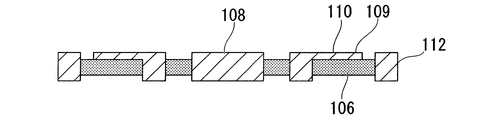
- the length of the wiring 110 on the semiconductor element electrode connection terminal 109 side becomes longer.
- This wiring is produced by half-etching a metal plate. The width and thickness of the wiring are small, and there is a problem that the yield is very poor due to the occurrence of bending or bending in the steps after the etching.
- FIG. 6C shows the state of the resin layer in the vicinity of the external connection terminal that has been heat-cured after printing. As schematically shown in FIGS. 6A to 6C, there is a concern that bubbles are formed beyond the external connection terminal in the printing direction (indicated by arrow D1).
- the present invention has been invented in view of such problems of the prior art, can cope well with an increase in the number of electrodes of a semiconductor element, does not contain bubbles, has high reliability, and is manufactured and has a semiconductor package. It is an object of the present invention to provide a lead frame substrate that can be stably assembled, a method for manufacturing the same, and a related semiconductor device.
- a metal plate having a first surface and a second surface, a semiconductor element mounting portion, a semiconductor element electrode connection terminal, and a first element formed on the first surface.
- the lead frame substrate is characterized in that at least one protrusion is formed on the side bottom of the first surface.
- a semiconductor element mounting portion, a semiconductor element electrode connection terminal, and an outer frame portion are formed on the first surface of the metal plate, and the semiconductor plate is formed on the second surface of the metal plate.
- a photoresist pattern for forming an external connection terminal connected to the device electrode connection terminal and an outer frame portion is formed, and the photoresist pattern for forming the external connection terminal has a protruding shape at one or more places.
- a hole not penetrating is formed in the exposed portion of the metal plate where the metal plate of the second surface is exposed by etching, and the direction of the protruding portion from the external connection terminal is formed in the hole.
- a liquid pre-mold resin is applied to the resin, a resin layer is formed by heat curing, and the first surface is etched to be electrically connected to the semiconductor element mounting portion and the external connection terminal.
- a manufacturing method of a lead frame substrate, and forming a semiconductor element electrode connecting terminal, and an outer frame portion is a manufacturing method of a lead frame substrate, and forming a semiconductor element electrode connecting terminal, and an outer frame portion.
- a metal plate having a first surface and a second surface, a semiconductor element mounting portion, a semiconductor element electrode connection terminal, and a first element formed on the first surface.
- a lead frame substrate having at least one projecting portion formed on a side bottom of the first surface; a semiconductor element mounted on the lead frame substrate; and the lead frame substrate and the semiconductor by wire bonding
- the electrical connection with the device is made,
- a semiconductor device comprising.
- external connection terminals for connecting to a printed wiring board can be arranged in an array on the entire back surface of the lead frame substrate, which can cope with an increase in the number of terminals of semiconductor elements. Moreover, since it is a board
- FIG. 3B is a cross-sectional view in the next step of FIG. 1B, illustrating an example of the method for manufacturing the lead frame substrate according to the embodiment of the present invention.
- FIG. 3A is a cross-sectional view in the next step of FIG. 1C, showing an example of the method for manufacturing the lead frame substrate of the embodiment of the present invention.
- FIG. 2C is a cross-sectional view in the next step of FIG. 1D, showing an example of the method for manufacturing the lead frame substrate of the embodiment of the present invention.
- FIG. 1B is a cross-sectional view in the next step of FIG. 1B, illustrating an example of the method for manufacturing the lead frame substrate according to the embodiment of the present invention.
- FIG. 3A is a cross-sectional view in the next step of FIG. 1C, showing an example of the method for manufacturing the lead frame substrate of the embodiment of the present invention.
- FIG. 2C is a cross-sectional view in the next step of FIG. 1D, showing an example of the method for manufacturing
- FIG. 8B is a cross-sectional view in the next step of FIG. 1E, illustrating an example of the method for manufacturing the lead frame substrate according to the embodiment of the present invention. It is a top view which shows the photoresist pattern in the lead frame board
- FIGS. 1A to 1F A schematic cross section of the manufacturing process of the lead frame substrate is shown in FIGS. 1A to 1F.
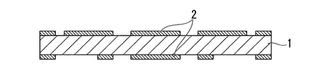
- Photoresist patterns 2 are formed on both surfaces of the metal plate 1 used for the lead frame (FIG. 1B). 1A to 1F, the pattern of the semiconductor element mounting portion 8, the connection terminal 9 to the semiconductor element electrode, the wiring 10, and the outer frame portion 12 is formed on the upper surface, and the pattern of the external connection terminal 11 and the outer frame portion is formed on the lower surface. To do.
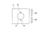
- one or more protrusions 13 are appropriately formed.
- the pattern of the protrusion 13 made of this photoresist is designed so that the second metal surface does not remain by subsequent etching.
- the pattern of the protrusions 13 is generally good to set the width to 30 ⁇ m or less and the length to 100 ⁇ m or less.
- the size of the protrusion 13 of the photoresist pattern is optimized by taking this into consideration. It is necessary to keep.
- the metal plate any material can be used as long as it has etching processability, mechanical strength, thermal conductivity, expansion coefficient, etc. as a lead frame, but an iron-nickel alloy represented by 42 alloy is used. In addition, a copper alloy to which various metal elements are added in order to improve mechanical strength is often used.
- Etching is performed from below using an etchant that dissolves the metal plate, such as ferric chloride, to form holes 3 (FIG. 1C). Since the remaining portion of the metal plate finally becomes a wiring, the depth of the hole 3 is preferably left about 10 to 50 ⁇ m thick so that a fine wiring can be formed at the time of etching from the second upper surface side.
- the external connection terminal is formed with at least one protrusion 14 as shown in FIGS. 2B and 2C.
- FIG. 2C shows a cross section between A2 and A2 in FIG. 2B, but the protrusion 14 is formed lower than the second surface.
- FIG. 2B shows a state in which the protruding portion 14 is formed at one place, and FIG.
- the liquid premold resin 5 is applied to the upper surface of the metal plate in the direction of arrow D5 (FIG. 1D).
- a printing technique for coating from the viewpoint of productivity and quality.
- any method can be used as long as it can be applied appropriately thickly, but screen printing is generally preferable.
- the direction of printing is performed in the directions of the arrow D2 in FIG. 2B and the arrows D3 and D4 in FIG. 2D, so that the flow of the pre-mold resin is given direction and bubbles can be prevented from being involved.
- the premold resin is cured by heating (FIG. 1E).
- the removal method can be selected from dry etching, mechanical polishing, chemical polishing, and the like. Further, the opposite surface was etched to form the semiconductor mounting portion 8, the semiconductor element electrode connection terminal 9, and the wiring 10 to obtain the lead frame substrate 7 (FIG. 1F). A top view of the external connection terminal side is shown in FIG.
- the external connection terminals can be arranged in an array, and it is possible to cope with the increase in the number of pins of the semiconductor element.
- FIG. 4A shows a cross-sectional view in which the semiconductor element 15 is mounted and wire-bonded.
- the semiconductor element 15 is pasted by the die attach material 17 and connected to the semiconductor element electrode connection terminal 9 by the gold wire 16.
- the semiconductor element electrode connection terminal is appropriately subjected to any of nickel-gold plating, tin plating, silver plating, nickel-palladium-gold plating, and the like.
- the lead frame substrate is placed on a heat block and bonded while being heated.
- the premold resin exists on the lower surface of the semiconductor element electrode connection terminal 9 and is hollow. Because the structure is difficult to assemble, it can be assembled without causing poor bonding.
- the semiconductor element side is sealed by transfer molding or potting, and the outer frame portion is separated with a diamond blade or the like to make small pieces (FIG. 4B).
- a semiconductor package using a lead frame substrate can be obtained by mounting solder balls on external connection terminals.
- a BGA (Ball Grid Array) type lead frame substrate will be described with reference to FIGS. 1A to 1F.
- the manufactured BGA has a 10 mm square package size and has a 168-pin array of external connection terminals on the lower surface of the package.
- a long strip-shaped copper alloy metal plate 1 (Furukawa Electric, EFTEC64T) having a width of 150 mm and a thickness of 200 ⁇ m was prepared.
- EFTEC64T Fluukawa Electric
- FIG. 1B on both surfaces of the metal plate 1, a photoresist (manufactured by Tokyo Ohka Kogyo Co., Ltd., OFPR4000) is coated with a roll coater to a thickness of 5 ⁇ m, and then pre-baked at 90 ° C. went.
- pattern exposure is performed from both sides through a photomask having a desired pattern, followed by development with a 1% aqueous sodium carbonate solution, followed by washing with water and post-baking to obtain a photoresist pattern 2 as shown in FIG. 1B. It was.
- a pattern for forming the semiconductor element mounting portion 8, the semiconductor element electrode connection terminal 9, the wiring 10, and the outer frame portion 12 is formed on the first surface, and the protrusion 13 is formed on the second surface.
- a pattern for forming the external connection terminal 11 and the outer frame portion 12 having (FIG. 2A) was formed.
- the shape of the protrusion 13 is an isosceles triangle having a width of 30 ⁇ m in contact with the external connection terminal and a length of 80 ⁇ m.
- a first etching process is performed from the second surface of the metal plate using a ferric chloride solution.
- the thickness of the metal plate portion exposed from the resist pattern on the second surface side was reduced to 30 ⁇ m (FIG. 1C).
- the protrusion part 14 about 40 micrometers in length was able to be formed in the external connection terminal side surface.
- the specific gravity of the ferric chloride solution used was 1.38, and the liquid temperature was 50 ° C.
- thermosetting resin SMC-376KF1, manufactured by Shin-Etsu Chemical Co., Ltd.
- the direction of printing was performed from the place where there was no protrusion 14 to the direction of the protrusion (FIG. 1D). Further, curing was performed at 180 ° C. for 3 hours to form a premold layer 13. The embedding property of the thermosetting resin was good, and no defects including bubbles were observed.
- thermosetting resin layer of about 1 ⁇ m remained on the surfaces of the external connection terminals 11 and the outer frame portion 12 that were not etched, an alkaline aqueous solution of potassium permanganate at 60 ° C. (40 g / L potassium permanganate + 20 g / L sodium hydroxide) was removed by treatment for about 3 minutes.
- a second etching process is performed from the first surface side of the metal plate with a ferric chloride solution to dissolve and remove the metal plate portion exposed from the resist pattern.
- the semiconductor element mounting portion 8, the semiconductor element electrode connection terminal 9, the wiring 10, and the outer frame portion 12 were formed (FIG. 1E).
- the external connection terminal 11 extends from the semiconductor element electrode connection terminal 9.
- the photoresist pattern 2 on the first surface was peeled off to obtain a desired lead frame type BGA substrate 7 (FIG. 1F).
- electrolytic nickel-gold plating was applied to the exposed metal surface.
- the thickness of nickel was 5 ⁇ m, and the thickness of gold was 0.1 ⁇ m (not shown).
- the semiconductor element 15 was mounted on the lead frame type BGA substrate 7 of the present invention using the die attach material 17, and the die attach material was cured at 150 ° C. for 1 hour. Furthermore, the wire of the semiconductor element electrode and the semiconductor element electrode connection terminal 9 were connected by wire bonding using a gold wire 16 having a diameter of 30 ⁇ m (FIG. 4A). When the wire bonding heating temperature was 200 ° C. and the pull strength of the wire on the semiconductor element electrode connection terminal side was measured, it was 9 g or more, and a good connection was obtained.
- the area including the semiconductor element and the semiconductor element electrode connection terminal was transfer-molded and cut into small pieces to obtain a semiconductor package using a lead frame type BGA substrate.
- a lead frame substrate of the present invention By using the method for manufacturing a lead frame substrate of the present invention, it becomes possible to obtain a lead frame substrate with reduced defects during manufacturing and semiconductor package assembly and improved reliability against thermal stress. It is applied to a multi-pin package substrate that cannot be handled by a type of semiconductor package.
Landscapes
- Engineering & Computer Science (AREA)
- Computer Hardware Design (AREA)
- Microelectronics & Electronic Packaging (AREA)
- Power Engineering (AREA)
- Physics & Mathematics (AREA)
- Condensed Matter Physics & Semiconductors (AREA)
- General Physics & Mathematics (AREA)
- Manufacturing & Machinery (AREA)
- Lead Frames For Integrated Circuits (AREA)
- Die Bonding (AREA)
Abstract
Description
本願は、2008年9月30日に、日本に出願された特願2008-254312に基づき優先権を主張し、その内容をここに援用する。
リードフレームは金属板の両面に所望のフォトレジストパターンを形成し、両面からエッチングすることにより、半導体素子搭載部、半導体素子電極との接続部であるインナーリード、アウターリード、これらを固定している外枠部を得ることができる。また、エッチング工法以外に、プレスによる打ち抜き加工によっても得ることができる。
半導体パッケージの組立工程としては、半導体素子搭載部に半導体素子をダイボンディングしたのち、金ワイヤー等を用いて、半導体素子の電極とインナーリードを電気的に接続する。その後、インナーリード部を含む半導体素子近傍を樹脂封止し、外枠部を断裁し、必要に応じてアウターリードに曲げ加工を施す。
そして近年、半導体素子の電極数が次第に増加するにつれて、アウターリードを側面に有するリードフレームタイプの半導体パッケージでは、もはや端子数が対応しきれなくなり、一部、BGA(Ball Grid Aray)やLGA(Land Grid Aray)タイプ等プリント配線基板との外部接続端子がパッケージ基板底面でアレイ状に配置された半導体パッケージへ置き換わってきている。
しかしながら、これらの基板の製造は工程が複雑になり、コスト高になるとともに、基板内の配線接続にめっきが使用されているため、リードフレームタイプのパッケージに比べ、信頼性が劣るという問題点がある。
BGAタイプのリードフレームでは、外部接続端子111の数が増加すると、半導体素子電極接続端子109側の配線110長が長くなる。この配線は金属板をハーフエッチングして作製するもので、その幅も厚さも小さく、エッチング以降の工程で折れや曲がりが発生して収率は非常に悪くなるという問題があった。
しかし、特許文献1の技術によると、本構造のリードフレーム基板に半導体素子を搭載し、ワイヤーボンディングにより半導体素子電極接続端子109を接続する際、接続端子109の下部は中空になっているため、ワイヤー接続の力が掛からず、接続不良が発生し、組み立て収率を著しく落とすという問題点があった。
このため、印刷技術を用いて第2の面に一定量プリモールド樹脂を塗布すると、比較的均一に樹脂層が形成される。外部接続端子上にも樹脂層が形成されるが、均一な膜厚のために除去工程が容易になると推察される。
図6Cは印刷後、熱硬化させた外部接続端子近傍の樹脂層の状態を示してる。図6A~図6Cに模式的に示すように、印刷方向(矢印D1で示す)に対して外部接続端子を越えた先に気泡が形成されてしまう問題点が心配される。
一方、本基板作製時において、配線の折れや曲がり、さらには気泡混入の不良が発生せず、半導体パッケージ組み立て工程であるワイヤーボンディング時において、ワイヤーボンディング接続端子の下部はプリモールド樹脂層が外部接続端子表面と面一に存在するため、安定して接続が可能となる。
リードフレームに用いられる金属板1の両面に、フォトレジストのパターン2を形成する(図1B)。図1A~図1Fでは上面に、半導体素子搭載部8、半導体素子電極との接続端子9、配線10、外枠部12のパターンを、下面に、外部接続端子11、外枠部のパターンを形成する。
このフォトレジストで出来た突起部13のパターンは、その後のエッチングで第2の金属面は残らないように設計する。
突起部13のパターンは、幅を30μm以下、長さを100μm以下に設定するのが一般に良い。但し、孔部3を形成するエッチング条件、エッチング量によって影響され、エッチング後に残った金属部分の大きさと形状が変化するので、それを考慮してフォトレジストパターンの突起部13のサイズを最適化しておく必要がある。
塩化第二鉄液等、金属板を溶解するエッチング液を用いて下面からエッチングを行い、孔部3を形成する(図1C)。孔部3の深さは金属板の残存部が最終的に配線になるため、第2回目の上面側からのエッチング時に微細配線が形成できるように10から50μm厚程度残すことが好ましい。
図2Cは、図2BのA2-A2間の断面を示すが、突出部14は第2の面よりも低く形成される。図2Bは突出部14が一箇所、図2Dは二箇所形成された状態を示す。
塗工は印刷技術を応用する事が、生産性や品質の面から一般に好ましい。印刷方法としては、適宜に厚く塗工できればどのような方法でも構わないが、一般にスクリーン印刷が好ましい。印刷の方向は、図2Bの矢印D2、図2Dの矢印D3、D4の方向に行うことにより、プリモールド樹脂の流れに方向性を持たせ、気泡の巻き込みを防止することができる。塗工後にプリモールド樹脂を加熱硬化させる(図1E)。
さらに、反対の面をエッチングして、半導体搭載部8、半導体素子電極接続端子9、配線10を形成してリードフレーム基板7を得た(図1F)。外部接続端子側の上面図を図3に示す。外部接続端子をアレイ状に配置することができ、半導体素子の多ピン化に対応が可能となった。
尚、ワイヤーボンディングを行う際、本リードフレーム基板をヒートブロックの上に載せ、加熱しながら接合を行うが、半導体素子電極接続端子9の下部にプリモールド樹脂が面一で存在し、また、中空構造が出来にくい為に、接合不良を起こさず組み立てることができる。
BGAタイプであればはんだボールを外部接続端子に搭載して、リードフレーム基板を用いた半導体パッケージが得られる。
製造したBGAのパッケージサイズは10mm角で、パッケージ下面には168ピンのアレイ状の外部接続端子を持つものである。
次いで、図1Bに示すように、この金属板1の両面に、ロールコーターでフォトレジスト(東京応化(株)製、OFPR4000)を5μmの厚さになるようにコーティングした後、90℃でプレベークを行った。
次に、所望のパターンを有するフオトマスクを介して両面からパターン露光し、その後1%炭酸ナトリウム水溶液で現像処理を行った後に水洗及びポストベークを行い、図1Bに示すようにフォトレジストパターン2を得た。
また、外部接続端子側面に、長さがおよそ40μmの突出部14を形成することができた。用いた塩化第二鉄溶液の比重は1.38、液温50℃であった。
さらに、180℃、3時間で硬化を行い、プリモールド層13を形成した。熱硬化樹脂の埋め込み性は良好で、気泡を含め不良は観察されなかった。
尚、図示していないが、下面側に不要なエッチングが行われないよう、第2回目のエッチング処理時には第2の面側にバックシート等を貼り付けておくのが好ましい。
次に、レジストの剥離後、露出した金属面に対し、電解ニッケル-金めっきを施した。
ニッケルの厚さは5μm、金の厚さは0.1μmであった(図示せず)。
ワイヤーボンディングの加熱温度は200℃で行い、半導体素子電極接続端子側のワイヤーのプル強度を測定したところ、9g以上あり、良好な接続が得られた。
2・・・フォトレジストパターン、
3・・・孔部、
4・・・スキージ、
5・・・液状プリモールド樹脂、
6・・・樹脂層、
7・・・リードフレーム基板、
8・・・半導体素子搭載部、
9・・・半導体素子電極接続端子、
10・・・配線、
11・・・外部接続端子、
12・・・外枠部、
13・・・フォトレジスト突起パターン、
14・・・突出部、
15・・・半導体素子、
16・・・金線、
17・・・ダイアタッチ材、
18・・・トランスファーモールド樹脂、
19・・・気泡
Claims (3)
- 第1の面と第2の面とを有する金属板と、
前記第1の面に形成された、半導体素子搭載部、半導体素子電極接続端子、および第1の外枠部と、
前記第2の面に形成され、前記半導体素子電極接続端子と電気的に接続された外部接続端子と、
前記第2の面に形成された第2の外枠部と、
前記第1の外枠部と前記第2の外枠部との間隙に形成された樹脂層と、を備えたリードフレーム基板であって、
前記樹脂層に埋設された前記外部接続端子の側面には、前記第1の面の側底部にかけて少なくとも1箇所の突出部が形成されていることを特徴とするリードフレーム基板。 - 金属板の第1の面に、半導体素子搭載部、半導体素子電極接続端子、および外枠部を形成し、
前記金属板の第2の面には、前記半導体素子電極接続端子と接続される外部接続端子、及び外枠部を、それぞれ形成する為のフォトレジストパターンを形成し、
前記外部接続端子の形成の為の前記フォトレジストパターンは一箇所以上の突起状のパターンを有するように形成し、
前記第2の面の金属板が露出した金属板露出部に、貫通しない孔部をエッチングにより形成し、
前記孔部に、前記外部接続端子から突出部の方向へ液状プリモールド樹脂を塗布したうえ、加熱硬化することにより樹脂層を形成し、
前記第1の面をエッチングすることにより、前記の半導体素子搭載部、前記外部接続端子と電気的に接続される前記半導体素子電極接続端子、及び外枠部を形成することを特徴とするリードフレーム基板の製造方法。 - 第1の面と第2の面とを有する金属板と、
前記第1の面に形成された、半導体素子搭載部、半導体素子電極接続端子、および第1の外枠部と、
前記第2の面に形成され、前記半導体素子電極接続端子と電気的に接続された外部接続端子と、
前記第2の面に形成された第2の外枠部と、
前記第1の外枠部と前記第2の外枠部との間隙に形成された樹脂層と、を備えたリードフレーム基板であって、
前記樹脂層に埋設された前記外部接続端子の側面には、前記第1の面の側底部にかけて少なくとも1箇所の突出部が形成されているリードフレーム基板と、
前記リードフレーム基板に、半導体素子が搭載され、且つ、ワイヤーボンディングで前記リードフレーム基板と前記半導体素子との電気的接続が成されていること、を特徴とする半導体装置。
Priority Applications (2)
| Application Number | Priority Date | Filing Date | Title |
|---|---|---|---|
| CN200980138144.0A CN102165585B (zh) | 2008-09-30 | 2009-09-30 | 引线框基板及其制造方法、半导体器件 |
| US13/064,205 US8558363B2 (en) | 2008-09-30 | 2011-03-10 | Lead frame substrate and method of manufacturing the same, and semiconductor device |
Applications Claiming Priority (2)
| Application Number | Priority Date | Filing Date | Title |
|---|---|---|---|
| JP2008254312A JP5549066B2 (ja) | 2008-09-30 | 2008-09-30 | リードフレーム型基板とその製造方法、及び半導体装置 |
| JP2008-254312 | 2008-09-30 |
Related Child Applications (1)
| Application Number | Title | Priority Date | Filing Date |
|---|---|---|---|
| US13/064,205 Continuation US8558363B2 (en) | 2008-09-30 | 2011-03-10 | Lead frame substrate and method of manufacturing the same, and semiconductor device |
Publications (1)
| Publication Number | Publication Date |
|---|---|
| WO2010038452A1 true WO2010038452A1 (ja) | 2010-04-08 |
Family
ID=42073232
Family Applications (1)
| Application Number | Title | Priority Date | Filing Date |
|---|---|---|---|
| PCT/JP2009/005041 WO2010038452A1 (ja) | 2008-09-30 | 2009-09-30 | リードフレーム基板とその製造方法、及び半導体装置 |
Country Status (6)
| Country | Link |
|---|---|
| US (1) | US8558363B2 (ja) |
| JP (1) | JP5549066B2 (ja) |
| KR (1) | KR101602982B1 (ja) |
| CN (1) | CN102165585B (ja) |
| TW (1) | TWI502711B (ja) |
| WO (1) | WO2010038452A1 (ja) |
Cited By (2)
| Publication number | Priority date | Publication date | Assignee | Title |
|---|---|---|---|---|
| CN102244060A (zh) * | 2011-06-02 | 2011-11-16 | 日月光半导体制造股份有限公司 | 封装基板及其制造方法 |
| US20120196407A1 (en) * | 2011-01-28 | 2012-08-02 | Shiann-Ming Liou | Single layer bga substrate process |
Families Citing this family (9)
| Publication number | Priority date | Publication date | Assignee | Title |
|---|---|---|---|---|
| TWI427716B (zh) * | 2010-06-04 | 2014-02-21 | 矽品精密工業股份有限公司 | 無載具之半導體封裝件及其製法 |
| US9142502B2 (en) * | 2011-08-31 | 2015-09-22 | Zhiwei Gong | Semiconductor device packaging having pre-encapsulation through via formation using drop-in signal conduits |
| US8916421B2 (en) * | 2011-08-31 | 2014-12-23 | Freescale Semiconductor, Inc. | Semiconductor device packaging having pre-encapsulation through via formation using lead frames with attached signal conduits |
| US8597983B2 (en) | 2011-11-18 | 2013-12-03 | Freescale Semiconductor, Inc. | Semiconductor device packaging having substrate with pre-encapsulation through via formation |
| JP2014072242A (ja) | 2012-09-27 | 2014-04-21 | Rohm Co Ltd | チップ部品およびその製造方法 |
| KR101505088B1 (ko) * | 2013-10-22 | 2015-03-23 | 앰코 테크놀로지 코리아 주식회사 | 반도체 패키지와 리드프레임 패들 구조 및 방법 |
| JP6266351B2 (ja) * | 2014-01-08 | 2018-01-24 | 新日本無線株式会社 | センサ装置およびその製造方法 |
| JP7182374B2 (ja) * | 2017-05-15 | 2022-12-02 | 新光電気工業株式会社 | リードフレーム及びその製造方法 |
| JP7039245B2 (ja) * | 2017-10-18 | 2022-03-22 | 新光電気工業株式会社 | リードフレーム及びその製造方法と電子部品装置 |
Citations (5)
| Publication number | Priority date | Publication date | Assignee | Title |
|---|---|---|---|---|
| JPH09307043A (ja) * | 1996-05-10 | 1997-11-28 | Dainippon Printing Co Ltd | リードフレーム部材とその製造方法、および該リードフレーム部材を用いた半導体装置 |
| JP2003309241A (ja) * | 2002-04-15 | 2003-10-31 | Dainippon Printing Co Ltd | リードフレーム部材とリードフレーム部材の製造方法、及び該リードフレーム部材を用いた半導体パッケージとその製造方法 |
| JP2003309242A (ja) * | 2002-04-15 | 2003-10-31 | Dainippon Printing Co Ltd | リードフレーム部材とリードフレーム部材の製造方法、及び該リードフレーム部材を用いた半導体パッケージとその製造方法 |
| JP2005117364A (ja) * | 2003-10-08 | 2005-04-28 | Murata Mfg Co Ltd | 弾性表面波装置の製造方法 |
| JP2005175261A (ja) * | 2003-12-12 | 2005-06-30 | Fujitsu Ten Ltd | 基板の電子部品実装構造および方法 |
Family Cites Families (15)
| Publication number | Priority date | Publication date | Assignee | Title |
|---|---|---|---|---|
| JP3642911B2 (ja) | 1997-02-05 | 2005-04-27 | 大日本印刷株式会社 | リードフレーム部材とその製造方法 |
| US6281568B1 (en) * | 1998-10-21 | 2001-08-28 | Amkor Technology, Inc. | Plastic integrated circuit device package and leadframe having partially undercut leads and die pad |
| JP3169919B2 (ja) * | 1998-12-21 | 2001-05-28 | 九州日本電気株式会社 | ボールグリッドアレイ型半導体装置及びその製造方法 |
| MY133357A (en) * | 1999-06-30 | 2007-11-30 | Hitachi Ltd | A semiconductor device and a method of manufacturing the same |
| KR100677651B1 (ko) * | 2001-04-13 | 2007-02-01 | 야마하 가부시키가이샤 | 반도체 소자 및 패키지와 그 제조방법 |
| TWI264099B (en) * | 2001-07-09 | 2006-10-11 | Sumitomo Metal Mining Co | Lead frame and manufacturing method therefor |
| KR100993277B1 (ko) * | 2002-04-30 | 2010-11-10 | 르네사스 일렉트로닉스 가부시키가이샤 | 반도체장치 및 전자 장치 |
| KR100993579B1 (ko) * | 2002-04-30 | 2010-11-10 | 르네사스 일렉트로닉스 가부시키가이샤 | 반도체장치 및 전자 장치 |
| JP2006520102A (ja) * | 2003-03-07 | 2006-08-31 | コーニンクレッカ フィリップス エレクトロニクス エヌ ヴィ | 半導体装置、半導体本体並びにその製造方法 |
| JP2004349316A (ja) * | 2003-05-20 | 2004-12-09 | Renesas Technology Corp | 半導体装置及びその製造方法 |
| JP2005191240A (ja) * | 2003-12-25 | 2005-07-14 | Renesas Technology Corp | 半導体装置及びその製造方法 |
| JP4417150B2 (ja) * | 2004-03-23 | 2010-02-17 | 株式会社ルネサステクノロジ | 半導体装置 |
| TWI262587B (en) * | 2005-03-08 | 2006-09-21 | Yi-Ling Jang | Leadframe and the manufacturing method thereof |
| US7687893B2 (en) * | 2006-12-27 | 2010-03-30 | Amkor Technology, Inc. | Semiconductor package having leadframe with exposed anchor pads |
| US8008784B2 (en) * | 2008-10-02 | 2011-08-30 | Advanced Semiconductor Engineering, Inc. | Package including a lead frame, a chip and a sealant |
-
2008
- 2008-09-30 JP JP2008254312A patent/JP5549066B2/ja not_active Expired - Fee Related
-
2009
- 2009-09-29 TW TW098132930A patent/TWI502711B/zh not_active IP Right Cessation
- 2009-09-30 CN CN200980138144.0A patent/CN102165585B/zh not_active Expired - Fee Related
- 2009-09-30 KR KR1020117006885A patent/KR101602982B1/ko not_active IP Right Cessation
- 2009-09-30 WO PCT/JP2009/005041 patent/WO2010038452A1/ja active Application Filing
-
2011
- 2011-03-10 US US13/064,205 patent/US8558363B2/en not_active Expired - Fee Related
Patent Citations (5)
| Publication number | Priority date | Publication date | Assignee | Title |
|---|---|---|---|---|
| JPH09307043A (ja) * | 1996-05-10 | 1997-11-28 | Dainippon Printing Co Ltd | リードフレーム部材とその製造方法、および該リードフレーム部材を用いた半導体装置 |
| JP2003309241A (ja) * | 2002-04-15 | 2003-10-31 | Dainippon Printing Co Ltd | リードフレーム部材とリードフレーム部材の製造方法、及び該リードフレーム部材を用いた半導体パッケージとその製造方法 |
| JP2003309242A (ja) * | 2002-04-15 | 2003-10-31 | Dainippon Printing Co Ltd | リードフレーム部材とリードフレーム部材の製造方法、及び該リードフレーム部材を用いた半導体パッケージとその製造方法 |
| JP2005117364A (ja) * | 2003-10-08 | 2005-04-28 | Murata Mfg Co Ltd | 弾性表面波装置の製造方法 |
| JP2005175261A (ja) * | 2003-12-12 | 2005-06-30 | Fujitsu Ten Ltd | 基板の電子部品実装構造および方法 |
Cited By (8)
| Publication number | Priority date | Publication date | Assignee | Title |
|---|---|---|---|---|
| US20120196407A1 (en) * | 2011-01-28 | 2012-08-02 | Shiann-Ming Liou | Single layer bga substrate process |
| WO2012103369A1 (en) * | 2011-01-28 | 2012-08-02 | Marvell World Trade Ltd. | Single layer bga substrate process |
| CN103339716A (zh) * | 2011-01-28 | 2013-10-02 | 马维尔国际贸易有限公司 | 单层bga基板工艺 |
| JP2014504032A (ja) * | 2011-01-28 | 2014-02-13 | マーベル ワールド トレード リミテッド | 単一層bga基板プロセス |
| US8673689B2 (en) | 2011-01-28 | 2014-03-18 | Marvell World Trade Ltd. | Single layer BGA substrate process |
| US8940585B2 (en) | 2011-01-28 | 2015-01-27 | Marvell World Trade Ltd. | Single layer BGA substrate process |
| TWI583267B (zh) * | 2011-01-28 | 2017-05-11 | 馬維爾國際貿易有限公司 | 單層球形柵格陣列基材製程方法 |
| CN102244060A (zh) * | 2011-06-02 | 2011-11-16 | 日月光半导体制造股份有限公司 | 封装基板及其制造方法 |
Also Published As
| Publication number | Publication date |
|---|---|
| TWI502711B (zh) | 2015-10-01 |
| KR101602982B1 (ko) | 2016-03-11 |
| JP2010087221A (ja) | 2010-04-15 |
| JP5549066B2 (ja) | 2014-07-16 |
| TW201021186A (en) | 2010-06-01 |
| US20110163435A1 (en) | 2011-07-07 |
| CN102165585A (zh) | 2011-08-24 |
| KR20110074514A (ko) | 2011-06-30 |
| US8558363B2 (en) | 2013-10-15 |
| CN102165585B (zh) | 2014-03-26 |
Similar Documents
| Publication | Publication Date | Title |
|---|---|---|
| JP5549066B2 (ja) | リードフレーム型基板とその製造方法、及び半導体装置 | |
| JP5532570B2 (ja) | リードフレーム型基板とその製造方法ならびに半導体装置 | |
| JP5407474B2 (ja) | 半導体素子基板の製造方法 | |
| JP5493323B2 (ja) | リードフレーム型基板の製造方法 | |
| TWI521661B (zh) | 導線架基板之製造方法與半導體裝置 | |
| JPH09246427A (ja) | 表面実装型半導体装置の製造方法および表面実装型半導体装置 | |
| JP2009147117A (ja) | リードフレーム型基板の製造方法及び半導体基板 | |
| JP5521301B2 (ja) | リードフレーム型基板とその製造方法および半導体装置 | |
| KR101148100B1 (ko) | 다열형 리드프레임 및 반도체 패키지의 제조방법 | |
| JPH10200009A (ja) | リードフレーム部材とリードフレーム部材の製造方法 |
Legal Events
| Date | Code | Title | Description |
|---|---|---|---|
| WWE | Wipo information: entry into national phase |
Ref document number: 200980138144.0 Country of ref document: CN |
|
| 121 | Ep: the epo has been informed by wipo that ep was designated in this application |
Ref document number: 09817493 Country of ref document: EP Kind code of ref document: A1 |
|
| ENP | Entry into the national phase |
Ref document number: 20117006885 Country of ref document: KR Kind code of ref document: A |
|
| NENP | Non-entry into the national phase |
Ref country code: DE |
|
| 122 | Ep: pct application non-entry in european phase |
Ref document number: 09817493 Country of ref document: EP Kind code of ref document: A1 |