WO2009139400A1 - Ultrasonic probe, method for manufacturing the same and ultrasonic diagnostic device - Google Patents
Ultrasonic probe, method for manufacturing the same and ultrasonic diagnostic device Download PDFInfo
- Publication number
- WO2009139400A1 WO2009139400A1 PCT/JP2009/058878 JP2009058878W WO2009139400A1 WO 2009139400 A1 WO2009139400 A1 WO 2009139400A1 JP 2009058878 W JP2009058878 W JP 2009058878W WO 2009139400 A1 WO2009139400 A1 WO 2009139400A1
- Authority
- WO
- WIPO (PCT)
- Prior art keywords
- cmut chip
- ultrasonic
- cmut
- ultrasonic probe
- conductive film
- Prior art date
Links
Images


Classifications
-
- B—PERFORMING OPERATIONS; TRANSPORTING
- B06—GENERATING OR TRANSMITTING MECHANICAL VIBRATIONS IN GENERAL
- B06B—METHODS OR APPARATUS FOR GENERATING OR TRANSMITTING MECHANICAL VIBRATIONS OF INFRASONIC, SONIC, OR ULTRASONIC FREQUENCY, e.g. FOR PERFORMING MECHANICAL WORK IN GENERAL
- B06B1/00—Methods or apparatus for generating mechanical vibrations of infrasonic, sonic, or ultrasonic frequency
- B06B1/02—Methods or apparatus for generating mechanical vibrations of infrasonic, sonic, or ultrasonic frequency making use of electrical energy
- B06B1/0292—Electrostatic transducers, e.g. electret-type
-
- A—HUMAN NECESSITIES
- A61—MEDICAL OR VETERINARY SCIENCE; HYGIENE
- A61B—DIAGNOSIS; SURGERY; IDENTIFICATION
- A61B8/00—Diagnosis using ultrasonic, sonic or infrasonic waves
- A61B8/44—Constructional features of the ultrasonic, sonic or infrasonic diagnostic device
- A61B8/4444—Constructional features of the ultrasonic, sonic or infrasonic diagnostic device related to the probe
- A61B8/4455—Features of the external shape of the probe, e.g. ergonomic aspects
-
- G—PHYSICS
- G01—MEASURING; TESTING
- G01N—INVESTIGATING OR ANALYSING MATERIALS BY DETERMINING THEIR CHEMICAL OR PHYSICAL PROPERTIES
- G01N29/00—Investigating or analysing materials by the use of ultrasonic, sonic or infrasonic waves; Visualisation of the interior of objects by transmitting ultrasonic or sonic waves through the object
- G01N29/22—Details, e.g. general constructional or apparatus details
- G01N29/24—Probes
- G01N29/2406—Electrostatic or capacitive probes, e.g. electret or cMUT-probes
-
- A—HUMAN NECESSITIES
- A61—MEDICAL OR VETERINARY SCIENCE; HYGIENE
- A61B—DIAGNOSIS; SURGERY; IDENTIFICATION
- A61B8/00—Diagnosis using ultrasonic, sonic or infrasonic waves
- A61B8/06—Measuring blood flow
-
- A—HUMAN NECESSITIES
- A61—MEDICAL OR VETERINARY SCIENCE; HYGIENE
- A61B—DIAGNOSIS; SURGERY; IDENTIFICATION
- A61B8/00—Diagnosis using ultrasonic, sonic or infrasonic waves
- A61B8/13—Tomography
-
- Y—GENERAL TAGGING OF NEW TECHNOLOGICAL DEVELOPMENTS; GENERAL TAGGING OF CROSS-SECTIONAL TECHNOLOGIES SPANNING OVER SEVERAL SECTIONS OF THE IPC; TECHNICAL SUBJECTS COVERED BY FORMER USPC CROSS-REFERENCE ART COLLECTIONS [XRACs] AND DIGESTS
- Y10—TECHNICAL SUBJECTS COVERED BY FORMER USPC
- Y10T—TECHNICAL SUBJECTS COVERED BY FORMER US CLASSIFICATION
- Y10T29/00—Metal working
- Y10T29/49—Method of mechanical manufacture
- Y10T29/49002—Electrical device making
- Y10T29/49005—Acoustic transducer
Definitions
- the present invention relates to an ultrasonic probe for imaging a diagnostic image, a manufacturing method thereof, and an ultrasonic diagnostic apparatus.
- the ultrasonic diagnostic apparatus is an apparatus that captures a diagnostic image based on a reflected echo signal output from an ultrasonic probe.
- a plurality of ultrasonic transducers are arranged on the ultrasonic probe.
- the ultrasonic transducer converts a drive signal into an ultrasonic wave and transmits the ultrasonic wave to the subject, and receives a reflected echo signal generated from the subject and converts it into an electrical signal.
- cMUT Capacitive Micromachined Ultrasonic Transducer
- cMUT is an ultrafine capacitive ultrasonic transducer manufactured by a semiconductor microfabrication process.
- the ultrasonic transmission / reception sensitivity that is, the electromechanical coupling coefficient changes according to the magnitude of the bias voltage.
- the bias voltage is applied so as to be superimposed on the drive signal supplied from the ultrasonic transmission / reception unit (see, for example, [Patent Document 1]).
- a DC voltage is applied as a bias voltage to the lower electrode with respect to the silicon substrate.
- an insulating layer is formed on the acoustic lens by vacuum evaporation, sputtering, CVD (Chemical Vapor Deposition), or the like.
- a conductive layer is formed on the cMUT chip. The insulating layer and the conductive layer are bonded with an adhesive.
- a cMUT probe having this structure when the cMUT probe is put on a disinfecting solution such as alcohol, the disinfecting solution becomes a solvent for the adhesive. The solvent dissolves the adhesive, and the dissolved adhesive penetrates the cMUT chip. The frame body and film body of the cMUT chip are cured by the penetrated adhesive. In the cMUT chip, the transmission and reception of ultrasonic waves by the internal space defined by the hardened frame body and film body become malfunctioning. Preventing the malfunction of cMUT chips based on such adhesive penetration has not been solved.
- An object of the present invention is to provide an ultrasonic probe, a method for manufacturing the ultrasonic probe, and an ultrasonic diagnostic apparatus that can prevent the malfunction of the cMUT chip based on the penetration of the adhesive.
- An ultrasonic probe includes a cMUT chip that has a plurality of vibration elements whose electromechanical coupling coefficient or sensitivity changes according to a bias voltage and transmits / receives ultrasonic waves, and an ultrasonic radiation side of the cMUT chip
- An ultrasonic probe comprising: the cMUT chip to which an insulating layer is bonded with an adhesive; and a housing portion for storing the acoustic lens, wherein the insulating layer includes at least one of silicon oxide or paraxylylene. And formed of a material that prevents permeation of the solvent of the adhesive into the adhesive portion.
- An ultrasonic probe manufacturing method includes a cMUT chip that has a plurality of vibration elements whose electromechanical coupling coefficients or sensitivities change according to a bias voltage, and transmits and receives ultrasonic waves.
- An acoustic lens provided on the acoustic wave emission side, a backing layer provided on the back side of the cMUT chip to absorb propagation of the ultrasonic wave, and provided on a side surface of the backing layer from a peripheral portion of the cMUT chip.
- An ultrasonic probe manufacturing method comprising: an electrical wiring portion in which a signal pattern connected to an electrode is disposed; and a housing portion that stores the cMUT chip, the acoustic lens, the backing layer, and the electrical wiring portion.
- the step of adhering the cMUT chip to the upper surface of the backing layer the step of adhering the electric wiring portion to the upper surface periphery of the backing layer, the electric wiring portion and the cMUT chip Connecting via a wire, filling the periphery of the wire with a photo-curing resin as a sealing material, forming a conductive film that can be connected to the ground on the ultrasonic radiation side of the cMUT chip, Adhering the acoustic lens to the ultrasonic radiation side of the cMUT chip.
- An ultrasound diagnostic apparatus includes an ultrasound probe that transmits and receives ultrasound to and from a subject, and image processing that configures an ultrasound image based on an ultrasound reception signal output from the ultrasound probe. And a display unit for displaying the ultrasonic image, wherein the ultrasonic probe is a first ultrasonic probe.
- the first ultrasonic probe includes a plurality of vibration elements whose electromechanical coupling coefficient or sensitivity changes according to a bias voltage, and a cMUT chip that transmits and receives ultrasonic waves, and an ultrasonic radiation side of the cMUT chip.
- An ultrasonic probe comprising: the cMUT chip to which the layer is bonded by an adhesive; and a housing portion for storing the acoustic lens, wherein the insulating layer includes at least one of silicon oxide or paraxylylene.
- the adhesive portion is formed of a material that prevents the solvent of the adhesive from penetrating into the adhesive portion.
- an ultrasonic probe it is possible to provide an ultrasonic probe, a manufacturing method thereof, and an ultrasonic diagnostic apparatus that can prevent the malfunction of the cMUT chip based on the penetration of the adhesive.
- Configuration diagram of ultrasonic diagnostic equipment 1 Configuration diagram of ultrasonic probe 2 Configuration diagram of vibrator 21 Configuration diagram of vibration element 28
- the figure which shows the manufacturing process of the ultrasound probe 2 shown in FIG. The figure which shows the ultrasonic probe 2f which concerns on 5th Embodiment Detailed view of electrical connection in Fig.
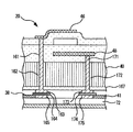
- FIG. 10 is a schematic sectional view showing an ultrasonic probe 2c according to a seventh embodiment.
- FIG. 10 is a top view of a cMUT wafer according to an eighth embodiment.
- FIG. 10 is a top view of a cMUT chip according to an eighth embodiment.
- FIG. 10 shows a method for forming a conductive film according to a ninth embodiment.
- FIG. 10 shows a method for forming a conductive film according to a tenth embodiment.
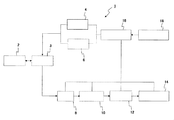
- FIG. 1 is a configuration diagram of the ultrasonic diagnostic apparatus 1.
- the ultrasonic diagnostic apparatus 1 includes an ultrasonic probe 2, a transmission / reception separation unit 3, a transmission unit 4, a bias unit 6, a reception unit 8, a phasing addition unit 10, an image processing unit 12, a display unit 14, a control unit 16, The operation unit 18 is configured.
- the ultrasonic probe 2 is a device that transmits and receives ultrasonic waves to and from the subject by contacting the subject. Ultrasonic waves are transmitted from the ultrasonic probe 2 to the subject, and reflected echo signals from the subject are received by the ultrasonic probe 2.
- the transmission unit 4 and the bias unit 6 are devices that supply drive signals to the ultrasonic probe 2.
- the receiving unit 8 is a device that receives a reflected echo signal output from the ultrasound probe 2.
- the receiving unit 8 further performs processing such as analog-digital conversion on the received reflected echo signal.
- the transmission / reception separating unit 3 switches between transmission and reception so as to pass a drive signal from the transmission unit 4 to the ultrasonic probe 2 at the time of transmission, and to pass a reception signal from the ultrasonic probe 2 to the reception unit 8 at the time of reception. To do.
- the phasing adder 10 is a device for phasing and adding the received reflected echo signals.
- the image processing unit 12 is a device that constructs a diagnostic image (for example, a tomographic image or a blood flow image) based on the reflected echo signal subjected to phasing addition.
- a diagnostic image for example, a tomographic image or a blood flow image
- the display unit 18 is a display device that displays a diagnostic image subjected to image processing.
- the control unit 16 is a device that controls each component described above.
- the operation unit 18 is a device that gives an instruction to the control unit 16.
- the operation unit 18 is an input device such as a trackball, a keyboard, or a mouse.
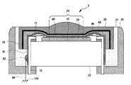
- FIG. 2 is a configuration diagram of the ultrasound probe 2.
- FIG. 2 is a partially cutaway perspective view of the ultrasound probe 2.
- the ultrasonic probe 2 includes a cMUT chip 20.
- the cMUT chip 20 is a one-dimensional array type vibrator group in which a plurality of vibrators 21-1, vibrators 21-2,. A plurality of vibration elements 28 are disposed on the vibrator 21-1, the vibrator 21-2,. Note that another form of transducer group such as a two-dimensional array type or a convex type may be used.
- a backing layer 22 is provided on the back side of the cMUT chip 20.
- An acoustic lens 26 is provided on the ultrasonic emission side of the cMUT chip 20.
- the cMUT chip 20, the backing layer 22, and the like are stored in the ultrasonic probe cover 25.
- the cMUT chip 20 converts the drive signals from the transmission unit 4 and the bias unit 6 into ultrasonic waves and transmits the ultrasonic waves to the subject.
- the receiving unit 8 converts ultrasonic waves generated from the subject into electric signals and receives them as reflected echo signals.
- the backing layer 22 is a layer that suppresses the propagation of ultrasonic waves emitted from the cMUT chip 20 to the back side and suppresses excessive vibration.
- the acoustic lens 26 is a lens that converges the ultrasonic beam transmitted from the cMUT chip 20.
- the curvature of the acoustic lens 26 is determined based on one focal length.
- a matching layer may be provided between the acoustic lens 26 and the cMUT chip 20.
- the matching layer is a layer that improves the transmission efficiency of ultrasonic waves by matching the acoustic impedances of the cMUT chip 20 and the subject.
- FIG. 3 is a configuration diagram of the vibrator 21.
- the upper electrode 46 of the vibration element 28 is connected to each vibrator 21 divided in the long axis direction X. That is, the upper electrode 46-1, the upper electrode 46-2, ... are arranged in parallel in the major axis direction X.
- the lower electrode 48 of the vibration element 28 is connected for each section divided in the short axis direction Y. That is, the lower electrode 48-1, the lower electrode 48-2,... Are arranged in parallel in the minor axis direction Y.
- FIG. 4 is a configuration diagram of the vibration element 28.
- FIG. 4 is a cross-sectional view of one vibration element 28.
- the vibration element 28 includes a substrate 40, a film body 44, a film body 45, an upper electrode 46, a frame body 47, and a lower electrode 48.
- the vibration element 28 is formed by fine processing by a semiconductor process.
- the vibration element 28 corresponds to one element of the cMUT.
- the substrate 40 is a semiconductor substrate such as silicon.
- the film body 44 and the frame body 47 are formed from a semiconductor compound such as a silicon compound.
- the film body 44 is provided on the ultrasonic wave emission side of the frame body 47.
- An upper electrode 46 is provided between the film body 44 and the frame body 47.
- a lower electrode 48 is provided on the film body 45 formed on the substrate 40.
- the internal space 50 defined by the frame body 47 and the film body 45 is in a vacuum state or filled with a predetermined gas.
- the upper electrode 46 and the lower electrode 48 are connected to a transmission unit 4 that supplies an AC high frequency voltage as a drive signal and a bias unit 6 that applies a DC voltage as a bias voltage, respectively.
- a DC bias voltage (Va) is applied to the vibration element 28 via the upper electrode 46 and the lower electrode 48, and an electric field is generated by the bias voltage (Va).
- the film body 44 is strained by the electric field generated and becomes a predetermined electromechanical coupling coefficient (Sa).
- a drive signal is supplied from the transmitter 4 to the upper electrode 46, ultrasonic waves are emitted from the film body 44 based on the electromechanical coupling coefficient (Sa).
- the film body 44 when receiving an ultrasonic wave, the film body 44 is excited by a reflected echo signal generated from the subject, and the capacity of the internal space 50 changes. Based on the amount of change in the internal space 50, an electrical signal is detected via the upper electrode 46.
- the electromechanical coupling coefficient of the vibration element 28 is determined by the degree of tension of the film body 44. Therefore, if the tension of the film body 44 is controlled by changing the magnitude of the bias voltage applied to the vibration element 28, even if a drive signal having the same amplitude is input, the supersonic wave emitted from the vibration element 28 is exceeded.
- the sound pressure (for example, amplitude) of the sound wave can be changed.
- FIG. 5 is a diagram showing the ultrasonic probe 2 according to the first embodiment.
- FIG. 5 is a plane A sectional view of the ultrasonic probe 2 of FIG.
- the conductive film 76 is formed along the ultrasonic radiation surface of the cMUT chip 20, the side surfaces of the flexible substrate 72 and the backing layer 22, and the insulating film 78 which is an insulating layer is formed on the inner surface of the acoustic lens 26.
- the conductive film 76 and the insulating film 78 are formed by, for example, vacuum deposition, sputtering, or CVD, and the conductive film 76 is a Cu or AI film or the like and has electrical conductivity.
- the insulating film 78 is bonded to the conductive film 76 with an adhesive.
- the insulating film 78 is, for example, a silicon oxide film, a paraxylylene film, etc., and has chemical resistance.
- the chemical resistance is to suppress, for example, penetration of the cMUT chip 20 by an adhesive that adheres to the acoustic lens 26.
- the conductive film 76 is connected to the ground 120 on the main device side via a connection part 82 and a ground line 84 by soldering, conductive adhesive, or the like.
- the electrical safety of the ultrasonic probe 2 with respect to the subject can be improved.
- an insulating film 78 is formed as an insulating layer between the acoustic lens 26 and the cMUT chip 20, and the subject and the cMUT chip 20 are double-insulated by the acoustic lens 26 and the insulating layer 78. Therefore, the safety of the ultrasonic probe 2 is improved. Note that the electrical safety can be further improved by providing two or more insulating layers rather than the single insulating layer 78.
- the conductive film 76 is formed on the ultrasonic radiation surface of the cMUT chip 20, it is not necessary to form a conductive film on the inner surface of the acoustic lens 26. Further, since the conductive film 76 is formed along the side surfaces of the flexible substrate 72 and the backing layer 22, it is possible to directly connect the conductive film 76 and the ground line 84 via the connection portion 82 with the backing layer 22 as a base. it can.
- the cMUT chip 20 is bonded to the upper surface of the backing layer 22 through the adhesive layer 70.
- a flexible substrate 72 Flexible Printed Circuits: FPC
- FPC Flexible Printed Circuits
- the adhesive layer 70 and the adhesive layer 71 are, for example, an adhesive made of an epoxy resin.
- the height of the cMUT chip 20 and the flexible substrate 72 can be adjusted by arbitrarily adjusting the layer thicknesses of the adhesive layer 70 and the adhesive layer 71.
- the flexible substrate 72 and the cMUT chip 20 are electrically connected via a wire 86.
- the wire 86 is connected by a wire bonding method.
- an Au wire or the like can be used.
- a photo-curing resin 88 is filled around the wire 86 as a sealing material.
- the sealing material may be a thermosetting resin.
- the thermosetting resin is made of a material having the same thermal expansion coefficient as that of the semiconductor base material. However, the thermosetting resin can improve the material strength due to thermal expansion as compared with the photo-curing resin.
- a flip chip bonding method in which pads are connected may be used. If the flip chip bonding method is used, the mounting restrictions such as the chip size can be relaxed rather than the internal connection by the wire bonding method.
- the acoustic lens 26 is bonded to the cMUT chip 20 via the adhesive layer 90 between the insulating film 78 formed on the inner surface and the conductive film 76 formed on the ultrasonic radiation surface of the cMUT chip 20.
- a material of the acoustic lens 26 for example, silicon rubber is used.
- the material of the adhesive layer 90 it is desirable to use a material similar to the acoustic lens 26 (for example, silicon resin).
- the ultrasonic radiation surface of the acoustic lens 26 is convex in the ultrasonic irradiation direction at least within the region 23.
- the vibration element 28 is disposed at least in a range corresponding to the region 23. Ultrasonic waves are irradiated from the convex portion of the acoustic lens 26.
- the back surface of the acoustic lens 26 has a recess at a position corresponding to the periphery of the cMUT chip 20. In this recess, a connection portion (a portion of the photo-curing resin 88) between the cMUT chip 20 and the flexible substrate 72 is fitted.
- the ultrasonic probe cover 25 is provided on the four sides of the ultrasonic probe 2.
- the ultrasonic probe cover 25 is fixed to the four side surfaces of the acoustic lens 26.
- the examiner operates the ultrasonic probe 2 by holding the ultrasonic probe cover 25 by hand.
- a sealing material 27 is filled in the gap between the ultrasonic probe cover 25 and the acoustic lens 26.
- the upper end position of the ultrasound probe cover 25 is preferably located above the cMUT chip 20. As a result, even if an unexpected situation such as a drop of the ultrasound probe 2 occurs, it is possible to protect the cMUT chip 20 by preventing a direct impact.
- FIG. 6 is a schematic diagram showing the connection between the ultrasonic diagnostic apparatus 1 and the ultrasonic probe 2. As shown in FIG. The ultrasonic diagnostic apparatus 1 and the ultrasonic probe 2 are connected via a cable 82.
- the cable 82 has a plurality of coaxial cables 96.
- the upper electrode 46 of the vibration element 28 is connected to the wiring 85.
- the wiring 85 is connected to the wiring 91 in the ultrasonic diagnostic apparatus 1 via the inner conductor of the coaxial cable 96.
- the wiring 91 is connected to the reception amplifier 100 and the transmission unit 4 in the reception unit 8 via the transmission / reception separation circuit 98.
- the lower electrode 48 of the vibration element 28 is connected to the wiring 66.
- the wiring 66 is connected to the wiring 62 in the ultrasonic diagnostic apparatus 1 via the inner conductor of the coaxial cable 96.
- the wiring 62 is connected to the bias unit 6.
- the number of the coaxial cables 96 is the total number of the upper electrode 46 and the lower electrode 48 that are commonly disposed in the plurality of vibration elements 28.
- the substrate 40 of the vibration element 28 is connected to the wiring 87.
- the wiring 87 is connected to the wiring 93 in the ultrasonic diagnostic apparatus 1 via the outer conductor of the coaxial cable 96.
- the wiring 93 is connected to the ground 108 via the chassis ground of the main unit (not shown).
- a capacitor 112 is disposed between the wiring 66 and the wiring 87.
- the capacitor 112 is a capacitive element for bypassing a signal current for bypassing the current from the lower electrode 48 when an AC current flows from the upper electrode 46 to the lower electrode 48.
- a resistor 110 is disposed between the wiring 91 and the wiring 93.
- the resistor 110 is a resistance element for stabilizing the DC potential of the upper electrode 46 to the ground potential.
- the bias unit 6 is disposed between the wiring 62 and the wiring 93.
- the bias unit 6 generates a potential difference between the upper electrode 46 and the lower electrode 48.
- the transmission unit 4 applies an AC high frequency voltage to the upper electrode 46 as a drive signal.
- the conductive film 76 of the vibration element 28 is connected to the wiring 84.
- the wiring 84 is formed so as to cover the internal circuit (the wiring 85, the wiring 66, the capacitor 112, etc.) of the ultrasonic probe 2, and the wiring 99 in the ultrasonic diagnostic apparatus 1 is connected via the outer periphery of the cable 82. It is connected to the.
- the conductive film 76, the wiring 84, the outer periphery of the cable 82, the wiring 99 and the ground 120 form a protection circuit so that electromagnetic waves from the outside do not enter the internal circuits of the ultrasonic diagnostic apparatus 1 and the ultrasonic probe 2. In addition, the electricity generated inside the ultrasonic diagnostic apparatus 1 and the ultrasonic probe 2 is prevented from being emitted to the outside.
- the insulating layer 78 is provided on the ultrasonic radiation side of the cMUT chip 20. Therefore, malfunction of the cMUT chip based on the penetration of the adhesive can be prevented.
- the conductive film 76 is disposed on the ultrasonic radiation surface side of the cMUT chip 20, even when the radiation-side acoustic lens 26 is damaged, the conductive film 76 prevents electric shock because of the ground potential, and the ultrasonic probe for the subject is detected. The electrical safety of the touch element can be improved.
- a closed space having a ground potential is formed by the conductive film 76, the ground line 84, and the chassis ground of the main unit.
- the conductive film 76 is formed along the inner surface and the outer surface of the acoustic lens 26, and is grounded through the highly reliable conductive member 80 and the ground wire 84. Connected to 120.
- the conductive film 76 formed along the inner and outer surfaces of the acoustic lens 26 is connected to the ground wire 84 easily and reliably through the conductive member 80 instead of the sheet-like conductive film drawn out by in-mold molding. be able to. Mounting reliability and workability can be improved.
- the highly reliable conductive member 80 it is possible to prevent the conductive member 80 from being damaged when fixed to the flexible substrate 72.
- the conductive member 80 and the ground wire 84 are illustrated only on the left side surface of the flexible substrate 72 in the drawing, but may be provided on at least one of the four side surfaces of the flexible substrate 72.
- FIG. 7 is a diagram showing an ultrasonic probe 2a according to the second embodiment.
- FIG. 7 corresponds to a cross-sectional view taken along the plane A in FIG.
- the conductive film 76 is formed along the ultrasonic radiation surface of the cMUT chip 20, the side surfaces of the flexible substrate 72 and the backing layer 22, and is connected to the ground line 84 via the bonding portion 82.
- an insulating film 78a which is an insulating layer, is formed between the cMUT chip 20 and the conductive film 76.
- the insulating film 78 which is an insulating layer, is formed on the inner surface of the acoustic lens 26, as in the first embodiment.
- the second embodiment similarly to the first embodiment, it is possible to prevent malfunction of the cMUT chip based on the penetration of the adhesive.
- the conductive film 76 as a ground layer is provided on the ultrasonic radiation side of the cMUT chip 20, the electrical safety of the ultrasonic probe 2a with respect to the subject can be improved, and the insulating film 78a is provided. As a result, the electric withstand voltage between the conductive film 76 and the wire 86 and between the conductive film 76 and the cMUT chip 20 can be improved.
- FIG. 8 is a schematic diagram showing the wiring of the ultrasonic probe 2.
- FIG. 9 is a diagram showing the ground connection of the substrate 40 of the cMUT chip 20, and is a cross-sectional view taken along the line BB ′ of FIG.
- the upper electrode 46 of the MUT chip 20 and the signal pattern 38 of the flexible board 72 are connected by a wire 86-1, and the lower electrode 48 of the MUT chip 20 and the signal pattern 41 of the flexible board 72 are connected. Connected with wire 86-2.
- a photo-curing resin 88 is filled around the wire 86 to seal the connection.
- a conductive resin 89 is filled between the cMUT chip 20 and the flexible substrate 72.
- the conductive resin 89 corresponds to a connection portion between the substrate 40 of the cMUT chip 20 and the ground line 94.
- the ground line 94 is disposed between the flexible substrate 72 and the backing layer 22 at the corner of the cMUT chip 20.
- the substrate 40 is provided on the bottom surface of the cMUT chip 20.
- the substrate 40 is electrically connected to the conductive resin 89.
- the substrate 40 is connected to the ground 108 via the conductive resin 89 and the ground line 94.
- the ground line 94 in FIG. 9 corresponds to the wiring 87 in FIG.
- the conductive resin 89 is provided at a connection portion between the substrate 40 and the wiring 87.
- the signal pattern 38 of the flexible substrate 72 and the wire 86 for connecting the signal pattern 41 and the cMUT chip 20 exist on the peripheral edge other than the corner of the cMUT chip 20, but the substrate 40 and the ground line 94 of the cMUT chip 20 exist. Are connected via a conductive resin 89 filled in the corners of the cMUT chip 20.
- the signal pattern connection portion and the substrate ground connection portion can be independently provided at different locations, and the manufacture is also easy.
- the substrate 40 itself is also a semiconductor, the substrate 40 may become a high voltage when an abnormality occurs.
- the substrate 40 by connecting the substrate 40 to the ground, the substrate 40 can be maintained at the ground potential even when an abnormality occurs, and the safety of the ultrasonic probe 2 can be ensured.
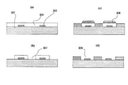
- FIG. 10 is a diagram showing a manufacturing process of the ultrasonic probe 2 shown in FIG.
- the cMUT chip 20 is adhered to the upper surface of the backing layer 22 by the adhesive layer 70 (step S1).
- the flexible substrate 72 is bonded to the periphery of the upper surface of the backing layer 22 by the adhesive layer 71 (step S2).
- the flexible substrate 72 and the cMUT chip 20 are electrically connected via the wire 86.
- the wire 86 is connected by a wire bonding method or a flip chip bonding method (step S3).
- a photo-curing resin 88 is filled around the wire 86 as a sealing material (step S4).
- a conductive film 76 is formed (step S5).
- the acoustic lens 26 is formed (step S6), and the insulating film 78 is formed on the inner surface of the acoustic lens 26 (step S7).
- the acoustic lens 26 is bonded to the ultrasonic radiation surface of the cMUT chip 20 by the adhesive layer 90.
- the conductive film 76 is connected to the ground line 84.
- An ultrasonic probe cover 25 is attached.
- a sealing material 27 is filled in a gap between the acoustic lens 26 or the flexible substrate 72 and the ultrasonic probe cover 25 (step S8).
- the ultrasonic probe 2 shown in FIG. 5 is manufactured.
- the insulating film 78a may be formed before the conductive film 76 is formed. In this case, the ultrasonic probe 2a shown in FIG. 7 is manufactured.
- the film forming method there are a method of in-mold molding of an insulating sheet with a conductive film simultaneously with the molding of the acoustic lens 26, and a method of forming an insulating film or a conductive film by physical vapor deposition or chemical vapor deposition.
- In-mold molding can form a film at low cost, but a film thickness of about 10 ⁇ m is the limit.
- the film thickness can be about 1 ⁇ m.
- the fifth embodiment relates to electrical connection between the cMUT chip 20 and the flexible substrate 72.
- FIG. 11 is a diagram showing an ultrasonic probe 2f according to the fifth embodiment.
- FIG. 11 corresponds to a cross-sectional view taken along the plane A in FIG.
- FIG. 12 is a detailed view of the electrical connection portion of FIG.
- the flexible substrate 72 and the cMUT chip 20 are described as being electrically connected via the wire 86 by the wire bonding method, but in the fifth embodiment, the through-hole 161 or the through-hole 161 is used.
- the flexible substrate 72 and the cMUT chip 20 are electrically connected through the hole 171.
- the signal pattern of the flexible substrate 72 is electrically connected to the electrode of the cMUT chip 20 on the back surface of the peripheral edge of the cMUT chip 20.
- a notch 168 is provided on the upper surface of the peripheral portion of the backing layer 22 in accordance with the thickness of the flexible substrate 72, the adhesive layer 71, and the adhesive layer 70.
- the through hole 161 is a conduction path between the upper electrode 46 of the cMUT chip 20 and the pad terminal 163 provided on the back surface of the cMUT chip 20.
- the through hole 171 is a conduction path between the lower electrode 48 of the cMUT chip 20 and the pad terminal 173 provided on the back surface of the cMUT chip 20.
- the through hole 161 and the through hole 171 are filled with metal or a metal layer is formed on the inner wall surface.
- an insulating portion 162 and an insulating portion 172 are provided around the through hole 161 and the through hole 171. It is desirable to provide the insulating layer 167 also on the back surface of the substrate 40.
- the pad terminal 165 and the pad terminal 175 provided on the flexible substrate 72 are respectively connected to the pad terminal 163 and the pad terminal 173 provided on the lower surface of the cMUT chip 20 by a conductive adhesive 164 and a conductive adhesive 174 such as an anisotropic conductive adhesive sheet. Is electrically connected.
- the signal pattern 38 of the flexible substrate 72 is electrically connected to the upper electrode 46 of the cMUT chip 20 through the pad terminal 165, the conductive adhesive 164, the pad terminal 163, and the through hole 161.
- the signal pattern 41 of the flexible substrate 72 is electrically connected to the lower electrode 48 of the cMUT chip 20 through the pad terminal 175, the conductive adhesive 174, the pad terminal 173, and the through hole 171.
- the flexible substrate 72 and the cMUT chip 20 are electrically connected through the through hole 161 and the through hole 171.
- the electrical connection between the flexible substrate 72 and the cMUT chip 20 can be performed only by aligning the pad terminals without requiring a wire for electrical connection.
- the electrical connection is made through the through hole on the back surface of the cMUT chip 20, but the electrical connection may be made through the through hole on the ultrasonic radiation surface of the cMUT chip 20.
- the high potential wire 86 and the ground potential conductive film 76 are close to each other.
- the ground potential of the conductive film 76 cannot be maintained due to a short circuit between the conductive film 78 and the wire 86 due to a defective sealing material such as the cured resin 88 or a pinhole defect of the insulating film 78.
- the connection line and the conductive film 76 are not close to each other, so there is no possibility of short-circuiting. Since the ground potential of the film 76 is maintained, safety is ensured.
- the wire 86 used in the wire bonding method shown in FIG. 5 or the like is a thin metal wire, it is easily damaged by an action force and difficult to handle.
- wire connection work by the wire bonding method is unnecessary, and handling is easy.
- a sealing material such as a photo-curing resin 88 is required to fill the periphery of the wire 86.
- the linear expansion coefficient is different between the resin used as the sealing material and the wire 86.
- the linear expansion coefficient of resin used as a sealing material is larger than that of metal. For this reason, if the resin used as the sealing material expands due to a temperature change, the wire 86 may be damaged.
- impurities exist in the resin used as the sealing material, there is a possibility that the wire 86 and the conductive film 76 are short-circuited due to electrical migration.
- a wire and a sealing material are not required, and therefore no problem due to impurities in the resin occurs.
- the safety of the ultrasonic probe 2 can be further improved by performing the connection by the through hole instead of the connection by the wire bonding method.
- the sixth embodiment relates to ground connection of the substrate 40 of the cMUT chip 20.
- the substrate 40 is described as being connected to the ground from the side surface of the cMUT chip 20 via the conductive resin 89.
- the upper surface side (ultrasonic radiation) of the cMUT chip 20 is described.
- the substrate 40 is grounded from the surface side) or the lower surface side (back side).
- FIG. 13 is a diagram showing the ground connection of the substrate 40 from the upper surface side of the cMUT chip 20.
- the through hole 181 is a conduction path between the substrate 40 of the cMUT chip 20 and the pad terminal 182 provided on the upper surface of the cMUT chip 20.
- the through hole 185 is a conduction path between the ground line 94 provided on the inner surface of the flexible substrate 72 and the pad terminal 184 provided on the upper surface.
- the through hole 181 and the through hole 185 are filled with metal, or a metal layer is formed on the inner wall surface.
- the pad terminal 182 and the pad terminal 184 are electrically connected via the wire 183 by a wire bonding method.
- the substrate 40 of the cMUT chip 20 is connected to the ground 108 through the through hole 181, the pad terminal 182, the wire 183, the pad terminal 184, the through hole 185, and the ground line 94.
- FIG. 14 is a diagram showing the ground connection of the substrate 40 from the lower surface side of the cMUT chip 20.
- the through hole 191 is a conduction path between the substrate 40 of the cMUT chip 20 and the pad terminal 192 provided on the lower surface of the cMUT chip 20.
- the through hole 195 is a conduction path between the ground line 94 provided on the inner surface of the flexible substrate 72 and the pad terminal 194 provided on the upper surface.
- the through hole 191 and the through hole 195 are filled with metal, or a metal layer is formed on the inner wall surface.
- the pad terminal 192 and the pad terminal 194 are electrically connected by a conductive adhesive 193 such as an anisotropic conductive adhesive sheet.
- the substrate 40 of the cMUT chip 20 is grounded through a through hole 191, a pad terminal 192, a conductive adhesive 193, a pad terminal 194, a through hole 195, and a ground line 94.
- the substrate 40 of the cMUT chip 20 can be grounded from the upper surface side or the lower surface side of the cMUT chip 20 through the through hole.
- the ground connection of the substrate 40 of the cMUT chip 20 can be performed only by performing the connection by the wire bonding method and the alignment of the pad terminals.
- An upper electrode 46 and a lower electrode 48 to which a high voltage of 100 V or higher is applied exist on the substrate 40 of the cMUT chip chip 20. Since the substrate 40 itself is also a semiconductor, the substrate 40 may become a high voltage when an abnormality occurs. In the sixth embodiment, by connecting the substrate 40 to the ground via the through hole, the substrate 40 can be maintained at the ground potential even when an abnormality occurs, and the safety of the ultrasonic probe 2 is ensured. be able to.
- a conductive film 201 is formed on the cMUT chip 20, and the conductive film 201 is formed by a process of manufacturing a cMUT wafer before dividing a large number of cMUT chips. Since the cMUT wafer is manufactured using a semiconductor process, the conductive film 201 is formed in a wafer state.
- the conductive film in the above semiconductor process AI, AICu alloy, or Cu is used, but any conductive material such as Ti, Cr, Au, Pt, TiN, TiW, Si3N4 can be applied.
- the conductive film 201 can be formed after the cMUT wafer manufacturing process is completed. However, in order to prevent foreign matter from remaining, the conductive film 201 is formed in a wafer state before the cMUT wafer is divided by dicing or the like. Is preferred. In this case, the conductive coating material can also be formed by spin coating or spray coating.
- a conductive film 203 is formed on the flexible substrate 204, which is formed when the flexible substrate 204 is manufactured.
- the conductive film 203 can be formed by attaching a metal coat or Cu tape after the flexible substrate 204 is formed.
- the conductive film 201 of the cMUT chip 20 and the conductive film 203 of the flexible substrate 204 are electrically connected by a conductive film 202.
- the conductive film 202 is formed using a conductive tape such as a Cu tape or an AI tape, or a conductive paste kneaded with Ag particles or C particles.
- the cMUT chip 20 and the flexible substrate 204 are mounted, and in the conductive film of foreign matter during the mounting process such as the wire bonding process and the photocuring resin filling process. Therefore, there is no influence on the vibration element due to pressurization in the acoustic lens bonding process, and a stable probe can be formed.
- FIG. 16 is a diagram in which a plurality of cMUT chips 302 are laid out in the plane of the cMUT wafer 301.
- the cMUT wafer 301 is manufactured using, for example, an 8 inch, 6 inch, or 12 inch wafer.
- dicing is performed along the scribe line 310 to separate each cMUT chip 302.
- FIG. 17 is an enlarged schematic diagram of one cMUT chip 302.
- the cMUT chip 302 is formed with an electrode pad 303 for electrical connection with the outside.
- FIG. 18 is a view as seen from the DD cross section of FIG.
- a conductive film 202 is formed by CVD or sputtering on a cMUT wafer 301 on which a vibration element (not shown) is completed (a).
- a photoresist 304 is formed by a spin coater or spray (b).
- a photoresist opening 305 is formed in the photoresist 304 by photolithography (c).
- a conductive film opening 306 of an electrode pad is formed in the conductive film 202 by dry etching or wet etching (d). Finally, the photoresist 304 is removed and washed to complete the formation of the conductive film 202 and the formation of the conductive film opening 306 of the electrode pad 303 for external conduction by wire bonding.
- FIG. 19 is a view as seen from the DD cross section of FIG.
- a photoresist 304 is deposited on a cMUT wafer 301 on which a vibration element (not shown) is completed by a spin coater or spray (a).
- a photoresist opening 307 is formed in the photoresist 304 by photolithography (b).
- a conductive film 308 is formed by CVD or sputtering (c).
- the conductive film 308 on the electrode pad 303 is removed, and a conductive film opening 309 is formed (d).
- the merit of this method is that the conductive film opening 309 can be easily formed because there is no conductive film etching step.
- burrs or the like tend to remain on the conductive film 308 remaining on the cMUT wafer 301 after the last photoresist 304 is removed. This occurs when the thickness of the conductive film 308 is greater than the thickness of the photoresist 304, and even if the conductive film 308 is thicker than the photoresist 304, the conductive film 308 is connected at the edge of the photoresist 304. And Beauty remains. In order to avoid this, it is important that the thickness of the photoresist 304 is sufficiently thicker than the thickness of the conductive film 308.
- the ultrasonic probe having the structure in which the conductive film is directly formed on the cMUT chip described in the first to tenth embodiments is more acoustic than the conventional ultrasonic probe having the structure in which the conductive film is formed on the acoustic lens side. It is known that the characteristics are good. In the case of a structure in which a conductive film is formed on the acoustic lens side, there is an adhesive layer for bonding the acoustic lens between the cMUT chip and the conductive film, and there is a distance between the ultrasonic sound source and the conductive film. For this reason, the ultrasonic waves reflected by the conductive film may return to the cMUT chip, and may cause multiple reflection due to reflection by the cMUT chip.
- the conductive film since the conductive film is directly formed on the cMUT chip, the conductive film itself becomes a sound source that vibrates together with the ultrasonic vibration element. Can be provided.
- an ultrasonic probe and an ultrasonic diagnostic apparatus may be configured by appropriately combining the above-described embodiments.
- the conductive layer has a thickness of about 0.1 ⁇ m and the insulating layer has a thickness of about 1 ⁇ m.
- 1 ultrasonic diagnostic device 2 ultrasonic probe, 3 transmission / reception separation unit, 4 transmission unit, 6 bias unit, 8 reception unit, 10 phasing addition unit, 12 image processing unit, 14 display unit, 16 control unit, 18 Operation unit, 20 cMUT chip, 21-1, 21-2, ...
Abstract
Description
最初に、図1を参照しながら、超音波診断装置1の構成について説明する。
図1は、超音波診断装置1の構成図である。 (1. Configuration of ultrasonic diagnostic equipment)
First, the configuration of the ultrasonic diagnostic apparatus 1 will be described with reference to FIG.
FIG. 1 is a configuration diagram of the ultrasonic diagnostic apparatus 1.
次に、図2~図4を参照しながら、超音波探触子2について説明する。 (2. Ultrasound probe 2)
Next, the
図2は、超音波探触子2の構成図である。図2は、超音波探触子2の一部切り欠き斜視図である。 (2-1. Configuration of ultrasonic probe 2)
FIG. 2 is a configuration diagram of the
図3は、振動子21の構成図である。 (2-2. Vibrator 21)
FIG. 3 is a configuration diagram of the vibrator 21.
図4は、振動要素28の構成図である。図4は、1つの振動要素28の断面図である。 (2-3. Vibration element 28)
FIG. 4 is a configuration diagram of the
膜体44及び枠体47は、シリコン化合物等の半導体化合物から形成される。膜体44は、枠体47の超音波射出側に設けられる。膜体44と枠体47との間に上部電極46が設けられる。基板40上に形成された膜体45に下部電極48が設けられる。枠体47及び膜体45により区画された内部空間50は、真空状態とされるか、あるいは、所定のガスにより充填される。 The
The
ここで、バイアス電圧が「Va<Vb」の場合には、電気機械結合係数は「Sa<Sb」となる。 Further, when a DC bias voltage (Vb) is applied to the
Here, when the bias voltage is “Va <Vb”, the electromechanical coupling coefficient is “Sa <Sb”.
次に、図5及び図6を参照しながら、第1の実施形態について説明する。 (3. First embodiment)
Next, the first embodiment will be described with reference to FIGS.
図5は、第1の実施形態に係る超音波探触子2を示す図である。図5は、図2の超音波探触子2の平面A断面図である。 (3-1. Components of ultrasonic probe 2)
FIG. 5 is a diagram showing the
図6は、超音波診断装置1と超音波探触子2との接続を示す模式図である。
超音波診断装置1と超音波探触子2は、ケーブル82を介して接続されている。ケーブル82は、複数の同軸ケーブル96を有している。 (3-2. Connection of ultrasonic probe 2)
FIG. 6 is a schematic diagram showing the connection between the ultrasonic diagnostic apparatus 1 and the
The ultrasonic diagnostic apparatus 1 and the
同軸ケーブル96の本数は、複数の振動要素28に共通配置された上部電極46と下部電極48の合計の数となる。 The
The number of the coaxial cables 96 is the total number of the
このように、第1の実施形態の超音波探触子2では、cMUTチップ20の超音波放射側に絶縁層78が設けられる。従って、接着剤の浸透に基づくcMUTチップの機能不全を防止することができる。 (3-3. Effects in the first embodiment)
Thus, in the
次に、図7を参照しながら、第2の実施形態について説明する。
図7は、第2の実施形態に係る超音波探触子2aを示す図である。図7は、図2の平面A断面図に相当する。 (4. Second embodiment)
Next, a second embodiment will be described with reference to FIG.
FIG. 7 is a diagram showing an
また、cMUTチップ20の超音波放射側にグランド層としての導電膜76が設けられるので、被検体に対する超音波探触子2aの電気的安全性を向上させることができるとともに、絶縁膜78aを設けることにより導電膜76とワイヤ86間、及び導電膜76とcMUTチップ20間の電気耐電圧性を向上させることができる。 As described above, in the second embodiment, similarly to the first embodiment, it is possible to prevent malfunction of the cMUT chip based on the penetration of the adhesive.
In addition, since the
次に、図8及び図9を参照しながら、第3の実施形態について説明する。
図8は、超音波探触子2の配線を示す模式図である。
図9は、cMUTチップ20の基板40のグランド接続を示す図で、図8のB-B’線断面図である。 (5. Third embodiment)
Next, a third embodiment will be described with reference to FIGS.
FIG. 8 is a schematic diagram showing the wiring of the
FIG. 9 is a diagram showing the ground connection of the
尚、図9のグランド線94は、図6の配線87に相当する。導電樹脂89は、基板40と配線87との接続部に設けられる。 The
The
次に、図10を参照しながら、第4の実施形態について説明する。第4の実施形態は、図5の超音波探触子2の製造方法に関する。図10は、図5に示す超音波探触子2の製造工程を示す図である。 (6. Fourth embodiment)
Next, a fourth embodiment will be described with reference to FIG. The fourth embodiment relates to a method for manufacturing the
フレキシブル基板72が接着層71によってバッキング層22の上面周縁に接着される(ステップS2)。
フレキシブル基板72とcMUTチップ20とがワイヤ86を介して電気的に接続される。ワイヤ86は、ワイヤボンディング方式やフリップチップボンディング方式により接続される(ステップS3)。 The
The
The
導電膜76が形成される(ステップS5)。
音響レンズ26が形成され(ステップS6)、音響レンズ26の内面に絶縁膜78が形成される(ステップS7)。 A photo-curing
A
The
また、ステップS5の工程において、導電膜76を形成する前に絶縁膜78aを形成してもよい。この場合には、図7に示す超音波探触子2aが製造される。 Through the above process, the
In the step S5, the insulating
次に、図11及び図12を参照しながら、第5の実施形態について説明する。第5の実施形態は、cMUTチップ20とフレキシブル基板72との電気接続に関する。 (7. Fifth embodiment)
Next, a fifth embodiment will be described with reference to FIGS. The fifth embodiment relates to electrical connection between the
図12は、図11の電気接続部の詳細図である。 FIG. 11 is a diagram showing an ultrasonic probe 2f according to the fifth embodiment. FIG. 11 corresponds to a cross-sectional view taken along the plane A in FIG.
FIG. 12 is a detailed view of the electrical connection portion of FIG.
次に、図13及び図14を参照しながら、第6の実施形態について説明する。第6の実施形態は、cMUTチップ20の基板40のグランド接続に関する。
第3の実施形態では、cMUTチップ20の側面から導電樹脂89を介して、基板40がグランド接続されるものとして説明したが、第6の実施形態では、cMUTチップ20の上面側(超音波放射面側)あるいは下面側(背面側)から基板40がグランド接続される。 (8. Sixth embodiment)
Next, a sixth embodiment will be described with reference to FIGS. The sixth embodiment relates to ground connection of the
In the third embodiment, the
図13は、cMUTチップ20の上面側からの基板40のグランド接続を示す図である。
スルーホール181は、cMUTチップ20の基板40とcMUTチップ20の上面に設けられるパッド端子182との導通路である。スルーホール185は、フレキシブル基板72の内面に設けられるグランド線94と上面に設けられるパッド端子184との導通路である。スルーホール181及びスルーホール185は、金属で充填されたり、内部壁面に金属層が形成されたりする。 (8-1. Ground connection from the top side of cMUT chip)
FIG. 13 is a diagram showing the ground connection of the
The through
図14は、cMUTチップ20の下面側からの基板40のグランド接続を示す図である。
スルーホール191は、cMUTチップ20の基板40とcMUTチップ20の下面に設けられるパッド端子192との導通路である。スルーホール195は、フレキシブル基板72の内面に設けられるグランド線94と上面に設けられるパッド端子194との導通路である。スルーホール191及びスルーホール195は、金属で充填されたり、内部壁面に金属層が形成されたりする。 (8-2. Ground connection from the bottom side of the cMUT chip)
FIG. 14 is a diagram showing the ground connection of the
The through
このように、第6の実施形態では、cMUTチップ20の基板40は、スルーホールを介して、cMUTチップ20の上面側あるいは下面側からグランド接続を行うことができる。これにより、グランド接続のための導電樹脂の充填に代えて、ワイヤボンディング方式による接続やパッド端子同士の位置合わせを行うだけで、cMUTチップ20の基板40のグランド接続を行うことができる。基板40をグランド電位とすることにより、cMUTチップの電位を安定化して超音波特性を安定化させることができる。 (8-3. Effects in the sixth embodiment)
As described above, in the sixth embodiment, the
次に、図15で、第7の実施形態について説明する。
cMUTチップ20には導電膜201が形成されており、この導電膜201は、多数のcMUTチップを分割する前のcMUTウエハを製造するプロセスにて形成したものである。cMUTウエハは半導体プロセスを使用して製造しているため、この導電膜201はウエハ状態で形成されたものである。上記の半導体プロセスにおける導電膜としては、AIやAICu合金、またはCuを使用するが、Ti、Cr、Au、Pt、TiN、TiW、Si3N4等、導電性があれば適用できる。 (9. Seventh embodiment)
Next, a seventh embodiment will be described with reference to FIG.
A
次に、図16と図17で、cMUTウエハとcMUTチップとの関係の概略を説明する。図16は、cMUTウエハ301の面内に、cMUTチップ302が複数レイアウトされた図である。cMUTウエハ301は、例えば、8インチ、6インチ、12インチウエハを用いて製造する。cMUTウエハ301の製造が完了した後に、スクライブライン310に沿ってダイシングし、各cMUTチップ302を分離する。 (10. Eighth embodiment)
Next, an outline of the relationship between the cMUT wafer and the cMUT chip will be described with reference to FIGS. FIG. 16 is a diagram in which a plurality of
次に図18で、cMUTウエハ301への導電膜形成方法を説明する。図18は、図17のD-D断面で見た図である。振動要素(図示せず)が完成したcMUTウエハ301に、導電膜202をCVDまたはスパッタリングで形成する(a)。 (11. Ninth embodiment)
Next, a method for forming a conductive film on the
次に、図19で、cMUTウエハ301へのその他の導電膜形成方法を説明する。図19は、図17のD-D断面で見た図である。振動要素(図示せず)が完成したcMUTウエハ301に、フォトレジスト304をスピンコータまたはスプレーにて成膜する(a)。 (12. Tenth embodiment)
Next, another method for forming a conductive film on the
尚、上述の実施形態を適宜組み合わせて超音波探触子及び超音波診断装置を構成するようにしてもよい。 (13. Other)
Note that an ultrasonic probe and an ultrasonic diagnostic apparatus may be configured by appropriately combining the above-described embodiments.
Claims (15)
- バイアス電圧に応じて電気機械結合係数または感度が変化する複数の振動要素を有し超音波を送受波するcMUTチップと、
前記cMUTチップの超音波放射側に成膜される導電層と、
前記cMUTチップの超音波放射側に配置される音響レンズと、
前記音響レンズの超音波放射側の反対方向に成膜される絶縁層と、
前記導電層と前記絶縁層が接着剤によって接着された前記cMUTチップ及び前記音響レンズを格納する筐体部と、
を備えた超音波探触子であって、
前記絶縁層は、シリコン酸化物又はパラキシリレンの少なくとも一方を含み、前記接着剤部分への前記接着剤の溶剤の浸透を防止する材質で形成したことを特徴とする超音波探触子。 A cMUT chip having a plurality of vibration elements whose electromechanical coupling coefficient or sensitivity changes according to a bias voltage, and transmitting and receiving ultrasonic waves;
A conductive layer formed on the ultrasonic radiation side of the cMUT chip;
An acoustic lens disposed on the ultrasonic radiation side of the cMUT chip;
An insulating layer formed in a direction opposite to the ultrasonic radiation side of the acoustic lens;
A housing for storing the cMUT chip and the acoustic lens, in which the conductive layer and the insulating layer are bonded by an adhesive;
An ultrasonic probe comprising:
The ultrasonic probe according to claim 1, wherein the insulating layer includes at least one of silicon oxide and paraxylylene, and is formed of a material that prevents penetration of the solvent of the adhesive into the adhesive portion. - 前記絶縁層は、前記音響レンズの内面に沿って形成される請求項1記載の超音波探触子。 2. The ultrasonic probe according to claim 1, wherein the insulating layer is formed along an inner surface of the acoustic lens.
- 前記絶縁層が、複数の絶縁膜で構成され、前記複数の絶縁膜のうちの少なくとも一つの絶縁膜が、cMUTチップの超音波放射面に形成され、前記cMUTチップの超音波放射面に形成された残りの絶縁層が、前記音響レンズの内面に沿って形成される請求項1記載の超音波探触子。 The insulating layer is composed of a plurality of insulating films, and at least one of the plurality of insulating films is formed on the ultrasonic radiation surface of the cMUT chip and formed on the ultrasonic radiation surface of the cMUT chip. 2. The ultrasonic probe according to claim 1, wherein the remaining insulating layer is formed along the inner surface of the acoustic lens.
- 前記cMUTチップの超音波放射側にグランド電位のグランド層が設けられ、前記グランド層はグランド線に接続される請求項1記載の超音波探触子。 2. The ultrasonic probe according to claim 1, wherein a ground layer having a ground potential is provided on an ultrasonic radiation side of the cMUT chip, and the ground layer is connected to a ground line.
- 前記cMUTチップの基板は、cMUTチップの側方から導電樹脂を介してグランド線に接続される請求項4記載の超音波探触子。 5. The ultrasonic probe according to claim 4, wherein the substrate of the cMUT chip is connected to a ground line through a conductive resin from a side of the cMUT chip.
- 前記cMUTチップは、前記cMUTチップの電極を超音波放射面または背面まで導通させるスルーホールを具備し、前記cMUTチップの電極は、前記スルーホールを介して前記電気配線部の信号パターンに接続される請求項4記載の超音波探触子。 The cMUT chip includes a through hole for conducting the electrode of the cMUT chip to an ultrasonic radiation surface or a back surface, and the electrode of the cMUT chip is connected to the signal pattern of the electric wiring unit through the through hole. 5. The ultrasonic probe according to claim 4.
- 前記スルーホールと前記電気配線部の信号パターンとは双方のパッド端子の位置合わせによって接続される請求項6記載の超音波探触子。 7. The ultrasonic probe according to claim 6, wherein the through hole and the signal pattern of the electric wiring portion are connected by alignment of both pad terminals.
- 前記cMUTチップは、前記cMUTチップの基板を超音波放射面または背面まで導通させるスルーホールを具備し、前記cMUTチップの基板は、前記スルーホールを介してグランド線に接続されることを特徴とする請求項4記載の超音波探触子。 The cMUT chip includes a through hole for conducting the cMUT chip substrate to an ultrasonic radiation surface or a back surface, and the cMUT chip substrate is connected to a ground line through the through hole. 5. The ultrasonic probe according to claim 4.
- 前記cMUTチップから導電ワイヤを介して電気信号または電力を外部から伝送するフレキシブル基板を備え、
前記フレキシブル基板の樹脂材の表面に導電膜が形成されている請求項1記載の超音波探触子。 Comprising a flexible substrate for transmitting an electric signal or power from the outside via a conductive wire from the cMUT chip;
2. The ultrasonic probe according to claim 1, wherein a conductive film is formed on a surface of the resin material of the flexible substrate. - バイアス電圧に応じて電気機械結合係数または感度が変化する複数の振動要素を有し超音波を送受波するcMUTチップと、前記cMUTチップの超音波放射側に設けられる音響レンズと、前記cMUTチップの背面側に設けられ前記超音波の伝播を吸収するバッキング層と、前記cMUTチップの周縁部から前記バッキング層の側面に設けられ前記cMUTチップの電極と接続される信号パターンが配置される電気配線部と、前記cMUTチップ及び前記音響レンズ及び前記バッキング層及び前記電気配線部を格納する筐体部と、を備える超音波探触子の製造方法であって、
前記cMUTチップを前記バッキング層の上面に接着する工程と、
前記電気配線部を前記バッキング層の上面周縁に接着する工程と、
前記電気配線部と前記cMUTチップとをワイヤを介して接続する工程と、
前記ワイヤの周囲に封止材として充填する工程と、
前記cMUTチップの超音波放射面に導電膜を形成する工程と、
前記音響レンズの内面に絶縁膜を形成する工程と、
前記音響レンズを前記cMUTチップの超音波放射面に形成した導電膜上に接着する工程と、
を有することを特徴とする超音波探触子の製造方法。 A cMUT chip that has a plurality of vibration elements whose electromechanical coupling coefficient or sensitivity changes according to a bias voltage, transmits and receives ultrasonic waves, an acoustic lens provided on the ultrasonic radiation side of the cMUT chip, and the cMUT chip A backing layer that is provided on the back side and absorbs the propagation of the ultrasonic wave, and an electrical wiring part in which a signal pattern that is provided on a side surface of the backing layer from a peripheral part of the cMUT chip and is connected to an electrode of the cMUT chip And a housing for storing the cMUT chip, the acoustic lens, the backing layer, and the electrical wiring part, and a method of manufacturing an ultrasonic probe comprising:
Bonding the cMUT chip to the upper surface of the backing layer;
Bonding the electrical wiring portion to the upper surface periphery of the backing layer;
Connecting the electrical wiring portion and the cMUT chip via a wire;
Filling the periphery of the wire as a sealing material;
Forming a conductive film on the ultrasonic radiation surface of the cMUT chip; and
Forming an insulating film on the inner surface of the acoustic lens;
Bonding the acoustic lens on the conductive film formed on the ultrasonic radiation surface of the cMUT chip;
A method for manufacturing an ultrasonic probe, comprising: - 前記cMUTチップの超音波放射面、前記フレキシブル基板及び前記バッキング層の側面に沿って第1の絶縁膜を形成する工程と、前記第1の絶縁膜上に導電膜を形成する工程とを含む請求項10記載の超音波探触子の製造方法。 Forming a first insulating film along an ultrasonic radiation surface of the cMUT chip, a side surface of the flexible substrate and the backing layer, and forming a conductive film on the first insulating film. Item 11. A method for manufacturing an ultrasonic probe according to Item 10.
- 前記cMUTチップの超音波放射面の導電膜は、前記cMUTチップを切り出す前のcMUTウエハの振動素子形成後に、ウエハ状態でCVDまたはスパッタにより形成されたことを特徴とする請求項10に記載の超音波探触子の製造方法。 11. The superconductor according to claim 10, wherein the conductive film on the ultrasonic radiation surface of the cMUT chip is formed by CVD or sputtering in a wafer state after forming a vibration element of the cMUT wafer before cutting the cMUT chip. A method of manufacturing an acoustic probe.
- 前記cMUTウエハの振動素子形成後に、導電膜を形成する工程と、
前記導電膜の上にフォトレジストを形成する工程と、
フォトグラフィー法により、前記フォトレジストにフォトレジスト開口を設ける工程と、
前記フォトレジスト開口部の前記導電膜をエッチングによって除去する工程と、
前記フォトレジストを除去する工程により、前記cMUTウエハに前記導電膜と導電膜開口を形成する請求項12に記載の超音波探触子の製造方法。 Forming a conductive film after forming the vibration element of the cMUT wafer;
Forming a photoresist on the conductive film;
A step of providing a photoresist opening in the photoresist by a photolithography method;
Removing the conductive film in the photoresist opening by etching;
13. The method for manufacturing an ultrasonic probe according to claim 12, wherein the conductive film and the conductive film opening are formed in the cMUT wafer by the step of removing the photoresist. - 前記cMUTウエハの振動素子形成後に、フォトレジストを成膜する工程と、
フォトリソグラフィ法により、フォトレジスト開口を形成する工程と、
前記フォトレジストと前記フォトレジスト開口に前記導電膜を形成する工程と、
前記フォトレジストを除去し、導電膜開口を形成することを特徴とする請求項12に記載の超音波探触子の製造方法。 After forming the vibration element of the cMUT wafer, forming a photoresist film;
Forming a photoresist opening by a photolithography method;
Forming the conductive film in the photoresist and the photoresist opening;
13. The method of manufacturing an ultrasonic probe according to claim 12, wherein the photoresist is removed to form a conductive film opening. - 被検体に超音波を送受信する超音波探触子と、前記超音波探触子から出力される超音波受信信号に基づいて超音波画像を構成する画像処理部と、前記超音波画像を表示する表示部と、を備える超音波診断装置であって、
前記超音波探触子は請求項1に記載の超音波探触子であることを特徴とする超音波診断装置。 An ultrasound probe that transmits / receives ultrasound to / from a subject, an image processing unit that configures an ultrasound image based on an ultrasound reception signal output from the ultrasound probe, and the ultrasound image is displayed An ultrasound diagnostic apparatus comprising a display unit,
2. The ultrasonic diagnostic apparatus according to claim 1, wherein the ultrasonic probe is the ultrasonic probe according to claim 1.
Priority Applications (4)
| Application Number | Priority Date | Filing Date | Title |
|---|---|---|---|
| CN200980117559XA CN102026581A (en) | 2008-05-15 | 2009-05-13 | Ultrasonic probe, method for manufacturing the same and ultrasonic diagnostic device |
| JP2010511995A JP5314008B2 (en) | 2008-05-15 | 2009-05-13 | Ultrasonic probe, method for manufacturing the same, and ultrasonic diagnostic apparatus |
| US12/992,683 US20110071396A1 (en) | 2008-05-15 | 2009-05-13 | Ultrasonic probe, method for manufacturing the same and ultrasonic diagnostic apparatus |
| EP09746606.4A EP2289419A4 (en) | 2008-05-15 | 2009-05-13 | Ultrasonic probe, method for manufacturing the same and ultrasonic diagnostic device |
Applications Claiming Priority (2)
| Application Number | Priority Date | Filing Date | Title |
|---|---|---|---|
| JP2008128234 | 2008-05-15 | ||
| JP2008-128234 | 2008-05-15 |
Publications (1)
| Publication Number | Publication Date |
|---|---|
| WO2009139400A1 true WO2009139400A1 (en) | 2009-11-19 |
Family
ID=41318767
Family Applications (1)
| Application Number | Title | Priority Date | Filing Date |
|---|---|---|---|
| PCT/JP2009/058878 WO2009139400A1 (en) | 2008-05-15 | 2009-05-13 | Ultrasonic probe, method for manufacturing the same and ultrasonic diagnostic device |
Country Status (5)
| Country | Link |
|---|---|
| US (1) | US20110071396A1 (en) |
| EP (1) | EP2289419A4 (en) |
| JP (1) | JP5314008B2 (en) |
| CN (1) | CN102026581A (en) |
| WO (1) | WO2009139400A1 (en) |
Cited By (15)
| Publication number | Priority date | Publication date | Assignee | Title |
|---|---|---|---|---|
| WO2011105602A1 (en) * | 2010-02-26 | 2011-09-01 | 株式会社Ingen MSL | Ultrasonic oscillator unit and ultrasonic probe |
| WO2012012615A1 (en) * | 2010-07-21 | 2012-01-26 | Transducerworks, Llc | Ultrasonic array transducer, associated circuit and methods of making the same |
| JP2012100069A (en) * | 2010-11-02 | 2012-05-24 | Canon Inc | Capacitance type electromechanical conversion device |
| WO2013005563A1 (en) * | 2011-07-04 | 2013-01-10 | オリンパス株式会社 | Ultrasound unit and ultrasound endoscope |
| WO2014091951A1 (en) * | 2012-12-14 | 2014-06-19 | 日立アロカメディカル株式会社 | Production method for ultrasonic probe, ultrasonic probe, and ultrasonic diagnosis device |
| JP2015207995A (en) * | 2014-04-12 | 2015-11-19 | キヤノン株式会社 | Capacitive transducer, manufacturing method thereof, and analyte information acquisition device |
| JP2016097033A (en) * | 2014-11-20 | 2016-05-30 | キヤノン株式会社 | Capacitance type transducer and subject information acquisition device |
| JP2017515417A (en) * | 2014-05-06 | 2017-06-08 | コーニンクレッカ フィリップス エヌ ヴェKoninklijke Philips N.V. | Ultrasonic transducer chip assembly, ultrasonic probe, ultrasonic imaging system, ultrasonic assembly and probe manufacturing method |
| JP2017514556A (en) * | 2014-03-31 | 2017-06-08 | コーニンクレッカ フィリップス エヌ ヴェKoninklijke Philips N.V. | IC die, ultrasonic probe, ultrasonic diagnostic system and method |
| JP2017518797A (en) * | 2014-05-14 | 2017-07-13 | コーニンクレッカ フィリップス エヌ ヴェKoninklijke Philips N.V. | Acoustic lens and ultrasonic transducer probe |
| US9968263B2 (en) | 2013-09-08 | 2018-05-15 | Canon Kabushiki Kaisha | Probe, subject information acquisition apparatus, and method for manufacturing the probe |
| US10424720B2 (en) | 2015-11-30 | 2019-09-24 | Seiko Epson Corporation | Piezoelectric device, piezoelectric module, and electronic apparatus |
| US10424719B2 (en) | 2015-11-30 | 2019-09-24 | Seiko Epson Corporation | Piezoelectric module, ultrasonic module, and electronic apparatus |
| US10586912B2 (en) | 2013-12-11 | 2020-03-10 | Fujifilm Dimatix, Inc. | Method for fabricating flexible micromachined transducer device |
| US11738369B2 (en) | 2020-02-17 | 2023-08-29 | GE Precision Healthcare LLC | Capactive micromachined transducer having a high contact resistance part |
Families Citing this family (21)
| Publication number | Priority date | Publication date | Assignee | Title |
|---|---|---|---|---|
| WO2010097729A1 (en) * | 2009-02-27 | 2010-09-02 | Koninklijke Philips Electronics, N.V. | Pre-collapsed cmut with mechanical collapse retention |
| JP5409138B2 (en) * | 2009-06-19 | 2014-02-05 | キヤノン株式会社 | Electromechanical transducer, sensitivity variation detection method for electromechanical transducer, and correction method |
| WO2011105269A1 (en) * | 2010-02-26 | 2011-09-01 | 株式会社 日立メディコ | Ultrasonic probe and ultrasonic image pickup device using same |
| CN103298410B (en) * | 2011-01-06 | 2015-07-15 | 株式会社日立医疗器械 | Ultrasonic probe |
| CN102799323B (en) * | 2011-05-27 | 2015-04-15 | 宸鸿科技(厦门)有限公司 | Touch pattern structure and manufacturing method thereof and touch panel |
| BR112014006785A2 (en) | 2011-09-26 | 2017-04-04 | Koninklijke Philips Nv | part of an acoustic lens for an ultrasound probe and ultrasound probe |
| JP2013226389A (en) * | 2012-03-31 | 2013-11-07 | Canon Inc | Probe and manufacturing method thereof, and object information acquisition apparatus using the same |
| KR101383298B1 (en) | 2012-04-25 | 2014-04-09 | 삼성전자주식회사 | Ultrasonic probe apparatus and method for fabricating ultrasonic probe apparatus |
| US9221077B2 (en) * | 2012-05-09 | 2015-12-29 | Kolo Technologies, Inc. | CMUT assembly with acoustic window |
| TWI617293B (en) * | 2013-05-24 | 2018-03-11 | 富士膠片索諾聲公司 | High frequency ultrasound probe |
| JP6221582B2 (en) * | 2013-09-30 | 2017-11-01 | セイコーエプソン株式会社 | Ultrasonic device and probe, electronic apparatus and ultrasonic imaging apparatus |
| WO2016084220A1 (en) * | 2014-11-28 | 2016-06-02 | キヤノン株式会社 | Ultrasonic probe and information acquisition device provided with same |
| JP6823063B2 (en) * | 2015-11-25 | 2021-01-27 | フジフィルム ソノサイト インコーポレイテッド | High frequency ultrasonic transducer and manufacturing method |
| CN105509667A (en) * | 2015-12-29 | 2016-04-20 | 中国石油化工股份有限公司 | Self-coupling device of replaceable ultrasonic thickness meter probe and thickness metering method thereof |
| WO2017127050A1 (en) * | 2016-01-19 | 2017-07-27 | Sound Technology Inc. | Ultrasound transducer array interconnect |
| US11020057B2 (en) | 2016-02-12 | 2021-06-01 | Qualcomm Incorporated | Ultrasound devices for estimating blood pressure and other cardiovascular properties |
| WO2017187756A1 (en) * | 2016-04-28 | 2017-11-02 | 富士フイルム株式会社 | Ultrasonic vibrator unit |
| JP6712917B2 (en) * | 2016-07-14 | 2020-06-24 | 株式会社日立製作所 | Semiconductor sensor chip array and ultrasonic diagnostic apparatus |
| EP3490728B1 (en) * | 2016-07-29 | 2021-06-16 | Koninklijke Philips N.V. | Ultrasound probe with thermal and drop impact management |
| KR102370812B1 (en) * | 2017-09-13 | 2022-03-07 | 지멘스 메디컬 솔루션즈 유에스에이, 인크. | Ultrasound transducer |
| JP7370039B2 (en) * | 2019-07-12 | 2023-10-27 | 国立研究開発法人産業技術総合研究所 | Sound pressure-electrical signal converter and its conversion method |
Citations (7)
| Publication number | Priority date | Publication date | Assignee | Title |
|---|---|---|---|---|
| JPS62160914U (en) * | 1986-03-31 | 1987-10-13 | ||
| JPH0658916U (en) * | 1993-01-30 | 1994-08-16 | 日本電波工業株式会社 | Ultrasonic probe |
| JPH08612A (en) * | 1994-06-21 | 1996-01-09 | Toshiba Medical Eng Co Ltd | Ultrasonic wave probe |
| US5894452A (en) | 1994-10-21 | 1999-04-13 | The Board Of Trustees Of The Leland Stanford Junior University | Microfabricated ultrasonic immersion transducer |
| JP2004350700A (en) * | 2003-05-26 | 2004-12-16 | Olympus Corp | Ultrasonic endoscope apparatus |
| JP2006166985A (en) * | 2004-12-13 | 2006-06-29 | Fuji Photo Film Co Ltd | Ultrasonic probe for internal diagnosis of body cavities and method of making the same |
| WO2008056643A1 (en) * | 2006-11-08 | 2008-05-15 | Hitachi Medical Corporation | Ultrasonic probe and ultrasonographic device using the same |
Family Cites Families (3)
| Publication number | Priority date | Publication date | Assignee | Title |
|---|---|---|---|---|
| US20050075572A1 (en) * | 2003-10-01 | 2005-04-07 | Mills David M. | Focusing micromachined ultrasonic transducer arrays and related methods of manufacture |
| US7285897B2 (en) * | 2003-12-31 | 2007-10-23 | General Electric Company | Curved micromachined ultrasonic transducer arrays and related methods of manufacture |
| US7449821B2 (en) * | 2005-03-02 | 2008-11-11 | Research Triangle Institute | Piezoelectric micromachined ultrasonic transducer with air-backed cavities |
-
2009
- 2009-05-13 CN CN200980117559XA patent/CN102026581A/en active Pending
- 2009-05-13 WO PCT/JP2009/058878 patent/WO2009139400A1/en active Application Filing
- 2009-05-13 US US12/992,683 patent/US20110071396A1/en not_active Abandoned
- 2009-05-13 EP EP09746606.4A patent/EP2289419A4/en not_active Withdrawn
- 2009-05-13 JP JP2010511995A patent/JP5314008B2/en active Active
Patent Citations (7)
| Publication number | Priority date | Publication date | Assignee | Title |
|---|---|---|---|---|
| JPS62160914U (en) * | 1986-03-31 | 1987-10-13 | ||
| JPH0658916U (en) * | 1993-01-30 | 1994-08-16 | 日本電波工業株式会社 | Ultrasonic probe |
| JPH08612A (en) * | 1994-06-21 | 1996-01-09 | Toshiba Medical Eng Co Ltd | Ultrasonic wave probe |
| US5894452A (en) | 1994-10-21 | 1999-04-13 | The Board Of Trustees Of The Leland Stanford Junior University | Microfabricated ultrasonic immersion transducer |
| JP2004350700A (en) * | 2003-05-26 | 2004-12-16 | Olympus Corp | Ultrasonic endoscope apparatus |
| JP2006166985A (en) * | 2004-12-13 | 2006-06-29 | Fuji Photo Film Co Ltd | Ultrasonic probe for internal diagnosis of body cavities and method of making the same |
| WO2008056643A1 (en) * | 2006-11-08 | 2008-05-15 | Hitachi Medical Corporation | Ultrasonic probe and ultrasonographic device using the same |
Non-Patent Citations (1)
| Title |
|---|
| See also references of EP2289419A4 * |
Cited By (23)
| Publication number | Priority date | Publication date | Assignee | Title |
|---|---|---|---|---|
| CN102884814A (en) * | 2010-02-26 | 2013-01-16 | 株式会社意捷莫斯尔 | Ultrasonic oscillator unit and ultrasonic probe |
| WO2011105602A1 (en) * | 2010-02-26 | 2011-09-01 | 株式会社Ingen MSL | Ultrasonic oscillator unit and ultrasonic probe |
| US8824243B2 (en) | 2010-02-26 | 2014-09-02 | Ingen Msl Inc. | Ultrasonic transducer unit and ultrasonic probe |
| US8299687B2 (en) | 2010-07-21 | 2012-10-30 | Transducerworks, Llc | Ultrasonic array transducer, associated circuit and method of making the same |
| WO2012012615A1 (en) * | 2010-07-21 | 2012-01-26 | Transducerworks, Llc | Ultrasonic array transducer, associated circuit and methods of making the same |
| US9257629B2 (en) | 2010-07-21 | 2016-02-09 | Transducerworks, Llc | Ultrasonic array transducer, associated circuit and methods of making the same |
| JP2012100069A (en) * | 2010-11-02 | 2012-05-24 | Canon Inc | Capacitance type electromechanical conversion device |
| WO2013005563A1 (en) * | 2011-07-04 | 2013-01-10 | オリンパス株式会社 | Ultrasound unit and ultrasound endoscope |
| CN103648403A (en) * | 2011-07-04 | 2014-03-19 | 奥林巴斯株式会社 | Ultrasound unit and ultrasound endoscope |
| US10517571B2 (en) | 2011-07-04 | 2019-12-31 | Olympus Corporation | Ultrasound unit and ultrasound endoscope |
| WO2014091951A1 (en) * | 2012-12-14 | 2014-06-19 | 日立アロカメディカル株式会社 | Production method for ultrasonic probe, ultrasonic probe, and ultrasonic diagnosis device |
| JP2014120874A (en) * | 2012-12-14 | 2014-06-30 | Hitachi Aloka Medical Ltd | Method of manufacturing ultrasonic probe, ultrasonic probe, and ultrasonic diagnostic apparatus |
| US9968263B2 (en) | 2013-09-08 | 2018-05-15 | Canon Kabushiki Kaisha | Probe, subject information acquisition apparatus, and method for manufacturing the probe |
| US10586912B2 (en) | 2013-12-11 | 2020-03-10 | Fujifilm Dimatix, Inc. | Method for fabricating flexible micromachined transducer device |
| JP2017514556A (en) * | 2014-03-31 | 2017-06-08 | コーニンクレッカ フィリップス エヌ ヴェKoninklijke Philips N.V. | IC die, ultrasonic probe, ultrasonic diagnostic system and method |
| JP2015207995A (en) * | 2014-04-12 | 2015-11-19 | キヤノン株式会社 | Capacitive transducer, manufacturing method thereof, and analyte information acquisition device |
| JP2017515417A (en) * | 2014-05-06 | 2017-06-08 | コーニンクレッカ フィリップス エヌ ヴェKoninklijke Philips N.V. | Ultrasonic transducer chip assembly, ultrasonic probe, ultrasonic imaging system, ultrasonic assembly and probe manufacturing method |
| JP2017518797A (en) * | 2014-05-14 | 2017-07-13 | コーニンクレッカ フィリップス エヌ ヴェKoninklijke Philips N.V. | Acoustic lens and ultrasonic transducer probe |
| US10350636B2 (en) | 2014-11-20 | 2019-07-16 | Canon Kabushiki Kaisha | Capacitive transducer and sample information acquisition apparatus |
| JP2016097033A (en) * | 2014-11-20 | 2016-05-30 | キヤノン株式会社 | Capacitance type transducer and subject information acquisition device |
| US10424720B2 (en) | 2015-11-30 | 2019-09-24 | Seiko Epson Corporation | Piezoelectric device, piezoelectric module, and electronic apparatus |
| US10424719B2 (en) | 2015-11-30 | 2019-09-24 | Seiko Epson Corporation | Piezoelectric module, ultrasonic module, and electronic apparatus |
| US11738369B2 (en) | 2020-02-17 | 2023-08-29 | GE Precision Healthcare LLC | Capactive micromachined transducer having a high contact resistance part |
Also Published As
| Publication number | Publication date |
|---|---|
| EP2289419A4 (en) | 2017-03-29 |
| EP2289419A1 (en) | 2011-03-02 |
| JP5314008B2 (en) | 2013-10-16 |
| CN102026581A (en) | 2011-04-20 |
| JPWO2009139400A1 (en) | 2011-09-22 |
| US20110071396A1 (en) | 2011-03-24 |
Similar Documents
| Publication | Publication Date | Title |
|---|---|---|
| JP5314008B2 (en) | Ultrasonic probe, method for manufacturing the same, and ultrasonic diagnostic apparatus | |
| JP5049340B2 (en) | Ultrasonic probe and ultrasonic diagnostic apparatus | |
| JP5384678B2 (en) | Ultrasonic probe and ultrasonic diagnostic apparatus using the same | |
| TWI689461B (en) | Monolithic integration of pmut on cmos | |
| JP5426371B2 (en) | Ultrasonic probe and ultrasonic diagnostic apparatus | |
| US6551248B2 (en) | System for attaching an acoustic element to an integrated circuit | |
| JP7227318B2 (en) | IC dies, probes, and ultrasonic systems | |
| WO2003000337A2 (en) | Piezocomposite ultrasound array and integrated circuit assembly | |
| US9618404B2 (en) | Transducer and measurement apparatus | |
| JP5026770B2 (en) | Ultrasonic probe and ultrasonic diagnostic apparatus | |
| JP6795986B2 (en) | Ultrasonic probe, ultrasonic diagnostic equipment | |
| JP5269307B2 (en) | Ultrasonic probe and ultrasonic diagnostic apparatus | |
| EP2481102A1 (en) | Wire bond free connection of high frequency piezoelectric ultrasound transducer arrays | |
| JP2009244235A (en) | Ultrasonic array sensor for underwater use | |
| JP2016120183A (en) | Probe for photoacoustic wave, ultrasonic transducer unit and subject information acquisition device | |
| JPWO2017042997A1 (en) | Ultrasonic array transducer, method for manufacturing ultrasonic array transducer, ultrasonic probe, and ultrasonic diagnostic apparatus | |
| Gottlieb et al. | High frequency copolymer annular array ultrasound transducer fabrication technology | |
| JP2016120162A (en) | Acoustic wave probe, acoustic wave transducer unit, and subject information acquisition device |
Legal Events
| Date | Code | Title | Description |
|---|---|---|---|
| WWE | Wipo information: entry into national phase |
Ref document number: 200980117559.X Country of ref document: CN |
|
| 121 | Ep: the epo has been informed by wipo that ep was designated in this application |
Ref document number: 09746606 Country of ref document: EP Kind code of ref document: A1 |
|
| WWE | Wipo information: entry into national phase |
Ref document number: 2010511995 Country of ref document: JP |
|
| WWE | Wipo information: entry into national phase |
Ref document number: 12992683 Country of ref document: US Ref document number: 2009746606 Country of ref document: EP |
|
| NENP | Non-entry into the national phase |
Ref country code: DE |