WO2008075351A2 - Soft decoding of hard and soft bits read from a flash memory - Google Patents
Soft decoding of hard and soft bits read from a flash memory Download PDFInfo
- Publication number
- WO2008075351A2 WO2008075351A2 PCT/IL2007/001565 IL2007001565W WO2008075351A2 WO 2008075351 A2 WO2008075351 A2 WO 2008075351A2 IL 2007001565 W IL2007001565 W IL 2007001565W WO 2008075351 A2 WO2008075351 A2 WO 2008075351A2
- Authority
- WO
- WIPO (PCT)
- Prior art keywords
- cell
- bit pattern
- estimated probability
- estimating
- threshold voltage
- Prior art date
Links
Classifications
-
- G—PHYSICS
- G11—INFORMATION STORAGE
- G11C—STATIC STORES
- G11C11/00—Digital stores characterised by the use of particular electric or magnetic storage elements; Storage elements therefor
- G11C11/56—Digital stores characterised by the use of particular electric or magnetic storage elements; Storage elements therefor using storage elements with more than two stable states represented by steps, e.g. of voltage, current, phase, frequency
- G11C11/5621—Digital stores characterised by the use of particular electric or magnetic storage elements; Storage elements therefor using storage elements with more than two stable states represented by steps, e.g. of voltage, current, phase, frequency using charge storage in a floating gate
- G11C11/5642—Sensing or reading circuits; Data output circuits
-
- G—PHYSICS
- G11—INFORMATION STORAGE
- G11C—STATIC STORES
- G11C16/00—Erasable programmable read-only memories
- G11C16/02—Erasable programmable read-only memories electrically programmable
- G11C16/06—Auxiliary circuits, e.g. for writing into memory
- G11C16/26—Sensing or reading circuits; Data output circuits
-
- G—PHYSICS
- G06—COMPUTING; CALCULATING OR COUNTING
- G06F—ELECTRIC DIGITAL DATA PROCESSING
- G06F11/00—Error detection; Error correction; Monitoring
- G06F11/07—Responding to the occurrence of a fault, e.g. fault tolerance
- G06F11/08—Error detection or correction by redundancy in data representation, e.g. by using checking codes
- G06F11/10—Adding special bits or symbols to the coded information, e.g. parity check, casting out 9's or 11's
- G06F11/1008—Adding special bits or symbols to the coded information, e.g. parity check, casting out 9's or 11's in individual solid state devices
- G06F11/1068—Adding special bits or symbols to the coded information, e.g. parity check, casting out 9's or 11's in individual solid state devices in sector programmable memories, e.g. flash disk
-
- G—PHYSICS
- G06—COMPUTING; CALCULATING OR COUNTING
- G06F—ELECTRIC DIGITAL DATA PROCESSING
- G06F11/00—Error detection; Error correction; Monitoring
- G06F11/07—Responding to the occurrence of a fault, e.g. fault tolerance
- G06F11/08—Error detection or correction by redundancy in data representation, e.g. by using checking codes
- G06F11/10—Adding special bits or symbols to the coded information, e.g. parity check, casting out 9's or 11's
- G06F11/1008—Adding special bits or symbols to the coded information, e.g. parity check, casting out 9's or 11's in individual solid state devices
- G06F11/1072—Adding special bits or symbols to the coded information, e.g. parity check, casting out 9's or 11's in individual solid state devices in multilevel memories
-
- G—PHYSICS
- G11—INFORMATION STORAGE
- G11C—STATIC STORES
- G11C16/00—Erasable programmable read-only memories
- G11C16/02—Erasable programmable read-only memories electrically programmable
- G11C16/04—Erasable programmable read-only memories electrically programmable using variable threshold transistors, e.g. FAMOS
- G11C16/0483—Erasable programmable read-only memories electrically programmable using variable threshold transistors, e.g. FAMOS comprising cells having several storage transistors connected in series
-
- G—PHYSICS
- G11—INFORMATION STORAGE
- G11C—STATIC STORES
- G11C2211/00—Indexing scheme relating to digital stores characterized by the use of particular electric or magnetic storage elements; Storage elements therefor
- G11C2211/56—Indexing scheme relating to G11C11/56 and sub-groups for features not covered by these groups
- G11C2211/563—Multilevel memory reading aspects
- G11C2211/5634—Reference cells
Abstract
To read one or more flash memory cells, the threshold voltage of each cell is compared to at least one integral reference voltage and to at least one fractional reference voltage. Based on the comparisons, a respective estimate probability measure of each bit of an original bit pattern of each cell is calculated. This provides a plurality of estimated probability measures. Based at least in part on at least two of the estimated probability measures, respective original bit patterns of the cells are estimated. Preferably, the estimated probability measures are initial probability measures that are transformed to final probability measures under the constraint that the bit pattern(s) (collectively) is/are a member of a candidate set, e.g. a set of codewords.
Description
SOFT DECODING OF HARD AND SOFT BITS READ FROM A FLASH MEMORY
FIELD AND BACKGROUND OF THE INVENTION
The present invention relates to storage of data in nonvolatile memories such as flash memories and, more particularly, to a method of reading data stored in a flash memory by reading both hard bits and soft bits and then jointly decoding all the read bits. Originally, flash memories stored only one bit per cell. Flash memories that store two bits per cell now are available commercially, and flash memories that store more than two bits per cell are being developed. Flash memories that store one bit per cell are called "Single Level Cell" (SLC) memories. Flash memories that store more than one bit per cell are called "Multi Level Cell" (MLC) memories. Figure 1 illustrates how a bit pattern of three bits is stored in a MLC memory that is capable of storing three bits per cell.
A flash memory cell is a transistor with two gates: a conventional control gate and a floating gate. Data are written to the cell by injecting electrons into the floating gate. These injected electrons oppose the "reference" voltage that is applied to the control gate, and the cell does not conduct unless the reference voltage is sufficiently high to overcome the charge on the floating gate. The lowest reference voltage that is sufficiently high to overcome the charge on a flash memory cell's floating gate is called the cell's "threshold voltage" herein.
The threshold voltage of a flash memory cell is in a range, called the "voltage window", from a minimum value Vrajn to a maximum value Vmax. For historical
reasons, writing data to a flash cell is called "programming" the flash cell. This is done by applying voltage pulses to the cell, to inject electrons from the cell's silicon substrate through the cell's oxide layer into the cell's floating gate, until the threshold voltage of the cell is higher than a "verify" voltage level associated with representation of the desired bit pattern. (The verify voltage level is called a "verify" voltage level because programming the cell includes verifying that the cell's threshold voltage exceeds this level.) In a three-bit-per-cell memory, the voltage window is divided into eight voltage bands: from Vmin to V1, from V1 to V2, from V2 to V3, from V3 to V4, from V4 to V5, from V5 to V6, from V6 to V7 and from V7 to Vmax. A threshold voltage within one of the voltage bands represents a bit pattern as shown in Figure 1: a threshold voltage between Vmin and V1 represents the bit pattern "111", a threshold voltage between V1 and V2 represents the bit pattern "110", etc. In general, the voltage window of a m-bit-per-cell memory is divided into 2m voltage bands.
To read a flash cell, the threshold voltage of the flash cell is compared to the reference voltages that define the voltage bands. (These reference voltage levels also are called "read voltage levels", or "read levels" for short.) In the case of some flash memories (hereinafter called "type 1" memories), reading a cell that stores a bit pattern of m bits requires m such comparisons. For example, when m— 3, as illustrated in Figure I5 the cell's threshold voltage first is compared to V4. Depending on the outcome of that comparison, the cell's threshold voltage is compared to either reference voltage V2 or reference voltage V6. Depending on the outcome of the second comparison, the cell's threshold voltage is compared to either reference voltage V1 or reference voltage V3 or reference voltage V5 or reference voltage V7. Note that this comparison does not assume prior knowledge of the cell's threshold voltage: circuitry in the flash memory returns a signal indicating whether the cell's
threshold voltage is higher or lower than the reference voltage to which it is being compared.
In the case of some other flash memories (hereinafter called "type 2 memories"), the threshold voltage values of all the cells that are read collectively are compared to all 2m-l reference voltages between Vmin and Vmaχ-
In a collection of flash cells, the threshold voltages of the cells are distributed statistically around the centers of their respective voltage bands. Figure 1 shows the cell's threshold voltages in the first voltage band distributed according to a distribution curve 10, the cell's threshold voltages in the second voltage band distributed according to a distribution curve 12, the cell's threshold voltages in the third voltage band distributed according to a distribution curve 14, the cell's threshold voltages in the fourth voltage band distributed according to a distribution curve 16, the cell's threshold voltages in the fifth band distributed according to a distribution curve 18, the cell's threshold voltages in the sixth band distributed according to a distribution curve 20, the cell's threshold voltages in the seventh band distributed according to a distribution curve 22 and the threshold voltages in the eighth band distributed according to a distribution curve 24. There are several reasons for the finite widths of these distributions:
1. The programming process is a stochastic one that relies on inherently stochastic processes such as quantum mechanical tunneling and hot injection.
2. The precision of the read/program circuitry is finite and is limited by random noise.
3. In some flash technologies, the threshold voltage of a cell being read is affected by the threshold voltages of neighboring cells.
4. Chip-to-chip variations and variations in the manufacturing process cause some cells to behave differently than other cells when read/programmed.
In addition, the cell threshold voltage distributions tend to change over time, as follows: 1. As a flash memory is programmed and erased, the sizes of the voltage window and the voltage bands tend to change. These phenomena limit the number of times a MLC flash memory can be erased and re-programmed.
2. The threshold voltage of a flash cell that is not programmed for a long time tends to drift downward (to the left in Figure 1). This phenomenon limits the time that data can be reliably retained in a flash memory.
The voltage bands of a flash cell should be designed to be wide enough to accommodate all these phenomena, but not too wide. A voltage band that is too narrow, relative to the associated threshold voltage distribution curve and relative to the drift of that curve over time, leads to an unacceptably high bit error rate. Making the voltage bands very wide relative to the associated threshold voltage distributions limits the number of bits in the bit patterns that can be stored reliably in the flash cell.
In practice, flash memories are designed to have one error per 1014-1016 bits read.
Some flash technologies are unable to achieve this error rate while storing the desired number of bits per cell. Some flash memories based on such technology use error correction circuits to compensate for their high intrinsic error rates. Some NAND flash manufacturers have instructed their customers to incorporate error-correcting code in their applications.
Reference voltages, such as the reference voltages illustrated in Figure 1, that demark the boundaries of the voltage bands inside the voltage window, are termed "integral reference voltages" herein. The use, in addition to integral reference
voltages, of reference voltages that lie within voltage bands, has been proposed, e.g. by Ban, US Patent No. 7,023,735 and by Guterman et al., US Patent No. 6,751,766; such reference voltages are termed "fractional reference voltages" herein. Note that the voltages that define the voltage window itself (Vmin and Vmax in Figure 1) are not considered reference voltages herein.
Figure 2 is Figure 1 with the addition of eight fractional reference voltages, Vo.5, VL5, V2.5, V3.5, V4-5, V5.5, V6.5 and V7.5, in the centers of their respective voltage bands. In general, a flash cell for storing m bits has 2m voltage bands and so has 2m-l integral reference voltages. For example, in the case of a type 1 flash memory whose cells are read with m comparisons of a flash cell's threshold voltage to m of the 2m-l integral reference voltages, reading such a flash cell may also include comparing the flash cell's threshold voltages to one or more of the fractional voltages that lie between V1 and V2^-1. For example, the last two comparisons of the flash cell's threshold voltage to the integral reference voltages V1 through V2 7^-1 generally are to two consecutive such integral reference voltages. The fractional reference voltage to which the cell's threshold voltage then is compared typically lies between those two consecutive integral reference voltages.
In the case of a type 2 flash memory whose cells are read by comparing the cells' threshold voltages to all 2m-l integral reference voltages, it may be necessary to compare the cells' threshold voltages to most or all of the fractional reference voltages that are defined to lie within the voltage bands.
The hardware that is used to compare a cell's threshold voltage to fractional reference voltages is the same as the analog-to-digital hardware that is used in the prior art to compare a cell's threshold voltage to integral reference voltages, for ' example a voltage comparator.
The information obtained by comparing the threshold voltages of flash cells only to integral reference voltages often is called "hard bits". The additional information obtained by also comparing the threshold voltages of the flash cells to fractional reference voltages often is called "soft bits". This terminology is used herein. For example, deterrnining that the threshold voltage of one of the cells of Figure 1 lies between V1 and V2 provides the information that the cell stores the hard bits "110". Determining that the threshold voltage of the cell lies between V1 and V1-5 or between V1-5 and V2 provides an additional soft bit of information. Whether this soft bit is called "1" or "0" is arbitrary, but the usual convention is to follow the convention illustrated in Figure 1 and associate "1" bits with low fractional reference voltages and "0" bits with high fractional reference voltages. So the soft bit obtained by determining that the cell's threshold voltage is between V1 and V1 5 is "1" and the soft bit obtained by deterrnining that the cell's threshold voltage is between V] .5 and V2 is "0". As noted above, for historical reasons, the process of writing hard bits to one or more flash cells is called "programming" the cells. The existence of the phenomena described above that give rise to cell threshold voltage distributions and that cause these distributions to change over time implies that when a flash cell is read there is a small but finite probability that the hard bits that are read are not the hard bits with which the cell was programmed. Therefore, it is conventional to write data to a flash memory by programming the cells of the memory with codewords, determined according to an error-correcting code (ECC), that represent the data redundantly. The techniques of "encoding" information into codewords can be classified within two different methods. The first method, called "systematic" encoding, appends redundancy symbols to information to form a codeword. In a
systematic codeword, the bits that correspond to the information always are distinguishable from the redundancy bits. The second method, called "nonsystematic" encoding, encodes the information as codewords that are functions of the information and in which it is not possible to identify bits that correspond to the information bits. When flash cells that have been programmed with codewords are read, the results of the reading may not be identical to the codewords with which the cells were programmed. Therefore, the results of such reading are called herein "representations" of the codewords with which the cells were programmed. The process of recovering, from a representation of a codeword, the information bits from which the codeword originally was constructed, is called "decoding" the representation of the codeword to obtain a valid codeword that hopefully is the original codeword. Applying a well-designed ECC decoding algorithm to a representation of a codeword recovers the information from which the codeword originally was constructed, even if some of the bits of the representation of the codeword are not the same as the corresponding bits of the codeword.
In the Ban patent, soft bits are used by the ECC module for estimating the reliability of hard bits. In the Guterman et al. patent, soft bits are used by the ECC module to resolve ambiguities in deciding which hard bits should be corrected. There also are prior art communication systems that use similar approaches to overcome channel noise: extra high-resolution bits, that are analogous to the "soft bits" defined above, are used to improve the decoder's error correction performance.
Another way of classifying an ECC decoding algorithm is according to whether the algorithm is a "hard' decoding algorithm or a "soft" decoding algorithm. The input to a "hard" decoding algorithm is just the value of the codeword bits themselves, as read (or as received, in the case of a communication channel). The
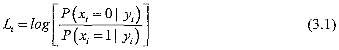
input to a "soft" decoding algorithm is, for each bit of the codeword, a probability measure that the bit that has been read (or received) is the same as the bit that was written (or transmitted). Often, this probability is expressed as a log likelihood ratio (LLR), i. e. , the logarithm of the ratio of the probability that the bit that was written (or transmitted) was "0" to the probability that the bit that was written (or transmitted) was "1", given the read threshold voltage. Soft decoding algorithms are described e.g. in George C. Clark, Jr. and J. Bibb Cain, Error Correction Coding for Digital Communications (Springer, 1981), in S. Lin and D. J. Costello, Error Control Coding: Fundamentals and Applications (Prentice-Hall, 1983) and in Branka Vucetic and Jinhong Yuan, Turbo Codes: Principles and Applications (Kluwer, 2000).
Heretofore, soft decoding ECC algorithms have been used almost exclusively in contexts other than data storage systems, for example, in signal processing fields such as communications, voice coding and image processing. The majority of academic research on ECC is done in the context of communications. Indeed, the three prior art references cited above on soft decoding are directed at the use of soft ECC algorithms in communication. The ECC decoders of the Ban patent and of the Guterman et al. patent are hard decoders: the soft bits are used only to provide qualitative information about the hard bits. Only recently has the use of soft decoders been proposed, in co-pending US Patent Application Ser. No. 11/514,182, to decode hard bit representations of codewords read from nonvolatile memories such as flash memories. Heretofore, soft decoding has not been used in conjunction with soft bits to decode representations of codewords read from nonvolatile memories such as flash memories.
SUMMARY OF TBDE INVENTION
According to the present invention there is provided a method of reading at least one flash memory cell, including the steps of: (a) for each cell: (i) comparing a threshold voltage of the each cell to at least one integral reference voltage, (ii) comparing the threshold voltage of the each cell to at least one fractional reference voltage, and (iii) based at least in part on outcomes of the comparisons, calculating a respective estimated probability measure of each bit of a bit pattern of the each cell, thereby obtaining a plurality of estimated probability measures; and (b) estimating a respective original bit pattern of each cell, based at least in part on at least two of the estimated probability measures.
According to the present invention there is provided a memory device including: (a) at least one flash memory cell; and (b) a controller operative to read the at least one cell by: (i) for each cell: (A) comparing a threshold voltage of the each cell to at least one integral reference voltage, (B) comparing the threshold voltage of the each cell to at least one fractional reference voltage, and (C) based at least in part on outcomes of the comparisons, calculating a respective estimated probability measure of each bit of a bit pattern of the each cell, thereby obtaining a plurality of estimated probability measures, and (ii) estimating a respective original bit pattern of each cell, based at least in part on at least two of the estimated probability measures. According to the present invention there is provided a system including: (a) a memory device that includes at least one flash memory cell; and (b) a processor operative to read the at least one cell by: (i) for each cell: (A) comparing a threshold voltage of the each cell to at least one integral reference voltage, (B) comparing the threshold voltage of the each cell to at least one fractional reference voltage, and (C) based at least in part on outcomes of the comparisons, calculating a respective
estimated probability measure of each bit of a bit pattern of the each cell, thereby obtaining a plurality of estimated probability measures, and (ii) estimating a respective original bit pattern of each cell, based at least in part on at least two of the estimated probability measures. The basic method of the present invention is a method of reading one or more cells of a flash memory. Each cell's threshold voltage is compared to at least one integral reference voltage and to at least one fractional reference voltage. Based at least in part on the outcomes of those comparisons, a respective estimated probability measure of each bit of a bit pattern of the cell is calculated. This respective estimated probability measure can be e.g. the probability itself that the bit originally was written to the cell as "0", or the probability itself that the bit originally was written to the cell as "1", or a LLR that expresses the likelihood of the bit originally having been written as "0" or "1", or other probability measures as discussed below. In the case of a SLC, there is only one bit in the bit pattern. In the case of a MLC, there are two or more bits in the bit pattern.
The result of this estimating is a plurality of estimated probability measures. It is important to note that the scope of the invention does not include the case of comparing the threshold voltage of a single SLC, considered in isolation, to V1 and to one or more fractional reference voltages, and then estimating a single probability measure. Finally, the original bit pattern(s) of the cell(s)5 i.e., the bit pattern(s) originally stored in the cell(s), is/are estimated, based at least in part on at least two of the estimated probability measures.
Typically, as in the case of MLCs, the threshold voltage(s) is/are compared to a plurality of integral reference voltages.
Preferably, the estimated probability measures are initial estimated probability measures, which means that the estimated probability measures are input to the step of estimating the original bit pattern(s) rather than intermediate results of the estimation of the original bit pattern(s). More preferably, the estimating of the original bit pattern(s) includes transforming the initial estimated probability measures to final estimated probability measures. Most preferably, transforming the initial estimated probability measures into the final estimated probability measures is constrained by requiring the original bit pattem(s) to constitute, when taken together as a single unit, a member of a set of candidates, e.g. a member of a set of codewords. Also most preferably, the estimating of the original bit pattern(s) is based on the final estimated probability measures.
Preferred methods of estimating the original bit pattern(s) include maximum a- posteriori probability decoding and maximum likelihood decoding. Preferred examples of maximum likelihood decoding include maximum likelihood sequence estimation decoding and reduced-set maximum likelihood sequence estimation decoding.
Preferably, the original bit patterns are estimated iteratively, e.g. by using iterative decoding techniques. Such iterative decoding techniques often employ maximum a-posteriori probability decoders, or maximum likelihood decoders, with message-passing algorithms.
Preferably, the estimating of the original bit pattern(s) is with reference to a set of candidates. Most preferably, the estimating of the original bit pattern(s) includes assigning a respective metric to each member of the set of candidates, as in maximum likelihood decoding. Also most preferably, the candidates are codewords that could have been used to encode the information originally stored in the cells. This is
because, typically, the bit pattern(s) originally stored in the cells are portions of such codewords or even (in the case of sufficiently short codewords and MLCs with enough levels) entire such codewords. Therefore, the estimating of the original bit pattern(s) often assumes that the original bit pattern(s) included one or more such codewords. The possibility (in principle: this mode of operation is not presently a preferred mode of operation) of storing an entire codeword in a single MLC is the reason that the scope of the present invention includes applying the method of the present invention to even a single flash memory cell.
Preferably, the estimating of the original bit pattern(s) includes assigning a respective metric to each bit of each bit pattern. For example, in the MAP algorithm discussed below, each bit is assigned a decision criterion £),-.
Preferably, the estimation of the original bit pattern(s) is based at least in part on all of the estimated probability measures.
Preferably, the method of the present invention also includes a preliminary step of providing a flash model for the flash memory cell(s). The calculation of the estimated probabilities is in accordance with the flash model. Most preferably, the flash model includes a crossover probability matrix that defines the probability of reading any of the values corresponding to the threshold voltage bands, given any programmed voltage level value. The scope of the present invention also includes a memory device that includes one or more flash memory cells and a controller that reads the cell(s) using the method of the present invention. The scope of the present invention also includes a system that includes a memory device that includes one or more flash memory cells and a processor that reads the cell(s) using the method of the present invention.
As noted above, the prior art includes US Patent Application Ser. No.
11/514,182 that teaches soft decoding of hard bits. Even if only hard bits are read from flash memory cells, a probability measure for each hard bit can be provided to a soft decoder as a result of mapping each hard bit pattern to its corresponding integral voltage band. The additional use of soft bits, as in the present invention, improves the accuracy of the probability measure and so increases the probability of successfully reconstructing the original codeword for a given number of erroneous bits and increases the number of erroneous bits that can be dealt with a given probability of success.
BRIEF DESCRIPTION OF THE DRAWINGS
The invention is herein described, by way of example only, with reference to the accompanying drawings, wherein:
FIG. 1 illustrates the voltage bands of an eight-level MLC; FIG. 2 is FIG. 1 including fractional reference voltages;
FIG. 3 A illustrates the voltage bands of a collection of SLCs as programmed;
FIG. 3B shows two threshold voltage histograms for the SLCs of FIG. 3 A as read;
FIG. 4 is a high-level block diagram of a flash memory device of the present invention;
FIG. 5 is a high-level partial block diagram of a data storage system of the present invention.
DESCRIPTION OF THE PREFERRED EMBODIMENTS
The principles and operation of a flash memory according to the present invention may be better understood with reference to the drawings and the accompanying description.
Referring now to the drawings, Figure 3 A is an exemplary plot of the threshold voltages of a collection of SLCs as programmed, and Figure 3B shows exemplary histograms of the threshold voltage distributions of the same collection of SLCs, as read, when the SLCs are read much later. (As discussed in US Patent Application Publication No. 2005/0013165, also to Ban, in NAND flash technology, cells are read by being placed on serial bit-lines. Although the read circuitry is able in principle to read the threshold voltage of a single NAND cell, in practice, cells on the bit-line affect the value read and limit the accuracy with which the value can be read. This is why some SLCs that were left unprogrammed could be read as though then- threshold voltages exceed V1.)
In Figure 3B, each threshold voltage range is labeled with the corresponding single hard bit and two soft bits shown as a three-bit binary number whose most significant bit is the hard bit and whose two least significant bits are the soft bits. The following table shows how a measured threshold voltage V is interpreted in terms of hard and soft bits:

histogram of threshold voltage probabilities for cells initially programmed to "1". In tabular form, the histograms are, for cells initially programmed to "0":


Note that the two histograms are mirror images of each other.
Figure 3 B is a pictorial representation of the following crossover probability matrix. The first row of the matrix is the probability of writing "0" and reading any of
the eight possible values of the hard bit and the two soft bits. The second row of the
matrix is the probability of writing "1" and reading any of the eight possible values of the hard bit and the two soft bits. The second row is the mirror image of the first row.
(O.005 0.015 0.03 0.05 0.10 0.18 0.40 0.22 ^j I 0.22 0.40 0.18 0.10 0.05 0.03 0.015 0.005 )
An example of the use of four of these cells to store two data bits now is presented. The data bits are encoded using a rate V2 systematic linear code with four codewords as shown in the following table:

The Theory Section presents a Maximum A-posteriori Probability (MAP) algorithm for estimating which member of a set C of codewords was programmed into a set of SLCs, given a set χ of bits (hard bits or both hard and soft bits) read from the SLCs and probabilities P(y,\x,), for reading, from the z-th SLC, the hard bit plus zero or more soft bits y, given that the corresponding SLC was programmed to X1. Note that X1 can be either "0" or "1" and that
 Specifically, according to the Theory Section, to an initial conditional LLR,
 is added extrinsic information E1 based on the codeword set C to give a decision criterion D1. The resulting estimate X1 of the bit originally written to the z-th SLC is
"0" if A>0 and "1" otherwise.
Now consider four SLCs to which the codeword 1111 (i.e.,
 has been written and whose threshold voltages V are measured as follows:
Vl<Vl<Vi25
V0 75<V2<Vi
Vθ 5<V4<VO 75
If the V had been measured only relative to the single integral reference voltage V1, only the hard bits yi=0, yχ=l, J3~l and ^4=I would have been read. The associated conditional probabilities are the same for all four SLCs:
 algorithm of the Theory section then gives:

The estimated written codeword, 0101, differs from the true written codeword, 1111, in two bits, and so is an even worse estimate of the true written codeword than the hard bits as read. The resulting estimate of the encoded data bits is "01" which is incorrect. But having measured the V relative to the fractional reference voltages gives the following hard and soft read bits and associated conditional probabilities:

The MAP algorithm of the Theory section now gives:

The MAP algorithm of the Theory Section is only exemplary. Those skilled in the art will recognize how to implement the present invention using any suitable algorithm, for example a maximum likelihood algorithm or a maximum likelihood sequence estimation algorithm or a reduced-set maximum likelihood sequence estimation algorithm. Examples of a reduced-set maximum likelihood sequence estimation algorithm are found in Fragiacomo et al., "Novel near maximum likelihood soft decision decoding algorithm for linear block codes", IEEE, pp. 265-270, October 1999 and in US Patent No. 6,418,172 to Raghavan.
Figure 4 is a high-level block diagram of a flash memory device 30 of the present invention, coupled to a host 40. Figure 4 is adapted from Figure 1 of Ban, US Patent No. 5,404,485, which patent is incorporated by reference for all purposes as if fully set forth herein. Flash memory device 30 includes a flash memory 34, a controller 32 and a random access memory (RAM) 36. Controller 32, that corresponds to "flash control 14" of US 5,404,485, manages flash memory 34, with the help of RAM 36, as described in US 5,404,485. Controller 32 also supports error correction of data read from flash memory 34 as described above.
Figure 5 is a high-level partial block diagram of an alternative data storage system 60 of the present invention. Data storage system 60 includes a processor 62 and four memory devices: a RAM 64, a boot ROM 66, a mass storage device (hard disk) 68 and a flash memory device 50, all communicating via a common bus 70. Like flash memory device 30 of Figure 4, flash memory device 50 includes a flash memory 52. Unlike flash memory device 30 of Figure 4, flash memory device 50 lacks its own controller and RAM. Instead, processor 62 emulates controller 32 of Figure 4 by executing a software driver that implements the methodology of US 5,404,485 in the manner e.g. of the TrueFFS™ driver of msystems Ltd. of Kfar Saba, Israel, and that also implements the error correction methodology of the present invention. Flash memory device also includes a bus interface 54 to enable processor 62 to communicate with flash memory 52.
While the invention has been described with respect to a limited number of embodiments, it will be appreciated that many variations, modifications and other applications of the invention may be made.
THEORY SECTION
Denote a single written bit as 'x1 and a single read value as ey\ The set of 4 written bits is denoted 'x' and the set of 4 read values is denoted as 'j/'.
We consider the MAP decoder i.e. a decoder that receives some initial estimates for each of the bits and then updates the initial estimates according to the code. The MAP decoder calculates:
Vi e {1,2,3,4} calculate
 c) (0.1)
Here ' C ' denotes the code employed and 'j;' denotes the received sequence of read values. Now the decision for each bit is according to:

Note that:

We can replace (0.2) with:

D,

And our decision rule is therefore summarized to:


Using (0.7) formula (0.5) becomes:
D1

It is easy to see that in the right side of (0.8) the term P(y \ C) is reduced; therefore
(0.8) is simplified to:
D, =

Assuming the information received is symmetric, i.e. the number of ones and the number of zeros to encode are equal on average then for any linear code:

Note that if the information received is not symmetric, the processor can be implemented with scrambling and descrambling units to symmetrize the information. Using (1.1) equation (0.9) becomes:
D1

In (1.2) the term P[y | x, = 0 , C) means the probability of receiving sequence cyj for all code words in ' C with '0' in bit '/'. Mathematically, this term is defined as follows:

Assuming the FLASH'S cells are independent from one another then:

In both (1.3) and (1.4) 'xf is element 'f in vector ex' and 1^f is element '/' in vector 'jf. 'N' is the number of bits in the code: 4 in our case. Introducing (1.4) and (1.3) to (1.2) we get:

Using the fact that in the nominator of (1.5) in all code words at location T bit 'x' is zero (x,=0) we can re- write the nominator of (1.5) as follows:

Introducing (1.6) into (1.5) and employing the same for the denominator we get:
D1 =

We define:

D = L, + E. (1.9)
We now continue to further develop L1 and E1. Going back to 'Bayes' Law' we re-write L1 as follows:

Introducing (1.1) into (2.1) we get that:
L1

From (2.2) we learn that in our case L1 is the initial estimation for bit T regardless of the code, even though L, is calculated via (1.8) in practice. And therefore E1 is the extrinsic information, meaning the update to the initial estimation L1 obtained from the decoding process.
Using (0.3) and L1 as in (2.2) we conclude that L1 (the LLR) is bijective with the probability P(x, = 01 yt) as follows:
Now assuming that bit xρl was written but the decoder has decided erroneously that 5c, = 0 , the probability of this error is:

Equation (2.4) can be re- written as follows:

Summary:
I. A priori information fed to the decoder:
- The possible code words that could have been written.
» The flash model, i.e. P (>>, | x;) for any possible 'j>' and xe {0,1 }.
II. Decoding:
* For each bit the algorithm receives '.£' the set of values read from the flash. In the event of soft bits 'j;' includes more than 1 bit for each value 'y\
■ From cjj/' a set of initial LLR estimations L are composed. For bit T L1 is:
» Given 'j>' , and the a priori information, an update D1 for bit T is calculated as follows:

A decision whether bit '/' is '1' or '0' is taken as follows: to if D1 ≥ 0 x. =< (3-3) 1 else
The probability of error in decoding for the specific bit is:
P. (0 (3.4)

Claims
1. A method of reading at least one flash memory cell, comprising the steps of:
(a) for each cell:
(i) comparing a threshold voltage of said each cell to at least one integral reference voltage, (ii) comparing said threshold voltage of said each cell to at least one fractional reference voltage, and (iii) based at least in part on outcomes of said comparisons, calculating a respective estimated probability measure of each bit of a bit pattern of said each cell, thereby obtaining a plurality of estimated probability measures; and
(b) estimating a respective original bit pattern of each cell, based at least in part on at least two of said estimated probability measures.
2. The method of claim 1, wherein, for each cell, said threshold voltage of said each cell is compared to a plurality of integral reference voltages.
3. The method of claim 1, wherein said estimated probability measures are initial estimated probability measures.
4. The method of claim 3, wherein said estimating of said at least one original bit pattern includes Ixansforming said initial estimated probability measures into final estimated probability measures.
5. The method of claim 4, wherein said transforming is constrained by said at least one original bit pattern collectively being a member of a set of candidates.
6. The method of claim 5, wherein said candidates are codewords.
7. The method of claim 4, wherein said estimating of said at least one original bit pattern is based on said final estimated probability measures.
8. The method of claim I5 wherein said estimating of said at least one original bit pattern includes maximum a-posteriori probability decoding.
9. The method of claim 1, wherein said estimating of said at least one original bit pattern includes maximum likelihood decoding.
10. .The method of claim 9, wherein said maximum likelihood decoding includes maximum likelihood sequence estimation decoding.
11. The method of claim 10, wherein said maximum likelihood sequence estimation decoding includes reduced set maximum likelihood sequence estimation decoding.
12. The method of claim 1 , wherein said estimating is effected iteratively.
13. The method of claim 1, wherein said estimating of said at least one original bit pattern is with reference to a set of candidates.
14. The method of claim 13, wherein said estimating of said at least one original bit pattern includes assigning a respective metric to each member of said set of candidates.
15. The method of claim 13, wherein said candidates are codewords.
16. The method of claim 1, wherein said estimating of said at least one original bit pattern includes assigning a respective metric to each said bit of said at least one bit pattern.
17. The method of claim 1 , wherein said estimating is based at least in part on all said estimated probability measures.
18. The method of claim 1 , further comprising the step of:
(c) providing a flash model for the at least one cell, said calculating of said estimated probability measures then being in accordance with said flash model.
19. The method of claim 18, wherein said flash model includes a crossover probability matrix.
20. A memory device comprising:
(a) at least one flash memory cell; and
(b) a controller operative to read said at least one cell by: (i) for each said cell: (A) comparing a threshold voltage of said each cell to at least one integral reference voltage,
(B) comparing said threshold voltage of said each cell to at least one fractional reference voltage, and
(C) based at least in part on outcomes of said comparisons, calculating a respective estimated probability measure of each bit of a bit pattern of said each cell, thereby obtaining a plurality of estimated probability measures, and
(ii) estimating a respective original bit pattern of each said cell, based at least in part on at least two of said estimated probability measures.
21. A system comprising:
(a) a memory device that includes at least one flash memory cell; and
(b) a processor operative to read said at least one cell by: (i) for each said cell:
(A) comparing a threshold voltage of said each cell to at least one integral reference voltage,
(B) comparing said threshold voltage of said each cell to at least one fractional reference voltage, and
(C) based at least in part on outcomes of said comparisons, calculating a respective estimated probability measure of each bit of a bit pattern of said each cell, thereby obtaining a plurality of estimated probability measures, and
(ii) estimating a respective original bit pattern of each said cell, based at least in part on at least two of said estimated probability measures.
Priority Applications (1)
| Application Number | Priority Date | Filing Date | Title |
|---|---|---|---|
| KR1020097009741A KR101458441B1 (en) | 2006-12-21 | 2007-12-19 | Soft decoding of hard and soft bits read from a flash memory |
Applications Claiming Priority (2)
| Application Number | Priority Date | Filing Date | Title |
|---|---|---|---|
| US11/642,708 | 2006-12-21 | ||
| US11/642,708 US7814401B2 (en) | 2006-12-21 | 2006-12-21 | Soft decoding of hard and soft bits read from a flash memory |
Publications (2)
| Publication Number | Publication Date |
|---|---|
| WO2008075351A2 true WO2008075351A2 (en) | 2008-06-26 |
| WO2008075351A3 WO2008075351A3 (en) | 2008-07-31 |
Family
ID=39271218
Family Applications (1)
| Application Number | Title | Priority Date | Filing Date |
|---|---|---|---|
| PCT/IL2007/001565 WO2008075351A2 (en) | 2006-12-21 | 2007-12-19 | Soft decoding of hard and soft bits read from a flash memory |
Country Status (4)
| Country | Link |
|---|---|
| US (1) | US7814401B2 (en) |
| KR (1) | KR101458441B1 (en) |
| TW (1) | TWI364763B (en) |
| WO (1) | WO2008075351A2 (en) |
Cited By (7)
| Publication number | Priority date | Publication date | Assignee | Title |
|---|---|---|---|---|
| US8406048B2 (en) | 2008-08-08 | 2013-03-26 | Marvell World Trade Ltd. | Accessing memory using fractional reference voltages |
| CN103106924A (en) * | 2011-09-29 | 2013-05-15 | 三星电子株式会社 | Method of reading memory cells with different threshold voltages without variation of word line voltage and nonvolatile memory device using the same |
| WO2013070493A1 (en) * | 2011-11-10 | 2013-05-16 | Sandisk Technologies Inc. | Method and apparatus to provide data including hard bit data and soft bit data to a rank modulation decoder |
| EP2763042A1 (en) * | 2013-01-31 | 2014-08-06 | LSI Corporation | Detection and decoding in flash memories with selective binary and non-binary decoding |
| GB2513592A (en) * | 2013-04-30 | 2014-11-05 | Ibm | Read-detection in multi-level cell memory |
| US9086984B2 (en) | 2011-01-04 | 2015-07-21 | Seagate Technology Llc | Detection and decoding in flash memories with selective binary and non-binary decoding |
| US9268635B2 (en) | 2014-05-21 | 2016-02-23 | Sandisk Technologies Inc. | Error correction using multiple data sources |
Families Citing this family (75)
| Publication number | Priority date | Publication date | Assignee | Title |
|---|---|---|---|---|
| US7904793B2 (en) * | 2007-03-29 | 2011-03-08 | Sandisk Corporation | Method for decoding data in non-volatile storage using reliability metrics based on multiple reads |
| US7966550B2 (en) * | 2007-03-31 | 2011-06-21 | Sandisk Technologies Inc. | Soft bit data transmission for error correction control in non-volatile memory |
| US7966546B2 (en) * | 2007-03-31 | 2011-06-21 | Sandisk Technologies Inc. | Non-volatile memory with soft bit data transmission for error correction control |
| US7971127B2 (en) * | 2007-03-31 | 2011-06-28 | Sandisk Technologies Inc. | Guided simulated annealing in non-volatile memory error correction control |
| US7975209B2 (en) * | 2007-03-31 | 2011-07-05 | Sandisk Technologies Inc. | Non-volatile memory with guided simulated annealing error correction control |
| KR101397549B1 (en) * | 2007-08-16 | 2014-05-26 | 삼성전자주식회사 | Non-volatile semiconductor memory device and system capable of fast rogramming and read method thereof |
| WO2009072103A2 (en) * | 2007-12-05 | 2009-06-11 | Densbits Technologies Ltd. | Flash memory apparatus and methods using a plurality of decoding stages including optional use of concatenated bch codes and/or designation of 'first below' cells |
| KR20090097673A (en) * | 2008-03-12 | 2009-09-16 | 삼성전자주식회사 | Apparatus for detecting memory data based on soft decision value |
| US8533563B2 (en) * | 2008-03-31 | 2013-09-10 | Qimonda Ag | Memory read-out |
| KR101506655B1 (en) * | 2008-05-15 | 2015-03-30 | 삼성전자주식회사 | Memory device and method of managing memory data error |
| CN102132350B (en) * | 2008-07-01 | 2015-06-17 | Lsi公司 | Methods and apparatus for soft demapping and intercell interference mitigation in flash memories |
| JP5535219B2 (en) * | 2008-09-30 | 2014-07-02 | エルエスアイ コーポレーション | Method and apparatus for soft data generation in a memory device using a reference cell |
| US7995387B2 (en) * | 2009-01-30 | 2011-08-09 | Sandisk Il Ltd. | System and method to read data subject to a disturb condition |
| US8374026B2 (en) * | 2009-01-30 | 2013-02-12 | Sandisk Il Ltd. | System and method of reading data using a reliability measure |
| US8458114B2 (en) * | 2009-03-02 | 2013-06-04 | Analog Devices, Inc. | Analog computation using numerical representations with uncertainty |
| US20100220514A1 (en) * | 2009-03-02 | 2010-09-02 | Lyric Semiconductor, Inc. | Storage devices with soft processing |
| US8107306B2 (en) | 2009-03-27 | 2012-01-31 | Analog Devices, Inc. | Storage devices with soft processing |
| US8255773B2 (en) * | 2009-06-29 | 2012-08-28 | Sandisk Technologies Inc. | System and method of tracking error data within a storage device |
| KR101618311B1 (en) * | 2010-02-08 | 2016-05-04 | 삼성전자주식회사 | Flash memory device and reading method thereof |
| US8429500B2 (en) | 2010-03-31 | 2013-04-23 | Lsi Corporation | Methods and apparatus for computing a probability value of a received value in communication or storage systems |
| US8504885B2 (en) | 2010-03-31 | 2013-08-06 | Lsi Corporation | Methods and apparatus for approximating a probability density function or distribution for a received value in communication or storage systems |
| US8775913B2 (en) | 2010-03-31 | 2014-07-08 | Lsi Corporation | Methods and apparatus for computing soft data or log likelihood ratios for received values in communication or storage systems |
| TWI633557B (en) | 2010-04-19 | 2018-08-21 | 慧榮科技股份有限公司 | Method for performing memory access management, and associated memory device and controller thereof |
| US11869584B2 (en) | 2010-04-19 | 2024-01-09 | Silicon Motion, Inc. | Memory access module for performing a plurality of sensing operations to generate digital values of a storage cell in order to perform decoding of the storage cell |
| KR101672293B1 (en) | 2010-05-11 | 2016-11-03 | 삼성전자주식회사 | Non-volatile memory device, read operation method thereof, and devices having the same |
| TWI455132B (en) * | 2010-06-23 | 2014-10-01 | Phison Electronics Corp | Data reading method and control circuit and memory controller using the same |
| US9898361B2 (en) | 2011-01-04 | 2018-02-20 | Seagate Technology Llc | Multi-tier detection and decoding in flash memories |
| US9292377B2 (en) | 2011-01-04 | 2016-03-22 | Seagate Technology Llc | Detection and decoding in flash memories using correlation of neighboring bits and probability based reliability values |
| US9502117B2 (en) * | 2011-03-14 | 2016-11-22 | Seagate Technology Llc | Cell-level statistics collection for detection and decoding in flash memories |
| US8880977B2 (en) | 2011-07-22 | 2014-11-04 | Sandisk Technologies Inc. | Systems and methods of storing data |
| JP2013080450A (en) * | 2011-09-22 | 2013-05-02 | Toshiba Corp | Memory device |
| GB2509858B (en) | 2011-09-29 | 2015-08-26 | Ibm | Read-detection in solid-state storage devices |
| KR101919902B1 (en) | 2011-10-18 | 2018-11-20 | 삼성전자 주식회사 | Method of reading data in memory device |
| US8788889B2 (en) | 2011-11-23 | 2014-07-22 | Sandisk Technologies Inc. | Bit stream aliasing in memory system with probabilistic decoding |
| US8644067B2 (en) | 2011-11-30 | 2014-02-04 | Sandisk Technologies Inc. | Systems and methods of decoding data using soft bits at a non-binary decoder that uses probabilistic decoding |
| US8787079B2 (en) * | 2012-05-07 | 2014-07-22 | Sandisk Technologies Inc. | Reading data from multi-level cell memory |
| US9064575B2 (en) | 2012-08-03 | 2015-06-23 | Micron Technology, Inc. | Determining whether a memory cell state is in a valley between adjacent data states |
| US9239754B2 (en) * | 2012-08-04 | 2016-01-19 | Seagate Technology Llc | Single read based soft-decision decoding of non-volatile memory |
| US8732537B2 (en) * | 2012-08-06 | 2014-05-20 | Lsi Corporation | Method and system for symbol error rate estimation and sector quality measurement |
| US20140071761A1 (en) | 2012-09-10 | 2014-03-13 | Sandisk Technologies Inc. | Non-volatile storage with joint hard bit and soft bit reading |
| US9136001B2 (en) | 2012-10-22 | 2015-09-15 | Apple Inc. | Signal-to-Noise Ratio (SNR) estimation in analog memory cells based on optimal read thresholds |
| US9159407B2 (en) * | 2012-10-22 | 2015-10-13 | Apple Inc. | Soft readout from analog memory cells in the presence of read threshold errors |
| US9190174B2 (en) | 2012-11-30 | 2015-11-17 | Micron Technology, Inc. | Determining soft data from a hard read |
| KR102125371B1 (en) | 2012-12-04 | 2020-06-22 | 삼성전자주식회사 | non- volatile memory device and operating method thereof |
| KR102083491B1 (en) | 2012-12-05 | 2020-03-02 | 삼성전자 주식회사 | Memory device, memory system and operating method of the same |
| US9116822B2 (en) | 2012-12-07 | 2015-08-25 | Micron Technology, Inc. | Stopping criteria for layered iterative error correction |
| US9015554B2 (en) | 2012-12-20 | 2015-04-21 | Seagate Technology Llc | Management of non-valid decision patterns of a soft read retry operation |
| US9229848B2 (en) | 2013-01-21 | 2016-01-05 | Micron Technology, Inc. | Determining soft data for fractional digit memory cells |
| US9065483B2 (en) | 2013-01-21 | 2015-06-23 | Micron Technology, Inc. | Determining soft data using a classification code |
| US9728263B2 (en) | 2013-05-31 | 2017-08-08 | Sandisk Technologies Llc | Method and device for iteratively updating read voltages |
| US10475523B2 (en) | 2013-05-31 | 2019-11-12 | Western Digital Technologies, Inc. | Updating read voltages triggered by the rate of temperature change |
| US9697905B2 (en) | 2013-05-31 | 2017-07-04 | Sandisk Technologies Llc | Updating read voltages using syndrome weight comparisons |
| US9298552B2 (en) | 2013-09-27 | 2016-03-29 | Intel Corporation | Using read values from previous decoding operations to calculate soft bit information in an error recovery operation |
| US9021154B2 (en) | 2013-09-27 | 2015-04-28 | Intel Corporation | Read training a memory controller |
| GB2520708A (en) | 2013-11-28 | 2015-06-03 | Ibm | Multi-stage codeword detector |
| TWI541819B (en) | 2013-12-30 | 2016-07-11 | 慧榮科技股份有限公司 | Method for performing error correction, and associated memory apparatus thereof and associated controller thereof |
| KR102149668B1 (en) | 2014-04-22 | 2020-08-31 | 삼성전자주식회사 | Data decoding method of Non-volatile memory device |
| US9213602B1 (en) * | 2014-06-23 | 2015-12-15 | Seagate Technology Llc | Write mapping to mitigate hard errors via soft-decision decoding |
| US20160080004A1 (en) * | 2014-09-11 | 2016-03-17 | Kabushiki Kaisha Toshiba | Memory controller and decoding method |
| CN105468471A (en) * | 2014-09-12 | 2016-04-06 | 光宝科技股份有限公司 | Solid state storage device and error correction method thereof |
| US9678832B2 (en) | 2014-09-18 | 2017-06-13 | Sandisk Technologies Llc | Storage module and method for on-chip copy gather |
| US9406377B2 (en) | 2014-12-08 | 2016-08-02 | Sandisk Technologies Llc | Rewritable multibit non-volatile memory with soft decode optimization |
| US9780809B2 (en) | 2015-04-30 | 2017-10-03 | Sandisk Technologies Llc | Tracking and use of tracked bit values for encoding and decoding data in unreliable memory |
| US9720612B2 (en) | 2015-04-30 | 2017-08-01 | Sandisk Technologies Llc | Biasing schemes for storage of bits in unreliable storage locations |
| US9836351B2 (en) * | 2016-03-21 | 2017-12-05 | Nandext Srl | Method for decoding bits in a solid state drive, and related solid state drive |
| US10423492B2 (en) | 2016-05-17 | 2019-09-24 | SK Hynix Inc. | Self error-handling flash memory device |
| TWI584304B (en) * | 2016-05-23 | 2017-05-21 | 大心電子(英屬維京群島)股份有限公司 | Decoding method, memory storage device and memory control circuit unit |
| US10025661B1 (en) | 2016-12-27 | 2018-07-17 | Sandisk Technologies Llc | Adaptive hard and soft bit decoding |
| US10382067B2 (en) | 2017-06-08 | 2019-08-13 | Western Digital Technologies, Inc. | Parameterized iterative message passing decoder |
| US10418097B2 (en) | 2017-11-27 | 2019-09-17 | Western Digital Technologies, Inc. | Non-volatile storage system with read calibration |
| US10304550B1 (en) | 2017-11-29 | 2019-05-28 | Sandisk Technologies Llc | Sense amplifier with negative threshold sensing for non-volatile memory |
| US10908986B2 (en) | 2018-04-02 | 2021-02-02 | Sandisk Technologies Llc | Multi-level recovery reads for memory |
| US10811091B2 (en) | 2018-10-12 | 2020-10-20 | Western Digital Technologies, Inc. | Adaptive processing for read threshold voltage calibration |
| US10643695B1 (en) | 2019-01-10 | 2020-05-05 | Sandisk Technologies Llc | Concurrent multi-state program verify for non-volatile memory |
| US11024392B1 (en) | 2019-12-23 | 2021-06-01 | Sandisk Technologies Llc | Sense amplifier for bidirectional sensing of memory cells of a non-volatile memory |
Citations (5)
| Publication number | Priority date | Publication date | Assignee | Title |
|---|---|---|---|---|
| US6279133B1 (en) * | 1997-12-31 | 2001-08-21 | Kawasaki Steel Corporation | Method and apparatus for significantly improving the reliability of multilevel memory architecture |
| EP1137001A1 (en) * | 2000-03-23 | 2001-09-26 | Sony Corporation | Reproduction of recorded data using a soft input/soft output demodulator |
| US20030217323A1 (en) * | 2002-05-20 | 2003-11-20 | Sandisk Corporation | Increasing the effectiveness of error correction codes and operating multi-level memory systems by using information about the quality of the stored data |
| WO2004112040A2 (en) * | 2003-06-17 | 2004-12-23 | M-Systems Flash Disk Pioneers Ltd. | Methods of increasing the reliability of a flash memory |
| WO2008042593A1 (en) * | 2006-09-28 | 2008-04-10 | Sandisk Corporation | Nonvolatile memory with error correction based on the likehood the error may occur |
Family Cites Families (5)
| Publication number | Priority date | Publication date | Assignee | Title |
|---|---|---|---|---|
| US5404485A (en) | 1993-03-08 | 1995-04-04 | M-Systems Flash Disk Pioneers Ltd. | Flash file system |
| US6418172B1 (en) | 1999-04-21 | 2002-07-09 | National Semiconductor Corporation | Look-ahead maximum likelihood sequence estimation decoder |
| US7023735B2 (en) | 2003-06-17 | 2006-04-04 | Ramot At Tel-Aviv University Ltd. | Methods of increasing the reliability of a flash memory |
| US20070266296A1 (en) * | 2006-05-15 | 2007-11-15 | Conley Kevin M | Nonvolatile Memory with Convolutional Coding |
| US7805663B2 (en) * | 2006-09-28 | 2010-09-28 | Sandisk Corporation | Methods of adapting operation of nonvolatile memory |
-
2006
- 2006-12-21 US US11/642,708 patent/US7814401B2/en not_active Expired - Fee Related
-
2007
- 2007-12-19 WO PCT/IL2007/001565 patent/WO2008075351A2/en active Application Filing
- 2007-12-19 KR KR1020097009741A patent/KR101458441B1/en not_active IP Right Cessation
- 2007-12-20 TW TW096149087A patent/TWI364763B/en not_active IP Right Cessation
Patent Citations (5)
| Publication number | Priority date | Publication date | Assignee | Title |
|---|---|---|---|---|
| US6279133B1 (en) * | 1997-12-31 | 2001-08-21 | Kawasaki Steel Corporation | Method and apparatus for significantly improving the reliability of multilevel memory architecture |
| EP1137001A1 (en) * | 2000-03-23 | 2001-09-26 | Sony Corporation | Reproduction of recorded data using a soft input/soft output demodulator |
| US20030217323A1 (en) * | 2002-05-20 | 2003-11-20 | Sandisk Corporation | Increasing the effectiveness of error correction codes and operating multi-level memory systems by using information about the quality of the stored data |
| WO2004112040A2 (en) * | 2003-06-17 | 2004-12-23 | M-Systems Flash Disk Pioneers Ltd. | Methods of increasing the reliability of a flash memory |
| WO2008042593A1 (en) * | 2006-09-28 | 2008-04-10 | Sandisk Corporation | Nonvolatile memory with error correction based on the likehood the error may occur |
Non-Patent Citations (1)
| Title |
|---|
| IEEE TRANSACTIONS ON INFORMATION THEORY, vol. 22, no. 5, September 1976 (1976-09), pages 514-517, XP002480327 cited in the application * |
Cited By (12)
| Publication number | Priority date | Publication date | Assignee | Title |
|---|---|---|---|---|
| US8406048B2 (en) | 2008-08-08 | 2013-03-26 | Marvell World Trade Ltd. | Accessing memory using fractional reference voltages |
| US8867268B2 (en) | 2008-08-08 | 2014-10-21 | Marvell World Trade Ltd. | Accessing memory using reference voltages |
| US9086984B2 (en) | 2011-01-04 | 2015-07-21 | Seagate Technology Llc | Detection and decoding in flash memories with selective binary and non-binary decoding |
| CN103106924A (en) * | 2011-09-29 | 2013-05-15 | 三星电子株式会社 | Method of reading memory cells with different threshold voltages without variation of word line voltage and nonvolatile memory device using the same |
| WO2013070493A1 (en) * | 2011-11-10 | 2013-05-16 | Sandisk Technologies Inc. | Method and apparatus to provide data including hard bit data and soft bit data to a rank modulation decoder |
| US8456919B1 (en) | 2011-11-10 | 2013-06-04 | Sandisk Technologies Inc. | Method and apparatus to provide data including hard bit data and soft bit data to a rank modulation decoder |
| EP2763042A1 (en) * | 2013-01-31 | 2014-08-06 | LSI Corporation | Detection and decoding in flash memories with selective binary and non-binary decoding |
| TWI613674B (en) * | 2013-01-31 | 2018-02-01 | Lsi公司 | Detection and decoding in flash memories with selective binary and non-binary decoding |
| GB2513592A (en) * | 2013-04-30 | 2014-11-05 | Ibm | Read-detection in multi-level cell memory |
| US9305639B2 (en) | 2013-04-30 | 2016-04-05 | International Business Machines Corporation | Read-detection in multi-level cell memory |
| US9619328B2 (en) | 2013-04-30 | 2017-04-11 | International Business Machines Corporation | Read-detection in multi-level cell memory |
| US9268635B2 (en) | 2014-05-21 | 2016-02-23 | Sandisk Technologies Inc. | Error correction using multiple data sources |
Also Published As
| Publication number | Publication date |
|---|---|
| WO2008075351A3 (en) | 2008-07-31 |
| KR101458441B1 (en) | 2014-11-07 |
| US20080151617A1 (en) | 2008-06-26 |
| TWI364763B (en) | 2012-05-21 |
| KR20090101160A (en) | 2009-09-24 |
| TW200836205A (en) | 2008-09-01 |
| US7814401B2 (en) | 2010-10-12 |
Similar Documents
| Publication | Publication Date | Title |
|---|---|---|
| US7814401B2 (en) | Soft decoding of hard and soft bits read from a flash memory | |
| US7533328B2 (en) | Method of error correction in a multi-bit-per-cell flash memory | |
| JP5535219B2 (en) | Method and apparatus for soft data generation in a memory device using a reference cell | |
| US8156403B2 (en) | Combined distortion estimation and error correction coding for memory devices | |
| US9224457B2 (en) | Non-volatile storage with temperature compensation based on neighbor state information | |
| US9990247B2 (en) | Write mapping to mitigate hard errors via soft-decision decoding | |
| US8937838B2 (en) | Finding optimal read thresholds and related voltages for solid state memory | |
| US20080263266A1 (en) | Adaptive dynamic reading of flash memories | |
| JP4999921B2 (en) | Combination of distortion estimation and error correction coding for memory devices. | |
| US9553612B2 (en) | Decoding based on randomized hard decisions | |
| CN112860474B (en) | Soft bit flip decoder for fast converging low density parity check codes | |
| US9082480B2 (en) | Detection and decoding in flash memories with error correlations for a plurality of bits within a sliding window | |
| US9009576B1 (en) | Adaptive LLR based on syndrome weight | |
| CN112331244B (en) | Soft input soft output component code decoder for generalized low density parity check code | |
| CN111049530A (en) | Error correction circuit and method of operating the same | |
| IL196239A (en) | Method of error correction in a multi-bit-per-cell flash memory |
Legal Events
| Date | Code | Title | Description |
|---|---|---|---|
| 121 | Ep: the epo has been informed by wipo that ep was designated in this application |
Ref document number: 07849591 Country of ref document: EP Kind code of ref document: A2 |
|
| WWE | Wipo information: entry into national phase |
Ref document number: 1020097009741 Country of ref document: KR |
|
| NENP | Non-entry into the national phase |
Ref country code: DE |
|
| 122 | Ep: pct application non-entry in european phase |
Ref document number: 07849591 Country of ref document: EP Kind code of ref document: A2 |