WO2007132678A1 - Organic electroluminescent device - Google Patents

Organic electroluminescent device Download PDF

Info

Publication number
WO2007132678A1
WO2007132678A1 PCT/JP2007/059364 JP2007059364W WO2007132678A1 WO 2007132678 A1 WO2007132678 A1 WO 2007132678A1 JP 2007059364 W JP2007059364 W JP 2007059364W WO 2007132678 A1 WO2007132678 A1 WO 2007132678A1
Authority
WO
WIPO (PCT)
Prior art keywords
group
substituted
unsubstituted
layer
carbon atoms
Prior art date
Application number
PCT/JP2007/059364
Other languages
French (fr)
Japanese (ja)
Inventor
Hitoshi Kuma
Hiroshi Yamamoto
Chishio Hosokawa
Original Assignee
Idemitsu Kosan Co., Ltd.
Priority date (The priority date is an assumption and is not a legal conclusion. Google has not performed a legal analysis and makes no representation as to the accuracy of the date listed.)
Filing date
Publication date
Application filed by Idemitsu Kosan Co., Ltd. filed Critical Idemitsu Kosan Co., Ltd.
Priority to EP07742799A priority Critical patent/EP2018090A4/en
Priority to KR1020087027475A priority patent/KR101384046B1/en
Priority to JP2008515489A priority patent/JP5432523B2/en
Priority to US12/300,345 priority patent/US8076839B2/en
Publication of WO2007132678A1 publication Critical patent/WO2007132678A1/en

Links

Classifications

    • HELECTRICITY
    • H10SEMICONDUCTOR DEVICES; ELECTRIC SOLID-STATE DEVICES NOT OTHERWISE PROVIDED FOR
    • H10KORGANIC ELECTRIC SOLID-STATE DEVICES
    • H10K85/00Organic materials used in the body or electrodes of devices covered by this subclass
    • H10K85/60Organic compounds having low molecular weight
    • H10K85/649Aromatic compounds comprising a hetero atom
    • H10K85/654Aromatic compounds comprising a hetero atom comprising only nitrogen as heteroatom
    • HELECTRICITY
    • H10SEMICONDUCTOR DEVICES; ELECTRIC SOLID-STATE DEVICES NOT OTHERWISE PROVIDED FOR
    • H10KORGANIC ELECTRIC SOLID-STATE DEVICES
    • H10K10/00Organic devices specially adapted for rectifying, amplifying, oscillating or switching; Organic capacitors or resistors having a potential-jump barrier or a surface barrier
    • H10K10/40Organic transistors
    • H10K10/46Field-effect transistors, e.g. organic thin-film transistors [OTFT]
    • H10K10/462Insulated gate field-effect transistors [IGFETs]
    • H10K10/484Insulated gate field-effect transistors [IGFETs] characterised by the channel regions
    • H10K10/488Insulated gate field-effect transistors [IGFETs] characterised by the channel regions the channel region comprising a layer of composite material having interpenetrating or embedded materials, e.g. a mixture of donor and acceptor moieties, that form a bulk heterojunction
    • HELECTRICITY
    • H10SEMICONDUCTOR DEVICES; ELECTRIC SOLID-STATE DEVICES NOT OTHERWISE PROVIDED FOR
    • H10KORGANIC ELECTRIC SOLID-STATE DEVICES
    • H10K50/00Organic light-emitting devices
    • H10K50/10OLEDs or polymer light-emitting diodes [PLED]
    • H10K50/14Carrier transporting layers
    • HELECTRICITY
    • H10SEMICONDUCTOR DEVICES; ELECTRIC SOLID-STATE DEVICES NOT OTHERWISE PROVIDED FOR
    • H10KORGANIC ELECTRIC SOLID-STATE DEVICES
    • H10K50/00Organic light-emitting devices
    • H10K50/10OLEDs or polymer light-emitting diodes [PLED]
    • H10K50/19Tandem OLEDs
    • HELECTRICITY
    • H10SEMICONDUCTOR DEVICES; ELECTRIC SOLID-STATE DEVICES NOT OTHERWISE PROVIDED FOR
    • H10KORGANIC ELECTRIC SOLID-STATE DEVICES
    • H10K85/00Organic materials used in the body or electrodes of devices covered by this subclass
    • H10K85/60Organic compounds having low molecular weight
    • H10K85/615Polycyclic condensed aromatic hydrocarbons, e.g. anthracene
    • H10K85/626Polycyclic condensed aromatic hydrocarbons, e.g. anthracene containing more than one polycyclic condensed aromatic rings, e.g. bis-anthracene
    • HELECTRICITY
    • H10SEMICONDUCTOR DEVICES; ELECTRIC SOLID-STATE DEVICES NOT OTHERWISE PROVIDED FOR
    • H10KORGANIC ELECTRIC SOLID-STATE DEVICES
    • H10K85/00Organic materials used in the body or electrodes of devices covered by this subclass
    • H10K85/60Organic compounds having low molecular weight
    • H10K85/631Amine compounds having at least two aryl rest on at least one amine-nitrogen atom, e.g. triphenylamine
    • H10K85/633Amine compounds having at least two aryl rest on at least one amine-nitrogen atom, e.g. triphenylamine comprising polycyclic condensed aromatic hydrocarbons as substituents on the nitrogen atom
    • HELECTRICITY
    • H10SEMICONDUCTOR DEVICES; ELECTRIC SOLID-STATE DEVICES NOT OTHERWISE PROVIDED FOR
    • H10KORGANIC ELECTRIC SOLID-STATE DEVICES
    • H10K85/00Organic materials used in the body or electrodes of devices covered by this subclass
    • H10K85/60Organic compounds having low molecular weight
    • H10K85/649Aromatic compounds comprising a hetero atom
    • H10K85/657Polycyclic condensed heteroaromatic hydrocarbons
    • H10K85/6572Polycyclic condensed heteroaromatic hydrocarbons comprising only nitrogen in the heteroaromatic polycondensed ring system, e.g. phenanthroline or carbazole
    • CCHEMISTRY; METALLURGY
    • C09DYES; PAINTS; POLISHES; NATURAL RESINS; ADHESIVES; COMPOSITIONS NOT OTHERWISE PROVIDED FOR; APPLICATIONS OF MATERIALS NOT OTHERWISE PROVIDED FOR
    • C09KMATERIALS FOR MISCELLANEOUS APPLICATIONS, NOT PROVIDED FOR ELSEWHERE
    • C09K2211/00Chemical nature of organic luminescent or tenebrescent compounds
    • C09K2211/10Non-macromolecular compounds
    • C09K2211/1003Carbocyclic compounds
    • C09K2211/1011Condensed systems
    • CCHEMISTRY; METALLURGY
    • C09DYES; PAINTS; POLISHES; NATURAL RESINS; ADHESIVES; COMPOSITIONS NOT OTHERWISE PROVIDED FOR; APPLICATIONS OF MATERIALS NOT OTHERWISE PROVIDED FOR
    • C09KMATERIALS FOR MISCELLANEOUS APPLICATIONS, NOT PROVIDED FOR ELSEWHERE
    • C09K2211/00Chemical nature of organic luminescent or tenebrescent compounds
    • C09K2211/10Non-macromolecular compounds
    • C09K2211/1018Heterocyclic compounds
    • C09K2211/1022Heterocyclic compounds bridged by heteroatoms, e.g. N, P, Si or B
    • CCHEMISTRY; METALLURGY
    • C09DYES; PAINTS; POLISHES; NATURAL RESINS; ADHESIVES; COMPOSITIONS NOT OTHERWISE PROVIDED FOR; APPLICATIONS OF MATERIALS NOT OTHERWISE PROVIDED FOR
    • C09KMATERIALS FOR MISCELLANEOUS APPLICATIONS, NOT PROVIDED FOR ELSEWHERE
    • C09K2211/00Chemical nature of organic luminescent or tenebrescent compounds
    • C09K2211/10Non-macromolecular compounds
    • C09K2211/1018Heterocyclic compounds
    • C09K2211/1025Heterocyclic compounds characterised by ligands
    • C09K2211/1044Heterocyclic compounds characterised by ligands containing two nitrogen atoms as heteroatoms

Definitions

  • the present invention relates to an organic electoluminescence (EL) device.
  • EL elements using electroluminescence are highly visible due to self-emission and are completely solid elements, and thus have excellent features such as excellent impact resistance. Therefore, as EL elements in various display devices, The use of is attracting attention.
  • This EL device includes an inorganic EL device using an inorganic compound as a light emitting material and an organic EL device using an organic compound.
  • the organic EL device particularly reduces the applied voltage significantly.
  • it since it is easy to achieve full color and surface light emission with low power consumption is possible, it has been developed as a next-generation light-emitting element.
  • Patent Documents 1 to 3 As one of such long-life and high-efficiency technologies, there is a technology in which a plurality of cathode Z organic light emitting layer Z anode units are stacked (for example, Patent Documents 1 to 3). Compared to a single-layer device, the current density is low to obtain the same luminance, and there is an advantage that the device life can be extended. However, these techniques have a problem in that the driving voltage becomes extremely high because a plurality of elements are stacked in series.
  • Patent Document 1 Japanese Patent Laid-Open No. 6-176870
  • Patent Document 2 Japanese Patent Laid-Open No. 11-312584
  • Patent Document 3 Japanese Patent Laid-Open No. 11 312585
  • the present invention has been made in view of the above-described problems, and an object thereof is to provide a high-efficiency and low-voltage organic EL element even when a plurality of light-emitting layers are stacked in series.
  • the following organic EL device is provided.
  • At least two organic light emitting layers are interposed between an anode and a cathode, and the organic light emitting layer There is provided at least one intermediate connection layer therebetween, and the intermediate connection layer includes, from the cathode side, an electron transport material layer including an acceptor layer, a donor layer, and a compound containing a non-complex nitrogen-containing heterocyclic structure in this order.
  • An organic-elect mouth luminescence element is provided.
  • is a hydrogen atom, a substituted or unsubstituted aryl group having 5 to 60 nuclear atoms, a substituted or unsubstituted heteroaryl group having 5 to 60 nuclear atoms, a substituted or unsubstituted group, respectively.
  • An amino group, a halogen atom, a cyano group, a nitro group, a hydroxyl group, or a carboxyl group, substituted with an aryl group having 5 to 50 nuclear atoms, substituted or unsubstituted, and adjacent to A pair is tied together And may form an aromatic ring or a heterocyclic ring.
  • R 9 to R 2 ° are each a hydrogen atom, a substituted or unsubstituted aryl group having 5 to 60 nuclear atoms, a substituted or unsubstituted heteroaryl group having 5 to 60 nuclear atoms, substituted or unsubstituted, An unsubstituted alkyl group having 1 to 50 carbon atoms, a substituted or unsubstituted cycloalkyl group having 3 to 50 carbon atoms, a substituted or unsubstituted aralkyl group having 6 to 50 nuclear atoms, a substituted or unsubstituted carbon number 1 ⁇ 50 alkoxy group, substituted or unsubstituted aryloxy group having 5 to 50 carbon atoms, substituted or unsubstituted aryloxy group having 5 to 50 nucleus atoms, substituted or unsubstituted carbon atoms 1 to 50 An alkoxycarbonyl group, an amino group substituted with a substituted with a
  • (L is a substituted or unsubstituted arylene group having 6 to 60 carbon atoms, a substituted or unsubstituted heteroarylene group having 5 to 60 carbon atoms, or a substituted or unsubstituted fluorenylene group,
  • Ar 1 is a substituted or unsubstituted arylene group having 6 to 60 carbon atoms, a substituted or unsubstituted pyridylene group, or a substituted or unsubstituted quinolylene group,
  • Ar 2 is a hydrogen atom, a substituted or unsubstituted aryl group having 5 to 60 nuclear atoms, a substituted or unsubstituted pyridyl group, a substituted or unsubstituted quinolyl group, a substituted or unsubstituted carbon number of 1 to 50.
  • Donor of the donor layer is alkali metal, alkaline earth metal, rare earth metal, alkali metal oxide, alkali metal halide, alkaline earth metal oxide, alkaline earth metal halide Organic electroluminescence according to any one of 1 to 5, which is a porcelain, rare earth metal oxide, rare earth metal halide, alkali metal organic complex, alkaline earth metal organic complex, and rare earth metal organic complex element.
  • the acceptor force of the acceptor layer The organic electoluminescence element according to any one of 1 to 6, which is an organic compound having an electron-withdrawing substituent or an electron-deficient ring Child.
  • acceptor force of the acceptor layer 7.
  • FIG. 1 is a diagram showing a first embodiment of an organic EL device according to the present invention.
  • FIG. 2 is a view showing an intermediate connection layer of the organic EL element shown in FIG.
  • the organic EL device of the present invention includes at least two organic light emitting layers interposed between an anode and a cathode, and includes at least one intermediate connection layer between the organic light emitting layers.
  • the intermediate connection layer is formed by laminating an acceptor layer, a donor layer, and an electron transport material layer containing a compound containing a non-complex nitrogen-containing heterocyclic structure in this order from the cathode side.
  • FIG. 1 is a view showing an embodiment of the organic EL device of the present invention.
  • This organic EL device is an example in which three organic light emitting layers are laminated.
  • a transparent anode 20 is provided on a support substrate 10, and a cathode 50 is provided opposite to the transparent anode 20.
  • the first organic light emitting layer 30, the second organic light emitting layer 32, the third organic light emitting layer 34, the first intermediate connection layer 40, and the second intermediate light emitting layer 34 are provided between the transparent anode 20 and the cathode 50.
  • a connection layer 42 is provided.
  • the first intermediate connection layer 40 is between the first organic light-emitting layer 30 and the second organic light-emitting layer 32
  • the second intermediate connection layer 42 is the second organic light-emitting layer 32 and the third organic light-emitting layer 32. It is interposed between the light emitting layers 34. Light emitted from the organic light emitting layers 30, 32, and 34 is extracted from the support substrate 10 through the transparent anode 20.
  • FIG. 2 is a diagram showing the intermediate connection layers 40 and 42 of the present invention.
  • the intermediate connection layers 40 and 42 are formed by laminating an acceptor layer 60, a donor layer 70, and an electron transport material layer 80 containing a compound containing a non-complex nitrogen-containing heterocyclic structure in this order from the cathode 50 side.
  • the configuration is as follows.
  • the acceptor layer 60 refers to extracting electrons from an adjacent organic light emitting layer.
  • the donor layer 70 is a layer that receives electrons from the acceptor layer and injects electrons into the electron transport material layer (donates electrons).
  • the electron transport material layer 80 is a layer that injects electrons into the adjacent organic light emitting layer.
  • first organic light emitting layer 30 of the element 1 light is emitted by injecting holes from the anode 20 and injecting electrons from the electron transport material layer of the first intermediate connection layer 40. Electrons are transferred from the acceptor layer to the electron transport material layer of the first intermediate connection layer 40 through the donor layer.
  • the second organic light emitting layer 32 holes are injected from the acceptor layer of the first intermediate connection layer 40, and electrons are injected from the electron transport material layer of the second intermediate connection layer 42. It emits light. Electrons are transferred to the electron transport material layer 80 of the first intermediate connection layer 40 through the donor layer as well as the acceptor layer force. Electrons are transferred from the acceptor layer to the electron transport material layer of the second intermediate connection layer 42 through the donor layer.
  • the acceptor layer force of the second intermediate connection layer 42 also emits light by injecting holes. Electrons are transferred from the acceptor layer to the electron transport material layer 80 of the second intermediate connection layer 42 through the donor layer.
  • the present invention can reduce the voltage by using a specific electron transport material layer for the intermediate connection layer. For this reason, an organic EL element in which organic light emitting layers are stacked is easy to increase the voltage, but even such a stacked organic EL element can achieve a lower voltage and higher efficiency.
  • the three organic light emitting layers 30, 32, 34 and the two intermediate connection layers 40, 42 may be different or the same.
  • three organic light emitting layers are laminated, but two or four or more layers may be laminated. Further, in this embodiment, it is sufficient that there is at least one intermediate connection layer having the laminated structure shown in FIG. 2 between the two organic light emitting layers. Therefore, when there are other organic light-emitting layers, different organic light-emitting layers may be in direct contact with each other and V may be used, or a normal intermediate connection layer may be interposed instead of the laminated structure shown in FIG. ⁇ .
  • the transparent electrode may be a power cathode that is an anode.
  • book The organic EL element of the invention may be a top emission type or a bottom emission type. Even in the case of the V-shift type, the electrode from which light is extracted becomes light transmissive.
  • the support substrate is a member for supporting the organic EL element, and therefore it is preferable that the support substrate is excellent in mechanical strength and dimensional stability.
  • a substrate include a glass plate, a metal plate, a ceramic plate, or a plastic plate (polycarbonate resin, acrylic resin, vinyl chloride resin, polyethylene terephthalate resin, polyimide resin, polyester resin. Resin, epoxy resin, phenol resin, silicon resin, fluorine resin, etc.).
  • the substrate made of these materials is further formed with an inorganic film or coated with fluorine resin to prevent moisture or hydrophobic treatment. Is preferably applied.
  • the moisture content of the support substrate is 0.0001 wt% or less and the gas permeability coefficient is 1 ⁇ 10 ” 13 cc-cm / cm 2 -Sec. CmHg or less.
  • the supporting substrate side force also extracts light
  • anode it is preferable to use a metal, an alloy, an electrically conductive compound, or a mixture thereof having a high work function (for example, 4. OeV or more).
  • a metal, an alloy, an electrically conductive compound, or a mixture thereof having a high work function for example, 4. OeV or more.
  • ITO indium tin oxide
  • IZO indium-zinc oxide
  • indium copper, tin, zinc oxide, gold, platinum, noradium, etc. alone or in combination of two or more Can be used in combination.
  • the anode can be produced by forming a thin film of these electrode materials by a method such as vapor deposition or sputtering. Further, the thickness of the anode is not particularly limited. 1S is preferably 10 to 1000 nm, and more preferably 10 to 200 nm. Further, when taking out the light emitted from the organic light emitting medium layer from the anode to the outside, it is preferable that Is transparent, that is, the light transmittance is 50% or more.
  • the cathode preferably uses a metal, an alloy, an electrically conductive compound or a mixture thereof having a low work function (eg, less than 4. OeV). Specifically, one of magnesium, aluminum, indium, lithium, sodium, cesium, silver and the like can be used alone or in combination of two or more.
  • the thickness of the cathode is not particularly limited, but is preferably 10 to 1000 nm, more preferably 10 to 200 nm.
  • the organic light emitting layer includes an organic light emitting medium layer capable of EL emission by recombination of electrons and holes.
  • Such an organic light emitting layer can be constituted by laminating the following layers, for example.
  • the configuration (iv) is usually preferably used because it can provide higher emission luminance and is excellent in durability.
  • the light emitting medium layer of the organic EL element has the following functions (1) to (3).
  • Injection function Function that can inject holes from the anode or hole injection layer when an electric field is applied, and can inject electrons from the cathode or electron injection layer
  • Transport function Function to move injected charges (electrons and holes) by the force of electric field
  • Luminescent function a function that provides a field for recombination of electrons and holes and connects this to light emission.However, there is no difference between the ease of hole injection and the ease of electron injection.
  • the transport capacity expressed by the mobility of holes and electrons may be large or small, but it is preferable to move one of the charges.
  • the luminescent medium layer is particularly preferably a molecular deposited film.
  • the molecular deposition film is formed by deposition from a material compound in a gas phase state. This is a thin film or a film formed by solidification from a material compound in a solution state or a liquid phase state.
  • this molecular deposited film has a cohesive structure and high structure from a thin film (molecular accumulated film) formed by the LB method. It can be classified by the difference in the next structure and the functional difference resulting from it.
  • a binder such as rosin and a material compound are mixed with a solvent.
  • the light emitting medium layer can also be formed by forming a solution by dissolving the solution in a thin film and then thinly forming the solution by a spin coating method or the like.
  • Examples of the light emitting material or doping material that can be used for the organic light emitting medium layer include arylamine compounds and Z or styrylamine compounds, anthracene, naphthalene, phenanthrene, pyrene, tetracene, coronene, taricene, fluorescein, perylene, and lid-periphery.
  • Lene Naphtha-perylene, Perinone, Lid-perinone, Naphtal-perinone, Diphenylbutadiene, Tetraphenylbutadiene, Coumarin, Oxadiazole, Ardazine, Bisbenzoxazoline, Bisstyryl, Pyrazine, Cyclopentagen, Quinoline metal complex, Aminoquino Phosphorus metal complex, benzoquinoline metal complex, imine, diphenylethylene, berylanthracene, diaminocarbazole, pyran, thiopyran, polymethine, merocyanine, imidazole chelate Examples thereof include, but are not limited to, oxinoid compounds, quinacridone, rubrene, and fluorescent dyes.
  • the organic light emitting medium layer preferably contains an arylamine compound and Z or a styrylamine compound.
  • Examples of the arylamine compounds include compounds represented by the following formula (A), and examples of the styrylamine compounds include compounds represented by the following formula (B).
  • Ar is phenyl, biphenyl, terpheal, stilbene or distyryl aryl
  • Ar 3 2 and Ar 3 3 are each a hydrogen atom or a substituted or unsubstituted carbon number of 6 to 6.
  • 20 is an aromatic group
  • p ′ is an integer of 1 to 4. More preferably, Ar 3 2 and Z or Ar 3 are substituted with a styryl group.
  • the aromatic group having 6 to 20 carbon atoms is preferably a phenyl group, a naphthyl group, an anthracyl group, a phenanthryl group, a terphenyl group, or the like.
  • Ar 3M to Ar 3G6 is a substituted or unsubstituted Ariru group having a carbon number of 5 to 40.
  • Q is an integer from 1 to 4.
  • aryl groups having 5 to 40 nuclear atoms include phenyl, naphthyl, anthracyl, phenanthryl, pyrenyl, chrysenyl, coroninole, biphenyl, terphenyl, pyrrolyl, furanyl, thiophenyl, benzothiophenyl, oxadiazolyl.
  • Diphenylanthracenyl, indolyl, carbazolyl, pyridyl, benzoquinolyl, fluoranthenyl, acenaphthofluoranthur, stilbene and the like are preferable.
  • the aryl group having 5 to 40 nuclear atoms may be further substituted with a substituent.
  • Examples of the preferred substituent include alkyl groups having 1 to 6 carbon atoms (ethyl group, methyl group, isopropyl group, n- Propyl group, s-butyl Group, t-butyl group, pentyl group, hexyl group, cyclopentyl group, cyclohexyl group, etc.), alkoxy group having 1 to 6 carbon atoms (ethoxy group, methoxy group, isopropoxy group, n-portoxy group, s butoxy group, t butoxy group, pentoxy group, hexyloxy group, cyclopentoxy group, cyclohexyloxy group, etc.), aryl group having 5 to 40 nuclear atoms, amino group substituted with aryl group having 5 to 40 nuclear atoms Groups, ester groups having an aryl group having 5 to 40 nuclear atoms, ester groups having an alkyl group having 1 to 6 carbon atoms, cyan groups, nitro groups, hal
  • Ar and Ar ′ are each a substituted or unsubstituted aryl group having 5 to 60 nucleus atoms or a substituted or unsubstituted heteroaryl group having 5 to 60 nucleus atoms.
  • X is substituted or unsubstituted aryl group having 6 to 50 nuclear carbon atoms, substituted or unsubstituted heteroaryl group having 5 to 50 nuclear atoms, substituted or unsubstituted alkyl group having 1 to 50 carbon atoms, substituted Or an unsubstituted alkoxy group having 1 to 50 carbon atoms, a substituted or unsubstituted aralkyl group having 6 to 50 carbon atoms, a substituted or unsubstituted aryloxy group having 5 to 50 nucleus atoms, a substituted or unsubstituted nucleus.
  • a and b are each an integer of 0 to 4.
  • n is an integer of 1 to 3.
  • Ar 1 and Ar 2 are each a substituted or unsubstituted aryl group having 6 to 50 nuclear carbon atoms or a substituted or unsubstituted heteroaryl group having 5 to 60 nuclear atoms.
  • n are each an integer of 1 to 4.
  • R ⁇ R 10 ⁇ each hydrogen atom, substituted or unsubstituted aryl group having 6 to 50 nuclear carbon atoms, substituted or unsubstituted heteroaryl group having 5 to 50 nuclear atoms, substituted or unsubstituted carbon atoms 1 to 50 alkyl groups, substituted or unsubstituted cycloalkyl groups, substituted or unsubstituted alkoxy groups having 1 to 50 carbon atoms, substituted or unsubstituted aralkyl groups having 6 to 50 carbon atoms, substituted or unsubstituted Aryloxy group having 5 to 50 nucleus atoms, substituted or unsubstituted aryloxy group having 5 to 50 nucleus atoms, substituted or unsubstituted alkoxycarbonyl group having 1 to 50 carbon atoms, substituted or unsubstituted silyl group Group, carboxyl group, halogen atom, cyano group, nitro group or hydroxyl group
  • ⁇ 1 and ⁇ 2 are each a substituted or unsubstituted condensed aromatic ring group having 10 to 20 nuclear carbon atoms.
  • Ar 3 and Ar 4 are each a hydrogen atom or a substituted or unsubstituted aryl group having 6 to 50 nuclear carbon atoms.
  • R ⁇ R 10 ⁇ each hydrogen atom, substituted or unsubstituted aryl group having 6 to 50 nuclear carbon atoms, substituted or unsubstituted heteroaryl group having 5 to 50 nuclear atoms, substituted or unsubstituted carbon atoms 1 to 50 alkyl groups, substituted or unsubstituted cycloalkyl groups, substituted or unsubstituted alkoxy groups having 1 to 50 carbon atoms, substituted or unsubstituted aralkyl groups having 6 to 50 carbon atoms, substituted or unsubstituted Aryloxy group having 5 to 50 nucleus atoms, substituted or unsubstituted aryloxy group having 5 to 50 nucleus atoms, substituted or unsubstituted alkoxycarbonyl group having 1 to 50 carbon atoms, substituted or unsubstituted silyl group Group, carboxyl group, halogen atom, cyano group, nitro group or hydroxyl group
  • Ar 3 , Ar 4 , R 9 and R 1 May be a plurality or adjacent ones may form a saturated or unsaturated cyclic structure.
  • 1 ⁇ to ° are each a hydrogen atom, an alkyl group, a cycloalkyl group, a substituted or unsubstituted aryl group, an alkoxyl group, an aryloxy group, an alkylamino group, an alkyl group, an aryl group, or a substituted group. Or an unsubstituted heterocyclic group is shown.
  • a and b each represent an integer of 1 to 5, and when they are 2 or more, R 11 or R 12 may be the same or different, and R 11 or R 12 are bonded to each other.
  • a ring may be formed, or R 13 and R 14 , R 15 and R 16 , R 17 and R 18 , R 19 and R 2 may be bonded to each other to form a ring.
  • L 1 represents a single bond, -0-, -S-, N (R) — (where R is an alkyl group or a substituted or unsubstituted aryl group), an alkylene group or an arylene group. )
  • R to R dU are a hydrogen atom, an alkyl group, a cycloalkyl group, and an aryl group, respectively. Represents an alkoxyl group, an aryloxy group, an alkylamino group, an arylamino group, or a substituted or unsubstituted multiple ring group.
  • C d, e and f each represent an integer of 1 to 5, and when they are 2 or more, R 21 , R 2 2 , R 26, or R 27 may be the same or different. Further, R 21 , R 22 , R 26 or R 27 may be bonded to form a ring, or R 23 and R 24 , R 28 and R 29 may be bonded to each other to form a ring. You can form,
  • L 2 represents a single bond, -0-, -S-, —N (R) — (R is an alkyl group or a substituted or unsubstituted aryl group), an alkylene group or an arylene group. )
  • each X 1 is a substituted or unsubstituted pyrene residue.
  • a 3 and B 1 are each a hydrogen atom, a substituted or unsubstituted aromatic hydrocarbon group having 3 to 50 nuclear carbon atoms, a substituted or unsubstituted aromatic heterocyclic group having 1 to 50 nuclear carbon atoms, substituted or unsubstituted Is an unsubstituted alkyl group or alkylene group having 1 to 50 carbon atoms, or a substituted or unsubstituted alkyl group or alkylene group having 1 to 50 carbon atoms.
  • Ar 5 is a substituted or unsubstituted aromatic hydrocarbon group having 3 to 50 nuclear carbon atoms or a substituted or unsubstituted aromatic heterocyclic group having 1 to 50 nuclear carbon atoms, respectively.
  • Y 1 is each a substituted or unsubstituted aryl group.
  • f is an integer from 1 to 3
  • e and i are each an integer from 0 to 4
  • h is an integer from 0 to 3
  • g is an integer from 1 to 5.
  • Ar 6 and Ar 7 are each a substituted or unsubstituted aryl group having 6 to 50 nuclear carbon atoms.
  • L 3 and L 4 are each a substituted or unsubstituted phenylene group, a substituted or unsubstituted naphthalene group, a substituted or unsubstituted fluorenylene group, or a substituted or unsubstituted dibenzosilolylene group.
  • n is an integer from 1 to 4
  • s is an integer from 0 to 2
  • t is an integer from 0 to 4.
  • L 3 or Ar 6 is bonded to any one of positions 1 to 5 of pyrene, and L 4 or Ar 7 is bonded to pyrene.
  • a spio-mouth fluorene derivative represented by the following formula (8) A spio-mouth fluorene derivative represented by the following formula (8).
  • a 4 to A ′ are each a substituted or unsubstituted biphenyl group or a substituted or unsubstituted naphthyl group.
  • a 8 to A 13 are each a hydrogen atom or a substituted or unsubstituted aryl group having 6 to 50 nuclear carbon atoms.
  • R 31 to R 33 are each a hydrogen atom, an alkyl group having 1 to 6 carbon atoms, a cycloalkyl group having 3 to 6 carbon atoms, an alkoxyl group having 1 to 6 carbon atoms, an aryloxy group having 5 to 18 carbon atoms, or a carbon number. 7 to 18 aralkyloxy group, 5 to 16 carbon atom arylamino group, nitro group, cyano group, 1 to 6 carbon ester group or halogen atom.
  • At least one of A 8 to A 13 is a group having three or more condensed aromatic rings.
  • R 36 and R 37 are each a hydrogen atom, a substituted or unsubstituted alkyl group, a substituted or unsubstituted aralkyl group, a substituted or unsubstituted aryl group, or a substituted or unsubstituted heterocyclic ring.
  • R 36 and R 37 bonded to different fluorene groups may be the same or different
  • R 36 and R 37 bonded to the same fluorene group may be the same or different It may be.
  • Ar 8 and Ar 9 are substituted or unsubstituted condensed polycyclic aryl groups having a total of 3 or more benzene rings or substituted or unsubstituted carbons having a total of 3 or more benzene rings and heterocyclic rings to form a fluorene group.
  • a condensed polycyclic heterocyclic group to be bonded is shown, and Ar 8 and Ar 9 may be the same or different.
  • n an integer of 1 to 10.
  • an anthracene derivative is preferable, a monoanthracene derivative is more preferable, and an asymmetric anthracene is particularly preferable.
  • a phosphorescent compound can also be used.
  • a compound containing a force rubazole ring as the host material is preferable.
  • a phosphorescent dopant is a compound capable of emitting triplet exciton force, and is not particularly limited as long as it emits light from triplet exciton, but also has a group force consisting of Ir, Ru, Pd, Pt, Os and Re.
  • a metal complex containing at least one selected metal is preferred.
  • a host suitable for phosphorescence emission having a compound power containing a force rubazole ring has a function of emitting a phosphorescence emission compound as a result of energy transfer from its excited state to the phosphorescence emission compound. It is a compound that has.
  • the host compound can be appropriately selected according to the purpose without any limitation as long as it is a compound that can transfer the exciton energy to the phosphorescent compound. It has an optional heterocycle other than a forceful rubazole ring.
  • host compounds include force rubazole derivatives, triazole derivatives, oxazole derivatives, oxaziazole derivatives, imidazole derivatives, polyarylalkane derivatives, pyrazoline derivatives, pyrazolone derivatives, furan diamine derivatives, arylamine derivatives , Amino-substituted chalcone derivatives, styrylanthracene derivatives, fluorenone derivatives, hydrazone derivatives, stilbene derivatives, silazane derivatives, aromatic tertiary amine compounds, styrylamine compounds, aromatic dimethylidene compounds, porphyrin compounds, anthraquinodis Methane derivatives, anthrone derivatives, diphenylquinone derivatives, Heterocyclic tetracarboxylic acid anhydrides such as obilane dioxide derivatives, carpositimide derivatives, fluorenylidenemethane derivatives, distyryl
  • high molecular compounds such as molecular oligomers, polythiophene derivatives, polyphenylene derivatives, polyphenylene vinylene derivatives, polyfluorene derivatives, and the like.
  • the host compound may be used alone or in combination of two or more.
  • the phosphorescent dopant is a compound capable of emitting triplet exciton power.
  • the triplet exciton force is not particularly limited as long as it emits light, but a group complex of Ir, Ru, Pd, Pt, Os, and Re force is preferably a metal complex containing at least one selected metal, and is preferably a porphyrin metal complex or ortho metal ion. ⁇ Metal complexes are preferred.
  • the porphyrin metal complex is preferably a porphyrin platinum complex.
  • the phosphorescent compound may be used alone or in combination of two or more.
  • ligands that form ortho-metalated metal complexes, but it is preferable! / ⁇
  • the ligand include 2 phenyl pyridine derivatives, 7,8 benzoquinoline derivatives, 2- (2 chayl) pyridine derivatives, 2- (1 naphthyl) pyridine derivatives, 2-phenol quinolin derivatives, and the like. . These derivatives may have a substituent if necessary. In particular, fluorinated compounds and trifluoromethyl groups introduced are preferred as blue dopants. Further, it may have a ligand other than the above ligands such as acetylylacetonate and picric acid as an auxiliary ligand.
  • the content of the phosphorescent dopant in the light emitting medium layer is not particularly limited, and can be appropriately selected according to the purpose.
  • the content is 0.1 to 70% by mass, and 1 to 3 0% by mass is preferred.
  • the phosphorescent emissive compound content is less than 0.1% by mass, the light emission is weak and the effect of the content is not fully exhibited.
  • the content exceeds 70% by mass, the phenomenon called concentration quenching occurs. May become noticeable and the device performance may be reduced.
  • the light emitting medium layer may contain a hole transport material, an electron transport material, and a polymer binder as necessary.
  • the film thickness of the luminescent medium layer is preferably 5 to 50 nm, more preferably 7 to 50 nm, and most preferably 10 to 50 nm. If the thickness is less than 5 nm, it is difficult to form a light-emitting medium layer, and it may be difficult to adjust the chromaticity. If the thickness exceeds 50 nm, the driving voltage may increase.
  • a hole injection / transport layer may be further laminated on the anode side of the organic light emitting medium layer.
  • the hole injection / transport layer is a layer that helps injecting holes into the luminescent medium layer and transports them to the luminescent region, and has a high ion mobility with a high hole mobility, usually less than 5.5 eV.
  • a material that transports holes to the light-emitting medium layer with a lower electric field strength is preferred.
  • the mobility force of holes is, for example, 10 4 to: L0 6 V / cm. At least 10 _4 cm 2 ZV ⁇ sec is preferred when an electric field is applied.
  • the material for forming the hole injecting / transporting layer is not particularly limited as long as it has the above-mentioned preferred properties, and is conventionally used as a charge transporting material for holes in photoconductive materials.
  • any known one used for the hole injection and transport layer of the organic EL device can be selected and used.
  • JP-A-2-204996 polysilane
  • aniline-based copolymer JP-A-2-282263
  • JP-A-1-211399 examples thereof include conductive polymer oligomers (particularly thiophene oligomers).
  • the above-described materials can be used as the material for the hole injection 'transport layer.
  • Volphiline compounds (disclosed in JP-A-63-29556965, etc.), aromatic tertiary amine compounds And styrylamine compounds (US Pat. No. 4,127,412, JP-A 53-27033, 54-58445, 54-149634, 54-64299) No. 55-79450, No. 55-144250, No. 56-119132, No. 61-295558, No. 61-98353, No. 63-295695, etc.), especially fragrance It is preferable to use a group III tertiary amine compound.
  • hole injection / transport material that can be used in the hole injection / transport layer
  • a compound represented by the following formula is preferable.
  • Ar dll to Ar dM are each independently a substituted or unsubstituted aryl group having 6 to 50 nuclear carbon atoms, and R 311 to R 312 are each independently a hydrogen atom, substituted or unsubstituted. And an aryl group having 6 to 50 nuclear carbon atoms or an alkyl group having 1 to 50 carbon atoms, and m and n are integers of 0 to 4.
  • the aryl group having 6 to 50 nuclear carbon atoms is preferably a phenyl, naphthyl, biphenyl, terphel, phenanthryl group or the like.
  • the aryl group having 6 to 50 nuclear carbon atoms may be further substituted with a substituent.
  • Preferred substituents include alkyl groups having 1 to 6 carbon atoms (methyl group, ethyl group, isopropyl group, n -Propyl group, s-butyl group, t-butyl group, pentyl group, hexyl group, cyclopentyl group, cyclohexyl group, etc.), and an amino group substituted with an aryl group having 6 to 50 nuclear carbon atoms.
  • there are two condensed aromatic rings described in US Pat. No. 5,061,569 in the molecule for example, 4,4,1bis (N— (1-naphthyl) N phenol.
  • NPD -Luamino bi-fel
  • MTDATA tri-feramine triphenylamine
  • inorganic compounds such as p-type Si and p-type SiC can also be used as the material for the hole injection / transport layer.
  • the hole injecting / transporting layer can be formed by thin-filming the above compound by a known method such as a vacuum deposition method, a spin coating method, a casting method, or an LB method.
  • the thickness of the hole injecting / transporting layer is not particularly limited, but is usually 5 ⁇ to 5 / ⁇ .
  • the hole injection / transport layer may be composed of one or more of the above-described materials as long as it contains the above compound in the hole transport zone. A layer in which a hole injecting / transporting layer made of a different kind of compound is laminated may be used.
  • An electron injection / transport layer may be further laminated on the cathode side of the organic light emitting medium layer.
  • the electron injection 'transport layer is a layer that assists the injection of electrons into the luminescent medium layer, and has a high electron mobility.
  • the electron transport layer is appropriately selected with a film thickness of several nm to several; zm. In order to avoid an increase in voltage, especially when the film thickness is large, the electron mobility is 10 4 to: when applying an electric field of L0 6 V / cm. desirable is least 10 _5 cm 2 ZVs more.
  • 8-hydroxyquinoline and its derivative metal complex or a compound having a nitrogen-containing heterocyclic ring are suitable.
  • metal chelate oxinoid compounds including chelates (generally 8-quinolinol or 8-hydroxyquinoline).
  • Alq having A1 as the central metal can be used as the electron injection / transport layer.
  • Ar 321 , Ar 322 , Ar 323 , Ar 325 , Ar 326 , Ar 329 each represent a substituted or unsubstituted aryl group, and may be the same or different from each other.
  • Ar 324 , Ar ⁇ 27 and Ar 328 represent a substituted or unsubstituted arylene group, which may be the same or different.
  • examples of the aryl group include a phenyl group, a biphenyl group, an anthryl group, a perylenyl group, and a pyrenyl group.
  • examples of the arylene group include a phenylene group, a naphthylene group, a biphenylene group, an anthrene group, a perylene group, and a pyrenylene group.
  • substituent include an alkyl group having 1 to 10 carbon atoms, an alkoxy group having 1 to 10 carbon atoms, and a cyan group.
  • This electron transfer compound is preferably a thin film forming material.
  • electron-transmitting compound examples include the following.
  • Me represents a methyl group
  • Bu represents a butyl group
  • Nitrogen-containing heterocyclic derivative represented by the following formula
  • a ddl to A ddd are a nitrogen atom or a carbon atom.
  • R 331 and R 332 are a substituted or unsubstituted aryl group having 6 to 60 carbon atoms, a substituted or unsubstituted heteroaryl group having 3 to 60 carbon atoms, an alkyl group having 1 to 20 carbon atoms, and a carbon number of 1
  • a haloalkyl group of -20 or an alkoxy group of 1-20 carbon atoms n is an integer of 0 to 5, and when n is an integer of 2 or more, a plurality of R 331 may be the same or different from each other Good.
  • a plurality of adjacent R 331 groups may be bonded to each other to form a substituted or unsubstituted carbocyclic aliphatic ring, or a substituted or unsubstituted carbocyclic aromatic ring.
  • Ar 331 is a substituted or unsubstituted aryl group having 6 to 60 carbon atoms, or a substituted or unsubstituted heteroaryl group having 3 to 60 carbon atoms.
  • Ar 331 ′ is a substituted or unsubstituted arylene group having 6 to 60 carbon atoms, or a substituted or unsubstituted heteroarylene group having 3 to 60 carbon atoms.
  • Ar 332 is a hydrogen atom, an alkyl group having 1 to 20 carbon atoms, a haloalkyl group having 1 to 20 carbon atoms, an alkoxy group having 1 to 20 carbon atoms, a substituted or unsubstituted aryl group having 6 to 60 carbon atoms, or a substitution Alternatively, it is an unsubstituted heteroaryl group having 3 to 60 carbon atoms.
  • any one of Ar 331 and Ar 332 is a substituted or unsubstituted condensed ring group having 10 to 60 carbon atoms, or a substituted or unsubstituted hetero condensed ring group having 3 to 60 carbon atoms.
  • L 332 and L 333 are each a single bond, a substituted or unsubstituted fused ring having 6 to 60 carbon atoms, a substituted or unsubstituted heterofused ring having 3 to 60 carbon atoms, or a substituted or unsubstituted fluorene. It is a group. )
  • HAr is a substituted or unsubstituted nitrogen-containing heterocycle having 3 to 40 carbon atoms
  • L 341 is a single bond, a substituted or unsubstituted arylene group having 6 to 60 carbon atoms, a substituted or unsubstituted heteroarylene group having 3 to 60 carbon atoms, or a substituted or unsubstituted fluorylene group.
  • Ar 341 is a substituted or unsubstituted divalent aromatic hydrocarbon group having 6 to 60 carbon atoms
  • Ar 342 is a substituted or unsubstituted aryl group having 6 to 60 carbon atoms or a substituted or unsubstituted carbon group. It is a heteroaryl group having 3 to 60 carbon atoms.
  • X d51 and Y d51 each independently represent a saturated or unsaturated hydrocarbon group having 1 to 6 carbon atoms, an alkoxy group, an alkoxy group, an alkyloxy group, a hydroxy group, a substituted or unsubstituted group.
  • R 351 to R 354 each independently represents hydrogen, halogen, a substituted or unsubstituted hetero ring, or a structure in which X 351 and Y 3 51 are combined to form a saturated or unsaturated ring.
  • X dbl and Y dbl are each independently a saturated or unsaturated hydrocarbon group having 1 to 6 carbon atoms, an alkoxy group, an alkenyloxy group, an alkynyloxy group, a substituted or unsubstituted group.
  • R d ′′ to R d and Z d ′′ are each independently a hydrogen atom, a saturated or unsaturated hydrocarbon group, an aromatic group, a heterocyclic group, a substituted amino group, a substituted boryl group, or an alkoxy group.
  • Each represents an aryloxy group
  • ⁇ 371 , ⁇ 371 and z 371 each independently represent a saturated or unsaturated hydrocarbon group, aromatic group, heterocyclic group, substituted amino group, alkoxy group or aryloxy group.
  • Z 371 and Z 372 may be bonded to each other to form a condensed ring.
  • N represents an integer of 1 to 3, and when n is 2 or more, Z 371 may be different.
  • N is 1, X 371 , Y 371 and R 372 acetyl group
  • R 378 is a hydrogen atom or a substituted boryl group
  • n force ⁇ and Z 371 is a methyl group.
  • 81 is a halogen atom, a substituted or unsubstituted alkyl group, a substituted or unsubstituted cycloalkyl group, a substituted or Unsubstituted aryl group, substituted or unsubstituted heterocyclic group, OR 39 (R 391 is a hydrogen atom, substituted or unsubstituted alkyl group, substituted or unsubstituted cycloalkyl group, substituted or unsubstituted aryl group or substituted Or an unsubstituted heterocyclic group.) Or —O Ga—Q 391 (Q 392 ) (Q 391 and Q 392 are the same as Q 381 and Q 382. ) ) [0071] [Chemical 27]
  • the rings A 4U1 and A ⁇ are substituted or unsubstituted aryl ring or bicyclic ring structures bonded to each other.
  • substituents of the rings A4Cn and A4C > 2 forming the ligand of the above formula include chlorine, bromine, iodine, halogen atoms of fluorine, methyl group, ethyl group, Propyl group, butyl group, sec butyl group, tert butyl group, pentyl group, hexyl group, heptyl group, octyl group, stearyl group, trichloromethyl group and other substituted or unsubstituted alkyl groups, phenyl group, naphthyl group Group, 3-methylphenol group, 3-methoxyphenyl group, 3-fluorophenol group, 3-trichloromethylphenol group, 3-trifluoromethylphenol group, 3-to-diethyl ether Substituted or unsubstituted aryl groups such as -l group, methoxy group, n-butoxy group, tert butoxy group, t
  • Mono- or di-substituted amino groups such as mino group, methylamino group, jetylamino group, ethylamino group, jetylamino group, dipropylamino group, dibutylamino group, diphenylamino group, bis (acetoxymethyl) amino group, bis (acetoxy) Ethyl) amino group, bisacetoxypropyl) amino group, bis (acetoxybutyl) amino group, etc., isylamino groups, hydroxyl groups, siloxy groups, acyl groups, strong rubamoyl groups, methylcarbamoyl groups, dimethylcarbamoyl groups, ethylcarbamoyl groups, Substituted or unsubstituted force rubamoyl groups such as a decylcarbamoyl group, a propylcarbamoyl group, a butylcarbamoyl group, a phenylcarb
  • the reducing dopant is defined as a substance capable of reducing an electron transporting compound. Accordingly, various materials can be used as long as they have a certain reducibility, such as alkali metals, alkaline earth metals, rare earth metals, alkali metal oxides, alkali metal halides, alkaline earth metals.
  • preferable reducing dopants include Na (work function: 2.36 eV), K (work function: 2.28 eV), Rb (work function: 2.16 eV) and Cs (work Function: 1. 95eV) Force at least one selected alkali metal, Ca (work function: 2.9 eV), Sr (work function: 2.0 to 2.5 eV), and Ba (work function: 2. 52 eV) Forces Group Forces Particularly preferred are those having a work function of 2.9 eV or less, including at least one selected alkaline earth metal. Of these, more preferred reducing dopants are K, Rb and Cs. At least one alkali metal selected, more preferably Rb or Cs, and most preferably Cs.
  • alkali metals can improve emission brightness and extend the lifetime of organic EL devices by adding a relatively small amount to the electron injection region, which has a particularly high reducing ability.
  • a combination of two or more alkali metals is also preferable.
  • a combination containing Cs, for example, Cs and Na, Cs and K Cs and Rb or a combination of Cs, Na and ⁇ is preferable.
  • an electron injection / transport layer made of an insulator or a semiconductor may be further provided between the cathode and the organic layer.
  • an insulator at least one metal compound selected from the group consisting of alkali metal chalcogenides, alkaline earth metal chalcogenides, alkali metal halides and alkaline earth metal halides is used.
  • the electron injecting / transporting layer is composed of these alkali metal chalcogenides or the like, it is preferable in that the electron injecting property can be further improved.
  • preferred alkali metal chalcogenides include, for example, Li 0, LiO, Na S, Na Se and
  • alkaline earth metal chalcogenides include, for example, Ca 0, BaO, SrO, BeO, BaS, and CaSe.
  • Preferred alkali metal halides include, for example, LiF, NaF, KF, LiCl, KCl, and NaCl.
  • Preferred alkaline earth metal halides include, for example, CaF, BaF
  • Fluorides such as SrF, MgF and BeF, and halides other than fluoride
  • the semiconductor constituting the electron injection 'transport layer includes at least one of Ba, Ca, Sr, Yb, Al, Ga, In, Li, Na, Cd, Mg, Si, Ta, Sb, and Zn.
  • the inorganic compound constituting the electron injecting / transporting layer is preferably a microcrystalline or amorphous insulating thin film. If the electron injection / transport layer is made of these insulating thin films, Since a more uniform thin film is formed, pixel defects such as dark spots can be reduced. Examples of such inorganic compounds include the above-mentioned alkali metal chalcogenides, alkali earth metal chalcogenides, alkali metal halides and alkaline earth metal halides.
  • the intermediate connection layer is a laminate of an acceptor layer, a Z donor layer, and a Z electron transport material layer, and is used to connect two light emitting layers.
  • the acceptor is an easily reducible organic compound.
  • the reduction potential using a saturated calomel (SCE) electrode as a reference electrode is preferably 0.8 V or more, more preferably 1 0.3 V or more, and particularly preferably tetracyanoquinodimethane (TCNQ).
  • SCE saturated calomel
  • TCNQ tetracyanoquinodimethane
  • the acceptor is preferably an organic compound having an electron-withdrawing substituent or an electron-deficient ring.
  • Examples of the electron-withdrawing substituent include halogen, CN—, carbo group, aryl group and the like.
  • the acceptor is preferably an imide derivative such as a quinoid derivative, an arylborane derivative, a thiopyrandioxide derivative or a naphthalimide derivative, or a hexazatriphenylene diene derivative.
  • an imide derivative such as a quinoid derivative, an arylborane derivative, a thiopyrandioxide derivative or a naphthalimide derivative, or a hexazatriphenylene diene derivative.
  • the following compounds are preferable.
  • R 49 to R 52 are each hydrogen, a fluoroalkyl group, an alkyl group, an aryl group, or a heterocyclic group, and R 5 ° and R 51 may form a ring.
  • R 49 to R 52 are each hydrogen, a fluoroalkyl group, an alkyl group, an aryl group, or a heterocyclic group, and R 5 ° and R 51 may form a ring.
  • R 49 to R 52 are each hydrogen, a fluoroalkyl group, an alkyl group, an aryl group, or a heterocyclic group, and R 5 ° and R 51 may form a ring.
  • Ar 7 are each an aryl group (including a heterocyclic ring) having an electron withdrawing group.
  • Ar 8 is an arylene group having an electron withdrawing group. S is 1 or 2 is there. )
  • arylborane derivative include the following compounds.
  • a compound having at least one fluorine as a substituent on the aryl such as tris j8- (pentafluoronaphthyl) borane (PNB).
  • the imide derivative is preferably a naphthalene tetracarboxylic acid diimide compound or a pyromellitic acid diimide compound.
  • Examples of the thiopyran dioxide derivative include a compound represented by the following formula (3a), and examples of the thioxanthene dioxide derivative include a compound represented by the following formula (3b). [Chemical 33]
  • R 53 to R 64 are each hydrogen, halogen, fluoroalkyl group, cyano group, alkyl group or aryl group. Of these, hydrogen and cyano group are preferable.
  • X represents the electron-absorbing I group and is the same as X in the formulas (la) to (: Li).
  • the structure is (j), (k), or (1).
  • halogen R 53 to R 64 represents, Furuoroarukiru group, an alkyl group and Ariru group is the same as 1 ⁇ ⁇ R 48.
  • the electron withdrawing group X may be a substituent (X) or (y) represented by the following formula: .
  • Ar 9 and Ar lc> are a substituted or unsubstituted heterocyclic ring, a substituted or unsubstituted aryloxycarbon or aldehyde, preferably pyridine, pyrazine, or quinoxaline.
  • Ar 9 and Ar may be connected to each other to form a 5-membered or 6-membered cyclic structure.
  • the hexazatriphenylene derivative is preferably a compound having a cyano group, particularly preferably a structure shown below.
  • R b5 is a cyano group, an arylcarbonyl group, an alkoxycarbonyl group, a dialkyl group rubermoyl group, a diaryl group rubermoyl group, a halogen atom, a -ortho group, or a carboxyl group, respectively.
  • the acceptor preferably has a thin film forming property. That is, the acceptor layer can be formed by vapor deposition.
  • a thin film can be formed means that a flat thin film can be formed on a substrate by a general thin film forming method such as vacuum deposition or spin coating.
  • flat means that the unevenness of the thin film is small, preferably the surface roughness (Ra) is lOnm or less, more preferably, the surface roughness (Ra) is 1.5 nm or less, Preferably, the surface roughness (Ra) is 1 nm or less.
  • the surface roughness can be measured with an atomic force microscope (AFM).
  • the organic compound having a thin film forming property is preferably an amorphous organic compound, more preferably an amorphous quinodimethane derivative, and further preferably amorphous and having 5 or more CN-groups. It is a quinodimethane derivative.
  • (CN) -TCNQ above is a quinodimethane derivative.
  • the content of Akuseputa contained in Akuseputa layer is preferably from 1 to 100 mole 0/0 for the entire layer, and more preferably 50 to: a LOO mol 0/0.
  • the acceptor layer is capable of containing a hole-transporting and light-transmitting material, but is not necessarily limited thereto.
  • the thickness of the acceptor layer is preferably 1 to 100 nm.
  • the donor layer is a layer containing, as a donor, at least one selected from the group in which a donor metal, a donor metal compound, and a donor metal complex force are also selected.
  • the donor metal means a metal having a work function of 3.8 eV or less, preferably an alkali metal, an alkaline earth metal and a rare earth metal, more preferably Cs, Li, Na, Sr, K, Mg, 0 which is Ca, Ba, Yb, Eu and Ce
  • the donor metal compound is a compound containing the above donor metal, preferably a compound containing alkali metal, alkaline earth metal, or rare earth metal, and more preferably halogenated metal of these metals. It is porridge, oxide, carbonate, borate.
  • MO M is a donor metal
  • X is 0.5 to 1.5
  • MF X is 1 to 3
  • M (CO) x is 0.5 to 1.5).
  • the donor metal complex is a complex of the above donor metal, and preferably an alkali metal, alkaline earth metal, or rare earth metal organometallic complex.
  • Preferred is an organometallic complex represented by the following formula (I).
  • M is a donor metal
  • Q is a ligand, preferably a carboxylic acid derivative, a diketone derivative, or a quinoline derivative
  • n is an integer of 1 to 4.
  • the donor metal complex there is a tandasten turbine described in JP-A-2005-72012. Furthermore, phthalocyanine compounds whose central metals are alkali metals and alkaline earth metals described in JP-A-11-345687 can also be used as donor metal complexes.
  • the above donors may be used alone or in combination of two or more.
  • the content of the donor contained in the donor layer is preferably 1 to the entire layer: a LOO mol%, more preferably 50 to: a LOO mol 0/0.
  • the donor layer can contain a single substance or a plurality of kinds of substances as long as it is a light-transmitting substance in addition to the donor.
  • organic substances such as amine compounds, condensed ring compounds, nitrogen-containing cyclic compounds, metal complexes, and inorganic substances such as metal oxides, metal nitrides, metal fluorides, and carbonates. It is not limited to this.
  • the thickness of the donor layer is preferably 1 to: LOOnm.
  • a compound containing a non-complex nitrogen-containing heterocyclic structure is used for the electron transport material layer.
  • a compound containing a nitrogen-containing 5-membered heterocyclic structure is preferred.
  • a compound represented by the following formula (1) is preferable.
  • is a hydrogen atom, a substituted or unsubstituted aryl group having 5 to 60 nuclear atoms, a substituted or unsubstituted heteroaryl group having 5 to 60 nuclear atoms, a substituted or unsubstituted group, respectively.
  • a set of adjacent substituents of ⁇ to may be bonded to each other to form an aromatic ring or a heterocyclic ring.
  • R 9 to R 2 ° are each a hydrogen atom, a substituted or unsubstituted aryl group having 5 to 60 nuclear atoms, a substituted or unsubstituted heteroaryl group having 5 to 60 nuclear atoms, substituted or unsubstituted, An unsubstituted alkyl group having 1 to 50 carbon atoms, a substituted or unsubstituted cycloalkyl group having 3 to 50 carbon atoms, a substituted or unsubstituted aralkyl group having 6 to 50 nuclear atoms, a substituted or unsubstituted carbon number 1 ⁇ 50 alkoxy group, substituted or unsubstituted aryloxy group having 5 to 50 carbon atoms, substituted or unsubstituted aryloxy group having 5 to 50 nucleus atoms, substituted or unsubstituted carbon atoms 1 to 50 An alkoxycarbonyl group, an amino group substituted with a substituted with a
  • Ar 1 is a substituted or unsubstituted arylene group having 6 to 60 carbon atoms, a substituted or unsubstituted pyridylene group, or a substituted or unsubstituted quinolylene group,
  • Ar 2 is a hydrogen atom, a substituted or unsubstituted aryl group having 5 to 60 nuclear atoms, a substituted or unsubstituted pyridyl group, a substituted or unsubstituted quinolyl group, a substituted or unsubstituted carbon number of 1 to 50.
  • R la to R 5c , L to L, Ar la to Ar 2c are R 9 to R 2 ° in the above formula (2), L ac
  • L to L and Ar la to Ar le are preferably substituted or unsubstituted phenylene groups, substituted ac
  • an unsubstituted bibutylene group a substituted or unsubstituted naphthylene group, a substituted or unsubstituted anthracene group, or a substituted or unsubstituted pyridylene group. More preferred are a phenylene group, a phenylene group substituted with a methyl group, a biphenylene group, a naphthylene group, or an anthracenylene group.
  • Ar 2a to Ar 2e are preferably substituted or unsubstituted phenyl group, substituted or unsubstituted biphenyl group, substituted or unsubstituted terphenyl group, substituted or unsubstituted naphthyl group, substituted or unsubstituted A substituted aryl group having 6 to 20 carbon atoms. More preferred are a phenyl group, a phenyl group substituted with a methyl group, a biphenyl group, a turfyl group, a naphthyl group, and a phenyl group substituted with a naphthyl group.
  • R la and R le are preferably a substituted or unsubstituted alkyl group having 1 to 6 carbon atoms, or a substituted or unsubstituted aryl group having 6 to 20 carbon atoms. More preferred are a methyl group, an ethyl group, a propyl group, a butyl group, a phenyl group, a phenyl group substituted with a methyl group, a biphenyl group, and a naphthyl group.
  • R 2b and R 2e are preferably a hydrogen atom, a substituted or unsubstituted alkyl group having 1 to 6 carbon atoms, or a substituted or unsubstituted aryl group having 6 to 20 carbon atoms. More preferred are a methyl group, an ethyl group, a propyl group, a butyl group, a phenyl group, a phenyl group substituted with a methyl group, a biphenyl group, and a naphthyl group.
  • R 3a to R 6a , R 3b to R 6b , R 3e to R 6e are preferably a hydrogen atom, a substituted or unsubstituted alkyl group having 1 to 6 carbon atoms, a substituted or unsubstituted aryl group having 6 to 20 carbon atoms.
  • Group, cyan group More preferred are a hydrogen atom, a methyl group, a phenol group, a biphenyl group, a naphthyl group, a cyano group, and a trifluoromethyl group.
  • the thickness of the electron transporting material layer is preferably 0.1 to LOONm.
  • the intermediate connection layer of the present invention is a laminate of at least one acceptor layer, Z donor layer, Z electron transport material layer, and other intermediate connection layers are known intermediate connection layers. It may be.
  • materials constituting such an intermediate connection layer include oxides and nitrides of metals such as In, Sn, Zn, Ti, Zr, Hf, V, Mo, Cu, Ga, Sr, La, and Ru. , Iodide, fluoride and the like.
  • the multi-component metal compound which consists of multiple types of these metals can be mentioned.
  • Transparent conductive materials such as SrCu 2 O, LaB, and RuO can be used. Among these, I
  • Conductive metal oxides such as TO, IZO, SnO, ZnO, TiO, VO, MoO, and RuO are preferably used.
  • a film containing a low refractive index material and the transparent conductive material can be used as the intermediate connection layer.
  • Low refractive index materials include metal oxides (SiO, etc.) and metal fluorides (NaF, LiF, CaF, Na A1F, A1F, MgF, ThF, LaF x 2 3 6 3 2 4
  • Organic compounds such as inorganic compounds that are metal halides such as
  • the organic EL device material and the organic EL device of the present invention will be described in detail based on examples, but the present invention is not limited to the following examples unless it exceeds the gist thereof.
  • the EL spectrum when a current density of 1 OmAZcm 2 was applied was measured with a spectral radiance meter CS 1000A (manufactured by Koryo Minolta), and the luminous efficiency (unit: cd / A) was calculated.
  • a film of ITO was formed to a thickness of 130 nm on a 0.7 mm thick glass substrate by sputtering. This substrate was subjected to ultrasonic cleaning in isopropyl alcohol for 5 minutes, followed by UV ozone cleaning for 30 minutes, and then the substrate with the ITO electrode was mounted on the substrate holder of the vacuum deposition apparatus.
  • Ac 1 was previously used as the material for the hole injection layer of the first organic light emitting layer and the material for the acceptor layer of the intermediate connection layer, and the holes of the first and second organic light emitting layers were previously placed on each molybdenum heating boat.
  • HT1 as the material of the transport layer
  • BH as the host material of the organic light emitting medium layer of the first and second organic light emitting layers
  • BD1 as the blue light emitting material
  • the electron transport material layer of the intermediate connection layer and the second organic light emitting layer ET1 was attached as the electron transport layer
  • LiF as the electron injection layer of the intermediate connection layer and the second organic light emitting layer
  • A1 as the cathode material.
  • an Acl film functioning as a hole injection layer of the first organic light emitting layer was formed to a thickness of 40 nm
  • an HTl film functioning as a hole transport layer is formed to a thickness of 40 nm
  • the organic light emitting medium layer of the first organic light emitting layer is formed so that the ratio of compound BH and compound BD1 is 40: 2.
  • Co-deposited with a film thickness of 40 nm On this film, an ET1 film is deposited as an electron transport material layer of an intermediate connection layer with a thickness of 20 nm, a LiF film is deposited as a donor layer with a thickness of 1 nm, and then an Ac1 film is deposited as an acceptor layer.
  • the film was formed at 40 nm.
  • an HT1 film functioning as a hole transport layer of the second organic light-emitting layer is formed with a film thickness of 40 nm, and as the organic light-emitting medium layer of the second organic light-emitting layer, compound BH and compound BD1 Were co-deposited with a film thickness of 40 nm so that the ratio was 40: 2.
  • an ET1 film functioning as an electron transport layer of the second organic light-emitting layer was formed with a film thickness of 20 nm, and a LiF film was formed as an electron injection layer with a film thickness of 1 nm.
  • this film An A1 film functioning as a cathode was deposited on the film with a thickness of 150 nm to obtain an organic EL device. The obtained organic light emitting device was evaluated. The results are shown in Table 2.
  • Example 1 except that ET2 was used instead of ET1 as the electron transport material layer of the intermediate connection layer and the electron transport layer of the second organic light emitting layer, the organic EL was made in the same manner as in Example 1. An element was produced.
  • Example 1 except that ET3 was used instead of ET1 as the electron transport material layer of the intermediate connection layer and the electron transport layer of the second organic light emitting layer, the organic EL was made in the same manner as in Example 1. An element was produced.
  • Example 1 an organic EL device was prepared in the same manner as in Example 1 except that ET4 was used instead of ET1 as the electron transport material layer of the intermediate connection layer and the electron transport layer of the second organic light emitting layer. was made.
  • Example 1 except that Alq was used instead of ET1 as the electron transport material layer of the intermediate connection layer and the electron transport layer of the second organic light emitting layer, the organic EL was made in the same manner as in Example 1. An element was produced.
  • Example 5 Anode Z 1st organic light emitting layer Z intermediate connection layer Z 2nd organic light emitting layer Z As the configuration of the Z cathode, an organic EL device having the following device configuration was fabricated.
  • a film of ITO was formed to a thickness of 130 nm by sputtering on a 0.7 mm thick glass substrate. This substrate was subjected to ultrasonic cleaning in isopropyl alcohol for 5 minutes, followed by UV ozone cleaning for 30 minutes, and then the substrate with the ITO electrode was mounted on the substrate holder of the vacuum deposition apparatus.
  • Ac2 is used as the material for the hole injection layer of the first organic light emitting layer and the material for the acceptor layer of the intermediate connection layer, and the holes are transported to the first and second organic light emitting layers.
  • HT1 and HT2 as the material of the layer
  • BH as the host material of the organic light emitting medium layer of the first and second organic light emitting layers
  • BD2 as the blue light emitting material
  • the electron transport material layer and the second organic light emitting material of the intermediate connection layer ET1 as the electron transport layer of the layer
  • LiF as the electron injection layer of the intermediate connection layer and the second organic light emitting layer
  • A1 as the cathode material
  • an Ac2 film functioning as a hole injection layer of the first organic light emitting layer is formed with a film thickness lOnm, and then an HT2 / HT1 multilayer film functioning as a hole transport layer is formed with a film thickness of 50 nm / 20 nm. Then, as an organic light-emitting medium layer of the first organic light-emitting layer, compound BH and compound BD2 were co-deposited at a film thickness of 40 nm so as to have a ratio of 40: 2.
  • an ET1 film is deposited with a thickness of 20 nm as an electron transport material layer for the intermediate connection layer
  • a LiF film is deposited with a thickness of lnm as a donor layer
  • an Ac2 film is deposited as an acceptor layer with a thickness of lOnm.
  • the film was formed.
  • an HT2 / HT1 multilayer film functioning as a hole transport layer of the second organic light-emitting layer is formed with a film thickness of 50 nm and Z20 nm, and the compound BH is formed as the organic light-emitting medium layer of the second organic light-emitting layer.
  • Compound B D2 were co-deposited at a film thickness of 40 nm to a ratio of 40: 2. Further, on this film, an ET1 film functioning as an electron transport layer of the second organic light-emitting layer is formed with a film thickness of 20 nm, and a LiF film is formed as an electron injection layer with a film thickness of lnm. An A1 film functioning as a cathode was formed on the film with a film thickness of 150 nm to obtain an organic EL device. [0120] Comparative Example 2
  • Example 5 except that Alq was used instead of ET1 as the electron transport material layer of the intermediate connection layer and the electron transport layer of the second organic light-emitting layer, the organic EL was made in the same manner as in Example 1. An element was produced.
  • the organic EL element of the present invention can be used as a material for various colors of organic EL, including blue, and can be applied to various display elements, displays, knock lights, illumination light sources, signs, signs, interiors, and the like. Particularly, it is suitable as a display element for a color display.

Abstract

Disclosed is an organic EL device (1) wherein at least two organic light-emitting layers (30, 32, 34) are interposed between an anode (20) and a cathode (50), and at least one intermediate connection layer (40, 42) is arranged between the organic light-emitting layers (30, 32, 34). In this organic EL device (1), the intermediate connection layer (40, 42) is composed of an acceptor layer, a donor layer and an electron-transporting material layer sequentially arranged in this order. The electron-transporting material layer contains a non-complexed compound having a nitrogen-containing heterocyclic structure.

Description

明 細 書  Specification
有機エレクト口ルミネッセンス素子  Organic electoluminescence device
技術分野  Technical field
[0001] 本発明は、有機エレクト口ルミネッセンス (EL)素子に関する。  [0001] The present invention relates to an organic electoluminescence (EL) device.
背景技術  Background art
[0002] 電界発光を利用した EL素子は、自己発光のため視認性が高ぐかつ完全固体素 子であるため、耐衝撃性に優れる等の特長を有することから、各種表示装置における 発光素子としての利用が注目されて 、る。  [0002] EL elements using electroluminescence are highly visible due to self-emission and are completely solid elements, and thus have excellent features such as excellent impact resistance. Therefore, as EL elements in various display devices, The use of is attracting attention.
この EL素子には、発光材料に無機化合物を用いてなる無機 EL素子と、有機化合 物を用いてなる有機 EL素子とがあり、このうち、特に有機 EL素子は、印加電圧を大 幅に低くし得る上に、フルカラー化が容易であって、消費電力が小さぐ面発光が可 能であることから、次世代の発光素子として開発がなされている。  This EL device includes an inorganic EL device using an inorganic compound as a light emitting material and an organic EL device using an organic compound. Of these, the organic EL device particularly reduces the applied voltage significantly. In addition, since it is easy to achieve full color and surface light emission with low power consumption is possible, it has been developed as a next-generation light-emitting element.
この有機 EL素子の構成については、陽極 Z有機発光層 Z陰極の構成を基本とし 、高効率で長寿命の有機 EL素子を目指して、様々な素子構成が検討されている。  With regard to the configuration of this organic EL element, various element configurations are being studied aiming at a highly efficient and long-life organic EL element based on the configuration of the anode Z, the organic light emitting layer Z cathode.
[0003] このような長寿命化、高効率ィ匕技術の一つとして、陰極 Z有機発光層 Z陽極のュ ニットを複数積層する技術がある(例えば特許文献 1〜3等)。単層素子に比べ、同一 の輝度を得るのに電流密度が低くて済むため、素子の長寿命化が図れるという長所 がある。し力しながら、これらの技術においては、複数の素子を直列に積層するため に、駆動電圧が著しく高くなるという問題点があった。  [0003] As one of such long-life and high-efficiency technologies, there is a technology in which a plurality of cathode Z organic light emitting layer Z anode units are stacked (for example, Patent Documents 1 to 3). Compared to a single-layer device, the current density is low to obtain the same luminance, and there is an advantage that the device life can be extended. However, these techniques have a problem in that the driving voltage becomes extremely high because a plurality of elements are stacked in series.
特許文献 1:特開平 6— 176870号公報  Patent Document 1: Japanese Patent Laid-Open No. 6-176870
特許文献 2:特開平 11— 312584号公報  Patent Document 2: Japanese Patent Laid-Open No. 11-312584
特許文献 3 :特開平 11 312585号公報  Patent Document 3: Japanese Patent Laid-Open No. 11 312585
[0004] 本発明は上述の問題に鑑みなされたものであり、複数の発光層を直列に積層して も高効率で低電圧な有機 EL素子を提供することを目的とする。  [0004] The present invention has been made in view of the above-described problems, and an object thereof is to provide a high-efficiency and low-voltage organic EL element even when a plurality of light-emitting layers are stacked in series.
発明の開示  Disclosure of the invention
[0005] 本発明によれば、以下の有機 EL素子が提供される。  [0005] According to the present invention, the following organic EL device is provided.
1.陽極と陰極の間に少なくとも 2つの有機発光層が介在しており、前記有機発光層 間に、少なくとも 1つの中間接続層を備え、前記中間接続層が、陰極側から、ァクセ プタ一層、ドナー層及び非錯体の含窒素複素環構造を含む化合物を含む電子輸送 材料層をこの順に積層してなる有機エレクト口ルミネッセンス素子。 1. At least two organic light emitting layers are interposed between an anode and a cathode, and the organic light emitting layer There is provided at least one intermediate connection layer therebetween, and the intermediate connection layer includes, from the cathode side, an electron transport material layer including an acceptor layer, a donor layer, and a compound containing a non-complex nitrogen-containing heterocyclic structure in this order. An organic-elect mouth luminescence element.
2.前記含窒素複素環構造が、含窒素 5員複素環構造である 1に記載の有機エレ外 ロノレミネッセンス素子。  2. The organic electrorenoluminescence element according to 1, wherein the nitrogen-containing heterocyclic structure is a nitrogen-containing 5-membered heterocyclic structure.
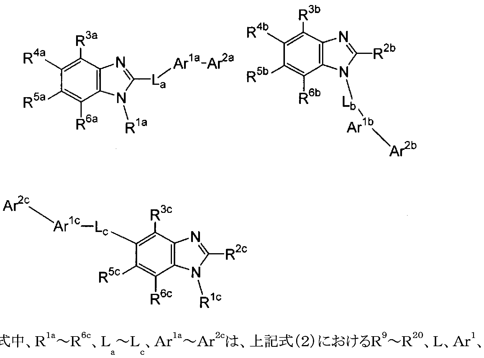
3.前記電子輸送性材料層の非錯体の含窒素複素環構造を含む化合物が、下記式 (1)で表される化合物である 1に記載の有機エレクト口ルミネッセンス素子。  3. The organic electroluminescent device according to 1, wherein the compound containing a non-complex nitrogen-containing heterocyclic structure of the electron transporting material layer is a compound represented by the following formula (1).
[化 1]  [Chemical 1]
Figure imgf000004_0001
(式中、!^〜 はそれぞれ、水素原子、置換もしくは無置換の核原子数 5〜60のァリ ール基、置換もしくは無置換の核原子数 5〜60のへテロアリール基、置換もしくは無 置換の炭素数 1〜50のアルキル基、置換もしくは無置換の炭素数 3〜50のシクロア ルキル基、置換もしくは無置換の核原子数 6〜50のァラルキル基、置換もしくは無置 換の炭素数 1〜50のアルコキシ基、置換もしくは無置換の核原子数 5〜50のァリー ルォキシ基、置換もしくは無置換の核原子数 5〜50のァリールチオ基、置換もしくは 無置換の炭素数 1〜50のアルコキシカルボニル基、置換もしくは無置換の核原子数 5〜50のァリール基で置換されたァミノ基、ハロゲン原子、シァノ基、ニトロ基、ヒドロ キシル基又はカルボキシル基であり、!^〜 の隣り合う置換基の一組が互いに結合 して芳香環又は複素環を形成していてもよい。 ) (Wherein ^^ is a hydrogen atom, a substituted or unsubstituted aryl group having 5 to 60 nuclear atoms, a substituted or unsubstituted heteroaryl group having 5 to 60 nuclear atoms, a substituted or unsubstituted group, respectively. Substituted alkyl group having 1 to 50 carbon atoms, substituted or unsubstituted cycloalkyl group having 3 to 50 carbon atoms, substituted or unsubstituted aralkyl group having 6 to 50 nuclear atoms, substituted or unsubstituted carbon number 1 ~ 50 alkoxy group, substituted or unsubstituted aryloxy group having 5 to 50 nuclear atoms, substituted or unsubstituted aryloxy group having 5 to 50 nuclear atoms, substituted or unsubstituted alkoxycarbonyl having 1 to 50 carbon atoms An amino group, a halogen atom, a cyano group, a nitro group, a hydroxyl group, or a carboxyl group, substituted with an aryl group having 5 to 50 nuclear atoms, substituted or unsubstituted, and adjacent to A pair is tied together And may form an aromatic ring or a heterocyclic ring.
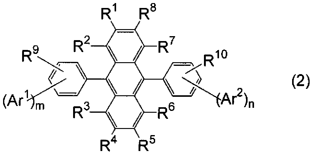
4.前記電子輸送性材料層の非錯体の含窒素複素環構造を含む化合物が、下記式 (2)で表される化合物である 1に記載の有機エレクト口ルミネッセンス素子。
Figure imgf000005_0001
4. The organic electroluminescent device according to 1, wherein the compound containing a non-complex nitrogen-containing heterocyclic structure of the electron transporting material layer is a compound represented by the following formula (2).
Figure imgf000005_0001
(式中、 R9〜R2°はそれぞれ、水素原子、置換もしくは無置換の核原子数 5〜60のァ リール基、置換もしくは無置換の核原子数 5〜60のへテロアリール基、置換もしくは 無置換の炭素数 1〜50のアルキル基、置換もしくは無置換の炭素数 3〜50のシクロ アルキル基、置換もしくは無置換の核原子数 6〜50のァラルキル基、置換もしくは無 置換の炭素数 1〜50のアルコキシ基、置換もしくは無置換の核原子数 5〜50のァリ ールォキシ基、置換もしくは無置換の核原子数 5〜50のァリールチオ基、置換もしく は無置換の炭素数 1〜50のアルコキシカルボニル基、置換もしくは無置換の核原子 数 5〜50のァリール基で置換されたァミノ基、ハロゲン原子、シァノ基、ニトロ基、ヒド 口キシル基又はカルボキシル基であり、 R9〜R2の隣り合う基が互いに結合して芳香 環を形成していてもよぐ R9〜R2の少なくとも 1つは下記式で示される置換基である (In the formula, R 9 to R 2 ° are each a hydrogen atom, a substituted or unsubstituted aryl group having 5 to 60 nuclear atoms, a substituted or unsubstituted heteroaryl group having 5 to 60 nuclear atoms, substituted or unsubstituted, An unsubstituted alkyl group having 1 to 50 carbon atoms, a substituted or unsubstituted cycloalkyl group having 3 to 50 carbon atoms, a substituted or unsubstituted aralkyl group having 6 to 50 nuclear atoms, a substituted or unsubstituted carbon number 1 ~ 50 alkoxy group, substituted or unsubstituted aryloxy group having 5 to 50 carbon atoms, substituted or unsubstituted aryloxy group having 5 to 50 nucleus atoms, substituted or unsubstituted carbon atoms 1 to 50 An alkoxycarbonyl group, an amino group substituted with a substituted or unsubstituted aryl group having 5 to 50 nuclear atoms, a halogen atom, a cyano group, a nitro group, a hydroxy group, or a carboxyl group, and R 9 to R 2 Adjacent groups of At least one of Yogu R 9 to R 2 also form an aromatic ring Te is a substituent represented by the following formula
[化 3] [Chemical 3]
L"~~- r1-Ar2 L "~~-r 1 - Ar 2
(Lは、置換もしくは無置換の炭素数 6〜60のァリーレン基、置換もしくは無置換の炭 素数 5〜60のへテロアリーレン基、又は置換もしくは無置換のフルォレニレン基であ り、 (L is a substituted or unsubstituted arylene group having 6 to 60 carbon atoms, a substituted or unsubstituted heteroarylene group having 5 to 60 carbon atoms, or a substituted or unsubstituted fluorenylene group,
Ar1は、置換もしくは無置換の炭素数 6〜60のァリーレン基、置換もしくは無置換の ピリジ-レン基又は置換もしくは無置換のキノリ-レン基であり、 Ar 1 is a substituted or unsubstituted arylene group having 6 to 60 carbon atoms, a substituted or unsubstituted pyridylene group, or a substituted or unsubstituted quinolylene group,
Ar2は、水素原子、置換もしくは無置換の核原子数 5〜60のァリール基、置換もしく は無置換のピリジル基、置換もしくは無置換のキノリル基、置換もしくは無置換の炭素 数 1〜50のアルキル基、置換もしくは無置換の炭素数 3〜50のシクロアルキル基、置 換もしくは無置換の核原子数 6〜50のァラルキル基、置換もしくは無置換の炭素数 1 〜50のアルコキシ基、置換もしくは無置換の核原子数 5〜50のァリールォキシ基、 置換もしくは無置換の核原子数 5〜50のァリールチオ基、置換もしくは無置換の炭 素数 1〜50のアルコキシカルボ-ル基、置換もしくは無置換の核原子数 5〜50のァ リール基で置換されたァミノ基、ハロゲン原子、シァノ基、ニトロ基、ヒドロキシル基又 はカルボキシル基である。 ) ) Ar 2 is a hydrogen atom, a substituted or unsubstituted aryl group having 5 to 60 nuclear atoms, a substituted or unsubstituted pyridyl group, a substituted or unsubstituted quinolyl group, a substituted or unsubstituted carbon number of 1 to 50. Alkyl group, substituted or unsubstituted cycloalkyl group having 3 to 50 carbon atoms, substituted or unsubstituted aralkyl group having 6 to 50 nuclear atoms, substituted or unsubstituted carbon number 1 ~ 50 alkoxy group, substituted or unsubstituted aryloxy group having 5 to 50 nuclear atoms, substituted or unsubstituted aryloxy group having 5 to 50 nuclear atoms, substituted or unsubstituted alkoxy carbo-carbon having 1 to 50 carbon atoms Or an amino group substituted with an aryl group having 5 to 50 substituted or unsubstituted aryl groups, a halogen atom, a cyano group, a nitro group, a hydroxyl group or a carboxyl group. ))
5.前記電子輸送性材料層の非錯体の含窒素複素環構造を含む化合物が、下記式 で表される化合物である 4に記載の有機エレクト口ルミネッセンス素子。  5. The organic electroluminescent device according to 4, wherein the compound containing a non-complex nitrogen-containing heterocyclic structure of the electron transporting material layer is a compound represented by the following formula:
[化 4]  [Chemical 4]
( Ar
Figure imgf000006_0001
(Ar
Figure imgf000006_0001
2とそれぞれ同じである。 Same as 2 .
6.前記ドナー層のドナーが、アルカリ金属、アルカリ土類金属、希土類金属、アル力 リ金属の酸化物、アルカリ金属のハロゲン化物、アルカリ土類金属の酸化物、アル力 リ土類金属のハロゲンィ匕物、希土類金属の酸化物、希土類金属のハロゲン化物、ァ ルカリ金属の有機錯体、アルカリ土類金属の有機錯体及び希土類金属の有機錯体 である 1〜5のいずれかに記載の有機エレクト口ルミネッセンス素子。  6. Donor of the donor layer is alkali metal, alkaline earth metal, rare earth metal, alkali metal oxide, alkali metal halide, alkaline earth metal oxide, alkaline earth metal halide Organic electroluminescence according to any one of 1 to 5, which is a porcelain, rare earth metal oxide, rare earth metal halide, alkali metal organic complex, alkaline earth metal organic complex, and rare earth metal organic complex element.
7.前記ァクセプター層のァクセプター力 電子吸引性の置換基又は電子欠乏環を 有する有機化合物である 1〜6のいずれかに記載の有機エレクト口ルミネッセンス素 子。 7. The acceptor force of the acceptor layer The organic electoluminescence element according to any one of 1 to 6, which is an organic compound having an electron-withdrawing substituent or an electron-deficient ring Child.
8.前記ァクセプター層のァクセプター力 キノイド誘導体、ァリールボラン誘導体、チ オビランジオキシド誘導体、ナフタルイミド誘導体又はへキサァザトリフエ-レン誘導 体である 7に記載の有機エレクト口ルミネッセンス素子。  8. The acceptor force of the acceptor layer 7. The organic electroluminescent device according to 7, wherein the acceptor layer is a quinoid derivative, an arylborane derivative, a thiobilan dioxide derivative, a naphthalimide derivative or a hexazatriphenylene derivative.
[0006] 本発明によれば、高効率で低電圧な複数の発光層を積層した有機 EL素子を提供 できる。 [0006] According to the present invention, it is possible to provide an organic EL device in which a plurality of light-emitting layers with high efficiency and low voltage are stacked.
図面の簡単な説明  Brief Description of Drawings
[0007] [図 1]本発明に係る有機 EL素子の第一の実施形態を示す図である。 FIG. 1 is a diagram showing a first embodiment of an organic EL device according to the present invention.
[図 2]図 1に示す有機 EL素子の中間接続層を示す図である。  2 is a view showing an intermediate connection layer of the organic EL element shown in FIG.
発明を実施するための最良の形態  BEST MODE FOR CARRYING OUT THE INVENTION
[0008] 本発明の有機 EL素子は、陽極と陰極の間に少なくとも 2つの有機発光層が介在し ており、有機発光層間に、少なくとも 1つの中間接続層を備えている。  [0008] The organic EL device of the present invention includes at least two organic light emitting layers interposed between an anode and a cathode, and includes at least one intermediate connection layer between the organic light emitting layers.
中間接続層は、陰極側から、ァクセプター層、ドナー層及び非錯体の含窒素複素 環構造を含む化合物を含む電子輸送材料層をこの順に積層してなる。  The intermediate connection layer is formed by laminating an acceptor layer, a donor layer, and an electron transport material layer containing a compound containing a non-complex nitrogen-containing heterocyclic structure in this order from the cathode side.
[0009] 図 1は、本発明の有機 EL素子の一実施形態を示す図である。この有機 EL素子は 、有機発光層を 3層積層した例である。  FIG. 1 is a view showing an embodiment of the organic EL device of the present invention. This organic EL device is an example in which three organic light emitting layers are laminated.
この有機 EL素子 1は、支持基板 10上に、透明陽極 20が設けられ、この透明陽極 2 0に、陰極 50が対向して設けられている。透明陽極 20と陰極 50の間には、第一の有 機発光層 30、第二の有機発光層 32、第三の有機発光層 34と、第一の中間接続層 4 0、第二の中間接続層 42が設けられている。ここで、第一の中間接続層 40が第一の 有機発光層 30と第二の有機発光層 32の間に、第二の中間接続層 42が第二の有機 発光層 32と第三の有機発光層 34の間に介在する。有機発光層 30, 32, 34が発す る光は、透明陽極 20を通して支持基板 10から取り出す。  In this organic EL element 1, a transparent anode 20 is provided on a support substrate 10, and a cathode 50 is provided opposite to the transparent anode 20. Between the transparent anode 20 and the cathode 50, the first organic light emitting layer 30, the second organic light emitting layer 32, the third organic light emitting layer 34, the first intermediate connection layer 40, and the second intermediate light emitting layer 34 are provided. A connection layer 42 is provided. Here, the first intermediate connection layer 40 is between the first organic light-emitting layer 30 and the second organic light-emitting layer 32, and the second intermediate connection layer 42 is the second organic light-emitting layer 32 and the third organic light-emitting layer 32. It is interposed between the light emitting layers 34. Light emitted from the organic light emitting layers 30, 32, and 34 is extracted from the support substrate 10 through the transparent anode 20.
[0010] 図 2は、本発明の中間接続層 40, 42を示す図である。図 2に示すように、中間接続 層 40, 42は、陰極 50側から、ァクセプター層 60、ドナー層 70及び非錯体の含窒素 複素環構造を含む化合物を含む電子輸送材料層 80をこの順に積層した構成をして いる。  FIG. 2 is a diagram showing the intermediate connection layers 40 and 42 of the present invention. As shown in FIG. 2, the intermediate connection layers 40 and 42 are formed by laminating an acceptor layer 60, a donor layer 70, and an electron transport material layer 80 containing a compound containing a non-complex nitrogen-containing heterocyclic structure in this order from the cathode 50 side. The configuration is as follows.
[0011] 本発明において、ァクセプター層 60とは、隣接する有機発光層から電子を引き抜き (電子をアクセプトする)、ドナー層へ移送する層である。また、ドナー層 70とは、ァク セプター層から電子を受け取り電子を電子輸送材料層に注入する(電子をドナーす る)層である。電子輸送材料層 80は、隣接する有機発光層に電子を注入する層であ る。 In the present invention, the acceptor layer 60 refers to extracting electrons from an adjacent organic light emitting layer. A layer that accepts electrons and transports it to the donor layer. The donor layer 70 is a layer that receives electrons from the acceptor layer and injects electrons into the electron transport material layer (donates electrons). The electron transport material layer 80 is a layer that injects electrons into the adjacent organic light emitting layer.
[0012] この素子 1の第一の有機発光層 30においては、陽極 20から正孔が注入され、第一 の中間接続層 40の電子輸送材料層から電子が注入されることにより発光する。第一 の中間接続層 40の電子輸送材料層には、ァクセプター層からドナー層を通して電子 が移送される。  In the first organic light emitting layer 30 of the element 1, light is emitted by injecting holes from the anode 20 and injecting electrons from the electron transport material layer of the first intermediate connection layer 40. Electrons are transferred from the acceptor layer to the electron transport material layer of the first intermediate connection layer 40 through the donor layer.
[0013] 第二の有機発光層 32においては、第一の中間接続層 40のァクセプター層から正 孔が注入され、第二の中間接続層 42の電子輸送材料層カゝら電子が注入されること により発光する。第一の中間接続層 40の電子輸送材料層 80には、ァクセプター層 力もドナー層を通して電子が移送される。第二の中間接続層 42の電子輸送材料層 には、ァクセプター層からドナー層を通して電子が移送される。  In the second organic light emitting layer 32, holes are injected from the acceptor layer of the first intermediate connection layer 40, and electrons are injected from the electron transport material layer of the second intermediate connection layer 42. It emits light. Electrons are transferred to the electron transport material layer 80 of the first intermediate connection layer 40 through the donor layer as well as the acceptor layer force. Electrons are transferred from the acceptor layer to the electron transport material layer of the second intermediate connection layer 42 through the donor layer.
[0014] 第三の有機発光層 34においては、陰極 50から電子が注入され、第二の中間接続 層 42のァクセプター層力も正孔が注入されることにより発光する。第二の中間接続層 42の電子輸送材料層 80には、ァクセプター層からドナー層を通して電子が移送され る。  [0014] In the third organic light emitting layer 34, electrons are injected from the cathode 50, and the acceptor layer force of the second intermediate connection layer 42 also emits light by injecting holes. Electrons are transferred from the acceptor layer to the electron transport material layer 80 of the second intermediate connection layer 42 through the donor layer.
[0015] 本発明は、中間接続層に特定の電子輸送材料層を用いることによって、低電圧化 することができる。このため、有機発光層を積層した有機 EL素子は高電圧化しやす いが、このような積層型の有機 EL素子であっても、低電圧化、高効率化が図られる。  [0015] The present invention can reduce the voltage by using a specific electron transport material layer for the intermediate connection layer. For this reason, an organic EL element in which organic light emitting layers are stacked is easy to increase the voltage, but even such a stacked organic EL element can achieve a lower voltage and higher efficiency.
[0016] 尚、本実施形態において、 3層の有機発光層 30, 32, 34、 2層の中間接続層 40, 42は、それぞれ異なっていても、同一でもよい。  In the present embodiment, the three organic light emitting layers 30, 32, 34 and the two intermediate connection layers 40, 42 may be different or the same.
[0017] この実施形態では、有機発光層は 3層積層されているが、 2層又は 4層以上積層し てもよい。さらに、この実施形態では、中間接続層が各有機発光層の間にある力 少 なくとも二つの有機発光層の間に図 2に示す積層構造の中間接続層が一つあれば よい。従って、その他の有機発光層がある場合は、異なる有機発光層が直接接して Vヽてもよ ヽし、図 2に示す積層構造ではな 、通常の中間接続層が介在してもよ!/ヽ。  In this embodiment, three organic light emitting layers are laminated, but two or four or more layers may be laminated. Further, in this embodiment, it is sufficient that there is at least one intermediate connection layer having the laminated structure shown in FIG. 2 between the two organic light emitting layers. Therefore, when there are other organic light-emitting layers, different organic light-emitting layers may be in direct contact with each other and V may be used, or a normal intermediate connection layer may be interposed instead of the laminated structure shown in FIG.ヽ.
[0018] また、この実施形態では、透明電極は陽極である力 陰極でも構わない。さらに、本 発明の有機 EL素子はトップェミッションタイプでもボトムェミッションタイプでもよい。 Vヽずれのタイプでも、光を取り出す側の電極が光透過性となる。 In this embodiment, the transparent electrode may be a power cathode that is an anode. In addition, book The organic EL element of the invention may be a top emission type or a bottom emission type. Even in the case of the V-shift type, the electrode from which light is extracted becomes light transmissive.
[0019] 以下、本発明の有機 EL素子の各構成部材について説明する。 Hereinafter, each component of the organic EL element of the present invention will be described.
1.支持基板  1.Support substrate
支持基板は、有機 EL素子を支持するための部材であり、そのため機械的強度や、 寸法安定性に優れていることが好ましい。このような基板としては、具体的には、ガラ ス板、金属板、セラミックス板、又はプラスチック板 (ポリカーボネート榭脂、アクリル榭 脂、塩化ビニル榭脂、ポリエチレンテレフタレート榭脂、ポリイミド榭脂、ポリエステノレ 榭脂、エポキシ榭脂、フエノール榭脂、シリコン榭脂、フッ素榭脂等)等を挙げることが できる。  The support substrate is a member for supporting the organic EL element, and therefore it is preferable that the support substrate is excellent in mechanical strength and dimensional stability. Specific examples of such a substrate include a glass plate, a metal plate, a ceramic plate, or a plastic plate (polycarbonate resin, acrylic resin, vinyl chloride resin, polyethylene terephthalate resin, polyimide resin, polyester resin. Resin, epoxy resin, phenol resin, silicon resin, fluorine resin, etc.).
[0020] これらの材料からなる基板は、有機 EL表示装置内への水分の侵入を避けるために 、さらに無機膜を形成したり、フッ素榭脂を塗布したりして、防湿処理や疎水性処理を 施してあることが好ましい。特に、有機発光媒体への水分の侵入を避けるために、基 板における含水率及びガス透過係数を小さくすることが好ましい。具体的に、支持基 板の含水率を 0. 0001重量%以下及びガス透過係数を 1 X 10"13cc - cm/cm2 - Se c. cmHg以下とすることがそれぞれ好ましい。 [0020] In order to avoid moisture intrusion into the organic EL display device, the substrate made of these materials is further formed with an inorganic film or coated with fluorine resin to prevent moisture or hydrophobic treatment. Is preferably applied. In particular, it is preferable to reduce the moisture content and gas permeability coefficient of the substrate in order to avoid moisture intrusion into the organic light emitting medium. Specifically, it is preferable that the moisture content of the support substrate is 0.0001 wt% or less and the gas permeability coefficient is 1 × 10 ” 13 cc-cm / cm 2 -Sec. CmHg or less.
支持基板側力も光を取出す場合は、支持基板は可視光に対する透過率が 50%以 上の透明であることが望ましいが、その反対側力も EL発光を取り出す場合には、基 板は必ずしも透明性を有する必要はな 、。  If the supporting substrate side force also extracts light, it is desirable that the supporting substrate is transparent with a visible light transmittance of 50% or more, but if the opposite side force also extracts EL light emission, the substrate is not necessarily transparent. There is no need to have.
[0021] 2.陽極  [0021] 2. Anode
陽極は、仕事関数の大きい (例えば、 4. OeV以上)金属、合金、電気電導性化合 物又はこれらの混合物を使用することが好ましい。具体的には、酸化インジウム錫合 金 (ITO)、インジウム—亜鉛酸ィ匕物(IZO)インジウム銅、スズ、酸化亜鉛、金、白金、 ノラジウム等の 1種を単独で、又は 2種以上を組み合わせて使用することができる。  As the anode, it is preferable to use a metal, an alloy, an electrically conductive compound, or a mixture thereof having a high work function (for example, 4. OeV or more). Specifically, indium tin oxide (ITO), indium-zinc oxide (IZO) indium copper, tin, zinc oxide, gold, platinum, noradium, etc., alone or in combination of two or more Can be used in combination.
[0022] 陽極は、これらの電極物質を蒸着法やスパッタリング法等の方法で薄膜を形成させ ることにより作製することができる。また、陽極の厚さは、特に制限されるものではない 1S 好ましくは 10〜1000nmであり、より好ましくは 10〜200nmである。さらに、陽極 から有機発光媒体層から放射された光を外部に取り出す場合は、好ましくは実質的 に透明、即ち、光透過率が 50%以上である。 [0022] The anode can be produced by forming a thin film of these electrode materials by a method such as vapor deposition or sputtering. Further, the thickness of the anode is not particularly limited. 1S is preferably 10 to 1000 nm, and more preferably 10 to 200 nm. Further, when taking out the light emitted from the organic light emitting medium layer from the anode to the outside, it is preferable that Is transparent, that is, the light transmittance is 50% or more.
[0023] 3.陰極 [0023] 3. Cathode
陰極は、好ましくは仕事関数の小さい(例えば、 4. OeV未満)金属、合金、電気電 導性化合物又はこれらの混合物を使用する。具体的には、マグネシウム、アルミ-ゥ ム、インジウム、リチウム、ナトリウム、セシウム、銀等の 1種を単独で、又は 2種以上を 組み合わせて使用することができる。また陰極の厚さは、特に制限されるものではな いが、好ましくは 10〜1000nmであり、より好ましくは 10〜200nmである。  The cathode preferably uses a metal, an alloy, an electrically conductive compound or a mixture thereof having a low work function (eg, less than 4. OeV). Specifically, one of magnesium, aluminum, indium, lithium, sodium, cesium, silver and the like can be used alone or in combination of two or more. The thickness of the cathode is not particularly limited, but is preferably 10 to 1000 nm, more preferably 10 to 200 nm.
[0024] 4.有機発光層 [0024] 4. Organic light emitting layer
有機発光層は、電子と正孔とが再結合して、 EL発光が可能な有機発光媒体層を 含む。かかる有機発光層は、例えば、以下の各層を積層して構成することができる。 The organic light emitting layer includes an organic light emitting medium layer capable of EL emission by recombination of electrons and holes. Such an organic light emitting layer can be constituted by laminating the following layers, for example.
(i) 有機発光媒体層 (i) Organic light emitting medium layer
(ii) 正孔注入層 Z有機発光媒体層  (ii) Hole injection layer Z Organic light emitting medium layer
(iii) 有機発光媒体層 Z電子注入層  (iii) Organic light emitting medium layer Z electron injection layer
(iv) 正孔注入層 Z有機発光媒体層 Z電子注入'輸送層  (iv) Hole injection layer Z Organic light emitting medium layer Z Electron injection 'transport layer
(V) 正孔注入層 Z有機発光媒体層 Z付着改善層  (V) Hole injection layer Z Organic light emitting medium layer Z adhesion improving layer
これらの中で、(iv)の構成が、より高い発光輝度が得られ、耐久性にも優れているこ とから、通常、好ましく用いられる。  Among these, the configuration (iv) is usually preferably used because it can provide higher emission luminance and is excellent in durability.
[0025] 有機 EL素子の発光媒体層は以下(1)〜(3)の機能を併せ持つものである。 [0025] The light emitting medium layer of the organic EL element has the following functions (1) to (3).
(1) 注入機能;電界印加時に陽極又は正孔注入層より正孔を注入することができ、 陰極又は電子注入層より電子を注入することができる機能  (1) Injection function: Function that can inject holes from the anode or hole injection layer when an electric field is applied, and can inject electrons from the cathode or electron injection layer
(2) 輸送機能;注入した電荷 (電子と正孔)を電界の力で移動させる機能  (2) Transport function: Function to move injected charges (electrons and holes) by the force of electric field
(3) 発光機能;電子と正孔の再結合の場を提供し、これを発光につなげる機能 ただし、正孔の注入されやすさと電子の注入されやすさに違いがあってもよぐまた (3) Luminescent function; a function that provides a field for recombination of electrons and holes and connects this to light emission.However, there is no difference between the ease of hole injection and the ease of electron injection.
、正孔と電子の移動度で表される輸送能に大小があってもよいが、どちらか一方の電 荷を移動することが好まし 、。 The transport capacity expressed by the mobility of holes and electrons may be large or small, but it is preferable to move one of the charges.
[0026] この発光媒体層を形成する方法としては、例えば蒸着法、スピンコート法、 LB法等 の公知の方法を適用することができる。発光媒体層は、特に分子堆積膜であることが 好ましい。ここで分子堆積膜とは、気相状態の材料化合物から沈着され形成された 薄膜や、溶液状態又は液相状態の材料化合物から固体化され形成された膜のこと であり、通常この分子堆積膜は、 LB法により形成された薄膜 (分子累積膜)とは凝集 構造、高次構造の相違や、それに起因する機能的な相違により区分することができる また、特開昭 57— 51781号公報に開示されているように、榭脂等の結着剤と材料 化合物とを溶剤に溶力して溶液とした後、これをスピンコート法等により薄膜ィ匕するこ とによっても、発光媒体層を形成することができる。 [0026] As a method for forming the luminescent medium layer, for example, a known method such as a vapor deposition method, a spin coating method, or an LB method can be applied. The luminescent medium layer is particularly preferably a molecular deposited film. Here, the molecular deposition film is formed by deposition from a material compound in a gas phase state. This is a thin film or a film formed by solidification from a material compound in a solution state or a liquid phase state. Usually, this molecular deposited film has a cohesive structure and high structure from a thin film (molecular accumulated film) formed by the LB method. It can be classified by the difference in the next structure and the functional difference resulting from it. Also, as disclosed in JP-A-57-51781, a binder such as rosin and a material compound are mixed with a solvent. The light emitting medium layer can also be formed by forming a solution by dissolving the solution in a thin film and then thinly forming the solution by a spin coating method or the like.
[0027] [有機発光媒体層]  [0027] [Organic luminescent medium layer]
有機発光媒体層に使用できる発光材料又はドーピング材料としては、例えば、ァリ ールァミン化合物及び Z又はスチリルアミン化合物、アントラセン、ナフタレン、フエナ ントレン、ピレン、テトラセン、コロネン、タリセン、フルォレセイン、ペリレン、フタ口ペリ レン、ナフタ口ペリレン、ペリノン、フタ口ペリノン、ナフタ口ペリノン、ジフエニルブタジ ェン、テトラフエ-ルブタジエン、クマリン、ォキサジァゾール、アルダジン、ビスべンゾ キサゾリン、ビススチリル、ピラジン、シクロペンタジェン、キノリン金属錯体、ァミノキノ リン金属錯体、ベンゾキノリン金属錯体、ィミン、ジフエ-ルエチレン、ビ-ルアントラ セン、ジァミノカルバゾール、ピラン、チォピラン、ポリメチン、メロシアニン、イミダゾー ルキレートィ匕ォキシノイド化合物、キナクリドン、ルブレン及び蛍光色素等が挙げられ るが、これらに限定されるものではない。  Examples of the light emitting material or doping material that can be used for the organic light emitting medium layer include arylamine compounds and Z or styrylamine compounds, anthracene, naphthalene, phenanthrene, pyrene, tetracene, coronene, taricene, fluorescein, perylene, and lid-periphery. Lene, Naphtha-perylene, Perinone, Lid-perinone, Naphtal-perinone, Diphenylbutadiene, Tetraphenylbutadiene, Coumarin, Oxadiazole, Ardazine, Bisbenzoxazoline, Bisstyryl, Pyrazine, Cyclopentagen, Quinoline metal complex, Aminoquino Phosphorus metal complex, benzoquinoline metal complex, imine, diphenylethylene, berylanthracene, diaminocarbazole, pyran, thiopyran, polymethine, merocyanine, imidazole chelate Examples thereof include, but are not limited to, oxinoid compounds, quinacridone, rubrene, and fluorescent dyes.
[0028] また、本発明の有機 EL素子は、有機発光媒体層が、ァリールアミンィ匕合物及び Z 又はスチリルアミンィ匕合物を含有すると好ま U、。  [0028] In the organic EL device of the present invention, the organic light emitting medium layer preferably contains an arylamine compound and Z or a styrylamine compound.
ァリールアミンィ匕合物としては下記式 (A)で表される化合物等が挙げられ、スチリル ァミン化合物としては下記式 (B)で表される化合物等が挙げられる。  Examples of the arylamine compounds include compounds represented by the following formula (A), and examples of the styrylamine compounds include compounds represented by the following formula (B).
[0029] [化 5] [0029] [Chemical 5]
Figure imgf000012_0001
(式中、 Ar は、フエ-ル、ビフエ-ル、テルフエ-ル、スチルベン又はジスチリルァリ ールであり、 Ar3 2及び Ar3 3は、それぞれ水素原子又は置換もしくは無置換の炭素 数が 6〜20の芳香族基である。 p'は、 1〜4の整数である。さらに好ましくは Ar3 2及 び Z又は Ar3 はスチリル基が置換されている。 ) (In the formula, Ar is phenyl, biphenyl, terpheal, stilbene or distyryl aryl, and Ar 3 2 and Ar 3 3 are each a hydrogen atom or a substituted or unsubstituted carbon number of 6 to 6. 20 is an aromatic group, and p ′ is an integer of 1 to 4. More preferably, Ar 3 2 and Z or Ar 3 are substituted with a styryl group.
ここで、炭素数が 6〜20の芳香族基としては、フエニル基、ナフチル基、アントラセ -ル基、フエナントリル基、テルフエ-ル基等が好ましい。  Here, the aromatic group having 6 to 20 carbon atoms is preferably a phenyl group, a naphthyl group, an anthracyl group, a phenanthryl group, a terphenyl group, or the like.
[化 6] [Chemical 6]
Figure imgf000012_0002
(式中、 Ar3M〜Ar3G6は、置換もしくは無置換の核炭素数 5〜40のァリール基である 。 q,は、 1〜4の整数である。 ) (Wherein, Ar 3M to Ar 3G6 is a substituted or unsubstituted Ariru group having a carbon number of 5 to 40. Q, is an integer from 1 to 4.)
ここで、核原子数が 5〜40のァリール基としては、フエニル、ナフチル、アントラセ- ル、フエナントリル、ピレニル、クリセニル、コロニノレ、ビフエニル、テルフエニル、ピロ一 リル、フラニル、チォフエニル、ベンゾチォフエニル、ォキサジァゾリル、ジフエニルァ ントラセニル、インドリル、カルバゾリル、ピリジル、ベンゾキノリル、フルオランテニル、 ァセナフトフルオランテュル、スチルベン等が好ましい。核原子数が 5〜40のァリー ル基は、さらに置換基により置換されていてもよぐ好ましい置換基としては、炭素数 1〜6のアルキル基(ェチル基、メチル基、イソプロピル基、 n—プロピル基、 s—ブチ ル基、 t ブチル基、ペンチル基、へキシル基、シクロペンチル基、シクロへキシル基 等)、炭素数 1〜6のアルコキシ基 (エトキシ基、メトキシ基、イソプロポキシ基、 n—プ 口ポキシ基、 s ブトキシ基、 t ブトキシ基、ペントキシ基、へキシルォキシ基、シクロ ペントキシ基、シクロへキシルォキシ基等)、核原子数 5〜40のァリール基、核原子数 5〜40のァリール基で置換されたァミノ基、核原子数 5〜40のァリール基を有するェ ステル基、炭素数 1〜6のアルキル基を有するエステル基、シァノ基、ニトロ基、ハロ ゲン原子 (塩素、臭素、ヨウ素等)が挙げられる。 Here, aryl groups having 5 to 40 nuclear atoms include phenyl, naphthyl, anthracyl, phenanthryl, pyrenyl, chrysenyl, coroninole, biphenyl, terphenyl, pyrrolyl, furanyl, thiophenyl, benzothiophenyl, oxadiazolyl. Diphenylanthracenyl, indolyl, carbazolyl, pyridyl, benzoquinolyl, fluoranthenyl, acenaphthofluoranthur, stilbene and the like are preferable. The aryl group having 5 to 40 nuclear atoms may be further substituted with a substituent. Examples of the preferred substituent include alkyl groups having 1 to 6 carbon atoms (ethyl group, methyl group, isopropyl group, n- Propyl group, s-butyl Group, t-butyl group, pentyl group, hexyl group, cyclopentyl group, cyclohexyl group, etc.), alkoxy group having 1 to 6 carbon atoms (ethoxy group, methoxy group, isopropoxy group, n-portoxy group, s butoxy group, t butoxy group, pentoxy group, hexyloxy group, cyclopentoxy group, cyclohexyloxy group, etc.), aryl group having 5 to 40 nuclear atoms, amino group substituted with aryl group having 5 to 40 nuclear atoms Groups, ester groups having an aryl group having 5 to 40 nuclear atoms, ester groups having an alkyl group having 1 to 6 carbon atoms, cyan groups, nitro groups, halogen atoms (chlorine, bromine, iodine, etc.). .
発光媒体層に使用できるホスト材料としては、下記(1)〜(10)で表される化合物が 好ましい。  As the host material that can be used in the light emitting medium layer, compounds represented by the following (1) to (10) are preferable.
下記式(1)で表されるアントラセン誘導体。  An anthracene derivative represented by the following formula (1).
[化 7]  [Chemical 7]
Figure imgf000013_0001
(式中、 Ar、 Ar'はそれぞれ置換もしくは無置換の核原子数 5〜60のァリール基又は 置換もしくは無置換の核原子数 5〜60のへテロアリール基である。 (In the formula, Ar and Ar ′ are each a substituted or unsubstituted aryl group having 5 to 60 nucleus atoms or a substituted or unsubstituted heteroaryl group having 5 to 60 nucleus atoms.
Xは、それぞれ置換もしくは無置換の核炭素数 6〜50のァリール基、置換もしくは 無置換の核原子数 5〜50のへテロアリール基、置換もしくは無置換の炭素数 1〜50 のアルキル基、置換もしくは無置換の炭素数 1〜50のアルコキシ基、置換もしくは無 置換の炭素数 6〜50のァラルキル基、置換もしくは無置換の核原子数 5〜50のァリ ールォキシ基、置換もしくは無置換の核原子数 5〜50のァリールチオ基、置換もしく は無置換の炭素数 1〜50のアルコキシカルボ-ル基、カルボキシル基、ハロゲン原 子、シァノ基、ニトロ基又はヒドロキシル基である。  X is substituted or unsubstituted aryl group having 6 to 50 nuclear carbon atoms, substituted or unsubstituted heteroaryl group having 5 to 50 nuclear atoms, substituted or unsubstituted alkyl group having 1 to 50 carbon atoms, substituted Or an unsubstituted alkoxy group having 1 to 50 carbon atoms, a substituted or unsubstituted aralkyl group having 6 to 50 carbon atoms, a substituted or unsubstituted aryloxy group having 5 to 50 nucleus atoms, a substituted or unsubstituted nucleus. It is a 5-50 atom arylthio group, a substituted or unsubstituted alkoxycarbon group having 1-50 carbon atoms, a carboxyl group, a halogen atom, a cyano group, a nitro group or a hydroxyl group.
a及び bは、それぞれ 0〜4の整数である。  a and b are each an integer of 0 to 4.
nは 1〜3の整数である。 ) [0033] 下記式(2)で表されるアントラセン誘導体。 n is an integer of 1 to 3. ) [0033] An anthracene derivative represented by the following formula (2).
[化 8]  [Chemical 8]
Figure imgf000014_0001
(式中、 Ar1及び Ar2は、それぞれ置換もしくは無置換の核炭素数 6〜50のァリール 基、又は置換もしくは無置換の核原子数 5〜60のへテロアリール基である。 (In the formula, Ar 1 and Ar 2 are each a substituted or unsubstituted aryl group having 6 to 50 nuclear carbon atoms or a substituted or unsubstituted heteroaryl group having 5 to 60 nuclear atoms.
m及び nは、それぞれ 1〜4の整数である。  m and n are each an integer of 1 to 4.
R^R10^,それぞれ水素原子、置換もしくは無置換の核炭素数 6〜50のァリール 基、置換もしくは無置換の核原子数 5〜50のへテロアリール基、置換もしくは無置換 の炭素数 1〜50のアルキル基、置換もしくは無置換のシクロアルキル基、置換もしく は無置換の炭素数 1〜50のアルコキシ基、置換もしくは無置換の炭素数 6〜50のァ ラルキル基、置換もしくは無置換の核原子数 5〜50のァリールォキシ基、置換もしく は無置換の核原子数 5〜50のァリールチオ基、置換もしくは無置換の炭素数 1〜50 のアルコキシカルボ-ル基、置換もしくは無置換のシリル基、カルボキシル基、ハロゲ ン原子、シァノ基、ニトロ基又はヒドロキシル基である。 ) R ^ R 10 ^, each hydrogen atom, substituted or unsubstituted aryl group having 6 to 50 nuclear carbon atoms, substituted or unsubstituted heteroaryl group having 5 to 50 nuclear atoms, substituted or unsubstituted carbon atoms 1 to 50 alkyl groups, substituted or unsubstituted cycloalkyl groups, substituted or unsubstituted alkoxy groups having 1 to 50 carbon atoms, substituted or unsubstituted aralkyl groups having 6 to 50 carbon atoms, substituted or unsubstituted Aryloxy group having 5 to 50 nucleus atoms, substituted or unsubstituted aryloxy group having 5 to 50 nucleus atoms, substituted or unsubstituted alkoxycarbonyl group having 1 to 50 carbon atoms, substituted or unsubstituted silyl group Group, carboxyl group, halogen atom, cyano group, nitro group or hydroxyl group. )
[0034] 下記式(3)で表されるアントラセン誘導体。 [0034] An anthracene derivative represented by the following formula (3).
[化 9] [Chemical 9]
Figure imgf000015_0001
Y  Y
(3)  (3)
(式中、 Α1及び Α2は、それぞれ置換もしくは無置換の核炭素数 10〜20の縮合芳香 族環基である。 (Wherein Α 1 and Α 2 are each a substituted or unsubstituted condensed aromatic ring group having 10 to 20 nuclear carbon atoms.
Ar3及び Ar4は、それぞれ水素原子又は置換もしくは無置換の核炭素数 6〜50の ァリール基である。 Ar 3 and Ar 4 are each a hydrogen atom or a substituted or unsubstituted aryl group having 6 to 50 nuclear carbon atoms.
R^R10^,それぞれ水素原子、置換もしくは無置換の核炭素数 6〜50のァリール 基、置換もしくは無置換の核原子数 5〜50のへテロアリール基、置換もしくは無置換 の炭素数 1〜50のアルキル基、置換もしくは無置換のシクロアルキル基、置換もしく は無置換の炭素数 1〜50のアルコキシ基、置換もしくは無置換の炭素数 6〜50のァ ラルキル基、置換もしくは無置換の核原子数 5〜50のァリールォキシ基、置換もしく は無置換の核原子数 5〜50のァリールチオ基、置換もしくは無置換の炭素数 1〜50 のアルコキシカルボ-ル基、置換もしくは無置換のシリル基、カルボキシル基、ハロゲ ン原子、シァノ基、ニトロ基又はヒドロキシル基である。 R ^ R 10 ^, each hydrogen atom, substituted or unsubstituted aryl group having 6 to 50 nuclear carbon atoms, substituted or unsubstituted heteroaryl group having 5 to 50 nuclear atoms, substituted or unsubstituted carbon atoms 1 to 50 alkyl groups, substituted or unsubstituted cycloalkyl groups, substituted or unsubstituted alkoxy groups having 1 to 50 carbon atoms, substituted or unsubstituted aralkyl groups having 6 to 50 carbon atoms, substituted or unsubstituted Aryloxy group having 5 to 50 nucleus atoms, substituted or unsubstituted aryloxy group having 5 to 50 nucleus atoms, substituted or unsubstituted alkoxycarbonyl group having 1 to 50 carbon atoms, substituted or unsubstituted silyl group Group, carboxyl group, halogen atom, cyano group, nitro group or hydroxyl group.
Ar3、 Ar4、 R9及び R1。は、それぞれ複数であってもよぐ隣接するもの同士で飽和も しくは不飽和の環状構造を形成していてもよい。 ) Ar 3 , Ar 4 , R 9 and R 1 . May be a plurality or adjacent ones may form a saturated or unsaturated cyclic structure. )
下記式 (4)で表されるアントラセン誘導体。  An anthracene derivative represented by the following formula (4).
[化 10] [Chemical 10]
Figure imgf000016_0001
(式中、 1^〜 °は、それぞれ水素原子、アルキル基,シクロアルキル基,置換もしく は無置換のァリール基,アルコキシル基,ァリーロキシ基,アルキルアミノ基,ァルケ -ル基,ァリールアミノ基又は置換もしくは無置換の複素環式基を示す。 (In the formula, 1 ^ to ° are each a hydrogen atom, an alkyl group, a cycloalkyl group, a substituted or unsubstituted aryl group, an alkoxyl group, an aryloxy group, an alkylamino group, an alkyl group, an aryl group, or a substituted group. Or an unsubstituted heterocyclic group is shown.
a及び bは、それぞれ 1〜5の整数を示し、それらが 2以上の場合、 R11同士又は R12 同士は、同一でも異なっていてもよぐまた R11同士又は R12同士が結合して環を形成 していてもよいし、 R13と R14, R15と R16, R17と R18, R19と R2が互いに結合して環を形 成していてもよい。 a and b each represent an integer of 1 to 5, and when they are 2 or more, R 11 or R 12 may be the same or different, and R 11 or R 12 are bonded to each other. A ring may be formed, or R 13 and R 14 , R 15 and R 16 , R 17 and R 18 , R 19 and R 2 may be bonded to each other to form a ring.
L1は単結合、 -0- , -S- , N (R)—(Rはアルキル基又は置換もしくは無置換 のァリール基である)、アルキレン基又はァリーレン基を示す。 ) L 1 represents a single bond, -0-, -S-, N (R) — (where R is an alkyl group or a substituted or unsubstituted aryl group), an alkylene group or an arylene group. )
下記式(5)で表されるアントラセン誘導体。  An anthracene derivative represented by the following formula (5).
[化 11] [Chemical 11]
Figure imgf000016_0002
(式中、 R 〜RdUは、それぞれ水素原子、アルキル基,シクロアルキル基,ァリール基 ,アルコキシル基,ァリーロキシ基,アルキルアミノ基,ァリールアミノ基又は置換もしく は無置換の複数環基を示す。 (Wherein R to R dU are a hydrogen atom, an alkyl group, a cycloalkyl group, and an aryl group, respectively. Represents an alkoxyl group, an aryloxy group, an alkylamino group, an arylamino group, or a substituted or unsubstituted multiple ring group.
C d, e及び fは、それぞれ 1〜5の整数を示し、それらが 2以上の場合、 R21同士, R 22同士, R26同士又は R27同士は、同一でも異なっていてもよぐまた R21同士, R22同 士, R26同士又は R27同士が結合して環を形成していてもよいし、 R23と R24, R28と R29 が互 、に結合して環を形成して 、てもよ 、。 C d, e and f each represent an integer of 1 to 5, and when they are 2 or more, R 21 , R 2 2 , R 26, or R 27 may be the same or different. Further, R 21 , R 22 , R 26 or R 27 may be bonded to form a ring, or R 23 and R 24 , R 28 and R 29 may be bonded to each other to form a ring. You can form,
L2は単結合、 -0- , -S- , — N (R)— (Rはアルキル基又は置換もしくは無置換 のァリール基である)、アルキレン基又はァリーレン基を示す。 ) L 2 represents a single bond, -0-, -S-, —N (R) — (R is an alkyl group or a substituted or unsubstituted aryl group), an alkylene group or an arylene group. )
[0037] 下記式 (6)で表されるアントラセン誘導体。 [0037] An anthracene derivative represented by the following formula (6):
[化 12]  [Chemical 12]
(A 3 ) e— (X 1 ) f - (A r 5 ) g - (Y 1 ) h— ( B 1) ; ( 6 ) (A 3 ) e — (X 1 ) f- (A r 5 ) g- (Y 1 ) h — (B 1 ); (6)
(式中、 X1は、それぞれ置換もしくは無置換のピレン残基である。 (In the formula, each X 1 is a substituted or unsubstituted pyrene residue.
A3及び B1は、それぞれ水素原子、置換もしくは無置換の核炭素数 3〜50の芳香族 炭化水素基、置換もしくは無置換の核炭素数 1〜50の芳香族複素環基、置換もしく は無置換の炭素数 1〜50のアルキル基あるいはアルキレン基、又は置換もしくは無 置換の炭素数 1〜50のァルケ-ル基あるいはァルケ-レン基である。 A 3 and B 1 are each a hydrogen atom, a substituted or unsubstituted aromatic hydrocarbon group having 3 to 50 nuclear carbon atoms, a substituted or unsubstituted aromatic heterocyclic group having 1 to 50 nuclear carbon atoms, substituted or unsubstituted Is an unsubstituted alkyl group or alkylene group having 1 to 50 carbon atoms, or a substituted or unsubstituted alkyl group or alkylene group having 1 to 50 carbon atoms.
Ar5は、それぞれ置換もしくは無置換の核炭素数 3〜50の芳香族炭化水素基又は 置換もしくは無置換の核炭素数 1〜50の芳香族複素環基である。 Ar 5 is a substituted or unsubstituted aromatic hydrocarbon group having 3 to 50 nuclear carbon atoms or a substituted or unsubstituted aromatic heterocyclic group having 1 to 50 nuclear carbon atoms, respectively.
Y1は、それぞれ置換もしくは無置換のァリール基である。 Y 1 is each a substituted or unsubstituted aryl group.
fは 1〜3の整数、 e及び iはそれぞれ 0〜4の整数、 hは 0〜3の整数、 gは 1〜5の整 数である。 )  f is an integer from 1 to 3, e and i are each an integer from 0 to 4, h is an integer from 0 to 3, and g is an integer from 1 to 5. )
[0038] 下記式(7)で表されるアントラセン誘導体。  [0038] An anthracene derivative represented by the following formula (7):
[化 13] [Chemical 13]
Figure imgf000018_0001
(式中、 Ar6及び Ar7は、それぞれ置換もしくは無置換の核炭素数 6〜50のァリール 基である。 (In the formula, Ar 6 and Ar 7 are each a substituted or unsubstituted aryl group having 6 to 50 nuclear carbon atoms.
L3及び L4は、それぞれ置換もしくは無置換のフエ-レン基、置換もしくは無置換の ナフタレ-レン基、置換もしくは無置換のフルォレニレン基又は置換もしくは無置換 のジベンゾシロリレン基である。 L 3 and L 4 are each a substituted or unsubstituted phenylene group, a substituted or unsubstituted naphthalene group, a substituted or unsubstituted fluorenylene group, or a substituted or unsubstituted dibenzosilolylene group.
mは 0〜2の整数、 nは 1〜4の整数、 sは 0〜2の整数、 tは 0〜4の整数である。 また、 L3又は Ar6は、ピレンの 1〜5位のいずれかに結合し、 L4又は Ar7は、ピレンのm is an integer from 0 to 2, n is an integer from 1 to 4, s is an integer from 0 to 2, and t is an integer from 0 to 4. L 3 or Ar 6 is bonded to any one of positions 1 to 5 of pyrene, and L 4 or Ar 7 is bonded to pyrene.
6〜10位のいずれかに結合する。 ) It binds to any of the 6-10 positions. )
下記式(8)で表されるスピオ口フルオレン誘導体。  A spio-mouth fluorene derivative represented by the following formula (8).
[化 14]  [Chemical 14]
Figure imgf000018_0002
(式中、 A4〜A 'は、それぞれ置換もしくは無置換のビフエ-ル基又は置換もしくは無 置換のナフチル基である。 ) (In the formula, A 4 to A ′ are each a substituted or unsubstituted biphenyl group or a substituted or unsubstituted naphthyl group.)
下記式 (9)で表される縮合環含有化合物。  A condensed ring-containing compound represented by the following formula (9):
[化 15] [Chemical 15]
Figure imgf000019_0001
(式中、 A8〜A13はそれぞれ水素原子、又は置換もしくは無置換の核炭素数 6〜50 のァリール基である。 (Wherein A 8 to A 13 are each a hydrogen atom or a substituted or unsubstituted aryl group having 6 to 50 nuclear carbon atoms.
R31〜R33は、それぞれ水素原子、炭素数 1〜6のアルキル基、炭素数 3〜6のシクロ アルキル基、炭素数 1〜6のアルコキシル基、炭素数 5〜18のァリールォキシ基、炭 素数 7〜 18のァラルキルォキシ基、炭素数 5〜 16のァリールアミノ基、ニトロ基、シァ ノ基、炭素数 1〜6のエステル基又はハロゲン原子を示す。 R 31 to R 33 are each a hydrogen atom, an alkyl group having 1 to 6 carbon atoms, a cycloalkyl group having 3 to 6 carbon atoms, an alkoxyl group having 1 to 6 carbon atoms, an aryloxy group having 5 to 18 carbon atoms, or a carbon number. 7 to 18 aralkyloxy group, 5 to 16 carbon atom arylamino group, nitro group, cyano group, 1 to 6 carbon ester group or halogen atom.
A8〜 A13のうち少なくとも 1つは 3環以上の縮合芳香族環を有する基である。 ) 下記式(10)で表されるフルオレンィヒ合物。 At least one of A 8 to A 13 is a group having three or more condensed aromatic rings. ) A fluorene compound represented by the following formula (10).
[化 16] [Chemical 16]
Figure imgf000019_0002
(式中、 Rd4及び は、水素原子、置換もしくは無置換のアルキル基、置換もしくは 無置換のァラルキル基、置換もしくは無置換のァリール基,置換もしくは無置換の複 素環基、置換アミノ基、シァノ基又はハロゲン原子を示す。異なるフルオレン基に結 合する R34同士、 R35同士は、同じであっても異なっていてもよぐ同じフルオレン基に 結合する R1及び R2は、同じであっても異なって 、てもよ!/、。 (Wherein R d4 and are a hydrogen atom, a substituted or unsubstituted alkyl group, a substituted or unsubstituted aralkyl group, a substituted or unsubstituted aryl group, a substituted or unsubstituted bicyclic group, a substituted amino group, R 34 and R 35 bonded to different fluorene groups may be the same or different, and R 1 and R 2 bonded to the same fluorene group may be the same. It ’s different, but it ’s different!
R36及び R37は、水素原子、置換もしくは無置換のアルキル基、置換もしくは無置換 のァラルキル基、置換もしくは無置換のァリール基又は置換もしくは無置換の複素環 基を示し、異なるフルオレン基に結合する R36同士、 R37同士は、同じであっても異な つていてもよぐ同じフルオレン基に結合する R36及び R37は、同じであっても異なって いてもよい。 R 36 and R 37 are each a hydrogen atom, a substituted or unsubstituted alkyl group, a substituted or unsubstituted aralkyl group, a substituted or unsubstituted aryl group, or a substituted or unsubstituted heterocyclic ring. R 36 and R 37 bonded to different fluorene groups may be the same or different R 36 and R 37 bonded to the same fluorene group may be the same or different It may be.
Ar8及び Ar9は、ベンゼン環の合計が 3個以上の置換もしくは無置換の縮合多環ァ リール基又はベンゼン環と複素環の合計が 3個以上の置換もしくは無置換の炭素で フルオレン基に結合する縮合多環複素環基を示し、 Ar8及び Ar9は、同じであっても 異なっていてもよい。 Ar 8 and Ar 9 are substituted or unsubstituted condensed polycyclic aryl groups having a total of 3 or more benzene rings or substituted or unsubstituted carbons having a total of 3 or more benzene rings and heterocyclic rings to form a fluorene group. A condensed polycyclic heterocyclic group to be bonded is shown, and Ar 8 and Ar 9 may be the same or different.
nは、 1〜10の整数を表す。 )  n represents an integer of 1 to 10. )
[0042] 以上のホスト材料の中でも、好ましくはアントラセン誘導体、さらに好ましくはモノア ントラセン誘導体、特に好ましくは非対称アントラセンである。  [0042] Among the above host materials, an anthracene derivative is preferable, a monoanthracene derivative is more preferable, and an asymmetric anthracene is particularly preferable.
[0043] また、発光材料としては、りん光発光性の化合物を用いることもできる。りん光発光 の場合は、ホスト材料に力ルバゾール環を含む化合物が好ましい。りん光発光性ドー パントは三重項励起子力 発光することのできる化合物であり、三重項励起子から発 光する限り特に限定されないが、 Ir、 Ru、 Pd、 Pt、 Os及び Reからなる群力も選択さ れる少なくとも一つの金属を含む金属錯体であることが好ましい。  [0043] As the light-emitting material, a phosphorescent compound can also be used. In the case of phosphorescence emission, a compound containing a force rubazole ring as the host material is preferable. A phosphorescent dopant is a compound capable of emitting triplet exciton force, and is not particularly limited as long as it emits light from triplet exciton, but also has a group force consisting of Ir, Ru, Pd, Pt, Os and Re. A metal complex containing at least one selected metal is preferred.
[0044] 力ルバゾール環を含む化合物力 なるりん光発光に好適なホストは、その励起状態 からりん光発光性ィ匕合物へエネルギー移動が起こる結果、りん光発光性化合物を発 光させる機能を有する化合物である。ホストイ匕合物としては励起子エネルギーをりん 光発光性ィ匕合物にエネルギー移動できる化合物ならば特に制限はなぐ目的に応じ て適宜選択することができる。力ルバゾール環以外に任意の複素環等を有して 、て ちょい。  [0044] A host suitable for phosphorescence emission having a compound power containing a force rubazole ring has a function of emitting a phosphorescence emission compound as a result of energy transfer from its excited state to the phosphorescence emission compound. It is a compound that has. The host compound can be appropriately selected according to the purpose without any limitation as long as it is a compound that can transfer the exciton energy to the phosphorescent compound. It has an optional heterocycle other than a forceful rubazole ring.
[0045] このようなホストイ匕合物の具体例としては、力ルバゾール誘導体、トリァゾール誘導 体、ォキサゾール誘導体、ォキサジァゾール誘導体、イミダゾール誘導体、ポリアリー ルアルカン誘導体、ピラゾリン誘導体、ピラゾロン誘導体、フ -レンジァミン誘導体、 ァリールァミン誘導体、ァミノ置換カルコン誘導体、スチリルアントラセン誘導体、フル ォレノン誘導体、ヒドラゾン誘導体、スチルベン誘導体、シラザン誘導体、芳香族第三 ァミン化合物、スチリルアミンィ匕合物、芳香族ジメチリデン系化合物、ポルフィリン系 化合物、アントラキノジメタン誘導体、アントロン誘導体、ジフヱ-ルキノン誘導体、チ オビランジオキシド誘導体、カルポジイミド誘導体、フルォレニリデンメタン誘導体、ジ スチリルビラジン誘導体、ナフタレンペリレン等の複素環テトラカルボン酸無水物、フ タロシアニン誘導体、 8—キノリノール誘導体の金属錯体ゃメタルフタロシアニン、ベ ンゾォキサゾールやべンゾチアゾールを配位子とする金属錯体に代表される各種金 属錯体ポリシラン系化合物、ポリ(N—ビニルカルバゾール)誘導体、ァ-リン系共重 合体、チォフェンオリゴマー、ポリチォフェン等の導電性高分子オリゴマー、ポリチォ フェン誘導体、ポリフ 二レン誘導体、ポリフ 二レンビニレン誘導体、ポリフルオレン 誘導体等の高分子化合物等が挙げられる。ホストイ匕合物は単独で使用してもよいし、 2種以上を併用してもよい。 [0045] Specific examples of such host compounds include force rubazole derivatives, triazole derivatives, oxazole derivatives, oxaziazole derivatives, imidazole derivatives, polyarylalkane derivatives, pyrazoline derivatives, pyrazolone derivatives, furan diamine derivatives, arylamine derivatives , Amino-substituted chalcone derivatives, styrylanthracene derivatives, fluorenone derivatives, hydrazone derivatives, stilbene derivatives, silazane derivatives, aromatic tertiary amine compounds, styrylamine compounds, aromatic dimethylidene compounds, porphyrin compounds, anthraquinodis Methane derivatives, anthrone derivatives, diphenylquinone derivatives, Heterocyclic tetracarboxylic acid anhydrides such as obilane dioxide derivatives, carpositimide derivatives, fluorenylidenemethane derivatives, distyrylvirazine derivatives, naphthaleneperylene, phthalocyanine derivatives, metal complexes of 8-quinolinol derivatives, metal phthalocyanines, benzoxazoles Various metal complexes typified by metal complexes with yabenzothiazole as a ligand High conductivity of polysilane compounds, poly (N-vinylcarbazole) derivatives, arylene copolymers, thiophene oligomers, polythiophene, etc. And high molecular compounds such as molecular oligomers, polythiophene derivatives, polyphenylene derivatives, polyphenylene vinylene derivatives, polyfluorene derivatives, and the like. The host compound may be used alone or in combination of two or more.
[0046] 具体例としては、以下のような化合物が挙げられる。 [0046] Specific examples include the following compounds.
[化 17]  [Chemical 17]
Figure imgf000021_0001
[0047] りん光発光性のドーパントは三重項励起子力 発光することのできる化合物である 。三重項励起子力も発光する限り特に限定されないが、 Ir、 Ru、 Pd、 Pt、 Os及び Re 力 なる群力 選択される少なくとも一つの金属を含む金属錯体であることが好ましく 、ポルフィリン金属錯体又はオルトメタルイ匕金属錯体が好ましい。ポルフィリン金属錯 体としては、ポルフィリン白金錯体が好ましい。りん光発光性ィ匕合物は単独で使用し てもよいし、 2種以上を併用してもよい。 [0047] The phosphorescent dopant is a compound capable of emitting triplet exciton power. The triplet exciton force is not particularly limited as long as it emits light, but a group complex of Ir, Ru, Pd, Pt, Os, and Re force is preferably a metal complex containing at least one selected metal, and is preferably a porphyrin metal complex or ortho metal ion.匕 Metal complexes are preferred. The porphyrin metal complex is preferably a porphyrin platinum complex. The phosphorescent compound may be used alone or in combination of two or more.
[0048] オルトメタル化金属錯体を形成する配位子としては種々のものがあるが、好まし!/ヽ 配位子としては、 2 フエ二ルビリジン誘導体、 7, 8 べンゾキノリン誘導体、 2—(2 チェ-ル)ピリジン誘導体、 2—(1 ナフチル)ピリジン誘導体、 2—フエ-ルキノリ ン誘導体等が挙げられる。これらの誘導体は必要に応じて置換基を有してもよい。特 に、フッ素化物、トリフルォロメチル基を導入したもの力 青色系ドーパントとしては好 ましい。さらに補助配位子としてァセチルァセトナート、ピクリン酸等の上記配位子以 外の配位子を有して 、てもよ 、。 [0048] There are various ligands that form ortho-metalated metal complexes, but it is preferable! / ヽ Examples of the ligand include 2 phenyl pyridine derivatives, 7,8 benzoquinoline derivatives, 2- (2 chayl) pyridine derivatives, 2- (1 naphthyl) pyridine derivatives, 2-phenol quinolin derivatives, and the like. . These derivatives may have a substituent if necessary. In particular, fluorinated compounds and trifluoromethyl groups introduced are preferred as blue dopants. Further, it may have a ligand other than the above ligands such as acetylylacetonate and picric acid as an auxiliary ligand.
[0049] りん光発光性のドーパントの発光媒体層における含有量としては、特に制限はなく 、目的に応じて適宜選択することができる力 例えば、 0. 1〜70質量%であり、 1〜3 0質量%が好ましい。りん光発光性ィヒ合物の含有量が 0. 1質量%未満では発光が 微弱であり、その含有効果が十分に発揮されず、 70質量%を超える場合は、濃度消 光と言われる現象が顕著になり素子性能が低下する恐れがある。 [0049] The content of the phosphorescent dopant in the light emitting medium layer is not particularly limited, and can be appropriately selected according to the purpose. For example, the content is 0.1 to 70% by mass, and 1 to 3 0% by mass is preferred. When the phosphorescent emissive compound content is less than 0.1% by mass, the light emission is weak and the effect of the content is not fully exhibited. When the content exceeds 70% by mass, the phenomenon called concentration quenching occurs. May become noticeable and the device performance may be reduced.
また、発光媒体層は、必要に応じて正孔輸送材、電子輸送材、ポリマーバインダー を含有してもよい。  Further, the light emitting medium layer may contain a hole transport material, an electron transport material, and a polymer binder as necessary.
[0050] さらに、発光媒体層の膜厚は、好ましくは 5〜50nm、より好ましくは 7〜50nm、最 も好ましくは 10〜50nmである。 5nm未満では発光媒体層形成が困難となり、色度 の調整が困難となる恐れがあり、 50nmを超えると駆動電圧が上昇する恐れがある。  [0050] Further, the film thickness of the luminescent medium layer is preferably 5 to 50 nm, more preferably 7 to 50 nm, and most preferably 10 to 50 nm. If the thickness is less than 5 nm, it is difficult to form a light-emitting medium layer, and it may be difficult to adjust the chromaticity. If the thickness exceeds 50 nm, the driving voltage may increase.
[0051] [正孔注入 ·輸送層(正孔輸送帯域) ]  [0051] [Hole injection / transport layer (hole transport zone)]
有機発光媒体層の陽極側には正孔注入 ·輸送層をさらに積層して 、てもよい。正 孔注入 ·輸送層は発光媒体層への正孔注入を助け、発光領域まで輸送する層であ つて、正孔移動度が大きぐイオンィ匕エネルギーが通常 5. 5eV以下と小さい。このよ うな正孔注入 ·輸送層としては、より低い電界強度で正孔を発光媒体層に輸送する材 料が好ましぐさらに正孔の移動度力 例えば 104〜: L06V/cmの電界印加時に、少 なくとも 10_4cm2ZV ·秒であれば好まし 、。 A hole injection / transport layer may be further laminated on the anode side of the organic light emitting medium layer. The hole injection / transport layer is a layer that helps injecting holes into the luminescent medium layer and transports them to the luminescent region, and has a high ion mobility with a high hole mobility, usually less than 5.5 eV. As such a hole injection / transport layer, a material that transports holes to the light-emitting medium layer with a lower electric field strength is preferred. Further, the mobility force of holes is, for example, 10 4 to: L0 6 V / cm. At least 10 _4 cm 2 ZV · sec is preferred when an electric field is applied.
[0052] 正孔注入 ·輸送層を形成する材料としては、前記の好ましい性質を有するものであ れば特に制限はなぐ従来、光導伝材料において正孔の電荷輸送材料として慣用さ れているものや、有機 EL素子の正孔注入'輸送層に使用される公知のものの中から 任意のものを選択して用いることができる。  [0052] The material for forming the hole injecting / transporting layer is not particularly limited as long as it has the above-mentioned preferred properties, and is conventionally used as a charge transporting material for holes in photoconductive materials. Alternatively, any known one used for the hole injection and transport layer of the organic EL device can be selected and used.
[0053] 具体例としては、トリァゾール誘導体 (米国特許 3, 112, 197号明細書等参照)、ォ キサジァゾール誘導体 (米国特許 3, 189, 447号明細書等参照)、イミダゾール誘導 体 (特公昭 37— 16096号公報等参照)、ポリアリールアルカン誘導体 (米国特許 3, 615, 402号明細書、同第 3, 820, 989号明細書、同第 3, 542, 544号明細書、特 公昭 45— 555号公報、同 51— 10983号公報、特開昭 51— 93224号公報、同 55 — 17105号公報、同 56— 4148号公報、同 55— 108667号公報、同 55— 156953 号公報、同 56— 36656号公報等参照)、ピラゾリン誘導体及びピラゾロン誘導体 (米 国特許第 3, 180, 729号明細書、同第 4, 278, 746号明細書、特開昭 55— 8806 4号公報、同 55— 88065号公報、同 49— 105537号公報、同 55— 51086号公報、 同 56— 80051号公報、同 56— 88141号公報、同 57— 45545号公報、同 54— 11 2637号公報、同 55— 74546号公報等参照)、フ -レンジァミン誘導体 (米国特許 第 3, 615, 404号明細書、特公昭 51— 10105号公報、同 46— 3712号公報、同 4 7— 25336号公報、特開昭 54— 53435号公報、同 54— 110536号公報、同 54— 1 19925号公報等参照)、ァリールァミン誘導体 (米国特許第 3, 567, 450号明細書、 同第 3, 180, 703号明細書、同第 3, 240, 597号明細書、同第 3, 658, 520号明 細書、同第 4, 232, 103号明細書、同第 4, 175, 961号明細書、同第 4, 012, 37 6号明糸田書、特公昭 49— 35702号公報、同 39— 27577号公報、特開昭 55— 144 250号公報、同 56— 119132号公報、同 56— 22437号公報、西独特許第 1, 110 , 518号明細書等参照)、ァミノ置換カルコン誘導体 (米国特許第 3, 526, 501号明 細書等参照)、ォキサゾール誘導体 (米国特許第 3, 257, 203号明細書等に開示の もの)、スチリルアントラセン誘導体 (特開昭 56— 46234号公報等参照)、フルォレノ ン誘導体 (特開昭 54— 110837号公報等参照)、ヒドラゾン誘導体 (米国特許第 3, 7 17, 462号明細書、特開昭 54— 59143号公報、同 55— 52063号公報、同 55— 52 064号公報、同 55— 46760号公報、同 55— 85495号公報、同 57— 11350号公報 、同 57— 148749号公報、特開平 2— 311591号公報等参照)、スチルベン誘導体( 特開昭 61— 210363号公報、同第 61— 228451号公報、同 61— 14642号公報、 同 61— 72255号公報、同 62— 47646号公報、同 62— 36674号公報、同 62— 10 652号公報、同 62— 30255号公報、同 60— 93455号公報、同 60— 94462号公報 、同 60— 174749号公報、同 60— 175052号公報等参照)、シラザン誘導体 (米国 特許第 4, 950, 950号明細書)、ポリシラン系(特開平 2— 204996号公報)、ァニリ ン系共重合体 (特開平 2— 282263号公報)、特開平 1— 211399号公報に開示され て 、る導電性高分子オリゴマー(特にチォフェンオリゴマー)等を挙げることができる。 [0053] Specific examples include triazole derivatives (see US Patent 3,112,197, etc.), o Xadiazole derivatives (see US Pat. No. 3,189,447), imidazole derivatives (see Japanese Examined Patent Publication No. 37-16096), polyarylalkane derivatives (US Pat. No. 3,615,402, etc.) 3,820,989, 3,542,544, JP-B 45-555, 51-10983, JP-A 51-93224, 55-17105 56-4148, 55-108667, 55-156953, 56-36656, etc.), pyrazoline derivatives and pyrazolone derivatives (US Pat. No. 3,180,729) No. 4,278,746, JP-A-55-88064, 55-88065, 49-105537, 55-51086, 56-80051, 56-88141 gazette, 57-45545 gazette, 54-11 2637 gazette, 55-74546 gazette, etc.), furan diamine derivatives (US Pat. No. 3, 61) 5, 404 specification, Japanese Patent Publication Nos. 51-10105, 46-3712, 47-25336, JP 54-53435, 54-110536, 54-1 19925), arylamine derivatives (US Pat. Nos. 3,567,450, 3,180,703, 3,240,597, 3,658, No. 520, No. 4, 232, 103, No. 4, 175, 961, No. 4, 012, 37 6, Akira Ito, No. 49-35702, No. 39 — See 27577, JP 55-144 250, 56-119132, 56-22437, West German Patent 1,110,518, etc.), amino-substituted chalcone derivatives (US) Patent No. 3,526,501, etc.), oxazole derivatives (disclosed in US Pat. No. 3,257,203, etc.), styrylanthracene derivatives (see JP 56-46234, etc.) Fluorene derivatives ( Hydrazone derivatives (US Pat. No. 3,717,462, JP-A-54-59143, 55-52063, 55-52 064) 55-46760, 55-85495, 57-11350, 57-148749, JP-A-2-311591, etc.), stilbene derivatives (JP-A 61-210363) No. 61-228451, No. 61-14642, No. 61-72255, No. 62-47646, No. 62-36674, No. 62-10652, No. 62-30255 No. 60-93455, No. 60-94462, No. 60-174749, No. 60-175052, etc.), silazane derivatives (US) (Patent No. 4, 950, 950), polysilane (JP-A-2-204996), aniline-based copolymer (JP-A-2-282263), and JP-A-1-211399. Examples thereof include conductive polymer oligomers (particularly thiophene oligomers).
[0054] 正孔注入'輸送層の材料としては上記のものを使用することができる力 ボルフイリ ン化合物 (特開昭 63— 2956965号公報等に開示のもの)、芳香族第三級アミンィ匕 合物及びスチリルアミンィ匕合物(米国特許第 4, 127, 412号明細書、特開昭 53— 2 7033号公報、同 54— 58445号公報、同 54— 149634号公報、同 54— 64299号 公報、同 55— 79450号公報、同 55— 144250号公報、同 56— 119132号公報、同 61— 295558号公報、同 61— 98353号公報、同 63— 295695号公報等参照)、特 に芳香族第三級アミンィ匕合物を用いることが好まし 、。  [0054] The above-described materials can be used as the material for the hole injection 'transport layer. Volphiline compounds (disclosed in JP-A-63-29556965, etc.), aromatic tertiary amine compounds And styrylamine compounds (US Pat. No. 4,127,412, JP-A 53-27033, 54-58445, 54-149634, 54-64299) No. 55-79450, No. 55-144250, No. 56-119132, No. 61-295558, No. 61-98353, No. 63-295695, etc.), especially fragrance It is preferable to use a group III tertiary amine compound.
[0055] 正孔注入 ·輸送層に使用できる正孔注入 ·輸送材料としてはとしては、下記式で表 される化合物が好ましい。  [0055] As the hole injection / transport material that can be used in the hole injection / transport layer, a compound represented by the following formula is preferable.
[化 18]  [Chemical 18]
Figure imgf000024_0001
(式中、 Ardll〜ArdMは、それぞれ独立に、置換もしくは無置換の核炭素数 6〜50の ァリール基であり、 R311〜R312は、それぞれ独立に、水素原子、置換もしくは無置換 の核炭素数 6〜50のァリール基又は炭素数 1〜50のアルキル基であり、 m、 nは 0〜 4の整数である。 ) (In the formula, Ar dll to Ar dM are each independently a substituted or unsubstituted aryl group having 6 to 50 nuclear carbon atoms, and R 311 to R 312 are each independently a hydrogen atom, substituted or unsubstituted. And an aryl group having 6 to 50 nuclear carbon atoms or an alkyl group having 1 to 50 carbon atoms, and m and n are integers of 0 to 4.)
[0056] 核炭素数 6〜50のァリール基としては、フエ-ル、ナフチル、ビフエ-ル、テルフエ -ル、フエナントリル基等が好ましい。尚、核炭素数 6〜50のァリール基は、さらに置 換基により置換されていてもよぐ好ましい置換基としては、炭素数 1〜6のアルキル 基 (メチル基、ェチル基、イソプロピル基、 n—プロピル基、 s—ブチル基、 t—ブチル 基、ペンチル基、へキシル基、シクロペンチル基、シクロへキシル基等)、核炭素数 6 〜50のァリール基で置換されたァミノ基が挙げられる。 [0057] また、米国特許第 5, 061, 569号に記載されている 2個の縮合芳香族環を分子内 に有する、例えば、 4, 4,一ビス(N— (1—ナフチル) N フエ-ルァミノ)ビフエ- ル (以下 NPDと略記する)、また特開平 4— 308688号公報に記載されて 、るトリフエ -ルァミンユニットが 3つスターバースト型に連結された 4, 4,, 4"—トリス(N— (3—メ チルフエ-ル)—N—フエ-ルァミノ)トリフエ-ルァミン(以下 MTDATAと略記する) 等を挙げることができる。 [0056] The aryl group having 6 to 50 nuclear carbon atoms is preferably a phenyl, naphthyl, biphenyl, terphel, phenanthryl group or the like. In addition, the aryl group having 6 to 50 nuclear carbon atoms may be further substituted with a substituent. Preferred substituents include alkyl groups having 1 to 6 carbon atoms (methyl group, ethyl group, isopropyl group, n -Propyl group, s-butyl group, t-butyl group, pentyl group, hexyl group, cyclopentyl group, cyclohexyl group, etc.), and an amino group substituted with an aryl group having 6 to 50 nuclear carbon atoms. [0057] Further, there are two condensed aromatic rings described in US Pat. No. 5,061,569 in the molecule, for example, 4,4,1bis (N— (1-naphthyl) N phenol. -Luamino) bi-fel (hereinafter abbreviated as NPD), as described in Japanese Patent Application Laid-Open No. 4-308688, and three tri-feramine units connected in a starburst type 4, 4, 4 " -Tris (N- (3-methylphenol) -N-phenolamino) triphenylamine (hereinafter abbreviated as MTDATA).
[0058] さらに、発光媒体層の材料として示した前述の芳香族ジメチリディン系化合物の他 、 p型 Si、 p型 SiC等の無機化合物も正孔注入'輸送層の材料として使用することがで きる。  [0058] In addition to the above-mentioned aromatic dimethylidin-based compounds shown as the material of the light-emitting medium layer, inorganic compounds such as p-type Si and p-type SiC can also be used as the material for the hole injection / transport layer. .
[0059] 正孔注入 ·輸送層は上記の化合物を、例えば、真空蒸着法、スピンコート法、キャス ト法、 LB法等の公知の方法により薄膜ィ匕することにより形成することができる。正孔注 入'輸送層としての膜厚は特に制限はないが、通常は 5ηπι〜5 /ζ πιである。この正孔 注入'輸送層は、正孔輸送帯域に上記化合物を含有していれば、上述した材料の一 種又は二種以上力 なる一層で構成されてもよぐ前記正孔注入 ·輸送層とは別種の 化合物からなる正孔注入'輸送層を積層したものであってもよい。  [0059] The hole injecting / transporting layer can be formed by thin-filming the above compound by a known method such as a vacuum deposition method, a spin coating method, a casting method, or an LB method. The thickness of the hole injecting / transporting layer is not particularly limited, but is usually 5ηπι to 5 / ζπι. The hole injection / transport layer may be composed of one or more of the above-described materials as long as it contains the above compound in the hole transport zone. A layer in which a hole injecting / transporting layer made of a different kind of compound is laminated may be used.
[0060] [電子注入 ·輸送層(電子輸送帯域) ]  [0060] [Electron injection / transport layer (electron transport zone)]
有機発光媒体層の陰極側には電子注入 ·輸送層をさらに積層して 、てもよい。電 子注入'輸送層は発光媒体層への電子の注入を助ける層であって、電子移動度が 大きい。電子輸送層は数 nm〜数; z mの膜厚で適宜選ばれるが、特に膜厚が厚いと き、電圧上昇を避けるために、 104〜: L06V/cmの電界印加時に電子移動度が少な くとも 10_5cm2ZVs以上であることが望ま 、。 An electron injection / transport layer may be further laminated on the cathode side of the organic light emitting medium layer. The electron injection 'transport layer is a layer that assists the injection of electrons into the luminescent medium layer, and has a high electron mobility. The electron transport layer is appropriately selected with a film thickness of several nm to several; zm. In order to avoid an increase in voltage, especially when the film thickness is large, the electron mobility is 10 4 to: when applying an electric field of L0 6 V / cm. desirable is least 10 _5 cm 2 ZVs more.
電子注入'輸送層に用いられる材料としては、 8—ヒドロキシキノリン、及びその誘導 体の金属錯体又は含窒素複素環を有する化合物が好適である。  As a material used for the electron injecting / transporting layer, 8-hydroxyquinoline and its derivative metal complex or a compound having a nitrogen-containing heterocyclic ring are suitable.
[0061] 上記 8 ヒドロキシキノリン又はその誘導体の金属錯体の具体例としては、ォキシン  [0061] Specific examples of the metal complex of the above 8 hydroxyquinoline or its derivative include oxine
(一般に 8—キノリノール又は 8—ヒドロキシキノリン)のキレートを含む金属キレートォ キシノイドィ匕合物が挙げられる。例えば中心金属として A1を有する Alqを電子注入 · 輸送層として用いることができる。  And metal chelate oxinoid compounds including chelates (generally 8-quinolinol or 8-hydroxyquinoline). For example, Alq having A1 as the central metal can be used as the electron injection / transport layer.
一方ォキサジァゾール誘導体としては、以下の一般式で表される電子伝達化合物 が挙げられる On the other hand, as an oxadiazole derivative, an electron transfer compound represented by the following general formula Can be mentioned
[0062] [化 19]  [0062] [Chemical 19]
Figure imgf000026_0001
(式中 Ar321, Ar322, Ar323, Ar325, Ar326, Ar329はそれぞれ置換もしくは無置換のァ リール基を示し、それぞれ互いに同一であっても異なっていてもよい。また Ar324, Ar 27, Ar328は置換もしくは無置換のァリーレン基を示し、それぞれ同一であっても異な つていてもよい) (In the formula, Ar 321 , Ar 322 , Ar 323 , Ar 325 , Ar 326 , Ar 329 each represent a substituted or unsubstituted aryl group, and may be the same or different from each other. Ar 324 , Ar 27 and Ar 328 represent a substituted or unsubstituted arylene group, which may be the same or different.
[0063] ここでァリール基としてはフエ-ル基、ビフヱ-ル基、アントラ-ル基、ペリレニル基、 ピレニル基が挙げられる。またァリーレン基としてはフエ-レン基、ナフチレン基、ビフ ェ-レン基、アントラ-レン基、ペリレニレン基、ピレニレン基等が挙げられる。また置 換基としては炭素数 1〜10のアルキル基、炭素数 1〜10のアルコキシ基又はシァノ 基等が挙げられる。この電子伝達ィ匕合物は薄膜形成性のものが好まし 、。  Here, examples of the aryl group include a phenyl group, a biphenyl group, an anthryl group, a perylenyl group, and a pyrenyl group. Examples of the arylene group include a phenylene group, a naphthylene group, a biphenylene group, an anthrene group, a perylene group, and a pyrenylene group. Examples of the substituent include an alkyl group having 1 to 10 carbon atoms, an alkoxy group having 1 to 10 carbon atoms, and a cyan group. This electron transfer compound is preferably a thin film forming material.
上記電子伝達性ィ匕合物の具体例としては下記のものを挙げることができる。  Specific examples of the electron-transmitting compound include the following.
[0064] [化 20] [0064] [Chemical 20]
Figure imgf000027_0001
Meはメチル基、 Buはブチル基を表す。 Me represents a methyl group, and Bu represents a butyl group.
下記式で表される含窒素複素環誘導体  Nitrogen-containing heterocyclic derivative represented by the following formula
[化 21] [Chemical 21]
Figure imgf000027_0002
(式中、 Addl〜Adddは、窒素原子又は炭素原子である。 (In the formula, A ddl to A ddd are a nitrogen atom or a carbon atom.
R331及び R332は、置換もしくは無置換の炭素数 6〜60のァリール基、置換もしくは 無置換の炭素数 3〜60のへテロアリール基、炭素数 1〜20のアルキル基、炭素数 1 〜20のハロアルキル基又は炭素数 1〜20のアルコキシ基であり、 nは 0から 5の整数 であり、 nが 2以上の整数であるとき、複数の R331は、互いに同一又は異なっていても よい。 R 331 and R 332 are a substituted or unsubstituted aryl group having 6 to 60 carbon atoms, a substituted or unsubstituted heteroaryl group having 3 to 60 carbon atoms, an alkyl group having 1 to 20 carbon atoms, and a carbon number of 1 A haloalkyl group of -20 or an alkoxy group of 1-20 carbon atoms, n is an integer of 0 to 5, and when n is an integer of 2 or more, a plurality of R 331 may be the same or different from each other Good.
また、隣接する複数の R331基同士で互いに結合して、置換又は未置換の炭素環式 脂肪族環、あるいは、置換又は未置換の炭素環式芳香族環を形成していてもよい。 Further, a plurality of adjacent R 331 groups may be bonded to each other to form a substituted or unsubstituted carbocyclic aliphatic ring, or a substituted or unsubstituted carbocyclic aromatic ring.
Ar331は、置換もしくは無置換の炭素数 6〜60のァリール基、又は置換もしくは無置 換の炭素数 3〜60のへテロアリール基である。 Ar 331 is a substituted or unsubstituted aryl group having 6 to 60 carbon atoms, or a substituted or unsubstituted heteroaryl group having 3 to 60 carbon atoms.
Ar331'は、置換もしくは無置換の炭素数 6〜60のァリーレン基、又は置換もしくは無 置換の炭素数 3〜60のへテロアリーレン基である。 Ar 331 ′ is a substituted or unsubstituted arylene group having 6 to 60 carbon atoms, or a substituted or unsubstituted heteroarylene group having 3 to 60 carbon atoms.
Ar332は、水素原子、炭素数 1〜20のアルキル基、炭素数 1〜20のハロアルキル基 、炭素数 1〜20のアルコキシ基、置換もしくは無置換の炭素数 6〜60のァリール基、 又は置換もしくは無置換の炭素数 3〜60のへテロアリール基である。 Ar 332 is a hydrogen atom, an alkyl group having 1 to 20 carbon atoms, a haloalkyl group having 1 to 20 carbon atoms, an alkoxy group having 1 to 20 carbon atoms, a substituted or unsubstituted aryl group having 6 to 60 carbon atoms, or a substitution Alternatively, it is an unsubstituted heteroaryl group having 3 to 60 carbon atoms.
ただし、 Ar331、 Ar332のいずれか一方は、置換もしくは無置換の炭素数 10〜60の 縮合環基、又は置換もしくは無置換の炭素数 3〜60のへテロ縮合環基である。 However, any one of Ar 331 and Ar 332 is a substituted or unsubstituted condensed ring group having 10 to 60 carbon atoms, or a substituted or unsubstituted hetero condensed ring group having 3 to 60 carbon atoms.
L332及び L333は、それぞれ単結合、置換もしくは無置換の炭素数 6〜60の縮 合環、置換もしくは無置換の炭素数 3〜60のへテロ縮合環又は置換もしくは無置換 のフルォレ-レン基である。 ) L 332 and L 333 are each a single bond, a substituted or unsubstituted fused ring having 6 to 60 carbon atoms, a substituted or unsubstituted heterofused ring having 3 to 60 carbon atoms, or a substituted or unsubstituted fluorene. It is a group. )
特願 2003— 004193号に示されている下記式で示される含窒素複素環誘導体 [化 22]  Nitrogen-containing heterocyclic derivative represented by the following formula shown in Japanese Patent Application 2003-004193 [Chemical Formula 22]
H A r一 L 3 4 1— A r 3 4 1 _ A r 3 4 2 HA r 1 L 3 4 1 — A r 3 4 1 _ A r 3 4 2
(式中、 HArは、置換もしくは無置換の炭素数 3〜40の含窒素複素環であり、(Wherein HAr is a substituted or unsubstituted nitrogen-containing heterocycle having 3 to 40 carbon atoms,
L341は、単結合、置換もしくは無置換の炭素数 6〜60のァリーレン基、置換もしくは 無置換の炭素数 3〜60のへテロアリーレン基又は置換もしくは無置換のフルォレニ レン基であり、 L 341 is a single bond, a substituted or unsubstituted arylene group having 6 to 60 carbon atoms, a substituted or unsubstituted heteroarylene group having 3 to 60 carbon atoms, or a substituted or unsubstituted fluorylene group.
Ar341は、置換もしくは無置換の炭素数 6〜60の 2価の芳香族炭化水素基であり、 Ar342は、置換もしくは無置換の炭素数 6〜60のァリール基又は置換もしくは無置 換の炭素数 3〜60のへテロアリール基である。 ) [0067] 特開平 09— 087616に示されている下記式で表されるシラシクロペンタジェン誘導 Ar 341 is a substituted or unsubstituted divalent aromatic hydrocarbon group having 6 to 60 carbon atoms, and Ar 342 is a substituted or unsubstituted aryl group having 6 to 60 carbon atoms or a substituted or unsubstituted carbon group. It is a heteroaryl group having 3 to 60 carbon atoms. ) [0067] Silacyclopentagen induction represented by the following formula shown in JP-A-09-087616
[化 23][Chemical 23]
Figure imgf000029_0001
(式中、 Xd51及び Yd51は、それぞれ独立に炭素数 1から 6までの飽和若しくは不飽和 の炭化水素基、アルコキシ基、ァルケ-ルォキシ基、アルキ-ルォキシ基、ヒドロキシ 基、置換若しくは無置換のァリール基、置換若しくは無置換のへテロ環又は X351と Y3 51が結合して飽和又は不飽和の環を形成した構造であり、 R351〜R354は、それぞれ 独立に水素、ハロゲン、置換もしくは無置換の炭素数 1から 6までのアルキル基、アル コキシ基、ァリールォキシ基、パーフルォロアルキル基、パーフルォロアルコキシ基、 アミノ基、アルキルカルボ-ル基、ァリールカルボ-ル基、アルコキシカルボ-ル基、 ァリールォキシカルボ-ル基、ァゾ基、アルキルカルボ-ルォキシ基、ァリールカル ボニルォキシ基、アルコキシカルボ-ルォキシ基、ァリールォキシカルボ-ルォキシ 基、スルフィエル基、スルフォ-ル基、スルファ-ル基、シリル基、力ルバモイル基、ァ リール基、ヘテロ環基、ァルケ-ル基、アルキ-ル基、ニトロ基、ホルミル基、ニトロソ 基、ホルミルォキシ基、イソシァノ基、シァネート基、イソシァネート基、チオシァネート 基、イソチオシァネート基もしくはシァノ基又は隣接した場合には置換若しくは無置 換の環が縮合した構造である。 ) (In the formula, X d51 and Y d51 each independently represent a saturated or unsaturated hydrocarbon group having 1 to 6 carbon atoms, an alkoxy group, an alkoxy group, an alkyloxy group, a hydroxy group, a substituted or unsubstituted group. R 351 to R 354 each independently represents hydrogen, halogen, a substituted or unsubstituted hetero ring, or a structure in which X 351 and Y 3 51 are combined to form a saturated or unsaturated ring. A substituted or unsubstituted alkyl group having 1 to 6 carbon atoms, an alkoxy group, an aryloxy group, a perfluoroalkyl group, a perfluoroalkoxy group, an amino group, an alkylcarbol group, an arylcarbol group, Alkoxycarbon group, arylcarbonyl group, azo group, alkylcarboxoxy group, arylcarbonyloxy group, alkoxycarboxoxy group, aryloxyca Ruruboxy group, sulfiel group, sulfol group, sulfar group, silyl group, strong rubamoyl group, aryl group, heterocyclic group, alkenyl group, alkyl group, nitro group, formyl group, nitroso group A group, a formyloxy group, an isocyano group, a cyanate group, an isocyanate group, a thiocyanate group, an isothiocyanate group or a cyano group or, when adjacent, a substituted or unsubstituted ring is condensed.
[0068] 特開平 09— 194487に示されている下記式で表されるシラシクロペンタジェン誘導 [0068] Silacyclopentagen induction represented by the following formula shown in JP-A-09-194487
[化 24]
Figure imgf000030_0001
[Chemical 24]
Figure imgf000030_0001
(式中、 Xdbl及び Ydblは、それぞれ独立に炭素数 1から 6までの飽和もしくは不飽和 の炭化水素基、アルコキシ基、アルケニルォキシ基、アルキニルォキシ基、置換もし くは無置換のァリール基、置換もしくは無置換のへテロ環又は X361と γ361が結合して 飽和もしくは不飽和の環を形成した構造であり、 R361〜R364は、それぞれ独立に水素 、ハロゲン、置換もしくは無置換の炭素数 1から 6までのアルキル基、アルコキシ基、 ァリールォキシ基、パーフルォロアルキル基、パーフルォロアルコキシ基、アミノ基、 アルキルカルボ-ル基、ァリールカルボ-ル基、アルコキシカルボ-ル基、ァリール ォキシカルボ-ル基、ァゾ基、アルキルカルボ-ルォキシ基、ァリールカルボ-ルォ キシ基、アルコキシカルボ-ルォキシ基、ァリールォキシカルボ-ルォキシ基、スルフ ィ-ル基、スルフォ-ル基、スルファ-ル基、シリル基、力ルバモイル基、ァリール基、 ヘテロ環基、アルケニル基、アルキニル基、ニトロ基、ホルミル基、ニトロソ基、ホルミ ルォキシ基、イソシァノ基、シァネート基、イソシァネート基、チオシァネート基、イソチ オシァネート基、もしくはシァノ基又は隣接した場合には置換もしくは無置換の環が 縮合した構造である (但し、 R361及び R364がフエ-ル基の場合、 X361及び Y361は、ァ ルキル基及びフエ-ル基ではなぐ R361及び R364がチェニル基の場合、 X361及び Y36 1は、一価炭化水素基を、 R362及び R363は、アルキル基、ァリール基、アルケニル基又 は R362と R363が結合して環を形成する脂肪族基を同時に満たさない構造であり、 R361 及び R364がシリル基の場合、 R362、 R363、 X361及び Y361は、それぞれ独立に、炭素数 1から 6の一価炭化水素基又は水素原子でなぐ R361及び R362でベンゼン環が縮合 した構造の場合、 X361及び γ361は、アルキル基及びフエ-ル基ではない)。 ) ( Wherein X dbl and Y dbl are each independently a saturated or unsaturated hydrocarbon group having 1 to 6 carbon atoms, an alkoxy group, an alkenyloxy group, an alkynyloxy group, a substituted or unsubstituted group. An aryl group, a substituted or unsubstituted hetero ring or a structure in which X 361 and γ 361 are combined to form a saturated or unsaturated ring, and R 361 to R 364 are each independently hydrogen, halogen, substituted or Unsubstituted alkyl group having 1 to 6 carbon atoms, alkoxy group, aryloxy group, perfluoroalkyl group, perfluoroalkoxy group, amino group, alkylcarbole group, arylcarbole group, alkoxycarbole Group, aryloxycarboxyl group, azo group, alkylcarboxoxy group, arylcarbonyl group, alkoxycarboxoxy group, aryloxycarboxyl group Xyl group, Sulfuryl group, Sulfoyl group, Sulfuryl group, Silyl group, Strong rubamoyl group, Aryl group, Heterocyclic group, Alkenyl group, Alkynyl group, Nitro group, Formyl group, Nitroso group, Formyloxy Group, isocyanano group, cyanate group, isocyanate group, thiocyanate group, isothiocyanate group, or a cyano group or a structure in which a substituted or unsubstituted ring is condensed when adjacent (provided that R 361 and R 364 are fused) for Le group, X 361 and Y 361 are § alkyl group and Hue - when R 361 and R 364 which Nag in Le group is thienyl group, X 361 and Y 36 1 is a monovalent hydrocarbon group, R 362 And R 363 is an alkyl group, aryl group, alkenyl group or a structure in which R 362 and R 363 are not bonded together to form an aliphatic group that forms a ring, and when R 361 and R 364 are silyl groups, R 362 , R 363 , X 361 and Y 361 are each independently a monovalent hydrocarbon group having 1 to 6 carbon atoms or a structure in which a benzene ring is condensed with R 361 and R 362 connected with a hydrogen atom, X 361 and γ 361 are , Not an alkyl group or a phenyl group).
特再第 2000— 040586号公報に示されているに示されている下記式で表されるボ ラン誘導体  Borane derivatives represented by the following formula shown in JP-T-2000-040586
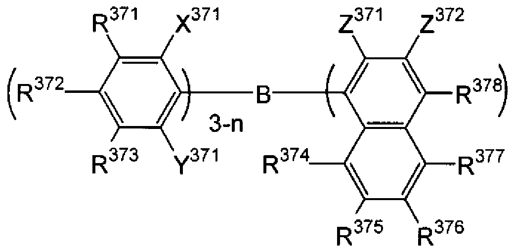
[化 25] [Chemical 25]
Figure imgf000031_0001
(式中、 Rd"〜Rd 及び Zd "は、それぞれ独立に、水素原子、飽和もしくは不飽和の 炭化水素基、芳香族基、ヘテロ環基、置換アミノ基、置換ボリル基、アルコキシ基又 はァリールォキシ基を示し、 χ371、 γ371及び z371は、それぞれ独立に、飽和もしくは不 飽和の炭化水素基、芳香族基、ヘテロ環基、置換アミノ基、アルコキシ基又はァリー ルォキシ基を示し、 Z371と Z372の置換基は相互に結合して縮合環を形成してもよぐ n は 1〜3の整数を示し、 nが 2以上の場合、 Z371は異なってもよい。但し、 nが 1、 X371、 Y371及び R372カ チル基であって、 R378が水素原子又は置換ボリル基の場合、及び n 力^で Z371がメチル基の場合を含まない。 ) (In the formula, R d ″ to R d and Z d ″ are each independently a hydrogen atom, a saturated or unsaturated hydrocarbon group, an aromatic group, a heterocyclic group, a substituted amino group, a substituted boryl group, or an alkoxy group. Each represents an aryloxy group, and χ 371 , γ 371 and z 371 each independently represent a saturated or unsaturated hydrocarbon group, aromatic group, heterocyclic group, substituted amino group, alkoxy group or aryloxy group. , Z 371 and Z 372 may be bonded to each other to form a condensed ring. N represents an integer of 1 to 3, and when n is 2 or more, Z 371 may be different. , N is 1, X 371 , Y 371 and R 372 acetyl group, R 378 is a hydrogen atom or a substituted boryl group, and n force ^ and Z 371 is a methyl group.
特開平 10— 088121に示されて 、る下記式で示される化合物  A compound represented by the following formula shown in JP-A-10-088121
[化 26]  [Chemical 26]
Figure imgf000031_0002
(式中、 及び Qdi"は、それぞれ独立に、下記式で示される配位子を表し、 81は 、ハロゲン原子、置換もしくは未置換のアルキル基、置換もしくは未置換のシクロアル キル基、置換もしくは未置換のァリール基、置換もしくは未置換の複素環基、 OR39 (R391は水素原子、置換もしくは未置換のアルキル基、置換もしくは未置換のシクロ アルキル基、置換もしくは未置換のァリール基又は置換もしくは未置換の複素環基 である。)又は— O Ga— Q391 (Q392) (Q391及び Q392は、 Q381及び Q382と同じ意味を 表す。)で示される配位子を表す。 ) [0071] [化 27] (Wherein, and Q di "each independently represents a ligand represented by the following formula: 81 is a halogen atom, a substituted or unsubstituted alkyl group, a substituted or unsubstituted cycloalkyl group, a substituted or Unsubstituted aryl group, substituted or unsubstituted heterocyclic group, OR 39 (R 391 is a hydrogen atom, substituted or unsubstituted alkyl group, substituted or unsubstituted cycloalkyl group, substituted or unsubstituted aryl group or substituted Or an unsubstituted heterocyclic group.) Or —O Ga—Q 391 (Q 392 ) (Q 391 and Q 392 are the same as Q 381 and Q 382. ) ) [0071] [Chemical 27]
Figure imgf000032_0001
(式中、環 A4U1及び A ^は、互いに結合した置換もしくは未置換のァリール環又は複 素環構造である。 ) (In the formula, the rings A 4U1 and A ^ are substituted or unsubstituted aryl ring or bicyclic ring structures bonded to each other.)
[0072] 上記式の配位子を形成する環 A4Cn及び A4C>2の置換基の具体的な例を挙げると、塩 素、臭素、ヨウ素、フッ素のハロゲン原子、メチル基、ェチル基、プロピル基、ブチル 基、 sec ブチル基、 tert ブチル基、ペンチル基、へキシル基、ヘプチル基、オタ チル基、ステアリル基、トリクロロメチル基等の置換もしくは未置換のアルキル基、フエ -ル基、ナフチル基、 3—メチルフエ-ル基、 3—メトキシフエ-ル基、 3—フルオロフ ェ-ル基、 3—トリクロロメチルフエ-ル基、 3—トリフルォロメチルフエ-ル基、 3— -ト 口フエ-ル基等の置換もしくは未置換のァリール基、メトキシ基、 n—ブトキシ基、 tert ブトキシ基、トリクロロメトキシ基、トリフルォロエトキシ基、ペンタフルォロプロポキシ 基、 2, 2, 3, 3—テ卜ラフルォロプロポキシ基、 1, 1, 1, 3, 3, 3 へキサフルォ口— 2 プロポキシ基、 6 (パーフルォロェチル)へキシルォキシ基等の置換もしくは未 置換のアルコキシ基、フエノキシ基、 p -トロフエノキシ基、 p— tert ブチルフエノ キシ基、 3—フルオロフエノキシ基、ペンタフルォロフエ-ル基、 3—トリフルォロメチル フエノキシ基等の置換もしくは未置換のァリールォキシ基、メチルチオ基、ェチルチ ォ基、 tert—ブチルチオ基、へキシルチオ基、ォクチルチオ基、トリフルォロメチルチ ォ基等の置換もしくは未置換のアルキルチオ基、フエ-ルチオ基、 p -トロフエ-ル チォ基、 ptert—ブチルフヱ-ルチオ基、 3—フルオロフヱ-ルチオ基、ペンタフルォ 口フエ-ルチオ基、 3 -トリフルォロメチルフエ-ルチオ基等の置換もしくは未置換の ァリールチオ基、シァノ基、ニトロ基、アミノ基、メチルァミノ基、ジェチルァミノ基、ェ チルァミノ基、ジェチルァミノ基、ジプロピルアミノ基、ジブチルァミノ基、ジフエニルァ ミノ基等のモノ又はジ置換アミノ基、ビス (ァセトキシメチル)アミノ基、ビス (ァセトキシ ェチル)アミノ基、ビスァセトキシプロピル)アミノ基、ビス(ァセトキシブチル)アミノ基 等のァシルァミノ基、水酸基、シロキシ基、ァシル基、力ルバモイル基、メチルカルバ モイル基、ジメチルカルバモイル基、ェチルカルバモイル基、ジェチルカルバモイル 基、プロィピルカルバモイル基、ブチルカルバモイル基、フエ-ルカルバモイル基等 の置換もしくは未置換の力ルバモイル基、カルボン酸基、スルフォン酸基、イミド基、 シクロペンタン基、シクロへキシル基等のシクロアルキル基、フエ-ル基、ナフチル基[0072] Specific examples of the substituents of the rings A4Cn and A4C > 2 forming the ligand of the above formula include chlorine, bromine, iodine, halogen atoms of fluorine, methyl group, ethyl group, Propyl group, butyl group, sec butyl group, tert butyl group, pentyl group, hexyl group, heptyl group, octyl group, stearyl group, trichloromethyl group and other substituted or unsubstituted alkyl groups, phenyl group, naphthyl group Group, 3-methylphenol group, 3-methoxyphenyl group, 3-fluorophenol group, 3-trichloromethylphenol group, 3-trifluoromethylphenol group, 3-to-diethyl ether Substituted or unsubstituted aryl groups such as -l group, methoxy group, n-butoxy group, tert butoxy group, trichloromethoxy group, trifluoroethoxy group, pentafluoropropoxy group, 2, 2, 3, 3— Terafluoropropoxy group, 1, 1, 1, 3, 3, 3 Hexafluoro--2 substituted or unsubstituted alkoxy group such as 2 propoxy group, 6 (perfluoroethyl) hexyloxy group, phenoxy group, p-trophenoxy group, p-tert butyl pheno Substituted or unsubstituted aryloxy groups such as xy group, 3-fluorophenoxy group, pentafluorophenyl group, 3-trifluoromethyl phenoxy group, methylthio group, ethylthio group, tert-butylthio group, Hexylthio, octylthio, trifluoromethylthio and other substituted or unsubstituted alkylthio groups, phenolthio groups, p-trophenylthio groups, ptert-butylphenylthio groups, 3-fluorophenylthio groups Substituted or unsubstituted arylthio group, cyano group, nitro group, aryl group, etc., pentafluoro oral phenylthio group, 3-trifluoromethylphenolthio group, etc. Mono- or di-substituted amino groups such as mino group, methylamino group, jetylamino group, ethylamino group, jetylamino group, dipropylamino group, dibutylamino group, diphenylamino group, bis (acetoxymethyl) amino group, bis (acetoxy) Ethyl) amino group, bisacetoxypropyl) amino group, bis (acetoxybutyl) amino group, etc., isylamino groups, hydroxyl groups, siloxy groups, acyl groups, strong rubamoyl groups, methylcarbamoyl groups, dimethylcarbamoyl groups, ethylcarbamoyl groups, Substituted or unsubstituted force rubamoyl groups such as a decylcarbamoyl group, a propylcarbamoyl group, a butylcarbamoyl group, a phenylcarbamoyl group, a carboxylic acid group, a sulfonic acid group, an imide group, a cyclopentane group, a cyclohexyl group, etc. Cycloalkyl group, phenyl group, naphthyl group
、ビフヱ-ル基、アントラ-ル基、フヱナントリル基、フルォレ -ル基、ピレ -ル基等の ァリール基、ピリジ-ル基、ビラジニル基、ピリミジニル基、ピリダジニル基、トリアジ- ル基、インドリニル基、キノリニル基、アタリジ-ル基、ピロリジニル基、ジォキサニル基 、ピベリジ-ル基、モルフオリジ-ル基、ピペラジ-ル基、カルバゾリル基、フラ -ル基 、チオフ ニル基、ォキサゾリル基、ォキサジァゾリル基、ベンゾォキサゾリル基、チア ゾリル基、チアジアゾリル基、ベンゾチアゾリル基、トリァゾリル基、イミダゾリル基、ベ ンゾイミダゾリル基等の複素環基等がある。また、以上の置換基同士が結合してさら なる 6員ァリール環もしくは複素環を形成してもよ 、。 , Bifuryl group, anthral group, phenanthryl group, fluorol group, pyrel group, etc. Quinolinyl group, attaridyl group, pyrrolidinyl group, dioxanyl group, piperidyl group, morpholydyl group, piperazyl group, carbazolyl group, fulleryl group, thiophenyl group, oxazolyl group, oxadiazolyl group, benzoxa Examples thereof include heterocyclic groups such as zolyl group, thiazolyl group, thiadiazolyl group, benzothiazolyl group, triazolyl group, imidazolyl group, and benzoimidazolyl group. In addition, the above substituents may be bonded to each other to form a further 6-membered aryl ring or heterocyclic ring.
[0073] 本発明の好ましい形態に、電子を輸送する領域又は陰極と有機層の界面領域に、 還元性ドーパントを含有する素子がある。ここで、還元性ドーパントとは、電子輸送性 化合物を還元ができる物質と定義される。従って、一定の還元性を有するものであれ ば、様々なものが用いられ、例えば、アルカリ金属、アルカリ土類金属、希土類金属、 アルカリ金属の酸化物、アルカリ金属のハロゲン化物、アルカリ土類金属の酸化物、 アルカリ土類金属のハロゲンィ匕物、希土類金属の酸ィ匕物又は希土類金属のハロゲン 化物、アルカリ金属の有機錯体、アルカリ土類金属の有機錯体、希土類金属の有機 錯体力 なる群力 選択される少なくとも一つの物質を好適に使用することができる。  [0073] In a preferred embodiment of the present invention, there is an element containing a reducing dopant in an electron transporting region or an interface region between a cathode and an organic layer. Here, the reducing dopant is defined as a substance capable of reducing an electron transporting compound. Accordingly, various materials can be used as long as they have a certain reducibility, such as alkali metals, alkaline earth metals, rare earth metals, alkali metal oxides, alkali metal halides, alkaline earth metals. Oxides, alkaline earth metal halides, rare earth metal oxides or rare earth metal halides, alkali metal organic complexes, alkaline earth metal organic complexes, rare earth metal organic complex forces Any one of the above-mentioned substances can be preferably used.
[0074] また、より具体的に、好ましい還元性ドーパントとしては、 Na (仕事関数: 2. 36eV) 、K (仕事関数: 2. 28eV)、Rb (仕事関数: 2. 16eV)及び Cs (仕事関数: 1. 95eV) 力 なる群力 選択される少なくとも一つのアルカリ金属や、 Ca (仕事関数: 2. 9eV) 、 Sr (仕事関数: 2. 0〜2. 5eV)、及び Ba (仕事関数: 2. 52eV)力 なる群力 選択 される少なくとも一つのアルカリ土類金属が挙げられる仕事関数が 2. 9eV以下のも のが特に好ましい。これらのうち、より好ましい還元性ドーパントは、 K、 Rb及び Csか らなる群力 選択される少なくとも一つのアルカリ金属であり、さらに好ましくは、 Rb又 は Csであり、最も好ましいのは、 Csである。これらのアルカリ金属は、特に還元能力 が高ぐ電子注入域への比較的少量の添加により、有機 EL素子における発光輝度 の向上や長寿命化が図られる。また、仕事関数が 2. 9eV以下の還元性ドーパントと して、これら 2種以上のアルカリ金属の組合わせも好ましぐ特に、 Csを含んだ組み合 わせ、例えば、 Csと Na、 Csと K、 Csと Rb又は Csと Naと Κとの組み合わせであること が好ましい。 Csを組み合わせて含むことにより、還元能力を効率的に発揮することが でき、電子注入域への添加により、有機 EL素子における発光輝度の向上や長寿命 化が図られる。 More specifically, preferable reducing dopants include Na (work function: 2.36 eV), K (work function: 2.28 eV), Rb (work function: 2.16 eV) and Cs (work Function: 1. 95eV) Force at least one selected alkali metal, Ca (work function: 2.9 eV), Sr (work function: 2.0 to 2.5 eV), and Ba (work function: 2. 52 eV) Forces Group Forces Particularly preferred are those having a work function of 2.9 eV or less, including at least one selected alkaline earth metal. Of these, more preferred reducing dopants are K, Rb and Cs. At least one alkali metal selected, more preferably Rb or Cs, and most preferably Cs. These alkali metals can improve emission brightness and extend the lifetime of organic EL devices by adding a relatively small amount to the electron injection region, which has a particularly high reducing ability. In addition, as a reducing dopant having a work function of 2.9 eV or less, a combination of two or more alkali metals is also preferable. Particularly, a combination containing Cs, for example, Cs and Na, Cs and K Cs and Rb or a combination of Cs, Na and Κ is preferable. By including Cs in combination, the reducing ability can be efficiently exhibited, and by adding it to the electron injection region, the emission luminance of the organic EL element can be improved and the life can be extended.
[0075] 本発明においては陰極と有機層の間に絶縁体や半導体で構成される電子注入- 輸送層をさらに設けてもよい。この時、電流のリークを有効に防止して、電子注入性 を向上させることができる。このような絶縁体としては、アルカリ金属カルコゲナイド、 アルカリ土類金属カルコゲナイド、アルカリ金属のハロゲンィ匕物及びアルカリ土類金 属のハロゲンィ匕物力 なる群力 選択される少なくとも一つの金属化合物を使用する のが好ましい。電子注入'輸送層がこれらのアルカリ金属カルコゲナイド等で構成さ れていれば、電子注入性をさらに向上させることができる点で好ましい。具体的に、 好ましいアルカリ金属カルコゲナイドとしては、例えば、 Li 0、 LiO、 Na S、 Na Se及  In the present invention, an electron injection / transport layer made of an insulator or a semiconductor may be further provided between the cathode and the organic layer. At this time, current leakage can be effectively prevented, and the electron injection property can be improved. As such an insulator, at least one metal compound selected from the group consisting of alkali metal chalcogenides, alkaline earth metal chalcogenides, alkali metal halides and alkaline earth metal halides is used. preferable. If the electron injecting / transporting layer is composed of these alkali metal chalcogenides or the like, it is preferable in that the electron injecting property can be further improved. Specifically, preferred alkali metal chalcogenides include, for example, Li 0, LiO, Na S, Na Se and
2 2 2 び NaOが挙げられ、好ましいアルカリ土類金属カルコゲナイドとしては、例えば、 Ca 0、 BaO、 SrO、 BeO、 BaS、及び CaSeが挙げられる。また、好ましいアルカリ金属 のハロゲン化物としては、例えば、 LiF、 NaF、 KF、 LiCl、 KCl及び NaCl等が挙げら れる。また、好ましいアルカリ土類金属のハロゲン化物としては、例えば、 CaF、 BaF  2 2 2 and NaO are preferable, and preferable alkaline earth metal chalcogenides include, for example, Ca 0, BaO, SrO, BeO, BaS, and CaSe. Preferred alkali metal halides include, for example, LiF, NaF, KF, LiCl, KCl, and NaCl. Preferred alkaline earth metal halides include, for example, CaF, BaF
2 2
、 SrF、 MgF及び BeFといったフッ化物や、フッ化物以外のハロゲン化物が挙げFluorides such as SrF, MgF and BeF, and halides other than fluoride
2 2 2 2 2 2 2 2
られる。  It is done.
[0076] また、電子注入'輸送層を構成する半導体としては、 Ba、 Ca、 Sr、 Yb、 Al、 Ga、 In 、 Li、 Na、 Cd、 Mg、 Si、 Ta、 Sb及び Znの少なくとも一つの元素を含む酸化物、窒 化物又は酸ィヒ窒化物等の一種単独又は二種以上の組み合わせが挙げられる。また 、電子注入 ·輸送層を構成する無機化合物が、微結晶又は非晶質の絶縁性薄膜で あることが好ま ヽ。電子注入 ·輸送層がこれらの絶縁性薄膜で構成されて ヽれば、 より均質な薄膜が形成されるために、ダークスポット等の画素欠陥を減少させることが できる。尚、このような無機化合物としては、上述したアルカリ金属カルコゲナイド、ァ ルカリ土類金属カルコゲナイド、アルカリ金属のハロゲン化物及びアルカリ土類金属 のハロゲンィ匕物等が挙げられる。 [0076] Further, the semiconductor constituting the electron injection 'transport layer includes at least one of Ba, Ca, Sr, Yb, Al, Ga, In, Li, Na, Cd, Mg, Si, Ta, Sb, and Zn. One kind or a combination of two or more kinds of oxides, nitrides, and oxynitrides containing elements can be used. In addition, the inorganic compound constituting the electron injecting / transporting layer is preferably a microcrystalline or amorphous insulating thin film. If the electron injection / transport layer is made of these insulating thin films, Since a more uniform thin film is formed, pixel defects such as dark spots can be reduced. Examples of such inorganic compounds include the above-mentioned alkali metal chalcogenides, alkali earth metal chalcogenides, alkali metal halides and alkaline earth metal halides.
[0077] 5. 中間接続層  [0077] 5. Intermediate connection layer
中間接続層はァクセプター層 Zドナー層 Z電子輸送材料層の積層体であり、二つ の発光層を接続するために用いられる。  The intermediate connection layer is a laminate of an acceptor layer, a Z donor layer, and a Z electron transport material layer, and is used to connect two light emitting layers.
[0078] [ァクセプター層] [0078] [Acceptor layer]
ァクセプターは、易還元性の有機化合物である。  The acceptor is an easily reducible organic compound.
化合物の還元しやすさは、還元電位で測定することができる。本発明では飽和カロ メル(SCE)電極を参照電極とした還元電位において、好ましくは 0. 8V以上、より 好ましくは一 0. 3V以上であり、特に好ましくはテトラシァノキノジメタン (TCNQ)の還 元電位 (約 OV)より大きな値を持つ化合物が好ま 、。  The ease of reduction of a compound can be measured by a reduction potential. In the present invention, the reduction potential using a saturated calomel (SCE) electrode as a reference electrode is preferably 0.8 V or more, more preferably 1 0.3 V or more, and particularly preferably tetracyanoquinodimethane (TCNQ). Compounds with values greater than the original potential (about OV) are preferred.
[0079] ァクセプターは、好ましくは、電子吸引性の置換基又は電子欠乏環を有する有機 化合物である。 [0079] The acceptor is preferably an organic compound having an electron-withdrawing substituent or an electron-deficient ring.
電子吸引性の置換基として、例えば、ハロゲン、 CN—、カルボ-ル基、ァリールホ ゥ素基等が挙げられる。  Examples of the electron-withdrawing substituent include halogen, CN—, carbo group, aryl group and the like.
電子欠乏環として、 f列えば、、 2 ピリジノレ、 3 ピリジノレ、 4 ピリジノレ、 2 キノリノレ、 3 キノリル、 4 キノリル、 2 イミダゾール、 4 イミダゾール、 3 ピラゾール、 4 ピ ラゾール、ピリダジン、ピリミジン、ピラジン、シンノリン、フタラジン、キナゾリン、キノキ サリン、 3— (1, 2, 4— N)—トリァゾリル、 5— (1, 2, 4— N)—トリァゾリル、 5—テトラ ゾリル、 4— (1— O, 3— N)—ォキサゾール、 5— (1— O, 3— N)—ォキサゾール、 4 (1 -S, 3-N) チアゾーノレ、 5— (1 -S, 3-N) チアゾーノレ、 2 ベンゾキサ ゾール、 2 ベンゾチアゾール、 4— (1, 2, 3-N)—ベンゾトリァゾール、及びべンズ イミダゾールカ なる群力 選択される化合物等が挙げられる力 必ずしもこれらに限 定されるわけではない。  As an electron-deficient ring, f-pyridinole, 3-pyridinole, 4-pyridinole, 2-quinolinole, 3-quinolyl, 4-quinolyl, 2-imidazole, 4-imidazole, 3-pyrazole, 4-pyrazole, pyridazine, pyrimidine, pyrazine, cinnoline, phthalazine , Quinazoline, quinoxaline, 3— (1, 2, 4—N) —triazolyl, 5— (1, 2, 4—N) —triazolyl, 5—tetrazolyl, 4— (1—O, 3—N) —Oxazole, 5— (1—O, 3—N) —Oxazole, 4 (1 -S, 3-N) thiazole, 5— (1 -S, 3-N) thiazonole, 2 benzoxazole, 2 benzothiazole, 4— (1, 2, 3-N) -benzotriazole and Benz Imidazole Force that includes the selected compound, etc. It is not necessarily limited to these.
[0080] ァクセプターは、好ましくはキノイド誘導体、ァリールボラン誘導体、チォピランジオ キシド誘導体、ナフタルイミド誘導体等のイミド誘導体、へキサァザトリフエ二レン誘導 体等がある。 [0080] The acceptor is preferably an imide derivative such as a quinoid derivative, an arylborane derivative, a thiopyrandioxide derivative or a naphthalimide derivative, or a hexazatriphenylene diene derivative. There is a body.
キノイド誘導体としては下記に示したような化合物が好ましい  As the quinoid derivative, the following compounds are preferable.
[化 28] [Chemical 28]
Figure imgf000036_0001
(式中、!^〜尺48は、それぞれ水素、ハロゲン、フルォロアルキル基、シァノ基、アルコ キシ基、アルキル基又はァリール基である。ただし、!^〜尺48が同一分子中で全て、 水素又はフッ素であるものは除く。 Xは電子吸引基であり、下記式 (j)〜(p)の構造の いずれかからなる。好ましくは、(j)、(k)、(1)の構造である。 (In the formula,! ^ To 48 are hydrogen, halogen, fluoroalkyl group, cyano group, alkoxy group, alkyl group, or aryl group, respectively, provided that! ^ To 48 are all hydrogen or Excluding those that are fluorine X is an electron-withdrawing group, and consists of any of the structures of the following formulas (j) to (p), preferably the structures of (j), (k), and (1) .
[化 29] [Chemical 29]
O NC丫 CN ^ NC丫 CF3 NC丫 COOR49 R50OOC^COOR51 NC^R52 0) (k) (I) (m) (n) (o) (p) O NC 丫 CN ^ NC 丫 CF 3 NC 丫 COOR 49 R 50 OOC ^ COOR 51 NC ^ R 52 0) (k) (I) (m) (n) (o) (p)
(式中、 R49〜R52は、それぞれ水素、フルォロアルキル基、アルキル基、ァリール基 又は複素環基であり、 R5°と R51が環を形成してもよい。 )
Figure imgf000037_0001
[0083] ァリールボラン誘導体として、下記構造を有する化合物が好ましい
(In the formula, R 49 to R 52 are each hydrogen, a fluoroalkyl group, an alkyl group, an aryl group, or a heterocyclic group, and R 5 ° and R 51 may form a ring.)
Figure imgf000037_0001
[0083] As the arylborane derivative, a compound having the following structure is preferable.
[化 31]  [Chemical 31]
Figure imgf000038_0001
(2a) (2b)  (2a) (2b)
(式中、 Ai:1〜 Ar7は、それぞれ電子吸引基を有するァリール基 (複素環を含む)であ る。 Ar8は、電子吸引基を有するァリーレン基である。 Sは 1又は 2である。 ) (In the formula, Ai: 1 to Ar 7 are each an aryl group (including a heterocyclic ring) having an electron withdrawing group. Ar 8 is an arylene group having an electron withdrawing group. S is 1 or 2 is there. )
[0084] ァリールボラン誘導体の具体例としては、以下の化合物が挙げられる。  [0084] Specific examples of the arylborane derivative include the following compounds.
[化 32]  [Chemical 32]
Figure imgf000038_0002
[0085] 特に好ましくは、少なくとも一個のフッ素をァリールへの置換基として有する化合物 であり、トリス j8— (ペンタフルォロナフチル)ボラン (PNB)等があげられる。  [0085] Particularly preferred is a compound having at least one fluorine as a substituent on the aryl, such as tris j8- (pentafluoronaphthyl) borane (PNB).
[0086] イミド誘導体として、好ましくは、ナフタレンテトラカルボン酸ジイミドィ匕合物及びピロ メリット酸ジイミド化合物である。  [0086] The imide derivative is preferably a naphthalene tetracarboxylic acid diimide compound or a pyromellitic acid diimide compound.
[0087] チォピランジオキシド誘導体として、下記式(3a)に示される化合物が、チォキサン テンジォキシド誘導体として、下記式 (3b)に示される化合物が、それぞれ挙げられる [化 33] [0087] Examples of the thiopyran dioxide derivative include a compound represented by the following formula (3a), and examples of the thioxanthene dioxide derivative include a compound represented by the following formula (3b). [Chemical 33]
Figure imgf000039_0001
(3a) (3b) 式(3a)及び式(3b)において、 R53〜R64は、それぞれ水素、ハロゲン、フルォロア ルキル基、シァノ基、アルキル基又はァリール基である。好ましくは、水素、シァノ基 である。 (3a) (3b) In formula (3a) and formula (3b), R 53 to R 64 are each hydrogen, halogen, fluoroalkyl group, cyano group, alkyl group or aryl group. Of these, hydrogen and cyano group are preferable.
式(3a)及び式(3b)にお!/、て、 Xは電子吸弓 I基を示し式( la)〜(: Li)の Xと同じであ る。好ましくは、(j)、(k)、(1)の構造である。  In the formula (3a) and the formula (3b),! /, X represents the electron-absorbing I group and is the same as X in the formulas (la) to (: Li). Preferably, the structure is (j), (k), or (1).
[0088] R53〜R64が示すハロゲン、フルォロアルキル基、アルキル基及びァリール基は 1^〜 R48と同様である。 [0088] halogen R 53 to R 64 represents, Furuoroarukiru group, an alkyl group and Ariru group is the same as 1 ^ ~ R 48.
[0089] 式(3a)に示されるチォピランジオキシド誘導体、式(3b)に示されるチォキサンテン ジォキシド誘導体の具体例を以下に示す。  Specific examples of the thiopyran dioxide derivative represented by the formula (3a) and the thioxanthene dioxide derivative represented by the formula (3b) are shown below.
[化 34]  [Chemical 34]
Figure imgf000039_0002
(式中、 tBuは t プチル基である。)
Figure imgf000039_0002
(In the formula, tBu is a t-butyl group.)
[0090] さらに上記の式(la)〜(: Li)、(3a)〜(3b)において、電子吸引性基 Xは、下記式で 表される置換基 (X)又は (y)でもよ ヽ。 Further, in the above formulas (la) to (: Li) and (3a) to (3b), the electron withdrawing group X may be a substituent (X) or (y) represented by the following formula: .
[化 35]
Figure imgf000040_0001
[Chemical 35]
Figure imgf000040_0001
[0091] 式中、 Ar9及び Arlc>は置換もしくは無置換の複素環、置換もしくは無置換のァリー ルォキシカルボ-ル又はアルデヒドであり、好ましくは、ピリジン、ピラジン、キノキサリ ンである。 Ar9と Ar は互いに連結し 5員又は 6員の環状構造を形成してもよい。 In the formula, Ar 9 and Ar lc> are a substituted or unsubstituted heterocyclic ring, a substituted or unsubstituted aryloxycarbon or aldehyde, preferably pyridine, pyrazine, or quinoxaline. Ar 9 and Ar may be connected to each other to form a 5-membered or 6-membered cyclic structure.
[0092] へキサァザトリフエ-レン誘導体としては下記に挙げられる構造が好ましぐ特に好 ましくはシァノ基を有する化合物である。  [0092] The hexazatriphenylene derivative is preferably a compound having a cyano group, particularly preferably a structure shown below.
[化 36]  [Chemical 36]
Figure imgf000040_0002
(式中、 Rb5は、それぞれ、シァノ基、ァリールォキシカルボ-ル基、アルコキシカルボ ニル基、ジアルキル力ルバモイル基、ジァリール力ルバモイル基、ハロゲン原子、 -ト 口基、又はカルボキシル基である。 ) (In the formula, R b5 is a cyano group, an arylcarbonyl group, an alkoxycarbonyl group, a dialkyl group rubermoyl group, a diaryl group rubermoyl group, a halogen atom, a -ortho group, or a carboxyl group, respectively. )
ァクセプターは、好ましくは、薄膜形成性を有する。即ち、蒸着でァクセプター層を 形成できる。「薄膜を形成できる」とは基板上に真空蒸着、スピンコート等の一般的な 薄膜形成方法にて平坦な薄膜を作成できることである。ここで平坦とは、薄膜の凹凸 が小さいということであり、好ましくは、面粗さ(Ra)が lOnm以下であり、より好ましくは 、面粗さ (Ra)が 1. 5nm以下であり、さらに好ましくは、面粗さ(Ra)が lnm以下であ る。尚、面粗さは原子間力顕微鏡 (AFM)により測定ができる。 薄膜形成性を有する有機化合物として、好ましくは非晶性の有機化合物であり、よ り好ましくは、非晶性のキノジメタン誘導体であり、さらに好ましくは非晶性かつ CN— 基の数が 5以上のキノジメタン誘導体である。例えば、上記の(CN) —TCNQが挙 The acceptor preferably has a thin film forming property. That is, the acceptor layer can be formed by vapor deposition. “A thin film can be formed” means that a flat thin film can be formed on a substrate by a general thin film forming method such as vacuum deposition or spin coating. Here, flat means that the unevenness of the thin film is small, preferably the surface roughness (Ra) is lOnm or less, more preferably, the surface roughness (Ra) is 1.5 nm or less, Preferably, the surface roughness (Ra) is 1 nm or less. The surface roughness can be measured with an atomic force microscope (AFM). The organic compound having a thin film forming property is preferably an amorphous organic compound, more preferably an amorphous quinodimethane derivative, and further preferably amorphous and having 5 or more CN-groups. It is a quinodimethane derivative. For example, (CN) -TCNQ above
2  2
げられる。  I can get lost.
[0094] ァクセプター層に含まれるァクセプターの含有量は、好ましくは層全体に対して 1〜 100モル0 /0であり、より好ましくは 50〜: LOOモル0 /0である。 [0094] The content of Akuseputa contained in Akuseputa layer is preferably from 1 to 100 mole 0/0 for the entire layer, and more preferably 50 to: a LOO mol 0/0.
ァクセプター層は、ァクセプターの他に、正孔輸送性で光透過性のあるものを含有 できる力 必ずしもこれに限定されるものではない。  In addition to the acceptor, the acceptor layer is capable of containing a hole-transporting and light-transmitting material, but is not necessarily limited thereto.
ァクセプター層の膜厚は、好ましくは、 l〜100nmである。  The thickness of the acceptor layer is preferably 1 to 100 nm.
[0095] [ドナー層] [0095] [Donor layer]
本発明の有機 EL素子において、ドナー層とは、ドナー性金属、ドナー性金属化合 物及びドナー性金属錯体力も選ばれる群のうち少なくとも一種を、ドナーとして含有 する層である。  In the organic EL device of the present invention, the donor layer is a layer containing, as a donor, at least one selected from the group in which a donor metal, a donor metal compound, and a donor metal complex force are also selected.
[0096] ドナー性金属とは、仕事関数 3. 8eV以下の金属をいい、好ましくはアルカリ金属、 アルカリ土類金属及び希土類金属であり、より好ましくは Cs, Li, Na, Sr, K, Mg, C a, Ba, Yb, Eu及び Ceである 0 [0096] The donor metal means a metal having a work function of 3.8 eV or less, preferably an alkali metal, an alkaline earth metal and a rare earth metal, more preferably Cs, Li, Na, Sr, K, Mg, 0 which is Ca, Ba, Yb, Eu and Ce
[0097] ドナー性金属化合物とは、上記のドナー性金属を含む化合物であり、好ましくはァ ルカリ金属、アルカリ土類金属又は希土類金属を含む化合物であり、より好ましくはこ れらの金属のハロゲンィ匕物、酸化物、炭酸塩、ホウ酸塩である。例えば、 MO (Mは ドナー性金属、 Xは 0. 5〜1. 5)、 MF (Xは 1〜3)、 M (CO ) (xは 0. 5〜1. 5)で表  [0097] The donor metal compound is a compound containing the above donor metal, preferably a compound containing alkali metal, alkaline earth metal, or rare earth metal, and more preferably halogenated metal of these metals. It is porridge, oxide, carbonate, borate. For example, MO (M is a donor metal, X is 0.5 to 1.5), MF (X is 1 to 3), M (CO) (x is 0.5 to 1.5).
3  Three
される化合物である。  It is a compound.
[0098] ドナー性金属錯体とは、上記のドナー性金属の錯体であり、好ましくはアルカリ金属 、アルカリ土類金属又は希土類金属の有機金属錯体である。好ましくは下記式 (I)で 表される有機金属錯体である。  [0098] The donor metal complex is a complex of the above donor metal, and preferably an alkali metal, alkaline earth metal, or rare earth metal organometallic complex. Preferred is an organometallic complex represented by the following formula (I).
[化 37]
Figure imgf000041_0001
(式中、 Mはドナー性金属であり、 Qは配位子であり、好ましくはカルボン酸誘導体、 ジケトン誘導体、キノリン誘導体であり、 nは 1〜4の整数である。 )
[Chemical 37]
Figure imgf000041_0001
(In the formula, M is a donor metal, Q is a ligand, preferably a carboxylic acid derivative, a diketone derivative, or a quinoline derivative, and n is an integer of 1 to 4.)
ドナー性金属錯体の具体例としては、特開 2005— 72012号公報に記載のタンダ ステン水車等が挙げられる。さらに、特開平 11— 345687号公報に記載された中心 金属がアルカリ金属、アルカリ土類金属であるフタロシア-ンィ匕合物等もドナー性金 属錯体として使用できる。  As a specific example of the donor metal complex, there is a tandasten turbine described in JP-A-2005-72012. Furthermore, phthalocyanine compounds whose central metals are alkali metals and alkaline earth metals described in JP-A-11-345687 can also be used as donor metal complexes.
[0099] 上記のドナーは一種単独で使用してもよいし、二種以上を組み合わせて使用して ちょい。 [0099] The above donors may be used alone or in combination of two or more.
ドナー層に含まれるドナーの含有量は、好ましくは、層全体に対して 1〜: LOOモル %であり、より好ましくは 50〜: LOOモル0 /0である。 The content of the donor contained in the donor layer is preferably 1 to the entire layer: a LOO mol%, more preferably 50 to: a LOO mol 0/0.
ドナー層は、上記のドナーの他に、光透過性のある物質であれば、単一又は複数 種類の物質を含有できる。具体的には、ァミン化合物、縮合環化合物、含窒素環化 合物、金属錯体等の有機物や、金属酸化物、金属窒化物、金属フッ化物、炭酸塩等 の無機物を用いることができる力 必ずしもこれに限定されるものではない。  The donor layer can contain a single substance or a plurality of kinds of substances as long as it is a light-transmitting substance in addition to the donor. Specifically, the ability to use organic substances such as amine compounds, condensed ring compounds, nitrogen-containing cyclic compounds, metal complexes, and inorganic substances such as metal oxides, metal nitrides, metal fluorides, and carbonates. It is not limited to this.
ドナー層の膜厚は、好ましくは、 1〜: LOOnmである。  The thickness of the donor layer is preferably 1 to: LOOnm.
[0100] [電子輸送材料層] [0100] [Electron transport material layer]
電子輸送材料層には、非錯体の含窒素複素環構造を含む化合物を用いる。好まし くは含窒素 5員複素環構造を含む化合物である。具体的には、下記式(1)で表され る化合物が好ましい。  For the electron transport material layer, a compound containing a non-complex nitrogen-containing heterocyclic structure is used. A compound containing a nitrogen-containing 5-membered heterocyclic structure is preferred. Specifically, a compound represented by the following formula (1) is preferable.
[化 38]  [Chemical 38]
Figure imgf000042_0001
(式中、!^〜 はそれぞれ、水素原子、置換もしくは無置換の核原子数 5〜60のァリ ール基、置換もしくは無置換の核原子数 5〜60のへテロアリール基、置換もしくは無 置換の炭素数 1〜50のアルキル基、置換もしくは無置換の炭素数 3〜50のシクロア ルキル基、置換もしくは無置換の核原子数 6〜50のァラルキル基、置換もしくは無置 換の炭素数 1〜50のアルコキシ基、置換もしくは無置換の核原子数 5〜50のァリー ルォキシ基、置換もしくは無置換の核原子数 5〜50のァリールチオ基、置換もしくは 無置換の炭素数 1〜50のアルコキシカルボニル基、置換もしくは無置換の核原子数 5〜50のァリール基で置換されたァミノ基、ハロゲン原子、シァノ基、ニトロ基、ヒドロ キシル基又はカルボキシル基であり、 (Wherein ^^ is a hydrogen atom, a substituted or unsubstituted aryl group having 5 to 60 nuclear atoms, a substituted or unsubstituted heteroaryl group having 5 to 60 nuclear atoms, a substituted or unsubstituted group, respectively. A substituted alkyl group having 1 to 50 carbon atoms, a substituted or unsubstituted cyclohexane having 3 to 50 carbon atoms Alkyl group, substituted or unsubstituted aralkyl group having 6 to 50 nuclear atoms, substituted or unsubstituted alkoxy group having 1 to 50 carbon atoms, substituted or unsubstituted aryloxy group having 5 to 50 nuclear atoms, substituted Or an unsubstituted aryloxy group having 5 to 50 nuclear atoms, a substituted or unsubstituted alkoxycarbonyl group having 1 to 50 carbon atoms, an amino group substituted with a substituted or unsubstituted arylene group having 5 to 50 nuclear atoms, A halogen atom, cyano group, nitro group, hydroxyl group or carboxyl group,
!^〜 の隣り合う置換基の一組が互いに結合して芳香環又は複素環を形成して いてもよい。 )  ! A set of adjacent substituents of ^ to may be bonded to each other to form an aromatic ring or a heterocyclic ring. )
また、下記式(2)で表される化合物を使用できる。  Moreover, the compound represented by following formula (2) can be used.
[化 39] [Chemical 39]
Figure imgf000043_0001
(式中、 R9〜R2°はそれぞれ、水素原子、置換もしくは無置換の核原子数 5〜60のァ リール基、置換もしくは無置換の核原子数 5〜60のへテロアリール基、置換もしくは 無置換の炭素数 1〜50のアルキル基、置換もしくは無置換の炭素数 3〜50のシクロ アルキル基、置換もしくは無置換の核原子数 6〜50のァラルキル基、置換もしくは無 置換の炭素数 1〜50のアルコキシ基、置換もしくは無置換の核原子数 5〜50のァリ ールォキシ基、置換もしくは無置換の核原子数 5〜50のァリールチオ基、置換もしく は無置換の炭素数 1〜50のアルコキシカルボニル基、置換もしくは無置換の核原子 数 5〜50のァリール基で置換されたァミノ基、ハロゲン原子、シァノ基、ニトロ基、ヒド 口キシル基又はカルボキシル基であり、 R9〜R2の隣り合う基が互いに結合して芳香 環を形成していてもよぐ R9〜R2の少なくとも 1つは下記式で示される置換基である (In the formula, R 9 to R 2 ° are each a hydrogen atom, a substituted or unsubstituted aryl group having 5 to 60 nuclear atoms, a substituted or unsubstituted heteroaryl group having 5 to 60 nuclear atoms, substituted or unsubstituted, An unsubstituted alkyl group having 1 to 50 carbon atoms, a substituted or unsubstituted cycloalkyl group having 3 to 50 carbon atoms, a substituted or unsubstituted aralkyl group having 6 to 50 nuclear atoms, a substituted or unsubstituted carbon number 1 ~ 50 alkoxy group, substituted or unsubstituted aryloxy group having 5 to 50 carbon atoms, substituted or unsubstituted aryloxy group having 5 to 50 nucleus atoms, substituted or unsubstituted carbon atoms 1 to 50 An alkoxycarbonyl group, an amino group substituted with a substituted or unsubstituted aryl group having 5 to 50 nuclear atoms, a halogen atom, a cyano group, a nitro group, a hydroxy group, or a carboxyl group, and R 9 to R 2 Adjacent groups of At least one of Yogu R 9 to R 2 also form an aromatic ring Te is a substituent represented by the following formula
[化 40] (Lは、置換もしくは無置換の炭素数 6〜60のァリーレン基、置換もしくは無置換の炭 素数 5〜60のへテロアリーレン基、又は置換もしくは無置換のフルォレニレン基であ り、 [Chemical 40] (L is a substituted or unsubstituted arylene group having 6 to 60 carbon atoms, a substituted or unsubstituted heteroarylene group having 5 to 60 carbon atoms, or a substituted or unsubstituted fluorenylene group,
Ar1は、置換もしくは無置換の炭素数 6〜60のァリーレン基、置換もしくは無置換の ピリジ-レン基又は置換もしくは無置換のキノリ-レン基であり、 Ar 1 is a substituted or unsubstituted arylene group having 6 to 60 carbon atoms, a substituted or unsubstituted pyridylene group, or a substituted or unsubstituted quinolylene group,
Ar2は、水素原子、置換もしくは無置換の核原子数 5〜60のァリール基、置換もしく は無置換のピリジル基、置換もしくは無置換のキノリル基、置換もしくは無置換の炭素 数 1〜50のアルキル基、置換もしくは無置換の炭素数 3〜50のシクロアルキル基、置 換もしくは無置換の核原子数 6〜50のァラルキル基、置換もしくは無置換の炭素数 1 〜50のアルコキシ基、置換もしくは無置換の核原子数 5〜50のァリールォキシ基、 置換もしくは無置換の核原子数 5〜50のァリールチオ基、置換もしくは無置換の炭 素数 1〜50のアルコキシカルボ-ル基、置換もしくは無置換の核原子数 5〜50のァ リール基で置換されたァミノ基、ハロゲン原子、シァノ基、ニトロ基、ヒドロキシル基又 はカルボキシル基である。 ) ) Ar 2 is a hydrogen atom, a substituted or unsubstituted aryl group having 5 to 60 nuclear atoms, a substituted or unsubstituted pyridyl group, a substituted or unsubstituted quinolyl group, a substituted or unsubstituted carbon number of 1 to 50. Alkyl group, substituted or unsubstituted cycloalkyl group having 3 to 50 carbon atoms, substituted or unsubstituted aralkyl group having 6 to 50 nuclear atoms, substituted or unsubstituted alkoxy group having 1 to 50 carbon atoms, substituted Or an unsubstituted aryloxy group having 5 to 50 nuclear atoms, a substituted or unsubstituted aryloxy group having 5 to 50 nuclear atoms, a substituted or unsubstituted alkoxycarbon group having 1 to 50 carbon atoms, substituted or unsubstituted Or an amino group substituted with an aryl group having 5 to 50 nucleus atoms, a halogen atom, a cyano group, a nitro group, a hydroxyl group or a carboxyl group. ))
上記式(2)で表される化合物の具体例を以下に例示する。  Specific examples of the compound represented by the formula (2) are illustrated below.
[化 41] [Chemical 41]
Figure imgf000044_0001
d-a) (1-b)  d-a) (1-b)
Figure imgf000044_0002
(式中において、 Rla〜R5c、 L〜L、 Arla〜Ar2cは、上記式(2)における R9〜R2°、 L a c
Figure imgf000044_0002
(In the formula, R la to R 5c , L to L, Ar la to Ar 2c are R 9 to R 2 ° in the above formula (2), L ac
、 Ar2とそれぞれ同じである。 ) And Ar 2 are the same. )
[0103] L〜L及び Arla〜Arleは、好ましくは置換もしくは無置換のフエ-レン基、置換もし a c [0103] L to L and Ar la to Ar le are preferably substituted or unsubstituted phenylene groups, substituted ac
くは無置換のビフヱ-レン基、置換もしくは無置換のナフチレン基又は置換もしくは 無置換のアントラセ-レン基、置換もしくは無置換のピリジレン基である。より好ましく はフエ-レン基、メチル基で置換されたフエ-レン基、ビフエ-レン基、ナフチレン基 又はアントラセニレン基である。  Or an unsubstituted bibutylene group, a substituted or unsubstituted naphthylene group, a substituted or unsubstituted anthracene group, or a substituted or unsubstituted pyridylene group. More preferred are a phenylene group, a phenylene group substituted with a methyl group, a biphenylene group, a naphthylene group, or an anthracenylene group.
Ar2a〜Ar2eは、好ましくは置換もしくは無置換のフエ-ル基、置換もしくは無置換の ビフエ-ル基、置換もしくは無置換のターフェニル基、置換もしくは無置換のナフチ ル基、置換もしくは無置換の炭素数 6〜20のァリール基である。より好ましくはフエ- ル基、メチル基で置換されたフヱ-ル基、ビフヱ-ル基、ターフヱ -ル基、ナフチル基 、ナフチル基で置換されたフエ-ル基である。 Ar 2a to Ar 2e are preferably substituted or unsubstituted phenyl group, substituted or unsubstituted biphenyl group, substituted or unsubstituted terphenyl group, substituted or unsubstituted naphthyl group, substituted or unsubstituted A substituted aryl group having 6 to 20 carbon atoms. More preferred are a phenyl group, a phenyl group substituted with a methyl group, a biphenyl group, a turfyl group, a naphthyl group, and a phenyl group substituted with a naphthyl group.
Rla, Rleは、好ましくは置換もしくは無置換の炭素数 1〜6のアルキル基、置換もしく は無置換の炭素数 6〜20のァリール基である。より好ましくはメチル基、ェチル基、プ 口ピル基、ブチル基、フエ-ル基、メチル基で置換されたフエ-ル基、ビフエ二ル基、 ナフチル基である。 R la and R le are preferably a substituted or unsubstituted alkyl group having 1 to 6 carbon atoms, or a substituted or unsubstituted aryl group having 6 to 20 carbon atoms. More preferred are a methyl group, an ethyl group, a propyl group, a butyl group, a phenyl group, a phenyl group substituted with a methyl group, a biphenyl group, and a naphthyl group.
R2b, R2eは、好ましくは水素原子、置換もしくは無置換の炭素数 1〜6のアルキル基 、置換もしくは無置換の炭素数 6〜20のァリール基である。より好ましくはメチル基、 ェチル基、プロピル基、ブチル基、フエ-ル基、メチル基で置換されたフエ-ル基、ビ フエ-ル基、ナフチル基である。 R 2b and R 2e are preferably a hydrogen atom, a substituted or unsubstituted alkyl group having 1 to 6 carbon atoms, or a substituted or unsubstituted aryl group having 6 to 20 carbon atoms. More preferred are a methyl group, an ethyl group, a propyl group, a butyl group, a phenyl group, a phenyl group substituted with a methyl group, a biphenyl group, and a naphthyl group.
R3a〜R6a, R3b〜R6b, R3e〜R6eは、好ましくは水素原子、置換もしくは無置換の炭 素数 1〜6のアルキル基、置換もしくは無置換の炭素数 6〜20のァリール基、シァノ 基である。より好ましくは水素原子、メチル基、フエ-ル基、ビフエ-ル基、ナフチル基 、シァノ基、トリフルォロメチル基である。 R 3a to R 6a , R 3b to R 6b , R 3e to R 6e are preferably a hydrogen atom, a substituted or unsubstituted alkyl group having 1 to 6 carbon atoms, a substituted or unsubstituted aryl group having 6 to 20 carbon atoms. Group, cyan group. More preferred are a hydrogen atom, a methyl group, a phenol group, a biphenyl group, a naphthyl group, a cyano group, and a trifluoromethyl group.
[0104] 電子輸送材料層の膜厚は、好ましくは 0. 1〜: LOOnmである。  [0104] The thickness of the electron transporting material layer is preferably 0.1 to LOONm.
[0105] [その他]  [0105] [Others]
尚、上述したように、本発明の中間接続層は少なくとも 1っはァクセプター層 Zドナ 一層 Z電子輸送材料層の積層体であるが、他の中間接続層は公知の中間接続層 であってもよい。そのような中間接続層を構成する材料の例としては、 In, Sn, Zn, T i, Zr, Hf, V, Mo, Cu, Ga, Sr, La, Ru等の金属の酸化物、窒化物、ヨウ化物、ホ ゥ化物等を挙げることができる。また、これらの金属の複数種類からなる多元系金属 化合物を挙げることができる。その具体例としては、例えば、 ITO、 IZO、 SnO、 Zn O、 TiN、 ZrN、 HfN、 TiO、 VO、 MoO、 Cul、 InN、 GaN、 CuAlO、 CuGaO x x x x 2 2As described above, the intermediate connection layer of the present invention is a laminate of at least one acceptor layer, Z donor layer, Z electron transport material layer, and other intermediate connection layers are known intermediate connection layers. It may be. Examples of materials constituting such an intermediate connection layer include oxides and nitrides of metals such as In, Sn, Zn, Ti, Zr, Hf, V, Mo, Cu, Ga, Sr, La, and Ru. , Iodide, fluoride and the like. Moreover, the multi-component metal compound which consists of multiple types of these metals can be mentioned. Specific examples thereof include, for example, ITO, IZO, SnO, ZnO, TiN, ZrN, HfN, TiO, VO, MoO, Cul, InN, GaN, CuAlO, CuGaO xxxx 2 2
、 SrCu O、 LaB、 RuOの透明導電材料を用いることができる。この中でも特に、 ITransparent conductive materials such as SrCu 2 O, LaB, and RuO can be used. Among these, I
2 2 6 2 2 6
TO、 IZO、 SnO、 ZnO、 TiO、 VO、 MoO、 RuO等の導電性金属酸化物が好 適に用いられる。  Conductive metal oxides such as TO, IZO, SnO, ZnO, TiO, VO, MoO, and RuO are preferably used.
[0106] 発光素子の視野角特性の向上等のため、中間接続層として、低屈折率材料と前記 透明導電材料とを含む膜を用いることができる。低屈折率材料としては、金属酸化物 (SiO等)や金属フッ化物 (NaF, LiF, CaF , Na A1F , A1F , MgF , ThF , LaF x 2 3 6 3 2 4 In order to improve the viewing angle characteristics of the light emitting element, a film containing a low refractive index material and the transparent conductive material can be used as the intermediate connection layer. Low refractive index materials include metal oxides (SiO, etc.) and metal fluorides (NaF, LiF, CaF, Na A1F, A1F, MgF, ThF, LaF x 2 3 6 3 2 4
, NdF等)等の金属ハロゲンィ匕物である無機化合物、含フッ素榭脂等の有機化合Organic compounds such as inorganic compounds that are metal halides such as
4 3 4 3
物を用いることができる。  Can be used.
[実施例]  [Example]
[0107] 以下、本発明の有機 EL素子用材料及び有機 EL素子について、実施例をもとに詳 細に説明するが、本発明はその要旨を越えない限り、以下の実施例に限定されない  Hereinafter, the organic EL device material and the organic EL device of the present invention will be described in detail based on examples, but the present invention is not limited to the following examples unless it exceeds the gist thereof.
[0108] <化合物 > [0108] <Compound>
実施例及び比較例に使用した材料を以下に示す。  The materials used in Examples and Comparative Examples are shown below.
[化 42] [Chemical 42]
Figure imgf000047_0001
HT 2 HT
Figure imgf000047_0002
丄 3 ε丄 3
HT 2 HT
Figure imgf000047_0002
丄 3 ε 丄 3
Figure imgf000048_0001
9£6S0/L00ZdT/13d 9ャ 8ム9 動 OAV <ァクセプター含有層に用いる材料の還元電位〉 9 £ 6S0 / L00ZdT / 13d 9m 8m 9 motion OAV <Reduction potential of the material used for the acceptor-containing layer>
ァクセプター Acl、 Ac2についてサイクリックボルタンメトリ測定をした。その結果、 飽和カロメル(SCE)電極を参照電極とした還元電位は 0. 07V、0. 71Vであった  Cyclic voltammetry was measured for the acceptors Acl and Ac2. As a result, the reduction potential using a saturated calomel (SCE) electrode as a reference electrode was 0.07V and 0.71V.
[0109] <評価方法 > [0109] <Evaluation method>
(1)駆動電圧  (1) Driving voltage
電流密度が lOmAZcm2となるように ITOと A1間に通電したときの電圧(単位: V)を 計測した。 Voltage when the current density is energized between the ITO and A1 so that lOmAZcm 2 (Unit: V) was measured.
(2)発光効率  (2) Luminous efficiency
電流密度 1 OmAZcm2印加時の ELスぺクトルを分光放射輝度計 CS 1000A (コ- 力ミノルタ社製)で計測し、発光効率 (単位: cd/A)を算出した。 The EL spectrum when a current density of 1 OmAZcm 2 was applied was measured with a spectral radiance meter CS 1000A (manufactured by Koryo Minolta), and the luminous efficiency (unit: cd / A) was calculated.
[0110] 実施例 1 [0110] Example 1
陽極 Z第 1有機発光層 Z中間接続層 Z第 2有機発光層 Z陰極の構成として、次の 素子構成カゝらなる有機 EL素子を作製した。  Anode Z First organic light-emitting layer Z Intermediate connection layer Z Second organic light-emitting layer Z As the configuration of the cathode, an organic EL device having the following device configuration was fabricated.
ITO ( 130) /Ac 1 (40) /HTl (40) /BH: BDl (40 ;40 : 2) /ETl (20) /LiF ( 1 . 0) /Ac 1 (40) /HTl (40) /BH: BD 1 (40 ; 40 : 2) /ETl (20) /LiF ( 1. 0) / Al(l 50)  ITO (130) / Ac 1 (40) / HTl (40) / BH: BDl (40; 40: 2) / ETl (20) / LiF (1.0) / Ac 1 (40) / HTl (40) / BH: BD 1 (40; 40: 2) / ETl (20) / LiF (1.0) / Al (l 50)
[0111] 厚み 0. 7mmのガラス基板上に、 ITOをスパッタリングにより 130nmの厚みになるよ うに成膜した。この基板をイソプロピルアルコール中で超音波洗浄を 5分間行ったの ち、 UVオゾン洗浄を 30分行い、その後この ITO電極付き基板を真空蒸着装置の基 板ホルダーに装着した。  [0111] A film of ITO was formed to a thickness of 130 nm on a 0.7 mm thick glass substrate by sputtering. This substrate was subjected to ultrasonic cleaning in isopropyl alcohol for 5 minutes, followed by UV ozone cleaning for 30 minutes, and then the substrate with the ITO electrode was mounted on the substrate holder of the vacuum deposition apparatus.
尚、予め、それぞれのモリブデン製の加熱ボートに、第 1有機発光層の正孔注入層 の材料及び中間接続層のァクセプター層の材料として Ac 1を、第 1、第 2有機発光層 の正孔輸送層の材料として HT1を、第 1及び第 2有機発光層の有機発光媒体層の ホスト材料として BHを、青色発光材料として BD1を、中間接続層の電子輸送材料層 及び第 2有機発光層の電子輸送層として ET1を、中間接続層のドナー層及び第 2有 機発光層の電子注入層として LiFを、陰極材料として A1を、それぞれ装着した。  In addition, Ac 1 was previously used as the material for the hole injection layer of the first organic light emitting layer and the material for the acceptor layer of the intermediate connection layer, and the holes of the first and second organic light emitting layers were previously placed on each molybdenum heating boat. HT1 as the material of the transport layer, BH as the host material of the organic light emitting medium layer of the first and second organic light emitting layers, BD1 as the blue light emitting material, the electron transport material layer of the intermediate connection layer and the second organic light emitting layer ET1 was attached as the electron transport layer, LiF as the electron injection layer of the intermediate connection layer and the second organic light emitting layer, and A1 as the cathode material.
[0112] まず、第 1有機発光層の正孔注入層として機能する Acl膜を膜厚 40nmで成膜し、 次いで正孔輸送層として機能する HTl膜を膜厚 40nmで成膜し、次いで第 1有機発 光層の有機発光媒体層として、化合物 BHとィ匕合物 BD1を 40 : 2の比となるように膜 厚 40nmで共蒸着した。この膜上に中間接続層の電子輸送材料層として ET1膜を膜 厚 20nmで成膜し、その後ドナー層として LiF膜を膜厚 lnmで蒸着し、次にァクセプ ター層として Ac 1膜を膜厚 40nmで成膜した。次に、この膜上に、第 2有機発光層の 正孔輸送層として機能する HT1膜を膜厚 40nmで成膜し、第 2有機発光層の有機発 光媒体層として、化合物 BHと化合物 BD1を 40 : 2の比となるように膜厚 40nmで共 蒸着した。さらに、この膜上に、第 2有機発光層の電子輸送層として機能する ET1膜 を膜厚 20nmで成膜し、電子注入層として LiF膜を膜厚 lnmで成膜し、最後に、この 膜上に陰極として機能する A1膜を膜厚 150nmで成膜し、有機 EL素子を得た。 得られた有機発光素子について評価を行った。結果を表 2に示す。 [0112] First, an Acl film functioning as a hole injection layer of the first organic light emitting layer was formed to a thickness of 40 nm, Next, an HTl film functioning as a hole transport layer is formed to a thickness of 40 nm, and then the organic light emitting medium layer of the first organic light emitting layer is formed so that the ratio of compound BH and compound BD1 is 40: 2. Co-deposited with a film thickness of 40 nm. On this film, an ET1 film is deposited as an electron transport material layer of an intermediate connection layer with a thickness of 20 nm, a LiF film is deposited as a donor layer with a thickness of 1 nm, and then an Ac1 film is deposited as an acceptor layer. The film was formed at 40 nm. Next, on this film, an HT1 film functioning as a hole transport layer of the second organic light-emitting layer is formed with a film thickness of 40 nm, and as the organic light-emitting medium layer of the second organic light-emitting layer, compound BH and compound BD1 Were co-deposited with a film thickness of 40 nm so that the ratio was 40: 2. Further, on this film, an ET1 film functioning as an electron transport layer of the second organic light-emitting layer was formed with a film thickness of 20 nm, and a LiF film was formed as an electron injection layer with a film thickness of 1 nm. Finally, this film An A1 film functioning as a cathode was deposited on the film with a thickness of 150 nm to obtain an organic EL device. The obtained organic light emitting device was evaluated. The results are shown in Table 2.
[0113] 実施例 2 [0113] Example 2
実施例 1において、中間接続層の電子輸送材料層、及び第 2有機発光層の電子輸 送層として ET1の代わりに ET2を用 Vヽたこと以外は、実施例 1と同様な方法で有機 E L素子を作製した。  In Example 1, except that ET2 was used instead of ET1 as the electron transport material layer of the intermediate connection layer and the electron transport layer of the second organic light emitting layer, the organic EL was made in the same manner as in Example 1. An element was produced.
[0114] 実施例 3 [0114] Example 3
実施例 1において、中間接続層の電子輸送材料層、及び第 2有機発光層の電子輸 送層として ET1の代わりに ET3を用 Vヽたこと以外は、実施例 1と同様な方法で有機 E L素子を作製した。  In Example 1, except that ET3 was used instead of ET1 as the electron transport material layer of the intermediate connection layer and the electron transport layer of the second organic light emitting layer, the organic EL was made in the same manner as in Example 1. An element was produced.
[0115] 実施例 4 [0115] Example 4
実施例 1において、中間接続層の電子輸送材料層、及び第 2有機発光層の電子輸 送層として ET1の代わりに ET4を用 ヽたこと以外は、実施例 1と同様な方法で有機 E L素子を作製した。  In Example 1, an organic EL device was prepared in the same manner as in Example 1 except that ET4 was used instead of ET1 as the electron transport material layer of the intermediate connection layer and the electron transport layer of the second organic light emitting layer. Was made.
[0116] 比較例 1 [0116] Comparative Example 1
実施例 1において、中間接続層の電子輸送材料層、及び第 2有機発光層の電子輸 送層として ET1の代わりに Alqを用 V、たこと以外は、実施例 1と同様な方法で有機 E L素子を作製した。  In Example 1, except that Alq was used instead of ET1 as the electron transport material layer of the intermediate connection layer and the electron transport layer of the second organic light emitting layer, the organic EL was made in the same manner as in Example 1. An element was produced.
[0117] 実施例 5 陽極 Z第 l有機発光層 Z中間接続層 Z第 2有機発光層 Z陰極の構成として、次の 素子構成カゝらなる有機 EL素子を作製した。 [0117] Example 5 Anode Z 1st organic light emitting layer Z intermediate connection layer Z 2nd organic light emitting layer Z As the configuration of the Z cathode, an organic EL device having the following device configuration was fabricated.
ITO ( 130) /Ac 2 (10) /HT2 (50) /HTl (20) /BH: BD2 (40 ;40 : 2) /ETl ( 20) /LiF (1. 0) /Ac2 (10) /HT2 (50) /HTl (20) /BH: BD2 (40 ;40 : 2) / ETl (20) /LiF (l. 0) /Al(150)  ITO (130) / Ac 2 (10) / HT2 (50) / HTl (20) / BH: BD2 (40; 40: 2) / ETl (20) / LiF (1. 0) / Ac2 (10) / HT2 (50) / HTl (20) / BH: BD2 (40; 40: 2) / ETl (20) / LiF (l. 0) / Al (150)
[0118] 厚み 0. 7mmのガラス基板上に、 ITOをスパッタリングにより 130nmの厚みになるよ うに成膜した。この基板をイソプロピルアルコール中で超音波洗浄を 5分間行ったの ち、 UVオゾン洗浄を 30分行い、その後この ITO電極付き基板を真空蒸着装置の基 板ホルダーに装着した。 [0118] A film of ITO was formed to a thickness of 130 nm by sputtering on a 0.7 mm thick glass substrate. This substrate was subjected to ultrasonic cleaning in isopropyl alcohol for 5 minutes, followed by UV ozone cleaning for 30 minutes, and then the substrate with the ITO electrode was mounted on the substrate holder of the vacuum deposition apparatus.
尚、予め、それぞれのモリブデン製の加熱ボートに、第 1有機発光層の正孔注入層 の材料及び中間接続層のァクセプター層の材料として Ac2を、第 1、第 2有機発光層 の正孔輸送層の材料として HT1及び HT2を、第 1及び第 2有機発光層の有機発光 媒体層のホスト材料として BHを、青色発光材料として BD2を、中間接続層の電子輸 送材料層及び第 2有機発光層の電子輸送層として ET1を、中間接続層のドナー層 及び第 2有機発光層の電子注入層として LiFを、陰極材料として A1を、それぞれ装 しプ  In addition, Ac2 is used as the material for the hole injection layer of the first organic light emitting layer and the material for the acceptor layer of the intermediate connection layer, and the holes are transported to the first and second organic light emitting layers. HT1 and HT2 as the material of the layer, BH as the host material of the organic light emitting medium layer of the first and second organic light emitting layers, BD2 as the blue light emitting material, the electron transport material layer and the second organic light emitting material of the intermediate connection layer ET1 as the electron transport layer of the layer, LiF as the electron injection layer of the intermediate connection layer and the second organic light emitting layer, and A1 as the cathode material, respectively.
[0119] まず、第 1有機発光層の正孔注入層として機能する Ac2膜を膜厚 lOnmで成膜し、 次いで正孔輸送層として機能する HT2/HT1積層膜を膜厚 50nm/20nmで成膜 し、次いで第 1有機発光層の有機発光媒体層として、化合物 BHと化合物 BD2を 40 : 2の比となるように膜厚 40nmで共蒸着した。この膜上に中間接続層の電子輸送材 料層として ET1膜を膜厚 20nmで成膜し、その後ドナー層として LiF膜を膜厚 lnmで 蒸着し、次にァクセプター層として Ac2膜を膜厚 lOnmで成膜した。次に、この膜上 に、第 2有機発光層の正孔輸送層として機能する HT2/HT1積層膜を膜厚 50nm Z20nmで成膜し、第 2有機発光層の有機発光媒体層として、化合物 BHと化合物 B D2を 40 : 2の比となるように膜厚 40nmで共蒸着した。さらに、この膜上に、第 2有機 発光層の電子輸送層として機能する ET1膜を膜厚 20nmで成膜し、電子注入層とし て LiF膜を膜厚 lnmで成膜し、最後に、この膜上に陰極として機能する A1膜を膜厚 1 50nmで成膜し、有機 EL素子を得た。 [0120] 比較例 2 [0119] First, an Ac2 film functioning as a hole injection layer of the first organic light emitting layer is formed with a film thickness lOnm, and then an HT2 / HT1 multilayer film functioning as a hole transport layer is formed with a film thickness of 50 nm / 20 nm. Then, as an organic light-emitting medium layer of the first organic light-emitting layer, compound BH and compound BD2 were co-deposited at a film thickness of 40 nm so as to have a ratio of 40: 2. On this film, an ET1 film is deposited with a thickness of 20 nm as an electron transport material layer for the intermediate connection layer, a LiF film is deposited with a thickness of lnm as a donor layer, and then an Ac2 film is deposited as an acceptor layer with a thickness of lOnm. The film was formed. Next, on this film, an HT2 / HT1 multilayer film functioning as a hole transport layer of the second organic light-emitting layer is formed with a film thickness of 50 nm and Z20 nm, and the compound BH is formed as the organic light-emitting medium layer of the second organic light-emitting layer. And Compound B D2 were co-deposited at a film thickness of 40 nm to a ratio of 40: 2. Further, on this film, an ET1 film functioning as an electron transport layer of the second organic light-emitting layer is formed with a film thickness of 20 nm, and a LiF film is formed as an electron injection layer with a film thickness of lnm. An A1 film functioning as a cathode was formed on the film with a film thickness of 150 nm to obtain an organic EL device. [0120] Comparative Example 2
実施例 5において、中間接続層の電子輸送材料層、及び第 2有機発光層の電子輸 送層として ET1の代わりに Alqを用 V、たこと以外は、実施例 1と同様な方法で有機 E L素子を作製した。  In Example 5, except that Alq was used instead of ET1 as the electron transport material layer of the intermediate connection layer and the electron transport layer of the second organic light-emitting layer, the organic EL was made in the same manner as in Example 1. An element was produced.
[0121] 評価結果を表 1に示す。 [0121] The evaluation results are shown in Table 1.
[表 1]  [table 1]
Figure imgf000052_0001
[0122] このように、従来電子輸送材料として知られる Alqを用いた場合に比べ、非錯体の 含窒素複素環構造を含む化合物を用いることにより、同じような色度領域において、 LZJ効率が相対的に 7〜20%向上し、電圧も 1〜4V以上低減できることを確認した 産業上の利用可能性 [0122] In this way, compared to the case of using Alq, which is conventionally known as an electron transport material, by using a compound containing a non-complex nitrogen-containing heterocyclic structure, the LZJ efficiency is relative in the same chromaticity region. The industrial applicability has been confirmed that the voltage can be reduced by 1 to 4V or more.
[0123] 本発明の有機 EL素子は、青色を始めとした各色有機 EL用材料として使用可能で あり、各種表示素子、ディスプレイ、ノ ックライト、照明光源、標識、看板、インテリア等 の分野に適用でき、特にカラーディスプレイの表示素子として適している。 [0123] The organic EL element of the present invention can be used as a material for various colors of organic EL, including blue, and can be applied to various display elements, displays, knock lights, illumination light sources, signs, signs, interiors, and the like. Particularly, it is suitable as a display element for a color display.

Claims

請求の範囲  The scope of the claims
[1] 陽極と陰極の間に少なくとも 2つの有機発光層が介在しており、  [1] At least two organic light emitting layers are interposed between the anode and the cathode,
前記有機発光層間に、少なくとも 1つの中間接続層を備え、  Comprising at least one intermediate connection layer between the organic light emitting layers,
前記中間接続層が、陰極側から、ァクセプター層、ドナー層及び非錯体の含窒素 複素環構造を含む化合物を含む電子輸送材料層をこの順に積層してなる有機エレ タトロルミネッセンス素子。  An organic electroluminescent device in which the intermediate connection layer is formed by laminating an acceptor layer, a donor layer, and an electron transport material layer containing a compound containing a non-complex nitrogen-containing heterocyclic structure in this order from the cathode side.
[2] 前記含窒素複素環構造が、含窒素 5員複素環構造である請求項 1に記載の有機 エレクトロノレミネッセンス素子。  [2] The organic electroreductive element according to claim 1, wherein the nitrogen-containing heterocyclic structure is a nitrogen-containing 5-membered heterocyclic structure.
[3] 前記電子輸送性材料層の非錯体の含窒素複素環構造を含む化合物が、下記式 ( 1)で表される化合物である請求項 1に記載の有機エレクト口ルミネッセンス素子。  [3] The organic electroluminescent device according to claim 1, wherein the compound containing a non-complex nitrogen-containing heterocyclic structure of the electron transporting material layer is a compound represented by the following formula (1).
[化 43]  [Chemical 43]
Figure imgf000053_0001
(式中、!^〜 はそれぞれ、水素原子、置換もしくは無置換の核原子数 5〜60のァリ ール基、置換もしくは無置換の核原子数 5〜60のへテロアリール基、置換もしくは無 置換の炭素数 1〜50のアルキル基、置換もしくは無置換の炭素数 3〜50のシクロア ルキル基、置換もしくは無置換の核原子数 6〜50のァラルキル基、置換もしくは無置 換の炭素数 1〜50のアルコキシ基、置換もしくは無置換の核原子数 5〜50のァリー ルォキシ基、置換もしくは無置換の核原子数 5〜50のァリールチオ基、置換もしくは 無置換の炭素数 1〜50のアルコキシカルボニル基、置換もしくは無置換の核原子数 5〜50のァリール基で置換されたァミノ基、ハロゲン原子、シァノ基、ニトロ基、ヒドロ キシル基又はカルボキシル基であり、!^〜 の隣り合う置換基の一組が互いに結合 して芳香環又は複素環を形成していてもよい。 ) (Wherein ^^ is a hydrogen atom, a substituted or unsubstituted aryl group having 5 to 60 nuclear atoms, a substituted or unsubstituted heteroaryl group having 5 to 60 nuclear atoms, a substituted or unsubstituted group, respectively. Substituted alkyl group having 1 to 50 carbon atoms, substituted or unsubstituted cycloalkyl group having 3 to 50 carbon atoms, substituted or unsubstituted aralkyl group having 6 to 50 nuclear atoms, substituted or unsubstituted carbon number 1 ~ 50 alkoxy group, substituted or unsubstituted aryloxy group having 5 to 50 nuclear atoms, substituted or unsubstituted aryloxy group having 5 to 50 nuclear atoms, substituted or unsubstituted alkoxycarbonyl having 1 to 50 carbon atoms An amino group, a halogen atom, a cyano group, a nitro group, a hydroxyl group, or a carboxyl group, substituted with an aryl group having 5 to 50 nuclear atoms, substituted or unsubstituted, and adjacent to A pair is tied together And may form an aromatic ring or a heterocyclic ring.
前記電子輸送性材料層の非錯体の含窒素複素環構造を含む化合物が、下記式( 2)で表される化合物である請求項 1に記載の有機エレクト口ルミネッセンス素子。  2. The organic electoluminescence device according to claim 1, wherein the compound containing a non-complex nitrogen-containing heterocyclic structure of the electron transporting material layer is a compound represented by the following formula (2).
[化 44]
Figure imgf000054_0001
[Chemical 44]
Figure imgf000054_0001
(式中、 R9〜R2°はそれぞれ、水素原子、置換もしくは無置換の核原子数 5〜60のァ リール基、置換もしくは無置換の核原子数 5〜60のへテロアリール基、置換もしくは 無置換の炭素数 1〜50のアルキル基、置換もしくは無置換の炭素数 3〜50のシクロ アルキル基、置換もしくは無置換の核原子数 6〜50のァラルキル基、置換もしくは無 置換の炭素数 1〜50のアルコキシ基、置換もしくは無置換の核原子数 5〜50のァリ ールォキシ基、置換もしくは無置換の核原子数 5〜50のァリールチオ基、置換もしく は無置換の炭素数 1〜50のアルコキシカルボニル基、置換もしくは無置換の核原子 数 5〜50のァリール基で置換されたァミノ基、ハロゲン原子、シァノ基、ニトロ基、ヒド 口キシル基又はカルボキシル基であり、 R9〜R2の隣り合う基が互いに結合して芳香 環を形成していてもよぐ R9〜R2の少なくとも 1つは下記式で示される置換基である (In the formula, R 9 to R 2 ° are each a hydrogen atom, a substituted or unsubstituted aryl group having 5 to 60 nuclear atoms, a substituted or unsubstituted heteroaryl group having 5 to 60 nuclear atoms, substituted or unsubstituted, An unsubstituted alkyl group having 1 to 50 carbon atoms, a substituted or unsubstituted cycloalkyl group having 3 to 50 carbon atoms, a substituted or unsubstituted aralkyl group having 6 to 50 nuclear atoms, a substituted or unsubstituted carbon number 1 ~ 50 alkoxy group, substituted or unsubstituted aryloxy group having 5 to 50 carbon atoms, substituted or unsubstituted aryloxy group having 5 to 50 nucleus atoms, substituted or unsubstituted carbon atoms 1 to 50 An alkoxycarbonyl group, an amino group substituted with a substituted or unsubstituted aryl group having 5 to 50 nuclear atoms, a halogen atom, a cyano group, a nitro group, a hydroxy group, or a carboxyl group, and R 9 to R 2 Adjacent groups of At least one of Yogu R 9 to R 2 also form an aromatic ring Te is a substituent represented by the following formula
[化 45]
Figure imgf000054_0002
[Chemical 45]
Figure imgf000054_0002
(Lは、置換もしくは無置換の炭素数 6〜60のァリーレン基、置換もしくは無置換の炭 素数 5〜60のへテロアリーレン基、又は置換もしくは無置換のフルォレニレン基であ り、 (L is a substituted or unsubstituted arylene group having 6 to 60 carbon atoms, a substituted or unsubstituted heteroarylene group having 5 to 60 carbon atoms, or a substituted or unsubstituted fluorenylene group,
Ar1は、置換もしくは無置換の炭素数 6〜60のァリーレン基、置換もしくは無置換の ピリジ-レン基又は置換もしくは無置換のキノリ-レン基であり、 Ar 1 is a substituted or unsubstituted arylene group having 6 to 60 carbon atoms, a substituted or unsubstituted pyridylene group, or a substituted or unsubstituted quinolylene group,
Ar2は、水素原子、置換もしくは無置換の核原子数 5〜60のァリール基、置換もしく は無置換のピリジル基、置換もしくは無置換のキノリル基、置換もしくは無置換の炭素 数 1〜50のアルキル基、置換もしくは無置換の炭素数 3〜50のシクロアルキル基、置 換もしくは無置換の核原子数 6〜50のァラルキル基、置換もしくは無置換の炭素数 1 〜50のアルコキシ基、置換もしくは無置換の核原子数 5〜50のァリールォキシ基、 置換もしくは無置換の核原子数 5〜50のァリールチオ基、置換もしくは無置換の炭 素数 1〜50のアルコキシカルボ-ル基、置換もしくは無置換の核原子数 5〜50のァ リール基で置換されたァミノ基、ハロゲン原子、シァノ基、ニトロ基、ヒドロキシル基又 はカルボキシル基である。 ) ) Ar 2 is a hydrogen atom, a substituted or unsubstituted aryl group having 5 to 60 nuclear atoms, a substituted or unsubstituted pyridyl group, a substituted or unsubstituted quinolyl group, a substituted or unsubstituted carbon number of 1 to 50. Alkyl group, substituted or unsubstituted cycloalkyl group having 3 to 50 carbon atoms, substituted or unsubstituted aralkyl group having 6 to 50 nuclear atoms, substituted or unsubstituted carbon number 1 ~ 50 alkoxy group, substituted or unsubstituted aryloxy group having 5 to 50 nuclear atoms, substituted or unsubstituted aryloxy group having 5 to 50 nuclear atoms, substituted or unsubstituted alkoxy carbo-carbon having 1 to 50 carbon atoms Or an amino group substituted with an aryl group having 5 to 50 substituted or unsubstituted aryl groups, a halogen atom, a cyano group, a nitro group, a hydroxyl group or a carboxyl group. ))
[5] 前記電子輸送性材料層の非錯体の含窒素複素環構造を含む化合物が、下記式 で表される化合物である請求項 4に記載の有機エレクト口ルミネッセンス素子。  5. The organic electoluminescence device according to claim 4, wherein the compound containing a non-complex nitrogen-containing heterocyclic structure of the electron transporting material layer is a compound represented by the following formula:
[化 46]  [Chem 46]
Figure imgf000055_0001
( Ar
Figure imgf000055_0002
(Ar
Figure imgf000055_0002
2とそれぞれ同じである。 Same as 2 .
[6] 前記ドナー層のドナーが、アルカリ金属、アルカリ土類金属、希土類金属、アルカリ 金属の酸化物、アルカリ金属のハロゲン化物、アルカリ土類金属の酸化物、アルカリ 土類金属のハロゲン化物、希土類金属の酸化物、希土類金属のハロゲン化物、アル カリ金属の有機錯体、アルカリ土類金属の有機錯体及び希土類金属の有機錯体で ある請求項 1〜5のいずれかに記載の有機エレクト口ルミネッセンス素子。  [6] The donor of the donor layer is an alkali metal, alkaline earth metal, rare earth metal, alkali metal oxide, alkali metal halide, alkaline earth metal oxide, alkaline earth metal halide, rare earth. 6. The organic electroluminescent device according to claim 1, which is a metal oxide, a rare earth metal halide, an alkali metal organic complex, an alkaline earth metal organic complex, or a rare earth metal organic complex.
[7] 前記ァクセプター層のァクセプターが、電子吸引性の置換基又は電子欠乏環を有 する有機化合物である請求項 1〜6のいずれかに記載の有機エレクト口ルミネッセン ス素子。 [7] The organic electoluminescence device according to any one of [1] to [6], wherein the acceptor of the acceptor layer is an organic compound having an electron-withdrawing substituent or an electron-deficient ring. S element.
前記ァクセプター層のァクセプター力 キノイド誘導体、ァリールボラン誘導体、チ オビランジオキシド誘導体、ナフタルイミド誘導体又はへキサァザトリフエ-レン誘導 体である請求項 7に記載の有機エレクト口ルミネッセンス素子。  8. The acceptor layer of the acceptor layer according to claim 7, wherein the acceptor layer is a quinoid derivative, an arylborane derivative, a thiobilan dioxide derivative, a naphthalimide derivative or a hexazatriphenylene derivative.
PCT/JP2007/059364 2006-05-11 2007-05-02 Organic electroluminescent device WO2007132678A1 (en)

Priority Applications (4)

Application Number Priority Date Filing Date Title
EP07742799A EP2018090A4 (en) 2006-05-11 2007-05-02 Organic electroluminescent device
KR1020087027475A KR101384046B1 (en) 2006-05-11 2007-05-02 Organic electroluminescent device
JP2008515489A JP5432523B2 (en) 2006-05-11 2007-05-02 Organic electroluminescence device
US12/300,345 US8076839B2 (en) 2006-05-11 2007-05-02 Organic electroluminescence device

Applications Claiming Priority (2)

Application Number Priority Date Filing Date Title
JP2006-133033 2006-05-11
JP2006133033 2006-05-11

Publications (1)

Publication Number Publication Date
WO2007132678A1 true WO2007132678A1 (en) 2007-11-22

Family

ID=38693777

Family Applications (1)

Application Number Title Priority Date Filing Date
PCT/JP2007/059364 WO2007132678A1 (en) 2006-05-11 2007-05-02 Organic electroluminescent device

Country Status (7)

Country Link
US (1) US8076839B2 (en)
EP (1) EP2018090A4 (en)
JP (1) JP5432523B2 (en)
KR (1) KR101384046B1 (en)
CN (1) CN101444142A (en)
TW (1) TW200808116A (en)
WO (1) WO2007132678A1 (en)

Cited By (9)

* Cited by examiner, † Cited by third party
Publication number Priority date Publication date Assignee Title
WO2011040607A1 (en) * 2009-10-02 2011-04-07 出光興産株式会社 Aromatic amine derivative, and organic electroluminescent element
JP2011086442A (en) * 2009-10-14 2011-04-28 Konica Minolta Holdings Inc Organic electroluminescent element and lighting system
JP2011119221A (en) * 2009-12-04 2011-06-16 Samsung Mobile Display Co Ltd Organic light-emitting device
WO2012029253A1 (en) * 2010-08-31 2012-03-08 出光興産株式会社 Nitrogen-containing aromatic heterocyclic derivative and organic electroluminescence device using same
WO2012128298A1 (en) * 2011-03-24 2012-09-27 出光興産株式会社 Bis-carbazole derivative and organic electroluminescent element using same
JP2012527089A (en) * 2009-05-13 2012-11-01 グローバル・オーエルイーディー・テクノロジー・リミテッド・ライアビリティ・カンパニー Internal connectors for organic electronic devices
JP2013127858A (en) * 2011-12-16 2013-06-27 Seiko Epson Corp Light emitting element, light emitting device, display device, and electronic apparatus
JP2014075347A (en) * 2013-11-05 2014-04-24 Konica Minolta Inc Organic electroluminescent element and lighting system
WO2016003053A1 (en) * 2014-07-01 2016-01-07 벽산페인트 주식회사 Compound for phosphorescent host and organic light-emitting element comprising same

Families Citing this family (549)

* Cited by examiner, † Cited by third party
Publication number Priority date Publication date Assignee Title
US9070884B2 (en) 2005-04-13 2015-06-30 Universal Display Corporation Hybrid OLED having phosphorescent and fluorescent emitters
US9051344B2 (en) 2005-05-06 2015-06-09 Universal Display Corporation Stability OLED materials and devices
US8586204B2 (en) 2007-12-28 2013-11-19 Universal Display Corporation Phosphorescent emitters and host materials with improved stability
CN101415718B (en) 2006-02-10 2013-05-29 通用显示公司 Metal complexes of cyclometallated imidazo[1,2-f]phenanthridine and diimidazo[1,2-a:1',2'-c]quinazoline ligands and isoelectronic and benzannulated analogs thereof
US9130177B2 (en) 2011-01-13 2015-09-08 Universal Display Corporation 5-substituted 2 phenylquinoline complexes materials for light emitting diode
US20130032785A1 (en) 2011-08-01 2013-02-07 Universal Display Corporation Materials for organic light emitting diode
KR20170065684A (en) 2007-03-08 2017-06-13 유니버셜 디스플레이 코포레이션 Phosphorescent materials
US8367850B2 (en) 2007-08-08 2013-02-05 Universal Display Corporation Benzo-fused thiophene or benzo-fused furan compounds comprising a triphenylene group
KR101665726B1 (en) 2007-08-08 2016-10-12 유니버셜 디스플레이 코포레이션 Single triphenylene chromophores in phosphorescent light emitting diodes
WO2009073245A1 (en) 2007-12-06 2009-06-11 Universal Display Corporation Light-emitting organometallic complexes
WO2009085344A2 (en) 2007-12-28 2009-07-09 Universal Display Corporation Dibenzothiophene-containing materials in phosphorescent light emitting diodes
TWI478624B (en) * 2008-03-27 2015-03-21 Nippon Steel & Sumikin Chem Co Organic electroluminescent elements
KR101778910B1 (en) 2008-06-30 2017-09-14 유니버셜 디스플레이 코포레이션 Hole transport materials containing triphenylene
WO2010027583A1 (en) 2008-09-03 2010-03-11 Universal Display Corporation Phosphorescent materials
TWI482756B (en) 2008-09-16 2015-05-01 Universal Display Corp Phosphorescent materials
WO2010036765A1 (en) 2008-09-25 2010-04-01 Universal Display Corporation Organoselenium materials and their uses in organic light emitting devices
US8367223B2 (en) * 2008-11-11 2013-02-05 Universal Display Corporation Heteroleptic phosphorescent emitters
US8815415B2 (en) 2008-12-12 2014-08-26 Universal Display Corporation Blue emitter with high efficiency based on imidazo[1,2-f] phenanthridine iridium complexes
US9067947B2 (en) 2009-01-16 2015-06-30 Universal Display Corporation Organic electroluminescent materials and devices
US11910700B2 (en) 2009-03-23 2024-02-20 Universal Display Corporation Heteroleptic iridium complexes as dopants
US8709615B2 (en) 2011-07-28 2014-04-29 Universal Display Corporation Heteroleptic iridium complexes as dopants
US8722205B2 (en) 2009-03-23 2014-05-13 Universal Display Corporation Heteroleptic iridium complex
TWI770731B (en) 2009-04-28 2022-07-11 美商環球展覽公司 Iridium complex with methyl-d3 substitution
US8586203B2 (en) 2009-05-20 2013-11-19 Universal Display Corporation Metal complexes with boron-nitrogen heterocycle containing ligands
US8545996B2 (en) 2009-11-02 2013-10-01 The University Of Southern California Ion-pairing soft salts based on organometallic complexes and their applications in organic light emitting diodes
US8580394B2 (en) 2009-11-19 2013-11-12 Universal Display Corporation 3-coordinate copper(I)-carbene complexes
US8288187B2 (en) 2010-01-20 2012-10-16 Universal Display Corporation Electroluminescent devices for lighting applications
US9156870B2 (en) * 2010-02-25 2015-10-13 Universal Display Corporation Phosphorescent emitters
US9175211B2 (en) * 2010-03-03 2015-11-03 Universal Display Corporation Phosphorescent materials
KR101910331B1 (en) 2010-03-25 2018-10-19 유니버셜 디스플레이 코포레이션 Solution processable doped triarylamine hole injection materials
TWI506121B (en) * 2010-03-31 2015-11-01 Semiconductor Energy Lab Light-emitting element, light-emitting device, electronic device, and lighting device
US8968887B2 (en) 2010-04-28 2015-03-03 Universal Display Corporation Triphenylene-benzofuran/benzothiophene/benzoselenophene compounds with substituents joining to form fused rings
KR101637061B1 (en) 2010-04-28 2016-07-06 유니버셜 디스플레이 코포레이션 Depositing premixed materials
US8673458B2 (en) 2010-06-11 2014-03-18 Universal Display Corporation Delayed fluorescence OLED
US8742657B2 (en) 2010-06-11 2014-06-03 Universal Display Corporation Triplet-Triplet annihilation up conversion (TTA-UC) for display and lighting applications
WO2012016074A1 (en) 2010-07-29 2012-02-02 University Of Southern California Co-deposition methods for the fabrication of organic optoelectronic devices
JP5770289B2 (en) 2010-08-20 2015-08-26 ユニバーサル ディスプレイ コーポレイション Bicarbazole compounds for OLED
US20120049168A1 (en) 2010-08-31 2012-03-01 Universal Display Corporation Cross-Linked Charge Transport Layer Containing an Additive Compound
US8932734B2 (en) 2010-10-08 2015-01-13 Universal Display Corporation Organic electroluminescent materials and devices
US20120273766A1 (en) * 2010-10-12 2012-11-01 Idemitsu Kosan Co., Ltd. Aromatic heterocyclic derivative and organic electroluminescence device using the same
US8269317B2 (en) 2010-11-11 2012-09-18 Universal Display Corporation Phosphorescent materials
US20120138906A1 (en) 2010-12-07 2012-06-07 The University of Southern California USC Stevens Institute for Innovation Capture agents for unsaturated metal complexes
US9698140B2 (en) * 2011-01-12 2017-07-04 Universal Display Corporation OLED lighting device with short tolerant structure
US9214510B2 (en) 2011-01-12 2015-12-15 Universal Display Corporation OLED lighting device with short tolerant structure
US10008677B2 (en) 2011-01-13 2018-06-26 Universal Display Corporation Materials for organic light emitting diode
US8415031B2 (en) 2011-01-24 2013-04-09 Universal Display Corporation Electron transporting compounds
US9005772B2 (en) 2011-02-23 2015-04-14 Universal Display Corporation Thioazole and oxazole carbene metal complexes as phosphorescent OLED materials
US8563737B2 (en) 2011-02-23 2013-10-22 Universal Display Corporation Methods of making bis-tridentate carbene complexes of ruthenium and osmium
US8748011B2 (en) 2011-02-23 2014-06-10 Universal Display Corporation Ruthenium carbene complexes for OLED material
KR102120606B1 (en) 2011-02-23 2020-06-09 유니버셜 디스플레이 코포레이션 Novel tetradentate platinum complexes
US8492006B2 (en) 2011-02-24 2013-07-23 Universal Display Corporation Germanium-containing red emitter materials for organic light emitting diode
US8883322B2 (en) 2011-03-08 2014-11-11 Universal Display Corporation Pyridyl carbene phosphorescent emitters
US8580399B2 (en) 2011-04-08 2013-11-12 Universal Display Corporation Substituted oligoazacarbazoles for light emitting diodes
US8564192B2 (en) 2011-05-11 2013-10-22 Universal Display Corporation Process for fabricating OLED lighting panels
US8432095B2 (en) 2011-05-11 2013-04-30 Universal Display Corporation Process for fabricating metal bus lines for OLED lighting panels
US8927308B2 (en) 2011-05-12 2015-01-06 Universal Display Corporation Method of forming bus line designs for large-area OLED lighting
US8795850B2 (en) 2011-05-19 2014-08-05 Universal Display Corporation Phosphorescent heteroleptic phenylbenzimidazole dopants and new synthetic methodology
US9212197B2 (en) 2011-05-19 2015-12-15 Universal Display Corporation Phosphorescent heteroleptic phenylbenzimidazole dopants
US8748012B2 (en) 2011-05-25 2014-06-10 Universal Display Corporation Host materials for OLED
US10158089B2 (en) 2011-05-27 2018-12-18 Universal Display Corporation Organic electroluminescent materials and devices
US10079349B2 (en) 2011-05-27 2018-09-18 Universal Display Corporation Organic electroluminescent materials and devices
US9755164B2 (en) 2011-06-08 2017-09-05 Universal Display Corporation Organic electroluminescent materials and devices
US8884316B2 (en) 2011-06-17 2014-11-11 Universal Display Corporation Non-common capping layer on an organic device
US8659036B2 (en) 2011-06-17 2014-02-25 Universal Display Corporation Fine tuning of emission spectra by combination of multiple emitter spectra
US9023420B2 (en) 2011-07-14 2015-05-05 Universal Display Corporation Composite organic/inorganic layer for organic light-emitting devices
US9397310B2 (en) 2011-07-14 2016-07-19 Universal Display Corporation Organice electroluminescent materials and devices
WO2013009708A1 (en) 2011-07-14 2013-01-17 Universal Display Corporation Inorganic hosts in oleds
US9783564B2 (en) 2011-07-25 2017-10-10 Universal Display Corporation Organic electroluminescent materials and devices
US8409729B2 (en) 2011-07-28 2013-04-02 Universal Display Corporation Host materials for phosphorescent OLEDs
US8926119B2 (en) 2011-08-04 2015-01-06 Universal Display Corporation Extendable light source with variable light emitting area
US8552420B2 (en) 2011-08-09 2013-10-08 Universal Display Corporation OLED light panel with controlled brightness variation
US9493698B2 (en) 2011-08-31 2016-11-15 Universal Display Corporation Organic electroluminescent materials and devices
US20130105766A1 (en) * 2011-11-02 2013-05-02 Universal Display Corporation Method For Removing Halogens From An Aromatic Compound
US8652656B2 (en) 2011-11-14 2014-02-18 Universal Display Corporation Triphenylene silane hosts
US9193745B2 (en) 2011-11-15 2015-11-24 Universal Display Corporation Heteroleptic iridium complex
US9217004B2 (en) 2011-11-21 2015-12-22 Universal Display Corporation Organic light emitting materials
US9512355B2 (en) 2011-12-09 2016-12-06 Universal Display Corporation Organic light emitting materials
US20130146875A1 (en) 2011-12-13 2013-06-13 Universal Display Corporation Split electrode for organic devices
US9461254B2 (en) 2012-01-03 2016-10-04 Universal Display Corporation Organic electroluminescent materials and devices
US8987451B2 (en) 2012-01-03 2015-03-24 Universal Display Corporation Synthesis of cyclometallated platinum(II) complexes
US9163174B2 (en) 2012-01-04 2015-10-20 Universal Display Corporation Highly efficient phosphorescent materials
KR102012047B1 (en) 2012-01-06 2019-08-19 유니버셜 디스플레이 코포레이션 Highly efficient phosphorescent materials
US8969592B2 (en) 2012-01-10 2015-03-03 Universal Display Corporation Heterocyclic host materials
US10211413B2 (en) 2012-01-17 2019-02-19 Universal Display Corporation Organic electroluminescent materials and devices
JP5978843B2 (en) 2012-02-02 2016-08-24 コニカミノルタ株式会社 Iridium complex compound, organic electroluminescence device material, organic electroluminescence device, lighting device and display device
US9118017B2 (en) 2012-02-27 2015-08-25 Universal Display Corporation Host compounds for red phosphorescent OLEDs
US9386657B2 (en) 2012-03-15 2016-07-05 Universal Display Corporation Organic Electroluminescent materials and devices
US9054323B2 (en) 2012-03-15 2015-06-09 Universal Display Corporation Secondary hole transporting layer with diarylamino-phenyl-carbazole compounds
CN103378123A (en) * 2012-04-19 2013-10-30 群康科技(深圳)有限公司 Image display system
US8723209B2 (en) 2012-04-27 2014-05-13 Universal Display Corporation Out coupling layer containing particle polymer composite
US9184399B2 (en) 2012-05-04 2015-11-10 Universal Display Corporation Asymmetric hosts with triaryl silane side chains
US9773985B2 (en) 2012-05-21 2017-09-26 Universal Display Corporation Organic electroluminescent materials and devices
US9670404B2 (en) 2012-06-06 2017-06-06 Universal Display Corporation Organic electroluminescent materials and devices
US9502672B2 (en) 2012-06-21 2016-11-22 Universal Display Corporation Organic electroluminescent materials and devices
US9725476B2 (en) 2012-07-09 2017-08-08 Universal Display Corporation Silylated metal complexes
US9231218B2 (en) 2012-07-10 2016-01-05 Universal Display Corporation Phosphorescent emitters containing dibenzo[1,4]azaborinine structure
US9540329B2 (en) 2012-07-19 2017-01-10 Universal Display Corporation Organic electroluminescent materials and devices
US9059412B2 (en) 2012-07-19 2015-06-16 Universal Display Corporation Transition metal complexes containing substituted imidazole carbene as ligands and their application in OLEDs
US9663544B2 (en) 2012-07-25 2017-05-30 Universal Display Corporation Organic electroluminescent materials and devices
US9318710B2 (en) 2012-07-30 2016-04-19 Universal Display Corporation Organic electroluminescent materials and devices
US9978958B2 (en) 2012-08-24 2018-05-22 Universal Display Corporation Phosphorescent emitters with phenylimidazole ligands
US8952362B2 (en) 2012-08-31 2015-02-10 The Regents Of The University Of Michigan High efficiency and brightness fluorescent organic light emitting diode by triplet-triplet fusion
US10957870B2 (en) 2012-09-07 2021-03-23 Universal Display Corporation Organic light emitting device
US9287513B2 (en) 2012-09-24 2016-03-15 Universal Display Corporation Organic electroluminescent materials and devices
US9312505B2 (en) 2012-09-25 2016-04-12 Universal Display Corporation Organic electroluminescent materials and devices
US9252363B2 (en) 2012-10-04 2016-02-02 Universal Display Corporation Aryloxyalkylcarboxylate solvent compositions for inkjet printing of organic layers
US8692241B1 (en) 2012-11-08 2014-04-08 Universal Display Corporation Transition metal complexes containing triazole and tetrazole carbene ligands
US9685617B2 (en) 2012-11-09 2017-06-20 Universal Display Corporation Organic electronuminescent materials and devices
US8946697B1 (en) 2012-11-09 2015-02-03 Universal Display Corporation Iridium complexes with aza-benzo fused ligands
US9634264B2 (en) 2012-11-09 2017-04-25 Universal Display Corporation Organic electroluminescent materials and devices
US9748500B2 (en) 2015-01-15 2017-08-29 Universal Display Corporation Organic light emitting materials
US9190623B2 (en) 2012-11-20 2015-11-17 Universal Display Corporation Organic electroluminescent materials and devices
US10069090B2 (en) 2012-11-20 2018-09-04 Universal Display Corporation Organic electroluminescent materials and devices
US9512136B2 (en) 2012-11-26 2016-12-06 Universal Display Corporation Organic electroluminescent materials and devices
US9166175B2 (en) 2012-11-27 2015-10-20 Universal Display Corporation Organic electroluminescent materials and devices
US9196860B2 (en) 2012-12-04 2015-11-24 Universal Display Corporation Compounds for triplet-triplet annihilation upconversion
US8716484B1 (en) 2012-12-05 2014-05-06 Universal Display Corporation Hole transporting materials with twisted aryl groups
US9209411B2 (en) 2012-12-07 2015-12-08 Universal Display Corporation Organic electroluminescent materials and devices
US9653691B2 (en) 2012-12-12 2017-05-16 Universal Display Corporation Phosphorescence-sensitizing fluorescence material system
CN103965444A (en) * 2013-01-31 2014-08-06 海洋王照明科技股份有限公司 Organic semiconductor material, preparation method and electroluminescent device
US10400163B2 (en) 2013-02-08 2019-09-03 Universal Display Corporation Organic electroluminescent materials and devices
US10367154B2 (en) 2013-02-21 2019-07-30 Universal Display Corporation Organic electroluminescent materials and devices
US8927749B2 (en) 2013-03-07 2015-01-06 Universal Display Corporation Organic electroluminescent materials and devices
US9419225B2 (en) 2013-03-14 2016-08-16 Universal Display Corporation Organic electroluminescent materials and devices
US9997712B2 (en) 2013-03-27 2018-06-12 Universal Display Corporation Organic electroluminescent materials and devices
EP2980878B1 (en) 2013-03-29 2019-05-01 Konica Minolta, Inc. Organic electroluminescent element, and lighting device and display device which are provided with same
JP6269655B2 (en) 2013-03-29 2018-01-31 コニカミノルタ株式会社 ORGANIC ELECTROLUMINESCENT ELEMENT MATERIAL, ORGANIC ELECTROLUMINESCENT ELEMENT, DISPLAY DEVICE AND LIGHTING DEVICE
JP6314974B2 (en) 2013-03-29 2018-04-25 コニカミノルタ株式会社 ORGANIC ELECTROLUMINESCENT ELEMENT, LIGHTING DEVICE, DISPLAY DEVICE, LIGHT EMITTING THIN FILM AND COMPOSITION AND LIGHT EMITTING METHOD
CN104078610A (en) * 2013-03-29 2014-10-01 海洋王照明科技股份有限公司 Organic light-emitting diode and preparation method thereof
CN104078602A (en) * 2013-03-29 2014-10-01 海洋王照明科技股份有限公司 Organic light-emitting diode and preparation method thereof
US9537106B2 (en) 2013-05-09 2017-01-03 Universal Display Corporation Organic electroluminescent materials and devices
CN104183739A (en) * 2013-05-24 2014-12-03 海洋王照明科技股份有限公司 Organic electroluminescent device and preparation method thereof
CN104183777A (en) * 2013-05-24 2014-12-03 海洋王照明科技股份有限公司 Organic light emitting device and manufacturing method thereof
CN104183730A (en) * 2013-05-24 2014-12-03 海洋王照明科技股份有限公司 Organic light emitting device and manufacturing method thereof
CN104183741A (en) * 2013-05-24 2014-12-03 海洋王照明科技股份有限公司 Organic electroluminescent device and preparation method thereof
US9735373B2 (en) 2013-06-10 2017-08-15 Universal Display Corporation Organic electroluminescent materials and devices
CN104253243A (en) * 2013-06-26 2014-12-31 海洋王照明科技股份有限公司 Organic electroluminescent device and preparation method thereof
CN104253230A (en) * 2013-06-26 2014-12-31 海洋王照明科技股份有限公司 Organic electroluminescent device and preparation method thereof
CN104253227A (en) * 2013-06-26 2014-12-31 海洋王照明科技股份有限公司 Organic light emitting diode and preparation method thereof
CN104253228A (en) * 2013-06-26 2014-12-31 海洋王照明科技股份有限公司 Organic light emitting diode and preparation method thereof
CN104253231A (en) * 2013-06-26 2014-12-31 海洋王照明科技股份有限公司 Organic electroluminescent device and preparation method thereof
CN104253233A (en) * 2013-06-26 2014-12-31 海洋王照明科技股份有限公司 Organic electroluminescent device and preparation method thereof
US9673401B2 (en) 2013-06-28 2017-06-06 Universal Display Corporation Organic electroluminescent materials and devices
US10199581B2 (en) 2013-07-01 2019-02-05 Universal Display Corporation Organic electroluminescent materials and devices
US10121975B2 (en) 2013-07-03 2018-11-06 Universal Display Corporation Organic electroluminescent materials and devices
US9761807B2 (en) 2013-07-15 2017-09-12 Universal Display Corporation Organic light emitting diode materials
US9553274B2 (en) 2013-07-16 2017-01-24 Universal Display Corporation Organic electroluminescent materials and devices
US9324949B2 (en) 2013-07-16 2016-04-26 Universal Display Corporation Organic electroluminescent materials and devices
US9224958B2 (en) 2013-07-19 2015-12-29 Universal Display Corporation Organic electroluminescent materials and devices
US20150028290A1 (en) 2013-07-25 2015-01-29 Universal Display Corporation Heteroleptic osmium complex and method of making the same
US10074806B2 (en) 2013-08-20 2018-09-11 Universal Display Corporation Organic electroluminescent materials and devices
US9831437B2 (en) 2013-08-20 2017-11-28 Universal Display Corporation Organic electroluminescent materials and devices
US9932359B2 (en) 2013-08-30 2018-04-03 University Of Southern California Organic electroluminescent materials and devices
US10199582B2 (en) 2013-09-03 2019-02-05 University Of Southern California Organic electroluminescent materials and devices
US9735378B2 (en) 2013-09-09 2017-08-15 Universal Display Corporation Organic electroluminescent materials and devices
US9748503B2 (en) 2013-09-13 2017-08-29 Universal Display Corporation Organic electroluminescent materials and devices
US10003034B2 (en) 2013-09-30 2018-06-19 Universal Display Corporation Organic electroluminescent materials and devices
US9831447B2 (en) 2013-10-08 2017-11-28 Universal Display Corporation Organic electroluminescent materials and devices
US9293712B2 (en) 2013-10-11 2016-03-22 Universal Display Corporation Disubstituted pyrene compounds with amino group containing ortho aryl group and devices containing the same
US9853229B2 (en) 2013-10-23 2017-12-26 University Of Southern California Organic electroluminescent materials and devices
US20150115250A1 (en) 2013-10-29 2015-04-30 Universal Display Corporation Organic electroluminescent materials and devices
US9306179B2 (en) 2013-11-08 2016-04-05 Universal Display Corporation Organic electroluminescent materials and devices
US9647218B2 (en) 2013-11-14 2017-05-09 Universal Display Corporation Organic electroluminescent materials and devices
US10033000B2 (en) 2013-11-15 2018-07-24 Universal Display Corporation Organic electroluminescent materials and devices
US10056565B2 (en) 2013-11-20 2018-08-21 Universal Display Corporation Organic electroluminescent materials and devices
KR102174919B1 (en) * 2013-12-03 2020-11-05 엘지디스플레이 주식회사 Organic Light Emitting Diode and Organic Light Emitting Display Device Using the Same
US10644251B2 (en) 2013-12-04 2020-05-05 Universal Display Corporation Organic electroluminescent materials and devices
US9876173B2 (en) 2013-12-09 2018-01-23 Universal Display Corporation Organic electroluminescent materials and devices
US10355227B2 (en) 2013-12-16 2019-07-16 Universal Display Corporation Metal complex for phosphorescent OLED
US9847496B2 (en) 2013-12-23 2017-12-19 Universal Display Corporation Organic electroluminescent materials and devices
US10135008B2 (en) 2014-01-07 2018-11-20 Universal Display Corporation Organic electroluminescent materials and devices
US9978961B2 (en) 2014-01-08 2018-05-22 Universal Display Corporation Organic electroluminescent materials and devices
US9755159B2 (en) 2014-01-23 2017-09-05 Universal Display Corporation Organic materials for OLEDs
US9935277B2 (en) 2014-01-30 2018-04-03 Universal Display Corporation Organic electroluminescent materials and devices
US9590194B2 (en) 2014-02-14 2017-03-07 Universal Display Corporation Organic electroluminescent materials and devices
US9847497B2 (en) 2014-02-18 2017-12-19 Universal Display Corporation Organic electroluminescent materials and devices
US10003033B2 (en) 2014-02-18 2018-06-19 Universal Display Corporation Organic electroluminescent materials and devices
US10707423B2 (en) 2014-02-21 2020-07-07 Universal Display Corporation Organic electroluminescent materials and devices
US9647217B2 (en) 2014-02-24 2017-05-09 Universal Display Corporation Organic electroluminescent materials and devices
US9502656B2 (en) 2014-02-24 2016-11-22 Universal Display Corporation Organic electroluminescent materials and devices
US10403825B2 (en) 2014-02-27 2019-09-03 Universal Display Corporation Organic electroluminescent materials and devices
US9673407B2 (en) 2014-02-28 2017-06-06 Universal Display Corporation Organic electroluminescent materials and devices
US9590195B2 (en) 2014-02-28 2017-03-07 Universal Display Corporation Organic electroluminescent materials and devices
US9181270B2 (en) 2014-02-28 2015-11-10 Universal Display Corporation Method of making sulfide compounds
US9190620B2 (en) 2014-03-01 2015-11-17 Universal Display Corporation Organic electroluminescent materials and devices
US9397309B2 (en) 2014-03-13 2016-07-19 Universal Display Corporation Organic electroluminescent devices
US10208026B2 (en) 2014-03-18 2019-02-19 Universal Display Corporation Organic electroluminescent materials and devices
US9748504B2 (en) 2014-03-25 2017-08-29 Universal Display Corporation Organic electroluminescent materials and devices
US9929353B2 (en) 2014-04-02 2018-03-27 Universal Display Corporation Organic electroluminescent materials and devices
US9691993B2 (en) 2014-04-09 2017-06-27 Universal Display Corporation Organic electroluminescent materials and devices
US10008679B2 (en) 2014-04-14 2018-06-26 Universal Display Corporation Organic electroluminescent materials and devices
US9905785B2 (en) 2014-04-14 2018-02-27 Universal Display Corporation Organic electroluminescent materials and devices
US9450198B2 (en) 2014-04-15 2016-09-20 Universal Display Corporation Organic electroluminescent materials and devices
US10256427B2 (en) 2014-04-15 2019-04-09 Universal Display Corporation Efficient organic electroluminescent devices
US9741941B2 (en) 2014-04-29 2017-08-22 Universal Display Corporation Organic electroluminescent materials and devices
US10457699B2 (en) 2014-05-02 2019-10-29 Universal Display Corporation Organic electroluminescent materials and devices
US10301338B2 (en) 2014-05-08 2019-05-28 Universal Display Corporation Organic electroluminescent materials and devices
US10636983B2 (en) 2014-05-08 2020-04-28 Universal Display Corporation Organic electroluminescent materials and devices
US10403830B2 (en) 2014-05-08 2019-09-03 Universal Display Corporation Organic electroluminescent materials and devices
EP3140871B1 (en) 2014-05-08 2018-12-26 Universal Display Corporation Stabilized imidazophenanthridine materials
US9997716B2 (en) 2014-05-27 2018-06-12 Universal Display Corporation Organic electroluminescent materials and devices
US10461260B2 (en) 2014-06-03 2019-10-29 Universal Display Corporation Organic electroluminescent materials and devices
US9911931B2 (en) 2014-06-26 2018-03-06 Universal Display Corporation Organic electroluminescent materials and devices
US10297762B2 (en) 2014-07-09 2019-05-21 Universal Display Corporation Organic electroluminescent materials and devices
US10566546B2 (en) 2014-07-14 2020-02-18 Universal Display Corporation Organic electroluminescent materials and devices
US9929357B2 (en) 2014-07-22 2018-03-27 Universal Display Corporation Organic electroluminescent materials and devices
US10411200B2 (en) 2014-08-07 2019-09-10 Universal Display Corporation Electroluminescent (2-phenylpyridine)iridium complexes and devices
US11108000B2 (en) 2014-08-07 2021-08-31 Unniversal Display Corporation Organic electroluminescent materials and devices
US10749113B2 (en) 2014-09-29 2020-08-18 Universal Display Corporation Organic electroluminescent materials and devices
US10135007B2 (en) 2014-09-29 2018-11-20 Universal Display Corporation Organic electroluminescent materials and devices
US10043987B2 (en) 2014-09-29 2018-08-07 Universal Display Corporation Organic electroluminescent materials and devices
US10361375B2 (en) 2014-10-06 2019-07-23 Universal Display Corporation Organic electroluminescent materials and devices
US10854826B2 (en) 2014-10-08 2020-12-01 Universal Display Corporation Organic electroluminescent compounds, compositions and devices
US9397302B2 (en) 2014-10-08 2016-07-19 Universal Display Corporation Organic electroluminescent materials and devices
US10950803B2 (en) 2014-10-13 2021-03-16 Universal Display Corporation Compounds and uses in devices
US9484541B2 (en) 2014-10-20 2016-11-01 Universal Display Corporation Organic electroluminescent materials and devices
US10868261B2 (en) 2014-11-10 2020-12-15 Universal Display Corporation Organic electroluminescent materials and devices
US10411201B2 (en) 2014-11-12 2019-09-10 Universal Display Corporation Organic electroluminescent materials and devices
US10038151B2 (en) 2014-11-12 2018-07-31 Universal Display Corporation Organic electroluminescent materials and devices
US9871212B2 (en) 2014-11-14 2018-01-16 Universal Display Corporation Organic electroluminescent materials and devices
US9882151B2 (en) 2014-11-14 2018-01-30 Universal Display Corporation Organic electroluminescent materials and devices
US9761814B2 (en) 2014-11-18 2017-09-12 Universal Display Corporation Organic light-emitting materials and devices
US9444075B2 (en) 2014-11-26 2016-09-13 Universal Display Corporation Emissive display with photo-switchable polarization
US9450195B2 (en) 2014-12-17 2016-09-20 Universal Display Corporation Organic electroluminescent materials and devices
US10636978B2 (en) 2014-12-30 2020-04-28 Universal Display Corporation Organic electroluminescent materials and devices
US10253252B2 (en) 2014-12-30 2019-04-09 Universal Display Corporation Organic electroluminescent materials and devices
US9312499B1 (en) 2015-01-05 2016-04-12 Universal Display Corporation Organic electroluminescent materials and devices
US9406892B2 (en) 2015-01-07 2016-08-02 Universal Display Corporation Organic electroluminescent materials and devices
US9711730B2 (en) 2015-01-25 2017-07-18 Universal Display Corporation Organic electroluminescent materials and devices
US10418569B2 (en) 2015-01-25 2019-09-17 Universal Display Corporation Organic electroluminescent materials and devices
US10355222B2 (en) 2015-02-06 2019-07-16 Universal Display Corporation Organic electroluminescent materials and devices
US10644247B2 (en) 2015-02-06 2020-05-05 Universal Display Corporation Organic electroluminescent materials and devices
US10418562B2 (en) 2015-02-06 2019-09-17 Universal Display Corporation Organic electroluminescent materials and devices
US10177316B2 (en) 2015-02-09 2019-01-08 Universal Display Corporation Organic electroluminescent materials and devices
JP5831654B1 (en) 2015-02-13 2015-12-09 コニカミノルタ株式会社 Aromatic heterocycle derivative, organic electroluminescence device using the same, illumination device and display device
US10144867B2 (en) 2015-02-13 2018-12-04 Universal Display Corporation Organic electroluminescent materials and devices
US10680183B2 (en) 2015-02-15 2020-06-09 Universal Display Corporation Organic electroluminescent materials and devices
US9929361B2 (en) 2015-02-16 2018-03-27 Universal Display Corporation Organic electroluminescent materials and devices
US10600966B2 (en) 2015-02-27 2020-03-24 Universal Display Corporation Organic electroluminescent materials and devices
US11056657B2 (en) 2015-02-27 2021-07-06 University Display Corporation Organic electroluminescent materials and devices
US10686143B2 (en) 2015-03-05 2020-06-16 Universal Display Corporation Organic electroluminescent materials and devices
US10270046B2 (en) 2015-03-06 2019-04-23 Universal Display Corporation Organic electroluminescent materials and devices
US9780316B2 (en) 2015-03-16 2017-10-03 Universal Display Corporation Organic electroluminescent materials and devices
US9911928B2 (en) 2015-03-19 2018-03-06 Universal Display Corporation Organic electroluminescent materials and devices
US9871214B2 (en) 2015-03-23 2018-01-16 Universal Display Corporation Organic electroluminescent materials and devices
US10529931B2 (en) 2015-03-24 2020-01-07 Universal Display Corporation Organic Electroluminescent materials and devices
US10297770B2 (en) 2015-03-27 2019-05-21 Universal Display Corporation Organic electroluminescent materials and devices
US10593890B2 (en) 2015-04-06 2020-03-17 Universal Display Corporation Organic electroluminescent materials and devices
US11495749B2 (en) 2015-04-06 2022-11-08 Universal Display Corporation Organic electroluminescent materials and devices
US11818949B2 (en) 2015-04-06 2023-11-14 Universal Display Corporation Organic electroluminescent materials and devices
US10777749B2 (en) 2015-05-07 2020-09-15 Universal Display Corporation Organic electroluminescent materials and devices
US10403826B2 (en) 2015-05-07 2019-09-03 Universal Display Corporation Organic electroluminescent materials and devices
US9478758B1 (en) 2015-05-08 2016-10-25 Universal Display Corporation Organic electroluminescent materials and devices
US9859510B2 (en) 2015-05-15 2018-01-02 Universal Display Corporation Organic electroluminescent materials and devices
US10256411B2 (en) 2015-05-21 2019-04-09 Universal Display Corporation Organic electroluminescent materials and devices
US10109799B2 (en) 2015-05-21 2018-10-23 Universal Display Corporation Organic electroluminescent materials and devices
US10033004B2 (en) 2015-06-01 2018-07-24 Universal Display Corporation Organic electroluminescent materials and devices
US10418568B2 (en) 2015-06-01 2019-09-17 Universal Display Corporation Organic electroluminescent materials and devices
US11925102B2 (en) 2015-06-04 2024-03-05 Universal Display Corporation Organic electroluminescent materials and devices
US10825997B2 (en) 2015-06-25 2020-11-03 Universal Display Corporation Organic electroluminescent materials and devices
US10873036B2 (en) 2015-07-07 2020-12-22 Universal Display Corporation Organic electroluminescent materials and devices
US9978956B2 (en) 2015-07-15 2018-05-22 Universal Display Corporation Organic electroluminescent materials and devices
US11127905B2 (en) 2015-07-29 2021-09-21 Universal Display Corporation Organic electroluminescent materials and devices
US11018309B2 (en) 2015-08-03 2021-05-25 Universal Display Corporation Organic electroluminescent materials and devices
US11522140B2 (en) 2015-08-17 2022-12-06 Universal Display Corporation Organic electroluminescent materials and devices
US10522769B2 (en) 2015-08-18 2019-12-31 Universal Display Corporation Organic electroluminescent materials and devices
US10181564B2 (en) 2015-08-26 2019-01-15 Universal Display Corporation Organic electroluminescent materials and devices
US10672996B2 (en) 2015-09-03 2020-06-02 Universal Display Corporation Organic electroluminescent materials and devices
US11706972B2 (en) 2015-09-08 2023-07-18 Universal Display Corporation Organic electroluminescent materials and devices
US11302872B2 (en) 2015-09-09 2022-04-12 Universal Display Corporation Organic electroluminescent materials and devices
US10770664B2 (en) 2015-09-21 2020-09-08 Universal Display Corporation Organic electroluminescent materials and devices
US20170092880A1 (en) 2015-09-25 2017-03-30 Universal Display Corporation Organic electroluminescent materials and devices
US10847728B2 (en) 2015-10-01 2020-11-24 Universal Display Corporation Organic electroluminescent materials and devices
US10593892B2 (en) 2015-10-01 2020-03-17 Universal Display Corporation Organic electroluminescent materials and devices
US10991895B2 (en) 2015-10-06 2021-04-27 Universal Display Corporation Organic electroluminescent materials and devices
US10388892B2 (en) 2015-10-29 2019-08-20 Universal Display Corporation Organic electroluminescent materials and devices
US10177318B2 (en) 2015-10-29 2019-01-08 Universal Display Corporation Organic electroluminescent materials and devices
US10388893B2 (en) 2015-10-29 2019-08-20 Universal Display Corporation Organic electroluminescent materials and devices
US10998507B2 (en) 2015-11-23 2021-05-04 Universal Display Corporation Organic electroluminescent materials and devices
US10476010B2 (en) 2015-11-30 2019-11-12 Universal Display Corporation Organic electroluminescent materials and devices
US10957861B2 (en) 2015-12-29 2021-03-23 Universal Display Corporation Organic electroluminescent materials and devices
US11024808B2 (en) 2015-12-29 2021-06-01 Universal Display Corporation Organic electroluminescent materials and devices
US10135006B2 (en) 2016-01-04 2018-11-20 Universal Display Corporation Organic electroluminescent materials and devices
US10707427B2 (en) 2016-02-09 2020-07-07 Universal Display Corporation Organic electroluminescent materials and devices
US10457864B2 (en) 2016-02-09 2019-10-29 Universal Display Corporation Organic electroluminescent materials and devices
US20170229663A1 (en) 2016-02-09 2017-08-10 Universal Display Corporation Organic electroluminescent materials and devices
US10600967B2 (en) 2016-02-18 2020-03-24 Universal Display Corporation Organic electroluminescent materials and devices
US11094891B2 (en) 2016-03-16 2021-08-17 Universal Display Corporation Organic electroluminescent materials and devices
US10276809B2 (en) 2016-04-05 2019-04-30 Universal Display Corporation Organic electroluminescent materials and devices
US10236456B2 (en) 2016-04-11 2019-03-19 Universal Display Corporation Organic electroluminescent materials and devices
US10566552B2 (en) 2016-04-13 2020-02-18 Universal Display Corporation Organic electroluminescent materials and devices
US11081647B2 (en) 2016-04-22 2021-08-03 Universal Display Corporation Organic electroluminescent materials and devices
US11228002B2 (en) 2016-04-22 2022-01-18 Universal Display Corporation Organic electroluminescent materials and devices
US11228003B2 (en) 2016-04-22 2022-01-18 Universal Display Corporation Organic electroluminescent materials and devices
US10840458B2 (en) 2016-05-25 2020-11-17 Universal Display Corporation Organic electroluminescent materials and devices
US10468609B2 (en) 2016-06-02 2019-11-05 Universal Display Corporation Organic electroluminescent materials and devices
US10651403B2 (en) 2016-06-20 2020-05-12 Universal Display Corporation Organic electroluminescent materials and devices
US10727423B2 (en) 2016-06-20 2020-07-28 Universal Display Corporation Organic electroluminescent materials and devices
US11482683B2 (en) 2016-06-20 2022-10-25 Universal Display Corporation Organic electroluminescent materials and devices
US10686140B2 (en) 2016-06-20 2020-06-16 Universal Display Corporation Organic electroluminescent materials and devices
US10862054B2 (en) 2016-06-20 2020-12-08 Universal Display Corporation Organic electroluminescent materials and devices
US10672997B2 (en) 2016-06-20 2020-06-02 Universal Display Corporation Organic electroluminescent materials and devices
US10957866B2 (en) 2016-06-30 2021-03-23 Universal Display Corporation Organic electroluminescent materials and devices
US9929360B2 (en) 2016-07-08 2018-03-27 Universal Display Corporation Organic electroluminescent materials and devices
US10680184B2 (en) 2016-07-11 2020-06-09 Universal Display Corporation Organic electroluminescent materials and devices
US10720587B2 (en) 2016-07-19 2020-07-21 Universal Display Corporation Organic electroluminescent materials and devices
US10153443B2 (en) 2016-07-19 2018-12-11 Universal Display Corporation Organic electroluminescent materials and devices
US10205105B2 (en) 2016-08-15 2019-02-12 Universal Display Corporation Organic electroluminescent materials and devices
US10608186B2 (en) 2016-09-14 2020-03-31 Universal Display Corporation Organic electroluminescent materials and devices
US10505127B2 (en) 2016-09-19 2019-12-10 Universal Display Corporation Organic electroluminescent materials and devices
US10680187B2 (en) 2016-09-23 2020-06-09 Universal Display Corporation Organic electroluminescent materials and devices
US11183642B2 (en) 2016-10-03 2021-11-23 Universal Display Corporation Organic electroluminescent materials and devices
US11081658B2 (en) 2016-10-03 2021-08-03 Universal Display Corporation Organic electroluminescent materials and devices
US11189804B2 (en) 2016-10-03 2021-11-30 Universal Display Corporation Organic electroluminescent materials and devices
US11127906B2 (en) 2016-10-03 2021-09-21 Universal Display Corporation Organic electroluminescent materials and devices
US11196010B2 (en) 2016-10-03 2021-12-07 Universal Display Corporation Organic electroluminescent materials and devices
US11011709B2 (en) 2016-10-07 2021-05-18 Universal Display Corporation Organic electroluminescent materials and devices
US11239432B2 (en) 2016-10-14 2022-02-01 Universal Display Corporation Organic electroluminescent materials and devices
US10608185B2 (en) 2016-10-17 2020-03-31 Univeral Display Corporation Organic electroluminescent materials and devices
US10236458B2 (en) 2016-10-24 2019-03-19 Universal Display Corporation Organic electroluminescent materials and devices
US20180130956A1 (en) 2016-11-09 2018-05-10 Universal Display Corporation Organic electroluminescent materials and devices
US10340464B2 (en) 2016-11-10 2019-07-02 Universal Display Corporation Organic electroluminescent materials and devices
US10680188B2 (en) 2016-11-11 2020-06-09 Universal Display Corporation Organic electroluminescent materials and devices
US10897016B2 (en) 2016-11-14 2021-01-19 Universal Display Corporation Organic electroluminescent materials and devices
US10662196B2 (en) 2016-11-17 2020-05-26 Universal Display Corporation Organic electroluminescent materials and devices
US10964893B2 (en) 2016-11-17 2021-03-30 Universal Display Corporation Organic electroluminescent materials and devices
US10153445B2 (en) 2016-11-21 2018-12-11 Universal Display Corporation Organic electroluminescent materials and devices
US10833276B2 (en) 2016-11-21 2020-11-10 Universal Display Corporation Organic electroluminescent materials and devices
US11555048B2 (en) 2016-12-01 2023-01-17 Universal Display Corporation Organic electroluminescent materials and devices
US10490753B2 (en) 2016-12-15 2019-11-26 Universal Display Corporation Organic electroluminescent materials and devices
US11548905B2 (en) 2016-12-15 2023-01-10 Universal Display Corporation Organic electroluminescent materials and devices
US11545636B2 (en) 2016-12-15 2023-01-03 Universal Display Corporation Organic electroluminescent materials and devices
US10811618B2 (en) 2016-12-19 2020-10-20 Universal Display Corporation Organic electroluminescent materials and devices
US11152579B2 (en) 2016-12-28 2021-10-19 Universal Display Corporation Organic electroluminescent materials and devices
US11201298B2 (en) 2017-01-09 2021-12-14 Universal Display Corporation Organic electroluminescent materials and devices
US11780865B2 (en) 2017-01-09 2023-10-10 Universal Display Corporation Organic electroluminescent materials and devices
US10804475B2 (en) 2017-01-11 2020-10-13 Universal Display Corporation Organic electroluminescent materials and devices
US11545637B2 (en) 2017-01-13 2023-01-03 Universal Display Corporation Organic electroluminescent materials and devices
US10629820B2 (en) 2017-01-18 2020-04-21 Universal Display Corporation Organic electroluminescent materials and devices
US11053268B2 (en) 2017-01-20 2021-07-06 Universal Display Corporation Organic electroluminescent materials and devices
US10964904B2 (en) 2017-01-20 2021-03-30 Universal Display Corporation Organic electroluminescent materials and devices
US11765968B2 (en) 2017-01-23 2023-09-19 Universal Display Corporation Organic electroluminescent materials and devices
US11050028B2 (en) 2017-01-24 2021-06-29 Universal Display Corporation Organic electroluminescent materials and devices
US10978647B2 (en) 2017-02-15 2021-04-13 Universal Display Corporation Organic electroluminescent materials and devices
US10844084B2 (en) 2017-02-22 2020-11-24 Universal Display Corporation Organic electroluminescent materials and devices
US10745431B2 (en) 2017-03-08 2020-08-18 Universal Display Corporation Organic electroluminescent materials and devices
US10741780B2 (en) 2017-03-10 2020-08-11 Universal Display Corporation Organic electroluminescent materials and devices
US10672998B2 (en) 2017-03-23 2020-06-02 Universal Display Corporation Organic electroluminescent materials and devices
US10910577B2 (en) 2017-03-28 2021-02-02 Universal Display Corporation Organic electroluminescent materials and devices
US10873037B2 (en) 2017-03-28 2020-12-22 Universal Display Corporation Organic electroluminescent materials and devices
US11158820B2 (en) 2017-03-29 2021-10-26 Universal Display Corporation Organic electroluminescent materials and devices
US11056658B2 (en) 2017-03-29 2021-07-06 Universal Display Corporation Organic electroluminescent materials and devices
US10844085B2 (en) 2017-03-29 2020-11-24 Universal Display Corporation Organic electroluminescent materials and devices
US10862046B2 (en) 2017-03-30 2020-12-08 Universal Display Corporation Organic electroluminescent materials and devices
US11139443B2 (en) 2017-03-31 2021-10-05 Universal Display Corporation Organic electroluminescent materials and devices
US11276829B2 (en) 2017-03-31 2022-03-15 Universal Display Corporation Organic electroluminescent materials and devices
US10777754B2 (en) 2017-04-11 2020-09-15 Universal Display Corporation Organic electroluminescent materials and devices
US11038117B2 (en) 2017-04-11 2021-06-15 Universal Display Corporation Organic electroluminescent materials and devices
US11101434B2 (en) 2017-04-21 2021-08-24 Universal Display Corporation Organic electroluminescent materials and devices
US10975113B2 (en) 2017-04-21 2021-04-13 Universal Display Corporation Organic electroluminescent materials and devices
US11084838B2 (en) 2017-04-21 2021-08-10 Universal Display Corporation Organic electroluminescent materials and device
US11581487B2 (en) 2017-04-26 2023-02-14 Oti Lumionics Inc. Patterned conductive coating for surface of an opto-electronic device
US11038137B2 (en) 2017-04-28 2021-06-15 Universal Display Corporation Organic electroluminescent materials and devices
US10910570B2 (en) 2017-04-28 2021-02-02 Universal Display Corporation Organic electroluminescent materials and devices
US11117897B2 (en) 2017-05-01 2021-09-14 Universal Display Corporation Organic electroluminescent materials and devices
US10941170B2 (en) 2017-05-03 2021-03-09 Universal Display Corporation Organic electroluminescent materials and devices
US11201299B2 (en) 2017-05-04 2021-12-14 Universal Display Corporation Organic electroluminescent materials and devices
US10870668B2 (en) 2017-05-05 2020-12-22 Universal Display Corporation Organic electroluminescent materials and devices
US10862055B2 (en) 2017-05-05 2020-12-08 Universal Display Corporation Organic electroluminescent materials and devices
US10930864B2 (en) 2017-05-10 2021-02-23 Universal Display Corporation Organic electroluminescent materials and devices
US10944060B2 (en) 2017-05-11 2021-03-09 Universal Display Corporation Organic electroluminescent materials and devices
US10822362B2 (en) 2017-05-11 2020-11-03 Universal Display Corporation Organic electroluminescent materials and devices
US10790455B2 (en) 2017-05-18 2020-09-29 Universal Display Corporation Organic electroluminescent materials and devices
US10934293B2 (en) 2017-05-18 2021-03-02 Universal Display Corporation Organic electroluminescent materials and devices
US10944062B2 (en) 2017-05-18 2021-03-09 Universal Display Corporation Organic electroluminescent materials and devices
US11038115B2 (en) 2017-05-18 2021-06-15 Universal Display Corporation Organic electroluminescent materials and device
US10840459B2 (en) 2017-05-18 2020-11-17 Universal Display Corporation Organic electroluminescent materials and devices
US10930862B2 (en) 2017-06-01 2021-02-23 Universal Display Corporation Organic electroluminescent materials and devices
US11725022B2 (en) 2017-06-23 2023-08-15 Universal Display Corporation Organic electroluminescent materials and devices
US11608321B2 (en) 2017-06-23 2023-03-21 Universal Display Corporation Organic electroluminescent materials and devices
US11814403B2 (en) 2017-06-23 2023-11-14 Universal Display Corporation Organic electroluminescent materials and devices
US11758804B2 (en) 2017-06-23 2023-09-12 Universal Display Corporation Organic electroluminescent materials and devices
US11495757B2 (en) 2017-06-23 2022-11-08 Universal Display Corporation Organic electroluminescent materials and devices
US10968226B2 (en) 2017-06-23 2021-04-06 Universal Display Corporation Organic electroluminescent materials and devices
US11832510B2 (en) 2017-06-23 2023-11-28 Universal Display Corporation Organic electroluminescent materials and devices
US11552261B2 (en) 2017-06-23 2023-01-10 Universal Display Corporation Organic electroluminescent materials and devices
US11802136B2 (en) 2017-06-23 2023-10-31 Universal Display Corporation Organic electroluminescent materials and devices
US11174259B2 (en) 2017-06-23 2021-11-16 Universal Display Corporation Organic electroluminescent materials and devices
US20180370999A1 (en) 2017-06-23 2018-12-27 Universal Display Corporation Organic electroluminescent materials and devices
US11678565B2 (en) 2017-06-23 2023-06-13 Universal Display Corporation Organic electroluminescent materials and devices
US11469382B2 (en) 2017-07-12 2022-10-11 Universal Display Corporation Organic electroluminescent materials and devices
US11917843B2 (en) 2017-07-26 2024-02-27 Universal Display Corporation Organic electroluminescent materials and devices
US11228010B2 (en) 2017-07-26 2022-01-18 Universal Display Corporation Organic electroluminescent materials and devices
US11765970B2 (en) 2017-07-26 2023-09-19 Universal Display Corporation Organic electroluminescent materials and devices
US11239433B2 (en) 2017-07-26 2022-02-01 Universal Display Corporation Organic electroluminescent materials and devices
US11322691B2 (en) 2017-07-26 2022-05-03 Universal Display Corporation Organic electroluminescent materials and devices
US11968883B2 (en) 2017-07-26 2024-04-23 Universal Display Corporation Organic electroluminescent materials and devices
CN107452885B (en) * 2017-07-31 2019-05-07 上海天马有机发光显示技术有限公司 Organic luminescent device and preparation method thereof, display device
US11744141B2 (en) 2017-08-09 2023-08-29 Universal Display Corporation Organic electroluminescent materials and devices
US11910699B2 (en) 2017-08-10 2024-02-20 Universal Display Corporation Organic electroluminescent materials and devices
US11508913B2 (en) 2017-08-10 2022-11-22 Universal Display Corporation Organic electroluminescent materials and devices
US11349083B2 (en) 2017-08-10 2022-05-31 Universal Display Corporation Organic electroluminescent materials and devices
US11744142B2 (en) 2017-08-10 2023-08-29 Universal Display Corporation Organic electroluminescent materials and devices
US11462697B2 (en) 2017-08-22 2022-10-04 Universal Display Corporation Organic electroluminescent materials and devices
US11723269B2 (en) 2017-08-22 2023-08-08 Universal Display Corporation Organic electroluminescent materials and devices
US11437591B2 (en) 2017-08-24 2022-09-06 Universal Display Corporation Organic electroluminescent materials and devices
US11605791B2 (en) 2017-09-01 2023-03-14 Universal Display Corporation Organic electroluminescent materials and devices
US11444249B2 (en) 2017-09-07 2022-09-13 Universal Display Corporation Organic electroluminescent materials and devices
US11696492B2 (en) 2017-09-07 2023-07-04 Universal Display Corporation Organic electroluminescent materials and devices
US11424420B2 (en) 2017-09-07 2022-08-23 Universal Display Corporation Organic electroluminescent materials and devices
US10608188B2 (en) 2017-09-11 2020-03-31 Universal Display Corporation Organic electroluminescent materials and devices
US11778897B2 (en) 2017-09-20 2023-10-03 Universal Display Corporation Organic electroluminescent materials and devices
US11183646B2 (en) 2017-11-07 2021-11-23 Universal Display Corporation Organic electroluminescent materials and devices
US11910702B2 (en) 2017-11-07 2024-02-20 Universal Display Corporation Organic electroluminescent devices
US11214587B2 (en) 2017-11-07 2022-01-04 Universal Display Corporation Organic electroluminescent materials and devices
US11168103B2 (en) 2017-11-17 2021-11-09 Universal Display Corporation Organic electroluminescent materials and devices
US11825735B2 (en) 2017-11-28 2023-11-21 Universal Display Corporation Organic electroluminescent materials and devices
US20190161504A1 (en) 2017-11-28 2019-05-30 University Of Southern California Carbene compounds and organic electroluminescent devices
EP3492480B1 (en) 2017-11-29 2021-10-20 Universal Display Corporation Organic electroluminescent materials and devices
US11937503B2 (en) 2017-11-30 2024-03-19 Universal Display Corporation Organic electroluminescent materials and devices
US10971687B2 (en) 2017-12-14 2021-04-06 Universal Display Corporation Organic electroluminescent materials and devices
US11233204B2 (en) 2017-12-14 2022-01-25 Universal Display Corporation Organic electroluminescent materials and devices
US11233205B2 (en) 2017-12-14 2022-01-25 Universal Display Corporation Organic electroluminescent materials and devices
US11700765B2 (en) 2018-01-10 2023-07-11 Universal Display Corporation Organic electroluminescent materials and devices
US11081659B2 (en) 2018-01-10 2021-08-03 Universal Display Corporation Organic electroluminescent materials and devices
US11271177B2 (en) 2018-01-11 2022-03-08 Universal Display Corporation Organic electroluminescent materials and devices
US11515493B2 (en) 2018-01-11 2022-11-29 Universal Display Corporation Organic electroluminescent materials and devices
US11542289B2 (en) 2018-01-26 2023-01-03 Universal Display Corporation Organic electroluminescent materials and devices
US11367840B2 (en) 2018-01-26 2022-06-21 Universal Display Corporation Organic electroluminescent materials and devices
US11845764B2 (en) 2018-01-26 2023-12-19 Universal Display Corporation Organic electroluminescent materials and devices
US11751415B2 (en) 2018-02-02 2023-09-05 Oti Lumionics Inc. Materials for forming a nucleation-inhibiting coating and devices incorporating same
US11180519B2 (en) 2018-02-09 2021-11-23 Universal Display Corporation Organic electroluminescent materials and devices
US11239434B2 (en) 2018-02-09 2022-02-01 Universal Display Corporation Organic electroluminescent materials and devices
US11957050B2 (en) 2018-02-09 2024-04-09 Universal Display Corporation Organic electroluminescent materials and devices
US11342509B2 (en) 2018-02-09 2022-05-24 Universal Display Corporation Organic electroluminescent materials and devices
US11557733B2 (en) 2018-03-12 2023-01-17 Universal Display Corporation Organic electroluminescent materials and devices
US11142538B2 (en) 2018-03-12 2021-10-12 Universal Display Corporation Organic electroluminescent materials and devices
US11279722B2 (en) 2018-03-12 2022-03-22 Universal Display Corporation Organic electroluminescent materials and devices
US11217757B2 (en) 2018-03-12 2022-01-04 Universal Display Corporation Host materials for electroluminescent devices
US11165028B2 (en) 2018-03-12 2021-11-02 Universal Display Corporation Organic electroluminescent materials and devices
US11390639B2 (en) 2018-04-13 2022-07-19 Universal Display Corporation Organic electroluminescent materials and devices
US11882759B2 (en) 2018-04-13 2024-01-23 Universal Display Corporation Organic electroluminescent materials and devices
US11616203B2 (en) 2018-04-17 2023-03-28 Universal Display Corporation Organic electroluminescent materials and devices
US11753427B2 (en) 2018-05-04 2023-09-12 Universal Display Corporation Organic electroluminescent materials and devices
US11515494B2 (en) 2018-05-04 2022-11-29 Universal Display Corporation Organic electroluminescent materials and devices
US11342513B2 (en) 2018-05-04 2022-05-24 Universal Display Corporation Organic electroluminescent materials and devices
US11793073B2 (en) 2018-05-06 2023-10-17 Universal Display Corporation Host materials for electroluminescent devices
US11450822B2 (en) 2018-05-25 2022-09-20 Universal Display Corporation Organic electroluminescent materials and devices
US11459349B2 (en) 2018-05-25 2022-10-04 Universal Display Corporation Organic electroluminescent materials and devices
US11716900B2 (en) 2018-05-30 2023-08-01 Universal Display Corporation Host materials for electroluminescent devices
US11404653B2 (en) 2018-06-04 2022-08-02 Universal Display Corporation Organic electroluminescent materials and devices
US11925103B2 (en) 2018-06-05 2024-03-05 Universal Display Corporation Organic electroluminescent materials and devices
US11339182B2 (en) 2018-06-07 2022-05-24 Universal Display Corporation Organic electroluminescent materials and devices
US11228004B2 (en) 2018-06-22 2022-01-18 Universal Display Corporation Organic electroluminescent materials and devices
US11261207B2 (en) 2018-06-25 2022-03-01 Universal Display Corporation Organic electroluminescent materials and devices
US11753425B2 (en) 2018-07-11 2023-09-12 Universal Display Corporation Organic electroluminescent materials and devices
US20200075870A1 (en) 2018-08-22 2020-03-05 Universal Display Corporation Organic electroluminescent materials and devices
US11233203B2 (en) 2018-09-06 2022-01-25 Universal Display Corporation Organic electroluminescent materials and devices
US11485706B2 (en) 2018-09-11 2022-11-01 Universal Display Corporation Organic electroluminescent materials and devices
US11718634B2 (en) 2018-09-14 2023-08-08 Universal Display Corporation Organic electroluminescent materials and devices
US11903305B2 (en) 2018-09-24 2024-02-13 Universal Display Corporation Organic electroluminescent materials and devices
US11469383B2 (en) 2018-10-08 2022-10-11 Universal Display Corporation Organic electroluminescent materials and devices
US11495752B2 (en) 2018-10-08 2022-11-08 Universal Display Corporation Organic electroluminescent materials and devices
US11476430B2 (en) 2018-10-15 2022-10-18 Universal Display Corporation Organic electroluminescent materials and devices
US11515482B2 (en) 2018-10-23 2022-11-29 Universal Display Corporation Deep HOMO (highest occupied molecular orbital) emitter device structures
US11469384B2 (en) 2018-11-02 2022-10-11 Universal Display Corporation Organic electroluminescent materials and devices
US11825736B2 (en) 2018-11-19 2023-11-21 Universal Display Corporation Organic electroluminescent materials and devices
US11963441B2 (en) 2018-11-26 2024-04-16 Universal Display Corporation Organic electroluminescent materials and devices
US11515489B2 (en) 2018-11-28 2022-11-29 Universal Display Corporation Host materials for electroluminescent devices
US11690285B2 (en) 2018-11-28 2023-06-27 Universal Display Corporation Electroluminescent devices
US11716899B2 (en) 2018-11-28 2023-08-01 Universal Display Corporation Organic electroluminescent materials and devices
US11672176B2 (en) 2018-11-28 2023-06-06 Universal Display Corporation Host materials for electroluminescent devices
US11672165B2 (en) 2018-11-28 2023-06-06 Universal Display Corporation Organic electroluminescent materials and devices
US11623936B2 (en) 2018-12-11 2023-04-11 Universal Display Corporation Organic electroluminescent materials and devices
US11834459B2 (en) 2018-12-12 2023-12-05 Universal Display Corporation Host materials for electroluminescent devices
US11737349B2 (en) 2018-12-12 2023-08-22 Universal Display Corporation Organic electroluminescent materials and devices
US11780829B2 (en) 2019-01-30 2023-10-10 The University Of Southern California Organic electroluminescent materials and devices
US11812624B2 (en) 2019-01-30 2023-11-07 The University Of Southern California Organic electroluminescent materials and devices
US20200251664A1 (en) 2019-02-01 2020-08-06 Universal Display Corporation Organic electroluminescent materials and devices
US11370809B2 (en) 2019-02-08 2022-06-28 Universal Display Corporation Organic electroluminescent materials and devices
US11325932B2 (en) 2019-02-08 2022-05-10 Universal Display Corporation Organic electroluminescent materials and devices
US11773320B2 (en) 2019-02-21 2023-10-03 Universal Display Corporation Organic electroluminescent materials and devices
US11871653B2 (en) 2019-02-22 2024-01-09 Universal Display Corporation Organic electroluminescent materials and devices
US11758807B2 (en) 2019-02-22 2023-09-12 Universal Display Corporation Organic electroluminescent materials and devices
US11512093B2 (en) 2019-03-04 2022-11-29 Universal Display Corporation Compound used for organic light emitting device (OLED), consumer product and formulation
CN113785411B (en) 2019-03-07 2023-04-11 Oti照明公司 Material for forming nucleation inhibiting coatings and apparatus incorporating the same
US11739081B2 (en) 2019-03-11 2023-08-29 Universal Display Corporation Organic electroluminescent materials and devices
US11637261B2 (en) 2019-03-12 2023-04-25 Universal Display Corporation Nanopatch antenna outcoupling structure for use in OLEDs
US11569480B2 (en) 2019-03-12 2023-01-31 Universal Display Corporation Plasmonic OLEDs and vertical dipole emitters
US11963438B2 (en) 2019-03-26 2024-04-16 The University Of Southern California Organic electroluminescent materials and devices
JP2020158491A (en) 2019-03-26 2020-10-01 ユニバーサル ディスプレイ コーポレイション Organic electroluminescent materials and devices
US11639363B2 (en) 2019-04-22 2023-05-02 Universal Display Corporation Organic electroluminescent materials and devices
US11613550B2 (en) 2019-04-30 2023-03-28 Universal Display Corporation Organic electroluminescent materials and devices comprising benzimidazole-containing metal complexes
US11495756B2 (en) 2019-05-07 2022-11-08 Universal Display Corporation Organic electroluminescent materials and devices
US11560398B2 (en) 2019-05-07 2023-01-24 Universal Display Corporation Organic electroluminescent materials and devices
US11827651B2 (en) 2019-05-13 2023-11-28 Universal Display Corporation Organic electroluminescent materials and devices
US11634445B2 (en) 2019-05-21 2023-04-25 Universal Display Corporation Organic electroluminescent materials and devices
US11647667B2 (en) 2019-06-14 2023-05-09 Universal Display Corporation Organic electroluminescent compounds and organic light emitting devices using the same
US11920070B2 (en) 2019-07-12 2024-03-05 The University Of Southern California Luminescent janus-type, two-coordinated metal complexes
US11685754B2 (en) 2019-07-22 2023-06-27 Universal Display Corporation Heteroleptic organic electroluminescent materials
US11926638B2 (en) 2019-07-22 2024-03-12 Universal Display Corporation Organic electroluminescent materials and devices
US20210032278A1 (en) 2019-07-30 2021-02-04 Universal Display Corporation Organic electroluminescent materials and devices
US11708355B2 (en) 2019-08-01 2023-07-25 Universal Display Corporation Organic electroluminescent materials and devices
US11374181B2 (en) 2019-08-14 2022-06-28 Universal Display Corporation Organic electroluminescent materials and devices
US11930699B2 (en) 2019-08-15 2024-03-12 Universal Display Corporation Organic electroluminescent materials and devices
US20210047354A1 (en) 2019-08-16 2021-02-18 Universal Display Corporation Organic electroluminescent materials and devices
US11925105B2 (en) 2019-08-26 2024-03-05 Universal Display Corporation Organic electroluminescent materials and devices
US11937494B2 (en) 2019-08-28 2024-03-19 Universal Display Corporation Organic electroluminescent materials and devices
US11600787B2 (en) 2019-08-30 2023-03-07 Universal Display Corporation Organic electroluminescent materials and devices
US11820783B2 (en) 2019-09-06 2023-11-21 Universal Display Corporation Organic electroluminescent materials and devices
US11864458B2 (en) 2019-10-08 2024-01-02 Universal Display Corporation Organic electroluminescent materials and devices
US11950493B2 (en) 2019-10-15 2024-04-02 Universal Display Corporation Organic electroluminescent materials and devices
US11697653B2 (en) 2019-10-21 2023-07-11 Universal Display Corporation Organic electroluminescent materials and devices
US11919914B2 (en) 2019-10-25 2024-03-05 Universal Display Corporation Organic electroluminescent materials and devices
US11765965B2 (en) 2019-10-30 2023-09-19 Universal Display Corporation Organic electroluminescent materials and devices
US20210135130A1 (en) 2019-11-04 2021-05-06 Universal Display Corporation Organic electroluminescent materials and devices
US11889708B2 (en) 2019-11-14 2024-01-30 Universal Display Corporation Organic electroluminescent materials and devices
KR102252493B1 (en) * 2019-12-26 2021-05-14 (주)랩토 Benzazole derivatives and organic electroluminescent device including the same
US20210217969A1 (en) 2020-01-06 2021-07-15 Universal Display Corporation Organic electroluminescent materials and devices
US11778895B2 (en) 2020-01-13 2023-10-03 Universal Display Corporation Organic electroluminescent materials and devices
US20220336759A1 (en) 2020-01-28 2022-10-20 Universal Display Corporation Organic electroluminescent materials and devices
US11917900B2 (en) 2020-01-28 2024-02-27 Universal Display Corporation Organic electroluminescent materials and devices
US11932660B2 (en) 2020-01-29 2024-03-19 Universal Display Corporation Organic electroluminescent materials and devices
EP3937268A1 (en) 2020-07-10 2022-01-12 Universal Display Corporation Plasmonic oleds and vertical dipole emitters
US20220158096A1 (en) 2020-11-16 2022-05-19 Universal Display Corporation Organic electroluminescent materials and devices
US20220162243A1 (en) 2020-11-24 2022-05-26 Universal Display Corporation Organic electroluminescent materials and devices
US20220165967A1 (en) 2020-11-24 2022-05-26 Universal Display Corporation Organic electroluminescent materials and devices
US20220271241A1 (en) 2021-02-03 2022-08-25 Universal Display Corporation Organic electroluminescent materials and devices
EP4059915A3 (en) 2021-02-26 2022-12-28 Universal Display Corporation Organic electroluminescent materials and devices
EP4060758A3 (en) 2021-02-26 2023-03-29 Universal Display Corporation Organic electroluminescent materials and devices
US20220298192A1 (en) 2021-03-05 2022-09-22 Universal Display Corporation Organic electroluminescent materials and devices
US20220298190A1 (en) 2021-03-12 2022-09-22 Universal Display Corporation Organic electroluminescent materials and devices
US20220298193A1 (en) 2021-03-15 2022-09-22 Universal Display Corporation Organic electroluminescent materials and devices
US20220340607A1 (en) 2021-04-05 2022-10-27 Universal Display Corporation Organic electroluminescent materials and devices
EP4075531A1 (en) 2021-04-13 2022-10-19 Universal Display Corporation Plasmonic oleds and vertical dipole emitters
US20220352478A1 (en) 2021-04-14 2022-11-03 Universal Display Corporation Organic eletroluminescent materials and devices
US20220407020A1 (en) 2021-04-23 2022-12-22 Universal Display Corporation Organic electroluminescent materials and devices
US20230006149A1 (en) 2021-04-23 2023-01-05 Universal Display Corporation Organic electroluminescent materials and devices
US20230133787A1 (en) 2021-06-08 2023-05-04 University Of Southern California Molecular Alignment of Homoleptic Iridium Phosphors
EP4151699A1 (en) 2021-09-17 2023-03-22 Universal Display Corporation Organic electroluminescent materials and devices
CN113972340B (en) * 2021-10-12 2022-09-09 深圳市华星光电半导体显示技术有限公司 OLED display panel and preparation method thereof
EP4212539A1 (en) 2021-12-16 2023-07-19 Universal Display Corporation Organic electroluminescent materials and devices
EP4231804A3 (en) 2022-02-16 2023-09-20 Universal Display Corporation Organic electroluminescent materials and devices
US20230292592A1 (en) 2022-03-09 2023-09-14 Universal Display Corporation Organic electroluminescent materials and devices
US20230337516A1 (en) 2022-04-18 2023-10-19 Universal Display Corporation Organic electroluminescent materials and devices
US20230389421A1 (en) 2022-05-24 2023-11-30 Universal Display Corporation Organic electroluminescent materials and devices
EP4293001A1 (en) 2022-06-08 2023-12-20 Universal Display Corporation Organic electroluminescent materials and devices
US20240016051A1 (en) 2022-06-28 2024-01-11 Universal Display Corporation Organic electroluminescent materials and devices
US20240107880A1 (en) 2022-08-17 2024-03-28 Universal Display Corporation Organic electroluminescent materials and devices

Citations (103)

* Cited by examiner, † Cited by third party
Publication number Priority date Publication date Assignee Title
DE1110518B (en) 1959-04-09 1961-07-06 Kalle Ag Material for electrophotographic imaging
JPS3716096B1 (en) 1960-04-09 1962-10-09
US3112197A (en) 1956-06-27 1963-11-26 Azoplate Corp Electrophotographic member
JPS3927577B1 (en) 1962-01-29 1964-12-01
US3180703A (en) 1963-01-15 1965-04-27 Kerr Mc Gee Oil Ind Inc Recovery process
US3180729A (en) 1956-12-22 1965-04-27 Azoplate Corp Material for electrophotographic reproduction
US3189447A (en) 1956-06-04 1965-06-15 Azoplate Corp Electrophotographic material and method
US3240597A (en) 1961-08-21 1966-03-15 Eastman Kodak Co Photoconducting polymers for preparing electrophotographic materials
US3257203A (en) 1958-08-20 1966-06-21 Azoplate Corp Electrophotographic reproduction material
JPS45555B1 (en) 1966-03-24 1970-01-09
US3526501A (en) 1967-02-03 1970-09-01 Eastman Kodak Co 4-diarylamino-substituted chalcone containing photoconductive compositions for use in electrophotography
US3542544A (en) 1967-04-03 1970-11-24 Eastman Kodak Co Photoconductive elements containing organic photoconductors of the triarylalkane and tetraarylmethane types
JPS463712B1 (en) 1966-04-14 1971-01-29
US3567450A (en) 1968-02-20 1971-03-02 Eastman Kodak Co Photoconductive elements containing substituted triarylamine photoconductors
US3615402A (en) 1969-10-01 1971-10-26 Eastman Kodak Co Tetra-substituted methanes as organic photoconductors
US3615404A (en) 1968-04-25 1971-10-26 Scott Paper Co 1 3-phenylenediamine containing photoconductive materials
US3658520A (en) 1968-02-20 1972-04-25 Eastman Kodak Co Photoconductive elements containing as photoconductors triarylamines substituted by active hydrogen-containing groups
JPS4725336B1 (en) 1969-11-26 1972-07-11
US3717462A (en) 1969-07-28 1973-02-20 Canon Kk Heat treatment of an electrophotographic photosensitive member
US3820989A (en) 1969-09-30 1974-06-28 Eastman Kodak Co Tri-substituted methanes as organic photoconductors
JPS4935702B1 (en) 1969-06-20 1974-09-25
JPS49105537A (en) 1973-01-15 1974-10-05
JPS5110105B2 (en) 1972-02-09 1976-04-01
JPS5110983B2 (en) 1971-09-10 1976-04-08
JPS5193224A (en) 1974-12-20 1976-08-16
US4012376A (en) 1975-12-29 1977-03-15 Eastman Kodak Company Photosensitive colorant materials
JPS5327033A (en) 1976-08-23 1978-03-13 Xerox Corp Image forming member and image forming method
US4127412A (en) 1975-12-09 1978-11-28 Eastman Kodak Company Photoconductive compositions and elements
JPS5453435A (en) 1977-10-01 1979-04-26 Yoshikatsu Kume Portable bicycle equipped with foldable type triangle frame
JPS5458445A (en) 1977-09-29 1979-05-11 Xerox Corp Electrostatic photosensitive device
JPS5459143A (en) 1977-10-17 1979-05-12 Ibm Electronic photographic material
JPS5464299A (en) 1977-10-29 1979-05-23 Toshiba Corp Beam deflector for charged particles
JPS54110536A (en) 1978-02-20 1979-08-30 Ichikoh Ind Ltd Device for time-lag putting out room lamp for motorcar
JPS54110837A (en) 1978-02-17 1979-08-30 Ricoh Co Ltd Electrophotographic photoreceptor
JPS54112637A (en) 1978-02-06 1979-09-03 Ricoh Co Ltd Electrophotographic photoreceptor
JPS54119925A (en) 1978-03-10 1979-09-18 Ricoh Co Ltd Photosensitive material for electrophotography
JPS54149634A (en) 1978-05-12 1979-11-24 Xerox Corp Image forming member and method of forming image using same
US4175961A (en) 1976-12-22 1979-11-27 Eastman Kodak Company Multi-active photoconductive elements
JPS5517105A (en) 1978-07-21 1980-02-06 Konishiroku Photo Ind Co Ltd Electrophotographic photoreceptor
JPS5546760A (en) 1978-09-29 1980-04-02 Ricoh Co Ltd Electrophotographic photoreceptor
JPS5551086A (en) 1978-09-04 1980-04-14 Copyer Co Ltd Novel pyrazoline compound, its preparation, and electrophotographic photosensitive substance comprising it
JPS5552063A (en) 1978-10-13 1980-04-16 Ricoh Co Ltd Electrophotographic receptor
JPS5552064A (en) 1978-10-13 1980-04-16 Ricoh Co Ltd Electrophotographic receptor
JPS5574546A (en) 1978-11-30 1980-06-05 Ricoh Co Ltd Electrophotographic photoreceptor
JPS5579450A (en) 1978-12-04 1980-06-14 Xerox Corp Image formation device
JPS5585495A (en) 1978-12-18 1980-06-27 Pacific Metals Co Ltd Method of composting organic waste
JPS5588064A (en) 1978-12-05 1980-07-03 Konishiroku Photo Ind Co Ltd Electrophotographic receptor
JPS5588065A (en) 1978-12-12 1980-07-03 Konishiroku Photo Ind Co Ltd Electrophotographic receptor
JPS55108667A (en) 1979-02-13 1980-08-21 Ricoh Co Ltd Electrophotographic receptor
US4232103A (en) 1979-08-27 1980-11-04 Xerox Corporation Phenyl benzotriazole stabilized photosensitive device
JPS55144250A (en) 1979-04-30 1980-11-11 Xerox Corp Image formation device
JPS55156953A (en) 1979-05-17 1980-12-06 Mitsubishi Paper Mills Ltd Organic semiconductor electrophotographic material
JPS564148A (en) 1979-06-21 1981-01-17 Konishiroku Photo Ind Co Ltd Electrophotographic receptor
JPS5622437A (en) 1979-08-01 1981-03-03 Ricoh Co Ltd Electrophotographic receptor
JPS5636656A (en) 1979-09-03 1981-04-09 Mitsubishi Paper Mills Ltd Electrophotographic material
JPS5646234A (en) 1979-09-21 1981-04-27 Ricoh Co Ltd Electrophotographic receptor
JPS5680051A (en) 1979-12-04 1981-07-01 Ricoh Co Ltd Electrophotographic receptor
US4278746A (en) 1978-06-21 1981-07-14 Konishiroku Photo Industry Co., Ltd. Photosensitive elements for electrophotography
JPS5688141A (en) 1979-12-20 1981-07-17 Konishiroku Photo Ind Co Ltd Electrophotographic receptor
JPS56119132A (en) 1979-11-23 1981-09-18 Xerox Corp Image forming element
JPS5711350A (en) 1980-06-24 1982-01-21 Fuji Photo Film Co Ltd Electrophotographic receptor
JPS5745545A (en) 1980-09-03 1982-03-15 Mitsubishi Paper Mills Ltd Electrophotographic receptor
JPS5751781A (en) 1980-07-17 1982-03-26 Eastman Kodak Co Organic electroluminiscent cell and method
JPS57148749A (en) 1981-03-11 1982-09-14 Fuji Photo Film Co Ltd Electrophotographic receptor
JPS6093455A (en) 1983-10-28 1985-05-25 Fuji Xerox Co Ltd Developer for electrophotography
JPS6094462A (en) 1983-10-28 1985-05-27 Ricoh Co Ltd Stilbene derivative and production thereof
JPS60174749A (en) 1984-02-21 1985-09-09 Ricoh Co Ltd Styryl compound and preparation thereof
JPS60175052A (en) 1984-02-21 1985-09-09 Ricoh Co Ltd Electrophotographic sensitive body
JPS6114642A (en) 1984-06-29 1986-01-22 Konishiroku Photo Ind Co Ltd Electrophotographic sensitive body
JPS6172255A (en) 1984-09-14 1986-04-14 Konishiroku Photo Ind Co Ltd Electrophotographic sensitive body
JPS6198353A (en) 1984-10-19 1986-05-16 ゼロツクス コーポレーシヨン Photosensor containing aromatic eter hole transfer layer
JPS61210363A (en) 1985-03-15 1986-09-18 Canon Inc Electrophotographic sensitive body
JPS61228451A (en) 1985-04-03 1986-10-11 Canon Inc Electrophotographic sensitive body
JPS61295558A (en) 1985-06-24 1986-12-26 ゼロツクス コ−ポレ−シヨン Photoconductive image forming member containing alkoxiamine charge transfer molecule
JPS6210652A (en) 1985-07-08 1987-01-19 Minolta Camera Co Ltd Photosensitive body
JPS6230255A (en) 1985-07-31 1987-02-09 Minolta Camera Co Ltd Electrophotographic sensitive body
JPS6236674A (en) 1985-08-05 1987-02-17 Fuji Photo Film Co Ltd Electrophotographic sensitive body
JPS6247646A (en) 1985-08-27 1987-03-02 Konishiroku Photo Ind Co Ltd Photosensitive body
JPS63295695A (en) 1987-02-11 1988-12-02 イーストマン・コダック・カンパニー Electric field light emitting device having organic light emitting medium
JPH01211399A (en) 1988-02-19 1989-08-24 Toshiba Corp Dynamic shift register with scanning function
JPH02204996A (en) 1989-02-01 1990-08-14 Nec Corp Organic film type el element
US4950950A (en) 1989-05-18 1990-08-21 Eastman Kodak Company Electroluminescent device with silazane-containing luminescent zone
JPH02282263A (en) 1988-12-09 1990-11-19 Nippon Oil Co Ltd Hole transferring material
JPH02311591A (en) 1989-05-25 1990-12-27 Mitsubishi Kasei Corp Organic electroluminescent element
US5061569A (en) 1990-07-26 1991-10-29 Eastman Kodak Company Electroluminescent device with organic electroluminescent medium
JPH04308688A (en) 1991-04-08 1992-10-30 Pioneer Electron Corp Organic electroluminescence element
JPH06176870A (en) 1992-12-04 1994-06-24 Fuji Electric Co Ltd Organic thin film light emitting element
JPH0987616A (en) 1995-07-17 1997-03-31 Chisso Corp Organic electroluminescent element using silacyclopentadiene derivative
JPH09194487A (en) 1996-01-12 1997-07-29 Chisso Corp Silacyclopentadiene derivative
JPH1088121A (en) 1995-08-04 1998-04-07 Toyo Ink Mfg Co Ltd Organic electroluminescent element material and organic electroluminescent element using the same
JPH11312585A (en) 1998-04-28 1999-11-09 Tdk Corp Organic el element
JPH11312584A (en) 1998-04-28 1999-11-09 Tdk Corp Organic el element
JPH11345687A (en) 1998-06-01 1999-12-14 Canon Inc Luminescent element
JP2000040586A (en) 1998-07-21 2000-02-08 Tdk Corp Organic el element module
JP2003004193A (en) 2001-06-19 2003-01-08 Mitsui Chemicals Inc Electrofusion joint
JP2003045676A (en) * 2001-07-26 2003-02-14 Junji Kido Organic electroluminescent element
WO2003060956A2 (en) * 2002-01-18 2003-07-24 Lg Chem, Ltd. New material for transporting electrons and organic electroluminescent display using the same
WO2004080975A1 (en) * 2003-03-13 2004-09-23 Idemitsu Kosan Co., Ltd. Nitrogen-containing heterocycle derivative and organic electroluminescent element using the same
WO2004095892A1 (en) * 2003-04-24 2004-11-04 Idemitsu Kosan Co., Ltd. Organic electroluminescent device and display
JP2005072012A (en) 2003-08-27 2005-03-17 Novaled Gmbh Light emitting device and manufacturing method therefor
WO2005097756A1 (en) * 2004-04-07 2005-10-20 Idemitsu Kosan Co., Ltd. Nitrogenous heterocycle derivative and organic electroluminescent element employing the same
JP2006049396A (en) * 2004-07-30 2006-02-16 Sanyo Electric Co Ltd Organic electroluminescent element and organic electroluminescent display
JP2006066380A (en) * 2004-07-30 2006-03-09 Sanyo Electric Co Ltd Organic electroluminescence element and organic electroluminescence display device

Family Cites Families (14)

* Cited by examiner, † Cited by third party
Publication number Priority date Publication date Assignee Title
US6171715B1 (en) * 1997-08-07 2001-01-09 Fuji Photo Film Co., Ltd. Organic electroluminescent element
JP3753293B2 (en) * 1998-08-07 2006-03-08 富士写真フイルム株式会社 Organic electroluminescence device
JP2001288172A (en) 2000-03-31 2001-10-16 Fuji Photo Film Co Ltd Material for organic light emission element, new heterocyclic compound and organic light emission element by using the same
JP4590072B2 (en) 2000-08-02 2010-12-01 パナソニック株式会社 Benzimidazole derivatives
JP2005123208A (en) * 2001-12-05 2005-05-12 Semiconductor Energy Lab Co Ltd Organic solar battery
JP3953360B2 (en) 2002-04-24 2007-08-08 シャープ株式会社 Color image forming apparatus
US6991859B2 (en) * 2003-03-18 2006-01-31 Eastman Kodak Company Cascaded organic electroluminescent devices
ATE532386T1 (en) 2003-07-02 2011-11-15 Idemitsu Kosan Co ORGANIC ELECTROLUMINENCE COMPONENT AND DISPLAY THEREOF
JP4300176B2 (en) * 2003-11-13 2009-07-22 ローム株式会社 Organic electroluminescent device
KR100882172B1 (en) * 2004-03-11 2009-02-06 미쓰비시 가가꾸 가부시키가이샤 Composition for charge-transporting film and ion compound, charge-transporting film and organic electroluminescent device using same, and method for manufacturing organic electroluminescent device and method for producing charge-transporting film
JP4447358B2 (en) * 2004-03-31 2010-04-07 大日本印刷株式会社 Organic semiconductor device
KR100759548B1 (en) * 2004-10-15 2007-09-18 삼성에스디아이 주식회사 Organic electroluminescence display
US7560862B2 (en) * 2004-10-22 2009-07-14 Eastman Kodak Company White OLEDs with a color-compensated electroluminescent unit
US20070108894A1 (en) 2005-11-17 2007-05-17 Idemitsu Kosan Co., Ltd. Organic electroluminescent device

Patent Citations (103)

* Cited by examiner, † Cited by third party
Publication number Priority date Publication date Assignee Title
US3189447A (en) 1956-06-04 1965-06-15 Azoplate Corp Electrophotographic material and method
US3112197A (en) 1956-06-27 1963-11-26 Azoplate Corp Electrophotographic member
US3180729A (en) 1956-12-22 1965-04-27 Azoplate Corp Material for electrophotographic reproduction
US3257203A (en) 1958-08-20 1966-06-21 Azoplate Corp Electrophotographic reproduction material
DE1110518B (en) 1959-04-09 1961-07-06 Kalle Ag Material for electrophotographic imaging
JPS3716096B1 (en) 1960-04-09 1962-10-09
US3240597A (en) 1961-08-21 1966-03-15 Eastman Kodak Co Photoconducting polymers for preparing electrophotographic materials
JPS3927577B1 (en) 1962-01-29 1964-12-01
US3180703A (en) 1963-01-15 1965-04-27 Kerr Mc Gee Oil Ind Inc Recovery process
JPS45555B1 (en) 1966-03-24 1970-01-09
JPS463712B1 (en) 1966-04-14 1971-01-29
US3526501A (en) 1967-02-03 1970-09-01 Eastman Kodak Co 4-diarylamino-substituted chalcone containing photoconductive compositions for use in electrophotography
US3542544A (en) 1967-04-03 1970-11-24 Eastman Kodak Co Photoconductive elements containing organic photoconductors of the triarylalkane and tetraarylmethane types
US3567450A (en) 1968-02-20 1971-03-02 Eastman Kodak Co Photoconductive elements containing substituted triarylamine photoconductors
US3658520A (en) 1968-02-20 1972-04-25 Eastman Kodak Co Photoconductive elements containing as photoconductors triarylamines substituted by active hydrogen-containing groups
US3615404A (en) 1968-04-25 1971-10-26 Scott Paper Co 1 3-phenylenediamine containing photoconductive materials
JPS4935702B1 (en) 1969-06-20 1974-09-25
US3717462A (en) 1969-07-28 1973-02-20 Canon Kk Heat treatment of an electrophotographic photosensitive member
US3820989A (en) 1969-09-30 1974-06-28 Eastman Kodak Co Tri-substituted methanes as organic photoconductors
US3615402A (en) 1969-10-01 1971-10-26 Eastman Kodak Co Tetra-substituted methanes as organic photoconductors
JPS4725336B1 (en) 1969-11-26 1972-07-11
JPS5110983B2 (en) 1971-09-10 1976-04-08
JPS5110105B2 (en) 1972-02-09 1976-04-01
JPS49105537A (en) 1973-01-15 1974-10-05
JPS5193224A (en) 1974-12-20 1976-08-16
US4127412A (en) 1975-12-09 1978-11-28 Eastman Kodak Company Photoconductive compositions and elements
US4012376A (en) 1975-12-29 1977-03-15 Eastman Kodak Company Photosensitive colorant materials
JPS5327033A (en) 1976-08-23 1978-03-13 Xerox Corp Image forming member and image forming method
US4175961A (en) 1976-12-22 1979-11-27 Eastman Kodak Company Multi-active photoconductive elements
JPS5458445A (en) 1977-09-29 1979-05-11 Xerox Corp Electrostatic photosensitive device
JPS5453435A (en) 1977-10-01 1979-04-26 Yoshikatsu Kume Portable bicycle equipped with foldable type triangle frame
JPS5459143A (en) 1977-10-17 1979-05-12 Ibm Electronic photographic material
JPS5464299A (en) 1977-10-29 1979-05-23 Toshiba Corp Beam deflector for charged particles
JPS54112637A (en) 1978-02-06 1979-09-03 Ricoh Co Ltd Electrophotographic photoreceptor
JPS54110837A (en) 1978-02-17 1979-08-30 Ricoh Co Ltd Electrophotographic photoreceptor
JPS54110536A (en) 1978-02-20 1979-08-30 Ichikoh Ind Ltd Device for time-lag putting out room lamp for motorcar
JPS54119925A (en) 1978-03-10 1979-09-18 Ricoh Co Ltd Photosensitive material for electrophotography
JPS54149634A (en) 1978-05-12 1979-11-24 Xerox Corp Image forming member and method of forming image using same
US4278746A (en) 1978-06-21 1981-07-14 Konishiroku Photo Industry Co., Ltd. Photosensitive elements for electrophotography
JPS5517105A (en) 1978-07-21 1980-02-06 Konishiroku Photo Ind Co Ltd Electrophotographic photoreceptor
JPS5551086A (en) 1978-09-04 1980-04-14 Copyer Co Ltd Novel pyrazoline compound, its preparation, and electrophotographic photosensitive substance comprising it
JPS5546760A (en) 1978-09-29 1980-04-02 Ricoh Co Ltd Electrophotographic photoreceptor
JPS5552063A (en) 1978-10-13 1980-04-16 Ricoh Co Ltd Electrophotographic receptor
JPS5552064A (en) 1978-10-13 1980-04-16 Ricoh Co Ltd Electrophotographic receptor
JPS5574546A (en) 1978-11-30 1980-06-05 Ricoh Co Ltd Electrophotographic photoreceptor
JPS5579450A (en) 1978-12-04 1980-06-14 Xerox Corp Image formation device
JPS5588064A (en) 1978-12-05 1980-07-03 Konishiroku Photo Ind Co Ltd Electrophotographic receptor
JPS5588065A (en) 1978-12-12 1980-07-03 Konishiroku Photo Ind Co Ltd Electrophotographic receptor
JPS5585495A (en) 1978-12-18 1980-06-27 Pacific Metals Co Ltd Method of composting organic waste
JPS55108667A (en) 1979-02-13 1980-08-21 Ricoh Co Ltd Electrophotographic receptor
JPS55144250A (en) 1979-04-30 1980-11-11 Xerox Corp Image formation device
JPS55156953A (en) 1979-05-17 1980-12-06 Mitsubishi Paper Mills Ltd Organic semiconductor electrophotographic material
JPS564148A (en) 1979-06-21 1981-01-17 Konishiroku Photo Ind Co Ltd Electrophotographic receptor
JPS5622437A (en) 1979-08-01 1981-03-03 Ricoh Co Ltd Electrophotographic receptor
US4232103A (en) 1979-08-27 1980-11-04 Xerox Corporation Phenyl benzotriazole stabilized photosensitive device
JPS5636656A (en) 1979-09-03 1981-04-09 Mitsubishi Paper Mills Ltd Electrophotographic material
JPS5646234A (en) 1979-09-21 1981-04-27 Ricoh Co Ltd Electrophotographic receptor
JPS56119132A (en) 1979-11-23 1981-09-18 Xerox Corp Image forming element
JPS5680051A (en) 1979-12-04 1981-07-01 Ricoh Co Ltd Electrophotographic receptor
JPS5688141A (en) 1979-12-20 1981-07-17 Konishiroku Photo Ind Co Ltd Electrophotographic receptor
JPS5711350A (en) 1980-06-24 1982-01-21 Fuji Photo Film Co Ltd Electrophotographic receptor
JPS5751781A (en) 1980-07-17 1982-03-26 Eastman Kodak Co Organic electroluminiscent cell and method
JPS5745545A (en) 1980-09-03 1982-03-15 Mitsubishi Paper Mills Ltd Electrophotographic receptor
JPS57148749A (en) 1981-03-11 1982-09-14 Fuji Photo Film Co Ltd Electrophotographic receptor
JPS6093455A (en) 1983-10-28 1985-05-25 Fuji Xerox Co Ltd Developer for electrophotography
JPS6094462A (en) 1983-10-28 1985-05-27 Ricoh Co Ltd Stilbene derivative and production thereof
JPS60174749A (en) 1984-02-21 1985-09-09 Ricoh Co Ltd Styryl compound and preparation thereof
JPS60175052A (en) 1984-02-21 1985-09-09 Ricoh Co Ltd Electrophotographic sensitive body
JPS6114642A (en) 1984-06-29 1986-01-22 Konishiroku Photo Ind Co Ltd Electrophotographic sensitive body
JPS6172255A (en) 1984-09-14 1986-04-14 Konishiroku Photo Ind Co Ltd Electrophotographic sensitive body
JPS6198353A (en) 1984-10-19 1986-05-16 ゼロツクス コーポレーシヨン Photosensor containing aromatic eter hole transfer layer
JPS61210363A (en) 1985-03-15 1986-09-18 Canon Inc Electrophotographic sensitive body
JPS61228451A (en) 1985-04-03 1986-10-11 Canon Inc Electrophotographic sensitive body
JPS61295558A (en) 1985-06-24 1986-12-26 ゼロツクス コ−ポレ−シヨン Photoconductive image forming member containing alkoxiamine charge transfer molecule
JPS6210652A (en) 1985-07-08 1987-01-19 Minolta Camera Co Ltd Photosensitive body
JPS6230255A (en) 1985-07-31 1987-02-09 Minolta Camera Co Ltd Electrophotographic sensitive body
JPS6236674A (en) 1985-08-05 1987-02-17 Fuji Photo Film Co Ltd Electrophotographic sensitive body
JPS6247646A (en) 1985-08-27 1987-03-02 Konishiroku Photo Ind Co Ltd Photosensitive body
JPS63295695A (en) 1987-02-11 1988-12-02 イーストマン・コダック・カンパニー Electric field light emitting device having organic light emitting medium
JPH01211399A (en) 1988-02-19 1989-08-24 Toshiba Corp Dynamic shift register with scanning function
JPH02282263A (en) 1988-12-09 1990-11-19 Nippon Oil Co Ltd Hole transferring material
JPH02204996A (en) 1989-02-01 1990-08-14 Nec Corp Organic film type el element
US4950950A (en) 1989-05-18 1990-08-21 Eastman Kodak Company Electroluminescent device with silazane-containing luminescent zone
JPH02311591A (en) 1989-05-25 1990-12-27 Mitsubishi Kasei Corp Organic electroluminescent element
US5061569A (en) 1990-07-26 1991-10-29 Eastman Kodak Company Electroluminescent device with organic electroluminescent medium
JPH04308688A (en) 1991-04-08 1992-10-30 Pioneer Electron Corp Organic electroluminescence element
JPH06176870A (en) 1992-12-04 1994-06-24 Fuji Electric Co Ltd Organic thin film light emitting element
JPH0987616A (en) 1995-07-17 1997-03-31 Chisso Corp Organic electroluminescent element using silacyclopentadiene derivative
JPH1088121A (en) 1995-08-04 1998-04-07 Toyo Ink Mfg Co Ltd Organic electroluminescent element material and organic electroluminescent element using the same
JPH09194487A (en) 1996-01-12 1997-07-29 Chisso Corp Silacyclopentadiene derivative
JPH11312585A (en) 1998-04-28 1999-11-09 Tdk Corp Organic el element
JPH11312584A (en) 1998-04-28 1999-11-09 Tdk Corp Organic el element
JPH11345687A (en) 1998-06-01 1999-12-14 Canon Inc Luminescent element
JP2000040586A (en) 1998-07-21 2000-02-08 Tdk Corp Organic el element module
JP2003004193A (en) 2001-06-19 2003-01-08 Mitsui Chemicals Inc Electrofusion joint
JP2003045676A (en) * 2001-07-26 2003-02-14 Junji Kido Organic electroluminescent element
WO2003060956A2 (en) * 2002-01-18 2003-07-24 Lg Chem, Ltd. New material for transporting electrons and organic electroluminescent display using the same
WO2004080975A1 (en) * 2003-03-13 2004-09-23 Idemitsu Kosan Co., Ltd. Nitrogen-containing heterocycle derivative and organic electroluminescent element using the same
WO2004095892A1 (en) * 2003-04-24 2004-11-04 Idemitsu Kosan Co., Ltd. Organic electroluminescent device and display
JP2005072012A (en) 2003-08-27 2005-03-17 Novaled Gmbh Light emitting device and manufacturing method therefor
WO2005097756A1 (en) * 2004-04-07 2005-10-20 Idemitsu Kosan Co., Ltd. Nitrogenous heterocycle derivative and organic electroluminescent element employing the same
JP2006049396A (en) * 2004-07-30 2006-02-16 Sanyo Electric Co Ltd Organic electroluminescent element and organic electroluminescent display
JP2006066380A (en) * 2004-07-30 2006-03-09 Sanyo Electric Co Ltd Organic electroluminescence element and organic electroluminescence display device

Non-Patent Citations (1)

* Cited by examiner, † Cited by third party
Title
See also references of EP2018090A4

Cited By (17)

* Cited by examiner, † Cited by third party
Publication number Priority date Publication date Assignee Title
JP2012527089A (en) * 2009-05-13 2012-11-01 グローバル・オーエルイーディー・テクノロジー・リミテッド・ライアビリティ・カンパニー Internal connectors for organic electronic devices
US11345686B2 (en) 2009-10-02 2022-05-31 Idemitsu Kosan Co., Ltd. Aromatic amine derivative, and organic electroluminescent element
CN102574790A (en) * 2009-10-02 2012-07-11 出光兴产株式会社 Aromatic amine derivative and organic electroluminescent element
JPWO2011040607A1 (en) * 2009-10-02 2013-02-28 出光興産株式会社 Aromatic amine derivative and organic electroluminescence device
WO2011040607A1 (en) * 2009-10-02 2011-04-07 出光興産株式会社 Aromatic amine derivative, and organic electroluminescent element
KR101446401B1 (en) * 2009-10-02 2014-10-01 이데미쓰 고산 가부시키가이샤 Aromatic amine derivative, and organic electroluminescent element
US10246441B2 (en) 2009-10-02 2019-04-02 Idemitsu Kosan Co., Ltd. Aromatic amine derivative, and organic electroluminescent element
JP2011086442A (en) * 2009-10-14 2011-04-28 Konica Minolta Holdings Inc Organic electroluminescent element and lighting system
JP2011119221A (en) * 2009-12-04 2011-06-16 Samsung Mobile Display Co Ltd Organic light-emitting device
WO2012029253A1 (en) * 2010-08-31 2012-03-08 出光興産株式会社 Nitrogen-containing aromatic heterocyclic derivative and organic electroluminescence device using same
US9382206B2 (en) 2010-08-31 2016-07-05 Idemitsu Kosan Co., Ltd. Nitrogen-containing aromatic heterocyclic derivative and organic electroluminescence device using the same
WO2012128298A1 (en) * 2011-03-24 2012-09-27 出光興産株式会社 Bis-carbazole derivative and organic electroluminescent element using same
US9564595B2 (en) 2011-03-24 2017-02-07 Idemitsu Kosan Co., Ltd. Bis-carbazole derivative and organic electroluminescent element using same
JPWO2012128298A1 (en) * 2011-03-24 2014-07-24 出光興産株式会社 Biscarbazole derivative and organic electroluminescence device using the same
JP2013127858A (en) * 2011-12-16 2013-06-27 Seiko Epson Corp Light emitting element, light emitting device, display device, and electronic apparatus
JP2014075347A (en) * 2013-11-05 2014-04-24 Konica Minolta Inc Organic electroluminescent element and lighting system
WO2016003053A1 (en) * 2014-07-01 2016-01-07 벽산페인트 주식회사 Compound for phosphorescent host and organic light-emitting element comprising same

Also Published As

Publication number Publication date
KR20090013783A (en) 2009-02-05
CN101444142A (en) 2009-05-27
JPWO2007132678A1 (en) 2009-09-24
JP5432523B2 (en) 2014-03-05
US20090179554A1 (en) 2009-07-16
TW200808116A (en) 2008-02-01
EP2018090A1 (en) 2009-01-21
US8076839B2 (en) 2011-12-13
KR101384046B1 (en) 2014-04-09
EP2018090A4 (en) 2010-12-01

Similar Documents

Publication Publication Date Title
JP5432523B2 (en) Organic electroluminescence device
JP5294872B2 (en) Organic electroluminescence device
JP4509211B2 (en) ORGANIC ELECTROLUMINESCENT DEVICE HAVING TWO LIGHT EMITTING LAYERS THROUGH ELECTRON BARRIER
US8168327B2 (en) Imide derivative, material for organic electroluminescent device and organic electroluminescent device using the same
JP4970934B2 (en) Organic electroluminescence device
JP5691192B2 (en) Material for organic electroluminescence device and use thereof
US7888865B2 (en) Organic electroluminescent device and display having multiple emitting layers
JP5097700B2 (en) Organic electroluminescence device
JP5255296B2 (en) Materials and compounds for organic electroluminescence devices
WO2008015949A1 (en) Organic electroluminescence device
WO2008072586A1 (en) Material for organic electroluminescent device and organic electroluminescent device
WO2006062078A1 (en) Organic electroluminescent device
JP2010195708A (en) Compound having carbazolyl group and use thereof
JP2010147115A (en) Organic electroluminescent device material and organic electroluminescent device using the same
JP5423171B2 (en) Material for organic electroluminescence device and use thereof
JP2011173972A (en) Material for organic electroluminescent element and application thereof
JP2014183226A (en) Material for organic electroluminescent element and organic electroluminescent element using the same
JP2016146408A (en) Material for organic electroluminescence element, and use of the same
JP2012190863A (en) Material for organic electroluminescent element and use thereof
JP2014086427A (en) Material for organic electroluminescent element and application thereof
JP2011084717A (en) Material for organic electroluminescent element and application thereof
JP5565201B2 (en) Spiro compound and material for organic electroluminescence device
JP5435386B2 (en) Materials for organic electroluminescence devices
JP2009173565A (en) Material for organic electroluminescent element and organic electroluminescent element
JP5617432B2 (en) Organic electroluminescence device

Legal Events

Date Code Title Description
121 Ep: the epo has been informed by wipo that ep was designated in this application

Ref document number: 07742799

Country of ref document: EP

Kind code of ref document: A1

WWE Wipo information: entry into national phase

Ref document number: 2008515489

Country of ref document: JP

WWE Wipo information: entry into national phase

Ref document number: 2007742799

Country of ref document: EP

WWE Wipo information: entry into national phase

Ref document number: 1020087027475

Country of ref document: KR

WWE Wipo information: entry into national phase

Ref document number: 12300345

Country of ref document: US

Ref document number: 200780017094.1

Country of ref document: CN

NENP Non-entry into the national phase

Ref country code: DE