WO2001093642A1 - Phosphorescent organic light emitting devices - Google Patents

Phosphorescent organic light emitting devices Download PDF

Info

Publication number
WO2001093642A1
WO2001093642A1 PCT/US2001/017370 US0117370W WO0193642A1 WO 2001093642 A1 WO2001093642 A1 WO 2001093642A1 US 0117370 W US0117370 W US 0117370W WO 0193642 A1 WO0193642 A1 WO 0193642A1
Authority
WO
WIPO (PCT)
Prior art keywords
electron transporting
host material
light emitting
organic light
phosphorescent dopant
Prior art date
Application number
PCT/US2001/017370
Other languages
French (fr)
Inventor
Chihaya Adachi
Marc A. Baldo
Stephen R. Forrest
Original Assignee
The Trustees Of Princeton University
Priority date (The priority date is an assumption and is not a legal conclusion. Google has not performed a legal analysis and makes no representation as to the accuracy of the date listed.)
Filing date
Publication date
Application filed by The Trustees Of Princeton University filed Critical The Trustees Of Princeton University
Priority to AU2001265143A priority Critical patent/AU2001265143A1/en
Publication of WO2001093642A1 publication Critical patent/WO2001093642A1/en

Links

Classifications

    • HELECTRICITY
    • H10SEMICONDUCTOR DEVICES; ELECTRIC SOLID-STATE DEVICES NOT OTHERWISE PROVIDED FOR
    • H10KORGANIC ELECTRIC SOLID-STATE DEVICES
    • H10K50/00Organic light-emitting devices
    • H10K50/10OLEDs or polymer light-emitting diodes [PLED]
    • H10K50/11OLEDs or polymer light-emitting diodes [PLED] characterised by the electroluminescent [EL] layers
    • HELECTRICITY
    • H10SEMICONDUCTOR DEVICES; ELECTRIC SOLID-STATE DEVICES NOT OTHERWISE PROVIDED FOR
    • H10KORGANIC ELECTRIC SOLID-STATE DEVICES
    • H10K2101/00Properties of the organic materials covered by group H10K85/00
    • H10K2101/10Triplet emission
    • HELECTRICITY
    • H10SEMICONDUCTOR DEVICES; ELECTRIC SOLID-STATE DEVICES NOT OTHERWISE PROVIDED FOR
    • H10KORGANIC ELECTRIC SOLID-STATE DEVICES
    • H10K2101/00Properties of the organic materials covered by group H10K85/00
    • H10K2101/40Interrelation of parameters between multiple constituent active layers or sublayers, e.g. HOMO values in adjacent layers
    • HELECTRICITY
    • H10SEMICONDUCTOR DEVICES; ELECTRIC SOLID-STATE DEVICES NOT OTHERWISE PROVIDED FOR
    • H10KORGANIC ELECTRIC SOLID-STATE DEVICES
    • H10K50/00Organic light-emitting devices
    • H10K50/10OLEDs or polymer light-emitting diodes [PLED]
    • H10K50/14Carrier transporting layers
    • HELECTRICITY
    • H10SEMICONDUCTOR DEVICES; ELECTRIC SOLID-STATE DEVICES NOT OTHERWISE PROVIDED FOR
    • H10KORGANIC ELECTRIC SOLID-STATE DEVICES
    • H10K85/00Organic materials used in the body or electrodes of devices covered by this subclass
    • H10K85/30Coordination compounds
    • H10K85/341Transition metal complexes, e.g. Ru(II)polypyridine complexes
    • HELECTRICITY
    • H10SEMICONDUCTOR DEVICES; ELECTRIC SOLID-STATE DEVICES NOT OTHERWISE PROVIDED FOR
    • H10KORGANIC ELECTRIC SOLID-STATE DEVICES
    • H10K85/00Organic materials used in the body or electrodes of devices covered by this subclass
    • H10K85/60Organic compounds having low molecular weight
    • H10K85/649Aromatic compounds comprising a hetero atom
    • H10K85/656Aromatic compounds comprising a hetero atom comprising two or more different heteroatoms per ring
    • HELECTRICITY
    • H10SEMICONDUCTOR DEVICES; ELECTRIC SOLID-STATE DEVICES NOT OTHERWISE PROVIDED FOR
    • H10KORGANIC ELECTRIC SOLID-STATE DEVICES
    • H10K85/00Organic materials used in the body or electrodes of devices covered by this subclass
    • H10K85/60Organic compounds having low molecular weight
    • H10K85/649Aromatic compounds comprising a hetero atom
    • H10K85/657Polycyclic condensed heteroaromatic hydrocarbons
    • H10K85/6572Polycyclic condensed heteroaromatic hydrocarbons comprising only nitrogen in the heteroaromatic polycondensed ring system, e.g. phenanthroline or carbazole
    • YGENERAL TAGGING OF NEW TECHNOLOGICAL DEVELOPMENTS; GENERAL TAGGING OF CROSS-SECTIONAL TECHNOLOGIES SPANNING OVER SEVERAL SECTIONS OF THE IPC; TECHNICAL SUBJECTS COVERED BY FORMER USPC CROSS-REFERENCE ART COLLECTIONS [XRACs] AND DIGESTS
    • Y10TECHNICAL SUBJECTS COVERED BY FORMER USPC
    • Y10STECHNICAL SUBJECTS COVERED BY FORMER USPC CROSS-REFERENCE ART COLLECTIONS [XRACs] AND DIGESTS
    • Y10S428/00Stock material or miscellaneous articles
    • Y10S428/917Electroluminescent

Definitions

  • the present invention provides high efficiency phosphorescent organic light emitting devices.
  • the present invention relates, for example, to an organic light emitting device (OLED) over a substrate, where the OLED has an anode, a hole transporting layer (HTL), a first electron tiansporting layer (ETL) that is doped with a phosphorescent material, a second electron transporting layer (ETL), and a cathode.
  • OLED organic light emitting device
  • HTL hole transporting layer
  • ETL first electron tiansporting layer
  • ETL second electron transporting layer
  • cathode cathode
  • Specific embodiments of the present invention include use of an aryl-substituted oxadiazole, an aryl-substituted triazole, an aryl- substituted phenanthroline, a benzoxazole or benxthiazole compound as the first ETL that is used as the host for the emissive phosphorescent dopant material.
  • Another embodiment comprises a second ETL that functions as a hole blocking layer between the phosphorescent doped ETL and the cathode.
  • OLEDs include several organic layers in which at least one of the layers includes an organic material that can be made to electroluminesce by applying a voltage across the device, C.W. Tang et al., Appl. Phys. Lett. 1987, 51, 913. Certain OLEDs have been shown to have sufficient brightness, range of color and operating lifetimes for use as a practical alternative technology to LCD-based full color flat-panel displays (S.R. Forrest, P.E. Burrows and M.E. Thompson, Laser Focus World, Feb. 1995).
  • a transparent OLED which represents a significant step toward realizing high resolution, independently addressable stacked R-G-B pixels, was disclosed in U.S . Patent No. 5,703,436, in which the TOLED had greater than 71% transparency when turned off and emitted light from both top and bottom device surfaces with high efficiency (approaching 1 % quantum efficiency) when the device was turned on.
  • the TOLED used transparent indium tin oxide (ITO) as the hole-injecting electrode and a Mg-Ag-ITO electrode layer for electron- injection.
  • ITO transparent indium tin oxide
  • Mg-Ag-ITO electrode layer for electron- injection.
  • a device was disclosed in which the ITO side of the Mg-Ag-ITO layer was used as a hole-injecting contact for a second, different color-emitting OLED stacked on top of the TOLED.
  • Each layer in the stacked OLED was independently addressable and emitted its own characteristic color. This colored emission could be transmitted through the adjacently stacked, transparent, independently addressable, organic layer or layers, the transparent contacts and the glass substrate, thus allowing the device to emit any color that could be produced by varying the relative output of the red and blue color-emitting layers.
  • U.S. Patent No. 5,707,745 disclosed an integrated SOLED for which both intensity and color could be independently varied and controlled with external power supplies in a color tunable display device.
  • U.S. Patent No. 5,707,745 thus, illustrates a principle for achieving integrated, full color pixels that provide high image resolution, which is made possible by the compact pixel size.
  • relatively low cost fabrication techniques as compared with prior art methods, maybe utilized for making such devices.
  • organic materials could be used to produce efficient room temperature electrophosphorescence. hi contrast, use of fluorescent dyes in OLEDs has been known for much longer, (CH. Chen, J. Shi, and C. W.
  • An advantage of phosphorescence is that all excitons (formed by the recombination of holes and electrons in an ETL), which are in fact predominantly triplets in an OLED, may participate in energy transfer and luminescence in certain electroluminescent materials. In contrast, only a small percentage of excitons in fluorescent emitting devices, which are singlet-based, result in fluorescent luminescence. Fluorescence is, thus, at best only one-third as efficient as phosphorescence due to the formation of three times more triplet excitons than singlet excitons. Recently it was discovered that very high efficiency organic light emitting devices could be fabricated based on electrophosphorescence (M.A. Baldo, D. F. O'Brien, M.E. Thompson and S. R.
  • fluorescence and phosphorescence refer to the type of radiative emission, respectively, that is typically understood by one skilled in the art. That is, fluorescence refers to radiative emission from an excited singlet state and phosphorescence refers to radiative emission from an excited triplet state.
  • the OLEDs of the present invention typically have an anode, an HTL, a first ETL that is doped with a phosphorescent material, a second ETL, and a cathode.
  • the OLED may be formed over the substrate with either the anode side closest to a substrate or the cathode side closest to the substrate. When the cathode side is closest to the substrate the OLED is considered to be inverted.
  • the first ETL which is doped with the phosphorescent material, is positioned between an HTL and the second ETL.
  • the present invention also encompasses stacked OLED structures, in which at least one OLED or inverted OLED has a doped first ETL between an HTL and a second ETL. When more than one OLED is stacked over the substrate, the OLEDs are stacked one upon the other.
  • the present invention is directed, in particular, to an ETL host material comprised of an aryl-substituted oxadiazole, an aryl-substituted triazole, an aryl-substituted phenanthroline, a benzoxazole or benxthiazole compound.
  • the emissive phosphorescent dopant material may be fac-tris (2-phenylpyridine) indium (Ir(ppy) 3 ), having the chemical formula:
  • the phosphorescent-host material may be comprised of an aryl- substituted oxadiazole, such as 1,3-bis (N,N-t-butyl-phenyl)-l,3,4-oxadiazole (OXD-7), as represented by the chemical formula:
  • the phosphorescent-host material may be comprised of an aryl-substituted triazole, for example, such as 3-phenyl-4-(l'- naphthyl)-5-phenyl-l,2,4-triazole (TAZ) as represented by the following chemical formula:
  • the phosphorescent-host material maybe comprised of an aryl-substituted phenanthroline, for example, such as 2,9- dimethyl-4,7- diphenyl-phenanthroline (BCP), as represented by the following chemical formula:
  • BCP 2,9- dimethyl-4,7- diphenyl-phenanthroline
  • the high efficiencies that are achieved for the representative embodiments of the present invention, Ir(ppy) 3 in OXD-7, TAZ, BCP, or a zinc benzoxazole compound are due to the fact that the host matrix comprises a host material having a triplet state energy sufficiently higher than the triplet state energy of the emissive phosphorescent dopant that very little, if any energy transfer of the triplet energy from the emissive dopant to the host material occurs.
  • Such energy transfer of the triplet excitation energy from the emissive dopant to the host material can result in significant non- radiative energy losses.
  • the rate and extent of energy transfer from the triplet dopant to the triplet may depend on many factors, including, for example, the relative radiative lifetimes of the respective triplet states, it is believed than an energy difference of at least about 0.1 eV between the triplet host and triplet dopant is sufficient to prevent significant non-radiative energy losses to the host.
  • the host matrix may be comprised of an aryl-substituted oxadiazole, an aryl-substituted triazole, an aryl-substituted phenanthroline, a benzoxazole or abenxthiazole compound that has a lowest triplet state with an energy greater than the emissive dopant triplet energy.
  • the improved external efficiency of the devices of the present invention may also be due, in part, to the improved recombination efficiency of holes and electrons in phosphorescent dopant materials that is provided by charge-carrier-trapping of holes.
  • a phosphorescent dopant material that is capable of trapping holes is one for which the HOMO energy of the phosphorescent dopant molecules is less than the ionization potential of the host molecules.
  • the present invention is further directed to phosphorescent-doped hosts wherein the phosphorescent molecules are capable of improving the hole/electron recombination efficiency by functioning as charge carrier trapping sites, in particular, charge carrier trapping sites for trapping holes.
  • the OLEDs of the present invention are directed, in particular, to devices that include an emissive layer comprised of a host material having a lowest triplet state having an energy level that is larger than the triplet state energy level of the phosphorescent dopant material.
  • the present invention is further directed to a phosphorescent dopant material comprised ofmolecules having charge carrier trapping sites.
  • the emissive layer maybe comprised of a host electron transporting material and a phosphorescent dopant material that traps holes in the highest occupied molecular orbitals (HOMO) of the phosphorescent dopant molecule.
  • HOMO occupied molecular orbitals
  • Such phosphorescent dopant-materials have a HOMO energy that is less than the ionization potential of the host electron transporting level, hi addition, such phosphorescent dopant molecules have a lowest unoccupied molecular orbital (LUMO) energy level that is lower than the LUMO energy level of the host material.
  • LUMO unoccupied molecular orbital
  • the present invention is also directed to a phosphorescent-doped host ETL that is in direct contact with the cathode.
  • the host ETL is still required to have a triplet excited state that is of higher energy than the emissive triplet excited state of the phosphorescent dopant, such that there are no significant non-radiative losses via energy transfer through the triplet excited state of the host.
  • the host ETL is still required to have a triplet excited state that is of higher energy than the emissive triplet state of the phosphorescent dopant.
  • a second ETL is present that functions as a hole blocking layer between the phosphorescent doped ETL and the cathode.
  • a hole blocking layer comprises a material, typically an electron transporting material, that is effective in blocking transport of holes through the HBL.
  • An effective hole blocking material is one for which the ionization potential of the material is at least slightly larger than the ionization potential of the adjacent emissive layer.
  • the hole blocking material has an ionization potential at least about 0.1 eV larger than the ionization potential of the adjacent emissive layer.
  • Such materials of the hole blocking layer also preferably have high electron transporting properties, such as a high electron mobility.
  • the invention may be characterized as relating to OLEDs that simply include a phosphorescent-doped host ETL in which the host ETL has a triplet excited state that is of higher energy than the emissive triplet state of the phosphorescent dopant. It is to be understood that, while the host ETL may typically have more than one triplet excited state, each triplet excited state is required to be of higher energy than the emissive triplet excited state of the phosphorescent dopant.
  • triplet excited state of the host ETL that is required to have a higher energy level than the energy level of the emissive triplet excited state refers to the lowest triplet excited state of the host ETL, if there is more than one triplet excited state in the host ETL.
  • Figure 1 is a graph showing the electroluminescent (EL) intensity as a function of wavelength for Jj(ppy) 3 doped in an oxadiazole (OXD-7) host material.
  • Figure 2 is a graph showing the external quantum efficiency as a function of current density for an OLED having Ir(ppy) 3 doped in an oxadiazole (OXD-7) host material.
  • Figure 3 shows the OLED external quantum efficiency ( ⁇ ) and power efficiencies of a 7% h"(ppy) 3 doped TAZ device using an Al-Li cathode.
  • Figure 4 shows the photoluminescent phosphorescent time decay of 7%- Ir (p ⁇ y) 3 in TAZ or OXD-7 as compared with 7%- Ir (ppy) 3 in BCP; 100% Ir( ⁇ y) 3 ; and 10 "6 M Ir( ⁇ py) 3 in CH 2 Cl 2 .
  • Figure 5 shows the external quantum efficiency as a function of the EML thickness of a device according to the present invention.
  • Figure 5 inset shows the energy level diagram of the materials in the devices used for measuring the external quantum efficiency as a function of the EML thickness.
  • Figure 6 shows the EL spectra of two single heterostructure devices with an EML thickness of 2.5 nm and 30 nm and that of an ITO/HMTPD/Alq 3 /MgAg device.
  • Figure 7 is a graph showing the external quantum efficiency as a function of current density for an OLED having Ir(ppy) 3 doped in a 4,4'-N,N'-dicarbazole-biphenyl (CBP) host material.
  • CBP 4,4'-N,N'-dicarbazole-biphenyl
  • Figure 8 is a graph showing the external quantum efficiency as a function of current density for an OLED having Ir( ⁇ py) 3 doped in a phenanthroline (BCP) host material.
  • Figure 9 is a graph showing the external quantum efficiency as a function of current density for an OLED having Ir( ⁇ py) 3 doped in a triazole (TAZ) host material.
  • Figure 10 is a graph showing the external quantum efficiency as a function of current density for an OLED having Ir( ⁇ py) 3 doped in a zinc benzoxazole (Zn(BOX-DMe 2 ) host material.
  • the present invention relates to an organic light emitting device (OLED) structure having an OLED over a substrate.
  • the OLED has an anode, an HTL, a first ETL that is doped with a phosphorescent material, a second ETL, and a cathode.
  • the OLED includes a first electron transporting layer having a phosphorescent material doped therein.
  • an emissive layer (EML) comprised of an electron transporting material is present between a hole transporting layer and a second electron transporting layer.
  • a hole transporting material is one in which charge carrier transport is predominantly by the transport of holes and an electron transporting material is one for which charge carrier transport is predominantly by the transport of electrons.
  • the OLED structure includes a substrate, an anode over the substrate, a hole transporting layer over the anode, an electron transporting layer over the hole transporting layer and a cathode over the electron transporting layer.
  • the electron transporting layer is doped with a phosphorescent material.
  • the OLED structure includes an inverted OLED over a substrate.
  • a cathode is positioned over the substrate, a second electron transporting layer over the cathode, a first electron transporting layer over the second electron transporting layer, a hole transporting layer over the first electron transporting layer and a cathode over the hole transporting layer.
  • the first electron transporting layer is doped with a phosphorescent material.
  • an inverted OLED may comprise a single electron transporting layer doped with a phosphorescent material.
  • the present invention is directed, in representative embodiments of the present invention, to an OLED that includes a host ETL doped with a phosphorescent material, wherein the host layer is comprised of an aryl-substimted oxadiazole, an aryl-substituted triazole, an aryl-substimted phenanthroline, a benzoxazole or a benxthiazole compound that has a triplet state energy level that is higher than the triplet state energy level of the emissive phosphorescent dopant.
  • the oxadiazole, triazole, phenanthroline, benzoxazole or benxthiazole compound has a triplet state energy level that is sufficiently higher than the emissive triplet state energy level of the phosphorescent dopant material that little, if any, of the dopant triplet excitation energy is transferred and non-radiatively lost to and through the host triplet state.
  • the present invention is directed, furthermore, to an OLED that includes a phosphorescent material comprised of molecules capable of functioning as charge carrier trapping sites. More specifically, the HOMO levels of the phosphorescent molecules are capable of trapping holes, such that the electron/hole recombination efficiency may be increased as compared with devices having phosphorescent molecules that do not function as charge carrier trapping sites.
  • the aryl-substituted oxadiazole that functions as the electron transporting host layer may be selected from compounds having the chemical formula:
  • R : and R 2 are, independently of one another, aryl-containing substituents that may also include additional oxadiazole units, as represented by the chemical structure
  • the aryl-substituted 1 ,2,4- triazoles that function as the electron transporting host layer may be selected from compounds having the chemical formula: N-N
  • R j R 2 and R 3 independently of one another, may be hydrogen, an alkyl, or are aryl- containing substitaent wherein at least one substituent includes at least one aryl-group, preferably, more than one aryl-group-containing substituent is present.
  • a specific representative example of a 1,2,4- triazole of the present invention is 3-phenyl-4-(l-naphthyl)- 5-phenyl-l,2,4- triazole (TAZ) having the following chemical formula:
  • aryl-substituted phenanthro lines that may function as the electron transporting host layer of the present invention may be selected from compounds having the chemical formula:
  • R, , R 2 , R 3 independently of one another, may represent one or more alkyl or aryl- containing substituents, and at least one R-group is an aryl-containing substituent. Preferably, more than one aryl-containing substitaent is present.
  • a specific representative example of an aryl-substituted phenanthroline that may function as the electron transporting host layer is 2, 9-dimethyl-4,7-diphenyl-phenanthroline (BCP or bathocuproine), as represented by the formula:
  • benzoxazole host compounds having the chemical formula (herein referred to as "metal(BOX)" compounds):
  • M represents a metal
  • n is a integer from 1 to 3;
  • R, to R 8 are, independently, a hydrogen atom, an aryl group or an alkyl group.
  • BOX is used to encompass any benzoxazole compound or derivative as depicted above.
  • Alkyl groups of length one to four carbons are preferred alkyl chain lengths.
  • the line segments to the CH 3 - (methyl-) group denote substitution at any allowed ring position by each methyl independently.
  • Specific preferred embodiments are compounds having the following chemical structures (Zn(BOX-DMe) 2 ):
  • benzoxazole and benzthiazole host compounds are exemplified for the metal Zn. Useful results may also be expected for phosphorescent-doped Os, Ir, and Pt host benzoxazole and benzthiazole host compounds and analogous derivatives for which the excited triplet state of the host benzoxazole compound is of higher energy than the emissive triplet state of the phosphorescent dopant material.
  • the use of a first electron transporting layer that is doped with a electrophosphorescent material can improve the electrophosphorescent efficiency as compared with devices in which the electrophosphorescent material is doped in a hole transporting material.
  • the EML layer is preferably a very thin layer as compared with the HTL or second ETL.
  • the EML preferably has a thickness of about 2.5 nm to about 30 nm whereas the HTL and ETL typically have a thickness of about 5 nm to about 60 nm. More preferably, the EML has a thickness of about 5 nm to about 25 nm.
  • the first electron transporting layer which is the emissive layer (EML) may include any suitable host material that acts as a good transporter of charge and also efficiently transfers energy to a highly luminescent guest.
  • the first electron transporting layer is a host material of 3-phenyl-4-(l'-naphthyl)-5-phenyl-l,2,4- triazole (TAZ), an oxadiazole or an oxadiazole derivative such as OXD-7, as depicted herein, or a phenanthroline such as 2,9-dimethyl-4,7-diphenyl-l,10-phenanthroline (bathocuproine or BCP) a BCP derivative, or a substituted or un-substituted benzoxazole or benzthiazole compound.
  • TEZ 3-phenyl-4-(l'-naphthyl)-5-phenyl-l,2,4- triazole
  • TEZ an oxadiazole or an o
  • the first electron transporting layer preferably TAZ, OXD-7, BCP or a benzoxazole or benzthiazole compound may function as an electron transport layer and or as an exciton blocking layer.
  • the exciton blocking layer in OLED devices substantially blocks the diffusion of excitons, thus substantially keeping the excitons within the first ETL to enhance device efficiency.
  • the phosphorescent dopants of the present invention are believed to trap excitons within the luminescent region, thus improving the efficiency of devices of the present invention over other devices.
  • TAZ as the host
  • Ir(ppy) 3 as the dopant, a maximum external quantum efficiency of 15.4% and power luminous efficiency of 40 lm/W may be achieved.
  • the electroluminescent spectra due to an Ir(ppy) 3 triplet are independent of ETL host thickness. Thus, it is believed that the electroluminescence may be due to trapping of charge carriers and efficient formation of radiative triplet excitons on theJr(ppy) 3 dopant. The charge carriers and triplet excitons are believed to be confined within the very thin EML.
  • a material that is used as the exciton blocking layer in an OLED may be defined as a material that has an exciton energy, defined as the energy difference between the election and hole in a ground state exciton, that is greater than the energy of the excitons that are produced in the emissive layer of the OLED. Because of the coulomb forces between the nearby electron and hole in a ground state exciton, the exciton energy of an organic material is typically slightly less than the energy difference between the lowest unoccupied molecular orbital (LUMO) and the highest occupied molecular orbital (HOMO) of the material. Such an exciton energy substantially prevents the diffusion of excitons through the blocking layer, yet has only a minimal effect on the turn-on voltage of a completed electroluminescent device.
  • an exciton energy defined as the energy difference between the election and hole in a ground state exciton, that is greater than the energy of the excitons that are produced in the emissive layer of the OLED. Because of the coulomb forces between the nearby electron and
  • Phosphorescent emitters having satisfactory characteristics, such as stability, luminance, weather resistance and afterglow, maybe used as phosphorescent dopants in the present invention.
  • Specific examples of phosphorescent molecules include organometallic complexes of metal species M with a bidentate mono-anionic ligand in which M is coordinated with an sp 2 hybridized carbon and a heteroatom of the ligand.
  • the complex may be of the form L 3 M (wherein each ligand L species is the same), L L' L" M (wherein each ligand species L, If, L" is distinct), or L 2 MX, wherein X is a monoanionic bidentate ligand. It is generally expected that the ligand L participates more in the emission process than does X.
  • M is a third row transition metal and most preferably M is Ir or Pt.
  • Such molecules also include meridianal isomers of L 3 M wherein the heteroatoms (such as nitrogen) of two ligands L are in a trans configuration.
  • M is coordinated with an sp 2 hybridized carbon and a heteroatom of the ligand, it is preferred that the ring comprising the metal M, the sp 2 hybridized carbon and the heteroatom contain 5 or 6 atoms.
  • L and X are distinct bidentate ligands and M is a metal of atomic number greater than 40 which forms octahedral complexes and is preferably a member of the third row (of the transition series of the periodic table) transition metals, preferably iridium (Ir).
  • a preferred embodiment is a compound of formula L 2 IrX, wherein L and X are distinct bidentate ligands, as a dopant in a host electron transporting layer in an organic light emitting device.
  • M can be a member of the second row transition metals, or of the main group metals, such as Zr and Sb.
  • the above phosphorescent emitter molecules having the formula L 2 MX can be made by the direct reaction of chloride bridged dimers of the form L 2 M( ⁇ -Cl) 2 ML 2 , wherein L a bidentate ligand, and M a metal such as Jr, with species XH which serve to introduce a bidentate ligand X.
  • XH can be, for example, acetylacetone, 2-picolinic acid, or N- methylsalicyclanilide, and H stands for hydrogen.
  • the resultant product is of formula L 2 MX, wherein one can have an octahedral disposition of the bidentate ligands L, L, and X about M.
  • the resultant compounds of formula L 2 MX can be used as phosphorescent emitters in organic light emitting devices.
  • the synthetic process to make L 2 MX may be used advantageously in a situation in which L, by itself, is fluorescent, but the resultant L 2 MX is phosphorescent.
  • L coumarin-6
  • the complex gives intense orange emission, whereas coumarin by itself emits green.
  • L and X allow color tuning of the complex L 2 MX relative to L 3 M.
  • Ir(ppy) 3 and (ppy) 2 Ir(acac) both give strong green emission with a ⁇ max of 510 nm [ppy denotes phenyl pyridine] .
  • the X ligand is formed from picolinic acid instead of from acetylacetone, there is a small blue shift of about 15 nm.
  • Non-limiting examples of L are 2-(l-naphthyl)benzoxazole), (2-phenylbenzoxazole), (2-phenylbenzothiazole), (2-phenylbenzothiazole), (7,8-benzoquinoline), coumarin, (thienylpyridine), phenylpyridine, benzothienylpyridine, 3-methoxy-2-phenylpyridine, thienylpyridine, and tolylpyridine.
  • Non-limiting examples of X are acetylacetonate (“acac”), hexafluoroacetylacetonate, salicylidene, picolinate, and 8-hydroxyquinolinate.
  • L and X may be found in Comprehensive Coordination Chemistry, Volume 2, G. Wilkinson (editor-in-chief), Pergamon Press, especially in chapter 20.1 (beginning at page 715) by M. Calligaris and L. Randaccio and in chapter 20.4 (beginning at page 793) by R. S. Vagg.
  • X can be selected such that it has a certain HOMO level relative to the L 3 M complex so that carriers (holes or electrons) might be trapped on X (or on L) without a deterioration of emission quality. In this way, carriers (holes or electrons) which might otherwise contribute to deleterious oxidation or reduction of the phosphor would be impeded.
  • the carrier that is remotely trapped could readily recombine with the opposite carrier either intramolecularly or with the carrier from an adjacent molecule.
  • phosphorescent emitter molecules that may be used have the formula L L' L" M, wherein L, L', and L" are the same or different, wherein L, L', and L" are bidentate, monoanionic ligands, wherein M is a metal which forms octahedral complexes, preferably a member of the third row of transition metals, more preferably Ir or Pt, and wherein the coordinating atoms of the ligands comprise sp 2 hybridized carbon and a heteroatom.
  • M iridium.
  • the resultant iridium complexes emit strongly, in most cases with lifetimes of 1-3 microseconds (" ⁇ sec"). Such a lifetime is indicative of phosphorescence.
  • the radiative transition in these materials is from a metal ligand charge transfer complex (MLCT).
  • MLCT metal ligand charge transfer complex
  • dipoles on the donor and acceptor molecules couple and energy may be transferred. Dipoles are generated from allowed transitions in both donor and acceptor molecules. This typically restricts the F ⁇ rster mechanism to transfers between singlet states.
  • the phosphor can emit light due to some perturbation of the state such as due to spin-orbit coupling introduced by a heavy metal atom, it may participate as the donor in F ⁇ rster transfer.
  • the efficiency of the process is determined by the luminescent efficiency of the phosphor (F Wilkinson, in Advances in Photochemistry (eds. W.A. Noyes, G. Hammond, and J.N. Pitts), pp. 241-268, John Wiley & Sons, New York, 1964), i.e., if a radiative transition is more probable than a non-radiative decay, then energy transfer will be efficient.
  • Such triplet-singlet transfers were predicted by F ⁇ rster (T.
  • the remaining condition for F ⁇ rster transfer is that the absorption spectrum should overlap the emission spectrum of the donor assuming the energy levels between the excited and ground state molecular pair are in resonance.
  • OLEDs are comprised of at least two thin organic layers separating the anode and cathode of the device.
  • the material of one of these layers is specifically chosen based on the material's ability to transport holes, a "hole transporting layer” (HTL), and the material of the other layer is specifically selected according to its ability to transport electrons, an "electron transporting layer” (ETL).
  • HTL hole transporting layer
  • ETL electron transporting layer
  • the device can be viewed as a diode with a forward bias when the potential applied to the anode is higher than the potential applied to the cathode.
  • the anode injects holes (positive charge carriers) into the hole transporting layer, while the cathode injects electrons into the electron transporting layer.
  • the portion of the luminescent medium adjacent to the anode thus forms a hole injecting and transporting zone while the portion of the luminescent medium adjacent to the cathode forms an electron injecting and transporting zone.
  • the injected holes and electrons each migrate toward the oppositely charged electrode. When an electron and hole localize on the same molecule, a Frenkel exciton is formed.
  • the electroluminescent layer comprises a luminescence zone receiving mobile charge carriers (electrons and holes) from each electrode.
  • the OLEDs of the present invention include two electron transporting layers. The electron transporting layer adjacent to the hole transporting layer contains phosphorescent molecules doped therein.
  • triplet diffusion lengths are typically long (e.g., >1400A) compared with typical singlet diffusion lengths of about 200 A.
  • the predominant material in the charge carrier layer is refened to as a host compound.
  • Materials that are present as host and dopant are selected so as to have a high level of energy transfer from the host to the dopant material.
  • these materials need to be capable of producing acceptable electrical properties for the OLED.
  • host and dopant materials are preferably capable of being incorporated into the OLED using materials that can be readily incorporated into the OLED by using convenient fabrication techniques, in particular, by using vacuum-deposition techniques.
  • the emission color is strongly affected by the L ligand. This is consistent with the emission involving either MLCT or intraligand transitions.
  • the emission spectra are very similar. For example h( ⁇ py) 3 and (ppy) 2 Ir(acac) (PPIr) give strong green emission with a ⁇ max of 510 nm.
  • the second electron transporting layer may be made of the electron transport material tris-(8-hydroxyquinoline)aluminum (Alq 3 ), which is used to transport electrons into the first electron transporting layer.
  • Alq 3 tris-(8-hydroxyquinoline)aluminum
  • Other suitable ETL materials that may be used as the second electron transporting layer can be found in U.S. Patent No. 5,707,745, which, as indicated above, is incorporated in its entirety herein by reference.
  • the Alq 3 which functions as an electron injection/electron transport layer has the following formula:
  • the second electron transporting layer is preferably from about 50 A to about 200 A thick.
  • At least one of the hole transporting layer and the first and second electron transporting layers is vapor deposited. More preferably, each of these layers is vapor deposited. Other deposition techniques may be used and are known to those skilled in the art.
  • light may be emitted from the substrate side of the device, or alternatively, from the side of the device opposite the substrate, that is, as a top emitting device.
  • the present invention also encompasses stacked OLED structures, in which at least one OLED or inverted OLED having a doped first ETL between an HTL and a second ETL, is stacked over a substrate. When more than one OLED is stacked over the substrate, the OLEDs are stacked one upon the other.
  • An embodiment of a stacked OLED structure according to the present invention includes a substrate, a first organic light emitting device over the substrate, and a second organic light emitting device stacked over the first organic light emitting device. In another embodiment of the stacked OLED structure, a third organic light emitting device is stacked over the second organic light emitting device.
  • At least one of the OLEDs has one of the following structures: 1) anode, hole transporting layer over the anode, first electron transporting layer (doped with a phosphorescent material) over the hole transporting layer, second electron transporting layer over the first electron transporting layer, and a cathode over the second electron transporting layer, or 2) a cathode, a first electron transporting layer over the cathode, a second electron transporting layer (doped with a phosphorescent material) over the first electron transporting layer, a hole transporting layer over the second electron transporting layer, and an anode over the hole transporting layer.
  • one embodiment of the method includes forming a first electrically conductive (anode) layer over a substrate; depositing a first hole transporting layer over the first conductive layer; depositing a first electron transporting layer over the first hole transporting layer, wherein the first electron tiansporting layer is doped with a phosphorescent material; depositing a second electron transporting layer over the first electron transporting layer; and depositing a second electrically conductive (cathode) layer over the first election tiansporting layer.
  • the layers may be deposited starting with the second electrically conductive (cathode) layer and ending with the first electrically conductive (anode) layer.
  • OLEDs fabricated in accordance with the above embodiment may contain for example, an ITO layer, a TPD layer thereover having a thickness of approximately 50 nm, an oxadiazole layer (OXD-7, as depicted above) doped, for example, with lr(ppy) 3 (8.8%) having a thickness of approximately 20 nm, an Alq 3 layer thereover of approximately 40 nm thickness, and an MgAg layer thereover.
  • a depiction of the EL intensity achievable by such an embodiment as a function of wavelength of this embodiment is depicted in Figure 1.
  • a depiction of the quantum efficiency as a function of current density is depicted in Figure 2.
  • the ITO coated substrate maybe exposed to an ultra-violet/ozone treatment before deposition of the organic layers, with such a electrode/substrate layer being identified as an "ITO(UN)" electrode/substrate layer.
  • Substrates according to the present invention may be opaque or substantially transparent, rigid or flexible, and/or plastic, metal or glass.
  • the substrate maybe as thin as 10 ⁇ m if present as a flexible plastic or metal foil substrate, or substantially thicker if present as a rigid, transparent or opaque substrate, or if the substiate is made of silicon.
  • Suitable electrode (i.e., anode and cathode) materials include conductive materials such as a metal, a metal alloy or ITO which form electrical contacts.
  • the deposition of electrical contacts may be accomplished by vapor deposition or other suitable metal deposition techniques. These electrical contacts may be made, for example, from indium, magnesium, platinum, gold, silver or combinations such as Ti Pt/Au, Cr/Au or Mg/Ag.
  • top electrode layer i.e., the cathode or the anode, typically the cathode
  • the cathode the electrode on the side of the OLED furthest from the substrate
  • damage to the organic layers should be avoided.
  • organic layers should not be heated above their glass transition temperature.
  • Top electrodes are preferably deposited from a direction substantially perpendicular to the substrate.
  • the cathode is preferably a low work function, electron- inj ecting material, such as a metal layer.
  • the cathode material has a work function that is less than about 4 electron volts.
  • the cathode preferably is a metal layer of about 100 A (angstroms) thick or less, and maybe about 50 A thick or less.
  • the contacts are preferably made of magnesium silver or a magnesium and silver alloy.
  • the metal cathode layer may be substantially thicker if the cathode layer is opaque.
  • the anode is preferably a high work function hole-injecting metal anode layer, for example, an indium tin oxide (ITO) layer.
  • ITO is a transparent conductor which functions as an anode.
  • ITO is a degenerate semiconductor formed by doping a wide band semiconductor.
  • the carrier concentration of the ITO is in excess of 10 19 /cm 3 .
  • the ITO anode layer maybe about 500 ⁇ to greater
  • the hole transporting layer is 4,4'-bis[N,N'-(3- tolyl)amino]-3,3'-dimethylbiphenyl (HMTPD).
  • HMTPD 4,4'-bis[N,N'-(3- tolyl)amino]-3,3'-dimethylbiphenyl
  • the hole transporting layer is preferably about 100 ⁇ to about 800 A thick, even more preferably about 200 A to about 700 ⁇ thick, and most preferably about 600 ⁇ thick.
  • Other examples of materials that may be suitable materials for the hole transporting layer can be found in U.S. Patent No. 5,707,745, which is incorporated herein in its entirety by reference.
  • Other materials suitable for use as a hole transporting layer may include, for example, 4,4'-bis[N-(l ⁇ naphthyl)- V-phenyl- aminojbiphenyl ( - ⁇ PD); ⁇ , ⁇ '-diphenyl- ⁇ , ⁇ '-bis(3-methylpheny) 1-1 'biphenyl-4,4'diamine (TPD); 4,4'-bis[N,N'-(3-tolyl)amino]-3,3'-dimethylbiphenyl (M14); and 4,4',4"-tris(30methylphenylphenylamino)triphenylamine (MTDATA).
  • Other suitable hole tiansporting materials are known in the art.
  • the present invention may also be used to fabricate transparent OLED structures.
  • a device that is transparent is well suited for use in a heads-up display, for example on a windshield for a car, or a visor for a motorcycle or airplane helmet.
  • Transparent OLED devices can also be stacked for multi-color products or to enhance intensity. In this embodiment, all layers should be transparent to visible light in a transparent OLED.
  • a device that is transparent is also well suited for high contrast applications. High contrast is achieved by placing a background made of an optically absorbent material next to the display device. Light incident upon the device from external sources passes through the device and is absorbed by the background, reducing the reflection of light from external sources to the viewer.
  • the OLEDs of the present invention are fabricated using materials that provide electroluminescent emission in a relatively narrow band centered near selected spectral regions, which correspond to one of the three primary colors, red, green and blue so that they may be used as a colored layer in an OLED or SOLED. It is also desirable that such compounds be capable of being readily deposited as a thin layer using vacuum deposition techniques so that they may be readily incorporated into an OLED that is prepared entirely from vacuum-deposited organic materials.
  • the OLEDs and OLED structures of the present invention optionally contain additional materials or layers depending on the desired effect, such as protective layers (to protect certain materials during the fabrication process), insulating layers, reflective layers to guide waves in certain directions, and protective caps, which cover the electrodes and organic layers in order to protect these layers from the environment.
  • protective layers to protect certain materials during the fabrication process
  • insulating layers to protect certain materials during the fabrication process
  • insulating layers to protect certain materials during the fabrication process
  • protective caps which cover the electrodes and organic layers in order to protect these layers from the environment.
  • a first HTL is first deposited onto the ITO (indium tin oxide) coated glass substrate.
  • the first HTL consists of 400 A of R854.
  • a second HTL which is also a blocking layer, consisting of TAZ, having a thickness of about 20 nm (200 A) is deposited onto the HTL layer.
  • the first electron transporting layer is doped with Tr(ppy) 3 .
  • a second electron transport layer of Alq 3 having a thickness of about 20nm is deposited onto the first electron transporting layer.
  • the device is finished by depositing a Mg-Ag electrode onto the second electron transporting layer. This Mg-Ag electrode has of thickness 100 nm. All of the depositions are carried out at a vacuum less than 5 X 10 "5 Torr. The devices are tested in air, without packaging.
  • Organic layers were deposited by high vacuum (10 "6 Torr) thermal evaporation onto a clean glass substrate precoated with an ITO layer.
  • a 60 nm-thick film of 4,4'-bis[N,N'-(3- tolyl)amino]-3,3'-dimethylbiphenyl QTMTPD) serves as the HTL.
  • a 25 nm-thick EML consisting of 6% to 8% Ir(ppy) 3 is doped into various election transporting hosts via thermal co-deposition.
  • a 50 nm-thick layer of the electron transport material tris-(8- hydroxyquinoline)aluminum (Alq 3 ) is used to transport and inject electrons into the EML.
  • a shadow mask with 1 mm-diameter openings was used to define the cathode consisting of a 150nm-thick magnesium silver (Mg-Ag) layer, with a 20 nm-thick Ag cap.
  • the cathode consisted of a 100 nm-thick layer of aluminum-0.56wt% lithium.
  • J versus voltage (V) measurements were obtained using a semiconductor parameter analyzer, with the luminance (L) obtained by placing the OLEDs directly onto the surface of a calibrated silicon photodiode.
  • the photoluminescence lifetime was characterized using a sitesak camera following excitation by a nitrogen laser at a wavelength of 337 nm and a pulse width of 500 ps.
  • Figure 3 shows the external quantum ( ⁇ ) and power efficiencies of a 7%-Ir(ppy) 3 doped TAZ device using an Al-Li cathode.
  • a maximum ⁇ 15.4 ⁇ 0.2% and power efficiency of 40 lm/W were obtained, corresponding to an internal quantum efficiency of 77%.
  • the device exhibits a very gradual decrease in quantum efficiency with increasing current characteristic of triplet-triplet annihilation effects observed in all electrophosphorescent devices. The value of ⁇ is improved over known devices.
  • the transient phosphorescent time decay of h(ppy) 3 in TAZ or OXD-7 is about 650 ns, compared with a measured lifetime of about 380 ns in 7%- Ir(ppy) 3 :BCP at room temperature. Since the phosphorescence efficiency is approximately proportional to the phosphorescent lifetime, the longer lifetime in TAZ and OXD7 accounts for the higher EL efficiencies of these devices.
  • the EML thickness was varied from 30 nm to 2.5 nm while maintaining both the HTL and ETL thicknesses at 50 nm and 40nm, respectively.
  • These devices were compared with a double heterostructure comprised of an EML sandwiched between HMTPD and a lOnm thick ETL, as shown in the inset of Figure 5.
  • Figure 5 shows the thickness dependence of ⁇ at a fixed current density of 0. lmA cm 2 for both single heterostructure and double heterostructure devices using BCP as a host.
  • BCP serves as both an electron transporting and hole blocking material
  • holes are directly injected from the HTL into the Ir(ppy) 3 highest occupied molecular orbital level, and subsequently recombine with electrons which are transported across the BCP layer, leading to triplet formation in the Ir(ppy) 3 .
  • the external quantum efficiencies are also shown as a function of cureent density for an OLED having Ir(ppy) 3 doped in a phenanthroline (BCP) host material, Figure 8; doped in a triazole (TAZ) host material, Figure 9; doped in a zinc benzoxazole (Zn(BOX-DMe 2 ) host material, Figure 10 ; and doped in a 4,4'-N,N'-dicarbazole-biphenyl (CBP) host material, Figure 7.
  • Devices that include the benzoxazole (Zn(BOX-DMe 2 ) and 4,4'-N,N'-dicarbazole- biphenyl (CBP) compounds maybe fabricated using similar fabrication methods.
  • the structures of the present invention maybe used for example, in substantially any type of device that includes one or more OLEDs including billboards and signs, computer monitors, vehicles, telecommunications devices, telephones, printers televisions, large area wall screens, theater screens and stadium screens.

Abstract

The present invention relates to an organic light emitting device structure having an organic light emitting device (OLED) over a substrate, where the OLED has, for example, an anode, a hole transporting layer (HTL), a first electron transporting layer (ETL) that is doped with a phosphorescent material, a second electron transporting layer (ETL), and a cathode. The OLEDs of the present invention are directed, in particular, to devices that include an emissive layer comprised of an electron transporting host material having a triplet excited state energy level that is higher than the emissive triplet excited state energy level of the phosphorescent dopant material.

Description

PHOSPHORESCENT ORGANIC LIGHT EMITTING DEVICES FIELD OF THE INVENTION
The present invention provides high efficiency phosphorescent organic light emitting devices. The present invention relates, for example, to an organic light emitting device (OLED) over a substrate, where the OLED has an anode, a hole transporting layer (HTL), a first electron tiansporting layer (ETL) that is doped with a phosphorescent material, a second electron transporting layer (ETL), and a cathode. Specific embodiments of the present invention include use of an aryl-substituted oxadiazole, an aryl-substituted triazole, an aryl- substituted phenanthroline, a benzoxazole or benxthiazole compound as the first ETL that is used as the host for the emissive phosphorescent dopant material. Another embodiment comprises a second ETL that functions as a hole blocking layer between the phosphorescent doped ETL and the cathode.
BACKGROUND OF THE INVENTION
Organic light emitting devices (OLEDs) include several organic layers in which at least one of the layers includes an organic material that can be made to electroluminesce by applying a voltage across the device, C.W. Tang et al., Appl. Phys. Lett. 1987, 51, 913. Certain OLEDs have been shown to have sufficient brightness, range of color and operating lifetimes for use as a practical alternative technology to LCD-based full color flat-panel displays (S.R. Forrest, P.E. Burrows and M.E. Thompson, Laser Focus World, Feb. 1995). Since many of the thin organic films used in such devices are transparent in the visible spectral region, they allow for the realization of a completely new type of display pixel in which red (R), green (G), and blue (B) emitting OLEDs are placed in a vertically stacked geometry to provide a simple fabrication process, a small R-G-B pixel size, and a large fill factor, U.S. Patent No. 5,707,745.
A transparent OLED (TOLED), which represents a significant step toward realizing high resolution, independently addressable stacked R-G-B pixels, was disclosed in U.S . Patent No. 5,703,436, in which the TOLED had greater than 71% transparency when turned off and emitted light from both top and bottom device surfaces with high efficiency (approaching 1 % quantum efficiency) when the device was turned on. The TOLED used transparent indium tin oxide (ITO) as the hole-injecting electrode and a Mg-Ag-ITO electrode layer for electron- injection. A device was disclosed in which the ITO side of the Mg-Ag-ITO layer was used as a hole-injecting contact for a second, different color-emitting OLED stacked on top of the TOLED. Each layer in the stacked OLED (SOLED) was independently addressable and emitted its own characteristic color. This colored emission could be transmitted through the adjacently stacked, transparent, independently addressable, organic layer or layers, the transparent contacts and the glass substrate, thus allowing the device to emit any color that could be produced by varying the relative output of the red and blue color-emitting layers.
U.S. Patent No. 5,707,745 disclosed an integrated SOLED for which both intensity and color could be independently varied and controlled with external power supplies in a color tunable display device. U.S. Patent No. 5,707,745, thus, illustrates a principle for achieving integrated, full color pixels that provide high image resolution, which is made possible by the compact pixel size. Furthermore, relatively low cost fabrication techniques, as compared with prior art methods, maybe utilized for making such devices. Until recently, it was not believed that organic materials could be used to produce efficient room temperature electrophosphorescence. hi contrast, use of fluorescent dyes in OLEDs has been known for much longer, (CH. Chen, J. Shi, and C. W. Tang, "Recent developments in molecular organic electroluminescent materials," Macromolecular Symposia, 1997, 125, 1-48; U. Brackmann, Lambdaclirome Laser Dyes (Lambda Physik, Gottingen, 1997, and references cited therein) and fluorescent efficiencies in solution approaching 100% are not uncommon. (CH. Chen, 1997, op. cit.) Fluorescence is also not affected by triplet-triplet annihilation, which degrades phosphorescent emission at high excitation densities. (M. A. Baldo, et al, "High efficiency phosphorescent emission from organic electroluminescent devices," Nature, 1998, 395, 151- 154). Consequently, fluorescent materials are suited to many electroluminescent applications, particularly passive matrix displays.
An advantage of phosphorescence is that all excitons (formed by the recombination of holes and electrons in an ETL), which are in fact predominantly triplets in an OLED, may participate in energy transfer and luminescence in certain electroluminescent materials. In contrast, only a small percentage of excitons in fluorescent emitting devices, which are singlet-based, result in fluorescent luminescence. Fluorescence is, thus, at best only one-third as efficient as phosphorescence due to the formation of three times more triplet excitons than singlet excitons. Recently it was discovered that very high efficiency organic light emitting devices could be fabricated based on electrophosphorescence (M.A. Baldo, D. F. O'Brien, M.E. Thompson and S. R. Forrest, Very high-efficiency green organic light-emitting devices based on electrophosphorescence, Applied Physics Letters, 1999, 75, 4-6.) The terms fluorescence and phosphorescence refer to the type of radiative emission, respectively, that is typically understood by one skilled in the art. That is, fluorescence refers to radiative emission from an excited singlet state and phosphorescence refers to radiative emission from an excited triplet state.
In view of the improved external efficiency that can be realized for electrophosphorescent OLEDs, it would be desirable to find additional materials as host materials for emissive phosphorescent dopant materials so that even higher external efficiencies can be produced.
SUMMARY OF THE INVENTION
The OLEDs of the present invention typically have an anode, an HTL, a first ETL that is doped with a phosphorescent material, a second ETL, and a cathode. The OLED may be formed over the substrate with either the anode side closest to a substrate or the cathode side closest to the substrate. When the cathode side is closest to the substrate the OLED is considered to be inverted. In each embodiment, the first ETL, which is doped with the phosphorescent material, is positioned between an HTL and the second ETL.
The present invention also encompasses stacked OLED structures, in which at least one OLED or inverted OLED has a doped first ETL between an HTL and a second ETL. When more than one OLED is stacked over the substrate, the OLEDs are stacked one upon the other.
The present invention is directed, in particular, to an ETL host material comprised of an aryl-substituted oxadiazole, an aryl-substituted triazole, an aryl-substituted phenanthroline, a benzoxazole or benxthiazole compound. As a representative embodiment of the present invention, the emissive phosphorescent dopant material may be fac-tris (2-phenylpyridine) indium (Ir(ppy)3), having the chemical formula:
Figure imgf000006_0001
More specifically, the phosphorescent-host material may be comprised of an aryl- substituted oxadiazole, such as 1,3-bis (N,N-t-butyl-phenyl)-l,3,4-oxadiazole (OXD-7), as represented by the chemical formula:
Figure imgf000006_0002
As yet another embodiment of the present invention, the phosphorescent-host material may be comprised of an aryl-substituted triazole, for example, such as 3-phenyl-4-(l'- naphthyl)-5-phenyl-l,2,4-triazole (TAZ) as represented by the following chemical formula:
Figure imgf000007_0001
As yet still another embodiment of the present invention, the phosphorescent-host material maybe comprised of an aryl-substituted phenanthroline, for example, such as 2,9- dimethyl-4,7- diphenyl-phenanthroline (BCP), as represented by the following chemical formula:
Figure imgf000007_0002
Without intending to be limited to the theory of how the high efficiencies of the devices of the present invention works, it is believed that the high efficiencies that are achieved for the representative embodiments of the present invention, Ir(ppy)3 in OXD-7, TAZ, BCP, or a zinc benzoxazole compound are due to the fact that the host matrix comprises a host material having a triplet state energy sufficiently higher than the triplet state energy of the emissive phosphorescent dopant that very little, if any energy transfer of the triplet energy from the emissive dopant to the host material occurs. Such energy transfer of the triplet excitation energy from the emissive dopant to the host material can result in significant non- radiative energy losses.
While the rate and extent of energy transfer from the triplet dopant to the triplet may depend on many factors, including, for example, the relative radiative lifetimes of the respective triplet states, it is believed than an energy difference of at least about 0.1 eV between the triplet host and triplet dopant is sufficient to prevent significant non-radiative energy losses to the host.
As representative embodiments of the present invention, the host matrix may be comprised of an aryl-substituted oxadiazole, an aryl-substituted triazole, an aryl-substituted phenanthroline, a benzoxazole or abenxthiazole compound that has a lowest triplet state with an energy greater than the emissive dopant triplet energy.
As still another aspect of the present invention, it is believed that the improved external efficiency of the devices of the present invention may also be due, in part, to the improved recombination efficiency of holes and electrons in phosphorescent dopant materials that is provided by charge-carrier-trapping of holes. A phosphorescent dopant material that is capable of trapping holes is one for which the HOMO energy of the phosphorescent dopant molecules is less than the ionization potential of the host molecules. Thus, the present invention is further directed to phosphorescent-doped hosts wherein the phosphorescent molecules are capable of improving the hole/electron recombination efficiency by functioning as charge carrier trapping sites, in particular, charge carrier trapping sites for trapping holes. The OLEDs of the present invention are directed, in particular, to devices that include an emissive layer comprised of a host material having a lowest triplet state having an energy level that is larger than the triplet state energy level of the phosphorescent dopant material.
The present invention is further directed to a phosphorescent dopant material comprised ofmolecules having charge carrier trapping sites. As a representative embodiment of the present invention, the emissive layer maybe comprised of a host electron transporting material and a phosphorescent dopant material that traps holes in the highest occupied molecular orbitals (HOMO) of the phosphorescent dopant molecule. Such phosphorescent dopant-materials have a HOMO energy that is less than the ionization potential of the host electron transporting level, hi addition, such phosphorescent dopant molecules have a lowest unoccupied molecular orbital (LUMO) energy level that is lower than the LUMO energy level of the host material.
While the present invention has been illustrated herein for OLEDs having a heterojunction, it is to be understood that the materials and methods described herein may also be used in OLEDs that do not contain a heterojunction. Such heterojunction-free OLEDs are sometimes referred to as single layer devices.
While the prefened embodiments of the present invention have been described as having a second ETL, which is present between the phosphorescent-doped first ETL, and the cathode, the present invention is also directed to a phosphorescent-doped host ETL that is in direct contact with the cathode. In this emodiment of the invention, the host ETL is still required to have a triplet excited state that is of higher energy than the emissive triplet excited state of the phosphorescent dopant, such that there are no significant non-radiative losses via energy transfer through the triplet excited state of the host.
In yet another embodiment of the invention, the host ETL is still required to have a triplet excited state that is of higher energy than the emissive triplet state of the phosphorescent dopant. However, rather than requiring the HOMO levels of the phosphorescent dopant molecules to function as hole trapping sites, a second ETL is present that functions as a hole blocking layer between the phosphorescent doped ETL and the cathode.
A hole blocking layer (HBL) comprises a material, typically an electron transporting material, that is effective in blocking transport of holes through the HBL. Such transport of holes can lead to significant loss of device efficiency due to the undesired recombination of holes and electrons at the cathode surface. An effective hole blocking material is one for which the ionization potential of the material is at least slightly larger than the ionization potential of the adjacent emissive layer. For example, specifically, the hole blocking material has an ionization potential at least about 0.1 eV larger than the ionization potential of the adjacent emissive layer. Such materials of the hole blocking layer also preferably have high electron transporting properties, such as a high electron mobility.
Thus, in these representative embodiments of the present invention, the invention may be characterized as relating to OLEDs that simply include a phosphorescent-doped host ETL in which the host ETL has a triplet excited state that is of higher energy than the emissive triplet state of the phosphorescent dopant. It is to be understood that, while the host ETL may typically have more than one triplet excited state, each triplet excited state is required to be of higher energy than the emissive triplet excited state of the phosphorescent dopant. Thus, reference herein to the triplet excited state of the host ETL that is required to have a higher energy level than the energy level of the emissive triplet excited state refers to the lowest triplet excited state of the host ETL, if there is more than one triplet excited state in the host ETL.
Further objectives and advantages of the present invention will be apparent to those skilled in the art from the detailed description of the disclosed invention.
BRIEF DESCRIPTION OF THE DRAWINGS
Figure 1 is a graph showing the electroluminescent (EL) intensity as a function of wavelength for Jj(ppy)3 doped in an oxadiazole (OXD-7) host material.
Figure 2 is a graph showing the external quantum efficiency as a function of current density for an OLED having Ir(ppy)3 doped in an oxadiazole (OXD-7) host material.
Figure 3 shows the OLED external quantum efficiency (η) and power efficiencies of a 7% h"(ppy)3 doped TAZ device using an Al-Li cathode.
Figure 4 shows the photoluminescent phosphorescent time decay of 7%- Ir (pρy)3 in TAZ or OXD-7 as compared with 7%- Ir (ppy)3 in BCP; 100% Ir(ρρy)3; and 10"6M Ir(ρpy)3 in CH2 Cl2.
Figure 5 shows the external quantum efficiency as a function of the EML thickness of a device according to the present invention. Figure 5 inset shows the energy level diagram of the materials in the devices used for measuring the external quantum efficiency as a function of the EML thickness. Figure 6 shows the EL spectra of two single heterostructure devices with an EML thickness of 2.5 nm and 30 nm and that of an ITO/HMTPD/Alq3/MgAg device.
Figure 7 is a graph showing the external quantum efficiency as a function of current density for an OLED having Ir(ppy)3 doped in a 4,4'-N,N'-dicarbazole-biphenyl (CBP) host material.
Figure 8 is a graph showing the external quantum efficiency as a function of current density for an OLED having Ir(ρpy)3 doped in a phenanthroline (BCP) host material.
Figure 9 is a graph showing the external quantum efficiency as a function of current density for an OLED having Ir(ρpy)3 doped in a triazole (TAZ) host material.
Figure 10 is a graph showing the external quantum efficiency as a function of current density for an OLED having Ir(ρpy)3 doped in a zinc benzoxazole (Zn(BOX-DMe2) host material.
DETAILED DESCRIPTION OF THE INVENTION
The present invention will be described with reference to the illustrative embodiments in the following description. These embodiments are intended only as illustrative examples and the invention is not to be limited thereto.
The present invention relates to an organic light emitting device (OLED) structure having an OLED over a substrate. The OLED has an anode, an HTL, a first ETL that is doped with a phosphorescent material, a second ETL, and a cathode. In each embodiment of the invention, the OLED includes a first electron transporting layer having a phosphorescent material doped therein. In one of the representative embodiments of the invention, an emissive layer (EML) comprised of an electron transporting material is present between a hole transporting layer and a second electron transporting layer. As would be understood by one skilled in the art, a hole transporting material is one in which charge carrier transport is predominantly by the transport of holes and an electron transporting material is one for which charge carrier transport is predominantly by the transport of electrons. hi another embodiment, the OLED structure includes a substrate, an anode over the substrate, a hole transporting layer over the anode, an electron transporting layer over the hole transporting layer and a cathode over the electron transporting layer. The electron transporting layer is doped with a phosphorescent material.
In another embodiment of the present invention, the OLED structure includes an inverted OLED over a substrate. In this embodiment, a cathode is positioned over the substrate, a second electron transporting layer over the cathode, a first electron transporting layer over the second electron transporting layer, a hole transporting layer over the first electron transporting layer and a cathode over the hole transporting layer. The first electron transporting layer is doped with a phosphorescent material. Alternatively, in still another embodiment, an inverted OLED may comprise a single electron transporting layer doped with a phosphorescent material.
The present invention is directed, in representative embodiments of the present invention, to an OLED that includes a host ETL doped with a phosphorescent material, wherein the host layer is comprised of an aryl-substimted oxadiazole, an aryl-substituted triazole, an aryl-substimted phenanthroline, a benzoxazole or a benxthiazole compound that has a triplet state energy level that is higher than the triplet state energy level of the emissive phosphorescent dopant. More specifically, the oxadiazole, triazole, phenanthroline, benzoxazole or benxthiazole compound has a triplet state energy level that is sufficiently higher than the emissive triplet state energy level of the phosphorescent dopant material that little, if any, of the dopant triplet excitation energy is transferred and non-radiatively lost to and through the host triplet state.
The present invention is directed, furthermore, to an OLED that includes a phosphorescent material comprised of molecules capable of functioning as charge carrier trapping sites. More specifically, the HOMO levels of the phosphorescent molecules are capable of trapping holes, such that the electron/hole recombination efficiency may be increased as compared with devices having phosphorescent molecules that do not function as charge carrier trapping sites.
The aryl-substituted oxadiazole that functions as the electron transporting host layer may be selected from compounds having the chemical formula:
Figure imgf000014_0001
where R: and R2 are, independently of one another, aryl-containing substituents that may also include additional oxadiazole units, as represented by the chemical structure
Figure imgf000014_0002
Specific representative embodiments of the oxadiazole compounds include:
Figure imgf000015_0001
Figure imgf000015_0002
Figure imgf000015_0003
The aryl-substituted 1 ,2,4- triazoles that function as the electron transporting host layer may be selected from compounds having the chemical formula: N-N
-R2
N I R3
where Rj R2 and R3, independently of one another, may be hydrogen, an alkyl, or are aryl- containing substitaent wherein at least one substituent includes at least one aryl-group, preferably, more than one aryl-group-containing substituent is present. A specific representative example of a 1,2,4- triazole of the present inventionis 3-phenyl-4-(l-naphthyl)- 5-phenyl-l,2,4- triazole (TAZ) having the following chemical formula:
Figure imgf000016_0001
The aryl-substituted phenanthro lines that may function as the electron transporting host layer of the present invention may be selected from compounds having the chemical formula:
Figure imgf000016_0002
where R, , R2, R3 independently of one another, may represent one or more alkyl or aryl- containing substituents, and at least one R-group is an aryl-containing substituent. Preferably, more than one aryl-containing substitaent is present. A specific representative example of an aryl-substituted phenanthroline that may function as the electron transporting host layer is 2, 9-dimethyl-4,7-diphenyl-phenanthroline (BCP or bathocuproine), as represented by the formula:
Figure imgf000017_0001
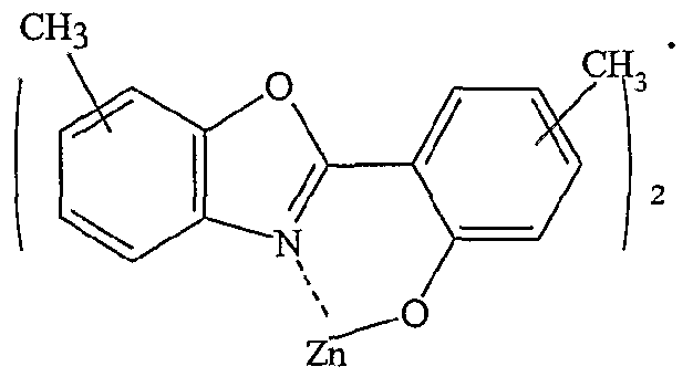
Also included within the scope of the present invention are benzoxazole host compounds having the chemical formula (herein referred to as "metal(BOX)" compounds):
Figure imgf000017_0002
where X and Y are independently O, S;
M represents a metal; n is a integer from 1 to 3; and
R, to R8 are, independently, a hydrogen atom, an aryl group or an alkyl group.
As used herein, the term "BOX" is used to encompass any benzoxazole compound or derivative as depicted above. Alkyl groups of length one to four carbons are preferred alkyl chain lengths.
Preferred embodiments are have a chemical formula within the following class of compounds:
Figure imgf000018_0001
In this representation, the line segments to the CH3- (methyl-) group denote substitution at any allowed ring position by each methyl independently. Specific preferred embodiments are compounds having the following chemical structures (Zn(BOX-DMe)2):
Figure imgf000018_0002
and
Figure imgf000019_0001
These are methyl-substituted bis(2-(2-hydroxyphenyl)-benzoxazolate)zinc derivatives. Preferred embodiments are also within the following class:
Figure imgf000019_0002
and
Figure imgf000019_0003
These are methyl-substituted as well as un-substituted bis(2-(2-hydroxyphenyl)- benzthiazolate)zinc derivatives.
These benzoxazole and benzthiazole host compounds are exemplified for the metal Zn. Useful results may also be expected for phosphorescent-doped Os, Ir, and Pt host benzoxazole and benzthiazole host compounds and analogous derivatives for which the excited triplet state of the host benzoxazole compound is of higher energy than the emissive triplet state of the phosphorescent dopant material.
The use of a first electron transporting layer that is doped with a electrophosphorescent material can improve the electrophosphorescent efficiency as compared with devices in which the electrophosphorescent material is doped in a hole transporting material. Since the electrophosphorescent emission occurs in the emissive layer (EML) within close proximity to the HTL/EML interface, the EML layer is preferably a very thin layer as compared with the HTL or second ETL. For example, the EML preferably has a thickness of about 2.5 nm to about 30 nm whereas the HTL and ETL typically have a thickness of about 5 nm to about 60 nm. More preferably, the EML has a thickness of about 5 nm to about 25 nm.
The first electron transporting layer, which is the emissive layer (EML), may include any suitable host material that acts as a good transporter of charge and also efficiently transfers energy to a highly luminescent guest. In the preferred embodiments, the first electron transporting layer is a host material of 3-phenyl-4-(l'-naphthyl)-5-phenyl-l,2,4- triazole (TAZ), an oxadiazole or an oxadiazole derivative such as OXD-7, as depicted herein, or a phenanthroline such as 2,9-dimethyl-4,7-diphenyl-l,10-phenanthroline (bathocuproine or BCP) a BCP derivative, or a substituted or un-substituted benzoxazole or benzthiazole compound. These thin films possess good electron transport characteristics while also serving to block hole and exciton transport. BCP has the following formula:
Figure imgf000021_0001
The first electron transporting layer, preferably TAZ, OXD-7, BCP or a benzoxazole or benzthiazole compound may function as an electron transport layer and or as an exciton blocking layer. The exciton blocking layer in OLED devices substantially blocks the diffusion of excitons, thus substantially keeping the excitons within the first ETL to enhance device efficiency. The phosphorescent dopants of the present invention are believed to trap excitons within the luminescent region, thus improving the efficiency of devices of the present invention over other devices. In particular, using TAZ as the host and Ir(ppy)3 as the dopant, a maximum external quantum efficiency of 15.4% and power luminous efficiency of 40 lm/W may be achieved. The electroluminescent spectra due to an Ir(ppy)3 triplet are independent of ETL host thickness. Thus, it is believed that the electroluminescence may be due to trapping of charge carriers and efficient formation of radiative triplet excitons on theJr(ppy)3 dopant. The charge carriers and triplet excitons are believed to be confined within the very thin EML.
A material that is used as the exciton blocking layer in an OLED may be defined as a material that has an exciton energy, defined as the energy difference between the election and hole in a ground state exciton, that is greater than the energy of the excitons that are produced in the emissive layer of the OLED. Because of the coulomb forces between the nearby electron and hole in a ground state exciton, the exciton energy of an organic material is typically slightly less than the energy difference between the lowest unoccupied molecular orbital (LUMO) and the highest occupied molecular orbital (HOMO) of the material. Such an exciton energy substantially prevents the diffusion of excitons through the blocking layer, yet has only a minimal effect on the turn-on voltage of a completed electroluminescent device. Phosphorescent emitters having satisfactory characteristics, such as stability, luminance, weather resistance and afterglow, maybe used as phosphorescent dopants in the present invention. Specific examples of phosphorescent molecules include organometallic complexes of metal species M with a bidentate mono-anionic ligand in which M is coordinated with an sp2 hybridized carbon and a heteroatom of the ligand. The complex may be of the form L3M (wherein each ligand L species is the same), L L' L" M (wherein each ligand species L, If, L" is distinct), or L2MX, wherein X is a monoanionic bidentate ligand. It is generally expected that the ligand L participates more in the emission process than does X. Preferably, M is a third row transition metal and most preferably M is Ir or Pt. Such molecules also include meridianal isomers of L3M wherein the heteroatoms (such as nitrogen) of two ligands L are in a trans configuration. In an embodiment in which M is coordinated with an sp2 hybridized carbon and a heteroatom of the ligand, it is preferred that the ring comprising the metal M, the sp2 hybridized carbon and the heteroatom contain 5 or 6 atoms.
In phosphorescent molecules having the formula L2MX, L and X are distinct bidentate ligands and M is a metal of atomic number greater than 40 which forms octahedral complexes and is preferably a member of the third row (of the transition series of the periodic table) transition metals, preferably iridium (Ir). A preferred embodiment is a compound of formula L2IrX, wherein L and X are distinct bidentate ligands, as a dopant in a host electron transporting layer in an organic light emitting device. Alternatively, M can be a member of the second row transition metals, or of the main group metals, such as Zr and Sb. Some of such organometallic complexes electroluminesce, with emission coming from the lowest energy ligand or metal ligand charge transfer ("MLCT") state. L coordinates to M via atoms of L comprising sp2 hybridized carbon and heteroatoms.
The above phosphorescent emitter molecules having the formula L2MX can be made by the direct reaction of chloride bridged dimers of the form L2M(μ-Cl)2ML2, wherein L a bidentate ligand, and M a metal such as Jr, with species XH which serve to introduce a bidentate ligand X. XH can be, for example, acetylacetone, 2-picolinic acid, or N- methylsalicyclanilide, and H stands for hydrogen. The resultant product is of formula L2MX, wherein one can have an octahedral disposition of the bidentate ligands L, L, and X about M.
The resultant compounds of formula L2MX can be used as phosphorescent emitters in organic light emitting devices. For example, compounds having the formula L2MX, wherein L=(2-phenylbenzothiazole), X=acetylacetonate, and M=Ir (the compound abbreviated as BTIr) may be used phosphorescent emitters when used as a dopant. The synthetic process to make L2MX may be used advantageously in a situation in which L, by itself, is fluorescent, but the resultant L2MX is phosphorescent. One specific example of this is where L=coumarin-6. L2IrX has been prepared wherein L=coumarin and X=acac. This compound is referred to as coumarin-6 ["C61f"]. The complex gives intense orange emission, whereas coumarin by itself emits green.
If the L ligand that is used in making the L2MX (for example, M=Ir) complex has a high fluorescent quantum efficiency, it is possible to use the strong spin orbit coupling of the Ir metal to efficiently intersystem cross in and out of the triplet states of the ligands. Ir makes the L ligand an efficient phosphorescent center. Using this approach, it is possible to take substantially any fluorescent dye and make an efficient phosphorescent molecule from it (that is, L fluorescent but E,MX (M=Ir) phosphorescent).
The appropriate selection of L and X allows color tuning of the complex L2MX relative to L3M. For example, Ir(ppy)3 and (ppy)2Ir(acac) both give strong green emission with a λmax of 510 nm [ppy denotes phenyl pyridine] . However, if the X ligand is formed from picolinic acid instead of from acetylacetone, there is a small blue shift of about 15 nm.
Non-limiting examples of L are 2-(l-naphthyl)benzoxazole), (2-phenylbenzoxazole), (2-phenylbenzothiazole), (2-phenylbenzothiazole), (7,8-benzoquinoline), coumarin, (thienylpyridine), phenylpyridine, benzothienylpyridine, 3-methoxy-2-phenylpyridine, thienylpyridine, and tolylpyridine.
Non-limiting examples of X are acetylacetonate ("acac"), hexafluoroacetylacetonate, salicylidene, picolinate, and 8-hydroxyquinolinate.
Further examples of L and X may be found in Comprehensive Coordination Chemistry, Volume 2, G. Wilkinson (editor-in-chief), Pergamon Press, especially in chapter 20.1 (beginning at page 715) by M. Calligaris and L. Randaccio and in chapter 20.4 (beginning at page 793) by R. S. Vagg.
Furthermore, X can be selected such that it has a certain HOMO level relative to the L3M complex so that carriers (holes or electrons) might be trapped on X (or on L) without a deterioration of emission quality. In this way, carriers (holes or electrons) which might otherwise contribute to deleterious oxidation or reduction of the phosphor would be impeded. The carrier that is remotely trapped could readily recombine with the opposite carrier either intramolecularly or with the carrier from an adjacent molecule.
Other phosphorescent emitter molecules that may be used have the formula L L' L" M, wherein L, L', and L" are the same or different, wherein L, L', and L" are bidentate, monoanionic ligands, wherein M is a metal which forms octahedral complexes, preferably a member of the third row of transition metals, more preferably Ir or Pt, and wherein the coordinating atoms of the ligands comprise sp2 hybridized carbon and a heteroatom. Certain phosphorescent compounds have been studied wherein M = iridium. The resultant iridium complexes emit strongly, in most cases with lifetimes of 1-3 microseconds ("μsec"). Such a lifetime is indicative of phosphorescence. The radiative transition in these materials is from a metal ligand charge transfer complex (MLCT).
To understand the specific phosphorescent molecules described herein it is useful to discuss the underlying mechanistic theory of energy transfer. There are two mechanisms commonly discussed for the transfer of energy to an acceptor molecule, fn the first mechanism of Dexter transport (D.L. Dexter, "A theory of sensitized luminescence in solids," J. Chem. Phys., 1953, 21, 836-850), the exciton may hop directly from one molecule to the next. This is a short-range process dependent on the overlap of molecular orbitals of neighboring molecules. It also preserves the symmetry of the donor and acceptor pair (E. Wigner and E.W. Wittmer, Uber die Struktur der zweiatomigen Molekelspektren nach der Quantenmechanik, Zeitschrift fur Physik, 1928, 51, 859-886; M. Klessinger and J. Michl, Excited states and photochemistry of organic molecules (VCH Publishers, New York, 1995). Thus, the energy transfer of Eq. (1) is not possible via Dexter mechanism. In the second mechanism of Fδrster transfer ( T. Fδrster, Zwischenmolekulare Energiewanderung and Fluoreszenz, Annalen der Physik, 1948, 2, 55-75; T. Fδrster, Fluoreszenz organischer Verbindugen (Vandenhoek and Ruprecht, Gottinghen, 1951 ), the energy transfer of Eq. (1) is possible. In Fδrster transfer, similar to a transmitter and an antenna, dipoles on the donor and acceptor molecules couple and energy may be transferred. Dipoles are generated from allowed transitions in both donor and acceptor molecules. This typically restricts the Fόrster mechanism to transfers between singlet states.
Nevertheless, as long as the phosphor can emit light due to some perturbation of the state such as due to spin-orbit coupling introduced by a heavy metal atom, it may participate as the donor in Fόrster transfer. The efficiency of the process is determined by the luminescent efficiency of the phosphor (F Wilkinson, in Advances in Photochemistry (eds. W.A. Noyes, G. Hammond, and J.N. Pitts), pp. 241-268, John Wiley & Sons, New York, 1964), i.e., if a radiative transition is more probable than a non-radiative decay, then energy transfer will be efficient. Such triplet-singlet transfers were predicted by Fόrster (T. Fόrster, "Transfer mechanisms of electronic excitation," Discussions of the Faraday Society, 1959, 27, 7-17) and confirmed by Ermolaev and Sveshnikova (V.L. Ermolaev and E. B. Sveshnikova, "Inductive-resonance transfer of energy from aromatic molecules in the triplet state," Doklady AkademiiNaukSSSR, 1963, 149, 1295-1298), who detected the energy transfer using a range of phosphorescent donors and fluorescent acceptors in rigid media at 77K or 90K. Large transfer distances are observed; for example, with triphenylamine as the donor and chrysoidine as the acceptor, the interaction range is 52 A.
The remaining condition for Fόrster transfer is that the absorption spectrum should overlap the emission spectrum of the donor assuming the energy levels between the excited and ground state molecular pair are in resonance.
Devices whose structure is based upon the use of layers of organic optoelectronic materials generally rely on a common mechanism leading to optical emission. Typically, this mechanism is based upon the radiative recombination of a trapped charge. Specifically, OLEDs are comprised of at least two thin organic layers separating the anode and cathode of the device. The material of one of these layers is specifically chosen based on the material's ability to transport holes, a "hole transporting layer" (HTL), and the material of the other layer is specifically selected according to its ability to transport electrons, an "electron transporting layer" (ETL). With such a construction, the device can be viewed as a diode with a forward bias when the potential applied to the anode is higher than the potential applied to the cathode. Under these bias conditions, the anode injects holes (positive charge carriers) into the hole transporting layer, while the cathode injects electrons into the electron transporting layer. The portion of the luminescent medium adjacent to the anode thus forms a hole injecting and transporting zone while the portion of the luminescent medium adjacent to the cathode forms an electron injecting and transporting zone. The injected holes and electrons each migrate toward the oppositely charged electrode. When an electron and hole localize on the same molecule, a Frenkel exciton is formed. Recombination of this short-lived state may be visualized as an electron dropping from its conduction potential to a valence band, with relaxation occurring, under certain conditions, preferentially via aphotoemissive mechanism. Under this view of the mechanism of operation of typical thin-layer organic devices, the electroluminescent layer comprises a luminescence zone receiving mobile charge carriers (electrons and holes) from each electrode. The OLEDs of the present invention include two electron transporting layers. The electron transporting layer adjacent to the hole transporting layer contains phosphorescent molecules doped therein.
As noted above, light emission from OLEDs is typically via fluorescence or phosphorescence. It has been noted that phosphorescent efficiency can decrease rapidly at high current densities. It may be that long phosphorescent lifetimes cause saturation of emissive sites, and triplet-triplet annihilation may also produce efficiency losses. Another difference between fluorescence and phosphorescence is that energy transfer of triplets from a conductive host to a luminescent guest molecule is typically slower than that of singlets; the long range dipole-dipole coupling (Fδrster transfer) which dominates energy transfer of singlets is (theoretically) forbidden for triplets by the principle of spin symmetry conservation. Thus, for triplets, energy transfer typically occurs by diffusion of excitons to neighboring molecules (Dexter transfer); significant overlap of donor and acceptor excitonic wavefunctions is critical to energy transfer. Another distinction between singlets and triplets is that triplet diffusion lengths are typically long (e.g., >1400A) compared with typical singlet diffusion lengths of about 200 A. Thus, if phosphorescent devices are to achieve their potential, device structures need to be optimized for triplet properties. In the phosphorescent molecules having one formula L2MX or L L' L"M, the property of long triplet diffusion lengths may be exploited to improve external quantum efficiency. Whenever a dopant is present in one of the organic layers, the predominant material in the charge carrier layer is refened to as a host compound. Materials that are present as host and dopant are selected so as to have a high level of energy transfer from the host to the dopant material. In addition, these materials need to be capable of producing acceptable electrical properties for the OLED. Furthermore, such host and dopant materials are preferably capable of being incorporated into the OLED using materials that can be readily incorporated into the OLED by using convenient fabrication techniques, in particular, by using vacuum-deposition techniques.
As found in the IrL3 system described above, the emission color is strongly affected by the L ligand. This is consistent with the emission involving either MLCT or intraligand transitions. In all of the cases made in both the tris complex (i.e., IrL3) and the L2IrX complex, the emission spectra are very similar. For example h(ρpy)3 and (ppy)2Ir(acac) (PPIr) give strong green emission with a λmax of 510 nm.
However, in other cases, the choice of X ligand affects both the energy of emission and efficiency. Acac and salicylanilide L2IrX complexes give very similar spectra. The picolinic acid derivatives that have been prepared typically show a small blue shift (15 nm) in their emission spectra relative to the acac and salicylanilide complexes of the same ligands.
If an X ligand is used whose triplet levels fall lower in energy than the "L2Ir" framework, emission from the X ligand can be observed. The phosphorescence spectra for heavymetal quinolates (e.g. IrQ3 or PtQ2) are centered at 650 nm. The complexes themselves emit with very low efficiency, < 0.01. Both the energy and efficiency of the L2IrQ material is consistent "X" based emission. If the emission form the X ligand or the "IrX" system were efficient this could have been a good red emitter. It is important to note that while all of the examples list here are strong "L" emitters, this does not preclude a good phosphor from being formed from "X" based emission.
Preferably, in the embodiments of the present invention having first and second electron transporting layers, the second electron transporting layer may be made of the electron transport material tris-(8-hydroxyquinoline)aluminum (Alq3), which is used to transport electrons into the first electron transporting layer. Other suitable ETL materials that may be used as the second electron transporting layer can be found in U.S. Patent No. 5,707,745, which, as indicated above, is incorporated in its entirety herein by reference. The Alq3, which functions as an electron injection/electron transport layer has the following formula:
Figure imgf000030_0001
The second electron transporting layer is preferably from about 50 A to about 200 A thick.
Preferably, at least one of the hole transporting layer and the first and second electron transporting layers is vapor deposited. More preferably, each of these layers is vapor deposited. Other deposition techniques may be used and are known to those skilled in the art.
In the OLED structures of the present invention, light may be emitted from the substrate side of the device, or alternatively, from the side of the device opposite the substrate, that is, as a top emitting device.
The present invention also encompasses stacked OLED structures, in which at least one OLED or inverted OLED having a doped first ETL between an HTL and a second ETL, is stacked over a substrate. When more than one OLED is stacked over the substrate, the OLEDs are stacked one upon the other. An embodiment of a stacked OLED structure according to the present invention includes a substrate, a first organic light emitting device over the substrate, and a second organic light emitting device stacked over the first organic light emitting device. In another embodiment of the stacked OLED structure, a third organic light emitting device is stacked over the second organic light emitting device. In these structures at least one of the OLEDs has one of the following structures: 1) anode, hole transporting layer over the anode, first electron transporting layer (doped with a phosphorescent material) over the hole transporting layer, second electron transporting layer over the first electron transporting layer, and a cathode over the second electron transporting layer, or 2) a cathode, a first electron transporting layer over the cathode, a second electron transporting layer (doped with a phosphorescent material) over the first electron transporting layer, a hole transporting layer over the second electron transporting layer, and an anode over the hole transporting layer.
Also encompassed within the present invention are methods of fabricating organic light emitting device structures, which include depositing the layers of each OLED one over the other to form organic light emitting device structures. In embodiments having only one OLED over a substrate, one embodiment of the method includes forming a first electrically conductive (anode) layer over a substrate; depositing a first hole transporting layer over the first conductive layer; depositing a first electron transporting layer over the first hole transporting layer, wherein the first electron tiansporting layer is doped with a phosphorescent material; depositing a second electron transporting layer over the first electron transporting layer; and depositing a second electrically conductive (cathode) layer over the first election tiansporting layer. Alternatively, in inverted OLED embodiments, the layers may be deposited starting with the second electrically conductive (cathode) layer and ending with the first electrically conductive (anode) layer.
OLEDs fabricated in accordance with the above embodiment may contain for example, an ITO layer, a TPD layer thereover having a thickness of approximately 50 nm, an oxadiazole layer (OXD-7, as depicted above) doped, for example, with lr(ppy)3 (8.8%) having a thickness of approximately 20 nm, an Alq3 layer thereover of approximately 40 nm thickness, and an MgAg layer thereover. A depiction of the EL intensity achievable by such an embodiment as a function of wavelength of this embodiment is depicted in Figure 1. A depiction of the quantum efficiency as a function of current density is depicted in Figure 2. The ITO coated substrate maybe exposed to an ultra-violet/ozone treatment before deposition of the organic layers, with such a electrode/substrate layer being identified as an "ITO(UN)" electrode/substrate layer.
Substrates according to the present invention may be opaque or substantially transparent, rigid or flexible, and/or plastic, metal or glass. Although not limited to the thickness ranges recited herein, the substrate maybe as thin as 10 μm if present as a flexible plastic or metal foil substrate, or substantially thicker if present as a rigid, transparent or opaque substrate, or if the substiate is made of silicon.
Suitable electrode (i.e., anode and cathode) materials include conductive materials such as a metal, a metal alloy or ITO which form electrical contacts. The deposition of electrical contacts may be accomplished by vapor deposition or other suitable metal deposition techniques. These electrical contacts may be made, for example, from indium, magnesium, platinum, gold, silver or combinations such as Ti Pt/Au, Cr/Au or Mg/Ag.
When depositing the top electrode layer (i.e., the cathode or the anode, typically the cathode), that is, the electrode on the side of the OLED furthest from the substrate, damage to the organic layers should be avoided. For example, organic layers should not be heated above their glass transition temperature. Top electrodes are preferably deposited from a direction substantially perpendicular to the substrate.
In preferred embodiments, the cathode is preferably a low work function, electron- inj ecting material, such as a metal layer. Preferably, the cathode material has a work function that is less than about 4 electron volts. The cathode preferably is a metal layer of about 100 A (angstroms) thick or less, and maybe about 50 A thick or less. The contacts are preferably made of magnesium silver or a magnesium and silver alloy. The metal cathode layer may be substantially thicker if the cathode layer is opaque. The anode is preferably a high work function hole-injecting metal anode layer, for example, an indium tin oxide (ITO) layer. ITO is a transparent conductor which functions as an anode. ITO is a degenerate semiconductor formed by doping a wide band semiconductor. The carrier concentration of the ITO is in excess of 1019/cm3. The ITO anode layer maybe about 500 Λ to greater than about 4000 A thick.
In one preferred embodiment, the hole transporting layer is 4,4'-bis[N,N'-(3- tolyl)amino]-3,3'-dimethylbiphenyl (HMTPD). The hole transporting layer is preferably about 100 Λ to about 800 A thick, even more preferably about 200 A to about 700 Λ thick, and most preferably about 600 Λ thick. Other examples of materials that may be suitable materials for the hole transporting layer can be found in U.S. Patent No. 5,707,745, which is incorporated herein in its entirety by reference. Other materials suitable for use as a hole transporting layer may include, for example, 4,4'-bis[N-(l~naphthyl)- V-phenyl- aminojbiphenyl ( -ΝPD); Ν,Ν'-diphenyl-Ν,Ν'-bis(3-methylpheny) 1-1 'biphenyl-4,4'diamine (TPD); 4,4'-bis[N,N'-(3-tolyl)amino]-3,3'-dimethylbiphenyl (M14); and 4,4',4"-tris(30methylphenylphenylamino)triphenylamine (MTDATA). Other suitable hole tiansporting materials are known in the art.
The present invention may also be used to fabricate transparent OLED structures. A device that is transparent is well suited for use in a heads-up display, for example on a windshield for a car, or a visor for a motorcycle or airplane helmet. Transparent OLED devices can also be stacked for multi-color products or to enhance intensity. In this embodiment, all layers should be transparent to visible light in a transparent OLED. A device that is transparent is also well suited for high contrast applications. High contrast is achieved by placing a background made of an optically absorbent material next to the display device. Light incident upon the device from external sources passes through the device and is absorbed by the background, reducing the reflection of light from external sources to the viewer.
It is desirable for the OLEDs of the present invention to be fabricated using materials that provide electroluminescent emission in a relatively narrow band centered near selected spectral regions, which correspond to one of the three primary colors, red, green and blue so that they may be used as a colored layer in an OLED or SOLED. It is also desirable that such compounds be capable of being readily deposited as a thin layer using vacuum deposition techniques so that they may be readily incorporated into an OLED that is prepared entirely from vacuum-deposited organic materials.
The OLEDs and OLED structures of the present invention optionally contain additional materials or layers depending on the desired effect, such as protective layers (to protect certain materials during the fabrication process), insulating layers, reflective layers to guide waves in certain directions, and protective caps, which cover the electrodes and organic layers in order to protect these layers from the environment. A description of insulating layers and protective caps is contained for example, in U.S. Patent No. 6,013,538, which is hereby incorporated by reference.
There may be substantial variation of the type, number, thickness and order of the layers that are present, dependent on whether the device is a stacked OLED or a single OLED, whether an inverted sequence of OLED layers is present, whether the OLED is intended to produce emission in a preferred spectral region, or whether still other design variations are used. This invention will now be described in detail with respect to showing how a certain specific representative embodiment thereof can be made, the materials, apparatus and process steps being understood as examples that are intended to be illustrative only. In particular, the invention is not intended to be limited to the methods, materials, conditions, process parameters, apparatus and the like specifically recited herein.
EXAMPLES OF THE INVENTION
Example 1:
A first HTL is first deposited onto the ITO (indium tin oxide) coated glass substrate. The first HTL consists of 400 A of R854. A second HTL, which is also a blocking layer, consisting of TAZ, having a thickness of about 20 nm (200 A) is deposited onto the HTL layer. The first electron transporting layer is doped with Tr(ppy)3. A second electron transport layer of Alq3 having a thickness of about 20nm is deposited onto the first electron transporting layer. The device is finished by depositing a Mg-Ag electrode onto the second electron transporting layer. This Mg-Ag electrode has of thickness 100 nm. All of the depositions are carried out at a vacuum less than 5 X 10"5 Torr. The devices are tested in air, without packaging.
When a voltage is applied between the cathode and the anode, holes are injected from ITO to NPD and transported by the NPD layer, while electrons are injected from MgAg to Alq3 and transported through Alq3. Then holes and electrons are injected into the first electron transporting layer and carrier recombination occurs in BCP, the excited states were formed, and the dopant molecules are excited and decay radiatively. Example 2:
Organic layers were deposited by high vacuum (10"6 Torr) thermal evaporation onto a clean glass substrate precoated with an ITO layer. A 60 nm-thick film of 4,4'-bis[N,N'-(3- tolyl)amino]-3,3'-dimethylbiphenyl QTMTPD) serves as the HTL. Next a 25 nm-thick EML consisting of 6% to 8% Ir(ppy)3 is doped into various election transporting hosts via thermal co-deposition. A 50 nm-thick layer of the electron transport material tris-(8- hydroxyquinoline)aluminum (Alq3) is used to transport and inject electrons into the EML. A shadow mask with 1 mm-diameter openings was used to define the cathode consisting of a 150nm-thick magnesium silver (Mg-Ag) layer, with a 20 nm-thick Ag cap. Alternatively, the cathode consisted of a 100 nm-thick layer of aluminum-0.56wt% lithium.
Current density (J) versus voltage (V) measurements were obtained using a semiconductor parameter analyzer, with the luminance (L) obtained by placing the OLEDs directly onto the surface of a calibrated silicon photodiode. The photoluminescence lifetime was characterized using a stieak camera following excitation by a nitrogen laser at a wavelength of 337 nm and a pulse width of 500 ps.
Figure 3 shows the external quantum (η) and power efficiencies of a 7%-Ir(ppy)3 doped TAZ device using an Al-Li cathode. A maximum η=15.4 ± 0.2% and power efficiency of 40 lm/W were obtained, corresponding to an internal quantum efficiency of 77%. Furthennore, a high optical output power of P=2.5mW/cm2 (corresponding to a luminance of about 4000cdVm2) with η=10% was maintained even at J=10mA/cm2. The device exhibits a very gradual decrease in quantum efficiency with increasing current characteristic of triplet-triplet annihilation effects observed in all electrophosphorescent devices. The value of η is improved over known devices. At Ir(ρpy)3 concentrations less than 2%, a decrease to η of about 3% was observed along with additional blue host emission (wavelength about 440 nm), while at high Ir(ppy)3 concentrations, a significant decrease in η was also observed due to the aggregate induced quenching.
In Table 1 below the performance of Ir(ppy)3 doped OLEDs with various hosts and cathode metals is summarized. Table 1
Host cathode η(%) at J 1 (mA/cm2) photo luminescent
0.1 1 10 100 decay time τ(ns)
TAZ AlLi 15.4 12.9 10.0 6.3 about 650
MgAg 12.3 11.9 9.7 5.8 about 650
OXD7 MgAg 11.6 11.9 8.9 4.4 about 650
BCP MgAg 9.6 8.3 6.3 3.8 about 380
As shown in Figure 4, the transient phosphorescent time decay of h(ppy)3 in TAZ or OXD-7 is about 650 ns, compared with a measured lifetime of about 380 ns in 7%- Ir(ppy)3:BCP at room temperature. Since the phosphorescence efficiency is approximately proportional to the phosphorescent lifetime, the longer lifetime in TAZ and OXD7 accounts for the higher EL efficiencies of these devices.
In several experiments, the EML thickness was varied from 30 nm to 2.5 nm while maintaining both the HTL and ETL thicknesses at 50 nm and 40nm, respectively. These devices were compared with a double heterostructure comprised of an EML sandwiched between HMTPD and a lOnm thick ETL, as shown in the inset of Figure 5. Figure 5 shows the thickness dependence of η at a fixed current density of 0. lmA cm2 for both single heterostructure and double heterostructure devices using BCP as a host. At an EML thickness of less than 15 nm, a significant decrease of η was observed in the SH device, while a high η=9% was retained even with a 2.5nm-thick EML in the DH device. This suggests the successful confinement of both charge carriers and triplet excitons within the thin EML.
In Figure 6, the EL spectra of two SH devices with an EML thickness of 2.5nm and 30nm are shown, as well as that of an ITO/HMTPD/Alq3/MgAg device. Also, the dependence of the full width at half maximum (FWHM) of the EL spectra on the EML thickness in the SH devices, is plotted. It is believed from Figure 6 that the exciton formation occurs entirely in the EML, followed by direct charge trapping by fr(ppy)3. Since BCP serves as both an electron transporting and hole blocking material, holes are directly injected from the HTL into the Ir(ppy)3 highest occupied molecular orbital level, and subsequently recombine with electrons which are transported across the BCP layer, leading to triplet formation in the Ir(ppy)3.
External EL efficiencies of electrophosphorescent devices as high as 15.4%, conesponding to an internal efficiency approaching 80% may be achieved by the present invention. Furthermore, luminance efficiency of 40 lm W may be obtained using 7% Ir(ppy)3:TAZ.
The external quantum efficiencies are also shown as a function of cureent density for an OLED having Ir(ppy)3 doped in a phenanthroline (BCP) host material, Figure 8; doped in a triazole (TAZ) host material, Figure 9; doped in a zinc benzoxazole (Zn(BOX-DMe2) host material, Figure 10 ; and doped in a 4,4'-N,N'-dicarbazole-biphenyl (CBP) host material, Figure 7. Devices that include the benzoxazole (Zn(BOX-DMe2) and 4,4'-N,N'-dicarbazole- biphenyl (CBP) compounds maybe fabricated using similar fabrication methods.
The structures of the present invention maybe used for example, in substantially any type of device that includes one or more OLEDs including billboards and signs, computer monitors, vehicles, telecommunications devices, telephones, printers televisions, large area wall screens, theater screens and stadium screens.
While the present invention is described with respect to particular examples and prefened embodiments, it is understood that the present invention is not limited to these examples and embodiments. In particular, the present invention may be applied to a wide variety of electronic devices. The present invention as claimed therefore includes variations from the particular examples and prefened embodiments described herein, as will be apparent to one of skill in the art.

Claims

WHAT IS CLAIMED IS:
1. A device for producing electroluminescence comprising an organic light emitting device including an emissive layer comprising a charge carrying host material doped with a phosphorescent material having a triplet excited state with a triplet energy that is less than the triplet state energy of the lowest triplet excited state of the charge carrying host material.
2. The device of claim 1 wherein the triplet excited state of the phosphorescent dopant material has a triplet energy that is at least 0.1 eV less than the triplet state energy of the lowest triplet excited state of the charge carrying host material.
3. The device of claim 1 wherein the charge carrying host material comprises an electron transporting host material.
4. The device of claim 3 wherein the phosphorescent dopant material has a HOMO energy less than the ionization potential of the electron transporting host material.
5. The device of claim 3 wherein the phosphorescent dopant material has a LUMO energy level lower than the LUMO energy level of the electron transporting host material.
6. The device of claim 3 wherein the electron transporting host material is selected from the group consisting of an aryl-substituted oxadiazole, an aryl-substituted triazole and an aryl-substituted phenanthroline.
7. The device of claim 6 wherein the aryl-substitated oxadiazole comprises 1,3-bis (N,N-t-butyl-phenyl)-l,3,4-oxadiazole.
8. The device of claim 6 wherein the aryl-substituted triazole comprises 3-phenyl- 4-(l '-naphthyl)-5-phenyl- 1 ,2,4-triazole.
9. The device of claim 6 wherein the aryl-substitated phenanthroline comprises 2,9-dimethyl-4,7-diphenyl-l,10-phenanthroline.
10. The device of claim 3 wherein the electron transporting material comprises a benzoxazole or benzthiazole compound having the chemical structure:
Figure imgf000042_0001
where X and Y are independently O, S;
M represents a metal; n is a integer from 1 to 3; and
Rj to R8 are, independently, a hydrogen atom, an aryl group or an alkyl group.
11. The device of claim 3 wherein the electron transporting material comprises a zinc benzoxazole compound having the chemical structure:
Figure imgf000043_0001
12. The device of claim 3 wherein the electron transporting material comprises a zinc benzoxazole compound having the chemical structure:
Figure imgf000043_0002
13. The device of claim 1 wherein the phosphorescent dopant material comprises fac-tris (2-phenylpyridine)-iridium.
14. An organic light emitting device comprising: a substrate; an anode layer over said substrate; a hole transporting layer over said anode layer; a first electron transporting layer over said hole transporting layer, wherein said first election transporting layer comprises an electron transporting host material doped with a phosphorescent dopant material having an emissive triplet excited state; a second election transporting layer over said first electron transporting layer; and a cathode layer over said second electron transporting layer; wherein said electron tiansporting host material has a lowest triplet excited state that is of higher energy than the emissive triplet excited state of said phosphorescent dopant material.
15. The organic light emitting device of claim 14 wherein said second electron transporting layer is comprised of a material having an ionization potential at least 0.1 eV higher than the ionization potential of said electron transporting host material.
16. The organic light emitting device of claim 14 wherein said lowest triplet excited state is of at least 0.1 eV higher energy than said emissive triplet excited state of said phosphorescent dopant material.
17. The organic light emitting device of claim 14 wherein the said phosphorescent dopant material has a HOMO energy that is less than the ionization potential of the electron transporting host material.
18. The organic light emitting device of claim 14 wherein the phosphorescent dopant material has a LUMO energy level lower than the LUMO energy level of the electron transporting host material.
19. The organic light emitting device of claim 14 wherein said electron transporting host material is selected from the group consisting of an aryl-substitated oxadiazole, an aryl- substituted triazole and an aryl-substituted phenanthroline.
20. The organic light emitting device of claim 19 wherein the aryl-substitated oxadiazole comprises 1,3-bis (N,N-t-butyl-phenyl)-l,3,4-oxadiazole.
21. The organic light emitting device of claim 19 wherein the aryl-substituted triazole comprises 3-phenyl-4-(l '-naphthyl)-5-phenyl-l,2,4-triazole.
22. The organic light emitting device of claim 19 wherein the aryl-substituted phenanthroline comprises 2,9-dimethyl-4,7-diphenyl- 1 , 10-phenanthroline.
23. The organic light emitting device of claim 14 wherein said electron transporting host material comprises a benzoxazole or benzthiazole compound having the chemical structure:
Figure imgf000045_0001
where X and Y are independently O, S;
M represents a metal; n is a integer from 1 to 3; and
R] to Rg are, independently, a hydrogen atom, an aryl group or an alkyl group.
24. The organic light emitting device of claim 14 wherein said electron transporting host material comprises a zinc benzoxazole compound having the chemical structure:
Figure imgf000046_0001
25. The organic light emitting device of claim 14 wherein said electron transporting host material comprises a zinc benzoxazole compound having the chemical structure:
26. The organic light emitting device of claim 14 wherein said first phosphorescent dopant material comprises fac-tris (2-phenylpyridine)-iridium.
27. An organic light emitting device comprising: a substrate; an anode layer over said substrate; a hole transporting layer over said anode layer; an electron transporting layer over said hole transporting layer, wherein said electron transporting layer comprises an electron transporting host material doped with a phosphorescent dopant material having an emissive triplet excited state; and a cathode layer over said electron transporting layer; wherein said electron transporting host material has a lowest triplet excited state that is of higher energy than the emissive triplet excited state of said phosphorescent dopant material.
28. The organic light emitting device of claim 27 wherein said electron tiansporting host material has a lowest triplet excited state with an energy level that is at least 0.1 eV higher than the emissive triplet excited state of said phosphorescent dopant material.
29. The organic light emitting device of claim 27 wherein the phosphorescent dopant material has a HOMO energy less than the ionization potential of the electron transporting host material.
30. The organic light emitting device of claim 27 wherein the phosphorescent dopant material has a LUMO energy level lower than the LUMO energy level of the electron transporting host material.
31. An inverted organic light emitting device comprising: a substrate; a cathode layer over said substrate; a first electron transporting layer over said cathode layer; a second electron transporting layer over said first transporting layer, wherein said second election transporting layer comprises an electron transporting host material doped with a phosphorescent dopant material having an emissive triplet excited state; and a hole transporting layer over said second election transporting layer; and an anode layer over said second electron transporting layer; wherein said electron transporting host material has a lowest triplet excited state that is of higher energy than the emissive triplet excited state of said phosphorescent dopant material.
32. The inverted organic light emitting device of claim 31 wherein said electron transporting host material has a lowest triplet excited state with an energy level that is at least 0.1 eV higher than the emissive triplet excited state of said phosphorescent dopant material.
33. The inverted organic light emitting device of claim 31 wherein the phosphorescent dopant material has a HOMO energy less than the ionization potential of the electron transporting host material.
34. The inverted organic light emitting device of claim 31 wherein the phosphorescent dopant material has a LUMO energy level lower than the LUMO energy level of the electron transporting host material.
35. A method of fabricating an organic light emitting device comprising: fonning an anode layer over a substrate; depositing a hole transporting layer over said anode layer; selecting an electron transporting host material and a phosphorescent dopant material, wherein said electron transporting host material has a lowest triplet excited state that is of higher energy than the emissive triplet excited state of said phosphorescent dopant material; depositing said electron transporting host material together with said phosphorescent dopant material over said hole transporting layer, so as to produce a first electron transporting layer comprising the electron transporting host material doped with the phosphorescent dopant material; depositing a second electron transporting layer over said first electron transporting layer; and depositing a cathode layer upon said first electron transporting layer.
36. The method of claim 35 wherein said electron transporting host material has a lowest triplet excited state with an energy level that is at least 0.1 eV higher than the emissive triplet excited state of said phosphorescent dopant material.
37. The method of claim 35 wherein the phosphorescent dopant material has a HOMO energy less than the ionization potential of the electron transporting host material.
38. The method of claim 35 wherein the phosphorescent dopant material has a LUMO energy level lower than the LUMO energy level of the electron tiansporting host material.
PCT/US2001/017370 2000-05-30 2001-05-29 Phosphorescent organic light emitting devices WO2001093642A1 (en)

Priority Applications (1)

Application Number Priority Date Filing Date Title
AU2001265143A AU2001265143A1 (en) 2000-05-30 2001-05-29 Phosphorescent organic light emitting devices

Applications Claiming Priority (4)

Application Number Priority Date Filing Date Title
US20733000P 2000-05-30 2000-05-30
US60/207,330 2000-05-30
US09/629,335 2000-08-01
US09/629,335 US6645645B1 (en) 2000-05-30 2000-08-01 Phosphorescent organic light emitting devices

Publications (1)

Publication Number Publication Date
WO2001093642A1 true WO2001093642A1 (en) 2001-12-06

Family

ID=26902153

Family Applications (1)

Application Number Title Priority Date Filing Date
PCT/US2001/017370 WO2001093642A1 (en) 2000-05-30 2001-05-29 Phosphorescent organic light emitting devices

Country Status (4)

Country Link
US (3) US6645645B1 (en)
AU (1) AU2001265143A1 (en)
TW (1) TWI237906B (en)
WO (1) WO2001093642A1 (en)

Cited By (90)

* Cited by examiner, † Cited by third party
Publication number Priority date Publication date Assignee Title
WO2004034751A1 (en) 2002-10-09 2004-04-22 Idemitsu Kosan Co., Ltd. Organic electroluminescent device
EP1424381A2 (en) 2002-11-26 2004-06-02 Konica Minolta Holdings, Inc. Organic electroluminescent element, and display and illuminator
WO2004055921A2 (en) * 2002-12-13 2004-07-01 Philips Intellectual Property & Standards Gmbh Organic electroluminescent component with triplet emitter complex
WO2004095598A2 (en) * 2003-04-21 2004-11-04 The Trustees Of Princeton University Organic light emitting devices with wide gap host materials
US6870198B2 (en) 2002-06-20 2005-03-22 Samsung Sdi Co., Ltd. Organic electroluminescent device using mixture of phosphorescent material as light-emitting substance
DE10224021B4 (en) * 2002-05-24 2006-06-01 Novaled Gmbh Phosphorescent light emitting device with organic layers
WO2007047129A1 (en) * 2005-10-19 2007-04-26 Eastman Kodak Company Electroluminescent device
WO2007050301A2 (en) 2005-10-26 2007-05-03 Eastman Kodak Company Organic element for low voltage electroluminescent devices
WO2007097153A1 (en) 2006-02-20 2007-08-30 Konica Minolta Holdings, Inc. Organic electroluminescence element material, organic electroluminescence element, display device and illuminating device
WO2007108362A1 (en) 2006-03-17 2007-09-27 Konica Minolta Holdings, Inc. Organic electroluminescent device, display and illuminating device
WO2007108459A1 (en) 2006-03-23 2007-09-27 Konica Minolta Holdings, Inc. Organic electroluminescent device, display and illuminating device
US7291405B2 (en) * 2002-12-27 2007-11-06 Fujifilm Corporation Organic electroluminescent device
US7332739B2 (en) 2002-06-20 2008-02-19 Samsung Sdi Co., Ltd. Organic electroluminescent device using mixture of phosphorescent material as light-emitting substance
US7348070B2 (en) * 2002-12-27 2008-03-25 Fujifilm Corporation Organic electroluminescent device
WO2010006890A1 (en) 2008-07-18 2010-01-21 Basf Se Azapyrenes for electronic applications
EP2161272A1 (en) 2008-09-05 2010-03-10 Basf Se Phenanthrolines
WO2010087222A1 (en) 2009-01-28 2010-08-05 コニカミノルタホールディングス株式会社 Organic electroluminescent element, display device, and illumination device
WO2010090077A1 (en) 2009-02-06 2010-08-12 コニカミノルタホールディングス株式会社 Organic electroluminescent element, and illumination device and display device each comprising the element
WO2011004639A1 (en) 2009-07-07 2011-01-13 コニカミノルタホールディングス株式会社 Organic electroluminescent element, novel compound, lighting device and display device
EP2276089A2 (en) 2004-07-27 2011-01-19 Global OLED Technology LLC Method for reducing moisture contamination in a top-emitting oled using a dessicant
WO2011015265A2 (en) 2009-08-04 2011-02-10 Merck Patent Gmbh Electronic devices comprising multi cyclic hydrocarbons
WO2011076326A1 (en) 2009-12-22 2011-06-30 Merck Patent Gmbh Electroluminescent functional surfactants
WO2011076314A1 (en) 2009-12-22 2011-06-30 Merck Patent Gmbh Electroluminescent formulations
WO2011076323A1 (en) 2009-12-22 2011-06-30 Merck Patent Gmbh Formulations comprising phase-separated functional materials
EP2355198A1 (en) 2006-05-08 2011-08-10 Global OLED Technology LLC OLED electron-injecting layer
DE102010009193A1 (en) 2010-02-24 2011-08-25 Merck Patent GmbH, 64293 Fluorine-fluorine associates
WO2011110277A1 (en) 2010-03-11 2011-09-15 Merck Patent Gmbh Fibers in therapy and cosmetics
WO2011147522A1 (en) 2010-05-27 2011-12-01 Merck Patent Gmbh Compositions comprising quantum dots
WO2012041851A1 (en) 2010-09-29 2012-04-05 Basf Se Security element
WO2012045710A1 (en) 2010-10-07 2012-04-12 Basf Se Phenanthro[9,10-b]furans for electronic applications
WO2012111548A1 (en) 2011-02-16 2012-08-23 コニカミノルタホールディングス株式会社 Organic electroluminescent element, lighting device, and display device
EP2562229A1 (en) 2011-08-25 2013-02-27 Konica Minolta Holdings, Inc. Organic electroluminescence element, lighting device and display device
EP2568515A1 (en) 2007-10-26 2013-03-13 Global OLED Technology LLC OLED device with fluoranthene electron transport materials
EP2671935A1 (en) 2012-05-21 2013-12-11 Konica Minolta, Inc. Organic electroluminescence device, lighting equipment and display device
EP2677559A1 (en) 2012-06-21 2013-12-25 Konica Minolta, Inc. Organic electroluminescent element, display device and lighting device
WO2014079532A1 (en) 2012-11-20 2014-05-30 Merck Patent Gmbh Formulation in high-purity solvent for producing electronic devices
WO2014086454A1 (en) 2012-12-05 2014-06-12 Merck Patent Gmbh Electronic apparatus having an oxygen ion pump
WO2014091958A1 (en) 2012-12-10 2014-06-19 コニカミノルタ株式会社 Material for organic electroluminescent element, organic electroluminescent element, illumination device, and display device
WO2014092014A1 (en) 2012-12-10 2014-06-19 コニカミノルタ株式会社 Organic electroluminescence element, illumination device and display device
US8900722B2 (en) 2007-11-29 2014-12-02 Global Oled Technology Llc OLED device employing alkali metal cluster compounds
CN104241539A (en) * 2013-06-05 2014-12-24 剑桥显示技术有限公司 Organic light-emitting device
US8956738B2 (en) 2005-10-26 2015-02-17 Global Oled Technology Llc Organic element for low voltage electroluminescent devices
US9028979B2 (en) 2009-06-18 2015-05-12 Basf Se Phenanthroazole compounds as hole transporting materials for electro luminescent devices
US9040170B2 (en) 2004-09-20 2015-05-26 Global Oled Technology Llc Electroluminescent device with quinazoline complex emitter
US9079872B2 (en) 2010-10-07 2015-07-14 Basf Se Phenanthro[9, 10-B]furans for electronic applications
US9099659B2 (en) 2005-07-01 2015-08-04 Konica Minolta, Inc. Organic electroluminescent element material, organic electroluminescent element, display device, and lighting device
US9118020B2 (en) 2006-04-27 2015-08-25 Global Oled Technology Llc Electroluminescent devices including organic eil layer
WO2016034262A1 (en) 2014-09-05 2016-03-10 Merck Patent Gmbh Formulations and electronic devices
WO2016107663A1 (en) 2014-12-30 2016-07-07 Merck Patent Gmbh Formulations and electronic devices
WO2016155866A1 (en) 2015-03-30 2016-10-06 Merck Patent Gmbh Formulation of an organic functional material comprising a siloxane solvent
WO2016198141A1 (en) 2015-06-12 2016-12-15 Merck Patent Gmbh Esters containing non-aromatic cycles as solvents for oled formulations
WO2017036572A1 (en) 2015-08-28 2017-03-09 Merck Patent Gmbh Formulation of an organic functional material comprising an epoxy group containing solvent
US9595682B2 (en) 2012-10-30 2017-03-14 Massachusetts Institute Of Technology Organic conductive materials and devices
US9666826B2 (en) 2005-11-30 2017-05-30 Global Oled Technology Llc Electroluminescent device including an anthracene derivative
WO2017097391A1 (en) 2015-12-10 2017-06-15 Merck Patent Gmbh Formulations containing ketones comprising non-aromatic cycles
WO2017102049A1 (en) 2015-12-16 2017-06-22 Merck Patent Gmbh Formulations containing a mixture of at least two different solvents
WO2017102048A1 (en) 2015-12-15 2017-06-22 Merck Patent Gmbh Esters containing aromatic groups as solvents for organic electronic formulations
WO2017102052A1 (en) 2015-12-16 2017-06-22 Merck Patent Gmbh Formulations containing a solid solvent
WO2017140404A1 (en) 2016-02-17 2017-08-24 Merck Patent Gmbh Formulation of an organic functional material
WO2017157783A1 (en) 2016-03-15 2017-09-21 Merck Patent Gmbh Receptacle comprising a formulation containing at least one organic semiconductor
WO2017216128A1 (en) 2016-06-17 2017-12-21 Merck Patent Gmbh Formulation of an organic functional material
WO2017216129A1 (en) 2016-06-16 2017-12-21 Merck Patent Gmbh Formulation of an organic functional material
WO2018001928A1 (en) 2016-06-28 2018-01-04 Merck Patent Gmbh Formulation of an organic functional material
WO2018024719A1 (en) 2016-08-04 2018-02-08 Merck Patent Gmbh Formulation of an organic functional material
WO2018077662A1 (en) 2016-10-31 2018-05-03 Merck Patent Gmbh Formulation of an organic functional material
WO2018077660A1 (en) 2016-10-31 2018-05-03 Merck Patent Gmbh Formulation of an organic functional material
WO2018104202A1 (en) 2016-12-06 2018-06-14 Merck Patent Gmbh Preparation process for an electronic device
WO2018108760A1 (en) 2016-12-13 2018-06-21 Merck Patent Gmbh Formulation of an organic functional material
WO2018114883A1 (en) 2016-12-22 2018-06-28 Merck Patent Gmbh Mixtures comprising at least two organofunctional compounds
WO2018138318A1 (en) 2017-01-30 2018-08-02 Merck Patent Gmbh Method for forming an organic element of an electronic device
WO2018178136A1 (en) 2017-03-31 2018-10-04 Merck Patent Gmbh Printing method for an organic light emitting diode (oled)
WO2018189050A1 (en) 2017-04-10 2018-10-18 Merck Patent Gmbh Formulation of an organic functional material
WO2018202603A1 (en) 2017-05-03 2018-11-08 Merck Patent Gmbh Formulation of an organic functional material
WO2019016184A1 (en) 2017-07-18 2019-01-24 Merck Patent Gmbh Formulation of an organic functional material
US10236450B2 (en) 2015-03-24 2019-03-19 Massachusetts Institute Of Technology Organic conductive materials and devices
WO2019115573A1 (en) 2017-12-15 2019-06-20 Merck Patent Gmbh Formulation of an organic functional material
WO2019162483A1 (en) 2018-02-26 2019-08-29 Merck Patent Gmbh Formulation of an organic functional material
WO2019238782A1 (en) 2018-06-15 2019-12-19 Merck Patent Gmbh Formulation of an organic functional material
WO2020064582A1 (en) 2018-09-24 2020-04-02 Merck Patent Gmbh Method for the production of a granular material
WO2020094538A1 (en) 2018-11-06 2020-05-14 Merck Patent Gmbh Method for forming an organic element of an electronic device
WO2021213917A1 (en) 2020-04-21 2021-10-28 Merck Patent Gmbh Emulsions comprising organic functional materials
WO2021213918A1 (en) 2020-04-21 2021-10-28 Merck Patent Gmbh Formulation of an organic functional material
WO2021259824A1 (en) 2020-06-23 2021-12-30 Merck Patent Gmbh Method for producing a mixture
WO2022122607A1 (en) 2020-12-08 2022-06-16 Merck Patent Gmbh An ink system and a method for inkjet printing
WO2022223675A1 (en) 2021-04-23 2022-10-27 Merck Patent Gmbh Formulation of an organic functional material
WO2022243403A1 (en) 2021-05-21 2022-11-24 Merck Patent Gmbh Method for the continuous purification of at least one functional material and device for the continuous purification of at least one functional material
WO2023012084A1 (en) 2021-08-02 2023-02-09 Merck Patent Gmbh A printing method by combining inks
WO2023057327A1 (en) 2021-10-05 2023-04-13 Merck Patent Gmbh Method for forming an organic element of an electronic device
EP2933852B2 (en) 2014-04-17 2023-09-06 Novaled GmbH Phosphorescent OLED and hole transporting materials for phosphorescent OLEDs
WO2023237458A1 (en) 2022-06-07 2023-12-14 Merck Patent Gmbh Method of printing a functional layer of an electronic device by combining inks

Families Citing this family (95)

* Cited by examiner, † Cited by third party
Publication number Priority date Publication date Assignee Title
US6303238B1 (en) * 1997-12-01 2001-10-16 The Trustees Of Princeton University OLEDs doped with phosphorescent compounds
US6645645B1 (en) * 2000-05-30 2003-11-11 The Trustees Of Princeton University Phosphorescent organic light emitting devices
US6803720B2 (en) * 2000-12-15 2004-10-12 Universal Display Corporation Highly stable and efficient OLEDs with a phosphorescent-doped mixed layer architecture
SG118110A1 (en) 2001-02-01 2006-01-27 Semiconductor Energy Lab Organic light emitting element and display device using the element
KR100898304B1 (en) * 2001-03-02 2009-05-19 더 트러스티즈 오브 프린스턴 유니버시티 Double doped-layer, phosphorescent organic light emitting devices
KR101000355B1 (en) * 2001-05-24 2010-12-13 이데미쓰 고산 가부시키가이샤 Organic electroluminescence element
JP4011325B2 (en) * 2001-10-31 2007-11-21 パイオニア株式会社 Organic electroluminescence device
US20040062947A1 (en) * 2002-09-25 2004-04-01 Lamansky Sergey A. Organic electroluminescent compositions
US20050195873A1 (en) * 2004-03-05 2005-09-08 Forrest Stephen R. Organic polariton laser
US7889774B2 (en) * 2004-03-05 2011-02-15 The Trustees Of Princeton University Organic polariton laser
US7169483B2 (en) 2004-04-12 2007-01-30 General Electric Company Opto-electroactive device comprising a metallocene and method
WO2005105746A1 (en) * 2004-04-30 2005-11-10 Fuji Photo Film Co., Ltd. Organometallic complex, luminous solid, organic el element and organic el display
US7540978B2 (en) 2004-08-05 2009-06-02 Novaled Ag Use of an organic matrix material for producing an organic semiconductor material, organic semiconductor material and electronic component
WO2006015567A1 (en) 2004-08-13 2006-02-16 Novaled Ag Layer arrangement for a light-emitting component
DE602004006275T2 (en) 2004-10-07 2007-12-20 Novaled Ag Method for doping a semiconductor material with cesium
US20060091794A1 (en) * 2004-11-04 2006-05-04 Eastman Kodak Company Passive matrix OLED display having increased size
JP5243684B2 (en) * 2004-11-04 2013-07-24 ユー・ディー・シー アイルランド リミテッド Organometallic complex, luminescent solid, organic EL device and organic EL display
KR100603404B1 (en) 2004-11-27 2006-07-20 삼성에스디아이 주식회사 Organic electroluminescence display
US20060125379A1 (en) * 2004-12-09 2006-06-15 Au Optronics Corporation Phosphorescent organic optoelectronic structure
DE502005002342D1 (en) 2005-03-15 2008-02-07 Novaled Ag Light-emitting component
US7683536B2 (en) * 2005-03-31 2010-03-23 The Trustees Of Princeton University OLEDs utilizing direct injection to the triplet state
US20060228543A1 (en) * 2005-04-12 2006-10-12 Zheng-Hong Lu Metal/fullerene anode structure and application of same
EP2284923B1 (en) 2005-04-13 2016-12-28 Novaled GmbH Assembly for an organic pin-type LED and manufacturing method
TWI255667B (en) * 2005-04-21 2006-05-21 Au Optronics Corp Organic electroluminescent device and manufacturing method thereof and flat display device using the same
US7498437B2 (en) * 2005-04-27 2009-03-03 Au Optronics Corporation Phosphorescent light-emitting device with doped iridium-complex
JP5008557B2 (en) * 2005-05-24 2012-08-22 パイオニア株式会社 Organic electroluminescence device
DE502005009415D1 (en) * 2005-05-27 2010-05-27 Novaled Ag Transparent organic light emitting diode
CN100433402C (en) * 2005-05-31 2008-11-12 友达光电股份有限公司 Organic light emitting diode
EP1729346A1 (en) * 2005-06-01 2006-12-06 Novaled AG Light-emitting device with an electrode arrangement
US8334057B2 (en) * 2005-06-08 2012-12-18 Semiconductor Energy Laboratory Co., Ltd. Light-emitting element, light-emitting device, and electronic device
JP4842587B2 (en) * 2005-08-11 2011-12-21 株式会社半導体エネルギー研究所 Phenanthroline derivative compound, and electron transporting material, light-emitting element, light-emitting device, and electronic device using the same
EP1942107B1 (en) * 2005-08-31 2014-03-05 Hodogaya Chemical Co., Ltd. Compound having triazole ring structure substituted with pyridyl group and organic electroluminescent device
US20070252516A1 (en) * 2006-04-27 2007-11-01 Eastman Kodak Company Electroluminescent devices including organic EIL layer
DE502005004675D1 (en) * 2005-12-21 2008-08-21 Novaled Ag Organic component
EP1804308B1 (en) * 2005-12-23 2012-04-04 Novaled AG An organic light emitting device with a plurality of organic electroluminescent units stacked upon each other
DE602006001930D1 (en) * 2005-12-23 2008-09-04 Novaled Ag of organic layers
EP1808909A1 (en) 2006-01-11 2007-07-18 Novaled AG Electroluminescent light-emitting device
US20070207345A1 (en) * 2006-03-01 2007-09-06 Eastman Kodak Company Electroluminescent device including gallium complexes
US20080061686A1 (en) * 2006-03-22 2008-03-13 Jie Liu Phosphorescent light-emitting materials and methods of preparing
FR2899954B1 (en) * 2006-04-13 2008-06-06 Saint Gobain LUMINOUS PANEL
EP1848049B1 (en) 2006-04-19 2009-12-09 Novaled AG Light emitting device
US7993747B2 (en) * 2006-05-15 2011-08-09 Nitto Denko Corporation Light emitting devices and compositions comprising lumophore-functionalized nanoparticles
US20070275265A1 (en) * 2006-05-25 2007-11-29 Au Optronics Corporation Organic light emitting layer with a reduced phosphorescent dopant concentration and applications of same
US7718276B2 (en) * 2006-07-18 2010-05-18 Global Oled Technology Llc Light emitting device containing phosphorescent complex
JP2010503166A (en) 2006-09-07 2010-01-28 サン−ゴバン グラス フランス SUBSTRATE FOR ORGANIC LIGHT EMITTING DEVICE, USE AND PRODUCTION PROCESS OF SUBSTRATE, AND ORGANIC LIGHT EMITTING DEVICE
FR2908406B1 (en) 2006-11-14 2012-08-24 Saint Gobain POROUS LAYER, METHOD FOR MANUFACTURING THE SAME, AND APPLICATIONS THEREOF
WO2008059185A2 (en) 2006-11-17 2008-05-22 Saint-Gobain Glass France Electrode for an organic light-emitting device, acid etching thereof, and also organic light-emitting device incorporating it
DE102006059509B4 (en) * 2006-12-14 2012-05-03 Novaled Ag Organic light-emitting element
JP5638246B2 (en) * 2007-03-08 2014-12-10 ユニバーサル ディスプレイ コーポレイション Phosphorescent material
DE102007019260B4 (en) * 2007-04-17 2020-01-16 Novaled Gmbh Non-volatile organic storage element
US20090066234A1 (en) 2007-07-05 2009-03-12 Hyun Sik Chae Light emitting devices and compositions
KR100989817B1 (en) * 2007-07-24 2010-10-29 다우어드밴스드디스플레이머티리얼 유한회사 Novel red electroluminescent compounds and organic electroluminescent device using the same
EP2019108A3 (en) * 2007-07-24 2009-04-08 Gracel Display Inc. Novel red electroluminescent compounds and organic electronluminescent device using same
WO2009028832A2 (en) * 2007-08-24 2009-03-05 Electronics And Telecommunications Research Institute Hybrid white organic light emitting device and method of manufacturing the same
KR100957781B1 (en) * 2007-08-24 2010-05-13 한국전자통신연구원 The hybrid white organic emitting device and the method of manufacturing the Same
KR100850886B1 (en) * 2007-09-07 2008-08-07 (주)그라쎌 Organometalic compounds for electroluminescence and organic electroluminescent device using the same
US8003008B1 (en) 2007-10-08 2011-08-23 Clemson University Color-tailored polymer light emitting diodes including emissive colloidal particles and method of forming same
KR100923655B1 (en) * 2007-11-02 2009-10-28 (주)그라쎌 Novel red electroluminescent compounds and organic electroluminescent device using the same
KR100933229B1 (en) * 2007-11-12 2009-12-22 다우어드밴스드디스플레이머티리얼 유한회사 Novel red phosphorescent compound and organic light emitting device employing it as light emitting material
KR100933228B1 (en) * 2007-11-15 2009-12-22 다우어드밴스드디스플레이머티리얼 유한회사 Novel red phosphorescent compound and organic light emitting device employing it as light emitting material
KR100910153B1 (en) * 2007-11-20 2009-07-30 (주)그라쎌 Novel red electroluminescent compounds and organic electroluminescent device using the same
KR100933226B1 (en) * 2007-11-20 2009-12-22 다우어드밴스드디스플레이머티리얼 유한회사 Novel red phosphorescent compound and organic light emitting device employing it as light emitting material
FR2924274B1 (en) * 2007-11-22 2012-11-30 Saint Gobain SUBSTRATE CARRYING AN ELECTRODE, ORGANIC ELECTROLUMINESCENT DEVICE INCORPORATING IT, AND MANUFACTURING THE SAME
KR100910151B1 (en) * 2007-11-22 2009-07-30 (주)그라쎌 Novel electroluminescent compounds and organic electroluminescent device using the same
KR100933225B1 (en) * 2007-11-27 2009-12-22 다우어드밴스드디스플레이머티리얼 유한회사 Novel Phosphorescent Compound and Organic Light Emitting Device Employing It as Light Emitting Material
WO2009081873A1 (en) * 2007-12-25 2009-07-02 National University Corporation Nagoya University Organic material containing oligophenylene skeleton and light-emitting device using the same
KR100970713B1 (en) * 2007-12-31 2010-07-16 다우어드밴스드디스플레이머티리얼 유한회사 Electroluminescent device Green using the electroluminescent compounds
KR100966886B1 (en) * 2008-01-29 2010-06-30 다우어드밴스드디스플레이머티리얼 유한회사 Novel organic electroluminescent compounds and organic electroluminescent device using the same
KR100966885B1 (en) * 2008-02-29 2010-06-30 다우어드밴스드디스플레이머티리얼 유한회사 Novel organic electroluminescent compounds and organic electroluminescent device using the same
KR100946409B1 (en) * 2008-03-19 2010-03-09 다우어드밴스드디스플레이머티리얼 유한회사 Novel organic electroluminescent compounds and organic electroluminescent device using the same
DE102008036062B4 (en) 2008-08-04 2015-11-12 Novaled Ag Organic field effect transistor
DE102008036063B4 (en) 2008-08-04 2017-08-31 Novaled Gmbh Organic field effect transistor
GB0814954D0 (en) * 2008-08-18 2008-09-24 Oled T Ltd Compounds having electron transport properties and their preparation and use
JP5662331B2 (en) * 2008-11-26 2015-01-28 コーニンクレッカ フィリップス エヌ ヴェ OLEDs containing novel hole conducting materials
WO2011132683A1 (en) 2010-04-20 2011-10-27 出光興産株式会社 Bis-carbazole derivative, material for organic electroluminescent element and organic electroluminescent element using same
FR2965407A1 (en) 2010-09-27 2012-03-30 Saint Gobain METHOD FOR THE ELECTRICAL CONNECTION (S) OF AN ENCAPSULATED ORGANIC ELECTROLUMINESCENT DIODE DEVICE AND AN OLED DEVICE
TWI408128B (en) * 2010-12-03 2013-09-11 Nat Univ Tsing Hua M-terphenyl compound derivatives and application for organic light emitting diode
FR2976729B1 (en) 2011-06-16 2013-06-07 Saint Gobain ELECTRODE SUBSTRATE FOR OLED DEVICE AND SUCH OLED DEVICE
US9426067B2 (en) 2012-06-12 2016-08-23 International Business Machines Corporation Integrated switch for dynamic orchestration of traffic
US9653691B2 (en) * 2012-12-12 2017-05-16 Universal Display Corporation Phosphorescence-sensitizing fluorescence material system
FR3003084B1 (en) 2013-03-08 2015-02-27 Saint Gobain ELECTROCONDUCTIVE SUPPORT FOR OLED, OLED INCORPORATING THE SAME, AND MANUFACTURING THE SAME
TWI727366B (en) 2013-08-09 2021-05-11 日商半導體能源研究所股份有限公司 Light-emitting element, display module, lighting module, light-emitting device, display device, electronic device, and lighting device
KR102244374B1 (en) 2013-08-09 2021-04-26 가부시키가이샤 한도오따이 에네루기 켄큐쇼 Light-emitting element, display module, lighting module, light-emitting device, display device, electronic device, and lighting device
JP5773033B2 (en) * 2014-05-26 2015-09-02 コニカミノルタ株式会社 Method for manufacturing organic electroluminescent element and organic electroluminescent element
FR3023979B1 (en) 2014-07-17 2016-07-29 Saint Gobain ELECTROCONDUCTIVE SUPPORT FOR OLED, OLED INCORPORATING THE SAME, AND MANUFACTURING THE SAME.
JP2016082239A (en) 2014-10-16 2016-05-16 株式会社半導体エネルギー研究所 Light emitting element, light emitting device, electronic apparatus and lighting device
US11239432B2 (en) * 2016-10-14 2022-02-01 Universal Display Corporation Organic electroluminescent materials and devices
CN106531769B (en) * 2016-12-16 2019-06-25 上海天马有机发光显示技术有限公司 A kind of organic light emitting display panel, electronic equipment and preparation method thereof
EP3540807A1 (en) 2018-03-14 2019-09-18 Samsung Electronics Co., Ltd. Electroluminescent device, manufacturing method thereof, and display device comprising the same
US10978657B2 (en) 2018-08-23 2021-04-13 Samsung Electronics Co., Ltd. Quantum dot device and quantum dots
US11885194B2 (en) 2018-12-12 2024-01-30 Fmc Technologies, Inc. Rotating indexing coupling (RIC) assembly for installation and orientation of a subsea production tree
EP3786258B1 (en) 2019-08-29 2022-07-13 Samsung Electronics Co., Ltd. Quantum dots and device including the same
EP3809474B1 (en) 2019-10-18 2023-07-19 Samsung Electronics Co., Ltd. Quantum dot light-emitting device and electronic device
KR20210076744A (en) 2019-12-16 2021-06-24 삼성전자주식회사 Light-emitting device and production method thereof
KR20220003356A (en) 2020-07-01 2022-01-10 삼성전자주식회사 Light emitting device and display device including the same

Citations (1)

* Cited by examiner, † Cited by third party
Publication number Priority date Publication date Assignee Title
US5294810A (en) * 1989-03-31 1994-03-15 Kabushiki Kaisha Toshiba Organic electroluminescent device

Family Cites Families (12)

* Cited by examiner, † Cited by third party
Publication number Priority date Publication date Assignee Title
US2002A (en) * 1841-03-12 Tor and planter for plowing
JP3069139B2 (en) * 1990-03-16 2000-07-24 旭化成工業株式会社 Dispersion type electroluminescent device
US5707745A (en) 1994-12-13 1998-01-13 The Trustees Of Princeton University Multicolor organic light emitting devices
US5703436A (en) 1994-12-13 1997-12-30 The Trustees Of Princeton University Transparent contacts for organic devices
US6242115B1 (en) * 1997-09-08 2001-06-05 The University Of Southern California OLEDs containing thermally stable asymmetric charge carrier materials
US6303238B1 (en) * 1997-12-01 2001-10-16 The Trustees Of Princeton University OLEDs doped with phosphorescent compounds
US6013538A (en) 1997-11-24 2000-01-11 The Trustees Of Princeton University Method of fabricating and patterning OLEDs
US6830828B2 (en) 1998-09-14 2004-12-14 The Trustees Of Princeton University Organometallic complexes as phosphorescent emitters in organic LEDs
TW518768B (en) 2000-05-22 2003-01-21 Showa Denko Kk Organic electroluminescent device and light-emitting material
US6645645B1 (en) * 2000-05-30 2003-11-11 The Trustees Of Princeton University Phosphorescent organic light emitting devices
US6939624B2 (en) * 2000-08-11 2005-09-06 Universal Display Corporation Organometallic compounds and emission-shifting organic electrophosphorescence
DE10224021B4 (en) * 2002-05-24 2006-06-01 Novaled Gmbh Phosphorescent light emitting device with organic layers

Patent Citations (1)

* Cited by examiner, † Cited by third party
Publication number Priority date Publication date Assignee Title
US5294810A (en) * 1989-03-31 1994-03-15 Kabushiki Kaisha Toshiba Organic electroluminescent device

Non-Patent Citations (1)

* Cited by examiner, † Cited by third party
Title
BALDO ET AL.: "Very high-efficiency green organic light-emitting devices based on electrophosphorescence", APPLIED PHYSICS LETTERS, vol. 75, no. 1, 5 July 1999 (1999-07-05), pages 4 - 6, XP002944683 *

Cited By (115)

* Cited by examiner, † Cited by third party
Publication number Priority date Publication date Assignee Title
US7345300B2 (en) 2002-05-24 2008-03-18 Dashan Qin Phosphorescent light-emitting component comprising organic layers
DE10224021B4 (en) * 2002-05-24 2006-06-01 Novaled Gmbh Phosphorescent light emitting device with organic layers
US7358662B2 (en) 2002-06-20 2008-04-15 Samsung Sdi Co., Ltd. Organic electroluminescent device using mixture of phosphorescent material as light-emitting substance
US7348208B2 (en) 2002-06-20 2008-03-25 Samsung Sdi Co., Ltd. Organic electroluminescent device using mixture of phosphorescent material as light-emitting substance
US7332739B2 (en) 2002-06-20 2008-02-19 Samsung Sdi Co., Ltd. Organic electroluminescent device using mixture of phosphorescent material as light-emitting substance
US6870198B2 (en) 2002-06-20 2005-03-22 Samsung Sdi Co., Ltd. Organic electroluminescent device using mixture of phosphorescent material as light-emitting substance
WO2004034751A1 (en) 2002-10-09 2004-04-22 Idemitsu Kosan Co., Ltd. Organic electroluminescent device
EP1551206A4 (en) * 2002-10-09 2007-12-05 Idemitsu Kosan Co Organic electroluminescent device
EP1551206A1 (en) * 2002-10-09 2005-07-06 Idemitsu Kosan Co., Ltd. Organic electroluminescent device
US8623524B2 (en) 2002-10-09 2014-01-07 Idemitsu Kosan Co., Ltd. Organic electroluminescent device
JP2010161410A (en) * 2002-10-09 2010-07-22 Idemitsu Kosan Co Ltd Organic electroluminescence element
EP2759585A1 (en) 2002-11-26 2014-07-30 Konica Minolta Business Technologies, Inc. Organic electroluminescent element, and display and illuminator
EP2765174A1 (en) 2002-11-26 2014-08-13 Konica Minolta Holdings, Inc. Organic electroluminescent element, and display and illuminator
EP2248870A2 (en) 2002-11-26 2010-11-10 Konica Minolta Holdings, Inc. Organic electroluminscent element and display and illuminator
EP2762546A1 (en) 2002-11-26 2014-08-06 Konica Minolta Holdings, Inc. Organic electroluminescent element, and display and illuminator
EP1424381A2 (en) 2002-11-26 2004-06-02 Konica Minolta Holdings, Inc. Organic electroluminescent element, and display and illuminator
WO2004055921A3 (en) * 2002-12-13 2004-12-29 Philips Intellectual Property Organic electroluminescent component with triplet emitter complex
WO2004055921A2 (en) * 2002-12-13 2004-07-01 Philips Intellectual Property & Standards Gmbh Organic electroluminescent component with triplet emitter complex
US7291405B2 (en) * 2002-12-27 2007-11-06 Fujifilm Corporation Organic electroluminescent device
US7348070B2 (en) * 2002-12-27 2008-03-25 Fujifilm Corporation Organic electroluminescent device
WO2004095598A3 (en) * 2003-04-21 2005-05-19 Univ Princeton Organic light emitting devices with wide gap host materials
WO2004095598A2 (en) * 2003-04-21 2004-11-04 The Trustees Of Princeton University Organic light emitting devices with wide gap host materials
EP2276089A2 (en) 2004-07-27 2011-01-19 Global OLED Technology LLC Method for reducing moisture contamination in a top-emitting oled using a dessicant
US9040170B2 (en) 2004-09-20 2015-05-26 Global Oled Technology Llc Electroluminescent device with quinazoline complex emitter
US9379337B2 (en) 2005-07-01 2016-06-28 Konica Minolta, Inc. Organic electroluminescent element material, organic electroluminescent element, display device, and lighting device
US9099659B2 (en) 2005-07-01 2015-08-04 Konica Minolta, Inc. Organic electroluminescent element material, organic electroluminescent element, display device, and lighting device
WO2007047129A1 (en) * 2005-10-19 2007-04-26 Eastman Kodak Company Electroluminescent device
US7588839B2 (en) 2005-10-19 2009-09-15 Eastman Kodak Company Electroluminescent device
WO2007050301A2 (en) 2005-10-26 2007-05-03 Eastman Kodak Company Organic element for low voltage electroluminescent devices
US8956738B2 (en) 2005-10-26 2015-02-17 Global Oled Technology Llc Organic element for low voltage electroluminescent devices
US9666826B2 (en) 2005-11-30 2017-05-30 Global Oled Technology Llc Electroluminescent device including an anthracene derivative
WO2007097153A1 (en) 2006-02-20 2007-08-30 Konica Minolta Holdings, Inc. Organic electroluminescence element material, organic electroluminescence element, display device and illuminating device
WO2007097149A1 (en) 2006-02-20 2007-08-30 Konica Minolta Holdings, Inc. Organic electroluminescence element, white light emitting element, display device and illuminating device
WO2007108362A1 (en) 2006-03-17 2007-09-27 Konica Minolta Holdings, Inc. Organic electroluminescent device, display and illuminating device
EP3081619A1 (en) 2006-03-23 2016-10-19 Konica Minolta Holdings, Inc. Organic electroluminescent element, display device and illuminating device
WO2007108459A1 (en) 2006-03-23 2007-09-27 Konica Minolta Holdings, Inc. Organic electroluminescent device, display and illuminating device
US9118020B2 (en) 2006-04-27 2015-08-25 Global Oled Technology Llc Electroluminescent devices including organic eil layer
EP2355198A1 (en) 2006-05-08 2011-08-10 Global OLED Technology LLC OLED electron-injecting layer
EP2568515A1 (en) 2007-10-26 2013-03-13 Global OLED Technology LLC OLED device with fluoranthene electron transport materials
US8900722B2 (en) 2007-11-29 2014-12-02 Global Oled Technology Llc OLED device employing alkali metal cluster compounds
WO2010006890A1 (en) 2008-07-18 2010-01-21 Basf Se Azapyrenes for electronic applications
EP2161272A1 (en) 2008-09-05 2010-03-10 Basf Se Phenanthrolines
WO2010087222A1 (en) 2009-01-28 2010-08-05 コニカミノルタホールディングス株式会社 Organic electroluminescent element, display device, and illumination device
WO2010090077A1 (en) 2009-02-06 2010-08-12 コニカミノルタホールディングス株式会社 Organic electroluminescent element, and illumination device and display device each comprising the element
EP3046156A1 (en) 2009-02-06 2016-07-20 Konica Minolta Holdings, Inc. Organic electroluminescent element, and illumination device and display device each comprising the element
US9028979B2 (en) 2009-06-18 2015-05-12 Basf Se Phenanthroazole compounds as hole transporting materials for electro luminescent devices
WO2011004639A1 (en) 2009-07-07 2011-01-13 コニカミノルタホールディングス株式会社 Organic electroluminescent element, novel compound, lighting device and display device
WO2011015265A2 (en) 2009-08-04 2011-02-10 Merck Patent Gmbh Electronic devices comprising multi cyclic hydrocarbons
WO2011076314A1 (en) 2009-12-22 2011-06-30 Merck Patent Gmbh Electroluminescent formulations
WO2011076326A1 (en) 2009-12-22 2011-06-30 Merck Patent Gmbh Electroluminescent functional surfactants
WO2011076323A1 (en) 2009-12-22 2011-06-30 Merck Patent Gmbh Formulations comprising phase-separated functional materials
DE102010009193A1 (en) 2010-02-24 2011-08-25 Merck Patent GmbH, 64293 Fluorine-fluorine associates
WO2011103953A1 (en) 2010-02-24 2011-09-01 Merck Patent Gmbh Fluorine-fluorine associates
DE102010009193B4 (en) 2010-02-24 2022-05-19 MERCK Patent Gesellschaft mit beschränkter Haftung Composition containing fluorine-fluorine associates, processes for their production, their use and organic electronic devices containing them
WO2011110277A1 (en) 2010-03-11 2011-09-15 Merck Patent Gmbh Fibers in therapy and cosmetics
EP3309236A1 (en) 2010-05-27 2018-04-18 Merck Patent GmbH Compositions comprising quantum dots
WO2011147522A1 (en) 2010-05-27 2011-12-01 Merck Patent Gmbh Compositions comprising quantum dots
US9310766B2 (en) 2010-09-29 2016-04-12 Basf Se Security element
WO2012041851A1 (en) 2010-09-29 2012-04-05 Basf Se Security element
US9079872B2 (en) 2010-10-07 2015-07-14 Basf Se Phenanthro[9, 10-B]furans for electronic applications
WO2012045710A1 (en) 2010-10-07 2012-04-12 Basf Se Phenanthro[9,10-b]furans for electronic applications
WO2012111548A1 (en) 2011-02-16 2012-08-23 コニカミノルタホールディングス株式会社 Organic electroluminescent element, lighting device, and display device
EP2562229A1 (en) 2011-08-25 2013-02-27 Konica Minolta Holdings, Inc. Organic electroluminescence element, lighting device and display device
EP2671935A1 (en) 2012-05-21 2013-12-11 Konica Minolta, Inc. Organic electroluminescence device, lighting equipment and display device
EP2677559A1 (en) 2012-06-21 2013-12-25 Konica Minolta, Inc. Organic electroluminescent element, display device and lighting device
US9595682B2 (en) 2012-10-30 2017-03-14 Massachusetts Institute Of Technology Organic conductive materials and devices
WO2014079532A1 (en) 2012-11-20 2014-05-30 Merck Patent Gmbh Formulation in high-purity solvent for producing electronic devices
WO2014086454A1 (en) 2012-12-05 2014-06-12 Merck Patent Gmbh Electronic apparatus having an oxygen ion pump
WO2014092014A1 (en) 2012-12-10 2014-06-19 コニカミノルタ株式会社 Organic electroluminescence element, illumination device and display device
WO2014091958A1 (en) 2012-12-10 2014-06-19 コニカミノルタ株式会社 Material for organic electroluminescent element, organic electroluminescent element, illumination device, and display device
CN104241539A (en) * 2013-06-05 2014-12-24 剑桥显示技术有限公司 Organic light-emitting device
EP2933852B2 (en) 2014-04-17 2023-09-06 Novaled GmbH Phosphorescent OLED and hole transporting materials for phosphorescent OLEDs
WO2016034262A1 (en) 2014-09-05 2016-03-10 Merck Patent Gmbh Formulations and electronic devices
WO2016107663A1 (en) 2014-12-30 2016-07-07 Merck Patent Gmbh Formulations and electronic devices
US10236450B2 (en) 2015-03-24 2019-03-19 Massachusetts Institute Of Technology Organic conductive materials and devices
WO2016155866A1 (en) 2015-03-30 2016-10-06 Merck Patent Gmbh Formulation of an organic functional material comprising a siloxane solvent
WO2016198141A1 (en) 2015-06-12 2016-12-15 Merck Patent Gmbh Esters containing non-aromatic cycles as solvents for oled formulations
EP3581633A1 (en) 2015-06-12 2019-12-18 Merck Patent GmbH Esters containing non-aromatic cycles as solvents for oled formulations
WO2017036572A1 (en) 2015-08-28 2017-03-09 Merck Patent Gmbh Formulation of an organic functional material comprising an epoxy group containing solvent
WO2017097391A1 (en) 2015-12-10 2017-06-15 Merck Patent Gmbh Formulations containing ketones comprising non-aromatic cycles
WO2017102048A1 (en) 2015-12-15 2017-06-22 Merck Patent Gmbh Esters containing aromatic groups as solvents for organic electronic formulations
EP4084109A1 (en) 2015-12-15 2022-11-02 Merck Patent GmbH Esters containing aromatic groups as solvents for organic electronic formulations
WO2017102052A1 (en) 2015-12-16 2017-06-22 Merck Patent Gmbh Formulations containing a solid solvent
WO2017102049A1 (en) 2015-12-16 2017-06-22 Merck Patent Gmbh Formulations containing a mixture of at least two different solvents
WO2017140404A1 (en) 2016-02-17 2017-08-24 Merck Patent Gmbh Formulation of an organic functional material
WO2017157783A1 (en) 2016-03-15 2017-09-21 Merck Patent Gmbh Receptacle comprising a formulation containing at least one organic semiconductor
DE102016003104A1 (en) 2016-03-15 2017-09-21 Merck Patent Gmbh Container comprising a formulation containing at least one organic semiconductor
WO2017216129A1 (en) 2016-06-16 2017-12-21 Merck Patent Gmbh Formulation of an organic functional material
WO2017216128A1 (en) 2016-06-17 2017-12-21 Merck Patent Gmbh Formulation of an organic functional material
WO2018001928A1 (en) 2016-06-28 2018-01-04 Merck Patent Gmbh Formulation of an organic functional material
WO2018024719A1 (en) 2016-08-04 2018-02-08 Merck Patent Gmbh Formulation of an organic functional material
WO2018077660A1 (en) 2016-10-31 2018-05-03 Merck Patent Gmbh Formulation of an organic functional material
WO2018077662A1 (en) 2016-10-31 2018-05-03 Merck Patent Gmbh Formulation of an organic functional material
WO2018104202A1 (en) 2016-12-06 2018-06-14 Merck Patent Gmbh Preparation process for an electronic device
WO2018108760A1 (en) 2016-12-13 2018-06-21 Merck Patent Gmbh Formulation of an organic functional material
WO2018114883A1 (en) 2016-12-22 2018-06-28 Merck Patent Gmbh Mixtures comprising at least two organofunctional compounds
WO2018138318A1 (en) 2017-01-30 2018-08-02 Merck Patent Gmbh Method for forming an organic element of an electronic device
WO2018178136A1 (en) 2017-03-31 2018-10-04 Merck Patent Gmbh Printing method for an organic light emitting diode (oled)
WO2018189050A1 (en) 2017-04-10 2018-10-18 Merck Patent Gmbh Formulation of an organic functional material
WO2018202603A1 (en) 2017-05-03 2018-11-08 Merck Patent Gmbh Formulation of an organic functional material
WO2019016184A1 (en) 2017-07-18 2019-01-24 Merck Patent Gmbh Formulation of an organic functional material
WO2019115573A1 (en) 2017-12-15 2019-06-20 Merck Patent Gmbh Formulation of an organic functional material
WO2019162483A1 (en) 2018-02-26 2019-08-29 Merck Patent Gmbh Formulation of an organic functional material
WO2019238782A1 (en) 2018-06-15 2019-12-19 Merck Patent Gmbh Formulation of an organic functional material
WO2020064582A1 (en) 2018-09-24 2020-04-02 Merck Patent Gmbh Method for the production of a granular material
WO2020094538A1 (en) 2018-11-06 2020-05-14 Merck Patent Gmbh Method for forming an organic element of an electronic device
WO2021213918A1 (en) 2020-04-21 2021-10-28 Merck Patent Gmbh Formulation of an organic functional material
WO2021213917A1 (en) 2020-04-21 2021-10-28 Merck Patent Gmbh Emulsions comprising organic functional materials
WO2021259824A1 (en) 2020-06-23 2021-12-30 Merck Patent Gmbh Method for producing a mixture
WO2022122607A1 (en) 2020-12-08 2022-06-16 Merck Patent Gmbh An ink system and a method for inkjet printing
WO2022223675A1 (en) 2021-04-23 2022-10-27 Merck Patent Gmbh Formulation of an organic functional material
WO2022243403A1 (en) 2021-05-21 2022-11-24 Merck Patent Gmbh Method for the continuous purification of at least one functional material and device for the continuous purification of at least one functional material
WO2023012084A1 (en) 2021-08-02 2023-02-09 Merck Patent Gmbh A printing method by combining inks
WO2023057327A1 (en) 2021-10-05 2023-04-13 Merck Patent Gmbh Method for forming an organic element of an electronic device
WO2023237458A1 (en) 2022-06-07 2023-12-14 Merck Patent Gmbh Method of printing a functional layer of an electronic device by combining inks

Also Published As

Publication number Publication date
USRE42561E1 (en) 2011-07-19
AU2001265143A1 (en) 2001-12-11
US7674531B2 (en) 2010-03-09
TWI237906B (en) 2005-08-11
US20040100189A1 (en) 2004-05-27
US6645645B1 (en) 2003-11-11

Similar Documents

Publication Publication Date Title
US6645645B1 (en) Phosphorescent organic light emitting devices
JP6639544B2 (en) L2MX-type complexes as phosphorescent dopants for organic LEDs
US6458475B1 (en) Organic light emitting diode having a blue phosphorescent molecule as an emitter
US6515298B2 (en) Intersystem crossing agents for efficient utilization of excitons in organic light emitting devices
US6451455B1 (en) Metal complexes bearing both electron transporting and hole transporting moieties
US5922396A (en) Electron transporting and light emitting layers based on organic free radicals
US6830828B2 (en) Organometallic complexes as phosphorescent emitters in organic LEDs
JP5738690B2 (en) Highly efficient organic light-emitting device based on electrophosphorescence
US8574726B2 (en) Organometallic complexes as phosphorescent emitters in organic LEDs
US20030175553A1 (en) White light emitting oleds from combined monomer and aggregate emission

Legal Events

Date Code Title Description
AK Designated states

Kind code of ref document: A1

Designated state(s): AE AG AL AM AT AU AZ BA BB BG BR BY BZ CA CH CN CO CR CU CZ DE DK DM DZ EC EE ES FI GB GD GE GH GM HR HU ID IL IN IS JP KE KG KP KR KZ LC LK LR LS LT LU LV MA MD MG MK MN MW MX MZ NO NZ PL PT RO RU SD SE SG SI SK SL TJ TM TR TT TZ UA UG UZ VN YU ZA ZW

AL Designated countries for regional patents

Kind code of ref document: A1

Designated state(s): GH GM KE LS MW MZ SD SL SZ TZ UG ZW AM AZ BY KG KZ MD RU TJ TM AT BE CH CY DE DK ES FI FR GB GR IE IT LU MC NL PT SE TR BF BJ CF CG CI CM GA GN GW ML MR NE SN TD TG

121 Ep: the epo has been informed by wipo that ep was designated in this application
DFPE Request for preliminary examination filed prior to expiration of 19th month from priority date (pct application filed before 20040101)
REG Reference to national code

Ref country code: DE

Ref legal event code: 8642

122 Ep: pct application non-entry in european phase
NENP Non-entry into the national phase

Ref country code: JP