US9780635B1 - Dynamic sharing average current mode control for active-reset and self-driven synchronous rectification for power converters - Google Patents
Dynamic sharing average current mode control for active-reset and self-driven synchronous rectification for power converters Download PDFInfo
- Publication number
- US9780635B1 US9780635B1 US15/178,968 US201615178968A US9780635B1 US 9780635 B1 US9780635 B1 US 9780635B1 US 201615178968 A US201615178968 A US 201615178968A US 9780635 B1 US9780635 B1 US 9780635B1
- Authority
- US
- United States
- Prior art keywords
- node
- voltage
- control
- electrically coupled
- circuit
- Prior art date
- Legal status (The legal status is an assumption and is not a legal conclusion. Google has not performed a legal analysis and makes no representation as to the accuracy of the status listed.)
- Active
Links
Images


Classifications
-
- H—ELECTRICITY
- H02—GENERATION; CONVERSION OR DISTRIBUTION OF ELECTRIC POWER
- H02M—APPARATUS FOR CONVERSION BETWEEN AC AND AC, BETWEEN AC AND DC, OR BETWEEN DC AND DC, AND FOR USE WITH MAINS OR SIMILAR POWER SUPPLY SYSTEMS; CONVERSION OF DC OR AC INPUT POWER INTO SURGE OUTPUT POWER; CONTROL OR REGULATION THEREOF
- H02M3/00—Conversion of dc power input into dc power output
- H02M3/22—Conversion of dc power input into dc power output with intermediate conversion into ac
- H02M3/24—Conversion of dc power input into dc power output with intermediate conversion into ac by static converters
- H02M3/28—Conversion of dc power input into dc power output with intermediate conversion into ac by static converters using discharge tubes with control electrode or semiconductor devices with control electrode to produce the intermediate ac
- H02M3/325—Conversion of dc power input into dc power output with intermediate conversion into ac by static converters using discharge tubes with control electrode or semiconductor devices with control electrode to produce the intermediate ac using devices of a triode or a transistor type requiring continuous application of a control signal
- H02M3/335—Conversion of dc power input into dc power output with intermediate conversion into ac by static converters using discharge tubes with control electrode or semiconductor devices with control electrode to produce the intermediate ac using devices of a triode or a transistor type requiring continuous application of a control signal using semiconductor devices only
- H02M3/33569—Conversion of dc power input into dc power output with intermediate conversion into ac by static converters using discharge tubes with control electrode or semiconductor devices with control electrode to produce the intermediate ac using devices of a triode or a transistor type requiring continuous application of a control signal using semiconductor devices only having several active switching elements
-
- H—ELECTRICITY
- H02—GENERATION; CONVERSION OR DISTRIBUTION OF ELECTRIC POWER
- H02M—APPARATUS FOR CONVERSION BETWEEN AC AND AC, BETWEEN AC AND DC, OR BETWEEN DC AND DC, AND FOR USE WITH MAINS OR SIMILAR POWER SUPPLY SYSTEMS; CONVERSION OF DC OR AC INPUT POWER INTO SURGE OUTPUT POWER; CONTROL OR REGULATION THEREOF
- H02M1/00—Details of apparatus for conversion
-
- H—ELECTRICITY
- H02—GENERATION; CONVERSION OR DISTRIBUTION OF ELECTRIC POWER
- H02M—APPARATUS FOR CONVERSION BETWEEN AC AND AC, BETWEEN AC AND DC, OR BETWEEN DC AND DC, AND FOR USE WITH MAINS OR SIMILAR POWER SUPPLY SYSTEMS; CONVERSION OF DC OR AC INPUT POWER INTO SURGE OUTPUT POWER; CONTROL OR REGULATION THEREOF
- H02M3/00—Conversion of dc power input into dc power output
- H02M3/22—Conversion of dc power input into dc power output with intermediate conversion into ac
- H02M3/24—Conversion of dc power input into dc power output with intermediate conversion into ac by static converters
- H02M3/28—Conversion of dc power input into dc power output with intermediate conversion into ac by static converters using discharge tubes with control electrode or semiconductor devices with control electrode to produce the intermediate ac
- H02M3/325—Conversion of dc power input into dc power output with intermediate conversion into ac by static converters using discharge tubes with control electrode or semiconductor devices with control electrode to produce the intermediate ac using devices of a triode or a transistor type requiring continuous application of a control signal
- H02M3/335—Conversion of dc power input into dc power output with intermediate conversion into ac by static converters using discharge tubes with control electrode or semiconductor devices with control electrode to produce the intermediate ac using devices of a triode or a transistor type requiring continuous application of a control signal using semiconductor devices only
- H02M3/33569—Conversion of dc power input into dc power output with intermediate conversion into ac by static converters using discharge tubes with control electrode or semiconductor devices with control electrode to produce the intermediate ac using devices of a triode or a transistor type requiring continuous application of a control signal using semiconductor devices only having several active switching elements
- H02M3/33576—Conversion of dc power input into dc power output with intermediate conversion into ac by static converters using discharge tubes with control electrode or semiconductor devices with control electrode to produce the intermediate ac using devices of a triode or a transistor type requiring continuous application of a control signal using semiconductor devices only having several active switching elements having at least one active switching element at the secondary side of an isolation transformer
- H02M3/33592—Conversion of dc power input into dc power output with intermediate conversion into ac by static converters using discharge tubes with control electrode or semiconductor devices with control electrode to produce the intermediate ac using devices of a triode or a transistor type requiring continuous application of a control signal using semiconductor devices only having several active switching elements having at least one active switching element at the secondary side of an isolation transformer having a synchronous rectifier circuit or a synchronous freewheeling circuit at the secondary side of an isolation transformer
-
- H—ELECTRICITY
- H02—GENERATION; CONVERSION OR DISTRIBUTION OF ELECTRIC POWER
- H02M—APPARATUS FOR CONVERSION BETWEEN AC AND AC, BETWEEN AC AND DC, OR BETWEEN DC AND DC, AND FOR USE WITH MAINS OR SIMILAR POWER SUPPLY SYSTEMS; CONVERSION OF DC OR AC INPUT POWER INTO SURGE OUTPUT POWER; CONTROL OR REGULATION THEREOF
- H02M1/00—Details of apparatus for conversion
- H02M1/0003—Details of control, feedback or regulation circuits
- H02M1/0009—Devices or circuits for detecting current in a converter
-
- H—ELECTRICITY
- H02—GENERATION; CONVERSION OR DISTRIBUTION OF ELECTRIC POWER
- H02M—APPARATUS FOR CONVERSION BETWEEN AC AND AC, BETWEEN AC AND DC, OR BETWEEN DC AND DC, AND FOR USE WITH MAINS OR SIMILAR POWER SUPPLY SYSTEMS; CONVERSION OF DC OR AC INPUT POWER INTO SURGE OUTPUT POWER; CONTROL OR REGULATION THEREOF
- H02M1/00—Details of apparatus for conversion
- H02M1/0003—Details of control, feedback or regulation circuits
- H02M1/0025—Arrangements for modifying reference values, feedback values or error values in the control loop of a converter
-
- H—ELECTRICITY
- H02—GENERATION; CONVERSION OR DISTRIBUTION OF ELECTRIC POWER
- H02M—APPARATUS FOR CONVERSION BETWEEN AC AND AC, BETWEEN AC AND DC, OR BETWEEN DC AND DC, AND FOR USE WITH MAINS OR SIMILAR POWER SUPPLY SYSTEMS; CONVERSION OF DC OR AC INPUT POWER INTO SURGE OUTPUT POWER; CONTROL OR REGULATION THEREOF
- H02M1/00—Details of apparatus for conversion
- H02M1/32—Means for protecting converters other than automatic disconnection
- H02M1/34—Snubber circuits
- H02M1/342—Active non-dissipative snubbers
-
- H—ELECTRICITY
- H02—GENERATION; CONVERSION OR DISTRIBUTION OF ELECTRIC POWER
- H02M—APPARATUS FOR CONVERSION BETWEEN AC AND AC, BETWEEN AC AND DC, OR BETWEEN DC AND DC, AND FOR USE WITH MAINS OR SIMILAR POWER SUPPLY SYSTEMS; CONVERSION OF DC OR AC INPUT POWER INTO SURGE OUTPUT POWER; CONTROL OR REGULATION THEREOF
- H02M1/00—Details of apparatus for conversion
- H02M1/36—Means for starting or stopping converters
-
- H02M2001/0009—
-
- H02M2001/0025—
-
- H—ELECTRICITY
- H02—GENERATION; CONVERSION OR DISTRIBUTION OF ELECTRIC POWER
- H02M—APPARATUS FOR CONVERSION BETWEEN AC AND AC, BETWEEN AC AND DC, OR BETWEEN DC AND DC, AND FOR USE WITH MAINS OR SIMILAR POWER SUPPLY SYSTEMS; CONVERSION OF DC OR AC INPUT POWER INTO SURGE OUTPUT POWER; CONTROL OR REGULATION THEREOF
- H02M3/00—Conversion of dc power input into dc power output
- H02M3/22—Conversion of dc power input into dc power output with intermediate conversion into ac
- H02M3/24—Conversion of dc power input into dc power output with intermediate conversion into ac by static converters
- H02M3/28—Conversion of dc power input into dc power output with intermediate conversion into ac by static converters using discharge tubes with control electrode or semiconductor devices with control electrode to produce the intermediate ac
- H02M3/285—Single converters with a plurality of output stages connected in parallel
-
- H—ELECTRICITY
- H02—GENERATION; CONVERSION OR DISTRIBUTION OF ELECTRIC POWER
- H02M—APPARATUS FOR CONVERSION BETWEEN AC AND AC, BETWEEN AC AND DC, OR BETWEEN DC AND DC, AND FOR USE WITH MAINS OR SIMILAR POWER SUPPLY SYSTEMS; CONVERSION OF DC OR AC INPUT POWER INTO SURGE OUTPUT POWER; CONTROL OR REGULATION THEREOF
- H02M3/00—Conversion of dc power input into dc power output
- H02M3/22—Conversion of dc power input into dc power output with intermediate conversion into ac
- H02M3/24—Conversion of dc power input into dc power output with intermediate conversion into ac by static converters
- H02M3/28—Conversion of dc power input into dc power output with intermediate conversion into ac by static converters using discharge tubes with control electrode or semiconductor devices with control electrode to produce the intermediate ac
- H02M3/325—Conversion of dc power input into dc power output with intermediate conversion into ac by static converters using discharge tubes with control electrode or semiconductor devices with control electrode to produce the intermediate ac using devices of a triode or a transistor type requiring continuous application of a control signal
- H02M3/335—Conversion of dc power input into dc power output with intermediate conversion into ac by static converters using discharge tubes with control electrode or semiconductor devices with control electrode to produce the intermediate ac using devices of a triode or a transistor type requiring continuous application of a control signal using semiconductor devices only
- H02M3/33538—Conversion of dc power input into dc power output with intermediate conversion into ac by static converters using discharge tubes with control electrode or semiconductor devices with control electrode to produce the intermediate ac using devices of a triode or a transistor type requiring continuous application of a control signal using semiconductor devices only of the forward type
- H02M3/33546—Conversion of dc power input into dc power output with intermediate conversion into ac by static converters using discharge tubes with control electrode or semiconductor devices with control electrode to produce the intermediate ac using devices of a triode or a transistor type requiring continuous application of a control signal using semiconductor devices only of the forward type with automatic control of the output voltage or current
- H02M3/33553—Conversion of dc power input into dc power output with intermediate conversion into ac by static converters using discharge tubes with control electrode or semiconductor devices with control electrode to produce the intermediate ac using devices of a triode or a transistor type requiring continuous application of a control signal using semiconductor devices only of the forward type with automatic control of the output voltage or current with galvanic isolation between input and output of both the power stage and the feedback loop
-
- Y—GENERAL TAGGING OF NEW TECHNOLOGICAL DEVELOPMENTS; GENERAL TAGGING OF CROSS-SECTIONAL TECHNOLOGIES SPANNING OVER SEVERAL SECTIONS OF THE IPC; TECHNICAL SUBJECTS COVERED BY FORMER USPC CROSS-REFERENCE ART COLLECTIONS [XRACs] AND DIGESTS
- Y02—TECHNOLOGIES OR APPLICATIONS FOR MITIGATION OR ADAPTATION AGAINST CLIMATE CHANGE
- Y02B—CLIMATE CHANGE MITIGATION TECHNOLOGIES RELATED TO BUILDINGS, e.g. HOUSING, HOUSE APPLIANCES OR RELATED END-USER APPLICATIONS
- Y02B70/00—Technologies for an efficient end-user side electric power management and consumption
- Y02B70/10—Technologies improving the efficiency by using switched-mode power supplies [SMPS], i.e. efficient power electronics conversion e.g. power factor correction or reduction of losses in power supplies or efficient standby modes
Definitions
- the present disclosure generally relates to power converters.
- DC/DC converters are a type of power supply which converts an input DC voltage to a different output DC voltage.
- Such converters typically include a transformer that is electrically coupled via a switching circuit between a voltage source and a load.
- Converters known as forward converters include a main switch connected between the voltage source and the primary winding of the transformer to provide forward power transfer to the secondary winding of the transformer when the switch is on and conducting.
- a metal oxide semiconductor field effect transistor (MOSFET) device is typically used for the switch.
- MOSFET metal oxide semiconductor field effect transistor
- Power converter designs are often constrained by various requirements, such as efficiency, input voltage range, output voltage, power density, and footprint area. These constraints require certain performance tradeoffs. For instance, achieving higher efficiencies may require a more narrow input voltage range.
- active-reset schemes and synchronous rectifications are often employed. These synchronous rectification schemes can either be active-control or self-driven.
- a limitation of forward converters is that it may be necessary to reset the transformer core to prevent saturation (i.e., discharge the magnetizing current of the transformer during the off period of the main switch). This limitation results from the unipolar character of the transformer core excitation.
- Techniques exist for resetting the transformer of a forward converter One such technique is to include a resistor-capacitor-diode (RCD) network in parallel with the primary winding.
- the RCD network clamps the voltage on the switch to the minimal peak voltage consistent with a given source voltage and switch duty cycle, thereby eliminating the need for dead time while allowing for a wide range of duty cycles. This tends to reduce the voltage stress applied to the switch.
- this transformer resetting technique reduces the efficiency of the converter due to the dissipation of the magnetizing energy accumulated in the transformer during the on period of the switch. Instead of being recycled, this magnetizing energy is partially converted into heat by the RCD network.
- Another method of transformer resetting is to use a series connection of a capacitor and an auxiliary switch connected across the transformer winding either on the primary side or on the secondary side (referred to as an “active clamp” or “active reset”).
- active clamp When the main switch is turned off, the auxiliary switch is turned on, and vice versa.
- magnetizing energy in the transformer is transferred to the clamping capacitor, and the clamping capacitor resonates with the magnetizing inductance to maintain the necessary level of reset voltage.
- This active clamp reset provides non-dissipative reset of the transformer and minimal voltage stress on the main switch under steady state conditions as dead time is almost zero. For this reason, the active clamp method is compatible with self-driven synchronous rectification.
- the diodes are replaced by power transistors to obtain a lower on-state voltage drop.
- the synchronous rectifier generally uses n-channel MOSFETs rather than diodes to avoid the turn-on voltage drop of diodes which can be significant for low output voltage power supplies.
- the transistors are biased to conduct when a diode would have been conducting from anode to cathode, and conversely, are gated to block current when a diode would have been blocking from cathode to anode.
- MOSFETs usually serve this purpose, bipolar transistors and other active semiconductor switches may also be suitable.
- the gate signals can be self-driven, i.e., the gate signal can be tied to the power circuit, or controlled-driven, i.e., the gate signal is derived from some point in the circuit and goes through some active processing circuit before being fed to the MOSFET gate driver.
- the synchronous rectifier which conducts during the non-conducting period of the main power switch (switches) may be referred to as a freewheeling or “catch” synchronous rectifier.
- the synchronous rectifier which conducts during the conducting period of the main power switch (switches) may be referred to as a forward synchronous rectifier.
- a pre-existing voltage may exist at the output terminal.
- Such pre-existing voltage may be referred to as a pre-bias voltage, pre-charge voltage, reverse bias or back bias.
- This pre-bias voltage may result from an external voltage source (e.g., a load, another power converter), or may exist as a residual charge across one or more output capacitors of the power converter.
- an external voltage source e.g., a load, another power converter
- rectifiers e.g., MOSFETs
- operation of the output switches may allow a reverse current to flow from the output terminal of the power converter to ground through an output inductor of the power converter. That is, in such instances the power converter acts as a current sink rather than a current source.
- undesirable operation may cause the output voltage to drop and may disturb or damage one or more components of the power converter.
- An average current mode control (ACMC) controller for a power converter including a power transformer having a primary winding electrically coupleable to an input voltage node and a secondary winding electrically coupleable to an output voltage node, a primary control circuit electrically coupled to the primary winding, a secondary control circuit electrically coupled to the secondary winding, the secondary control circuit including first and second synchronous rectifying elements including respective first and second control nodes, may be summarized as including a magnetic communicator circuit including a selectively controllable switch; and a coupling transformer including a first primary winding, a second primary winding, and a secondary winding, the secondary winding electrically coupled to a secondary side DC voltage supply circuit including a DC supply rectifier and a DC supply capacitor which provides a secondary side DC voltage supply on the DC supply capacitor of the secondary side DC voltage supply circuit, the first and second primary windings selectively coupled to a primary side DC voltage supply via the controllable switch whereby the secondary side DC voltage supply is developed on the DC supply capacitor of the secondary side DC
- the ACMC controller may further include a voltage error amplifier circuit including an input node and an output node, the input node electrically coupled to the output voltage node of the power converter; and a current error amplifier circuit including an input node and an output node, the input node of the current error amplifier circuit electrically coupled to the output node of the voltage error amplifier circuit, and the output node of the current error amplifier electrically coupled to the secondary side feedback signal node.
- the voltage error amplifier circuit may include an operational amplifier which may include a supply input node electrically coupled to the secondary side DC voltage supply to receive power therefrom.
- the current error amplifier circuit may include an operational amplifier which may include a supply input node electrically coupled to the secondary side DC voltage supply to receive power therefrom.
- the ACMC controller may further include a common control node which is representative of an output signal of the voltage error amplifier circuit, the common control node coupleable to a common control node of another power converter to provide current sharing operation between the power converter and the other power converter.
- the ACMC controller may further include a current direction detector circuit operatively coupled to sense a direction of an output current of the power converter and, responsive to detecting output current flows into the power converter, the current direction detector circuit causes the first and second control nodes of the respective first and second synchronous rectifying elements to control the first and second synchronous rectifying elements to be in an non-conduction state.
- the current direction detector circuit may include a comparator which may include a supply input node electrically coupled to the secondary side DC voltage supply to receive power therefrom.
- the current direction detector circuit may include a control switch electrically coupled to each of the first and second control nodes of the respective first and second synchronous rectifying elements, the control switch including a control switch control node electrically coupled to the output voltage node of the power converter.
- the current direction detector may include a control switch electrically coupled to each of the first and second control nodes of the respective first and second synchronous rectifying elements via respective first and second diodes, the control switch including a control switch control node electrically coupled to the output voltage node of the power converter via a resistor.
- An active-clamp forward converter may be summarized as including a transformer having a primary winding and a secondary winding, the secondary winding electrically coupleable to an output voltage node; a primary circuit electrically coupled to the primary winding, the primary winding electrically coupleable to an input voltage node; a secondary circuit electrically coupled to the secondary winding, the secondary circuit including first and second synchronous rectifying elements including respective first and second control nodes; and an average current mode control (ACMC) converter, including a magnetic communicator circuit including a selectively controllable switch; and a coupling transformer including a first primary winding, a second primary winding, and a secondary winding, the secondary winding electrically coupled to a secondary side DC voltage supply circuit including a DC supply rectifier and a DC supply capacitor which provides a secondary side DC voltage supply on the DC supply capacitor of the secondary side DC voltage supply circuit, the first and second primary windings selectively coupled to a primary side DC voltage supply via the controllable switch whereby the secondary side DC voltage supply is developed on the DC
- the active-clamp forward converter may further include a voltage error amplifier circuit including an input node and an output node, the input node electrically coupled to the output voltage node of the forward converter; and a current error amplifier circuit including an input node and an output node, the input node of the current error amplifier electrically coupled to the output node of the voltage error amplifier circuit, and the output node of the current error amplifier electrically coupled to the secondary side feedback signal node.
- the voltage error amplifier circuit may include an operational amplifier which may include a supply input node electrically coupled to the secondary side DC voltage supply to receive power therefrom.
- the current error amplifier circuit may include an operational amplifier which may include a supply input node electrically coupled to the secondary side DC voltage supply to receive power therefrom.
- the active-clamp forward converter may further include a common control node which is representative of an output signal of the voltage error amplifier circuit, the common control node coupleable to a common control node of another forward converter to provide current sharing operation between the forward converter and the other forward converter.
- the active-clamp forward converter may further include a current direction detector circuit operatively coupled to sense a direction of an output current of the forward converter and, responsive to detecting output current flows into the forward converter, the current direction detector circuit causes the first and second control nodes of the respective first and second synchronous rectifying elements to control the first and second synchronous rectifying elements to be in an non-conduction state.
- the current direction detector circuit may include a comparator which may include a supply input node electrically coupled to the secondary side DC voltage supply to receive power therefrom.
- the current direction detector may include a control switch electrically coupled to each of the first and second control nodes of the respective first and second synchronous rectifying elements, the control switch including a control switch control node electrically coupled to the output voltage node of the forward converter.
- the current direction detector may include a control switch electrically coupled to each of the first and second control nodes of the respective first and second synchronous rectifying elements via respective first and second diodes, the control switch including a control switch control node electrically coupled to the output voltage node of the forward converter via a resistor.
- An average current mode control (ACMC) controller for a power converter including a power transformer having a primary winding electrically coupleable to an input voltage node and a secondary winding electrically coupleable to an output voltage node, a primary control circuit electrically coupled to the primary winding, a secondary control circuit electrically coupled to the secondary winding, the secondary control circuit including first and second synchronous rectifying elements including respective first and second control nodes, may be summarized as including a voltage error amplifier circuit including an input node and an output node, the input node electrically coupled to the output voltage node of the power converter; a current error amplifier circuit including an input node and an output node, the input node of the current error amplifier electrically coupled to the output node of the voltage error amplifier circuit, and the output node of the current error amplifier electrically coupled to a secondary side feedback signal node; and a current direction detector circuit operatively coupled to sense a direction of an output current of the power converter and, responsive to detecting output current flows into the power converter, the current direction detector circuit
- the current direction detector circuit may include a comparator which may include a supply input node electrically coupled to a secondary side DC voltage supply circuit to receive power therefrom.
- the current direction detector may include a control switch electrically coupled to each of the first and second control nodes of the respective first and second synchronous rectifying elements, the control switch including a control switch control node electrically coupled to the output voltage node of the power converter.
- the ACMC controller may further include a magnetic communicator circuit including a selectively controllable switch; and a coupling transformer including a first primary winding, a second primary winding, and a secondary winding, the secondary winding electrically coupled to a secondary side DC voltage supply circuit including a DC supply rectifier and a DC supply capacitor which provides a secondary side DC voltage supply on the DC supply capacitor of the secondary side DC voltage supply circuit, the first and second primary windings selectively coupled to a primary side DC voltage supply via the controllable switch whereby the secondary side DC voltage supply is developed on the DC supply capacitor of the secondary side DC voltage supply circuit by selectively controlling the controllable switch into conduction, the secondary winding electrically coupled to the secondary side feedback signal node, and the second primary winding electrically coupled to a sampling circuit including a sampling rectifier and a sampling capacitor whereby a secondary side feedback signal at the secondary side feedback signal node is transferred to the second primary winding by the selective controlling of the controllable switch into conduction, whereby a primary side feedback voltage is developed
- the current direction detector may include a control switch electrically coupled to each of the first and second control nodes of the respective first and second synchronous rectifying elements via respective first and second diodes, the control switch including a control switch control node electrically coupled to the output voltage node of the power converter via a resistor.
- the ACMC controller may further include a common control node which is representative of an output signal of the voltage error amplifier circuit, the common control node coupleable to a common control node of another power converter to provide current sharing operation between the power converter and the other power converter.
- FIG. 1 is a high level schematic diagram of a power converter which includes an average current mode control controller, according to one illustrated implementation.
- FIGS. 2A-2B are a low level schematic diagram of a power converter which includes an average current mode control controller, according to one illustrated implementation.
- FIG. 3 is a plot of an output voltage node of a power converter during pre-bias startup, according to one illustrated implementation.
- FIG. 4 is a plot of an output voltage node of a power converter and gate nodes of synchronous rectifiers of the power converter during pre-bias startup, according to one illustrated implementation.
- FIG. 5 is a plot which shows a current sharing and pre-bias startup operation for two power converters, according to one illustrated implementation.
- FIG. 6 is a plot which shows an average current through the output inductors of a first power converter and a second power converter which are connected in parallel for current sharing, according to one illustrated implementation.
- FIG. 7 is a schematic diagram of two power converters connected together in parallel, according to one illustrated implementation.
- One or more implementations of the present disclosure provide discrete implementations of power converter controllers which utilize average current mode control (ACMC) with pre-bias startup and current sharing capabilities for power converters which utilize an active reset scheme and self-driven synchronous rectification (SDSR).
- ACMC average current mode control
- SDSR self-driven synchronous rectification
- One or more implementations discussed herein solve or improve inherent issues with SDSR including, but not limited to, pre-bias startup, current sharing and redundancy capabilities.
- Inherent to SDSR is an oscillation that occurs on the synchronous MOSFETs during shutdown, which is not a desirable behavior. Without a control method as discussed herein, an externally applied output voltage may turn-on the synchronous rectifiers causing the power converter to sink current instead of sourcing current.
- One or more implementations discussed herein solve one or more issues with SDSR power converters utilizing a relatively few number of discrete components. Such implementations of the present disclosure may be ideal for hybrid applications, especially for applications where radiation tolerance and minimal part counts are important for high
- the systems and methods discussed herein may allow one or more power converters to start up into regulation with an external voltage source already applied to its output terminal.
- this feature may be referred to as pre-bias startup.
- multiple power converters may be connected in parallel to deliver more power to a load than is possible with a single power converter.
- this current sharing feature may be performed by connecting the output terminals of multiple power converters together and connecting respective “current sharing” or “common control” nodes of the power converters together.
- Such feature may also provide redundancy in the event of failure of one or more of the multiple power converters and/or failure of one or more power sources to which the one or more power converters are connected.
- FIG. 1 shows a high level schematic diagram of a power converter 100 .
- FIGS. 2A-2B show a lower level schematic diagram of the power converter 100 .
- the power converter 100 is in the form of a forward converter which includes synchronous rectifiers M 4 and M 5 .
- a DC voltage input V IN is connected to a primary winding L 4 of a transformer T 1 by a MOSFET power switch M 2 .
- a clamp circuit arrangement is also provided to limit the reset voltage.
- the MOSFET power switch M 2 is shunted by a series connection of a clamp capacitor C RESET and a MOSFET switch device M 3 .
- the conducting intervals of switches M 2 and M 3 are mutually exclusive.
- the voltage inertia of the capacitor C RESET limits the amplitude of the reset voltage appearing across the magnetizing inductance during the non-conducting interval of the MOSFET power switch M 2 .
- a secondary winding L 5 of the transformer T 1 is connected to an output node V O through a synchronous rectifier including MOSFET rectifying devices M 4 and M 5 .
- Each rectifying device M 4 and M 5 includes a body diode. With the power switch M 2 conducting, the input voltage V IN is applied across the primary winding L 4 .
- the secondary winding L 5 is oriented in polarity to respond to the primary voltage with a current flow through an output inductor L 6 , through a load R 6 connected to the output node V O , and back through the MOSFET rectifier device M 4 to the secondary winding L 5 .
- Conductivity of the two rectifier devices M 4 and M 5 is controlled by SDSR logic 104 which may optionally receive signals by a primary active-reset pulse-width modulated (PWM) controller 106 .
- the active-reset controller 106 may include, for example, one or more oscillators, comparators, and/or flip-flops.
- the output of the active reset controller 106 may provide a PWM drive signal to the main switch M 2 and the auxiliary switch M 3 .
- the power converter 100 may also include an ACMC controller 110 which operates to control the power converter utilizing average current mode control.
- current mode control is a two-loop system which includes an outer voltage control loop and an inner current control loop.
- peak current control mode Compared to ACMC which is implemented in the present disclosure, peak current control mode has some deficiencies.
- peak current control mode operates by directly comparing the output inductor current waveform to a current program level, set by the outer voltage loop, at two inputs of a PWM comparator.
- the inner current control loop has a low gain and thus cannot correct for some deficiencies, including poor noise immunity, requirement for slope compensation, and peak-to-average current error.
- ACMC is used in the implementations of the present disclosure.
- ACMC overcomes some or all of these deficiencies by providing a high gain integrating current error amplifier into the inner current control loop.
- a current error signal is amplified and compared to a relatively large oscillator ramp (e.g., sawtooth) at the inputs of a PWM comparator provided by the active reset controller 106 .
- the ACMC controller 110 includes five primary functional blocks. Such functional blocks include a voltage error amplifier 112 , a current sensor 114 , a current error amplifier 116 , a current direction detector 118 , and a magnetic communicator 120 . Each of these functional blocks is discussed below.
- the voltage error amplifier 112 receives the output voltage V O of the power converter 100 as input and controls an outer voltage control loop by comparing the output voltage V O to a fixed reference voltage. This voltage error signal is fed to the current error amplifier 116 .
- the current sensor 114 is operative to sense the output current of the power converter 100 , and to generate an output signal which is representative of (e.g., proportional to) the output current of the power converter 100 .
- the current sensor 114 may include one or more sensing resistors, current sense transformers, and/or other current sensing circuitry, for example.
- the current error amplifier 116 may be an integrating current error amplifier which controls an inner current control loop of the ACMC controller 110 .
- the current error amplifier 116 may compare a signal received from the current sensor 114 to a current program signal supplied by the voltage error amplifier 112 .
- the current direction detector 118 receives the output signal from the voltage error amplifier 112 which is used to determine the direction of the output current of the power converter 100 .
- the current direction detector 118 primarily functions to detect the direction of the output current L LOAD across the load, which in the schematic diagrams of FIGS. 1 and 2A-2B is represented by a load resistor R 6 .
- the current direction detector 118 determines that the power converter 100 is sinking current, for example, due to an externally applied output voltage, represented in the schematic diagrams as a voltage source V 1 coupled to the load resistor R 6 via a diode D 12 , then the current direction detector controls the synchronous MOSFETs M 4 and M 5 via gate nodes G 2 and G 1 , respectively, to remain off to prevent the power converter from sinking current.
- the current direction detector 118 detects a negative current when (1) the power converter 100 is inhibited to prevent the converter output from shorting the load, or (2) during shutdown when power can be passed from the secondary-side to the primary-side causing a negative current for the voltage error amplifier 112 such that the voltage at the inverting pin is greater than the voltage of the non-inverting pin, which causes the output of the voltage error amplifier to go to zero, which in turn causes the output of the current direction detector to go to zero.
- the voltage source V 1 is representative of a source of voltage, such as another power converter coupled in parallel to the power converter 100 , etc. As discussed further below, this feature allows for pre-bias startup and output current sharing. In at least one implementation, during a power loss the current direction detector 118 utilizes the output voltage V O to turn off the MOSFETs M 4 and M 5 , which advantageously functions to preserve the output voltage V O by preventing the power converter 100 from sinking current which would otherwise discharge the output capacitor C 7 and may cause undesirable behavior or damage to the power converter 100 .
- the magnetic communicator 120 provides multiple bidirectional functions. First, the magnetic communicator 120 provides isolated transformer-coupled magnetic feedback to the active reset controller 106 . Generally, the magnetic communicator 120 employs a transformer, a modulator, and a demodulator to allow optimization of a feedback path which provides an isolation barrier 122 between an input side and an output side of the power converter 100 . Second, the magnetic communicator 120 receives a primary side voltage supply V CCP and provides a secondary side voltage supply V CCS which may be used by one or more components of the voltage error amplifier 112 , the current sensor 114 , the current error amplifier 116 or the current direction detector 118 .
- V CCP primary side voltage supply
- V CCS secondary side voltage supply
- the magnetic communicator 120 provides an input to the current direction detector 118 supply input (i.e., V CCS ).
- V CCS supply input
- the current direction detector 118 keeps the gate signals G 1 and G 2 low, which turns off the synchronous MOSFETs M 4 and M 5 to prevent them from conducting current.
- FIGS. 2A and 2B show various components of the ACMC controller 110 of the power converter 100 , according to one illustrated implementation.
- the voltage error amplifier 112 comprises an operational amplifier (“op amp”) U 1 which is powered by the secondary side voltage supply V CCS provided by the magnetic communicator 120 .
- the voltage error amplifier 112 includes resistors R 1 , R 2 , R 3 , R 7 and R 8 , capacitors C 1 and C 3 , and Zener diode D 11 .
- the voltage error amplifier 112 controls the outer voltage control loop using the op amp U 1 by comparing the output voltage V O of the power converter 100 to a fixed reference voltage set by a Zener diode D 11 .
- This error signal is fed to a buffer Q 1 via the resistor R 8 to the non-inverting input of an op amp U 2 of the current error amplifier 116 through a resistor R 5 .
- the error signal is also fed to the non-inverting input of a comparator U 3 of the current direction detector 118 , as discussed further below.
- the current error amplifier 116 includes the op amp U 2 , resistors R 4 , R 9 , R 10 , and a capacitor C 2 .
- the op amp U 2 may be powered by the secondary side voltage supply V CCS provided by the magnetic communicator 120 .
- An output node FB 1 of the current error amplifier 116 is provided to the magnetic communicator 120 , as discussed further below.
- the inner current loop is controlled by the op amp U 2 .
- the output of the op amp U 1 of the voltage error amplifier 112 is compared to a current sense signal from the current sensor 114 which comprises a current source I 1 , a resistor R 12 and a Zener diode D 9 .
- the current source I 1 is not literal. Rather, the current source I 1 represents the transducing of the average current of the output inductor L 6 to a representative voltage conversion using R 12 .
- the magnetic communicator 120 may utilize “flyback sampling” to provide continuous monitoring of the average current error signal provided by the output node FB 1 of the op amp U 2 of the current error amplifier 116 .
- the magnetic communicator 120 includes a coupling transformer T 2 which has primary side windings L 1 and L 2 and a secondary side winding L 3 .
- the winding L 1 is between nodes T 2 A and T 2 B
- the winding L 2 is between nodes T 2 C and T 2 D
- the winding L 3 is between nodes T 2 E and T 2 F.
- the turns ratio for the windings L 1 , L 2 , and L 3 may be any turns ratio suitable for a particular application, for example, 1:1:1, 1:1:2, etc.
- a fixed frequency pulse signal may be provided at a sampling switch control node FBP which is coupled to a gate node of a switch M 1 .
- the switch M 1 may be any type of suitable switch (e.g., MOSFET).
- the V CCP voltage is transferred from T 2 A-B to T 2 E-F, which is then peak-charged into the capacitor C 5 by diodes D 5 and D 3 to supply the secondary side voltage supply V CCS for the op amp U 2 of the current error amplifier 116 and the op amp U 1 of the voltage error amplifier 112 .
- the magnetizing energy stored in the transformer T 2 returns in the form of a flyback voltage. That voltage is clamped by error signal FB 2 via diodes D 6 and D 4 .
- the current error amplifier 116 has a low impedance provided by an emitter follower buffer Q 3 .
- the error signal FB 2 is fed back to the primary side of the transformer T 2 by the voltage reflected across nodes T 2 C and T 2 D which is then peak-charged into the capacitor C 6 through the diode D 10 to form the primary-side feedback signal VFB 1 for the active reset controller 106 .
- the conditioned load voltage VFB 2 is equal to the voltage at the node FB 2 plus the forward diode drop of the diode D 6 .
- a resistor R 20 may be provided to control the discharge rate of the capacitor C 6 .
- the current direction detector 118 functions to determine whether the output current I LOAD flows into or out of the power converter 100 .
- the current direction detector 118 in this example includes a comparator U 3 , the Zener diode D 9 , resistors R 13 , R 16 , R 17 , and R 18 , diodes D 7 and D 8 , and switches Q 4 and Q 5 .
- the current source I 1 provides a signal which is representative of the average load current LOAD.
- the current source I 1 may comprise a current transformer on the primary power transformer T 1 , a current sensing resistor, etc.
- the current direction detector 118 turns off the synchronous MOSFETs M 4 and M 5 when it is determined that current is flowing into the power converter 100 rather than out of the power converter. This may be achieved by directing the synchronous rectification MOSFETs M 4 and M 5 to remain off by turning the switch Q 4 off and turning the switch Q 5 on. In particular, when a “negative current” (i.e., into the power converter 100 ) is detected by the comparator U 3 , the gate signals G 1 and G 2 are pulled to ground through conduction of the diodes D 7 and D 8 to prevent the synchronous MOSFETs M 4 and M 5 from conducting current.
- a “negative current” i.e., into the power converter 100
- the negative input of the comparator U 3 is a fixed positive voltage formed by the Zener diode D 9 .
- the base of the switch Q 5 is coupled to the output node V O through the resistor R 18 .
- the switch Q 4 is turned off which causes the switch Q 5 to be turned on due to the voltage provided by the output voltage V O .
- the switch Q 5 is turned on, current flows through the diodes D 7 and D 8 which keeps the gate signals G 1 and G 2 low, thereby keeping the synchronous MOSFETs M 4 and M 5 turned off.
- the current direction detector 118 utilizes the output voltage V O to turn off the MOSFETs M 4 and M 5 , which advantageously functions to preserve the output voltage V O by preventing the power converter 100 from sinking current which would otherwise rapidly discharge the output capacitor C 7 . This feature is accomplished without requiring any input voltage V IN .
- the synchronous MOSFETs M 4 and M 5 are kept turned off when the output voltage V O is greater than the base-emitter voltage (Vbe) of the switch Q 5 due to an external source (e.g., source V 1 ) and the output of the comparator U 3 is low, which indicates a negative or reverse current into the power converter 100 .
- the synchronous MOSFETs are also kept turned off when the secondary side supply voltage V CCS is low (e.g., due to loss of power).
- the magnetic communicator 120 provides at least three functions. First, the magnetic communicator 120 provides the secondary side voltage supply V CCS when the switch M 1 is turned on. Second, the magnetic communicator 120 provides isolated magnetic feedback from the secondary side to the primary side during the portion of the cycle when the switch M 1 is turned off. Third, the magnetic communicator 120 provides the secondary side voltage supply V CCS to the comparator U 3 of the current direction detector 118 . When the secondary side supply voltage V CCS is lost (e.g., shutdown, inhibit), the output of the comparator U 3 goes low, which turns the switch Q 4 off and turns the switch Q 5 on. As discussed above, this feature keeps the gate nodes G 1 and G 2 of the synchronous MOSFETs M 5 and M 4 , respectively, low, which keeps the MOSFETs M 4 and M 5 turned off to prevent current from flowing into the power converter 100 .
- the secondary side supply voltage V CCS is lost (e.g., shutdown, inhibit)
- the output of the comparator U 3 goes low, which turns the switch Q 4
- FIG. 3 is a plot 300 which shows the output voltage V OUTPUT (or V O ) of the power converter 100 during startup with a pre-biased output (“pre-bias startup”).
- the external voltage source V 1 is applied to the output node V O of the power converter 100 via a diode D 12 .
- the external voltage source V 1 may be representative of a load, one or more other power converters connected in parallel with the power converter, etc.
- a startup is successful if the power converter 100 can continue to turn on into regulation when the output voltage V O starts at the voltage applied by the external voltage source V 1 .
- the synchronous MOSFETs M 4 and M 5 are kept off by the switch Q 5 of the current direction detector 118 since the current direction detector detects a negative current.
- the output voltage V OUTPUT is pre-biased at a point 302 to about 3 V by the external voltage source V 1 .
- the pre-biased voltage may be provided by the load or by one or more additional power converters.
- the power converter 100 starts up at a point 304 , where the circuitry is activated, and continues until point 306 where the output voltage V O is regulated at 5 V.
- FIG. 4 shows plots 404 , 406 and 408 .
- Plot 404 shows the output voltage V OUTPUT
- the plot 406 shows the voltage at the gate of the switch M 4 (node G 2 )
- the plot 408 shows the voltage at the gate of the switch M 5 (node G 1 ).
- the gate nodes G 1 and G 2 are at a fixed voltage (e.g., 2 V) during an initial startup period 402 (e.g., 0 to 650 ⁇ s) due to the gate nodes G 1 and G 2 being kept off by the switch Q 5 , as discussed above.
- an initial startup period 402 e.g., 0 to 650 ⁇ s
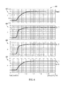
- FIG. 5 is a plot 500 which shows the current sharing and pre-bias startup operation for two power converters (e.g., two instances of power converter 100 ) connected together in parallel.
- FIG. 7 shows a schematic diagram for two power converters 100 - 1 and 100 - 2 which are coupled together in parallel. Specifically, the positive inputs +Vin 1 and +Vin 2 of the power converters 100 - 1 and 100 - 2 , respectively, are coupled together and coupled to a positive terminal of an input source Vin, and the negative inputs ⁇ Vin 1 and ⁇ Vin 2 of the power converters 100 - 1 and 100 - 2 , respectively, are coupled together and coupled to a negative terminal of the input source Vin.
- the outputs +V O1 and +V O2 of the power converters 100 - 1 and 100 - 2 , respectively, are coupled together and are coupled to a positive node of a load.
- the outputs ⁇ V O1 and ⁇ V O2 of the power converters 100 - 1 and 100 - 2 , respectively, are coupled together and are coupled to a negative node of the load.
- the “current sharing” or “common control” nodes IB 1 and IB 2 of the power converters 100 - 1 and 100 - 2 are coupled together.
- the output voltage V OUTPUT is pre-biased to a voltage of approximately 3 V by an external source. As shown, the output voltage V OUTPUT starts at 3 V and starts to rise at about 920 ⁇ s until the output voltage reaches regulation of 5 V at about 1.4 ms.
- a signal V ca1out , V ca2out represents the output signal of the op amp U 2 of the current error amplifier 116 for each of the two parallel-connected power converters 100 - 1 and 100 - 2 .
- a signal V ca1neg , V ca2neg represents the voltage at the inverting input of the op amp U 2 of the current error amplifier 116 for each of the two parallel-connected power converters 100 - 1 and 100 - 2 .
- Signal V ea1out and V ea2out represent an output voltage of the op amp U 1 of the voltage error amplifier 112 through the resistor R 8 for each of the two parallel-connected power converters 100 - 1 and 100 - 2 .
- a signal Vca 1 out, Vca 2 out represents the voltage at the output of the op amp U 2 of the current error amplifier 116 for each of the two parallel-connected power converters 100 - 1 and 100 - 2 .
- a signal IoShare represents the voltage of the current sharing or common control nodes IB 1 and IB 2 (see FIG. 7 ), which, as shown in FIG. 2B , is also the signal applied to the non-inverting input of the comparator U 3 of the current direction detector 118 and the signal applied to the non-inverting input of the op amp U 2 of the current error amplifier 116 through the resistor R 5 .
- the output signals V ca1out , V ca2out of the two current error amplifiers U 2 are also the feedback signals for the respective converters 100 - 1 and 100 - 2 .
- the waveforms shown in the plot 500 of FIG. 5 demonstrate that the error amplifiers U 1 and U 2 for the two power converters 100 - 1 and 100 - 2 are in control.
- FIG. 6 shows a diagram 600 which includes four plots 602 , 604 , 606 and 608 .
- the plot 602 shows the output voltage V OUTPUT of the two converters 100 - 1 and 100 - 2 connected in parallel.
- the plot 604 shows the average load current (I O - 1 ) through the output inductor L 6 ( FIG. 1 ) of the first power converter 100 - 1 .
- the plot 606 shows the average load current (I O - 2 ) through the output inductor L 6 of the second power converter 100 - 2 .
- the plot 608 shows the combined average load current (i.e., sum of I O - 1 and I O - 2 ) through the output inductors L 6 ( FIG.
- the output inductor L 6 for each of the power converters 100 - 1 and 100 - 2 carries an average of 5 A (plots 604 and 606 ) for a total of 10 A (plot 608 ) shared equally between the two converters.
- the implementations discussed herein provide several advantages.
- the implementations provide improved line and load transient responses, which allows such to be used in power converters with excellent stability and fast response.
- the implementations discussed herein provide current sharing capabilities with a single-control node by connecting multiple converters together via the common control node IB, as shown in FIGS. 2B and 7 .
- the “master” power converter in a group of two or more power converters is automatically determined by the power converter having the highest output voltage V O . If the master power converter is non-functional, then the next master power converter is determined automatically, and so on.
- the current sharing signal is provided for “free,” since all paralleled converters are connect together with a single connection (e.g., wire).
- the dynamic performance of the paralleled converters is the same as a single-converter since there's only one single-loop control at any given time.
- One or more implementations discussed herein also provide minimal part counts, which is beneficial for hybrid or other applications, and also provide enhanced radiation tolerance at low costs due to the use of discrete components. As discussed above, the implementations discussed herein prevent the synchronous MOSFETs M 4 and M 5 from oscillating during shutdown. Further, the state of the average current in the output inductor L 6 is used for multiple functions (e.g., detecting output current direction, setting current limit).
Abstract
A circuit for providing dynamic output current sharing using average current mode control for active-reset and self-driven synchronous rectification with pre-bias startup and redundancy capabilities for power converters. The circuit communicates a secondary side feedback signal to a primary side via a bidirectional magnetic communicator that also provides a secondary voltage supply. Pre-bias startup is achieved by detection of the output current direction and controlling the gate signals of synchronous rectifiers. The circuit permits dynamic current sharing via a single-control signal and automatic master converter selection and promotion.
Description
The present disclosure generally relates to power converters.
DC/DC converters are a type of power supply which converts an input DC voltage to a different output DC voltage. Such converters typically include a transformer that is electrically coupled via a switching circuit between a voltage source and a load. Converters known as forward converters include a main switch connected between the voltage source and the primary winding of the transformer to provide forward power transfer to the secondary winding of the transformer when the switch is on and conducting. A metal oxide semiconductor field effect transistor (MOSFET) device is typically used for the switch.
Power converter designs are often constrained by various requirements, such as efficiency, input voltage range, output voltage, power density, and footprint area. These constraints require certain performance tradeoffs. For instance, achieving higher efficiencies may require a more narrow input voltage range. To further improve efficiencies, active-reset schemes and synchronous rectifications are often employed. These synchronous rectification schemes can either be active-control or self-driven.
A limitation of forward converters is that it may be necessary to reset the transformer core to prevent saturation (i.e., discharge the magnetizing current of the transformer during the off period of the main switch). This limitation results from the unipolar character of the transformer core excitation. Techniques exist for resetting the transformer of a forward converter. One such technique is to include a resistor-capacitor-diode (RCD) network in parallel with the primary winding. The RCD network clamps the voltage on the switch to the minimal peak voltage consistent with a given source voltage and switch duty cycle, thereby eliminating the need for dead time while allowing for a wide range of duty cycles. This tends to reduce the voltage stress applied to the switch. Nevertheless, this transformer resetting technique reduces the efficiency of the converter due to the dissipation of the magnetizing energy accumulated in the transformer during the on period of the switch. Instead of being recycled, this magnetizing energy is partially converted into heat by the RCD network.
Another method of transformer resetting is to use a series connection of a capacitor and an auxiliary switch connected across the transformer winding either on the primary side or on the secondary side (referred to as an “active clamp” or “active reset”). When the main switch is turned off, the auxiliary switch is turned on, and vice versa. Thus, magnetizing energy in the transformer is transferred to the clamping capacitor, and the clamping capacitor resonates with the magnetizing inductance to maintain the necessary level of reset voltage. This active clamp reset provides non-dissipative reset of the transformer and minimal voltage stress on the main switch under steady state conditions as dead time is almost zero. For this reason, the active clamp method is compatible with self-driven synchronous rectification.
In switching power supply circuits employing synchronous rectifiers, the diodes are replaced by power transistors to obtain a lower on-state voltage drop. The synchronous rectifier generally uses n-channel MOSFETs rather than diodes to avoid the turn-on voltage drop of diodes which can be significant for low output voltage power supplies. The transistors are biased to conduct when a diode would have been conducting from anode to cathode, and conversely, are gated to block current when a diode would have been blocking from cathode to anode. Although MOSFETs usually serve this purpose, bipolar transistors and other active semiconductor switches may also be suitable.
In these synchronous rectifier circuits, the gate signals can be self-driven, i.e., the gate signal can be tied to the power circuit, or controlled-driven, i.e., the gate signal is derived from some point in the circuit and goes through some active processing circuit before being fed to the MOSFET gate driver. In a power converter, the synchronous rectifier which conducts during the non-conducting period of the main power switch (switches) may be referred to as a freewheeling or “catch” synchronous rectifier. The synchronous rectifier which conducts during the conducting period of the main power switch (switches) may be referred to as a forward synchronous rectifier.
In some applications, when a power converter is first turned on, a pre-existing voltage may exist at the output terminal. Such pre-existing voltage may be referred to as a pre-bias voltage, pre-charge voltage, reverse bias or back bias. This pre-bias voltage may result from an external voltage source (e.g., a load, another power converter), or may exist as a residual charge across one or more output capacitors of the power converter. As noted above, when synchronous rectifiers are used instead of diodes, such rectifiers (e.g., MOSFETs) allow current to flow through the switch in either direction. Thus, under some operating conditions, such as pre-bias startup, operation of the output switches may allow a reverse current to flow from the output terminal of the power converter to ground through an output inductor of the power converter. That is, in such instances the power converter acts as a current sink rather than a current source. Among other things, such undesirable operation may cause the output voltage to drop and may disturb or damage one or more components of the power converter.
An average current mode control (ACMC) controller for a power converter, the power converter including a power transformer having a primary winding electrically coupleable to an input voltage node and a secondary winding electrically coupleable to an output voltage node, a primary control circuit electrically coupled to the primary winding, a secondary control circuit electrically coupled to the secondary winding, the secondary control circuit including first and second synchronous rectifying elements including respective first and second control nodes, may be summarized as including a magnetic communicator circuit including a selectively controllable switch; and a coupling transformer including a first primary winding, a second primary winding, and a secondary winding, the secondary winding electrically coupled to a secondary side DC voltage supply circuit including a DC supply rectifier and a DC supply capacitor which provides a secondary side DC voltage supply on the DC supply capacitor of the secondary side DC voltage supply circuit, the first and second primary windings selectively coupled to a primary side DC voltage supply via the controllable switch whereby the secondary side DC voltage supply is developed on the DC supply capacitor of the secondary side DC voltage supply circuit by selectively controlling the controllable switch into conduction, the secondary winding electrically coupled to a secondary side feedback signal node, and the second primary winding electrically coupled to a sampling circuit including a sampling rectifier and a sampling capacitor whereby a secondary side feedback signal at the secondary side feedback signal node is transferred to the second primary winding by the selective controlling of the controllable switch into conduction, whereby a primary side feedback voltage is developed on the sampling capacitor of the sampling circuit by the selective controlling of the controllable switch into conduction, the primary side feedback voltage electrically coupleable to the primary control circuit of the power converter.
The ACMC controller may further include a voltage error amplifier circuit including an input node and an output node, the input node electrically coupled to the output voltage node of the power converter; and a current error amplifier circuit including an input node and an output node, the input node of the current error amplifier circuit electrically coupled to the output node of the voltage error amplifier circuit, and the output node of the current error amplifier electrically coupled to the secondary side feedback signal node. The voltage error amplifier circuit may include an operational amplifier which may include a supply input node electrically coupled to the secondary side DC voltage supply to receive power therefrom. The current error amplifier circuit may include an operational amplifier which may include a supply input node electrically coupled to the secondary side DC voltage supply to receive power therefrom.
The ACMC controller may further include a common control node which is representative of an output signal of the voltage error amplifier circuit, the common control node coupleable to a common control node of another power converter to provide current sharing operation between the power converter and the other power converter.
The ACMC controller may further include a current direction detector circuit operatively coupled to sense a direction of an output current of the power converter and, responsive to detecting output current flows into the power converter, the current direction detector circuit causes the first and second control nodes of the respective first and second synchronous rectifying elements to control the first and second synchronous rectifying elements to be in an non-conduction state. The current direction detector circuit may include a comparator which may include a supply input node electrically coupled to the secondary side DC voltage supply to receive power therefrom. The current direction detector circuit may include a control switch electrically coupled to each of the first and second control nodes of the respective first and second synchronous rectifying elements, the control switch including a control switch control node electrically coupled to the output voltage node of the power converter. The current direction detector may include a control switch electrically coupled to each of the first and second control nodes of the respective first and second synchronous rectifying elements via respective first and second diodes, the control switch including a control switch control node electrically coupled to the output voltage node of the power converter via a resistor.
An active-clamp forward converter may be summarized as including a transformer having a primary winding and a secondary winding, the secondary winding electrically coupleable to an output voltage node; a primary circuit electrically coupled to the primary winding, the primary winding electrically coupleable to an input voltage node; a secondary circuit electrically coupled to the secondary winding, the secondary circuit including first and second synchronous rectifying elements including respective first and second control nodes; and an average current mode control (ACMC) converter, including a magnetic communicator circuit including a selectively controllable switch; and a coupling transformer including a first primary winding, a second primary winding, and a secondary winding, the secondary winding electrically coupled to a secondary side DC voltage supply circuit including a DC supply rectifier and a DC supply capacitor which provides a secondary side DC voltage supply on the DC supply capacitor of the secondary side DC voltage supply circuit, the first and second primary windings selectively coupled to a primary side DC voltage supply via the controllable switch whereby the secondary side DC voltage supply is developed on the DC supply capacitor of the secondary side DC voltage supply circuit by selectively controlling the controllable switch into conduction, the secondary winding electrically coupled to a secondary side feedback signal node, and the second primary winding electrically coupled to a sampling circuit including a sampling rectifier and a sampling capacitor whereby a secondary side feedback signal at the secondary side feedback signal node is transferred to the second primary winding by the selective controlling of the controllable switch into conduction, whereby a primary side feedback voltage is developed on the sampling capacitor of the sampling circuit by the selective controlling of the controllable switch into conduction, the primary side feedback voltage electrically coupleable to the primary control circuit of the forward converter.
The active-clamp forward converter may further include a voltage error amplifier circuit including an input node and an output node, the input node electrically coupled to the output voltage node of the forward converter; and a current error amplifier circuit including an input node and an output node, the input node of the current error amplifier electrically coupled to the output node of the voltage error amplifier circuit, and the output node of the current error amplifier electrically coupled to the secondary side feedback signal node. The voltage error amplifier circuit may include an operational amplifier which may include a supply input node electrically coupled to the secondary side DC voltage supply to receive power therefrom. The current error amplifier circuit may include an operational amplifier which may include a supply input node electrically coupled to the secondary side DC voltage supply to receive power therefrom.
The active-clamp forward converter may further include a common control node which is representative of an output signal of the voltage error amplifier circuit, the common control node coupleable to a common control node of another forward converter to provide current sharing operation between the forward converter and the other forward converter.
The active-clamp forward converter may further include a current direction detector circuit operatively coupled to sense a direction of an output current of the forward converter and, responsive to detecting output current flows into the forward converter, the current direction detector circuit causes the first and second control nodes of the respective first and second synchronous rectifying elements to control the first and second synchronous rectifying elements to be in an non-conduction state. The current direction detector circuit may include a comparator which may include a supply input node electrically coupled to the secondary side DC voltage supply to receive power therefrom. The current direction detector may include a control switch electrically coupled to each of the first and second control nodes of the respective first and second synchronous rectifying elements, the control switch including a control switch control node electrically coupled to the output voltage node of the forward converter. The current direction detector may include a control switch electrically coupled to each of the first and second control nodes of the respective first and second synchronous rectifying elements via respective first and second diodes, the control switch including a control switch control node electrically coupled to the output voltage node of the forward converter via a resistor.
An average current mode control (ACMC) controller for a power converter, the power converter including a power transformer having a primary winding electrically coupleable to an input voltage node and a secondary winding electrically coupleable to an output voltage node, a primary control circuit electrically coupled to the primary winding, a secondary control circuit electrically coupled to the secondary winding, the secondary control circuit including first and second synchronous rectifying elements including respective first and second control nodes, may be summarized as including a voltage error amplifier circuit including an input node and an output node, the input node electrically coupled to the output voltage node of the power converter; a current error amplifier circuit including an input node and an output node, the input node of the current error amplifier electrically coupled to the output node of the voltage error amplifier circuit, and the output node of the current error amplifier electrically coupled to a secondary side feedback signal node; and a current direction detector circuit operatively coupled to sense a direction of an output current of the power converter and, responsive to detecting output current flows into the power converter, the current direction detector circuit causes the first and second control nodes of the respective first and second synchronous rectifying elements to control the first and second synchronous rectifying elements to be in an non-conduction state. The current direction detector circuit may include a comparator which may include a supply input node electrically coupled to a secondary side DC voltage supply circuit to receive power therefrom. The current direction detector may include a control switch electrically coupled to each of the first and second control nodes of the respective first and second synchronous rectifying elements, the control switch including a control switch control node electrically coupled to the output voltage node of the power converter.
The ACMC controller may further include a magnetic communicator circuit including a selectively controllable switch; and a coupling transformer including a first primary winding, a second primary winding, and a secondary winding, the secondary winding electrically coupled to a secondary side DC voltage supply circuit including a DC supply rectifier and a DC supply capacitor which provides a secondary side DC voltage supply on the DC supply capacitor of the secondary side DC voltage supply circuit, the first and second primary windings selectively coupled to a primary side DC voltage supply via the controllable switch whereby the secondary side DC voltage supply is developed on the DC supply capacitor of the secondary side DC voltage supply circuit by selectively controlling the controllable switch into conduction, the secondary winding electrically coupled to the secondary side feedback signal node, and the second primary winding electrically coupled to a sampling circuit including a sampling rectifier and a sampling capacitor whereby a secondary side feedback signal at the secondary side feedback signal node is transferred to the second primary winding by the selective controlling of the controllable switch into conduction, whereby a primary side feedback voltage is developed on the sampling capacitor of the sampling circuit by the selective controlling of the controllable switch into conduction, the primary side feedback voltage electrically coupleable to the primary control circuit of the power converter. The current direction detector may include a control switch electrically coupled to each of the first and second control nodes of the respective first and second synchronous rectifying elements via respective first and second diodes, the control switch including a control switch control node electrically coupled to the output voltage node of the power converter via a resistor.
The ACMC controller may further include a common control node which is representative of an output signal of the voltage error amplifier circuit, the common control node coupleable to a common control node of another power converter to provide current sharing operation between the power converter and the other power converter.
In the drawings, identical reference numbers identify similar elements or acts. The sizes and relative positions of elements in the drawings are not necessarily drawn to scale. For example, the shapes of various elements and angles are not necessarily drawn to scale, and some of these elements may be arbitrarily enlarged and positioned to improve drawing legibility. Further, the particular shapes of the elements as drawn, are not necessarily intended to convey any information regarding the actual shape of the particular elements, and may have been solely selected for ease of recognition in the drawings.
In the following description, certain specific details are set forth in order to provide a thorough understanding of various disclosed implementations. However, one skilled in the relevant art will recognize that implementations may be practiced without one or more of these specific details, or with other methods, components, materials, etc. In other instances, well-known structures associated with computer systems, server computers, and/or communications networks have not been shown or described in detail to avoid unnecessarily obscuring descriptions of the implementations.
Unless the context requires otherwise, throughout the specification and claims that follow, the word “comprising” is synonymous with “including,” and is inclusive or open-ended (i.e., does not exclude additional, unrecited elements or method acts).
Reference throughout this specification to “one implementation” or “an implementation” means that a particular feature, structure or characteristic described in connection with the implementation is included in at least one implementation. Thus, the appearances of the phrases “in one implementation” or “in an implementation” in various places throughout this specification are not necessarily all referring to the same implementation. Furthermore, the particular features, structures, or characteristics may be combined in any suitable manner in one or more implementations.
As used in this specification and the appended claims, the singular forms “a,” “an,” and “the” include plural referents unless the context clearly dictates otherwise. It should also be noted that the term “or” is generally employed in its sense including “and/or” unless the context clearly dictates otherwise.
The headings and Abstract of the Disclosure provided herein are for convenience only and do not interpret the scope or meaning of the implementations.
One or more implementations of the present disclosure provide discrete implementations of power converter controllers which utilize average current mode control (ACMC) with pre-bias startup and current sharing capabilities for power converters which utilize an active reset scheme and self-driven synchronous rectification (SDSR). One or more implementations discussed herein solve or improve inherent issues with SDSR including, but not limited to, pre-bias startup, current sharing and redundancy capabilities. Inherent to SDSR is an oscillation that occurs on the synchronous MOSFETs during shutdown, which is not a desirable behavior. Without a control method as discussed herein, an externally applied output voltage may turn-on the synchronous rectifiers causing the power converter to sink current instead of sourcing current. One or more implementations discussed herein solve one or more issues with SDSR power converters utilizing a relatively few number of discrete components. Such implementations of the present disclosure may be ideal for hybrid applications, especially for applications where radiation tolerance and minimal part counts are important for high power density.
More particularly, the systems and methods discussed herein may allow one or more power converters to start up into regulation with an external voltage source already applied to its output terminal. As noted above, this feature may be referred to as pre-bias startup. Further, multiple power converters may be connected in parallel to deliver more power to a load than is possible with a single power converter. As discussed further below, this current sharing feature may be performed by connecting the output terminals of multiple power converters together and connecting respective “current sharing” or “common control” nodes of the power converters together. Such feature may also provide redundancy in the event of failure of one or more of the multiple power converters and/or failure of one or more power sources to which the one or more power converters are connected.
A secondary winding L5 of the transformer T1 is connected to an output node VO through a synchronous rectifier including MOSFET rectifying devices M4 and M5. Each rectifying device M4 and M5 includes a body diode. With the power switch M2 conducting, the input voltage VIN is applied across the primary winding L4. The secondary winding L5 is oriented in polarity to respond to the primary voltage with a current flow through an output inductor L6, through a load R6 connected to the output node VO, and back through the MOSFET rectifier device M4 to the secondary winding L5. Continuity of the current flow in the output inductor L6 when the power switch M2 is non-conducting is maintained by the current path provided by the conduction of the MOSFET rectifier device M5. An output filter capacitor C7 shunts the output of the power converter 100.
Conductivity of the two rectifier devices M4 and M5 is controlled by SDSR logic 104 which may optionally receive signals by a primary active-reset pulse-width modulated (PWM) controller 106. The active-reset controller 106 may include, for example, one or more oscillators, comparators, and/or flip-flops. The output of the active reset controller 106 may provide a PWM drive signal to the main switch M2 and the auxiliary switch M3.
The power converter 100 may also include an ACMC controller 110 which operates to control the power converter utilizing average current mode control. Generally, current mode control is a two-loop system which includes an outer voltage control loop and an inner current control loop.
Compared to ACMC which is implemented in the present disclosure, peak current control mode has some deficiencies. In particular, peak current control mode operates by directly comparing the output inductor current waveform to a current program level, set by the outer voltage loop, at two inputs of a PWM comparator. The inner current control loop has a low gain and thus cannot correct for some deficiencies, including poor noise immunity, requirement for slope compensation, and peak-to-average current error.
To remedy some performance issues with peak current mode control, ACMC is used in the implementations of the present disclosure. ACMC overcomes some or all of these deficiencies by providing a high gain integrating current error amplifier into the inner current control loop. Generally, a current error signal is amplified and compared to a relatively large oscillator ramp (e.g., sawtooth) at the inputs of a PWM comparator provided by the active reset controller 106.
As shown in FIG. 1 , the ACMC controller 110 includes five primary functional blocks. Such functional blocks include a voltage error amplifier 112, a current sensor 114, a current error amplifier 116, a current direction detector 118, and a magnetic communicator 120. Each of these functional blocks is discussed below.
The voltage error amplifier 112 receives the output voltage VO of the power converter 100 as input and controls an outer voltage control loop by comparing the output voltage VO to a fixed reference voltage. This voltage error signal is fed to the current error amplifier 116.
The current sensor 114 is operative to sense the output current of the power converter 100, and to generate an output signal which is representative of (e.g., proportional to) the output current of the power converter 100. The current sensor 114 may include one or more sensing resistors, current sense transformers, and/or other current sensing circuitry, for example.
The current error amplifier 116 may be an integrating current error amplifier which controls an inner current control loop of the ACMC controller 110. The current error amplifier 116 may compare a signal received from the current sensor 114 to a current program signal supplied by the voltage error amplifier 112.
The current direction detector 118 receives the output signal from the voltage error amplifier 112 which is used to determine the direction of the output current of the power converter 100. The current direction detector 118 primarily functions to detect the direction of the output current LLOAD across the load, which in the schematic diagrams of FIGS. 1 and 2A-2B is represented by a load resistor R6. If the current direction detector 118 determines that the power converter 100 is sinking current, for example, due to an externally applied output voltage, represented in the schematic diagrams as a voltage source V1 coupled to the load resistor R6 via a diode D12, then the current direction detector controls the synchronous MOSFETs M4 and M5 via gate nodes G2 and G1, respectively, to remain off to prevent the power converter from sinking current. In at least some implementations, the current direction detector 118 detects a negative current when (1) the power converter 100 is inhibited to prevent the converter output from shorting the load, or (2) during shutdown when power can be passed from the secondary-side to the primary-side causing a negative current for the voltage error amplifier 112 such that the voltage at the inverting pin is greater than the voltage of the non-inverting pin, which causes the output of the voltage error amplifier to go to zero, which in turn causes the output of the current direction detector to go to zero.
The voltage source V1 is representative of a source of voltage, such as another power converter coupled in parallel to the power converter 100, etc. As discussed further below, this feature allows for pre-bias startup and output current sharing. In at least one implementation, during a power loss the current direction detector 118 utilizes the output voltage VO to turn off the MOSFETs M4 and M5, which advantageously functions to preserve the output voltage VO by preventing the power converter 100 from sinking current which would otherwise discharge the output capacitor C7 and may cause undesirable behavior or damage to the power converter 100.
The magnetic communicator 120 provides multiple bidirectional functions. First, the magnetic communicator 120 provides isolated transformer-coupled magnetic feedback to the active reset controller 106. Generally, the magnetic communicator 120 employs a transformer, a modulator, and a demodulator to allow optimization of a feedback path which provides an isolation barrier 122 between an input side and an output side of the power converter 100. Second, the magnetic communicator 120 receives a primary side voltage supply VCCP and provides a secondary side voltage supply VCCS which may be used by one or more components of the voltage error amplifier 112, the current sensor 114, the current error amplifier 116 or the current direction detector 118. Third, the magnetic communicator 120 provides an input to the current direction detector 118 supply input (i.e., VCCS). When the secondary supply voltage VCCS disappears due to a power loss (e.g., shutdown), the current direction detector 118 keeps the gate signals G1 and G2 low, which turns off the synchronous MOSFETs M4 and M5 to prevent them from conducting current.
The current error amplifier 116 includes the op amp U2, resistors R4, R9, R10, and a capacitor C2. The op amp U2 may be powered by the secondary side voltage supply VCCS provided by the magnetic communicator 120. An output node FB1 of the current error amplifier 116 is provided to the magnetic communicator 120, as discussed further below. To achieve average current control, the inner current loop is controlled by the op amp U2. The output of the op amp U1 of the voltage error amplifier 112 is compared to a current sense signal from the current sensor 114 which comprises a current source I1, a resistor R12 and a Zener diode D9. The current source I1 is not literal. Rather, the current source I1 represents the transducing of the average current of the output inductor L6 to a representative voltage conversion using R12.
Referring to FIG. 2A , the magnetic communicator 120 may utilize “flyback sampling” to provide continuous monitoring of the average current error signal provided by the output node FB1 of the op amp U2 of the current error amplifier 116. The magnetic communicator 120 includes a coupling transformer T2 which has primary side windings L1 and L2 and a secondary side winding L3. The winding L1 is between nodes T2A and T2B, the winding L2 is between nodes T2C and T2D, and the winding L3 is between nodes T2E and T2F. The turns ratio for the windings L1, L2, and L3 may be any turns ratio suitable for a particular application, for example, 1:1:1, 1:1:2, etc. A fixed frequency pulse signal may be provided at a sampling switch control node FBP which is coupled to a gate node of a switch M1. The switch M1 may be any type of suitable switch (e.g., MOSFET).
When the switch M1 is turned on, the winding L1 of the transformer T2 is coupled to a primary side voltage supply VCCP. This causes a magnetizing energy to build up in the transformer T2. At this time, the voltage across nodes T2C-D of winding L2 is negative at the anode of a diode D10 so the diode D10 is not conducting. A diode D6 prevents the voltage VCCP from appearing at the secondary side of T2 and interfering with the current error amplifier 116. When the switch M1 is turned on, the VCCP voltage is transferred from T2A-B to T2E-F, which is then peak-charged into the capacitor C5 by diodes D5 and D3 to supply the secondary side voltage supply VCCS for the op amp U2 of the current error amplifier 116 and the op amp U1 of the voltage error amplifier 112.
When the switch M1 is turned off, the magnetizing energy stored in the transformer T2 returns in the form of a flyback voltage. That voltage is clamped by error signal FB2 via diodes D6 and D4. The current error amplifier 116 has a low impedance provided by an emitter follower buffer Q3. During the flyback time, the error signal FB2 is fed back to the primary side of the transformer T2 by the voltage reflected across nodes T2C and T2D which is then peak-charged into the capacitor C6 through the diode D10 to form the primary-side feedback signal VFB1 for the active reset controller 106. The conditioned load voltage VFB2 is equal to the voltage at the node FB2 plus the forward diode drop of the diode D6. A resistor R20 may be provided to control the discharge rate of the capacitor C6.
As discussed above, the current direction detector 118 functions to determine whether the output current ILOAD flows into or out of the power converter 100. The current direction detector 118 in this example includes a comparator U3, the Zener diode D9, resistors R13, R16, R17, and R18, diodes D7 and D8, and switches Q4 and Q5. As discussed above, the current source I1 provides a signal which is representative of the average load current LOAD. The current source I1 may comprise a current transformer on the primary power transformer T1, a current sensing resistor, etc.
In operation, the current direction detector 118 turns off the synchronous MOSFETs M4 and M5 when it is determined that current is flowing into the power converter 100 rather than out of the power converter. This may be achieved by directing the synchronous rectification MOSFETs M4 and M5 to remain off by turning the switch Q4 off and turning the switch Q5 on. In particular, when a “negative current” (i.e., into the power converter 100) is detected by the comparator U3, the gate signals G1 and G2 are pulled to ground through conduction of the diodes D7 and D8 to prevent the synchronous MOSFETs M4 and M5 from conducting current. This occurs when the switch Q5 is on, the switch Q4 is off, and the output of the comparator U3 is low (i.e., 0 V). For the output of the comparator U3 to be low, the positive input of the comparator U3 must be less than the negative input of the comparator U3. The negative input of the comparator U3 is a fixed positive voltage formed by the Zener diode D9.
As shown in FIG. 2B , the base of the switch Q5 is coupled to the output node VO through the resistor R18. When the output of the comparator U3 is low, the switch Q4 is turned off which causes the switch Q5 to be turned on due to the voltage provided by the output voltage VO. When the switch Q5 is turned on, current flows through the diodes D7 and D8 which keeps the gate signals G1 and G2 low, thereby keeping the synchronous MOSFETs M4 and M5 turned off. Thus, during a power loss, the current direction detector 118 utilizes the output voltage VO to turn off the MOSFETs M4 and M5, which advantageously functions to preserve the output voltage VO by preventing the power converter 100 from sinking current which would otherwise rapidly discharge the output capacitor C7. This feature is accomplished without requiring any input voltage VIN.
Thus, the synchronous MOSFETs M4 and M5 are kept turned off when the output voltage VO is greater than the base-emitter voltage (Vbe) of the switch Q5 due to an external source (e.g., source V1) and the output of the comparator U3 is low, which indicates a negative or reverse current into the power converter 100. The synchronous MOSFETs are also kept turned off when the secondary side supply voltage VCCS is low (e.g., due to loss of power).
As briefly discussed above, in one or more implementations the magnetic communicator 120 provides at least three functions. First, the magnetic communicator 120 provides the secondary side voltage supply VCCS when the switch M1 is turned on. Second, the magnetic communicator 120 provides isolated magnetic feedback from the secondary side to the primary side during the portion of the cycle when the switch M1 is turned off. Third, the magnetic communicator 120 provides the secondary side voltage supply VCCS to the comparator U3 of the current direction detector 118. When the secondary side supply voltage VCCS is lost (e.g., shutdown, inhibit), the output of the comparator U3 goes low, which turns the switch Q4 off and turns the switch Q5 on. As discussed above, this feature keeps the gate nodes G1 and G2 of the synchronous MOSFETs M5 and M4, respectively, low, which keeps the MOSFETs M4 and M5 turned off to prevent current from flowing into the power converter 100.
As noted above, inherent to SDSR is an oscillation on the synchronous MOSFETs (e.g., MOSFETs M4 and M5) that occurs during shutdown. The implementations discussed herein prevent this behavior by removing the secondary voltage VCCS from the comparator U3 of the current direction detector 118 when the switch M1 turns off. This event causes the switch Q4 to turn off and the switch Q5 to turn on, thereby keeping the gate nodes G1 and G2 clamped to ground plus a diode forward voltage drop of diodes D7 and D8, respectively. As a result, the synchronous MOSFETs M4 and M5 no longer oscillate when the power converter 100 is shut down, and the output capacitor(s) C7 is no longer discharged.
As shown in FIG. 3 , in this example the output voltage VOUTPUT is pre-biased at a point 302 to about 3 V by the external voltage source V1. In practice, the pre-biased voltage may be provided by the load or by one or more additional power converters. As shown, the power converter 100 starts up at a point 304, where the circuitry is activated, and continues until point 306 where the output voltage VO is regulated at 5 V.
Referring back to FIG. 5 , in this example, the output voltage VOUTPUT is pre-biased to a voltage of approximately 3 V by an external source. As shown, the output voltage VOUTPUT starts at 3 V and starts to rise at about 920 μs until the output voltage reaches regulation of 5 V at about 1.4 ms.
In the plot 500 of FIG. 5 , a signal Vca1out, Vca2out represents the output signal of the op amp U2 of the current error amplifier 116 for each of the two parallel-connected power converters 100-1 and 100-2. A signal Vca1neg, Vca2neg represents the voltage at the inverting input of the op amp U2 of the current error amplifier 116 for each of the two parallel-connected power converters 100-1 and 100-2. Signal Vea1out and Vea2out represent an output voltage of the op amp U1 of the voltage error amplifier 112 through the resistor R8 for each of the two parallel-connected power converters 100-1 and 100-2. A signal Vca1out, Vca2out represents the voltage at the output of the op amp U2 of the current error amplifier 116 for each of the two parallel-connected power converters 100-1 and 100-2. A signal IoShare represents the voltage of the current sharing or common control nodes IB1 and IB2 (see FIG. 7 ), which, as shown in FIG. 2B , is also the signal applied to the non-inverting input of the comparator U3 of the current direction detector 118 and the signal applied to the non-inverting input of the op amp U2 of the current error amplifier 116 through the resistor R5.
As discussed above, the output signals Vca1out, Vca2out of the two current error amplifiers U2 are also the feedback signals for the respective converters 100-1 and 100-2. The waveforms shown in the plot 500 of FIG. 5 demonstrate that the error amplifiers U1 and U2 for the two power converters 100-1 and 100-2 are in control.
As discussed above, the implementations discussed herein provide several advantages. The implementations provide improved line and load transient responses, which allows such to be used in power converters with excellent stability and fast response. Further, the implementations discussed herein provide current sharing capabilities with a single-control node by connecting multiple converters together via the common control node IB, as shown in FIGS. 2B and 7 . When in current sharing operation, the “master” power converter in a group of two or more power converters is automatically determined by the power converter having the highest output voltage VO. If the master power converter is non-functional, then the next master power converter is determined automatically, and so on. Further, the current sharing signal is provided for “free,” since all paralleled converters are connect together with a single connection (e.g., wire). The dynamic performance of the paralleled converters is the same as a single-converter since there's only one single-loop control at any given time.
One or more implementations discussed herein also provide minimal part counts, which is beneficial for hybrid or other applications, and also provide enhanced radiation tolerance at low costs due to the use of discrete components. As discussed above, the implementations discussed herein prevent the synchronous MOSFETs M4 and M5 from oscillating during shutdown. Further, the state of the average current in the output inductor L6 is used for multiple functions (e.g., detecting output current direction, setting current limit).
The foregoing detailed description has set forth various implementations of the devices and/or processes via the use of block diagrams, schematics, and examples. Insofar as such block diagrams, schematics, and examples contain one or more functions and/or operations, it will be understood by those skilled in the art that each function and/or operation within such block diagrams, flowcharts, or examples can be implemented, individually and/or collectively, by a wide range of hardware, software, firmware, or virtually any combination thereof. In one implementation, the present subject matter may be implemented via Application Specific Integrated Circuits (ASICs). Those of skill in the art will recognize that many of the methods or algorithms set out herein may employ additional acts, may omit some acts, and/or may execute acts in a different order than specified.
The various implementations described above can be combined to provide further implementations. Aspects of the implementations can be modified, if necessary, to employ systems, circuits and concepts of the various patents, applications and publications to provide yet further implementations.
These and other changes can be made to the implementations in light of the above-detailed description. In general, in the following claims, the terms used should not be construed to limit the claims to the specific implementations disclosed in the specification and the claims, but should be construed to include all possible implementations along with the full scope of equivalents to which such claims are entitled. Accordingly, the claims are not limited by the disclosure.
Claims (19)
1. An average current mode control (ACMC) controller for a power converter, the power converter comprising a power transformer having a primary winding electrically coupleable to an input voltage node and a secondary winding electrically coupleable to an output voltage node, a primary control circuit electrically coupled to the primary winding, a secondary control circuit electrically coupled to the secondary winding, the secondary control circuit comprising first and second synchronous rectifying elements comprising respective first and second control nodes, the average current mode control (ACMC) controller comprising:
a magnetic communicator circuit comprising:
a selectively controllable switch; and
a coupling transformer comprising a first primary winding, a second primary winding, and a secondary winding, the secondary winding electrically coupled to a secondary side DC voltage supply circuit comprising a DC supply rectifier and a DC supply capacitor which provides a secondary side DC voltage supply on the DC supply capacitor of the secondary side DC voltage supply circuit, the first and second primary windings selectively coupled to a primary side DC voltage supply via the controllable switch whereby the secondary side DC voltage supply is developed on the DC supply capacitor of the secondary side DC voltage supply circuit by selectively controlling the controllable switch into conduction, the secondary winding electrically coupled to a secondary side feedback signal node, and the second primary winding electrically coupled to a sampling circuit comprising a sampling rectifier and a sampling capacitor whereby a secondary side feedback signal at the secondary side feedback signal node is transferred to the second primary winding by the selective controlling of the controllable switch into conduction, whereby a primary side feedback voltage is developed on the sampling capacitor of the sampling circuit by the selective controlling of the controllable switch into conduction, the primary side feedback voltage electrically coupleable to the primary control circuit of the power converter.
2. The average current mode control (ACMC) controller of claim 1 , further comprising:
a voltage error amplifier circuit comprising an input node and an output node, the input node electrically coupled to the output voltage node of the power converter; and
a current error amplifier circuit comprising an input node and an output node, the input node of the current error amplifier circuit electrically coupled to the output node of the voltage error amplifier circuit, and the output node of the current error amplifier electrically coupled to the secondary side feedback signal node.
3. The average current mode control (ACMC) controller of claim 2 wherein the voltage error amplifier circuit comprises an operational amplifier which includes a supply input node electrically coupled to the secondary side DC voltage supply to receive power therefrom.
4. The average current mode control (ACMC) controller of claim 2 wherein the current error amplifier circuit comprises an operational amplifier which includes a supply input node electrically coupled to the secondary side DC voltage supply to receive power therefrom.
5. The average current mode control (ACMC) controller of claim 2 , further comprising:
a common control node which is representative of an output signal of the voltage error amplifier circuit, the common control node coupleable to a common control node of another power converter to provide current sharing operation between the power converter and the other power converter.
6. The average current mode control (ACMC) controller of claim 1 , further comprising:
a current direction detector circuit operatively coupled to sense a direction of an output current of the power converter and, responsive to detecting output current flows into the power converter, the current direction detector circuit causes the first and second control nodes of the respective first and second synchronous rectifying elements to control the first and second synchronous rectifying elements to be in an non-conduction state.
7. The average current mode control (ACMC) controller of claim 6 wherein the current direction detector circuit comprises a comparator which includes a supply input node electrically coupled to the secondary side DC voltage supply to receive power therefrom.
8. The average current mode control (ACMC) controller of claim 6 wherein the current direction detector circuit comprises a control switch electrically coupled to each of the first and second control nodes of the respective first and second synchronous rectifying elements, the control switch comprising a control switch control node electrically coupled to the output voltage node of the power converter.
9. The average current mode control (ACMC) controller of claim 6 wherein the current direction detector comprises a control switch electrically coupled to each of the first and second control nodes of the respective first and second synchronous rectifying elements via respective first and second diodes, the control switch comprising a control switch control node electrically coupled to the output voltage node of the power converter via a resistor.
10. An active-clamp forward converter, comprising:
a transformer having a primary winding and a secondary winding, the secondary winding electrically coupleable to an output voltage node;
a primary control circuit electrically coupled to the primary winding, the primary winding electrically coupleable to an input voltage node;
a secondary control circuit electrically coupled to the secondary winding, the secondary control circuit comprising first and second synchronous rectifying elements comprising respective first and second control nodes; and
an average current mode control (ACMC) converter, comprising:
a magnetic communicator circuit comprising:
a selectively controllable switch; and
a coupling transformer comprising a first primary winding, a second primary winding, and a secondary winding, the secondary winding electrically coupled to a secondary side DC voltage supply circuit comprising a DC supply rectifier and a DC supply capacitor which provides a secondary side DC voltage supply on the DC supply capacitor of the secondary side DC voltage supply circuit, the first and second primary windings selectively coupled to a primary side DC voltage supply via the controllable switch whereby the secondary side DC voltage supply is developed on the DC supply capacitor of the secondary side DC voltage supply circuit by selectively controlling the controllable switch into conduction, the secondary winding electrically coupled to a secondary side feedback signal node, and the second primary winding electrically coupled to a sampling circuit comprising a sampling rectifier and a sampling capacitor whereby a secondary side feedback signal at the secondary side feedback signal node is transferred to the second primary winding by the selective controlling of the controllable switch into conduction, whereby a primary side feedback voltage is developed on the sampling capacitor of the sampling circuit by the selective controlling of the controllable switch into conduction, the primary side feedback voltage electrically coupleable to the primary control circuit of the active-clamp forward converter.
11. The active-clamp forward converter of claim 10 , further comprising:
a voltage error amplifier circuit comprising an input node and an output node, the input node electrically coupled to the output voltage node of the active-clamp forward converter; and
a current error amplifier circuit comprising an input node and an output node, the input node of the current error amplifier electrically coupled to the output node of the voltage error amplifier circuit, and the output node of the current error amplifier electrically coupled to the secondary side feedback signal node.
12. The active-clamp forward converter of claim 11 wherein the voltage error amplifier circuit comprises an operational amplifier which includes a supply input node electrically coupled to the secondary side DC voltage supply to receive power therefrom.
13. The active-clamp forward converter of claim 11 wherein the current error amplifier circuit comprises an operational amplifier which includes a supply input node electrically coupled to the secondary side DC voltage supply to receive power therefrom.
14. The active-clamp forward converter of claim 11 , further comprising:
a common control node which is representative of an output signal of the voltage error amplifier circuit, the common control node coupleable to a common control node of another active-clamp forward converter to provide current sharing operation between the active-clamp forward converter and the other active-clamp forward converter.
15. The active-clamp forward converter of claim 10 , further comprising:
a current direction detector circuit operatively coupled to sense a direction of an output current of the active-clamp forward converter and, responsive to detecting output current flows into the active-clamp forward converter, the current direction detector circuit causes the first and second control nodes of the respective first and second synchronous rectifying elements to control the first and second synchronous rectifying elements to be in an non-conduction state.
16. The active-clamp forward converter of claim 15 wherein the current direction detector circuit comprises a comparator which includes a supply input node electrically coupled to the secondary side DC voltage supply to receive power therefrom.
17. The active-clamp forward converter of claim 15 wherein the current direction detector comprises a control switch electrically coupled to each of the first and second control nodes of the respective first and second synchronous rectifying elements, the control switch comprising a control switch control node electrically coupled to the output voltage node of the active-clamp forward converter.
18. The active-clamp forward converter of claim 15 wherein the current direction detector comprises a control switch electrically coupled to each of the first and second control nodes of the respective first and second synchronous rectifying elements via respective first and second diodes, the control switch comprising a control switch control node electrically coupled to the output voltage node of the active-clamp forward converter via a resistor.
19. An average current mode control (ACMC) controller for a power converter, the power converter comprising a power transformer having a primary winding electrically coupleable to an input voltage node and a secondary winding electrically coupleable to an output voltage node, a primary control circuit electrically coupled to the primary winding, a secondary control circuit electrically coupled to the secondary winding, the secondary control circuit comprising first and second synchronous rectifying elements comprising respective first and second control nodes, the average current mode control (ACMC) controller comprising:
a voltage error amplifier circuit comprising an input node and an output node, the input node electrically coupled to the output voltage node of the power converter;
a current error amplifier circuit comprising an input node and an output node, the input node of the current error amplifier electrically coupled to the output node of the voltage error amplifier circuit, and the output node of the current error amplifier electrically coupled to a secondary side feedback signal node;
a current direction detector circuit operatively coupled to sense a direction of an output current of the power converter and, responsive to detecting output current flows into the power converter, the current direction detector circuit causes the first and second control nodes of the respective first and second synchronous rectifying elements to control the first and second synchronous rectifying elements to be in an non-conduction state; and
a magnetic communicator circuit comprising:
a selectively controllable switch; and
a coupling transformer comprising a first primary winding, a second primary winding, and a secondary winding, the secondary winding electrically coupled to a secondary side DC voltage supply circuit comprising a DC supply rectifier and a DC supply capacitor which provides a secondary side DC voltage supply on the DC supply capacitor of the secondary side DC voltage supply circuit, the first and second primary windings selectively coupled to a primary side DC voltage supply via the controllable switch whereby the secondary side DC voltage supply is developed on the DC supply capacitor of the secondary side DC voltage supply circuit by selectively controlling the controllable switch into conduction, the secondary winding electrically coupled to the secondary side feedback signal node, and the second primary winding electrically coupled to a sampling circuit comprising a sampling rectifier and a sampling capacitor whereby a secondary side feedback signal at the secondary side feedback signal node is transferred to the second primary winding by the selective controlling of the controllable switch into conduction, whereby a primary side feedback voltage is developed on the sampling capacitor of the sampling circuit by the selective controlling of the controllable switch into conduction, the primary side feedback voltage electrically coupleable to the primary control circuit of the power converter.
Priority Applications (5)
| Application Number | Priority Date | Filing Date | Title |
|---|---|---|---|
| US15/178,968 US9780635B1 (en) | 2016-06-10 | 2016-06-10 | Dynamic sharing average current mode control for active-reset and self-driven synchronous rectification for power converters |
| PCT/US2017/035932 WO2017214027A1 (en) | 2016-06-10 | 2017-06-05 | Dynamic sharing average current mode control for active-reset and self-driven synchronous rectification for power converters |
| CN201780035100.XA CN109314468B (en) | 2016-06-10 | 2017-06-05 | Dynamic shared average current mode control for active reset and self-driven synchronous rectification of power converters |
| TW106118464A TWI740956B (en) | 2016-06-10 | 2017-06-05 | Average current mode control (acmc) controller for a power converter and active-clamp forward converter |
| US15/652,849 US9866100B2 (en) | 2016-06-10 | 2017-07-18 | Dynamic sharing average current mode control for active-reset and self-driven synchronous rectification for power converters |
Applications Claiming Priority (1)
| Application Number | Priority Date | Filing Date | Title |
|---|---|---|---|
| US15/178,968 US9780635B1 (en) | 2016-06-10 | 2016-06-10 | Dynamic sharing average current mode control for active-reset and self-driven synchronous rectification for power converters |
Related Child Applications (1)
| Application Number | Title | Priority Date | Filing Date |
|---|---|---|---|
| US15/652,849 Continuation US9866100B2 (en) | 2016-06-10 | 2017-07-18 | Dynamic sharing average current mode control for active-reset and self-driven synchronous rectification for power converters |
Publications (1)
| Publication Number | Publication Date |
|---|---|
| US9780635B1 true US9780635B1 (en) | 2017-10-03 |
Family
ID=59928559
Family Applications (2)
| Application Number | Title | Priority Date | Filing Date |
|---|---|---|---|
| US15/178,968 Active US9780635B1 (en) | 2016-06-10 | 2016-06-10 | Dynamic sharing average current mode control for active-reset and self-driven synchronous rectification for power converters |
| US15/652,849 Active US9866100B2 (en) | 2016-06-10 | 2017-07-18 | Dynamic sharing average current mode control for active-reset and self-driven synchronous rectification for power converters |
Family Applications After (1)
| Application Number | Title | Priority Date | Filing Date |
|---|---|---|---|
| US15/652,849 Active US9866100B2 (en) | 2016-06-10 | 2017-07-18 | Dynamic sharing average current mode control for active-reset and self-driven synchronous rectification for power converters |
Country Status (4)
| Country | Link |
|---|---|
| US (2) | US9780635B1 (en) |
| CN (1) | CN109314468B (en) |
| TW (1) | TWI740956B (en) |
| WO (1) | WO2017214027A1 (en) |
Cited By (7)
| Publication number | Priority date | Publication date | Assignee | Title |
|---|---|---|---|---|
| US9979285B1 (en) | 2017-10-17 | 2018-05-22 | Crane Electronics, Inc. | Radiation tolerant, analog latch peak current mode control for power converters |
| US10164539B1 (en) * | 2017-07-27 | 2018-12-25 | Chicony Power Technology Co., Ltd. | Power conversion system with clamp mode switching |
| US20190081547A1 (en) * | 2017-09-12 | 2019-03-14 | Infineon Technologies Austria Ag | Controller device with adaptive synchronous rectification |
| CN109787480A (en) * | 2019-03-13 | 2019-05-21 | 中国电子科技集团公司第四十三研究所 | A kind of magnetic isolation feedback circuit and Magnetic isolation feedback method |
| US10418910B2 (en) * | 2017-08-28 | 2019-09-17 | Joulwatt Technology (Hangzhou)Co., Ltd. | Isolated switch-mode power supply and control circuit and control method for isolated switch-mode power supply |
| US10425080B1 (en) | 2018-11-06 | 2019-09-24 | Crane Electronics, Inc. | Magnetic peak current mode control for radiation tolerant active driven synchronous power converters |
| US10924020B1 (en) * | 2019-07-31 | 2021-02-16 | Raytheon Company | Prestart control circuit for a switching power converter |
Families Citing this family (14)
| Publication number | Priority date | Publication date | Assignee | Title |
|---|---|---|---|---|
| CN108199565B (en) * | 2018-01-29 | 2019-08-23 | 北京新雷能科技股份有限公司 | A kind of prebias control circuit and prebias control method |
| CN110504838A (en) | 2018-05-18 | 2019-11-26 | 雅达电子国际有限公司 | DC-to-dc converter and method for controlling DC-to-dc converter |
| TWI657656B (en) * | 2018-06-06 | 2019-04-21 | 茂達電子股份有限公司 | Motor driving circuit |
| US10622883B2 (en) * | 2018-06-18 | 2020-04-14 | Semiconductor Components Industries, Llc | Method and system of a resonant power converter |
| WO2020024111A1 (en) * | 2018-07-31 | 2020-02-06 | Astec International Limited | Voltage supply for synchronous rectifier controller during low voltage output conditions |
| US10554136B1 (en) * | 2018-08-03 | 2020-02-04 | Power Integrations, Inc. | Control of secondary switches based on secondary winding voltage in a power converter |
| CN111355392B (en) * | 2018-12-24 | 2022-04-08 | 东南大学 | Self-adaptive synchronous rectification control system and method of LLC resonant converter |
| TWI694655B (en) * | 2019-03-11 | 2020-05-21 | 茂達電子股份有限公司 | System and method for and demodulating frequency shift keying signal |
| CN110707939B (en) * | 2019-10-21 | 2021-02-05 | 华中科技大学 | DC-DC converter based on three levels of isolated half-bridge ANPC and H bridge |
| US11165352B2 (en) * | 2020-01-16 | 2021-11-02 | L3 Cincinnati Electronics Corporation | Capacitively isolated feedback circuits and regulated power supplies incorporating the same |
| TWI733403B (en) * | 2020-04-08 | 2021-07-11 | 義守大學 | Voltage conversion device |
| TWI742624B (en) * | 2020-04-21 | 2021-10-11 | 元宏國際股份有限公司 | Medium- and high-power frequency-adjustable digital power system |
| US11431325B1 (en) * | 2021-08-03 | 2022-08-30 | Crane Electronics, Inc. | Radiation tolerant voltage feedforward mode pulse-width modulator control |
| US11362594B1 (en) * | 2021-09-09 | 2022-06-14 | Crane Electronics, Inc. | Radiation tolerant gate drive scheme for active-clamp reset forward topology with active-driven synchronous rectification |
Citations (237)
| Publication number | Priority date | Publication date | Assignee | Title |
|---|---|---|---|---|
| US3144627A (en) | 1960-07-05 | 1964-08-11 | Weldex Division Of Metal Craft | Welding transformer with colled core |
| US3201728A (en) | 1962-08-23 | 1965-08-17 | Westinghouse Electric Corp | Evaporative cooled inductive apparatus having cast solid insulation with cooling ducts formed therein |
| GB1071469A (en) | 1964-01-10 | 1967-06-07 | Comp Generale Electricite | High voltage winding |
| GB1114013A (en) | 1966-03-16 | 1968-05-15 | Skoda Np | Improvements in or relating to transformers |
| US3699424A (en) | 1971-07-06 | 1972-10-17 | Bell Telephone Labor Inc | Overvoltage protection of dc to dc converters using ferroresonance |
| US3831080A (en) | 1971-01-18 | 1974-08-20 | Olivetti & Co Spa | Electric power supply for electronic equipment |
| US4128868A (en) | 1977-03-30 | 1978-12-05 | Rca Corporation | D-C converter using pulsed resonant circuit |
| JPS551761A (en) | 1978-06-20 | 1980-01-08 | Yokogawa Hokushin Electric Corp | Bias current compensation circuit for operational amplifier |
| JPS55130208A (en) | 1979-03-30 | 1980-10-08 | Shibaura Eng Works Co Ltd | Adjusting method for op amplifier |
| US4255784A (en) | 1979-11-08 | 1981-03-10 | Westinghouse Electric Corp. | Transformer-rectifier apparatus |
| US4337569A (en) | 1978-02-27 | 1982-07-06 | General Electric Company | Method of making integrally formed transformer cooling ducts |
| US4354162A (en) | 1981-02-09 | 1982-10-12 | National Semiconductor Corporation | Wide dynamic range control amplifier with offset correction |
| US4482945A (en) | 1982-11-29 | 1984-11-13 | Westinghouse Electric Corp. | Transformer for low distortion rectifier system |
| US4533986A (en) | 1983-10-31 | 1985-08-06 | General Electric Company | Compact electrical power supply for signal processing applications |
| US4618812A (en) | 1984-04-11 | 1986-10-21 | Fuji Photo Film Co., Ltd. | Direct current power control on selectable voltage step-up and step-down |
| US4635002A (en) | 1984-08-06 | 1987-01-06 | American Microsystems, Inc. | Metal oxide semiconductor logarithmic voltage controlled oscillator |
| JPS6232714A (en) | 1985-08-06 | 1987-02-12 | Clarion Co Ltd | Offset voltage correcting circuit |
| US4683527A (en) | 1986-08-13 | 1987-07-28 | Westinghouse Electric Corp. | AC/DC or DC/AC converter system with outboard commutation inductors |
| US4719552A (en) | 1985-11-22 | 1988-01-12 | U.S. Philips Corporation | AC-DC converter triggered by variable frequency pulses |
| US4743835A (en) | 1987-09-03 | 1988-05-10 | Unisys Corporation | Output hold-up circuit for a step-up voltage regulator |
| US4814735A (en) | 1985-06-10 | 1989-03-21 | Williamson Windings Inc. | Magnetic core multiple tap or windings devices |
| US4813126A (en) | 1986-10-01 | 1989-03-21 | Williamson Windings Inc. | Apparatus and method for fabricating magnetic devices |
| US4833437A (en) | 1986-07-21 | 1989-05-23 | Williamson Windings Inc. | Magnetic core inductor |
| US4837535A (en) | 1989-01-05 | 1989-06-06 | Uniden Corporation | Resonant wave filter |
| US4920309A (en) | 1989-03-24 | 1990-04-24 | National Semiconductor Corporation | Error amplifier for use with parallel operated autonomous current or voltage regulators using transconductance type power amplifiers |
| US4956626A (en) | 1989-01-13 | 1990-09-11 | Sundstrand Corporation | Inductor transformer cooling apparatus |
| US4992919A (en) | 1989-12-29 | 1991-02-12 | Lee Chu Quon | Parallel resonant converter with zero voltage switching |
| US5031066A (en) | 1989-06-21 | 1991-07-09 | The United States Of America As Represented By The Administrator Of The National Aeronautics And Space Administration | DC isolation and protection system and circuit |
| US5068774A (en) | 1990-09-28 | 1991-11-26 | Westinghouse Electric Corp. | 24-pulse hexagon-type AC/DC static converter |
| US5148357A (en) | 1991-10-07 | 1992-09-15 | Westinghouse Electric Corp. | Auto-connected hexagon transformer for a 12-pulse converter |
| US5329695A (en) | 1992-09-01 | 1994-07-19 | Rogers Corporation | Method of manufacturing a multilayer circuit board |
| US5343383A (en) | 1992-03-05 | 1994-08-30 | Nec Corporation | Rectifier for DC/DC converter |
| US5396165A (en) | 1993-02-02 | 1995-03-07 | Teledyne Industries, Inc. | Efficient power transfer system |
| US5418502A (en) | 1994-03-03 | 1995-05-23 | Micro Linear Corporation | Micro power R-C relaxation oscillator |
| US5430640A (en) | 1992-04-30 | 1995-07-04 | Samsung Electro-Mechanics Co., Ltd. | Power supply |
| US5436550A (en) | 1993-01-22 | 1995-07-25 | Tokyo, Inc. | AC-DC converter having saw-tooth wave generating circuit in active filter |
| US5469124A (en) | 1994-06-10 | 1995-11-21 | Westinghouse Electric Corp. | Heat dissipating transformer coil |
| US5481225A (en) | 1994-06-03 | 1996-01-02 | Sony Electronics Inc. | Variable gain differential amplifier circuit |
| JPH0878252A (en) | 1994-09-08 | 1996-03-22 | Otsuka Sci Kk | Resonant air core transformer |
| US5521807A (en) | 1992-12-31 | 1996-05-28 | Interpoint Corporation | DC-To-DC converter with secondary flyback core reset |
| JP2567069B2 (en) | 1988-11-14 | 1996-12-25 | 株式会社東芝 | Multiple cylindrical winding |
| US5631822A (en) | 1995-08-24 | 1997-05-20 | Interpoint Corporation | Integrated planar magnetics and connector |
| US5638262A (en) | 1995-09-07 | 1997-06-10 | Dell Usa L.P. | Method and apparatus for providing isolated power sourced from bleeder current |
| US5691629A (en) | 1995-07-13 | 1997-11-25 | The United States Of America As Represented By The Secretary Of The Air Force | Non-volatile power supply having energy efficient DC/DC voltage converters with a small storage capacitor |
| US5694303A (en) | 1995-11-07 | 1997-12-02 | Interpoint Corporation | Semi-regulated power supply using forward converter leakage energy |
| US5708571A (en) | 1995-09-13 | 1998-01-13 | Nec Corporation | Synchronous rectifying circuit of an active clamping type with less driving loss and less continuity loss |
| US5734563A (en) | 1995-06-01 | 1998-03-31 | Nec Corporation | Synchronous rectification type converter |
| US5774347A (en) | 1995-02-06 | 1998-06-30 | International Business Machines Corporation | Apparatus and method for supplying power to an electronic device requiring a monentary supply of extra high power |
| US5777866A (en) | 1995-05-26 | 1998-07-07 | Lucent Technologies Inc. | Power factor control for switched mode rectifiers with improved representing of currents in EMI capacitive elements |
| US5831418A (en) | 1996-12-03 | 1998-11-03 | Fujitsu Ltd. | Step-up/down DC-to-DC converter |
| CN2307390Y (en) | 1997-07-13 | 1999-02-10 | 桂斌 | AC large high precision fully automatic voltage stabilizer |
| US5903504A (en) | 1996-05-01 | 1999-05-11 | Micron Technology, Inc. | Op amp circuit with variable resistance and memory system including same |
| US5917716A (en) | 1997-02-21 | 1999-06-29 | Samsung Electronics Co., Ltd. | Switching mode power supplier having function of protecting circuit from abnormal voltage |
| WO1999041957A1 (en) | 1998-02-13 | 1999-08-19 | Merrimac Industries, Inc. | Method of making microwave, multifunction modules using fluoropolymer composite substrates |
| US5963438A (en) | 1998-04-13 | 1999-10-05 | Virginia Power Technologies, Inc. | Bi-directional magnetic isolator |
| US6002318A (en) | 1996-09-12 | 1999-12-14 | Siemens Aktiengesellschaft | Device for dissipating heat from ferrite cores of inductive components |
| US6002183A (en) | 1995-05-04 | 1999-12-14 | Iversen; Arthur H. | Power semiconductor packaging |
| US6038148A (en) | 1998-12-11 | 2000-03-14 | Ericsson, Inc. | Self-driven synchronous rectification scheme |
| US6043705A (en) | 1998-03-25 | 2000-03-28 | Lucent Technologies Inc. | Boost converter having extended holdup time and method of operation |
| US6091616A (en) | 1998-10-21 | 2000-07-18 | Lucent Technologies Inc. | Drive compensation circuit for synchronous rectifier and method of operating the same |
| US6101104A (en) * | 1998-06-04 | 2000-08-08 | Hughes Electronics Corporation | Predictive threshold synchronous rectifier control |
| US6137373A (en) | 1998-09-10 | 2000-10-24 | Sharp Kabushiki Kaisha | Synchronous oscillation circuit operable in self-advancing oscillation during absence of synchronizing pulses |
| US6141232A (en) | 1998-09-30 | 2000-10-31 | Siemens Ag Osterreich | Fixed frequency flyback converter |
| US6157282A (en) | 1998-12-29 | 2000-12-05 | Square D Company | Transformer cooling method and apparatus therefor |
| US6157180A (en) | 1999-03-04 | 2000-12-05 | National Semiconductor Corporation | Power supply regulator circuit for voltage-controlled oscillator |
| US6169674B1 (en) | 1998-03-26 | 2001-01-02 | Southwest Electric Company | Transformer, system and method to control harmonic distortion |
| US6191964B1 (en) | 1995-05-04 | 2001-02-20 | Lucent Technologies Inc. | Circuit and method for controlling a synchronous rectifier converter |
| US6198647B1 (en) | 2000-07-28 | 2001-03-06 | Rockwell Technologies, Llc | Twelve-phase transformer configuration |
| WO2001022444A1 (en) | 1999-09-17 | 2001-03-29 | Infineon Technologies Ag | Monolithic integrated transformer |
| US6232832B1 (en) | 1994-07-19 | 2001-05-15 | Honeywell International Inc | Circuit for limiting an output voltage to a percent of a variable supply voltage |
| US6236194B1 (en) | 1999-08-06 | 2001-05-22 | Ricoh Company, Ltd. | Constant voltage power supply with normal and standby modes |
| US6252781B1 (en) | 1998-05-26 | 2001-06-26 | Artesyn Technologies, Inc. | Active reset forward converter employing synchronous rectifiers |
| US6304463B1 (en) | 1999-05-07 | 2001-10-16 | Power-One, Inc. | Single-ended forward converter circuit with quasi-optimal resetting for synchronous rectification |
| JP2001320250A (en) | 2000-05-11 | 2001-11-16 | Nec Corp | Offset correcting circuit, offset correction voltage generating circuit and integration circuit |
| US6335872B1 (en) | 2000-07-14 | 2002-01-01 | Rockwell Automation Technologies, Inc. | Nine-phase transformer |
| US20020000796A1 (en) * | 2000-03-16 | 2002-01-03 | Lucian Popescu | Feedforward clamping applied to the control voltage in switch mode power supplies (SMPS) |
| US6343026B1 (en) | 2000-11-09 | 2002-01-29 | Artesyn Technologies, Inc. | Current limit circuit for interleaved converters |
| US20020015320A1 (en) | 2000-06-15 | 2002-02-07 | Hiroshi Mochikawa | Rectifier and transformer thereof |
| JP2002076799A (en) | 2000-08-18 | 2002-03-15 | Hynix Semiconductor Inc | Offset correction apparatus in differential amplifier and the method of offset correction |
| US20020071300A1 (en) | 2000-10-30 | 2002-06-13 | Yungtaek Jang | Hold-up-time extension circuits |
| US20020085402A1 (en) * | 2000-12-29 | 2002-07-04 | Jun Zhang | Method and apparatus for minimizing negative current build up in DC-DC converters with synchronous rectification |
| US6456511B1 (en) | 2000-02-17 | 2002-09-24 | Tyco Electronics Corporation | Start-up circuit for flyback converter having secondary pulse width modulation |
| US6469478B1 (en) | 2001-04-23 | 2002-10-22 | Artesyn Technologies, Inc. | Multiple output power supply including one regulated converter and at least one semi-regulated converter |
| US6472852B1 (en) | 2000-11-02 | 2002-10-29 | Semtech Corporation | Resonant buck-type voltage converter using swinging inductance |
| WO2002097974A2 (en) | 2001-05-25 | 2002-12-05 | Infineon Technologies North America Corp. | Active auto zero circuit for time continuous open loop amplifiers |
| US6492890B1 (en) | 2000-03-10 | 2002-12-10 | Koninkijlike Philips Electronics N.V. | Method and apparatus for cooling transformer coils |
| US6545534B1 (en) | 2001-02-13 | 2003-04-08 | Analog Devices, Inc. | Low voltage variable gain amplifier with constant input impedance and adjustable one-pole filtering characteristic |
| US6563719B1 (en) | 2002-04-09 | 2003-05-13 | Bel-Fuse, Inc. | Self-driven synchronous rectification scheme |
| JP2003173913A (en) | 2001-12-04 | 2003-06-20 | Mosutetsuku:Kk | alpha-WOUND COIL, COIL STRUCTURE, AND METHOD AND DEVICE FOR MANUFACTURING alpha-WOUND COIL |
| US6617948B2 (en) | 1998-02-27 | 2003-09-09 | Tdk Corporation | Pot-core components for planar mounting and method of manufacturing the same |
| US6618274B2 (en) | 2001-10-09 | 2003-09-09 | Innoveta Technologies | Synchronous rectifier controller to eliminate reverse current flow in a DC/DC converter output |
| US6643151B1 (en) | 1999-06-25 | 2003-11-04 | The Board Of Trustees Of The University Of Illinois | Multiple output dynamically regulated charge pump power converter |
| US6664660B2 (en) | 2002-01-04 | 2003-12-16 | Delta Electronics, Inc. | Parallel power supply system with over-voltage protection circuit |
| US6697955B1 (en) | 2000-07-20 | 2004-02-24 | International Business Machines Corporation | Method and apparatus for using an energy reserve to provide voltage to a power factor correction circuit in the event of a power interuption |
| US6707650B2 (en) | 2001-06-25 | 2004-03-16 | Alcatel | Self-synchronized synchronous rectifier |
| US6711039B2 (en) * | 2001-07-05 | 2004-03-23 | Di/Dt, Inc. | Method and apparatus for controlling synchronous rectifiers of a power converter |
| US6734775B2 (en) | 2002-04-29 | 2004-05-11 | Yu-Lin Chung | Transformer structure |
| US20040125523A1 (en) | 2002-12-31 | 2004-07-01 | John Edwards | Fault-tolerant three-level inverter |
| US6760235B2 (en) | 2001-09-13 | 2004-07-06 | Netpower Technologies, Inc. | Soft start for a synchronous rectifier in a power converter |
| US20040169498A1 (en) | 2003-02-28 | 2004-09-02 | Sipex Corporation | Apparatus for and method of adjusting a switching regulator output for a circuit having a pre-charge voltage |
| US20040178776A1 (en) | 2003-03-13 | 2004-09-16 | Semiconductor Components Industries, Llc | Method of forming a power supply system and structure therefor |
| US20040178846A1 (en) | 2002-12-31 | 2004-09-16 | Turker Kuyel | Compensation of offset drift with temperature for operational amplifiers |
| US6798177B1 (en) | 2002-10-15 | 2004-09-28 | Arques Technology, Inc. | Boost-buck cascade converter for pulsating loads |
| US6839246B1 (en) | 1999-12-27 | 2005-01-04 | Emerson Network Power Co., Ltd. | Self-driving circuit for a DC/DC converter |
| US6850048B2 (en) | 2003-05-02 | 2005-02-01 | Potentia Semiconductor, Inc. | Power supply controller |
| US6998901B2 (en) | 2003-11-25 | 2006-02-14 | Hynix Semiconductor Inc. | Self refresh oscillator |
| US20060039172A1 (en) | 2004-08-23 | 2006-02-23 | International Rectifier Corporation | Circuit to improve capacitor hold-up time in a converter circuit |
| US7012413B1 (en) | 2003-08-01 | 2006-03-14 | Tyco Electronics Power Systems, Inc. | Controller for a power factor corrector and method of regulating the power factor corrector |
| US7046492B2 (en) | 1997-02-03 | 2006-05-16 | Abb Ab | Power transformer/inductor |
| US7061212B2 (en) | 2003-08-08 | 2006-06-13 | Astec International Limited | Circuit for maintaining hold-up time while reducing bulk capacitor size and improving efficiency in a power supply |
| US20060132272A1 (en) | 2004-11-30 | 2006-06-22 | Tdk Corporation | Transformer |
| US20060132105A1 (en) | 2004-12-16 | 2006-06-22 | Prasad Atluri R | Controlling inrush current |
| US7095215B2 (en) | 2004-06-04 | 2006-08-22 | Astec International Limited | Real-time voltage detection and protection circuit for PFC boost converters |
| US20060212138A1 (en) | 2005-03-17 | 2006-09-21 | International Rectifier Corporation | Pol system architecture with analog bus |
| US20060220629A1 (en) | 2005-04-04 | 2006-10-05 | Hiroshi Saito | DC-DC converter |
| US20060227582A1 (en) | 2005-03-31 | 2006-10-12 | Lixiang Wei | Rectifier for reducing current harmonics from unbalanced source |
| US7129808B2 (en) | 2004-09-01 | 2006-10-31 | Rockwell Automation Technologies, Inc. | Core cooling for electrical components |
| US7164584B2 (en) | 2004-10-19 | 2007-01-16 | Honeywell International Inc. | Modular heatsink, electromagnetic device incorporating a modular heatsink and method of cooling an electromagnetic device using a modular heatsink |
| US7183727B2 (en) | 2003-09-23 | 2007-02-27 | Microsemi Corporation | Optical and temperature feedbacks to control display brightness |
| US7199563B2 (en) | 2003-12-25 | 2007-04-03 | Texas Instruments Incorporated | DC-DC converter |
| US7202644B2 (en) | 2004-06-16 | 2007-04-10 | Ricoh Company, Ltd | DC—DC converting method and apparatus |
| US7206210B2 (en) | 2003-08-18 | 2007-04-17 | Mks Instruments, Inc. | Power supply control loop with multiple leveling modes |
| US7212416B2 (en) | 2004-11-19 | 2007-05-01 | Sanken Electric Co., Ltd. | Switching power supply device and switching method |
| US7224590B2 (en) * | 2004-09-30 | 2007-05-29 | Acbol Polytech Inc. | Forward converter with synchronous rectifier and reverse current control |
| US7227754B2 (en) | 2004-04-29 | 2007-06-05 | Bosch Rexroth Ag | Fluid cooling for iron core and winding packs |
| US20070152644A1 (en) | 2006-01-05 | 2007-07-05 | Micrel, Inc. | LDO with slaved switching regulator |
| US7242168B2 (en) | 2003-01-08 | 2007-07-10 | Siemens Aktiengesellschaft | Wide input range buck/boost switching regulator |
| JP2007215359A (en) | 2006-02-10 | 2007-08-23 | Toshiba Corp | Dc power supply device of refrigerator |
| JP2007263944A (en) | 2005-11-30 | 2007-10-11 | Fuji Electric Device Technology Co Ltd | Input/output characteristic measuring device and method of analog circuit including operational amplifier |
| US7286376B2 (en) | 2005-11-23 | 2007-10-23 | System General Corp. | Soft-switching power converter having power saving circuit for light load operations |
| US20070257733A1 (en) | 2003-05-21 | 2007-11-08 | Laletin William H | Amplifier system with current-mode servo feedback |
| US7304828B1 (en) | 2004-09-22 | 2007-12-04 | Shvartsman Vladimir A | Intelligent solid state relay/breaker |
| KR20070118409A (en) | 2006-06-12 | 2007-12-17 | 삼성전기주식회사 | Switching power supply comprising output power control circuit |
| US20080024951A1 (en) | 2006-07-31 | 2008-01-31 | Mortensen Nicolai B | Apparatus and method for reducing EMI generated by a power conversion device |
| US20080031014A1 (en) | 2004-04-13 | 2008-02-07 | George Young | Ac/Dc Converter Comprising Plural Converters in Cascade |
| US20080049456A1 (en) * | 2005-10-19 | 2008-02-28 | Murata Manufacturing Co., Ltd. | Synchronous rectifying forward converter |
| KR20080019196A (en) | 2005-07-12 | 2008-03-03 | 로무 가부시키가이샤 | Current-voltage conversion circuit and power consumption detection circuit and electronic device using the same |
| US7339804B2 (en) | 2005-10-18 | 2008-03-04 | Sanken Electric Co., Ltd. | DC-DC converter |
| US7369024B2 (en) | 2004-08-10 | 2008-05-06 | Crompton Greaves Limited | Compact dry transformer |
| EP1933340A1 (en) | 2005-09-08 | 2008-06-18 | Sumida Corporation | Coil device, composite coil device and transformer device |
| US20080150670A1 (en) | 2006-12-20 | 2008-06-26 | Samsung Electronics Co., Ltd. | Multi-layered symmetric helical inductor |
| US20080174396A1 (en) | 2007-01-24 | 2008-07-24 | Samsung Electronics Co., Ltd. | Transformers and baluns |
| JP2008185389A (en) | 2007-01-29 | 2008-08-14 | Yamaha Corp | Temperature control device |
| US20080197724A1 (en) | 2007-02-16 | 2008-08-21 | Rolls-Royce Plc | Cooling arrangement of an electrical machine |
| KR20080101784A (en) | 2007-05-17 | 2008-11-21 | 내셔널 세미콘덕터 코포레이션 | Autozeroing current feedback instrumentation amplifier |
| US20080303606A1 (en) | 2007-06-08 | 2008-12-11 | Stats Chippac, Ltd. | Miniaturized Wide-Band Baluns for RF Applications |
| CN101326705A (en) | 2006-01-05 | 2008-12-17 | 大金工业株式会社 | Rectifying circuit, and three-phase rectifying circuit |
| US7515005B2 (en) | 2006-06-30 | 2009-04-07 | O2Micro International Ltd. | Variable frequency multi-phase oscillator |
| CN201219235Y (en) | 2008-05-13 | 2009-04-08 | 东莞市光华实业有限公司 | Device for reducing harmonic wave discharged by UPS to electric network |
| JP2009100120A (en) | 2007-10-15 | 2009-05-07 | Denso Corp | Differential amplifier circuit, and manufacturing method thereof |
| JP2009106012A (en) | 2007-10-19 | 2009-05-14 | Murata Mfg Co Ltd | Synchronous rectification type dc-dc converter |
| US20090128110A1 (en) | 2007-11-16 | 2009-05-21 | Micrel, Inc. | Compact Frequency Compensation Circuit And Method For A Switching Regulator Using External Zero |
| US20090154204A1 (en) | 2007-12-12 | 2009-06-18 | Tyco Electronics Power Systems, Inc. | Reverse biasing active snubber |
| US20090167432A1 (en) | 2007-12-28 | 2009-07-02 | Van Den Heuvel Nils | Instrumentation amplification with input offset adjustment |
| US20090174381A1 (en) | 2007-12-28 | 2009-07-09 | Martti Ojanen | Controller for a power supply |
| US7564706B1 (en) | 2006-06-23 | 2009-07-21 | Edward Herbert | Power factor corrected single-phase AC-DC power converter using natural modulation |
| US7577539B2 (en) | 2006-01-12 | 2009-08-18 | Zmd America Inc. | Sensor interface and sensor calibration technique |
| US7579901B2 (en) | 2004-05-12 | 2009-08-25 | Tpo Hong Kong Holding Limited | Charge pump circuit and electronic circuit provided therewith, and method for driving charge pump circuit |
| US20090231029A1 (en) | 2008-03-13 | 2009-09-17 | Exar Corporation | Combination offset voltage and bias current auto-zero circuit |
| US20090237057A1 (en) | 2008-03-20 | 2009-09-24 | International Business Machines Corporation | Apparatus, system, and method for an adaptive high efficiency switching power supply |
| US7602273B2 (en) | 2004-03-29 | 2009-10-13 | Ricoh Company, Ltd. | Semiconductor device, method of manufacturing the same, and electronic device |
| US20090256547A1 (en) | 2008-04-10 | 2009-10-15 | Spectralinear, Inc. | Standby regulator |
| US20090273431A1 (en) | 2008-05-02 | 2009-11-05 | John Shirley Hurst | Lower cost continuous flux path transformer core and method of manufacture |
| US7616464B2 (en) * | 2005-08-16 | 2009-11-10 | Astec International Limited | Reverse current control system for a power converter |
| US7616459B2 (en) | 2005-12-07 | 2009-11-10 | Active-Semi, Inc. | System and method for a primary feedback switched mode power supply |
| US20090302775A1 (en) | 2008-06-10 | 2009-12-10 | Osram Sylvania Inc. | Multi-lamps instant start electronic ballast |
| US20090321046A1 (en) | 2008-06-30 | 2009-12-31 | Alcatel-Lucent Technologies Inc. | Flow diverters to enhance heat sink performance |
| US20090321045A1 (en) | 2008-06-30 | 2009-12-31 | Alcatel-Lucent Technologies Inc. | Monolithic structurally complex heat sink designs |
| US20100008112A1 (en) | 2008-07-09 | 2010-01-14 | Feng Frank Z | Interphase transformer |
| US20100014330A1 (en) | 2008-07-16 | 2010-01-21 | Acbel Polytech Inc. | Ac to dc power converter with hold-up time function |
| US7663896B2 (en) | 2005-09-27 | 2010-02-16 | Samsung Electronics Co., Ltd. | Energy effective switching power supply apparatus and an energy effective method thereof |
| US20100117715A1 (en) | 2008-11-13 | 2010-05-13 | Minoru Ariyama | Sensor circuit |
| US7730981B2 (en) | 2005-10-19 | 2010-06-08 | The Raymond Corporation | Lift truck with hybrid power source |
| US7742318B2 (en) | 2008-06-10 | 2010-06-22 | Virginia Tech Intellectual Properties, Inc. | Multi-element resonant converters |
| US20100176755A1 (en) | 2009-01-15 | 2010-07-15 | Rockwell Automation Technologies, Inc. | Power conversion system and method |
| US7773392B2 (en) * | 2005-08-11 | 2010-08-10 | Murata Manufacturing Co., Ltd. | Isolated switching power supply apparatus |
| US7786712B2 (en) | 2006-12-30 | 2010-08-31 | Advanced Analogic Technologies, Inc. | High-efficiency DC/DC voltage converter including up inductive switching pre-regulator and capacitive switching post-converter |
| US20100253309A1 (en) | 2009-04-06 | 2010-10-07 | Xiaoyu Xi | Accurate current limit for peak current mode dc-dc converter |
| US7847519B2 (en) | 2008-05-09 | 2010-12-07 | Neotec Semiconductor Ltd. | Smart battery protector with impedance compensation |
| US7884317B2 (en) | 2007-01-03 | 2011-02-08 | Leco Corporation | Base line restoration circuit |
| US7893804B2 (en) | 2007-06-27 | 2011-02-22 | Rockwell Automation Technologies, Inc. | Electric coil and core cooling method and apparatus |
| US20110090038A1 (en) | 2009-10-16 | 2011-04-21 | Interpoint Corporation | Transformer having interleaved windings and method of manufacture of same |
| US7933131B2 (en) | 2006-07-28 | 2011-04-26 | Samsung Electronics Co., Ltd. | Power supply and image forming device having the same |
| US20110103105A1 (en) | 2009-11-04 | 2011-05-05 | Rockwell Automation Technologies, Inc. | Power transformer and power converter incorporating same |
| US20110169471A1 (en) | 2010-01-14 | 2011-07-14 | Renesas Electronics Corporation | Semiconductor device and power source device |
| WO2011123680A2 (en) | 2010-03-31 | 2011-10-06 | Interpoint Corporation | Switched capacitor hold-up scheme for constant boost output voltage |
| US8040699B2 (en) | 2007-07-09 | 2011-10-18 | Active-Semi, Inc. | Secondary side constant voltage and constant current controller |
| US8067992B2 (en) | 2008-06-06 | 2011-11-29 | Avago Technologies Ecbu Ip (Singapore) Pte. Ltd. | Temperature compensation circuit and method |
| US8072195B2 (en) | 2008-07-07 | 2011-12-06 | St-Ericsson Sa | Voltage converter |
| US8102162B2 (en) | 2008-07-30 | 2012-01-24 | Intersil Americas Inc. | Buck controller having integrated boost control and driver |
| CN102582997A (en) | 2012-02-23 | 2012-07-18 | 宁波八益实业有限公司 | Manual control mechanism of dense frame moving column |
| US8233293B2 (en) * | 2006-01-19 | 2012-07-31 | Astec International Limited | Reverse current protection for power converters having synchronous rectifiers |
| WO2012100810A1 (en) | 2011-01-24 | 2012-08-02 | Schaffner Emv Ag | A cooling component for a transformer comprising ceramic |
| WO2012116263A1 (en) | 2011-02-24 | 2012-08-30 | Crane Electronics, Inc. | Ac/dc power conversion system and method of manufacture of same |
| JP5030216B2 (en) | 2007-06-20 | 2012-09-19 | 日置電機株式会社 | Current-voltage conversion circuit |
| US8279631B2 (en) | 2008-08-05 | 2012-10-02 | Active-Semi, Inc. | Limiting primary peak charge to control output current of a flyback converter |
| US20120268227A1 (en) | 2009-09-24 | 2012-10-25 | Jeremy Howes | Embedded cooling of wound electrical components |
| US8350659B2 (en) | 2009-10-16 | 2013-01-08 | Crane Electronics, Inc. | Transformer with concentric windings and method of manufacture of same |
| US8358118B2 (en) | 2010-08-31 | 2013-01-22 | Anpec Electronics Corporation | Current mode boost converter with fixed PWM/PFM boundary |
| US20130021008A1 (en) | 2011-07-18 | 2013-01-24 | Robert Jay Hume | Power converter apparatus and method with compensation for light load conditions |
| US8373403B1 (en) | 2008-08-08 | 2013-02-12 | Power-One, Inc. | Circuit for controlling synchronous rectifiers during start-up into pre-biased output voltage |
| US8378647B2 (en) | 2010-12-24 | 2013-02-19 | Fujitsu Limited | Power supply unit and information processor |
| US20130049918A1 (en) | 2011-08-25 | 2013-02-28 | Futurewei Technologies, Inc. | Common Mode Choke Apparatus and Method |
| KR20130026714A (en) | 2011-09-06 | 2013-03-14 | 주식회사 동아일렉콤 | Synchronize rectifier driver circuit for llc resonant half bridge converter |
| US20130121043A1 (en) | 2010-06-10 | 2013-05-16 | Schaffner Emv Ag | Harmonic cancelling interphase magnetic device |
| US20130201631A1 (en) | 2012-02-08 | 2013-08-08 | Crane Electronics, Inc. | Multilayer electronics assembly and method for embedding electrical circuit components within a three dimensional module |
| US8508195B2 (en) | 2009-09-11 | 2013-08-13 | Murata Manufacturing Co., Ltd. | PFC converter using a predetermined value that varies in synchronization with a phase of the input voltage |
| US8520415B1 (en) | 2008-11-13 | 2013-08-27 | Marvell International Ltd. | Multi-function feedback using an optocoupler |
| US20130245854A1 (en) | 2010-10-14 | 2013-09-19 | Powervation Limited | Configuration method for a power supply controller and a controller employing same |
| US8552589B2 (en) | 2010-05-14 | 2013-10-08 | Schneider Electric It Corporation | Digital control method for operating the UPS systems in parallel |
| US8570006B2 (en) | 2011-07-21 | 2013-10-29 | Intersil Americas Inc. | Device and method for controlling a buck-boost converter |
| US20140015629A1 (en) | 2011-03-29 | 2014-01-16 | Qinggan Zeng | Three-phase 48-pulse rectifier transformer |
| US8649128B2 (en) | 2009-10-30 | 2014-02-11 | Delta Electronics, Inc. | Power supply and power supply system incorporating a plurality of power supplies |
| WO2014039982A1 (en) | 2012-09-10 | 2014-03-13 | Crane Electronics, Inc. | Impedance compensation for operational amplifiers used in variable environments |
| US20140118946A1 (en) | 2012-10-25 | 2014-05-01 | Delta Electronics (Shanghai) Co., Ltd. | High-power electromagnetic assembly |
| US8736240B2 (en) | 2011-07-25 | 2014-05-27 | Delta Electronics (Shanghai) Co., Ltd. | Hold-up time extension circuit for a power converter |
| US8760082B2 (en) | 2010-10-28 | 2014-06-24 | Fairchild Korea Semiconductor Ltd. | LED emitting device |
| US8764247B2 (en) | 2012-11-07 | 2014-07-01 | Palo Alto Research Center Incorporated | LED bulb with integrated thermal and optical diffuser |
| WO2014103298A1 (en) | 2012-12-27 | 2014-07-03 | 川崎重工業株式会社 | Reactor |
| US20140192561A1 (en) | 2013-01-10 | 2014-07-10 | Alcatel-Lucent Canada Inc. | Control circuit for switching power converters with synchronous rectifiers |
| US8810214B2 (en) | 2010-09-30 | 2014-08-19 | Nxp B.V. | Multi-mode power supply circuit with a normal operational mode and a pass-through operational mode and a method for operating the multi-mode power supply circuit |
| US8824167B2 (en) | 2011-07-18 | 2014-09-02 | Crane Electronics, Inc. | Self synchronizing power converter apparatus and method suitable for auxiliary bias for dynamic load applications |
| US8829868B2 (en) | 2011-07-18 | 2014-09-09 | Crane Electronics, Inc. | Power converter apparatus and method with output current sensing and compensation for current limit/current share operation |
| US20140292288A1 (en) | 2013-03-29 | 2014-10-02 | Virginia Tech Intellectual Properties, Inc. | I+hu 2 +l Average Current Mode (ACM) Control for Switching Power Converters |
| US8873263B2 (en) | 2012-04-17 | 2014-10-28 | Hamilton Sunstrand Corporation | Dual-input 18-pulse autotransformer rectifier unit for an aircraft AC-DC converter |
| US20140327417A1 (en) | 2012-12-12 | 2014-11-06 | Huawei Technologies Co., Ltd. | Voltage Adjustment Method, and Voltage Pre-Regulator Power Supply Circuit and System |
| US8885308B2 (en) | 2011-07-18 | 2014-11-11 | Crane Electronics, Inc. | Input control apparatus and method with inrush current, under and over voltage handling |
| US8890630B2 (en) | 2011-07-18 | 2014-11-18 | Crane Electronics, Inc. | Oscillator apparatus and method with wide adjustable frequency range |
| US9030178B2 (en) | 2012-11-01 | 2015-05-12 | Luxmill Electronic Co., Ltd. | Current control circuit and method thereof for a power converter |
| US20150137412A1 (en) | 2013-11-20 | 2015-05-21 | Carl Schalansky | Method of using additive materials for production of fluid flow channels |
| US9041378B1 (en) | 2014-07-17 | 2015-05-26 | Crane Electronics, Inc. | Dynamic maneuvering configuration for multiple control modes in a unified servo system |
| US9106142B2 (en) | 2010-07-13 | 2015-08-11 | On-Bright Electronics (Shanghai) Co., Ltd. | Systems and methods of primary-side sensing and regulation for flyback power converter with high stability |
| US20150229149A1 (en) | 2014-02-13 | 2015-08-13 | Infineon Technologies Austria Ag | Switched Mode Power Supply Circuit |
| US9160228B1 (en) | 2015-02-26 | 2015-10-13 | Crane Electronics, Inc. | Integrated tri-state electromagnetic interference filter and line conditioning module |
| US9230726B1 (en) | 2015-02-20 | 2016-01-05 | Crane Electronics, Inc. | Transformer-based power converters with 3D printed microchannel heat sink |
| US9293999B1 (en) | 2015-07-17 | 2016-03-22 | Crane Electronics, Inc. | Automatic enhanced self-driven synchronous rectification for power converters |
| US20160261194A1 (en) | 2014-07-17 | 2016-09-08 | Crane Electronics, Inc. | Dynamic maneuvering configuration for multiple control modes in a unified servo system |
Family Cites Families (27)
| Publication number | Priority date | Publication date | Assignee | Title |
|---|---|---|---|---|
| JPS5814138B2 (en) | 1972-08-12 | 1983-03-17 | 株式会社日立製作所 | gear |
| JPS5513208A (en) | 1978-07-13 | 1980-01-30 | Allied Chem | Manufacture of alkyltetrahydrofurfuryl ether |
| US5991171A (en) * | 1998-02-05 | 1999-11-23 | Pi Electronics (H.K.) Ltd. | DC-to-DC converters |
| JP3510178B2 (en) * | 2000-03-29 | 2004-03-22 | 株式会社日立製作所 | DC power supply and control circuit thereof |
| US6426884B1 (en) * | 2000-11-06 | 2002-07-30 | Ericsson, Inc. | Reducing reverse currents in a synchronous rectifier circuit |
| TW513834B (en) * | 2001-03-30 | 2002-12-11 | Delta Electronics Inc | Failure protection device of parallel type power supply |
| JP3949390B2 (en) * | 2001-05-08 | 2007-07-25 | 新電元工業株式会社 | Synchronous rectifier circuit |
| JP3548826B2 (en) * | 2001-09-07 | 2004-07-28 | 株式会社村田製作所 | DC-DC converter |
| US7408796B2 (en) * | 2003-11-04 | 2008-08-05 | International Rectifier Corporation | Integrated synchronous rectifier package |
| JP4628056B2 (en) * | 2004-09-30 | 2011-02-09 | 富士通セミコンダクター株式会社 | DC-DC converter control circuit and control method thereof |
| JP2006262646A (en) * | 2005-03-17 | 2006-09-28 | Ricoh Co Ltd | Step-down switching regulator |
| TWI344255B (en) * | 2006-09-01 | 2011-06-21 | Delta Electronics Inc | Synchronous rectifier forward converter with reverse current suppressor |
| JP5125066B2 (en) * | 2006-11-10 | 2013-01-23 | 富士通セミコンダクター株式会社 | Control circuit for synchronous rectification type DC-DC converter, synchronous rectification type DC-DC converter and control method therefor |
| JP5201388B2 (en) * | 2007-09-26 | 2013-06-05 | 横河電機株式会社 | Synchronous rectification drive circuit |
| JP4720821B2 (en) * | 2007-12-14 | 2011-07-13 | ミツミ電機株式会社 | DC-DC converter and power supply control semiconductor integrated circuit |
| KR101378568B1 (en) * | 2008-01-04 | 2014-03-27 | 페어차일드코리아반도체 주식회사 | Synchronous Rectifier |
| US7764516B2 (en) * | 2008-02-21 | 2010-07-27 | System General Corporation | Method and apparatus of providing synchronous regulation circuit for offline power converter |
| JP5422922B2 (en) * | 2008-05-29 | 2014-02-19 | 富士電機株式会社 | Backflow prevention circuit for synchronous rectification type DC-DC converter |
| CN101686015B (en) * | 2008-09-23 | 2011-12-28 | 台达电子工业股份有限公司 | forward-flyback converter with active clamping circuit |
| JP4950320B2 (en) * | 2010-04-16 | 2012-06-13 | Tdkラムダ株式会社 | Switching power supply |
| CN101895207A (en) * | 2010-06-28 | 2010-11-24 | 华为技术有限公司 | Control circuit and method and power supply device |
| US8873254B2 (en) * | 2012-03-12 | 2014-10-28 | Linear Technology Corporation | Isolated flyback converter with sleep mode for light load operation |
| CN102931849A (en) * | 2012-11-26 | 2013-02-13 | 宁德时代新能源科技有限公司 | Bidirectional DC (direct current)/DC conversion device |
| US9438127B2 (en) * | 2013-03-11 | 2016-09-06 | Analog Devices Global | Reverse current control for an isolated power supply having synchronous rectifiers |
| US9300214B2 (en) * | 2013-03-15 | 2016-03-29 | Power-One, Inc. | Multiphase converter with active and passive internal current sharing |
| US9520795B2 (en) * | 2014-01-08 | 2016-12-13 | Semiconductor Components Industries, Llc | Method of forming a power supply controller and structure therefor |
| US9768703B2 (en) * | 2014-12-31 | 2017-09-19 | Apple Inc. | Shoot-through prevention in switched-mode power supplies |
-
2016
- 2016-06-10 US US15/178,968 patent/US9780635B1/en active Active
-
2017
- 2017-06-05 CN CN201780035100.XA patent/CN109314468B/en active Active
- 2017-06-05 WO PCT/US2017/035932 patent/WO2017214027A1/en active Application Filing
- 2017-06-05 TW TW106118464A patent/TWI740956B/en active
- 2017-07-18 US US15/652,849 patent/US9866100B2/en active Active
Patent Citations (247)
| Publication number | Priority date | Publication date | Assignee | Title |
|---|---|---|---|---|
| US3144627A (en) | 1960-07-05 | 1964-08-11 | Weldex Division Of Metal Craft | Welding transformer with colled core |
| US3201728A (en) | 1962-08-23 | 1965-08-17 | Westinghouse Electric Corp | Evaporative cooled inductive apparatus having cast solid insulation with cooling ducts formed therein |
| GB1071469A (en) | 1964-01-10 | 1967-06-07 | Comp Generale Electricite | High voltage winding |
| GB1114013A (en) | 1966-03-16 | 1968-05-15 | Skoda Np | Improvements in or relating to transformers |
| US3831080A (en) | 1971-01-18 | 1974-08-20 | Olivetti & Co Spa | Electric power supply for electronic equipment |
| US3699424A (en) | 1971-07-06 | 1972-10-17 | Bell Telephone Labor Inc | Overvoltage protection of dc to dc converters using ferroresonance |
| US4128868A (en) | 1977-03-30 | 1978-12-05 | Rca Corporation | D-C converter using pulsed resonant circuit |
| US4337569A (en) | 1978-02-27 | 1982-07-06 | General Electric Company | Method of making integrally formed transformer cooling ducts |
| JPS551761A (en) | 1978-06-20 | 1980-01-08 | Yokogawa Hokushin Electric Corp | Bias current compensation circuit for operational amplifier |
| JPS55130208A (en) | 1979-03-30 | 1980-10-08 | Shibaura Eng Works Co Ltd | Adjusting method for op amplifier |
| US4255784A (en) | 1979-11-08 | 1981-03-10 | Westinghouse Electric Corp. | Transformer-rectifier apparatus |
| US4354162A (en) | 1981-02-09 | 1982-10-12 | National Semiconductor Corporation | Wide dynamic range control amplifier with offset correction |
| US4482945A (en) | 1982-11-29 | 1984-11-13 | Westinghouse Electric Corp. | Transformer for low distortion rectifier system |
| US4533986A (en) | 1983-10-31 | 1985-08-06 | General Electric Company | Compact electrical power supply for signal processing applications |
| US4618812A (en) | 1984-04-11 | 1986-10-21 | Fuji Photo Film Co., Ltd. | Direct current power control on selectable voltage step-up and step-down |
| US4635002A (en) | 1984-08-06 | 1987-01-06 | American Microsystems, Inc. | Metal oxide semiconductor logarithmic voltage controlled oscillator |
| US4814735A (en) | 1985-06-10 | 1989-03-21 | Williamson Windings Inc. | Magnetic core multiple tap or windings devices |
| JPS6232714A (en) | 1985-08-06 | 1987-02-12 | Clarion Co Ltd | Offset voltage correcting circuit |
| US4719552A (en) | 1985-11-22 | 1988-01-12 | U.S. Philips Corporation | AC-DC converter triggered by variable frequency pulses |
| US4833437A (en) | 1986-07-21 | 1989-05-23 | Williamson Windings Inc. | Magnetic core inductor |
| US4683527A (en) | 1986-08-13 | 1987-07-28 | Westinghouse Electric Corp. | AC/DC or DC/AC converter system with outboard commutation inductors |
| US4813126A (en) | 1986-10-01 | 1989-03-21 | Williamson Windings Inc. | Apparatus and method for fabricating magnetic devices |
| US4743835A (en) | 1987-09-03 | 1988-05-10 | Unisys Corporation | Output hold-up circuit for a step-up voltage regulator |
| JP2567069B2 (en) | 1988-11-14 | 1996-12-25 | 株式会社東芝 | Multiple cylindrical winding |
| US4837535A (en) | 1989-01-05 | 1989-06-06 | Uniden Corporation | Resonant wave filter |
| US4956626A (en) | 1989-01-13 | 1990-09-11 | Sundstrand Corporation | Inductor transformer cooling apparatus |
| US4920309A (en) | 1989-03-24 | 1990-04-24 | National Semiconductor Corporation | Error amplifier for use with parallel operated autonomous current or voltage regulators using transconductance type power amplifiers |
| US5031066A (en) | 1989-06-21 | 1991-07-09 | The United States Of America As Represented By The Administrator Of The National Aeronautics And Space Administration | DC isolation and protection system and circuit |
| US4992919A (en) | 1989-12-29 | 1991-02-12 | Lee Chu Quon | Parallel resonant converter with zero voltage switching |
| US5068774A (en) | 1990-09-28 | 1991-11-26 | Westinghouse Electric Corp. | 24-pulse hexagon-type AC/DC static converter |
| US5148357A (en) | 1991-10-07 | 1992-09-15 | Westinghouse Electric Corp. | Auto-connected hexagon transformer for a 12-pulse converter |
| US5343383A (en) | 1992-03-05 | 1994-08-30 | Nec Corporation | Rectifier for DC/DC converter |
| US5430640A (en) | 1992-04-30 | 1995-07-04 | Samsung Electro-Mechanics Co., Ltd. | Power supply |
| US5329695A (en) | 1992-09-01 | 1994-07-19 | Rogers Corporation | Method of manufacturing a multilayer circuit board |
| US5521807A (en) | 1992-12-31 | 1996-05-28 | Interpoint Corporation | DC-To-DC converter with secondary flyback core reset |
| US5436550A (en) | 1993-01-22 | 1995-07-25 | Tokyo, Inc. | AC-DC converter having saw-tooth wave generating circuit in active filter |
| US5396165A (en) | 1993-02-02 | 1995-03-07 | Teledyne Industries, Inc. | Efficient power transfer system |
| US5418502A (en) | 1994-03-03 | 1995-05-23 | Micro Linear Corporation | Micro power R-C relaxation oscillator |
| US5481225A (en) | 1994-06-03 | 1996-01-02 | Sony Electronics Inc. | Variable gain differential amplifier circuit |
| US5469124A (en) | 1994-06-10 | 1995-11-21 | Westinghouse Electric Corp. | Heat dissipating transformer coil |
| US6232832B1 (en) | 1994-07-19 | 2001-05-15 | Honeywell International Inc | Circuit for limiting an output voltage to a percent of a variable supply voltage |
| JPH0878252A (en) | 1994-09-08 | 1996-03-22 | Otsuka Sci Kk | Resonant air core transformer |
| US5774347A (en) | 1995-02-06 | 1998-06-30 | International Business Machines Corporation | Apparatus and method for supplying power to an electronic device requiring a monentary supply of extra high power |
| US6002183A (en) | 1995-05-04 | 1999-12-14 | Iversen; Arthur H. | Power semiconductor packaging |
| US6191964B1 (en) | 1995-05-04 | 2001-02-20 | Lucent Technologies Inc. | Circuit and method for controlling a synchronous rectifier converter |
| US5777866A (en) | 1995-05-26 | 1998-07-07 | Lucent Technologies Inc. | Power factor control for switched mode rectifiers with improved representing of currents in EMI capacitive elements |
| US5734563A (en) | 1995-06-01 | 1998-03-31 | Nec Corporation | Synchronous rectification type converter |
| US5691629A (en) | 1995-07-13 | 1997-11-25 | The United States Of America As Represented By The Secretary Of The Air Force | Non-volatile power supply having energy efficient DC/DC voltage converters with a small storage capacitor |
| US5631822A (en) | 1995-08-24 | 1997-05-20 | Interpoint Corporation | Integrated planar magnetics and connector |
| US5638262A (en) | 1995-09-07 | 1997-06-10 | Dell Usa L.P. | Method and apparatus for providing isolated power sourced from bleeder current |
| US5708571A (en) | 1995-09-13 | 1998-01-13 | Nec Corporation | Synchronous rectifying circuit of an active clamping type with less driving loss and less continuity loss |
| US5694303A (en) | 1995-11-07 | 1997-12-02 | Interpoint Corporation | Semi-regulated power supply using forward converter leakage energy |
| US5903504A (en) | 1996-05-01 | 1999-05-11 | Micron Technology, Inc. | Op amp circuit with variable resistance and memory system including same |
| US6002318A (en) | 1996-09-12 | 1999-12-14 | Siemens Aktiengesellschaft | Device for dissipating heat from ferrite cores of inductive components |
| US5831418A (en) | 1996-12-03 | 1998-11-03 | Fujitsu Ltd. | Step-up/down DC-to-DC converter |
| US7046492B2 (en) | 1997-02-03 | 2006-05-16 | Abb Ab | Power transformer/inductor |
| US5917716A (en) | 1997-02-21 | 1999-06-29 | Samsung Electronics Co., Ltd. | Switching mode power supplier having function of protecting circuit from abnormal voltage |
| CN2307390Y (en) | 1997-07-13 | 1999-02-10 | 桂斌 | AC large high precision fully automatic voltage stabilizer |
| WO1999041957A1 (en) | 1998-02-13 | 1999-08-19 | Merrimac Industries, Inc. | Method of making microwave, multifunction modules using fluoropolymer composite substrates |
| US6617948B2 (en) | 1998-02-27 | 2003-09-09 | Tdk Corporation | Pot-core components for planar mounting and method of manufacturing the same |
| US6043705A (en) | 1998-03-25 | 2000-03-28 | Lucent Technologies Inc. | Boost converter having extended holdup time and method of operation |
| US6169674B1 (en) | 1998-03-26 | 2001-01-02 | Southwest Electric Company | Transformer, system and method to control harmonic distortion |
| US5963438A (en) | 1998-04-13 | 1999-10-05 | Virginia Power Technologies, Inc. | Bi-directional magnetic isolator |
| US6252781B1 (en) | 1998-05-26 | 2001-06-26 | Artesyn Technologies, Inc. | Active reset forward converter employing synchronous rectifiers |
| US6101104A (en) * | 1998-06-04 | 2000-08-08 | Hughes Electronics Corporation | Predictive threshold synchronous rectifier control |
| US6137373A (en) | 1998-09-10 | 2000-10-24 | Sharp Kabushiki Kaisha | Synchronous oscillation circuit operable in self-advancing oscillation during absence of synchronizing pulses |
| US6141232A (en) | 1998-09-30 | 2000-10-31 | Siemens Ag Osterreich | Fixed frequency flyback converter |
| US6091616A (en) | 1998-10-21 | 2000-07-18 | Lucent Technologies Inc. | Drive compensation circuit for synchronous rectifier and method of operating the same |
| US6038148A (en) | 1998-12-11 | 2000-03-14 | Ericsson, Inc. | Self-driven synchronous rectification scheme |
| US6157282A (en) | 1998-12-29 | 2000-12-05 | Square D Company | Transformer cooling method and apparatus therefor |
| US6157180A (en) | 1999-03-04 | 2000-12-05 | National Semiconductor Corporation | Power supply regulator circuit for voltage-controlled oscillator |
| US6304463B1 (en) | 1999-05-07 | 2001-10-16 | Power-One, Inc. | Single-ended forward converter circuit with quasi-optimal resetting for synchronous rectification |
| US6643151B1 (en) | 1999-06-25 | 2003-11-04 | The Board Of Trustees Of The University Of Illinois | Multiple output dynamically regulated charge pump power converter |
| US6236194B1 (en) | 1999-08-06 | 2001-05-22 | Ricoh Company, Ltd. | Constant voltage power supply with normal and standby modes |
| WO2001022444A1 (en) | 1999-09-17 | 2001-03-29 | Infineon Technologies Ag | Monolithic integrated transformer |
| US6839246B1 (en) | 1999-12-27 | 2005-01-04 | Emerson Network Power Co., Ltd. | Self-driving circuit for a DC/DC converter |
| US6456511B1 (en) | 2000-02-17 | 2002-09-24 | Tyco Electronics Corporation | Start-up circuit for flyback converter having secondary pulse width modulation |
| US6492890B1 (en) | 2000-03-10 | 2002-12-10 | Koninkijlike Philips Electronics N.V. | Method and apparatus for cooling transformer coils |
| US20020000796A1 (en) * | 2000-03-16 | 2002-01-03 | Lucian Popescu | Feedforward clamping applied to the control voltage in switch mode power supplies (SMPS) |
| JP2001320250A (en) | 2000-05-11 | 2001-11-16 | Nec Corp | Offset correcting circuit, offset correction voltage generating circuit and integration circuit |
| US20020015320A1 (en) | 2000-06-15 | 2002-02-07 | Hiroshi Mochikawa | Rectifier and transformer thereof |
| US6335872B1 (en) | 2000-07-14 | 2002-01-01 | Rockwell Automation Technologies, Inc. | Nine-phase transformer |
| US6697955B1 (en) | 2000-07-20 | 2004-02-24 | International Business Machines Corporation | Method and apparatus for using an energy reserve to provide voltage to a power factor correction circuit in the event of a power interuption |
| US6198647B1 (en) | 2000-07-28 | 2001-03-06 | Rockwell Technologies, Llc | Twelve-phase transformer configuration |
| JP2002076799A (en) | 2000-08-18 | 2002-03-15 | Hynix Semiconductor Inc | Offset correction apparatus in differential amplifier and the method of offset correction |
| US20020071300A1 (en) | 2000-10-30 | 2002-06-13 | Yungtaek Jang | Hold-up-time extension circuits |
| US6472852B1 (en) | 2000-11-02 | 2002-10-29 | Semtech Corporation | Resonant buck-type voltage converter using swinging inductance |
| US6343026B1 (en) | 2000-11-09 | 2002-01-29 | Artesyn Technologies, Inc. | Current limit circuit for interleaved converters |
| US20020085402A1 (en) * | 2000-12-29 | 2002-07-04 | Jun Zhang | Method and apparatus for minimizing negative current build up in DC-DC converters with synchronous rectification |
| US6545534B1 (en) | 2001-02-13 | 2003-04-08 | Analog Devices, Inc. | Low voltage variable gain amplifier with constant input impedance and adjustable one-pole filtering characteristic |
| US6469478B1 (en) | 2001-04-23 | 2002-10-22 | Artesyn Technologies, Inc. | Multiple output power supply including one regulated converter and at least one semi-regulated converter |
| WO2002097974A2 (en) | 2001-05-25 | 2002-12-05 | Infineon Technologies North America Corp. | Active auto zero circuit for time continuous open loop amplifiers |
| US6707650B2 (en) | 2001-06-25 | 2004-03-16 | Alcatel | Self-synchronized synchronous rectifier |
| US6711039B2 (en) * | 2001-07-05 | 2004-03-23 | Di/Dt, Inc. | Method and apparatus for controlling synchronous rectifiers of a power converter |
| US6760235B2 (en) | 2001-09-13 | 2004-07-06 | Netpower Technologies, Inc. | Soft start for a synchronous rectifier in a power converter |
| US6618274B2 (en) | 2001-10-09 | 2003-09-09 | Innoveta Technologies | Synchronous rectifier controller to eliminate reverse current flow in a DC/DC converter output |
| JP2003173913A (en) | 2001-12-04 | 2003-06-20 | Mosutetsuku:Kk | alpha-WOUND COIL, COIL STRUCTURE, AND METHOD AND DEVICE FOR MANUFACTURING alpha-WOUND COIL |
| US6664660B2 (en) | 2002-01-04 | 2003-12-16 | Delta Electronics, Inc. | Parallel power supply system with over-voltage protection circuit |
| US6563719B1 (en) | 2002-04-09 | 2003-05-13 | Bel-Fuse, Inc. | Self-driven synchronous rectification scheme |
| US6734775B2 (en) | 2002-04-29 | 2004-05-11 | Yu-Lin Chung | Transformer structure |
| US6798177B1 (en) | 2002-10-15 | 2004-09-28 | Arques Technology, Inc. | Boost-buck cascade converter for pulsating loads |
| US20040178846A1 (en) | 2002-12-31 | 2004-09-16 | Turker Kuyel | Compensation of offset drift with temperature for operational amplifiers |
| US20040125523A1 (en) | 2002-12-31 | 2004-07-01 | John Edwards | Fault-tolerant three-level inverter |
| US7242168B2 (en) | 2003-01-08 | 2007-07-10 | Siemens Aktiengesellschaft | Wide input range buck/boost switching regulator |
| US20040169498A1 (en) | 2003-02-28 | 2004-09-02 | Sipex Corporation | Apparatus for and method of adjusting a switching regulator output for a circuit having a pre-charge voltage |
| US20040178776A1 (en) | 2003-03-13 | 2004-09-16 | Semiconductor Components Industries, Llc | Method of forming a power supply system and structure therefor |
| US6850048B2 (en) | 2003-05-02 | 2005-02-01 | Potentia Semiconductor, Inc. | Power supply controller |
| US20070257733A1 (en) | 2003-05-21 | 2007-11-08 | Laletin William H | Amplifier system with current-mode servo feedback |
| US7012413B1 (en) | 2003-08-01 | 2006-03-14 | Tyco Electronics Power Systems, Inc. | Controller for a power factor corrector and method of regulating the power factor corrector |
| US7061212B2 (en) | 2003-08-08 | 2006-06-13 | Astec International Limited | Circuit for maintaining hold-up time while reducing bulk capacitor size and improving efficiency in a power supply |
| US7206210B2 (en) | 2003-08-18 | 2007-04-17 | Mks Instruments, Inc. | Power supply control loop with multiple leveling modes |
| US7183727B2 (en) | 2003-09-23 | 2007-02-27 | Microsemi Corporation | Optical and temperature feedbacks to control display brightness |
| US6998901B2 (en) | 2003-11-25 | 2006-02-14 | Hynix Semiconductor Inc. | Self refresh oscillator |
| US7199563B2 (en) | 2003-12-25 | 2007-04-03 | Texas Instruments Incorporated | DC-DC converter |
| US7602273B2 (en) | 2004-03-29 | 2009-10-13 | Ricoh Company, Ltd. | Semiconductor device, method of manufacturing the same, and electronic device |
| US20080031014A1 (en) | 2004-04-13 | 2008-02-07 | George Young | Ac/Dc Converter Comprising Plural Converters in Cascade |
| US7227754B2 (en) | 2004-04-29 | 2007-06-05 | Bosch Rexroth Ag | Fluid cooling for iron core and winding packs |
| US7579901B2 (en) | 2004-05-12 | 2009-08-25 | Tpo Hong Kong Holding Limited | Charge pump circuit and electronic circuit provided therewith, and method for driving charge pump circuit |
| US7095215B2 (en) | 2004-06-04 | 2006-08-22 | Astec International Limited | Real-time voltage detection and protection circuit for PFC boost converters |
| US7202644B2 (en) | 2004-06-16 | 2007-04-10 | Ricoh Company, Ltd | DC—DC converting method and apparatus |
| US7369024B2 (en) | 2004-08-10 | 2008-05-06 | Crompton Greaves Limited | Compact dry transformer |
| US20060039172A1 (en) | 2004-08-23 | 2006-02-23 | International Rectifier Corporation | Circuit to improve capacitor hold-up time in a converter circuit |
| US7129808B2 (en) | 2004-09-01 | 2006-10-31 | Rockwell Automation Technologies, Inc. | Core cooling for electrical components |
| US7304828B1 (en) | 2004-09-22 | 2007-12-04 | Shvartsman Vladimir A | Intelligent solid state relay/breaker |
| US7224590B2 (en) * | 2004-09-30 | 2007-05-29 | Acbol Polytech Inc. | Forward converter with synchronous rectifier and reverse current control |
| US7164584B2 (en) | 2004-10-19 | 2007-01-16 | Honeywell International Inc. | Modular heatsink, electromagnetic device incorporating a modular heatsink and method of cooling an electromagnetic device using a modular heatsink |
| US7212416B2 (en) | 2004-11-19 | 2007-05-01 | Sanken Electric Co., Ltd. | Switching power supply device and switching method |
| US20060132272A1 (en) | 2004-11-30 | 2006-06-22 | Tdk Corporation | Transformer |
| US20060132105A1 (en) | 2004-12-16 | 2006-06-22 | Prasad Atluri R | Controlling inrush current |
| US20060212138A1 (en) | 2005-03-17 | 2006-09-21 | International Rectifier Corporation | Pol system architecture with analog bus |
| US20060227582A1 (en) | 2005-03-31 | 2006-10-12 | Lixiang Wei | Rectifier for reducing current harmonics from unbalanced source |
| US20060220629A1 (en) | 2005-04-04 | 2006-10-05 | Hiroshi Saito | DC-DC converter |
| KR20080019196A (en) | 2005-07-12 | 2008-03-03 | 로무 가부시키가이샤 | Current-voltage conversion circuit and power consumption detection circuit and electronic device using the same |
| US7773392B2 (en) * | 2005-08-11 | 2010-08-10 | Murata Manufacturing Co., Ltd. | Isolated switching power supply apparatus |
| US7616464B2 (en) * | 2005-08-16 | 2009-11-10 | Astec International Limited | Reverse current control system for a power converter |
| EP1933340A1 (en) | 2005-09-08 | 2008-06-18 | Sumida Corporation | Coil device, composite coil device and transformer device |
| US7443278B2 (en) | 2005-09-08 | 2008-10-28 | Sumida Corporation | Coil device, composite coil device, and transformer device |
| US20080186121A1 (en) | 2005-09-08 | 2008-08-07 | Sumida Corporation | Coil Device, Composite Coil Device, and Transformer Device |
| US7663896B2 (en) | 2005-09-27 | 2010-02-16 | Samsung Electronics Co., Ltd. | Energy effective switching power supply apparatus and an energy effective method thereof |
| US7339804B2 (en) | 2005-10-18 | 2008-03-04 | Sanken Electric Co., Ltd. | DC-DC converter |
| US7730981B2 (en) | 2005-10-19 | 2010-06-08 | The Raymond Corporation | Lift truck with hybrid power source |
| US20080049456A1 (en) * | 2005-10-19 | 2008-02-28 | Murata Manufacturing Co., Ltd. | Synchronous rectifying forward converter |
| US7286376B2 (en) | 2005-11-23 | 2007-10-23 | System General Corp. | Soft-switching power converter having power saving circuit for light load operations |
| JP2007263944A (en) | 2005-11-30 | 2007-10-11 | Fuji Electric Device Technology Co Ltd | Input/output characteristic measuring device and method of analog circuit including operational amplifier |
| US7616459B2 (en) | 2005-12-07 | 2009-11-10 | Active-Semi, Inc. | System and method for a primary feedback switched mode power supply |
| US20070152644A1 (en) | 2006-01-05 | 2007-07-05 | Micrel, Inc. | LDO with slaved switching regulator |
| CN101326705A (en) | 2006-01-05 | 2008-12-17 | 大金工业株式会社 | Rectifying circuit, and three-phase rectifying circuit |
| US20090067206A1 (en) | 2006-01-05 | 2009-03-12 | Daikin Industries, Ltd. | Rectifier Circuit and Three-Phase Rectifier Device |
| US7577539B2 (en) | 2006-01-12 | 2009-08-18 | Zmd America Inc. | Sensor interface and sensor calibration technique |
| US8233293B2 (en) * | 2006-01-19 | 2012-07-31 | Astec International Limited | Reverse current protection for power converters having synchronous rectifiers |
| JP2007215359A (en) | 2006-02-10 | 2007-08-23 | Toshiba Corp | Dc power supply device of refrigerator |
| KR20070118409A (en) | 2006-06-12 | 2007-12-17 | 삼성전기주식회사 | Switching power supply comprising output power control circuit |
| US7564706B1 (en) | 2006-06-23 | 2009-07-21 | Edward Herbert | Power factor corrected single-phase AC-DC power converter using natural modulation |
| US7515005B2 (en) | 2006-06-30 | 2009-04-07 | O2Micro International Ltd. | Variable frequency multi-phase oscillator |
| US7933131B2 (en) | 2006-07-28 | 2011-04-26 | Samsung Electronics Co., Ltd. | Power supply and image forming device having the same |
| US20080024951A1 (en) | 2006-07-31 | 2008-01-31 | Mortensen Nicolai B | Apparatus and method for reducing EMI generated by a power conversion device |
| US20080150670A1 (en) | 2006-12-20 | 2008-06-26 | Samsung Electronics Co., Ltd. | Multi-layered symmetric helical inductor |
| US7786712B2 (en) | 2006-12-30 | 2010-08-31 | Advanced Analogic Technologies, Inc. | High-efficiency DC/DC voltage converter including up inductive switching pre-regulator and capacitive switching post-converter |
| US7884317B2 (en) | 2007-01-03 | 2011-02-08 | Leco Corporation | Base line restoration circuit |
| US20080174396A1 (en) | 2007-01-24 | 2008-07-24 | Samsung Electronics Co., Ltd. | Transformers and baluns |
| JP2008185389A (en) | 2007-01-29 | 2008-08-14 | Yamaha Corp | Temperature control device |
| US20080197724A1 (en) | 2007-02-16 | 2008-08-21 | Rolls-Royce Plc | Cooling arrangement of an electrical machine |
| KR20080101784A (en) | 2007-05-17 | 2008-11-21 | 내셔널 세미콘덕터 코포레이션 | Autozeroing current feedback instrumentation amplifier |
| US20080303606A1 (en) | 2007-06-08 | 2008-12-11 | Stats Chippac, Ltd. | Miniaturized Wide-Band Baluns for RF Applications |
| JP5030216B2 (en) | 2007-06-20 | 2012-09-19 | 日置電機株式会社 | Current-voltage conversion circuit |
| US8009004B2 (en) | 2007-06-27 | 2011-08-30 | Rockwell Automation Technologies, Inc. | Electric coil and core cooling method and apparatus |
| US7893804B2 (en) | 2007-06-27 | 2011-02-22 | Rockwell Automation Technologies, Inc. | Electric coil and core cooling method and apparatus |
| US8040699B2 (en) | 2007-07-09 | 2011-10-18 | Active-Semi, Inc. | Secondary side constant voltage and constant current controller |
| JP2009100120A (en) | 2007-10-15 | 2009-05-07 | Denso Corp | Differential amplifier circuit, and manufacturing method thereof |
| JP2009106012A (en) | 2007-10-19 | 2009-05-14 | Murata Mfg Co Ltd | Synchronous rectification type dc-dc converter |
| US20090128110A1 (en) | 2007-11-16 | 2009-05-21 | Micrel, Inc. | Compact Frequency Compensation Circuit And Method For A Switching Regulator Using External Zero |
| US20090154204A1 (en) | 2007-12-12 | 2009-06-18 | Tyco Electronics Power Systems, Inc. | Reverse biasing active snubber |
| US20090167432A1 (en) | 2007-12-28 | 2009-07-02 | Van Den Heuvel Nils | Instrumentation amplification with input offset adjustment |
| US20090174381A1 (en) | 2007-12-28 | 2009-07-09 | Martti Ojanen | Controller for a power supply |
| US20090231029A1 (en) | 2008-03-13 | 2009-09-17 | Exar Corporation | Combination offset voltage and bias current auto-zero circuit |
| US20090237057A1 (en) | 2008-03-20 | 2009-09-24 | International Business Machines Corporation | Apparatus, system, and method for an adaptive high efficiency switching power supply |
| US20090256547A1 (en) | 2008-04-10 | 2009-10-15 | Spectralinear, Inc. | Standby regulator |
| US20090273431A1 (en) | 2008-05-02 | 2009-11-05 | John Shirley Hurst | Lower cost continuous flux path transformer core and method of manufacture |
| US7847519B2 (en) | 2008-05-09 | 2010-12-07 | Neotec Semiconductor Ltd. | Smart battery protector with impedance compensation |
| CN201219235Y (en) | 2008-05-13 | 2009-04-08 | 东莞市光华实业有限公司 | Device for reducing harmonic wave discharged by UPS to electric network |
| US8067992B2 (en) | 2008-06-06 | 2011-11-29 | Avago Technologies Ecbu Ip (Singapore) Pte. Ltd. | Temperature compensation circuit and method |
| US20090302775A1 (en) | 2008-06-10 | 2009-12-10 | Osram Sylvania Inc. | Multi-lamps instant start electronic ballast |
| US7742318B2 (en) | 2008-06-10 | 2010-06-22 | Virginia Tech Intellectual Properties, Inc. | Multi-element resonant converters |
| US20130299148A1 (en) | 2008-06-30 | 2013-11-14 | Alcatel-Lucent Usa Inc. | Monolithic structurally complex heat sink designs |
| US20090321046A1 (en) | 2008-06-30 | 2009-12-31 | Alcatel-Lucent Technologies Inc. | Flow diverters to enhance heat sink performance |
| US20090321045A1 (en) | 2008-06-30 | 2009-12-31 | Alcatel-Lucent Technologies Inc. | Monolithic structurally complex heat sink designs |
| US8072195B2 (en) | 2008-07-07 | 2011-12-06 | St-Ericsson Sa | Voltage converter |
| US20100008112A1 (en) | 2008-07-09 | 2010-01-14 | Feng Frank Z | Interphase transformer |
| US20100014330A1 (en) | 2008-07-16 | 2010-01-21 | Acbel Polytech Inc. | Ac to dc power converter with hold-up time function |
| US8102162B2 (en) | 2008-07-30 | 2012-01-24 | Intersil Americas Inc. | Buck controller having integrated boost control and driver |
| US8279631B2 (en) | 2008-08-05 | 2012-10-02 | Active-Semi, Inc. | Limiting primary peak charge to control output current of a flyback converter |
| US8373403B1 (en) | 2008-08-08 | 2013-02-12 | Power-One, Inc. | Circuit for controlling synchronous rectifiers during start-up into pre-biased output voltage |
| US8520415B1 (en) | 2008-11-13 | 2013-08-27 | Marvell International Ltd. | Multi-function feedback using an optocoupler |
| US20100117715A1 (en) | 2008-11-13 | 2010-05-13 | Minoru Ariyama | Sensor circuit |
| US20100176755A1 (en) | 2009-01-15 | 2010-07-15 | Rockwell Automation Technologies, Inc. | Power conversion system and method |
| US20100253309A1 (en) | 2009-04-06 | 2010-10-07 | Xiaoyu Xi | Accurate current limit for peak current mode dc-dc converter |
| US8508195B2 (en) | 2009-09-11 | 2013-08-13 | Murata Manufacturing Co., Ltd. | PFC converter using a predetermined value that varies in synchronization with a phase of the input voltage |
| US20120268227A1 (en) | 2009-09-24 | 2012-10-25 | Jeremy Howes | Embedded cooling of wound electrical components |
| US20110090038A1 (en) | 2009-10-16 | 2011-04-21 | Interpoint Corporation | Transformer having interleaved windings and method of manufacture of same |
| US8350659B2 (en) | 2009-10-16 | 2013-01-08 | Crane Electronics, Inc. | Transformer with concentric windings and method of manufacture of same |
| US8649128B2 (en) | 2009-10-30 | 2014-02-11 | Delta Electronics, Inc. | Power supply and power supply system incorporating a plurality of power supplies |
| US20110103105A1 (en) | 2009-11-04 | 2011-05-05 | Rockwell Automation Technologies, Inc. | Power transformer and power converter incorporating same |
| US20110169471A1 (en) | 2010-01-14 | 2011-07-14 | Renesas Electronics Corporation | Semiconductor device and power source device |
| US8710820B2 (en) | 2010-03-31 | 2014-04-29 | Crane Electronics, Inc. | Switched capacitor hold-up scheme for constant boost output voltage |
| WO2011123680A2 (en) | 2010-03-31 | 2011-10-06 | Interpoint Corporation | Switched capacitor hold-up scheme for constant boost output voltage |
| US8552589B2 (en) | 2010-05-14 | 2013-10-08 | Schneider Electric It Corporation | Digital control method for operating the UPS systems in parallel |
| US20130121043A1 (en) | 2010-06-10 | 2013-05-16 | Schaffner Emv Ag | Harmonic cancelling interphase magnetic device |
| US9106142B2 (en) | 2010-07-13 | 2015-08-11 | On-Bright Electronics (Shanghai) Co., Ltd. | Systems and methods of primary-side sensing and regulation for flyback power converter with high stability |
| US8358118B2 (en) | 2010-08-31 | 2013-01-22 | Anpec Electronics Corporation | Current mode boost converter with fixed PWM/PFM boundary |
| US8810214B2 (en) | 2010-09-30 | 2014-08-19 | Nxp B.V. | Multi-mode power supply circuit with a normal operational mode and a pass-through operational mode and a method for operating the multi-mode power supply circuit |
| US20130245854A1 (en) | 2010-10-14 | 2013-09-19 | Powervation Limited | Configuration method for a power supply controller and a controller employing same |
| US8760082B2 (en) | 2010-10-28 | 2014-06-24 | Fairchild Korea Semiconductor Ltd. | LED emitting device |
| US8378647B2 (en) | 2010-12-24 | 2013-02-19 | Fujitsu Limited | Power supply unit and information processor |
| WO2012100810A1 (en) | 2011-01-24 | 2012-08-02 | Schaffner Emv Ag | A cooling component for a transformer comprising ceramic |
| US20140016356A1 (en) | 2011-02-24 | 2014-01-16 | Crane Electronics, Inc. | Ac/dc power conversion system and method of manufacture of same |
| WO2012116263A1 (en) | 2011-02-24 | 2012-08-30 | Crane Electronics, Inc. | Ac/dc power conversion system and method of manufacture of same |
| US20140015629A1 (en) | 2011-03-29 | 2014-01-16 | Qinggan Zeng | Three-phase 48-pulse rectifier transformer |
| US8890630B2 (en) | 2011-07-18 | 2014-11-18 | Crane Electronics, Inc. | Oscillator apparatus and method with wide adjustable frequency range |
| US20130021008A1 (en) | 2011-07-18 | 2013-01-24 | Robert Jay Hume | Power converter apparatus and method with compensation for light load conditions |
| US8885308B2 (en) | 2011-07-18 | 2014-11-11 | Crane Electronics, Inc. | Input control apparatus and method with inrush current, under and over voltage handling |
| US8829868B2 (en) | 2011-07-18 | 2014-09-09 | Crane Electronics, Inc. | Power converter apparatus and method with output current sensing and compensation for current limit/current share operation |
| US8824167B2 (en) | 2011-07-18 | 2014-09-02 | Crane Electronics, Inc. | Self synchronizing power converter apparatus and method suitable for auxiliary bias for dynamic load applications |
| US8570006B2 (en) | 2011-07-21 | 2013-10-29 | Intersil Americas Inc. | Device and method for controlling a buck-boost converter |
| US8736240B2 (en) | 2011-07-25 | 2014-05-27 | Delta Electronics (Shanghai) Co., Ltd. | Hold-up time extension circuit for a power converter |
| US20130049918A1 (en) | 2011-08-25 | 2013-02-28 | Futurewei Technologies, Inc. | Common Mode Choke Apparatus and Method |
| KR20130026714A (en) | 2011-09-06 | 2013-03-14 | 주식회사 동아일렉콤 | Synchronize rectifier driver circuit for llc resonant half bridge converter |
| US20130201631A1 (en) | 2012-02-08 | 2013-08-08 | Crane Electronics, Inc. | Multilayer electronics assembly and method for embedding electrical circuit components within a three dimensional module |
| CN102582997A (en) | 2012-02-23 | 2012-07-18 | 宁波八益实业有限公司 | Manual control mechanism of dense frame moving column |
| US8873263B2 (en) | 2012-04-17 | 2014-10-28 | Hamilton Sunstrand Corporation | Dual-input 18-pulse autotransformer rectifier unit for an aircraft AC-DC converter |
| WO2014039982A1 (en) | 2012-09-10 | 2014-03-13 | Crane Electronics, Inc. | Impedance compensation for operational amplifiers used in variable environments |
| US8866551B2 (en) | 2012-09-10 | 2014-10-21 | Crane Electronics, Inc. | Impedance compensation for operational amplifiers used in variable environments |
| CN104704742A (en) | 2012-09-10 | 2015-06-10 | 克兰电子公司 | Impedance compensation for operational amplifiers used in variable environments |
| US20140118946A1 (en) | 2012-10-25 | 2014-05-01 | Delta Electronics (Shanghai) Co., Ltd. | High-power electromagnetic assembly |
| US9030178B2 (en) | 2012-11-01 | 2015-05-12 | Luxmill Electronic Co., Ltd. | Current control circuit and method thereof for a power converter |
| US8764247B2 (en) | 2012-11-07 | 2014-07-01 | Palo Alto Research Center Incorporated | LED bulb with integrated thermal and optical diffuser |
| US20140327417A1 (en) | 2012-12-12 | 2014-11-06 | Huawei Technologies Co., Ltd. | Voltage Adjustment Method, and Voltage Pre-Regulator Power Supply Circuit and System |
| WO2014103298A1 (en) | 2012-12-27 | 2014-07-03 | 川崎重工業株式会社 | Reactor |
| US20140192561A1 (en) | 2013-01-10 | 2014-07-10 | Alcatel-Lucent Canada Inc. | Control circuit for switching power converters with synchronous rectifiers |
| US20140292288A1 (en) | 2013-03-29 | 2014-10-02 | Virginia Tech Intellectual Properties, Inc. | I+hu 2 +l Average Current Mode (ACM) Control for Switching Power Converters |
| US20150137412A1 (en) | 2013-11-20 | 2015-05-21 | Carl Schalansky | Method of using additive materials for production of fluid flow channels |
| US20150229149A1 (en) | 2014-02-13 | 2015-08-13 | Infineon Technologies Austria Ag | Switched Mode Power Supply Circuit |
| US9041378B1 (en) | 2014-07-17 | 2015-05-26 | Crane Electronics, Inc. | Dynamic maneuvering configuration for multiple control modes in a unified servo system |
| US20160261194A1 (en) | 2014-07-17 | 2016-09-08 | Crane Electronics, Inc. | Dynamic maneuvering configuration for multiple control modes in a unified servo system |
| US9230726B1 (en) | 2015-02-20 | 2016-01-05 | Crane Electronics, Inc. | Transformer-based power converters with 3D printed microchannel heat sink |
| US9160228B1 (en) | 2015-02-26 | 2015-10-13 | Crane Electronics, Inc. | Integrated tri-state electromagnetic interference filter and line conditioning module |
| WO2017015143A1 (en) | 2015-07-17 | 2017-01-26 | Crane Electronics, Inc. | Automatic enhanced self-driven synchronous rectification for power converters |
| US9293999B1 (en) | 2015-07-17 | 2016-03-22 | Crane Electronics, Inc. | Automatic enhanced self-driven synchronous rectification for power converters |
Non-Patent Citations (84)
| Title |
|---|
| "Application Guide: Theory of Operation," MicroPower Direct, retrieved from http://micropowerdirect.com/PDF%20Filed/Application%20Notes/Power%20Supply%20Theory%20of%20Operation.pdf on Apr. 18, 2012, 6 pages. |
| "Application Note 664 Feedback Isolation Augments Power-Supply Safety and Performance," Maxim Integrated, Jan. 22, 2001, retrieved from https://www.maximintegrated.com/en/app-notes/index.mvp/id/664, 6 pages. |
| "Buck converter," retrieved from http://en.wikipedia.org/wiki/Buck-converter, on Jun. 23, 2011, 14 pages. |
| "EMI Suppression Filters (EMIFIL®) for AC Power Lines," Murata Manufacturing Co., Ltd., Cat.No. 009E-14, downloaded on Feb. 21, 2014, 27 pages. |
| "Maximum Flexible Power (MFP) Single Output Point of Load: Technical Preview-3-6 VDC IN, 7 AMP, Non-Isolated DC/DC Converter," Crane Aerospace & Electronics Power Solutions, 2010, 17 pages. |
| "Step-gap "E" core swing chokes: Improved regulation and higher efficiency are possible when operating at minimum current levels," Technical Bulletin: Bulletin FC-S4, Magnetics Division, Spang & Company, Butler, Pennsylvania, 2001, 4 pages. |
| "Synchronous Rectification Aids Low-Voltage Power Supplies," Maxim Integrated Products, retrieved from http://www.maxim-ic.com/app-notes/index.mvp/id/652, on Jun. 22, 2011, 6 pages. |
| "Buck converter," retrieved from http://en.wikipedia.org/wiki/Buck—converter, on Jun. 23, 2011, 14 pages. |
| "Maximum Flexible Power (MFP) Single Output Point of Load: Technical Preview—3-6 VDC IN, 7 AMP, Non-Isolated DC/DC Converter," Crane Aerospace & Electronics Power Solutions, 2010, 17 pages. |
| Beta Dyne, "Synchronous Rectification," Application Note DC-006, DC/DC Converters, 2002, 3 pages. |
| Bottrill, "The Effects of Turning off a Converter with Self-Driven Synchronous Rectifiers," Power Guru, May 1, 2007, retrieved from http://www.powerguru.org/the-effects-of-turning-off-a-converter-with-self-driven-synchronous-rectifiers/ Jul. 10, 2015, 6 pages. |
| Chinese Office Action with English Translation dated May 22, 2015, for corresponding CN Application No. 201280016631.1, 15 pages. |
| Coates, "Power supplies-3.0 Switched Mode Power Supplies," www.learnabout-electronics.org, 2007-2013, 20 pages. |
| Coates, "Power supplies—3.0 Switched Mode Power Supplies," www.learnabout-electronics.org, 2007-2013, 20 pages. |
| Cuon et al., "Dynamic Maneuvering Configuration of Multiple Control Modes in a Unified Servo System," Amendment filed Mar. 6, 2015, for U.S. Appl. No. 14/333,705, 11 pages. |
| Dixon, "Unitrode Application Note Average Current Mode Control of Switching Power Supplies," Texas Instruments Inc., 1999. |
| eCircuit Center, "Op Amp Input Offset Adjustment," 2002, retrieved from http://www.ecircuitcenter.com/Circuits/op-vofflop-voff2.htm on Mar. 26, 2012, 3 pages. |
| eCircuit Center, "Op Amp Input Offset Adjustment," 2002, retrieved from http://www.ecircuitcenter.com/Circuits/op—vofflop—voff2.htm on Mar. 26, 2012, 3 pages. |
| Extended European Search Report, dated Apr. 15, 2016 for corresponding European Application No. 13835620.9, 7 pages. |
| Furmanczyk et al., "AC/DC Power Conversion System and Method of Manufacture of the Same," Notice of Allowance, dated Apr. 25, 2016, for U.S. Appl. No. 14/001,312, 9 pages. |
| Hughes et al., "Self Synchronizing Power Converter Apparatus and Method Suitable for Auxiliary Bias for Dynamic Load Applications," Notice of Allowance dated May 14, 2014, for U.S. Appl. No. 13/185,217, 10 pages. |
| Hughes, "Oscillator Apparatus and Method With Wide Adjustable Frequency Range," Amendment filed Apr. 24, 2014, for U.S. Appl. No. 13/185,152, 8 pages. |
| Hughes, "Oscillator Apparatus and Method With Wide Adjustable Frequency Range," Amendment filed Oct. 7, 2013, for U.S. Appl. No. 13/185,152, 15 pages. |
| Hughes, "Oscillator Apparatus and Method With Wide Adjustable Frequency Range," Notice of Allowance dated Jul. 14, 2014, for U.S. Appl. No. 13/185,152, 12 pages. |
| Hughes, "Oscillator Apparatus and Method With Wide Adjustable Frequency Range," Office Action dated Jan. 28, 2014, for U.S. Appl. No. 13/185,152, 15 pages. |
| Hughes, "Oscillator Apparatus and Method With Wide Adjustable Frequency Range," Office Action dated Jun. 5, 2013, for U.S. Appl. No. 13/185,152, 17 pages. |
| Hume et al., "Power Converter Apparatus and Method With Compensation for Light Load Conditions," Office Action dated Nov. 6, 2013, for U.S. Appl. No. 13/185,142, 11 pages. |
| International Search Report and Written Opinion of the International Searching Authority, dated Aug. 31, 2015 for corresponding International Application No. PCT/US2015/033321, 9 pages. |
| International Search Report and Written Opinion of the International Searching Authority, dated Jun. 21, 2016, for corresponding International Application No. PCT/US2016/019520, 14 pages. |
| International Search Report and Written Opinion of the International Searching Authority, dated May 31, 2016, for corresponding International Application No. PCT/US2016/018628, 12 pages. |
| International Search Report and Written Opinion, dated Oct. 12, 2016, for corresponding International Application No. PCT/US2016/042582, 11 pages. |
| International Search Report, dated Aug. 12, 2002, for PCT/US01/50033, 1 pages. |
| International Search Report, dated Dec. 20, 2013, for corresponding International Application No. PCT/US2013/058784, 3 pages. |
| International Search Report, dated Jun. 8, 2011, for PCT/US2010/052705, 3 pages. |
| International Search Report, dated Jun. 8, 2011, for PCT/US2010/052707, 3 pages. |
| International Search Report, dated Oct. 14, 2011, for corresponding International Application No. PCT/US2011/030778, 3 pages. |
| Irving et al., "Analysis and Design Optimization of Magnetic-Feedback Control Using Amplitude Modulation," IEEE Transactions on Power Electronics 24(2):426-433, Feb. 2009. |
| Jovanović et al., "Design Considerations for Forward Converter with Synchronous Rectifiers," Power Conversion Proceedings, pp. 340-350, Oct. 1993. |
| King et al., "Active Clamp Control Boosts Forward Converter Efficiency," Power Electronics Technology, pp. 52-55, Jun. 2003. |
| Kristjansson et al., "Solutions to Today's Low Voltage Power Design Challenges Using High-Efficiency, Non-Isolated Point of Load Converters: A Discussion of the Interpoint™ MFP Series™ Point of Load Converter," Crane Aerospace & Electronics, Power Solutions-Interpoint Products, Redmond, WA, Oct. 2011, Revised Jan. 2012, 25 pages. |
| Kristjansson et al., "Solutions to Today's Low Voltage Power Design Challenges Using High-Efficiency, Non-Isolated Point of Load Converters: A Discussion of the Interpoint™ MFP Series™ Point of Load Converter," Crane Aerospace & Electronics, Power Solutions—Interpoint Products, Redmond, WA, Oct. 2011, Revised Jan. 2012, 25 pages. |
| Kuehny et al., "Output Filter for Use With Power Converters, for Example DC/DC Power Converters, for Instance Interpoint MFP POL DC/DC Power Converters," U.S. Appl. No. 61/547,327, filed Oct. 14, 2011, 14 pages. |
| Lam et al., "Automatic Enhanced Self-Driven Synchronous Rectification for Power Converters for Wide Input Range and High Output Voltage Without Tertiary Winding," U.S. Appl. No. 62/193,755, filed Jul. 17, 2015, 53 pages. |
| Lam et al., "Automatic Enhanced Self-Driven Synchronous Rectification for Power Converters," Notice of Allowance, for U.S. Appl. No. 14/848,859, dated Dec. 10, 2015, 29 pages. |
| Lam et al., "Dynamic Maneuvering Configuration for Multiple Control Modes in a Unified Servo System," Office Action dated Dec. 23, 2014, for U.S. Appl. No. 14/333,705, 6 pages. |
| Lam et al., "Impedance Compensation for Operational Amplifiers Used in Variable Environments," Amendment filed May 6, 2014, for U.S. Appl. No. 13/609,107, 12 pages. |
| Lam et al., "Impedance Compensation for Operational Amplifiers Used in Variable Environments," Notice of Allowance dated Jun. 27, 2014, for U.S. Appl. No. 13/609,107, 9 pages. |
| Lam et al., "Impedance Compensation for Operational Amplifiers Used in Variable Environments," Office Action dated Feb. 7, 2014, for U.S. Appl. No. 13/609,107, 11 pages. |
| Lam et al., "Proactively Operational Over-Voltage Protection Circuit," U.S. Appl. No. 15/374,116, filed Dec. 9, 2016, 32 pages. |
| Lam et al., "Proactively Operational Over-Voltage Protection Circuit," U.S. Appl. No. 15/376,329, filed Dec. 12, 2016, 32 pages. |
| Manfredi et al., "Additive Manufacturing of Al Alloys and Aluminium Matrix Composites (AMCs)," in Monteiro (ed.), Light Metal Alloys Applications, InTech, Jun. 11, 2014, 32 pages. |
| Mappus, "Synchronous Rectification for Forward Converters," Fairchild Semiconductor Power Seminar 2010-2011, 19 pages. |
| Merriam-Webster, "Directly," retrieved from http://www.merriam-webster.com/dictionary/directly, on Nov. 6, 2012, 1 pages. |
| Mitsuya, "Basics of Noise Countermeasures-Lesson 14: Using Common Mode Choke Coils for Power Supply Lines," Murata Manufacturing Co., Ltd., Oct. 28, 2014, retrieved on Feb. 4, 2015, from http://www.murata.com/en-eu/products/emiconfun/emc/2014/10/28/en-20141028-p1, 3 pages. |
| Mitsuya, "Basics of Noise Countermeasures—Lesson 14: Using Common Mode Choke Coils for Power Supply Lines," Murata Manufacturing Co., Ltd., Oct. 28, 2014, retrieved on Feb. 4, 2015, from http://www.murata.com/en-eu/products/emiconfun/emc/2014/10/28/en-20141028-p1, 3 pages. |
| Ng, "Implementing Constant Current Constant Voltage AC Adapter by NCP1200 and NCP4300A," Application Note, Publication Order No. AND8042/D, Semiconductor Components Industries, Feb. 2001, 12 pages. |
| Nguyen et al., "Nulling Input Offset Voltage of Operational Amplifiers," Mixed Signal Products, Texas Instruments-Application Report SLOA045, Aug. 2000, pp. 1-15. |
| Nguyen et al., "Nulling Input Offset Voltage of Operational Amplifiers," Mixed Signal Products, Texas Instruments—Application Report SLOA045, Aug. 2000, pp. 1-15. |
| Notice for Reasons for Rejections from the Japanese Patent Office with English Translation, dated Apr. 18, 2016, for corresponding Japanese Application No. 2015-531290, 5 pages. |
| Ou et al., "Magnetic Feedback Ranks High in Military Converters," Power Electronics Technology:Jul. 14-19, 2005. |
| Parker et al., "Integrated Tri-State Electromagnetic Interference Filter and Line Conditioning Module," Office Action dated Apr. 24, 2015, for U.S. Appl. No. 14/632,818, 11 pages. |
| Parker et al., "Transformer-Based Power Converters With 3D Printed Microchannel Heat Sink," Office Action dated Apr. 16, 2015, for U.S. Appl. No. 14/627,556, 9 pages. |
| Parker, "Switched Capacitor Hold-Up Scheme for Constant Boost Output Voltage," Amendment filed Feb. 15, 2013, for U.S. Appl. No. 12/751,067, 15 pages. |
| Parker, "Switched Capacitor Hold-Up Scheme for Constant Boost Output Voltage," Amendment filed Jan. 16, 2013, for U.S. Appl. No. 12/751,067, 15 pages. |
| Parker, "Switched Capacitor Hold-Up Scheme for Constant Boost Output Voltage," Amendment filed Jul. 30, 2012, for U.S. Appl. No. 12/751,067, 18 pages. |
| Parker, "Switched Capacitor Hold-Up Scheme for Constant Boost Output Voltage," Amendment filed Oct. 30, 2013, for U.S. Appl. No. 12/751,067, 19 pages. |
| Parker, "Switched Capacitor Hold-Up Scheme for Constant Boost Output Voltage," Notice of Allowance dated Feb. 3, 2014, for U.S. Appl. No. 12/751,067, 11 pages. |
| Parker, "Switched Capacitor Hold-Up Scheme for Constant Boost Output Voltage," Office Action dated Jul. 30, 2013, for U.S. Appl. No. 12/751,067, 18 pages. |
| Parker, "Switched Capacitor Hold-Up Scheme for Constant Boost Output Voltage," Office Action dated Mar. 28, 2012, for U.S. Appl. No. 12/751,067, 16 pages. |
| Parker, "Switched Capacitor Hold-Up Scheme for Constant Boost Output Voltage," Office Action dated Nov. 16, 2012, for U.S. Appl. No. 12/751,067, 20 pages. |
| Parker, "Transformer-Based Power Converters With 3D Printed Microchannel Heat Sink," Office Action, dated Aug. 3, 2015, for U.S. Appl. No. 14/627,556, 11 pages. |
| Pascu, "Error Amplifier with Forced Equilibrium Adaptor," Kepco, Inc., retrieved from http://www.kepcopower.com/equibm2.htm#fig2, dated May 22, 2014, 8 pages. |
| Peter, "Synchronous rectifier in DC/DC converters," Oct. 5, 2009, retrieved from http://www.posterus.sk/?p=2535, on Jul. 10, 2015, 11 pages. |
| Plesnik, "A New Method for Driving Synchronous Rectifiers," IEICE/IEEE INTELEC'03, Oct. 19-23, Yokohama, Japan, pp. 274-281, 2003. |
| Shrisavar, "Introduction to Power Management," Texas Instruments, Biracha Digital Power Ltd., 2014, 37 pages. |
| Waltman et al., "Input Control Apparatus and Method With Inrush Current, Under and Over Voltage Handling," Office Action dated Jun. 17, 2014, for U.S. Appl. No. 13/185,210, 8 pages. |
| Waltman et al., "Power Converter Apparatus and Method With Compensation for Current Limit/Current Share Operation," Amendment filed Mar. 17, 2014, for U.S. Appl. No. 13/185,172, 16 pages. |
| Waltman et al., "Power Converter Apparatus and Method With Compensation for Current Limit/Current Share Operation," Notice of Allowance dated May 8, 2014, for U.S. Appl. No. 13/185,172, 10 pages. |
| Waltman et al., "Power Converter Apparatus and Method With Compensation for Current Limit/Current Share Operation," Office Action dated Dec. 17, 2013, for U.S. Appl. No. 13/185,172, 15 pages. |
| Waltman et al., "Power Converter Apparatus and Methods," U.S. Appl. No. 61/508,937, filed Jul. 18, 2011, 139 pages. |
| Written Opinion of the International Searching Authority, dated Dec. 20, 2013, for corresponding PCT/US2013/058784, 4 pages. |
| Written Opinion of the International Searching Authority, dated Oct. 14, 2011, for corresponding PCT/US2011/030778, 5 pages. |
| Xing et al., "Power System Architecture with Back-Up Power for Servers," ERC Program of the National Science Foundation, 5 pages. (the year of publication is sufficiently earlier than the effective U.S. filed and any foreign priority date so that the particular month of publication is not in issue.). |
| Zhang, "Chapter Two Synchronous Rectification," Synchronous Rectification, pp. 9-72, PDF created Feb. 20, 1997. |
Cited By (11)
| Publication number | Priority date | Publication date | Assignee | Title |
|---|---|---|---|---|
| US10164539B1 (en) * | 2017-07-27 | 2018-12-25 | Chicony Power Technology Co., Ltd. | Power conversion system with clamp mode switching |
| US10418910B2 (en) * | 2017-08-28 | 2019-09-17 | Joulwatt Technology (Hangzhou)Co., Ltd. | Isolated switch-mode power supply and control circuit and control method for isolated switch-mode power supply |
| US20190081547A1 (en) * | 2017-09-12 | 2019-03-14 | Infineon Technologies Austria Ag | Controller device with adaptive synchronous rectification |
| US10256744B2 (en) * | 2017-09-12 | 2019-04-09 | Infineon Technologies Austria Ag | Controller device with adaptive synchronous rectification |
| US9979285B1 (en) | 2017-10-17 | 2018-05-22 | Crane Electronics, Inc. | Radiation tolerant, analog latch peak current mode control for power converters |
| US10425080B1 (en) | 2018-11-06 | 2019-09-24 | Crane Electronics, Inc. | Magnetic peak current mode control for radiation tolerant active driven synchronous power converters |
| CN111146948A (en) * | 2018-11-06 | 2020-05-12 | 克兰电子公司 | Magnetic peak current mode control for radiation tolerant actively driven synchronous power converters |
| CN111146948B (en) * | 2018-11-06 | 2023-12-01 | 克兰电子公司 | Magnetic peak current mode control of radiation-resistant active drive synchronous power converter |
| CN109787480A (en) * | 2019-03-13 | 2019-05-21 | 中国电子科技集团公司第四十三研究所 | A kind of magnetic isolation feedback circuit and Magnetic isolation feedback method |
| CN109787480B (en) * | 2019-03-13 | 2024-03-22 | 中国电子科技集团公司第四十三研究所 | Magnetic isolation feedback circuit and magnetic isolation feedback method |
| US10924020B1 (en) * | 2019-07-31 | 2021-02-16 | Raytheon Company | Prestart control circuit for a switching power converter |
Also Published As
| Publication number | Publication date |
|---|---|
| WO2017214027A1 (en) | 2017-12-14 |
| CN109314468B (en) | 2020-10-30 |
| TW201813271A (en) | 2018-04-01 |
| TWI740956B (en) | 2021-10-01 |
| CN109314468A (en) | 2019-02-05 |
| US9866100B2 (en) | 2018-01-09 |
| US20170358979A1 (en) | 2017-12-14 |
Similar Documents
| Publication | Publication Date | Title |
|---|---|---|
| US9866100B2 (en) | Dynamic sharing average current mode control for active-reset and self-driven synchronous rectification for power converters | |
| US10250152B2 (en) | Forced zero voltage switching flyback converter | |
| US11764684B2 (en) | Systems and methods for regulating power conversion systems with output detection and synchronized rectifying mechanisms | |
| US9899931B1 (en) | Zero voltage switching flyback converter for primary switch turn-off transitions | |
| TWI733198B (en) | Magnetic peak current mode control for radiation tolerant active driven synchronous power converters | |
| US8416597B2 (en) | Control device for rectifiers of switching converters | |
| US20230109722A1 (en) | Switching Mode Power Supply With Zero Voltage Switching And The Method Thereof | |
| TWI709296B (en) | Peak current mode control (pcmc) controller for power converter and power converter comprising the same | |
| US20170257033A1 (en) | Switch mode power supplies including primary side clamping circuits controlled based on secondary side signals | |
| US8742295B2 (en) | Inverter output rectifier circuit | |
| TW202038539A (en) | Synchronous rectifier control for switched mode power supplies and method therefor | |
| KR20150044317A (en) | Converter and driving method thereof | |
| US10483869B1 (en) | Power conversion circuit having inrush current limiting resistor bypass | |
| US9490717B2 (en) | Switching power supply circuit | |
| JP2002153054A (en) | Switching power circuit | |
| US6351402B1 (en) | AC adapter with current driven, zero-voltage switched synchronous rectifier | |
| US9564819B2 (en) | Switching power supply circuit | |
| JP6484529B2 (en) | Switching power supply | |
| KR200444228Y1 (en) | Switching mode power supply having over voltage protection circuit | |
| CN213783142U (en) | Power conversion circuit, DC-DC converter, and AC-DC converter | |
| CN213879629U (en) | Synchronous rectification self-driving winding driving circuit of active clamping forward circuit and power supply | |
| JP2004194405A (en) | Switching power source circuit for outputs of a plurality of systems | |
| US20220399816A1 (en) | Isolated Discontinuous Current Mode and Boundary Current Mode Buck Converters | |
| JP2012235663A (en) | Synchronous rectification converter, and test system and test method thereof | |
| JPH0241654A (en) | Ringing choke converter power equipment |
Legal Events
| Date | Code | Title | Description |
|---|---|---|---|
| AS | Assignment |
Owner name: CRANE ELECTRONICS, INC., WASHINGTON Free format text: ASSIGNMENT OF ASSIGNORS INTEREST;ASSIGNORS:LAM, CUON;NGUYEN, HACH;NGUYEN, KHOA;AND OTHERS;REEL/FRAME:038940/0157 Effective date: 20160614 |
|
| STCF | Information on status: patent grant |
Free format text: PATENTED CASE |
|
| MAFP | Maintenance fee payment |
Free format text: PAYMENT OF MAINTENANCE FEE, 4TH YEAR, LARGE ENTITY (ORIGINAL EVENT CODE: M1551); ENTITY STATUS OF PATENT OWNER: LARGE ENTITY Year of fee payment: 4 |