US9614112B2 - Imaging cell array integrated circuit - Google Patents
Imaging cell array integrated circuit Download PDFInfo
- Publication number
- US9614112B2 US9614112B2 US14/023,525 US201314023525A US9614112B2 US 9614112 B2 US9614112 B2 US 9614112B2 US 201314023525 A US201314023525 A US 201314023525A US 9614112 B2 US9614112 B2 US 9614112B2
- Authority
- US
- United States
- Prior art keywords
- region
- imaging
- type
- channel
- buried
- Prior art date
- Legal status (The legal status is an assumption and is not a legal conclusion. Google has not performed a legal analysis and makes no representation as to the accuracy of the status listed.)
- Active, expires
Links
- 238000003384 imaging method Methods 0.000 title claims abstract description 695
- 238000003860 storage Methods 0.000 claims abstract description 304
- 238000012546 transfer Methods 0.000 claims abstract description 196
- 230000005670 electromagnetic radiation Effects 0.000 claims abstract description 67
- 238000010521 absorption reaction Methods 0.000 claims abstract description 61
- 239000004065 semiconductor Substances 0.000 claims abstract description 38
- 238000009825 accumulation Methods 0.000 claims abstract description 26
- 229910052751 metal Inorganic materials 0.000 claims abstract description 22
- 239000002184 metal Substances 0.000 claims abstract description 22
- 239000000758 substrate Substances 0.000 claims abstract description 13
- 230000000737 periodic effect Effects 0.000 claims abstract description 5
- 238000005036 potential barrier Methods 0.000 claims description 104
- 230000010354 integration Effects 0.000 claims description 74
- 230000004888 barrier function Effects 0.000 claims description 57
- 230000032258 transport Effects 0.000 claims description 35
- 238000009792 diffusion process Methods 0.000 claims description 28
- 230000005684 electric field Effects 0.000 claims description 24
- 239000007943 implant Substances 0.000 claims description 21
- 238000005530 etching Methods 0.000 claims description 20
- 239000000969 carrier Substances 0.000 claims description 14
- 230000007704 transition Effects 0.000 claims description 8
- 239000002096 quantum dot Substances 0.000 abstract description 148
- 239000010410 layer Substances 0.000 description 219
- 230000000875 corresponding effect Effects 0.000 description 59
- 108091006146 Channels Proteins 0.000 description 50
- 238000010586 diagram Methods 0.000 description 36
- JBRZTFJDHDCESZ-UHFFFAOYSA-N AsGa Chemical compound [As]#[Ga] JBRZTFJDHDCESZ-UHFFFAOYSA-N 0.000 description 31
- 125000006850 spacer group Chemical group 0.000 description 30
- 229910001218 Gallium arsenide Inorganic materials 0.000 description 28
- 238000000034 method Methods 0.000 description 27
- 238000005468 ion implantation Methods 0.000 description 21
- 229910000530 Gallium indium arsenide Inorganic materials 0.000 description 20
- 230000012010 growth Effects 0.000 description 19
- 239000000463 material Substances 0.000 description 17
- 238000012545 processing Methods 0.000 description 17
- 238000005513 bias potential Methods 0.000 description 16
- 238000002955 isolation Methods 0.000 description 12
- 230000007246 mechanism Effects 0.000 description 7
- 239000000370 acceptor Substances 0.000 description 6
- 230000009471 action Effects 0.000 description 6
- 230000009977 dual effect Effects 0.000 description 6
- 238000001228 spectrum Methods 0.000 description 6
- 229910000980 Aluminium gallium arsenide Inorganic materials 0.000 description 5
- 229910000673 Indium arsenide Inorganic materials 0.000 description 5
- 238000003491 array Methods 0.000 description 5
- RPQDHPTXJYYUPQ-UHFFFAOYSA-N indium arsenide Chemical compound [In]#[As] RPQDHPTXJYYUPQ-UHFFFAOYSA-N 0.000 description 5
- 230000005693 optoelectronics Effects 0.000 description 5
- 230000015572 biosynthetic process Effects 0.000 description 4
- 238000005253 cladding Methods 0.000 description 4
- 150000001875 compounds Chemical class 0.000 description 4
- 238000000151 deposition Methods 0.000 description 4
- 238000013461 design Methods 0.000 description 4
- 238000001514 detection method Methods 0.000 description 4
- 230000001276 controlling effect Effects 0.000 description 3
- 239000002019 doping agent Substances 0.000 description 3
- 238000005516 engineering process Methods 0.000 description 3
- 230000005284 excitation Effects 0.000 description 3
- 238000004519 manufacturing process Methods 0.000 description 3
- 230000003287 optical effect Effects 0.000 description 3
- 230000005855 radiation Effects 0.000 description 3
- 229910016909 AlxOy Inorganic materials 0.000 description 2
- 230000000295 complement effect Effects 0.000 description 2
- 230000008878 coupling Effects 0.000 description 2
- 238000010168 coupling process Methods 0.000 description 2
- 238000005859 coupling reaction Methods 0.000 description 2
- 230000008021 deposition Effects 0.000 description 2
- 239000003989 dielectric material Substances 0.000 description 2
- 230000000694 effects Effects 0.000 description 2
- 230000004907 flux Effects 0.000 description 2
- 230000006870 function Effects 0.000 description 2
- 239000010931 gold Substances 0.000 description 2
- 229910052738 indium Inorganic materials 0.000 description 2
- 238000001451 molecular beam epitaxy Methods 0.000 description 2
- 230000003647 oxidation Effects 0.000 description 2
- 238000007254 oxidation reaction Methods 0.000 description 2
- 230000008569 process Effects 0.000 description 2
- 238000002310 reflectometry Methods 0.000 description 2
- 230000004044 response Effects 0.000 description 2
- 108090000699 N-Type Calcium Channels Proteins 0.000 description 1
- 108010075750 P-Type Calcium Channels Proteins 0.000 description 1
- 238000000429 assembly Methods 0.000 description 1
- 230000000712 assembly Effects 0.000 description 1
- 239000000470 constituent Substances 0.000 description 1
- 238000001816 cooling Methods 0.000 description 1
- 230000002596 correlated effect Effects 0.000 description 1
- 230000001747 exhibiting effect Effects 0.000 description 1
- 230000005669 field effect Effects 0.000 description 1
- PCHJSUWPFVWCPO-UHFFFAOYSA-N gold Chemical compound [Au] PCHJSUWPFVWCPO-UHFFFAOYSA-N 0.000 description 1
- 229910052737 gold Inorganic materials 0.000 description 1
- 238000005286 illumination Methods 0.000 description 1
- 150000002739 metals Chemical class 0.000 description 1
- 230000004048 modification Effects 0.000 description 1
- 238000012986 modification Methods 0.000 description 1
- 230000035515 penetration Effects 0.000 description 1
- 239000004038 photonic crystal Substances 0.000 description 1
- 230000001902 propagating effect Effects 0.000 description 1
- 238000005070 sampling Methods 0.000 description 1
- 238000001338 self-assembly Methods 0.000 description 1
- 239000002356 single layer Substances 0.000 description 1
Images


Classifications
-
- H—ELECTRICITY
- H01—ELECTRIC ELEMENTS
- H01L—SEMICONDUCTOR DEVICES NOT COVERED BY CLASS H10
- H01L31/00—Semiconductor devices sensitive to infrared radiation, light, electromagnetic radiation of shorter wavelength or corpuscular radiation and specially adapted either for the conversion of the energy of such radiation into electrical energy or for the control of electrical energy by such radiation; Processes or apparatus specially adapted for the manufacture or treatment thereof or of parts thereof; Details thereof
- H01L31/0248—Semiconductor devices sensitive to infrared radiation, light, electromagnetic radiation of shorter wavelength or corpuscular radiation and specially adapted either for the conversion of the energy of such radiation into electrical energy or for the control of electrical energy by such radiation; Processes or apparatus specially adapted for the manufacture or treatment thereof or of parts thereof; Details thereof characterised by their semiconductor bodies
- H01L31/0352—Semiconductor devices sensitive to infrared radiation, light, electromagnetic radiation of shorter wavelength or corpuscular radiation and specially adapted either for the conversion of the energy of such radiation into electrical energy or for the control of electrical energy by such radiation; Processes or apparatus specially adapted for the manufacture or treatment thereof or of parts thereof; Details thereof characterised by their semiconductor bodies characterised by their shape or by the shapes, relative sizes or disposition of the semiconductor regions
- H01L31/035209—Semiconductor devices sensitive to infrared radiation, light, electromagnetic radiation of shorter wavelength or corpuscular radiation and specially adapted either for the conversion of the energy of such radiation into electrical energy or for the control of electrical energy by such radiation; Processes or apparatus specially adapted for the manufacture or treatment thereof or of parts thereof; Details thereof characterised by their semiconductor bodies characterised by their shape or by the shapes, relative sizes or disposition of the semiconductor regions comprising a quantum structures
- H01L31/035218—Semiconductor devices sensitive to infrared radiation, light, electromagnetic radiation of shorter wavelength or corpuscular radiation and specially adapted either for the conversion of the energy of such radiation into electrical energy or for the control of electrical energy by such radiation; Processes or apparatus specially adapted for the manufacture or treatment thereof or of parts thereof; Details thereof characterised by their semiconductor bodies characterised by their shape or by the shapes, relative sizes or disposition of the semiconductor regions comprising a quantum structures the quantum structure being quantum dots
-
- H—ELECTRICITY
- H01—ELECTRIC ELEMENTS
- H01L—SEMICONDUCTOR DEVICES NOT COVERED BY CLASS H10
- H01L27/00—Devices consisting of a plurality of semiconductor or other solid-state components formed in or on a common substrate
- H01L27/14—Devices consisting of a plurality of semiconductor or other solid-state components formed in or on a common substrate including semiconductor components sensitive to infrared radiation, light, electromagnetic radiation of shorter wavelength or corpuscular radiation and specially adapted either for the conversion of the energy of such radiation into electrical energy or for the control of electrical energy by such radiation
- H01L27/144—Devices controlled by radiation
- H01L27/146—Imager structures
- H01L27/14601—Structural or functional details thereof
- H01L27/14609—Pixel-elements with integrated switching, control, storage or amplification elements
- H01L27/1461—Pixel-elements with integrated switching, control, storage or amplification elements characterised by the photosensitive area
-
- H—ELECTRICITY
- H01—ELECTRIC ELEMENTS
- H01L—SEMICONDUCTOR DEVICES NOT COVERED BY CLASS H10
- H01L27/00—Devices consisting of a plurality of semiconductor or other solid-state components formed in or on a common substrate
- H01L27/14—Devices consisting of a plurality of semiconductor or other solid-state components formed in or on a common substrate including semiconductor components sensitive to infrared radiation, light, electromagnetic radiation of shorter wavelength or corpuscular radiation and specially adapted either for the conversion of the energy of such radiation into electrical energy or for the control of electrical energy by such radiation
- H01L27/144—Devices controlled by radiation
- H01L27/146—Imager structures
- H01L27/14601—Structural or functional details thereof
- H01L27/14609—Pixel-elements with integrated switching, control, storage or amplification elements
- H01L27/14612—Pixel-elements with integrated switching, control, storage or amplification elements involving a transistor
- H01L27/14616—Pixel-elements with integrated switching, control, storage or amplification elements involving a transistor characterised by the channel of the transistor, e.g. channel having a doping gradient
-
- H—ELECTRICITY
- H01—ELECTRIC ELEMENTS
- H01L—SEMICONDUCTOR DEVICES NOT COVERED BY CLASS H10
- H01L27/00—Devices consisting of a plurality of semiconductor or other solid-state components formed in or on a common substrate
- H01L27/14—Devices consisting of a plurality of semiconductor or other solid-state components formed in or on a common substrate including semiconductor components sensitive to infrared radiation, light, electromagnetic radiation of shorter wavelength or corpuscular radiation and specially adapted either for the conversion of the energy of such radiation into electrical energy or for the control of electrical energy by such radiation
- H01L27/144—Devices controlled by radiation
- H01L27/146—Imager structures
- H01L27/14601—Structural or functional details thereof
- H01L27/14625—Optical elements or arrangements associated with the device
- H01L27/14629—Reflectors
-
- H—ELECTRICITY
- H01—ELECTRIC ELEMENTS
- H01L—SEMICONDUCTOR DEVICES NOT COVERED BY CLASS H10
- H01L27/00—Devices consisting of a plurality of semiconductor or other solid-state components formed in or on a common substrate
- H01L27/14—Devices consisting of a plurality of semiconductor or other solid-state components formed in or on a common substrate including semiconductor components sensitive to infrared radiation, light, electromagnetic radiation of shorter wavelength or corpuscular radiation and specially adapted either for the conversion of the energy of such radiation into electrical energy or for the control of electrical energy by such radiation
- H01L27/144—Devices controlled by radiation
- H01L27/146—Imager structures
- H01L27/14643—Photodiode arrays; MOS imagers
- H01L27/14649—Infrared imagers
- H01L27/14652—Multispectral infrared imagers, having a stacked pixel-element structure, e.g. npn, npnpn or MQW structures
-
- H—ELECTRICITY
- H01—ELECTRIC ELEMENTS
- H01L—SEMICONDUCTOR DEVICES NOT COVERED BY CLASS H10
- H01L27/00—Devices consisting of a plurality of semiconductor or other solid-state components formed in or on a common substrate
- H01L27/14—Devices consisting of a plurality of semiconductor or other solid-state components formed in or on a common substrate including semiconductor components sensitive to infrared radiation, light, electromagnetic radiation of shorter wavelength or corpuscular radiation and specially adapted either for the conversion of the energy of such radiation into electrical energy or for the control of electrical energy by such radiation
- H01L27/144—Devices controlled by radiation
- H01L27/146—Imager structures
- H01L27/14683—Processes or apparatus peculiar to the manufacture or treatment of these devices or parts thereof
- H01L27/14689—MOS based technologies
-
- H—ELECTRICITY
- H01—ELECTRIC ELEMENTS
- H01L—SEMICONDUCTOR DEVICES NOT COVERED BY CLASS H10
- H01L27/00—Devices consisting of a plurality of semiconductor or other solid-state components formed in or on a common substrate
- H01L27/14—Devices consisting of a plurality of semiconductor or other solid-state components formed in or on a common substrate including semiconductor components sensitive to infrared radiation, light, electromagnetic radiation of shorter wavelength or corpuscular radiation and specially adapted either for the conversion of the energy of such radiation into electrical energy or for the control of electrical energy by such radiation
- H01L27/144—Devices controlled by radiation
- H01L27/146—Imager structures
- H01L27/148—Charge coupled imagers
- H01L27/14806—Structural or functional details thereof
- H01L27/14812—Special geometry or disposition of pixel-elements, address lines or gate-electrodes
-
- H—ELECTRICITY
- H01—ELECTRIC ELEMENTS
- H01L—SEMICONDUCTOR DEVICES NOT COVERED BY CLASS H10
- H01L27/00—Devices consisting of a plurality of semiconductor or other solid-state components formed in or on a common substrate
- H01L27/14—Devices consisting of a plurality of semiconductor or other solid-state components formed in or on a common substrate including semiconductor components sensitive to infrared radiation, light, electromagnetic radiation of shorter wavelength or corpuscular radiation and specially adapted either for the conversion of the energy of such radiation into electrical energy or for the control of electrical energy by such radiation
- H01L27/144—Devices controlled by radiation
- H01L27/146—Imager structures
- H01L27/148—Charge coupled imagers
- H01L27/14831—Area CCD imagers
-
- H—ELECTRICITY
- H01—ELECTRIC ELEMENTS
- H01L—SEMICONDUCTOR DEVICES NOT COVERED BY CLASS H10
- H01L31/00—Semiconductor devices sensitive to infrared radiation, light, electromagnetic radiation of shorter wavelength or corpuscular radiation and specially adapted either for the conversion of the energy of such radiation into electrical energy or for the control of electrical energy by such radiation; Processes or apparatus specially adapted for the manufacture or treatment thereof or of parts thereof; Details thereof
- H01L31/02—Details
- H01L31/0224—Electrodes
- H01L31/022408—Electrodes for devices characterised by at least one potential jump barrier or surface barrier
-
- H—ELECTRICITY
- H01—ELECTRIC ELEMENTS
- H01L—SEMICONDUCTOR DEVICES NOT COVERED BY CLASS H10
- H01L31/00—Semiconductor devices sensitive to infrared radiation, light, electromagnetic radiation of shorter wavelength or corpuscular radiation and specially adapted either for the conversion of the energy of such radiation into electrical energy or for the control of electrical energy by such radiation; Processes or apparatus specially adapted for the manufacture or treatment thereof or of parts thereof; Details thereof
- H01L31/02—Details
- H01L31/0232—Optical elements or arrangements associated with the device
- H01L31/02327—Optical elements or arrangements associated with the device the optical elements being integrated or being directly associated to the device, e.g. back reflectors
-
- H—ELECTRICITY
- H01—ELECTRIC ELEMENTS
- H01L—SEMICONDUCTOR DEVICES NOT COVERED BY CLASS H10
- H01L31/00—Semiconductor devices sensitive to infrared radiation, light, electromagnetic radiation of shorter wavelength or corpuscular radiation and specially adapted either for the conversion of the energy of such radiation into electrical energy or for the control of electrical energy by such radiation; Processes or apparatus specially adapted for the manufacture or treatment thereof or of parts thereof; Details thereof
- H01L31/0248—Semiconductor devices sensitive to infrared radiation, light, electromagnetic radiation of shorter wavelength or corpuscular radiation and specially adapted either for the conversion of the energy of such radiation into electrical energy or for the control of electrical energy by such radiation; Processes or apparatus specially adapted for the manufacture or treatment thereof or of parts thereof; Details thereof characterised by their semiconductor bodies
- H01L31/0352—Semiconductor devices sensitive to infrared radiation, light, electromagnetic radiation of shorter wavelength or corpuscular radiation and specially adapted either for the conversion of the energy of such radiation into electrical energy or for the control of electrical energy by such radiation; Processes or apparatus specially adapted for the manufacture or treatment thereof or of parts thereof; Details thereof characterised by their semiconductor bodies characterised by their shape or by the shapes, relative sizes or disposition of the semiconductor regions
- H01L31/035236—Superlattices; Multiple quantum well structures
-
- H—ELECTRICITY
- H01—ELECTRIC ELEMENTS
- H01L—SEMICONDUCTOR DEVICES NOT COVERED BY CLASS H10
- H01L31/00—Semiconductor devices sensitive to infrared radiation, light, electromagnetic radiation of shorter wavelength or corpuscular radiation and specially adapted either for the conversion of the energy of such radiation into electrical energy or for the control of electrical energy by such radiation; Processes or apparatus specially adapted for the manufacture or treatment thereof or of parts thereof; Details thereof
- H01L31/08—Semiconductor devices sensitive to infrared radiation, light, electromagnetic radiation of shorter wavelength or corpuscular radiation and specially adapted either for the conversion of the energy of such radiation into electrical energy or for the control of electrical energy by such radiation; Processes or apparatus specially adapted for the manufacture or treatment thereof or of parts thereof; Details thereof in which radiation controls flow of current through the device, e.g. photoresistors
- H01L31/10—Semiconductor devices sensitive to infrared radiation, light, electromagnetic radiation of shorter wavelength or corpuscular radiation and specially adapted either for the conversion of the energy of such radiation into electrical energy or for the control of electrical energy by such radiation; Processes or apparatus specially adapted for the manufacture or treatment thereof or of parts thereof; Details thereof in which radiation controls flow of current through the device, e.g. photoresistors characterised by at least one potential-jump barrier or surface barrier, e.g. phototransistors
- H01L31/101—Devices sensitive to infrared, visible or ultraviolet radiation
- H01L31/111—Devices sensitive to infrared, visible or ultraviolet radiation characterised by at least three potential barriers, e.g. photothyristor
- H01L31/1113—Devices sensitive to infrared, visible or ultraviolet radiation characterised by at least three potential barriers, e.g. photothyristor the device being a photothyristor
Definitions
- the present application relates to semiconductor integrated circuits that implement an array for imaging cells that detect electromagnetic radiation and associated functions.
- POET Planar Optoelectronic Technology
- devices opticalelectronic devices, logic circuits and/or signal processing circuits
- inversion quantum-well channel device structures as described in detail in U.S. Pat. No. 6,031,243; U.S. patent application Ser. No. 09/556,285, filed on Apr. 24, 2000; U.S. patent application Ser. No. 09/798,316, filed on Mar. 2, 2001; International Application No. PCT/US02/06802 filed on Mar. 4, 2002; U.S. patent application Ser. No. 08/949,504, filed on Oct. 14, 1997, U.S. patent application Ser. No.
- n type and p type contacts, critical etches, etc. can be used to realize all of these devices simultaneously on a common substrate.
- the essential features of this device structure include 1) an n-type modulation doped interface and a p-type modulation doped quantum well interface, 2) self-aligned n-type and p-type channel contacts formed by ion implantation, 3) n-type metal contacts to the n-type ion implants and the bottom n-type layer structure, and 4) p-type metal contacts to the p-type ion implants and the top p-type layer structure.
- the active device structures are preferably realized with a material system of group III-V materials (such as a GaAs/AlGaAs).
- POET can be used to construct a variety of optoelectronic devices. POET can also be used to construct a variety of high performance transistor devices, such as complementary NHFET and PHFET unipolar devices as well as n-type and p-type HBT bipolar devices.
- a semiconductor device includes an array of imaging cells realized from a plurality of layers formed on a substrate, wherein the plurality of layers includes at least one modulation doped quantum well structure spaced from at least one quantum dot structure.
- Each respective imaging cell includes an imaging region spaced from a corresponding charge storage region.
- the at least one quantum dot structure of the imaging region generates photocurrent arising from absorption of incident electromagnetic radiation.
- the at least one modulation doped quantum well structure defines a buried channel for lateral transfer of the photocurrent for charge accumulation in the charge storage region and output therefrom.
- the at least one modulation doped quantum well structure and the at least one quantum dot structure of each imaging cell can be disposed within a resonant cavity that receives the incident electromagnetic radiation.
- the at least one modulation doped quantum well structure includes a first-type modulation doped quantum well structure that includes a layer of modulation doping of a first doping type offset from a quantum well by a spacer layer, and the at least one quantum dot structure comprises a first quantum dot structure offset vertically from the first-type modulation doped quantum well structure.
- the first quantum dot structure can be configured to generate photocurrent arising from absorption of incident electromagnetic radiation within a predetermined first wavelength band
- the first-type modulation doped quantum well structure can be configured to define a buried channel for lateral transfer of the photocurrent generated by the first quantum dot structure for charge accumulation in the corresponding charge storage region and output therefrom.
- the plurality of layers defines a built-in electric field that transports carriers of the photocurrent generated by the first quantum dot structure of the imaging region of the respective imaging cell to the buried channel defined by the first-type modulation doped quantum well structure for charge accumulation in the corresponding charge storage region.
- the imaging region of the respective imaging cell can be configured to generate a diffusion current that supplies carriers to the first quantum dot structure of the imaging region, whereby the diffusion current is less than photocurrent generated by the first quantum dot structure of the imaging region.
- the first quantum dot structure of the imaging region can be configured to generate photocurrent by the carriers undergoing intersubband transitions arising from the absorption of incident electromagnetic radiation within the predetermined first wavelength band.
- the at least one modulation doped quantum well structure includes complementary n-type and p-type modulation doped quantum well structures spaced apart from one another in a vertical dimension, wherein the n-type modulation doped quantum well structure includes a layer of n-type modulation doping offset from a quantum well by a spacer layer, and wherein the p-type modulation doped quantum well structure includes a layer of p-type modulation doping offset from a quantum well by a spacer layer.
- the least one quantum dot structure can include a first quantum dot structure spaced from the n-type modulation doped quantum well structure as well as a second quantum dot structure spaced from the p-type modulation doped quantum well structure.
- the first quantum dot structure can be configured to generate electron photocurrent arising from absorption of incident electromagnetic radiation within a predetermined first wavelength band
- the second quantum dot structure can be configured to generate hole photocurrent arising from absorption of incident electromagnetic radiation within a predetermined second wavelength band.
- the n-type modulation doped quantum well structure can define a first buried channel for lateral transfer of the electron photocurrent generated by the first quantum dot structure for charge accumulation and output from the respective imaging cells.
- the p-type modulation doped quantum well structure of each respective imaging cell can define a second buried channel for lateral transfer of the hole photocurrent generated by the second quantum dot structure for charge accumulation and output from the respective imaging cells.
- the first quantum dot structure can include at least one barrier layer with n-type doping
- the second quantum dot structure can include at least one barrier layer with p-type doping.
- the charge storage region for each respective imaging cell can be formed by ion implants of at least one dopant species into the modulated doped quantum well structure that defines the buried channel.
- the semiconductor device can include a transfer gate that covers the buried channel and that is configured to selectively control the flow of photocurrent through the buried channel to the charge storage region of each respective imaging cell.
- the transfer gate can be configured to control said potential barrier to block the flow of charge that initially fills the imaging region (i.e., the imaging region dark charge) while allowing for photocurrent to flow through the buried channel to the corresponding diode region of the respective imaging cell.
- the imaging cell is adapted to operate in at least one of the following modes:
- the charge accumulated in the charge storage region of each respective imaging cell can be transferred between the charge storage regions of the imaging cells as part of a CCD-type imaging array.
- the charge accumulated in the charge storage region of each respective imaging cell is output to corresponding output diode region for driving output transistors of the imaging cells as part of an active-pixel-type imaging array.
- Dual-wavelength semiconductor device imaging arrays and method are also described and claimed.
- FIG. 1 is a schematic illustration of an exemplary integrated circuit device structure in accordance with the present application, with a thyristor imaging cell included therein.
- FIGS. 2A-2B collectively, are a chart illustrating an exemplary layer structure for realizing the integrated circuit device structure of FIG. 1 .
- FIG. 3A is a schematic top view of an illustrative embodiment of a CCD-type imaging array of imaging cells realized from the integrated circuit device structures of FIGS. 1-2B .
- FIG. 3B is a schematic cross-sectional view of an imaging cell of the CCD-type imaging array of FIG. 3A .
- FIGS. 3C (i)-(iv) are schematic diagrams illustrating the potential of a buried-QW-channel for different parts of an imaging cell of the CCD-type imaging array of FIGS. 3A-3B for a number of operational modes;
- FIG. 3C (i) is a schematic cross-sectional view that shows parts of the imaging cell of the CCD-type imaging array of FIGS. 3A and 3B ;
- FIG. 3C (ii) is a schematic diagram that illustrates the potential of the buried-QW-channel for different parts of the imaging cell of FIG. 3C (i) in a pixel setup mode of operation;
- FIG. 3C (iii) is a schematic diagram that illustrates the potential of the buried-QW-channel for different parts of the imaging cell of FIG. 3C (i) in a signal integration mode of operation
- FIG. 3C (iv) is a schematic diagram that illustrates the potential of the buried-QW-channel for different parts of the imaging cell of FIG. 3C (i) in a readout mode of operation.
- FIGS. 4A and 4B are band diagrams depicting exemplary bias conditions for the n-type modulation doped quantum well structure of the imaging region of each imaging cell of the imaging array of FIGS. 3A-3B ; such bias conditions can also be used for the imaging cells of the imaging array of FIGS. 5A-5B and 5D-5E and the imaging arrays of FIGS. 8A-8B and 10A-10B .
- FIG. 5A is a schematic top view of an illustrative embodiment of an active-pixel-type imaging array of imaging cells realized from the integrated circuit device structures of FIGS. 1-2B .
- FIG. 5B is a schematic cross-sectional view of an imaging cell of the active-pixel-type imaging array of FIG. 5A .
- FIGS. 5C (i)-(iv) are schematic diagrams illustrating the potential of a buried-QW-channel for different parts of an imaging cell of the active-pixel-type imaging array of FIGS. 5A-5B for a number of operational modes;
- FIG. 5C (i) is a schematic cross-sectional view that shows parts of the imaging cell of the active-pixel-type imaging array of FIGS. 5A and 5B ;
- FIG. 5C (ii) is a schematic diagram that illustrates the potential of the buried-QW-channel for different parts of the imaging cell of FIG. 5C (i) in a pixel setup mode of operation;
- FIG. 5C (iii) is a schematic diagram that illustrates the potential of the buried-QW-channel for different parts of the imaging cell of FIG. 5C (i) in a signal integration mode of operation
- FIG. 5C (iv) is a schematic diagram that illustrates the potential of the buried-QW-channel for different parts of the imaging cell of FIG. 5C (i) in a readout mode of operation.
- FIG. 5D is a schematic top view of an alternative embodiment of an active-pixel-type imaging array of imaging cells realized from the integrated circuit device structures of FIGS. 1-2B .
- FIG. 5E is a schematic cross-sectional view of an imaging cell of the active-pixel-type imaging array of FIG. 5D .
- FIGS. 5F (i)-(iv) are schematic diagrams illustrating the potential of a buried-QW-channel for different parts of an imaging cell of the active-pixel-type imaging array of FIGS. 5D-5E for a number of operational modes;
- FIG. 5F (i) is a schematic cross-sectional view that shows parts of the imaging cell of the active-pixel-type imaging array of FIGS. 5C and 5D ;
- FIG. 5F (ii) is a schematic diagram that illustrates the potential of the buried-QW-channel for different parts of the imaging cell of FIG. 5F (i) in a pixel setup mode of operation;
- FIG. 5F (i)-(iv) are schematic diagrams illustrating the potential of a buried-QW-channel for different parts of an imaging cell of the active-pixel-type imaging array of FIGS. 5D-5E for a number of operational modes;
- FIG. 5F (i) is a schematic cross-sectional view that shows parts of the imaging cell of the active
- FIG. 5F (iii) is a schematic diagram that illustrates the potential of the buried-QW-channel for different parts of the imaging cell of FIG. 5F (i) in a signal integration mode of operation
- FIG. 5F (iv) is a schematic diagram that illustrates the potential of the buried-QW-channel for different parts of the imaging cell of FIG. 5F (i) in a readout mode of operation.
- FIG. 6 is a schematic illustration of the electron currents that flow into and through the buried-QW-channel of the n-type modulation doped QW structure of the imaging cell for the CCD-type imaging array of FIGS. 3A-3B as well for the active-pixel-type imaging arrays of FIGS. 5A-5B and 5C-5D .
- FIG. 7 is an current-voltage curve illustrating the operating point of thyristor action of the imaging region of each imaging cell for the CCD-type imaging array of FIGS. 3A-3B as well for the active-pixel-type imaging arrays of FIGS. 5A-5B and 5C-5D ; the same operating point can be used for the thyristor action of the imaging region of each imaging cell for the dual-wavelength CCD-type imaging array of FIGS. 8A-8B and for the dual-wavelength active-pixel-type imaging array of FIGS. 10A-10B .
- FIG. 8A is a schematic top view of an illustrative embodiment of a dual-wavelength CCD-type imaging array of imaging cells realized from the integrated circuit device structures of FIGS. 1-2B .
- FIG. 8B is a schematic cross-sectional view of an imaging cell of the dual-wavelength CCD-type imaging array of FIG. 8A .
- FIGS. 8C (i)-(viii) are schematic diagrams illustrating the potential of a buried-QW-channel for different parts of an imaging cell of the dual-wavelength CCD-type imaging array of FIGS. 8A-8B for a number of operational modes;
- FIG. 8C (i) is a schematic cross-sectional view that shows parts of the imaging cell of the dual-wavelength CCD-type imaging array of FIGS. 8A and 8B that relate to imaging electromagnetic radiation of a first characteristic wavelength ( ⁇ 1);
- FIG. 8C (ii) is a schematic diagram that illustrates the potential of the buried-QW-channel for different parts of the imaging cell of FIG. 8C (i) in a pixel setup mode of operation;
- FIG. 8C (iii) is a schematic diagram that illustrates the potential of the buried-QW-channel for different parts of the imaging cell of FIG. 8C (i) in a signal integration mode of operation
- FIG. 8C (iv) is a schematic diagram that illustrates the potential of the buried-QW-channel for different parts of the imaging cell of FIG. 8C (i) in a readout mode of operation
- FIG. 8C (v) is a schematic cross-sectional view that shows other parts of the imaging cell of the dual-wavelength CCD-type imaging array of FIGS. 8A and 8B that relate to imaging electromagnetic radiation of a second characteristic wavelength ( ⁇ 2);
- FIG. 8C (vi) is a schematic diagram that illustrates the potential of the buried-QW-channel for different parts of the imaging cell of FIG. 8C (v) in a pixel setup mode of operation
- FIG. 8C (vii) is a schematic diagram that illustrates the potential of the buried-QW-channel for different parts of the imaging cell of FIG. 8C (v) in a signal integration mode of operation
- FIG. 8C (viii) is a schematic diagram that illustrates the potential of the buried-QW-channel for different parts of the imaging cell of FIG. 8C (v) in a readout mode of operation.
- FIGS. 9A and 9B are band diagrams depicting exemplary bias conditions for the p-type modulation doped quantum well structure of the imaging region of each imaging cell of the imaging array of FIGS. 8A-8B ; such bias conditions can also be used for the imaging cells of the imaging array of FIGS. 10A-10B .
- FIG. 10A is a schematic top view of an illustrative embodiment of a dual-wavelength active-pixel-type imaging array of imaging cells realized from the integrated circuit device structures of FIGS. 1-2B .
- FIG. 10B is a schematic cross-sectional view of an imaging cell of the dual-wavelength active-pixel-type imaging array of FIG. 10A .
- FIGS. 10C (i)-(viii) are schematic diagrams illustrating the potential of a buried-QW-channel for different parts of an imaging cell of the dual-wavelength active-pixel-type imaging array of FIGS. 10A-10B for a number of operational modes;
- FIG. 10C (i) is a schematic cross-sectional view that shows parts of the imaging cell of the dual-wavelength active-pixel-type imaging array of FIGS. 10A and 10B that relate to imaging electromagnetic radiation of a first characteristic wavelength ( ⁇ 1);
- FIG. 10C (ii) is a schematic diagram that illustrates the potential of the buried-QW-channel for different parts of the imaging cell of FIG. 10C (i) in a pixel setup mode of operation;
- FIG. 10C (i)-(viii) are schematic diagrams illustrating the potential of a buried-QW-channel for different parts of an imaging cell of the dual-wavelength active-pixel-type imaging array of FIGS. 10A-10B for a number of operational modes;
- FIG. 10C (iii) is a schematic diagram that illustrates the potential of the buried-QW-channel for different parts of the imaging cell of FIG. 10C (i) in a signal integration mode of operation
- FIG. 10C (iv) is a schematic diagram that illustrates the potential of the buried-QW-channel for different parts of the imaging cell of FIG. 10C (i) in a readout mode of operation
- FIG. 10C (v) is a schematic cross-sectional view that shows other parts of the imaging cell of the dual-wavelength active-pixel-type imaging array of FIGS. 10A and 10B that relate to imaging electromagnetic radiation of a second characteristic wavelength ( ⁇ 2);
- FIG. 10C (iii) is a schematic diagram that illustrates the potential of the buried-QW-channel for different parts of the imaging cell of FIG. 10C (i) in a signal integration mode of operation
- FIG. 10C (iv) is a schematic diagram that illustrates the potential of the buried-QW-channel for different parts of the
- FIG. 10C (vi) is a schematic diagram that illustrates the potential of the buried-QW-channel for different parts of the imaging cell of FIG. 10C (v) in a pixel setup mode of operation
- FIG. 10C (vii) is a schematic diagram that illustrates the potential of the buried-QW-channel for different parts of the imaging cell of FIG. 10C (v) in a signal integration mode of operation
- FIG. 10C (viii) is a schematic diagram that illustrates the potential of the buried-QW-channel for different parts of the imaging cell of FIG. 10 C(v) in a readout mode of operation.
- FIG. 11 is a schematic illustration of the electron currents that flow into and through the buried-QW-channel of the p-type modulation doped QW structure of the imaging cell for the dual-wavelength CCD-type imaging array of FIGS. 8A-8B as well for the dual-wavelength active-pixel-type imaging array of FIGS. 10A-10B .
- FIG. 12 is a schematic illustration of another exemplary integrated circuit device structure in accordance with the present application, with a thyristor imaging cell included therein.
- the integrated circuit device structure of the present application includes a bottom dielectric distributed bragg reflector (DBR) mirror 12 formed on substrate 10 .
- the bottom DBR mirror 12 is typically formed by depositing pairs of semiconductor or dielectric materials with different refractive indices. When two materials with different refractive indices are placed together to form a junction, electromagnetic radiation will be reflected at the junction. The amount of electromagnetic radiation reflected at one such boundary is small. However, if multiple junctions/layer pairs are stacked periodically with each layer having a quarter-wave ( ⁇ /4) thickness, the reflections from each of the boundaries will be added in phase to produce a large amount of reflected electromagnetic radiation (e.g., a large reflection coefficient) at the particular center wavelength ⁇ D .
- ⁇ D quarter-wave
- Deposited upon the bottom DBR mirror 12 is an active device structure that begins with n-type ohmic contact layer(s) 14 which enables the formation of ohmic contacts thereto.
- Deposited on layer 14 are one or more n-type layers 16 and an undoped spacer layer 18 which serve as part of the lower waveguide cladding of the device.
- Deposited on layer 18 is a p-type modulation doped quantum well (QW) structure 20 that defines a p-type charge sheet offset from one or more QWs (which may be formed from strained or unstrained heterojunction materials) by an undoped spacer layer.
- QW quantum well
- the p-type charge sheet is formed first below the undoped spacer and the one or more QWs of the p-type modulation doped QW structure 20 .
- Deposited on the p-type modulation doped QW structure 20 is an undoped spacer layer 22 followed by the QD-In-QW structure 24 (which includes at least one QW layer with self-assembled QDs embedded therein).
- the undoped spacer layer 22 provides an offset between the QW(s) of the p-type modulation doped QW structure 20 and the QD-In-QW structure 24 .
- the spacer layer(s) 26 Deposited on the QD-In-QW structure 24 is the spacer layer(s) 26 followed by the QD-in-QW structure 28 , the undoped spacer layer 30 and the n-type modulation doped QW structure 32 .
- the n-type modulation doped QW structure 32 defines an n-type charge sheet offset from one or more QWs by an undoped spacer layer.
- the n-type charge sheet is formed last above the undoped spacer and the one or more QWs of the n-type modulation doped QW structure 32 .
- the undoped spacer layer 30 provides an offset between the QD-In-QW structure 28 and the QW(s) of the n-type modulation doped QW structure 32 .
- Deposited on the n-type modulation doped QW structure 32 is an undoped spacer layer 34 and one or more p-type layers 36 which can serve as part of the upper waveguide cladding of the device.
- the p-type layers 36 include two sheets of planar doping of highly doped p-material separated by a lightly doped layer of p-material. These p-type layers are offset from the n-type modulation doped quantum well structure 32 by the undoped spacer material 34 .
- the top charge sheet achieves low contact resistance
- Deposited on p-type layer(s) 36 is one or more p-type ohmic contact layer(s) 38 , which enables the formation of ohmic contacts thereto.
- a top DBR mirror 40 can be formed over the active device structure described above.
- the top DBR mirror 40 can be formed by depositing pairs of semiconductor or dielectric materials with different refractive indices.
- the distance between the top DBR mirror 40 and bottom DBR mirror 12 represents the length of the resonant cavity and can be set to correspond to the range of wavelength(s) that are absorbed by the imaging elements of the imaging array as described herein. This distance can take into account the penetration depth of the electromagnetic radiation into the bottom and top DBR mirror. This distance is controlled by adjusting the thickness of one or more of the layers therebetween to enable this condition.
- the electromagnetic radiation can enter into the resonant cavity by propagation through the top DBR mirror 40 or by propagation through the substrate 10 and bottom DBR mirror 12 .
- the self-assembled quantum dots (QDs) embedded within the QD-in-QW structures 24 and 28 improves the efficiency of the thyristor imaging cells of the imaging array as described herein. Specifically, the photon absorption mechanism for necessary for detection occurs more efficiently with the introduction of the quantum dots and thus increases the photocurrent produced by absorption. Furthermore, the size of the embedded QDs can be controlled to dictate the wavelength of absorption for detection.
- both the QD-in-QW structure 24 and the QD-in-QW structure 28 are both realized by self-assembled QDs embedded in a digitally-graded QW.
- the self-assembled QDs can be formed during molecular beam epitaxy growth by a self-assembly method known as the Stranski-Krastanov process. In this process, an initial layer (such as InGaAs) that is part a digitally-graded quantum well (such as a digitally graded InGaAs QW) is deposited.
- a compound semiconductor that is lattice mismatched relative to the initial layer and underlying layer is deposited on the initial layer (such as lattice mismatched InAs grown in an InGaAs QW initial layer above GaAs).
- the lattice mismatch of the compound semiconductor is such that the growth forms three dimensional islands after a deposition of a critical thickness of the compound semiconductor.
- the growth is continued to allow the three dimensional islands to expand to form the self-assembled QDs that have the desired characteristic dimensional range.
- the deposition of the digitally-graded QW material resumes such that the self-assembled QDs are covered and fully embedded within the digitally-graded QW material.
- this growth sequence can be repeated multiple times (such as 5 to 8 times) with an undoped GaAs barrier layer formed between the digitally-graded QW materials to realize multilayer QD-in-QW structures.
- the QD-in-QW structure 24 and the QD-in-QW structure 28 can be replaced by self-assembled QDs embedded in a barrier layer (such as InGaAs or InAs QDs embedded in a GaAs barrier layer).
- a barrier layer such as InGaAs or InAs QDs embedded in a GaAs barrier layer.
- this growth sequence can be repeated multiple times (such as 5 to 8 times) to realize a multilayer QD structures.
- the undoped GaAs barrier layers of the multilayer QD structure 24 can employ delta doping of acceptors. Such acceptor doping provides holes that can move into the self-assembled QDs of the multilayer QD structure 24 under the bias conditions of the device where the multilayer QD structure 24 is part of a depletion region as described herein.
- the undoped GaAs barrier layers of the multilayer QD structure 28 can employ delta doping of donors. Such donor doping provides electrons that can move into the self-assembled QDs of the multilayer QD structure 28 under the bias conditions of the device where the multilayer QD structure 28 is part of a depletion region as described herein.
- the size of the QDs of the QD structures 24 and 28 dictates the wavelength of the electromagnetic radiation absorbed by the QDs and the characteristic absorption wavelengths can be different for the QD structures 24 and 28 for dual wavelength imaging applications as described below.
- the size of the QDs in the QD-in-QW structure 24 formed above the p-type modulation doped QW structure 20 can be controlled such that the QDs have a maximal characteristic dimension in the range of 70-85 ⁇ with an aspect ratio (i.e., height-to-base ratio) in the range of 1-3, which provides for absorption of wavelengths in the long wavelength (LW) spectrum between 8000 nm and 12000 nm.
- the size of the QDs in the QD-in-QW structure 28 formed below the n-type modulation doped QW structure 32 can be controlled such that the QDs have a maximal characteristic dimension of 50-70 ⁇ with an aspect ratio (i.e., height-to-base ratio) in the range of 1-3, which provides absorption of wavelengths in the mid-wave infrared (MW) wavelength spectrum between 2000 nm and 8000 nm for use in a dual LW/MW imaging applications.
- aspect ratio i.e., height-to-base ratio
- FIGS. 2A-2B illustrates an exemplary layer structure utilizing group III-V materials for realizing the multilayer structures described herein.
- the layer structure of FIGS. 2A-2B can be made, for example, using known molecular beam epitaxy (MBE) techniques.
- MBE molecular beam epitaxy
- a semiconductor layer 1003 of AlAs and a semiconductor layer 1005 of GaAs are alternately deposited (with preferably at least seven pairs) upon a semi-insulating gallium arsenide substrate 1001 in sequence to form the bottom distributed bragg reflector (DBR) mirror.
- DBR distributed bragg reflector
- the number of AlAs layers will preferably always be one greater than the number of GaAs layers so that the first and last layers of the mirror are shown as layer 1003 .
- the AlAs layers 1003 are subjected to high temperature steam oxidation during fabrication to produce the compound Al x O y so that a mirror will be formed at the designed center wavelength.
- This center wavelength is selected such that all of the resonant wavelengths for the various cavities of the array will be subject to high reflectivity. Therefore the thicknesses of layers 1003 and 1005 in the mirror are chosen so that the final thickness of GaAs and Al x O y are one quarter wavelength of the center wavelength ⁇ D .
- the mirrors could be grown as alternating layers of one-quarter wavelength thickness of GaAs and AlAs at the designed wavelength so that the oxidation step is not used. In that case, many more pairs are required (with typical numbers such as 22 pairs) to achieve the reflectivity needed for efficient detection.
- Deposited upon the last bottom mirror layer 1003 is the active device structure which begins with layer 1009 of N+ type GaAs that enables the formation of ohmic contacts thereto (for example, when contacting to the cathode terminal of the thyristor imaging cell).
- Layer 1009 has a typical thickness of 3000 ⁇ and a typical n-type doping of 3.5 ⁇ 10 18 cm ⁇ 3 .
- the N+ doped GaAs layer 1009 corresponds to the ohmic contact layer 14 of FIG. 1 as described above.
- the parameter x1 is preferably in the range between 70% and 80% for layer 1009 .
- This layer can serve as a small part of the lower waveguide cladding of the device. Note that a majority of the lower waveguide cladding for waves propagating in the guide formed by the optically active region of the device is provided by the lower DBR mirror itself. The lower DBR mirror causes the light to be guided partially as a dielectric waveguide and partially as a mirror waveguide.
- the first layer 1013 is about 60 ⁇ thick and is doped N+ type in the form of delta doping with a typical n-type doping of 3.5 ⁇ 10 18 cm ⁇ 3 .
- the second layer 1015 is about 100-300 ⁇ thick and is undoped.
- the third layer 1017 is about 40 ⁇ thick and is doped P+ type in the form of delta doping with a typical p-type doping of 7 ⁇ 10 18 cm ⁇ 3 .
- the fourth layer 1019 is about 30 ⁇ thick and is undoped to form a spacer layer. This layer forms the lower separate confinement heterostructure (SCH) layer.
- the n-type AlGaAs layers 1011 and 1013 correspond to the n-type layer(s) 16 of FIG. 1 as described above.
- the undoped AlGaAs layer 1014 corresponds to the spacer layer 18 of FIG. 1 as described above.
- the undoped GaAs barrier layer 1021 preferably is about 10 ⁇ thick.
- the InGaAs quantum well layer 1023 is preferably about 60 ⁇ thick with digital grading of In with 15-20% of In.
- Layers 1017 to 1023 correspond to the inverted p-type modulation doped QW structure 20 of FIG. 1 as described above.
- An undoped GaAs spacer layer 1025 that is about 300-500 ⁇ thick follows the InGaAs quantum well layer 1023 .
- Layer 1025 corresponds to spacer layer 22 of FIG. 1 as described above.
- layers 1027 to 1033 that correspond to the QD-in QW structure 24 of FIG. 1 as described above.
- Layers 1027 to 1033 form QDs embedded within an InGaAs quantum well that employs digital grading of In with 15-20% In.
- the initial layer 1027 of the InGaAs quantum well that is deposited before the QD growth sequence (specified as 1029 ) is preferably about 100-120 ⁇ thick.
- the growth of the self-assembled QDs of 1029 can employ delta doping of acceptors so that holes are placed in the self-assembled QDs of 1029 .
- the layer 1031 of the InGaAs quantum well that is deposited after the QD growth sequence is also preferably about 100-120 ⁇ thick.
- Layer 1031 of the InGaAs quantum well covers the self-assembled QDs such that the QDs are fully embedded within the digitally-graded QW material.
- An undoped GaAs barrier layer 1033 is deposited on the InGaAs quantum well layer 1031 .
- the undoped GaAs barrier layer 1033 is preferably about 300-500 ⁇ thick.
- the growth sequence of layers 1027 to 1033 can be repeated multiple times (for example, five to eight times) to provide a multilayer QD-in-QW structure.
- the undoped GaAs barrier layer 1033 of the multilayer QD-in-QW structure can employ delta doping of acceptors.
- acceptor doping provides holes that can move into the self-assembled QDs of the multilayer QD-in-QW structure 24 under the bias conditions of the device where the multilayer QD-in-QW structure 24 is part of a depletion region as described herein.
- An exemplary acceptor delta doping that can provide 1 hole per QD can be created with p dopant flux corresponding to a 5e17 cm ⁇ 3 bulk doping rate, and held stationary for 10 seconds (i.e., no layer growth during the 10 second interval). Layers 1027 to 1033 correspond to the QD-in QW structure 24 of FIG. 1 as described above.
- the first layer 1035 is about 2000 ⁇ thick and is doped P-type with a p-type doping of 5 ⁇ 10 15 cm ⁇ 3 .
- the second layer 1037 is about 2000 ⁇ thick and is doped n-type with an n-type doping of 1-2 ⁇ 10 16 cm ⁇ 3 .
- Layers 1035 and 1037 correspond to the spacer layer(s) 26 of FIG. 1 as described above.
- Layer 1039 is an undoped GaAs barrier layer that is preferably on the order of 300-500 ⁇ thick.
- Layers 1041 to 1045 form QDs embedded within an InGaAs quantum well that employs digital grading of In with 15-20% In.
- the initial layer 1041 of the InGaAs quantum well that is deposited before the QD growth sequence (specified as 1043 ) is preferably about 100-120 ⁇ thick.
- the layer 1045 of the InGaAs quantum well that is deposited after the QD growth sequence is preferably about 100-120 ⁇ thick.
- Layer 1045 of the InGaAs quantum well covers the self-assembled QDs such that the QDs are fully embedded within the digitally-graded QW material.
- the growth sequence of layers 1039 to 1045 can be repeated multiple times (for example, five to eight times) to provide a multilayer QD-in-QW structure.
- the undoped GaAs barrier layer 1039 of the multilayer QD-in-QW structure 28 can employ delta doping of donors. Such donor doping provides electrons that can move into the self-assembled QDs of the multilayer QD-in-QW structure 28 under the bias conditions of the device where the multilayer QD-in-QW structure 28 is part of a depletion region as described herein.
- An exemplary donor delta doping that can provide 1 electron per QD dot would be created with n dopant flux corresponding to a 5e17 cm ⁇ 3 bulk doping rate, and held stationary for 10 seconds (i.e., no layer growth during 10 second interval).
- Layers 1039 to 1047 correspond to the QD-in QW structure 28 of FIG. 1 as described above.
- An undoped GaAs barrier layer 1047 is deposited on the last InGaAs quantum well layer 1045 .
- the undoped GaAs barrier layer 1047 is preferably about 300-500 ⁇ thick.
- the GaAs barrier layer 1047 corresponds to the spacer layer 30 of FIG. 1 .
- the InGaAs quantum well layer 1049 is preferably about 60 ⁇ thick.
- the undoped GaAs barrier layer 1051 is preferably about 10 ⁇ thick.
- the first layer 1053 is about 30 ⁇ thick and is undoped to form a spacer layer.
- the second layer 1055 is about 80 ⁇ thick and is doped N+ type with an n-type doping of 3 ⁇ 10 18 cm ⁇ 3 .
- the third layer 1057 is about 100-300 ⁇ thick and is undoped.
- the fourth layer 1059 is about 60 ⁇ thick and is doped P+ type with a p-type doping of 7 ⁇ 10 18 cm ⁇ 3 .
- the layers 1049 to 1055 corresponds to the n-type modulation doped QW structure 32 of FIG. 1 as described above.
- the undoped AlGaAs layer 1057 corresponds to the undoped spacer layer 34 of FIG. 1 as described above.
- a layer 1061 of p-type Al x1 Ga (1-x1) As is deposited.
- layer 1061 has a thickness on the order of 600-1000 ⁇ and has a P-type doping of 5 ⁇ 10 17 cm ⁇ 3 .
- the parameter x1 of layer 1061 is preferably about 70%.
- Layers 1059 and 1061 correspond to the p-type layer(s) 36 of FIG. 1 as described above.
- Layer 1063 is about 500-1500 ⁇ thick.
- Layer 1065 is about 30 ⁇ thick. Both layers 1063 and 1065 are doped to a very high level of P+ type doping (about 1 ⁇ 10 20 cm ⁇ 3 ) to enable formation of ohmic contacts thereto. Layers 1063 and 1065 correspond to the p-type ohmic contact layer(s) 38 of FIG. 1 as described above.
- the size of the embedded QDs of layers 1027 - 1033 and 1039 - 1047 contributes to the absorption wavelength of such structures.
- the embedded QDs of layers 1027 - 1033 and 1039 - 1045 have the following characteristics:
- Such QD size and aspect ratio are dictated by growth conditions, particularly the number of monolayers for three dimensional InAs QD growth.
- 2.2 ML of three dimensional InAs QD growth can be used to from QDs having a maximal characteristic dimension of 80 ⁇ with an aspect ratio (i.e., height-to-base ratio) near 1-3 for layers 1027 - 1033 (which is suitable for absorption of electromagnetic radiation with a characteristic wavelength at or near 10000 nm in the long wavelength (LW) spectrum)
- 2.5 ML of three dimensional InAs QD growth can be used to form QDs having a maximal characteristic dimension of 60 ⁇ with an aspect ratio (i.e., height-to-base ratio) near 1-3 for layers 1039 - 1045 (which is suitable for absorption of electromagnetic radiation with a characteristic wavelength at or near 4000 nm in the midwave-infrared wavelength (MW) spectrum).
- Other suitable monolayer growths can be used as well.
- FIGS. 1 to 2B An integrated circuit that realizes an array of thyristor imaging cells and associated signal processing circuitry (i.e., transistor circuits) can be made utilizing the layer structure of FIGS. 1 to 2B .
- the general structure of FIGS. 1 to 2B can be configured to operate as a wide range of electronic devices (e.g., field effect transistors, bipolar transistors) such that these devices can be integrated to form a monolithic imaging array integrated circuit as described herein.
- the thyristor imaging cells can be part of a CCD-type imaging architecture for single wavelength imaging as shown in the illustrative embodiment of FIGS. 3A-3C (iv).
- a linear array (row) of thyristor imaging cells is made utilizing the layer structure of FIGS. 1 to 2B .
- Multiple rows of thyristor imaging cells can be formed to provide a two-dimensional imaging array as desired.
- Each thyristor imaging cell includes an imaging region 301 defined by a mesa that includes a top (anode) terminal 101 formed adjacent the highly doped top p-type ohmic contact layer 38 .
- a bottom (cathode) terminal 103 is operably coupled to the bottom n-type ohmic contact layer 14 that is common to the imaging cells of the array.
- the mesa of the imaging region 301 is defined by opposed trenches that extend downward at least to the p-type layer 36 of device structure and form sidewalls of the corresponding transfer output gate 305 and the common input gate 311 .
- the other two sidewalls of the mesa are formed by etching down past the QW channel of the p-type modulation-doped QW structure 20 for isolation between the imaging regions 301 of the row of imaging regions 301 .
- the sidewalls of the mesa provide for lateral confinement of the electromagnetic radiation within the imaging region 301 .
- the lateral extent of the mesa can vary by design. In one embodiment, the lateral extent of the mesa covers an area on the order of 30 ⁇ m by 1 ⁇ m.
- the layer structure between the top p-type ohmic contact layer 38 and the bottom n-type ohmic contact layer 14 of the mesa of the imaging region 301 defines a vertical thyristor (P-N-P-N) structure.
- N-type doped regions 304 are formed at the bottom of the two trenches as shown. The doped regions 304 can be formed by ion implantation of an n-type species as desired or other suitable technique.
- a portion of the top surface of the mesa of each respective imaging region 301 is not covered by the top anode terminal 101 to form respective apertures 303 into the device structure of the imaging regions 301 .
- the top DBR mirror 40 can be formed continuously across the integrated circuit structure and covers the apertures 303 as shown.
- the top DBR mirror 40 and the bottom DBR mirror 12 together form a resonant cavity with the device structure of the respective imaging regions 301 therebetween. For each imaging cell, incident electromagnetic radiation passes through the top DBR mirror 40 (and aperture 303 ) into this resonant cavity for absorption in the respective imaging region 301 .
- the QW channel of the n-type modulation doped QW structure 32 of each respective imaging region 301 is initialized such that it is at or near ground potential and filled with majority carrier electrons, and the bias potential of the device structure is set via bias potential signals supplied to the top anode terminal 101 (e.g., V image of 1 volt) and to the bottom cathode terminal 103 (e.g., 0.5V) such that a positive bias potential is applied to a collector underlying the n-type modulation doped QW structure 32 with respect to the n-type modulation doped QW structure 32 of the respective imaging regions.
- the collector includes spacer layer 26 , QD-in-QW structure 24 and the p-type modulation doped QW structure 20 .
- bias conditions form a depletion region that encompasses the QD-in-QW structure 28 and moves electrons from n-type delta doping of the QD-in-QW structure 28 into the QDs of the QD-in-QW structure 32 of the respective imaging regions 301 .
- the bias conditions also introduce a relatively small electron diffusion current that flows vertically from the n-type modulation doped QW structure 32 toward the collector in the respective imaging regions 301 .
- This diffusion current also supplies electrons to the QDs of the QD-in-QW structure 28 in the respective imaging regions 301 .
- This electron diffusion current has a magnitude that is smaller than the expected electron photocurrent induced by absorption of electromagnetic radiation by the QDs of the QD-in-QW structure 28 in the respective imaging regions 301 .
- FIGS. 4A and 4B show bias conditions in the energy diagrams of FIGS. 4A and 4B .
- FIG. 4A shows an exemplary energy diagram for a zero bias voltage between the n-type modulation doped structure 32 and the collector.
- FIG. 4B shows an exemplary energy diagram for a positive bias potential applied to the collector with respect to the n-type modulation doped QW structure 32 . Note that under these bias conditions, the QD-in-QW structure 28 in a given imaging region 301 is in the depletion region of the collector, which is subject to a built-in electric field that moves mobile electrons toward the n-type modulation doped QW structure 32 of the imaging region 301 .
- the electrons in the QDs will receive enough energy to place them in the conduction band via intersubband transitions.
- the built-in electric field moves the mobile electrons to the QW channel of the n-type modulation doped QW structure 32 of the imaging region 301 .
- the intersubband absorption mechanism of the QDs of the QD-in-QW structure 28 produces electron photocurrent (labeled i IR in FIG. 4B ) that flows to the QW channel of the n-type modulation doped layer 32 under the influence of the built-in electric field of device structure.
- the bias conditions produce an applied electric field in an opposite sense to built-in electric field in order to provide for the desired electron diffusion current (labeled i TH in FIG. 4B ) of majority carrier electrons from the QW channel of the n-type modulation doped QW structure 32 to the QDs of the QD-in-QW structure 28 in the imaging region 301 .
- the n-type modulation doped QW structure 32 provides a buried-QW-channel on one side of the respective imaging regions 301 that extends through a series of device structures for each respective imaging cell, including a transfer gate 305 and a storage diode region 307 .
- This buried-QW-channel allows for lateral transport of electron photocurrent from the respective imaging regions 301 to respective storage diode regions 307 of the imaging cells via corresponding transfer gates 305 during signal integration as described below in more detail.
- Each transfer gate 305 is realized by an undoped region disposed on one side adjacent the trench and doped region 304 and disposed on the other side adjacent the corresponding storage diode region 307 .
- the transfer gate 305 has a sidewall that forms the trench adjacent the imaging region 301 . This sidewall extends downward at least to the p-type layer 36 of device structure.
- the transfer gate 305 has two other sidewalls (not shown in the cross-sections of FIG. 3B ) that are formed by etching down past the QW channel of the p-type modulation-doped QW structure 20 for isolation between the transfer gates 305 of the row of imaging cells.
- An electrode covers the top surface 38 of the transfer gate 305 .
- the storage diode regions 307 are part of CCD shift registers as described below in more detail.
- the storage diode regions 307 can be formed by ion implantation of a suitable n-type species through the top surface 38 of the storage diode region 307 or other suitable techniques as desired.
- An electrode ( ⁇ 2) covers a portion of the top surface 38 of the storage diode region 307 as best shown in FIG. 3B .
- the storage diode regions 307 are disposed adjacent corresponding barrier regions 315 .
- the barrier regions 315 are formed in the active device structure and have a positive built-in potential relative to the n-doped storage diode regions 307 in order to provide a built-in barrier to electron charge transfer.
- the storage diode region 307 and barrier region 315 pairs realizes a row of charge-coupled device (CCD) registers that operate under control of a two phase clocking scheme ( ⁇ 1 and ⁇ 2) to transfer charge (i.e., electrons) register-to-register to the last storage diode region 307 in the row.
- CCD charge-coupled device
- the n-type modulation doped structure 32 provides a buried-QW-channel that allows for lateral transport of charge (i.e., electrons) from register-to-register.
- the two phase clocking scheme operates in an analogous manner to the two phase clocking scheme described in detail in “Kodak CCD Primer, #KCP-001, CHARGE-COUPLED DEVICE (CCD) IMAGE SENSORS,” downloaded from http://www.kodak.com/US/en/digital/pdf/ccdPrimerPart2.pdf.
- Other suitable CCD register structures and clocking schemes can also be employed.
- An output gate 308 is disposed between the storage diode region 307 of the last CCD register of the row of imaging cells and an output storage diode 309 .
- the output gate 308 is realized by an undoped region disposed on one side adjacent the storage diode region 307 of the last CCD register and disposed on the other side adjacent the output diode region 309 as shown in FIG. 3B .
- the output gate 308 has a sidewall that extends down to the output diode region 309 .
- the output gate 308 also has other two other sidewalls (not shown in the cross-sections of FIG. 3B ) that are formed by etching down past the QW channel of the p-type modulation-doped QW structure 20 for isolation purposes.
- the output diode region 309 can be formed by ion implantation of n-type species into a recess formed by etching down at least to the p-type layer 36 of device structure or other suitable techniques.
- the n-type modulation doped structure 32 provides a buried-QW-channel that allows for lateral transport of electron charge from the last storage diode region 307 to the output diode region 309 via the output gate 308 .
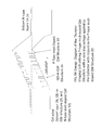
- potential signals V trans and ⁇ 2 can be supplied to the electrodes of the transfer gate 305 and the storage diode region 307 , respectively, in order to control (i.e., raise, lower and maintain) the potential barrier of the buried-QW-channel provided by the n-type modulation doped structure 32 between the imaging region 301 and the corresponding storage diode region 307 of each respective imaging cell and control electron current flow through this buried-QW-channel. More specifically, in the pixel setup mode of operation as shown in FIG.
- the potential signals V trans and ⁇ 2 are controlled to raise the potential barrier of the buried-QW-channel of the transfer gate 305 in order block electron current flow through this buried-QW-channel and thus isolate the imaging region 301 from the storage diode region 307 .
- the potential signals V trans and ⁇ 2 are controlled to lower the potential barrier of the buried-QW-channel of the transfer gate 305 in order produce a desired sub-threshold current flow through this buried-QW-channel to the storage diode region 307 for accumulation of charge arising from the electron photocurrent of the imaging region 301 in the storage diode region 307 .
- the surface potential of the buried-QW-channel of the transfer gate 305 is at or near the potential of electron charge that fills the buried-QW-channel of the imaging region 301 during pixel setup mode as described below.
- the electron charge that initially fills the imaging region i.e., the imaging region dark charge
- the potential signals V trans and ⁇ 2 are controlled to raise the potential barrier of the buried-QW-channel of the transfer gate 305 in order produce block reverse current flow through the buried-QW-channel back into the imaging region 301 of the imaging cell.
- a potential signal V out can be supplied to the electrode of the output gate 308 to control (i.e., raise, lower and maintain) the potential barrier of the buried-QW-channel provided by the n-type modulation doped structure 32 between the last storage diode region 307 and the output diode region 309 .
- control i.e., raise, lower and maintain
- Such control over the height of the potential barrier can be used to selectively control the conductivity of the buried-QW-channel of the output gate 308 .
- the potential signal V out can be controlled to raise the potential barrier of the buried-QW-channel of the output gate 308 in order to block electron current flow through this buried-QW-channel and thus isolate the last storage diode region 307 from the output diode region 309 .
- the potential signal V out can be controlled to lower the potential barrier of the buried-QW-channel of the output gate 308 in order to transfer the charge from the last storage diode region 307 to the output diode region 309 for output as a signal V signal .
- the signal V signal represents the accumulated charge for each respective imaging cell during read-out.
- the signal V signal is supplied to read-out circuitry for signal processing as desired.
- a reset gate 317 is disposed between the output diode region 309 and a reset diode region 319 .
- the reset diode region 319 can be formed by ion implantation of n-type species into a recess formed by etching down at least to the p-type layer 36 of device structure or other suitable techniques.
- the reset gate 317 can be realized by an elongate rib-like mesa that extends between the output diode region 309 and the reset diode region 319 .
- the reset gate 317 can have two opposed sidewalls that extend down to the output diode region 309 and to the reset diode region 319 , respectively.
- the reset gate 317 can also have two other sidewalls that are formed by etching down past the QW channel of the p-type modulation-doped QW structure 20 for isolation purposes.
- An electrode covers the top surface 38 of the elongate mesa of the reset gate 317 .
- the n-type modulation doped structure 32 provides a buried-QW-channel that allows for lateral transport of charge (i.e., electrons) through the reset gate 317 between the output diode region 309 and the reset diode region 319 .
- the reset diode region 319 is supplied with a potential bias signal (such as a V DD potential) that is configured to empty the storage diode regions 307 and output diode region 309 of all electrons.
- a potential signal V RS can be supplied to the electrode of the reset gate 317 to control (i.e., raise, lower and maintain) the potential barrier of the buried-QW-channel of the reset gate 317 .
- Such control over the height of the potential barrier can be used to selectively control the conductivity of the buried-QW-channel of the reset gate 317 .
- the potential signal V RS can be supplied to the electrode of the reset gate 317 to lower the potential barrier of the buried-QW-channel of the reset gate 317 in order to allow for electron charge transfer from the output diode region 309 to the reset diode region 319 (at V DD potential).
- the operation of the reset gate 317 can be operated in conjunction with register-to-register transfer of the CCD registers (barrier region 315 /storage diode region 307 pairs) carried out under control of the two phase clocking scheme ( ⁇ 1 and ⁇ 2) as well as in conjunction with operation of the output gate 308 in order to empty all of the storage diode regions 307 and the output diode region 309 of electrons and thus reset (i.e., clear) all of the storage diode regions 307 of the CCD register as well as the output diode region 309 .
- the potential signal V RS can be supplied to the electrode of the reset gate 317 to raise the potential barrier of the buried-QW-channel of the reset gate 317 in order to block charge transfer through this buried-QW-channel and thus isolate the output diode region 309 from the reset diode region 319 .
- a common input gate 311 is disposed between an input diode region 313 and the imaging regions 301 of the row of imaging cells.
- the input diode region 313 is realized by an elongate n-type doped region that extends parallel to the respective imaging regions 301 of the row of imaging cells.
- the input diode region 313 is supplied with a predetermined potential (e.g., ground potential) that is configured to populate the QW channel of the n-type modulation doped structure 32 of the imaging regions 301 of the imaging cells with electrons.
- the input diode region 313 can be formed by ion implantation of n-type species into a recess formed by etching down at least to the p-type layer 36 of device structure or other suitable techniques.
- the input gate 311 is realized by an elongate rib-like mesa that extends between the input diode region 313 and the respective imaging regions 301 of the row of imaging cells as evident from the cross-section of FIG. 3B .
- the input gate 311 has two opposed sidewalls that extend down to the input diode region 313 on one side and to the trench with doped region 304 adjacent the imaging regions 301 on the other side.
- the input gate 311 can also have two other sidewalls that are formed by etching down past the QW channel of the p-type modulation-doped QW structure 20 for isolation purposes.
- An electrode covers the top surface 38 of the elongate mesa of the input gate 311 .
- the n-type modulation doped structure 32 provides a buried-QW-channel that allows for lateral transport of charge (i.e., electrons) through the input gate 311 between the input diode region 313 and the imaging regions 301 of the row of imaging cells.
- a potential signal V in can be supplied to the electrode of the input gate 311 to control (i.e., raise, lower and maintain) the potential barrier of the buried-QW-channel of the input gate 311 between the input diode region 313 and the respective imaging regions 301 of the imaging cells.
- control i.e., raise, lower and maintain
- Such control over the height of the potential barrier can be used to selectively control the conductivity of the buried-QW-channel of the input gate 311 .
- the potential signal V in can be controlled to lower the potential barrier of the buried-QW-channel of the input gate 311 in order to allow for electron charge transfer from the input diode region 313 (at ground potential) to the imaging regions 301 .
- the predetermined potential e.g., ground potential
- the potential signal V in is controlled to raise the potential barrier of the buried-QW-channel of the input gate 311 in order to block electron charge transfer through this buried-QW-channel and thus isolate the input diode region 313 from the imaging regions 301 .
- FIG. 6 summarizes the current flow of the thyristor imaging cell during the signal integration mode operations for illustrate CCD-type imaging architecture of the embodiment of FIGS. 3A-3C (iv).
- the device structure is preferably subject to bias conditions where the thyristor action of the imaging regions 301 is OFF (a non-conducting state) as shown in the IV curve of FIG. 7 .
- These bias conditions form a depletion region that encompasses the QD-in-QW structure 28 of the respective imaging regions 301 and moves electrons from the n-type delta doping of the QD-in-QW structure 28 into the QDs of the QD-in-QW structure 28 of the respective imaging regions 301 .
- bias conditions also introduce a relatively small electron diffusion current from the n-type modulation doped QW structure 28 into the QDs of the QD-in-QW structure 28 of the respective imaging regions 301 .
- electrons are supplied to the QDs of the QD-in-QW structure 28 of the respective imaging regions 301 .
- the QDs of the QD-in-QW structure 28 are subject to a built-in electric field that moves mobile electrons toward the n-type modulation doped QW structure 28 of the respective imaging regions 301 .
- the electrons in the QDs will receive enough energy to place them in the conduction band via intersubband transitions.
- the built-in electric field moves the mobile electrons to the QW channel of the n-type modulation doped QW structure 32 of the respective imaging regions 301 .
- the intersubband absorption mechanism of the QDs of the QD-in-QW structure 28 produces electron photocurrent that flows to the QW channel of the n-type modulation doped QW structure 32 under the influence of the built-in electric field of device structure.
- the n-type modulation doped QW structure 32 provides a buried-QW-channel that allows for lateral transport of electron photocurrent from the respective imaging regions 301 to respective storage diode regions 307 of the row of the imaging cells.
- the electron charge resulting from such photocurrent accumulates in respective storage diode regions 307 of the imaging cells over the time period of the signal integration mode.
- the amount of accumulated charge for the imaging cell is proportional to the power of the incident electromagnetic radiation at the characteristic wavelength absorbed by the QDs of the QD-in-QW structure 28 that is received at the imaging cell during the signal integration period.
- the imaging cells of the illustrative CCD-type imaging architecture preferably operate over successive imaging cycles that include the three distinct modes as described above: a pixel setup mode; a signal integration mode; and a readout mode.
- the potential V trans of the transfer gate 305 is controlled to block electron charge transfer through the buried-QW-channel of the transfer gate 305 and thus isolate the imaging region 301 from corresponding storage diode regions 307 of the imaging cells.
- the potential V IN of the input gate 311 is then controlled to lower the potential barrier of the input gate 311 .
- the potential V IN of the input gate 311 is then controlled to raise the potential barrier in order to block electron charge transfer through the buried-QW-channel of the input gate 311 and thus isolate the input diode region 313 from the imaging regions 301 of the imaging cells.
- the potential V RS of the reset gate 317 is controlled to lower the potential barrier of the reset gate 317 in order to allow for electron charge transfer from the output diode region 309 to the reset diode region 319 (at V DD potential).
- the operation of the reset gate 317 can be operated in conjunction with register-to-register transfer of the CCD registers (barrier region 315 /storage diode region 307 pairs) carried out under control of the two phase clocking scheme ( ⁇ 1 and ⁇ 2) as well as in conjunction with operation of the output gate 308 in order to empty all of the storage diode regions 307 and the output diode region 309 of electrons and thus reset (i.e., clear) all of the storage diode regions 307 of the CCD register as well as the output diode region 309 .
- the potential V RS of the reset gate 317 is then controlled to raise the potential barrier and isolate the reset diode region 319 .
- the potential V IN of the input gate 311 remains at the level that blocks electron charge transfer through the buried-QW-channel of the input gate 311 and thus isolates the input diode region 313 from the imaging regions 301 of the imaging cells.
- the potential signals V trans and ⁇ 2 of the transfer gates 305 and the storage diode regions 307 are controlled to lower the potential barrier of the buried-QW-channel of the transfer gates 305 in order produce a desired subthreshold current flow through this buried-QW-channel to the respective storage diode regions 307 .
- the electron photocurrent that results from absorption in the QDs of the QD-in-QW structure 28 of the imaging cells flows through the buried-QW-channels and accumulates in the respective storage diode regions 307 .
- the amount of accumulated charge in each respective storage diode region 307 is proportional to the power of the incident electromagnetic radiation at the characteristic absorption wavelength of the QDs of the of the QD-in-QW structure 28 that is received at the imaging cell during the signal integration period.
- the potential signal V trans of the transfer gate 305 is controlled to raise the potential barrier of the buried-QW-channel of the transfer gate 305 in order to block electron charge transfer through the buried-QW-channel of the input gate transfer gate and thus isolate the imaging regions 301 from the storage diode regions 307 of the imaging cells.
- register-to-register transfer of the CCD registers is carried out under control of the two phase clocking scheme ( ⁇ 1 and ⁇ 2) in order to transfer the accumulated charge (i.e., electrons) between the storage diode regions 307 to the last storage diode region 307 of the CCD registers of the row while controlling the potential of the output gate 308 to transfer the charge from the last storage region 307 to the output diode region 309 for output as a signal V signal .
- the signal V signal which represents the accumulated charge for each respective imaging cell during readout and is proportional to the power of the incident electromagnetic radiation at the characteristic absorption wavelength of the QDs of the of the QD-in-QW structure 28 that is received at the imaging cell during the signal integration period.
- the signal V signal is supplied to read-out circuitry for signal processing as desired.
- the thyristor imaging cells can also be part of an active-pixel-type imaging architecture as shown in the illustrative embodiment of FIGS. 5A-5C (iv).
- a linear array (row) of thyristor imaging cells is made utilizing the layer structure of FIGS. 1 to 2B .
- Multiple rows of thyristor imaging cells can be formed to provide a two-dimensional imaging array as desired.
- Each thyristor imaging cell includes an imaging region 301 defined by a mesa that includes a top (anode) terminal 101 formed adjacent the highly doped top p-type ohmic contact layer 38 .
- a bottom (cathode) terminal 103 is operably coupled to the bottom n-type ohmic contact layer 14 that is common to the imaging cells of the array.
- the mesa of the imaging region 301 is defined by opposed trenches that extend downward at least to the p-type layer 36 of device structure and form sidewalls of the corresponding transfer output gate 305 and the common input gate 311 .
- the other two sidewalls of the mesa are formed by etching down past the QW channel of the p-type modulation-doped QW structure 20 for isolation between the imaging regions 301 of the row of imaging regions 301 .
- the sidewalls of the mesa provide for lateral confinement of the electromagnetic radiation within the imaging region 301 .
- the lateral extent of the mesa can vary by design. In one embodiment, the lateral extent of the mesa covers an area on the order of 30 ⁇ m by 1 ⁇ m.
- the layer structure between the top p-type ohmic contact layer 38 and the bottom n-type ohmic contact layer 14 of the mesa of the imaging region 301 defines a vertical thyristor (P-N-P-N) structure.
- N-type doped regions 304 are formed at the bottom of the two trenches as shown. The doped regions 304 can be formed by ion implantation of an n-type species as desired or other suitable technique.
- a portion of the top surface of the mesa of each respective imaging region 301 is not covered by the top anode terminal 101 to form respective apertures 303 into the device structure of the imaging regions 301 .
- the top DBR mirror 40 can be formed continuously across the integrated circuit structure and covers the apertures 303 as shown.
- the top DBR mirror 40 and the bottom DBR mirror 12 together form a resonant cavity with the device structure of the respective imaging regions 301 therebetween. For each imaging cell, incident electromagnetic radiation passes through the top DBR mirror 40 (and aperture 303 ) into this resonant cavity for absorption in the respective imaging region 301 .
- the QW channel of the n-type modulation doped QW structure 32 of each respective imaging region 301 is initialized such that it is at or near ground potential and filled with majority carrier electrons, and the bias potential of the device structure is set via bias potential signals supplied to the top anode terminal 101 (e.g., V image of 1 volt) and to the bottom cathode terminal 103 (e.g., 0.5V) such that a positive bias potential is applied to a collector underlying the n-type modulation doped QW structure 32 with respect to the n-type modulation doped QW structure 32 of the respective imaging regions.
- the collector includes spacer layer 26 , QD-in-QW structure 24 and the p-type modulation doped QW structure 20 .
- bias conditions form a depletion region that encompasses the QD-in-QW structure 28 and moves electrons from n-type delta doping of the QD-in-QW structure 28 into the QDs of the QD-in-QW structure 32 of the respective imaging regions 301 .
- the bias conditions also introduce a relatively small electron diffusion current that flows vertically from the n-type modulation doped QW structure 32 toward the collector in the respective imaging regions 301 . This diffusion current also supplies electrons to the QDs of the QD-in-QW structure 28 in the respective imaging regions 301 .
- This electron diffusion current has a magnitude that is smaller than the expected electron photocurrent induced by absorption of electromagnetic radiation by the QDs of the QD-in-QW structure 28 in the respective imaging regions 301 .
- the n-type modulation doped QW structure 32 provides a buried-QW-channel on one side of the respective imaging regions 301 that extends through a series of device structures for each respective imaging cell, including a transfer gate 305 , a storage diode region 307 ′, an output gate 308 ′ and an output diode region 309 ′.
- This buried-QW-channel allows for lateral transport of electron photocurrent from the respective imaging regions 301 to respective storage diode regions 307 ′ of the imaging cells via corresponding transfer gates 305 during signal integration as well as lateral transport of accumulated electron charge from the respective storage diode regions 307 ′ to the output diode regions 309 ′ during readout operations as described below in more detail.
- the transfer gate 305 , the storage diode region 307 ′ and the output gate 308 ′ are realized by mesas with trenches and doped regions 304 therebetween.
- the sidewalls of the trenches extend downward at least to the p-type layer 36 of device structure as best shown in FIG. 5B .
- the mesas of the transfer gate 305 , the storage diode region 307 ′ and the output gate 308 ′ also have opposed sidewalls (not shown in the cross-section of FIG. 5B ) that are formed by etching down past the QW channel of the p-type modulation-doped QW structure 20 for isolation between the transfer gates 305 of the row of imaging cells.
- An electrode (V trans ) covers the top surface 38 of the mesa of the transfer gate 305
- an electrode ( ⁇ 2) covers the top surface 38 of the mesa of the storage diode region 307 ′
- an electrode (V out ) covers the top surface 38 of the mesa of the storage output gate 308 ′ as best shown in FIG. 5B .
- the output diode region 309 ′ can be formed by ion implantation of n-type species into a recess formed by etching down at least to the p-type layer 36 of device structure or other suitable techniques.
- potential signals V trans and V storage can be supplied to the electrodes of the transfer gate 305 and the storage diode region 307 ′, respectively, in order to control (i.e., raise, lower and maintain) the potential barrier of the buried-QW-channel provided by the n-type modulation doped structure 32 between the imaging region 301 and the corresponding storage diode region 307 ′ of each respective imaging cell and control electron current flow through this buried-QW-channel. More specifically, in the pixel setup mode of operation as shown in FIG.
- the potential signals V trans and V storage are controlled to raise the potential barrier of the buried-QW-channel of the transfer gate 305 in order block electron current flow through this buried-QW-channel and thus isolate the imaging region 301 from the storage diode region 307 ′.
- the potential signals V trans and V storage are controlled to lower the potential barrier of the buried-QW-channel of the transfer gate 305 in order produce a desired sub-threshold current flow through this buried-QW-channel to the storage diode region 307 ′ for accumulation of charge arising from the electron photocurrent of the imaging region 301 in the storage diode region 307 ′.
- the surface potential of the buried-QW-channel of the transfer gate 305 is at or near the potential of electron charge that fills the buried-QW-channel of the imaging region 301 during pixel setup mode as described below.
- the electron charge that initially fills the imaging region i.e., the imaging region dark charge
- the potential signals V trans and V storage are controlled to raise the potential barrier of the buried-QW-channel of the transfer gate 305 in order produce block reverse current flow through the buried-QW-channel back into the imaging region 301 of the imaging cell.
- FIGS. 5D-5F (iv) illustrates an alternate embodiment employing and active-pixel type imaging architecture wherein the function of the transfer gate and charge storage region of the embodiment of FIGS. 5A-5C (iv) are combined in a transfer and storage gate 307 ′′.
- an undoped barrier region 320 and doped charge storage region 321 are disposed adjacent one another under a common electrode (V transfer/storage ) with the undoped barrier region 320 located between the imaging region 301 and the doped charge storage region 321 .
- the n-type modulation doped structure 32 provides a buried-QW-channel that allows for lateral transport of electron photocurrent from the respective imaging region 301 to the doped charge storage region 321 of the imaging cell.
- the storage diode region 321 can be realized by an n-type doped region that is configured as a potential well that accumulates charge (i.e., electrons) arising from the electron photocurrent produced in the corresponding imaging region 301 during imaging operations.
- the undoped barrier region 320 has a positive built-in potential relative to the n-doped charge storage regions 321 in order to provide a built-in barrier to electron current flow.
- An electrode (V transfer/storage ) covers the top surface 38 of the transfer and storage gate 307 ′′ as best shown in 5 E.
- a potential signal V transfer/storage can be supplied to the electrode of the transfer and storage gate 307 ′′ in order to control (i.e., raise, lower and maintain) the potential barrier of the buried-QW-channel provided by the n-type modulation doped structure 32 between the imaging region 301 and the corresponding storage diode region 321 of the respective thyristor imaging cell and control electron current flow through this buried-QW-channel. More specifically, in the pixel setup mode of operation as shown in FIG.
- the potential signal V transfer/storage is controlled to raise the potential barrier of the buried-QW-channel of the transfer and storage gate 307 ′′ in order to block electron current flow through this buried-QW-channel and thus isolate the imaging region 301 from the storage diode region 321 .
- the potential signal V transfer/storage is controlled to lower the potential barrier of the buried-QW-channel of the transfer and storage gate 307 ′′ in order to produce a desired subthreshold current flow through this buried-QW-channel to the respective charge storage region 321 for accumulation of charge arising from the electron photocurrent of the imaging region 301 in the charge storage region 321 .
- the surface potential of the buried-QW-channel of the undoped barrier region 320 is at or near the potential of electron charge that fills the QW of the n-type modulation doped QW structure 32 of the imaging region 301 during pixel setup mode as described below.
- the electron charge that initially fills the imaging region i.e., the imaging region dark charge
- the potential barrier provided by the undoped barrier region 320 blocks reverse current flow through the buried-QW-channel of the transfer and storage gate 307 ′′ back into the imaging region 301 of the imaging cell.
- a common input gate 311 is disposed between an input diode region 313 and the imaging regions 301 of the row of imaging cells.
- the input diode region 313 is realized by an elongate n-type doped region that extends parallel to the respective imaging regions 301 of the row of imaging cells.
- the input diode region 313 is supplied with a predetermined potential (e.g., ground potential) that is configured to populate the QW channel of the n-type modulation doped structure 32 of the imaging regions 301 of the imaging cells with electrons.
- the input diode region 313 can be formed by ion implantation of n-type species into a recess formed by etching down at least to the p-type layer 36 of device structure or other suitable techniques.
- the input gate 311 is realized by an elongate rib-like mesa that extends between the input diode region 313 and the respective imaging regions 301 of the row of imaging cells as evident from the cross-section of FIG. 3B .
- the input gate 311 has two opposed sidewalls that extend down to the input diode region 313 on one side and to the trench with doped region 304 adjacent the imaging regions 301 on the other side.
- the input gate 311 can also have two other sidewalls that are formed by etching down past the QW channel of the p-type modulation-doped QW structure 20 for isolation purposes.
- An electrode covers the top surface 38 of the elongate mesa of the input gate 311 .
- the n-type modulation doped structure 32 provides a buried-QW-channel that allows for lateral transport of charge (i.e., electrons) through the input gate 311 between the input diode region 313 and the imaging regions 301 of the row of imaging cells.
- charge i.e., electrons
- a potential signal V in can be supplied to the electrode of the input gate 311 to control (i.e., raise, lower and maintain) the potential barrier of the buried-QW-channel of the input gate 311 between the input diode region 313 and the respective imaging regions 301 of the imaging cells.
- control i.e., raise, lower and maintain
- Such control over the height of the potential barrier can be used to selectively control the conductivity of the buried-QW-channel of the input gate 311 .
- the potential signal V in can be controlled to lower the potential barrier of the buried-QW-channel of the input gate 311 in order to allow for electron charge transfer from the input diode region 313 (at ground potential) to the imaging regions 301 .
- the predetermined potential e.g., ground potential
- the potential signal V in is controlled to raise the potential barrier of the buried-QW-channel of the input gate 311 in order to block electron charge transfer through this buried-QW-channel and thus isolate the input diode region 313 from the imaging regions 301 .
- the n-type modulation doped structure 32 also provides a buried-QW-channel that couples the storage diode region 307 ′ to the output diode region 309 ′ via the corresponding output gate 308 ′.
- the n-type modulation doped structure 32 also provides a buried-QW-channel that couples the charge storage region 321 of the transfer and storage gate 307 ′′ to the output diode region 309 ′ via the corresponding output gate 308 ′.
- a potential signal V out can be supplied to the electrode of the output gate 308 ′ to control (i.e., raise, lower and maintain) the potential barrier of the buried-QW-channel provided by the n-type modulation doped structure 32 between the storage diode region 307 ′ or 321 and the output diode region 309 ′.
- control over the height of the potential barrier can be used to selectively control the conductivity of the buried-QW-channel of the output gate 308 ′.
- the potential signal V out can be controlled to raise the potential barrier of the buried-QW-channel of the output gate 308 ′ in order to block electron current flow through this buried-QW-channel and thus isolate the storage diode region 307 ′ or 321 from the output diode region 309 ′.
- the potential signal V out can be controlled to lower the potential barrier of the buried-QW-channel of the output gate 308 ′ in order to transfer the charge from the storage diode region 307 ′ or 321 to the output diode region 309 ′ for output as a signal V signal .
- the signal V signal represents the accumulated charge for each respective imaging cell during read-out.
- each imaging cell employs three transistors: a reset transistor (labeled “RST”), a source follower (labeled “SRC”) and a row select transistor (labeled “SEL).
- RST reset transistor
- SRC source follower
- SEL row select transistor
- the row select transistor is turned OFF and the reset transistor is turned ON to electrically couple the output diode region 309 ′ of the corresponding imaging cell to a fixed potential (such as V DD ) that empties the output diode region 309 ′ of electrons and thus resets the output diode region 309 ′ of the corresponding imaging cell.
- the reset transistor is turned OFF to electrically isolate the output diode region 309 ′ of the corresponding imaging cell from the fixed potential (such as V DD ), the row select transistor is turned OFF, and the source follower transistor generates a voltage signal corresponding to the charge level of electrons accumulated in the output diode region 309 ′ during the signal integration mode.
- the reset transistor is turned OFF to electrically isolate the output diode region 309 ′ of the corresponding imaging cell from the fixed potential (such as V DD ) and the row select transistor (labeled “SEL) is turned ON to output the voltage signal V signal generated by the source follower transistor onto the corresponding column bus for the array of imaging cells.
- the signal V signal represents the accumulated charge for each respective imaging cell during readout and is proportional to the power of the incident electromagnetic radiation at the characteristic wavelength absorbed by the QDs of the QD-in-QW structure 28 that is received at the imaging cell during the signal integration period.
- the signal V signal is supplied to read-out circuitry for signal processing as desired.
- FIG. 6 summarizes the current flow of the thyristor imaging cell during the signal integration mode operations for the active-pixel-type imaging architecture of the embodiment of FIGS. 5A-5C (iv) and 5 D- 5 F(iv).
- the device structure is preferably subject to bias conditions where the thyristor action of the imaging region 301 is OFF (a non-conducting state) as shown in the IV curve of FIG. 7 .
- These bias conditions form a depletion region that encompasses the QD-in-QW structure 28 of the respective imaging regions 301 and moves electrons from the n-type delta doping of the QD-in-QW structure 28 into the QDs of the QD-in-QW structure 28 of the respective imaging regions 301 .
- bias conditions also introduce a relatively small electron diffusion current from the n-type modulation doped QW structure 28 into the QDs of the QD-in-QW structure 28 of the respective imaging regions. In this manner, electrons are supplied to the QDs of the QD-in-QW structure 28 of the respective imaging regions 301 .
- the QDs of the QD-in-QW structure 28 are subject to a built-in electric field that moves mobile electrons toward the n-type modulation doped QW structure 28 of the respective imaging regions 301 .
- the electrons in the QDs will receive enough energy to place them in the conduction band via intersubband transitions.
- the built-in electric field moves the mobile electrons to the QW channel of the n-type modulation doped QW structure 32 of the respective imaging regions 301 .
- the intersubband absorption mechanism of the QDs of the QD-in-QW structure 28 produces electron photocurrent that flows to the QW channel of the n-type modulation doped QW structure 32 under the influence of the built-in electric field of device structure.
- the n-type modulation doped QW structure 32 provides a buried-QW-channel that allows for lateral transport of electron photocurrent from the respective imaging regions 301 to respective storage diode regions 307 ′ (or the charge storage regions 321 ) of the row of the imaging cells.
- the electron charge resulting from such photocurrent accumulates in respective storage diode regions 307 ′ (or in the charge storage regions 321 ) of the imaging cells over the time period of the signal integration mode.
- the amount of accumulated charge for the imaging cell is proportional to the power of the incident electromagnetic radiation at the characteristic wavelength absorbed by the QDs of the QD-in-QW structure 28 that is received at the imaging cell during the signal integration period.
- the imaging cells of the illustrative active-pixel-type imaging architecture preferably operate over successive imaging cycles that include the three distinct modes as described above: a pixel setup mode; a signal integration mode; and a readout mode.
- the potential V trans of the transfer gate 305 (or the potential V transfer/storage of the transfer/storage gate 307 ”) of each respective imaging cell is controlled to block electron charge transfer through the buried-QW-channel of the transfer gate 305 (or through the transfer/storage gate 307 ′′) and thus isolate the imaging region 301 from corresponding storage diode region 307 or 321 of the respective imaging cell.
- the potential V IN of the input gate 311 is then controlled to lower the potential barrier of the input gate 311 .
- the potential V IN of the input gate 311 is then controlled to raise the potential barrier in order to block electron charge transfer through the buried-QW-channel of the input gate 311 and thus isolate the input diode region 313 from the imaging regions 301 of the imaging cells.
- the potential V out of the output gate 308 ′ of each respective imaging cell is controlled to raise the potential barrier of the output gate 308 ′ in order to block electron charge transfer through the buried-QW-channel of the output gate 308 ′ and thus isolate the storage diode region 307 or 321 from the corresponding output diode region 309 ′ of the respective imaging cell.
- the row select transistor is turned OFF and the reset transistor is turned ON to electrically couple the output diode region 309 ′ of the corresponding imaging cell to a fixed potential (such as V DD ) that empties the output diode region 309 ′ of electrons and thus resets the output diode region 309 ′ of the respective imaging cell.
- the potential V IN of the input gate 311 remains at the level that blocks electron charge transfer through the buried-QW-channel of the input gate 311 and thus isolates the input diode region 313 from the imaging regions 301 of the imaging cells.
- the potential V out of the output gate 308 ′ remains at the level that isolates the storage diode region 307 ′ (or the charge storage region 321 ) from the output diode region 309 ′ of the respective imaging cell.
- the potential signals V trans and V storage of the transfer gate 305 and the storage diode region 307 ′ of each respective imaging cell are controlled to lower the potential barrier of the transfer gate 305 in order produce a desired subthreshold current flow through this buried-QW-channel to the respective storage diode regions 307 ′.
- the electron photocurrent that results from absorption in the QDs of the QD-in-QW structure 28 of the imaging cells flows through the buried-QW-channels and accumulates in the respective storage diode regions 307 ′.
- each respective storage diode region 307 ′ is proportional to the power of the incident electromagnetic radiation at the characteristic absorption wavelength of the QDs of the of the QD-in-QW structure 28 that is received at the imaging cell during the signal integration period.
- the potential signal V transfer/storage of the transfer/storage gate 307 ′′ of each respective imaging cell is controlled to lower the potential barrier of the buried-QW-channel provided by the transfer/storage gate 307 ′′ in order produce a desired subthreshold current flow through this buried-QW-channel to the respective charge storage regions 321 .
- the electron photocurrent that results from absorption in the QDs of the QD-in-QW structure 28 of the imaging cells flows through the buried-QW-channels and accumulates in the respective charge storage region 321 .
- the amount of accumulated charge in each respective charge storage region 321 is proportional to the power of the incident electromagnetic radiation at the characteristic absorption wavelength of the QDs of the of the QD-in-QW structure 28 that is received at the imaging cell during the signal integration period.
- the reset transistor of each respective imaging cell is turned OFF to electrically isolate the output diode region 309 ′ of the imaging cell from the fixed potential (such as V DD ), and the row select transistor of the respective imaging cell is turned OFF.
- the potential signal V out supplied to the output gate 308 ′ of each respective imaging cell can be controlled to lower the potential barrier of the buried-QW-channel of the output gate 308 ′ in order to transfer the charge from the storage diode region 307 ′ (or the charge storage region 321 ) to the output diode region 309 ′, which controls the source follower transistor (SRC) of the imaging cell to output a signal V signal .
- SRC source follower transistor
- the reset transistor of each respective imaging cell is turned OFF to electrically isolate the output diode region 309 ′ of the imaging cell from the fixed potential (such as V DD ), and the row select transistor (labeled “SEL) of each respective imaging cell is turned ON to output the signal V signal generated by the source follower transistor onto the corresponding column bus for the array of imaging cells.
- the signal V signal represents the accumulated charge for each respective imaging cell during readout and is proportional to the power of the incident electromagnetic radiation at the characteristic absorption wavelength of the QDs of the of the QD-in-QW structure 32 that is received at the imaging cell during the signal integration period.
- the signal V signal is supplied to read-out circuitry for signal processing as desired.
- the thyristor imaging cells can also be part of a CCD-type imaging architecture for dual wavelength imaging as shown in the illustrative embodiment of FIGS. 8A-8C (viii).
- a linear array (row) of thyristor imaging cells is made utilizing the layer structure of FIGS. 1 to 2B .
- Multiple rows of thyristor imaging cells can be formed to provide a two-dimensional imaging array as desired.
- Each thyristor imaging cell includes an imaging region 301 defined by a mesa that includes a top (anode) terminal 101 formed adjacent the highly doped top p-type ohmic contact layer 38 .
- a bottom (cathode) terminal 103 is operably coupled to the bottom n-type ohmic contact layer 14 .
- the mesa of the imaging region 301 is defined by two opposed trenches. One of the two trenches extends down to at least the p-type layer 36 of device structure adjacent the corresponding transfer gate 305 - 1 , and the other trench extends down at or near the p-type modulation-doped QW structure 20 adjacent the corresponding transfer gate 305 - 2 .
- the other two sidewalls of the mesa (not shown in the cross-sections of FIG.
- the sidewalls of the mesa provide for lateral confinement of the electromagnetic radiation within the imaging region 301 .
- the lateral extent of the mesa can vary by design. In one embodiment, the lateral extent of the mesa covers an area on the order of 30 ⁇ m by 1 ⁇ m.
- An n-type doped region 304 is formed at the bottom of the trench adjacent the common output gate 305 - 1 .
- a p-type doped region 351 is formed at the bottom of the trench adjacent the corresponding transfer gate 305 - 2 .
- the doped regions 304 , 351 can be formed by ion implantation of an n-type and p-type species as desired or other suitable technique.
- the layer structure between the top p-type ohmic contact layer 38 and the bottom n-type ohmic contact layer 14 of the mesa of the imaging region 301 defines a vertical thyristor (P-N-P-N) structure.
- a portion of the mesa of each respective imaging region 301 is not covered by the top anode terminal 101 to form respective apertures 303 into the device structure for the imaging regions 301 .
- the top DBR mirror 40 can be formed continuously across the integrated circuit structure and covers the aperture 303 as shown.
- the top DBR mirror 40 and the bottom DBR mirror 12 together form a resonant cavity with the device structure of the imaging regions 301 therebetween.
- the vertical dimension of the resonant cavity is configured to correspond to the characteristic wavelength band of absorption of the QDs of the QD structure 24 as well to the characteristic wavelength band of absorption of the QDs of the QD structure 28 .
- the thickness of the layers of the top DBR mirror 40 and the bottom DBR mirror 12 are selected to reflect electromagnetic radiation within characteristic wavelength range of absorption of the QDs of both the QD structure 24 and the QD structure 20 . Incident electromagnetic radiation passes through the top DBR mirror 40 (and aperture 303 ) into this resonant cavity for absorption.
- the QW channel of the n-type modulation doped QW structure 32 of each respective imaging region 301 is initialized such that it is at or near ground potential and filled with majority carrier electrons
- the QW channel of the p-type modulation doped QW structure 20 of each respective imaging region 301 is initialized such that it is at or near V DD potential and filled with majority carrier holes
- a positive bias potential is applied to a first collector region underlying the n-type modulation doped QW structure 32 with respect to the n-type modulation doped QW structure 32 of the respective imaging regions 301 .
- the first collector region includes spacer layer 26 , QD-in-QW structure 24 and the p-type modulation doped QW structure 20 .
- a negative bias potential is applied to a second collector region overlying the p-type modulation doped QW structure 20 with respect to the p-type modulation doped QW structure 20 of the respective imaging regions 301 .
- the second collector region includes spacer layer 26 , QD-in-QW structure 28 and the n-type modulation doped QW structure 32 .
- bias conditions form a first depletion region that encompasses the QD-in-QW structure 28 and moves electrons from the n-type delta doping of the QD-in-QW structure 28 into the QDs of the QD-in-QW structure 28 of the respective imaging regions 301 as well as a second depletion region that encompasses the QD-in-QW structure 24 and moves holes from the p-type delta doping of the QD-in-QW structure 24 into the QDs of the QD-in-QW structure 24 of the respective imaging regions 301 .
- These bias conditions also introduce a relatively small electron diffusion current that flows vertically from the n-type modulation doped QW structure 32 toward the first collector region in the respective imaging regions 301 .
- This electron diffusion current supplies electrons to the QDs of the QD-in-QW structure 28 in the respective imaging regions 301 .
- This electron diffusion current has a magnitude that is smaller than the expected electron photocurrent induced by absorption of electromagnetic radiation by the QDs of the QD-in-QW structure 28 in the respective imaging regions 301 .
- the bias conditions introduce a relatively small hole diffusion current that flows vertically from the p-type modulation doped QW structure 20 toward the second collector region in the respective imaging regions 301 .
- This hole diffusion current supplies holes to the QDs of the QD-in-QW structure 24 in the respective imaging regions 301 .
- This hole diffusion current has a magnitude that is smaller than the expected hole photocurrent induced by absorption of electromagnetic radiation by the QDs of the QD-in-QW structure 24 in the respective imaging regions 301 .
- the bias conditions for the n-type modulation doped QW structure 32 and the first collector region are similar to that discussed above with respect to FIGS. 4A and 4B .
- the bias conditions for the p-type modulation doped QW structure 20 and the second collector region are shown in the energy diagrams of FIGS. 9A and 9B .
- FIG. 9A shows an exemplary energy diagram for a zero bias voltage the second collector region and the p-type modulation doped structure 20 .
- FIG. 9B shows an exemplary energy diagram for a negative bias potential is applied to the second collector region with respect to the p-type modulation doped QW structure 20 .
- the QDs of the QD-in-QW structure 24 in a given imaging region 301 are in the depletion region of the second collector region, which is subject to a built-in electric field that moves mobile holes toward the p-type modulation doped QW structure 20 of the imaging region 301 .
- the holes in the QDs will receive enough energy to place them in the valence band via intersubband transitions.
- the built-in electric field moves the mobile holes to the QW channel of the p-type modulation doped QW structure 20 of the imaging region 301 .
- the intersubband absorption mechanism of the QDs of the QD-in-QW structure 24 produces hole photocurrent that flows to the QW channel of the p-type modulation doped layer 20 under the influence of the built-in electric field of device structure.
- the bias conditions produce an applied electric field in an opposite sense to built-in electric field in order to provide for the desired diffusion current of the majority carrier holes from the QW channel of the p-type modulation doped QW structure 20 to the QDs of the QD-in-QW structure 24 in the imaging region 301 .
- the n-type modulation doped QW structure 32 provides a buried-QW-channel that allows for lateral transport of electron photocurrent from the respective imaging regions 301 to respective storage diode regions 307 - 1 of the row of imaging cells via corresponding transfer gates 305 - 1
- the p-type modulation doped QW structure 20 provides a buried-QW-channel that allows for lateral transport of hole photocurrent from the respective imaging regions 301 to respective storage diode regions 307 - 2 of the row of the thyristor imaging cells via corresponding transfer gates 305 - 2 .
- the storage diode regions 307 - 1 are realized by n-type doped regions that accumulate charge (i.e., electrons) that arises from the electron photocurrent produced in the corresponding imaging region 301 during operation.
- the storage diode regions 307 - 2 are realized by p-type doped regions that accumulate charge (i.e., electrons) that arises from the hole photocurrent produced in the corresponding imaging region 301 during operation.
- the storage diode regions 307 - 1 and 307 - 2 can be formed by ion implantation of n-type species or p-type species as desired or other suitable techniques.
- the transfer gates 305 - 1 and 305 - 2 are each realized by structures that extend between the respective imaging regions 301 and the respective storage diode regions 307 - 1 and 307 - 2 on opposite sides of the row of the imaging cells.
- the transfer gates 305 - 1 and storage diode regions 307 - 1 are similar to the transfer gates 305 and storage diode regions 307 of the embodiment described above with respect to FIGS. 3A-3C (iv).
- the transfer gates 305 - 2 and storage diode regions 307 - 2 are also similar in structure to the transfer gates 305 and storage diode regions 307 of the embodiment described above with respect to FIGS. 3A-3C (iv); however, they are formed into intermediate layers of the device layer structure of FIGS.
- potential signals V trans-n and ⁇ 2-n can be supplied to the electrodes of the transfer gate 305 - 1 and the storage diode region 307 - 1 , respectively, in order to control (i.e., raise, lower and maintain) the potential barrier of the buried-QW-channel of the transfer gate 305 - 1 in order to control current flow this buried-QW-channel. More specifically, in the pixel setup mode of operation as shown in FIG.
- the potential signals V trans-n and ⁇ 2-n are controlled to raise the potential barrier of the buried-QW-channel provided by the transfer gate 305 - 1 in order to block current flow through this buried-QW-channel and isolate the imaging region 301 from the storage diode region 307 - 1 .
- the signal integration mode of operation as shown in FIG.
- the potential signals V trans-n and ⁇ 2-n are controlled to lower the potential barrier of the buried-QW-channel of the transfer gate 305 - 1 in order produce a desired subthreshold electron current flow through this buried-QW-channel to the respective storage diode region 307 - 1 for accumulation of charge arising from the electron photocurrent of the imaging region 301 in the storage diode region 307 - 1 .
- the surface potential of the buried-QW-channel of the transfer gate 305 - 1 is at or near the potential of electron charge that fills the QW of the n-type modulation doped QW structure 32 of the imaging region 301 during pixel setup mode as described below.
- the electron charge that initially fills the imaging region i.e., the imaging region dark charge
- the electron charge that initially fills the imaging region is blocked from flowing through the buried-QW-channel of the transfer gate 305 - 1 while allowing for the electron photocurrent arising from absorption in the imaging region 301 to flow over this potential barrier and through the buried-QW-channel of the transfer gate 305 - 1 for accumulation in the storage diode region 307 - 1 of the imaging cell.
- the potential signals V trans-n and ⁇ 2-n are controlled to raise the potential barrier of the buried-QW-channel of the transfer gate 305 - 1 in order produce block reverse current flow through the buried-QW-channel of the transfer gate 305 - 1 back into the imaging region 301 of the imaging cell.
- potential signals V trans-p and ⁇ 2-p can be supplied to the electrodes of the transfer gate 305 - 2 and the storage diode region 307 - 12 respectively, in order to control (i.e., raise, lower and maintain) the potential barrier of the buried-QW-channel of the transfer gate 305 - 2 in order to control current flow this buried-QW-channel. More specifically, in the pixel setup mode of operation as shown in FIG.
- the potential signals V trans-p and ⁇ 2-p are controlled to raise the potential barrier of the buried-QW-channel provided by the transfer gate 305 - 2 in order to block current flow through this buried-QW-channel and isolate the imaging region 301 from the storage diode region 307 - 2 .
- the signal integration mode of operation as shown in FIG.
- the potential signals V trans-p and ⁇ 2-p are controlled to lower the potential barrier of the buried-QW-channel of the transfer gate 305 - 3 in order produce a desired subthreshold hole current flow through this buried-QW-channel to the respective storage diode region 307 - 2 for accumulation of charge arising from the hole photocurrent of the imaging region 301 in the storage diode region 307 - 2 .
- the surface potential of the buried-QW-channel of the transfer gate 305 - 2 is at or near the potential of hole charge that fills the QW of the p-type modulation doped QW structure 20 of the imaging region 301 during pixel setup mode as described below.
- the hole charge that initially fills the imaging region i.e., the imaging region dark charge
- the hole charge that initially fills the imaging region is blocked from flowing through the buried-QW-channel of the transfer gate 305 - 2 while allowing for the hole photocurrent arising from absorption in the imaging region 301 to flow over this potential barrier and through the buried-QW-channel of the transfer gate 305 - 2 for accumulation in the storage diode region 307 - 2 of the imaging cell.
- the potential signals V trans-p and ⁇ 2-p are controlled to raise the potential barrier of the buried-QW-channel provided by the p-type modulation doped structure 32 between the imaging region 301 and the storage diode region 307 - 2 in order produce block reverse current flow through the buried-QW-channel of the transfer gate 305 - 2 back into the imaging region 301 of the imaging cell.
- the storage diode regions 307 - 1 are disposed adjacent corresponding barrier regions 315 - 1 .
- the storage diode region 307 - 1 and barrier region 315 - 1 pairs realize a top row of CCD registers similar to the embodiment of FIGS. 3A-3C (iv) that operates under control of a two phase clocking scheme ( ⁇ 1 and ⁇ 2) to transfer charge (i.e., electrons) register-to-register to the last storage diode region 307 - 1 in the row.
- the n-type modulation doped structure 32 provides a buried-QW-channel that allows for lateral transport of charge (i.e., electrons) from register-to-register in the top row of CCD registers similar to that described above for the embodiment of FIGS.
- An output gate 308 - 1 is disposed between the storage diode region 307 - 1 of the last CCD register of the row and an output storage diode 309 - 1 .
- the n-type modulation doped structure 32 provides a buried-QW-channel that allows for lateral transport of charge from this last storage diode region 307 - 1 to the output diode region 309 - 1 .
- the output diode region 309 - 1 can be formed by ion implantation of n-type species as desired or other suitable techniques.
- the output gate 308 - 1 is realized by a rib-like mesa that extends between the last storage diode region 307 - 1 and the output diode region 309 - 1 .
- An electrode covers the top surface 38 of the rib-like mesa of the output gate 308 - 1 .
- a potential signal V out-n can be supplied to this electrode to lower the potential barrier of the buried-QW-channel provided by the n-type modulation doped structure 32 between the last storage diode region 307 - 1 and the output diode region 309 - 1 in order to transfer the charge from the last storage diode region 307 - 1 to the output diode region 309 - 1 for output as a signal V signal-n , which represents the accumulated charge for each respective imaging cell for readout and is proportional to the power of the incident electromagnetic radiation at the characteristic wavelength ( ⁇ 1) absorbed by the QDs of the QD-in-QW structure 28 that is received at the respective imaging cell during the signal integration time period.
- the signal V signal-n is supplied to read-out circuitry for signal processing as desired.
- the barrier regions 315 - 1 , storage diode regions 307 - 1 , output gate 308 - 1 and output diode region 309 - 1 are similar to the barrier regions 315 , storage diode regions 307 , output gate 308 and output diode region 309 of the embodiment described above with respect to FIGS. 3A-3C (iv).
- the storage diode regions 307 - 2 are disposed adjacent corresponding barrier regions 315 - 2 .
- the storage diode region 307 - 2 and barrier region 315 - 2 pairs realize a bottom row of CCD registers similar to the embodiment of FIGS. 3A-3C (iv) that operates under control of the two phase clocking scheme ( ⁇ 1 and ⁇ 2) to transfer charge (i.e., holes) register-to-register to the last storage diode region 307 - 2 in the row of CCD registers.
- the p-type modulation doped structure 20 provides a buried-QW-channel that allows for lateral transport of charge (i.e., holes) from register-to-register in the row of CCD registers similar to that described above for the embodiment of FIGS. 3A-3C (iv).
- An output gate 308 - 2 is disposed between the storage diode region 307 - 2 of the last CCD register of the row and an output storage diode 309 - 2 .
- the p-type modulation doped structure 20 provides a buried-QW-channel that allows for lateral transport of charge from this last storage diode region 307 - 2 to the output diode region 309 - 2 .
- the output diode region 309 - 2 can be formed by ion implantation of p-type species as desired or other suitable techniques.
- the output gate 308 - 2 is realized by a rib-like mesa that extends between the last storage diode region 307 - 2 and the output diode region 309 - 2 .
- An electrode covers the top surface 38 of the rib-like mesa of the secondary output gate 308 - 2 .
- a potential signal V out-p can be supplied to this electrode to lower the potential barrier of the buried-QW-channel provided by the p-type modulation doped structure 20 between the last storage diode region 307 - 2 and the output diode region 309 - 2 in order to transfer the charge from the last storage diode region 307 - 2 to the output diode region 309 - 2 for output as a signal V signal-p , which represents the accumulated charge for each respective imaging cell for readout and is proportional to the power of the incident electromagnetic radiation at the characteristic wavelength ( ⁇ 2) absorbed by the QDs of the QD-in-QW structure 24 that is received at the respective imaging cell during the signal integration time period.
- the signal V signal-p is supplied to read-out circuitry for signal processing as desired.
- the barrier regions 315 - 2 , storage diode regions 307 - 2 , output gate 308 - 2 and output diode region 309 - 2 are also similar to the barrier regions 315 , storage diode regions 307 , output gate 308 and output diode region 309 of the embodiment described above with respect to FIGS. 3A-3C (iv); however, they are formed into intermediate layers of the device layer structure of FIGS.
- An input diode region 320 - 1 and input gate 321 - 1 are disposed adjacent the barrier region 315 - 1 of the first register of the top row of CCD registers.
- the n-type modulation doped structure 32 provides a buried-QW-channel that allows for lateral transport of charge (i.e., electrons) between the input diode region 320 - 1 and the barrier region 315 - 1 of the first CCD register.
- the input diode region 320 - 1 can be formed by ion implantation of n-type species as desired or other suitable techniques.
- an input diode region 320 - 2 and input gate 321 - 2 are disposed adjacent the barrier region 315 - 2 of the first register of the bottom row of CCD registers.
- the p-type modulation doped structure 20 provides a buried-QW-channel that allows for lateral transport of charge (i.e., holes) between the input diode region 320 - 2 and the barrier region 315 - 2 of the first CCD register.
- the input diode region 320 - 2 can be formed by ion implantation of p-type species as desired or other suitable techniques.
- the input gate 321 - 1 is realized by a rib-like mesa that extends between the input diode region 320 - 1 and the barrier region 315 - 1 of the top CCD register. An electrode covers the top surface 38 of the rib-like mesa of the input gate 321 - 1 .
- the input gate 321 - 1 and the input diode region 320 - 1 are similar to the reset gate 317 and the reset diode region 319 of the embodiment described above with respect to FIGS. 3A-3C (iv).
- a potential signal V IN-n can be supplied to the electrode of the input gate 321 - 1 to control (e.g., raise, lower or maintain) the potential barrier of the buried-QW-channel provided by the n-type modulation doped structure 32 between the input diode region 320 - 1 and the first barrier region 313 - 1 .
- the input gate 321 - 2 is realized by a rib-like mesa that extends between the input diode region 320 - 2 and the barrier region 315 - 2 of the bottom CCD register.
- the input gate 321 - 2 and the input diode region 320 - 2 are similar to the reset gate 317 and the reset diode region 319 of the embodiment described above with respect to FIGS. 3A-3C (iv); however, they are formed into intermediate layers of the device layer structure of FIGS. 1 and 2 that overlie the p-type modulation doped quantum well structure 20 with p-type implants (instead of n-type implants) to support conduction of majority hole carriers through the buried-QW-channel provided by the QW of the p-type modulation doped QW structure 20 .
- a potential signal V IN-p can be supplied to the electrode of the input gate 321 - 2 to control (e.g., raise, lower or maintain) the potential barrier of the buried-QW-channel provided by the p-type modulation doped structure 20 between the input diode region 320 - 2 and the first barrier region 315 - 2 of the bottom CCD register.
- the input diode region 320 - 1 can be supplied with a potential bias signal (such as ground potential) that is configured to fill the storage diode regions 307 - 1 of the top CCD registers with electrons.
- a potential bias signal such as ground potential
- the operation of the input gate 321 - 1 can be operated in conjunction with register-to-register transfer of the CCD registers (storage diode region 307 - 1 /barrier region 315 - 1 pairs) carried out under control of the two phase clocking scheme ( ⁇ 1-n and ⁇ 2-n) in order to fill all of the storage diode regions 307 - 1 of the top CCD registers with electrons.
- the potential signal V trans-n can be supplied to the electrode of the transfer gates 305 - 1 to lower the potential barrier of the buried-QW-channel provided by the n-type modulation doped structure 32 between the imaging regions 301 and the respective storage diode regions 307 - 1 of the top row of CCD registers in order to populate the n-type modulation doped structure 32 of the imaging regions 301 with electrons from the electron-filled storage diode regions 307 - 1 of the top row of CCD registers.
- the potential signal V trans-n can be supplied to the electrode of the transfer gates 305 - 1 to raise the potential barrier of the buried-QW-channel provided by the n-type modulation doped structure 32 between the imaging regions 301 and the respective storage diode regions 307 - 1 of the top row of CCD registers in order to isolate these regions from one another and thus block the flow of charge therebetween.
- the input diode region 320 - 2 can be supplied with a potential bias signal (such as V DD potential) that is configured to fill the storage diode regions 307 - 2 of the bottom CCD registers with holes.
- the operation of the input gate 321 - 2 can be operated in conjunction with register-to-register transfer of the CCD registers (storage diode region 307 - 2 /barrier region 315 - 2 pairs) carried out under control of the two phase clocking scheme ( ⁇ 1-p and ⁇ 2-p) in order to fill all of the storage diode regions 307 - 2 of the bottom CCD registers with holes.
- the potential signal V trans-p can be supplied to the electrode of the transfer gates 305 - 2 to lower the potential barrier of the buried-QW-channel provided by the p-type modulation doped structure 20 between the imaging regions 301 and the respective storage diode regions 307 - 2 of the bottom row of CCD registers in order to populate the p-type modulation doped structure 20 of the imaging regions 301 with holes from the hole-filled storage diode regions 307 - 2 of the bottom row of CCD registers.
- the potential signal V trans-p can be supplied to the electrode of the transfer gates 305 - 2 to raise the potential barrier of the buried-QW-channel provided by the p-type modulation doped structure 20 between the imaging regions 301 and the respective storage diode regions 307 - 2 of the bottom row of CCD registers in order to isolate these regions from one another and thus block the flow of charge therebetween.
- a reset gate 317 - 1 is disposed between a reset diode region 319 - 1 and the output diode region 309 - 1 .
- the n-type modulation doped structure 32 provides a buried-n-type QW-channel that allows for lateral transport of charge (i.e., electrons) between the reset diode region 319 - 1 and the output diode region 309 - 1 .
- the reset diode region 319 - 1 can be formed by ion implantation of n-type species as desired or other suitable techniques.
- the reset gate 317 - 1 is realized by a rib-like mesa that extends between the output diode region 309 - 1 and the reset diode region 319 - 1 .
- An electrode covers the top surface 38 of the rib-like mesa of the reset gate 317 - 1 .
- a potential signal V RS-n can be supplied to the electrode of the reset gate 317 - 1 to control (e.g., raise or lower) the potential barrier of the buried-QW-channel provided by the n-type modulation doped structure 32 between the output diode region 309 - 1 and the reset diode region 319 - 1 .
- the reset gate 317 - 1 and the reset diode region 319 - 1 are similar to the reset gate 317 and the reset diode region 319 of the embodiment described above with respect to FIGS. 3A-3C (iv).
- a reset gate 317 - 2 is disposed between a reset diode region 319 - 2 and the output diode region 309 - 2 .
- the p-type modulation doped structure 20 provides a buried-QW-channel that allows for lateral transport of charge (i.e., holes) between the reset diode region 319 - 2 and the output diode region 309 - 2 .
- the reset diode region 319 - 2 can be formed by ion implantation of p-type species as desired or other suitable techniques.
- the reset gate 317 - 2 is realized by a rib-like mesa that extends between the output diode region 309 - 2 and the reset diode region 319 - 2 .
- An electrode covers the top surface 38 of the rib-like mesa of the reset gate 317 - 2 .
- a potential signal V RS-p can be supplied to the electrode of the reset gate 317 - 2 to control (e.g., raise or lower) the potential barrier of the buried-QW-channel provided by the p-type modulation doped structure 20 between the output diode region 309 - 2 and the reset diode region 319 - 2 .
- the reset gate 317 - 2 and the reset diode region 319 - 2 are similar to the reset gate 317 and the reset diode region 319 of the embodiment described above with respect to FIGS. 3A-3C (iv); however, they are formed into intermediate layers of the device layer structure of FIGS.
- the reset diode region 319 - 1 can be supplied with a potential bias signal (such as V DD ) that is configured to empty the storage diode regions 307 - 1 of the top CCD registers as well as the output diode region 309 - 1 of all electrons.
- V DD potential bias signal
- the potential signal V RS-n can be supplied to the electrode of the reset gate 317 - 1 to lower the potential barrier of the buried-QW-channel of the reset gate 317 - 1 .
- the operation of the reset gate 317 - 1 can be operated in conjunction with register-to-register transfer of the top row of CCD registers (storage diode region 307 - 1 /barrier region 315 - 1 pairs) carried out under control of the two phase clocking scheme ( ⁇ 1-n and ⁇ 2-n) and in conjunction with the operation of the output gate 308 - 1 in order to empty the storage diode regions 307 - 1 of the top row of CCD registers and the output diode region 309 - 1 of all electrons, and thus clear the storage diode regions 307 - 1 of the top CCD registers as well as the output diode region 309 - 1 .
- the reset diode region 319 - 2 can be supplied with a potential bias signal (such as ground potential) that is configured to empty the storage diode regions 307 - 2 of the bottom CCD registers as well as the output diode region 309 - 2 of all holes.
- the potential signal V RS-p can be supplied to the electrode of the reset gate 317 - 2 to lower the potential barrier of the buried-QW-channel of the reset gate 317 - 2 .
- the operation of the reset gate 317 - 2 can be operated in conjunction with register-to-register transfer of the bottom row of CCD registers (storage diode region 307 - 2 /barrier region 315 - 2 pairs) carried out under control of the two phase clocking scheme ( ⁇ 1-p and ⁇ 2-p) and in conjunction with the operation of the output gate 308 - 2 in order to empty the storage diode regions 307 - 2 of the bottom row of CCD registers and the output diode region 309 - 2 of all holes, and thus clear the storage diode regions 307 - 2 of the top CCD registers as well as the output diode region 309 - 2 .
- the potential signal V trans-n of the transfer gate 305 - 1 is controlled to raise the potential barrier of the buried-QW-channel of the transfer gate 305 - 1 in order to block electron current flow through the buried-QW-channel of the transfer gate 305 - 1 and thus isolate the imaging regions 301 from the storage diode regions 307 - 1 of the imaging cells.
- register-to-register transfer of the CCD registers is carried out under control of the two phase clocking scheme ( ⁇ 1-n and ⁇ 2-n) in order to transfer the accumulated charge (i.e., electrons) between the storage diode regions 307 - 1 to the last storage diode region 307 - 1 of the top row of CCD registers while controlling the potential of the output gate 308 - 1 to transfer the charge from the last storage region 307 - 1 to the output diode region 309 - 1 for output as a signal V signal-n .
- the two phase clocking scheme ⁇ 1-n and ⁇ 2-n
- the signal V signal-n represents the accumulated charge for each respective imaging cell for readout and is proportional to the power of the incident electromagnetic radiation at the characteristic wavelength ( ⁇ 1) absorbed by the QDs of the QD-in-QW structure 28 that is received at the respective imaging cell during the signal integration time period.
- the signal V signal-n is supplied to read-out circuitry for signal processing as desired.
- the potential signal V trans-p of the transfer gate 305 - 2 is controlled to raise the potential barrier of the buried-QW-channel of the transfer gate 305 - 2 in order to block hole current flow through the buried-QW-channel of the transfer gate 305 - 2 and thus isolate the imaging regions 301 from the storage diode regions 307 - 2 of the imaging cells.
- register-to-register transfer of the CCD registers is carried out under control of the two phase clocking scheme ( ⁇ 1-p and ⁇ 2-p) in order to transfer the accumulated charge (i.e., holes) between the storage diode regions 307 - 2 to the last storage diode region 307 - 2 of the bottom row of CCD registers while controlling the potential of the output gate 308 - 2 to transfer the charge from the last storage region 307 - 2 to the output diode region 309 - 2 for output as a signal V signal-p .
- the two phase clocking scheme ⁇ 1-p and ⁇ 2-p
- the signal V signal-p represents the accumulated charge for each respective imaging cell for readout and is proportional to the power of the incident electromagnetic radiation at the characteristic wavelength ( ⁇ 2) absorbed by the QDs of the QD-in-QW structure 24 that is received at the respective imaging cell during the signal integration time period.
- the signal V signal-p is supplied to read-out circuitry for signal processing as desired.
- FIG. 11 summarizes the hole current flow of the thyristor imaging cell for the signal V signal-p during the signal integration mode operations for both the CCD-type imaging architecture of the embodiment of FIGS. 8A-8C (viii).
- the electron current flow of the thyristor imaging cell for the signal V signal-n during the signal integration mode is similar to that discussed above with respect to FIG. 6 .
- the device structure is preferably subject to bias conditions where the thyristor action of the imaging regions 301 is OFF (a non-conducting state) similar to the operating point shown in the IV curve of FIG. 7 .
- bias conditions form a first depletion region that encompasses the QD-in-QW structure 28 of the respective imaging regions 301 and moves electrons from the n-type delta doping of the QD-in-QW structure 28 into the QDs of the QD-in-QW structure 28 of the respective imaging regions 301 as well as a second depletion region that encompasses the QD-in-QW structure 24 of the respective imaging regions 301 and moves holes from the p-type delta doping of the QD-in-QW structure 24 into the QDs of the QD-in-QW structure 24 of the respective imaging regions 301 .
- bias conditions also introduce a relatively small hole diffusion current from the p-type modulation doped QW structure 20 into the QDs of the QD-in-QW structure 24 of the respective imaging regions.
- the QDs of the QD-in-QW structure 24 in the respective imaging regions 301 are in the depletion region of the second collector region, which is subject to a built-in electric field that moves mobile holes toward the p-type modulation doped QW structure 20 of the respective imaging regions 301 .
- electromagnetic radiation is absorbed by the QDs of the QD-in-QW structure 24 of the respective imaging regions 301 , the holes in the QDs will receive enough energy to place them in the valence band via intersubband transitions.
- the built-in electric field moves the mobile holes to the QW channel of the p-type modulation doped QW structure 20 of the respective imaging regions 301 .
- the intersubband absorption mechanism of the QDs of the QD-in-QW structure 24 produces hole photocurrent that flows to the QW channel of the p-type modulation doped QW structure 20 under the influence of the built-in electric field of device structure.
- the n-type modulation doped QW structure 32 provides a buried-QW-channel that allows for lateral transport of electron photocurrent from the respective imaging regions 301 to respective storage diode regions 307 - 1 via corresponding output gates 305 - 1 .
- the electron charge resulting from such photocurrent accumulates in respective storage diode regions 307 - 1 of the row of the imaging cells over the time period of the signal integration mode.
- the amount of accumulated charge is proportional to the power of the electromagnetic radiation at the characteristic absorption wavelength ( ⁇ 1) of the QDs of the of the QD-in-QW structure 28 that is received at the imaging cell during the signal integration period.
- the p-type modulation doped QW structure 20 provides a buried-QW-channel that allows for lateral transport of hole photocurrent from the respective imaging regions 301 to respective storage diode regions 307 - 2 via corresponding output gates 305 - 2 .
- the hole charge resulting from such photocurrent accumulates in respective storage diode regions 307 - 2 of the row of the imaging cells over the time period of the signal integration mode.
- the amount of accumulated charge is proportional to the power of the electromagnetic radiation at the characteristic absorption wavelength ( ⁇ 2) of the QDs of the QD-in-QW structure 24 that is received at the imaging cell during the signal integration period.
- the imaging cells of the illustrative dual wavelength CCD-type imaging architecture preferably operate over successive imaging cycles that include the three distinct modes as described above: a pixel setup mode; a signal integration mode; and a readout mode.
- the thyristor imaging cells can also be part of an active-pixel-type imaging architecture for dual wavelength imaging as shown in the illustrative embodiment of FIGS. 10A-10C (viii).
- a linear array (row) of thyristor imaging cells is made utilizing the layer structure of FIGS. 1 to 2B .
- Multiple rows of thyristor imaging cells can be formed to provide a two-dimensional imaging array as desired.
- Each thyristor imaging cell includes an imaging region 301 defined by a mesa that includes a top (anode) terminal 101 formed adjacent the highly doped top p-type ohmic contact layer 38 .
- a bottom (cathode) terminal 103 is operably coupled to the bottom n-type ohmic contact layer 14 .
- the mesa of the imaging region 301 is defined by two opposed trenches. One of the two trenches extends down to at least the p-type layer 36 of device structure adjacent the corresponding transfer gate 305 - 1 , and the other trench extends down at or near the p-type modulation-doped QW structure 20 adjacent the corresponding transfer gate 305 - 2 .
- the other two sidewalls of the mesa (not shown in the cross-sections of FIG.
- the sidewalls of the mesa provide for lateral confinement of the electromagnetic radiation within the imaging region 301 .
- the lateral extent of the mesa can vary by design. In one embodiment, the lateral extent of the mesa covers an area on the order of 30 ⁇ m by 1 ⁇ m.
- An n-type doped region 304 is formed at the bottom of the trench adjacent the common output gate 305 - 1 .
- a p-type doped region 351 is formed at the bottom of the trench adjacent the corresponding transfer gate 305 - 2 .
- the doped regions 304 , 351 can be formed by ion implantation of an n-type and p-type species as desired or other suitable technique.
- the layer structure between the top p-type ohmic contact layer 38 and the bottom n-type ohmic contact layer 14 of the mesa of the imaging region 301 defines a vertical thyristor (P-N-P-N) structure.
- a portion of the mesa of each respective imaging region 301 is not covered by the top anode terminal 101 to form respective apertures 303 into the device structure for the imaging regions 301 .
- the top DBR mirror 40 can be formed continuously across the integrated circuit structure and covers the aperture 303 as shown.
- the top DBR mirror 40 and the bottom DBR mirror 12 together form a resonant cavity with the device structure of the imaging regions 301 therebetween.
- the vertical dimension of the resonant cavity is configured to correspond to the characteristic wavelength band of absorption of the QDs of the QD structure 24 as well to the characteristic wavelength band of absorption of the QDs of the QD structure 28 .
- the thickness of the layers of the top DBR mirror 40 and the bottom DBR mirror 12 are selected to reflect electromagnetic radiation within characteristic wavelength range of absorption of the QDs of both the QD structure 24 and the QD structure 20 . Incident electromagnetic radiation passes through the top DBR mirror 40 (and aperture 303 ) into this resonant cavity for absorption.
- the QW channel of the n-type modulation doped QW structure 32 of each respective imaging region 301 is initialized such that it is at or near ground potential and filled with majority carrier electrons
- the QW channel of the p-type modulation doped QW structure 20 of each respective imaging region 301 is initialized such that it is at or near V DD potential and filled with majority carrier holes
- a positive bias potential is applied to a first collector region underlying the n-type modulation doped QW structure 32 with respect to the n-type modulation doped QW structure 32 of the respective imaging regions 301 .
- the first collector region includes spacer layer 26 , QD-in-QW structure 24 and the p-type modulation doped QW structure 20 .
- a negative bias potential is applied to a second collector region overlying the p-type modulation doped QW structure 20 with respect to the p-type modulation doped QW structure 20 of the respective imaging regions 301 .
- the second collector region includes spacer layer 26 , QD-in-QW structure 28 and the n-type modulation doped QW structure 32 .
- bias conditions form a first depletion region that encompasses the QD-in-QW structure 28 and moves electrons from the n-type delta doping of the QD-in-QW structure 28 into the QDs of the QD-in-QW structure 28 of the respective imaging regions 301 as well as a second depletion region that encompasses the QD-in-QW structure 24 and moves holes from the p-type delta doping of the QD-in-QW structure 24 into the QDs of the QD-in-QW structure 24 of the respective imaging regions 301 .
- These bias conditions also introduce a relatively small electron diffusion current that flows vertically from the n-type modulation doped QW structure 32 toward the first collector region in the respective imaging regions 301 .
- This electron diffusion current supplies electrons to the QDs of the QD-in-QW structure 28 in the respective imaging regions 301 .
- This electron diffusion current has a magnitude that is smaller than the expected electron photocurrent induced by absorption of electromagnetic radiation by the QDs of the QD-in-QW structure 28 in the respective imaging regions 301 .
- the bias conditions introduce a relatively small hole diffusion current that flows vertically from the p-type modulation doped QW structure 20 toward the second collector region in the respective imaging regions 301 .
- This hole diffusion current supplies holes to the QDs of the QD-in-QW structure 24 in the respective imaging regions 301 .
- This hole diffusion current has a magnitude that is smaller than the expected hole photocurrent induced by absorption of electromagnetic radiation by the QDs of the QD-in-QW structure 24 in the respective imaging regions 301 .
- the bias conditions for the n-type modulation doped QW structure 32 and the first collector region are similar to that discussed above with respect to FIGS. 4A and 4B .
- the bias conditions for the p-type modulation doped QW structure 20 and the second collector region are shown in the energy diagrams of FIGS. 9A and 9B as described above.
- the n-type modulation doped QW structure 32 provides a buried-QW-channel on one side of the respective imaging regions 301 that extends through a series of device structures for each respective imaging cell, including a transfer gate 305 - 1 , a storage diode region 307 - 1 ′, an output gate 308 - 1 ′ and an output diode region 309 - 1 ′.
- This buried-QW-channel allows for lateral transport of electron photocurrent from the respective imaging regions 301 to respective storage diode regions 307 - 1 ′ of the imaging cells via corresponding transfer gates 305 - 1 during signal integration as well as lateral transport of accumulated electron charge from the respective storage diode regions 307 - 1 ′ to the output diode regions 309 - 1 ′ during readout operations as described below in more detail.
- the transfer gate 305 - 1 , the storage diode region 307 - 1 ′ and the output gate 308 - 1 ′ are realized by mesas with trenches and doped regions 304 therebetween.
- the sidewalls of the trenches extend downward at least to the p-type layer 36 of device structure as best shown in FIG. 10B .
- the mesas of the transfer gate 305 - 1 , the storage diode region 307 - 1 ′ and the output gate 308 - 1 ′ also have opposed sidewalls (not shown in the cross-section of FIG.
- the output diode region 309 - 1 ′ can be formed by ion implantation of n-type species into a recess formed by etching down at least to the p-type layer 36 of device structure or other suitable techniques.
- the p-type modulation doped QW structure 20 provides a buried-QW-channel on the other side of the respective imaging regions 301 that extends through a series of device structures for each respective imaging cell, including a transfer gate 305 - 2 , a storage diode region 307 - 2 ′, an output gate 308 - 2 ′ and an output diode region 309 - 2 ′.
- This buried-QW-channel allows for lateral transport of hole photocurrent from the respective imaging regions 301 to respective storage diode regions 307 - 2 ′ of the imaging cells via corresponding transfer gates 305 - 2 during signal integration as well as lateral transport of accumulated hole charge from the respective storage diode regions 307 - 2 ′ to the output diode regions 309 - 2 ′ during readout operations as described below in more detail.
- the transfer gate 305 - 2 , the storage diode region 307 - 2 ′ and the output gate 308 - 2 ′ are realized by mesas with trenches and doped regions 351 therebetween.
- the sidewalls of the trenches extend downward to at least the QD-in-QW structure 24 of device structure as best shown in FIG. 10B .
- the mesas of the transfer gate 305 - 2 , the storage diode region 307 - 2 ′ and the output gate 308 - 2 ′ also have opposed sidewalls (not shown in the cross-section of FIG.
- the output diode region 309 - 2 ′ can be formed by ion implantation of p-type species into a recess formed by etching down at least to the QD-in-QW structure 24 of device structure or other suitable techniques.
- potential signals V trans-n and V storage-n can be supplied to the electrodes of the transfer gate 305 - 1 and the storage diode region 307 - 1 ′, respectively, in order to control (i.e., lower and raise) the potential barrier of the buried-QW-channel of the transfer gate 305 - 1 in order to control current flow through this buried-QW-channel. More specifically, in the pixel setup mode of operation as shown in FIG.
- the potential signals V trans-n and V storage-n are controlled to raise the potential barrier of the buried-QW-channel of the transfer gate 305 - 1 in order to block current flow through this buried-QW-channel and thus isolate the imaging region 301 from the storage diode region 307 - 1 ′.
- the signal integration mode of operation as shown in FIG.
- the potential signals V trans-n and V storage-n are controlled to lower the potential barrier of the buried-QW-channel of the transfer gate 305 - 1 in order produce a desired subthreshold current flow through this buried-QW-channel to the respective storage diode region 307 - 1 ′ for accumulation of charge arising from the electron photocurrent of the imaging region 301 in the storage diode region 307 - 1 ′.
- the surface potential of the buried-QW-channel of the transfer gate 305 - 1 is at or near the potential of electron charge that fills the QW of the n-type modulation doped QW structure 32 of the imaging region 301 during pixel setup mode as described below.
- the electron charge that initially fills the imaging region i.e., the imaging region dark charge
- the electron charge that initially fills the imaging region is blocked from flowing through the buried-QW-channel of the transfer gate 305 - 1 while allowing for the electron photocurrent arising from absorption in the imaging region 301 to flow over this potential barrier and through the buried-QW-channel of the transfer gate 305 - 1 for accumulation in the storage diode region 307 - 1 ′ of the imaging cell.
- the potential signals V trans-n and V storage-n are controlled to raise the potential barrier of the buried-QW-channel of the reset gate 305 - 1 in order produce block reverse current flow through the buried-QW-channel of the transfer gate 305 - 1 back into the imaging region 301 of the imaging cell.
- potential signals V trans-p and V storage-p can be supplied to the electrodes of the transfer gate 305 - 2 and the storage diode region 307 - 2 ′, respectively, in order to control (i.e., lower and raise) the potential barrier of the buried-QW-channel of the transfer gate 305 - 2 in order to control current flow through this buried-QW-channel. More specifically, in the pixel setup mode of operation as shown in FIG.
- the potential signals V trans-p and V storage-p are controlled to raise the potential barrier of the buried-QW-channel of the transfer gate 305 - 2 in order to block current flow through this buried-QW-channel and thus isolate the imaging region 301 from the storage diode region 307 - 2 ′.
- the signal integration mode of operation as shown in FIG.
- the potential signals V trans-p and V storage-p are controlled to lower the potential barrier of the buried-QW-channel of the transfer gate 305 - 2 in order produce a desired subthreshold current flow through this buried-QW-channel to the respective storage diode region 307 - 2 ′ for accumulation of charge arising from the hole photocurrent of the imaging region 301 in the storage diode region 307 - 2 ′.
- the surface potential of the buried-QW-channel of the transfer gate 305 - 2 is at or near the potential of electron charge that fills the QW of the p-type modulation doped QW structure 20 of the imaging region 301 during pixel setup mode as described below.
- the hole charge that initially fills the imaging region i.e., the imaging region dark charge
- the hole charge that initially fills the imaging region is blocked from flowing through the buried-QW-channel of the transfer gate 305 - 2 while allowing for the hole photocurrent arising from absorption in the imaging region 301 to flow over this potential barrier and through the buried-QW-channel of the transfer gate 305 - 2 for accumulation in the storage diode region 307 - 2 ′ of the imaging cell.
- the potential signals V trans-p and V storage-p are controlled to raise the potential barrier of the buried-QW-channel of the reset gate 305 - 2 in order produce block reverse current flow through the buried-QW-channel of the transfer gate 305 - 2 back into the imaging region 301 of the imaging cell.
- the n-type modulation doped structure 32 also provides a buried-QW-channel that allows for lateral transport of accumulated charge (i.e., electrons) from the respective storage diode regions 307 - 1 ′ to the output diode regions 309 - 1 ′ of the row of the thyristor imaging cells via corresponding output gates 308 - 1 ′.
- the output diode regions 309 - 1 ′ drive output transistors for the imaging cells as described below in more detail.
- the p-type modulation doped structure 20 provides a buried-QW-channel that allows for lateral transport of accumulated charge (i.e., holes) from the respective storage diode regions 307 - 2 ′ to the output diode regions 309 - 2 ′ of the row of the thyristor imaging cells via corresponding output gates 308 - 2 ′.
- the output diode regions 309 - 2 ′ drive output transistors for the imaging cells as described below in more detail.
- a potential signal V out-n can be supplied to the electrode of the output gate 308 - 1 ′ in order to control (i.e., raise, lower and maintain) the potential barrier of the buried-QW-channel of the output gate 308 - 1 ′ in order to transfer charge through this buried-QW-channel. More specifically, in the signal integration mode of operation as shown in FIG.
- the potential signal V out-n is controlled to raise the potential barrier of the buried-QW-channel of the output gate 308 - 1 ′ in order to block the flow of charge through this buried-QW-channel and thus isolate the storage diode region 307 - 1 ′ from the output diode region 309 - 1 ′.
- the potential signal V out-n is controlled to lower the potential barrier of the buried-QW-channel of the output gate 308 - 1 ′ in order transfer accumulated charge (i.e., electrons) from the storage diode region 307 - 1 ′ to the output diode region 309 - 1 ′.
- a potential signal V out-p can be supplied to the electrode of the output gate 308 - 2 ′ in order to control (i.e., raise, lower and maintain) the potential barrier of the buried-QW-channel of the output gate 308 - 2 ′ in order to transfer charge through this buried-QW-channel. More specifically, in the signal integration mode of operation as shown in FIG.
- the potential signal V out-p is controlled to raise the potential barrier of the buried-QW-channel of the output gate 308 - 2 ′ in order to block the flow of charge through this buried-QW-channel and thus isolate the storage diode region 307 - 2 ′ from the output diode region 309 - 2 ′.
- the potential signal V out-p is controlled to lower the potential barrier of the buried-QW-channel of the output gate 308 - 2 ′ in order transfer accumulated charge (i.e., holes) from the storage diode region 307 - 2 ′ to the output diode region 309 - 2 ′.
- each thyristor imaging cell of the row employs two sets (top and bottom) of three transistors: top and bottom reset transistors (labeled “RST”), top and bottom source followers (labeled “SRC”) and top and bottom row select transistors (labeled “SEL).
- RST top and bottom reset transistors
- SRC source followers
- SEL top and bottom row select transistors
- the top and bottom row select transistors are turned OFF.
- the top reset transistor of the imaging cell can be configured to electrically couple the output diode region 309 - 1 of the corresponding imaging cell to a first fixed potential (such as ground potential) that is configured to fill the storage diode regions 307 - 1 ′ with electrons, and the potential signals V out-n and V storage-n can be supplied to the electrodes of the output gate 308 - 1 ′ and the storage diode region 307 - 1 ′, respectively, to lower the potential barrier of the buried-QW-channel provided by the n-type modulation doped structure 32 between the output diode region 309 - 1 ′ and the storage diode region 307 - 1 ′ in order to populate the n-type modulation doped structure 32 of the storage diode region 307 - 1 ′ with electrons.
- the potential signals V trans-n and V storage-n can be supplied to the electrodes of the transfer gate 305 - 1 and the storage diode region 307 - 1 ′, respectively, to lower the potential barrier of the buried-QW-channel provided by the n-type modulation doped structure 32 between the storage diode region 307 - 1 ′ and the imaging region 301 in order to populate the n-type modulation doped structure 32 of the imaging region 301 with electrons.
- the potential signals V trans-n and V storage-n can be supplied to the electrodes of the transfer gate 305 - 1 and the storage diode region 307 - 1 ′, respectively, to raise the potential barrier of the buried-QW-channel provided by the n-type modulation doped structure 32 between the imaging region 301 and the storage diode region 307 - 1 ′ and electrically isolate these two regions.
- the top reset transistor RST of the imaging cell can then be configured to electrically couple the output diode region 309 - 1 of the corresponding imaging cell to a second fixed potential (such as V DD ) that is configured to empty the storage diode region 307 - 1 ′ of electrons, and the potential signals V out-n and V storage-n can be supplied to the electrodes of the output gate 308 - 1 ′ and the storage diode region 307 - 1 ′, respectively, to lower the potential barrier of the buried-QW-channel provided by the n-type modulation doped structure 32 between the output diode region 309 - 1 ′ and the storage diode region 307 - 1 ′ in order to empty the n-type modulation doped structure 32 of the storage diode region 307 - 1 ′ of electrons and thus resets the storage diode region 307 - 1 ′ of the corresponding imaging cell.
- a second fixed potential such as V DD
- the bottom reset transistor of the imaging cell can be configured to electrically couple the output diode region 309 - 2 ′ of the corresponding imaging cell to a first fixed potential (such as V DD potential) that is configured to fill the storage diode regions 307 - 2 ′ with holes, and the potential signals V out-p and V storage-p can be supplied to the electrodes of the output gate 308 - 2 ′ and the storage diode region 307 - 2 ′, respectively, to lower the potential barrier of the buried-QW-channel provided by the p-type modulation doped structure 20 between the output diode region 309 - 2 ′ and the storage diode region 307 - 2 ′ in order to populate the p-type modulation doped structure 20 of the storage diode region 307 - 2 ′ with holes.
- a first fixed potential such as V DD potential
- the potential signals V trans-p and V storage-p can be supplied to the electrodes of the transfer gate 305 - 2 and the storage diode region 307 - 2 ′, respectively, to lower the potential barrier of the buried-QW-channel provided by the p-type modulation doped structure 20 between the storage diode region 307 - 2 ′ and the imaging region 301 in order to populate the p-type modulation doped structure 20 of the imaging region 301 with holes.
- the potential signals V trans-p and V storage-p can be supplied to the electrodes of the transfer gate 305 - 2 and the storage diode region 307 - 2 ′, respectively, to raise the potential barrier of the buried-QW-channel provided by the p-type modulation doped structure 20 between the imaging region 301 and the storage diode region 307 - 2 ′ and electrically isolate these two regions.
- the bottom reset transistor RST of the imaging cell can then be configured to electrically couple the output diode region 309 - 2 of the corresponding imaging cell to a second fixed potential (such as ground potential) that is configured to empty the storage diode region 307 - 2 ′ of holes, and the potential signals V out-p and V storage-p can be supplied to the electrodes of the output gate 308 - 2 ′ and the storage diode region 307 - 2 ′, respectively, to lower the potential barrier of the buried-QW-channel provided by the p-type modulation doped structure 20 between the output diode region 309 - 2 ′ and the storage diode region 307 - 2 ′ in order to empty the p-type modulation doped structure 20 of the storage diode region 307 - 2 ′ of holes and thus resets the storage diode region 307 - 2 ′ of the corresponding imaging cell.
- a second fixed potential such as ground potential
- the bottom and top reset transistors are turned OFF, and the bottom and top row select transistors are turned OFF.
- the potential signals V trans-n and V storage-n are controlled to lower the potential barrier of the buried-QW-channel provided by the n-type modulation doped structure 32 between the imaging region 301 and the storage diode region 307 - 1 ′ in order produce a desired subthreshold current flow through this buried-QW-channel to the respective storage diode region 307 - 1 ′ for accumulation of charge arising from the hole photocurrent of the imaging region 301 in the storage diode region 307 - 1 ′.
- the potential signals V trans-p and V storage-p are controlled to lower the potential barrier of the buried-QW-channel provided by the p-type modulation doped structure 32 between the imaging region 301 and the storage diode region 307 - 2 ′ in order produce a desired subthreshold current flow through this buried-QW-channel to the respective storage diode region 307 - 2 ′ for accumulation of charge arising from the hole photocurrent of the imaging region 301 in the storage diode region 307 - 2 ′.
- the reset transistors are turned OFF.
- the potential signal V out-n is controlled to lower the potential barrier of the buried-QW-channel provided by the n-type modulation doped structure 32 between the storage diode region 307 - 1 ′ and the output diode region 309 - 1 ′ in order transfer accumulated charge (i.e., electrons) from the storage diode region 307 - 1 ′ to the output diode region 309 - 1 ′, which controls the top output transistor (SRC) of the imaging cell to output the signal V signal-n .
- SRC top output transistor
- the potential signals V out-p is controlled to lower the potential barrier of the buried-QW-channel provided by the p-type modulation doped structure 20 between the storage diode region 307 - 2 ′ and the output diode region 309 - 2 ′ in order transfer accumulated charge (i.e., holes) from the storage diode region 307 - 2 ′ to the output diode region 309 - 2 ′, which controls the bottom output transistor (SRC) of the cell to output the signal V signal-p .
- SRC bottom output transistor
- the top row select transistor (labeled “SEL) is turned ON to output the voltage signal V signal-n generated by the top output transistor (SRC) onto the corresponding column bus (labeled “ ⁇ 1”) for the array of imaging cells
- the bottom row select transistor (labeled “SEL) is turned ON to output the voltage signal V signal-p generated by the bottom output transistor onto the corresponding column bus (labeled ⁇ 2) for the array of imaging cells.
- the signal V signal-n represents the accumulated charge for each respective imaging cell during readout and is proportional to the power of the incident electromagnetic radiation at the characteristic wavelength ( ⁇ 1) absorbed by the QDs of the QD-in-QW structure 28 that is received at the respective imaging cell during the signal integration time period.
- the signal V signal-n is supplied to read-out circuitry for signal processing as desired.
- the signal V signal-p represents the accumulated charge for each respective imaging cell during readout and is proportional to the power of the incident electromagnetic radiation at the characteristic wavelength ( ⁇ 2) absorbed by the QDs of the QD-in-QW structure 24 that is received at the respective imaging cell during the signal integration time period.
- the signal V signal-p is supplied to read-out circuitry for signal processing as desired.
- FIG. 11 summarizes the hole current flow of the thyristor imaging cell for the signal V signal-p during the signal integration mode operations for the active-pixel-type imaging architecture of the embodiment of FIGS. 10A-10C (viii).
- the electron current flow of the thyristor imaging cell for the signal V signal-n during the signal integration mode is similar to that discussed above with respect to FIG. 6 .
- the device structure is preferably subject to bias conditions where the thyristor action of the respective image regions 301 is OFF (a non-conducting state) similar to the operating point shown in the IV curve of FIG. 7 .
- bias conditions form a first depletion region that encompasses the QD-in-QW structure 28 of the respective image regions 301 and moves electrons from the n-type delta doping of the QD-in-QW structure 28 into the QDs of the QD-in-QW structure 28 of the respective imaging regions 301 as well as a second depletion region that encompasses the QD-in-QW structure 24 and moves holes from the p-type delta doping of the QD-in-QW structure 24 of the respective imaging regions 301 into the QDs of the QD-in-QW structure 24 of the respective imaging regions 301 .
- bias conditions also introduce a relatively small hole diffusion current from the p-type modulation doped QW structure 20 into the QDs of the QD-in-QW structure 24 of the respective imaging regions 301 .
- the QDs of the QD-in-QW structure 24 in the respective imaging region 301 s are in the depletion region of the second collector region, which is subject to a built-in electric field that moves mobile holes toward the p-type modulation doped QW structure 20 of the respective imaging regions 301 .
- electromagnetic radiation is absorbed by the QDs of the QD-in-QW structure 24 of the respective imaging regions 301 , the holes in the QDs will receive enough energy to place them in the valence band via intersubband transitions.
- the built-in electric field moves the mobile holes to the QW channel of the p-type modulation doped QW structure 20 of the respective imaging regions 301 .
- the intersubband absorption mechanism of the QDs of the QD-in-QW structure 24 produces hole photocurrent that flows to the QW channel of the p-type modulation doped QW structure 20 under the influence of the built-in electric field of device structure.
- the n-type modulation doped QW structure 32 provides a buried-QW-channel that allows for lateral transport of electron photocurrent from the respective imaging regions 301 to respective storage diode regions 307 - 1 ′.
- the electron charge resulting from such photocurrent accumulates in respective storage diode regions 307 - 1 ′ of the imaging cells of the array over the time period of the signal integration mode.
- the amount of accumulated charge is proportional to the power of the electromagnetic radiation at the characteristic absorption wavelength ( ⁇ 1) of the QDs of the of the QD-in-QW structure 28 that is received at the imaging cell during the signal integration period.
- the p-type modulation doped QW structure 20 provides a buried-QW-channel that allows for lateral transport of hole photocurrent from the respective imaging regions 301 to respective storage diode regions 307 - 2 (or an output diode region 309 - 2 ) of the row of the imaging cells via the output gate 305 - 2 .
- the hole charge resulting from such photocurrent accumulates in respective storage diode regions 307 - 2 of the imaging cells of the array over the time period of the signal integration mode.
- the amount of accumulated charge is proportional to the power of the electromagnetic radiation at the characteristic absorption wavelength ( ⁇ 2) of the QDs of the QD-in-QW structure 24 that is received at the imaging cell during the signal integration period.
- the imaging cells of the illustrative dual wavelength active-pixel-type imaging architecture preferably operate over successive imaging cycles that include the three distinct modes as described above: a pixel setup mode; a signal integration mode; and a readout mode.
- a structured metal film 1200 can be formed adjacent the top p-type layer 38 and overlie the imaging region of the imaging cell as shown schematically in FIG. 12 .
- the structured metal film 1200 can be realized by a metal hole array (MHA) having a periodic array of holes that are configured to excite (evanescent) surface plasmon-like electromagnetic modes in the active device structure of the imaging region of the imaging cell in response to incident electromagnetic radiation.
- MHA metal hole array
- the wavelength of the surface plasmon-like electromagnetic modes excited by the MHA is controlled primarily by the pitch of the periodic array of the holes.
- the holes can be different shapes, such as circular holes, square holes and triangular holes.
- the metal of the MHA can be a wide variety of metals.
- the structured metal film 1200 is realized by a thin metal layer of gold Au of about 500 ⁇ in thickness that is patterned with a periodic array of holes of a predetermined diameter (e.g., 1.6 ⁇ m) with a predetermined pitch (e.g., 2.4 ⁇ m to 3.2 ⁇ m).
- the structured metal film 1200 can be a hybrid structure realized by combination of a MHA with another optical element exhibiting resonance which gives rise to additional excitation peaks or to enhancement of the excitation if resonances from different constituents fit each other. This provides additional tools to control and adjust the excitation of the surface plasmon-like electromagnetic modes in the active device structure of the imaging region of the imaging cell.
- Such hybrid structures can include an MHA sandwiched between two dielectric slabs, a dielectric slab sandwiched between two MHAs, and an MHA lying on top of a 1D photonic crystal structure.
- the structured metal film 1200 can be a hybrid structure realized by a corrugated metal surface or other suitable structure for exciting surface plasmon-like electromagnetic modes in the active device structure of the imaging region of the imaging cell. Examples of such structures are described in U.S. Pat. No. 6,040,936 to Kim et al., and U.S. Patent Publ. No 2012/0205541 to Lee et al., which are hereby incorporated by reference in their entireties.
- the structured metal film 1200 acts as a grating which causes the incident electromagnetic radiation to propagate parallel to the surface and at the metal/semiconductor surface in the form of surface plasmons.
- the incident radiation preferably arrives from the top side (through the structured metal film 1200 ). Alternatively, it can arrive from the bottom side (through the substrate).
- Signal processing operations can be performed to reduce the effect of unwanted noise components in the signals output from the imaging cells of the array.
- signal processing techniques can be used to characterize the average dark signal noise output from the imaging cells and such average dark signal noise can be subtracted from the output signal of each imaging cell of the array.
- signal processing techniques can be used to characterize the dark signal noise output from each respective imaging cell and such dark signal noise values can be subtracted from the output signal of the corresponding imaging cell.
- correlated double sampling can be used to remove the effect of variation of the reference voltage of each imaging cell (i.e., due to variations in the potential of the diode region of the respective imaging cell after completion of the pixel setup operations) from the output signal of the respective pixel at the end of each signal integration period.
- the imaging array of the present invention (and the signals produced therefrom) can be used in many applications. For example, it can be used to perform imaging operations over nanosecond to millisecond time increments (due to the high speed of response of the QDs of the device structure) together with accumulation of charge and readout functionality for each imaging cell as an integral part of the imaging array.
- the imaging array is capable of imaging by top side illumination (through the side opposite the substrate) and thus can avoid the costly thinning of substrates required for backside illuminated imaging.
- the imaging array is expected to operate efficiently at or near room temperatures and thus does not require complex cooling systems typically provided by dewar cooler assemblies.
- the imaging array can be part of a wide array of imaging architectures, such as interline-transfer CCD architectures and frame-transfer CCD architectures.
- the imaging array can readily be adapted to image wavelengths over a broad spectrum of wavelengths (including mid-infrared wavelengths as well as long-infrared wavelengths).
- the imaging array of the present invention can be efficiently integrated with a broad range of optical and electronic devices, for example to provide an integrated array together with associated optoelectronics and/or logic circuits and/or signal processing circuits.
- the imaging array of the present invention (and possibly other optoelectronic devices, logic circuits and/or signal processing circuits that are fabricated integral thereto) are realized from the applicant's POET technology as referred to herein.
- a fabrication sequence can be used to make the devices on a common substrate.
- n type and p type contacts, critical etches, etc. can be used to realize all of these devices simultaneously on a common substrate.
- the essential features of this device structure include 1) self-aligned contacts to the QW channel of the n-type and p-type modulation doped QW structure formed by ion implantation, 2) n-type metal contacts to the n-type ion implants and the bottom n-type layer structure, and 3) p-type metal contacts to the p-type ion implants and the top p-type layer structure.
- the active device structures are preferably realized with a material system of group III-V materials (such as a GaAs/AlGaAs).
Abstract
Description
-
- i) a pixel setup mode whereby the at least one modulation doped quantum well structure of each respective imaging cell is filled with majority carriers, thereby also filling the QDs of the QD-in-QW structure(s) located near the at least one modulation doped quantum well structure of each respective imaging cell with majority carriers;
- ii) a signal integration mode whereby photocurrent generated by the at least one quantum dot structure of the imaging region for each respective imaging cell is transported laterally by the buried channel defined by the at least one modulation doped quantum well structure for charge accumulation in the corresponding charge storage region of the respective imaging cell; and
- iii) a readout mode that generates output signals corresponding to the charge accumulated in the charge storage region of each respective imaging cell in the signal integration mode.
-
- the QDs of layers 1027-1033 can have a maximal characteristic dimension in the range of 70-85 Å with an aspect ratio (i.e., height-to-base ratio) in the range of 1-3, which provides for absorption of wavelengths in the long wavelength (LW) spectrum between 8000 nm and 12000 nm;
- QDs of layers 1039-1045 can have a maximal characteristic dimension of 50-70 Å with an aspect ratio (i.e., height-to-base ratio) in the range of 1-3, which provides absorption of wavelengths in the mid-wave infrared (MW) wavelength spectrum between 2000 nm and 8000 nm.
Claims (19)
Priority Applications (4)
| Application Number | Priority Date | Filing Date | Title |
|---|---|---|---|
| US14/023,525 US9614112B2 (en) | 2013-09-11 | 2013-09-11 | Imaging cell array integrated circuit |
| EP14843596.9A EP3044811A4 (en) | 2013-09-11 | 2014-09-04 | Imaging cell array integrated circuit |
| PCT/US2014/053971 WO2015038389A1 (en) | 2013-09-11 | 2014-09-04 | Imaging cell array integrated circuit |
| US15/435,413 US10304981B2 (en) | 2013-09-11 | 2017-02-17 | Dual wavelength imaging cell array integrated circuit |
Applications Claiming Priority (1)
| Application Number | Priority Date | Filing Date | Title |
|---|---|---|---|
| US14/023,525 US9614112B2 (en) | 2013-09-11 | 2013-09-11 | Imaging cell array integrated circuit |
Related Child Applications (1)
| Application Number | Title | Priority Date | Filing Date |
|---|---|---|---|
| US15/435,413 Continuation US10304981B2 (en) | 2013-09-11 | 2017-02-17 | Dual wavelength imaging cell array integrated circuit |
Publications (2)
| Publication Number | Publication Date |
|---|---|
| US20150069217A1 US20150069217A1 (en) | 2015-03-12 |
| US9614112B2 true US9614112B2 (en) | 2017-04-04 |
Family
ID=52624585
Family Applications (2)
| Application Number | Title | Priority Date | Filing Date |
|---|---|---|---|
| US14/023,525 Active 2035-05-15 US9614112B2 (en) | 2013-09-11 | 2013-09-11 | Imaging cell array integrated circuit |
| US15/435,413 Active 2034-04-05 US10304981B2 (en) | 2013-09-11 | 2017-02-17 | Dual wavelength imaging cell array integrated circuit |
Family Applications After (1)
| Application Number | Title | Priority Date | Filing Date |
|---|---|---|---|
| US15/435,413 Active 2034-04-05 US10304981B2 (en) | 2013-09-11 | 2017-02-17 | Dual wavelength imaging cell array integrated circuit |
Country Status (3)
| Country | Link |
|---|---|
| US (2) | US9614112B2 (en) |
| EP (1) | EP3044811A4 (en) |
| WO (1) | WO2015038389A1 (en) |
Cited By (1)
| Publication number | Priority date | Publication date | Assignee | Title |
|---|---|---|---|---|
| US11520014B2 (en) | 2017-06-08 | 2022-12-06 | Geoff W. Taylor | Thyristor-based lidar detector array |
Families Citing this family (2)
| Publication number | Priority date | Publication date | Assignee | Title |
|---|---|---|---|---|
| CN105048284B (en) * | 2015-07-16 | 2018-02-06 | 厦门市三安光电科技有限公司 | A kind of single photon illuminator of multiple coupling and preparation method thereof |
| CN105679858B (en) * | 2016-01-20 | 2017-07-07 | 苏州大学 | A kind of lamination solar cell based on nanocomposite center and preparation method thereof |
Citations (20)
| Publication number | Priority date | Publication date | Assignee | Title |
|---|---|---|---|---|
| US4933731A (en) * | 1987-08-27 | 1990-06-12 | Mitsubishi Denki Kabushiki Kaisha | Superlattice imaging device |
| US6031243A (en) | 1996-10-16 | 2000-02-29 | Geoff W. Taylor | Grating coupled vertical cavity optoelectronic devices |
| US6040936A (en) | 1998-10-08 | 2000-03-21 | Nec Research Institute, Inc. | Optical transmission control apparatus utilizing metal films perforated with subwavelength-diameter holes |
| WO2002071490A1 (en) | 2001-03-02 | 2002-09-12 | University Of Connecticut | A modulation doped thyristor and complementary transistor combination for a monolithic optoelectronic integrated circuit |
| US20040021138A1 (en) * | 2000-07-28 | 2004-02-05 | Shields Andrew James | Optical device and a method of making an optical device |
| US6841795B2 (en) | 2002-10-25 | 2005-01-11 | The University Of Connecticut | Semiconductor devices employing at least one modulation doped quantum well structure and one or more etch stop layers for accurate contact formation |
| US6849866B2 (en) | 1996-10-16 | 2005-02-01 | The University Of Connecticut | High performance optoelectronic and electronic inversion channel quantum well devices suitable for monolithic integration |
| US6853014B2 (en) | 2002-10-25 | 2005-02-08 | The University Of Connecticut | Optoelectronic circuit employing a heterojunction thyristor device that performs high speed sampling |
| US20050051861A1 (en) * | 2003-09-09 | 2005-03-10 | Industrial Technology Research Institute | Avalanche photo-detector with high saturation power and high gain-bandwidth product |
| US6870207B2 (en) | 2000-04-24 | 2005-03-22 | The University Of Connecticut | III-V charge coupled device suitable for visible, near and far infra-red detection |
| US6873273B2 (en) | 2002-10-25 | 2005-03-29 | The University Of Connecticut | Photonic serial digital-to-analog converter employing a heterojunction thyristor device |
| US6954473B2 (en) | 2002-10-25 | 2005-10-11 | Opel, Inc. | Optoelectronic device employing at least one semiconductor heterojunction thyristor for producing variable electrical/optical delay |
| US20050271092A1 (en) * | 2004-06-07 | 2005-12-08 | Nl-Nanosemiconductor Gmbh | Electrooptically wavelength-tunable resonant cavity optoelectronic device for high-speed data transfer |
| US6995407B2 (en) | 2002-10-25 | 2006-02-07 | The University Of Connecticut | Photonic digital-to-analog converter employing a plurality of heterojunction thyristor devices |
| WO2008011152A2 (en) | 2006-07-21 | 2008-01-24 | University Of Massachusetts | Longwave infrared photodetector |
| US7332752B2 (en) | 2002-10-25 | 2008-02-19 | The University Of Connecticut | Optoelectronic circuit employing a heterojunction thyristor device to convert a digital optical signal to a digital electrical signal |
| US20110073762A1 (en) * | 2009-09-29 | 2011-03-31 | Mitsubishi Heavy Industries, Ltd. | Light detector, light detecting apparatus, infrared detector and infrared detecting apparatus |
| US20120104358A1 (en) | 2010-11-03 | 2012-05-03 | De Rochemont L Pierre | Semiconductor chip carriers with monolithically integrated quantum dot devices and method of manufacture thereof |
| US20120205541A1 (en) * | 2009-10-21 | 2012-08-16 | Seung-Chang Lee | Plasmonic detectors |
| US20140050242A1 (en) | 2012-08-17 | 2014-02-20 | Geoff W. Taylor | Optoelectric Integrated Circuit |
Family Cites Families (2)
| Publication number | Priority date | Publication date | Assignee | Title |
|---|---|---|---|---|
| US7247892B2 (en) * | 2000-04-24 | 2007-07-24 | Taylor Geoff W | Imaging array utilizing thyristor-based pixel elements |
| US20100006143A1 (en) * | 2007-04-26 | 2010-01-14 | Welser Roger E | Solar Cell Devices |
-
2013
- 2013-09-11 US US14/023,525 patent/US9614112B2/en active Active
-
2014
- 2014-09-04 WO PCT/US2014/053971 patent/WO2015038389A1/en active Application Filing
- 2014-09-04 EP EP14843596.9A patent/EP3044811A4/en not_active Withdrawn
-
2017
- 2017-02-17 US US15/435,413 patent/US10304981B2/en active Active
Patent Citations (21)
| Publication number | Priority date | Publication date | Assignee | Title |
|---|---|---|---|---|
| US4933731A (en) * | 1987-08-27 | 1990-06-12 | Mitsubishi Denki Kabushiki Kaisha | Superlattice imaging device |
| US6031243A (en) | 1996-10-16 | 2000-02-29 | Geoff W. Taylor | Grating coupled vertical cavity optoelectronic devices |
| US6849866B2 (en) | 1996-10-16 | 2005-02-01 | The University Of Connecticut | High performance optoelectronic and electronic inversion channel quantum well devices suitable for monolithic integration |
| US6040936A (en) | 1998-10-08 | 2000-03-21 | Nec Research Institute, Inc. | Optical transmission control apparatus utilizing metal films perforated with subwavelength-diameter holes |
| US6870207B2 (en) | 2000-04-24 | 2005-03-22 | The University Of Connecticut | III-V charge coupled device suitable for visible, near and far infra-red detection |
| US20040021138A1 (en) * | 2000-07-28 | 2004-02-05 | Shields Andrew James | Optical device and a method of making an optical device |
| US6479844B2 (en) | 2001-03-02 | 2002-11-12 | University Of Connecticut | Modulation doped thyristor and complementary transistor combination for a monolithic optoelectronic integrated circuit |
| WO2002071490A1 (en) | 2001-03-02 | 2002-09-12 | University Of Connecticut | A modulation doped thyristor and complementary transistor combination for a monolithic optoelectronic integrated circuit |
| US6995407B2 (en) | 2002-10-25 | 2006-02-07 | The University Of Connecticut | Photonic digital-to-analog converter employing a plurality of heterojunction thyristor devices |
| US6853014B2 (en) | 2002-10-25 | 2005-02-08 | The University Of Connecticut | Optoelectronic circuit employing a heterojunction thyristor device that performs high speed sampling |
| US6841795B2 (en) | 2002-10-25 | 2005-01-11 | The University Of Connecticut | Semiconductor devices employing at least one modulation doped quantum well structure and one or more etch stop layers for accurate contact formation |
| US6873273B2 (en) | 2002-10-25 | 2005-03-29 | The University Of Connecticut | Photonic serial digital-to-analog converter employing a heterojunction thyristor device |
| US6954473B2 (en) | 2002-10-25 | 2005-10-11 | Opel, Inc. | Optoelectronic device employing at least one semiconductor heterojunction thyristor for producing variable electrical/optical delay |
| US7332752B2 (en) | 2002-10-25 | 2008-02-19 | The University Of Connecticut | Optoelectronic circuit employing a heterojunction thyristor device to convert a digital optical signal to a digital electrical signal |
| US20050051861A1 (en) * | 2003-09-09 | 2005-03-10 | Industrial Technology Research Institute | Avalanche photo-detector with high saturation power and high gain-bandwidth product |
| US20050271092A1 (en) * | 2004-06-07 | 2005-12-08 | Nl-Nanosemiconductor Gmbh | Electrooptically wavelength-tunable resonant cavity optoelectronic device for high-speed data transfer |
| WO2008011152A2 (en) | 2006-07-21 | 2008-01-24 | University Of Massachusetts | Longwave infrared photodetector |
| US20110073762A1 (en) * | 2009-09-29 | 2011-03-31 | Mitsubishi Heavy Industries, Ltd. | Light detector, light detecting apparatus, infrared detector and infrared detecting apparatus |
| US20120205541A1 (en) * | 2009-10-21 | 2012-08-16 | Seung-Chang Lee | Plasmonic detectors |
| US20120104358A1 (en) | 2010-11-03 | 2012-05-03 | De Rochemont L Pierre | Semiconductor chip carriers with monolithically integrated quantum dot devices and method of manufacture thereof |
| US20140050242A1 (en) | 2012-08-17 | 2014-02-20 | Geoff W. Taylor | Optoelectric Integrated Circuit |
Non-Patent Citations (6)
| Title |
|---|
| "Extraordinary Transmission in Metal Hole Arrayphotonic Crystal Hybrid Structures", O. Glushko et al., Optics Express 17174, Jul. 16, 2012, vol. 20, No. 15. |
| "Kodak CCD Primer, #KCP-001, Charge-Coupled Device (CCD) Image Sensors," 1992, downloaded from http://www.kodak.com/US/en/digital/pdf/ccdPrimerPart2.pdf. |
| "Optimum Design for a 2-Phase CCD", Y. Kayakami et al., Microelectronics Research Laboratories, NEC Corporation, 1995. |
| U.S. Appl. No. 08/949,504, filed Oct. 14, 1997 (Abandoned). |
| U.S. Appl. No. 09/710,217, filed Nov. 10, 2000 (Abandoned). |
| U.S. Appl. No. 60/376,238, filed Apr. 26, 2002. |
Cited By (1)
| Publication number | Priority date | Publication date | Assignee | Title |
|---|---|---|---|---|
| US11520014B2 (en) | 2017-06-08 | 2022-12-06 | Geoff W. Taylor | Thyristor-based lidar detector array |
Also Published As
| Publication number | Publication date |
|---|---|
| EP3044811A1 (en) | 2016-07-20 |
| US10304981B2 (en) | 2019-05-28 |
| EP3044811A4 (en) | 2017-04-19 |
| US20150069217A1 (en) | 2015-03-12 |
| WO2015038389A1 (en) | 2015-03-19 |
| US20170301809A1 (en) | 2017-10-19 |
Similar Documents
| Publication | Publication Date | Title |
|---|---|---|
| US10461202B2 (en) | In-plane resonant-cavity infrared photodetectors with fully-depleted absorbers | |
| US9490321B2 (en) | Optoelectronic integrated circuit | |
| US7432539B2 (en) | Imaging method utilizing thyristor-based pixel elements | |
| US10038302B2 (en) | Optoelectronic integrated circuit | |
| US10062794B2 (en) | Resonant-cavity infrared photodetectors with fully-depleted absorbers | |
| US7759698B2 (en) | Photo-field effect transistor and integrated photodetector using the same | |
| US10236319B2 (en) | Photodetector and imaging device | |
| US10304981B2 (en) | Dual wavelength imaging cell array integrated circuit | |
| WO2019182666A1 (en) | In-plane resonant-cavity infrared photodetectors with fully-depleted absorbers |
Legal Events
| Date | Code | Title | Description |
|---|---|---|---|
| AS | Assignment |
Owner name: THE UNIVERSITY OF CONNECTICUT, CONNECTICUT Free format text: ASSIGNMENT OF ASSIGNORS INTEREST;ASSIGNOR:TAYLOR, GEOFF W.;REEL/FRAME:033418/0486 Effective date: 20140721 Owner name: OPEL SOLAR, INC., CONNECTICUT Free format text: ASSIGNMENT OF ASSIGNORS INTEREST;ASSIGNOR:TAYLOR, GEOFF W.;REEL/FRAME:033418/0486 Effective date: 20140721 |
|
| STCF | Information on status: patent grant |
Free format text: PATENTED CASE |
|
| AS | Assignment |
Owner name: ESPRESSO CAPITAL LTD., CANADA Free format text: SECURITY INTEREST;ASSIGNOR:OPEL INC.;REEL/FRAME:048886/0716 Effective date: 20190326 |
|
| AS | Assignment |
Owner name: ESPRESSO CAPITAL LTD., CANADA Free format text: CORRECTIVE ASSIGNMENT TO CORRECT THE EXECUTION DATE PREVIOUSLY RECORDED AT REEL: 048886 FRAME: 0716. ASSIGNOR(S) HEREBY CONFIRMS THE SECURITY INTEREST;ASSIGNOR:BB PHOTONICS INC.;REEL/FRAME:048947/0480 Effective date: 20190418 |
|
| AS | Assignment |
Owner name: OPEL INC., CALIFORNIA Free format text: RELEASE BY SECURED PARTY;ASSIGNOR:ESPRESSO CAPITAL LTD.;REEL/FRAME:051069/0619 Effective date: 20191107 |
|
| MAFP | Maintenance fee payment |
Free format text: PAYMENT OF MAINTENANCE FEE, 4TH YR, SMALL ENTITY (ORIGINAL EVENT CODE: M2551); ENTITY STATUS OF PATENT OWNER: SMALL ENTITY Year of fee payment: 4 |