US9460974B1 - Oxide formation in a plasma process - Google Patents
Oxide formation in a plasma process Download PDFInfo
- Publication number
- US9460974B1 US9460974B1 US14/969,468 US201514969468A US9460974B1 US 9460974 B1 US9460974 B1 US 9460974B1 US 201514969468 A US201514969468 A US 201514969468A US 9460974 B1 US9460974 B1 US 9460974B1
- Authority
- US
- United States
- Prior art keywords
- layer
- charge storage
- forming
- blocking structure
- storage layer
- Prior art date
- Legal status (The legal status is an assumption and is not a legal conclusion. Google has not performed a legal analysis and makes no representation as to the accuracy of the status listed.)
- Active
Links
- 238000000034 method Methods 0.000 title claims abstract description 121
- 230000015572 biosynthetic process Effects 0.000 title abstract description 11
- 238000003860 storage Methods 0.000 claims abstract description 127
- 238000007254 oxidation reaction Methods 0.000 claims abstract description 86
- 230000003647 oxidation Effects 0.000 claims abstract description 85
- 230000000903 blocking effect Effects 0.000 claims abstract description 61
- 230000005641 tunneling Effects 0.000 claims abstract description 50
- QVGXLLKOCUKJST-UHFFFAOYSA-N atomic oxygen Chemical compound [O] QVGXLLKOCUKJST-UHFFFAOYSA-N 0.000 claims description 61
- 229910052760 oxygen Inorganic materials 0.000 claims description 61
- 239000001301 oxygen Substances 0.000 claims description 61
- 229910052710 silicon Inorganic materials 0.000 claims description 44
- 239000010703 silicon Substances 0.000 claims description 44
- XUIMIQQOPSSXEZ-UHFFFAOYSA-N Silicon Chemical compound [Si] XUIMIQQOPSSXEZ-UHFFFAOYSA-N 0.000 claims description 43
- 239000002070 nanowire Substances 0.000 claims description 26
- 229910021420 polycrystalline silicon Inorganic materials 0.000 claims description 19
- 229920005591 polysilicon Polymers 0.000 claims description 17
- 229910052581 Si3N4 Inorganic materials 0.000 claims description 15
- HQVNEWCFYHHQES-UHFFFAOYSA-N silicon nitride Chemical compound N12[Si]34N5[Si]62N3[Si]51N64 HQVNEWCFYHHQES-UHFFFAOYSA-N 0.000 claims description 7
- 239000004065 semiconductor Substances 0.000 abstract description 32
- 238000004519 manufacturing process Methods 0.000 abstract description 6
- 150000004767 nitrides Chemical class 0.000 description 105
- 239000000758 substrate Substances 0.000 description 47
- GQPLMRYTRLFLPF-UHFFFAOYSA-N Nitrous Oxide Chemical compound [O-][N+]#N GQPLMRYTRLFLPF-UHFFFAOYSA-N 0.000 description 34
- VYPSYNLAJGMNEJ-UHFFFAOYSA-N Silicium dioxide Chemical compound O=[Si]=O VYPSYNLAJGMNEJ-UHFFFAOYSA-N 0.000 description 27
- QGZKDVFQNNGYKY-UHFFFAOYSA-N Ammonia Chemical compound N QGZKDVFQNNGYKY-UHFFFAOYSA-N 0.000 description 25
- 239000007789 gas Substances 0.000 description 24
- IJGRMHOSHXDMSA-UHFFFAOYSA-N Atomic nitrogen Chemical compound N#N IJGRMHOSHXDMSA-UHFFFAOYSA-N 0.000 description 23
- 239000000203 mixture Substances 0.000 description 19
- 239000001272 nitrous oxide Substances 0.000 description 17
- 238000005229 chemical vapour deposition Methods 0.000 description 15
- 239000000463 material Substances 0.000 description 15
- 229910052757 nitrogen Inorganic materials 0.000 description 14
- 229910052681 coesite Inorganic materials 0.000 description 12
- 229910052906 cristobalite Inorganic materials 0.000 description 12
- 239000000377 silicon dioxide Substances 0.000 description 12
- 229910052682 stishovite Inorganic materials 0.000 description 12
- 229910052905 tridymite Inorganic materials 0.000 description 12
- 229910052739 hydrogen Inorganic materials 0.000 description 9
- 239000001257 hydrogen Substances 0.000 description 9
- UFHFLCQGNIYNRP-UHFFFAOYSA-N Hydrogen Chemical compound [H][H] UFHFLCQGNIYNRP-UHFFFAOYSA-N 0.000 description 8
- KRHYYFGTRYWZRS-UHFFFAOYSA-N hydrofluoric acid Substances F KRHYYFGTRYWZRS-UHFFFAOYSA-N 0.000 description 8
- 238000011065 in-situ storage Methods 0.000 description 8
- 239000003989 dielectric material Substances 0.000 description 5
- SEOYNUHKXVGWFU-UHFFFAOYSA-N mu-oxidobis(oxidonitrogen) Chemical group O=NON=O SEOYNUHKXVGWFU-UHFFFAOYSA-N 0.000 description 5
- 239000002243 precursor Substances 0.000 description 5
- OKTJSMMVPCPJKN-UHFFFAOYSA-N Carbon Chemical compound [C] OKTJSMMVPCPJKN-UHFFFAOYSA-N 0.000 description 4
- XYFCBTPGUUZFHI-UHFFFAOYSA-N Phosphine Chemical compound P XYFCBTPGUUZFHI-UHFFFAOYSA-N 0.000 description 4
- 238000010923 batch production Methods 0.000 description 4
- 229910052799 carbon Inorganic materials 0.000 description 4
- 229910021419 crystalline silicon Inorganic materials 0.000 description 4
- 238000005516 engineering process Methods 0.000 description 4
- 230000001590 oxidative effect Effects 0.000 description 4
- 230000003746 surface roughness Effects 0.000 description 4
- 229910004129 HfSiO Inorganic materials 0.000 description 3
- 229910006501 ZrSiO Inorganic materials 0.000 description 3
- 238000009825 accumulation Methods 0.000 description 3
- 229910021529 ammonia Inorganic materials 0.000 description 3
- 238000005137 deposition process Methods 0.000 description 3
- 238000009792 diffusion process Methods 0.000 description 3
- 239000002019 doping agent Substances 0.000 description 3
- 230000000694 effects Effects 0.000 description 3
- 239000011261 inert gas Substances 0.000 description 3
- 238000004518 low pressure chemical vapour deposition Methods 0.000 description 3
- 230000014759 maintenance of location Effects 0.000 description 3
- 229910052814 silicon oxide Inorganic materials 0.000 description 3
- 239000010409 thin film Substances 0.000 description 3
- BSYNRYMUTXBXSQ-UHFFFAOYSA-N Aspirin Chemical compound CC(=O)OC1=CC=CC=C1C(O)=O BSYNRYMUTXBXSQ-UHFFFAOYSA-N 0.000 description 2
- YZCKVEUIGOORGS-OUBTZVSYSA-N Deuterium Chemical compound [2H] YZCKVEUIGOORGS-OUBTZVSYSA-N 0.000 description 2
- 229910004140 HfO Inorganic materials 0.000 description 2
- QCWXUUIWCKQGHC-UHFFFAOYSA-N Zirconium Chemical compound [Zr] QCWXUUIWCKQGHC-UHFFFAOYSA-N 0.000 description 2
- GEIAQOFPUVMAGM-UHFFFAOYSA-N ZrO Inorganic materials [Zr]=O GEIAQOFPUVMAGM-UHFFFAOYSA-N 0.000 description 2
- RBFQJDQYXXHULB-UHFFFAOYSA-N arsane Chemical compound [AsH3] RBFQJDQYXXHULB-UHFFFAOYSA-N 0.000 description 2
- 229910002091 carbon monoxide Inorganic materials 0.000 description 2
- 238000000151 deposition Methods 0.000 description 2
- 230000008021 deposition Effects 0.000 description 2
- 229910052805 deuterium Inorganic materials 0.000 description 2
- LZDSILRDTDCIQT-UHFFFAOYSA-N dinitrogen trioxide Chemical compound [O-][N+](=O)N=O LZDSILRDTDCIQT-UHFFFAOYSA-N 0.000 description 2
- 239000000945 filler Substances 0.000 description 2
- 238000007667 floating Methods 0.000 description 2
- 229910052735 hafnium Inorganic materials 0.000 description 2
- VBJZVLUMGGDVMO-UHFFFAOYSA-N hafnium atom Chemical compound [Hf] VBJZVLUMGGDVMO-UHFFFAOYSA-N 0.000 description 2
- 238000009616 inductively coupled plasma Methods 0.000 description 2
- 238000012986 modification Methods 0.000 description 2
- 230000004048 modification Effects 0.000 description 2
- 229910021421 monocrystalline silicon Inorganic materials 0.000 description 2
- QPJSUIGXIBEQAC-UHFFFAOYSA-N n-(2,4-dichloro-5-propan-2-yloxyphenyl)acetamide Chemical compound CC(C)OC1=CC(NC(C)=O)=C(Cl)C=C1Cl QPJSUIGXIBEQAC-UHFFFAOYSA-N 0.000 description 2
- 229910000073 phosphorus hydride Inorganic materials 0.000 description 2
- 235000012239 silicon dioxide Nutrition 0.000 description 2
- FDNAPBUWERUEDA-UHFFFAOYSA-N silicon tetrachloride Chemical compound Cl[Si](Cl)(Cl)Cl FDNAPBUWERUEDA-UHFFFAOYSA-N 0.000 description 2
- 239000007787 solid Substances 0.000 description 2
- 125000006850 spacer group Chemical group 0.000 description 2
- 239000000126 substance Substances 0.000 description 2
- 238000006467 substitution reaction Methods 0.000 description 2
- 229910052727 yttrium Inorganic materials 0.000 description 2
- VWQVUPCCIRVNHF-UHFFFAOYSA-N yttrium atom Chemical compound [Y] VWQVUPCCIRVNHF-UHFFFAOYSA-N 0.000 description 2
- 229910052726 zirconium Inorganic materials 0.000 description 2
- IHGSAQHSAGRWNI-UHFFFAOYSA-N 1-(4-bromophenyl)-2,2,2-trifluoroethanone Chemical compound FC(F)(F)C(=O)C1=CC=C(Br)C=C1 IHGSAQHSAGRWNI-UHFFFAOYSA-N 0.000 description 1
- JBRZTFJDHDCESZ-UHFFFAOYSA-N AsGa Chemical compound [As]#[Ga] JBRZTFJDHDCESZ-UHFFFAOYSA-N 0.000 description 1
- 239000005046 Chlorosilane Substances 0.000 description 1
- 229910002601 GaN Inorganic materials 0.000 description 1
- 229910001218 Gallium arsenide Inorganic materials 0.000 description 1
- JMASRVWKEDWRBT-UHFFFAOYSA-N Gallium nitride Chemical compound [Ga]#N JMASRVWKEDWRBT-UHFFFAOYSA-N 0.000 description 1
- 229910003910 SiCl4 Inorganic materials 0.000 description 1
- BLRPTPMANUNPDV-UHFFFAOYSA-N Silane Chemical compound [SiH4] BLRPTPMANUNPDV-UHFFFAOYSA-N 0.000 description 1
- 229910045601 alloy Inorganic materials 0.000 description 1
- 239000000956 alloy Substances 0.000 description 1
- KOPOQZFJUQMUML-UHFFFAOYSA-N chlorosilane Chemical compound Cl[SiH3] KOPOQZFJUQMUML-UHFFFAOYSA-N 0.000 description 1
- 238000000280 densification Methods 0.000 description 1
- 238000010586 diagram Methods 0.000 description 1
- MROCJMGDEKINLD-UHFFFAOYSA-N dichlorosilane Chemical compound Cl[SiH2]Cl MROCJMGDEKINLD-UHFFFAOYSA-N 0.000 description 1
- AZLYZRGJCVQKKK-UHFFFAOYSA-N dioxohydrazine Chemical group O=NN=O AZLYZRGJCVQKKK-UHFFFAOYSA-N 0.000 description 1
- 238000007598 dipping method Methods 0.000 description 1
- 230000005672 electromagnetic field Effects 0.000 description 1
- 229910052732 germanium Inorganic materials 0.000 description 1
- GNPVGFCGXDBREM-UHFFFAOYSA-N germanium atom Chemical compound [Ge] GNPVGFCGXDBREM-UHFFFAOYSA-N 0.000 description 1
- 150000002431 hydrogen Chemical class 0.000 description 1
- 239000007943 implant Substances 0.000 description 1
- 238000010849 ion bombardment Methods 0.000 description 1
- 150000002500 ions Chemical class 0.000 description 1
- 238000001459 lithography Methods 0.000 description 1
- 229910052751 metal Inorganic materials 0.000 description 1
- 239000002184 metal Substances 0.000 description 1
- VYIRVGYSUZPNLF-UHFFFAOYSA-N n-(tert-butylamino)silyl-2-methylpropan-2-amine Chemical compound CC(C)(C)N[SiH2]NC(C)(C)C VYIRVGYSUZPNLF-UHFFFAOYSA-N 0.000 description 1
- 238000000059 patterning Methods 0.000 description 1
- 229910000077 silane Inorganic materials 0.000 description 1
- 239000002210 silicon-based material Substances 0.000 description 1
Images


Classifications
-
- H—ELECTRICITY
- H10—SEMICONDUCTOR DEVICES; ELECTRIC SOLID-STATE DEVICES NOT OTHERWISE PROVIDED FOR
- H10B—ELECTRONIC MEMORY DEVICES
- H10B43/00—EEPROM devices comprising charge-trapping gate insulators
- H10B43/30—EEPROM devices comprising charge-trapping gate insulators characterised by the memory core region
-
- B—PERFORMING OPERATIONS; TRANSPORTING
- B82—NANOTECHNOLOGY
- B82Y—SPECIFIC USES OR APPLICATIONS OF NANOSTRUCTURES; MEASUREMENT OR ANALYSIS OF NANOSTRUCTURES; MANUFACTURE OR TREATMENT OF NANOSTRUCTURES
- B82Y10/00—Nanotechnology for information processing, storage or transmission, e.g. quantum computing or single electron logic
-
- H—ELECTRICITY
- H01—ELECTRIC ELEMENTS
- H01L—SEMICONDUCTOR DEVICES NOT COVERED BY CLASS H10
- H01L21/00—Processes or apparatus adapted for the manufacture or treatment of semiconductor or solid state devices or of parts thereof
- H01L21/02—Manufacture or treatment of semiconductor devices or of parts thereof
- H01L21/02104—Forming layers
- H01L21/02107—Forming insulating materials on a substrate
- H01L21/02109—Forming insulating materials on a substrate characterised by the type of layer, e.g. type of material, porous/non-porous, pre-cursors, mixtures or laminates
- H01L21/02112—Forming insulating materials on a substrate characterised by the type of layer, e.g. type of material, porous/non-porous, pre-cursors, mixtures or laminates characterised by the material of the layer
- H01L21/02123—Forming insulating materials on a substrate characterised by the type of layer, e.g. type of material, porous/non-porous, pre-cursors, mixtures or laminates characterised by the material of the layer the material containing silicon
- H01L21/02126—Forming insulating materials on a substrate characterised by the type of layer, e.g. type of material, porous/non-porous, pre-cursors, mixtures or laminates characterised by the material of the layer the material containing silicon the material containing Si, O, and at least one of H, N, C, F, or other non-metal elements, e.g. SiOC, SiOC:H or SiONC
- H01L21/0214—Forming insulating materials on a substrate characterised by the type of layer, e.g. type of material, porous/non-porous, pre-cursors, mixtures or laminates characterised by the material of the layer the material containing silicon the material containing Si, O, and at least one of H, N, C, F, or other non-metal elements, e.g. SiOC, SiOC:H or SiONC the material being a silicon oxynitride, e.g. SiON or SiON:H
-
- H—ELECTRICITY
- H01—ELECTRIC ELEMENTS
- H01L—SEMICONDUCTOR DEVICES NOT COVERED BY CLASS H10
- H01L21/00—Processes or apparatus adapted for the manufacture or treatment of semiconductor or solid state devices or of parts thereof
- H01L21/02—Manufacture or treatment of semiconductor devices or of parts thereof
- H01L21/02104—Forming layers
- H01L21/02107—Forming insulating materials on a substrate
- H01L21/02109—Forming insulating materials on a substrate characterised by the type of layer, e.g. type of material, porous/non-porous, pre-cursors, mixtures or laminates
- H01L21/02112—Forming insulating materials on a substrate characterised by the type of layer, e.g. type of material, porous/non-porous, pre-cursors, mixtures or laminates characterised by the material of the layer
- H01L21/02123—Forming insulating materials on a substrate characterised by the type of layer, e.g. type of material, porous/non-porous, pre-cursors, mixtures or laminates characterised by the material of the layer the material containing silicon
- H01L21/02164—Forming insulating materials on a substrate characterised by the type of layer, e.g. type of material, porous/non-porous, pre-cursors, mixtures or laminates characterised by the material of the layer the material containing silicon the material being a silicon oxide, e.g. SiO2
-
- H—ELECTRICITY
- H01—ELECTRIC ELEMENTS
- H01L—SEMICONDUCTOR DEVICES NOT COVERED BY CLASS H10
- H01L21/00—Processes or apparatus adapted for the manufacture or treatment of semiconductor or solid state devices or of parts thereof
- H01L21/02—Manufacture or treatment of semiconductor devices or of parts thereof
- H01L21/02104—Forming layers
- H01L21/02107—Forming insulating materials on a substrate
- H01L21/02109—Forming insulating materials on a substrate characterised by the type of layer, e.g. type of material, porous/non-porous, pre-cursors, mixtures or laminates
- H01L21/02112—Forming insulating materials on a substrate characterised by the type of layer, e.g. type of material, porous/non-porous, pre-cursors, mixtures or laminates characterised by the material of the layer
- H01L21/02123—Forming insulating materials on a substrate characterised by the type of layer, e.g. type of material, porous/non-porous, pre-cursors, mixtures or laminates characterised by the material of the layer the material containing silicon
- H01L21/0217—Forming insulating materials on a substrate characterised by the type of layer, e.g. type of material, porous/non-porous, pre-cursors, mixtures or laminates characterised by the material of the layer the material containing silicon the material being a silicon nitride not containing oxygen, e.g. SixNy or SixByNz
-
- H—ELECTRICITY
- H01—ELECTRIC ELEMENTS
- H01L—SEMICONDUCTOR DEVICES NOT COVERED BY CLASS H10
- H01L21/00—Processes or apparatus adapted for the manufacture or treatment of semiconductor or solid state devices or of parts thereof
- H01L21/02—Manufacture or treatment of semiconductor devices or of parts thereof
- H01L21/02104—Forming layers
- H01L21/02107—Forming insulating materials on a substrate
- H01L21/02225—Forming insulating materials on a substrate characterised by the process for the formation of the insulating layer
- H01L21/02227—Forming insulating materials on a substrate characterised by the process for the formation of the insulating layer formation by a process other than a deposition process
- H01L21/0223—Forming insulating materials on a substrate characterised by the process for the formation of the insulating layer formation by a process other than a deposition process formation by oxidation, e.g. oxidation of the substrate
-
- H—ELECTRICITY
- H01—ELECTRIC ELEMENTS
- H01L—SEMICONDUCTOR DEVICES NOT COVERED BY CLASS H10
- H01L21/00—Processes or apparatus adapted for the manufacture or treatment of semiconductor or solid state devices or of parts thereof
- H01L21/02—Manufacture or treatment of semiconductor devices or of parts thereof
- H01L21/02104—Forming layers
- H01L21/02107—Forming insulating materials on a substrate
- H01L21/02225—Forming insulating materials on a substrate characterised by the process for the formation of the insulating layer
- H01L21/02227—Forming insulating materials on a substrate characterised by the process for the formation of the insulating layer formation by a process other than a deposition process
- H01L21/02252—Forming insulating materials on a substrate characterised by the process for the formation of the insulating layer formation by a process other than a deposition process formation by plasma treatment, e.g. plasma oxidation of the substrate
-
- H—ELECTRICITY
- H01—ELECTRIC ELEMENTS
- H01L—SEMICONDUCTOR DEVICES NOT COVERED BY CLASS H10
- H01L21/00—Processes or apparatus adapted for the manufacture or treatment of semiconductor or solid state devices or of parts thereof
- H01L21/02—Manufacture or treatment of semiconductor devices or of parts thereof
- H01L21/02104—Forming layers
- H01L21/02107—Forming insulating materials on a substrate
- H01L21/02225—Forming insulating materials on a substrate characterised by the process for the formation of the insulating layer
- H01L21/0226—Forming insulating materials on a substrate characterised by the process for the formation of the insulating layer formation by a deposition process
- H01L21/02263—Forming insulating materials on a substrate characterised by the process for the formation of the insulating layer formation by a deposition process deposition from the gas or vapour phase
- H01L21/02271—Forming insulating materials on a substrate characterised by the process for the formation of the insulating layer formation by a deposition process deposition from the gas or vapour phase deposition by decomposition or reaction of gaseous or vapour phase compounds, i.e. chemical vapour deposition
-
- H—ELECTRICITY
- H01—ELECTRIC ELEMENTS
- H01L—SEMICONDUCTOR DEVICES NOT COVERED BY CLASS H10
- H01L21/00—Processes or apparatus adapted for the manufacture or treatment of semiconductor or solid state devices or of parts thereof
- H01L21/02—Manufacture or treatment of semiconductor devices or of parts thereof
- H01L21/02104—Forming layers
- H01L21/02107—Forming insulating materials on a substrate
- H01L21/02296—Forming insulating materials on a substrate characterised by the treatment performed before or after the formation of the layer
- H01L21/02318—Forming insulating materials on a substrate characterised by the treatment performed before or after the formation of the layer post-treatment
- H01L21/02321—Forming insulating materials on a substrate characterised by the treatment performed before or after the formation of the layer post-treatment introduction of substances into an already existing insulating layer
- H01L21/02323—Forming insulating materials on a substrate characterised by the treatment performed before or after the formation of the layer post-treatment introduction of substances into an already existing insulating layer introduction of oxygen
- H01L21/02326—Forming insulating materials on a substrate characterised by the treatment performed before or after the formation of the layer post-treatment introduction of substances into an already existing insulating layer introduction of oxygen into a nitride layer, e.g. changing SiN to SiON
-
- H—ELECTRICITY
- H01—ELECTRIC ELEMENTS
- H01L—SEMICONDUCTOR DEVICES NOT COVERED BY CLASS H10
- H01L21/00—Processes or apparatus adapted for the manufacture or treatment of semiconductor or solid state devices or of parts thereof
- H01L21/02—Manufacture or treatment of semiconductor devices or of parts thereof
- H01L21/02104—Forming layers
- H01L21/02107—Forming insulating materials on a substrate
- H01L21/02296—Forming insulating materials on a substrate characterised by the treatment performed before or after the formation of the layer
- H01L21/02318—Forming insulating materials on a substrate characterised by the treatment performed before or after the formation of the layer post-treatment
- H01L21/02337—Forming insulating materials on a substrate characterised by the treatment performed before or after the formation of the layer post-treatment treatment by exposure to a gas or vapour
- H01L21/0234—Forming insulating materials on a substrate characterised by the treatment performed before or after the formation of the layer post-treatment treatment by exposure to a gas or vapour treatment by exposure to a plasma
-
- H—ELECTRICITY
- H01—ELECTRIC ELEMENTS
- H01L—SEMICONDUCTOR DEVICES NOT COVERED BY CLASS H10
- H01L21/00—Processes or apparatus adapted for the manufacture or treatment of semiconductor or solid state devices or of parts thereof
- H01L21/02—Manufacture or treatment of semiconductor devices or of parts thereof
- H01L21/02104—Forming layers
- H01L21/02365—Forming inorganic semiconducting materials on a substrate
- H01L21/02518—Deposited layers
- H01L21/02521—Materials
- H01L21/02524—Group 14 semiconducting materials
- H01L21/02532—Silicon, silicon germanium, germanium
-
- H—ELECTRICITY
- H01—ELECTRIC ELEMENTS
- H01L—SEMICONDUCTOR DEVICES NOT COVERED BY CLASS H10
- H01L21/00—Processes or apparatus adapted for the manufacture or treatment of semiconductor or solid state devices or of parts thereof
- H01L21/02—Manufacture or treatment of semiconductor devices or of parts thereof
- H01L21/02104—Forming layers
- H01L21/02365—Forming inorganic semiconducting materials on a substrate
- H01L21/02518—Deposited layers
- H01L21/02587—Structure
- H01L21/0259—Microstructure
- H01L21/02595—Microstructure polycrystalline
-
- H01L21/28282—
-
- H—ELECTRICITY
- H01—ELECTRIC ELEMENTS
- H01L—SEMICONDUCTOR DEVICES NOT COVERED BY CLASS H10
- H01L22/00—Testing or measuring during manufacture or treatment; Reliability measurements, i.e. testing of parts without further processing to modify the parts as such; Structural arrangements therefor
- H01L22/10—Measuring as part of the manufacturing process
- H01L22/12—Measuring as part of the manufacturing process for structural parameters, e.g. thickness, line width, refractive index, temperature, warp, bond strength, defects, optical inspection, electrical measurement of structural dimensions, metallurgic measurement of diffusions
-
- H—ELECTRICITY
- H01—ELECTRIC ELEMENTS
- H01L—SEMICONDUCTOR DEVICES NOT COVERED BY CLASS H10
- H01L22/00—Testing or measuring during manufacture or treatment; Reliability measurements, i.e. testing of parts without further processing to modify the parts as such; Structural arrangements therefor
- H01L22/20—Sequence of activities consisting of a plurality of measurements, corrections, marking or sorting steps
- H01L22/26—Acting in response to an ongoing measurement without interruption of processing, e.g. endpoint detection, in-situ thickness measurement
-
- H01L27/11578—
-
- H—ELECTRICITY
- H01—ELECTRIC ELEMENTS
- H01L—SEMICONDUCTOR DEVICES NOT COVERED BY CLASS H10
- H01L29/00—Semiconductor devices adapted for rectifying, amplifying, oscillating or switching, or capacitors or resistors with at least one potential-jump barrier or surface barrier, e.g. PN junction depletion layer or carrier concentration layer; Details of semiconductor bodies or of electrodes thereof ; Multistep manufacturing processes therefor
- H01L29/02—Semiconductor bodies ; Multistep manufacturing processes therefor
- H01L29/06—Semiconductor bodies ; Multistep manufacturing processes therefor characterised by their shape; characterised by the shapes, relative sizes, or dispositions of the semiconductor regions ; characterised by the concentration or distribution of impurities within semiconductor regions
- H01L29/0657—Semiconductor bodies ; Multistep manufacturing processes therefor characterised by their shape; characterised by the shapes, relative sizes, or dispositions of the semiconductor regions ; characterised by the concentration or distribution of impurities within semiconductor regions characterised by the shape of the body
- H01L29/0665—Semiconductor bodies ; Multistep manufacturing processes therefor characterised by their shape; characterised by the shapes, relative sizes, or dispositions of the semiconductor regions ; characterised by the concentration or distribution of impurities within semiconductor regions characterised by the shape of the body the shape of the body defining a nanostructure
- H01L29/0669—Nanowires or nanotubes
- H01L29/0673—Nanowires or nanotubes oriented parallel to a substrate
-
- H—ELECTRICITY
- H01—ELECTRIC ELEMENTS
- H01L—SEMICONDUCTOR DEVICES NOT COVERED BY CLASS H10
- H01L29/00—Semiconductor devices adapted for rectifying, amplifying, oscillating or switching, or capacitors or resistors with at least one potential-jump barrier or surface barrier, e.g. PN junction depletion layer or carrier concentration layer; Details of semiconductor bodies or of electrodes thereof ; Multistep manufacturing processes therefor
- H01L29/02—Semiconductor bodies ; Multistep manufacturing processes therefor
- H01L29/06—Semiconductor bodies ; Multistep manufacturing processes therefor characterised by their shape; characterised by the shapes, relative sizes, or dispositions of the semiconductor regions ; characterised by the concentration or distribution of impurities within semiconductor regions
- H01L29/0657—Semiconductor bodies ; Multistep manufacturing processes therefor characterised by their shape; characterised by the shapes, relative sizes, or dispositions of the semiconductor regions ; characterised by the concentration or distribution of impurities within semiconductor regions characterised by the shape of the body
- H01L29/0665—Semiconductor bodies ; Multistep manufacturing processes therefor characterised by their shape; characterised by the shapes, relative sizes, or dispositions of the semiconductor regions ; characterised by the concentration or distribution of impurities within semiconductor regions characterised by the shape of the body the shape of the body defining a nanostructure
- H01L29/0669—Nanowires or nanotubes
- H01L29/0676—Nanowires or nanotubes oriented perpendicular or at an angle to a substrate
-
- H—ELECTRICITY
- H01—ELECTRIC ELEMENTS
- H01L—SEMICONDUCTOR DEVICES NOT COVERED BY CLASS H10
- H01L29/00—Semiconductor devices adapted for rectifying, amplifying, oscillating or switching, or capacitors or resistors with at least one potential-jump barrier or surface barrier, e.g. PN junction depletion layer or carrier concentration layer; Details of semiconductor bodies or of electrodes thereof ; Multistep manufacturing processes therefor
- H01L29/02—Semiconductor bodies ; Multistep manufacturing processes therefor
- H01L29/12—Semiconductor bodies ; Multistep manufacturing processes therefor characterised by the materials of which they are formed
- H01L29/16—Semiconductor bodies ; Multistep manufacturing processes therefor characterised by the materials of which they are formed including, apart from doping materials or other impurities, only elements of Group IV of the Periodic System
-
- H—ELECTRICITY
- H01—ELECTRIC ELEMENTS
- H01L—SEMICONDUCTOR DEVICES NOT COVERED BY CLASS H10
- H01L29/00—Semiconductor devices adapted for rectifying, amplifying, oscillating or switching, or capacitors or resistors with at least one potential-jump barrier or surface barrier, e.g. PN junction depletion layer or carrier concentration layer; Details of semiconductor bodies or of electrodes thereof ; Multistep manufacturing processes therefor
- H01L29/40—Electrodes ; Multistep manufacturing processes therefor
- H01L29/401—Multistep manufacturing processes
- H01L29/4011—Multistep manufacturing processes for data storage electrodes
- H01L29/40117—Multistep manufacturing processes for data storage electrodes the electrodes comprising a charge-trapping insulator
-
- H—ELECTRICITY
- H01—ELECTRIC ELEMENTS
- H01L—SEMICONDUCTOR DEVICES NOT COVERED BY CLASS H10
- H01L29/00—Semiconductor devices adapted for rectifying, amplifying, oscillating or switching, or capacitors or resistors with at least one potential-jump barrier or surface barrier, e.g. PN junction depletion layer or carrier concentration layer; Details of semiconductor bodies or of electrodes thereof ; Multistep manufacturing processes therefor
- H01L29/40—Electrodes ; Multistep manufacturing processes therefor
- H01L29/41—Electrodes ; Multistep manufacturing processes therefor characterised by their shape, relative sizes or dispositions
- H01L29/423—Electrodes ; Multistep manufacturing processes therefor characterised by their shape, relative sizes or dispositions not carrying the current to be rectified, amplified or switched
- H01L29/42312—Gate electrodes for field effect devices
- H01L29/42316—Gate electrodes for field effect devices for field-effect transistors
- H01L29/4232—Gate electrodes for field effect devices for field-effect transistors with insulated gate
- H01L29/4234—Gate electrodes for transistors with charge trapping gate insulator
- H01L29/42344—Gate electrodes for transistors with charge trapping gate insulator with at least one additional gate, e.g. program gate, erase gate or select gate
-
- H—ELECTRICITY
- H01—ELECTRIC ELEMENTS
- H01L—SEMICONDUCTOR DEVICES NOT COVERED BY CLASS H10
- H01L29/00—Semiconductor devices adapted for rectifying, amplifying, oscillating or switching, or capacitors or resistors with at least one potential-jump barrier or surface barrier, e.g. PN junction depletion layer or carrier concentration layer; Details of semiconductor bodies or of electrodes thereof ; Multistep manufacturing processes therefor
- H01L29/40—Electrodes ; Multistep manufacturing processes therefor
- H01L29/41—Electrodes ; Multistep manufacturing processes therefor characterised by their shape, relative sizes or dispositions
- H01L29/423—Electrodes ; Multistep manufacturing processes therefor characterised by their shape, relative sizes or dispositions not carrying the current to be rectified, amplified or switched
- H01L29/42312—Gate electrodes for field effect devices
- H01L29/42316—Gate electrodes for field effect devices for field-effect transistors
- H01L29/4232—Gate electrodes for field effect devices for field-effect transistors with insulated gate
- H01L29/42364—Gate electrodes for field effect devices for field-effect transistors with insulated gate characterised by the insulating layer, e.g. thickness or uniformity
-
- H—ELECTRICITY
- H01—ELECTRIC ELEMENTS
- H01L—SEMICONDUCTOR DEVICES NOT COVERED BY CLASS H10
- H01L29/00—Semiconductor devices adapted for rectifying, amplifying, oscillating or switching, or capacitors or resistors with at least one potential-jump barrier or surface barrier, e.g. PN junction depletion layer or carrier concentration layer; Details of semiconductor bodies or of electrodes thereof ; Multistep manufacturing processes therefor
- H01L29/40—Electrodes ; Multistep manufacturing processes therefor
- H01L29/41—Electrodes ; Multistep manufacturing processes therefor characterised by their shape, relative sizes or dispositions
- H01L29/423—Electrodes ; Multistep manufacturing processes therefor characterised by their shape, relative sizes or dispositions not carrying the current to be rectified, amplified or switched
- H01L29/42312—Gate electrodes for field effect devices
- H01L29/42316—Gate electrodes for field effect devices for field-effect transistors
- H01L29/4232—Gate electrodes for field effect devices for field-effect transistors with insulated gate
- H01L29/42384—Gate electrodes for field effect devices for field-effect transistors with insulated gate for thin film field effect transistors, e.g. characterised by the thickness or the shape of the insulator or the dimensions, the shape or the lay-out of the conductor
- H01L29/42392—Gate electrodes for field effect devices for field-effect transistors with insulated gate for thin film field effect transistors, e.g. characterised by the thickness or the shape of the insulator or the dimensions, the shape or the lay-out of the conductor fully surrounding the channel, e.g. gate-all-around
-
- H—ELECTRICITY
- H01—ELECTRIC ELEMENTS
- H01L—SEMICONDUCTOR DEVICES NOT COVERED BY CLASS H10
- H01L29/00—Semiconductor devices adapted for rectifying, amplifying, oscillating or switching, or capacitors or resistors with at least one potential-jump barrier or surface barrier, e.g. PN junction depletion layer or carrier concentration layer; Details of semiconductor bodies or of electrodes thereof ; Multistep manufacturing processes therefor
- H01L29/40—Electrodes ; Multistep manufacturing processes therefor
- H01L29/43—Electrodes ; Multistep manufacturing processes therefor characterised by the materials of which they are formed
- H01L29/49—Metal-insulator-semiconductor electrodes, e.g. gates of MOSFET
- H01L29/51—Insulating materials associated therewith
- H01L29/511—Insulating materials associated therewith with a compositional variation, e.g. multilayer structures
- H01L29/513—Insulating materials associated therewith with a compositional variation, e.g. multilayer structures the variation being perpendicular to the channel plane
-
- H—ELECTRICITY
- H01—ELECTRIC ELEMENTS
- H01L—SEMICONDUCTOR DEVICES NOT COVERED BY CLASS H10
- H01L29/00—Semiconductor devices adapted for rectifying, amplifying, oscillating or switching, or capacitors or resistors with at least one potential-jump barrier or surface barrier, e.g. PN junction depletion layer or carrier concentration layer; Details of semiconductor bodies or of electrodes thereof ; Multistep manufacturing processes therefor
- H01L29/40—Electrodes ; Multistep manufacturing processes therefor
- H01L29/43—Electrodes ; Multistep manufacturing processes therefor characterised by the materials of which they are formed
- H01L29/49—Metal-insulator-semiconductor electrodes, e.g. gates of MOSFET
- H01L29/51—Insulating materials associated therewith
- H01L29/518—Insulating materials associated therewith the insulating material containing nitrogen, e.g. nitride, oxynitride, nitrogen-doped material
-
- H—ELECTRICITY
- H01—ELECTRIC ELEMENTS
- H01L—SEMICONDUCTOR DEVICES NOT COVERED BY CLASS H10
- H01L29/00—Semiconductor devices adapted for rectifying, amplifying, oscillating or switching, or capacitors or resistors with at least one potential-jump barrier or surface barrier, e.g. PN junction depletion layer or carrier concentration layer; Details of semiconductor bodies or of electrodes thereof ; Multistep manufacturing processes therefor
- H01L29/66—Types of semiconductor device ; Multistep manufacturing processes therefor
- H01L29/66007—Multistep manufacturing processes
- H01L29/66075—Multistep manufacturing processes of devices having semiconductor bodies comprising group 14 or group 13/15 materials
- H01L29/66227—Multistep manufacturing processes of devices having semiconductor bodies comprising group 14 or group 13/15 materials the devices being controllable only by the electric current supplied or the electric potential applied, to an electrode which does not carry the current to be rectified, amplified or switched, e.g. three-terminal devices
- H01L29/66409—Unipolar field-effect transistors
- H01L29/66439—Unipolar field-effect transistors with a one- or zero-dimensional channel, e.g. quantum wire FET, in-plane gate transistor [IPG], single electron transistor [SET], striped channel transistor, Coulomb blockade transistor
-
- H—ELECTRICITY
- H01—ELECTRIC ELEMENTS
- H01L—SEMICONDUCTOR DEVICES NOT COVERED BY CLASS H10
- H01L29/00—Semiconductor devices adapted for rectifying, amplifying, oscillating or switching, or capacitors or resistors with at least one potential-jump barrier or surface barrier, e.g. PN junction depletion layer or carrier concentration layer; Details of semiconductor bodies or of electrodes thereof ; Multistep manufacturing processes therefor
- H01L29/66—Types of semiconductor device ; Multistep manufacturing processes therefor
- H01L29/66007—Multistep manufacturing processes
- H01L29/66075—Multistep manufacturing processes of devices having semiconductor bodies comprising group 14 or group 13/15 materials
- H01L29/66227—Multistep manufacturing processes of devices having semiconductor bodies comprising group 14 or group 13/15 materials the devices being controllable only by the electric current supplied or the electric potential applied, to an electrode which does not carry the current to be rectified, amplified or switched, e.g. three-terminal devices
- H01L29/66409—Unipolar field-effect transistors
- H01L29/66477—Unipolar field-effect transistors with an insulated gate, i.e. MISFET
- H01L29/66833—Unipolar field-effect transistors with an insulated gate, i.e. MISFET with a charge trapping gate insulator, e.g. MNOS transistors
-
- H—ELECTRICITY
- H01—ELECTRIC ELEMENTS
- H01L—SEMICONDUCTOR DEVICES NOT COVERED BY CLASS H10
- H01L29/00—Semiconductor devices adapted for rectifying, amplifying, oscillating or switching, or capacitors or resistors with at least one potential-jump barrier or surface barrier, e.g. PN junction depletion layer or carrier concentration layer; Details of semiconductor bodies or of electrodes thereof ; Multistep manufacturing processes therefor
- H01L29/66—Types of semiconductor device ; Multistep manufacturing processes therefor
- H01L29/68—Types of semiconductor device ; Multistep manufacturing processes therefor controllable by only the electric current supplied, or only the electric potential applied, to an electrode which does not carry the current to be rectified, amplified or switched
- H01L29/76—Unipolar devices, e.g. field effect transistors
- H01L29/772—Field effect transistors
- H01L29/78—Field effect transistors with field effect produced by an insulated gate
- H01L29/792—Field effect transistors with field effect produced by an insulated gate with charge trapping gate insulator, e.g. MNOS-memory transistors
-
- H—ELECTRICITY
- H10—SEMICONDUCTOR DEVICES; ELECTRIC SOLID-STATE DEVICES NOT OTHERWISE PROVIDED FOR
- H10B—ELECTRONIC MEMORY DEVICES
- H10B43/00—EEPROM devices comprising charge-trapping gate insulators
- H10B43/20—EEPROM devices comprising charge-trapping gate insulators characterised by three-dimensional arrangements, e.g. with cells on different height levels
-
- H—ELECTRICITY
- H01—ELECTRIC ELEMENTS
- H01L—SEMICONDUCTOR DEVICES NOT COVERED BY CLASS H10
- H01L29/00—Semiconductor devices adapted for rectifying, amplifying, oscillating or switching, or capacitors or resistors with at least one potential-jump barrier or surface barrier, e.g. PN junction depletion layer or carrier concentration layer; Details of semiconductor bodies or of electrodes thereof ; Multistep manufacturing processes therefor
- H01L29/66—Types of semiconductor device ; Multistep manufacturing processes therefor
- H01L29/66007—Multistep manufacturing processes
- H01L29/66075—Multistep manufacturing processes of devices having semiconductor bodies comprising group 14 or group 13/15 materials
- H01L29/66227—Multistep manufacturing processes of devices having semiconductor bodies comprising group 14 or group 13/15 materials the devices being controllable only by the electric current supplied or the electric potential applied, to an electrode which does not carry the current to be rectified, amplified or switched, e.g. three-terminal devices
- H01L29/66409—Unipolar field-effect transistors
- H01L29/66477—Unipolar field-effect transistors with an insulated gate, i.e. MISFET
- H01L29/66787—Unipolar field-effect transistors with an insulated gate, i.e. MISFET with a gate at the side of the channel
- H01L29/66795—Unipolar field-effect transistors with an insulated gate, i.e. MISFET with a gate at the side of the channel with a horizontal current flow in a vertical sidewall of a semiconductor body, e.g. FinFET, MuGFET
Definitions
- the present invention relates to oxide formation of a blocking structure in a plasma process, and more specifically, oxide formation using a high density plasma oxidation process.
- a variety of methods and structures have been used to form a dielectric layer using oxidation.
- Some conventional technologies include oxide deposition using a chemical vapor deposition process followed by the addition of heat for densification, an in-situ steam oxidation (ISSG) process, a rapid thermal oxidation process, and a high temperature oxidation (HTO) process.
- ISSG in-situ steam oxidation
- HTO high temperature oxidation
- the problem with these conventional technologies is that since they are conducted at temperatures which may exceed 900° C., they require a high thermal budget. These temperatures may cause portions of the structure which is to be formed to become deformed and therefore reduce the accuracy of the structure.
- high temperature processes such as these may cause diffusion of dopants that will cause shifts in the device electrical parameters.
- the present invention is a method of making a semiconductor structure.
- the method includes forming a tunneling layer over a channel connecting a source and a drain formed in a surface of a substrate, forming a charge storage layer overlying the tunneling layer, and forming a blocking structure on the charge storage layer by plasma oxidation.
- a thickness of the charge storage layer is reduced through oxidation of a portion of the charge storage layer during the formation of the blocking structure.
- the present invention is a method of making a semiconductor structure.
- the method includes forming a charge storage layer overlying a tunneling layer on a substrate, the charge storage layer comprising a substantially trap free first layer comprising a nitride over the tunneling layer, and a trap dense second layer comprising a nitride over the first layer, and forming a blocking structure on the second layer of the charge storage layer by plasma oxidation.
- a thickness of the second layer is reduced through oxidation of a portion of the second layer during the formation of the blocking structure.
- FIG. 1 depicts an edge-on view of a portion of a SONOS type semiconductor device having a blocking structure formed on a storage node;
- FIGS. 2-3 depict a series of successive edge-on views for forming a portion of the structure of FIG. 1 ;
- FIG. 4 depicts the structure shown in FIG. 3 being formed within a High Density Plasma (HDP) device;
- HDP High Density Plasma
- FIGS. 5 and 6 depict charts regarding SiO2 formation on Si and on a Si 3 N 4 substrate
- FIG. 7 depicts a chart which compares the differences between nitrogen and oxygen accumulation in atomic percentage at varying depths in a layer when using either a high density plasma oxidation process or an in-situ steam oxidation process;
- FIG. 8 depicts a flowchart illustration of thickness control of Si 3 N 4 and Si by repetition of HDP oxidation and dipping in HF solution;
- FIG. 9 depicts an edge-on view of a portion of a SONOS type semiconductor device having a blocking structure formed on a multilayer charge storage layer
- FIGS. 10A-10B depict a series of successive edge-on views for forming a portion of the structure of FIG. 9 ;
- FIG. 11 depicts a flowchart illustrating a method of forming the structure of FIG. 9 ;
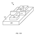
- FIG. 12A illustrates a non-planar multigate device including a split charge storage region
- FIG. 12B illustrates a cross-sectional view of the non-planar multigate device of FIG. 12A ;
- FIGS. 13A and 13B illustrate a non-planar multigate device including a split charge storage region and a horizontal nanowire channel
- FIG. 13C illustrates a cross-sectional view of a vertical string of non-planar multigate devices of FIG. 13A ;
- FIGS. 14A and 14B illustrate a non-planar multigate device including a split charge storage region and a vertical nanowire channel
- FIG. 15A through 15F illustrate a gate last scheme for fabricating the non-planar multigate device of FIG. 14A .
- the present invention includes a dielectric layer which is formed using a high density plasma oxidation process.
- the dielectric layer can be formed at a much lower temperature than competing deposition processes, such as chemical vapor deposition (CVD), in-situ steam oxidation (ISSG), and rapid thermal oxidation.
- CVD chemical vapor deposition
- ISSG in-situ steam oxidation
- the lower temperature provides the benefit of a reduced thermal budget and prevents the distortion of certain components which are sensitive to high temperatures, and prevents the diffusion of dopants from critical parts of devices.
- the high density plasma oxidation process results in a dielectric layer having a top surface which is much more uniform and smooth than that formed with competing deposition processes.
- the thickness of a layer beneath the dielectric layer can be reduced during the formation of the dielectric layer to a final thickness which is less than 20 ⁇ .
- semiconductor structures such as memory cells, can be formed with greater accuracy at smaller sizes.
- the invention provides a semiconductor device which has a higher reliability and a reduced manufacturing cost due to the lower thermal budget.
- a storage layer 130 is formed on a first dielectric layer 120 , which in turn is formed on a semiconductor substrate 100 .
- the semiconductor substrate 100 comprises a single crystal or polycrystalline silicon substrate, however, the semiconductor substrate 100 may comprise other materials. Suitable materials for semiconductor substrate 100 include silicon, gallium arsenide, germanium, gallium nitride, aluminum phosphide, Sil-xGex and AlxGal-xAs alloys, wherein x is greater than or equal to zero and less than or equal to one, the like, and combinations thereof. Additional examples of materials for semiconductor substrate 100 in accordance with the present invention are set forth in Semiconductor Device Fundamentals by Robert F. Pierret (p.
- the substrate 100 is loaded into a HDP system to form a dielectric layer 140 on the storage layer 130 in an oxygen and/or hydrogen ambient.
- source and drain regions 110 and 112 may be formed in the semiconductor substrate 100 by methods well known to those of ordinary skill in the art.
- the storage layer 130 may comprise SiN, as in a SONOS type device. In one embodiment, the storage layer 130 is a floating gate.
- the dielectric layer 120 may comprise silicon nitride, silicon oxynitride, or other oxides, nitrides, or oxynitrides.
- the first dielectric layer 120 is formed using a high density plasma (HDP) oxidation process similar to one used to form a second dielectric layer 140 , as discussed below.
- the dielectric layer 120 forms a tunneling oxide layer comprising SiO 2 , SiO 2 /Si 3 N 4 , or Si/SiO 2 .
- a second dielectric layer 140 is formed on the storage layer 130 using a high density plasma (HDP) oxidation process.
- This same HDP oxidation process can also be used to form the first dielectric layer 120 .
- this same HDP oxidation process can also be used to form any dielectric layer described herein.
- this same HDP oxidation process can be used to thin any silicon or nitride layer described herein by oxidizing a portion of the silicon or nitride layer described herein using HDP oxidation and removing said oxidized portion.
- the HDP oxidation process can also be used to form control oxide layers consisting of an oxide layer on a nitride layer on an oxide layer (an ONO structure).
- the second dielectric layer 140 comprises oxide, and more preferably, silicon oxide.
- the HDP oxidation process is conducted at a temperature preferably of less than 700° C., and more preferably less than 400° C. using high density plasma 170 . But the temperature can be easily controlled up to 700° C. by adjusting a bias 188 to the substrate 100 .
- the source of oxygen for the high density plasma 170 may be an oxygen containing precursor, or ambient 190 , such as O 2 , N 2 O, NO, CO, CO 2 , H 2 O or their mixture with any other inert gas (He, Ar, N, etc.), or an oxidizing gas (NO, N 2 O, O 2 , etc.).
- the high density plasma 170 is also formed using a hydrogen containing precursor, or ambient 190 , such as H 2 , NH 3 , D 2 , ND 3 .
- the high density plasma 170 may be generated by any one of a number of sources or HDP generating devices 176 , such as HDP CVD tools manufactured by Novellus Systems Inc. of San Jose, Calif. or Applied Materials of Santa Clara, Calif.
- sources or HDP generating devices 176 such as HDP CVD tools manufactured by Novellus Systems Inc. of San Jose, Calif. or Applied Materials of Santa Clara, Calif.
- one of the following sources may be used: helicon; helical-resonator; electron-cyclotron resonance; or inductively coupled plasma generator.
- the HDP generating device 176 is an HDP CVD tool in the SPEED line of tools manufactured by Novellus Systems Inc., of San Jose, Calif.
- the HDP generating device 176 includes a housing 177 having walls 178 surrounding and defining a chamber 171 .
- a coil 180 surrounds the housing 177 and is used to generate an electromagnetic field.
- Low frequency power is applied to the coil 180 at first through a bias 186 .
- Secondary power may be applied to a wafer holder 182 through the bias 188 to control the temperature of the substrate 100 .
- the housing 177 forms an opening 184 through which a passageway 172 is formed.
- the opening 184 allows for an ambient 190 to be introduced into the chamber 171 .
- the ambient 190 is later converted into high density plasma 170 in the chamber 171 .
- the semiconductor substrate 100 rests on a wafer holder 182 within the chamber 171 , on which high density plasma 170 is deposited using an HDP oxidation process.
- the substrate 100 can be unbiased, in which case ionized substances are accelerated by the plasma potential (on the order of 20 Volts) and then implanted into or onto the substrate 100 .
- a bias can be applied to the substrate 100 to further accelerate the ions from the high density plasma and deposit them or implant them deeper into the surface of the substrate 100 . Either a DC or RF bias may be applied to the substrate 100 .
- the following process conditions are used by the HDP generating device 176 to create an HDP oxidation process used to form the second dielectric layer 140 .
- the HDP generating device 176 is placed in an unbiased and unclamped (UBUC) mode.
- UBUC unbiased and unclamped
- a certain amount of low frequency power is applied to the first power node 186 and a certain amount of high frequency power is applied to the second power node 188 .
- high frequency power is applied to the first power node 186 and low frequency power is applied to the second power node 188 .
- the first power node 186 is connected with the coil 180 and the second power node 188 is connected with the wafer holder 182 .
- the low frequency power applied has a wattage from 1000 W to 30000 W, and more preferably from 2000 W to 25000 W, and more preferably about 3000 W.
- the low frequency power is applied having a frequency from 100 kHz to 1000 kHz, and more preferably a frequency from 200 kHz to 600 kHz, and even more preferably a frequency of 300 kHz to 500 kHz, and even more preferably about 450 kHz. ⁇ 10%, and most preferably greater than 400 kHz and less than 2000 kHz.
- High frequency power may also be applied to the coil 180 .
- no high frequency power is applied, and more preferably high frequency power is applied having a wattage from 0 W to 50 W, and a frequency of between 12 and 14 MHz, and most preferably about 13.56 MHz.
- Ambient 190 is introduced into the chamber 171 , preferably having a mixture of oxygen and hydrogen.
- the oxygen is O2 having a flow rate from 10 standard cubic centimeters per minute (sccm) to 1000 sccm, and more preferably from 90 sccm to 500 sccm, and most preferably from 100 sccm to 400 sccm.
- the hydrogen is H 2 having a flow rate from 10 sccm to 1000 sccm, and more preferably from 90 sccm to 500 sccm, and most preferably from 100 sccm to 400 sccm.
- the flow rate of the O 2 is within ⁇ 10% of the flow rate of the H 2 , and more preferably the flow rate of the O2 is within ⁇ 5% of the flow rate of the H 2 , and most preferably the flow rate of the O 2 is about the same as the flow rate of the H 2 .
- the thickness t 0 of the second dielectric layer 140 has good uniformity.
- the temperature of the semiconductor substrate 100 on the wafer holder 182 is set in the UBUC mode to a temperature which is preferably less than 700° C., and more preferably less than 400° C., and even more preferably from 300° C. to 400° C., and even more preferably from 325° C. to 375° C., and most preferably about 350° C. ⁇ 10%.
- the temperature of the semiconductor substrate 100 can later be controlled by application of bias power (i.e. ion bombardment).
- bias power i.e. ion bombardment
- the amount of time required to run the HDP oxidation process can vary depending on the amount of dielectric material desired for making the second dielectric layer 140 .
- the HDP oxidation process is run from 10 to 120 seconds, and more preferably from 20 to 60 seconds, and more preferably about 30 seconds ⁇ 10%.
- a portion of the layer on which the dielectric layer is formed on is oxidized.
- the dielectric layer, and the oxidized portion of the layer on which the dielectric layer is formed on are both removed.
- the second dielectric layer 140 is formed on a storage layer 130 which comprises Si 3 N 4 or SiO 2 , and the thickness of the storage layer 130 is reduced through oxidization of a portion of the storage layer 130 .
- the second dielectric layer 140 and the oxide formed on the storage layer 130 are then removed by applying an etch, such as a hydrofluoric acid (HF) solution, to the second dielectric layer 140 , reducing the thickness of the storage layer 130 .
- an etch such as a hydrofluoric acid (HF) solution
- the thickness of the storage layer 130 is measured upon removal of the oxidized portion, and a third dielectric layer (not shown) is formed on the storage layer 130 after the second dielectric layer 140 is removed.
- the first dielectric layer 120 is formed on the semiconductor substrate 100 using the high density plasma (HDP) oxidation process discussed herein.
- the HDP oxidation process is conducted at a temperature preferably of less than 700° C. using high density plasma 170 .
- the source of oxygen for the high density plasma 170 may be an oxygen containing precursor, or ambient 190 , such as of O 2 , H 2 , or their mixture with any other inert gas (He, Ar, N, etc.), or an oxidizing gas (NO, N 2 O, O 2 , etc.).
- the high density plasma 170 may be generated by any one of a number of sources or HDP generating devices 176 .
- the first dielectric layer 120 can be formed with a lower thermal budget than by conventional means.
- the semiconductor structure 116 shown in FIG. 1 is formed by patterning the first dielectric layer 120 , the storage layer 130 , and the second dielectric layer 140 to form a tunneling structure 122 from the first dielectric layer 120 , a storage node 132 from the storage layer 130 , and a blocking structure 142 from the second dielectric layer 140 .
- a gate electrode 152 is formed on the blocking structure 142 and first and second sidewall spacers 160 and 162 are formed on each side of the stack of the tunneling structure 122 , the storage node 132 , the blocking structure 142 , and the gate electrode 152 , as shown in FIG. 1 .
- first and second doped regions 110 and 112 can be formed in the substrate 100 .
- the semiconductor structure 116 can then be placed in a semiconductor device.
- the storage node 132 can be a floating gate, or can be part of a SONOS device.
- FIGS. 5 and 6 depict charts regarding SiO2 formation on Si and on a Si3N4 substrate.
- FIG. 5 depicts a first set of profiles which chart the oxide thickness in angstroms of either SiO 2 formed on Si 3 N 4 or SiO 2 formed on Si in relation to the flow rate of H 2 in sccm.
- FIG. 5 depicts a second set of profiles which chart the thickness uniformity in percent of either SiO 2 formed on Si 3 N 4 or SiO 2 formed on Si in relation to the flow rate of H 2 in sccm.
- FIG. 5 depicts a first set of profiles which chart the oxide thickness in angstroms of either SiO 2 formed on Si 3 N 4 or SiO 2 formed on Si in relation to the flow rate of H 2 in sccm.
- the HDP generating device 176 used the following process conditions: a low frequency wattage of 3000 W, a time of 60 seconds, a flow rate of 100 sccm for an O 2 ambient, and a flow rate of 300 sccm for a He ambient.
- a low frequency wattage of 3000 W a low frequency wattage of 3000 W
- a time of 60 seconds a flow rate of 100 sccm for an O 2 ambient
- a flow rate of 300 sccm for a He ambient As shown in FIG. 5 , the best thickness uniformity for the dielectric layer which is formed during the process shown in FIG. 5 occurs when the flow rate of the O 2 ambient equals the flow rate of an H 2 ambient.
- FIG. 6 depicts a second set of profiles which chart the thickness uniformity in percent of either SiO 2 formed on Si 3 N 4 or SiO 2 formed on Si in relation to the flow rate of O 2 in sccm.
- the HDP generating device 176 used the following process conditions: a low frequency wattage of 3000 W, a time of 60 seconds, a flow rate of 400 sccm for an H 2 ambient, and a flow rate of 300 sccm for an He ambient.
- the best thickness uniformity for the dielectric layer which is formed during the process shown in FIG. 6 occurs when the flow rate of the O 2 ambient equals the flow rate of an H 2 ambient.
- Table A shown below, indicates the Rms, the Ra, and the Rmax, all in angstroms ( ⁇ ), for the surface roughness of a dielectric layer formed using the above described HDP oxidation process, using an in-situ steam oxidation (ISSG) process, using an HTO process, and using an HTO+(GOX100) process.
- Table A illustrates how the Rms, the Ra, and the Rmax, are all lowest when using the above described HDP oxidation process.
- the HDP oxidation process forms a second dielectric layer 140 with a surface roughness having a Rms of less than 2.70 ⁇ , and more preferably of less than 2.50 ⁇ and most preferably of less than 2.20 ⁇ .
- the HDP oxidation process forms a second dielectric layer 140 with a surface roughness having a Ra of less than 2.15 ⁇ and more preferably of less than 2.0 ⁇ , and most preferably of less than 1.75 ⁇ .
- the HDP oxidation process forms a second dielectric layer 140 with a surface roughness having a Rmax of less than 26 ⁇ , and more preferably of less than 20 ⁇ and most preferably of less than 19 ⁇ .
- the storage layer 130 whose thickness is reduced when using the HDP oxidation process, can also be formed with much more uniformity and therefore lower Rms, Ra, and Rmax values than comparable processes. As a result, the final thickness (t f ) of the storage layer 130 can also be greatly reduced with respect to competing deposition processes.
- FIG. 7 depicts a chart which compares the differences between nitrogen and oxygen accumulation in atomic percentage at varying depths in a layer, such as the storage layer 130 , when using either a high density plasma oxidation process or an in-situ steam oxidation process.
- a layer such as the storage layer 130
- FIG. 7 depicts a chart which compares the differences between nitrogen and oxygen accumulation in atomic percentage at varying depths in a layer, such as the storage layer 130 , when using either a high density plasma oxidation process or an in-situ steam oxidation process.
- FIG. 8 depicts a flowchart illustration of oxide formation on a dielectric using a high density plasma oxidation process.
- a determination is made as to what type of structure is to be formed, either an ONO structure having a second dielectric layer 140 on a storage layer 130 comprising nitride on a first dielectric layer 120 , or an OSO structure in which the storage layer 130 comprises silicon.
- a second dielectric layer 140 is formed on the storage layer 130 using the above described HDP oxidation process.
- the HDP oxidation process also thins the storage layer 130 .
- oxide from the second dielectric layer 140 is removed, preferably using a hydrofluoric acid solution.
- the thickness of the storage layer 130 is measured. If the thickness is sufficient, then the process moves to 340 ; if the thickness is insufficient, then the process moves back to 310 .
- a final dielectric layer is formed on the storage layer 130 to form a quantumized stacked layer having either an ONO structure or an OSO structure.
- each of the layers of either the ONO structure or the OSO structure is less than 50 ⁇ thick and more preferably less than 20 ⁇ thick.
- a charge-storage node may be formed with multiple charge storage layers including multiple nitride layers having differing concentrations of oxygen, nitrogen and/or silicon.
- the nitride layers may include at least a first or bottom nitride layer overlying the tunneling layer and a second or top nitride layer overlying the bottom nitride layer.
- At least the bottom nitride layer may comprise silicon oxynitride (e.g. SixOyNx).
- the stoichiometric compositions of the layers may be tailored or selected such that the lower or bottom nitride is oxygen-rich, having a high oxygen to produce an oxygen-rich nitride or oxynitride.
- the top nitride layer is silicon-rich, nitrogen-rich and oxygen-lean, having a high silicon and a high nitrogen concentration with a low oxygen concentration to produce a silicon-rich nitride or oxynitride.
- the oxygen-rich bottom nitride layer results in it being a substantially trap free layer, thereby reducing the stored charge loss of charges stored in the top nitride layer without compromising device speed or an initial (beginning of life) difference between program and erase voltages.
- the silicon-rich, oxygen-lean top nitride layer results in it being a trap dense layer, thereby increasing a difference between programming and erase voltages when the structure is employed in memory devices, improving device speed, increasing data retention, and extending the operating life of the device.
- the silicon-rich, oxygen-lean top oxynitride layer can further include a concentration of carbon of from about 5% to about 9% to increase the number of traps therein.
- the multi-layer charge-storage node structure may further include a middle oxide or anti-tunneling layer between the two nitride layers, forming a split charge storage region comprising two nitride layers separated by a relatively thin oxide layer to further increase charge retention.
- FIG. 9 is a block diagram illustrating a cross-sectional side view of one such memory transistor or device 900 .
- the memory device 900 includes a silicon-oxide-nitride-oxide-nitride-silicon (SONONOS) stack 902 including an ONONO structure 904 formed over a surface 906 of a substrate 908 .
- Substrate 908 includes one or more diffusion regions 910 , such as source and drain regions, aligned to the gate stack 902 and separated by a channel region 912 .
- the SONONOS stack 902 includes a polysilicon or metal gate 914 formed upon and in contact with the ONONO structure 904 .
- the gate 914 is separated or electrically isolated from the substrate 908 by the ONONO structure 904 .
- the ONONO structure 904 includes a thin, lower oxide layer or tunneling layer 916 that separates or electrically isolates a multi-layer charge-storage node 918 a - c from the channel region 912 , and a blocking oxide layer or blocking structure 920 formed by HDP oxidation as described above.
- the multi-layer charge-storage node 918 a - c includes multiple nitride containing charge storage layers, including a bottom nitride layer 918 a , and a top oxynitride layer 918 b .
- the multi-layer charge-storage node 918 a - c further includes an intermediate oxide layer or anti-tunneling layer 918 c .
- the memory device 900 further includes first and second dielectric sidewall spacers 922 formed on each side of the stack of the SONONOS stack 902 , as shown in FIG. 9 .
- the various layers of the device 900 may be fabricated to certain thicknesses. Different possibilities for the thicknesses are described herein, representing possible different embodiments.
- the middle oxide layer will be relatively thin in comparison to the two nitride layers.
- the middle oxide may be between approximately 5 ⁇ and 20 ⁇ .
- the nitride layers may be the same or different thicknesses as one another, but will typically be at least approximately 30 ⁇ . With advances in process technology and material science, nitride thicknesses as low as 20 ⁇ may be possible in the near future.
- FIGS. 10A, 10B and 11 A method of fabricating the memory device 900 of FIG. 9 will now be described with reference to FIGS. 10A, 10B and 11 .
- the process begins with forming a tunneling layer 1002 over a channel 1004 connecting a source 1006 and a drain 1008 formed in a surface of a substrate 1012 (step 1102 ).
- the tunneling layer 1002 can be formed or deposited by any suitable means, including a plasma oxidation process, In-Situ Steam Generation (ISSG) or a radical oxidation process.
- the tunneling layer 1002 is formed in a HDP oxidation performed in an HDP generating device to effect growth of the tunneling layer by oxidation consumption of a portion of the substrate 1012 .
- the first or bottom nitride or nitride containing layer 1014 a of the multi-layer charge-storage node is formed on a surface of the tunneling layer 1002 (step 1104 ).
- the bottom nitride layer 1014 a can include silicon nitride or silicon oxynitride.
- the bottom nitride layer 1014 a is formed or deposited in a low pressure CVD process using a silicon source, such as silane (SiH 4 ), chlorosilane (SiH 3 Cl), dichlorosilane or DCS (SiH 2 Cl 2 ), tetrachlorosilane (SiCl 4 ) or Bis-TertiaryButylAmino Silane (BTBAS), a nitrogen source, such as nitrogen (N 2 ), ammonia (NH 3 ), nitrogen trioxide (NO 3 ) or nitrous oxide (N 2 O), and an oxygen-containing gas, such as oxygen (O 2 ) or N 2 O.
- a silicon source such as silane (SiH 4 ), chlorosilane (SiH 3 Cl), dichlorosilane or DCS (SiH 2 Cl 2 ), tetrachlorosilane (SiCl 4 ) or Bis-TertiaryButylAmino Silane (BT
- gases in which hydrogen has been replaced by deuterium can be used, including, for example, the substitution of deuterated-ammonia (ND 3 ) for NH 3 .
- the substitution of deuterium for hydrogen advantageously passivates Si dangling bonds at the silicon-oxide interface, thereby improving the endurance and retention performance of the SONOS device.
- the lower or bottom nitride layer 1014 a can be deposited over the tunneling layer 1002 by placing the substrate 1012 in a deposition chamber and introducing a process gas including N 2 O, NH 3 and DCS, while maintaining the chamber at a pressure of from about 5 milliTorr (mT) to about 500 mT, and maintaining the substrate at a temperature of from about 700 degrees Celsius to about 850° C. and in certain embodiments at least about 760° C. for a period of from about 2.5 minutes to about 20 minutes.
- a process gas including N 2 O, NH 3 and DCS
- the process gas can include a first gas mixture of N 2 O and NH 3 mixed in a ratio of from about 8:1 to about 1:8 and a second gas mixture of DCS and NH 3 mixed in a ratio of from about 1:7 to about 7:1, and can be introduced at a flow rate of from about 5 to about 200 standard cubic centimeters per minute (sccm). It has been found that a nitride or oxynitride layer produced or deposited under these condition yields an oxygen-rich, bottom nitride layer 1014 a.
- an anti-tunneling layer 1014 c is formed or deposited on a surface of the bottom nitride layer 1014 a (step 1106 ).
- the anti-tunneling layer 1014 c can be formed or deposited by any suitable means, including a plasma oxidation process, In-Situ Steam Generation (ISSG) or a radical oxidation process.
- the radical oxidation process involves flowing hydrogen (H 2 ) and oxygen (O 2 ) gas into a batch-processing chamber or furnace to effect growth of the anti-tunneling layer by oxidation consumption of a portion of the bottom nitride layer 1014 a.
- the second or top nitride layer 1014 b of the multi-layer charge storage layer is then formed on a surface of the anti-tunneling layer 1014 c (step 1108 ) to an initial thickness (t i ) of from about 30 to about 130 ⁇ .
- the top nitride layer 1014 b can be deposited over the anti-tunneling layer 1014 c in a CVD process using a process gas including N 2 O, NH 3 and DCS, at a chamber pressure of from about 5 mT to about 500 mT, and at a substrate temperature of from about 700° C. to about 850° C. and in certain embodiments at least about 760° C., for a period of from about 2.5 minutes to about 20 minutes.
- the process gas can include a first gas mixture of N 2 O and NH 3 mixed in a ratio of from about 8:1 to about 1:8 and a second gas mixture of DCS and NH 3 mixed in a ratio of from about 1:7 to about 7:1, and can be introduced at a flow rate of from about 5 to about 20 sccm.
- an oxynitride layer produced or deposited under these condition yields a silicon-rich, nitrogen-rich, and oxygen-lean top nitride layer 1014 b , which improves the speed and increases of the initial difference between program and erase voltage without compromising a charge loss rate of memory devices made using an embodiment of the silicon-oxide-oxynitride-oxide-silicon structure, thereby extending the operating life of the device.
- the silicon-rich, nitrogen-rich, and oxygen-lean top nitride layer can be deposited over the anti-tunneling layer in a CVD process using a process gas including BTBAS and ammonia (NH 3 ) mixed at a ratio of from about 7:1 to about 1:7 to further include a concentration of carbon selected to increase the number of traps therein.
- the selected concentration of carbon in the second oxynitride layer can include a carbon concentration of from about 5% to about 15%.
- Either or both of the oxygen-rich first or bottom nitride layer 1014 a and the oxygen-lean second or top nitride layer 1014 b can be formed in a single wafer tool or in a batch furnce using a CVD process.
- a first dielectric layer 1016 of an HDP oxide blocking structure is formed on a surface of the second layer 1014 b of the multi-layer charge storage layer using the above described HDP oxidation process.
- the HDP oxidation process begins with forming the first dielectric layer 1016 while thinning the second layer 1014 b of the multi-layer charge storage layer (step 1110 ).
- the high density plasma may be generated by any one of a number of sources or HDP generating devices, such as described above with respect to FIG. 4 .
- the process conditions used by the HDP generating device to create an HDP oxidation process used to form the first dielectric layer 1016 substantially the same as those described above with respect to FIGS. 2-8 .
- the HDP oxidation process is conducted using an oxygen containing precursor, or ambient, such as O 2 , N 2 O, NO, CO, CO 2 , H 2 O or their mixture with any other inert gas (He, Ar, N, etc.), or an oxidizing gas (NO, N 2 O, O 2 , etc.), and, optionally, a hydrogen containing precursor, or ambient, such as H 2 , NH 3 , D 2 , ND 3 .
- an oxygen containing precursor, or ambient such as O 2 , N 2 O, NO, CO, CO 2 , H 2 O or their mixture with any other inert gas (He, Ar, N, etc.), or an oxidizing gas (NO, N 2 O, O 2 , etc.)
- a hydrogen containing precursor, or ambient such as H 2 , NH 3 , D 2 , ND 3 .
- the HDP generating device is placed in an unbiased and unclamped (UBUC) mode, and a low frequency power of from 2000 W to 25000 W at 300 kHz to 500 kHz is applied to the first power node and a high frequency power of from 0 W to 50 W at 12 and 14 MHz, is applied to the second power node connected with the wafer holder.
- a mixture of oxygen having a flow rate from 100 sccm to 400 sccm and hydrogen having a flow rate from 100 sccm to 400 sccm is introduced into the chamber.
- the flow rate of the O 2 is within ⁇ 10% of the flow rate of the H 2 .
- the oxide thickness (t o ) of the first dielectric layer 1016 has good uniformity.
- the temperature of the substrate 100 on the wafer holder 182 is set in the UBUC mode to a temperature from 325° C. to 375° C.
- a high density plasma 1018 is then created which begins an HDP oxidation process which is used to form the first dielectric layer 1016 .
- the amount of time required to run the HDP oxidation process can vary depending on the amount of dielectric material desired for making the first dielectric layer 1016 . In one embodiment, the HDP oxidation process is run from 10 to 120 seconds, and more preferably from 20 to 60 seconds, and more preferably about 30 seconds ⁇ 10%.
- the final thickness (t f ) of the second layer 1014 b of the multi-layer charge storage layer is measured (step 1114 ). If a measured thickness is less than a predetermined thickness, i.e., less than about 30 to about 70 ⁇ , then the process moves back to step 1110 . If the thickness is sufficient, a second or final dielectric layer is formed on the first dielectric layer of the HDP oxide blocking structure to form a quantumized stacked layer having either an ONNO structure or an ONONO structure (step 1116 ).
- the final thickness of the top nitride can be from about 20 to about 35 ⁇ and the thickness of the blocking layer can be from about 20 to about 40 may be at least 30 ⁇ .
- multigate or multigate-surface memory devices including charge storage regions overlying two or more sides of a channel formed on or above a surface of a substrate, and methods of fabricating the same.
- Multigate devices include both planar and non-planar devices.
- a planar multigate device generally includes a double-gate planar device in which a number of first layers are deposited to form a first gate below a subsequently formed channel, and a number of second layers are deposited thereover to form a second gate.
- a non-planar multigate device generally includes a horizontal or vertical channel formed on or above a surface of a substrate and surrounded on three or more sides by a gate.
- FIGS. 12A and 12B illustrate an embodiment of one such semiconductor memory device 1200 .
- the memory device 1200 includes a channel region 1202 formed from a thin film or layer of semiconducting material overlying a surface 1204 on a substrate 1206 connecting a source region 1208 and a drain region 1210 of the memory transistor.
- the channel region 1202 is enclosed on three sides by a fin which forms a gate 1212 of the device.
- the thickness of the gate 1212 determines the effective channel region length of the device.
- the channel region 1202 can comprise polysilicon or recrystallized polysilicon to form a monocrystalline channel region.
- the channel region 1202 can be formed to have ⁇ 100> surface crystalline orientation relative to a long axis of the channel region.
- the non-planar multigate memory device 1200 of FIG. 12A can include a multi-layer charge storage region.
- FIG. 12B is a cross-sectional view of a portion of the non-planar memory transistor of FIG. 12A including a portion of the substrate 1206 , channel region 1202 and the gate 1212 illustrating a gate electrode 1214 and a multi-layer charge storage region 1216 .
- the gate 1212 further includes a tunneling layer 1218 overlying a raised channel region 1202 , and an HDP oxide blocking structure 1220 overlying the multi-layer charge storage region 1216 to form a control gate of the memory device 1200 .
- the channel region 1202 and gate 1212 can be formed directly on substrate 1206 or on an insulating or dielectric layer 1222 , such as a buried oxide layer, formed on or over the substrate.
- the HDP oxide blocking structure 1220 includes at least first dielectric layer formed on a surface of the second layer 1216 b of the multi-layer charge storage layer 1216 using the above described HDP sources or generating devices and process conditions.
- the gate electrode 1214 can include a doped polysilicon layer formed or deposited in a low pressure CVD process and can have a thickness of from about 200 ⁇ to about 2000 ⁇ .
- the multi-layer charge storage region 1216 includes at least one lower or bottom oxygen-rich first nitride layer 1216 a including nitride closer to the tunneling layer 1218 , and an upper or top oxygen-lean second nitride layer 1216 b overlying the oxygen-rich first nitride layer.
- the oxygen-lean second nitride layer 1216 b includes a silicon-rich, oxygen-lean nitride layer and includes a majority of a charge traps distributed in the multi-layer charge storage region, while the oxygen-rich first nitride layer 1216 a includes an oxygen-rich nitride or silicon oxynitride, and is oxygen-rich relative to the oxygen-lean second nitride layer to reduce the number of charge traps therein.
- oxygen-rich it is meant wherein a concentration of oxygen in the oxygen-rich first nitride layer 1216 a is from about 15 to about 40%, whereas a concentration of oxygen in oxygen-lean second nitride layer 1216 b is less than about 5%.
- the multi-layer charge storage region 1216 further includes at least one thin, intermediate or anti-tunneling layer 1216 c including a dielectric, such as an oxide, separating the oxygen-lean second nitride layer 1216 b from the oxygen-rich first nitride layer 1216 a .
- the anti-tunneling layer 1216 c substantially reduces the probability of electron charge that accumulates at the boundaries of the oxygen-lean second nitride layer 1216 b during programming from tunneling into the first nitride layer 1216 a.
- either or both of the oxygen-rich first nitride layer 1216 a and the oxygen-lean second nitride layer 1216 b can include silicon nitride or silicon oxynitride, and can be formed, for example, by a CVD process including N 2 O/NH 3 and DCS/NH 3 gas mixtures in ratios and at flow rates tailored to provide a silicon-rich and oxygen-rich oxynitride layer.
- the second nitride layer of the multi-layer charge storage structure is then formed on the middle oxide layer.
- the oxygen-lean second nitride layer 1216 b has a stoichiometric composition of oxygen, nitrogen and/or silicon different from that of the oxygen-rich first nitride layer 1216 a , and may also be formed or deposited by a CVD process using a process gas including DCS/NH 3 and N 2 O/NH 3 gas mixtures in ratios and at flow rates tailored to provide a silicon-rich, oxygen-lean top nitride layer. Either or both of the oxygen-rich first nitride layer 1216 a and the oxygen-lean second nitride layer 1216 b can be formed in a single wafer tool or in a batch furnce using a CVD process.
- the anti-tunneling layer can be formed by oxidation of the bottom oxynitride layer, to a chosen depth using radical oxidation.
- Radical oxidation may be performed, for example, at a temperature of 1000-1100 degrees Celsius using a single wafer tool, or 800-900 degrees Celsius using a batch reactor tool.
- a mixture of H 2 and O 2 gasses may be employed at a pressure of 300-500 Torr for a batch process, or 10-15 Torr using a single vapor tool, for a time of 1-2 minutes using a single wafer tool, or 30 min-1 hour using a batch process.
- a suitable thickness for the oxygen-rich first nitride layer 1216 a may be from about 30 ⁇ to about 160 ⁇ (with some variance permitted, for example ⁇ 10 A), of which about 5-20 ⁇ may be consumed by radical oxidation to form the anti-tunneling layer 1216 c .
- a suitable thickness for the oxygen-lean second nitride layer 1216 b may be at least 30 ⁇ .
- the oxygen-lean second nitride layer 1216 b may be formed up to 130 ⁇ thick, of which 30-70 ⁇ may be consumed by HDP oxidation to form the HDP oxide blocking structure 1220 .
- a ratio of thicknesses between the oxygen-rich first nitride layer 1216 a and oxygen-lean second nitride layer 1216 b is approximately 1:1 in some embodiments, although other ratios are also possible.
- the HDP oxide blocking structure 1220 may further include a second or final dielectric layer.
- the final dielectric layer may be a high K dielectric layer.
- Suitable high K dielectrics include hafnium based materials such as HfSiON, HfSiO or HfO, Zirconium based material such as ZrSiON, ZrSiO or ZrO, and Yttrium based material such as Y 2 O 3 .
- the memory transistor can include a nanowire channel region formed from a thin film of semiconducting material overlying a surface on a substrate connecting a source region and a drain region of the memory transistor.
- nanowire channel region it is meant a conducting channel region formed in a thin strip of semiconducting material.
- the nanowire is a silicon nanowire with a conducting channel region formed in a thin strip of crystalline silicon material, having a maximum cross-sectional dimension of about 10 nanometers (nm) or less, and more preferably less than about 6 nm.
- the memory device or transistor 1300 includes a horizontal nanowire channel region 1302 formed from a thin film or layer of semiconducting material on or overlying a surface on a substrate 1306 , and connecting a source region 1308 and a drain region 1310 of the memory transistor.
- the device has a gate-all-around (GAA) structure in which the nanowire channel region 1302 is enclosed on all sides by a gate 1312 of the device.
- the thickness of the gate 1312 determines the effective channel region length of the device.
- the nanowire channel region 1302 can comprise polysilicon or recrystallized polysilicon to form a monocrystalline channel region.
- the channel region 1302 can be formed to have ⁇ 100> surface crystalline orientation relative to a long axis of the channel region.
- the non-planar multigate memory transistor 1300 of FIG. 13A can include a multi-layer charge storage region and an HDP oxide blocking structure formed at least in part by oxidation of a top layer of the multi-layer charge storage region.
- FIG. 13B is a cross-sectional view of a portion of the non-planar memory transistor of FIG. 13A including a portion of the substrate 1306 , nanowire channel region 1302 and the gate 1312 .
- the gate 1312 includes a tunneling layer 1318 overlying the nanowire channel region 1302 , a multi-layer charge storage region 1316 a - 1316 c , an HDP oxide blocking structure 1320 , and a gate electrode 1314 .
- the HDP oxide blocking structure 1320 includes at least first dielectric layer formed on a surface of the second layer 1316 b of the multi-layer charge storage layer 1316 using the above described HDP sources or generating devices and process conditions.
- the gate electrode 1314 includes a doped polysilicon layer formed or deposited in a low pressure CVD process and having a thickness of from about 200 ⁇ to about 2000 ⁇ .
- the polysilicon layer of the gate electrode 1314 can be formed or grown directly as a doped polysilicon layer through the addition of gases such as phosphine, arsine, diborane or BF 2 .
- the multi-layer charge storage region 1316 a - 13716 c includes at least one inner oxygen-rich first nitride layer 1316 a comprising nitride closer to the tunneling layer 1318 , and an outer oxygen-lean second nitride layer 1316 b overlying the oxygen-rich first nitride layer.
- the outer oxygen-lean second nitride layer 1316 b comprises a silicon-rich, oxygen-lean nitride layer and comprises a majority of a charge traps distributed in the multi-layer charge storage region
- the oxygen-rich first nitride layer 1316 a comprises an oxygen-rich nitride or silicon oxynitride, and is oxygen-rich relative to the outer oxygen-lean second nitride layer to reduce the number of charge traps therein.
- the multi-layer charge storage region 1316 further includes at least one thin, intermediate or anti-tunneling layer 1316 c comprising a dielectric, such as an oxide, separating outer oxygen-lean second nitride layer 1316 b from the oxygen-rich first nitride layer 1316 a .
- the anti-tunneling layer 1316 c substantially reduces the probability of electron charge that accumulates at the boundaries of outer oxygen-lean second nitride layer 1316 b during programming from tunneling into the oxygen-rich first nitride layer 1316 a , resulting in lower leakage current.
- either or both of the oxygen-rich first nitride layer 1316 a and the outer oxygen-lean second nitride layer 1316 b can comprise silicon nitride or silicon oxynitride, and can be formed, for example, by a CVD process including N 2 O/NH 3 and DC S/NH 3 gas mixtures in ratios and at flow rates tailored to provide a silicon-rich and oxygen-rich oxynitride layer.
- the second nitride layer of the multi-layer charge storage structure is then formed on the middle oxide layer.
- the outer oxygen-lean second nitride layer 1316 b has a stoichiometric composition of oxygen, nitrogen and/or silicon different from that of the oxygen-rich first nitride layer 1316 a , and may also be formed or deposited by a CVD process using a process gas including DCS/NH 3 and N 2 O/NH 3 gas mixtures in ratios and at flow rates tailored to provide a silicon-rich, oxygen-lean top nitride layer.
- the anti-tunneling layer can be formed by oxidation of the oxygen-rich first nitride layer 1316 a , to a chosen depth using radical oxidation.
- Radical oxidation may be performed, for example, at a temperature of 1000-1100 degrees Celsius using a single wafer tool, or 800-900 degrees Celsius using a batch reactor tool.
- a mixture of H 2 and O 2 gasses may be employed at a pressure of 300-500 Torr for a batch process, or 10-15 Torr using a single vapor tool, for a time of 1-2 minutes using a single wafer tool, or 30 min-1 hour using a batch process.
- a suitable thickness for the oxygen-rich first nitride layer 1316 a may be from about 30 ⁇ to about 80 ⁇ (with some variance permitted, for example ⁇ 10 A), of which about 5-20 ⁇ may be consumed by radical oxidation to form the anti-tunneling layer 1316 c .
- a suitable thickness for the outer oxygen-lean second nitride layer 1316 b may be at least 30 ⁇ .
- the outer oxygen-lean second nitride layer 1316 b may be formed up to 70 ⁇ thick, of which 30-70 ⁇ may be consumed by HDP oxidation to form the HDP oxide blocking structure 1320 .
- a ratio of thicknesses between the oxygen-rich first nitride layer 1316 a and the outer oxygen-lean second nitride layer 1316 b is approximately 1:1 in some embodiments, although other ratios are also possible.
- the HDP oxide blocking structure 1320 may further include a second or final dielectric layer.
- the final dielectric layer may be a high K dielectric layer.
- Suitable high K dielectrics include hafnium based materials such as HfSiON, HfSiO or HfO, Zirconium based material such as ZrSiON, ZrSiO or ZrO, and Yttrium based material such as Y 2 O 3 .
- FIG. 13C illustrates a cross-sectional view of a vertical string of non-planar multigate transistors 1300 of FIG. 13A arranged in a Bit-Cost Scalable or BiCS architecture 1326 .
- the BiCS architecture 1326 consists of a vertical string or stack of non-planar multigate transistors 1300 , where each device or cell includes a nanowire channel region 1302 overlying the substrate 1306 , and connecting a source region and a drain region (not shown in this figure) of the memory transistor, and having a gate-all-around (GAA) structure in which the nanowire channel region 1302 is enclosed on all sides by a gate 1312 .
- GAA gate-all-around
- the BiCS architecture reduces number of critical lithography steps compared to a simple stacking of layers, leading to a reduced cost per memory bit.
- the memory transistor is or includes a non-planar device comprising a vertical nanowire channel region formed in or from a semiconducting material projecting above or from a number of conducting, semiconducting layers on a substrate.
- the memory transistor 1400 comprises a vertical nanowire channel region 1402 formed in a cylinder of semiconducting material connecting a source region 1404 and drain region 1406 of the device.
- the channel region 1402 is surrounded by a tunneling layer 1408 , a multi-layer charge storage region 1410 , a HDP oxide blocking structure 1412 and an electrode 1414 overlying the HDP oxide blocking structure to form a control gate of the memory transistor 1400 .
- the channel region 1402 can include an annular region in an outer layer of a substantially solid cylinder of semiconducting material, or can include an annular layer formed over a cylinder of dielectric filler material.
- the channel region 1402 can comprise polysilicon or recrystallized polysilicon to form a monocrystalline channel region.
- the channel region 1402 can be formed to have ⁇ 100> surface crystalline orientation relative to a long axis of the channel region.
- the multi-layer charge storage region 1410 includes at least an inner or oxygen-rich first nitride layer 1410 a closest to the tunneling layer 1408 , and an outer or oxygen-lean second nitride layer 1410 b .
- the oxygen-rich first nitride layer 1410 a and the oxygen-lean second nitride layer 1410 b are separated by an intermediate oxide or anti-tunneling layer 1410 c comprising oxide.
- Either or both of the oxygen-rich first nitride layer 1410 a and the oxygen-lean second nitride layer 1410 b can comprise silicon nitride or silicon oxynitride, and can be formed, for example, by a CVD process including N 2 O/NH 3 and DCS/NH 3 gas mixtures in ratios and at flow rates tailored to provide a silicon-rich and oxygen-rich oxynitride layer.
- the HDP oxide blocking structure 1412 includes at least first dielectric layer formed on a surface of the second layer 1410 b of the multi-layer charge storage layer 1410 using the above described HDP sources or generating devices and process conditions.
- either or both of the oxygen-lean second nitride layer 1410 b and the HDP oxide blocking structure 1412 may comprise a high K dielectric, such as HfSiON, HfSiO, HfO, ZrSiON, ZrSiO, ZrO, or Y 2 O 3 .
- the memory transistor 1400 of FIG. 14A can be made using a gate last scheme.
- a dielectric layer 1502 such as an oxide, is formed over a sacrificial layer 1504 on a surface on a substrate 1506 , an opening etched through the dielectric and sacrificial layers and a vertical channel region 1508 formed therein.
- the vertical channel region 1508 can include an annular region in an outer layer of a substantially solid cylinder of semiconducting material 1510 , such as polycrystalline or monocrystalline silicon, or can include a separate, layer semiconducting material surrounding a cylinder of dielectric filler material (not shown).
- the dielectric layer 1502 can comprise any suitable dielectric material, such as a silicon oxide, capable of electrically isolating the subsequently formed gate electrode of the memory transistor 800 from an overlying electrically active layer or another memory transistor.
- a second opening 1512 is etched through the etched through the dielectric layer 1502 and sacrificial layer 1504 to the substrate 1506 , and the sacrificial layer 1504 at least partially etched or removed.
- the sacrificial layer 1504 can comprise any suitable material that can be etched or removed with high selectivity relative to the material of the dielectric layer 1502 , substrate 1506 and vertical channel region 1508 .
- the sacrificial layer 1504 comprises an oxide that can be removed by Buffered Oxide Etch (BOE etch).
- a tunneling layer 1514 , a multi-layer charge storage region 1516 A-C, and an HDP oxide blocking structure 1518 are sequentially deposited in the opening, and the surface of the dielectric layer 1502 planarized to yield the intermediate structure shown in FIG. 15C .
- HDP oxide blocking structure 1518 includes at least first dielectric layer formed on a surface of the second layer 1516 b of the multi-layer charge storage layer 1516 using the above described HDP sources or generating devices and process conditions.
- the multi-layer charge storage layer 1516 A-C is a split multi-layer charge storage layer including at least an inner oxygen-rich first nitride layer 1516 A closest to the tunneling layer 1514 , and an outer, oxygen-lean second nitride layer 1516 B.
- the first and second charge storage layers can be separated by an intermediate oxide or anti-tunneling layer 1516 c.
- a gate electrode layer 1522 is deposited into the second opening 1512 and the surface of the upper dielectric layer 1502 planarized to yield the intermediate structure illustrated in FIG. 15E .
- the gate electrode layer 1522 includes a doped polysilicon layer having a dopant concentration of from about 1e14 cm ⁇ 2 to about 1e16 cm ⁇ 2 so that the minimum energy needed to remove an electron from the gate electrode is from at least about 4.8 eV to about 5.3 eV.
- the polysilicon layer of the gate electrode layer 1522 is grown directly as a doped polysilicon layer through the addition of gases such as phosphine, arsine, diborane or BF 2 , to the CVD process.
- an opening 1524 is etched through the gate electrode layer 1522 to form control gates of separate memory devices 1526 A and 1526 B.
Abstract
Description
| TABLE A | |||||
| HDP | ON | ON with | |||
| OXIDIZED | with | HTO + | |||
| ON | HTO | (GOX100) | |||
| Rms (Å) | 2.15 | 3.02 | 2.91 | ||
| (−26%) | (+4%) | (0%) | |||
| Ra (Å) | 1.70 | 2.39 | 2.29 | ||
| (−26%) | (+4%) | (0%) | |||
| Rmax (Å) | 18.18 | 26.86 | 29.41 | ||
| (−38%) | (−9%) | (0%) | |||
Claims (14)
Priority Applications (4)
| Application Number | Priority Date | Filing Date | Title |
|---|---|---|---|
| US14/969,468 US9460974B1 (en) | 2007-08-09 | 2015-12-15 | Oxide formation in a plasma process |
| US15/266,239 US10128258B2 (en) | 2007-08-09 | 2016-09-15 | Oxide formation in a plasma process |
| US16/135,897 US10319733B2 (en) | 2007-08-09 | 2018-09-19 | Oxide formation in a plasma process |
| US16/434,856 US20200161324A1 (en) | 2007-08-09 | 2019-06-07 | Oxide formation in a plasma process |
Applications Claiming Priority (5)
| Application Number | Priority Date | Filing Date | Title |
|---|---|---|---|
| US11/836,683 US8119538B1 (en) | 2007-08-09 | 2007-08-09 | Oxide formation in a plasma process |
| US13/401,712 US8822349B1 (en) | 2007-08-09 | 2012-02-21 | Oxide formation in a plasma process |
| US201414473634A | 2014-08-29 | 2014-08-29 | |
| US14/562,462 US9406574B1 (en) | 2007-08-09 | 2014-12-05 | Oxide formation in a plasma process |
| US14/969,468 US9460974B1 (en) | 2007-08-09 | 2015-12-15 | Oxide formation in a plasma process |
Related Parent Applications (1)
| Application Number | Title | Priority Date | Filing Date |
|---|---|---|---|
| US14/562,462 Continuation US9406574B1 (en) | 2007-08-09 | 2014-12-05 | Oxide formation in a plasma process |
Related Child Applications (1)
| Application Number | Title | Priority Date | Filing Date |
|---|---|---|---|
| US15/266,239 Continuation US10128258B2 (en) | 2007-08-09 | 2016-09-15 | Oxide formation in a plasma process |
Publications (1)
| Publication Number | Publication Date |
|---|---|
| US9460974B1 true US9460974B1 (en) | 2016-10-04 |
Family
ID=56507299
Family Applications (5)
| Application Number | Title | Priority Date | Filing Date |
|---|---|---|---|
| US14/562,462 Active US9406574B1 (en) | 2007-08-09 | 2014-12-05 | Oxide formation in a plasma process |
| US14/969,468 Active US9460974B1 (en) | 2007-08-09 | 2015-12-15 | Oxide formation in a plasma process |
| US15/266,239 Active US10128258B2 (en) | 2007-08-09 | 2016-09-15 | Oxide formation in a plasma process |
| US16/135,897 Active US10319733B2 (en) | 2007-08-09 | 2018-09-19 | Oxide formation in a plasma process |
| US16/434,856 Abandoned US20200161324A1 (en) | 2007-08-09 | 2019-06-07 | Oxide formation in a plasma process |
Family Applications Before (1)
| Application Number | Title | Priority Date | Filing Date |
|---|---|---|---|
| US14/562,462 Active US9406574B1 (en) | 2007-08-09 | 2014-12-05 | Oxide formation in a plasma process |
Family Applications After (3)
| Application Number | Title | Priority Date | Filing Date |
|---|---|---|---|
| US15/266,239 Active US10128258B2 (en) | 2007-08-09 | 2016-09-15 | Oxide formation in a plasma process |
| US16/135,897 Active US10319733B2 (en) | 2007-08-09 | 2018-09-19 | Oxide formation in a plasma process |
| US16/434,856 Abandoned US20200161324A1 (en) | 2007-08-09 | 2019-06-07 | Oxide formation in a plasma process |
Country Status (1)
| Country | Link |
|---|---|
| US (5) | US9406574B1 (en) |
Cited By (3)
| Publication number | Priority date | Publication date | Assignee | Title |
|---|---|---|---|---|
| US20170005108A1 (en) * | 2007-08-09 | 2017-01-05 | Cypress Semiconductor Corporation | Oxide formation in a plasma process |
| US10332810B2 (en) | 2016-10-24 | 2019-06-25 | Kla-Tencor Corp. | Process modules integrated into a metrology and/or inspection tool |
| WO2021180099A1 (en) * | 2020-03-10 | 2021-09-16 | 长鑫存储技术有限公司 | Method for testing stability of x-ray photoelectron spectrometer |
Families Citing this family (6)
| Publication number | Priority date | Publication date | Assignee | Title |
|---|---|---|---|---|
| KR102293874B1 (en) * | 2014-12-10 | 2021-08-25 | 삼성전자주식회사 | Semiconductor devices and methods of manufacturing thereof |
| US10026745B1 (en) * | 2017-01-13 | 2018-07-17 | United Microelectronics Corp. | Semiconductor memory cell structure |
| CN107219448B (en) * | 2017-06-07 | 2019-03-26 | 西安电子科技大学 | The barrier layer internal trap of constant is distributed characterizing method when based on feature |
| CN107703430B (en) * | 2017-09-11 | 2019-02-22 | 西安电子科技大学 | The measurement method that surface state trap influences device output characteristics |
| CN107703431B (en) * | 2017-09-11 | 2019-02-22 | 西安电子科技大学 | Device surface state trap measurement method based on changeable frequency pulse technique |
| US11569390B2 (en) * | 2019-12-23 | 2023-01-31 | Micron Technology, Inc. | Memory cells and integrated assemblies having charge-trapping-material with trap-enhancing-additive |
Citations (19)
| Publication number | Priority date | Publication date | Assignee | Title |
|---|---|---|---|---|
| US5434109A (en) * | 1993-04-27 | 1995-07-18 | International Business Machines Corporation | Oxidation of silicon nitride in semiconductor devices |
| US6271112B1 (en) * | 1998-11-13 | 2001-08-07 | Advanced Micro Devices, Inc. | Interlayer between titanium nitride and high density plasma oxide |
| US20020004277A1 (en) * | 2000-02-28 | 2002-01-10 | Micron Technology, Inc. | Structure and method for dual gate oxide thicknesses |
| US20020013114A1 (en) * | 1998-08-07 | 2002-01-31 | Hisashi Ohtani | Semiconductor device and method of manufacturing the same |
| US6458650B1 (en) * | 2001-07-20 | 2002-10-01 | Taiwan Semiconductor Manufacturing Company | CU second electrode process with in situ ashing and oxidation process |
| US20030026158A1 (en) * | 2001-07-30 | 2003-02-06 | Matrix Semiconductor, Inc. | Anti-fuse memory cell with asymmetric breakdown voltage |
| US20050045942A1 (en) | 2003-08-10 | 2005-03-03 | Anam Semiconductor Inc. | Semiconductor device and fabricating method thereof |
| US20050260107A1 (en) * | 2003-07-01 | 2005-11-24 | Jackson David P | Method, process, chemistry and apparatus for treating a substrate |
| US20070249127A1 (en) * | 2006-04-24 | 2007-10-25 | Freescale Semiconductor, Inc. | Electronic device including a semiconductor layer and a sidewall spacer and a process of forming the same |
| US20080014718A1 (en) | 2006-07-13 | 2008-01-17 | S.O.I Tec Silicon On Insulator Technologies S.A. | Treatment for bonding interface stabilization |
| US20080224205A1 (en) * | 2004-03-15 | 2008-09-18 | Pooran Chandra Joshi | Vertical Thin-Film Transistor with Enhanced Gate Oxide |
| US20080237684A1 (en) * | 2007-03-26 | 2008-10-02 | Michael Specht | Method of manufacturing a nanowire transistor, a nanowire transistor structure, a nanowire transistor field |
| US20080251833A1 (en) * | 2007-04-12 | 2008-10-16 | Michael Specht | Integrated circuits and methods of manufacture |
| US20080296655A1 (en) * | 2007-05-31 | 2008-12-04 | United Microelectronics Corp. | Multi-time programmable memory and method of manufacturing the same |
| US20100065899A1 (en) * | 2008-09-16 | 2010-03-18 | Kim Suk-Pil | Semiconductor devices including auxiliary gate electrodes and methods of fabricating the same |
| US20110204332A1 (en) * | 2010-02-25 | 2011-08-25 | Samsung Electronics Co., Ltd. | Semiconductor device and method of manufacturing the same |
| US20110280076A1 (en) * | 2010-05-17 | 2011-11-17 | Sandisk Corporation | Junctionless tft nand flash memory |
| US8119538B1 (en) | 2007-08-09 | 2012-02-21 | Cypress Semiconductor Corporation | Oxide formation in a plasma process |
| US9018693B2 (en) * | 2007-07-20 | 2015-04-28 | Cypress Semiconductor Corporation | Deuterated film encapsulation of nonvolatile charge trap memory device |
Family Cites Families (8)
| Publication number | Priority date | Publication date | Assignee | Title |
|---|---|---|---|---|
| US8592891B1 (en) * | 2007-05-25 | 2013-11-26 | Cypress Semiconductor Corp. | Methods for fabricating semiconductor memory with process induced strain |
| US8643124B2 (en) * | 2007-05-25 | 2014-02-04 | Cypress Semiconductor Corporation | Oxide-nitride-oxide stack having multiple oxynitride layers |
| US8691648B1 (en) * | 2007-05-25 | 2014-04-08 | Cypress Semiconductor Corporation | Methods for fabricating semiconductor memory with process induced strain |
| US9449831B2 (en) * | 2007-05-25 | 2016-09-20 | Cypress Semiconductor Corporation | Oxide-nitride-oxide stack having multiple oxynitride layers |
| US8940645B2 (en) * | 2007-05-25 | 2015-01-27 | Cypress Semiconductor Corporation | Radical oxidation process for fabricating a nonvolatile charge trap memory device |
| US20090179253A1 (en) * | 2007-05-25 | 2009-07-16 | Cypress Semiconductor Corporation | Oxide-nitride-oxide stack having multiple oxynitride layers |
| US9406574B1 (en) | 2007-08-09 | 2016-08-02 | Cypress Semiconductor Corporation | Oxide formation in a plasma process |
| US7799670B2 (en) * | 2008-03-31 | 2010-09-21 | Cypress Semiconductor Corporation | Plasma oxidation of a memory layer to form a blocking layer in non-volatile charge trap memory devices |
-
2014
- 2014-12-05 US US14/562,462 patent/US9406574B1/en active Active
-
2015
- 2015-12-15 US US14/969,468 patent/US9460974B1/en active Active
-
2016
- 2016-09-15 US US15/266,239 patent/US10128258B2/en active Active
-
2018
- 2018-09-19 US US16/135,897 patent/US10319733B2/en active Active
-
2019
- 2019-06-07 US US16/434,856 patent/US20200161324A1/en not_active Abandoned
Patent Citations (21)
| Publication number | Priority date | Publication date | Assignee | Title |
|---|---|---|---|---|
| US5434109A (en) * | 1993-04-27 | 1995-07-18 | International Business Machines Corporation | Oxidation of silicon nitride in semiconductor devices |
| US20020013114A1 (en) * | 1998-08-07 | 2002-01-31 | Hisashi Ohtani | Semiconductor device and method of manufacturing the same |
| US6271112B1 (en) * | 1998-11-13 | 2001-08-07 | Advanced Micro Devices, Inc. | Interlayer between titanium nitride and high density plasma oxide |
| US20020004277A1 (en) * | 2000-02-28 | 2002-01-10 | Micron Technology, Inc. | Structure and method for dual gate oxide thicknesses |
| US6458650B1 (en) * | 2001-07-20 | 2002-10-01 | Taiwan Semiconductor Manufacturing Company | CU second electrode process with in situ ashing and oxidation process |
| US20030026158A1 (en) * | 2001-07-30 | 2003-02-06 | Matrix Semiconductor, Inc. | Anti-fuse memory cell with asymmetric breakdown voltage |
| US20050260107A1 (en) * | 2003-07-01 | 2005-11-24 | Jackson David P | Method, process, chemistry and apparatus for treating a substrate |
| US20050045942A1 (en) | 2003-08-10 | 2005-03-03 | Anam Semiconductor Inc. | Semiconductor device and fabricating method thereof |
| US20080224205A1 (en) * | 2004-03-15 | 2008-09-18 | Pooran Chandra Joshi | Vertical Thin-Film Transistor with Enhanced Gate Oxide |
| US20070249127A1 (en) * | 2006-04-24 | 2007-10-25 | Freescale Semiconductor, Inc. | Electronic device including a semiconductor layer and a sidewall spacer and a process of forming the same |
| US20080014718A1 (en) | 2006-07-13 | 2008-01-17 | S.O.I Tec Silicon On Insulator Technologies S.A. | Treatment for bonding interface stabilization |
| US20080237684A1 (en) * | 2007-03-26 | 2008-10-02 | Michael Specht | Method of manufacturing a nanowire transistor, a nanowire transistor structure, a nanowire transistor field |
| US20080251833A1 (en) * | 2007-04-12 | 2008-10-16 | Michael Specht | Integrated circuits and methods of manufacture |
| US20080296655A1 (en) * | 2007-05-31 | 2008-12-04 | United Microelectronics Corp. | Multi-time programmable memory and method of manufacturing the same |
| US7763928B2 (en) * | 2007-05-31 | 2010-07-27 | United Microelectronics Corp. | Multi-time programmable memory |
| US9018693B2 (en) * | 2007-07-20 | 2015-04-28 | Cypress Semiconductor Corporation | Deuterated film encapsulation of nonvolatile charge trap memory device |
| US8119538B1 (en) | 2007-08-09 | 2012-02-21 | Cypress Semiconductor Corporation | Oxide formation in a plasma process |
| US20100065899A1 (en) * | 2008-09-16 | 2010-03-18 | Kim Suk-Pil | Semiconductor devices including auxiliary gate electrodes and methods of fabricating the same |
| US20110204332A1 (en) * | 2010-02-25 | 2011-08-25 | Samsung Electronics Co., Ltd. | Semiconductor device and method of manufacturing the same |
| US8823077B2 (en) * | 2010-02-25 | 2014-09-02 | Samsung Electronics Co., Ltd. | Semiconductor device and method of manufacturing the same |
| US20110280076A1 (en) * | 2010-05-17 | 2011-11-17 | Sandisk Corporation | Junctionless tft nand flash memory |
Non-Patent Citations (12)
| Title |
|---|
| USPTO Advisory Action for U.S. Appl. No. 13/401,712 dated Jan. 24, 2014; 3 pages. |
| USPTO Advisory Action for U.S. Appl. No. 13/401,712 dated Jun. 7, 2013; 3 pages. |
| USPTO Final Rejection for U.S. Appl. No. 11/836,683 dated Feb. 4, 2010; 13 pages. |
| USPTO Final Rejection for U.S. Appl. No. 13/401,712 dated Apr. 3, 2013; 17 pages. |
| USPTO Final Rejection for U.S. Appl. No. 13/401,712 dated Nov. 6, 2013; 13 pages. |
| USPTO Non-Final Rejection for U.S. Appl. No. 11/836,683 dated Aug. 8, 2011; 17 pages. |
| USPTO Non-Final Rejection for U.S. Appl. No. 11/836,683 dated Jul. 7, 2009; 15 pages. |
| USPTO Non-Final Rejection for U.S. Appl. No. 13/401,712 dated Jul. 15, 2013; 5 pages. |
| USPTO Non-Final Rejection for U.S. Appl. No. 13/401,712 dated Nov. 23, 2012; 15 pages. |
| USPTO Notice of Allowance for U.S. Appl. No. 11/836,683 dated Dec. 23, 2011; 9 pages. |
| USPTO Notice of Allowance for U.S. Appl. No. 13/401,712 dated Feb. 28, 2014; 7 pages. |
| USPTO Notice of Allowance for U.S. Appl. No. 14/562,462 dated Aug. 26, 2015; 13 pages. |
Cited By (6)
| Publication number | Priority date | Publication date | Assignee | Title |
|---|---|---|---|---|
| US20170005108A1 (en) * | 2007-08-09 | 2017-01-05 | Cypress Semiconductor Corporation | Oxide formation in a plasma process |
| US10128258B2 (en) * | 2007-08-09 | 2018-11-13 | Cypress Semiconductor Corporation | Oxide formation in a plasma process |
| US10319733B2 (en) | 2007-08-09 | 2019-06-11 | Cypress Semiconductor Corporation | Oxide formation in a plasma process |
| US10332810B2 (en) | 2016-10-24 | 2019-06-25 | Kla-Tencor Corp. | Process modules integrated into a metrology and/or inspection tool |
| WO2021180099A1 (en) * | 2020-03-10 | 2021-09-16 | 长鑫存储技术有限公司 | Method for testing stability of x-ray photoelectron spectrometer |
| US11327033B1 (en) | 2020-03-10 | 2022-05-10 | Changxin Memory Technologies, Inc. | Methods for detecting stability of X-ray photoelectron spectrometer |
Also Published As
| Publication number | Publication date |
|---|---|
| US20170005108A1 (en) | 2017-01-05 |
| US9406574B1 (en) | 2016-08-02 |
| US10128258B2 (en) | 2018-11-13 |
| US20200161324A1 (en) | 2020-05-21 |
| US20190088669A1 (en) | 2019-03-21 |
| US10319733B2 (en) | 2019-06-11 |
Similar Documents
| Publication | Publication Date | Title |
|---|---|---|
| US10319733B2 (en) | Oxide formation in a plasma process | |
| US11456365B2 (en) | Memory transistor with multiple charge storing layers and a high work function gate electrode | |
| US11784243B2 (en) | Oxide-nitride-oxide stack having multiple oxynitride layers | |
| US20230074163A1 (en) | Sonos ono stack scaling | |
| US8063434B1 (en) | Memory transistor with multiple charge storing layers and a high work function gate electrode | |
| US8710578B2 (en) | SONOS stack with split nitride memory layer | |
| CN111180525B (en) | Oxide nitride oxide stack with multiple oxynitride layers | |
| WO2014008166A1 (en) | Memory transistor with multiple charge storing layers | |
| TW201347048A (en) | Integration of non-volatile charge trap memory devices and logic CMOS devices | |
| JP2004193414A (en) | Nonvolatile semiconductor memory and its manufacturing method |
Legal Events
| Date | Code | Title | Description |
|---|---|---|---|
| AS | Assignment |
Owner name: MORGAN STANLEY SENIOR FUNDING, INC., NEW YORK Free format text: SECURITY INTEREST;ASSIGNOR:CYPRESS SEMICONDUCTOR CORPORATION;REEL/FRAME:039676/0237 Effective date: 20160805 |
|
| STCF | Information on status: patent grant |
Free format text: PATENTED CASE |
|
| AS | Assignment |
Owner name: CYPRESS SEMICONDUCTOR CORPORATION, CALIFORNIA Free format text: ASSIGNMENT OF ASSIGNORS INTEREST;ASSIGNORS:BYUN, JEONG SOO;RAMKUMAR, KRISHNASWAMY;REEL/FRAME:043719/0489 Effective date: 20070809 |
|
| AS | Assignment |
Owner name: MORGAN STANLEY SENIOR FUNDING, NEW YORK Free format text: CORRECTIVE ASSIGNMENT TO CORRECT THE FOLLOWING NUMBERS 6272046,7277824,7282374,7286384,7299106,7337032,7460920,7519447 PREVIOUSLY RECORDED ON REEL 039676 FRAME 0237. ASSIGNOR(S) HEREBY CONFIRMS THE SECURITY INTEREST;ASSIGNOR:CYPRESS SEMICONDUCTOR CORPORATION;REEL/FRAME:047797/0854 Effective date: 20171229 |
|
| AS | Assignment |
Owner name: LONGITUDE FLASH MEMORY SOLUTIONS LTD., IRELAND Free format text: ASSIGNMENT OF ASSIGNORS INTEREST;ASSIGNOR:CYPRESS SEMICONDUCTOR CORPORATION;REEL/FRAME:049086/0803 Effective date: 20190503 |
|
| AS | Assignment |
Owner name: SPANSION LLC, CALIFORNIA Free format text: RELEASE BY SECURED PARTY;ASSIGNOR:MORGAN STANLEY SENIOR FUNDING, INC.;REEL/FRAME:049109/0573 Effective date: 20190503 Owner name: CYPRESS SEMICONDUCTOR CORPORATION, CALIFORNIA Free format text: RELEASE BY SECURED PARTY;ASSIGNOR:MORGAN STANLEY SENIOR FUNDING, INC.;REEL/FRAME:049109/0573 Effective date: 20190503 |
|
| MAFP | Maintenance fee payment |
Free format text: PAYMENT OF MAINTENANCE FEE, 4TH YEAR, LARGE ENTITY (ORIGINAL EVENT CODE: M1551); ENTITY STATUS OF PATENT OWNER: LARGE ENTITY Year of fee payment: 4 |
|
| MAFP | Maintenance fee payment |
Free format text: PAYMENT OF MAINTENANCE FEE, 8TH YEAR, LARGE ENTITY (ORIGINAL EVENT CODE: M1552); ENTITY STATUS OF PATENT OWNER: LARGE ENTITY Year of fee payment: 8 |