US9406496B2 - Method and system for improving characteristic peak signals in analytical electron microscopy - Google Patents
Method and system for improving characteristic peak signals in analytical electron microscopy Download PDFInfo
- Publication number
- US9406496B2 US9406496B2 US13/681,245 US201213681245A US9406496B2 US 9406496 B2 US9406496 B2 US 9406496B2 US 201213681245 A US201213681245 A US 201213681245A US 9406496 B2 US9406496 B2 US 9406496B2
- Authority
- US
- United States
- Prior art keywords
- scanning protocol
- beam scanning
- incident beam
- incident
- electron
- Prior art date
- Legal status (The legal status is an assumption and is not a legal conclusion. Google has not performed a legal analysis and makes no representation as to the accuracy of the status listed.)
- Active
Links
- 238000000034 method Methods 0.000 title claims abstract description 37
- 238000001493 electron microscopy Methods 0.000 title description 3
- 239000002178 crystalline material Substances 0.000 claims abstract description 10
- 238000013507 mapping Methods 0.000 claims abstract description 7
- 238000010894 electron beam technology Methods 0.000 claims description 19
- 230000005540 biological transmission Effects 0.000 claims description 12
- 229920005994 diacetyl cellulose Polymers 0.000 claims description 10
- 230000033001 locomotion Effects 0.000 claims description 8
- 230000036962 time dependent Effects 0.000 claims description 8
- 230000006698 induction Effects 0.000 claims description 7
- 230000004075 alteration Effects 0.000 claims description 6
- 230000000295 complement effect Effects 0.000 claims description 6
- 230000008569 process Effects 0.000 claims description 5
- 238000012545 processing Methods 0.000 claims description 3
- 229920006395 saturated elastomer Polymers 0.000 claims 3
- 238000005430 electron energy loss spectroscopy Methods 0.000 abstract description 40
- 238000004611 spectroscopical analysis Methods 0.000 abstract description 15
- 238000005259 measurement Methods 0.000 abstract description 13
- 238000002149 energy-dispersive X-ray emission spectroscopy Methods 0.000 abstract description 4
- 239000000523 sample Substances 0.000 description 46
- 241000252073 Anguilliformes Species 0.000 description 37
- 238000001228 spectrum Methods 0.000 description 13
- 230000001965 increasing effect Effects 0.000 description 8
- 239000000463 material Substances 0.000 description 8
- 230000000694 effects Effects 0.000 description 7
- 238000002003 electron diffraction Methods 0.000 description 7
- 238000002474 experimental method Methods 0.000 description 6
- 230000008859 change Effects 0.000 description 5
- 239000013078 crystal Substances 0.000 description 5
- 238000000851 scanning transmission electron micrograph Methods 0.000 description 5
- 230000005465 channeling Effects 0.000 description 4
- 230000001419 dependent effect Effects 0.000 description 4
- 230000003287 optical effect Effects 0.000 description 4
- 238000001878 scanning electron micrograph Methods 0.000 description 4
- 238000012916 structural analysis Methods 0.000 description 4
- 238000004458 analytical method Methods 0.000 description 3
- 230000008901 benefit Effects 0.000 description 3
- 230000009977 dual effect Effects 0.000 description 3
- 238000000619 electron energy-loss spectrum Methods 0.000 description 3
- 230000004044 response Effects 0.000 description 3
- 239000000126 substance Substances 0.000 description 3
- 229910002370 SrTiO3 Inorganic materials 0.000 description 2
- 238000002441 X-ray diffraction Methods 0.000 description 2
- 238000003384 imaging method Methods 0.000 description 2
- 230000010354 integration Effects 0.000 description 2
- 230000003993 interaction Effects 0.000 description 2
- 230000004048 modification Effects 0.000 description 2
- 238000012986 modification Methods 0.000 description 2
- 229910021421 monocrystalline silicon Inorganic materials 0.000 description 2
- 230000000737 periodic effect Effects 0.000 description 2
- 238000003325 tomography Methods 0.000 description 2
- 241000976924 Inca Species 0.000 description 1
- 229910025794 LaB6 Inorganic materials 0.000 description 1
- 238000003917 TEM image Methods 0.000 description 1
- 238000004097 X-ray Buerger Methods 0.000 description 1
- 238000004125 X-ray microanalysis Methods 0.000 description 1
- 230000003466 anti-cipated effect Effects 0.000 description 1
- 238000013459 approach Methods 0.000 description 1
- 201000009310 astigmatism Diseases 0.000 description 1
- 230000015556 catabolic process Effects 0.000 description 1
- 229910052729 chemical element Inorganic materials 0.000 description 1
- 239000013626 chemical specie Substances 0.000 description 1
- 230000001427 coherent effect Effects 0.000 description 1
- 230000001010 compromised effect Effects 0.000 description 1
- 238000013480 data collection Methods 0.000 description 1
- 230000007423 decrease Effects 0.000 description 1
- 230000007547 defect Effects 0.000 description 1
- 238000006731 degradation reaction Methods 0.000 description 1
- 230000000593 degrading effect Effects 0.000 description 1
- 238000001514 detection method Methods 0.000 description 1
- 238000002050 diffraction method Methods 0.000 description 1
- 238000006073 displacement reaction Methods 0.000 description 1
- 238000002524 electron diffraction data Methods 0.000 description 1
- 238000000724 energy-dispersive X-ray spectrum Methods 0.000 description 1
- 230000001939 inductive effect Effects 0.000 description 1
- 238000010884 ion-beam technique Methods 0.000 description 1
- 238000004452 microanalysis Methods 0.000 description 1
- 238000000386 microscopy Methods 0.000 description 1
- 238000001383 neutron diffraction data Methods 0.000 description 1
- 238000010606 normalization Methods 0.000 description 1
- 230000003534 oscillatory effect Effects 0.000 description 1
- 238000005070 sampling Methods 0.000 description 1
- 238000009738 saturating Methods 0.000 description 1
- 238000004626 scanning electron microscopy Methods 0.000 description 1
- 238000001350 scanning transmission electron microscopy Methods 0.000 description 1
- 230000035945 sensitivity Effects 0.000 description 1
- 230000003595 spectral effect Effects 0.000 description 1
- 230000001360 synchronised effect Effects 0.000 description 1
- 230000009897 systematic effect Effects 0.000 description 1
- 230000007704 transition Effects 0.000 description 1
- 238000004627 transmission electron microscopy Methods 0.000 description 1
Images


Classifications
-
- H—ELECTRICITY
- H01—ELECTRIC ELEMENTS
- H01J—ELECTRIC DISCHARGE TUBES OR DISCHARGE LAMPS
- H01J49/00—Particle spectrometers or separator tubes
- H01J49/44—Energy spectrometers, e.g. alpha-, beta-spectrometers
-
- G—PHYSICS
- G01—MEASURING; TESTING
- G01N—INVESTIGATING OR ANALYSING MATERIALS BY DETERMINING THEIR CHEMICAL OR PHYSICAL PROPERTIES
- G01N23/00—Investigating or analysing materials by the use of wave or particle radiation, e.g. X-rays or neutrons, not covered by groups G01N3/00 – G01N17/00, G01N21/00 or G01N22/00
- G01N23/22—Investigating or analysing materials by the use of wave or particle radiation, e.g. X-rays or neutrons, not covered by groups G01N3/00 – G01N17/00, G01N21/00 or G01N22/00 by measuring secondary emission from the material
- G01N23/225—Investigating or analysing materials by the use of wave or particle radiation, e.g. X-rays or neutrons, not covered by groups G01N3/00 – G01N17/00, G01N21/00 or G01N22/00 by measuring secondary emission from the material using electron or ion
- G01N23/2251—Investigating or analysing materials by the use of wave or particle radiation, e.g. X-rays or neutrons, not covered by groups G01N3/00 – G01N17/00, G01N21/00 or G01N22/00 by measuring secondary emission from the material using electron or ion using incident electron beams, e.g. scanning electron microscopy [SEM]
-
- G—PHYSICS
- G01—MEASURING; TESTING
- G01N—INVESTIGATING OR ANALYSING MATERIALS BY DETERMINING THEIR CHEMICAL OR PHYSICAL PROPERTIES
- G01N2223/00—Investigating materials by wave or particle radiation
- G01N2223/05—Investigating materials by wave or particle radiation by diffraction, scatter or reflection
- G01N2223/051—Investigating materials by wave or particle radiation by diffraction, scatter or reflection correcting for scatter
-
- G—PHYSICS
- G01—MEASURING; TESTING
- G01N—INVESTIGATING OR ANALYSING MATERIALS BY DETERMINING THEIR CHEMICAL OR PHYSICAL PROPERTIES
- G01N2223/00—Investigating materials by wave or particle radiation
- G01N2223/40—Imaging
- G01N2223/402—Imaging mapping distribution of elements
-
- H—ELECTRICITY
- H01—ELECTRIC ELEMENTS
- H01J—ELECTRIC DISCHARGE TUBES OR DISCHARGE LAMPS
- H01J2237/00—Discharge tubes exposing object to beam, e.g. for analysis treatment, etching, imaging
- H01J2237/15—Means for deflecting or directing discharge
- H01J2237/1505—Rotating beam around optical axis
-
- H—ELECTRICITY
- H01—ELECTRIC ELEMENTS
- H01J—ELECTRIC DISCHARGE TUBES OR DISCHARGE LAMPS
- H01J2237/00—Discharge tubes exposing object to beam, e.g. for analysis treatment, etching, imaging
- H01J2237/15—Means for deflecting or directing discharge
- H01J2237/1506—Tilting or rocking beam around an axis substantially at an angle to optical axis
- H01J2237/1507—Tilting or rocking beam around an axis substantially at an angle to optical axis dynamically, e.g. to obtain same impinging angle on whole area
-
- H—ELECTRICITY
- H01—ELECTRIC ELEMENTS
- H01J—ELECTRIC DISCHARGE TUBES OR DISCHARGE LAMPS
- H01J2237/00—Discharge tubes exposing object to beam, e.g. for analysis treatment, etching, imaging
- H01J2237/26—Electron or ion microscopes
- H01J2237/28—Scanning microscopes
- H01J2237/2803—Scanning microscopes characterised by the imaging method
- H01J2237/2808—Cathodoluminescence
-
- H—ELECTRICITY
- H01—ELECTRIC ELEMENTS
- H01J—ELECTRIC DISCHARGE TUBES OR DISCHARGE LAMPS
- H01J37/00—Discharge tubes with provision for introducing objects or material to be exposed to the discharge, e.g. for the purpose of examination or processing thereof
- H01J37/26—Electron or ion microscopes; Electron or ion diffraction tubes
- H01J37/28—Electron or ion microscopes; Electron or ion diffraction tubes with scanning beams
Definitions
- the invention relates to the use in electron microscopy of electron energy loss and energy dispersive x-ray spectroscopy for determining the local chemical composition of materials. More specifically, it relates to quantitative measurements of characteristic peak signals obtained from samples containing crystalline regions and the generation of compositional maps from such samples.
- Electron energy loss spectroscopy (“EELS”) relies on measurements of the energy distribution of incident electrons transmitted through the microscope sample, while energy dispersive x-ray spectroscopy (“EDS”) relies on measurements of the energy distribution of x-rays emitted from regions of the sample exposed to the incident electron beam.
- EDS energy dispersive x-ray spectroscopy
- EELS is better suited to lighter elements—corresponding to characteristic energy losses up to about 3 keV—while EDS is better suited to heavier elements—corresponding to characteristic x-ray energies up to about 30 keV.
- TEM transmission electron microscopy
- STEM scanning transmission electron microscopy
- SEM scanning electron microscopy
- EELS and EDS quantitative chemical information is obtained by measuring the intensity of the characteristic peaks (also called “edges” in EELS, in recognition of their distinctive shape) associated with particular elements, which are often observed against a highly non-uniform background.
- the strength of signal associated with a given peak or peaks, and thus the accuracy and sensitivity of the measurement of the concentration of a given element, can be affected by a range of factors, including local sample composition and morphology, the spatial/energy profile and coherence of the incident beam, and the resolution and other characteristics of the X-ray or EELS detection system, that, taken together, can be extremely difficult to quantify.
- the incident beam is frequently aligned close to a high symmetry crystallographic direction (also referred to as a “zone axis”).
- a high symmetry crystallographic direction also referred to as a “zone axis”.
- This can be deliberate—for example, when obtaining atomic resolution images in TEM/STEM or seeking information about crystallographic defects, such as grain boundaries or interfaces—or can occur accidentally, particularly when investigating polycrystalline materials comprised of crystallites having a range of different orientations.
- the coherent scattering by the periodic potential of the crystal can strongly affect the peak intensities measured in EELS or EDS.
- channeling makes it more difficult to extract meaningful compositional information from crystalline samples. For example, a change of only one degree in the orientation of the incident electron beam can lead to changes of as much as 20% in the apparent relative composition of two elements, as measured by the strength of the characteristic x-ray signal.
- Elemental composition maps can be generated by performing quantitative EELS or EDS peak measurements at multiple sample locations, assuming the difficulties noted above, associated with spectrum acquisition from discrete locations, can be overcome.
- compositional maps further difficulties are associated with the need to move the beam between different locations while maintaining consistent data collection conditions over extended time periods. These difficulties include sample degradation and drift and changes in signal intensity arising from electron optical, mechanical and electronic instabilities.
- the changes in EELS or EDS peak intensities from crystalline samples associated with small changes in the angle of the incident beam are of particular concern for compositional mapping, since the relative angle of the incident beam can be affected as the beam is moved between locations by changes in electron optical conditions or sample morphology. Such changes in relative incident beam angle with location are almost inevitable in studies of polycrystalline materials, which, as noted above, generally contain a range of differently orientated crystallites.
- PED precession electron diffraction
- PED can be qualitatively understood as suppressing the “dynamical” redistribution of intensity between incident and multiple diffracted beams associated with high symmetry directions, thereby approaching the more easily modeled “quasi-kinematical” conditions.
- a full theoretical understanding of the factors that govern the transition from dynamical to quasi-kinematical conditions in PED remains elusive. See E. Mugnaioli et al., “Ab Initio” Structure Solution from Electron Diffraction Data Obtained by a Combination of Automated Electron Tomography and Precession Technique, 109 Ultramicroscopy 758-65 (2009); T. A. White et al., Is Precession Electron Diffraction Kinematical ? [Parts I and II], 110 Ultramicroscopy 763-770 (2010).
- the present invention alleviates many of the difficulties of quantitative EDS and EELS measurements of samples containing crystalline or polycrystalline regions by applying a beam scanning protocol to maximize signal strength and diminish spurious signal variations associated with changes in relative incident beam angle, thereby allowing improved compositional mapping of samples containing crystalline or polycrystalline regions by STEM, TEM and SEM.
- a method for obtaining spectroscopic data from a sample of crystalline material in an electron microscope comprising configuring an electron beam to impinge on a location of the sample comprising a region of crystalline material, applying an incident beam scanning protocol that maintains the beam impinging on substantially the same sample location while varying over time one or both of the incident beam inclination angle and azimuthal angle, and acquiring a set of spectroscopic data while the beam scanning protocol is being applied.
- the spectroscopic data set comprises energy-resolved x-ray data acquired from x-rays emitted from the crystalline region.
- the spectroscopic data set comprises energy loss data acquired from a beam exiting the sample in a transmission electron microscope, with a complementary beam scanning protocol being applied to the exit beam to substantially remove the time-dependent movements arising from the incident beam scanning protocol.
- compositional information is derived from the spectroscopic data set.
- the incident beam scanning protocol is associated with an inclination angle, and the incident beam scanning protocol comprises processing the incident beam at a substantially constant inclination angle.
- the incident electron beam without the beam scanning protocol applied is substantially parallel with a high symmetry crystallographic direction of the crystalline region.
- the method further includes identifying a characteristic feature within the spectroscopic data set, acquiring from the location a plurality of data sets comprising the characteristic feature by applying the beam scanning protocol at a range of inclination angles, quantifying the characteristic feature for each of the plurality of data sets; and identifying an optimum inclination angle associated with the characteristic feature.
- the optimum inclination angle is the minimum inclination angle for which the quantified characteristic feature obtains a maximum value.
- Embodiments are disclosed in which the electron microscope comprises a number of beam deflection control circuits and the beam scanning protocol is applied by delivering a number of beam scanning protocol signals to the number of beam deflection control circuits, with the beam scanning protocol signals further comprising one or more of a time-dependent induction compensation component, a distortion compensation component, a lens precession and a lens aberration component.
- Also disclosed is a method for generating a composition map comprising applying any of the above methods to a multiplicity of sample locations and mapping the quantitative compositional information from the multiplicity of sample locations and the relative location of the multiplicity of sample locations onto a compositional map.
- a system comprising an external beam control device configured to deliver beam scanning protocol signals to the beam deflection control circuits of the electron microscope, with the external beam control device comprising digital to analog converters (“DACs”), each DAC configured to deliver the beam scanning protocol signals to one of the beam deflection control circuits.
- DACs digital to analog converters
- a control computer is configured to drive the external beam control device and to acquire and process electron energy loss and x-ray data.
- the external beam control device is configured to receive and compare images received at different times from a microscope detector and apply drift compensation.
- FIG. 1 is a schematic of a TEM configured to practice an embodiment of the invention.
- FIG. 2 is a schematic of a SEM configured to practice an embodiment of the invention.
- FIG. 3A shows a Si L 2,3 peak without and with precession at a 0.48° angle.
- FIG. 3B shows a Si L 2,3 peak signal enhancement as a function of precession angle
- FIG. 4 shows Ti L 2,3 and O K signal enhancement as a function of precession angle
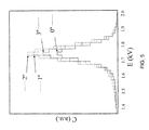
- FIG. 5 shows Si K-alpha signal without precession and with precession at angles of 1, 2 and 3°.
- a beam deflection control device is directed by a control computer and may be used to apply a beam scanning protocol during acquisition of EDS and/or EELS data to increase signal strength and reduce spurious signal variations.
- the control computer in other embodiment of the present invention are part of the original system installed in the microscope, or other embodiments is an external unit coupled to an external beam deflection control device.
- the control computer in certain embodiments of the present invention are configured to acquire and process images from SEM or STEM detectors (brightfield, darkfield, annular darkfield, backscatter, secondary electron, etc.), and acquire and process EDS and EELS data.
- a given beam scanning protocol may be optimized for characteristic EDS or EELS features corresponding to a given chemical element, allowing quantitative EDS or EELS data for one or more elements to be acquired in multiple locations of a sample for the generation of quantitative compositional maps.
- Different scanning protocols may be used in different embodiments of the invention. Precession of the type described by Vincent and Midgley may be used, in which the incident beam remains fixed on substantially the same location in the sample, is deflected by a fixed incident angle away from the unscanned direction (typically aligned with the optic axis of the electron microscope) and rotated rapidly around the azimuth at a uniform rotational speed.
- Other scanning protocols may involve the incident beam, again remaining fixed on substantially the same location of the sample, executing a series of pendulum-like movements that intersect, or pass close to, the unscanned incident beam direction (typically aligned on or close to the optic axis) and implementing a gradual rotation around the azimuth.
- the incident beam may be rotated at a variable rate or the azimuth may be changed by discrete amounts.
- Other scanning protocols may be employed, such as, for example, protocols involving directing the beam to conform to a series of discrete incident and azimuth coordinates, or to execute a series of scans between pairs of discrete incident and azimuth coordinates, again without deviating substantially from the location on the sample.
- the scanning protocol may have a time period with a frequency (or frequencies) adjusted to accommodate the acquisition time required for a particular characteristic peak or peaks.
- the chosen scanning protocol should have the net effect of imparting sufficient inclination to the incident beam to suppress dynamical scattering sufficiently to improve the strength of a characteristic EDS or EELS feature of interest while also not introducing systematic errors due to over sampling a particular azimuthal angle or set of angles.
- an incident angle associated with the scanning protocol should be amenable to identification and control.
- the required tilt angle may be set in the range of anywhere from about 0.1 to 2 degrees, possibly as high as 3 degrees, corresponding to the incident angle of the beam scanning protocol, applied with an azimuthal rotation in the range of 10-1000 Hz.
- precession angle and a precession frequency it should be understood that a variety of beam scanning protocols may be implemented in place of precession.
- One embodiment, shown in the schematic of FIG. 1 comprises a TEM, typically operating at an accelerating voltage in the range between 20 kV and 300 kV, coupled to an external beam deflection control device 112 .
- the TEM may further include an electron beam monochromator (not shown in the figure).
- the incident 103 and transmitted 105 beams may be steered using beam deflection control signals generated by the beam deflection control device 112 and delivered via connections, shown as dotted lines, running to the upper 101 and lower 102 beam deflection control circuits of the microscope.
- the position and/or angle of the incident beam 103 at the plane of the specimen 104 may be changed according to the signal level delivered by the beam control device 112 to the upper beam deflection control circuits 101 , typically connected to upper beam dual deflection coils shown as 101 A and 101 B, and the position and/or angle of the transmitted beam 105 entering the electron energy loss spectrometer 107 may be changed according to the signal level delivered at the lower beam deflection control circuits 102 , typically connected to upper beam dual deflection coils shown as 102 A and 102 B.
- the beam deflection control device may be aligned and configured to deliver complementary signals to the upper and lower beam deflection control circuits 101 and 102 , such that the position of EELS spectrum 108 on EELS detector 109 remains fixed as the incident beam angle and/or position at the sample is changed.
- the beam control device may be operated manually by the microscope operator, or may be driven by a control computer 113 , shown connected to the beam deflection control device 112 via dotted lines.
- the control computer 113 may also transmit instructions to, and acquire data from, EELS spectrometer 107 , EELS detector 109 , and EDS detector 110 , as shown by the dashed lines in the figure.
- the beam deflection control device 112 may also be connected to the STEM image detector 106 , as also shown by the dashed line in the figure, enabling it to acquire STEM images. (Though not shown in FIG. 1 , the STEM image detector 106 may also be connected to control computer 113 .)
- the TEM beam deflection control signals generated by beam control device may typically be delivered at rates between 0.1 Hz and 200 kHz.
- FIG. 2 Another embodiment shown in FIG. 2 comprises an SEM, typically with an accelerating voltage in the range between around 10 to 40 kV, coupled to a beam deflection control device 207 .
- the SEM may be combined with a focused ion beam (“FIB”) device.
- the beam deflection control device 207 may deliver beam deflection control signals to the microscope's beam deflection control circuits 201 , via a connection as shown by the dotted lines.
- the position and/or angle of the incident beam 202 at the plane of the specimen 204 may be changed according to the signal level (typically a voltage signal) delivered to the beam deflection control circuits 201 .
- the signal level typically a voltage signal
- the beam control device may be operated manually by the microscope operator, or may be driven according to instructions delivered by a control computer 208 , shown connected to the beam deflection control device 207 via dotted lines.
- the control computer 208 may also be connected to the EDS detector 203 , as shown by the dotted lines in the figure.
- the beam deflection control device 207 may also be connected to the SEM image detector 205 , in order to acquire SEM images, as illustrated by the dotted lines. (The control computer 208 may also be connected to secondary electron detector 205 , though this is not shown in FIG. 2 .)
- the SEM beam deflection control signals may typically be delivered by the beam deflection control device 207 at rates between 0.1 Hz and 200 kHz.
- Microscope beam deflection control circuits shown as 101 and 102 in the TEM configuration shown in FIG. 1, and 201 in the SEM configuration in FIG. 2 , generally accept a DC voltage signal, typically in the range of 5 to 20 V.
- the value of the DC voltage on each input of a beam deflection control circuit ( 101 , 102 , or 201 ) translates into the amount of deflection that circuit will induce in the electron beam.
- the deflection may typically be produced by pairs of dual-deflection beam coils, each pair comprising upper and lower beam coils, shown as upper coils 101 A and 102 A and lower coils 101 B and 102 B in the TEM configuration of FIG. 1 , and upper coils 201 A and lower coils 201 B in the SEM configuration of FIG.
- the beam deflection control device shown as 112 in FIG. 1 (and 207 in FIG. 2 , contains a series of digital-to analog converters (“DAC”s), one for each beam deflection coil to be addressed in the electron microscope.
- DAC digital-to analog converters
- a typical TEM system having eight such beam deflection coils, counting the orthogonally-disposed coils not shown in FIG. 1 therefore requires eight DACs in the beam deflection control device 112
- a typical SEM system having four beam deflection coils, counting the orthogonally-disposed coils not shown in FIG. 2 therefore requires four DACs in the beam deflection control device 208 .
- the sequence of voltage values delivered from the DACs to the microscope deflection control circuits may be programmed to deliver a range of different beam scanning protocol signals.
- the sequence of voltage values delivered from all eight DACs to a TEM may be synchronized at update rates of 192 kHz, in principle allowing the generation of virtually any form of beam scanning protocol incorporating beam displacement and/or beam tilt above or below the sample.
- the incident beam scanning protocol should not significantly increase the effective size of the incident beam on the sample by translating the area of the beam substantially beyond the sample location.
- the spectrum formed from the transmitted beam should also remain fixed and having the same entry angle for the detector, so it may be recorded without degrading energy resolution.
- synchronization between beam movement and precession may also be required. For example, if the rate at which the beam is moved between locations is not significantly different from the precession rate, synchronization between these rates may be needed to ensure that the beam is incident on each location and spectroscopic data acquired under the same conditions.
- Beam scanning protocol signals for example, delivered by the DACs noted above, may be distorted by the nonlinear response of the microscope beam deflection control circuits.
- an additional time-dependent nonlinear component (the “distortion compensation signal”) may be added to the beam scanning protocol signal.
- the deflection signal actually imparted to the electron beam may not match the shape of the beam scanning protocol signal delivered by the microscope deflection control circuits to the deflection coils.
- a time-dependent induction compensation component may be added to the beam scanning protocol signal.
- a complementary exit beam scanning protocol may be applied using a phase-shifted and appropriately scaled version of the incident beam scanning protocol. For example, for circular precession at a uniform speed of the incident beam, an appropriately scaled and phase-shifted sinusoidal signal may be applied to the lower beam deflection control circuits.
- additional adjustments to the amplitudes and phases may be required in order to compensate for the time-dependent motion of the exit beam arising from the incident beam scanning protocol, the non-linear behavior of the exit beam deflection circuits and frequency-dependent induction effects in the lower beam deflection coils, as discussed above, and for additional precession of the electron beam caused, in particular, by the magnetic field of the objective lens (referred to here as lens precession).
- Higher-order objective lens aberrations generally 3rd-order astigmatism
- each of the above-mentioned distortions in particular the non-linear behavior of microscope control circuits, may be amplitude- and frequency-dependent, it may be necessary to define a different distortion compensation signals for each combination of precession amplitude and frequency.
- a suitably large precession frequency may be selected such that, for each spectrum (or spectroscopic data set) acquired, the beam rotates a large number of cycles (typically more than 100).
- a smaller, but integral number of precession cycles may be used for the acquisition of each spectrum (or spectroscopic data set). For example, for a spectrum acquired using an integration time of 2 seconds, any frequency greater than about 50 Hz may be acceptable, whereas for an integration time of only 0.1 seconds, any lower frequency that is a multiple of 10 Hz may be applied.
- the beam deflection control device may be pre-aligned. This may be done by either selecting a stored set of pre-alignment values, or by adjusting each of the beam deflection control signals to its pre-aligned value.
- the pre-alignment may be performed at a large precession angle, typically approximately half the maximum feasible precession angle of the microscope system. (The feasible precession angle for a TEM may be significantly less than that available in an SEM.)
- An optimum precession angle for a given sample may then be identified by performing a set of quantitative composition measurements, using EELS or EDS, for a range of precession angles on a sample location (or locations) for which the incident beam (before the beam scanning protocol is applied) is oriented along a suitably low-index zone axis.
- the operator may use a small focused beam and observe nano-beam diffraction patterns in order to locate grains which are oriented sufficiently close to a low-index zone axis or axes.
- the user may employ mechanical sample-holder tilts to locate a suitable zone axis condition.
- the operator may use a beam deflection control device (or instruct a suitably configured external or internal microscope control computer) to acquire a plurality of EDS or EELS spectra over a range of incident precession angles, typically up to some maximum feasible angle determined by the capabilities of the electron microscope.
- the plurality of spectroscopic data sets may be extracted sequentially, for example, from the lowest to the maximum feasible precession angle.
- Quantitative data may then be extracted from each spectrum in the plurality and used to determine the precession angle appropriate for a given element.
- Quantitative composition data may be normalized with respect to data obtained without a beam scanning protocol and displayed, for example, in a Cartesian plot of the type shown in FIGS. 3B and 4 .
- the operator may use such a plot to identify, for example, the minimum precession angle at which signal enhancement saturates, and for which dynamical scattering will not be further suppressed by increasing the precession angle. Identification of such an optimum precession angle may also be performed automatically by the control computer.
- the precession angle required to saturate a particular compositional signal may vary from element to element between and within different samples (as discussed with reference to the EELS data in FIGS. 3B and 4 below), and as a function of other parameters, such as microscope accelerating voltage.
- the beam deflection control device may then be aligned at that frequency and amplitude.
- the alignment may be necessary in order to, for example, account for the nonlinear response of the microscope control circuits, as discussed above.
- the alignment may be done by either selecting an appropriate set of stored set alignment values, or by appropriately adjusting each of the beam deflection control signals.
- the optimum precession conditions for example, the minimum precession angle required for maximum signal—may vary both from material to material and also within a particular material, depending on the element being investigated.
- An incident beam that is sufficiently small in diameter may be scanned between a multiplicity of sample locations and EDS or EELS data acquired at each location.
- location-dependent data if suitably distributed in a one- or two-dimensional array—may be used to generate a one- or two-dimensional compositional map.
- the scanning between multiple sample locations may be performed by completing acquisition of a spectroscopic data set at a given location and then moving to other locations, or may be performed by acquiring part of spectroscopic data set at a given location, acquiring data at other locations, and then acquiring more data at the given location.
- a compositional map may extend over several micrometers in TEM, or even further in SEM, with the total number of data points depending on the spatial extent of the map and the required resolution.
- a typical one-dimensional composition maps may contain on the order of a few hundred points and typical two-dimensional maps may require hundreds of thousands of points.
- time needed to acquire statistically significant EELS or EDS data may vary from hundredths of a second to tens of seconds per point, total scan times may vary from a few seconds for a one-dimensional map to hours for a two-dimensional map.
- Drift relative shift
- the direction and magnitude of the drift and the rate of drift may be determined in real time from measurements of SEM/STEM images taken while the data sets are acquired.
- the anticipated drift at a particular future sample location may be extrapolated from the last measured drift and drift rate, and a deflection signal, equal in amplitude but opposite in direction to the extrapolated drift, added in real time to the beam deflection values at each sample location.
- the success of the drift adjustment may also be verified after the fact by measuring successive SEM/STEM images obtained from different sample locations. For drift compensation, an image of approximately 100 by 100 pixels, providing sufficient resolution to make comparisons and ascertain drift, may be acquired in typically around one second.
- data may be acquired using a large (significantly greater than 10 nm diameter) semi-parallel beam or a small (typically under 10 nm in diameter), convergent beam focused on the sample.
- a large (significantly greater than 10 nm diameter) semi-parallel beam or a small (typically under 10 nm in diameter), convergent beam focused on the sample When acquiring EELS or EDS data from a few sample locations, either mode may be appropriate, assuming a suitable geometry sample is available. However, when acquiring data from a multiplicity of closely-spaced sample locations, as may be required for a compositional map, the small convergent beam is used in certain embodiments. In SEM, on the other hand, the beam is typically focused and convergent.
- FIG. 3A shows raw data, counts (C) expressed in arbitrary units (a.u.) plotted against energy loss (E.L.) expressed in eV, for the Si L 2,3 spectral region acquired without precession and at a 0.48° precession angle.
- E.L. energy loss
- the signal enhancement (SE) for a given precession angle ( ⁇ ) can then be expressed as the ratio (I( ⁇ ) ⁇ I(0))/I(0), where I(0) is the intensity without precession.
- FIG. 3B is a plot of SE, expressed as a percentage, against precession angle ( ⁇ ) between 0 (no precession) and 1.92° and shows Si L 2,3 signal enhancement increasing with precession angle and then saturating at an angle of only around 0.5°.
- the saturation in the EELS signal occurs at a much lower angle than the 2 to 3 degrees typically required to suppress dynamical effects in quantitative transmission electron diffraction.
- FIG. 5 displays an overlay of the different SiK ⁇ peak signals acquired at different precession angles after background normalization.
- Data labeled 0 was acquired without precession, and that labeled 1, 2 and 3 with precession angles of 1, 2 and 3 degrees, respectively.
- Counts (C) in arbitrary units (a.u.), with the full scale corresponding to 506 counts, are plotted against x-ray energy given in kV.
- the increase in SiK ⁇ signal strength with increasing precession angle is evident for 1 and 2 degree precession angles.
- the measured EDS signal does not appear to saturate with increasing precession angle, rather the SiK ⁇ signal strength decreases as the precession inclination angle is increased from 2 to 3 degrees.
- Numerical ranges cited herein are intended to recite not only the end values of such ranges but the individual values encompassed within the range and varying in single units of the last significant figure.
- a range of from 0.1 to 1.0 in arbitrary units according to the present invention also encompasses 0.2, 0.3, 0.4, 0.5, 0.6, 0.7, 0.8, and 0.9; each independently as lower and upper bounding values for the range.
- Patent documents and publications mentioned in the specification are indicative of the levels of those skilled in the art to which the invention pertains. These documents and publications are incorporated herein by reference to the same extent as if each individual document or publication is specifically and individually incorporated herein by reference.
Abstract
Description
Claims (23)
Applications Claiming Priority (3)
| Application Number | Priority Date | Filing Date | Title |
|---|---|---|---|
| EP12160112.4A EP2642279B1 (en) | 2012-03-19 | 2012-03-19 | Method and system for improving characteristic peak signals in analytical electron microscopy |
| EP12160112.4 | 2012-03-19 | ||
| EP12160112 | 2012-03-19 |
Publications (2)
| Publication Number | Publication Date |
|---|---|
| US20130240728A1 US20130240728A1 (en) | 2013-09-19 |
| US9406496B2 true US9406496B2 (en) | 2016-08-02 |
Family
ID=45819131
Family Applications (1)
| Application Number | Title | Priority Date | Filing Date |
|---|---|---|---|
| US13/681,245 Active US9406496B2 (en) | 2012-03-19 | 2012-11-19 | Method and system for improving characteristic peak signals in analytical electron microscopy |
Country Status (3)
| Country | Link |
|---|---|
| US (1) | US9406496B2 (en) |
| EP (1) | EP2642279B1 (en) |
| JP (1) | JP5990482B2 (en) |
Cited By (1)
| Publication number | Priority date | Publication date | Assignee | Title |
|---|---|---|---|---|
| US10354836B2 (en) * | 2014-03-09 | 2019-07-16 | Ib Labs, Inc. | Methods, apparatuses, systems and software for treatment of a specimen by ion-milling |
Families Citing this family (9)
| Publication number | Priority date | Publication date | Assignee | Title |
|---|---|---|---|---|
| JP6328456B2 (en) * | 2014-03-20 | 2018-05-23 | 株式会社日立ハイテクサイエンス | Energy dispersive X-ray analyzer and energy dispersive X-ray analysis method |
| CN104536029B (en) * | 2015-01-28 | 2017-03-08 | 成都理工大学 | Based on multiple NaI(T1)The radioactive substance two-dimensional location method of detector |
| FR3055969B1 (en) * | 2016-09-14 | 2020-02-07 | Commissariat A L'energie Atomique Et Aux Energies Alternatives | METHOD FOR DETERMINING THE DEFLECTION OF AN ELECTRON BEAM RESULTING FROM AN ELECTRIC FIELD AND / OR A MAGNETIC FIELD |
| WO2018086853A1 (en) * | 2016-11-09 | 2018-05-17 | Imec Vzw | Apparatus for combined stem and eds tomography |
| EP3392900B1 (en) * | 2017-03-20 | 2020-03-11 | TESCAN Brno, s.r.o. | A method for automatically aligning a scanning transmission electron microscope for precession electron diffraction data mapping |
| EP3379236B1 (en) * | 2017-03-20 | 2019-09-11 | TESCAN Brno, s.r.o. | Scanning transmission electron microscope |
| JP7138066B2 (en) | 2018-03-20 | 2022-09-15 | テスカン ブルノ エスアールオー | A Method for Automatically Aligning a Scanning Transmission Electron Microscope for Precession Electron Diffraction Data Mapping |
| CN112485277A (en) * | 2019-08-23 | 2021-03-12 | 天津理工大学 | Microscopic method for imaging atomic nucleus |
| US11093794B1 (en) * | 2020-02-13 | 2021-08-17 | United States Of America As Represented By The Secretary Of The Navy | Noise-driven coupled dynamic pattern recognition device for low power applications |
Citations (19)
| Publication number | Priority date | Publication date | Assignee | Title |
|---|---|---|---|---|
| US4742223A (en) * | 1984-05-23 | 1988-05-03 | Indiana University Foundation | High resolution particle spectrometer |
| US5350921A (en) * | 1992-07-29 | 1994-09-27 | Hitachi, Ltd. | Analytical electron microscope and a method of operating such an electron microscope |
| US5576543A (en) * | 1995-08-21 | 1996-11-19 | Texsem Laboratories, Inc. | Method and apparatus for determining crystallographic characteristics |
| US20020096632A1 (en) * | 2000-11-21 | 2002-07-25 | Kazutoshi Kaji | Energy spectrum measuring apparatus, electron energy loss spectrometer, electron microscope provided therewith, and electron energy loss spectrum measuring method |
| US20030025075A1 (en) * | 2001-08-01 | 2003-02-06 | The University Of Chicago | Scanning confocal electron microscope |
| US20040183012A1 (en) * | 2003-03-18 | 2004-09-23 | Toshie Yaguchi | Material characterization system |
| WO2005022852A1 (en) | 2003-08-21 | 2005-03-10 | Vidiator Enterprises Inc. | Quality of experience (qoe) metrics for wireless communication networks |
| US20060034543A1 (en) * | 2004-08-16 | 2006-02-16 | Bacus James V | Method and apparatus of mechanical stage positioning in virtual microscopy image capture |
| US20060043291A1 (en) * | 2004-08-26 | 2006-03-02 | Peng Gang G | Electron spectroscopic metrology system |
| US20070023659A1 (en) * | 2003-09-02 | 2007-02-01 | Sergeevich Avilov A | Method for measuring diffraction patterns from a transmission electron microscopy to determine crystal structures and a device therefor |
| US7202475B1 (en) * | 2003-03-06 | 2007-04-10 | Kla-Tencor Technologies Corporation | Rapid defect composition mapping using multiple X-ray emission perspective detection scheme |
| WO2008060237A1 (en) | 2006-11-15 | 2008-05-22 | Hovmoeller Sven | Electron rotation camera |
| US20080275655A1 (en) * | 2007-05-03 | 2008-11-06 | State of Oregon acting by and through the State Board of Higher Education on behalf of Portland | Database supported nanocrystal structure identification by lattice-fringe fingerprinting with structure factor extraction |
| WO2010052289A1 (en) | 2008-11-06 | 2010-05-14 | Nanomegas Sprl | Methods and devices for high throughput crystal structure analysis by electron diffraction |
| US20110107472A1 (en) * | 2009-10-30 | 2011-05-05 | Beijing University Of Technology | Sensor for quantitative measurement of electromechanical properties and microstructure of nano-materials and method for making the same |
| US20110108736A1 (en) * | 2009-11-09 | 2011-05-12 | Carl Zeiss Nts Gmbh | SACP Method and Particle Optical System for Performing the Method |
| US8076640B2 (en) | 2009-08-27 | 2011-12-13 | Max-Planck-Gesellschaft Zur Foerderung Der Wissenschaften E.V. | Method and device for measuring electron diffraction of a sample |
| US20120001069A1 (en) * | 2010-07-02 | 2012-01-05 | Keyence Corporation | Magnifying Observation Apparatus |
| US20150076346A1 (en) * | 2012-03-08 | 2015-03-19 | Appfive, Llc | System and process for measuring strain in materials at high spatial resolution |
-
2012
- 2012-03-19 EP EP12160112.4A patent/EP2642279B1/en active Active
- 2012-11-19 US US13/681,245 patent/US9406496B2/en active Active
-
2013
- 2013-03-18 JP JP2013055678A patent/JP5990482B2/en active Active
Patent Citations (20)
| Publication number | Priority date | Publication date | Assignee | Title |
|---|---|---|---|---|
| US4742223A (en) * | 1984-05-23 | 1988-05-03 | Indiana University Foundation | High resolution particle spectrometer |
| US5350921A (en) * | 1992-07-29 | 1994-09-27 | Hitachi, Ltd. | Analytical electron microscope and a method of operating such an electron microscope |
| US5576543A (en) * | 1995-08-21 | 1996-11-19 | Texsem Laboratories, Inc. | Method and apparatus for determining crystallographic characteristics |
| US20020096632A1 (en) * | 2000-11-21 | 2002-07-25 | Kazutoshi Kaji | Energy spectrum measuring apparatus, electron energy loss spectrometer, electron microscope provided therewith, and electron energy loss spectrum measuring method |
| US20030025075A1 (en) * | 2001-08-01 | 2003-02-06 | The University Of Chicago | Scanning confocal electron microscope |
| US7202475B1 (en) * | 2003-03-06 | 2007-04-10 | Kla-Tencor Technologies Corporation | Rapid defect composition mapping using multiple X-ray emission perspective detection scheme |
| US20040183012A1 (en) * | 2003-03-18 | 2004-09-23 | Toshie Yaguchi | Material characterization system |
| WO2005022852A1 (en) | 2003-08-21 | 2005-03-10 | Vidiator Enterprises Inc. | Quality of experience (qoe) metrics for wireless communication networks |
| EP1665321B1 (en) | 2003-09-02 | 2009-11-11 | Nanomegas SPRL | A method for measuring diffraction patterns from a transmission electron microscopy to determine crystal structures and a device therefor |
| US20070023659A1 (en) * | 2003-09-02 | 2007-02-01 | Sergeevich Avilov A | Method for measuring diffraction patterns from a transmission electron microscopy to determine crystal structures and a device therefor |
| US20060034543A1 (en) * | 2004-08-16 | 2006-02-16 | Bacus James V | Method and apparatus of mechanical stage positioning in virtual microscopy image capture |
| US20060043291A1 (en) * | 2004-08-26 | 2006-03-02 | Peng Gang G | Electron spectroscopic metrology system |
| WO2008060237A1 (en) | 2006-11-15 | 2008-05-22 | Hovmoeller Sven | Electron rotation camera |
| US20080275655A1 (en) * | 2007-05-03 | 2008-11-06 | State of Oregon acting by and through the State Board of Higher Education on behalf of Portland | Database supported nanocrystal structure identification by lattice-fringe fingerprinting with structure factor extraction |
| WO2010052289A1 (en) | 2008-11-06 | 2010-05-14 | Nanomegas Sprl | Methods and devices for high throughput crystal structure analysis by electron diffraction |
| US8076640B2 (en) | 2009-08-27 | 2011-12-13 | Max-Planck-Gesellschaft Zur Foerderung Der Wissenschaften E.V. | Method and device for measuring electron diffraction of a sample |
| US20110107472A1 (en) * | 2009-10-30 | 2011-05-05 | Beijing University Of Technology | Sensor for quantitative measurement of electromechanical properties and microstructure of nano-materials and method for making the same |
| US20110108736A1 (en) * | 2009-11-09 | 2011-05-12 | Carl Zeiss Nts Gmbh | SACP Method and Particle Optical System for Performing the Method |
| US20120001069A1 (en) * | 2010-07-02 | 2012-01-05 | Keyence Corporation | Magnifying Observation Apparatus |
| US20150076346A1 (en) * | 2012-03-08 | 2015-03-19 | Appfive, Llc | System and process for measuring strain in materials at high spatial resolution |
Non-Patent Citations (21)
| Title |
|---|
| A.S. Eggeman, T.A. White, P.A. Midgley, Is Precession Electron Diffraction Kinematical? Part II: A Practical Method to Determine the Optimum Precession Angle, Ultramicroscopy, 110 (21010), pp. 771-777. |
| Avilov, A.S. "Quantitative Electron Diffraction Structure Analysis (EDSA)" Theory and Practise of Determining the Electrostatic Potential and Chemical Bonding in Crystals; T.E. Weirich et al. (eds.), Electron Crystallography, pp. 97-120. © 2006 Springer. Printed in the Netherlands. |
| Avilov, A.S., et al. "Precision Electron Diffraction Structure Analysis and Its Use in Physics and Chemistry of Solids", Crystallography Reports, vol. 46, No. 4, 2001, pp. 556-571. Translated from Kristollografiya, vol. 46, No. 4, 2001, pp. 620-635. Original Russian Text Copyright © 2001 by Avilov, Tsirelson. pp. 556 to 571. Feb. 22, 2001. |
| Avilov, A.S., et al. "Scanning System for High-Energy Electron Diffractometry" Reasearch Papers Journal of Applied Crystallography (1999). pp. 32, 1033-1038. © 1999 International Union of Crystallography, Printed in Great Britain. |
| E. Mugnaioli, T. Gorelik, U. Kolb, "Ab initio" Structure Solution from Electron Diffraction Data Obtaind by a Combination of Automated Diffraction Tomography and Precession Technique, Ultramicroscopy, 109 (2009), pp. 758-765. |
| Frederick Meisenkothen, Robert Wheeler, Michael D. Uchic, Robert D. Kerns, Frank J. Scheltens, Electron Channeling: A Problem for X-Ray Microanalysis in Materials Science, Microscopy and Microanalysis, 15 (2009), pp. 83-92. |
| Gatan Image Filter User Manual, Apr. 1996. |
| H.E. Bishop, The Influence of Diffraction Effects on Quantitative Auger Electron Spectroscopy, Surface and Interface Analysis, 16, (1990); pp. 118-128. |
| J. Ciston, B. Deng, L.D. Marks, C.S. Own, W. Sinkler; "A quantitative analysis of the cone-angle dependence in precession electron diffraction", Ultramicroscopy 108 (2008) 514-522. |
| J.M. Rebled, Li. Yedra, S. Estrade, J. Portillo, F. Peiro, A New Approach for 3D Reconstruction from Bright Field TEM Imaging: Beam Precession Assisted Electron Tomography, Ultramicroscopy, (2011). |
| Joaquim Portillo, Edgar F. Rauch, Stavros Nicolopoulos, Mauro Gemmi, Daniel Bultreys, Precession Electron Diffraction Assisted Orientation Mapping in the Transmission Electron Microscope, Materials Science Forum, 664 (2010), pp. 1-7. |
| Joke Hadermann, Artem M. Abakumov, Tyche Perkisas, Hans D'Hondt, Haiyan Tan, Johan Verbeeck, Vladimir P. Filonenko, Evgeny V. Antipov, Gustaaf Van Tendeloo, New Perovskite-Based Manganite, Journal of Solid State Chemistry, 183, (2010), 2190-2195. |
| L.J. Allen, S.D. Findlay, A.R. Lupini, M.P. Oxley, S.J. Pennycook, Atomic-Resolution Electron Energy Loss Spectroscopy Imaging in Aberration Corrected Scanning Transmission Electron Microscopy, Physical Review Letters, 91(10), 2003. |
| Okayama, "Electron-beam Lithography System Using a Quadrupole Triplet", JVST B, 6, (1) (1988). * |
| R. Vincent, P.A. Midgley, Double Conical Beam-Rocking System for Measurment of Integrated Electron Diffraction Intensities, Ultramicroscopy, 53, (1994), 271-282. |
| S. Estrade et al., EELS Signal Enhancement by Means of Beam Precession in the TEM. Ultramicroscopy, vol. 116, at pp. 135-137 (May 2012). |
| S. Van Aert, P. Geuens, D. Van Dyck, C. Kisielowski, J.R. Jinschek, Electron Channelling Based Crystallography, Ultramicroscopy, 107, (2007), 551-558. |
| T.A. White, A.S. Eggeman, P.A. Midgley, Is Precession Electron Diffraction Kinematical? Part I: "Phase-Scrambling" Multislice Simulations, Ultramicroscopy, 110, (2010), 763-770. |
| Wu, J.S. et al. "Structural Study of New Hydrocarbon Nano-Crystals by Energy-Filtered Electron Diffraction", Science d Direct; www.sciencedirect.com; www.elsevier.com/locate/ultramic; 2004, pp. 1-6. |
| Y. Liao and L.D. Marks, Reduction of Electron Channeling in EDS using Precession, Ultramicroscopy, vol. 126, at pp. 19-22 (Mar. 2013). |
| Zhang, Daliang et al., Collecting 3D Electron Diffraction Data by the Rotation Method, Z. Kristallogr. 225 (2010), pp. 94-102, München. |
Cited By (1)
| Publication number | Priority date | Publication date | Assignee | Title |
|---|---|---|---|---|
| US10354836B2 (en) * | 2014-03-09 | 2019-07-16 | Ib Labs, Inc. | Methods, apparatuses, systems and software for treatment of a specimen by ion-milling |
Also Published As
| Publication number | Publication date |
|---|---|
| EP2642279B1 (en) | 2015-07-01 |
| JP2013228375A (en) | 2013-11-07 |
| EP2642279A1 (en) | 2013-09-25 |
| JP5990482B2 (en) | 2016-09-14 |
| US20130240728A1 (en) | 2013-09-19 |
Similar Documents
| Publication | Publication Date | Title |
|---|---|---|
| US9406496B2 (en) | Method and system for improving characteristic peak signals in analytical electron microscopy | |
| Erni | Aberration-corrected imaging in transmission electron microscopy: An introduction | |
| James et al. | Practical aspects of atomic resolution imaging and analysis in STEM | |
| Hutchison et al. | A versatile double aberration-corrected, energy filtered HREM/STEM for materials science | |
| CN103681189B (en) | The method for performing the fault imaging of the sample in charged particle microscope | |
| EP2818852B1 (en) | Methods and devices for high throughput crystal structure analysis by electron diffraction | |
| Sheppard | Advances in optical and electron microscopy | |
| US20150076346A1 (en) | System and process for measuring strain in materials at high spatial resolution | |
| JP7228558B2 (en) | Method for improving transmission Kikuchi diffraction patterns | |
| Mortensen et al. | Robust optic alignment in a tilt-free implementation of the Rowland circle spectrometer | |
| US11817290B2 (en) | Method, device and system for reducing off-axial aberration in electron microscopy | |
| EP2966668B1 (en) | Method of calibrating a scanning transmission charged-particle microscope | |
| US10811216B2 (en) | Method for automatically aligning a scanning transmission electron microscope for precession electron diffraction data mapping | |
| Smith | Progress and problems for atomic-resolution electron microscopy | |
| Sader et al. | Quantitative analysis of image contrast in phase contrast STEM for low dose imaging | |
| Tromp | Selected-area diffraction and spectroscopy in LEEM and PEEM | |
| NL2033386A (en) | Method of global and local optimization of imaging resolution in a Multibeam System | |
| Batson | Characterizing probe performance in the aberration corrected STEM | |
| Own et al. | Prospects for aberration corrected electron precession | |
| Ishikawa et al. | Automated geometric aberration correction for large-angle illumination STEM | |
| JP5777984B2 (en) | Multipole measuring device | |
| Mangum et al. | Correlative Raman spectroscopy and focused ion beam for targeted phase boundary analysis of titania polymorphs | |
| JP2021044193A (en) | Charged particle beam device and analysis method | |
| Barthel | Ultra-precise measurement of optical aberrations for Sub-Ångström transmission electron microscopy | |
| O'Leary | The development and applications of STEM ptychography using direct electron detectors |
Legal Events
| Date | Code | Title | Description |
|---|---|---|---|
| FEPP | Fee payment procedure |
Free format text: PAYOR NUMBER ASSIGNED (ORIGINAL EVENT CODE: ASPN); ENTITY STATUS OF PATENT OWNER: SMALL ENTITY |
|
| AS | Assignment |
Owner name: NANOMEGAS SPRL, BELGIUM Free format text: ASSIGNMENT OF ASSIGNORS INTEREST;ASSIGNOR:NICOLOPOULOS, STAVROS;REEL/FRAME:038626/0136 Effective date: 20121111 Owner name: APPFIVE LLC, ARIZONA Free format text: ASSIGNMENT OF ASSIGNORS INTEREST;ASSIGNORS:WEISS, JON KARL;KIM, STEVEN;REEL/FRAME:038626/0147 Effective date: 20121108 Owner name: UNIVERSITAT DE BARCELONA, SPAIN Free format text: ASSIGNMENT OF ASSIGNORS INTEREST;ASSIGNORS:ALBIOL, SONIA ESTRADE;SERRA, JOAQUIN PORTILLO;MARTINEZ, FRANCISCA PEIRO;AND OTHERS;REEL/FRAME:038626/0151 Effective date: 20121112 |
|
| STCF | Information on status: patent grant |
Free format text: PATENTED CASE |
|
| CC | Certificate of correction | ||
| MAFP | Maintenance fee payment |
Free format text: PAYMENT OF MAINTENANCE FEE, 4TH YR, SMALL ENTITY (ORIGINAL EVENT CODE: M2551); ENTITY STATUS OF PATENT OWNER: SMALL ENTITY Year of fee payment: 4 |
|
| FEPP | Fee payment procedure |
Free format text: ENTITY STATUS SET TO UNDISCOUNTED (ORIGINAL EVENT CODE: BIG.); ENTITY STATUS OF PATENT OWNER: LARGE ENTITY |
|
| MAFP | Maintenance fee payment |
Free format text: PAYMENT OF MAINTENANCE FEE, 8TH YEAR, LARGE ENTITY (ORIGINAL EVENT CODE: M1552); ENTITY STATUS OF PATENT OWNER: LARGE ENTITY Year of fee payment: 8 |