US9324659B2 - Semiconductor device and method of forming POP with stacked semiconductor die and bumps formed directly on the lower die - Google Patents
Semiconductor device and method of forming POP with stacked semiconductor die and bumps formed directly on the lower die Download PDFInfo
- Publication number
- US9324659B2 US9324659B2 US13/195,636 US201113195636A US9324659B2 US 9324659 B2 US9324659 B2 US 9324659B2 US 201113195636 A US201113195636 A US 201113195636A US 9324659 B2 US9324659 B2 US 9324659B2
- Authority
- US
- United States
- Prior art keywords
- semiconductor
- semiconductor die
- conductive layer
- component
- forming
- Prior art date
- Legal status (The legal status is an assumption and is not a legal conclusion. Google has not performed a legal analysis and makes no representation as to the accuracy of the status listed.)
- Active, expires
Links
Images


Classifications
-
- H—ELECTRICITY
- H01—ELECTRIC ELEMENTS
- H01L—SEMICONDUCTOR DEVICES NOT COVERED BY CLASS H10
- H01L23/00—Details of semiconductor or other solid state devices
- H01L23/52—Arrangements for conducting electric current within the device in operation from one component to another, i.e. interconnections, e.g. wires, lead frames
- H01L23/538—Arrangements for conducting electric current within the device in operation from one component to another, i.e. interconnections, e.g. wires, lead frames the interconnection structure between a plurality of semiconductor chips being formed on, or in, insulating substrates
- H01L23/5389—Arrangements for conducting electric current within the device in operation from one component to another, i.e. interconnections, e.g. wires, lead frames the interconnection structure between a plurality of semiconductor chips being formed on, or in, insulating substrates the chips being integrally enclosed by the interconnect and support structures
-
- H—ELECTRICITY
- H01—ELECTRIC ELEMENTS
- H01L—SEMICONDUCTOR DEVICES NOT COVERED BY CLASS H10
- H01L21/00—Processes or apparatus adapted for the manufacture or treatment of semiconductor or solid state devices or of parts thereof
- H01L21/02—Manufacture or treatment of semiconductor devices or of parts thereof
- H01L21/04—Manufacture or treatment of semiconductor devices or of parts thereof the devices having at least one potential-jump barrier or surface barrier, e.g. PN junction, depletion layer or carrier concentration layer
- H01L21/50—Assembly of semiconductor devices using processes or apparatus not provided for in a single one of the subgroups H01L21/06 - H01L21/326, e.g. sealing of a cap to a base of a container
- H01L21/56—Encapsulations, e.g. encapsulation layers, coatings
- H01L21/561—Batch processing
-
- H—ELECTRICITY
- H01—ELECTRIC ELEMENTS
- H01L—SEMICONDUCTOR DEVICES NOT COVERED BY CLASS H10
- H01L21/00—Processes or apparatus adapted for the manufacture or treatment of semiconductor or solid state devices or of parts thereof
- H01L21/02—Manufacture or treatment of semiconductor devices or of parts thereof
- H01L21/04—Manufacture or treatment of semiconductor devices or of parts thereof the devices having at least one potential-jump barrier or surface barrier, e.g. PN junction, depletion layer or carrier concentration layer
- H01L21/50—Assembly of semiconductor devices using processes or apparatus not provided for in a single one of the subgroups H01L21/06 - H01L21/326, e.g. sealing of a cap to a base of a container
- H01L21/56—Encapsulations, e.g. encapsulation layers, coatings
- H01L21/568—Temporary substrate used as encapsulation process aid
-
- H—ELECTRICITY
- H01—ELECTRIC ELEMENTS
- H01L—SEMICONDUCTOR DEVICES NOT COVERED BY CLASS H10
- H01L21/00—Processes or apparatus adapted for the manufacture or treatment of semiconductor or solid state devices or of parts thereof
- H01L21/67—Apparatus specially adapted for handling semiconductor or electric solid state devices during manufacture or treatment thereof; Apparatus specially adapted for handling wafers during manufacture or treatment of semiconductor or electric solid state devices or components ; Apparatus not specifically provided for elsewhere
- H01L21/683—Apparatus specially adapted for handling semiconductor or electric solid state devices during manufacture or treatment thereof; Apparatus specially adapted for handling wafers during manufacture or treatment of semiconductor or electric solid state devices or components ; Apparatus not specifically provided for elsewhere for supporting or gripping
- H01L21/6835—Apparatus specially adapted for handling semiconductor or electric solid state devices during manufacture or treatment thereof; Apparatus specially adapted for handling wafers during manufacture or treatment of semiconductor or electric solid state devices or components ; Apparatus not specifically provided for elsewhere for supporting or gripping using temporarily an auxiliary support
-
- H—ELECTRICITY
- H01—ELECTRIC ELEMENTS
- H01L—SEMICONDUCTOR DEVICES NOT COVERED BY CLASS H10
- H01L23/00—Details of semiconductor or other solid state devices
- H01L23/48—Arrangements for conducting electric current to or from the solid state body in operation, e.g. leads, terminal arrangements ; Selection of materials therefor
- H01L23/488—Arrangements for conducting electric current to or from the solid state body in operation, e.g. leads, terminal arrangements ; Selection of materials therefor consisting of soldered or bonded constructions
- H01L23/498—Leads, i.e. metallisations or lead-frames on insulating substrates, e.g. chip carriers
- H01L23/49811—Additional leads joined to the metallisation on the insulating substrate, e.g. pins, bumps, wires, flat leads
-
- H—ELECTRICITY
- H01—ELECTRIC ELEMENTS
- H01L—SEMICONDUCTOR DEVICES NOT COVERED BY CLASS H10
- H01L23/00—Details of semiconductor or other solid state devices
- H01L23/48—Arrangements for conducting electric current to or from the solid state body in operation, e.g. leads, terminal arrangements ; Selection of materials therefor
- H01L23/488—Arrangements for conducting electric current to or from the solid state body in operation, e.g. leads, terminal arrangements ; Selection of materials therefor consisting of soldered or bonded constructions
- H01L23/498—Leads, i.e. metallisations or lead-frames on insulating substrates, e.g. chip carriers
- H01L23/49827—Via connections through the substrates, e.g. pins going through the substrate, coaxial cables
-
- H—ELECTRICITY
- H01—ELECTRIC ELEMENTS
- H01L—SEMICONDUCTOR DEVICES NOT COVERED BY CLASS H10
- H01L24/00—Arrangements for connecting or disconnecting semiconductor or solid-state bodies; Methods or apparatus related thereto
- H01L24/93—Batch processes
- H01L24/95—Batch processes at chip-level, i.e. with connecting carried out on a plurality of singulated devices, i.e. on diced chips
- H01L24/96—Batch processes at chip-level, i.e. with connecting carried out on a plurality of singulated devices, i.e. on diced chips the devices being encapsulated in a common layer, e.g. neo-wafer or pseudo-wafer, said common layer being separable into individual assemblies after connecting
-
- H—ELECTRICITY
- H01—ELECTRIC ELEMENTS
- H01L—SEMICONDUCTOR DEVICES NOT COVERED BY CLASS H10
- H01L25/00—Assemblies consisting of a plurality of individual semiconductor or other solid state devices ; Multistep manufacturing processes thereof
- H01L25/03—Assemblies consisting of a plurality of individual semiconductor or other solid state devices ; Multistep manufacturing processes thereof all the devices being of a type provided for in the same subgroup of groups H01L27/00 - H01L33/00, or in a single subclass of H10K, H10N, e.g. assemblies of rectifier diodes
- H01L25/04—Assemblies consisting of a plurality of individual semiconductor or other solid state devices ; Multistep manufacturing processes thereof all the devices being of a type provided for in the same subgroup of groups H01L27/00 - H01L33/00, or in a single subclass of H10K, H10N, e.g. assemblies of rectifier diodes the devices not having separate containers
- H01L25/065—Assemblies consisting of a plurality of individual semiconductor or other solid state devices ; Multistep manufacturing processes thereof all the devices being of a type provided for in the same subgroup of groups H01L27/00 - H01L33/00, or in a single subclass of H10K, H10N, e.g. assemblies of rectifier diodes the devices not having separate containers the devices being of a type provided for in group H01L27/00
- H01L25/0657—Stacked arrangements of devices
-
- H—ELECTRICITY
- H01—ELECTRIC ELEMENTS
- H01L—SEMICONDUCTOR DEVICES NOT COVERED BY CLASS H10
- H01L25/00—Assemblies consisting of a plurality of individual semiconductor or other solid state devices ; Multistep manufacturing processes thereof
- H01L25/50—Multistep manufacturing processes of assemblies consisting of devices, each device being of a type provided for in group H01L27/00 or H01L29/00
-
- H—ELECTRICITY
- H01—ELECTRIC ELEMENTS
- H01L—SEMICONDUCTOR DEVICES NOT COVERED BY CLASS H10
- H01L2221/00—Processes or apparatus adapted for the manufacture or treatment of semiconductor or solid state devices or of parts thereof covered by H01L21/00
- H01L2221/67—Apparatus for handling semiconductor or electric solid state devices during manufacture or treatment thereof; Apparatus for handling wafers during manufacture or treatment of semiconductor or electric solid state devices or components; Apparatus not specifically provided for elsewhere
- H01L2221/683—Apparatus for handling semiconductor or electric solid state devices during manufacture or treatment thereof; Apparatus for handling wafers during manufacture or treatment of semiconductor or electric solid state devices or components; Apparatus not specifically provided for elsewhere for supporting or gripping
- H01L2221/68304—Apparatus for handling semiconductor or electric solid state devices during manufacture or treatment thereof; Apparatus for handling wafers during manufacture or treatment of semiconductor or electric solid state devices or components; Apparatus not specifically provided for elsewhere for supporting or gripping using temporarily an auxiliary support
- H01L2221/68327—Apparatus for handling semiconductor or electric solid state devices during manufacture or treatment thereof; Apparatus for handling wafers during manufacture or treatment of semiconductor or electric solid state devices or components; Apparatus not specifically provided for elsewhere for supporting or gripping using temporarily an auxiliary support used during dicing or grinding
- H01L2221/68336—Apparatus for handling semiconductor or electric solid state devices during manufacture or treatment thereof; Apparatus for handling wafers during manufacture or treatment of semiconductor or electric solid state devices or components; Apparatus not specifically provided for elsewhere for supporting or gripping using temporarily an auxiliary support used during dicing or grinding involving stretching of the auxiliary support post dicing
-
- H—ELECTRICITY
- H01—ELECTRIC ELEMENTS
- H01L—SEMICONDUCTOR DEVICES NOT COVERED BY CLASS H10
- H01L2221/00—Processes or apparatus adapted for the manufacture or treatment of semiconductor or solid state devices or of parts thereof covered by H01L21/00
- H01L2221/67—Apparatus for handling semiconductor or electric solid state devices during manufacture or treatment thereof; Apparatus for handling wafers during manufacture or treatment of semiconductor or electric solid state devices or components; Apparatus not specifically provided for elsewhere
- H01L2221/683—Apparatus for handling semiconductor or electric solid state devices during manufacture or treatment thereof; Apparatus for handling wafers during manufacture or treatment of semiconductor or electric solid state devices or components; Apparatus not specifically provided for elsewhere for supporting or gripping
- H01L2221/68304—Apparatus for handling semiconductor or electric solid state devices during manufacture or treatment thereof; Apparatus for handling wafers during manufacture or treatment of semiconductor or electric solid state devices or components; Apparatus not specifically provided for elsewhere for supporting or gripping using temporarily an auxiliary support
- H01L2221/6834—Apparatus for handling semiconductor or electric solid state devices during manufacture or treatment thereof; Apparatus for handling wafers during manufacture or treatment of semiconductor or electric solid state devices or components; Apparatus not specifically provided for elsewhere for supporting or gripping using temporarily an auxiliary support used to protect an active side of a device or wafer
-
- H—ELECTRICITY
- H01—ELECTRIC ELEMENTS
- H01L—SEMICONDUCTOR DEVICES NOT COVERED BY CLASS H10
- H01L2221/00—Processes or apparatus adapted for the manufacture or treatment of semiconductor or solid state devices or of parts thereof covered by H01L21/00
- H01L2221/67—Apparatus for handling semiconductor or electric solid state devices during manufacture or treatment thereof; Apparatus for handling wafers during manufacture or treatment of semiconductor or electric solid state devices or components; Apparatus not specifically provided for elsewhere
- H01L2221/683—Apparatus for handling semiconductor or electric solid state devices during manufacture or treatment thereof; Apparatus for handling wafers during manufacture or treatment of semiconductor or electric solid state devices or components; Apparatus not specifically provided for elsewhere for supporting or gripping
- H01L2221/68304—Apparatus for handling semiconductor or electric solid state devices during manufacture or treatment thereof; Apparatus for handling wafers during manufacture or treatment of semiconductor or electric solid state devices or components; Apparatus not specifically provided for elsewhere for supporting or gripping using temporarily an auxiliary support
- H01L2221/68381—Details of chemical or physical process used for separating the auxiliary support from a device or wafer
-
- H—ELECTRICITY
- H01—ELECTRIC ELEMENTS
- H01L—SEMICONDUCTOR DEVICES NOT COVERED BY CLASS H10
- H01L2224/00—Indexing scheme for arrangements for connecting or disconnecting semiconductor or solid-state bodies and methods related thereto as covered by H01L24/00
- H01L2224/01—Means for bonding being attached to, or being formed on, the surface to be connected, e.g. chip-to-package, die-attach, "first-level" interconnects; Manufacturing methods related thereto
- H01L2224/02—Bonding areas; Manufacturing methods related thereto
- H01L2224/04—Structure, shape, material or disposition of the bonding areas prior to the connecting process
- H01L2224/05—Structure, shape, material or disposition of the bonding areas prior to the connecting process of an individual bonding area
- H01L2224/0554—External layer
- H01L2224/0555—Shape
- H01L2224/05552—Shape in top view
- H01L2224/05553—Shape in top view being rectangular
-
- H—ELECTRICITY
- H01—ELECTRIC ELEMENTS
- H01L—SEMICONDUCTOR DEVICES NOT COVERED BY CLASS H10
- H01L2224/00—Indexing scheme for arrangements for connecting or disconnecting semiconductor or solid-state bodies and methods related thereto as covered by H01L24/00
- H01L2224/01—Means for bonding being attached to, or being formed on, the surface to be connected, e.g. chip-to-package, die-attach, "first-level" interconnects; Manufacturing methods related thereto
- H01L2224/10—Bump connectors; Manufacturing methods related thereto
- H01L2224/12—Structure, shape, material or disposition of the bump connectors prior to the connecting process
- H01L2224/12105—Bump connectors formed on an encapsulation of the semiconductor or solid-state body, e.g. bumps on chip-scale packages
-
- H—ELECTRICITY
- H01—ELECTRIC ELEMENTS
- H01L—SEMICONDUCTOR DEVICES NOT COVERED BY CLASS H10
- H01L2224/00—Indexing scheme for arrangements for connecting or disconnecting semiconductor or solid-state bodies and methods related thereto as covered by H01L24/00
- H01L2224/01—Means for bonding being attached to, or being formed on, the surface to be connected, e.g. chip-to-package, die-attach, "first-level" interconnects; Manufacturing methods related thereto
- H01L2224/10—Bump connectors; Manufacturing methods related thereto
- H01L2224/15—Structure, shape, material or disposition of the bump connectors after the connecting process
- H01L2224/16—Structure, shape, material or disposition of the bump connectors after the connecting process of an individual bump connector
- H01L2224/161—Disposition
- H01L2224/16151—Disposition the bump connector connecting between a semiconductor or solid-state body and an item not being a semiconductor or solid-state body, e.g. chip-to-substrate, chip-to-passive
- H01L2224/16221—Disposition the bump connector connecting between a semiconductor or solid-state body and an item not being a semiconductor or solid-state body, e.g. chip-to-substrate, chip-to-passive the body and the item being stacked
- H01L2224/16225—Disposition the bump connector connecting between a semiconductor or solid-state body and an item not being a semiconductor or solid-state body, e.g. chip-to-substrate, chip-to-passive the body and the item being stacked the item being non-metallic, e.g. insulating substrate with or without metallisation
-
- H—ELECTRICITY
- H01—ELECTRIC ELEMENTS
- H01L—SEMICONDUCTOR DEVICES NOT COVERED BY CLASS H10
- H01L2224/00—Indexing scheme for arrangements for connecting or disconnecting semiconductor or solid-state bodies and methods related thereto as covered by H01L24/00
- H01L2224/01—Means for bonding being attached to, or being formed on, the surface to be connected, e.g. chip-to-package, die-attach, "first-level" interconnects; Manufacturing methods related thereto
- H01L2224/26—Layer connectors, e.g. plate connectors, solder or adhesive layers; Manufacturing methods related thereto
- H01L2224/31—Structure, shape, material or disposition of the layer connectors after the connecting process
- H01L2224/32—Structure, shape, material or disposition of the layer connectors after the connecting process of an individual layer connector
- H01L2224/321—Disposition
- H01L2224/32135—Disposition the layer connector connecting between different semiconductor or solid-state bodies, i.e. chip-to-chip
- H01L2224/32145—Disposition the layer connector connecting between different semiconductor or solid-state bodies, i.e. chip-to-chip the bodies being stacked
-
- H—ELECTRICITY
- H01—ELECTRIC ELEMENTS
- H01L—SEMICONDUCTOR DEVICES NOT COVERED BY CLASS H10
- H01L2224/00—Indexing scheme for arrangements for connecting or disconnecting semiconductor or solid-state bodies and methods related thereto as covered by H01L24/00
- H01L2224/01—Means for bonding being attached to, or being formed on, the surface to be connected, e.g. chip-to-package, die-attach, "first-level" interconnects; Manufacturing methods related thereto
- H01L2224/26—Layer connectors, e.g. plate connectors, solder or adhesive layers; Manufacturing methods related thereto
- H01L2224/31—Structure, shape, material or disposition of the layer connectors after the connecting process
- H01L2224/32—Structure, shape, material or disposition of the layer connectors after the connecting process of an individual layer connector
- H01L2224/321—Disposition
- H01L2224/32151—Disposition the layer connector connecting between a semiconductor or solid-state body and an item not being a semiconductor or solid-state body, e.g. chip-to-substrate, chip-to-passive
- H01L2224/32221—Disposition the layer connector connecting between a semiconductor or solid-state body and an item not being a semiconductor or solid-state body, e.g. chip-to-substrate, chip-to-passive the body and the item being stacked
- H01L2224/32225—Disposition the layer connector connecting between a semiconductor or solid-state body and an item not being a semiconductor or solid-state body, e.g. chip-to-substrate, chip-to-passive the body and the item being stacked the item being non-metallic, e.g. insulating substrate with or without metallisation
-
- H—ELECTRICITY
- H01—ELECTRIC ELEMENTS
- H01L—SEMICONDUCTOR DEVICES NOT COVERED BY CLASS H10
- H01L2224/00—Indexing scheme for arrangements for connecting or disconnecting semiconductor or solid-state bodies and methods related thereto as covered by H01L24/00
- H01L2224/01—Means for bonding being attached to, or being formed on, the surface to be connected, e.g. chip-to-package, die-attach, "first-level" interconnects; Manufacturing methods related thereto
- H01L2224/42—Wire connectors; Manufacturing methods related thereto
- H01L2224/47—Structure, shape, material or disposition of the wire connectors after the connecting process
- H01L2224/48—Structure, shape, material or disposition of the wire connectors after the connecting process of an individual wire connector
- H01L2224/4805—Shape
- H01L2224/4809—Loop shape
- H01L2224/48091—Arched
-
- H—ELECTRICITY
- H01—ELECTRIC ELEMENTS
- H01L—SEMICONDUCTOR DEVICES NOT COVERED BY CLASS H10
- H01L2224/00—Indexing scheme for arrangements for connecting or disconnecting semiconductor or solid-state bodies and methods related thereto as covered by H01L24/00
- H01L2224/01—Means for bonding being attached to, or being formed on, the surface to be connected, e.g. chip-to-package, die-attach, "first-level" interconnects; Manufacturing methods related thereto
- H01L2224/42—Wire connectors; Manufacturing methods related thereto
- H01L2224/47—Structure, shape, material or disposition of the wire connectors after the connecting process
- H01L2224/48—Structure, shape, material or disposition of the wire connectors after the connecting process of an individual wire connector
- H01L2224/481—Disposition
- H01L2224/48151—Connecting between a semiconductor or solid-state body and an item not being a semiconductor or solid-state body, e.g. chip-to-substrate, chip-to-passive
- H01L2224/48221—Connecting between a semiconductor or solid-state body and an item not being a semiconductor or solid-state body, e.g. chip-to-substrate, chip-to-passive the body and the item being stacked
- H01L2224/48225—Connecting between a semiconductor or solid-state body and an item not being a semiconductor or solid-state body, e.g. chip-to-substrate, chip-to-passive the body and the item being stacked the item being non-metallic, e.g. insulating substrate with or without metallisation
- H01L2224/48227—Connecting between a semiconductor or solid-state body and an item not being a semiconductor or solid-state body, e.g. chip-to-substrate, chip-to-passive the body and the item being stacked the item being non-metallic, e.g. insulating substrate with or without metallisation connecting the wire to a bond pad of the item
-
- H—ELECTRICITY
- H01—ELECTRIC ELEMENTS
- H01L—SEMICONDUCTOR DEVICES NOT COVERED BY CLASS H10
- H01L2224/00—Indexing scheme for arrangements for connecting or disconnecting semiconductor or solid-state bodies and methods related thereto as covered by H01L24/00
- H01L2224/73—Means for bonding being of different types provided for in two or more of groups H01L2224/10, H01L2224/18, H01L2224/26, H01L2224/34, H01L2224/42, H01L2224/50, H01L2224/63, H01L2224/71
- H01L2224/732—Location after the connecting process
- H01L2224/73201—Location after the connecting process on the same surface
- H01L2224/73203—Bump and layer connectors
- H01L2224/73204—Bump and layer connectors the bump connector being embedded into the layer connector
-
- H—ELECTRICITY
- H01—ELECTRIC ELEMENTS
- H01L—SEMICONDUCTOR DEVICES NOT COVERED BY CLASS H10
- H01L2224/00—Indexing scheme for arrangements for connecting or disconnecting semiconductor or solid-state bodies and methods related thereto as covered by H01L24/00
- H01L2224/73—Means for bonding being of different types provided for in two or more of groups H01L2224/10, H01L2224/18, H01L2224/26, H01L2224/34, H01L2224/42, H01L2224/50, H01L2224/63, H01L2224/71
- H01L2224/732—Location after the connecting process
- H01L2224/73251—Location after the connecting process on different surfaces
- H01L2224/73253—Bump and layer connectors
-
- H—ELECTRICITY
- H01—ELECTRIC ELEMENTS
- H01L—SEMICONDUCTOR DEVICES NOT COVERED BY CLASS H10
- H01L2224/00—Indexing scheme for arrangements for connecting or disconnecting semiconductor or solid-state bodies and methods related thereto as covered by H01L24/00
- H01L2224/73—Means for bonding being of different types provided for in two or more of groups H01L2224/10, H01L2224/18, H01L2224/26, H01L2224/34, H01L2224/42, H01L2224/50, H01L2224/63, H01L2224/71
- H01L2224/732—Location after the connecting process
- H01L2224/73251—Location after the connecting process on different surfaces
- H01L2224/73265—Layer and wire connectors
-
- H—ELECTRICITY
- H01—ELECTRIC ELEMENTS
- H01L—SEMICONDUCTOR DEVICES NOT COVERED BY CLASS H10
- H01L2224/00—Indexing scheme for arrangements for connecting or disconnecting semiconductor or solid-state bodies and methods related thereto as covered by H01L24/00
- H01L2224/73—Means for bonding being of different types provided for in two or more of groups H01L2224/10, H01L2224/18, H01L2224/26, H01L2224/34, H01L2224/42, H01L2224/50, H01L2224/63, H01L2224/71
- H01L2224/732—Location after the connecting process
- H01L2224/73251—Location after the connecting process on different surfaces
- H01L2224/73267—Layer and HDI connectors
-
- H—ELECTRICITY
- H01—ELECTRIC ELEMENTS
- H01L—SEMICONDUCTOR DEVICES NOT COVERED BY CLASS H10
- H01L2225/00—Details relating to assemblies covered by the group H01L25/00 but not provided for in its subgroups
- H01L2225/03—All the devices being of a type provided for in the same subgroup of groups H01L27/00 - H01L33/648 and H10K99/00
- H01L2225/04—All the devices being of a type provided for in the same subgroup of groups H01L27/00 - H01L33/648 and H10K99/00 the devices not having separate containers
- H01L2225/065—All the devices being of a type provided for in the same subgroup of groups H01L27/00 - H01L33/648 and H10K99/00 the devices not having separate containers the devices being of a type provided for in group H01L27/00
- H01L2225/06503—Stacked arrangements of devices
- H01L2225/06548—Conductive via connections through the substrate, container, or encapsulation
-
- H—ELECTRICITY
- H01—ELECTRIC ELEMENTS
- H01L—SEMICONDUCTOR DEVICES NOT COVERED BY CLASS H10
- H01L2225/00—Details relating to assemblies covered by the group H01L25/00 but not provided for in its subgroups
- H01L2225/03—All the devices being of a type provided for in the same subgroup of groups H01L27/00 - H01L33/648 and H10K99/00
- H01L2225/04—All the devices being of a type provided for in the same subgroup of groups H01L27/00 - H01L33/648 and H10K99/00 the devices not having separate containers
- H01L2225/065—All the devices being of a type provided for in the same subgroup of groups H01L27/00 - H01L33/648 and H10K99/00 the devices not having separate containers the devices being of a type provided for in group H01L27/00
- H01L2225/06503—Stacked arrangements of devices
- H01L2225/06555—Geometry of the stack, e.g. form of the devices, geometry to facilitate stacking
- H01L2225/06558—Geometry of the stack, e.g. form of the devices, geometry to facilitate stacking the devices having passive surfaces facing each other, i.e. in a back-to-back arrangement
-
- H—ELECTRICITY
- H01—ELECTRIC ELEMENTS
- H01L—SEMICONDUCTOR DEVICES NOT COVERED BY CLASS H10
- H01L23/00—Details of semiconductor or other solid state devices
- H01L23/28—Encapsulations, e.g. encapsulating layers, coatings, e.g. for protection
- H01L23/31—Encapsulations, e.g. encapsulating layers, coatings, e.g. for protection characterised by the arrangement or shape
- H01L23/3107—Encapsulations, e.g. encapsulating layers, coatings, e.g. for protection characterised by the arrangement or shape the device being completely enclosed
-
- H—ELECTRICITY
- H01—ELECTRIC ELEMENTS
- H01L—SEMICONDUCTOR DEVICES NOT COVERED BY CLASS H10
- H01L24/00—Arrangements for connecting or disconnecting semiconductor or solid-state bodies; Methods or apparatus related thereto
- H01L24/73—Means for bonding being of different types provided for in two or more of groups H01L24/10, H01L24/18, H01L24/26, H01L24/34, H01L24/42, H01L24/50, H01L24/63, H01L24/71
-
- H—ELECTRICITY
- H01—ELECTRIC ELEMENTS
- H01L—SEMICONDUCTOR DEVICES NOT COVERED BY CLASS H10
- H01L2924/00—Indexing scheme for arrangements or methods for connecting or disconnecting semiconductor or solid-state bodies as covered by H01L24/00
-
- H—ELECTRICITY
- H01—ELECTRIC ELEMENTS
- H01L—SEMICONDUCTOR DEVICES NOT COVERED BY CLASS H10
- H01L2924/00—Indexing scheme for arrangements or methods for connecting or disconnecting semiconductor or solid-state bodies as covered by H01L24/00
- H01L2924/0001—Technical content checked by a classifier
- H01L2924/00012—Relevant to the scope of the group, the symbol of which is combined with the symbol of this group
-
- H—ELECTRICITY
- H01—ELECTRIC ELEMENTS
- H01L—SEMICONDUCTOR DEVICES NOT COVERED BY CLASS H10
- H01L2924/00—Indexing scheme for arrangements or methods for connecting or disconnecting semiconductor or solid-state bodies as covered by H01L24/00
- H01L2924/0001—Technical content checked by a classifier
- H01L2924/00014—Technical content checked by a classifier the subject-matter covered by the group, the symbol of which is combined with the symbol of this group, being disclosed without further technical details
-
- H—ELECTRICITY
- H01—ELECTRIC ELEMENTS
- H01L—SEMICONDUCTOR DEVICES NOT COVERED BY CLASS H10
- H01L2924/00—Indexing scheme for arrangements or methods for connecting or disconnecting semiconductor or solid-state bodies as covered by H01L24/00
- H01L2924/01—Chemical elements
- H01L2924/01029—Copper [Cu]
-
- H—ELECTRICITY
- H01—ELECTRIC ELEMENTS
- H01L—SEMICONDUCTOR DEVICES NOT COVERED BY CLASS H10
- H01L2924/00—Indexing scheme for arrangements or methods for connecting or disconnecting semiconductor or solid-state bodies as covered by H01L24/00
- H01L2924/013—Alloys
- H01L2924/0132—Binary Alloys
- H01L2924/01322—Eutectic Alloys, i.e. obtained by a liquid transforming into two solid phases
-
- H—ELECTRICITY
- H01—ELECTRIC ELEMENTS
- H01L—SEMICONDUCTOR DEVICES NOT COVERED BY CLASS H10
- H01L2924/00—Indexing scheme for arrangements or methods for connecting or disconnecting semiconductor or solid-state bodies as covered by H01L24/00
- H01L2924/10—Details of semiconductor or other solid state devices to be connected
- H01L2924/11—Device type
- H01L2924/12—Passive devices, e.g. 2 terminal devices
- H01L2924/1204—Optical Diode
- H01L2924/12041—LED
-
- H—ELECTRICITY
- H01—ELECTRIC ELEMENTS
- H01L—SEMICONDUCTOR DEVICES NOT COVERED BY CLASS H10
- H01L2924/00—Indexing scheme for arrangements or methods for connecting or disconnecting semiconductor or solid-state bodies as covered by H01L24/00
- H01L2924/10—Details of semiconductor or other solid state devices to be connected
- H01L2924/11—Device type
- H01L2924/12—Passive devices, e.g. 2 terminal devices
- H01L2924/1204—Optical Diode
- H01L2924/12042—LASER
-
- H—ELECTRICITY
- H01—ELECTRIC ELEMENTS
- H01L—SEMICONDUCTOR DEVICES NOT COVERED BY CLASS H10
- H01L2924/00—Indexing scheme for arrangements or methods for connecting or disconnecting semiconductor or solid-state bodies as covered by H01L24/00
- H01L2924/10—Details of semiconductor or other solid state devices to be connected
- H01L2924/11—Device type
- H01L2924/13—Discrete devices, e.g. 3 terminal devices
- H01L2924/1304—Transistor
- H01L2924/1306—Field-effect transistor [FET]
- H01L2924/13091—Metal-Oxide-Semiconductor Field-Effect Transistor [MOSFET]
-
- H—ELECTRICITY
- H01—ELECTRIC ELEMENTS
- H01L—SEMICONDUCTOR DEVICES NOT COVERED BY CLASS H10
- H01L2924/00—Indexing scheme for arrangements or methods for connecting or disconnecting semiconductor or solid-state bodies as covered by H01L24/00
- H01L2924/15—Details of package parts other than the semiconductor or other solid state devices to be connected
- H01L2924/151—Die mounting substrate
- H01L2924/153—Connection portion
- H01L2924/1531—Connection portion the connection portion being formed only on the surface of the substrate opposite to the die mounting surface
- H01L2924/15311—Connection portion the connection portion being formed only on the surface of the substrate opposite to the die mounting surface being a ball array, e.g. BGA
-
- H—ELECTRICITY
- H01—ELECTRIC ELEMENTS
- H01L—SEMICONDUCTOR DEVICES NOT COVERED BY CLASS H10
- H01L2924/00—Indexing scheme for arrangements or methods for connecting or disconnecting semiconductor or solid-state bodies as covered by H01L24/00
- H01L2924/15—Details of package parts other than the semiconductor or other solid state devices to be connected
- H01L2924/181—Encapsulation
- H01L2924/1815—Shape
-
- H—ELECTRICITY
- H01—ELECTRIC ELEMENTS
- H01L—SEMICONDUCTOR DEVICES NOT COVERED BY CLASS H10
- H01L2924/00—Indexing scheme for arrangements or methods for connecting or disconnecting semiconductor or solid-state bodies as covered by H01L24/00
- H01L2924/19—Details of hybrid assemblies other than the semiconductor or other solid state devices to be connected
- H01L2924/191—Disposition
- H01L2924/19101—Disposition of discrete passive components
- H01L2924/19107—Disposition of discrete passive components off-chip wires
Definitions
- the present invention relates in general to semiconductor devices and, more particularly, to a semiconductor device and method of forming a semiconductor PoP with stacked semiconductor die and bumps formed directly on the lower die.
- Semiconductor devices are commonly found in modern electronic products. Semiconductor devices vary in the number and density of electrical components. Discrete semiconductor devices generally contain one type of electrical component, e.g., light emitting diode (LED), small signal transistor, resistor, capacitor, inductor, and power metal oxide semiconductor field effect transistor (MOSFET). Integrated semiconductor devices typically contain hundreds to millions of electrical components. Examples of integrated semiconductor devices include microcontrollers, microprocessors, charged-coupled devices (CCDs), solar cells, and digital micro-mirror devices (DMDs).
- LED light emitting diode
- MOSFET power metal oxide semiconductor field effect transistor
- Semiconductor devices perform a wide range of functions such as signal processing, high-speed calculations, transmitting and receiving electromagnetic signals, controlling electronic devices, transforming sunlight to electricity, and creating visual projections for television displays.
- Semiconductor devices are found in the fields of entertainment, communications, power conversion, networks, computers, and consumer products. Semiconductor devices are also found in military applications, aviation, automotive, industrial controllers, and office equipment.
- Semiconductor devices exploit the electrical properties of semiconductor materials.
- the atomic structure of semiconductor material allows its electrical conductivity to be manipulated by the application of an electric field or base current or through the process of doping. Doping introduces impurities into the semiconductor material to manipulate and control the conductivity of the semiconductor device.
- a semiconductor device contains active and passive electrical structures.
- Active structures including bipolar and field effect transistors, control the flow of electrical current. By varying levels of doping and application of an electric field or base current, the transistor either promotes or restricts the flow of electrical current.
- Passive structures including resistors, capacitors, and inductors, create a relationship between voltage and current necessary to perform a variety of electrical functions.
- the passive and active structures are electrically connected to form circuits, which enable the semiconductor device to perform high-speed calculations and other useful functions.
- Front-end manufacturing involves the formation of a plurality of die on the surface of a semiconductor wafer.
- Each semiconductor die is typically identical and contains circuits formed by electrically connecting active and passive components.
- Back-end manufacturing involves singulating individual semiconductor die from the finished wafer and packaging the die to provide structural support and environmental isolation.
- semiconductor die refers to both the singular and plural form of the words, and accordingly, can refer to both a single semiconductor device and multiple semiconductor devices.
- One goal of semiconductor manufacturing is to produce smaller semiconductor devices. Smaller devices typically consume less power, have higher performance, and can be produced more efficiently. In addition, smaller semiconductor devices have a smaller footprint, which is desirable for smaller end products.
- a smaller semiconductor die size can be achieved by improvements in the front-end process resulting in semiconductor die with smaller, higher density active and passive components. Back-end processes may result in semiconductor device packages with a smaller footprint by improvements in electrical interconnection and packaging materials.
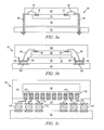
- FIG. 1 illustrates a conventional semiconductor package-on-package (PoP) 10 having a flipchip type semiconductor die 12 mounted to substrate 14 .
- Substrate 14 includes upper and lower conductive layers 16 and upper and lower insulating layers 18 .
- Bumps 20 electrically connect contact pads 22 on semiconductor die 12 to the upper conductive layer 16 .
- An underfill material 24 is deposited between semiconductor die 12 and substrate 14 and around bumps 20 .
- Semiconductor die 26 is mounted back surface-to-back surface of semiconductor die 12 with adhesive 28 .
- Bond wires 30 are formed between contact pads 32 of semiconductor die 26 and the upper conductive layer 16 .
- An encapsulant 34 is deposited over semiconductor die 12 and 26 and substrate 14 .
- a plurality of bumps 36 is formed over the lower conductive layer 16 .
- semiconductor PoP 10 One disadvantage of semiconductor PoP 10 is that substrate 14 tends to increase the overall height or profile.
- semiconductor die 12 is individually mounted to substrate 14 and then semiconductor die 26 is individually mounted to semiconductor die 12 .
- the individual stacking of semiconductor die 12 and 26 is time consuming, adds cost to the manufacturing process, and is prone to defects.
- the present invention is a method of making a semiconductor device comprising the steps of providing a carrier, mounting a first semiconductor wafer to the carrier, mounting a second semiconductor wafer to the first semiconductor wafer, singulating the first and second semiconductor wafers to separate stacked first and second semiconductor die of the first and second semiconductor wafers, forming a conductive layer over the carrier between the stacked first and second semiconductor die, forming a bond wire between contact pads on the second semiconductor die and the conductive layer, depositing an encapsulant over the stacked first and second semiconductor die, bond wire, and carrier, removing the carrier to expose the conductive layer and contact pads on the first semiconductor die, and forming bumps directly on the conductive layer and contact pads on the first semiconductor die.
- the present invention is a method of making a semiconductor device comprising the steps of providing a carrier, mounting a first wafer to the carrier, mounting a second wafer to the first wafer, singulating the first and second wafers to separate stacked first and second components of the first and second wafers, depositing a first encapsulant over the stacked first and second components and carrier, removing the carrier, and forming an interconnect structure directly on the first component.
- the present invention is a method of making a semiconductor device comprising the steps of providing a carrier, mounting a first component to the carrier, mounting a second component to the first component, depositing a first encapsulant over the first and second components and carrier, removing the carrier, and forming an interconnect structure directly on the first component.
- the present invention is a semiconductor device comprising a first component and second component mounted to the first component.
- a first encapsulant is deposited over the first and second components.
- a first interconnect structure is formed directly on the first component.
- FIG. 1 illustrates a conventional semiconductor PoP with two semiconductor die stacked over a substrate
- FIG. 2 illustrates a printed circuit board (PCB) with different types of packages mounted to its surface
- FIGS. 3 a -3 c illustrate further detail of the representative semiconductor packages mounted to the PCB
- FIGS. 4 a -4 n illustrate a process of forming a PoP with stacked semiconductor die and bumps formed directly on the lower die
- FIG. 5 illustrates the semiconductor PoP with stacked semiconductor die and bumps formed directly on the lower die
- FIGS. 6 a -6 g illustrate a method of forming a PoP with stacked semiconductor die and a protruding conductive layer and bumps formed directly on the lower die;
- FIG. 7 illustrates the semiconductor PoP with stacked semiconductor die and a protruding conductive layer and bumps formed directly on the lower die
- FIG. 8 illustrates the semiconductor PoP with a portion of the encapsulant removed to expose the upper die
- FIG. 9 illustrates the semiconductor PoP with conductive vias formed through the encapsulant
- FIG. 10 illustrates the semiconductor PoP with a TSV interposer mounted to the lower semiconductor die
- FIG. 11 illustrates the semiconductor PoP with an upper die mounted to a TSV interposer and the upper die/TSV interposer mounted to the lower die;
- FIG. 12 illustrates the semiconductor PoP with the TSV interposer exposed from the encapsulant for electrical interconnect.
- Front-end manufacturing involves the formation of a plurality of die on the surface of a semiconductor wafer.
- Each die on the wafer contains active and passive electrical components, which are electrically connected to form functional electrical circuits.
- Active electrical components such as transistors and diodes, have the ability to control the flow of electrical current.
- Passive electrical components such as capacitors, inductors, resistors, and transformers, create a relationship between voltage and current necessary to perform electrical circuit functions.
- Passive and active components are formed over the surface of the semiconductor wafer by a series of process steps including doping, deposition, photolithography, etching, and planarization.
- Doping introduces impurities into the semiconductor material by techniques such as ion implantation or thermal diffusion.
- the doping process modifies the electrical conductivity of semiconductor material in active devices, transforming the semiconductor material into an insulator, conductor, or dynamically changing the semiconductor material conductivity in response to an electric field or base current.
- Transistors contain regions of varying types and degrees of doping arranged as necessary to enable the transistor to promote or restrict the flow of electrical current upon the application of the electric field or base current.
- Active and passive components are formed by layers of materials with different electrical properties.
- the layers can be formed by a variety of deposition techniques determined in part by the type of material being deposited. For example, thin film deposition can involve chemical vapor deposition (CVD), physical vapor deposition (PVD), electrolytic plating, and electroless plating processes.
- CVD chemical vapor deposition
- PVD physical vapor deposition
- electrolytic plating electroless plating processes.
- Each layer is generally patterned to form portions of active components, passive components, or electrical connections between components.
- the layers can be patterned using photolithography, which involves the deposition of light sensitive material, e.g., photoresist, over the layer to be patterned.
- a pattern is transferred from a photomask to the photoresist using light.
- the portion of the photoresist pattern subjected to light is removed using a solvent, exposing portions of the underlying layer to be patterned.
- the portion of the photoresist pattern not subjected to light, the negative photoresist is removed using a solvent, exposing portions of the underlying layer to be patterned.
- the remainder of the photoresist is removed, leaving behind a patterned layer.
- some types of materials are patterned by directly depositing the material into the areas or voids formed by a previous deposition/etch process using techniques such as electroless and electrolytic plating.
- Planarization can be used to remove material from the surface of the wafer and produce a uniformly flat surface. Planarization involves polishing the surface of the wafer with a polishing pad. An abrasive material and corrosive chemical are added to the surface of the wafer during polishing. The combined mechanical action of the abrasive and corrosive action of the chemical removes any irregular topography, resulting in a uniformly flat surface.
- Back-end manufacturing refers to cutting or singulating the finished wafer into the individual die and then packaging the die for structural support and environmental isolation.
- the wafer is scored and broken along non-functional regions of the wafer called saw streets or scribes.
- the wafer is singulated using a laser cutting tool or saw blade.
- the individual semiconductor die are mounted to a package substrate that includes pins or contact pads for interconnection with other system components. Contact pads formed over the semiconductor die are then connected to contact pads within the package.
- the electrical connections can be made with solder bumps, stud bumps, conductive paste, or wirebonds.
- An encapsulant or other molding material is deposited over the package to provide physical support and electrical isolation.
- the finished package is then inserted into an electrical system and the functionality of the semiconductor device is made available to the other system components.
- FIG. 2 illustrates electronic device 50 having a chip carrier substrate or printed circuit board (PCB) 52 with a plurality of semiconductor packages mounted on its surface.
- Electronic device 50 can have one type of semiconductor package, or multiple types of semiconductor packages, depending on the application. The different types of semiconductor packages are shown in FIG. 2 for purposes of illustration.
- Electronic device 50 can be a stand-alone system that uses the semiconductor packages to perform one or more electrical functions.
- electronic device 50 can be a subcomponent of a larger system.
- electronic device 50 can be part of a cellular phone, personal digital assistant (PDA), digital video camera (DVC), or other electronic communication device.
- PDA personal digital assistant
- DVC digital video camera
- electronic device 50 can be a graphics card, network interface card, or other signal processing card that can be inserted into a computer.
- the semiconductor package can include microprocessors, memories, application specific integrated circuits (ASIC), logic circuits, analog circuits, RF circuits, discrete devices, or other semiconductor die or electrical components. Miniaturization and weight reduction are essential for these products to be accepted by the market. The distance between semiconductor devices must be decreased to achieve higher density.
- PCB 52 provides a general substrate for structural support and electrical interconnect of the semiconductor packages mounted on the PCB.
- Conductive signal traces 54 are formed over a surface or within layers of PCB 52 using evaporation, electrolytic plating, electroless plating, screen printing, or other suitable metal deposition process. Signal traces 54 provide for electrical communication between each of the semiconductor packages, mounted components, and other external system components. Traces 54 also provide power and ground connections to each of the semiconductor packages.
- a semiconductor device has two packaging levels.
- First level packaging is a technique for mechanically and electrically attaching the semiconductor die to an intermediate carrier.
- Second level packaging involves mechanically and electrically attaching the intermediate carrier to the PCB.
- a semiconductor device may only have the first level packaging where the die is mechanically and electrically mounted directly to the PCB.
- first level packaging including bond wire package 56 and flipchip 58
- second level packaging including ball grid array (BGA) 60 , bump chip carrier (BCC) 62 , dual in-line package (DIP) 64 , land grid array (LGA) 66 , multi-chip module (MCM) 68 , quad flat non-leaded package (QFN) 70 , and quad flat package 72 .
- BGA ball grid array
- BCC bump chip carrier
- DIP dual in-line package
- LGA land grid array
- MCM multi-chip module
- QFN quad flat non-leaded package
- quad flat package 72 quad flat package
- electronic device 50 includes a single attached semiconductor package, while other embodiments call for multiple interconnected packages.
- manufacturers can incorporate pre-made components into electronic devices and systems. Because the semiconductor packages include sophisticated functionality, electronic devices can be manufactured using cheaper components and a streamlined manufacturing process. The resulting devices are less likely to fail and less expensive to manufacture resulting in a lower cost for consumers.
- FIGS. 3 a -3 c show exemplary semiconductor packages.
- FIG. 3 a illustrates further detail of DIP 64 mounted on PCB 52 .
- Semiconductor die 74 includes an active region containing analog or digital circuits implemented as active devices, passive devices, conductive layers, and dielectric layers formed within the die and are electrically interconnected according to the electrical design of the die.
- the circuit can include one or more transistors, diodes, inductors, capacitors, resistors, and other circuit elements formed within the active region of semiconductor die 74 .
- Contact pads 76 are one or more layers of conductive material, such as aluminum (Al), copper (Cu), tin (Sn), nickel (Ni), gold (Au), or silver (Ag), and are electrically connected to the circuit elements formed within semiconductor die 74 .
- semiconductor die 74 is mounted to an intermediate carrier 78 using a gold-silicon eutectic layer or adhesive material such as thermal epoxy or epoxy resin.
- the package body includes an insulative packaging material such as polymer or ceramic.
- Conductor leads 80 and bond wires 82 provide electrical interconnect between semiconductor die 74 and PCB 52 .
- Encapsulant 84 is deposited over the package for environmental protection by preventing moisture and particles from entering the package and contaminating semiconductor die 74 or bond wires 82 .
- FIG. 3 b illustrates further detail of BCC 62 mounted on PCB 52 .
- Semiconductor die 88 is mounted over carrier 90 using an underfill or epoxy-resin adhesive material 92 .
- Bond wires 94 provide first level packaging interconnect between contact pads 96 and 98 .
- Molding compound or encapsulant 100 is deposited over semiconductor die 88 and bond wires 94 to provide physical support and electrical isolation for the device.
- Contact pads 102 are formed over a surface of PCB 52 using a suitable metal deposition process such as electrolytic plating or electroless plating to prevent oxidation.
- Contact pads 102 are electrically connected to one or more conductive signal traces 54 in PCB 52 .
- Bumps 104 are formed between contact pads 98 of BCC 62 and contact pads 102 of PCB 52 .
- semiconductor die 58 is mounted face down to intermediate carrier 106 with a flipchip style first level packaging.
- Active region 108 of semiconductor die 58 contains analog or digital circuits implemented as active devices, passive devices, conductive layers, and dielectric layers formed according to the electrical design of the die.
- the circuit can include one or more transistors, diodes, inductors, capacitors, resistors, and other circuit elements within active region 108 .
- Semiconductor die 58 is electrically and mechanically connected to carrier 106 through bumps 110 .
- BGA 60 is electrically and mechanically connected to PCB 52 with a BGA style second level packaging using bumps 112 .
- Semiconductor die 58 is electrically connected to conductive signal traces 54 in PCB 52 through bumps 110 , signal lines 114 , and bumps 112 .
- a molding compound or encapsulant 116 is deposited over semiconductor die 58 and carrier 106 to provide physical support and electrical isolation for the device.
- the flipchip semiconductor device provides a short electrical conduction path from the active devices on semiconductor die 58 to conduction tracks on PCB 52 in order to reduce signal propagation distance, lower capacitance, and improve overall circuit performance.
- the semiconductor die 58 can be mechanically and electrically connected directly to PCB 52 using flipchip style first level packaging without intermediate carrier 106 .
- FIGS. 4 a -4 n illustrate, in relation to FIGS. 2 and 3 a - 3 c , a process of forming a semiconductor PoP with stacked semiconductor die and bumps formed directly on the lower die.
- FIG. 4 a shows a semiconductor wafer 120 with a base substrate material 122 , such as silicon, germanium, gallium arsenide, indium phosphide, or silicon carbide, for structural support.
- a plurality of semiconductor die or components 124 is formed on wafer 120 separated by inter-die wafer area or saw streets 126 as described above. Saw streets 126 provide cutting areas to singulate semiconductor wafer 120 into individual semiconductor die 124 .
- FIG. 4 b shows a cross-sectional view of a portion of semiconductor wafer 120 .
- Each semiconductor die 124 has a back surface 128 and active surface 130 containing analog or digital circuits implemented as active devices, passive devices, conductive layers, and dielectric layers formed within the die and electrically interconnected according to the electrical design and function of the die.
- the circuit may include one or more transistors, diodes, and other circuit elements formed within active surface 130 to implement analog circuits or digital circuits, such as digital signal processor (DSP), ASIC, memory, or other signal processing circuit.
- DSP digital signal processor
- Semiconductor die 124 may also contain integrated passive devices (IPDs), such as inductors, capacitors, and resistors, for RF signal processing.
- IPDs integrated passive devices
- An electrically conductive layer 132 is formed over active surface 130 using PVD, CVD, electrolytic plating, electroless plating process, or other suitable metal deposition process.
- Conductive layer 132 can be one or more layers of Al, Cu, Sn, Ni, Au, Ag, or other suitable electrically conductive material.
- Conductive layer 132 operates as contact pads electrically connected to the circuits on active surface 130 .
- Contact pads 132 can be disposed side-by-side a first distance from the edge of semiconductor die 124 .
- contact pads 132 can be offset in multiple rows such that a first row of contact pads is disposed a first distance from the edge of the die, and a second row of contact pads alternating with the first row is disposed a second distance from the edge of the die.
- a temporary carrier 134 contains a sacrificial base material such as silicon, germanium, gallium arsenide, indium phosphide, silicon carbide, resin, or other suitable low-cost, rigid material for structural support.
- An interface layer or double-sided tape 136 is formed over carrier 134 as a temporary adhesive bonding film or etch-stop layer.
- Semiconductor wafer 120 is positioned over and mounted to carrier 134 and interface layer 136 , as shown in FIG. 4 c.
- FIG. 4 d shows a semiconductor wafer 140 with a base substrate material, such as silicon, germanium, gallium arsenide, indium phosphide, or silicon carbide, for structural support.
- a plurality of semiconductor die or components 144 is formed on wafer 140 separated by inter-die wafer area or saw streets 146 as described above. Saw streets 146 provide cutting areas to singulate semiconductor wafer 140 into individual semiconductor die 144 .
- Each semiconductor die 144 has a back surface 148 and active surface 150 containing analog or digital circuits implemented as active devices, passive devices, conductive layers, and dielectric layers formed within the die and electrically interconnected according to the electrical design and function of the die.
- the circuit may include one or more transistors, diodes, and other circuit elements formed within active surface 150 to implement analog circuits or digital circuits, such as DSP, ASIC, memory, or other signal processing circuit.
- Semiconductor die 144 may also contain IPDs, such as inductors, capacitors, and resistors, for RF signal processing.
- An electrically conductive layer 152 is formed over active surface 150 using PVD, CVD, electrolytic plating, electroless plating process, or other suitable metal deposition process.
- Conductive layer 152 can be one or more layers of Al, Cu, Sn, Ni, Au, Ag, or other suitable electrically conductive material. Conductive layer 152 operates as contact pads electrically connected to the circuits on active surface 150 .
- Semiconductor die 144 can have the same electrical function as semiconductor die 124 , or semiconductor die 144 can have a different electrical function than semiconductor die 124 .
- An adhesive layer 154 is formed over back surface 128 of semiconductor wafer 120 .
- Semiconductor wafer 140 is positioned over and mounted to semiconductor wafer 120 with adhesive layer 154 , as shown in FIG. 4 e .
- Saw street 126 of semiconductor wafer 120 is aligned with saw street 146 of semiconductor wafer 140 .
- semiconductor wafer 120 and semiconductor wafer 140 are singulated through saw streets 126 and 146 using a saw blade or laser cutting tool 156 into stacked semiconductor die 124 and 144 .
- a suitable cutting tool 156 can be a thick blade saw, etching saw, or water jet saw.
- FIG. 4 g the stacked semiconductor die 124 and 144 are separated using an expansion table that moves in two-dimension lateral directions, as shown by arrows 157 , to expand the spacing and create greater physical separation between the stacked semiconductor die.
- FIG. 4 h is a plan view of the expansion table moving substantially the same distance in the x-axis and y-axis by arrows 157 within the tolerance of the table control to increase width of peripheral region 159 and separation between the stacked semiconductor die 124 and 144 .
- the post-expansion width of peripheral region 159 ranges from 5-200 ⁇ m.
- an electrically conductive layer or seed layer 158 is formed over carrier 134 within peripheral region 159 between the stacked semiconductor 124 and 144 using a patterning and metal deposition process such as printing, PVD, CVD, sputtering, electrolytic plating, and electroless plating.
- Conductive layer 158 can be one or more layers of Al, Cu, Sn, Ti, Ni, Au, Ag, or other suitable electrically conductive material.
- bond wires 160 are formed between conductive layer 158 and conductive layer 152 on semiconductor die 144 .
- FIG. 4 k shows a plan view of bond wires 160 formed between conductive layer 158 and conductive layer 152 on semiconductor die 144 .
- the expanded peripheral region 159 from FIGS. 4 g -4 h provides sufficient space to form conductive layer 158 and bond wires 160 between the stack semiconductor die 124 and 144 .
- an encapsulant or molding compound 162 is deposited over semiconductor die 124 and 144 , bond wires 160 , and carrier 134 using a paste printing, compressive molding, transfer molding, liquid encapsulant molding, vacuum lamination, spin coating, or other suitable applicator.
- Encapsulant 162 can be polymer composite material, such as epoxy resin with filler, epoxy acrylate with filler, or polymer with proper filler.
- Encapsulant 162 is non-conductive and environmentally protects the semiconductor device from external elements and contaminants.
- carrier 134 and interface layer 136 are removed by chemical etching, mechanical peeling, CMP, mechanical grinding, thermal bake, UV light, laser scanning, or wet stripping to expose active surface 130 of semiconductor die 124 , conductive layers 132 and 158 , and encapsulant 162 .
- an electrically conductive bump material is deposited directly on conductive layers 132 and 158 using an evaporation, electrolytic plating, electroless plating, ball drop, or screen printing process.
- the bump material can be Al, Sn, Ni, Au, Ag, Pb, Bi, Cu, solder, and combinations thereof, with an optional flux solution.
- the bump material can be eutectic Sn/Pb, high-lead solder, or lead-free solder.
- the bump material is bonded to conductive layers 132 and 158 using a suitable attachment or bonding process. In one embodiment, the bump material is reflowed by heating the material above its melting point to form balls or bumps 164 .
- bumps 164 are reflowed a second time to improve electrical contact to conductive layers 132 and 158 .
- An under bump metallization (UBM) layer can be formed under bumps 164 .
- Bumps 164 can also be compression bonded to conductive layers 132 and 158 .
- Bumps 164 represent one type of interconnect structure that can be formed over conductive layers 132 and 158 .
- the interconnect structure can also be stud bumps, micro bumps, or other electrical interconnect.
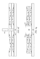
- FIG. 5 shows semiconductor PoP 168 after singulation.
- Semiconductor die 124 is electrically connected to bumps 164 .
- Semiconductor die 144 is electrically connected through bond wires 160 to conductive layer 158 and bumps 164 .
- Semiconductor die 124 and 144 are bonded at the wafer level.
- Semiconductor PoP 168 has a reduced height because bumps 164 are attached directly to conductive layer 158 and contact pads 132 of semiconductor die 124 . There is no need to mount the stacked semiconductor die to a substrate, as shown in prior art FIG. 1 .
- Carrier 134 maintains coplanarity between conductive layer 158 and contact pads 132 and uniformity of bumps 164 .
- the exposed active surface 130 of semiconductor die 124 offers good heat dissipation and thermal characteristics.
- FIGS. 6 a -6 g illustrate, in relation to FIGS. 2 and 3 a - 3 c , a process of forming a PoP with stacked semiconductor die and a protruding conductive layer and bumps formed directly on the lower die.
- a plurality of vias or cavities 170 is formed partially through carrier 134 using laser drilling, mechanic drilling, etching, or DRIE, as shown in FIG. 6 a .
- DRIE DRIE
- vias 170 are filled or lined with Al, Cu, Sn, Ni, Au, Ag, Ti, W, poly-silicon, or other suitable electrically conductive material using electrolytic plating, electroless plating process, or other suitable metal deposition process to form z-direction vertical interconnect conductive vias 172 .
- a conductive layer is conformally applied to the sidewalls and bottom surface of vias 170 by electrolytic plating or electroless plating process to form conductive vias 172 .
- bond wires 174 are formed between conductive vias 172 and conductive layer 152 on semiconductor die 144 .
- Bond wires 174 extend into cavities 170 to bond with conductive vias 172 .
- FIG. 6 d shows a plan view of bond wires 174 formed between conductive vias 172 and conductive layer 152 on semiconductor die 144 .
- the expanded peripheral region 159 from FIGS. 4 g -4 h provides sufficient space to form conductive vias 172 and bond wires 174 between the stacked semiconductor die 124 and 144 .
- an encapsulant or molding compound 176 is deposited over semiconductor die 124 and 144 , bond wires 174 , and carrier 134 using a paste printing, compressive molding, transfer molding, liquid encapsulant molding, vacuum lamination, spin coating, or other suitable applicator. Encapsulant fills the remaining portion of vias 170 not occupied by the conductive layer 172 .
- Encapsulant 176 can be polymer composite material, such as epoxy resin with filler, epoxy acrylate with filler, or polymer with proper filler. Encapsulant 176 is non-conductive and environmentally protects the semiconductor device from external elements and contaminants.
- carrier 134 and interface layer 136 are removed by chemical etching, mechanical peeling, CMP, mechanical grinding, thermal bake, UV light, laser scanning, or wet stripping to expose active surface 130 of semiconductor die 124 , conductive layer 132 , conductive vias 172 , and encapsulant 176 .
- vias 170 partially through carrier 134
- conductive vias 172 extend below or protrude beyond a level of the exposed active surface 130 of semiconductor die 124 .
- an electrically conductive bump material is deposited directly on conductive layer 132 of semiconductor die 124 using an evaporation, electrolytic plating, electroless plating, ball drop, or screen printing process.
- the bump material can be Al, Sn, Ni, Au, Ag, Pb, Bi, Cu, solder, and combinations thereof, with an optional flux solution.
- the bump material can be eutectic Sn/Pb, high-lead solder, or lead-free solder.
- the bump material is bonded to conductive layer 132 using a suitable attachment or bonding process. In one embodiment, the bump material is reflowed by heating the material above its melting point to form balls or bumps 180 .
- bumps 180 are reflowed a second time to improve electrical contact to conductive layer 132 .
- a UBM layer can be formed under bumps 180 .
- Bumps 180 can also be compression bonded to conductive layer 132 .
- Bumps 180 represent one type of interconnect structure that can be formed over conductive layer 132 .
- the interconnect structure can also be stud bumps, micro bumps, or other electrical interconnect.
- FIG. 7 shows semiconductor PoP 184 after singulation.
- Semiconductor die 124 is electrically connected to bumps 180 .
- Semiconductor die 144 is electrically connected through bond wires 174 to conductive vias 172 .
- Semiconductor die 124 and 144 are bonded at the wafer level.
- Semiconductor PoP 184 has a reduced height because bumps 180 are attached directly to contact pads 132 of semiconductor die 124 . There is no need to mount the stacked semiconductor die to a substrate, as shown in prior art FIG. 1 .
- the protruding conductive vias 172 are substantially coplanar with bumps 180 .
- the exposed active surface 130 of semiconductor die 124 offers good heat dissipation and thermal characteristics.
- FIG. 8 illustrates an embodiment of semiconductor PoP 188 , similar to FIG. 5 , with a portion of encapsulant 162 removed to expose active surface 150 of semiconductor die 144 .
- the exposed active surface 150 of semiconductor die 144 offers good heat dissipation and thermal characteristics.
- FIG. 9 illustrates an embodiment of semiconductor PoP 190 , similar to FIG. 5 , with conductive vias 192 formed through encapsulant 162 down to conductive layer 158 .
- a plurality of vias is formed through encapsulant 162 using laser drilling, mechanic drilling, etching, or DRIE.
- the vias are filled with Al, Cu, Sn, Ni, Au, Ag, Ti, W, poly-silicon, or other suitable electrically conductive material using electrolytic plating, electroless plating process, or other suitable metal deposition process to form z-direction vertical interconnect conductive vias 192 .
- Bumps 164 are formed on conductive layer 158 opposite conductive vias 192 .
- FIG. 10 illustrates an embodiment of semiconductor PoP 194 , similar to FIG. 5 , with TSV interposer or component 196 mounted to semiconductor die 124 .
- TSV interposer 196 includes substrate 198 with upper and lower conductive layers 200 and upper and lower insulating layers 202 .
- TSV interposer 196 is bonded to semiconductor die 124 with adhesive layer 204 .
- TSV interposer 196 in wafer form can be bonded to semiconductor wafer 120 over a carrier, similar to FIGS. 4 d -4 e .
- the TSV interposer wafer and semiconductor wafer 120 are singulated and the peripheral region is expanded, similar to FIGS. 4 f -4 h .
- An electrically conductive layer or seed layer 205 is formed over the carrier within the expanded peripheral region between the stacked semiconductor die and TSV interposer, similar to FIG. 4 i .
- Bond wires 206 are formed between conductive layer 200 and conductive layer 205 , similar to FIG. 4 j .
- An encapsulant or molding compound 208 is deposited over semiconductor die 124 , bond wires 206 , and TSV interposer 196 , similar to FIG. 4 l . A portion of encapsulant 208 is removed to expose upper conductive layer 200 of TSV interposer 196 for electrical interconnect.
- a plurality of bumps 209 is formed over conductive layers 132 and 205 , similar to FIG. 4 n.
- FIG. 11 illustrates an embodiment of semiconductor PoP 210 with semiconductor die or component 212 mounted to TSV interposer or component 214 .
- Semiconductor die 212 has a back surface and active surface containing analog or digital circuits implemented as active devices, passive devices, conductive layers, and dielectric layers formed within the die and electrically interconnected according to the electrical design and function of the die.
- the circuit may include one or more transistors, diodes, and other circuit elements formed within the active surface to implement analog circuits or digital circuits, such as DSP, ASIC, memory, or other signal processing circuit.
- IPDs such as inductors, capacitors, and resistors, for RF signal processing.
- TSV interposer 214 includes substrate 216 with upper and lower conductive layers 218 and upper and lower insulating layers 220 .
- Semiconductor die 212 is mounted back surface to TSV interposer 214 .
- Bond wires 222 are formed between conductive layer 218 and contact pads 224 on the active surface of semiconductor die 212 .
- An encapsulant or molding compound 226 is deposited over semiconductor die 212 , bond wires 222 , and TSV interposer 214 using a paste printing, compressive molding, transfer molding, liquid encapsulant molding, vacuum lamination, spin coating, or other suitable applicator.
- Encapsulant 226 can be polymer composite material, such as epoxy resin with filler, epoxy acrylate with filler, or polymer with proper filler.
- Encapsulant 226 is non-conductive and environmentally protects the semiconductor device from external elements and contaminants.
- An adhesive layer 228 is formed over back surface 128 of semiconductor die 124 from FIG. 4 a .
- the stacked semiconductor die 212 and TSV interposer 214 is mounted to semiconductor die 124 with encapsulant 226 bonded to adhesive layer 228 .
- the stacked semiconductor die 212 and TSV interposer 214 in wafer form can be bonded to semiconductor wafer 120 over a carrier, similar to FIGS. 4 d -4 e .
- the stacked TSV interposer/semiconductor die wafer and semiconductor wafer 120 are singulated and the peripheral region is expanded, similar to FIGS. 4 f -4 h .
- An electrically conductive layer or seed layer 230 is formed over the carrier within the expanded peripheral region between the stacked semiconductor die and TSV interposer, similar to FIG. 4 i .
- Bond wires 232 are formed between conductive layer 218 and conductive layer 230 , similar to FIG. 4 j .
- An encapsulant or molding compound 234 is deposited over semiconductor die 124 , bond wires 232 , and the stacked semiconductor die 212 and TSV interposer 214 , similar to FIG. 4 l .
- a plurality of bumps 236 is formed over conductive layers 132 and 230 , similar to FIG. 4 n.
- Semiconductor die 124 is electrically connected to bumps 236 .
- Semiconductor die 212 and TSV interposer 214 are electrically connected through bond wires 222 and 232 to conductive layer 230 and bumps 236 .
- Semiconductor die 124 and 212 and TSV interposer 214 are bonded at the wafer level.
- Semiconductor PoP 210 has a reduced height because bumps 236 are attached directly to conductive layer 230 and contact pads 132 of semiconductor die 124 .
- the carrier maintains coplanarity between conductive layer 230 and contact pads 132 and uniformity of bumps 236 .
- the exposed active surface 130 of semiconductor die 124 offers good heat dissipation and thermal characteristics.
- FIG. 12 illustrates an embodiment of semiconductor PoP 240 , similar to FIG. 11 , with a portion of encapsulant 234 removed to expose upper conductive layer 218 of TSV interposer 214 for electrical interconnect.
Abstract
Description
Claims (23)
Priority Applications (1)
| Application Number | Priority Date | Filing Date | Title |
|---|---|---|---|
| US13/195,636 US9324659B2 (en) | 2011-08-01 | 2011-08-01 | Semiconductor device and method of forming POP with stacked semiconductor die and bumps formed directly on the lower die |
Applications Claiming Priority (1)
| Application Number | Priority Date | Filing Date | Title |
|---|---|---|---|
| US13/195,636 US9324659B2 (en) | 2011-08-01 | 2011-08-01 | Semiconductor device and method of forming POP with stacked semiconductor die and bumps formed directly on the lower die |
Publications (2)
| Publication Number | Publication Date |
|---|---|
| US20130032952A1 US20130032952A1 (en) | 2013-02-07 |
| US9324659B2 true US9324659B2 (en) | 2016-04-26 |
Family
ID=47626472
Family Applications (1)
| Application Number | Title | Priority Date | Filing Date |
|---|---|---|---|
| US13/195,636 Active 2031-10-14 US9324659B2 (en) | 2011-08-01 | 2011-08-01 | Semiconductor device and method of forming POP with stacked semiconductor die and bumps formed directly on the lower die |
Country Status (1)
| Country | Link |
|---|---|
| US (1) | US9324659B2 (en) |
Cited By (4)
| Publication number | Priority date | Publication date | Assignee | Title |
|---|---|---|---|---|
| US11272618B2 (en) | 2016-04-26 | 2022-03-08 | Analog Devices International Unlimited Company | Mechanically-compliant and electrically and thermally conductive leadframes for component-on-package circuits |
| US11410977B2 (en) | 2018-11-13 | 2022-08-09 | Analog Devices International Unlimited Company | Electronic module for high power applications |
| US11749576B2 (en) | 2018-03-27 | 2023-09-05 | Analog Devices International Unlimited Company | Stacked circuit package with molded base having laser drilled openings for upper package |
| US11844178B2 (en) | 2020-06-02 | 2023-12-12 | Analog Devices International Unlimited Company | Electronic component |
Families Citing this family (11)
| Publication number | Priority date | Publication date | Assignee | Title |
|---|---|---|---|---|
| US7943421B2 (en) * | 2008-12-05 | 2011-05-17 | Taiwan Semiconductor Manufacturing Company, Ltd. | Component stacking using pre-formed adhesive films |
| US9324659B2 (en) * | 2011-08-01 | 2016-04-26 | Stats Chippac, Ltd. | Semiconductor device and method of forming POP with stacked semiconductor die and bumps formed directly on the lower die |
| KR102190390B1 (en) | 2013-11-07 | 2020-12-11 | 삼성전자주식회사 | Semiconductor package and method of fabricating the same |
| TWI584387B (en) * | 2014-08-15 | 2017-05-21 | 矽品精密工業股份有限公司 | Method of manufacturing package structure |
| US9842831B2 (en) * | 2015-05-14 | 2017-12-12 | Mediatek Inc. | Semiconductor package and fabrication method thereof |
| US10685943B2 (en) | 2015-05-14 | 2020-06-16 | Mediatek Inc. | Semiconductor chip package with resilient conductive paste post and fabrication method thereof |
| TWI782939B (en) | 2016-12-29 | 2022-11-11 | 美商英帆薩斯邦德科技有限公司 | Bonded structures with integrated passive component |
| US11114402B2 (en) * | 2018-02-23 | 2021-09-07 | Semiconductor Components Industries, Llc | Semiconductor device with backmetal and related methods |
| US11587903B2 (en) * | 2018-04-23 | 2023-02-21 | Advanced Semiconductor Engineering, Inc. | Semiconductor device package and a method of manufacturing the same |
| US11901281B2 (en) | 2019-03-11 | 2024-02-13 | Adeia Semiconductor Bonding Technologies Inc. | Bonded structures with integrated passive component |
| US11270917B2 (en) * | 2020-06-01 | 2022-03-08 | Alibaba Group Holding Limited | Scalable and flexible architectures for integrated circuit (IC) design and fabrication |
Citations (87)
| Publication number | Priority date | Publication date | Assignee | Title |
|---|---|---|---|---|
| US5424245A (en) * | 1994-01-04 | 1995-06-13 | Motorola, Inc. | Method of forming vias through two-sided substrate |
| US6229217B1 (en) | 1998-01-14 | 2001-05-08 | Sharp Kabushiki Kaisha | Semiconductor device and method of manufacturing the same |
| US20020045290A1 (en) * | 1996-02-20 | 2002-04-18 | Michael B. Ball | Flip chip and conventional stack |
| US6552426B2 (en) * | 2000-05-10 | 2003-04-22 | Sharp Kabushiki Kaisha | Semiconductor device and method of manufacturing same |
| US6670206B2 (en) * | 2001-12-07 | 2003-12-30 | Samsung Electro-Mechanics Co., Ltd. | Method for fabricating surface acoustic wave filter packages |
| US20040103509A1 (en) * | 1998-12-08 | 2004-06-03 | Agnes Bidard | Encapsulated surface acoustic wave component and method of collective fabrication |
| US6768190B2 (en) * | 2002-01-25 | 2004-07-27 | Advanced Semiconductor Engineering, Inc. | Stack type flip-chip package |
| US20050133932A1 (en) * | 2003-12-19 | 2005-06-23 | Jens Pohl | Semiconductor module with a semiconductor stack, and methods for its production |
| US20050212126A1 (en) * | 2002-11-05 | 2005-09-29 | Shinko Electric Industries Co., Ltd. | Semiconductor device and method of manufacturing the same |
| US20060043573A1 (en) * | 2004-08-30 | 2006-03-02 | Harry Hedler | Semiconductor and method for producing a semiconductor |
| US7026709B2 (en) | 2003-04-18 | 2006-04-11 | Advanced Semiconductor Engineering Inc. | Stacked chip-packaging structure |
| US20060227587A1 (en) * | 2005-03-22 | 2006-10-12 | Satoshi Nakamura | Multichip package or system-in package |
| US7208335B2 (en) * | 2003-09-30 | 2007-04-24 | Micron Technology, Inc. | Castellated chip-scale packages and methods for fabricating the same |
| US20070108605A1 (en) | 2005-04-23 | 2007-05-17 | Stats Chippac Ltd. | Bump chip carrier semiconductor package system |
| US7221041B2 (en) | 2003-07-29 | 2007-05-22 | Advanced Semiconductor Engineering, Inc. | Multi-chips module package and manufacturing method thereof |
| US20080054451A1 (en) * | 2006-09-06 | 2008-03-06 | Michael Bauer | Multi-chip assembly |
| US20080145589A1 (en) | 2006-12-19 | 2008-06-19 | Advanced Semiconductor Engineering, Inc. | Electronic package |
| US20080272464A1 (en) * | 2007-05-04 | 2008-11-06 | Stats Chippac, Ltd. | Semiconductor Wafer Having Through-Hole Vias on Saw Streets with Backside Redistribution Layer |
| US20080272470A1 (en) * | 2007-05-04 | 2008-11-06 | Stats Chippac, Ltd. | Same Size Through-Hole Via Die Stacked Package |
| US20080272465A1 (en) * | 2007-05-04 | 2008-11-06 | Stats Chippac, Ltd. | Semiconductor Die with Through-Hole Via on Saw Streets and Through-Hole Via in Active Area of Die |
| US20080272476A1 (en) * | 2007-05-04 | 2008-11-06 | Stats Chippac, Ltd. | Through-Hole Via On Saw Streets |
| US20080272504A1 (en) * | 2007-05-04 | 2008-11-06 | Stats Chippac, Ltd. | Package-in-Package Using Through-Hole via Die on Saw Streets |
| US20080272368A1 (en) * | 2007-05-04 | 2008-11-06 | Stats Chippac, Ltd. | Extended Redistribution Layers Bumped Wafer |
| US20080272477A1 (en) * | 2007-05-04 | 2008-11-06 | Stats Chippac, Ltd. | Package-on-Package Using Through-Hole Via Die on Saw Streets |
| US20090008793A1 (en) * | 2007-07-02 | 2009-01-08 | Infineon Technologies Ag | Semiconductor device |
| US20090039523A1 (en) * | 2007-08-07 | 2009-02-12 | Tongbi Jiang | Packaged integrated circuit devices with through-body conductive vias, and methods of making same |
| US20090085225A1 (en) * | 2007-10-02 | 2009-04-02 | Samsung Electronics Co., Ltd. | Semiconductor packages having interposers, electronic products employing the same, and methods of manufacturing the same |
| US20090085186A1 (en) * | 2007-09-28 | 2009-04-02 | Infineon Technologies Ag | Semiconductor Device and Methods of Manufacturing Semiconductor Devices |
| US20090108428A1 (en) | 2007-10-29 | 2009-04-30 | Flynn Carson | Mountable integrated circuit package system with substrate having a conductor-free recess |
| US20090127683A1 (en) | 2007-11-16 | 2009-05-21 | Byung Tai Do | Integrated circuit package system with insulator |
| US20090130840A1 (en) * | 2007-11-16 | 2009-05-21 | Chung Yu Wang | Protected Solder Ball Joints in Wafer Level Chip-Scale Packaging |
| US20090127686A1 (en) * | 2007-11-21 | 2009-05-21 | Advanced Chip Engineering Technology Inc. | Stacking die package structure for semiconductor devices and method of the same |
| US20090152740A1 (en) | 2007-12-17 | 2009-06-18 | Soo-San Park | Integrated circuit package system with flip chip |
| US20090224391A1 (en) * | 2008-03-04 | 2009-09-10 | Stats Chippac, Ltd. | Wafer Level Die Integration and Method Therefor |
| US20090230531A1 (en) * | 2008-03-13 | 2009-09-17 | Stats Chippac, Ltd. | Semiconductor Package with Penetrable Encapsulant Joining Semiconductor Die and Method Thereof |
| US20090236686A1 (en) * | 2006-04-19 | 2009-09-24 | Stats Chippac, Ltd. | Semiconductor Device and Method of Forming UBM Fixed Relative to Interconnect Structure for Alignment of Semiconductor Die |
| US20090243045A1 (en) * | 2008-03-27 | 2009-10-01 | Stats Chippac, Ltd. | Through Hole Vias at Saw Streets Including Protrusions or Recesses for Interconnection |
| US20090261466A1 (en) * | 2006-11-10 | 2009-10-22 | Stats Chippac, Ltd. | Semiconductor Device and Method of Forming Vertical Interconnect Structure Using Stud Bumps |
| US7618846B1 (en) * | 2008-06-16 | 2009-11-17 | Stats Chippac, Ltd. | Semiconductor device and method of forming shielding along a profile disposed in peripheral region around the device |
| US20090283870A1 (en) * | 2008-05-15 | 2009-11-19 | Stats Chippac, Ltd. | Semiconductor Device and Method of Conforming Conductive Vias Between Insulating Layers in Saw Streets |
| US20090294899A1 (en) * | 2008-05-27 | 2009-12-03 | Stats Chippac, Ltd. | Semiconductor device and method of forming embedded passive circuit elements interconnected to through hole vias |
| US20090294914A1 (en) * | 2008-05-27 | 2009-12-03 | Stats Chippac, Ltd. | Semiconductor Device and Method of Forming Through Vias with Reflowed Conductive Material |
| US20090294911A1 (en) * | 2008-05-27 | 2009-12-03 | Stats Chippac, Ltd. | Semiconductor Device and Method of Forming Double-Sided Through Vias in Saw Streets |
| US20090302478A1 (en) * | 2008-06-04 | 2009-12-10 | Stats Chippac, Ltd. | Semiconductor device and method of forming recessed conductive vias in saw streets |
| US20090302445A1 (en) * | 2008-06-09 | 2009-12-10 | Stats Chippac, Ltd. | Method and Apparatus for Thermally Enhanced Semiconductor Package |
| US20090302435A1 (en) * | 2008-06-04 | 2009-12-10 | Stats Chippac, Ltd. | Semiconductor Device and Method of Shielding Semiconductor Die from Inter-Device Interference |
| US20100007000A1 (en) | 2008-07-11 | 2010-01-14 | Kim Youngjoon | Package stacking system with mold contamination prevention |
| US20100007029A1 (en) * | 2008-07-14 | 2010-01-14 | Stats Chippac, Ltd. | Semiconductor device and method of forming stepped-down rdl and recessed thv in peripheral region of the device |
| US20100013102A1 (en) * | 2008-07-15 | 2010-01-21 | Stats Chippac, Ltd. | Semiconductor Device and Method of Providing a Thermal Dissipation Path Through RDL and Conductive Via |
| US20100078828A1 (en) | 2008-09-27 | 2010-04-01 | Rui Huang | Integrated circuit package system with mounting structure |
| US20100102458A1 (en) | 2008-10-28 | 2010-04-29 | Seng Guan Chow | Semiconductor package system with cavity substrate and manufacturing method therefor |
| US20100123251A1 (en) | 2008-11-19 | 2010-05-20 | Seng Guan Chow | Integrated circuit packaging system with multi level contact and method of manufacture thereof |
| US20100140780A1 (en) * | 2008-12-10 | 2010-06-10 | Stats Chippac, Ltd. | Semiconductor Device and Method of Forming an IPD Beneath a Semiconductor Die with Direct Connection to External Devices |
| US20100140751A1 (en) * | 2008-12-10 | 2010-06-10 | Stats Chippac, Ltd. | Semiconductor Device and Method of Forming a Conductive Via-in-Via Structure |
| US7759783B2 (en) | 2006-12-07 | 2010-07-20 | Stats Chippac Ltd. | Integrated circuit package system employing thin profile techniques |
| US7776655B2 (en) * | 2008-12-10 | 2010-08-17 | Stats Chippac, Ltd. | Semiconductor device and method of forming conductive pillars in recessed region of peripheral area around the device for electrical interconnection to other devices |
| US20100230822A1 (en) * | 2009-03-13 | 2010-09-16 | Stats Chippac, Ltd. | Semiconductor Die and Method of Forming Noise Absorbing Regions Between THVS in Peripheral Region of the Die |
| US20100233852A1 (en) * | 2007-05-04 | 2010-09-16 | Stats Chippac, Ltd. | Semiconductor Device and Method of Stacking Same Size Semiconductor Die Electrically Connected Through Conductive Via Formed Around Periphery of the Die |
| US20100237471A1 (en) * | 2009-03-17 | 2010-09-23 | Stats Chippac, Ltd. | Semiconductor Die and Method of Forming Through Organic Vias Having Varying Width in Peripheral Region of the Die |
| US7855100B2 (en) * | 2005-03-31 | 2010-12-21 | Stats Chippac Ltd. | Integrated circuit package system with an encapsulant cavity and method of fabrication thereof |
| US7859099B2 (en) * | 2008-12-11 | 2010-12-28 | Stats Chippac Ltd. | Integrated circuit packaging system having through silicon via with direct interconnects and method of manufacture thereof |
| US20110123251A1 (en) | 2005-09-26 | 2011-05-26 | Beifa Group Co., Ltd. | Casing for a writing instrument and method of manufacturing the same using a dual injection molding |
| US7956449B2 (en) * | 2008-06-25 | 2011-06-07 | Stats Chippac Ltd. | Stacked integrated circuit package system |
| US7982298B1 (en) * | 2008-12-03 | 2011-07-19 | Amkor Technology, Inc. | Package in package semiconductor device |
| US20110177654A1 (en) * | 2010-01-21 | 2011-07-21 | Advanced Semiconductor Engineering, Inc. | Wafer-Level Semiconductor Device Packages with Three-Dimensional Fan-Out and Manufacturing Methods Thereof |
| US20110227220A1 (en) * | 2010-03-22 | 2011-09-22 | Chia-Ching Chen | Stackable semiconductor package and manufacturing method thereof |
| US20110278741A1 (en) * | 2010-05-14 | 2011-11-17 | Stats Chippac, Ltd. | Semiconductor Device and Method of Forming Interconnect Structure and Mounting Semiconductor Die in Recessed Encapsulant |
| US20110316133A1 (en) | 2010-06-24 | 2011-12-29 | Byung Tai Do | Integrated circuit package system with package stand-off and method of manufacture thereof |
| US20120018885A1 (en) * | 2010-07-26 | 2012-01-26 | Go Eun Lee | Semiconductor apparatus having through vias |
| US20120032340A1 (en) * | 2010-08-06 | 2012-02-09 | Stats Chippac, Ltd. | Semiconductor Die and Method of Forming FO-WLCSP Vertical Interconnect Using TSV and TMV |
| US8203203B1 (en) * | 2006-11-16 | 2012-06-19 | Amkor Technology, Inc. | Stacked redistribution layer (RDL) die assembly package |
| US8227338B1 (en) * | 2004-03-23 | 2012-07-24 | Amkor Technology, Inc. | Semiconductor package including a top-surface metal layer for implementing circuit features |
| US20120196406A1 (en) * | 2006-11-10 | 2012-08-02 | Stats Chippac, Ltd. | Semiconductor Package with Embedded Die |
| US20120217629A1 (en) * | 2011-02-25 | 2012-08-30 | Stats Chippac, Ltd. | Semiconductor Device and Method of Forming a Wafer Level Package Structure Using Conductive Via and Exposed Bump |
| US20120217643A1 (en) * | 2011-02-24 | 2012-08-30 | Stats Chippac, Ltd. | Semiconductor Device and Method of Forming Bond Wires Between Semiconductor Die Contact Pads and Conductive TOV in Peripheral Area Around Semiconductor Die |
| US8258012B2 (en) * | 2010-05-14 | 2012-09-04 | Stats Chippac, Ltd. | Semiconductor device and method of forming discontinuous ESD protection layers between semiconductor die |
| US8273604B2 (en) * | 2011-02-22 | 2012-09-25 | STAT ChipPAC, Ltd. | Semiconductor device and method of forming WLCSP structure using protruded MLP |
| US8278746B2 (en) * | 2010-04-02 | 2012-10-02 | Advanced Semiconductor Engineering, Inc. | Semiconductor device packages including connecting elements |
| US8304286B2 (en) * | 2009-12-11 | 2012-11-06 | Stats Chippac Ltd. | Integrated circuit packaging system with shielded package and method of manufacture thereof |
| US8341835B1 (en) * | 2002-05-01 | 2013-01-01 | Amkor Technology, Inc. | Buildup dielectric layer having metallization pattern semiconductor package fabrication method |
| US20130032952A1 (en) * | 2011-08-01 | 2013-02-07 | Stats Chippac, Ltd. | Semiconductor Device and Method of Forming POP With Stacked Semiconductor Die and Bumps Formed Directly on the Lower Die |
| US8405197B2 (en) * | 2009-03-25 | 2013-03-26 | Stats Chippac Ltd. | Integrated circuit packaging system with stacked configuration and method of manufacture thereof |
| US8471376B1 (en) * | 2009-05-06 | 2013-06-25 | Marvell International Ltd. | Integrated circuit packaging configurations |
| US8518746B2 (en) * | 2010-09-02 | 2013-08-27 | Stats Chippac, Ltd. | Semiconductor device and method of forming TSV semiconductor wafer with embedded semiconductor die |
| US8623702B2 (en) * | 2011-02-24 | 2014-01-07 | Stats Chippac, Ltd. | Semiconductor device and method of forming conductive THV and RDL on opposite sides of semiconductor die for RDL-to-RDL bonding |
| US8796137B2 (en) * | 2010-06-24 | 2014-08-05 | Stats Chippac, Ltd. | Semiconductor device and method of forming RDL along sloped side surface of semiconductor die for z-direction interconnect |
| US8822281B2 (en) * | 2010-02-23 | 2014-09-02 | Stats Chippac, Ltd. | Semiconductor device and method of forming TMV and TSV in WLCSP using same carrier |
-
2011
- 2011-08-01 US US13/195,636 patent/US9324659B2/en active Active
Patent Citations (140)
| Publication number | Priority date | Publication date | Assignee | Title |
|---|---|---|---|---|
| US5424245A (en) * | 1994-01-04 | 1995-06-13 | Motorola, Inc. | Method of forming vias through two-sided substrate |
| US20020045290A1 (en) * | 1996-02-20 | 2002-04-18 | Michael B. Ball | Flip chip and conventional stack |
| US6229217B1 (en) | 1998-01-14 | 2001-05-08 | Sharp Kabushiki Kaisha | Semiconductor device and method of manufacturing the same |
| US20040103509A1 (en) * | 1998-12-08 | 2004-06-03 | Agnes Bidard | Encapsulated surface acoustic wave component and method of collective fabrication |
| US6552426B2 (en) * | 2000-05-10 | 2003-04-22 | Sharp Kabushiki Kaisha | Semiconductor device and method of manufacturing same |
| US6670206B2 (en) * | 2001-12-07 | 2003-12-30 | Samsung Electro-Mechanics Co., Ltd. | Method for fabricating surface acoustic wave filter packages |
| US6768190B2 (en) * | 2002-01-25 | 2004-07-27 | Advanced Semiconductor Engineering, Inc. | Stack type flip-chip package |
| US8341835B1 (en) * | 2002-05-01 | 2013-01-01 | Amkor Technology, Inc. | Buildup dielectric layer having metallization pattern semiconductor package fabrication method |
| US20050212126A1 (en) * | 2002-11-05 | 2005-09-29 | Shinko Electric Industries Co., Ltd. | Semiconductor device and method of manufacturing the same |
| US7026709B2 (en) | 2003-04-18 | 2006-04-11 | Advanced Semiconductor Engineering Inc. | Stacked chip-packaging structure |
| US7221041B2 (en) | 2003-07-29 | 2007-05-22 | Advanced Semiconductor Engineering, Inc. | Multi-chips module package and manufacturing method thereof |
| US7208335B2 (en) * | 2003-09-30 | 2007-04-24 | Micron Technology, Inc. | Castellated chip-scale packages and methods for fabricating the same |
| US20050133932A1 (en) * | 2003-12-19 | 2005-06-23 | Jens Pohl | Semiconductor module with a semiconductor stack, and methods for its production |
| US8227338B1 (en) * | 2004-03-23 | 2012-07-24 | Amkor Technology, Inc. | Semiconductor package including a top-surface metal layer for implementing circuit features |
| US20060043573A1 (en) * | 2004-08-30 | 2006-03-02 | Harry Hedler | Semiconductor and method for producing a semiconductor |
| US20060227587A1 (en) * | 2005-03-22 | 2006-10-12 | Satoshi Nakamura | Multichip package or system-in package |
| US7855100B2 (en) * | 2005-03-31 | 2010-12-21 | Stats Chippac Ltd. | Integrated circuit package system with an encapsulant cavity and method of fabrication thereof |
| US20070108605A1 (en) | 2005-04-23 | 2007-05-17 | Stats Chippac Ltd. | Bump chip carrier semiconductor package system |
| US20110123251A1 (en) | 2005-09-26 | 2011-05-26 | Beifa Group Co., Ltd. | Casing for a writing instrument and method of manufacturing the same using a dual injection molding |
| US20090236686A1 (en) * | 2006-04-19 | 2009-09-24 | Stats Chippac, Ltd. | Semiconductor Device and Method of Forming UBM Fixed Relative to Interconnect Structure for Alignment of Semiconductor Die |
| US20080054451A1 (en) * | 2006-09-06 | 2008-03-06 | Michael Bauer | Multi-chip assembly |
| US20120196406A1 (en) * | 2006-11-10 | 2012-08-02 | Stats Chippac, Ltd. | Semiconductor Package with Embedded Die |
| US8193034B2 (en) * | 2006-11-10 | 2012-06-05 | Stats Chippac, Ltd. | Semiconductor device and method of forming vertical interconnect structure using stud bumps |
| US8525337B2 (en) * | 2006-11-10 | 2013-09-03 | Stats Chippac, Ltd. | Semiconductor device and method of forming stud bumps over embedded die |
| US20130292829A1 (en) * | 2006-11-10 | 2013-11-07 | Stats Chippac, Ltd. | Semiconductor Package with Embedded Die |
| US20090261466A1 (en) * | 2006-11-10 | 2009-10-22 | Stats Chippac, Ltd. | Semiconductor Device and Method of Forming Vertical Interconnect Structure Using Stud Bumps |
| US8203203B1 (en) * | 2006-11-16 | 2012-06-19 | Amkor Technology, Inc. | Stacked redistribution layer (RDL) die assembly package |
| US7759783B2 (en) | 2006-12-07 | 2010-07-20 | Stats Chippac Ltd. | Integrated circuit package system employing thin profile techniques |
| US20080145589A1 (en) | 2006-12-19 | 2008-06-19 | Advanced Semiconductor Engineering, Inc. | Electronic package |
| US7687318B2 (en) * | 2007-05-04 | 2010-03-30 | Stats Chippac, Ltd. | Extended redistribution layers bumped wafer |
| US20120244661A9 (en) * | 2007-05-04 | 2012-09-27 | Stats Chippac, Ltd. | Method of Fabricating Semiconductor Die with Through-Hole Via on Saw Streets and Through-Hole Via in Active Area of Die |
| US8247268B2 (en) * | 2007-05-04 | 2012-08-21 | Stats Chippac, Ltd. | Semiconductor wafer having through-hole vias on saw streets with backside redistribution layer |
| US20120199963A9 (en) * | 2007-05-04 | 2012-08-09 | Stats Chippac, Ltd. | Package-on-Package Using Through-Hole Via Die on Saw Streets |
| US7569421B2 (en) * | 2007-05-04 | 2009-08-04 | Stats Chippac, Ltd. | Through-hole via on saw streets |
| US7750452B2 (en) * | 2007-05-04 | 2010-07-06 | Stats Chippac, Ltd. | Same size die stacked package having through-hole vias formed in organic material |
| US8815643B2 (en) * | 2007-05-04 | 2014-08-26 | Stats Chippac, Ltd. | Method of fabricating semiconductor die with through-hole via on saw streets and through-hole via in active area of die |
| US20080272464A1 (en) * | 2007-05-04 | 2008-11-06 | Stats Chippac, Ltd. | Semiconductor Wafer Having Through-Hole Vias on Saw Streets with Backside Redistribution Layer |
| US8716853B2 (en) * | 2007-05-04 | 2014-05-06 | Stats Chippac, Ltd. | Extended redistribution layers bumped wafer |
| US20080272368A1 (en) * | 2007-05-04 | 2008-11-06 | Stats Chippac, Ltd. | Extended Redistribution Layers Bumped Wafer |
| US20090267236A1 (en) * | 2007-05-04 | 2009-10-29 | Stats Chicpac, Ltd. | Through-Hole Via on Saw Streets |
| US7902638B2 (en) * | 2007-05-04 | 2011-03-08 | Stats Chippac, Ltd. | Semiconductor die with through-hole via on saw streets and through-hole via in active area of die |
| US20100233852A1 (en) * | 2007-05-04 | 2010-09-16 | Stats Chippac, Ltd. | Semiconductor Device and Method of Stacking Same Size Semiconductor Die Electrically Connected Through Conductive Via Formed Around Periphery of the Die |
| US8445325B2 (en) * | 2007-05-04 | 2013-05-21 | Stats Chippac, Ltd. | Package-in-package using through-hole via die on saw streets |
| US20080272477A1 (en) * | 2007-05-04 | 2008-11-06 | Stats Chippac, Ltd. | Package-on-Package Using Through-Hole Via Die on Saw Streets |
| US7829998B2 (en) * | 2007-05-04 | 2010-11-09 | Stats Chippac, Ltd. | Semiconductor wafer having through-hole vias on saw streets with backside redistribution layer |
| US7723159B2 (en) * | 2007-05-04 | 2010-05-25 | Stats Chippac, Ltd. | Package-on-package using through-hole via die on saw streets |
| US20100140799A1 (en) * | 2007-05-04 | 2010-06-10 | Stats Chippac, Ltd. | Extended Redistribution Layers Bumped Wafer |
| US20100193931A1 (en) * | 2007-05-04 | 2010-08-05 | Stats Chippac, Ltd. | Package-on-Package Using Through-Hole Via Die on Saw Streets |
| US20080272504A1 (en) * | 2007-05-04 | 2008-11-06 | Stats Chippac, Ltd. | Package-in-Package Using Through-Hole via Die on Saw Streets |
| US20080272476A1 (en) * | 2007-05-04 | 2008-11-06 | Stats Chippac, Ltd. | Through-Hole Via On Saw Streets |
| US20080272465A1 (en) * | 2007-05-04 | 2008-11-06 | Stats Chippac, Ltd. | Semiconductor Die with Through-Hole Via on Saw Streets and Through-Hole Via in Active Area of Die |
| US8062929B2 (en) * | 2007-05-04 | 2011-11-22 | Stats Chippac, Ltd. | Semiconductor device and method of stacking same size semiconductor die electrically connected through conductive via formed around periphery of the die |
| US7960841B2 (en) * | 2007-05-04 | 2011-06-14 | Stats Chippac, Ltd. | Through-hole via on saw streets |
| US20110124156A1 (en) * | 2007-05-04 | 2011-05-26 | Stats Chippac, Ltd. | Method of Fabricating Semiconductor Die with Through-Hole Via on Saw Streets and Through-Hole Via in Active Area of Die |
| US20080272470A1 (en) * | 2007-05-04 | 2008-11-06 | Stats Chippac, Ltd. | Same Size Through-Hole Via Die Stacked Package |
| US20110111591A1 (en) * | 2007-05-04 | 2011-05-12 | Stats Chippac, Ltd. | Semiconductor Wafer Having Through-Hole Vias on Saw Streets With Backside Redistribution Layer |
| US20090008793A1 (en) * | 2007-07-02 | 2009-01-08 | Infineon Technologies Ag | Semiconductor device |
| US20090039523A1 (en) * | 2007-08-07 | 2009-02-12 | Tongbi Jiang | Packaged integrated circuit devices with through-body conductive vias, and methods of making same |
| US20090085186A1 (en) * | 2007-09-28 | 2009-04-02 | Infineon Technologies Ag | Semiconductor Device and Methods of Manufacturing Semiconductor Devices |
| US20090085225A1 (en) * | 2007-10-02 | 2009-04-02 | Samsung Electronics Co., Ltd. | Semiconductor packages having interposers, electronic products employing the same, and methods of manufacturing the same |
| US20090108428A1 (en) | 2007-10-29 | 2009-04-30 | Flynn Carson | Mountable integrated circuit package system with substrate having a conductor-free recess |
| US20090127683A1 (en) | 2007-11-16 | 2009-05-21 | Byung Tai Do | Integrated circuit package system with insulator |
| US20090130840A1 (en) * | 2007-11-16 | 2009-05-21 | Chung Yu Wang | Protected Solder Ball Joints in Wafer Level Chip-Scale Packaging |
| US20090127686A1 (en) * | 2007-11-21 | 2009-05-21 | Advanced Chip Engineering Technology Inc. | Stacking die package structure for semiconductor devices and method of the same |
| US20090152740A1 (en) | 2007-12-17 | 2009-06-18 | Soo-San Park | Integrated circuit package system with flip chip |
| US20090224391A1 (en) * | 2008-03-04 | 2009-09-10 | Stats Chippac, Ltd. | Wafer Level Die Integration and Method Therefor |
| US20090230531A1 (en) * | 2008-03-13 | 2009-09-17 | Stats Chippac, Ltd. | Semiconductor Package with Penetrable Encapsulant Joining Semiconductor Die and Method Thereof |
| US8072079B2 (en) * | 2008-03-27 | 2011-12-06 | Stats Chippac, Ltd. | Through hole vias at saw streets including protrusions or recesses for interconnection |
| US20090243045A1 (en) * | 2008-03-27 | 2009-10-01 | Stats Chippac, Ltd. | Through Hole Vias at Saw Streets Including Protrusions or Recesses for Interconnection |
| US8030136B2 (en) * | 2008-05-15 | 2011-10-04 | Stats Chippac, Ltd. | Semiconductor device and method of conforming conductive vias between insulating layers in saw streets |
| US20090283870A1 (en) * | 2008-05-15 | 2009-11-19 | Stats Chippac, Ltd. | Semiconductor Device and Method of Conforming Conductive Vias Between Insulating Layers in Saw Streets |
| US20090294914A1 (en) * | 2008-05-27 | 2009-12-03 | Stats Chippac, Ltd. | Semiconductor Device and Method of Forming Through Vias with Reflowed Conductive Material |
| US7666711B2 (en) * | 2008-05-27 | 2010-02-23 | Stats Chippac, Ltd. | Semiconductor device and method of forming double-sided through vias in saw streets |
| US20100213618A1 (en) * | 2008-05-27 | 2010-08-26 | Stats Chippac, Ltd. | Semiconductor Device and Method of Forming Through Vias with Reflowed Conductive Material |
| US20100216281A1 (en) * | 2008-05-27 | 2010-08-26 | Stats Chippac, Ltd. | Semiconductor Device and Method of Forming Through Vias with Reflowed Conductive Material |
| US20100102456A1 (en) * | 2008-05-27 | 2010-04-29 | Stats Chippac, Ltd. | Semiconductor Device and Method of Forming Double-Sided Through Vias in Saw Streets |
| US7741156B2 (en) * | 2008-05-27 | 2010-06-22 | Stats Chippac, Ltd. | Semiconductor device and method of forming through vias with reflowed conductive material |
| US8592950B2 (en) * | 2008-05-27 | 2013-11-26 | Stats Chippac, Ltd. | Semiconductor device and method of forming through vias with reflowed conductive material |
| US20090294911A1 (en) * | 2008-05-27 | 2009-12-03 | Stats Chippac, Ltd. | Semiconductor Device and Method of Forming Double-Sided Through Vias in Saw Streets |
| US7648911B2 (en) * | 2008-05-27 | 2010-01-19 | Stats Chippac, Ltd. | Semiconductor device and method of forming embedded passive circuit elements interconnected to through hole vias |
| US20100072570A1 (en) * | 2008-05-27 | 2010-03-25 | Stats Chippac, Ltd. | Semiconductor Device and Method of Forming Embedded Passive Circuit Elements Interconnected to Through Hole Vias |
| US7859085B2 (en) * | 2008-05-27 | 2010-12-28 | Stats Chippac, Ltd. | Semiconductor device and method of forming embedded passive circuit elements interconnected to through hole vias |
| US20090294899A1 (en) * | 2008-05-27 | 2009-12-03 | Stats Chippac, Ltd. | Semiconductor device and method of forming embedded passive circuit elements interconnected to through hole vias |
| US8492201B2 (en) * | 2008-05-27 | 2013-07-23 | Stats Chippac, Ltd. | Semiconductor device and method of forming through vias with reflowed conductive material |
| US8101460B2 (en) * | 2008-06-04 | 2012-01-24 | Stats Chippac, Ltd. | Semiconductor device and method of shielding semiconductor die from inter-device interference |
| US20090302478A1 (en) * | 2008-06-04 | 2009-12-10 | Stats Chippac, Ltd. | Semiconductor device and method of forming recessed conductive vias in saw streets |
| US20090302435A1 (en) * | 2008-06-04 | 2009-12-10 | Stats Chippac, Ltd. | Semiconductor Device and Method of Shielding Semiconductor Die from Inter-Device Interference |
| US7704796B2 (en) * | 2008-06-04 | 2010-04-27 | Stats Chippac, Ltd. | Semiconductor device and method of forming recessed conductive vias in saw streets |
| US20100155922A1 (en) * | 2008-06-04 | 2010-06-24 | Stats Chippac, Ltd. | Semiconductor Device and Method of Forming Recessed Conductive Vias in Saw Streets |
| US20090302445A1 (en) * | 2008-06-09 | 2009-12-10 | Stats Chippac, Ltd. | Method and Apparatus for Thermally Enhanced Semiconductor Package |
| US7880275B2 (en) * | 2008-06-16 | 2011-02-01 | Stats Chippac, Ltd. | Semiconductor device and method of forming shielding along a profile disposed in peripheral region around the device |
| US20100019359A1 (en) * | 2008-06-16 | 2010-01-28 | Stats Chippac, Ltd. | Semiconductor Device and Method of Forming Shielding Along a Profile Disposed in Peripheral Region Around the Device |
| US7618846B1 (en) * | 2008-06-16 | 2009-11-17 | Stats Chippac, Ltd. | Semiconductor device and method of forming shielding along a profile disposed in peripheral region around the device |
| US7956449B2 (en) * | 2008-06-25 | 2011-06-07 | Stats Chippac Ltd. | Stacked integrated circuit package system |
| US20100007000A1 (en) | 2008-07-11 | 2010-01-14 | Kim Youngjoon | Package stacking system with mold contamination prevention |
| US7659145B2 (en) * | 2008-07-14 | 2010-02-09 | Stats Chippac, Ltd. | Semiconductor device and method of forming stepped-down RDL and recessed THV in peripheral region of the device |
| US20100096731A1 (en) * | 2008-07-14 | 2010-04-22 | Stats Chippac, Ltd. | Semiconductor Device and Method of Forming Stepped-Down RDL and Recessed THV in Peripheral Region of the Device |
| US20100007029A1 (en) * | 2008-07-14 | 2010-01-14 | Stats Chippac, Ltd. | Semiconductor device and method of forming stepped-down rdl and recessed thv in peripheral region of the device |
| US8080882B2 (en) * | 2008-07-14 | 2011-12-20 | Stats Chippac, Ltd. | Semiconductor device and method of forming stepped-down RDL and recessed THV in peripheral region of the device |
| US7842607B2 (en) * | 2008-07-15 | 2010-11-30 | Stats Chippac, Ltd. | Semiconductor device and method of providing a thermal dissipation path through RDL and conductive via |
| US20100013102A1 (en) * | 2008-07-15 | 2010-01-21 | Stats Chippac, Ltd. | Semiconductor Device and Method of Providing a Thermal Dissipation Path Through RDL and Conductive Via |
| US8174098B2 (en) * | 2008-07-15 | 2012-05-08 | Stats Chippac, Ltd. | Semiconductor device and method of providing a thermal dissipation path through RDL and conductive via |
| US20110037168A1 (en) * | 2008-07-15 | 2011-02-17 | Stats Chippac, Ltd. | Semiconductor Device and Method of Providing a Thermal Dissipation Path Through RDL and Conductive Via |
| US20100078828A1 (en) | 2008-09-27 | 2010-04-01 | Rui Huang | Integrated circuit package system with mounting structure |
| US20100102458A1 (en) | 2008-10-28 | 2010-04-29 | Seng Guan Chow | Semiconductor package system with cavity substrate and manufacturing method therefor |
| US8080885B2 (en) * | 2008-11-19 | 2011-12-20 | Stats Chippac Ltd. | Integrated circuit packaging system with multi level contact and method of manufacture thereof |
| US20100123251A1 (en) | 2008-11-19 | 2010-05-20 | Seng Guan Chow | Integrated circuit packaging system with multi level contact and method of manufacture thereof |
| US7982298B1 (en) * | 2008-12-03 | 2011-07-19 | Amkor Technology, Inc. | Package in package semiconductor device |
| US20100140751A1 (en) * | 2008-12-10 | 2010-06-10 | Stats Chippac, Ltd. | Semiconductor Device and Method of Forming a Conductive Via-in-Via Structure |
| US7776655B2 (en) * | 2008-12-10 | 2010-08-17 | Stats Chippac, Ltd. | Semiconductor device and method of forming conductive pillars in recessed region of peripheral area around the device for electrical interconnection to other devices |
| US20100140780A1 (en) * | 2008-12-10 | 2010-06-10 | Stats Chippac, Ltd. | Semiconductor Device and Method of Forming an IPD Beneath a Semiconductor Die with Direct Connection to External Devices |
| US8283250B2 (en) * | 2008-12-10 | 2012-10-09 | Stats Chippac, Ltd. | Semiconductor device and method of forming a conductive via-in-via structure |
| US7859099B2 (en) * | 2008-12-11 | 2010-12-28 | Stats Chippac Ltd. | Integrated circuit packaging system having through silicon via with direct interconnects and method of manufacture thereof |
| US8093151B2 (en) * | 2009-03-13 | 2012-01-10 | Stats Chippac, Ltd. | Semiconductor die and method of forming noise absorbing regions between THVS in peripheral region of the die |
| US20100230822A1 (en) * | 2009-03-13 | 2010-09-16 | Stats Chippac, Ltd. | Semiconductor Die and Method of Forming Noise Absorbing Regions Between THVS in Peripheral Region of the Die |
| US20100237471A1 (en) * | 2009-03-17 | 2010-09-23 | Stats Chippac, Ltd. | Semiconductor Die and Method of Forming Through Organic Vias Having Varying Width in Peripheral Region of the Die |
| US8258010B2 (en) * | 2009-03-17 | 2012-09-04 | Stats Chippac, Ltd. | Making a semiconductor device having conductive through organic vias |
| US8405197B2 (en) * | 2009-03-25 | 2013-03-26 | Stats Chippac Ltd. | Integrated circuit packaging system with stacked configuration and method of manufacture thereof |
| US8471376B1 (en) * | 2009-05-06 | 2013-06-25 | Marvell International Ltd. | Integrated circuit packaging configurations |
| US8304286B2 (en) * | 2009-12-11 | 2012-11-06 | Stats Chippac Ltd. | Integrated circuit packaging system with shielded package and method of manufacture thereof |
| US20110177654A1 (en) * | 2010-01-21 | 2011-07-21 | Advanced Semiconductor Engineering, Inc. | Wafer-Level Semiconductor Device Packages with Three-Dimensional Fan-Out and Manufacturing Methods Thereof |
| US8822281B2 (en) * | 2010-02-23 | 2014-09-02 | Stats Chippac, Ltd. | Semiconductor device and method of forming TMV and TSV in WLCSP using same carrier |
| US20110227220A1 (en) * | 2010-03-22 | 2011-09-22 | Chia-Ching Chen | Stackable semiconductor package and manufacturing method thereof |
| US8278746B2 (en) * | 2010-04-02 | 2012-10-02 | Advanced Semiconductor Engineering, Inc. | Semiconductor device packages including connecting elements |
| US8258012B2 (en) * | 2010-05-14 | 2012-09-04 | Stats Chippac, Ltd. | Semiconductor device and method of forming discontinuous ESD protection layers between semiconductor die |
| US20110278741A1 (en) * | 2010-05-14 | 2011-11-17 | Stats Chippac, Ltd. | Semiconductor Device and Method of Forming Interconnect Structure and Mounting Semiconductor Die in Recessed Encapsulant |
| US20110316133A1 (en) | 2010-06-24 | 2011-12-29 | Byung Tai Do | Integrated circuit package system with package stand-off and method of manufacture thereof |
| US8796137B2 (en) * | 2010-06-24 | 2014-08-05 | Stats Chippac, Ltd. | Semiconductor device and method of forming RDL along sloped side surface of semiconductor die for z-direction interconnect |
| US20120018885A1 (en) * | 2010-07-26 | 2012-01-26 | Go Eun Lee | Semiconductor apparatus having through vias |
| US8884416B2 (en) * | 2010-07-26 | 2014-11-11 | Samsung Electronics Co., Ltd. | Semiconductor apparatus having through vias configured to isolate power supplied to a memory chip from data signals supplied to the memory chip |
| US8895440B2 (en) * | 2010-08-06 | 2014-11-25 | Stats Chippac, Ltd. | Semiconductor die and method of forming Fo-WLCSP vertical interconnect using TSV and TMV |
| US20120032340A1 (en) * | 2010-08-06 | 2012-02-09 | Stats Chippac, Ltd. | Semiconductor Die and Method of Forming FO-WLCSP Vertical Interconnect Using TSV and TMV |
| US8518746B2 (en) * | 2010-09-02 | 2013-08-27 | Stats Chippac, Ltd. | Semiconductor device and method of forming TSV semiconductor wafer with embedded semiconductor die |
| US8273604B2 (en) * | 2011-02-22 | 2012-09-25 | STAT ChipPAC, Ltd. | Semiconductor device and method of forming WLCSP structure using protruded MLP |
| US8525344B2 (en) * | 2011-02-24 | 2013-09-03 | Stats Chippac, Ltd. | Semiconductor device and method of forming bond wires between semiconductor die contact pads and conductive TOV in peripheral area around semiconductor die |
| US8623702B2 (en) * | 2011-02-24 | 2014-01-07 | Stats Chippac, Ltd. | Semiconductor device and method of forming conductive THV and RDL on opposite sides of semiconductor die for RDL-to-RDL bonding |
| US20120217643A1 (en) * | 2011-02-24 | 2012-08-30 | Stats Chippac, Ltd. | Semiconductor Device and Method of Forming Bond Wires Between Semiconductor Die Contact Pads and Conductive TOV in Peripheral Area Around Semiconductor Die |
| US8288203B2 (en) * | 2011-02-25 | 2012-10-16 | Stats Chippac, Ltd. | Semiconductor device and method of forming a wafer level package structure using conductive via and exposed bump |
| US20120217629A1 (en) * | 2011-02-25 | 2012-08-30 | Stats Chippac, Ltd. | Semiconductor Device and Method of Forming a Wafer Level Package Structure Using Conductive Via and Exposed Bump |
| US20130032952A1 (en) * | 2011-08-01 | 2013-02-07 | Stats Chippac, Ltd. | Semiconductor Device and Method of Forming POP With Stacked Semiconductor Die and Bumps Formed Directly on the Lower Die |
Cited By (4)
| Publication number | Priority date | Publication date | Assignee | Title |
|---|---|---|---|---|
| US11272618B2 (en) | 2016-04-26 | 2022-03-08 | Analog Devices International Unlimited Company | Mechanically-compliant and electrically and thermally conductive leadframes for component-on-package circuits |
| US11749576B2 (en) | 2018-03-27 | 2023-09-05 | Analog Devices International Unlimited Company | Stacked circuit package with molded base having laser drilled openings for upper package |
| US11410977B2 (en) | 2018-11-13 | 2022-08-09 | Analog Devices International Unlimited Company | Electronic module for high power applications |
| US11844178B2 (en) | 2020-06-02 | 2023-12-12 | Analog Devices International Unlimited Company | Electronic component |
Also Published As
| Publication number | Publication date |
|---|---|
| US20130032952A1 (en) | 2013-02-07 |
Similar Documents
| Publication | Publication Date | Title |
|---|---|---|
| US9721925B2 (en) | Semiconductor device and method of forming overlapping semiconductor die with coplanar vertical interconnect structure | |
| US8883561B2 (en) | Semiconductor device and method of embedding TSV semiconductor die within encapsulant with TMV for vertical interconnect in POP | |
| US9324659B2 (en) | Semiconductor device and method of forming POP with stacked semiconductor die and bumps formed directly on the lower die | |
| US9153494B2 (en) | Semiconductor die and method of forming Fo-WLCSP vertical interconnect using TSV and TMV | |
| US8994184B2 (en) | Semiconductor device and method of forming interposer and opposing build-up interconnect structure with connecting conductive TMV for electrical interconnect of FO-WLCSP | |
| US8288203B2 (en) | Semiconductor device and method of forming a wafer level package structure using conductive via and exposed bump | |
| US9224647B2 (en) | Semiconductor device and method of forming TSV interposer with semiconductor die and build-up interconnect structure on opposing surfaces of the interposer | |
| US9589910B2 (en) | Semiconductor device and method of forming base leads from base substrate as standoff for stacking semiconductor die | |
| US8993376B2 (en) | Semiconductor device and method of forming wafer-level multi-row etched leadframe with base leads and embedded semiconductor die | |
| US8921161B2 (en) | Semiconductor device and method of forming EWLB package containing stacked semiconductor die electrically connected through conductive vias formed in encapsulant around die | |
| US9679863B2 (en) | Semiconductor device and method of forming interconnect substrate for FO-WLCSP | |
| US8993377B2 (en) | Semiconductor device and method of bonding different size semiconductor die at the wafer level | |
| US8994048B2 (en) | Semiconductor device and method of forming recesses in substrate for same size or different sized die with vertical integration | |
| US9190297B2 (en) | Semiconductor device and method of forming a stackable semiconductor package with vertically-oriented discrete electrical devices as interconnect structures | |
| US8623702B2 (en) | Semiconductor device and method of forming conductive THV and RDL on opposite sides of semiconductor die for RDL-to-RDL bonding | |
| US8105915B2 (en) | Semiconductor device and method of forming vertical interconnect structure between non-linear portions of conductive layers | |
| US9472427B2 (en) | Semiconductor device and method of forming leadframe with notched fingers for stacking semiconductor die |
Legal Events
| Date | Code | Title | Description |
|---|---|---|---|
| AS | Assignment |
Owner name: STATS CHIPPAC, LTD., SINGAPORE Free format text: ASSIGNMENT OF ASSIGNORS INTEREST;ASSIGNORS:CHO, SUNGWON;CHOI, DAESIK;PARK, HYUNGSANG;AND OTHERS;REEL/FRAME:026682/0257 Effective date: 20110801 |
|
| AS | Assignment |
Owner name: CITICORP INTERNATIONAL LIMITED, AS COMMON SECURITY AGENT, HONG KONG Free format text: SECURITY INTEREST;ASSIGNORS:STATS CHIPPAC, INC.;STATS CHIPPAC LTD.;REEL/FRAME:036288/0748 Effective date: 20150806 Owner name: CITICORP INTERNATIONAL LIMITED, AS COMMON SECURITY Free format text: SECURITY INTEREST;ASSIGNORS:STATS CHIPPAC, INC.;STATS CHIPPAC LTD.;REEL/FRAME:036288/0748 Effective date: 20150806 |
|
| STCF | Information on status: patent grant |
Free format text: PATENTED CASE |
|
| AS | Assignment |
Owner name: STATS CHIPPAC PTE. LTE., SINGAPORE Free format text: CHANGE OF NAME;ASSIGNOR:STATS CHIPPAC LTD.;REEL/FRAME:038378/0418 Effective date: 20160329 |
|
| MAFP | Maintenance fee payment |
Free format text: PAYMENT OF MAINTENANCE FEE, 4TH YEAR, LARGE ENTITY (ORIGINAL EVENT CODE: M1551); ENTITY STATUS OF PATENT OWNER: LARGE ENTITY Year of fee payment: 4 |
|
| AS | Assignment |
Owner name: STATS CHIPPAC PTE. LTD. FORMERLY KNOWN AS STATS CHIPPAC LTD., SINGAPORE Free format text: RELEASE BY SECURED PARTY;ASSIGNOR:CITICORP INTERNATIONAL LIMITED, AS COMMON SECURITY AGENT;REEL/FRAME:053511/0298 Effective date: 20190503 Owner name: STATS CHIPPAC, INC., CALIFORNIA Free format text: RELEASE BY SECURED PARTY;ASSIGNOR:CITICORP INTERNATIONAL LIMITED, AS COMMON SECURITY AGENT;REEL/FRAME:053511/0298 Effective date: 20190503 |
|
| AS | Assignment |
Owner name: STATS CHIPPAC PTE. LTD., SINGAPORE Free format text: CORRECTIVE ASSIGNMENT TO CORRECT THE ASSIGNEE'S NAME ON COVERSHEET FROM "STATS CHIPPAC PTE. LTE." TO "STATS CHIPPAC PTE. LTD." PREVIOUSLY RECORDED ON REEL 038378 FRAME 0418. ASSIGNOR(S) HEREBY CONFIRMS THE CHANGE OF NAME;ASSIGNOR:STATS CHIPPAC LTD.;REEL/FRAME:064908/0920 Effective date: 20160329 |
|
| MAFP | Maintenance fee payment |
Free format text: PAYMENT OF MAINTENANCE FEE, 8TH YEAR, LARGE ENTITY (ORIGINAL EVENT CODE: M1552); ENTITY STATUS OF PATENT OWNER: LARGE ENTITY Year of fee payment: 8 |