US9251459B2 - RFID antenna and 2D barcode - Google Patents

RFID antenna and 2D barcode Download PDF

Info

Publication number
US9251459B2
US9251459B2 US13/808,955 US201013808955A US9251459B2 US 9251459 B2 US9251459 B2 US 9251459B2 US 201013808955 A US201013808955 A US 201013808955A US 9251459 B2 US9251459 B2 US 9251459B2
Authority
US
United States
Prior art keywords
barcode
antenna
ink
rfid
loops
Prior art date
Legal status (The legal status is an assumption and is not a legal conclusion. Google has not performed a legal analysis and makes no representation as to the accuracy of the status listed.)
Expired - Fee Related
Application number
US13/808,955
Other versions
US20130105587A1 (en
Inventor
Steven J Simske
Jason S Aronoff
Makarand P Gore
Rachel Ann Stamey
Moira Eagan
Current Assignee (The listed assignees may be inaccurate. Google has not performed a legal analysis and makes no representation or warranty as to the accuracy of the list.)
Hewlett Packard Development Co LP
Original Assignee
Hewlett Packard Development Co LP
Priority date (The priority date is an assumption and is not a legal conclusion. Google has not performed a legal analysis and makes no representation as to the accuracy of the date listed.)
Filing date
Publication date
Application filed by Hewlett Packard Development Co LP filed Critical Hewlett Packard Development Co LP
Assigned to HEWLETT-PACKARD DEVELOPMENT COMPANY, L.P. reassignment HEWLETT-PACKARD DEVELOPMENT COMPANY, L.P. ASSIGNMENT OF ASSIGNORS INTEREST (SEE DOCUMENT FOR DETAILS). Assignors: GORE, MAKARAND P, STAMEY, RACHEL ANN, ARONOFF, JASON S, EAGAN, MOIRA, SIMSKE, STEVEN J
Publication of US20130105587A1 publication Critical patent/US20130105587A1/en
Application granted granted Critical
Publication of US9251459B2 publication Critical patent/US9251459B2/en
Expired - Fee Related legal-status Critical Current
Anticipated expiration legal-status Critical

Links

Images

Classifications

    • GPHYSICS
    • G06COMPUTING; CALCULATING OR COUNTING
    • G06KGRAPHICAL DATA READING; PRESENTATION OF DATA; RECORD CARRIERS; HANDLING RECORD CARRIERS
    • G06K19/00Record carriers for use with machines and with at least a part designed to carry digital markings
    • G06K19/06Record carriers for use with machines and with at least a part designed to carry digital markings characterised by the kind of the digital marking, e.g. shape, nature, code
    • G06K19/08Record carriers for use with machines and with at least a part designed to carry digital markings characterised by the kind of the digital marking, e.g. shape, nature, code using markings of different kinds or more than one marking of the same kind in the same record carrier, e.g. one marking being sensed by optical and the other by magnetic means
    • G06K19/083Constructional details
    • GPHYSICS
    • G06COMPUTING; CALCULATING OR COUNTING
    • G06KGRAPHICAL DATA READING; PRESENTATION OF DATA; RECORD CARRIERS; HANDLING RECORD CARRIERS
    • G06K19/00Record carriers for use with machines and with at least a part designed to carry digital markings
    • G06K19/06Record carriers for use with machines and with at least a part designed to carry digital markings characterised by the kind of the digital marking, e.g. shape, nature, code
    • G06K19/067Record carriers with conductive marks, printed circuits or semiconductor circuit elements, e.g. credit or identity cards also with resonating or responding marks without active components
    • G06K19/07Record carriers with conductive marks, printed circuits or semiconductor circuit elements, e.g. credit or identity cards also with resonating or responding marks without active components with integrated circuit chips
    • G06K19/077Constructional details, e.g. mounting of circuits in the carrier
    • G06K19/07749Constructional details, e.g. mounting of circuits in the carrier the record carrier being capable of non-contact communication, e.g. constructional details of the antenna of a non-contact smart card

Definitions

  • the present invention relates to a combined RFID antenna and a 2D barcode.
  • RFID Radio Frequency Identification
  • Other products include a barcode that has an optical machine-readable representation of data patterned in two dimensions (2D). An optical scanner reads the barcode to retrieve product identification information.
  • RFID tags and harcodes can be expensive to produce since they require a variety of different components and processes to manufacture.
  • FIG. 1A shows a first example pattern of overlaying conductive traces of an antenna on a 2D barcode in accordance with an example embodiment.
  • FIG. 1B shows a second example pattern of overlaying conductive traces of an antenna on a 2D barcode in accordance with an example embodiment.
  • FIG. 1C shows a third example pattern of overlaying conductive traces of an antenna on a 2D barcode in accordance with an example embodiment.
  • FIG. 2 shows a table with electrical properties for different widths of antenna lines in accordance with an example embodiment.
  • FIG. 3 shows an RFID chip secured to a product in accordance with an example embodiment.
  • FIG. 4 is a method for applying a conductive ink to a surface to form loops for an antenna and a barcode.
  • FIG. 5 shows a supply chain inference model based on a pallet and its association with individual items in accordance with an example embodiment.
  • One embodiment is an apparatus that has a surface that includes a two dimensional barcode and a Radio Frequency Identification (RFID) antenna printed on the two dimensional barcode.
  • RFID Radio Frequency Identification
  • the RFID antenna and the two dimensional barcode are formed from a conductive ink.
  • Example embodiments relate to apparatus and methods that combine a RFID antenna and a 2D barcode. Conductive loops (or lines segments/bars) of the antenna are superimposed or overlaid on printed portions of the 2D barcode.
  • One example embodiment produces an RFID chip with an antenna and 2D barcode.
  • the antenna and 2D barcode are printed together in a single pass with a printing technique during manufacturing. Conductivity of the antenna is then applied in a second pass. This process reduces costs and complexities of the process since the antenna and 2D barcode are simultaneously produced.
  • the RFID antenna and the barcode are made using the same ink, which simplifies the printing and finishing processes of the RFID chip or tag and 2D barcode.
  • One example embodiment cures the ink with a pattern directed approach, such as Lightscribe laser annealing.
  • the RFID antenna follows the ink deposited as the 2D barcode.
  • RFID-loops enabling inductive read/write operations
  • ECC error-correcting code
  • the closed loops of the antenna have a size or surface area (length and/or width) such that signal or field generated by these loops is ignored by a barcode reader and/or corrected with ECC.
  • RFIDs in accordance with an example embodiment are manufactured with a layered (near-field RFID antenna and RFID chip/dielectric layer/far-field antenna) approach.
  • the RFID antennae is integrally printed with the 2D barcode and used to provide an upper layer (far-field RFID antenna) that gives both far-field RFID readability and 2D barcode readability
  • Example embodiments are not limited to printing the antenna and barcode. For instance, example embodiments are also applied to the production of membrane switches and other printed electronic interlaces where the metallic appearance covers a different pattern than the requisite connecting wires.
  • Example embodiments utilize a single ink for both the barcode and RFID antenna.
  • Example inks include, but are not limited to, transparent conductive inks, such as ITO or Indium Tin Oxide or other electrically conductive inks. Even though an ink may be transparent, it can be read with an off-the-shelf barcode reader. Reading occurs due to the differential absorption and/or reflection by the barcode reader's illumination lamp/bulb/LED of the substrate and the ink. This principle is used to read white Indigo inks (Electrolnks) over white substrates for instance. White substrates typically have brighteners and are less absorptive than the ElectroInk.
  • a “pre-conductive ink” is an ink that is applied and whose conductivity subsequently increases, for example, by curing with heat, ultra violet (UV) light, laser ablation, or other means.
  • the ink is applied in an electrically non-conductive state and then cured to an electrically conductive state.
  • conductive ink is applied which does not utilize subsequent curing.
  • the 2D barcode is affixed directly to the RFID chip and is able to support Induced currents.
  • the induced electric field in the closed loops of the antenna induces currents in a nearby near-field antenna that is itself affixed to an RFID chip.
  • Example embodiments include a variety of different patterns for overlaying or combining the conductive traces of the antenna with the 2D barcode.
  • FIGS. 1A-1C show three different example patterns.
  • FIG. 1A shows an apparatus 50 A with a first example pattern of overlaying conductive traces or closed loops 100 A of an antenna on a 2D barcode 110 B in accordance with an example embodiment.
  • the conductive pathways or loops are created or exist only where the printed (non-white) elements of the 2D barcode are present.
  • the loops are printed on top of the barcodes to co-exist with the barcodes.
  • the conductive loops 110 A overlay or exist entirely on the printed (black) elements of the 2D barcodes. In other words, the conductive loops do not extend onto white areas or areas between individual elements 120 A of the 2D barcode 110 A.
  • FIG. 1B shows an apparatus 508 with a second example pattern of overlaying conductive traces or closed loops 100 B of an antenna on a 2D barcode 110 B in accordance with an example embodiment.
  • the conductive pathways or loops are created above the black ink or along boundaries of black and white ink in the 2D barcode 110 B.
  • Multiple conductive loops are shown that overlay black pixels and/or the boundaries between black and white pixels of the 2D barcode. As shown, none of the loops cross open white space, but such loops can widen points of connection between patches or elements of the barcode.
  • the closed loops of the antenna have shapes that follow or track the ink deposits that form the barcode.
  • the size and shape of these loops can vary (such as being circular, rectangular, square, polygonal, etc.) depending on the pattern of the dark areas of the barcode.
  • FIG. 1C shows an apparatus 50 C with a third example pattern of overlaying conductive traces or closed loops 100 C of an antenna on a 2D barcode 110 C in accordance with an example embodiment.
  • the conductive loops are printed without any particular regard to the location of the black ink (with the exception being the alternating black and white tiles along the top and left edges of the 2D barcode).
  • the example shown in FIG. 1C can be read with an off-the-shelf barcode reader. Readability of the 2D barcode occurs in spite of the superimposed lines of the RFID antenna. In one embodiment, reading of the barcode in spite of the antenna loops occurs as a function of an error-code correction (ECC) algorithm, percentage of loops versus barcode area used during the production of the barcode, and the thickness of the conductive traces used for the antenna.
  • ECC error-code correction
  • the lines of the antenna and darkened areas or tiles of the barcode are printed with the same ink.
  • Example embodiments include lines of the antenna having different lengths and widths.
  • the lines of the antenna can be approximately half the thickness of the individual modules of the barcode.
  • the lines of the antenna can have widths of 0.25 mm, 0.5 mm, and 1.0 mm width, with laser annealing of the traces and air drying on the ink around the traces.
  • orientation markers (the large outlining “L” of the barcodes) of the 2D barcodes can also serve as antennae that provide no interference with the readable modules.
  • the apparatus 50 A- 50 C include, but are not limited to, a product such as an electronic or non-electronic device), an RFID or other tracking device that connects or attaches to a product, portable or movable devices that are sold and/or tracked.
  • the RFID antenna and barcode are affixed, deposited, and/or applied to a surface, such as a surface of the product or separate element of the apparatus that attaches to the product (e.g., a tracking device).
  • FIG. 2 shows a table 200 with electrical properties for different widths of antenna lines.
  • a first column 210 shows width of traces: a second column 220 shows ohms per square on the traces; and a third column 230 shows ohms per square 250-500 micrometers from the trace.
  • FIG. 3 shows an RFID chip 300 secured to a product 310 in accordance with an example embodiment.
  • the RFID chip 300 includes an integrated circuit 320 in or on a first layer 330 and a combination RFID antenna and barcode 340 on a second layer 350 .
  • the combination RFD antenna and barcode 340 includes, but is not limited to, the embodiments shown in FIGS. 1A-1C .
  • FIG. 4 is a method for applying conductive ink to a surface to form loops for an antenna and a barcode.
  • electrically conductive ink is deposited on a surface of an apparatus to form a barcode.
  • the electrically conductive ink is deposited on the surface and on top of the barcode to form loops for an antenna.
  • the loops and barcode are formed at a same time.
  • the barcodes are formed and then the loops are subsequently formed on the barcodes.
  • the loops are formed and then the barcode is subsequently formed on the loops.
  • the RFID antenna and barcode are deposited on the surface in a single print operation with ink that is electrically conductive. Since the antenna and barcode are superimposed on each other and co-exist, an overall surface area for the antenna and barcode is reduced.
  • Example embodiments also provide flexibility in a supply chain since 2D barcodes are printed with overlying RFID antenna, while not including an ite level RFID on all units (a model for supply chain inference is discussed in connection with FIG. 5 ).
  • Example embodiments can be utilized with supply chain inference.
  • Supply chain inference refers to the ability to associate unique identifiers (e.g., RFID chips) on each item in an aggregation with the aggregator (case, pallet, other shipping unit). Usually this implies a hierarchical relationship between the aggregator and each individual item.
  • unique identifiers e.g., RFID chips
  • FIG. 5 shows a supply chain inference model based on a pallet and its association with individual items in accordance with an example embodiment.
  • a single-item pallet 500 (Item A) is defined a single item/manufacturer pallet level element (SIMPLE unit 510 .
  • the SIMPLE units multiple discrete intermediate size homogenous (DISH) units 520 and 530 which include a plurality of single items 540 .
  • a mixed pallet 550 (shown with Item A, Item C, Item D, and Item E) are divided into single-item groupings 560 (shown in one group as Items A and B; a second group as Items C, E, and F; and a third group as item D).
  • single-item pallets 500 are treated differently from mixed pallets 550 .
  • Many RFID-based tracking systems use a single RFID or other identifier on the pallet, regardless of how the pallet is packed. Instead of using such a single
  • any number of logical subdivisions of the SIMPLE units is defined as discrete intermediate-sized homogeneous (DISH) units.
  • DISH homogeneous
  • the inference model includes how tracking is performed; how items are refer or link to their parents and/or children in the supply chain; and how such associated items are associated in a registry (e.g., a database used for storing inference, tracking, authentication, forensic and other relevant data for the supply chain model).
  • a registry e.g., a database used for storing inference, tracking, authentication, forensic and other relevant data for the supply chain model.
  • the proposed system provides flexibility in terms of how DISH units are logically defined. For example, if the pallet contains 480 cartons of cigarettes, with 30 cartons in each of 16 boxes, and 20 packs of cigarettes in each case, each pack containing 20 cigarettes, then DISH units of the following sizes could exist
  • the SIMPLE-DISH inference model therefore can be described as a [16, 30, 20, 20] model, meaning 20 items belong to each of 20 DISH-3 units, 20 DISH-3 units belong to each of 30 DISH-2 units, 30 DISH-2 units belong to each of 16 DISH-1 units, and the 16 DISH-1 units comprise the SIMPLE unit.
  • the “device” or “data holder” at each level in the SIMPLE-DISH model can be chosen from RFID, printed label or other printed feature, print forensics nanotaggant, or any other reliable means of recording/reading information. This flexibility allows the supply chain manager to select device/data-holder based on the various cost factors discussed below.
  • the costs considered in selecting device/data-holders include the following:
  • Cost of checking (visibility): How much does it cost to interrogate each device/data-holder from manufacturer to end-used (if the difference between the cost of checking is greater than the difference in device cost, then the higher-device cost, lower checking-cost should be chosen)?
  • the model illustrated in FIG. 5 provides a framework for comparing and contrasting overall system costs.

Abstract

An apparatus has a surface that includes a two dimensional barcode and a Radio Frequency Identification (RFID) antenna printed on the two dimensional barcode. The RFID antenna and the two dimensional barcode are formed from a conductive ink.

Description

FIELD OF THE INVENTION
The present invention relates to a combined RFID antenna and a 2D barcode.
BACKGROUND
Different mechanisms exist for identifying and tracking products. For example, some products include a Radio Frequency Identification (RFID) tag that has an integrated circuit for storing and processing information and an antenna for receiving and transmitting signals. Other products include a barcode that has an optical machine-readable representation of data patterned in two dimensions (2D). An optical scanner reads the barcode to retrieve product identification information.
RFID tags and harcodes can be expensive to produce since they require a variety of different components and processes to manufacture.
BRIEF DESCRIPTION OF THE. DRAWINGS
FIG. 1A shows a first example pattern of overlaying conductive traces of an antenna on a 2D barcode in accordance with an example embodiment.
FIG. 1B shows a second example pattern of overlaying conductive traces of an antenna on a 2D barcode in accordance with an example embodiment.
FIG. 1C shows a third example pattern of overlaying conductive traces of an antenna on a 2D barcode in accordance with an example embodiment.
FIG. 2 shows a table with electrical properties for different widths of antenna lines in accordance with an example embodiment.
FIG. 3 shows an RFID chip secured to a product in accordance with an example embodiment.
FIG. 4 is a method for applying a conductive ink to a surface to form loops for an antenna and a barcode.
FIG. 5 shows a supply chain inference model based on a pallet and its association with individual items in accordance with an example embodiment.
SUMMARY OF THE INVENTION
One embodiment is an apparatus that has a surface that includes a two dimensional barcode and a Radio Frequency Identification (RFID) antenna printed on the two dimensional barcode. The RFID antenna and the two dimensional barcode are formed from a conductive ink.
DETAILED DESCRIPTION
Example embodiments relate to apparatus and methods that combine a RFID antenna and a 2D barcode. Conductive loops (or lines segments/bars) of the antenna are superimposed or overlaid on printed portions of the 2D barcode.
One example embodiment produces an RFID chip with an antenna and 2D barcode. The antenna and 2D barcode are printed together in a single pass with a printing technique during manufacturing. Conductivity of the antenna is then applied in a second pass. This process reduces costs and complexities of the process since the antenna and 2D barcode are simultaneously produced.
In one example embodiment, the RFID antenna and the barcode are made using the same ink, which simplifies the printing and finishing processes of the RFID chip or tag and 2D barcode. One example embodiment cures the ink with a pattern directed approach, such as Lightscribe laser annealing.
In one example embodiment, the RFID antenna follows the ink deposited as the 2D barcode. As another example, RFID-loops (enabling inductive read/write operations) are deposited in thin strips that are either ignored by a barcode reader or handled by an error-correcting code (ECC) associated with barcode symbology. In other words, the closed loops of the antenna have a size or surface area (length and/or width) such that signal or field generated by these loops is ignored by a barcode reader and/or corrected with ECC.
RFIDs in accordance with an example embodiment are manufactured with a layered (near-field RFID antenna and RFID chip/dielectric layer/far-field antenna) approach. The RFID antennae is integrally printed with the 2D barcode and used to provide an upper layer (far-field RFID antenna) that gives both far-field RFID readability and 2D barcode readability
Example embodiments are not limited to printing the antenna and barcode. For instance, example embodiments are also applied to the production of membrane switches and other printed electronic interlaces where the metallic appearance covers a different pattern than the requisite connecting wires.
Example embodiments utilize a single ink for both the barcode and RFID antenna. Example inks include, but are not limited to, transparent conductive inks, such as ITO or Indium Tin Oxide or other electrically conductive inks. Even though an ink may be transparent, it can be read with an off-the-shelf barcode reader. Reading occurs due to the differential absorption and/or reflection by the barcode reader's illumination lamp/bulb/LED of the substrate and the ink. This principle is used to read white Indigo inks (Electrolnks) over white substrates for instance. White substrates typically have brighteners and are less absorptive than the ElectroInk.
One example embodiment prints the antenna and 2D barcode with a pre-conductive ink. As used herein and in the claims, a “pre-conductive ink” is an ink that is applied and whose conductivity subsequently increases, for example, by curing with heat, ultra violet (UV) light, laser ablation, or other means. For example, the ink is applied in an electrically non-conductive state and then cured to an electrically conductive state. Alternatively, conductive ink is applied which does not utilize subsequent curing.
In one embodiment, the 2D barcode is affixed directly to the RFID chip and is able to support Induced currents. Instead of a far-field antenna, the induced electric field in the closed loops of the antenna induces currents in a nearby near-field antenna that is itself affixed to an RFID chip.
Example embodiments include a variety of different patterns for overlaying or combining the conductive traces of the antenna with the 2D barcode. FIGS. 1A-1C show three different example patterns.
FIG. 1A shows an apparatus 50A with a first example pattern of overlaying conductive traces or closed loops 100A of an antenna on a 2D barcode 110B in accordance with an example embodiment.
In this embodiment, the conductive pathways or loops are created or exist only where the printed (non-white) elements of the 2D barcode are present. For example, the loops are printed on top of the barcodes to co-exist with the barcodes. Here, the conductive loops 110A overlay or exist entirely on the printed (black) elements of the 2D barcodes. In other words, the conductive loops do not extend onto white areas or areas between individual elements 120A of the 2D barcode 110A.
FIG. 1B shows an apparatus 508 with a second example pattern of overlaying conductive traces or closed loops 100B of an antenna on a 2D barcode 110B in accordance with an example embodiment.
In this embodiment, the conductive pathways or loops are created above the black ink or along boundaries of black and white ink in the 2D barcode 110B. Multiple conductive loops (rectangular and generally curve) are shown that overlay black pixels and/or the boundaries between black and white pixels of the 2D barcode. As shown, none of the loops cross open white space, but such loops can widen points of connection between patches or elements of the barcode.
In FIGS. 1A and 1B, the closed loops of the antenna have shapes that follow or track the ink deposits that form the barcode. The size and shape of these loops can vary (such as being circular, rectangular, square, polygonal, etc.) depending on the pattern of the dark areas of the barcode.
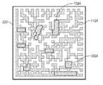
FIG. 1C shows an apparatus 50C with a third example pattern of overlaying conductive traces or closed loops 100C of an antenna on a 2D barcode 110C in accordance with an example embodiment.
In this embodiment, the conductive loops are printed without any particular regard to the location of the black ink (with the exception being the alternating black and white tiles along the top and left edges of the 2D barcode). The example shown in FIG. 1C can be read with an off-the-shelf barcode reader. Readability of the 2D barcode occurs in spite of the superimposed lines of the RFID antenna. In one embodiment, reading of the barcode in spite of the antenna loops occurs as a function of an error-code correction (ECC) algorithm, percentage of loops versus barcode area used during the production of the barcode, and the thickness of the conductive traces used for the antenna.
In FIGS. 1A-1C, the lines of the antenna and darkened areas or tiles of the barcode are printed with the same ink. Example embodiments include lines of the antenna having different lengths and widths. For example, the lines of the antenna can be approximately half the thickness of the individual modules of the barcode. As another example, the lines of the antenna can have widths of 0.25 mm, 0.5 mm, and 1.0 mm width, with laser annealing of the traces and air drying on the ink around the traces.
It should be noted that the orientation markers (the large outlining “L” of the barcodes) of the 2D barcodes can also serve as antennae that provide no interference with the readable modules.
The apparatus 50A-50C include, but are not limited to, a product such as an electronic or non-electronic device), an RFID or other tracking device that connects or attaches to a product, portable or movable devices that are sold and/or tracked. In one embodiment, the RFID antenna and barcode are affixed, deposited, and/or applied to a surface, such as a surface of the product or separate element of the apparatus that attaches to the product (e.g., a tracking device).
FIG. 2 shows a table 200 with electrical properties for different widths of antenna lines. A first column 210 shows width of traces: a second column 220 shows ohms per square on the traces; and a third column 230 shows ohms per square 250-500 micrometers from the trace.
In accordance with table 200, curing with a 405 nm laser annealing results in a 5 to 10 times conductivity difference with effective antenna traces of 500 μm or less. This corresponds to 1/50 of an inch, or 20 mils, which would allow reading from barcodes with module sizes of 40 mils or less for overwriting as described in FIG. 1C.
FIG. 3 shows an RFID chip 300 secured to a product 310 in accordance with an example embodiment. The RFID chip 300 includes an integrated circuit 320 in or on a first layer 330 and a combination RFID antenna and barcode 340 on a second layer 350. The combination RFD antenna and barcode 340 includes, but is not limited to, the embodiments shown in FIGS. 1A-1C.
FIG. 4 is a method for applying conductive ink to a surface to form loops for an antenna and a barcode.
According to block 400, electrically conductive ink is deposited on a surface of an apparatus to form a barcode.
According to block 410, the electrically conductive ink is deposited on the surface and on top of the barcode to form loops for an antenna.
In one embodiment, the loops and barcode are formed at a same time. In another embodiment, the barcodes are formed and then the loops are subsequently formed on the barcodes. In yet another embodiment, the loops are formed and then the barcode is subsequently formed on the loops.
In one embodiment, the RFID antenna and barcode are deposited on the surface in a single print operation with ink that is electrically conductive. Since the antenna and barcode are superimposed on each other and co-exist, an overall surface area for the antenna and barcode is reduced.
Example embodiments also provide flexibility in a supply chain since 2D barcodes are printed with overlying RFID antenna, while not including an ite level RFID on all units (a model for supply chain inference is discussed in connection with FIG. 5).
Example embodiments can be utilized with supply chain inference. Supply chain inference, as it applies to serialization, refers to the ability to associate unique identifiers (e.g., RFID chips) on each item in an aggregation with the aggregator (case, pallet, other shipping unit). Usually this implies a hierarchical relationship between the aggregator and each individual item.
FIG. 5 shows a supply chain inference model based on a pallet and its association with individual items in accordance with an example embodiment. A single-item pallet 500 (Item A) is defined a single item/manufacturer pallet level element (SIMPLE unit 510. The SIMPLE units multiple discrete intermediate size homogenous (DISH) units 520 and 530 which include a plurality of single items 540. A mixed pallet 550 (shown with Item A, Item C, Item D, and Item E) are divided into single-item groupings 560 (shown in one group as Items A and B; a second group as Items C, E, and F; and a third group as item D).
In FIG. 5, single-item pallets 500 are treated differently from mixed pallets 550. Many RFID-based tracking systems use a single RFID or other identifier on the pallet, regardless of how the pallet is packed. Instead of using such a single
RFID identifier, one example embodiment defines the set of all like or similar items (deemed a “single item-type grouping”) as a “SIMPLE” unit (SIMPLE=Single Item/Manufacturer Pallet-Level Element). This allows a separate inference model for all items belonging to the same class or grouping, if the other considerations (cost, regulations, feasibility, customer needs, etc.) support this grouping.
Additionally, any number of logical subdivisions of the SIMPLE units, aggregating no less than 2 single items apiece, is defined as discrete intermediate-sized homogeneous (DISH) units. Note that, in some cases (e.g. large items so that there are only several items per pallet, or low-cost items for which individual tracking is not cost-efficient), no DISH units will logically exist between the SIMPLE and single units. However, the flexibility in the SIMPLE-DISH model for inference will underpin five systems of inference described below with reference to FIG. 4 showing a SIMPLE-DISH Inference Model.
1. Inference Model
The inference model includes how tracking is performed; how items are refer or link to their parents and/or children in the supply chain; and how such associated items are associated in a registry (e.g., a database used for storing inference, tracking, authentication, forensic and other relevant data for the supply chain model).
2. Device/Data-Holder On/Off Ramp
The proposed system provides flexibility in terms of how DISH units are logically defined. For example, if the pallet contains 480 cartons of cigarettes, with 30 cartons in each of 16 boxes, and 20 packs of cigarettes in each case, each pack containing 20 cigarettes, then DISH units of the following sizes could exist
    • DISH-1: box of 30 cartons=30×20×20=12,000 single units
    • DISH-2: carton of 20 packs=20×20=400 single units
    • DISH-3: pack of 20 cigarettes=20 single units.
The overall SIMPLE unit contains 16×12,000=192,000 cigarettes in this example. The SIMPLE-DISH inference model therefore can be described as a [16, 30, 20, 20] model, meaning 20 items belong to each of 20 DISH-3 units, 20 DISH-3 units belong to each of 30 DISH-2 units, 30 DISH-2 units belong to each of 16 DISH-1 units, and the 16 DISH-1 units comprise the SIMPLE unit. The “device” or “data holder” at each level in the SIMPLE-DISH model can be chosen from RFID, printed label or other printed feature, print forensics nanotaggant, or any other reliable means of recording/reading information. This flexibility allows the supply chain manager to select device/data-holder based on the various cost factors discussed below.
3. Cost Model
The costs considered in selecting device/data-holders include the following:
a. Cost of items: How much does each level of SIMPLE and DISH unit cost versus how much the device/data-holder costs?
b. Cost of checking (visibility): How much does it cost to interrogate each device/data-holder from manufacturer to end-used (if the difference between the cost of checking is greater than the difference in device cost, then the higher-device cost, lower checking-cost should be chosen)?
c. Cost of not checking (non-visibility): What is the cost of a device/data-holder failure?
d. Cost of devices: Discussed above.
e. Cost of integration, maintenance (update, archival, etc.): Related to the cost of checking above. How much does it cost to implement any additional device/data holder systems? Additionally, consideration can be given to the relative costs of the RAD, printing and checking can be used to minimize the overall costs for a given pallet.
4. Association Model Within Like Units
How are elements within a SIMPLE or DISH unit related?
    • a. For EPC global numbers, are there differences in the variable fields related to DISH/SIMPLE units?
    • b. For fiducial-mark based data-holders (such as printed forensics, nanotaggants, etc.), are there different fiducial marks used for different units in a set?
    • c. Can different deterrents among a set of deterrents be used for each SIMPLE/DISH unit?
    • d. Is a different combination of nanotaggants usable for each of a set of SIMPLE/DISH units?
      5. Regulatory. Auditing and Compliance
How are the association models discussed above used to meet regulatory concerns, including auditing and data standards? Does this change any of the other expenses?
In each of these fives cases, the model illustrated in FIG. 5 provides a framework for comparing and contrasting overall system costs.
The methods apparatus in accordance with example embodiments are provided as examples and should not be construed to limit other embodiments within the scope of the invention. Further, methods or steps discussed within different figures can be added to or exchanged with methods of steps in other figures. Further yet, specific numerical data values (such as specific quantities, numbers, categories, etc.) or other specific information should be interpreted as illustrative for discussing example embodiments. Such specific information is not provided to limit example embodiments.
The above discussion is meant to be illustrative of the principles of various example embodiments. Numerous variations and modifications will become apparent to those skilled in the art once the above disclosure is fully appreciated. It is intended that the following claims be interpreted to embrace all such variations and modifications.

Claims (13)

What is claimed is:
1. An apparatus, comprising:
a surface that includes a two dimensional barcode and a Radio Frequency Identification (RFID) antenna printed on the two dimensional barcode, wherein the RFID antenna and the two dimensional barcode are formed from a conductive ink,
wherein every portion of the RFID antenna is formed over an ink portion of the two dimensional barcode, such that the RFID antenna is hidden within the two dimensional barcode.
2. The apparatus of claim 1, wherein the RFID antenna and the two dimensional barcode are formed from a same conductive ink.
3. The apparatus of claim 1, wherein ink that forms the RFID antenna is deposited on ink that forms the two dimensional barcode.
4. The apparatus of claim 1, wherein the RFID antenna is a closed loop that is deposited only in black ink areas of the two dimensional barcode.
5. The apparatus of claim 1, wherein the RFID antenna and the two dimensional barcode are both printed with a single pre-conductive ink that is applied in an electrically non-conductive state and then cured to an electrically conductive state.
6. A Radio Frequency Identification (RFID) device, comprising:
an antenna with a plurality of closed loops formed from a conductive ink; and
a barcode formed from the conductive ink, wherein the antenna is deposited on top of the barcode,
wherein the closed loops have a size such that one or more of:
the closed loops are ignored b a barcode reader;
a signal generated by the closed loops is corrected with error-correcting code (ECC).
7. The RFID device of claim 6, wherein the closed loops of the antenna have shapes that follow ink deposits that form the barcode.
8. The RFID device of claim 6, wherein the closed loops of the antenna and the barcode are both formed from a same transparent conductive ink that includes Indium Tin Oxide.
9. A method, comprising:
depositing an electrically conductive ink on a surface of an apparatus to form a barcode; and
depositing the electrically conductive ink on the surface and on top of the barcode to form an antenna,
wherein every portion of the antenna is deposited on an ink portion of the barcode, such that the antenna is hidden within the barcode.
10. The method of claim 9, wherein the barcode and the antenna are printed together in a single pass.
11. The method of claim 9 further comprising, curing the ink of the barcode and loops for the antenna to transform the ink from an electrically non-conductive state to an electrically conductive state.
12. The method of claim 9 further comprising, creating electrically conductive pathways for loops of the antenna on the surface where printed elements of the barcode co-exist.
13. The method of claim 9, wherein loops of the antenna have non-circular shapes that that follow a pattern created by the barcode and include an L-shape of the barcode.
US13/808,955 2010-07-09 2010-07-09 RFID antenna and 2D barcode Expired - Fee Related US9251459B2 (en)

Applications Claiming Priority (1)

Application Number Priority Date Filing Date Title
PCT/US2010/041445 WO2012005733A1 (en) 2010-07-09 2010-07-09 Rfid antenna and 2d barcode

Publications (2)

Publication Number Publication Date
US20130105587A1 US20130105587A1 (en) 2013-05-02
US9251459B2 true US9251459B2 (en) 2016-02-02

Family

ID=45441470

Family Applications (1)

Application Number Title Priority Date Filing Date
US13/808,955 Expired - Fee Related US9251459B2 (en) 2010-07-09 2010-07-09 RFID antenna and 2D barcode

Country Status (4)

Country Link
US (1) US9251459B2 (en)
CN (1) CN103098080B (en)
DE (1) DE112010005633T5 (en)
WO (1) WO2012005733A1 (en)

Cited By (6)

* Cited by examiner, † Cited by third party
Publication number Priority date Publication date Assignee Title
US20160055560A1 (en) * 2014-08-22 2016-02-25 Tofugear Limited System for facilitating point of sale transactions
US11295190B2 (en) 2016-12-14 2022-04-05 Hendrik J Volkerink Correlated asset identifier association
US11308370B2 (en) 2019-04-04 2022-04-19 Trackonomy Systems, Inc. Correlating asset identifiers
US11322971B2 (en) 2016-12-14 2022-05-03 Trackonomy Systems, Inc. Energy harvesting wireless sensing systems
US11587425B1 (en) 2020-05-17 2023-02-21 Trackonomy Systems, Inc. Next generation building access control, indoor locationing, and interaction tracking
US11907796B2 (en) 2019-11-19 2024-02-20 Trackonomy Systems, Inc. Associating assets using RFID-RF wireless gateways

Families Citing this family (8)

* Cited by examiner, † Cited by third party
Publication number Priority date Publication date Assignee Title
FR2992410A1 (en) 2012-06-26 2013-12-27 Arjowiggins Security ARTICLE COMPRISING A BAR CODE WITH ELECTROMAGNETIC SIGNATURE.
EP2736001A1 (en) * 2012-11-27 2014-05-28 Gemalto SA Electronic module with three-dimensional communication interface
US9105973B2 (en) * 2013-03-14 2015-08-11 South Dakota Board Of Regents Optically scannable code antenna
WO2016018256A1 (en) * 2014-07-29 2016-02-04 Hewlett-Packard Development Company, L.P. Display device
CL2014003255A1 (en) * 2014-11-28 2016-09-30 Tband Spa Smart tag with static and dynamic information fields.
CN104408505A (en) * 2014-12-05 2015-03-11 王若漪 Integrated type RFID two-dimension code tag
CN109196534A (en) * 2016-05-31 2019-01-11 爱克发有限公司 Authentication method for product packaging
US11481590B1 (en) * 2020-08-17 2022-10-25 Express Scripts Strategic Development, Inc. Pill bottles with conductive ink and reading systems and methods

Citations (15)

* Cited by examiner, † Cited by third party
Publication number Priority date Publication date Assignee Title
JP2000000228A (en) 1998-06-12 2000-01-07 Terumo Corp Blood specimen collection tube
US6603400B1 (en) * 2000-05-04 2003-08-05 Telxon Corporation Paper capacitor
JP2006107296A (en) * 2004-10-08 2006-04-20 Dainippon Printing Co Ltd Non-contact ic tag and antenna for non-contact ic tag
US20060186204A1 (en) * 2004-06-28 2006-08-24 International Barcode Corporation Combined multi-frequency electromagnetic and optical communication system
US20060219797A1 (en) * 2005-03-29 2006-10-05 Aruze Corp. Game card
US20070057054A1 (en) 2005-09-14 2007-03-15 Maranov John P Identification device and method
US7284704B2 (en) 2004-06-28 2007-10-23 International Barcode Corporation Combined electromagnetic and optical communication system
US20080013299A1 (en) * 2004-12-13 2008-01-17 Optomec, Inc. Direct Patterning for EMI Shielding and Interconnects Using Miniature Aerosol Jet and Aerosol Jet Array
US20080190561A1 (en) * 2007-02-14 2008-08-14 Norimitsu Sanbongi Apparatus and method for producing a sheet material
US20090039162A1 (en) * 2007-08-10 2009-02-12 Leeway Yen Tag reader and the tag
US20100090008A1 (en) 2008-10-13 2010-04-15 Oded Bashan Authentication seal
US20110017834A1 (en) * 2007-12-22 2011-01-27 Detlef Schulze-Hagenest Method for producing an antenna structure for an rfid device, and dry toner for use in producing such antenna structure
US20110062237A1 (en) * 2009-09-17 2011-03-17 Sap Ag Integrated smart label
US8096479B2 (en) * 2007-02-23 2012-01-17 Newpage Wisconsin System Inc. Multifunctional paper identification label
US20120140333A1 (en) * 2010-12-07 2012-06-07 John Tomczyk Lens sheet having lens array formed in pre-selected areas and articles formed therefrom

Family Cites Families (2)

* Cited by examiner, † Cited by third party
Publication number Priority date Publication date Assignee Title
JP2000090228A (en) * 1998-09-09 2000-03-31 Sony Corp Information storage medium
CN106376174B (en) * 2008-02-05 2019-06-07 普林斯顿大学理事会 Electronic device and the method for forming electronic device

Patent Citations (17)

* Cited by examiner, † Cited by third party
Publication number Priority date Publication date Assignee Title
JP2000000228A (en) 1998-06-12 2000-01-07 Terumo Corp Blood specimen collection tube
US6603400B1 (en) * 2000-05-04 2003-08-05 Telxon Corporation Paper capacitor
US20060186204A1 (en) * 2004-06-28 2006-08-24 International Barcode Corporation Combined multi-frequency electromagnetic and optical communication system
US7284704B2 (en) 2004-06-28 2007-10-23 International Barcode Corporation Combined electromagnetic and optical communication system
JP2006107296A (en) * 2004-10-08 2006-04-20 Dainippon Printing Co Ltd Non-contact ic tag and antenna for non-contact ic tag
US20080013299A1 (en) * 2004-12-13 2008-01-17 Optomec, Inc. Direct Patterning for EMI Shielding and Interconnects Using Miniature Aerosol Jet and Aerosol Jet Array
US20060219797A1 (en) * 2005-03-29 2006-10-05 Aruze Corp. Game card
US7546948B2 (en) 2005-09-14 2009-06-16 Meadwestvaco Corporation Identification device and method
US20070057054A1 (en) 2005-09-14 2007-03-15 Maranov John P Identification device and method
CN101479740A (en) 2006-04-03 2009-07-08 国际条形码公司 Combined multi-frequency electromagnetic and optical communication system
US20080190561A1 (en) * 2007-02-14 2008-08-14 Norimitsu Sanbongi Apparatus and method for producing a sheet material
US8096479B2 (en) * 2007-02-23 2012-01-17 Newpage Wisconsin System Inc. Multifunctional paper identification label
US20090039162A1 (en) * 2007-08-10 2009-02-12 Leeway Yen Tag reader and the tag
US20110017834A1 (en) * 2007-12-22 2011-01-27 Detlef Schulze-Hagenest Method for producing an antenna structure for an rfid device, and dry toner for use in producing such antenna structure
US20100090008A1 (en) 2008-10-13 2010-04-15 Oded Bashan Authentication seal
US20110062237A1 (en) * 2009-09-17 2011-03-17 Sap Ag Integrated smart label
US20120140333A1 (en) * 2010-12-07 2012-06-07 John Tomczyk Lens sheet having lens array formed in pre-selected areas and articles formed therefrom

Non-Patent Citations (2)

* Cited by examiner, † Cited by third party
Title
International Search Report and Written Opinion issued in internation Application No. PCT/US2010/041445 (mailed Mar. 29, 2011).
People Republic China IPO Search Report, issued Mar. 31, 2015, in related China application 201080069039.9.

Cited By (8)

* Cited by examiner, † Cited by third party
Publication number Priority date Publication date Assignee Title
US20160055560A1 (en) * 2014-08-22 2016-02-25 Tofugear Limited System for facilitating point of sale transactions
US11295190B2 (en) 2016-12-14 2022-04-05 Hendrik J Volkerink Correlated asset identifier association
US11322971B2 (en) 2016-12-14 2022-05-03 Trackonomy Systems, Inc. Energy harvesting wireless sensing systems
US11843276B2 (en) 2016-12-14 2023-12-12 Trackonomy Systems, Inc. Energy harvesting wireless sensing systems
US11308370B2 (en) 2019-04-04 2022-04-19 Trackonomy Systems, Inc. Correlating asset identifiers
US11816514B2 (en) 2019-04-04 2023-11-14 Trackonomy Systems, Inc. Correlating asset identifiers
US11907796B2 (en) 2019-11-19 2024-02-20 Trackonomy Systems, Inc. Associating assets using RFID-RF wireless gateways
US11587425B1 (en) 2020-05-17 2023-02-21 Trackonomy Systems, Inc. Next generation building access control, indoor locationing, and interaction tracking

Also Published As

Publication number Publication date
CN103098080B (en) 2016-11-02
CN103098080A (en) 2013-05-08
WO2012005733A1 (en) 2012-01-12
DE112010005633T5 (en) 2013-03-28
US20130105587A1 (en) 2013-05-02

Similar Documents

Publication Publication Date Title
US9251459B2 (en) RFID antenna and 2D barcode
EP1756759B1 (en) Item carrying at least two data storage elements
US8292178B2 (en) Integrated smart label
US20080272885A1 (en) Modular Radio Frequency Identification Tagging Method
Nilsson et al. System integration of electronic functions in smart packaging applications
JP2006107296A (en) Non-contact ic tag and antenna for non-contact ic tag
TW200926006A (en) Method for the manufacture of a laser-inscribable and adhesive smart label
EP3500973B1 (en) Providing and reading a marking on an item
US20130221108A1 (en) Optically-readable electromagnetic antenna
TWI713554B (en) Color sample device and method for producing the same, a corresponding data processing apparatus, a system, and a data storage medium, and a use thereof
KR100682590B1 (en) ISO card combined with RFID card tag get rid of frequency interference
US20110140860A1 (en) Heat transfer printing electronic radio frequency identification tag
CN110443336A (en) RFID tamper-evident anti-metal electronic tag
US20240054313A1 (en) Multi-purpose rfid label
US10311269B2 (en) Method and system for improving the reading efficiency of RFID tags
JP2017112449A (en) Metal compatible chipless rfid tag and information carrier
JP5311022B2 (en) Optically variable device with IC tag inlet
OA18933A (en) Providing and reading a marking on an item.
SI24272A (en) Packaging made of paperboard with an installed smart tag for radio-frequency identification with the possibility of recording different parameters
WO2011004070A1 (en) Device for identifying an object
WO2014021857A1 (en) Electronic shutter over image to render image optically readable or unreadable
JP2009116710A (en) Inlet for noncontact ic tag, noncontact ic tag, and manufacturing method therefor
JP2012230477A (en) Electronic tag for discoid recording medium

Legal Events

Date Code Title Description
AS Assignment

Owner name: HEWLETT-PACKARD DEVELOPMENT COMPANY, L.P., TEXAS

Free format text: ASSIGNMENT OF ASSIGNORS INTEREST;ASSIGNORS:SIMSKE, STEVEN J;ARONOFF, JASON S;GORE, MAKARAND P;AND OTHERS;SIGNING DATES FROM 20100621 TO 20100630;REEL/FRAME:029617/0505

ZAAA Notice of allowance and fees due

Free format text: ORIGINAL CODE: NOA

ZAAB Notice of allowance mailed

Free format text: ORIGINAL CODE: MN/=.

ZAAA Notice of allowance and fees due

Free format text: ORIGINAL CODE: NOA

ZAAB Notice of allowance mailed

Free format text: ORIGINAL CODE: MN/=.

STCF Information on status: patent grant

Free format text: PATENTED CASE

CC Certificate of correction
MAFP Maintenance fee payment

Free format text: PAYMENT OF MAINTENANCE FEE, 4TH YEAR, LARGE ENTITY (ORIGINAL EVENT CODE: M1551); ENTITY STATUS OF PATENT OWNER: LARGE ENTITY

Year of fee payment: 4

FEPP Fee payment procedure

Free format text: MAINTENANCE FEE REMINDER MAILED (ORIGINAL EVENT CODE: REM.); ENTITY STATUS OF PATENT OWNER: LARGE ENTITY

LAPS Lapse for failure to pay maintenance fees

Free format text: PATENT EXPIRED FOR FAILURE TO PAY MAINTENANCE FEES (ORIGINAL EVENT CODE: EXP.); ENTITY STATUS OF PATENT OWNER: LARGE ENTITY

STCH Information on status: patent discontinuation

Free format text: PATENT EXPIRED DUE TO NONPAYMENT OF MAINTENANCE FEES UNDER 37 CFR 1.362

FP Lapsed due to failure to pay maintenance fee

Effective date: 20240202