US9236800B2 - System for balancing current supplied to a load - Google Patents
System for balancing current supplied to a load Download PDFInfo
- Publication number
- US9236800B2 US9236800B2 US14/068,721 US201314068721A US9236800B2 US 9236800 B2 US9236800 B2 US 9236800B2 US 201314068721 A US201314068721 A US 201314068721A US 9236800 B2 US9236800 B2 US 9236800B2
- Authority
- US
- United States
- Prior art keywords
- current
- regulator
- load
- regulators
- operable
- Prior art date
- Legal status (The legal status is an assumption and is not a legal conclusion. Google has not performed a legal analysis and makes no representation as to the accuracy of the status listed.)
- Active
Links
Images


Classifications
-
- H—ELECTRICITY
- H02—GENERATION; CONVERSION OR DISTRIBUTION OF ELECTRIC POWER
- H02M—APPARATUS FOR CONVERSION BETWEEN AC AND AC, BETWEEN AC AND DC, OR BETWEEN DC AND DC, AND FOR USE WITH MAINS OR SIMILAR POWER SUPPLY SYSTEMS; CONVERSION OF DC OR AC INPUT POWER INTO SURGE OUTPUT POWER; CONTROL OR REGULATION THEREOF
- H02M3/00—Conversion of dc power input into dc power output
- H02M3/02—Conversion of dc power input into dc power output without intermediate conversion into ac
- H02M3/04—Conversion of dc power input into dc power output without intermediate conversion into ac by static converters
- H02M3/10—Conversion of dc power input into dc power output without intermediate conversion into ac by static converters using discharge tubes with control electrode or semiconductor devices with control electrode
- H02M3/145—Conversion of dc power input into dc power output without intermediate conversion into ac by static converters using discharge tubes with control electrode or semiconductor devices with control electrode using devices of a triode or transistor type requiring continuous application of a control signal
- H02M3/155—Conversion of dc power input into dc power output without intermediate conversion into ac by static converters using discharge tubes with control electrode or semiconductor devices with control electrode using devices of a triode or transistor type requiring continuous application of a control signal using semiconductor devices only
- H02M3/156—Conversion of dc power input into dc power output without intermediate conversion into ac by static converters using discharge tubes with control electrode or semiconductor devices with control electrode using devices of a triode or transistor type requiring continuous application of a control signal using semiconductor devices only with automatic control of output voltage or current, e.g. switching regulators
- H02M3/158—Conversion of dc power input into dc power output without intermediate conversion into ac by static converters using discharge tubes with control electrode or semiconductor devices with control electrode using devices of a triode or transistor type requiring continuous application of a control signal using semiconductor devices only with automatic control of output voltage or current, e.g. switching regulators including plural semiconductor devices as final control devices for a single load
-
- H—ELECTRICITY
- H02—GENERATION; CONVERSION OR DISTRIBUTION OF ELECTRIC POWER
- H02M—APPARATUS FOR CONVERSION BETWEEN AC AND AC, BETWEEN AC AND DC, OR BETWEEN DC AND DC, AND FOR USE WITH MAINS OR SIMILAR POWER SUPPLY SYSTEMS; CONVERSION OF DC OR AC INPUT POWER INTO SURGE OUTPUT POWER; CONTROL OR REGULATION THEREOF
- H02M3/00—Conversion of dc power input into dc power output
- H02M3/02—Conversion of dc power input into dc power output without intermediate conversion into ac
- H02M3/04—Conversion of dc power input into dc power output without intermediate conversion into ac by static converters
- H02M3/10—Conversion of dc power input into dc power output without intermediate conversion into ac by static converters using discharge tubes with control electrode or semiconductor devices with control electrode
- H02M3/145—Conversion of dc power input into dc power output without intermediate conversion into ac by static converters using discharge tubes with control electrode or semiconductor devices with control electrode using devices of a triode or transistor type requiring continuous application of a control signal
- H02M3/155—Conversion of dc power input into dc power output without intermediate conversion into ac by static converters using discharge tubes with control electrode or semiconductor devices with control electrode using devices of a triode or transistor type requiring continuous application of a control signal using semiconductor devices only
- H02M3/156—Conversion of dc power input into dc power output without intermediate conversion into ac by static converters using discharge tubes with control electrode or semiconductor devices with control electrode using devices of a triode or transistor type requiring continuous application of a control signal using semiconductor devices only with automatic control of output voltage or current, e.g. switching regulators
- H02M3/157—Conversion of dc power input into dc power output without intermediate conversion into ac by static converters using discharge tubes with control electrode or semiconductor devices with control electrode using devices of a triode or transistor type requiring continuous application of a control signal using semiconductor devices only with automatic control of output voltage or current, e.g. switching regulators with digital control
-
- H—ELECTRICITY
- H02—GENERATION; CONVERSION OR DISTRIBUTION OF ELECTRIC POWER
- H02M—APPARATUS FOR CONVERSION BETWEEN AC AND AC, BETWEEN AC AND DC, OR BETWEEN DC AND DC, AND FOR USE WITH MAINS OR SIMILAR POWER SUPPLY SYSTEMS; CONVERSION OF DC OR AC INPUT POWER INTO SURGE OUTPUT POWER; CONTROL OR REGULATION THEREOF
- H02M3/00—Conversion of dc power input into dc power output
- H02M3/02—Conversion of dc power input into dc power output without intermediate conversion into ac
- H02M3/04—Conversion of dc power input into dc power output without intermediate conversion into ac by static converters
- H02M3/10—Conversion of dc power input into dc power output without intermediate conversion into ac by static converters using discharge tubes with control electrode or semiconductor devices with control electrode
- H02M3/145—Conversion of dc power input into dc power output without intermediate conversion into ac by static converters using discharge tubes with control electrode or semiconductor devices with control electrode using devices of a triode or transistor type requiring continuous application of a control signal
- H02M3/155—Conversion of dc power input into dc power output without intermediate conversion into ac by static converters using discharge tubes with control electrode or semiconductor devices with control electrode using devices of a triode or transistor type requiring continuous application of a control signal using semiconductor devices only
- H02M3/156—Conversion of dc power input into dc power output without intermediate conversion into ac by static converters using discharge tubes with control electrode or semiconductor devices with control electrode using devices of a triode or transistor type requiring continuous application of a control signal using semiconductor devices only with automatic control of output voltage or current, e.g. switching regulators
- H02M3/158—Conversion of dc power input into dc power output without intermediate conversion into ac by static converters using discharge tubes with control electrode or semiconductor devices with control electrode using devices of a triode or transistor type requiring continuous application of a control signal using semiconductor devices only with automatic control of output voltage or current, e.g. switching regulators including plural semiconductor devices as final control devices for a single load
- H02M3/1584—Conversion of dc power input into dc power output without intermediate conversion into ac by static converters using discharge tubes with control electrode or semiconductor devices with control electrode using devices of a triode or transistor type requiring continuous application of a control signal using semiconductor devices only with automatic control of output voltage or current, e.g. switching regulators including plural semiconductor devices as final control devices for a single load with a plurality of power processing stages connected in parallel
-
- Y10T307/565—
Definitions
- the present application generally relates to providing regulated power to a load and more particularly to balancing current provided by multiple power regulators.
- Power regulation for a microelectronic device such as a microprocessor must include a steady voltage along a predetermined load line and an ability to respond to dynamic current demands of the processor. For example, as a microprocessor executes instructions, particularly at faster rates, severe power transients and widely varying current requirements are likely to occur. Buck converters have been advantageously utilized to meet the power demands of microprocessors; which typically require very high currents at very low voltages.
- a regulator located at or near the load can improve the precision of regulated power provided to the load.
- Point of load (POL) regulators are well known.
- various power regulators have been disclosed. However, in some applications, more than one regulator is required because one regulator cannot provide the large amount of current required either as a steady-state or as a transient response.
- a problem with utilizing multiple regulators is the inefficiency that occurs when various regulators provide different levels of current to the load.
- the method includes: measuring an average load current supplied by each regulator; determining an overall average current to be shared by the plurality of regulators; comparing each average load current with the overall average current to be shared by the plurality of regulators; and adjusting an output current of one or more of the plurality of regulators so that the plurality of regulators supply the same current to the load.
- the method includes: supplying current to the load during a first phase via a first regulator; supplying current to the load during a second phase via a second regulator; determining a first average current provided to the load during the first phase and a second average current provided to the load during the second phase; determining an overall average current to be shared by the first and second regulators; comparing the first average current provided to the load during the first phase with the overall average current to be shared by the first and second regulators; and comparing the second average current provided to the load during the second phase with the overall average current to be shared by the first and second regulators.
- the method includes: coupling a first regulator to the load; coupling a second regulator to the load; and balancing a current provided by the first regulator to the load and a current provided by the second regulator to the load based on a comparison of an overall average current value with the current provided by each regulator.
- FIG. 1 is a block diagram of a regulator circuit incorporating a power supply balancing circuit in accordance with an embodiment.
- FIG. 2 is a simplified block diagram illustrating a current balancing circuit with 2 regulators in a 2 phase system.
- FIG. 3 is a block diagram illustrating current sharing in accordance with an embodiment.
- FIG. 4 is a waveform diagram illustrating the operation of an embodiment of a current sharing feature.
- FIG. 5 is a block diagram illustrating an exemplary digital embodiment.
- FIG. 6A is a block diagram illustrating an exemplary embodiment of a digital implementation of current sharing in four phases.
- FIG. 6B is a block diagram illustrating an exemplary embodiment of an analog implementation of current sharing in four phases.
- FIG. 7 is a waveform diagram illustrating the operation of the four phase embodiment illustrated in FIG. 6A .
- FIG. 8 is a flow chart illustrating an exemplary embodiment of a method of operation.
- FIGS. 9-10 illustrate circuits for sensing load current.
- FIG. 11 is a simplified illustration of an embodiment.
- FIG. 1 for a block diagram illustrating a switched power converter, i.e. regulator, incorporating the current sharing circuit 100 in accordance with an embodiment.
- the regulator 10 (without the current sharing circuit 100 ) has previously been described in detail, for example, in the cross-referenced patent applications that have been incorporated herein by reference.
- This type of regulator is also known as a Buck Converter or Multiphase Buck Converter and it converts a relatively high supply potential (+V) at e.g. 12 volts to a low voltage, e.g. 1 to 3 volts that is provided at very high current levels to a load.
- Regulator 10 is shown including Single or Multi-phase Pulse Width Modulator (PWM) 20 .
- PWM Pulse Width Modulator
- the output of PWM 20 is a series of pulses on each of its output lines, a first phase output being provided to the driver in power stage 30 and a second phase output being provided to the driver circuit in power stage 30 ′.
- additional phases are connected in a similar manner.
- Low side FETs 50 and 52 , inductors 60 and 62 , and capacitor 70 are typically discrete devices.
- a pulse output stage comprises a high side FET ( 40 ), a low side FET ( 50 ) and an inductor ( 60 ).
- the pulse output stage for the second phase comprises a high side FET 42 , a low side FET 52 and an inductor 62 .
- the pulse output stage charges up capacitor 70 and supplies power to the load.
- Load 80 is typically a microelectronic component, such as a microprocessor, requiring very accurate power that is regulated and maintained during rapidly changing power requirements.
- Current sensor 11 senses the current at nodes A and B. This is the current supplied to load 80 .
- the output of the current sensor 11 , as well as the load voltage are provided to multiplex circuit 13 .
- Multiplex circuit 13 provides these values to analog to digital converter (ADC) 16 at the time when the phase desired to be measured is active.
- ADC 16 also receives an input from voltage reference 14 .
- the reference voltage from block 14 is used to calibrate the output of ADC 16 to that reference voltage.
- a VID input is received at voltage control 12 .
- VID is a digital number provided by the microprocessor manufacturer describing specific power requirements.
- Analog-digital converter 16 also receives, as another input, the voltage at load 80 coupled through multiplex circuit 13 .
- the output of ADC 16 is a digital voltage value that is de-multiplexed through de-multiplex circuit 19 to current share circuit 100 (via conductor 104 ) and digital compensator 18 .
- the output of ADC 16 is also compared to the output of voltage control circuit 12 (the target voltage) in summer 17 and provided as a digital error voltage to digital compensator 18 .
- digital compensator 18 then provides an input to PWM 20 in order to modify the width of the pulses provided to the drivers in power stages 30 and 30 ′, etc. of each of the two phases in the illustrated example, and other phases, when utilized.
- current share circuit 100 provides an output to digital compensator 18 on conductor 106 to further modify (increase or decrease, as the case may be) the width of the pulses provided to the drivers in power stages 30 and 30 ′, etc.
- the output of regulator 10 will provide the same current to load 80 as the other regulators that are also coupled to load 80 .
- the first phase is driven by driver circuits 32 and 34 .
- Circuit 32 drives the gate of FET 40 with a signal that is complementary to the output of circuit 34 that drives the gate of FET 50 .
- FET 40 and 50 have their drain-source paths connected in series, at a common point A, between a first potential source (+V) and a second potential source (ground). Since both FET 40 and 50 are shown as N-channel devices, only one of the two transistors is on at any one time. Of course, if transistor 40 were to be replaced with a P-type transistor, then the same phase signal could be used to drive the gate of both transistor 40 and 50 . In either case, there is never a direct current path between +V and ground.
- the second phase output of PWM 20 is provided to driver circuits 36 and 38 during the second phase in the same way that circuits 32 and 34 receive the pulse width modulated signals during the first phase.
- Circuit 36 then drives the gate of FET 42 and circuit 38 drives the gate of FET 52 .
- any number of phases can be used. Larger number of phases can provide higher current levels and also smoother and more accurately regulated power to the load.
- regulator 10 further improvement is provided by the addition of additional regulators such as regulator 10 , as described herein. Then, assuming that one regulator (such as regulator 10 ) can deliver 30 Amps, then 4 power regulators can deliver 120 Amps. In order to achieve optimum efficiency, the total current provided to the load should be shared equally by all regulators.
- current share circuit 100 is coupled to similar current share circuits in the other plurality of power regulators by terminals 101 and 102 .
- terminal 101 is a terminal for Ishare_in to current share circuit 100
- terminal 102 is a terminal for Ishare_out.
- the coupling of one or more additional power regulators to regulator 10 is achieved by the coupling of the respective terminals 101 and 102 to current share circuits in the additional power regulators.
- FIG. 2 illustrates current sharing with 2 regulators. This is the case where a load 80 is supplied by two regulators, such as regulator 10 in FIG. 1 .
- the circuit of FIG. 2 illustrates two current share circuits, one in each of two regulators.
- current share circuit 100 is a more detailed illustration of current share circuit 100 within the regulator 10 of FIG. 1 ; while current share circuit 252 is a similar circuit within a second regulator coupled to the regulator 10 of FIG. 1 .
- Circuit 100 receives the digitized value of the average current sensed at the load during the time that regulator 1 is active (phase 1 time) at terminal (conductor) 104 .
- DAC 206 This value is received into N Bit Digital to Analog Converter (DAC) 206 .
- DAC 206 can conveniently be a 6 bit DAC or the like.
- the analog current value received at node 208 is the first phase current (current sensed when regulator 10 is active) and is supplied as a first input to comparator 210 .
- Resistor R 1 couples node 208 to node 212 and external capacitor C 1 which has its other capacitor lead coupled to ground potential.
- Node 212 is coupled to the second input of comparator 210 by conductor 214 .
- the output of comparator 210 is coupled to the input of filter 216 ; which provides an output that will appropriately adjust the current output of the regulator, e.g. regulator 10 .
- node 212 is coupled to terminal 101 while ground sense node 213 is coupled to terminal 102 .
- Circuit 252 receives the digitized value of the average current sensed at the load during the time that regulator 2 is active (phase 2 time), at terminal 254 . This value is received into N Bit Digital to Analog Converter (DAC) 256 .
- DAC 256 can conveniently be a 6 bit DAC or the like.
- the analog current value received at node 256 is the second phase current and is supplied as a first input to comparator 260 .
- Resistor R 2 couples node 258 to node 212 and external capacitor C 1 which has its other capacitor lead coupled to ground potential.
- Node 212 is coupled to the second input of comparator 260 by conductor 264 .
- the output of comparator 260 is coupled to the input of filter 266 ; which provides an output that will appropriately adjust the current output of the second regulator.
- external capacitor C 1 generates a voltage that is proportional to the average currents of regulator 1 and regulator 2 . That is, at node 212 , the first average (regulator 1 ) current and the second average (regulator 2 ) current are added and then divided by 2 to represent the overall average current sensed at the load. This overall average current (represented by a voltage) is referenced to ground sense 213 (for regulator 100 ) and 213 ′ (for regulator 252 ). Nodes 213 and 213 ′ are connected in a star configuration (node S) at capacitor C 1 , thereby preventing variations in the local ground voltage levels from affecting the accuracy of the average current determination.
- comparators 210 and 260 This overall average current value (from summing node 212 ) is provided to comparators 210 and 260 .
- the respective comparators then provide either an up or down output to indicate that the corresponding regulator should provide more or less current to achieve the average.
- comparators 210 and 260 are provided with a hysteresis feature as will be described in greater detail below.
- Least Significant Bit (LSB) Modulator 218 is shown coupled between terminal 204 and 6 Bit DAC 206 .
- LSB Modulator 218 is a “digital rounding device” and can be of a construction known in the art. For example, it can be a Sigma Delta converter that looks at the number of binary 1's and 0's received over a period of time and then provides a signal to reduce the output voltage or current of the power source.
- LSB Modulator 218 rounds this digital number to 6 bits. In its most accurate form, LSB Modulator 218 tracks the value of the four least significant bits to assure that the six bits inputted into 6 bit DAC 206 accurately define the measured current value.
- the LSB Modulator 218 , DAC 206 , Integrator 216 and Comparator 210 receive the same clock signal to operate synchronously.
- DAC 206 also receives an “Enable” signal to gate the output during a desired portion of the first phase.
- Integrator 216 is a filter that integrates a number of Up/Down signals from Comparator 210 before sending a signal, for example, to reduce the current output of the current source associated with the first phase.
- comparator 210 is effectively an analog to digital converter in the sense that after comparing the level of the two analog input signals it provides a binary up or binary down number to integrator 216 .
- Resistor R 3 and current source 220 are coupled in a series path between node 208 and a potential level such as ground. These form a biasing circuit to the input of comparator 210 coupled to R 3 resulting in a hysteresis effect.
- the signal provided as an input to comparator 210 can be varied from the actual phase one voltage at node 208 .
- comparator 210 can provide a down number output only after the phase one voltage exceeds the average voltage received on conductor 214 by “delta V”, a value determined by the programmed level applied to current source 220 in combination with the value of resistor R 3 .
- Capacitors C 2 and C 3 are filter capacitors used in their known manner.
- the added elements on the second regulator side of the FIG. 3 illustration are the same as for first phase and perform the same functions.
- the clock signals coupled to DAC 256 , LSB Modulator 268 , Comparator 260 and Integrator 266 , as well as the Enable signal coupled to DAC 256 are for the second phase.
- the programmable bias set by current source 250 and resistor R 4 are usually set at the same level as for the regulator 1 circuit.
- Capacitors C 4 and C 5 are of the same values as C 2 and C 3 .
- the hysteresis function can be best understood by referring to FIG. 4 as well as continued reference to FIG. 3 .
- V 1 and V 2 At the intersection of voltage V 1 and V 2 , at point A, both power sources are providing the same average voltage “V average”. This is the ideal situation.
- V 1 increases to exceed delta V (point B)
- V 2 increases to exceed delta V (point C)
- a correction signal to reduce the output voltage of the power stage for regulator 2 is provided by integrator 266 .
- no correction signal is provided.
- V 1 is the voltage at node 208 and is equal to the current detected at the load during the first phase times a constant.
- Delta V is the voltage drop across resistor R 3 as determined by the value of R 3 times the amplitude of the programmable current drawn by current source 220 .
- the input voltage applied to comparator 210 is V 1 minus delta V.
- the input voltage applied to comparator 260 is V 2 (the voltage at node 258 as determined during the second phase) minus delta V (as determined by the value of R 4 times the amplitude of the programmable current drawn by current source 250 ). Note the dead zone in FIG. 4 where no correction is provided.
- FIG. 5 is a block diagram of a current share regulator for one regulator that is entirely digital.
- the digital representation of the load current measured during the time the illustrated regulator is active is received at terminal 304 (connected for example to conductor 104 in FIG. 1 ) and is inputted to digital divider 306 and digital comparator 310 .
- digital divider 306 the digital representation of load current is divided by an arbitrarily selected constant N, which can be equal to 64. This weighted value of current is provided to summer 308 .
- the output of summer 308 is provided as a second input to comparator 310 on conductor 314 .
- the output of comparator 310 is provided to integrator 316 .
- Integrator 316 also receives a clock signal, as is well known for such devices.
- the output of integrator 316 is coupled to the digital compensator 18 ( FIG. 1 ) (via conductor 106 , for example) and is a signal to reduce the output of the regulator when the digital comparator 310 has provided an output indicating that the output of the regulator is greater than the shared average current value by more than the hysteresis amount delta V, as illustrated in FIG. 4 .
- the illustrated regulator is typically connected to other regulators. Each such regulator is active during its assigned time slot (phase).
- the previous regulator provides an Iin_Share input on terminal 320 .
- An Iout_Share output is provided to the next regulator on output terminal 322 . (These correspond, for example to terminals 101 and 102 in FIG. 1 .)
- the signal on the input terminal 320 is a serial digital bit stream representing the average shared current and is inputted into serial to parallel converter 324 .
- Serial to parallel converters are well-known, as for example shift registers that receive digital information in series at a first clock frequency and output the digital information in parallel at a second (slower) clock frequency.
- the average current value is provided to digital multiplier circuit 326 .
- This weighted current value is provided as a second input to summing circuit 308 .
- the output of summer 308 on conductive line 314 will be equal to the value on terminal 304 .
- This current value is inputted to parallel to serial converter 328 where it is converted into a serial bit stream and provided to the next phase on terminal 322 , as will be more clearly understood by reference to FIG. 6A .
- the embodiments described herein can be adapted to control N regulators operated during N phases.
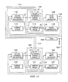
- FIG. 6A for an example of a four phase configuration to illustrate how four regulators (operating in the digital mode as illustrated for example in FIG. 5 ) would be connected.
- Each of these 4 regulators receives the same frequency clock input (not shown) and is therefore frequency coherent.
- the phase occurrence of when a particular regulator is enabled is arbitrary.
- the concept is the same as in the previously described two phase embodiments in that the shared current I share is desired to be the same in all power stages.
- the connection shown in FIG. 6A is known as a daisy chain and would be used with digital current share circuits as illustrated in FIG. 5 .
- the digital representation of the shared current (Ishare_in) is inputted into Regulator #1 (via conductor 320 ) from where it is outputted (as Ishare_out) (via conductor 322 ) into Regulator #2.
- the output of Regulator #2 is inputted to Regulator #3.
- the output of Regulator #3 is inputted into Regulator #4.
- the output of Regulator #4 is the shared current inputted into Regulator #1.
- the load 80 has been identified with the same reference numeral as in the FIG. 1 illustration.
- FIG. 6B is an example of a four regulator, i.e. four phase configuration to illustrate how four regulators (operating in the analog mode as illustrated for example in the FIG. 3 two regulator example) would be connected.
- Capacitor C 1 and load 80 have been identified as in previous drawing figures.
- all the Ishare_in terminals (corresponding to terminal 101 in FIG. 1 ) are coupled in common and to node 212 ( FIG. 3 ).
- All the Ishare_out terminals (corresponding to terminal 102 in FIG. 1 ) are coupled in common and to a commoned ground connection (e.g. 213 and 213 ′ in FIG. 3 ).
- FIG. 7 illustrates the convergence of the average current ring.
- regulator 1 i.e. the first phase
- regulator 2 i.e. the second phase
- current I 2 20 Amps
- Regulator 3 i.e. phase 3
- current I 3 24 Amps
- N 64 (average weighting).
- N determines the gain or convergence rate, i.e. error v. number of samples.
- the average current I average daisy chain converges to the average of the 4 regulators in approximately 100 cycles (i.e. 100 samples).
- FIG. 8 is a flow chart illustrating an embodiment. As shown, we measure the average load current during the active phase of each regulator. These measurements can be taken in a number of ways previously described in the above referenced patent application, entitled: DIGITAL CALIBRATION WITH LOSSLESS SENSING IN A MULTIPHASE SWITCHED POWER CONVERTER, that described various lossless current measuring techniques. The measurement can then be digitized and processed digitally, as illustrated in FIG. 5 , or converted to an analog value, as in FIGS. 2 and 3 . All subsequent steps can be performed either digitally or by analog techniques. We then determine the average current to be shared by the regulators.
- the average current to be shared by the regulated power supplies can be achieved by an iterative process, as shown in FIG. 7 , with a daisy chain as illustrated in FIG. 6A .
- the dashed line in FIG. 8 represents the iterative process.
- the embodiments described herein utilize the accurate and relatively lossless sensing of load current. These measurements can be taken, for example at nodes A and B ( FIG. 1 ). Unfortunately, voltage measurements taken at nodes A and B are only an approximation of current. The voltage measurement taken at node B for example, when low side FET is in its conductive state is the product of the current and on resistance (also referred to as RDSON) of low side FET 52 . Because of process variations in the fabrication of FET 52 and other field effect transistors on the semiconductor chip and the fact that conductance is a function of temperature, measurements taken at nodes A and B, etc. are not a truly accurate measurement of current, unless actual RDSON is known. To overcome this problem actual RDSON can be determined as disclosed in the above referenced patent application entitled: DIGITAL CALIBRATION WITH LOSSLESS SENSING IN A MULTIPHASE SWITCHED POWER CONVERTER.
- FIG. 9 illustrates a lossless technique for measuring load current utilizing a current mirror and precision resistor placed in parallel with the high side FET.
- FIG. 9 is similar to FIG. 1 and to the extent possible, corresponding elements have been numbered with corresponding reference numerals. However, since the FIG. 9 embodiment is a four phase example, additional high side FETs 44 , 46 , additional low side FETs 54 , 56 , and additional inductors 64 , 66 have been added.
- block 501 includes, in addition to high side FET 40 , a current mirror with a 1:N ratio.
- a current that is a known ratio of the high side FET current can be measured by measuring the voltage across current mirror resistor (Rmirror) 511 ; which has a known precise value.
- blocks 502 , 503 , 504 include a current mirror in addition to the high side FET.
- the current in the second, third and fourth phases is measured across precision current mirror resistors 512 , 513 , and 514 , respectively.
- the current passing through the current mirror will track the load current with temperature.
- the high side FET is typically conducting for a much shorter period than the low side FET and therefore represents the load current for a shorter period of time.
- the extra chip area used by the current mirrors and the need for precision resistors can increase the cost of sensing current with this embodiment.
- the power consumed by the current mirror is negligible so that the current is sensed essentially in a lossless manner.
- calibration can compensate for various process induced differences in the components. For example, variations in the actual ratio of the current mirror current to the current passing through the high side FET can be compensated. As in other embodiments, variations in the response of sense amplifiers 130 , 140 , 150 and 160 can be compensated. For example, when the low side FETs are on, the corresponding high side FETs are off and the resultant sense amplifier output should indicate zero current. To the extent a sense amplifier provides a current that is not zero, this is a known error that can be compensated by subtracting out the error in the measured current.
- FIG. 10 for a still further embodiment, sensing current through the direct current resistance (DCR) of an inductor.
- DCR direct current resistance
- FIG. 10 illustrates a four phase system. Corresponding elements have again been numbered with corresponding numerals. In each phase, a resistor and capacitor have been added in parallel with the inductor. Thus phases 1-4 have resistors 90 , 91 , 92 , and 93 and capacitors 94 , 95 , 96 , and 97 , respectively connected in series in each stage and in parallel with the inductor in that phase, all as shown.
- the DC resistive component is separately shown for each of the inductors as RDCR. It is known that all inductors have inherent DC resistors.
- inductors with relatively high DC resistance with known resistor values are selected. This permits accurate current measurement in a Wheatstone Bridge like arrangement.
- the AC component of the voltage is filtered out and the voltage across the capacitors 94 , 95 , 96 , and 97 is the same as the voltage across the corresponding RDCR resistor. Therefore, a voltage measurement across these capacitors provides the actual current simply by dividing the voltage by the known resistance. The processing of this precisely known current is then accomplished in the same manner as previously described.
- FIG. 11 shows two regulators, such as regulator 10 ( FIG. 1 ).
- a first regulator has an output line 1102 coupled to load 1300 for supplying current to load 1300 during a first phase.
- a second regulator usually of the same construction as the first regulator, has an output line 1202 coupled to load 1300 .
- a first current share circuit 1104 is coupled to the load for measuring and comparing the current provided to the load 1300 during the first phase.
- current share circuit 1104 comprises the circuitry illustrated in FIG. 5 .
- current share circuit 1104 comprises the circuitry illustrated in FIGS. 2 and 3 , including capacitor C 1 and the summing node 212 .
- the load voltage is coupled to voltage reference and control circuit 1106 .
- Voltage reference and control circuit 1106 comprises all of elements 12 - 19 as shown in FIG. 1 .
- the current provided to the load 1300 is coupled to first current share circuit 1104 via pulse width modulator 1108 , current sensor 1110 and voltage reference and control circuit 1106 .
- pulse width modulator 1108 includes the drivers and other output circuitry shown coupled between PWM 20 and load 80 in FIG. 1 .
- Circuitry within first current share circuit 1104 includes a circuit 1112 to determine the average current to be shared by the regulators.
- circuit 1112 comprises circuits 306 , 308 , and 326 , as illustrated in FIG. 5 .
- circuit 1112 comprises the corresponding circuitry in FIGS. 2 and 3 and particularly includes capacitor C 1 connected across summing node 212 and the star connection node S specifically illustrated in FIG. 2 .
- compare circuit 1116 is the overall average current to be shared by the regulators and is coupled to the input of compare circuit 1116 .
- compare circuit 1116 is similar in construction to compare circuit 310 in FIG. 5 and typically also includes integrator 316 .
- Compare circuit 1116 receives the value of the average current provided by this first regulator during the first phase as a second input and compares the average current with the overall average current to be shared by the regulators. Compare circuit 1116 then provides an output on conductive line 1118 to digital compensator 1120 ; which then provides an output to pulse width modulator 1108 , thereby adjusting the current supplied to the load on line 1102 .
- FIG. 11 also shows a second regulator, such as regulator 10 ( FIG. 1 ).
- the second regulator is usually of the same construction as the first regulator and has an output line 1202 coupled to load 1300 for supplying current to load 1300 during a second phase.
- a second current share circuit 1204 is coupled to the load 1300 for measuring and comparing the current provided to the load 1300 during the second phase.
- current share circuit 1204 comprises the circuitry illustrated in FIG. 5 .
- current share circuit 1204 comprises the circuitry illustrated in FIGS. 2 and 3 , including capacitor C 1 and the summing node 212 .
- the load voltage is coupled to voltage reference and control circuit 1206 .
- Voltage reference and control circuit 1206 in this case, comprises all of elements 12 - 19 as shown in FIG. 1 .
- the current provided to the load 1300 is coupled to second current share circuit 1204 via pulse width modulator 1208 , current sensor 1210 and voltage reference and control circuit 1206 .
- pulse width modulator 1208 includes the drivers and other output circuitry shown coupled between PWM 20 and load 80 in FIG. 1 .
- Circuitry within second current share circuit 1204 includes a circuit 1212 to determine the average current to be shared by the regulators.
- circuit 1212 comprises circuits 306 , 308 , and 326 , as illustrated in FIG. 5 .
- circuit 1212 comprises the corresponding circuitry in FIGS. 2 and 3 and particularly includes capacitor C 1 connected across summing node 212 and the star connection node S specifically illustrated in FIG. 2 .
- the output of circuit 1212 on conductive line 1214 is the overall average current to be shared by the regulators and is coupled to the input of compare circuit 1216 .
- compare circuit 1216 is similar in construction to compare circuit 310 in FIG. 5 and typically also includes integrator 316 .
- Compare circuit 1216 receives the value of the average current provided by this second regulator during the second phase as a second input and compares the average current with the overall average current to be shared by the regulators. Compare circuit 1216 then provides an up or down output on conductive line 1218 to digital compensator 1220 ; which then provides an output to pulse width modulator 1208 , thereby adjusting the current supplied to the load by this second regulator on line 1202 .
- the up or down output from on line 1218 can be configured to be only a down output and can also be configured to be provided only if a relatively significant change is desired in accordance with an embodiment of the hysteresis feature.
- a down output would be provided on either line 1118 or 1218 .
- the first current share circuit 1104 and second current share circuit 1204 are coupled by means of first conductor 1114 and second conductor 1214 .
- the output conductor 1114 of the first current share circuit 1112 is provided as an input to second current share circuit 1204 .
- the second conductor 1214 provides the output of the second current share circuit 1204 as an input to the first current share circuit 1104 .
- This is the daisy chain connection also illustrated in FIG. 6A as used for the digital implementation.
- the first conductor of the first current share circuit and the first conductor of the second current share circuit are coupled.
- the current supplied to current sensor 11 in FIG. 1 can be supplied by a lossless technique including a circuit in the regulator having a current mirror as shown in FIG. 9 .
- a regulator comprises an inductor, e.g. 60 coupled between an output of each of the regulators and the load and a circuit in parallel with each inductor as illustrated in FIG. 10 .
Landscapes
- Engineering & Computer Science (AREA)
- Power Engineering (AREA)
- Dc-Dc Converters (AREA)
Abstract
Description
- 1. SYSTEM AND METHOD FOR HIGHLY PHASED POWER REGULATION, Ser. No. 10/112,738 filed Apr. 1, 2002, inventors: Duffy, et al, now U.S. Pat. No. 6,563,294.
- 2. SYSTEM, DEVICE AND METHOD FOR PROVIDING VOLTAGE REGULATION TO A MICROELECTRONIC DEVICE, Ser. No. 10/103,980, filed Mar. 22, 2002, inventors: Duffy et al, now U.S. Pat. No. 6,965,502.
- 3. SYSTEM AND METHOD FOR CURRENT HANDLING IN A DIGITALLY CONTROLLED POWER CONVERTER, Ser. No. 10/237,903, filed Sep. 9, 2002, inventors: Duffy et al, now U.S. Pat. No. 6,795,009.
- 4. SYSTEM AND METHOD FOR HIGHLY PHASED POWER REGULATION USING ADAPTIVE COMPENSATION CONTROL, Ser. No. 10/109,801, filed Oct. 15, 2001, inventors: Goodfellow et al., now U.S. Pat. No. 7,007,176.
- 5. DIGITAL CALIBRATION WITH LOSSLESS SENSING IN A MULTIPHASE SWITCHED POWER CONVERTER, Ser. No. 10/884,840, filed Jul. 2, 2004, inventors: Southwell et al.
- 6. MULTI-THRESHOLD MULTI-GAIN ACTIVE TRANSIENT RESPONSE CIRCUIT AND METHOD FOR DIGITAL MULTIPHASE PULSE WIDTH MODULATED REGULATORS, Ser. No. 10/938,031, filed Sep. 10, 2004, inventors Tang et al.
- 7. FINE RESOLUTION PULSE WIDTH MODULATION PULSE GENERATOR FOR USE IN A MULTIPHASE PULSE WIDTH MODULATED VOLTAGE REGULATOR, Ser. No. 11/112,707, filed Apr. 23, 2005, inventor TANG.
Claims (15)
Priority Applications (1)
| Application Number | Priority Date | Filing Date | Title |
|---|---|---|---|
| US14/068,721 US9236800B2 (en) | 2001-10-15 | 2013-10-31 | System for balancing current supplied to a load |
Applications Claiming Priority (10)
| Application Number | Priority Date | Filing Date | Title |
|---|---|---|---|
| US10980101A | 2001-10-15 | 2001-10-15 | |
| US10/103,980 US6965502B2 (en) | 2001-03-21 | 2002-03-22 | System, device and method for providing voltage regulation to a microelectronic device |
| US10/112,738 US6563294B2 (en) | 2000-10-10 | 2002-04-01 | System and method for highly phased power regulation |
| US10/237,903 US6795009B2 (en) | 2002-09-09 | 2002-09-09 | System and method for current handling in a digitally-controlled power converter |
| US10/884,840 US7262628B2 (en) | 2004-07-02 | 2004-07-02 | Digital calibration with lossless current sensing in a multiphase switched power converter |
| US10/938,031 US7570036B2 (en) | 2004-09-10 | 2004-09-10 | Multi-threshold multi-gain active transient response circuit and method for digital multiphase pulse width modulated regulators |
| US11/112,707 US7239116B2 (en) | 2004-12-21 | 2005-04-23 | Fine resolution pulse width modulation pulse generator for use in a multiphase pulse width modulated voltage regulator |
| US11/364,750 US8008901B2 (en) | 2006-02-28 | 2006-02-28 | Regulated power supply with multiple regulators sharing the total current supplied to a load |
| US13/178,327 US8598853B2 (en) | 2006-02-28 | 2011-07-07 | Method of balancing current supplied to a load |
| US14/068,721 US9236800B2 (en) | 2001-10-15 | 2013-10-31 | System for balancing current supplied to a load |
Related Parent Applications (1)
| Application Number | Title | Priority Date | Filing Date |
|---|---|---|---|
| US13/178,327 Continuation US8598853B2 (en) | 2001-10-15 | 2011-07-07 | Method of balancing current supplied to a load |
Publications (2)
| Publication Number | Publication Date |
|---|---|
| US20140055114A1 US20140055114A1 (en) | 2014-02-27 |
| US9236800B2 true US9236800B2 (en) | 2016-01-12 |
Family
ID=38443357
Family Applications (3)
| Application Number | Title | Priority Date | Filing Date |
|---|---|---|---|
| US11/364,750 Active 2028-04-27 US8008901B2 (en) | 2001-10-15 | 2006-02-28 | Regulated power supply with multiple regulators sharing the total current supplied to a load |
| US13/178,327 Active 2026-04-28 US8598853B2 (en) | 2001-10-15 | 2011-07-07 | Method of balancing current supplied to a load |
| US14/068,721 Active US9236800B2 (en) | 2001-10-15 | 2013-10-31 | System for balancing current supplied to a load |
Family Applications Before (2)
| Application Number | Title | Priority Date | Filing Date |
|---|---|---|---|
| US11/364,750 Active 2028-04-27 US8008901B2 (en) | 2001-10-15 | 2006-02-28 | Regulated power supply with multiple regulators sharing the total current supplied to a load |
| US13/178,327 Active 2026-04-28 US8598853B2 (en) | 2001-10-15 | 2011-07-07 | Method of balancing current supplied to a load |
Country Status (1)
| Country | Link |
|---|---|
| US (3) | US8008901B2 (en) |
Cited By (6)
| Publication number | Priority date | Publication date | Assignee | Title |
|---|---|---|---|---|
| US20140232368A1 (en) * | 2013-02-19 | 2014-08-21 | Nvidia Corporation | Electric power conversion with assymetric phase response |
| US20170184686A1 (en) * | 2014-10-30 | 2017-06-29 | Tatsumi Ryoki Co., Ltd | Load testing apparatus |
| US11045893B2 (en) * | 2016-06-23 | 2021-06-29 | Daihen Corporation | Power supply system, power supply device, and control method |
| US20220099713A1 (en) * | 2020-09-25 | 2022-03-31 | Apple Inc. | Power measurement and monitoring circuit for switching regulators |
| US11642735B2 (en) | 2017-07-05 | 2023-05-09 | Daihen Corporation | Power supply system, power supply device, and control method |
| US11682974B2 (en) | 2021-09-22 | 2023-06-20 | Alpha And Omega Semiconductor International Lp | Multi-phase switching regulator with variable gain phase current balancing using slope-compensated emulated phase current signals |
Families Citing this family (48)
| Publication number | Priority date | Publication date | Assignee | Title |
|---|---|---|---|---|
| US8067927B2 (en) * | 2006-07-11 | 2011-11-29 | International Rectifier Corporation | Digital PWM controller |
| JP4945224B2 (en) * | 2006-11-30 | 2012-06-06 | 株式会社東芝 | Controller, information processing apparatus, and supply voltage control method |
| US7964992B2 (en) | 2008-09-15 | 2011-06-21 | Silicon Laboratories Inc. | Circuit device including multiple parameterized power regulators |
| US8558553B2 (en) * | 2008-12-16 | 2013-10-15 | Infineon Technologies Austria Ag | Methods and apparatus for selecting settings for circuits |
| US8853885B2 (en) * | 2008-12-31 | 2014-10-07 | Linear Technology Corporation | Method and system for voltage independent power supply load sharing |
| GB2471078A (en) * | 2009-06-15 | 2010-12-22 | Powervation Ltd | Digitally sharing of power converter stress |
| US8907642B1 (en) * | 2010-06-23 | 2014-12-09 | Volterra Semiconductor LLC | Systems and methods for DC-to-DC converter control |
| US8937404B1 (en) | 2010-08-23 | 2015-01-20 | Western Digital Technologies, Inc. | Data storage device comprising dual mode independent/parallel voltage regulators |
| CN102075089B (en) * | 2011-02-25 | 2012-10-03 | 电子科技大学 | Power converter with digital calibration function |
| GB201105145D0 (en) * | 2011-03-28 | 2011-05-11 | Tdk Lambda Uk Ltd | Controller |
| US8994357B2 (en) * | 2011-05-12 | 2015-03-31 | Marvell Israel (M.I.S.L) Ltd. | Load adaptive loop based voltage source |
| GB2493529A (en) | 2011-08-09 | 2013-02-13 | Nujira Ltd | A voltage-selecting tracking power supply with an asynchronous delta-sigma controller |
| US9055647B2 (en) | 2011-12-16 | 2015-06-09 | Marvell World Trade Ltd. | Current balancing circuits for light-emitting-diode-based illumination systems |
| EP2792215A1 (en) | 2011-12-16 | 2014-10-22 | Marvell World Trade Ltd. | Current balancing circuits for light-emitting-diode-based illumination systems |
| CN104137404B (en) * | 2011-12-19 | 2017-12-01 | Abb瑞士股份有限公司 | The black starting-up of modular multilevel voltage source converter |
| TW201328144A (en) * | 2011-12-29 | 2013-07-01 | Green Solution Tech Co Ltd | Multi-phase DC-DC converter and method for using the same |
| AU2012364270B2 (en) * | 2012-01-05 | 2017-06-15 | Schneider Electric It Corporation | Calibration of current sensors in parallel power converters |
| US9812942B2 (en) * | 2012-01-10 | 2017-11-07 | Renesas Electronics America Inc. | Distributed driving system |
| US9369043B2 (en) * | 2012-10-23 | 2016-06-14 | Texas Instruments Deutschland Gmbh | Phase current balancing for multiphase converters |
| WO2014078482A1 (en) * | 2012-11-14 | 2014-05-22 | Zentrum Mikroelektronik Dresden Ag | System-on-chip with dc-dc converters |
| US9621045B2 (en) | 2013-06-26 | 2017-04-11 | Infineon Technologies Austria Ag | Multiphase regulator with self-test |
| US10141844B2 (en) * | 2013-07-16 | 2018-11-27 | Lion Semiconductor Inc. | Reconfigurable power regulator |
| US9804613B2 (en) * | 2013-07-22 | 2017-10-31 | The Boeing Company | Parallel transistor circuit controller |
| US9748846B2 (en) * | 2013-10-28 | 2017-08-29 | Intersil Americas LLC | Power supply with droop control feedback for enhanced phase current sharing |
| US9442140B2 (en) * | 2014-03-12 | 2016-09-13 | Qualcomm Incorporated | Average current mode control of multi-phase switching power converters |
| US9632491B1 (en) * | 2014-06-18 | 2017-04-25 | The United States Of America As Represented By The Administrator Of The National Aeronautics And Space Administration | Reconfigurable drive current system |
| JP2016054621A (en) * | 2014-09-04 | 2016-04-14 | 株式会社東芝 | Controller and converter |
| US9369042B1 (en) * | 2014-12-23 | 2016-06-14 | Texas Instruments Incorporated | Multiphase DC-to-DC switching power converter with leading edge and cross channel blanking |
| DE102015212080B4 (en) * | 2015-06-29 | 2017-06-14 | Continental Automotive Gmbh | Method for determining the deviations of the measured current values from current setpoints in a number of parallel-connected, current-controlled switching paths |
| US10020759B2 (en) | 2015-08-04 | 2018-07-10 | The Boeing Company | Parallel modular converter architecture for efficient ground electric vehicles |
| US10122275B2 (en) | 2016-09-22 | 2018-11-06 | Apple Inc. | Constant off-time control method for buck converters using coupled inductors |
| JP6277247B1 (en) | 2016-10-03 | 2018-02-07 | 本田技研工業株式会社 | CONVERSION DEVICE, DEVICE, AND CONTROL METHOD |
| JP6277246B1 (en) | 2016-10-03 | 2018-02-07 | 本田技研工業株式会社 | CONVERSION DEVICE, DEVICE, AND CONTROL METHOD |
| JPWO2018066042A1 (en) | 2016-10-03 | 2019-07-25 | 本田技研工業株式会社 | Converter, apparatus and control method |
| US10236766B2 (en) * | 2016-11-01 | 2019-03-19 | Lion Semiconductor Inc. | Charge recycling switched capacitor regulators |
| US10122256B1 (en) * | 2017-07-13 | 2018-11-06 | Infineon Technologies Austria Ag | Method and apparatus for zero-current switching control in switched-capacitor converters |
| US10680512B2 (en) | 2017-07-19 | 2020-06-09 | Infineon Technologies Austria Ag | Switched-capacitor converters with capacitor pre-charging |
| US10651741B2 (en) * | 2017-10-11 | 2020-05-12 | Texas Instruments Incorporated | Serial input power converter |
| JP7000804B2 (en) * | 2017-11-13 | 2022-01-19 | Tdk株式会社 | Power supply |
| US10224803B1 (en) | 2017-12-20 | 2019-03-05 | Infineon Technologies Austria Ag | Switched capacitor converter with compensation inductor |
| US10693361B2 (en) * | 2018-08-01 | 2020-06-23 | Infineon Technologies Austria Ag | Faulty current sense line detection in multiphase voltage regulators |
| US10903739B2 (en) * | 2018-09-14 | 2021-01-26 | Chaoyang Semiconductor Jiangyin Technology Co., Ltd. | Capacitor cross coupled 2-phase buck converter |
| US10794982B2 (en) * | 2018-11-21 | 2020-10-06 | Nxp Usa, Inc. | Dynamic calibration of current sense for switching converters |
| US11075578B1 (en) * | 2020-01-06 | 2021-07-27 | Shenzhen GOODIX Technology Co., Ltd. | Inductor current based mode control for converter circuit |
| US11387737B2 (en) * | 2020-04-16 | 2022-07-12 | Infineon Technologies Austria Ag | Current sharing for a multi-phase power converter |
| TWI740619B (en) * | 2020-08-21 | 2021-09-21 | 國立臺灣科技大學 | Control circuit and control method for power converter |
| US11499995B2 (en) | 2020-10-26 | 2022-11-15 | Analog Devices, Inc. | Leakage compensation technique for current sensor |
| US11671017B2 (en) * | 2021-01-29 | 2023-06-06 | Qualcomm Incorporated | Current balancing for voltage regulator units in field programmable arrays |
Citations (28)
| Publication number | Priority date | Publication date | Assignee | Title |
|---|---|---|---|---|
| US6144194A (en) | 1998-07-13 | 2000-11-07 | Linear Technology Corp. | Polyphase synchronous switching voltage regulators |
| US6366069B1 (en) | 2001-02-01 | 2002-04-02 | Intel Corporation | Hysteretic-mode multi-phase switching regulator |
| US20030034792A1 (en) | 2001-08-17 | 2003-02-20 | Kenneth Ostrom | Method apparatus, and system for sensing a power change during operation of a microelectronic device |
| US6563294B2 (en) | 2000-10-10 | 2003-05-13 | Primarion, Inc. | System and method for highly phased power regulation |
| US6646450B2 (en) | 2001-10-16 | 2003-11-11 | Koninklijke Philips Electronics N.V. | Method and apparatus for near losslessly measuring inductor current |
| US6674274B2 (en) | 2001-02-08 | 2004-01-06 | Linear Technology Corporation | Multiple phase switching regulators with stage shedding |
| US6683441B2 (en) | 2001-11-26 | 2004-01-27 | Analog Devices, Inc. | Multi-phase switching regulator |
| US20040052098A1 (en) | 1998-10-30 | 2004-03-18 | Volterra Semiconductors Corporation, A Delaware Corporation | Digital voltage regulator using current control |
| US20040150928A1 (en) | 2003-02-03 | 2004-08-05 | Goodfellow John Ryan | Digitally controlled voltage regulator |
| US6795009B2 (en) | 2002-09-09 | 2004-09-21 | Primarion, Inc. | System and method for current handling in a digitally-controlled power converter |
| US6906536B2 (en) | 2003-04-02 | 2005-06-14 | Intersil Americans Inc. | Time division multiplexed, piloted current monitoring in a switched mode DC—DC voltage converter and phase current measurement calibration for a multiphase converter |
| US20050219926A1 (en) | 2004-03-30 | 2005-10-06 | Liang-Pin Tai | Real current sense apparatus for a DC-to-DC converter |
| US6965502B2 (en) | 2001-03-21 | 2005-11-15 | Primarion, Inc. | System, device and method for providing voltage regulation to a microelectronic device |
| US20060001408A1 (en) | 2004-07-02 | 2006-01-05 | Southwell Scott W | Digital calibration with lossless current sensing in a multiphase switched power converter |
| US6995483B2 (en) | 2002-10-15 | 2006-02-07 | Texas Instruments Incorporated | Synchronous buck and boost regulator power reduction circuit using high side sensing |
| US7007176B2 (en) | 2000-10-10 | 2006-02-28 | Primarion, Inc. | System and method for highly phased power regulation using adaptive compensation control |
| US20060055388A1 (en) | 2004-09-10 | 2006-03-16 | Tang Benjamim | Multi-threshold multi-gain active transient response circuit and method for digital multiphase pulse width modulated regulators |
| US20060087296A1 (en) | 2004-10-19 | 2006-04-27 | Stmicroelectronics S.R.L. | DC/DC converter |
| US20060132110A1 (en) | 2004-12-21 | 2006-06-22 | Primarion, Inc. | Fine resolution pulse width modulation pulse generator for use in a multiphase pulse width modulated voltage regulator |
| US20060152205A1 (en) | 2004-09-10 | 2006-07-13 | Benjamim Tang | Active transient response circuits, system and method for digital multiphase pulse width modulated regulators |
| US20060208716A1 (en) | 2005-03-18 | 2006-09-21 | Power-One Limited | Digital output voltage regulation circuit having first control loop for high speed and second control loop for high accuracy |
| US20060239046A1 (en) | 2005-02-25 | 2006-10-26 | Zane Regan A | Active current sharing multiphase DC-DC converter |
| US20060250119A1 (en) | 2000-08-31 | 2006-11-09 | Ken Ostrom | Apparatus and system for providing transient suppression power regulation |
| US20090121695A1 (en) | 2005-12-19 | 2009-05-14 | Primarion, Inc. | Methods and apparatus for a multiphase power regulator |
| US20090146620A1 (en) | 2007-12-11 | 2009-06-11 | Primarion, Inc. | Methods and apparatus for current sensing |
| US20090146643A1 (en) | 2007-12-11 | 2009-06-11 | Primarion, Inc. | Methods and apparatus for current sensing |
| US20090146621A1 (en) | 2007-12-11 | 2009-06-11 | Primarion, Inc. | Methods and apparatus for current sensing in mutually coupled inductors |
| US7696794B2 (en) | 2003-06-05 | 2010-04-13 | Infineon Technologies Ag | Drive circuit for a switch in a switching converter |
-
2006
- 2006-02-28 US US11/364,750 patent/US8008901B2/en active Active
-
2011
- 2011-07-07 US US13/178,327 patent/US8598853B2/en active Active
-
2013
- 2013-10-31 US US14/068,721 patent/US9236800B2/en active Active
Patent Citations (32)
| Publication number | Priority date | Publication date | Assignee | Title |
|---|---|---|---|---|
| US6144194A (en) | 1998-07-13 | 2000-11-07 | Linear Technology Corp. | Polyphase synchronous switching voltage regulators |
| US20040052098A1 (en) | 1998-10-30 | 2004-03-18 | Volterra Semiconductors Corporation, A Delaware Corporation | Digital voltage regulator using current control |
| US20060250119A1 (en) | 2000-08-31 | 2006-11-09 | Ken Ostrom | Apparatus and system for providing transient suppression power regulation |
| US7391192B2 (en) | 2000-08-31 | 2008-06-24 | Primarion, Inc. | Apparatus and system for providing transient suppression power regulation |
| US6563294B2 (en) | 2000-10-10 | 2003-05-13 | Primarion, Inc. | System and method for highly phased power regulation |
| US7007176B2 (en) | 2000-10-10 | 2006-02-28 | Primarion, Inc. | System and method for highly phased power regulation using adaptive compensation control |
| US6366069B1 (en) | 2001-02-01 | 2002-04-02 | Intel Corporation | Hysteretic-mode multi-phase switching regulator |
| US6674274B2 (en) | 2001-02-08 | 2004-01-06 | Linear Technology Corporation | Multiple phase switching regulators with stage shedding |
| US6965502B2 (en) | 2001-03-21 | 2005-11-15 | Primarion, Inc. | System, device and method for providing voltage regulation to a microelectronic device |
| US20030034792A1 (en) | 2001-08-17 | 2003-02-20 | Kenneth Ostrom | Method apparatus, and system for sensing a power change during operation of a microelectronic device |
| US6646450B2 (en) | 2001-10-16 | 2003-11-11 | Koninklijke Philips Electronics N.V. | Method and apparatus for near losslessly measuring inductor current |
| US6683441B2 (en) | 2001-11-26 | 2004-01-27 | Analog Devices, Inc. | Multi-phase switching regulator |
| US6795009B2 (en) | 2002-09-09 | 2004-09-21 | Primarion, Inc. | System and method for current handling in a digitally-controlled power converter |
| US6995483B2 (en) | 2002-10-15 | 2006-02-07 | Texas Instruments Incorporated | Synchronous buck and boost regulator power reduction circuit using high side sensing |
| US20040150928A1 (en) | 2003-02-03 | 2004-08-05 | Goodfellow John Ryan | Digitally controlled voltage regulator |
| US6906536B2 (en) | 2003-04-02 | 2005-06-14 | Intersil Americans Inc. | Time division multiplexed, piloted current monitoring in a switched mode DC—DC voltage converter and phase current measurement calibration for a multiphase converter |
| US7696794B2 (en) | 2003-06-05 | 2010-04-13 | Infineon Technologies Ag | Drive circuit for a switch in a switching converter |
| US20050219926A1 (en) | 2004-03-30 | 2005-10-06 | Liang-Pin Tai | Real current sense apparatus for a DC-to-DC converter |
| US20060001408A1 (en) | 2004-07-02 | 2006-01-05 | Southwell Scott W | Digital calibration with lossless current sensing in a multiphase switched power converter |
| US20060055388A1 (en) | 2004-09-10 | 2006-03-16 | Tang Benjamim | Multi-threshold multi-gain active transient response circuit and method for digital multiphase pulse width modulated regulators |
| US20060152205A1 (en) | 2004-09-10 | 2006-07-13 | Benjamim Tang | Active transient response circuits, system and method for digital multiphase pulse width modulated regulators |
| US7521913B2 (en) | 2004-09-10 | 2009-04-21 | Primarion Corporation | Active transient response circuits, system and method for digital multiphase pulse width modulated regulators |
| US20090167271A1 (en) | 2004-09-10 | 2009-07-02 | Benjamim Tang | Active transient response circuits, system and method for digital multiphase pulse width modulated regulators |
| US7570036B2 (en) | 2004-09-10 | 2009-08-04 | Primarion Corporation | Multi-threshold multi-gain active transient response circuit and method for digital multiphase pulse width modulated regulators |
| US20060087296A1 (en) | 2004-10-19 | 2006-04-27 | Stmicroelectronics S.R.L. | DC/DC converter |
| US20060132110A1 (en) | 2004-12-21 | 2006-06-22 | Primarion, Inc. | Fine resolution pulse width modulation pulse generator for use in a multiphase pulse width modulated voltage regulator |
| US20060239046A1 (en) | 2005-02-25 | 2006-10-26 | Zane Regan A | Active current sharing multiphase DC-DC converter |
| US20060208716A1 (en) | 2005-03-18 | 2006-09-21 | Power-One Limited | Digital output voltage regulation circuit having first control loop for high speed and second control loop for high accuracy |
| US20090121695A1 (en) | 2005-12-19 | 2009-05-14 | Primarion, Inc. | Methods and apparatus for a multiphase power regulator |
| US20090146620A1 (en) | 2007-12-11 | 2009-06-11 | Primarion, Inc. | Methods and apparatus for current sensing |
| US20090146643A1 (en) | 2007-12-11 | 2009-06-11 | Primarion, Inc. | Methods and apparatus for current sensing |
| US20090146621A1 (en) | 2007-12-11 | 2009-06-11 | Primarion, Inc. | Methods and apparatus for current sensing in mutually coupled inductors |
Cited By (8)
| Publication number | Priority date | Publication date | Assignee | Title |
|---|---|---|---|---|
| US20140232368A1 (en) * | 2013-02-19 | 2014-08-21 | Nvidia Corporation | Electric power conversion with assymetric phase response |
| US20170184686A1 (en) * | 2014-10-30 | 2017-06-29 | Tatsumi Ryoki Co., Ltd | Load testing apparatus |
| US9857433B2 (en) * | 2014-10-30 | 2018-01-02 | Tatsumi Ryoki Co., Ltd | Load testing apparatus |
| US11045893B2 (en) * | 2016-06-23 | 2021-06-29 | Daihen Corporation | Power supply system, power supply device, and control method |
| US11642735B2 (en) | 2017-07-05 | 2023-05-09 | Daihen Corporation | Power supply system, power supply device, and control method |
| US20220099713A1 (en) * | 2020-09-25 | 2022-03-31 | Apple Inc. | Power measurement and monitoring circuit for switching regulators |
| US11609250B2 (en) * | 2020-09-25 | 2023-03-21 | Apple Inc. | Power measurement and monitoring circuit for switching regulators |
| US11682974B2 (en) | 2021-09-22 | 2023-06-20 | Alpha And Omega Semiconductor International Lp | Multi-phase switching regulator with variable gain phase current balancing using slope-compensated emulated phase current signals |
Also Published As
| Publication number | Publication date |
|---|---|
| US20140055114A1 (en) | 2014-02-27 |
| US8598853B2 (en) | 2013-12-03 |
| US8008901B2 (en) | 2011-08-30 |
| US20070200538A1 (en) | 2007-08-30 |
| US20110260537A1 (en) | 2011-10-27 |
Similar Documents
| Publication | Publication Date | Title |
|---|---|---|
| US9236800B2 (en) | System for balancing current supplied to a load | |
| US7960951B2 (en) | Digital calibration with lossless current sensing in a multiphase switched power converter | |
| US7489186B2 (en) | Current sense amplifier for voltage converter | |
| US10224812B1 (en) | Sensing network mismatch compensation for switching voltage regulator with input voltage and current sensing | |
| US10069414B2 (en) | Switching voltage regulator input voltage and current sensing | |
| US9018930B2 (en) | Current generator for temperature compensation | |
| JP4630764B2 (en) | Method and apparatus for sensing positive and negative peak inductor current without loss in a high side switch | |
| EP1503490A1 (en) | Current sensing circuit | |
| US8217615B2 (en) | Current sensing in a disk-drive spindle motor | |
| EP3657182A1 (en) | Dynamic calibration of current sense for switching converters | |
| US8742743B2 (en) | Switching control circuit | |
| US20130058378A1 (en) | Temperature sensing device and method of generating a signal representing the temperature of an environment | |
| CN108376014B (en) | Voltage regulator and method of operating the same | |
| US6774612B1 (en) | Device and method for reducing DC/DC converter initial set-point error and margining error | |
| US11949320B2 (en) | Rdson-based current sensing system | |
| US6750797B1 (en) | Programmable precision current controlling apparatus | |
| TWI559115B (en) | Energy gap reference circuit | |
| US11353904B2 (en) | Multi-slope startup voltage regulator system | |
| US20060197578A1 (en) | Level converter | |
| JP3081751B2 (en) | Electric quantity measuring device | |
| US20060091869A1 (en) | Method of and system for regulating a power supply | |
| JPH04365108A (en) | Current regulating circuit | |
| US6998827B2 (en) | Switching voltage regulator with negative temperature compensation | |
| US20240113623A1 (en) | Switching converter control loop and dynamic reference voltage adjustment | |
| JPH06232745A (en) | Power supply circuit |
Legal Events
| Date | Code | Title | Description |
|---|---|---|---|
| AS | Assignment |
Owner name: INFINEON TECHNOLOGIES NORTH AMERICA CORP., CALIFOR Free format text: ASSIGNMENT OF ASSIGNORS INTEREST;ASSIGNORS:TANG, BENJAMIM;SOUTHWELL, SCOTT WILSON;OSTROM, KENNETH A.;REEL/FRAME:032519/0970 Effective date: 20140305 |
|
| AS | Assignment |
Owner name: INFINEON TECHNOLOGIES AMERICAS CORP., CALIFORNIA Free format text: MERGER AND CHANGE OF NAME;ASSIGNORS:INFINEON TECHNOLOGIES NORTH AMERICA CORP.;INTERNATIONAL RECTIFIER CORPORATION;REEL/FRAME:037197/0290 Effective date: 20150929 |
|
| FEPP | Fee payment procedure |
Free format text: PAYOR NUMBER ASSIGNED (ORIGINAL EVENT CODE: ASPN); ENTITY STATUS OF PATENT OWNER: LARGE ENTITY |
|
| AS | Assignment |
Owner name: INFINEON TECHNOLOGIES AUSTRIA AG, AUSTRIA Free format text: ASSIGNMENT OF ASSIGNORS INTEREST;ASSIGNOR:INFINEON TECHNOLOGIES AMERICAS CORP.;REEL/FRAME:037243/0523 Effective date: 20151208 |
|
| STCF | Information on status: patent grant |
Free format text: PATENTED CASE |
|
| MAFP | Maintenance fee payment |
Free format text: PAYMENT OF MAINTENANCE FEE, 4TH YEAR, LARGE ENTITY (ORIGINAL EVENT CODE: M1551); ENTITY STATUS OF PATENT OWNER: LARGE ENTITY Year of fee payment: 4 |
|
| MAFP | Maintenance fee payment |
Free format text: PAYMENT OF MAINTENANCE FEE, 8TH YEAR, LARGE ENTITY (ORIGINAL EVENT CODE: M1552); ENTITY STATUS OF PATENT OWNER: LARGE ENTITY Year of fee payment: 8 |