US9209792B1 - Clock selection system and method - Google Patents
Clock selection system and method Download PDFInfo
- Publication number
- US9209792B1 US9209792B1 US11/893,500 US89350007A US9209792B1 US 9209792 B1 US9209792 B1 US 9209792B1 US 89350007 A US89350007 A US 89350007A US 9209792 B1 US9209792 B1 US 9209792B1
- Authority
- US
- United States
- Prior art keywords
- clock
- selection
- signals
- clock signal
- component
- Prior art date
- Legal status (The legal status is an assumption and is not a legal conclusion. Google has not performed a legal analysis and makes no representation as to the accuracy of the status listed.)
- Active, expires
Links
Images


Classifications
-
- H—ELECTRICITY
- H03—ELECTRONIC CIRCUITRY
- H03K—PULSE TECHNIQUE
- H03K17/00—Electronic switching or gating, i.e. not by contact-making and –breaking
-
- H—ELECTRICITY
- H03—ELECTRONIC CIRCUITRY
- H03K—PULSE TECHNIQUE
- H03K19/00—Logic circuits, i.e. having at least two inputs acting on one output; Inverting circuits
- H03K19/0008—Arrangements for reducing power consumption
- H03K19/0013—Arrangements for reducing power consumption in field effect transistor circuits
-
- H—ELECTRICITY
- H03—ELECTRONIC CIRCUITRY
- H03K—PULSE TECHNIQUE
- H03K19/00—Logic circuits, i.e. having at least two inputs acting on one output; Inverting circuits
- H03K19/02—Logic circuits, i.e. having at least two inputs acting on one output; Inverting circuits using specified components
- H03K19/173—Logic circuits, i.e. having at least two inputs acting on one output; Inverting circuits using specified components using elementary logic circuits as components
- H03K19/1733—Controllable logic circuits
- H03K19/1737—Controllable logic circuits using multiplexers
-
- H—ELECTRICITY
- H03—ELECTRONIC CIRCUITRY
- H03K—PULSE TECHNIQUE
- H03K5/00—Manipulating of pulses not covered by one of the other main groups of this subclass
- H03K5/13—Arrangements having a single output and transforming input signals into pulses delivered at desired time intervals
- H03K5/135—Arrangements having a single output and transforming input signals into pulses delivered at desired time intervals by the use of time reference signals, e.g. clock signals
-
- H—ELECTRICITY
- H03—ELECTRONIC CIRCUITRY
- H03K—PULSE TECHNIQUE
- H03K5/00—Manipulating of pulses not covered by one of the other main groups of this subclass
- H03K5/15—Arrangements in which pulses are delivered at different times at several outputs, i.e. pulse distributors
- H03K5/15013—Arrangements in which pulses are delivered at different times at several outputs, i.e. pulse distributors with more than two outputs
- H03K5/15026—Arrangements in which pulses are delivered at different times at several outputs, i.e. pulse distributors with more than two outputs with asynchronously driven series connected output stages
- H03K5/15033—Arrangements in which pulses are delivered at different times at several outputs, i.e. pulse distributors with more than two outputs with asynchronously driven series connected output stages using a chain of bistable devices
Definitions
- the present invention relates to the field of circuit timing and clock selection.
- Electronic systems and circuits have made a significant contribution towards the advancement of modern society and are utilized in a number of applications to achieve advantageous results.
- Numerous electronic technologies such as digital computers, calculators, audio devices, video equipment, and telephone systems have facilitated increased productivity and reduced costs in analyzing and communicating data in most areas of business, science, education and entertainment.
- Electronic systems providing these advantageous results often include components and/or functions operating at different clock rates. Accuracy in the clock rates is often critical to correct and proper operation. However, changing between clock rates can be challenging and can result in a number of different adverse impacts.
- clock tree design the clock tree can be driven by more than one clock source.
- Changing active clock selection between multiple clock sources can introduce clock glitches and clock runt pulses.
- the clock glitches and runt pulses can adversely affect timing transitions in sequential logic that are driven by the clock signals.
- a clock signal selection system includes an arbitration component, a control component, and a selection component
- the arbitration component coordinates arbitration eligibility between a plurality of clock signals.
- the control component controls the coordination utilizing a clock signal from the plurality of clock signals.
- the selection component selects between the plurality of signals.
- FIG. 1 is a block diagram of an exemplary clock signal selection system in accordance with one embodiment of the present invention.
- FIG. 2A is a block diagram of one exemplary clock signal selection system in accordance with one embodiment of the present invention.
- FIG. 2B is a block diagram of an exemplary clock system including a clock signal selection system in accordance with one embodiment of the present invention.
- FIG. 3 is an exemplary timing diagram in accordance with one embodiment of the present invention.
- FIG. 4 is a flow chart of an exemplary clock signal selection method in accordance with one embodiment of the present invention.
- FIG. 5A is a block diagram of an exemplary computer system in which clock selection can be performed in accordance with one embodiment of the present invention
- FIG. 5B shows an alternative exemplary computer system configuration in which clock selection can be performed in accordance with an alternative embodiment of the present invention.
- clock signal selection systems and methods facilitate selection of an active clock signal.
- the active clock signal is selected from a plurality of incoming clock signals and the incoming clock signals are utilized in controlling the changing or selection of one of the plurality of clock signals as the active clock signal.
- a one-hot multiplexer interface is utilized.
- a cross coupled feedback technique can be utilized to ensure a first one of the plurality of incoming clock signals is deselected before a second one of the plurality of incoming clock signals is selected as the active clock signal.
- the plurality of incoming clock signals span different clock domains.
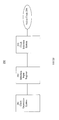
- FIG. 1 is a block diagram of exemplary clock signal selection system 100 in accordance with one embodiment of the present invention.
- Clock signal selection system 100 includes arbitration component 110 , control component 120 and selection component 130 .
- Arbitration component 110 is coupled to control component 120 which is coupled to selection component 130 .
- the components of clock signal selection system 100 cooperatively operate to select a clock signal as a active signal without reliance on an external master clock.
- Arbitration component 110 coordinates arbitration eligibility between a plurality of clock signals 171 , 172 and 173 .
- Control component 120 controls the coordination utilizing a clock signal from the plurality of clock signal 171 , 172 and 173 .
- a first one of the plurality of clock signals that is currently running is utilized for controlling the coordination and selection of a second one of the plurality of clock signals.
- Selection component 120 selects one of the plurality of signals and outputs as an active clock signal
- FIG. 2A is a block diagram of one exemplary clock signal selection system 200 in accordance with one embodiment of the present invention.
- Clock signal selection system 200 is similar to clock signal selection system 100 .
- Clock signal selection system 200 includes arbitration component 210 , control component 220 and selection component 230 .
- the components of clock signal selection system 200 cooperatively operate to select a clock signal utilizing a cross coupled feedback control and a one hot selection mechanism to select an active output clock signal.
- arbitration component 210 includes NOR gates 211 , 212 , and 213 , AND gates 214 , 215 , 2126 , and synchronizing components 217 , 218 , and 219 .
- the NOR gates 211 , 212 and 213 ensure the selection of one of the plurality of clock signals does not occur while another of the plurality of clock signals is selected.
- the AND gates 214 , 215 , and 216 coordinate the selection between the plurality of signals with selection of another of the plurality of signals.
- Synchronizing components 217 , 218 and 219 synchronizes a selected one of the plurality of clock signal, which helps avoid meta-stability in the selected output.
- cross coupling feedback is utilized to direct the arbitration by the arbitration component.
- control component 220 includes a flip flop for introducing a delay to mitigate runt pulse impact.
- the flip flop ensures a runt pulse does not pass the selection component OR gate between the time a first clock signal is gated off and the next active d or enabled clock being gated on.
- the control component also helps keep the high or low pulse of the resulting clock is no faster than either the clock that is being gated off nor the clock that is being gated on.
- the selection component is a multiplexer.
- the multiplexer includes a clock gate and an OR gate.
- the clock gate coordinates timing between a selection by the selection component and control component with a selected clock signal transition to avoid glitches.
- the clock gate includes a latch that opens for a portion of a clock cycle.
- the OR gate logically “ORs” clock signal output.
- FIG. 2B is a block diagram of exemplary clock system 290 in accordance with one embodiment of the present invention.
- Clock system 290 includes clock generation system 291 , selection input register 292 , and clock selection system 293 .
- Clock generation system 291 is coupled to selection input register 293 which in turn is coupled to clock selection system 293 .
- Clock generation system 291 generates a plurality of clock signals.
- clock generation system 291 includes a plurality of clock generation components.
- Clock selection system 293 selects between the plurality of clock signals, wherein the clock selection system utilizes cross coupling feedback of clock selection indications in controlling the selection between the plurality of clock signals The clock selection system performs the selecting while minimizing introduction of clock glitches and runt pluses.
- Selection input register 293 forwards the clock selection indications.
- selection input register 292 receives input in accordance with software controlled instructions.
- FIG. 3 is an exemplary timing diagram 300 in accordance with one embodiment of the present invention.
- Timing diagram 300 includes exemplary timing transitions for first clock signal 301 , enable signal 302 , first clock enable signal 303 , first clock gated signal 304 , first clock active signal 305 , second clock signal 311 , enable signal 312 , second clock enable signal 313 , second clock gated signal 314 , second clock active signal 315 , and active clock output 350 .
- an active output 350 signal corresponding to the frequency of first clock signal 301 is changed to a frequency corresponding to second clock signal 311 .
- active clock output 350 corresponds to first clock gated signal 304 up until time 321 and after the clock selection operations active clock output 350 corresponds to second clock gated signal 314 after time 331 .
- glitches on a decoded clock select line cause multiple clocks to be enabled when a non-active clock is currently selected. Registering the decoded “one-hot” selection signals before use avoids these glitches.
- the logic is skew tolerant and resulting skew does not affect the operation.
- the skew on the clock select decode signals is less than 1 cycle of the fastest clock period to avoid increase clock “hole' time.
- FIG. 4 is a flow chart of clock signal selection method 400 in accordance with one embodiment of the present invention.
- clock signal selection method 400 facilitates dynamic selection of different clock signals without an extra external dedicated clock signal for controlling the clocking of selection operations.
- clock signal method 400 utilizes incoming clock signals to control clocking of the clock signal selection operations.
- a plurality of clock signals and a plurality of corresponding clock selection indication signals are received.
- the plurality of clock signals can be received from a single source or a variety of sources.
- the clock signals operate at different frequencies and a different phase to one another.
- arbitration is performed on the plurality of selection indication signals to minimize conflict in selection of the active clock signal.
- the enabling and arbitrating utilizes feedback from a clock signal that is already running in selecting of another new clocksignal. The arbitrating ensures an enablement of one of the plurality of clock signals does not occur while another of the plurality of clock signals is enabled.
- an active clock signal from one of the plurality of clock signals to be output is enabled.
- the enabling is controlled by a clock included in the plurality of clock signals.
- timing between one of the plurality of clock signals being enabled and another of the plurality of clock signals being enabled prevents a runt pulse.
- the enabling and arbitrating includes changing from one of the plurality of clock signals to control the enabling and arbitrating to another of the plurality of clock signals to control the enabling and arbitrating.
- the enabling and arbitrating are tolerant of clock skew.
- FIG. 5A is a block diagram of exemplary computer system 500 in which clock selection can be performed in accordance with one embodiment of the present invention.
- Computer system 500 may provide the execution platform for implementing operations or certain software-based functionality of the present invention.
- the computer system 500 includes a CPU 501 coupled to a graphics processor 505 via a host interface 502 .
- the host interface 502 translates data and commands passing between the CPU 501 and the graphics processor 505 into their respective formats.
- Both the CPU 501 and the graphics processor 505 are coupled to a memory 521 via a memory controller 520 .
- the memory 521 is a shared memory, which refers to the property whereby the memory 521 stores instructions and data for both the CPU 501 and the graphics processor 505 . Access to the shared memory 521 is through the memory controller 520 .
- the shared memory 521 also stores data comprising a video frame buffer which drives a coupled display 525 .
- certain processes and steps of the present invention are realized, in one embodiment, as a series of instructions (e.g., software program) that reside within computer readable memory (e.g., memory 521 , CD, etc,) of a computer system (e.g., system 500 ) and are executed by the CPU 501 and graphics processor 505 of system 500 .
- system 500 shows the basic components of a computer system platform that may implement the functionality of the present invention. Accordingly, system 500 can be implemented as, for example, a number of different types of portable handheld electronic devices. Such devices can include, for example, portable phones, PDAs, handheld gaming devices, and the like. In such embodiments, components would be included that are designed to add peripheral buses, specialized communications components, support for specialized 10 devices, and the like.
- components 501 - 557 are depicted in FIGS. 5A and 5B as a discrete components, several of the components can be implemented as a single monolithic integrated circuit device (e.g., a single integrated circuit die) configured to take advantage of the high levels of integration provided by modern semiconductor fabrication processes.
- the CPU 501 , host interface 502 , graphics processor 505 , and memory controller 220 are fabricated as a single integrated circuit die.
- FIG. 5B shows a computer system 550 in which clock selection can be performed in accordance with one alternative embodiment of the present invention.
- Computer system 550 is substantially similar to computer system 500 of FIG. 5A .
- Computer system 550 utilizes the processor 551 having a dedicated system memory 552 , and the graphics processor 555 having a dedicated graphics memory 553 .
- Host interface 554 translates data and commands passing between the CPU 501 and the graphics processor 555 into their respective formats.
- the system memory 551 stores instructions and data for processes/threads executing on the CPU 551 and graphics memory 553 stores instructions and data for those processes/threads executing on the graphics processor 555 .
- the graphics memory 553 stores data for the video frame buffer which drives the display 557 .
- one or more of the components 551 - 553 of computer system 550 can be integrated onto a single integrated circuit die.
- present invention can be implemented in a variety of embodiments.
- Present clock selection systems and methods can be utilized in a number of different devices.
- the present invention can be utilized to select clocks in a game console, personal computer, personal digital assistant, cell phone, etc.
- the present invention can be utilized in systems that provide a variety of graphics applications (e.g., video games, movies, images, etc.) on any number of platforms. It is also appreciated that references to these applications or implementations are exemplary and the present invention is not limited to these examples.
- the present invention enables flexible selection of an active clock signals from a plurality of incoming clock signals utilizing.
- Utilization of a cross coupled feedback technique allows coordination of the selection of the active clock signal without a need for special sequencing of the interface signals controlled by a separate master clock signal.
- the selection of the active clock signal is performed efficiently while minimizing the clock glitch and runt pulse problems when changing clock sources.
Abstract
Description
Claims (20)
Priority Applications (1)
| Application Number | Priority Date | Filing Date | Title |
|---|---|---|---|
| US11/893,500 US9209792B1 (en) | 2007-08-15 | 2007-08-15 | Clock selection system and method |
Applications Claiming Priority (1)
| Application Number | Priority Date | Filing Date | Title |
|---|---|---|---|
| US11/893,500 US9209792B1 (en) | 2007-08-15 | 2007-08-15 | Clock selection system and method |
Publications (1)
| Publication Number | Publication Date |
|---|---|
| US9209792B1 true US9209792B1 (en) | 2015-12-08 |
Family
ID=54708415
Family Applications (1)
| Application Number | Title | Priority Date | Filing Date |
|---|---|---|---|
| US11/893,500 Active 2028-05-18 US9209792B1 (en) | 2007-08-15 | 2007-08-15 | Clock selection system and method |
Country Status (1)
| Country | Link |
|---|---|
| US (1) | US9209792B1 (en) |
Cited By (3)
| Publication number | Priority date | Publication date | Assignee | Title |
|---|---|---|---|---|
| US9773344B2 (en) | 2012-01-11 | 2017-09-26 | Nvidia Corporation | Graphics processor clock scaling based on idle time |
| US9811874B2 (en) | 2012-12-31 | 2017-11-07 | Nvidia Corporation | Frame times by dynamically adjusting frame buffer resolution |
| US20240094291A1 (en) * | 2022-09-16 | 2024-03-21 | Nvidia Corp. | Flexible one-hot decoding logic for clock controls |
Citations (70)
| Publication number | Priority date | Publication date | Assignee | Title |
|---|---|---|---|---|
| US4868832A (en) | 1986-04-30 | 1989-09-19 | Marrington S Paul | Computer power system |
| US5220660A (en) | 1990-06-28 | 1993-06-15 | Fujitsu Limited | Parallel data processing apparatus with signal skew compensation |
| US5331346A (en) | 1992-10-07 | 1994-07-19 | Panasonic Technologies, Inc. | Approximating sample rate conversion system |
| US5339445A (en) | 1992-11-16 | 1994-08-16 | Harris Corporation | Method of autonomously reducing power consumption in a computer sytem by compiling a history of power consumption |
| US5365468A (en) | 1992-02-17 | 1994-11-15 | Yamaha Corporation | Sampling frequency converter |
| US5510740A (en) | 1993-04-21 | 1996-04-23 | Intel Corporation | Method for synchronizing clocks upon reset |
| US5530845A (en) | 1992-05-13 | 1996-06-25 | Southwestern Bell Technology Resources, Inc. | Storage control subsystem implemented with an application program on a computer |
| US5586308A (en) | 1994-10-19 | 1996-12-17 | Advanced Micro Devices, Inc. | Clock control unit responsive to a power management state for clocking multiple clocked circuits connected thereto |
| US5652885A (en) | 1993-05-25 | 1997-07-29 | Storage Technology Corporation | Interprocess communications system and method utilizing shared memory for message transfer and datagram sockets for message control |
| US5737613A (en) | 1993-08-24 | 1998-04-07 | Mensch, Jr.; William D. | Method of operating microcomputer to minimize power dissipation while accessing slow memory |
| US5758133A (en) | 1995-12-28 | 1998-05-26 | Vlsi Technology, Inc. | System and method for altering bus speed based on bus utilization |
| US5811987A (en) * | 1995-06-02 | 1998-09-22 | Advanced Micro Devices, Inc. | Block clock and initialization circuit for a complex high density PLD |
| US5862368A (en) | 1996-12-11 | 1999-01-19 | Dell Usa, L.P. | Process to allow automatic microprocessor clock frequency detection and selection |
| US6057789A (en) | 1998-10-29 | 2000-05-02 | Neomagic Corp. | Re-synchronization of independently-clocked audio streams by dynamically switching among 3 ratios for sampling-rate-conversion |
| US6061410A (en) | 1997-02-27 | 2000-05-09 | Advanced Micro Devices | Frequency ratio estimation arrangement and method thereof |
| US6118462A (en) | 1997-07-01 | 2000-09-12 | Memtrax Llc | Computer system controller having internal memory and external memory control |
| US6134167A (en) | 1998-06-04 | 2000-10-17 | Compaq Computer Corporation | Reducing power consumption in computer memory |
| US6141737A (en) | 1995-10-11 | 2000-10-31 | Citrix Systems, Inc. | Method for dynamically and efficiently caching objects received from an application server by a client computer by subdividing cache memory blocks into equally-sized sub-blocks |
| US6163583A (en) | 1998-03-25 | 2000-12-19 | Sony Corporation Of Japan | Dynamic clocking apparatus and system for reducing power dissipation |
| US6216234B1 (en) | 1996-11-13 | 2001-04-10 | Intel Corporation | Processor having execution core sections operating at different clock rates |
| US6226661B1 (en) | 1998-11-13 | 2001-05-01 | Creative Technology Ltd. | Generation and application of sample rate conversion ratios using distributed jitter |
| US6252919B1 (en) | 1998-12-17 | 2001-06-26 | Neomagic Corp. | Re-synchronization of independently-clocked audio streams by fading-in with a fractional sample over multiple periods for sample-rate conversion |
| US6272649B1 (en) | 1998-09-28 | 2001-08-07 | Apple Computer, Inc. | Method and system for ensuring cache file integrity |
| US6275919B1 (en) | 1998-10-15 | 2001-08-14 | Creative Technology Ltd. | Memory storage and retrieval with multiple hashing functions |
| US20010044909A1 (en) | 2000-05-15 | 2001-11-22 | Lg Electronics Inc. | Method and apparatus for adjusting clock throttle rate based on usage of CPU |
| US20020013918A1 (en) | 1987-06-02 | 2002-01-31 | Swoboda Gary L. | Devices, systems and methods for mode driven stops |
| US6397340B2 (en) | 1989-10-30 | 2002-05-28 | Texas Instruments Incorporated | Real-time power conservation for electronic device having a processor |
| US20020145613A1 (en) | 1998-11-09 | 2002-10-10 | Broadcom Corporation | Graphics display system with color look-up table loading mechanism |
| US20030025689A1 (en) | 2001-05-02 | 2003-02-06 | Kim Jason Seung-Min | Power management system and method |
| US6539120B1 (en) | 1997-03-12 | 2003-03-25 | Matsushita Electric Industrial Co., Ltd. | MPEG decoder providing multiple standard output signals |
| US6549240B1 (en) | 1997-09-26 | 2003-04-15 | Sarnoff Corporation | Format and frame rate conversion for display of 24Hz source video |
| US6600345B1 (en) * | 2001-11-15 | 2003-07-29 | Analog Devices, Inc. | Glitch free clock select switch |
| US6600575B1 (en) | 1998-07-22 | 2003-07-29 | Oki Data Corporation | Clock supply circuit |
| US20030156639A1 (en) | 2002-02-19 | 2003-08-21 | Jui Liang | Frame rate control system and method |
| US6678831B1 (en) | 1997-12-11 | 2004-01-13 | Hewlett-Packard Development Company, L.P. | Managing power states in a computer system |
| US6690219B2 (en) * | 2001-09-06 | 2004-02-10 | Via Technologies, Inc. | Digital wave generating apparatus and the method thereof |
| US6690836B2 (en) | 1998-06-19 | 2004-02-10 | Equator Technologies, Inc. | Circuit and method for decoding an encoded version of an image having a first resolution directly into a decoded version of the image having a second resolution |
| US6728959B1 (en) | 1995-08-08 | 2004-04-27 | Novell, Inc. | Method and apparatus for strong affinity multiprocessor scheduling |
| US6748408B1 (en) * | 1999-10-21 | 2004-06-08 | International Buisness Machines Corporation | Programmable non-integer fractional divider |
| US6747581B2 (en) | 2002-02-01 | 2004-06-08 | Octiv, Inc. | Techniques for variable sample rate conversion |
| US6754837B1 (en) | 2000-07-17 | 2004-06-22 | Advanced Micro Devices, Inc. | Programmable stabilization interval for internal stop grant state during which core logic is supplied with clocks and power to minimize stabilization delay |
| US6775776B1 (en) | 2000-06-27 | 2004-08-10 | Intel Corporation | Biometric-based authentication in a nonvolatile memory device |
| US6804267B1 (en) | 1997-10-25 | 2004-10-12 | Centillium Communications, Inc. | Transceiver training for DSL modems under TCM-ISDN interference |
| US6816809B2 (en) | 2002-07-23 | 2004-11-09 | Hewlett-Packard Development Company, L.P. | Hardware based utilization metering |
| US6845456B1 (en) | 2001-05-01 | 2005-01-18 | Advanced Micro Devices, Inc. | CPU utilization measurement techniques for use in power management |
| US20050021656A1 (en) | 2003-07-21 | 2005-01-27 | Callegari Andres C. | System and method for network transmission of graphical data through a distributed application |
| US20050057551A1 (en) | 2003-09-01 | 2005-03-17 | Jin-Sheng Gong | Apparatus and method for image frame synchronization |
| US20050125705A1 (en) | 2003-12-04 | 2005-06-09 | Chih-Chuan Cheng | [method for dynamically adjusting cpu requency] |
| US20050216643A1 (en) | 2004-03-26 | 2005-09-29 | Munguia Peter R | Arbitration based power management |
| US6965974B1 (en) | 1997-11-14 | 2005-11-15 | Agere Systems Inc. | Dynamic partitioning of memory banks among multiple agents |
| US20050271361A1 (en) | 2004-05-19 | 2005-12-08 | Sachiyo Aoki | Image frame processing method and device for displaying moving images to a variety of displays |
| US7043649B2 (en) | 2002-11-20 | 2006-05-09 | Portalplayer, Inc. | System clock power management for chips with multiple processing modules |
| US7061409B1 (en) | 2005-02-07 | 2006-06-13 | Nokia Corporation | Techniques for sample rate conversion |
| US7100013B1 (en) | 2002-08-30 | 2006-08-29 | Nvidia Corporation | Method and apparatus for partial memory power shutoff |
| US7106224B2 (en) | 2002-08-14 | 2006-09-12 | Standard Microsystems Corporation | Communication system and method for sample rate converting data onto or from a network using a high speed frequency comparison technique |
| US7277101B2 (en) | 2003-09-29 | 2007-10-02 | Vixs Systems Inc | Method and system for scaling images |
| US20070240013A1 (en) | 2006-01-27 | 2007-10-11 | Sony Computer Entertainment Inc. | Methods And Apparatus For Managing Defective Processors Through Clock Programming |
| US20070257710A1 (en) * | 2005-05-06 | 2007-11-08 | Stmicroelectronics S.R.L. | Circuit to switch between clock signals and related method |
| US20080046774A1 (en) | 2006-08-15 | 2008-02-21 | Tyan Computer Corporation | Blade Clustering System with SMP Capability and Redundant Clock Distribution Architecture Thereof |
| US7414550B1 (en) | 2006-06-30 | 2008-08-19 | Nvidia Corporation | Methods and systems for sample rate conversion and sample clock synchronization |
| US7471120B2 (en) * | 2007-05-15 | 2008-12-30 | Broadcom Corporation | Clock switch for generation of multi-frequency clock signal |
| US20090204830A1 (en) | 2008-02-11 | 2009-08-13 | Nvidia Corporation | Power management with dynamic frequency dajustments |
| US7839410B1 (en) | 2006-07-28 | 2010-11-23 | Nvidia Corporation | Parameter buffer objects for shader parameters in a graphics library |
| US8013637B2 (en) * | 2007-03-20 | 2011-09-06 | Fujitsu Semiconductor Limited | Clock signal selection circuit |
| US20120188233A1 (en) | 2011-01-14 | 2012-07-26 | Brian Mark Shuster | Adaptable generation of virtual environment frames |
| US20120223940A1 (en) | 2011-03-01 | 2012-09-06 | Disney Enterprises, Inc. | Sprite strip renderer |
| US8327173B2 (en) | 2007-12-17 | 2012-12-04 | Nvidia Corporation | Integrated circuit device core power down independent of peripheral device operation |
| US20120306877A1 (en) | 2011-06-01 | 2012-12-06 | Apple Inc. | Run-Time Optimized Shader Program |
| US20130002838A1 (en) | 2010-04-20 | 2013-01-03 | Sony Computer Entertainment Inc. | Three-dimensional image playback method and three-dimensional image playback apparatus |
| US20130097443A1 (en) | 2011-10-12 | 2013-04-18 | Qualcomm Incorporated | Dynamic voltage and clock scaling control based on running average, variant and trend |
-
2007
- 2007-08-15 US US11/893,500 patent/US9209792B1/en active Active
Patent Citations (72)
| Publication number | Priority date | Publication date | Assignee | Title |
|---|---|---|---|---|
| US4868832A (en) | 1986-04-30 | 1989-09-19 | Marrington S Paul | Computer power system |
| US20020013918A1 (en) | 1987-06-02 | 2002-01-31 | Swoboda Gary L. | Devices, systems and methods for mode driven stops |
| US6397340B2 (en) | 1989-10-30 | 2002-05-28 | Texas Instruments Incorporated | Real-time power conservation for electronic device having a processor |
| US5220660A (en) | 1990-06-28 | 1993-06-15 | Fujitsu Limited | Parallel data processing apparatus with signal skew compensation |
| US5365468A (en) | 1992-02-17 | 1994-11-15 | Yamaha Corporation | Sampling frequency converter |
| US5530845A (en) | 1992-05-13 | 1996-06-25 | Southwestern Bell Technology Resources, Inc. | Storage control subsystem implemented with an application program on a computer |
| US5331346A (en) | 1992-10-07 | 1994-07-19 | Panasonic Technologies, Inc. | Approximating sample rate conversion system |
| US5339445A (en) | 1992-11-16 | 1994-08-16 | Harris Corporation | Method of autonomously reducing power consumption in a computer sytem by compiling a history of power consumption |
| US5510740A (en) | 1993-04-21 | 1996-04-23 | Intel Corporation | Method for synchronizing clocks upon reset |
| US5652885A (en) | 1993-05-25 | 1997-07-29 | Storage Technology Corporation | Interprocess communications system and method utilizing shared memory for message transfer and datagram sockets for message control |
| US5737613A (en) | 1993-08-24 | 1998-04-07 | Mensch, Jr.; William D. | Method of operating microcomputer to minimize power dissipation while accessing slow memory |
| US5586308A (en) | 1994-10-19 | 1996-12-17 | Advanced Micro Devices, Inc. | Clock control unit responsive to a power management state for clocking multiple clocked circuits connected thereto |
| US5811987A (en) * | 1995-06-02 | 1998-09-22 | Advanced Micro Devices, Inc. | Block clock and initialization circuit for a complex high density PLD |
| US6728959B1 (en) | 1995-08-08 | 2004-04-27 | Novell, Inc. | Method and apparatus for strong affinity multiprocessor scheduling |
| US6141737A (en) | 1995-10-11 | 2000-10-31 | Citrix Systems, Inc. | Method for dynamically and efficiently caching objects received from an application server by a client computer by subdividing cache memory blocks into equally-sized sub-blocks |
| US5758133A (en) | 1995-12-28 | 1998-05-26 | Vlsi Technology, Inc. | System and method for altering bus speed based on bus utilization |
| US6216234B1 (en) | 1996-11-13 | 2001-04-10 | Intel Corporation | Processor having execution core sections operating at different clock rates |
| US5862368A (en) | 1996-12-11 | 1999-01-19 | Dell Usa, L.P. | Process to allow automatic microprocessor clock frequency detection and selection |
| US6061410A (en) | 1997-02-27 | 2000-05-09 | Advanced Micro Devices | Frequency ratio estimation arrangement and method thereof |
| US6539120B1 (en) | 1997-03-12 | 2003-03-25 | Matsushita Electric Industrial Co., Ltd. | MPEG decoder providing multiple standard output signals |
| US6118462A (en) | 1997-07-01 | 2000-09-12 | Memtrax Llc | Computer system controller having internal memory and external memory control |
| US6549240B1 (en) | 1997-09-26 | 2003-04-15 | Sarnoff Corporation | Format and frame rate conversion for display of 24Hz source video |
| US6804267B1 (en) | 1997-10-25 | 2004-10-12 | Centillium Communications, Inc. | Transceiver training for DSL modems under TCM-ISDN interference |
| US6965974B1 (en) | 1997-11-14 | 2005-11-15 | Agere Systems Inc. | Dynamic partitioning of memory banks among multiple agents |
| US6678831B1 (en) | 1997-12-11 | 2004-01-13 | Hewlett-Packard Development Company, L.P. | Managing power states in a computer system |
| US6163583A (en) | 1998-03-25 | 2000-12-19 | Sony Corporation Of Japan | Dynamic clocking apparatus and system for reducing power dissipation |
| US6134167A (en) | 1998-06-04 | 2000-10-17 | Compaq Computer Corporation | Reducing power consumption in computer memory |
| US6690836B2 (en) | 1998-06-19 | 2004-02-10 | Equator Technologies, Inc. | Circuit and method for decoding an encoded version of an image having a first resolution directly into a decoded version of the image having a second resolution |
| US6600575B1 (en) | 1998-07-22 | 2003-07-29 | Oki Data Corporation | Clock supply circuit |
| US6272649B1 (en) | 1998-09-28 | 2001-08-07 | Apple Computer, Inc. | Method and system for ensuring cache file integrity |
| US6275919B1 (en) | 1998-10-15 | 2001-08-14 | Creative Technology Ltd. | Memory storage and retrieval with multiple hashing functions |
| US6057789A (en) | 1998-10-29 | 2000-05-02 | Neomagic Corp. | Re-synchronization of independently-clocked audio streams by dynamically switching among 3 ratios for sampling-rate-conversion |
| US20020145613A1 (en) | 1998-11-09 | 2002-10-10 | Broadcom Corporation | Graphics display system with color look-up table loading mechanism |
| US6226661B1 (en) | 1998-11-13 | 2001-05-01 | Creative Technology Ltd. | Generation and application of sample rate conversion ratios using distributed jitter |
| US6252919B1 (en) | 1998-12-17 | 2001-06-26 | Neomagic Corp. | Re-synchronization of independently-clocked audio streams by fading-in with a fractional sample over multiple periods for sample-rate conversion |
| US6748408B1 (en) * | 1999-10-21 | 2004-06-08 | International Buisness Machines Corporation | Programmable non-integer fractional divider |
| US20010044909A1 (en) | 2000-05-15 | 2001-11-22 | Lg Electronics Inc. | Method and apparatus for adjusting clock throttle rate based on usage of CPU |
| US6775776B1 (en) | 2000-06-27 | 2004-08-10 | Intel Corporation | Biometric-based authentication in a nonvolatile memory device |
| US6754837B1 (en) | 2000-07-17 | 2004-06-22 | Advanced Micro Devices, Inc. | Programmable stabilization interval for internal stop grant state during which core logic is supplied with clocks and power to minimize stabilization delay |
| US6845456B1 (en) | 2001-05-01 | 2005-01-18 | Advanced Micro Devices, Inc. | CPU utilization measurement techniques for use in power management |
| US20030025689A1 (en) | 2001-05-02 | 2003-02-06 | Kim Jason Seung-Min | Power management system and method |
| US6990594B2 (en) | 2001-05-02 | 2006-01-24 | Portalplayer, Inc. | Dynamic power management of devices in computer system by selecting clock generator output based on a current state and programmable policies |
| US6690219B2 (en) * | 2001-09-06 | 2004-02-10 | Via Technologies, Inc. | Digital wave generating apparatus and the method thereof |
| US6600345B1 (en) * | 2001-11-15 | 2003-07-29 | Analog Devices, Inc. | Glitch free clock select switch |
| US6747581B2 (en) | 2002-02-01 | 2004-06-08 | Octiv, Inc. | Techniques for variable sample rate conversion |
| US20030156639A1 (en) | 2002-02-19 | 2003-08-21 | Jui Liang | Frame rate control system and method |
| US6816809B2 (en) | 2002-07-23 | 2004-11-09 | Hewlett-Packard Development Company, L.P. | Hardware based utilization metering |
| US7106224B2 (en) | 2002-08-14 | 2006-09-12 | Standard Microsystems Corporation | Communication system and method for sample rate converting data onto or from a network using a high speed frequency comparison technique |
| US7100013B1 (en) | 2002-08-30 | 2006-08-29 | Nvidia Corporation | Method and apparatus for partial memory power shutoff |
| US7590815B1 (en) | 2002-08-30 | 2009-09-15 | Nvidia Corporation | Method and apparatus for partial memory power shutoff |
| US7043649B2 (en) | 2002-11-20 | 2006-05-09 | Portalplayer, Inc. | System clock power management for chips with multiple processing modules |
| US20050021656A1 (en) | 2003-07-21 | 2005-01-27 | Callegari Andres C. | System and method for network transmission of graphical data through a distributed application |
| US20050057551A1 (en) | 2003-09-01 | 2005-03-17 | Jin-Sheng Gong | Apparatus and method for image frame synchronization |
| US7277101B2 (en) | 2003-09-29 | 2007-10-02 | Vixs Systems Inc | Method and system for scaling images |
| US20050125705A1 (en) | 2003-12-04 | 2005-06-09 | Chih-Chuan Cheng | [method for dynamically adjusting cpu requency] |
| US20050216643A1 (en) | 2004-03-26 | 2005-09-29 | Munguia Peter R | Arbitration based power management |
| US20050271361A1 (en) | 2004-05-19 | 2005-12-08 | Sachiyo Aoki | Image frame processing method and device for displaying moving images to a variety of displays |
| US7061409B1 (en) | 2005-02-07 | 2006-06-13 | Nokia Corporation | Techniques for sample rate conversion |
| US20070257710A1 (en) * | 2005-05-06 | 2007-11-08 | Stmicroelectronics S.R.L. | Circuit to switch between clock signals and related method |
| US20070240013A1 (en) | 2006-01-27 | 2007-10-11 | Sony Computer Entertainment Inc. | Methods And Apparatus For Managing Defective Processors Through Clock Programming |
| US7414550B1 (en) | 2006-06-30 | 2008-08-19 | Nvidia Corporation | Methods and systems for sample rate conversion and sample clock synchronization |
| US7839410B1 (en) | 2006-07-28 | 2010-11-23 | Nvidia Corporation | Parameter buffer objects for shader parameters in a graphics library |
| US20080046774A1 (en) | 2006-08-15 | 2008-02-21 | Tyan Computer Corporation | Blade Clustering System with SMP Capability and Redundant Clock Distribution Architecture Thereof |
| US8013637B2 (en) * | 2007-03-20 | 2011-09-06 | Fujitsu Semiconductor Limited | Clock signal selection circuit |
| US7471120B2 (en) * | 2007-05-15 | 2008-12-30 | Broadcom Corporation | Clock switch for generation of multi-frequency clock signal |
| US8327173B2 (en) | 2007-12-17 | 2012-12-04 | Nvidia Corporation | Integrated circuit device core power down independent of peripheral device operation |
| US20090204830A1 (en) | 2008-02-11 | 2009-08-13 | Nvidia Corporation | Power management with dynamic frequency dajustments |
| US20130002838A1 (en) | 2010-04-20 | 2013-01-03 | Sony Computer Entertainment Inc. | Three-dimensional image playback method and three-dimensional image playback apparatus |
| US20120188233A1 (en) | 2011-01-14 | 2012-07-26 | Brian Mark Shuster | Adaptable generation of virtual environment frames |
| US20120223940A1 (en) | 2011-03-01 | 2012-09-06 | Disney Enterprises, Inc. | Sprite strip renderer |
| US20120306877A1 (en) | 2011-06-01 | 2012-12-06 | Apple Inc. | Run-Time Optimized Shader Program |
| US20130097443A1 (en) | 2011-10-12 | 2013-04-18 | Qualcomm Incorporated | Dynamic voltage and clock scaling control based on running average, variant and trend |
Non-Patent Citations (4)
| Title |
|---|
| Final Office Action Dated Feb. 17, 2011; U.S. Appl. No. 12/002,565. |
| Final Office Action; U.S. Appl. No. 12/002,565; Mail Date Mar. 16, 2012. |
| Non-Final Office Action; U.S. Appl. No. 12/002,565; Mail Date Oct. 20, 2011. |
| Office Action dated Sep. 17, 2010, U.S. Appl. No. 12/002,565. |
Cited By (4)
| Publication number | Priority date | Publication date | Assignee | Title |
|---|---|---|---|---|
| US9773344B2 (en) | 2012-01-11 | 2017-09-26 | Nvidia Corporation | Graphics processor clock scaling based on idle time |
| US9811874B2 (en) | 2012-12-31 | 2017-11-07 | Nvidia Corporation | Frame times by dynamically adjusting frame buffer resolution |
| US20240094291A1 (en) * | 2022-09-16 | 2024-03-21 | Nvidia Corp. | Flexible one-hot decoding logic for clock controls |
| US11940493B1 (en) * | 2022-09-16 | 2024-03-26 | Nvidia Corp. | Flexible one-hot decoding logic for clock controls |
Similar Documents
| Publication | Publication Date | Title |
|---|---|---|
| CA2658561C (en) | Low output skew double data rate serial encoder | |
| US7900078B1 (en) | Asynchronous conversion circuitry apparatus, systems, and methods | |
| KR101573850B1 (en) | Data processing system having a masking circuitry and method thereof | |
| US20080088492A1 (en) | Double data rate serial encoder | |
| JP2006268260A (en) | Data transfer controller and electronic equipment | |
| US9594700B2 (en) | Speculative memory controller | |
| US9672008B2 (en) | Pausible bisynchronous FIFO | |
| US20150089108A1 (en) | Clock signals for dynamic reconfiguration of communication link bundles | |
| US5537582A (en) | Bus interface circuitry for synchronizing central processors running at multiple clock frequencies to other computer system circuitry | |
| US20140281652A1 (en) | Data synchronization across asynchronous boundaries using selectable synchronizers to minimize latency | |
| US7526666B1 (en) | Derived clock synchronization for reduced skew and jitter | |
| US20160012802A1 (en) | Method of operating display driver integrated circuit and method of operating image processing system having the same | |
| JP2001332961A (en) | Clock-switching circuit | |
| US9209792B1 (en) | Clock selection system and method | |
| US20150102846A1 (en) | Distributing multiplexing logic to remove multiplexor latency on the output path for variable clock cycle, delayed signals | |
| US9164134B2 (en) | High-resolution phase detector | |
| US20060129720A1 (en) | Data buffer circuit, interface circuit and control method therefor | |
| JP2020513628A (en) | Clock gating enable generation | |
| JP2013127637A (en) | Method and apparatus for generating control signal for display panel driver | |
| US20130007314A1 (en) | First in first out device and method thereof | |
| US10564752B2 (en) | Gate driver and touch display apparatus thereof | |
| US10705558B2 (en) | Apparatuses and methods for avoiding glitches when switching clock sources | |
| US7589565B2 (en) | Low-power multi-output local clock buffer | |
| US7620798B1 (en) | Latency tolerant pipeline synchronization | |
| JP2006285724A (en) | Information processor and information processing method |
Legal Events
| Date | Code | Title | Description |
|---|---|---|---|
| AS | Assignment |
Owner name: NVIDIA CORPORATION, CALIFORNIA Free format text: ASSIGNMENT OF ASSIGNORS INTEREST;ASSIGNOR:BROWNING, GARY A.;REEL/FRAME:020029/0291 Effective date: 20071010 |
|
| STCF | Information on status: patent grant |
Free format text: PATENTED CASE |
|
| MAFP | Maintenance fee payment |
Free format text: PAYMENT OF MAINTENANCE FEE, 4TH YEAR, LARGE ENTITY (ORIGINAL EVENT CODE: M1551); ENTITY STATUS OF PATENT OWNER: LARGE ENTITY Year of fee payment: 4 |
|
| MAFP | Maintenance fee payment |
Free format text: PAYMENT OF MAINTENANCE FEE, 8TH YEAR, LARGE ENTITY (ORIGINAL EVENT CODE: M1552); ENTITY STATUS OF PATENT OWNER: LARGE ENTITY Year of fee payment: 8 |