US9121096B2 - Concentric showerhead for vapor deposition - Google Patents
Concentric showerhead for vapor deposition Download PDFInfo
- Publication number
- US9121096B2 US9121096B2 US12/576,797 US57679709A US9121096B2 US 9121096 B2 US9121096 B2 US 9121096B2 US 57679709 A US57679709 A US 57679709A US 9121096 B2 US9121096 B2 US 9121096B2
- Authority
- US
- United States
- Prior art keywords
- gas
- wafer
- reactor
- track
- channel
- Prior art date
- Legal status (The legal status is an assumption and is not a legal conclusion. Google has not performed a legal analysis and makes no representation as to the accuracy of the status listed.)
- Active, expires
Links
- 238000007740 vapor deposition Methods 0.000 title description 7
- 238000004891 communication Methods 0.000 claims abstract description 16
- 239000012530 fluid Substances 0.000 claims abstract description 16
- 238000005019 vapor deposition process Methods 0.000 claims abstract description 10
- ZOKXTWBITQBERF-UHFFFAOYSA-N Molybdenum Chemical compound [Mo] ZOKXTWBITQBERF-UHFFFAOYSA-N 0.000 claims description 14
- 239000000463 material Substances 0.000 claims description 14
- 229910052750 molybdenum Inorganic materials 0.000 claims description 14
- 239000011733 molybdenum Substances 0.000 claims description 14
- XEEYBQQBJWHFJM-UHFFFAOYSA-N Iron Chemical compound [Fe] XEEYBQQBJWHFJM-UHFFFAOYSA-N 0.000 claims description 12
- PXHVJJICTQNCMI-UHFFFAOYSA-N Nickel Chemical compound [Ni] PXHVJJICTQNCMI-UHFFFAOYSA-N 0.000 claims description 12
- 239000010935 stainless steel Substances 0.000 claims description 10
- 229910001220 stainless steel Inorganic materials 0.000 claims description 10
- 229910001182 Mo alloy Inorganic materials 0.000 claims description 7
- VYZAMTAEIAYCRO-UHFFFAOYSA-N Chromium Chemical compound [Cr] VYZAMTAEIAYCRO-UHFFFAOYSA-N 0.000 claims description 6
- 229910000831 Steel Inorganic materials 0.000 claims description 6
- 229910045601 alloy Inorganic materials 0.000 claims description 6
- 239000000956 alloy Substances 0.000 claims description 6
- 229910052804 chromium Inorganic materials 0.000 claims description 6
- 239000011651 chromium Substances 0.000 claims description 6
- 229910052742 iron Inorganic materials 0.000 claims description 6
- 229910052759 nickel Inorganic materials 0.000 claims description 6
- 239000010959 steel Substances 0.000 claims description 6
- 230000008021 deposition Effects 0.000 abstract description 119
- 235000012431 wafers Nutrition 0.000 description 297
- 239000007789 gas Substances 0.000 description 252
- 238000005229 chemical vapour deposition Methods 0.000 description 126
- 238000000151 deposition Methods 0.000 description 125
- 239000000758 substrate Substances 0.000 description 123
- 238000000034 method Methods 0.000 description 63
- 238000007373 indentation Methods 0.000 description 56
- 238000010438 heat treatment Methods 0.000 description 49
- IJGRMHOSHXDMSA-UHFFFAOYSA-N Atomic nitrogen Chemical compound N#N IJGRMHOSHXDMSA-UHFFFAOYSA-N 0.000 description 46
- 238000002955 isolation Methods 0.000 description 44
- JBRZTFJDHDCESZ-UHFFFAOYSA-N AsGa Chemical compound [As]#[Ga] JBRZTFJDHDCESZ-UHFFFAOYSA-N 0.000 description 34
- 229910001218 Gallium arsenide Inorganic materials 0.000 description 34
- 238000000429 assembly Methods 0.000 description 25
- 230000000712 assembly Effects 0.000 description 25
- 229910052757 nitrogen Inorganic materials 0.000 description 23
- VYPSYNLAJGMNEJ-UHFFFAOYSA-N silicon dioxide Inorganic materials O=[Si]=O VYPSYNLAJGMNEJ-UHFFFAOYSA-N 0.000 description 20
- 238000002347 injection Methods 0.000 description 18
- 239000007924 injection Substances 0.000 description 18
- FTWRSWRBSVXQPI-UHFFFAOYSA-N alumanylidynearsane;gallanylidynearsane Chemical compound [As]#[Al].[As]#[Ga] FTWRSWRBSVXQPI-UHFFFAOYSA-N 0.000 description 17
- 239000000356 contaminant Substances 0.000 description 16
- 238000005137 deposition process Methods 0.000 description 15
- 238000009792 diffusion process Methods 0.000 description 15
- 239000000203 mixture Substances 0.000 description 15
- UFHFLCQGNIYNRP-UHFFFAOYSA-N Hydrogen Chemical compound [H][H] UFHFLCQGNIYNRP-UHFFFAOYSA-N 0.000 description 14
- 239000001257 hydrogen Substances 0.000 description 14
- 229910052739 hydrogen Inorganic materials 0.000 description 14
- 239000010453 quartz Substances 0.000 description 12
- 238000012545 processing Methods 0.000 description 11
- BHEPBYXIRTUNPN-UHFFFAOYSA-N hydridophosphorus(.) (triplet) Chemical compound [PH] BHEPBYXIRTUNPN-UHFFFAOYSA-N 0.000 description 10
- 238000002156 mixing Methods 0.000 description 9
- MDPILPRLPQYEEN-UHFFFAOYSA-N aluminium arsenide Chemical compound [As]#[Al] MDPILPRLPQYEEN-UHFFFAOYSA-N 0.000 description 8
- 239000002243 precursor Substances 0.000 description 8
- 230000008646 thermal stress Effects 0.000 description 7
- GYHNNYVSQQEPJS-UHFFFAOYSA-N Gallium Chemical compound [Ga] GYHNNYVSQQEPJS-UHFFFAOYSA-N 0.000 description 6
- GPXJNWSHGFTCBW-UHFFFAOYSA-N Indium phosphide Chemical compound [In]#P GPXJNWSHGFTCBW-UHFFFAOYSA-N 0.000 description 6
- 230000003247 decreasing effect Effects 0.000 description 6
- 230000000694 effects Effects 0.000 description 6
- 229910052733 gallium Inorganic materials 0.000 description 6
- 230000001965 increasing effect Effects 0.000 description 6
- 238000001505 atmospheric-pressure chemical vapour deposition Methods 0.000 description 5
- 230000009977 dual effect Effects 0.000 description 5
- 238000002161 passivation Methods 0.000 description 5
- XKRFYHLGVUSROY-UHFFFAOYSA-N Argon Chemical compound [Ar] XKRFYHLGVUSROY-UHFFFAOYSA-N 0.000 description 4
- OKTJSMMVPCPJKN-UHFFFAOYSA-N Carbon Chemical compound [C] OKTJSMMVPCPJKN-UHFFFAOYSA-N 0.000 description 4
- RBFQJDQYXXHULB-UHFFFAOYSA-N arsane Chemical compound [AsH3] RBFQJDQYXXHULB-UHFFFAOYSA-N 0.000 description 4
- 229910002804 graphite Inorganic materials 0.000 description 4
- 239000010439 graphite Substances 0.000 description 4
- 238000013459 approach Methods 0.000 description 3
- 238000006243 chemical reaction Methods 0.000 description 3
- 238000011109 contamination Methods 0.000 description 3
- 230000004907 flux Effects 0.000 description 3
- 230000001939 inductive effect Effects 0.000 description 3
- 239000000377 silicon dioxide Substances 0.000 description 3
- 208000012868 Overgrowth Diseases 0.000 description 2
- PNEYBMLMFCGWSK-UHFFFAOYSA-N aluminium oxide Inorganic materials [O-2].[O-2].[O-2].[Al+3].[Al+3] PNEYBMLMFCGWSK-UHFFFAOYSA-N 0.000 description 2
- 229910052786 argon Inorganic materials 0.000 description 2
- 239000000919 ceramic Substances 0.000 description 2
- 238000005530 etching Methods 0.000 description 2
- 239000005350 fused silica glass Substances 0.000 description 2
- 238000005424 photoluminescence Methods 0.000 description 2
- 239000007787 solid Substances 0.000 description 2
- 230000035882 stress Effects 0.000 description 2
- 239000010409 thin film Substances 0.000 description 2
- QVGXLLKOCUKJST-UHFFFAOYSA-N atomic oxygen Chemical compound [O] QVGXLLKOCUKJST-UHFFFAOYSA-N 0.000 description 1
- 239000000969 carrier Substances 0.000 description 1
- 229910010293 ceramic material Inorganic materials 0.000 description 1
- 239000004020 conductor Substances 0.000 description 1
- 238000001816 cooling Methods 0.000 description 1
- 239000010408 film Substances 0.000 description 1
- 230000005484 gravity Effects 0.000 description 1
- 239000011261 inert gas Substances 0.000 description 1
- 238000005339 levitation Methods 0.000 description 1
- 238000012423 maintenance Methods 0.000 description 1
- 229910052751 metal Inorganic materials 0.000 description 1
- 239000002184 metal Substances 0.000 description 1
- 239000001301 oxygen Substances 0.000 description 1
- 229910052760 oxygen Inorganic materials 0.000 description 1
- 238000010926 purge Methods 0.000 description 1
- 239000000376 reactant Substances 0.000 description 1
- 239000004065 semiconductor Substances 0.000 description 1
- 239000000243 solution Substances 0.000 description 1
- 239000000126 substance Substances 0.000 description 1
- 238000002230 thermal chemical vapour deposition Methods 0.000 description 1
- 238000011144 upstream manufacturing Methods 0.000 description 1
- 239000012808 vapor phase Substances 0.000 description 1
Images


Classifications
-
- C—CHEMISTRY; METALLURGY
- C23—COATING METALLIC MATERIAL; COATING MATERIAL WITH METALLIC MATERIAL; CHEMICAL SURFACE TREATMENT; DIFFUSION TREATMENT OF METALLIC MATERIAL; COATING BY VACUUM EVAPORATION, BY SPUTTERING, BY ION IMPLANTATION OR BY CHEMICAL VAPOUR DEPOSITION, IN GENERAL; INHIBITING CORROSION OF METALLIC MATERIAL OR INCRUSTATION IN GENERAL
- C23C—COATING METALLIC MATERIAL; COATING MATERIAL WITH METALLIC MATERIAL; SURFACE TREATMENT OF METALLIC MATERIAL BY DIFFUSION INTO THE SURFACE, BY CHEMICAL CONVERSION OR SUBSTITUTION; COATING BY VACUUM EVAPORATION, BY SPUTTERING, BY ION IMPLANTATION OR BY CHEMICAL VAPOUR DEPOSITION, IN GENERAL
- C23C16/00—Chemical coating by decomposition of gaseous compounds, without leaving reaction products of surface material in the coating, i.e. chemical vapour deposition [CVD] processes
- C23C16/22—Chemical coating by decomposition of gaseous compounds, without leaving reaction products of surface material in the coating, i.e. chemical vapour deposition [CVD] processes characterised by the deposition of inorganic material, other than metallic material
- C23C16/30—Deposition of compounds, mixtures or solid solutions, e.g. borides, carbides, nitrides
- C23C16/301—AIII BV compounds, where A is Al, Ga, In or Tl and B is N, P, As, Sb or Bi
-
- C—CHEMISTRY; METALLURGY
- C23—COATING METALLIC MATERIAL; COATING MATERIAL WITH METALLIC MATERIAL; CHEMICAL SURFACE TREATMENT; DIFFUSION TREATMENT OF METALLIC MATERIAL; COATING BY VACUUM EVAPORATION, BY SPUTTERING, BY ION IMPLANTATION OR BY CHEMICAL VAPOUR DEPOSITION, IN GENERAL; INHIBITING CORROSION OF METALLIC MATERIAL OR INCRUSTATION IN GENERAL
- C23C—COATING METALLIC MATERIAL; COATING MATERIAL WITH METALLIC MATERIAL; SURFACE TREATMENT OF METALLIC MATERIAL BY DIFFUSION INTO THE SURFACE, BY CHEMICAL CONVERSION OR SUBSTITUTION; COATING BY VACUUM EVAPORATION, BY SPUTTERING, BY ION IMPLANTATION OR BY CHEMICAL VAPOUR DEPOSITION, IN GENERAL
- C23C16/00—Chemical coating by decomposition of gaseous compounds, without leaving reaction products of surface material in the coating, i.e. chemical vapour deposition [CVD] processes
- C23C16/44—Chemical coating by decomposition of gaseous compounds, without leaving reaction products of surface material in the coating, i.e. chemical vapour deposition [CVD] processes characterised by the method of coating
- C23C16/455—Chemical coating by decomposition of gaseous compounds, without leaving reaction products of surface material in the coating, i.e. chemical vapour deposition [CVD] processes characterised by the method of coating characterised by the method used for introducing gases into reaction chamber or for modifying gas flows in reaction chamber
- C23C16/45519—Inert gas curtains
-
- C—CHEMISTRY; METALLURGY
- C23—COATING METALLIC MATERIAL; COATING MATERIAL WITH METALLIC MATERIAL; CHEMICAL SURFACE TREATMENT; DIFFUSION TREATMENT OF METALLIC MATERIAL; COATING BY VACUUM EVAPORATION, BY SPUTTERING, BY ION IMPLANTATION OR BY CHEMICAL VAPOUR DEPOSITION, IN GENERAL; INHIBITING CORROSION OF METALLIC MATERIAL OR INCRUSTATION IN GENERAL
- C23C—COATING METALLIC MATERIAL; COATING MATERIAL WITH METALLIC MATERIAL; SURFACE TREATMENT OF METALLIC MATERIAL BY DIFFUSION INTO THE SURFACE, BY CHEMICAL CONVERSION OR SUBSTITUTION; COATING BY VACUUM EVAPORATION, BY SPUTTERING, BY ION IMPLANTATION OR BY CHEMICAL VAPOUR DEPOSITION, IN GENERAL
- C23C16/00—Chemical coating by decomposition of gaseous compounds, without leaving reaction products of surface material in the coating, i.e. chemical vapour deposition [CVD] processes
- C23C16/44—Chemical coating by decomposition of gaseous compounds, without leaving reaction products of surface material in the coating, i.e. chemical vapour deposition [CVD] processes characterised by the method of coating
- C23C16/455—Chemical coating by decomposition of gaseous compounds, without leaving reaction products of surface material in the coating, i.e. chemical vapour deposition [CVD] processes characterised by the method of coating characterised by the method used for introducing gases into reaction chamber or for modifying gas flows in reaction chamber
- C23C16/45563—Gas nozzles
- C23C16/45565—Shower nozzles
-
- C—CHEMISTRY; METALLURGY
- C23—COATING METALLIC MATERIAL; COATING MATERIAL WITH METALLIC MATERIAL; CHEMICAL SURFACE TREATMENT; DIFFUSION TREATMENT OF METALLIC MATERIAL; COATING BY VACUUM EVAPORATION, BY SPUTTERING, BY ION IMPLANTATION OR BY CHEMICAL VAPOUR DEPOSITION, IN GENERAL; INHIBITING CORROSION OF METALLIC MATERIAL OR INCRUSTATION IN GENERAL
- C23C—COATING METALLIC MATERIAL; COATING MATERIAL WITH METALLIC MATERIAL; SURFACE TREATMENT OF METALLIC MATERIAL BY DIFFUSION INTO THE SURFACE, BY CHEMICAL CONVERSION OR SUBSTITUTION; COATING BY VACUUM EVAPORATION, BY SPUTTERING, BY ION IMPLANTATION OR BY CHEMICAL VAPOUR DEPOSITION, IN GENERAL
- C23C16/00—Chemical coating by decomposition of gaseous compounds, without leaving reaction products of surface material in the coating, i.e. chemical vapour deposition [CVD] processes
- C23C16/44—Chemical coating by decomposition of gaseous compounds, without leaving reaction products of surface material in the coating, i.e. chemical vapour deposition [CVD] processes characterised by the method of coating
- C23C16/455—Chemical coating by decomposition of gaseous compounds, without leaving reaction products of surface material in the coating, i.e. chemical vapour deposition [CVD] processes characterised by the method of coating characterised by the method used for introducing gases into reaction chamber or for modifying gas flows in reaction chamber
- C23C16/45563—Gas nozzles
- C23C16/45576—Coaxial inlets for each gas
-
- C—CHEMISTRY; METALLURGY
- C23—COATING METALLIC MATERIAL; COATING MATERIAL WITH METALLIC MATERIAL; CHEMICAL SURFACE TREATMENT; DIFFUSION TREATMENT OF METALLIC MATERIAL; COATING BY VACUUM EVAPORATION, BY SPUTTERING, BY ION IMPLANTATION OR BY CHEMICAL VAPOUR DEPOSITION, IN GENERAL; INHIBITING CORROSION OF METALLIC MATERIAL OR INCRUSTATION IN GENERAL
- C23C—COATING METALLIC MATERIAL; COATING MATERIAL WITH METALLIC MATERIAL; SURFACE TREATMENT OF METALLIC MATERIAL BY DIFFUSION INTO THE SURFACE, BY CHEMICAL CONVERSION OR SUBSTITUTION; COATING BY VACUUM EVAPORATION, BY SPUTTERING, BY ION IMPLANTATION OR BY CHEMICAL VAPOUR DEPOSITION, IN GENERAL
- C23C16/00—Chemical coating by decomposition of gaseous compounds, without leaving reaction products of surface material in the coating, i.e. chemical vapour deposition [CVD] processes
- C23C16/44—Chemical coating by decomposition of gaseous compounds, without leaving reaction products of surface material in the coating, i.e. chemical vapour deposition [CVD] processes characterised by the method of coating
- C23C16/458—Chemical coating by decomposition of gaseous compounds, without leaving reaction products of surface material in the coating, i.e. chemical vapour deposition [CVD] processes characterised by the method of coating characterised by the method used for supporting substrates in the reaction chamber
- C23C16/4582—Rigid and flat substrates, e.g. plates or discs
- C23C16/4583—Rigid and flat substrates, e.g. plates or discs the substrate being supported substantially horizontally
-
- C—CHEMISTRY; METALLURGY
- C23—COATING METALLIC MATERIAL; COATING MATERIAL WITH METALLIC MATERIAL; CHEMICAL SURFACE TREATMENT; DIFFUSION TREATMENT OF METALLIC MATERIAL; COATING BY VACUUM EVAPORATION, BY SPUTTERING, BY ION IMPLANTATION OR BY CHEMICAL VAPOUR DEPOSITION, IN GENERAL; INHIBITING CORROSION OF METALLIC MATERIAL OR INCRUSTATION IN GENERAL
- C23C—COATING METALLIC MATERIAL; COATING MATERIAL WITH METALLIC MATERIAL; SURFACE TREATMENT OF METALLIC MATERIAL BY DIFFUSION INTO THE SURFACE, BY CHEMICAL CONVERSION OR SUBSTITUTION; COATING BY VACUUM EVAPORATION, BY SPUTTERING, BY ION IMPLANTATION OR BY CHEMICAL VAPOUR DEPOSITION, IN GENERAL
- C23C16/00—Chemical coating by decomposition of gaseous compounds, without leaving reaction products of surface material in the coating, i.e. chemical vapour deposition [CVD] processes
- C23C16/44—Chemical coating by decomposition of gaseous compounds, without leaving reaction products of surface material in the coating, i.e. chemical vapour deposition [CVD] processes characterised by the method of coating
- C23C16/48—Chemical coating by decomposition of gaseous compounds, without leaving reaction products of surface material in the coating, i.e. chemical vapour deposition [CVD] processes characterised by the method of coating by irradiation, e.g. photolysis, radiolysis, particle radiation
- C23C16/481—Chemical coating by decomposition of gaseous compounds, without leaving reaction products of surface material in the coating, i.e. chemical vapour deposition [CVD] processes characterised by the method of coating by irradiation, e.g. photolysis, radiolysis, particle radiation by radiant heating of the substrate
-
- C—CHEMISTRY; METALLURGY
- C23—COATING METALLIC MATERIAL; COATING MATERIAL WITH METALLIC MATERIAL; CHEMICAL SURFACE TREATMENT; DIFFUSION TREATMENT OF METALLIC MATERIAL; COATING BY VACUUM EVAPORATION, BY SPUTTERING, BY ION IMPLANTATION OR BY CHEMICAL VAPOUR DEPOSITION, IN GENERAL; INHIBITING CORROSION OF METALLIC MATERIAL OR INCRUSTATION IN GENERAL
- C23C—COATING METALLIC MATERIAL; COATING MATERIAL WITH METALLIC MATERIAL; SURFACE TREATMENT OF METALLIC MATERIAL BY DIFFUSION INTO THE SURFACE, BY CHEMICAL CONVERSION OR SUBSTITUTION; COATING BY VACUUM EVAPORATION, BY SPUTTERING, BY ION IMPLANTATION OR BY CHEMICAL VAPOUR DEPOSITION, IN GENERAL
- C23C16/00—Chemical coating by decomposition of gaseous compounds, without leaving reaction products of surface material in the coating, i.e. chemical vapour deposition [CVD] processes
- C23C16/44—Chemical coating by decomposition of gaseous compounds, without leaving reaction products of surface material in the coating, i.e. chemical vapour deposition [CVD] processes characterised by the method of coating
- C23C16/54—Apparatus specially adapted for continuous coating
-
- Y—GENERAL TAGGING OF NEW TECHNOLOGICAL DEVELOPMENTS; GENERAL TAGGING OF CROSS-SECTIONAL TECHNOLOGIES SPANNING OVER SEVERAL SECTIONS OF THE IPC; TECHNICAL SUBJECTS COVERED BY FORMER USPC CROSS-REFERENCE ART COLLECTIONS [XRACs] AND DIGESTS
- Y10—TECHNICAL SUBJECTS COVERED BY FORMER USPC
- Y10T—TECHNICAL SUBJECTS COVERED BY FORMER US CLASSIFICATION
- Y10T137/00—Fluid handling
- Y10T137/8593—Systems
- Y10T137/87571—Multiple inlet with single outlet
Definitions
- Embodiments of the invention generally relate to methods and apparatuses for vapor deposition, and more particularly, to chemical vapor deposition processes and chambers.
- Chemical vapor deposition is the deposition of a thin film on a substrate by the reaction of vapor phase chemicals. Chemical vapor deposition reactors are used to deposit thin films of various compositions on the substrate. CVD is highly utilized in many activities, such as the semiconductor industry.
- CVD reactors There are numerous types of CVD reactors for very different applications. For example, one type of reactor includes atmospheric pressure reactors and another type of reactor includes low-pressure reactors. These distinct designs address a variety of challenges that are encountered during a CVD process, such as depletion effects, contamination issues, and reactor maintenance.
- Embodiments of the invention generally relate to a concentric gas manifold assembly used in a vapor deposition reactor or system.
- the concentric gas manifold assembly may be used in a reactor or system for growing epitaxial films in a continuous manner.
- the concentric gas manifold assembly for vapor deposition processes is provided which includes lower, middle, and upper sections.
- the upper section is coupled to the middle section and the middle section is coupled to the lower section.
- the middle section contains a first gas inlet, a first gas manifold extending from the first gas inlet to a first passageway, and a tube extending along a central axis and containing a first channel along the central axis.
- the first passageway may be in fluid communication with the first channel.
- the lower section contains a second gas inlet, a second gas manifold extending from the second gas inlet to a second passageway, and an opening concentric with the central axis.
- the tube extends to the opening to form a second channel between the tube and an edge of the opening.
- the second channel may be concentric with the central axis, and the second passageway may be in fluid communication with the second channel.
- the tube has a cylindrical geometry and the opening has a circular geometry. In other examples, the tube extends through the opening and past a lower surface of the lower section.
- the second channel usually extends parallel to the first channel and the central axis.
- Each of the upper section, the middle section, and the lower section may independently contain or be made from molybdenum, molybdenum alloys, steel, stainless steel, nickel, chromium, iron, or alloys thereof.
- the tube may contain or be made from molybdenum, molybdenum alloys, steel, stainless steel, nickel, chromium, iron, or alloys thereof.
- a method for forming a material on a substrate surface contains positioning a substrate below a gas manifold assembly during a vapor deposition process and flowing a first process gas along a first gas flow path of a middle section of the gas manifold assembly.
- the middle section may contain a first gas inlet, a first gas manifold extending from the first gas inlet to a first passageway, and a tube extending along a central axis and containing a first channel along the central axis, wherein the first passageway is in fluid communication with the first channel.
- the method further includes flowing a second process gas along a second gas flow path of a lower section of the gas manifold assembly, the lower section comprises and exposing the substrate to the first process gas and the second process gas while depositing a material thereon.
- the lower section may contain a second gas inlet, a second gas manifold extending from the second gas inlet to a second passageway, and an opening concentric with the central axis, wherein the tube extends to the opening to form a second channel between the tube and an edge of the opening, the second channel is concentric with the central axis, and the second passageway is in fluid communication with the second channel.
- the method further provides that the second process gas encompasses the first process gas while flowing between the gas manifold assembly and the substrate.
- the gas manifold assembly may further contain an upper section coupled to the middle section and the middle section is coupled to the lower section.
- the vapor deposition process may be a thermal CVD process.
- the vapor deposition reactor or system containing a concentric gas manifold assembly which includes an entrance isolator operable to prevent contaminants from entering the system at an entrance of the system, an exit isolator operable to prevent contaminants from entering the system at an exit of the system, a intermediate isolator disposed between the entrance and exit isolators, a first deposition zone disposed adjacent the entrance isolator, a second deposition zone disposed adjacent the exit isolator, and the concentric gas manifold assembly coupled with and in fluid communication with the first deposition zone.
- an entrance isolator operable to prevent contaminants from entering the system at an entrance of the system
- an exit isolator operable to prevent contaminants from entering the system at an exit of the system
- a intermediate isolator disposed between the entrance and exit isolators
- a first deposition zone disposed adjacent the entrance isolator
- a second deposition zone disposed adjacent the exit isolator
- the concentric gas manifold assembly coupled with and in fluid communication
- the concentric gas manifold assembly coupled with the vapor deposition reactor or system further has a middle section containing a first gas inlet, a first gas manifold extending from the first gas inlet to a first passageway, and a tube extending along a central axis and containing a first channel along the central axis.
- the first passageway may be in fluid communication with the first channel.
- the concentric gas manifold assembly may have a lower section containing a second gas inlet, a second gas manifold extending from the second gas inlet to a second passageway, and an opening concentric with the central axis.
- the tube may extend to the opening to form a second channel between the tube and an edge of the opening, the second channel is concentric with the central axis, and the second passageway is in fluid communication with the second channel.
- the concentric gas manifold assembly may further have an upper section coupled to the middle section and the middle section may be coupled to the lower section.
- the tube may have a cylindrical geometry and the opening has a circular geometry.
- the tube extends through the opening and past a lower surface of the lower section.
- the second channel extends parallel to the first channel and the central axis.
- the intermediate isolator is disposed between the deposition zones and is operable to prevent mixing of gases between the first deposition zone and the second deposition zone.
- the vapor deposition reactor or system containing the concentric gas manifold assembly may have a gas injected into the entrance isolator at a first flow rate to prevent back diffusion of gases from the first deposition zone.
- the gas may be injected into the intermediate isolator at a first flow rate to prevent back mixing of gases between the first deposition zone and the second deposition zone.
- Another gas may be injected into the exit isolator at a first flow rate to prevent contaminants from entering the system at the exit of the system.
- the vapor deposition reactor or system may further have an exhaust disposed adjacent each isolator and operable to exhaust gases injected by the isolators.
- the exhaust may be disposed adjacent each deposition zone and operable to exhaust gases injected into the deposition zones.
- FIG. 1A depicts a chemical vapor deposition reactor according to one embodiment of the invention
- FIG. 1B depicts a perspective view of a reactor lid assembly according to one embodiment of the invention
- FIG. 2 depicts a side perspective view of the chemical vapor deposition (CVD) reactor according to one embodiment described herein;
- FIG. 3 depicts a reactor lid assembly of the CVD reactor according to one embodiment described herein;
- FIG. 4A depicts a top view of a top plate of the CVD reactor according to another embodiment described herein;
- FIGS. 4B-4E depict a gas manifold assembly according to another embodiment described herein;
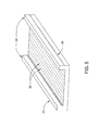
- FIG. 5 depicts a wafer carrier track of the CVD reactor according to one embodiment described herein;
- FIG. 6 depicts a front view of the wafer carrier track of the CVD reactor according to one embodiment described herein;
- FIG. 7 depicts a side view of the wafer carrier track of the CVD reactor according to one embodiment described herein;
- FIG. 8 depicts a perspective view of the wafer carrier track of the CVD reactor according to one embodiment described herein;
- FIG. 9 depicts the reactor lid assembly and the wafer carrier track of the CVD reactor according to one embodiment described herein;
- FIG. 10A depicts a CVD reactor according to one embodiment described herein;
- FIGS. 10B-10C depict a levitating wafer carrier according to another embodiment described herein;
- FIGS. 10D-10F depict other levitating wafer carriers according to another embodiment described herein;
- FIG. 11 depicts a first layout of the CVD reactor according to one embodiment described herein;
- FIG. 12 depicts a second layout of the CVD reactor according to one embodiment described herein;
- FIG. 13 depicts a third layout of the CVD reactor according to one embodiment described herein;
- FIG. 14 depicts a fourth layout of the CVD reactor according to one embodiment described herein;
- FIG. 15 depicts a fifth layout of the CVD reactor according to one embodiment described herein;
- FIG. 16 depicts a sixth layout of the CVD reactor according to one embodiment described herein;
- FIG. 17 depicts a seventh layout of the CVD reactor according to one embodiment described herein.
- FIG. 18 depicts flow path configurations of the CVD reactor according to one embodiment described herein.
- Embodiments of the invention generally relate to an apparatus and a method of chemical vapor deposition (“CVD”). As set forth herein, embodiments of the invention is described as they relate to an atmospheric pressure CVD reactor and metal-organic precursor gases. It is to be noted, however, that aspects of the invention are not limited to use with an atmospheric pressure CVD reactor or metal-organic precursor gases, but are applicable to other types of reactor systems and precursor gases. To better understand the novelty of the apparatus of the invention and the methods of use thereof, reference is hereafter made to the accompanying drawings.
- an atmospheric pressure CVD reactor may be used to provide multiple epitaxial layers on a substrate, such as a wafer, such as a gallium arsenide wafer. These epitaxial layers may include aluminum gallium arsenide, gallium arsenide, and phosphorous gallium arsenide. These epitaxial layers may be grown on the gallium arsenide wafer for later removal so that the wafer may be reused to generate additional materials.
- the CVD reactor may be used to provide solar cells. These solar cells may further include single junction, heterojunction, or other configurations.
- the CVD reactor may be configured to develop a wafer which produces about 2.5 watts and has the dimension of about 10 cm by about 10 cm. In one embodiment, the CVD reactor may provide a throughput range of about 1 wafer per minute to about 10 wafers per minute.
- FIG. 1A shows a CVD reactor 10 , according to one embodiment of the invention.
- the reactor 10 includes a reactor lid assembly 20 , a wafer carrier track 30 , a wafer carrier track support 40 , and a heating lamp assembly 50 .
- the reactor lid assembly 20 may be formed from molybdenum, molybdenum alloys, stainless steel, and quartz.
- the reactor lid assembly 20 is disposed on the wafer carrier track 30 .
- the wafer carrier track 30 may be formed from quartz, molybdenum, silica (such as fused silica), alumina, or other ceramic materials.
- the wafer carrier track 30 may be seated in a wafer carrier track support 40 .
- the wafer carrier track support 40 may be formed from quartz or a metal, such as molybdenum, molybdenum alloys, steel, stainless steel, nickel, chromium, iron, or alloys thereof.
- a heating lamp assembly 50 (further discussed below with respect to FIG. 10 ) is disposed below the wafer carrier track support 40 .
- the overall CVD reactor length may be in a range of about 18 feet to about 25 feet, but may extend beyond this range for different applications.
- FIGS. 2 , 3 , and 4 A provide various views of embodiments of the reactor lid assembly 20 .
- the reactor lid assembly 20 forms a rectangular body having sidewalls 25 extending from the bottom surface of the reactor lid assembly 20 , and having a plurality of raised portions 26 centrally located between the sidewalls 25 .
- the raised portions 26 may extend from the bottom surface of the top plate at different lengths along the reactor lid assembly 20 .
- the raised portions 26 are disposed between the sidewalls 25 so that clearances are formed between the raised portions 26 and each sidewall 25 . These clearances may be used to help couple the reactor lid assembly 20 to the track 30 (further described below). Both the sidewalls 25 and the raised portions 26 may extend substantially the longitudinal length of the reactor lid assembly 20 .
- the reactor lid assembly 20 may be formed as a single solid structural component, or it may be constructed from several segments coupled together.
- the raised portions 26 may vary in length and number, thereby forming “zones” which may be utilized for different applications in a CVD process.
- the reactor lid assembly 20 may also include multiple patterns of raised portions 26 along its length, such as to develop numerous layouts or stages in a CVD process.
- FIG. 3 also shows the reactor lid assembly 20 .
- the reactor lid assembly 20 as shown in FIG. 3 may represent an entire top plate structure or a single segment of a larger constructed top plate structure.
- a plurality of ports 21 disposed through the top surface of the reactor lid assembly 20 and centrally located along the longitudinal axis of the reactor lid assembly 20 .
- the ports 21 may vary in size, shape, number, and location along the top surface of the reactor lid assembly 20 .
- the ports 21 may be used as injection, deposition, and/or exhaust ports for communicating a gas, into the CVD reactor.
- each port 21 is disposed between two adjacent raised portions 26 (as show in FIG.
- a gas may be injected into a port 21 so that the gas first travels along the sides of the adjacent raised portions 26 and then travels along the bottom surfaces of the raised portions 26 and into the flow path of a substrate.
- the sidewalls 25 are enclosed at the ends of the reactor lid assembly 20 to encapsulate any fluids that are communicated to the “zones” and “paths” created by the ports 21 and the raised portions 26 of the reactor lid assembly 20 .
- FIG. 4A shows a top view of the reactor lid assembly 20 having deposition ports 23 , injection ports 22 , and exhaust ports 24 .
- the deposition ports 23 may be fitted with removable showerheads or gas manifold assemblies to facilitate distribution of a gas, into the CVD reactor, and specifically to uniformly apply the gas to a substrate passing beneath the showerhead.
- the showerheads may include injection hole diameters in the range of about 0.1 millimeters to about 5 millimeters, and may include injection hole spacing in the range of about 1 millimeter to about 30 millimeters. These dimensions may extend beyond these ranges for different applications.
- the showerheads and the reactor lid assembly 20 may be configured to provide a high reactant utilization, meaning that the gases utilized in the reactor are consumed by the reactions during the CVD process.
- FIGS. 4B-4E depict the gas manifold assembly 11 which may be fitted to a deposition port 23 in other embodiments herein.
- the gas manifold assembly 11 may be fitted to injection ports 22 for flowing various gases (e.g., Ar or N 2 ) into a chamber, reactor, or system while forming isolation curtains.
- the gas manifold assembly 11 may be fitted to exhaust ports 24 for flowing gases from the chamber, reactor, or system by a vacuum system or pump.
- the injection ports 22 and the exhaust ports 24 may be used to develop “isolation curtains” to help prevent contamination and to help prevent back diffusion of the gases introduced into the CVD reactor 10 between the various zones created in the reactor. These “isolation curtains” may be introduced at the front end (entrance) and the back end (exit) of the CVD reactor 10 , as well as between the various zones created within the CVD reactor 10 .
- nitrogen or argon may be injected into an injection port 22 to purge contaminants, such as oxygen, out of a particular zone, which are then exhausted out of an adjacent exhaust port 24 .
- the CVD reactor 10 limits the gas isolation to a two dimension configuration that protects between zones and isolates the reactor from outside contaminants, such as air.
- FIGS. 4B-4E depict a gas manifold assembly 11 which may be used in the CVD reactor 10 according other embodiments described herein.
- the gas manifold assembly 11 contains an upper section 27 , a middle section 28 , and a lower section 29 .
- the middle section 28 is coupled between the upper section 27 and the lower section 29 .
- the middle section 28 contains a gas inlet 28 A in fluid communication and coupled with gas manifold 13 .
- the lower section 29 contains a gas inlet 29 A in fluid communication and coupled with gas manifold 14 .
- the middle section 28 contains a tube 19 , which extends from the middle section 28 to the opening 29 C of the lower section 29 . Opening 29 C extends completely through the lower section 29 .
- the channel 18 extends between the outer surface of the tube 19 and the inner surface of the opening 29 C.
- the tube 19 contains a channel 17 extending therethrough.
- channels 17 and 18 and tube 19 are concentric with each other and positioned along a common axis, such as the central axis 12 .
- the middle section 28 and the tube 19 are separate pieces which are coupled together.
- the middle section 28 and the tube 19 are a single piece formed together.
- Each of the upper section 27 , the middle section 28 , the lower section 29 , and the tube 19 may independently contain a material or is formed from the same material or different materials, such as molybdenum, molybdenum alloys, steel, stainless steel, nickel, chromium, iron, alloys thereof, or combinations thereof.
- the gas manifold assembly 11 contains at least two independent and exclusive gas flow paths, as illustrated in FIG. 4E .
- a first gas flow path extends from the gas inlet 28 A, through the gas manifold 13 of the middle section 28 , through passageways 15 , and into the channel 17 of the tube 19 .
- a second gas flow path extends from the gas inlet 29 A, through the gas manifold 14 of the lower section 29 , through passageways 16 , and into the channel 18 formed between the opening 29 C and the tube 19 .
- the first and second gas flow paths are concentric and flow parallel to the central axis 12 , as described in one embodiment herein.
- the first and second gas flow paths remain independent with the second gas flow path encompassing the first gas flow path. Therefore, two process gases, which are chemically reactive towards each other, may be simultaneously delivered to a substrate by flowing one of the process gases along the first gas flow path and flowing the other process gas along the second gas flow path. The two process gases do not mix or do not substantially combine while exiting the gas manifold assembly 11 .
- an inert gas may be flowed along the second gas flow path and be used as an isolation curtain to a process gas flowing along the first gas flow path.
- the lower surface 28 B of the tube 19 is flush with the lower surface 29 B of lower section 29 , as depicted in FIGS. 4B-4E .
- the tube 19 has a longer length such that the lower surface 28 B protrudes from opening 29 C and past the horizontal plane of the lower surface 29 B of lower section 29 .
- the tube 19 has a shorter length such that the lower surface 28 B does not protrude from the opening 29 C or past the horizontal plane of the lower surface 29 B of lower section 29 .
- FIGS. 4B-4E depict the tube 19 as having a cylindrical shape and the opening 29 C as being round, in other examples, the tube 19 and/or the opening 29 C may have alternative shapes or geometries.
- the tube 19 and the opening 29 C may be rectangular or square.
- the gas manifold assembly 11 may have additional sections, such as a second middle section or a third middle section. Each additional middle section may be similar to the middle section 28 , but have a tube having a larger or smaller diameter than the tube 19 .
- Each additional middle section may be positioned above or below the middle section 28 , such as between the middle section 28 and the upper section 27 or between the middle section 28 and the lower section 29 .
- Each additional tube containing a channel may be positioned along the central axis 12 and be concentric with the channel 18 and the tube 19 . Therefore, each additional middle section has a gas flow path independent and separate form the first and second gas flow paths. Each additional gas flow path extends from a gas inlet, through a gas manifold of the additional middle section, a passageway, and into the channel within the additional tube.
- FIGS. 2 , 5 , 6 , 7 , and 8 provide various views of embodiments of the wafer carrier track 30 .
- the wafer carrier track 30 may provide a levitation-type system so that a wafer may float across a cushion of a gas, such as nitrogen or argon, supplied from the gas holes 33 of the wafer carrier track 30 .
- the wafer carrier track 30 generally may be a rectangular body having an upper portion 31 and a lower portion 32 .
- the upper portion 31 includes side surfaces 35 extending from the top surface of the wafer carrier track 30 and disposed along the longitudinal length of the wafer carrier track 30 , thereby forming a “guide path” along which a wafer travels through the CVD reactor.
- the width of the guide path (e.g. the distance between the inner sides of the side surfaces 35 ) may be in a range of about 110 millimeters to about 130 millimeters, the height of the guide path may be in a range of about 30 millimeters to about 50 millimeters, and the length of the guide path may be in a range of about 970 millimeters to about 1030 millimeters, however, these dimensions may extend beyond these ranges for different applications.
- the upper portion 31 may include a recessed bottom surface, and the bottom section may include a recessed top surface, such that when joined together, a gas cavity 36 is formed therebetween.
- the gas cavity 36 may be used to circulate and distribute gas that is injected into the gas cavity 36 to the guide path of the wafer carrier track 30 to generate the cushion of gas.
- the number, size, shape, and location of the gas cavity 36 along the wafer carrier track 30 may vary. Both the side surfaces 35 and the gas cavity 36 may extent substantially the longitudinal length of the wafer carrier track 30 .
- the wafer carrier track 30 may be formed as a single solid structural component, or it may be constructed from several segments coupled together. In one embodiment, the wafer carrier track 30 may be tilted at an angle, such that the entrance is elevated above the exit, so that the wafers may float down the track with the aid of gravity.
- the side surfaces 35 of the wafer carrier track 30 may be received into the gaps formed between the raised portions 26 and the flange members 25 of the reactor lid assembly 20 to enclose the “guide path” along the wafer carrier track 30 and to further compassing the “zones” formed with the raised portions 26 along the wafer carrier track 30 .
- FIG. 5 shows an embodiment of the wafer carrier track 30 .
- wafer carrier track 30 includes a plurality of gas holes 33 along the guide path of the wafer carrier track 30 and between the side surfaces 35 .
- the gas holes 33 may be uniformly disposed along the guide path of the wafer carrier track 30 in multiple rows.
- the diameter of the gas holes 33 may include a range of about 0.2 millimeters to about 0.10 millimeters and the pitch of the gas holes 33 may include a range of about 10 millimeters to about 30 millimeters, but these dimensions may extend beyond these ranges for different applications.
- the number, size, shape, and location of the gas holes 33 along the wafer carrier track 30 may vary.
- the gas holes 33 may include rows of rectangular slits or slots disposed along the guide path of the wafer carrier track 30 .
- Gas holes 33 are in communication with the gas cavity 36 disposed beneath the guide path of the wafer carrier track 30 . Gas that is supplied to the gas cavity 36 is uniformly released through the gas holes 33 to develop a cushion of gas along the wafer carrier track 30 .
- a wafer positioned on the guide path of the wafer carrier track 30 may be levitated by the gas supplied from underneath and easily transported along the guide path of the wafer carrier track 30 .
- the gap between a levitated wafer and the guide path of the wafer carrier track 30 may be greater than about 0.05 millimeters, but may vary depending on different applications. This levitation-type system reduces any drag effects produced by continuous direct contact with the guide path of the wafer carrier track 30 .
- gas ports 34 may be provided along the sides of the side surfaces 35 adjacent the guide path of the wafer carrier track 30 . These gas ports 34 may be used as an exhaust for the gas that is supplied through the gas holes 33 . Alternatively, these gas ports 34 may be used to inject gas laterally into the center of the wafer carrier track 30 to help stabilize and center a wafer that is floating along the guide path of the wafer carrier track 30 . In an alternative embodiment, the guide path of the wafer carrier track 30 may include a tapered profile to help stabilize and center a wafer that is floating along the guide path of the wafer carrier track 30 .
- FIG. 6 shows a front view embodiment of the wafer carrier track 30 .
- the wafer carrier track 30 includes the upper portion 31 and the lower portion 32 .
- the upper portion 31 includes side surfaces 35 that form the “guide path” along the length of the wafer carrier track 30 .
- the upper portion 31 may further include side surfaces 35 that form recessed portions 39 between the sides of the side surfaces 35 . These recessed portions 39 may be adapted to receive the flange members 25 of the reactor lid assembly 20 (shown in FIG. 2 ) to couple the reactor lid assembly 20 and the wafer carrier track 30 together and enclose the guide path along the wafer carrier track 30 .
- Also show in FIG. 5 are gas holes 33 extending from the guide path of the wafer carrier track 30 to the gas cavity 36 .
- the lower portion 32 may act as a support for the upper portion 31 and may include a recessed bottom surface.
- An injection line 38 may be connected to the lower portion 32 so that gas may be injected through the line 38 and into the gas cavity 36 .
- FIG. 7 shows a side view of the wafer carrier track 30 having a single injection line 38 into a gas cavity 36 along the entire wafer carrier track 30 length.
- the wafer carrier track 30 may include multiple gas cavities 36 and multiple injection lines 38 along its length.
- the wafer carrier track 30 may include multiple segments, each segment having a single gas cavity and a single injection line 38 .
- the wafer carrier track 30 may include combinations of the above described gas cavity 36 and injection line 38 configurations.
- FIG. 8 shows a cross sectional perspective view embodiment of the wafer carrier track 30 having the upper portion 31 and the lower portion 32 .
- the upper portion 31 having side surfaces 35 , gas holes 33 , and the gas cavity 36 disposed on the lower portion 32 .
- the side surfaces 35 and the lower portion 32 are hollow, which may substantially reduce the weight of the wafer carrier track 30 and may enhance the thermal control of the wafer carrier track 30 relative to the wafers traveling along the wafer carrier track 30 .
- FIG. 9 shows the reactor lid assembly 20 coupled to or with the wafer carrier track 30 .
- O-rings may be used to seal the reactor lid assembly 20 and wafer carrier track 30 interfaces.
- the entrance into the CVD reactor 10 may be sized to receive varying sizes of wafers.
- a gap 60 formed between the raised portions 26 of the reactor lid assembly 20 and the guide path of the wafer carrier track 30 , in which the wafer is received, is dimensioned to help prevent contaminants from entering the CVD reactor 10 at either end, dimensioned to help prevent back diffusion of gases between zones, and dimensioned to help ensure that the gases supplied to the wafer during the CVD process are uniformly distributed across the thickness of the gap and across the wafer.
- the gap 60 may be formed between the lower surface of the reactor lid assembly 20 and the guide path of the wafer carrier track 30 , In one embodiment, the gap 60 may be formed between the lower surface of the gas manifold assemblies and the guide path of the wafer carrier track 30 , In one embodiment, the gap 60 may be in the range of about 0.5 millimeters to about 5 millimeters in thickness and may vary along the length of the reactor lid assembly 20 and wafer carrier track 30 . In one embodiment, the wafer may have a length in the range of about 50 millimeters to about 150 millimeters, a width in the range of about 50 millimeters to about 150 millimeters, and a thickness in the range of about 0.5 millimeters to about 5 millimeters.
- the wafer may include a base layer having individual strips of layers disposed on the base layer.
- the individual strips are treated in the CVD process. These individual strips may have a length of about 10 cm and a width of about 1 cm (although other sizes may be utilized as well), and may be formed in this manner to facilitate removal of the treated strips from the wafer and to reduce the stresses induced upon the treated strips during the CVD process.
- the CVD reactor 10 may be adapted to receive wafers having dimensions that extend beyond the above recited ranges for different applications.
- the CVD reactor 10 may be adapted to provide an automatic and continuous feed and exit of wafers into and out of the reactor, such as with a conveyor-type system.
- a wafer may be fed into the CVD reactor 10 at one end of the reactor, by a conveyor for example, communicated through a CVD process, and removed at the opposite end of the reactor, by a retriever for example, using a manual and/or automated system.
- the CVD reactor 10 may be adapted to produce wafers in the range of one wafer about every 10 minutes to one wafer about every 10 seconds, and may extend beyond this range for different applications. In one embodiment, the CVD reactor 10 may be adapted to produce 6-10 treated wafers per minute.
- FIG. 10A shows an alternative embodiment of a CVD reactor 100 .
- the CVD reactor 100 includes a reactor body 120 , a wafer carrier track 130 , a wafer carrier 140 , and a heating lamp assembly 150 .
- the reactor body 120 may form a rectangular body and may be contain molybdenum, quartz, stainless steel, or other similar material.
- the reactor body 120 may enclose the wafer carrier track 130 and extend substantially the length of the wafer carrier track 130 .
- the wafer carrier track 130 may also form a rectangular body and may contain quartz or other low thermal conductive material to assist with temperature distribution during the CVD process.
- the wafer carrier track 130 may be configured to provide a levitation-type system that supplies a cushion of gas to communicate a wafer along the wafer carrier track 130 .
- a conduit such as a gas cavity 137 having a v-shaped roof 135 is centrally located along the longitudinal axis of the guide path of the wafer carrier track 130 .
- Gas is supplied through gas cavity 137 and is injected through gas holes in the roof 135 to supply the cushion of gas that floats a wafer having a corresponding v-shaped notch (not shown) on its bottom surface along the wafer carrier track 130 .
- the reactor body 120 and the wafer carrier track 130 each are a single structural component.
- the reactor body 120 includes multiple segments coupled together to form a complete structural component.
- the wafer carrier track 130 includes multiple segments coupled together to form a complete structural component.
- a wafer carrier 140 adapted to carry a single wafer (not shown) or strips 160 of a wafer along the wafer carrier track 130 .
- the wafer carrier 140 may be formed from graphite or other similar material.
- the wafer carrier 140 may have a v-shaped notch 136 along its bottom surface to correspond with the v-shaped roof 135 of the wafer carrier track 130 .
- the v-shaped notch 136 disposed over the v-shaped roof 135 helps guide the wafer carrier 140 along the wafer carrier track 130 .
- the wafer carrier 140 may be used to carry the wafer strips 160 through the CVD process to help reduce the thermal stresses imparted on the wafer during the process.
- Gas holes in the roof 135 of the gas cavity 137 may direct a cushion of gas along the bottom of the wafer carrier 140 , which utilizes the corresponding v-shaped feature to help stabilize and center the wafer carrier 140 , and thus the strips 160 of wafer, during the CVD process.
- a wafer may be provided in strips 160 to facilitate removal of the treated strips from the wafer carrier 140 and to reduce the stresses induced upon the strips during the CVD process.
- FIGS. 10B-10F depict a wafer carrier 70 which may be used to carry a wafer through a variety of processing chambers including the CVD reactors as described herein, as well as other processing chambers used for deposition or etching.
- the wafer carrier 70 has short sides 71 , long sides 73 , an upper surface 72 , and a lower surface 74 .
- the wafer carrier 70 is illustrated with a rectangular geometry, but may also have a square geometry, a circular geometry, or other geometries.
- the wafer carrier 70 may contain or be formed from graphite or other materials.
- the wafer carrier 70 usually travels through the CVD reactor with the short sides 71 facing forward while the long sides 73 face towards the sides of the CVD reactor.
- FIG. 10B illustrates a top view of the wafer carrier 70 containing 3 indentations 75 on the upper surface 72 .
- Wafers may be positioned within the indentations 75 while being transferred through the CVD reactor during a process.
- the upper surface 72 may have more or less indentations, including no indentations.
- the upper surface 72 of the wafer carrier 70 may contain 0, 1, 2, 3, 4, 5, 6, 7, 8, 9, 10, 12, or more indentations for containing wafers.
- one or multiple wafers may be disposed directly on the upper surface 72 which does not have an indentation.
- FIG. 10C illustrates a bottom view of the wafer carrier 70 containing the indentation 78 on the lower surface 74 , as described in one embodiment herein.
- the indentation 78 may be used to help levitate the wafer carrier 70 upon the introduction of a gas cushion under the wafer carrier 70 .
- a gas flow may be directed at the indentation 78 , which accumulates gas to form the gas cushion.
- the lower surface 74 of the wafer carrier 70 may have no indentations, or may have one indentation 78 ( FIG. 10C ), two indentations 78 ( FIGS. 10D-10F ), three indentations 78 (not shown) or more.
- the indentation 78 may have straight or tapered sides.
- the indentation 78 has tapered sides such that the sides 76 are steeper or more abrupt than the sides 77 which have more of a gradual change of angle.
- the sides 77 within the indentation 78 may be tapered to compensate for a thermal gradient across the wafer carrier 70 .
- the indentation 78 has straight sides and tapered sides such that the sides 76 are straight and the sides 77 have a taper or the sides 77 are straight and the sides 76 have a taper.
- the indentation 78 may have all straight sides such that the sides 76 and 77 are straight.
- FIGS. 10D-10F illustrate bottom views of the wafer carrier 70 containing two indentations 78 on the lower surface 74 .
- the two indentations 78 help levitate the wafer carrier 70 upon the introduction of a gas cushion under the wafer carrier 70 .
- a gas flow may be directed at the indentations 78 , which accumulates gas to form the gas cushion.
- the indentations 78 may have straight or tapered sides.
- the indentations 78 have all straight sides such that the sides 76 and 77 are straight, e.g., perpendicular to the plane of the lower surface 74 .
- FIG. 10E the indentations 78 have all straight sides such that the sides 76 and 77 are straight, e.g., perpendicular to the plane of the lower surface 74 .
- the indentations 78 have all tapered sides such that the sides 76 are steeper or more abrupt than the sides 77 which have more of a gradual change of angle.
- the sides 77 within the indentations 78 may be tapered to compensate for a thermal gradient across the wafer carrier 70 .
- the indentations 78 may have a combination of straight sides and tapered sides such that the sides 76 are straight and the sides 77 have a taper or the sides 77 are straight and the sides 76 have a taper.
- the wafer carrier 70 contains a heat flux which extends from the lower surface 74 to the upper surface 72 and to any wafers disposed thereon.
- the heat flux may be controlled by both the internal pressure and length of the processing system.
- the profile of wafer carrier 70 may be tapered to compensate the heat loses from other sources. During a process, heat is lost through the edges of the wafer carrier 70 , such as the short sides 71 and the long sides 73 . However, the heat lost may be compensated by allowing more heat flux into the edges of the wafer carrier 70 by reducing the gap of the guide path in the levitation.
- FIG. 10A also depicts the reactor body 120 disposed on the heating lamp assembly 150 .
- the heating lamp assembly 150 may be configured to control the temperature profile within the CVD reactor by increasing and decreasing the temperature of the reactor body 120 , the wafer carrier track 130 , and specifically the wafer, along the length of the CVD reactor.
- the heating lamp assembly 150 may include a plurality of heating lamps disposed along the longitudinal length of the wafer carrier track 130 .
- the heating lamp assembly 150 includes individually controlled heating lamps disposed along the length of the wafer carrier track 130 .
- the heating lamp assembly 150 includes a bank of heating lamps that are movable and follow a wafer as it travels along the wafer carrier track 130 .
- the embodiments of the heating lamp assembly 150 may also be used as the heating lamp assembly 50 , described above with respect to FIG. 1 .
- a heating assembly may include resistive heating elements, such as resistive heaters, which may be individually controlled along the length of the wafer carrier track 130 .
- a resistive heating element may be bonded to or painted onto the reactor body 120 , the wafer carrier track 130 , or the wafer carrier 140 .
- another type of heating assembly that may be utilized to heat the reactor body 120 is an inductive heating element, such as with a radio frequency power source (not shown). The inductive heating element may be coupled to or with the reactor body 120 , the wafer carrier track 130 , and/or the wafer carrier 140 .
- Embodiments of the various types of heating assemblies (including heating lamp assemblies 50 and 150 ) described herein may be utilized independently or in combination with the CVD reactor.
- the heating lamp assembly 150 may be configured to heat a wafer in the CVD reactor to a temperature within a range from about 300° C. to about 800° C. In one embodiment, the heating lamp assembly 150 may be configured to raise the temperature of the wafer to an appropriate process temperature prior to introduction into a deposition zone of the CVD reactor. In one embodiment, the heating lamp assembly 150 may be configured with the CVD reactor to bring the wafer to a temperature within a range from about 300° C. to about 800° C. prior to introduction into a deposition zone of the CVD reactor.
- the wafer may be heated to within a process temperature range prior to entering one or more deposition zones of the CVD reactor to facilitate the deposition processes, and the temperature of the wafer may be maintained within the process temperature range as the wafer passes through the one or more deposition zones.
- the wafer may be heated to and maintained within the process temperature range as it moves along the wafer carrier track.
- a center temperature to an edge temperature of the wafer may be within 10° C. of each other.
- FIGS. 11-17 illustrate various configurations of CVD processes that can be utilized with the CVD reactor as described herein.
- FIG. 11 illustrates a first configuration 200 , having an entrance isolator assembly 220 , a first isolator assembly 230 , a second isolator assembly 240 , a third isolator assembly 250 , and an exit isolator assembly 260 .
- a plurality of deposition zones 290 may be located along the wafer carrier track of the CVD reactor and may be surrounded by the isolator assemblies. Between each of these isolator assemblies, one or more exhausts 225 may be provided to remove any gases that are supplied to the wafer at each isolator assembly or deposition zone.
- a precursor gas may be injected at the entrance isolator assembly 220 , which follows a two dimensional flow path, e.g. down to the wafer and then along the length of the wafer carrier track, indicated by flow path 210 for example.
- the gas is then exhausted up through exhaust 225 , which may be provided on each side of the isolator assembly 220 .
- the gas may be directed at the entrance isolator assembly 220 and then along the length of the wafer carrier track, indicated by flow path 215 for example, to prevent contaminants from entering the entrance of the CVD reactor.
- Gas injected at the intermediate isolator assemblies may travel upstream from the flow of the wafer, indicated by flow path 219 for example. This back diffusion of gas may be received through the adjacent exhaust to prevent contaminants or mixing of gases between zones along the wafer carrier track of the CVD reactor.
- the flow rate of the gases injected through the isolator assemblies, e.g. along flow path 210 , in the direction of the wafer flow may also be adapted to further prevent back diffusion from entering the isolation zone.
- the laminar flow along flow path 210 may be flowed at different flow rates to meet any back diffusion of gas, for example at junction 217 below exhaust 225 , to prevent the back diffusion of gas from isolator assembly 230 from entering the isolation zone developed by isolator assembly 220 .
- the wafer may be heated to within a process temperature range as it travels along the wafer carrier track prior to entering the deposition zones 290 .
- the temperature of the wafer may be maintained within the process temperature range as it travels along the wafer carrier track through the deposition zones 290 .
- the wafer may be cooled to within a specific temperature range upon exiting the deposition zones 290 as it travels along the remainder of the wafer carrier track.
- the lengths of the isolation zones and the deposition zones may be varied to reduce the effects of back diffusion of gases.
- the lengths of the isolation zones created may range from about 1 meter to about 2 meters in length but may extend beyond this range for different applications.
- the flow rates of the gases injected from the isolator assemblies may also be varied to reduce the effects of back diffusion of gases.
- the entrance isolator assembly 220 and the exit isolator assembly 260 may supply a precursor gas at about 30 liters per minute, while the first 230 , second 240 , and third 250 isolator assemblies may supply a precursor gas at about 3 liters per minute.
- the precursor gas supplied at the entrance isolator assembly 220 and the exit isolator assembly 260 may include nitrogen.
- the precursor gas supplied at the first 230 , second 240 , and third 250 isolator assemblies may include arsine.
- two isolator assemblies may supply a total of about 6 liters per minute of nitrogen.
- three isolator assemblies may supply a total of about 9 liters per minute of arsine.
- the gap e.g. the thickness between the guide path of the wafer carrier track and the raised portion of the reactor lid assembly, alternatively, the thickness of the space through which wafer travels into and out of the CVD reactor, of the isolation zones may also be varied to reduce the effects of back diffusion of gases.
- the isolator gap may be in a range of about 0.1 millimeters to about 5 millimeters.
- FIG. 18 illustrates several flow path configurations 900 which may be provided by the CVD reactor.
- the flow path configurations 900 may be used for injecting a gas through one or more isolator assemblies, injecting a gas into a deposition zone, and/or exhausting a gas from isolation and/or deposition zones.
- Dual flow path configuration 910 shows a gas directed in the same direction as the flow path of the wafer, as well as in the opposite direction of the flow path of the wafer.
- a larger volume of flow may be directed through the dual flow path configuration 910 due to the wider flow area 911 .
- This wider flow area 911 may be adapted for use with the other embodiments described herein.
- Single flow path configuration 920 shows a gas directed in a single direction, which may be in the same or opposite direction of the flow path of the wafer.
- a low volume of flow may be directed through the single flow path configuration 920 due to the narrow flow area 921 .
- This narrower flow area 921 may be adapted for use with the other embodiments described herein.
- Exhaust flow path configuration 930 shows that gas may be exhausted from adjacent zones through a wider flow area 931 , such as adjacent isolation zones, adjacent deposition zones, or an isolation zone adjacent to a deposition zone.
- first exhaust/injector flow path configuration 940 shows a dual flow path configuration 941 having a narrow flow area 943 disposed between an exhaust flow path 944 and a single injection flow path 945 . Also shown is a narrower gap 942 portion along which the wafer may travel through the CVD reactor. As described above, the gap 942 may vary along the wafer carrier track of the CVD reactor, thereby allowing a gas to be directly and uniformly injected onto the surface of the wafer. This narrower gap 942 portion may be used to provide full consumption or near full consumption of the gas injected onto the wafer during a reaction in a deposition zone. In addition, the gap 942 may be used to facilitate thermal control during the isolation and/or deposition process. A gas injected in the narrower gap 942 portion may maintain a higher temperature as it is injected onto the wafer.
- a second exhaust/injector flow path configuration 950 provides a first exhaust flow path 954 having a wide flow area, a first dual flow path configuration 951 having a narrow gap portion 952 and flow area 953 , a first single injection flow path 955 having a wide flow area, a plurality of single injection flow paths 956 having narrow flow areas a wide gap portion, a second exhaust flow path 957 having a wide flow area, a second dual flow path configuration 958 having a narrow gap portion 959 and flow area, and a second single injection flow path 960 having a wide flow area and gap portion.
- the gas injected through the isolator assemblies may be directed in the same direction as the flow path of the wafer. In an alternative embodiment, the gas injected through the isolator assemblies may be directed in the opposite direction as the flow path of the wafer. In an alternative embodiment, the gas injected through the isolator assemblies may be directed in both the same and opposite direction as the flow path of the wafer. In an alternative embodiment, the isolator assemblies may direct gas in different directions depending on their location in the CVD reactor.
- the gas injected into the deposition zones may be directed in the same direction as the flow path of the wafer. In an alternative embodiment, the gas injected into the deposition zones may be directed in the opposite direction as the flow path of the wafer. In an alternative embodiment, the gas injected into the deposition zones may be directed in both the same and opposite direction as the flow path of the wafer. In an alternative embodiment, gas may be directed in different directions depending on the location of the deposition zone in the CVD reactor.
- FIG. 12 illustrates a second configuration 300 .
- the wafer(s) 310 is introduced into the entrance of the CVD reactor and travels along the wafer carrier track of the reactor.
- the reactor lid assembly 320 provides several gas isolation curtains 350 located at the entrance and the exit of the CVD reactor, as well as between deposition zones 340 , 380 , 390 to prevent contamination and mixing of the gases between deposition and isolation zones.
- the gas isolation curtains and deposition zones may be provided by one or more gas manifold assemblies of the reactor lid assembly 320 .
- These deposition zones include an aluminum arsenide deposition zone 340 , a gallium arsenide deposition zone 380 , and a phosphorous gallium arsenide deposition zone 390 , thereby forming a multiple layer epitaxial deposition process and structure.
- the wafer(s) 310 may be subjected to temperature ramps 360 at the entrance and exit of the reactor to incrementally increase and decrease the temperature of the wafer, prior to entering and upon exiting the deposition zones 340 , 380 , 390 , to reduce thermal stress imparted on the wafer 310 .
- the wafer 310 may be heated to within a process temperature range prior to entering the deposition zones 340 , 380 , 390 to facilitate the deposition processes. As the wafer 310 travels through the deposition zones 340 , 380 , 390 the temperature of the wafer may be maintained within a thermal region 370 to assist with the deposition processes.
- the wafer(s) 310 may be provided on a conveyorized system to continuously feed and receive wafers into and out of the CVD reactor.
- FIG. 13 illustrates a third configuration 400 .
- the CVD reactor may be configured to supply nitrogen 410 to the reactor to float the wafer(s) along the wafer carrier track of the reactor at the entrance and the exit.
- a hydrogen/arsine mixture 420 may also be used to float the wafer along the wafer carrier track of the CVD reactor between the exit and entrance.
- the stages of the third configuration 400 may be provided by one or more gas manifold assemblies of the reactor lid assembly.
- the stages along the wafer carrier track may include an entrance nitrogen isolation zone 415 , a preheat exhaust zone 425 , a hydrogen/arsine mixture preheat isolation zone 430 , a gallium arsenide deposition zone 435 , a gallium arsenide exhaust 440 , an aluminum gallium arsenide deposition zone 445 , a gallium arsenide N-layer deposition zone 450 , a gallium arsenide P-layer deposition zone 455 , a phosphorous hydrogen arsine isolation zone 460 , a first phosphorous aluminum gallium arsenide deposition zone 465 , a phosphorous aluminum gallium arsenide exhaust zone 470 , a second phosphorous aluminum gallium arsenide deposition zone 475 , a hydrogen/arsine mixture cool down isolation zone 480 , a cool down exhaust zone 485 , and an exit nitrogen isolation zone 490 .
- the wafer may be subjected to one or more temperature ramps 411 at the entrance and exit of the reactor to incrementally increase and decrease the temperature of the wafer, prior to entering and upon exiting the deposition zones 435 , 445 , 450 , 455 , 465 , 475 to reduce thermal stress imparted on the wafer.
- the wafer may be heated to within a process temperature range prior to entering the deposition zones 435 , 445 , 450 , 455 , 465 , 475 to facilitate the deposition processes.
- the temperature of the wafer may be maintained within a thermal region 412 to assist with the deposition processes.
- the temperature of the wafer traveling through the third configuration 400 may be increased as it passes the entrance isolation zone 415 , may be maintained as is travels through the zones 430 , 435 , 440 , 445 , 450 , 455 , 460 , 465 , 470 , 475 , and may be decreased as it nears the hydrogen/arsine mixture cool down isolation zone 480 and travels along the remainder of the wafer carrier track.
- FIG. 14 illustrates a fourth configuration 500 .
- the CVD reactor may be configured to supply nitrogen 510 to the reactor to float the wafer(s) along the wafer carrier track of the reactor at the entrance and the exit.
- a hydrogen/arsine mixture 520 may also be used to float the wafer along the wafer carrier track of the CVD reactor between the exit and entrance.
- the stages of the fourth configuration 500 may be provided by one or more gas manifold assemblies of the reactor lid assembly.
- the stages along the wafer carrier track may include an entrance nitrogen isolation zone 515 , a preheat exhaust zone 525 , a hydrogen/arsine mixture preheat isolation zone 530 , an exhaust zone 535 , a deposition zone 540 , an exhaust zone 545 , a hydrogen/arsine mixture cool down isolation zone 550 , a cool down exhaust zone 555 , and an exit nitrogen isolation zone 545 .
- the deposition zone 540 may include an oscillating showerhead assembly.
- the wafer may be subjected to one or more temperature ramps 511 , 513 at the entrance and exit of the reactor to incrementally increase and decrease the temperature of the wafer, prior to entering and upon exiting the deposition zone 540 to reduce thermal stress imparted on the wafer.
- the wafer may be heated to within a process temperature range prior to entering the deposition zone 540 to facilitate the deposition process.
- the wafer may be heated and/or cooled to within a first temperature range as it travels through the temperature ramps 511 .
- the wafer may be heated and/or cooled to within a second temperature range as it travels through the temperature ramps 513 .
- the first temperature range may be greater than, less than, and/or equal to the second temperature range.
- the temperature of the wafer may be maintained within a thermal region 512 to assist with the deposition processes.
- the temperature of the wafer traveling through the fourth configuration 500 may be increased as it passes the entrance isolation zone 515 , may be maintained as is travels through the deposition zone 540 , and may be decreased as it nears the hydrogen/arsine mixture cool down isolation zone 550 and travels along the remainder of the wafer carrier track.
- FIG. 15 illustrates a fifth configuration 600 .
- the CVD reactor may be configured to supply nitrogen 610 to the reactor to float the wafer(s) along the wafer carrier track of the reactor at the entrance and the exit.
- a hydrogen/arsine mixture 620 may also be used to float the wafer along the wafer carrier track of the CVD reactor between the exit and entrance.
- the stages of the fifth configuration 600 may be provided by one or more gas manifold assemblies of the reactor lid assembly.
- the stages along the wafer carrier track may include an entrance nitrogen isolation zone 615 , a preheat exhaust with flow balance restrictor zone 625 , an active hydrogen/arsine mixture isolation zone 630 , a gallium arsenide deposition zone 635 , an aluminum gallium arsenide deposition zone 640 , a gallium arsenide N-layer deposition zone 645 , a gallium arsenide P-layer deposition zone 650 , a phosphorous aluminum gallium arsenide deposition zone 655 , a cool down exhaust zone 660 , and an exit nitrogen isolation zone 665 .
- the wafer may be subjected to one or more temperature ramps 611 at the entrance and exit of the reactor to incrementally increase and decrease the temperature of the wafer, prior to entering and upon exiting the deposition zones 635 , 640 , 645 , 650 , 655 to reduce thermal stress imparted on the wafer.
- the wafer may be heated to within a process temperature range prior to entering the deposition zones 635 , 640 , 645 , 650 , 655 to facilitate the deposition processes.
- the temperature of the wafer may be maintained within a thermal region 612 to assist with the deposition processes.
- the temperature of the wafer traveling through the fifth configuration 600 may be increased as is passes the entrance isolation zone 615 and approaches the active hydrogen/arsine mixture isolation zone 630 , may be maintained as it travels through the deposition zones 635 , 640 , 645 , 650 , 655 , and may be decreased as it nears the cool down exhaust zone 660 and travels along the remainder of the wafer carrier track.
- FIG. 16 illustrates a sixth configuration 700 .
- the CVD reactor may be configured to supply nitrogen 710 to the reactor to float the wafer(s) along the wafer carrier track of the reactor at the entrance and the exit.
- a hydrogen/arsine mixture 720 may also be used to float the wafer along the wafer carrier track of the CVD reactor between the exit and entrance.
- the stages of the sixth configuration 700 may be provided by one or more gas manifold assemblies of the reactor lid assembly.
- the stages along the wafer carrier track may include an entrance nitrogen isolation zone 715 , a preheat exhaust with flow balance restrictor zone 725 , a gallium arsenide deposition zone 730 , an aluminum gallium arsenide deposition zone 735 , a gallium arsenide N-layer deposition zone 740 , a gallium arsenide P-layer deposition zone 745 , a phosphorous aluminum gallium arsenide deposition zone 750 , a cool down exhaust with flow balance restrictor zone 755 , and an exit nitrogen isolation zone 760 .
- the wafer may be subjected to one or more temperature ramps 711 at the entrance and exit of the reactor to incrementally increase and decrease the temperature of the wafer, prior to entering and upon exiting the deposition zones 730 , 735 , 740 , 745 , 750 to reduce thermal stress imparted on the wafer.
- the wafer may be heated to within a process temperature range prior to entering the deposition zones 730 , 735 , 740 , 745 , 750 to facilitate the deposition processes.
- the temperature of the wafer may be maintained within a thermal region 712 to assist with the deposition processes.
- the temperature of the wafer traveling through the sixth configuration 700 may be increased as is passes the entrance isolation zone 715 and approaches the gallium arsenide deposition zone 730 , may be maintained as it travels through the deposition zones 730 , 735 , 740 , 745 , 750 , and may be decreased as it nears the cool down exhaust zone 755 and travels along the remainder of the wafer carrier track.
- FIG. 17 illustrates a seventh configuration 800 .
- the CVD reactor may be configured to supply nitrogen 810 to the reactor to float the wafer(s) along the wafer carrier track of the reactor at the entrance and the exit.
- a hydrogen/arsine mixture 820 may also be used to float the wafer along the wafer carrier track of the CVD reactor between the exit and entrance.
- the stages of the seventh configuration 800 may be provided by one or more gas manifold assemblies of the reactor lid assembly.
- the stages along the wafer carrier track may include an entrance nitrogen isolation zone 815 , a preheat exhaust zone 825 , a deposition zone 830 , a cool down exhaust zone 835 , and an exit nitrogen isolation zone 840 .
- the deposition zone 830 may include an oscillating showerhead assembly.
- the wafer may be subjected to one or more temperature ramps 811 , 813 at the entrance and exit of the reactor to incrementally increase and decrease the temperature of the wafer, prior to entering and upon exiting the deposition zone 830 to reduce thermal stress imparted on the wafer.
- the wafer may be heated to within a process temperature range prior to entering the deposition zone 830 to facilitate the deposition process.
- the wafer may be heated and/or cooled to within a first temperature range as it travels through the temperature ramps 811 .
- the wafer may be heated and/or cooled to within a second temperature range as it travels through the temperature ramps 813 .
- the first temperature range may be greater than, less than, and/or equal to the second temperature range.
- the temperature of the wafer may be maintained within a thermal region 812 to assist with the deposition processes.
- the temperature of the wafer traveling through the seventh configuration 800 may be increased as it passes the entrance isolation zone 815 and approaches the deposition zone 830 , may be maintained as it travels through the deposition zone 830 , and may be decreased as it nears the cool down exhaust zone 835 , then the exit nitrogen isolation zone 840 and travels along the remainder of the wafer carrier track.
- the CVD reactor may be configured to grow or deposit a high quality gallium arsenide and aluminum gallium arsenide double heterostructure at a deposition rate of about 1 ⁇ m/min; may be configured to grow or deposit a high quality aluminum arsenide epitaxial lateral overgrowth sacrificial layer; and may be configured to provide a throughput of about 6 wafers per minute to about 10 wafers per minute.
- the CVD reactor may be configured to grow or deposit materials on wafers of varying sizes, for example, 4 cm ⁇ 4 cm or 10 cm ⁇ 10 cm.
- the CVD reactor may be configured to provide a 300 nanometer gallium arsenide buffer layer.
- the CVD reactor may be configured to provide a 30 nanometer aluminum gallium arsenide passivation layer.
- the CVD reactor may be configured to provide a 1,000 nanometer gallium arsenide active layer.
- the CVD reactor may be configured to provide a 30 nanometer aluminum gallium arsenide passivation layer.
- the CVD reactor may be configured to provide a dislocation density of less than 1 ⁇ 10 4 per cm 2 ; a photoluminescence efficiency of 99%; and a photoluminescence lifetime of 250 nanoseconds.
- the CVD reactor may be configured to provide an epitaxial lateral overgrowth layer having a 5 nm deposition ⁇ 0.5 nm; a etch selectivity greater than 1 ⁇ 10 6 ; zero pinholes; and an aluminum arsenide etch rate greater than 0.2 mm per hour.
- the CVD reactor may be configured to provide a center to edge temperature non-uniformity of no greater than 10° C. for temperatures above 300° C.; a V-III ratio of no more than 5; and a maximum temperature of 800° C.
- the CVD reactor may be configured to provide a deposition layers having a 300 nm gallium arsenide buffer layer; a 5 nm aluminum arsenide sacrificial layer; a 10 nm aluminum gallium arsenide window layer; a 700 nm gallium arsenide 2 ⁇ 10 17 Si active layer; a 300 nm aluminum gallium arsenide 1 ⁇ 10 19 C P+ layer; and a 300 nm gallium arsenide 1 ⁇ 10 19 C P+ layer.
- the CVD reactor may be configured to provide a deposition layers having a 300 nm gallium arsenide buffer layer; a 5 nm aluminum arsenide sacrificial layer; a 10 nm gallium indium phosphide window layer; a 700 nm gallium arsenide 2 ⁇ 10 17 Si active layer; a 100 nm gallium arsenide C P layer; a 300 nm gallium indium phosphide P window layer; a 20 nm gallium indium phosphide 1 ⁇ 10 20 P+ tunnel junction layer; a 20 nm gallium indium phosphide 1 ⁇ 10 20 N+ tunnel junction layer; a 30 nm aluminum gallium arsenide window; a 400 nm gallium indium phosphide N active layer; a 100 nm gallium indium phosphide P active layer; a 30 nm aluminum gallium arsenide P window; and a 300 nm gallium arsenide
- Embodiments of the invention generally relate to a levitating substrate carrier or support.
- a substrate carrier for supporting and carrying at least one substrate or wafer passing through a reactor which includes a substrate carrier body containing an upper surface and a lower surface, and at least one indentation pocket disposed within the lower surface.
- the substrate carrier includes a substrate carrier body containing an upper surface and a lower surface, and at least two indentation pockets disposed within the lower surface.
- the substrate carrier includes a substrate carrier body containing an upper surface and a lower surface, an indentation area within the upper surface, and at least two indentation pockets disposed within the lower surface.
- the substrate carrier includes a substrate carrier body containing an upper surface and a lower surface, an indentation area within the upper surface, and at least two indentation pockets disposed within the lower surface, wherein each indentation pocket has a rectangular geometry and four side walls which extend perpendicular or substantially perpendicular to the lower surface.
- the substrate carrier includes a substrate carrier body containing an upper surface and a lower surface, and at least two indentation pockets disposed within the lower surface, wherein each indentation pocket has a rectangular geometry and four side walls which extend perpendicular or substantially perpendicular to the lower surface.
- the substrate carrier body may have a rectangular geometry, a square geometry, or another type of geometry.
- the substrate carrier body has two short sides and two long sides, wherein one of the two short sides is the front of the substrate carrier body and the other short side is the rear of the substrate carrier body.
- the substrate carrier body may contain or be made from graphite.
- the upper surface contains at least one indentation area disposed therein.
- the indentation area within the upper surface is configured to hold a substrate thereon.
- the upper surface may have at least two, three, four, eight, twelve, or more of the indentation areas.
- the upper surface has no indentation areas.
- the lower surface may have at least two of the indentation pockets, which are configured to accept a gas cushion.
- the lower surface has one, three, or more of the indentation pockets.
- the indentation pocket may have a rectangular geometry, a square geometry, or another type of geometry.
- Each of the indentation pockets usually has two short sides and two long sides. In one example, the short sides and the long sides are straight. The short sides and the long sides are perpendicular relative to the lower surface. In another example, at least one of the two short sides is tapered at a first angle, at least one of the two long sides is tapered at a second angle, and the first angle may be greater than or less than the second angle.
- the indentation pocket has a rectangular geometry and the indentation pocket is configured to accept a gas cushion.
- the indentation pocket may have tapered side walls which taper away from the upper surface.
- a method for levitating substrates disposed on an upper surface of a substrate carrier during a vapor deposition process includes exposing a lower surface of a substrate carrier to a gas stream, forming a gas cushion under the substrate carrier, levitating the substrate carrier within a processing chamber, and moving the substrate carrier along a path within the processing chamber.
- the movement of the substrate carrier and/or the velocity of the substrate carrier along the path may be controlled by adjusting the flow rate of the gas stream.
- the air cushion may be formed within at least one indentation pocket disposed within the lower surface.
- the lower surface has at least two indentation pockets.
- the indentation pockets are configured to accept the gas cushion.
- An upper surface of the substrate carrier comprises at least one indentation area for supporting a substrate.
- the indentation pocket may have tapered side walls which taper away from the upper surface of the substrate carrier.
- a method for levitating substrates disposed on a substrate carrier during a vapor deposition process includes exposing a lower surface of a substrate carrier to a gas stream, wherein at least one wafer is disposed on an upper surface of the substrate carrier and the lower surface contains at least one indentation pocket, forming a gas cushion under the substrate carrier, levitating the substrate carrier within a processing chamber, and moving the substrate carrier along a path within the processing chamber.
- a method for levitating substrates disposed on a substrate carrier during a vapor deposition process includes exposing a lower surface of a substrate carrier to a gas stream, wherein the lower surface contains at least one indentation pocket, forming a gas cushion under the substrate carrier, levitating the substrate carrier within a processing chamber, and moving the substrate carrier along a path within the processing chamber.
- a method for levitating substrates disposed on a substrate carrier during a vapor deposition process includes exposing a lower surface of a substrate carrier to a gas stream, wherein the lower surface contains at least two indentation pockets, forming a gas cushion under the substrate carrier, levitating the substrate carrier within a processing chamber, and moving the substrate carrier along a path within the processing chamber.
- Embodiments of the invention generally relate to a chemical vapor deposition reactor system and related methods of use.
- a chemical vapor deposition system which includes a lid assembly, such as a top plate, having a plurality of raised portions located along the longitudinal axis of the top plate.
- the system includes a track having a guide path, such as a channel, located along the longitudinal axis of the track, wherein the channel is adapted to receive the plurality of raised portions of the top plate, thereby forming a gap between the plurality of raised portions and a floor of the track, wherein the gap is configured to receive a substrate.
- the system includes a heating assembly, such as a heating element, operable to heat the substrate as the substrate moves along the channel of the track.
- the track is operable to float the substrate along the channel of the track.
- system includes a trough that supports the track.
- the gap may have a thickness within a range from about 0.5 mm to about 5 mm, or from about 0.5 mm to about 1 mm.
- the top plate is formed from molybdenum or quartz, the track is formed from quartz or silica.
- the top plate is operable to direct a gas to the gap and may further include a plurality of ports located along the longitudinal axis of the top plate and disposed between the plurality of raised portions, thereby forming paths between the plurality of raised portions.
- One or more of the plurality of ports is adapted to communicate and/or exhaust a gas to the gap between plurality of raised portions of the top plate and the floor of the track.
- the heating element examples include a heating lamp coupled to or with the track, a plurality of heating lamps disposed along the track, a heating lamp bank operable to move along the track as the substrate moves along the channel of the track, resistive heaters coupled to or with the track, an inductive heating source coupled to or with the substrate and/or the track.
- the heating element is operable to maintain a temperature differential across the substrate, wherein the temperature differential is less than 10° C.
- the chemical vapor deposition system is an atmospheric pressure chemical vapor deposition system.
- a chemical vapor deposition system which includes an entrance isolator operable to prevent contaminants from entering the system at an entrance of the system; an exit isolator operable to prevent contaminants from entering the system at an exit of the system; and an intermediate isolator disposed between the entrance and exit isolators.
- the system may further include a first deposition zone disposed adjacent the entrance isolator and a second deposition zone disposed adjacent the exit isolator.
- the intermediate isolator is disposed between the deposition zones and is operable to prevent mixing of gases between the first deposition zone and the second deposition zone.
- the entrance isolator is further operable to prevent back diffusion of gases injected into the first deposition zone
- the intermediate isolator is further operable to prevent back diffusion of gases injected into the second deposition zone
- the exit isolator is further operable to prevent back diffusion of gases injected into the second deposition zone.
- An isolation zone formed by at least one of the isolators has a length within a range from about 1 meter to about 2 meters.
- a gas, such as nitrogen, is injected into the entrance isolator at a first flow rate, such as about 30 liters per minute, to prevent back diffusion of gases from the first deposition zone.
- a gas such as arsine
- a gas is injected into the intermediate isolator at a first flow rate, such as about 3 liters per minute, to prevent back mixing of gases between the first deposition zone and the second deposition zone.
- a gas such as nitrogen, is injected into the exit isolator at a first flow rate, such as about 30 liters per minute, to prevent contaminants from entering the system at the exit of the system.
- an exhaust is disposed adjacent each isolator and operable to exhaust gases injected by the isolators.
- An exhaust may be disposed adjacent each deposition zone and operable to exhaust gases injected into the deposition zones.
- a chemical vapor deposition system which includes a housing, a track surrounded by the housing, wherein the track forms a guide path, such as a channel, adapted to guide the substrate through the chemical vapor deposition system.
- the system includes a carrier for moving the substrate along the channel of the track, wherein the track is operable to levitate the carrier along the channel of the track.
- the housing contains or is formed from molybdenum, quartz, or stainless steel
- the track contains or is formed from quartz, molybdenum, fused silica, ceramic
- the carrier is formed from graphite.
- the track comprises a plurality of openings and/or a conduit disposed along the floor of the track each operable to supply a cushion of gas to the channel and the bottom surface of the carrier to lift or levitate the carrier and substantially center the carrier along the channel of the track.
- the conduit may have a v-shape and the carrier may have a notch (e.g. v-shape) disposed along its bottom surface. A gas is applied to the notch of the carrier to substantially lift the carrier from the floor of the track and to substantially center the carrier along the channel of the track.
- the track may be tilted, such as at an angle less than about 20°, less than about 10°, or between about 1° and about 5°, to allow the substrate to move and float from a first end of the channel to a second end of the channel.
- the track and/or housing may include multiple segments.
- the system may include a conveyor operable to automatically introduce substrates into the channel, a retriever operable to automatically retrieve substrates from the channel, and/or a heating element operable to heat the substrate.
- the heating element is coupled to or with the housing, the substrate, and/or the track.
- the carrier is operable to carry strips of the substrate along the channel of the track.
- a track assembly for moving a substrate through a chemical vapor deposition system which includes a top section having a floor, side supports, such as a pair of rails, disposed adjacent the floor, thereby forming a guide path, such as a channel, to guide the substrate along the floor.
- a bottom section is coupled to or with the top section to form one or more chambers therebetween.
- the top section may include a recessed bottom surface and the bottom section may include a recessed top surface to form the chamber.
- the top section and/or the bottom section is formed from molybdenum, quartz, silica, alumina, or ceramic.
- the top section has a plurality of openings disposed through the floor to provide fluid communication between the chamber and the channel.
- a cushion of gas such as nitrogen, is supplied from the chamber to the channel to substantially lift and carry the substrate from and along the floor of the top section.
- the floor may be tilted, such as at an angle less than about 10°, about 20°, or within range from about 1° to about 5°, to allow the substrate to move and float from a first end of the channel to a second end of the channel.
- the top section has a plurality of openings disposed through the pair of rails adjacent the floor.
- a gas is supplied through the plurality of openings to substantially center the substrate moving along the channel of the top section.
- the floor may also include a tapered profile and/or a conduit through which a gas is supplied each operable to substantially center the substrate moving along the channel of the top section.
- the conduit may have a v-shape and/or the substrate may have a notch (e.g. v-shaped) for receiving a gas cushion disposed along a bottom surface of the substrate operable to substantially center the substrate moving along the channel of the top section.
- the track assembly may include a conveyor operable to automatically introduce substrates into the channel and/or a retriever operable to automatically retrieve substrates from the channel.
- An injection line may be coupled to or with the bottom section to supply a gas to the chamber through the floor to substantially float the substrate along the floor of the top section.
- the top section may further include recessed portions adjacent the rails operable to receive reactor lid assembly, such as a top plate.
- the track assembly may include a trough in which the top section and bottom section are seated. The trough is formed from quartz, molybdenum, or stainless steel.
- a method for forming a multi-layered material during a chemical vapor deposition process includes forming a gallium arsenide buffer layer on a gallium arsenide substrate; forming an aluminum arsenide sacrificial layer on the buffer layer; and forming an aluminum gallium arsenide passivation layer on the sacrificial layer.
- the method may further include forming a gallium arsenide active layer (e.g., at about 1,000 nanometers thick) on the passivation layer.
- the method may further include forming a phosphorous gallium arsenide layer on the active layer.
- the method may further include removing the sacrificial layer to separate the active layer from the substrate.
- the aluminum arsenide sacrificial layer may be exposed to an etching solution while the gallium arsenide active layer is separated from the substrate during an epitaxial lift off process.
- the method may further include forming additional multi-layered materials on the substrate during a subsequent chemical vapor deposition process.
- the buffer layer may be about 300 nanometers in thickness
- the passivation layer may be about 30 nanometers in thickness
- the sacrificial layer may be about 5 nanometers in thickness.
- a method of forming multiple epitaxial layers on a substrate using a chemical vapor deposition system which includes introducing the substrate into a guide path, such as a channel, at an entrance of the system, while preventing contaminants from entering the system at the entrance; depositing a first epitaxial layer on the substrate, while the substrate moves along the channel of the system; depositing a second epitaxial layer on the substrate, while the substrate move along the channel of the system; preventing mixing of gases between the first deposition step and the second deposition step; and retrieving the substrate from the channel at an exit of the system, while preventing contaminants from entering the system at the exit.
- a guide path such as a channel
- the method may further include heating the substrate prior to depositing the first epitaxial layer; maintaining the temperature of the substrate as the first and second epitaxial layers are deposited on the substrate; and/or cooling the substrate after depositing the second epitaxial layer.
- the substrate may substantially float along the channel of the system.
- the first epitaxial layer may include aluminum arsenide and/or the second epitaxial layer may include gallium arsenide.
- the method may further include depositing a phosphorous gallium arsenide layer on the substrate and/or heating the substrate to a temperature within a range from about 300° C. to about 800° C. during the depositing of the epitaxial layers.
- a center temperature to an edge temperature of the substrate may be within 10° C. of each other.
- a chemical vapor deposition reactor which includes a lid assembly having a body, and a track assembly having a body and a guide path located along the longitudinal axis of the body.
- the body of the lid assembly and the body of the track assembly are coupled together to form a gap therebetween that is configured to receive a substrate.
- the reactor may further include a heating assembly containing a plurality of heating lamps disposed along the track assembly and operable to heat the substrate as the substrate moves along the guide path.
- the reactor may further include a track assembly support, wherein the track assembly is disposed in the track assembly support.
- the body of the track assembly may contain a gas cavity within and extending along the longitudinal axis of the body and a plurality of ports extending from the gas cavity to an upper surface of the guide path and configured to supply a gas cushion along the guide path.
- the body of the track assembly may comprise quartz.
- the body of the lid assembly may include a plurality of ports configured to provide fluid communication to the guide path.
- the heating assembly may be operable to maintain a temperature differential across the substrate, wherein the temperature differential is less than 10° C.
- the chemical vapor deposition reactor is an atmospheric pressure chemical vapor deposition reactor.
- a chemical vapor deposition system which includes a entrance isolator operable to prevent contaminants from entering the system at an entrance of the system; an exit isolator operable to prevent contaminants from entering the system at an exit of the system; and a intermediate isolator disposed between the entrance and exit isolators.
- the system may further include a first deposition zone disposed adjacent the entrance isolator and a second deposition zone disposed adjacent the exit isolator.
- the intermediate isolator is disposed between the deposition zones and is operable to prevent mixing of gases between the first deposition zone and the second deposition zone.
- a gas is injected into the entrance isolator at a first flow rate to prevent back diffusion of gases from the first deposition zone, a gas is injected into the intermediate isolator at a first flow rate to prevent back mixing of gases between the first deposition zone and the second deposition zone, and/or a gas is injected into the exit isolator at a first flow rate to prevent contaminants from entering the system at the exit of the system.
- An exhaust may be disposed adjacent each isolator and operable to exhaust gases injected by the isolators and/or disposed adjacent each deposition zone and operable to exhaust gases injected into the deposition zones.
- a chemical vapor deposition system which includes a housing, a track surrounded by the housing, wherein the track contains a guide path adapted to guide a substrate through the chemical vapor deposition system, and a substrate carrier for moving the substrate along the guide path, wherein the track is operable to levitate the substrate carrier along the guide path.
- the track may include a plurality of openings operable to supply a gas cushion to the guide path. The gas cushion is applied to a bottom surface of the substrate carrier to lift the substrate carrier from a floor of the track.
- the track may include a conduit disposed along the guide path and operable to substantially center the substrate carrier along the guide path of the track.
- a gas cushion may be supplied through the conduit to a bottom surface of the substrate carrier to substantially lift the substrate carrier from a floor of the track.
- the track may be tilted to allow the substrate to move from a first end of the guide path to a second end of the guide path.
- the system may include a heating assembly containing a plurality of heating lamps disposed along the track and operable to heat the substrate as the substrate moves along the guide path.
Abstract
Description
Claims (7)
Priority Applications (1)
| Application Number | Priority Date | Filing Date | Title |
|---|---|---|---|
| US12/576,797 US9121096B2 (en) | 2008-10-10 | 2009-10-09 | Concentric showerhead for vapor deposition |
Applications Claiming Priority (2)
| Application Number | Priority Date | Filing Date | Title |
|---|---|---|---|
| US10428308P | 2008-10-10 | 2008-10-10 | |
| US12/576,797 US9121096B2 (en) | 2008-10-10 | 2009-10-09 | Concentric showerhead for vapor deposition |
Publications (2)
| Publication Number | Publication Date |
|---|---|
| US20100092668A1 US20100092668A1 (en) | 2010-04-15 |
| US9121096B2 true US9121096B2 (en) | 2015-09-01 |
Family
ID=42099081
Family Applications (1)
| Application Number | Title | Priority Date | Filing Date |
|---|---|---|---|
| US12/576,797 Active 2033-04-07 US9121096B2 (en) | 2008-10-10 | 2009-10-09 | Concentric showerhead for vapor deposition |
Country Status (6)
| Country | Link |
|---|---|
| US (1) | US9121096B2 (en) |
| EP (1) | EP2359392A2 (en) |
| KR (1) | KR20110069851A (en) |
| CN (1) | CN102246274A (en) |
| TW (1) | TW201030178A (en) |
| WO (1) | WO2010042883A2 (en) |
Families Citing this family (34)
| Publication number | Priority date | Publication date | Assignee | Title |
|---|---|---|---|---|
| KR101033123B1 (en) * | 2004-06-30 | 2011-05-11 | 엘지디스플레이 주식회사 | chamber type apparatus for liquid crystal display device |
| US20100212591A1 (en) * | 2008-05-30 | 2010-08-26 | Alta Devices, Inc. | Reactor lid assembly for vapor deposition |
| US9169554B2 (en) * | 2008-05-30 | 2015-10-27 | Alta Devices, Inc. | Wafer carrier track |
| US20100206229A1 (en) * | 2008-05-30 | 2010-08-19 | Alta Devices, Inc. | Vapor deposition reactor system |
| US8852696B2 (en) * | 2008-05-30 | 2014-10-07 | Alta Devices, Inc. | Method for vapor deposition |
| US8859042B2 (en) * | 2008-05-30 | 2014-10-14 | Alta Devices, Inc. | Methods for heating with lamps |
| US8602707B2 (en) | 2008-05-30 | 2013-12-10 | Alta Devices, Inc. | Methods and apparatus for a chemical vapor deposition reactor |
| US20100209082A1 (en) * | 2008-05-30 | 2010-08-19 | Alta Devices, Inc. | Heating lamp system |
| CN102246274A (en) | 2008-10-10 | 2011-11-16 | 奥塔装置公司 | Concentric showerhead for vapor deposition |
| CN102414837B (en) | 2009-02-27 | 2016-04-20 | 奥塔装置公司 | For depositing the tiling substrate with extension stripping process |
| CN102422393A (en) | 2009-03-16 | 2012-04-18 | 奥塔装置公司 | Showerhead for vapor deposition |
| US11393683B2 (en) | 2009-10-14 | 2022-07-19 | Utica Leaseco, Llc | Methods for high growth rate deposition for forming different cells on a wafer |
| US9834860B2 (en) * | 2009-10-14 | 2017-12-05 | Alta Devices, Inc. | Method of high growth rate deposition for group III/V materials |
| US9127364B2 (en) | 2009-10-28 | 2015-09-08 | Alta Devices, Inc. | Reactor clean |
| US10066297B2 (en) | 2011-08-31 | 2018-09-04 | Alta Devices, Inc. | Tiled showerhead for a semiconductor chemical vapor deposition reactor |
| US9212422B2 (en) * | 2011-08-31 | 2015-12-15 | Alta Devices, Inc. | CVD reactor with gas flow virtual walls |
| US9175393B1 (en) | 2011-08-31 | 2015-11-03 | Alta Devices, Inc. | Tiled showerhead for a semiconductor chemical vapor deposition reactor |
| US9644268B2 (en) * | 2011-08-31 | 2017-05-09 | Alta Devices, Inc. | Thermal bridge for chemical vapor deposition reactors |
| TWI512139B (en) * | 2011-09-16 | 2015-12-11 | Kern Energy Entpr Co Ltd | Thin film processing equipment and the process method thereof |
| SG10201608512QA (en) * | 2012-04-19 | 2016-12-29 | Intevac Inc | Dual-mask arrangement for solar cell fabrication |
| US10062600B2 (en) | 2012-04-26 | 2018-08-28 | Intevac, Inc. | System and method for bi-facial processing of substrates |
| MY170824A (en) | 2012-04-26 | 2019-09-04 | Intevac Inc | System architecture for vacuum processing |
| US9267205B1 (en) | 2012-05-30 | 2016-02-23 | Alta Devices, Inc. | Fastener system for supporting a liner plate in a gas showerhead reactor |
| US9388494B2 (en) | 2012-06-25 | 2016-07-12 | Novellus Systems, Inc. | Suppression of parasitic deposition in a substrate processing system by suppressing precursor flow and plasma outside of substrate region |
| CN103789747B (en) * | 2012-10-26 | 2016-03-09 | 中微半导体设备(上海)有限公司 | A kind of gas spray and make the method for this gas spray |
| CN103060906B (en) * | 2013-01-14 | 2015-09-16 | 东莞市中镓半导体科技有限公司 | A kind of Square spray nozzle structure for vapor phase epitaxy of material |
| US9105286B2 (en) | 2013-07-30 | 2015-08-11 | HGST Netherlands B.V. | Method using epitaxial transfer to integrate HAMR photonic integrated circuit (PIC) into recording head wafer |
| US10113232B2 (en) * | 2014-07-31 | 2018-10-30 | Lam Research Corporation | Azimuthal mixer |
| JP6607923B2 (en) | 2014-08-05 | 2019-11-20 | インテヴァック インコーポレイテッド | Implant mask and alignment |
| US10932323B2 (en) | 2015-08-03 | 2021-02-23 | Alta Devices, Inc. | Reflector and susceptor assembly for chemical vapor deposition reactor |
| KR102159868B1 (en) * | 2015-10-06 | 2020-09-24 | 가부시키가이샤 알박 | Mixer, vacuum processing unit |
| US9758868B1 (en) | 2016-03-10 | 2017-09-12 | Lam Research Corporation | Plasma suppression behind a showerhead through the use of increased pressure |
| US20190316258A1 (en) * | 2018-04-13 | 2019-10-17 | Veeco Instruments Inc. | Chemical vapor deposition apparatus with multi-zone injection block |
| ES2890494B2 (en) * | 2020-07-08 | 2022-05-27 | Sosa Perez Carlos Ernesto | Graphene production facility |
Citations (34)
| Publication number | Priority date | Publication date | Assignee | Title |
|---|---|---|---|---|
| US4316430A (en) | 1980-09-30 | 1982-02-23 | Rca Corporation | Vapor phase deposition apparatus |
| US4993358A (en) | 1989-07-28 | 1991-02-19 | Watkins-Johnson Company | Chemical vapor deposition reactor and method of operation |
| US5059770A (en) | 1989-09-19 | 1991-10-22 | Watkins-Johnson Company | Multi-zone planar heater assembly and method of operation |
| US5122391A (en) | 1991-03-13 | 1992-06-16 | Watkins-Johnson Company | Method for producing highly conductive and transparent films of tin and fluorine doped indium oxide by APCVD |
| US5304398A (en) | 1993-06-03 | 1994-04-19 | Watkins Johnson Company | Chemical vapor deposition of silicon dioxide using hexamethyldisilazane |
| US5626677A (en) | 1995-04-27 | 1997-05-06 | Nec Corporation | Atmospheric pressure CVD apparatus |
| US5792272A (en) | 1995-07-10 | 1998-08-11 | Watkins-Johnson Company | Plasma enhanced chemical processing reactor and method |
| US6143080A (en) | 1999-02-02 | 2000-11-07 | Silicon Valley Group Thermal Systems Llc | Wafer processing reactor having a gas flow control system and method |
| US6508197B1 (en) * | 1998-09-03 | 2003-01-21 | Cvc Products, Inc. | Apparatus for dispensing gas for fabricating substrates |
| JP2004055595A (en) | 2002-07-16 | 2004-02-19 | Sharp Corp | Vapor deposition device |
| US20040244686A1 (en) | 2002-03-29 | 2004-12-09 | Cheon-Soo Cho | Surface treatment system, surface treatment method and product produced by surface treatment method |
| US20050092248A1 (en) * | 2003-10-31 | 2005-05-05 | Sysnex Co., Ltd. | Chemical vapor deposition unit |
| US20060011298A1 (en) * | 2004-07-15 | 2006-01-19 | Ji-Eun Lim | Showerhead with branched gas receiving channel and apparatus including the same for use in manufacturing semiconductor substrates |
| US20060021703A1 (en) * | 2004-07-29 | 2006-02-02 | Applied Materials, Inc. | Dual gas faceplate for a showerhead in a semiconductor wafer processing system |
| US20060249077A1 (en) | 2005-05-09 | 2006-11-09 | Kim Daeyoun | Multiple inlet atomic layer deposition reactor |
| US20060263522A1 (en) * | 2005-05-19 | 2006-11-23 | Piezonics Co., Ltd. | Apparatus for chemical vapor deposition (CVD) with showerhead and method thereof |
| US20070092732A1 (en) | 1998-04-28 | 2007-04-26 | Watkins-Johnson Company, Inc. | Low k dielectric inorganic/organic hybrid films and method of making |
| JP2007231361A (en) | 2006-02-28 | 2007-09-13 | Mitsubishi Heavy Ind Ltd | Method for depositing transparent electrode film and method for producing solar battery |
| US20070272154A1 (en) * | 2003-10-23 | 2007-11-29 | Manabu Amikura | Shower Head and Film-Forming Device Using the Same |
| US20090325367A1 (en) | 2008-05-30 | 2009-12-31 | Alta Devices, Inc. | Methods and apparatus for a chemical vapor deposition reactor |
| US20100003405A1 (en) * | 2005-11-22 | 2010-01-07 | Kaeppeler Johannes | Method for depositing layers in a cvd reactor and gas inlet element for a cvd reactor |
| US7674352B2 (en) * | 2006-11-28 | 2010-03-09 | Applied Materials, Inc. | System and method for depositing a gaseous mixture onto a substrate surface using a showerhead apparatus |
| US20100092668A1 (en) | 2008-10-10 | 2010-04-15 | Alta Devices, Inc. | Concentric Showerhead For Vapor Deposition |
| US20100206235A1 (en) | 2008-05-30 | 2010-08-19 | Alta Devices, Inc. | Wafer carrier track |
| US20100209620A1 (en) | 2008-05-30 | 2010-08-19 | Alta Devices, Inc. | Method for vapor deposition |
| US20100206229A1 (en) | 2008-05-30 | 2010-08-19 | Alta Devices, Inc. | Vapor deposition reactor system |
| US20100209626A1 (en) | 2008-05-30 | 2010-08-19 | Alta Devices, Inc. | Methods for heating with lamps |
| US20100209082A1 (en) | 2008-05-30 | 2010-08-19 | Alta Devices, Inc. | Heating lamp system |
| US20100212591A1 (en) | 2008-05-30 | 2010-08-26 | Alta Devices, Inc. | Reactor lid assembly for vapor deposition |
| US20100229793A1 (en) | 2009-03-16 | 2010-09-16 | Alta Devices, Inc. | Showerhead for vapor deposition |
| US20100300359A1 (en) * | 2004-08-02 | 2010-12-02 | Veeco Instruments Inc. | Multi-gas distribution injector for chemical vapor deposition reactors |
| US8008174B2 (en) | 2008-10-10 | 2011-08-30 | Alta Devices, Inc. | Continuous feed chemical vapor deposition |
| US20110268880A1 (en) | 2009-10-28 | 2011-11-03 | Alta Devices, Inc. | Reactor clean |
| US8308865B2 (en) * | 2008-04-24 | 2012-11-13 | Samsung Electronics Co., Ltd. | Showerhead for chemical vapor deposition and chemical vapor deposition apparatus having the same |
Family Cites Families (4)
| Publication number | Priority date | Publication date | Assignee | Title |
|---|---|---|---|---|
| AU2002334796A1 (en) * | 2001-10-03 | 2003-04-14 | Silicon Valley Group, Inc. | Method and apparatus for mitigating cross-contamination between liquid dispensing jets in close proximity to a surface |
| US20060073276A1 (en) * | 2004-10-04 | 2006-04-06 | Eric Antonissen | Multi-zone atomic layer deposition apparatus and method |
| KR100712728B1 (en) * | 2006-03-07 | 2007-05-04 | 주식회사 아토 | A cleaning device of gas separation type showerhead |
| US8715455B2 (en) * | 2007-02-06 | 2014-05-06 | Tokyo Electron Limited | Multi-zone gas distribution system for a treatment system |
-
2009
- 2009-10-09 CN CN2009801498435A patent/CN102246274A/en active Pending
- 2009-10-09 TW TW98134405A patent/TW201030178A/en unknown
- 2009-10-09 KR KR1020117010497A patent/KR20110069851A/en active IP Right Grant
- 2009-10-09 US US12/576,797 patent/US9121096B2/en active Active
- 2009-10-09 EP EP20090819996 patent/EP2359392A2/en not_active Withdrawn
- 2009-10-09 WO PCT/US2009/060260 patent/WO2010042883A2/en active Application Filing
Patent Citations (41)
| Publication number | Priority date | Publication date | Assignee | Title |
|---|---|---|---|---|
| US4316430A (en) | 1980-09-30 | 1982-02-23 | Rca Corporation | Vapor phase deposition apparatus |
| US4993358A (en) | 1989-07-28 | 1991-02-19 | Watkins-Johnson Company | Chemical vapor deposition reactor and method of operation |
| US5059770A (en) | 1989-09-19 | 1991-10-22 | Watkins-Johnson Company | Multi-zone planar heater assembly and method of operation |
| US5122391A (en) | 1991-03-13 | 1992-06-16 | Watkins-Johnson Company | Method for producing highly conductive and transparent films of tin and fluorine doped indium oxide by APCVD |
| US5304398A (en) | 1993-06-03 | 1994-04-19 | Watkins Johnson Company | Chemical vapor deposition of silicon dioxide using hexamethyldisilazane |
| KR100220444B1 (en) | 1995-04-27 | 1999-09-15 | 가네꼬 히사시 | Atmospheric cvd system |
| US5626677A (en) | 1995-04-27 | 1997-05-06 | Nec Corporation | Atmospheric pressure CVD apparatus |
| US5792272A (en) | 1995-07-10 | 1998-08-11 | Watkins-Johnson Company | Plasma enhanced chemical processing reactor and method |
| US6001267A (en) | 1995-07-10 | 1999-12-14 | Watkins-Johnson Company | Plasma enchanced chemical method |
| US20070092732A1 (en) | 1998-04-28 | 2007-04-26 | Watkins-Johnson Company, Inc. | Low k dielectric inorganic/organic hybrid films and method of making |
| US6508197B1 (en) * | 1998-09-03 | 2003-01-21 | Cvc Products, Inc. | Apparatus for dispensing gas for fabricating substrates |
| US6143080A (en) | 1999-02-02 | 2000-11-07 | Silicon Valley Group Thermal Systems Llc | Wafer processing reactor having a gas flow control system and method |
| US20040244686A1 (en) | 2002-03-29 | 2004-12-09 | Cheon-Soo Cho | Surface treatment system, surface treatment method and product produced by surface treatment method |
| JP2004055595A (en) | 2002-07-16 | 2004-02-19 | Sharp Corp | Vapor deposition device |
| US20070272154A1 (en) * | 2003-10-23 | 2007-11-29 | Manabu Amikura | Shower Head and Film-Forming Device Using the Same |
| US20050092248A1 (en) * | 2003-10-31 | 2005-05-05 | Sysnex Co., Ltd. | Chemical vapor deposition unit |
| US20060011298A1 (en) * | 2004-07-15 | 2006-01-19 | Ji-Eun Lim | Showerhead with branched gas receiving channel and apparatus including the same for use in manufacturing semiconductor substrates |
| US20060021703A1 (en) * | 2004-07-29 | 2006-02-02 | Applied Materials, Inc. | Dual gas faceplate for a showerhead in a semiconductor wafer processing system |
| US20100300359A1 (en) * | 2004-08-02 | 2010-12-02 | Veeco Instruments Inc. | Multi-gas distribution injector for chemical vapor deposition reactors |
| US20060249077A1 (en) | 2005-05-09 | 2006-11-09 | Kim Daeyoun | Multiple inlet atomic layer deposition reactor |
| US20060263522A1 (en) * | 2005-05-19 | 2006-11-23 | Piezonics Co., Ltd. | Apparatus for chemical vapor deposition (CVD) with showerhead and method thereof |
| US20100003405A1 (en) * | 2005-11-22 | 2010-01-07 | Kaeppeler Johannes | Method for depositing layers in a cvd reactor and gas inlet element for a cvd reactor |
| JP2007231361A (en) | 2006-02-28 | 2007-09-13 | Mitsubishi Heavy Ind Ltd | Method for depositing transparent electrode film and method for producing solar battery |
| US7674352B2 (en) * | 2006-11-28 | 2010-03-09 | Applied Materials, Inc. | System and method for depositing a gaseous mixture onto a substrate surface using a showerhead apparatus |
| US8308865B2 (en) * | 2008-04-24 | 2012-11-13 | Samsung Electronics Co., Ltd. | Showerhead for chemical vapor deposition and chemical vapor deposition apparatus having the same |
| US20100209620A1 (en) | 2008-05-30 | 2010-08-19 | Alta Devices, Inc. | Method for vapor deposition |
| US20090324379A1 (en) | 2008-05-30 | 2009-12-31 | Alta Devices, Inc. | Methods and apparatus for a chemical vapor deposition reactor |
| US20100206229A1 (en) | 2008-05-30 | 2010-08-19 | Alta Devices, Inc. | Vapor deposition reactor system |
| US20100209626A1 (en) | 2008-05-30 | 2010-08-19 | Alta Devices, Inc. | Methods for heating with lamps |
| US20100209082A1 (en) | 2008-05-30 | 2010-08-19 | Alta Devices, Inc. | Heating lamp system |
| US20100212591A1 (en) | 2008-05-30 | 2010-08-26 | Alta Devices, Inc. | Reactor lid assembly for vapor deposition |
| US20100206235A1 (en) | 2008-05-30 | 2010-08-19 | Alta Devices, Inc. | Wafer carrier track |
| US20090325367A1 (en) | 2008-05-30 | 2009-12-31 | Alta Devices, Inc. | Methods and apparatus for a chemical vapor deposition reactor |
| US20100092668A1 (en) | 2008-10-10 | 2010-04-15 | Alta Devices, Inc. | Concentric Showerhead For Vapor Deposition |
| US8008174B2 (en) | 2008-10-10 | 2011-08-30 | Alta Devices, Inc. | Continuous feed chemical vapor deposition |
| US20100229793A1 (en) | 2009-03-16 | 2010-09-16 | Alta Devices, Inc. | Showerhead for vapor deposition |
| WO2010107843A2 (en) | 2009-03-16 | 2010-09-23 | Alta Devices, Inc. | Reactor lid assembly for vapor deposition |
| WO2010107839A2 (en) | 2009-03-16 | 2010-09-23 | Alta Devices, Inc. | Heating lamp system and methods thereof |
| WO2010107835A2 (en) | 2009-03-16 | 2010-09-23 | Alta Devices, Inc. | Vapor deposition reactor system and methods thereof |
| WO2010107837A2 (en) | 2009-03-16 | 2010-09-23 | Alta Devices, Inc. | Wafer carrier track |
| US20110268880A1 (en) | 2009-10-28 | 2011-11-03 | Alta Devices, Inc. | Reactor clean |
Non-Patent Citations (4)
| Title |
|---|
| PCT International Search Report and Written Opinion dated May 20, 2010 for International Application No. PCT/US2009/060260. |
| PCT International Search Report and Written Opinion for International Application No. PCT/US2009/045709, dated Jan. 12, 2010. |
| PCT Int'l Search Report and Written Opinion for Int'l Application No. PCT/US2009/045709 dated Jan. 12, 2010. |
| PCT Int'l Search Report and Written Opinion for Int'l Application No. PCT/US2009/060260. |
Also Published As
| Publication number | Publication date |
|---|---|
| KR20110069851A (en) | 2011-06-23 |
| TW201030178A (en) | 2010-08-16 |
| US20100092668A1 (en) | 2010-04-15 |
| WO2010042883A3 (en) | 2010-07-22 |
| EP2359392A2 (en) | 2011-08-24 |
| CN102246274A (en) | 2011-11-16 |
| WO2010042883A2 (en) | 2010-04-15 |
Similar Documents
| Publication | Publication Date | Title |
|---|---|---|
| US9121096B2 (en) | Concentric showerhead for vapor deposition | |
| US8602707B2 (en) | Methods and apparatus for a chemical vapor deposition reactor | |
| US8008174B2 (en) | Continuous feed chemical vapor deposition | |
| US8985911B2 (en) | Wafer carrier track | |
| US8859042B2 (en) | Methods for heating with lamps | |
| US9169554B2 (en) | Wafer carrier track | |
| US20160130724A1 (en) | Heating lamp system | |
| US8852696B2 (en) | Method for vapor deposition | |
| US20100206229A1 (en) | Vapor deposition reactor system | |
| US20100212591A1 (en) | Reactor lid assembly for vapor deposition | |
| US20110308463A1 (en) | Chemical vapor deposition reactor with isolated sequential processing zones |
Legal Events
| Date | Code | Title | Description |
|---|---|---|---|
| AS | Assignment |
Owner name: ALTA DEVICES, INC.,CALIFORNIA Free format text: ASSIGNMENT OF ASSIGNORS INTEREST;ASSIGNOR:HEGEDUS, ANDREAS;REEL/FRAME:023884/0345 Effective date: 20091009 Owner name: ALTA DEVICES, INC., CALIFORNIA Free format text: ASSIGNMENT OF ASSIGNORS INTEREST;ASSIGNOR:HEGEDUS, ANDREAS;REEL/FRAME:023884/0345 Effective date: 20091009 |
|
| AS | Assignment |
Owner name: SILICON VALLEY BANK, AS AGENT, CALIFORNIA Free format text: SECURITY AGREEMENT;ASSIGNOR:ALTA DEVICES, INC.;REEL/FRAME:030192/0391 Effective date: 20130404 |
|
| AS | Assignment |
Owner name: AWBSCQEMGK, INC. (F/K/A ALTA DEVICES, INC.), CALIFORNIA Free format text: RELEASE BY SECURED PARTY;ASSIGNOR:SILICON VALLEY BANK, AS COLLATERAL AGENT;REEL/FRAME:034775/0973 Effective date: 20150114 Owner name: AWBSCQEMGK, INC. (F/K/A ALTA DEVICES, INC.), CALIF Free format text: RELEASE BY SECURED PARTY;ASSIGNOR:SILICON VALLEY BANK, AS COLLATERAL AGENT;REEL/FRAME:034775/0973 Effective date: 20150114 |
|
| STCF | Information on status: patent grant |
Free format text: PATENTED CASE |
|
| AS | Assignment |
Owner name: HANERGY GLOBAL INVESTMENT AND SALES PTE. LTD., SINGAPORE Free format text: ASSIGNMENT OF ASSIGNORS INTEREST;ASSIGNOR:ALTA DEVICES, INC.;REEL/FRAME:038004/0078 Effective date: 20140707 Owner name: HANERGY GLOBAL INVESTMENT AND SALES PTE. LTD., SIN Free format text: ASSIGNMENT OF ASSIGNORS INTEREST;ASSIGNOR:ALTA DEVICES, INC.;REEL/FRAME:038004/0078 Effective date: 20140707 Owner name: AWBSCQEMGK, INC., CALIFORNIA Free format text: CHANGE OF NAME;ASSIGNOR:ALTA DEVICES, INC.;REEL/FRAME:038005/0990 Effective date: 20140707 Owner name: ALTA DEVICES, INC., CALIFORNIA Free format text: CHANGE OF NAME;ASSIGNOR:HANERGY ACQUISITION SUB INC.;REEL/FRAME:038006/0457 Effective date: 20140707 |
|
| AS | Assignment |
Owner name: ALTA DEVICES, INC., CALIFORNIA Free format text: ASSIGNMENT OF ASSIGNORS INTEREST;ASSIGNOR:HANERGY GLOBAL INVESTMENT AND SALES PTE. LTD;REEL/FRAME:038066/0958 Effective date: 20141110 |
|
| MAFP | Maintenance fee payment |
Free format text: PAYMENT OF MAINTENANCE FEE, 4TH YEAR, LARGE ENTITY (ORIGINAL EVENT CODE: M1551); ENTITY STATUS OF PATENT OWNER: LARGE ENTITY Year of fee payment: 4 |
|
| AS | Assignment |
Owner name: UTICA LEASECO, LLC, MICHIGAN Free format text: SECURITY INTEREST;ASSIGNOR:ALTA DEVICES, INC.;REEL/FRAME:049027/0944 Effective date: 20190425 |
|
| AS | Assignment |
Owner name: UTICA LEASECO, LLC ASSIGNEE, MICHIGAN Free format text: CONFIRMATION OF FORECLOSURE TRANSFER OF PATENT RIGHTS;ASSIGNOR:UTICA LEASECO, LLC SECURED PARTY;REEL/FRAME:055766/0279 Effective date: 20210225 |
|
| FEPP | Fee payment procedure |
Free format text: ENTITY STATUS SET TO SMALL (ORIGINAL EVENT CODE: SMAL); ENTITY STATUS OF PATENT OWNER: SMALL ENTITY |
|
| AS | Assignment |
Owner name: UTICA LEASECO, LLC ASSIGNEE, MICHIGAN Free format text: CORRECTIVE ASSIGNMENT TO CORRECT THE THE ASSIGNEE ADDRESS PREVIOUSLY RECORDED AT REEL: 055766 FRAME: 0279. ASSIGNOR(S) HEREBY CONFIRMS THE ASSIGNMENT;ASSIGNOR:UTICA LEASECO, LLC SECURED PARTY;REEL/FRAME:057117/0811 Effective date: 20210225 |
|
| MAFP | Maintenance fee payment |
Free format text: PAYMENT OF MAINTENANCE FEE, 8TH YR, SMALL ENTITY (ORIGINAL EVENT CODE: M2552); ENTITY STATUS OF PATENT OWNER: SMALL ENTITY Year of fee payment: 8 |
|
| AS | Assignment |
Owner name: TIGER FINANCE, LLC, MASSACHUSETTS Free format text: SECURITY INTEREST;ASSIGNOR:UTICA LEASECO, LLC;REEL/FRAME:064731/0814 Effective date: 20230828 |