US8884469B2 - Circuitry for inductive power transfer - Google Patents
Circuitry for inductive power transfer Download PDFInfo
- Publication number
- US8884469B2 US8884469B2 US13/209,584 US201113209584A US8884469B2 US 8884469 B2 US8884469 B2 US 8884469B2 US 201113209584 A US201113209584 A US 201113209584A US 8884469 B2 US8884469 B2 US 8884469B2
- Authority
- US
- United States
- Prior art keywords
- frequency
- primary
- circuitry
- unit
- primary circuit
- Prior art date
- Legal status (The legal status is an assumption and is not a legal conclusion. Google has not performed a legal analysis and makes no representation as to the accuracy of the status listed.)
- Active, expires
Links
- 238000012546 transfer Methods 0.000 title claims abstract description 35
- 230000001939 inductive effect Effects 0.000 title claims abstract description 17
- 230000004044 response Effects 0.000 claims abstract description 46
- 230000005672 electromagnetic field Effects 0.000 claims abstract description 20
- 230000005674 electromagnetic induction Effects 0.000 claims abstract description 11
- 239000003990 capacitor Substances 0.000 claims description 42
- 230000008878 coupling Effects 0.000 claims description 15
- 238000010168 coupling process Methods 0.000 claims description 15
- 238000005859 coupling reaction Methods 0.000 claims description 15
- 238000000034 method Methods 0.000 claims description 14
- 238000002955 isolation Methods 0.000 claims description 6
- 238000010586 diagram Methods 0.000 description 38
- 230000001105 regulatory effect Effects 0.000 description 15
- 230000008901 benefit Effects 0.000 description 12
- 230000033228 biological regulation Effects 0.000 description 11
- 239000000872 buffer Substances 0.000 description 10
- 230000000694 effects Effects 0.000 description 10
- 238000004088 simulation Methods 0.000 description 10
- 230000008859 change Effects 0.000 description 7
- 229910000859 α-Fe Inorganic materials 0.000 description 7
- 230000001276 controlling effect Effects 0.000 description 6
- 238000013461 design Methods 0.000 description 5
- 210000004027 cell Anatomy 0.000 description 4
- 238000004891 communication Methods 0.000 description 4
- 230000004907 flux Effects 0.000 description 4
- 230000010076 replication Effects 0.000 description 4
- 238000000926 separation method Methods 0.000 description 3
- 230000009286 beneficial effect Effects 0.000 description 2
- 230000001419 dependent effect Effects 0.000 description 2
- 238000002372 labelling Methods 0.000 description 2
- 239000007787 solid Substances 0.000 description 2
- 238000012935 Averaging Methods 0.000 description 1
- RYGMFSIKBFXOCR-UHFFFAOYSA-N Copper Chemical compound [Cu] RYGMFSIKBFXOCR-UHFFFAOYSA-N 0.000 description 1
- 238000003491 array Methods 0.000 description 1
- 239000004020 conductor Substances 0.000 description 1
- 238000012938 design process Methods 0.000 description 1
- 238000004146 energy storage Methods 0.000 description 1
- 238000001914 filtration Methods 0.000 description 1
- 230000017525 heat dissipation Effects 0.000 description 1
- 238000005259 measurement Methods 0.000 description 1
- 239000002184 metal Substances 0.000 description 1
- 229910052751 metal Inorganic materials 0.000 description 1
- 239000005300 metallic glass Substances 0.000 description 1
- 230000003071 parasitic effect Effects 0.000 description 1
- 230000005855 radiation Effects 0.000 description 1
- 238000009877 rendering Methods 0.000 description 1
- 230000003362 replicative effect Effects 0.000 description 1
- 210000000352 storage cell Anatomy 0.000 description 1
- 238000004804 winding Methods 0.000 description 1
Images


Classifications
-
- B—PERFORMING OPERATIONS; TRANSPORTING
- B60—VEHICLES IN GENERAL
- B60L—PROPULSION OF ELECTRICALLY-PROPELLED VEHICLES; SUPPLYING ELECTRIC POWER FOR AUXILIARY EQUIPMENT OF ELECTRICALLY-PROPELLED VEHICLES; ELECTRODYNAMIC BRAKE SYSTEMS FOR VEHICLES IN GENERAL; MAGNETIC SUSPENSION OR LEVITATION FOR VEHICLES; MONITORING OPERATING VARIABLES OF ELECTRICALLY-PROPELLED VEHICLES; ELECTRIC SAFETY DEVICES FOR ELECTRICALLY-PROPELLED VEHICLES
- B60L53/00—Methods of charging batteries, specially adapted for electric vehicles; Charging stations or on-board charging equipment therefor; Exchange of energy storage elements in electric vehicles
- B60L53/10—Methods of charging batteries, specially adapted for electric vehicles; Charging stations or on-board charging equipment therefor; Exchange of energy storage elements in electric vehicles characterised by the energy transfer between the charging station and the vehicle
- B60L53/12—Inductive energy transfer
- B60L53/126—Methods for pairing a vehicle and a charging station, e.g. establishing a one-to-one relation between a wireless power transmitter and a wireless power receiver
-
- H02J5/005—
-
- H—ELECTRICITY
- H02—GENERATION; CONVERSION OR DISTRIBUTION OF ELECTRIC POWER
- H02J—CIRCUIT ARRANGEMENTS OR SYSTEMS FOR SUPPLYING OR DISTRIBUTING ELECTRIC POWER; SYSTEMS FOR STORING ELECTRIC ENERGY
- H02J50/00—Circuit arrangements or systems for wireless supply or distribution of electric power
- H02J50/10—Circuit arrangements or systems for wireless supply or distribution of electric power using inductive coupling
- H02J50/12—Circuit arrangements or systems for wireless supply or distribution of electric power using inductive coupling of the resonant type
-
- B—PERFORMING OPERATIONS; TRANSPORTING
- B60—VEHICLES IN GENERAL
- B60L—PROPULSION OF ELECTRICALLY-PROPELLED VEHICLES; SUPPLYING ELECTRIC POWER FOR AUXILIARY EQUIPMENT OF ELECTRICALLY-PROPELLED VEHICLES; ELECTRODYNAMIC BRAKE SYSTEMS FOR VEHICLES IN GENERAL; MAGNETIC SUSPENSION OR LEVITATION FOR VEHICLES; MONITORING OPERATING VARIABLES OF ELECTRICALLY-PROPELLED VEHICLES; ELECTRIC SAFETY DEVICES FOR ELECTRICALLY-PROPELLED VEHICLES
- B60L53/00—Methods of charging batteries, specially adapted for electric vehicles; Charging stations or on-board charging equipment therefor; Exchange of energy storage elements in electric vehicles
- B60L53/10—Methods of charging batteries, specially adapted for electric vehicles; Charging stations or on-board charging equipment therefor; Exchange of energy storage elements in electric vehicles characterised by the energy transfer between the charging station and the vehicle
- B60L53/12—Inductive energy transfer
- B60L53/122—Circuits or methods for driving the primary coil, e.g. supplying electric power to the coil
-
- B—PERFORMING OPERATIONS; TRANSPORTING
- B60—VEHICLES IN GENERAL
- B60L—PROPULSION OF ELECTRICALLY-PROPELLED VEHICLES; SUPPLYING ELECTRIC POWER FOR AUXILIARY EQUIPMENT OF ELECTRICALLY-PROPELLED VEHICLES; ELECTRODYNAMIC BRAKE SYSTEMS FOR VEHICLES IN GENERAL; MAGNETIC SUSPENSION OR LEVITATION FOR VEHICLES; MONITORING OPERATING VARIABLES OF ELECTRICALLY-PROPELLED VEHICLES; ELECTRIC SAFETY DEVICES FOR ELECTRICALLY-PROPELLED VEHICLES
- B60L53/00—Methods of charging batteries, specially adapted for electric vehicles; Charging stations or on-board charging equipment therefor; Exchange of energy storage elements in electric vehicles
- B60L53/10—Methods of charging batteries, specially adapted for electric vehicles; Charging stations or on-board charging equipment therefor; Exchange of energy storage elements in electric vehicles characterised by the energy transfer between the charging station and the vehicle
- B60L53/12—Inductive energy transfer
- B60L53/124—Detection or removal of foreign bodies
-
- B—PERFORMING OPERATIONS; TRANSPORTING
- B60—VEHICLES IN GENERAL
- B60L—PROPULSION OF ELECTRICALLY-PROPELLED VEHICLES; SUPPLYING ELECTRIC POWER FOR AUXILIARY EQUIPMENT OF ELECTRICALLY-PROPELLED VEHICLES; ELECTRODYNAMIC BRAKE SYSTEMS FOR VEHICLES IN GENERAL; MAGNETIC SUSPENSION OR LEVITATION FOR VEHICLES; MONITORING OPERATING VARIABLES OF ELECTRICALLY-PROPELLED VEHICLES; ELECTRIC SAFETY DEVICES FOR ELECTRICALLY-PROPELLED VEHICLES
- B60L53/00—Methods of charging batteries, specially adapted for electric vehicles; Charging stations or on-board charging equipment therefor; Exchange of energy storage elements in electric vehicles
- B60L53/30—Constructional details of charging stations
-
- H—ELECTRICITY
- H01—ELECTRIC ELEMENTS
- H01F—MAGNETS; INDUCTANCES; TRANSFORMERS; SELECTION OF MATERIALS FOR THEIR MAGNETIC PROPERTIES
- H01F38/00—Adaptations of transformers or inductances for specific applications or functions
- H01F38/14—Inductive couplings
-
- H—ELECTRICITY
- H02—GENERATION; CONVERSION OR DISTRIBUTION OF ELECTRIC POWER
- H02J—CIRCUIT ARRANGEMENTS OR SYSTEMS FOR SUPPLYING OR DISTRIBUTING ELECTRIC POWER; SYSTEMS FOR STORING ELECTRIC ENERGY
- H02J50/00—Circuit arrangements or systems for wireless supply or distribution of electric power
- H02J50/15—Circuit arrangements or systems for wireless supply or distribution of electric power using ultrasonic waves
-
- H—ELECTRICITY
- H02—GENERATION; CONVERSION OR DISTRIBUTION OF ELECTRIC POWER
- H02J—CIRCUIT ARRANGEMENTS OR SYSTEMS FOR SUPPLYING OR DISTRIBUTING ELECTRIC POWER; SYSTEMS FOR STORING ELECTRIC ENERGY
- H02J50/00—Circuit arrangements or systems for wireless supply or distribution of electric power
- H02J50/30—Circuit arrangements or systems for wireless supply or distribution of electric power using light, e.g. lasers
-
- H—ELECTRICITY
- H02—GENERATION; CONVERSION OR DISTRIBUTION OF ELECTRIC POWER
- H02J—CIRCUIT ARRANGEMENTS OR SYSTEMS FOR SUPPLYING OR DISTRIBUTING ELECTRIC POWER; SYSTEMS FOR STORING ELECTRIC ENERGY
- H02J50/00—Circuit arrangements or systems for wireless supply or distribution of electric power
- H02J50/40—Circuit arrangements or systems for wireless supply or distribution of electric power using two or more transmitting or receiving devices
- H02J50/402—Circuit arrangements or systems for wireless supply or distribution of electric power using two or more transmitting or receiving devices the two or more transmitting or the two or more receiving devices being integrated in the same unit, e.g. power mats with several coils or antennas with several sub-antennas
-
- H—ELECTRICITY
- H02—GENERATION; CONVERSION OR DISTRIBUTION OF ELECTRIC POWER
- H02J—CIRCUIT ARRANGEMENTS OR SYSTEMS FOR SUPPLYING OR DISTRIBUTING ELECTRIC POWER; SYSTEMS FOR STORING ELECTRIC ENERGY
- H02J50/00—Circuit arrangements or systems for wireless supply or distribution of electric power
- H02J50/60—Circuit arrangements or systems for wireless supply or distribution of electric power responsive to the presence of foreign objects, e.g. detection of living beings
-
- H—ELECTRICITY
- H02—GENERATION; CONVERSION OR DISTRIBUTION OF ELECTRIC POWER
- H02J—CIRCUIT ARRANGEMENTS OR SYSTEMS FOR SUPPLYING OR DISTRIBUTING ELECTRIC POWER; SYSTEMS FOR STORING ELECTRIC ENERGY
- H02J50/00—Circuit arrangements or systems for wireless supply or distribution of electric power
- H02J50/80—Circuit arrangements or systems for wireless supply or distribution of electric power involving the exchange of data, concerning supply or distribution of electric power, between transmitting devices and receiving devices
-
- H—ELECTRICITY
- H02—GENERATION; CONVERSION OR DISTRIBUTION OF ELECTRIC POWER
- H02J—CIRCUIT ARRANGEMENTS OR SYSTEMS FOR SUPPLYING OR DISTRIBUTING ELECTRIC POWER; SYSTEMS FOR STORING ELECTRIC ENERGY
- H02J50/00—Circuit arrangements or systems for wireless supply or distribution of electric power
- H02J50/90—Circuit arrangements or systems for wireless supply or distribution of electric power involving detection or optimisation of position, e.g. alignment
-
- H—ELECTRICITY
- H02—GENERATION; CONVERSION OR DISTRIBUTION OF ELECTRIC POWER
- H02J—CIRCUIT ARRANGEMENTS OR SYSTEMS FOR SUPPLYING OR DISTRIBUTING ELECTRIC POWER; SYSTEMS FOR STORING ELECTRIC ENERGY
- H02J7/00—Circuit arrangements for charging or depolarising batteries or for supplying loads from batteries
- H02J7/0029—Circuit arrangements for charging or depolarising batteries or for supplying loads from batteries with safety or protection devices or circuits
-
- H—ELECTRICITY
- H02—GENERATION; CONVERSION OR DISTRIBUTION OF ELECTRIC POWER
- H02J—CIRCUIT ARRANGEMENTS OR SYSTEMS FOR SUPPLYING OR DISTRIBUTING ELECTRIC POWER; SYSTEMS FOR STORING ELECTRIC ENERGY
- H02J7/00—Circuit arrangements for charging or depolarising batteries or for supplying loads from batteries
- H02J7/007—Regulation of charging or discharging current or voltage
- H02J7/00712—Regulation of charging or discharging current or voltage the cycle being controlled or terminated in response to electric parameters
- H02J7/00714—Regulation of charging or discharging current or voltage the cycle being controlled or terminated in response to electric parameters in response to battery charging or discharging current
-
- H—ELECTRICITY
- H02—GENERATION; CONVERSION OR DISTRIBUTION OF ELECTRIC POWER
- H02J—CIRCUIT ARRANGEMENTS OR SYSTEMS FOR SUPPLYING OR DISTRIBUTING ELECTRIC POWER; SYSTEMS FOR STORING ELECTRIC ENERGY
- H02J7/00—Circuit arrangements for charging or depolarising batteries or for supplying loads from batteries
- H02J7/007—Regulation of charging or discharging current or voltage
- H02J7/00712—Regulation of charging or discharging current or voltage the cycle being controlled or terminated in response to electric parameters
- H02J7/007182—Regulation of charging or discharging current or voltage the cycle being controlled or terminated in response to electric parameters in response to battery voltage
-
- H02J7/025—
-
- H—ELECTRICITY
- H02—GENERATION; CONVERSION OR DISTRIBUTION OF ELECTRIC POWER
- H02J—CIRCUIT ARRANGEMENTS OR SYSTEMS FOR SUPPLYING OR DISTRIBUTING ELECTRIC POWER; SYSTEMS FOR STORING ELECTRIC ENERGY
- H02J7/00—Circuit arrangements for charging or depolarising batteries or for supplying loads from batteries
- H02J7/02—Circuit arrangements for charging or depolarising batteries or for supplying loads from batteries for charging batteries from ac mains by converters
- H02J7/04—Regulation of charging current or voltage
-
- H02J7/045—
-
- Y—GENERAL TAGGING OF NEW TECHNOLOGICAL DEVELOPMENTS; GENERAL TAGGING OF CROSS-SECTIONAL TECHNOLOGIES SPANNING OVER SEVERAL SECTIONS OF THE IPC; TECHNICAL SUBJECTS COVERED BY FORMER USPC CROSS-REFERENCE ART COLLECTIONS [XRACs] AND DIGESTS
- Y02—TECHNOLOGIES OR APPLICATIONS FOR MITIGATION OR ADAPTATION AGAINST CLIMATE CHANGE
- Y02T—CLIMATE CHANGE MITIGATION TECHNOLOGIES RELATED TO TRANSPORTATION
- Y02T10/00—Road transport of goods or passengers
- Y02T10/60—Other road transportation technologies with climate change mitigation effect
- Y02T10/70—Energy storage systems for electromobility, e.g. batteries
-
- Y—GENERAL TAGGING OF NEW TECHNOLOGICAL DEVELOPMENTS; GENERAL TAGGING OF CROSS-SECTIONAL TECHNOLOGIES SPANNING OVER SEVERAL SECTIONS OF THE IPC; TECHNICAL SUBJECTS COVERED BY FORMER USPC CROSS-REFERENCE ART COLLECTIONS [XRACs] AND DIGESTS
- Y02—TECHNOLOGIES OR APPLICATIONS FOR MITIGATION OR ADAPTATION AGAINST CLIMATE CHANGE
- Y02T—CLIMATE CHANGE MITIGATION TECHNOLOGIES RELATED TO TRANSPORTATION
- Y02T10/00—Road transport of goods or passengers
- Y02T10/60—Other road transportation technologies with climate change mitigation effect
- Y02T10/7072—Electromobility specific charging systems or methods for batteries, ultracapacitors, supercapacitors or double-layer capacitors
-
- Y—GENERAL TAGGING OF NEW TECHNOLOGICAL DEVELOPMENTS; GENERAL TAGGING OF CROSS-SECTIONAL TECHNOLOGIES SPANNING OVER SEVERAL SECTIONS OF THE IPC; TECHNICAL SUBJECTS COVERED BY FORMER USPC CROSS-REFERENCE ART COLLECTIONS [XRACs] AND DIGESTS
- Y02—TECHNOLOGIES OR APPLICATIONS FOR MITIGATION OR ADAPTATION AGAINST CLIMATE CHANGE
- Y02T—CLIMATE CHANGE MITIGATION TECHNOLOGIES RELATED TO TRANSPORTATION
- Y02T90/00—Enabling technologies or technologies with a potential or indirect contribution to GHG emissions mitigation
- Y02T90/10—Technologies relating to charging of electric vehicles
- Y02T90/12—Electric charging stations
-
- Y—GENERAL TAGGING OF NEW TECHNOLOGICAL DEVELOPMENTS; GENERAL TAGGING OF CROSS-SECTIONAL TECHNOLOGIES SPANNING OVER SEVERAL SECTIONS OF THE IPC; TECHNICAL SUBJECTS COVERED BY FORMER USPC CROSS-REFERENCE ART COLLECTIONS [XRACs] AND DIGESTS
- Y02—TECHNOLOGIES OR APPLICATIONS FOR MITIGATION OR ADAPTATION AGAINST CLIMATE CHANGE
- Y02T—CLIMATE CHANGE MITIGATION TECHNOLOGIES RELATED TO TRANSPORTATION
- Y02T90/00—Enabling technologies or technologies with a potential or indirect contribution to GHG emissions mitigation
- Y02T90/10—Technologies relating to charging of electric vehicles
- Y02T90/14—Plug-in electric vehicles
-
- Y—GENERAL TAGGING OF NEW TECHNOLOGICAL DEVELOPMENTS; GENERAL TAGGING OF CROSS-SECTIONAL TECHNOLOGIES SPANNING OVER SEVERAL SECTIONS OF THE IPC; TECHNICAL SUBJECTS COVERED BY FORMER USPC CROSS-REFERENCE ART COLLECTIONS [XRACs] AND DIGESTS
- Y02—TECHNOLOGIES OR APPLICATIONS FOR MITIGATION OR ADAPTATION AGAINST CLIMATE CHANGE
- Y02T—CLIMATE CHANGE MITIGATION TECHNOLOGIES RELATED TO TRANSPORTATION
- Y02T90/00—Enabling technologies or technologies with a potential or indirect contribution to GHG emissions mitigation
- Y02T90/10—Technologies relating to charging of electric vehicles
- Y02T90/16—Information or communication technologies improving the operation of electric vehicles
- Y02T90/167—Systems integrating technologies related to power network operation and communication or information technologies for supporting the interoperability of electric or hybrid vehicles, i.e. smartgrids as interface for battery charging of electric vehicles [EV] or hybrid vehicles [HEV]
-
- Y—GENERAL TAGGING OF NEW TECHNOLOGICAL DEVELOPMENTS; GENERAL TAGGING OF CROSS-SECTIONAL TECHNOLOGIES SPANNING OVER SEVERAL SECTIONS OF THE IPC; TECHNICAL SUBJECTS COVERED BY FORMER USPC CROSS-REFERENCE ART COLLECTIONS [XRACs] AND DIGESTS
- Y04—INFORMATION OR COMMUNICATION TECHNOLOGIES HAVING AN IMPACT ON OTHER TECHNOLOGY AREAS
- Y04S—SYSTEMS INTEGRATING TECHNOLOGIES RELATED TO POWER NETWORK OPERATION, COMMUNICATION OR INFORMATION TECHNOLOGIES FOR IMPROVING THE ELECTRICAL POWER GENERATION, TRANSMISSION, DISTRIBUTION, MANAGEMENT OR USAGE, i.e. SMART GRIDS
- Y04S30/00—Systems supporting specific end-user applications in the sector of transportation
- Y04S30/10—Systems supporting the interoperability of electric or hybrid vehicles
- Y04S30/12—Remote or cooperative charging
Definitions
- the present invention relates to circuitry for use in inductive power transfer systems, for example, to power portable electrical or electronic devices.
- Inductive power transfer systems suitable for powering portable devices may consist of two parts:
- the secondary coil When the secondary coil is placed in proximity to the time-varying flux created by the primary coil, the varying flux induces an alternating current in the secondary coil, and thus power may be transferred inductively from the primary unit to the secondary unit.
- the secondary unit supplies the transferred power to an external load
- the secondary unit may be carried in or by a host object (a secondary device) which includes the load.
- the host object may be a portable, electrical or electronic device having a rechargeable battery or cell.
- the load may be a battery charger circuit for charging the battery or cell.
- the secondary unit may be incorporated in such a rechargeable cell or battery (secondary device), together with a suitable battery charger circuit.
- a primary unit in such systems prefferably has a plurality of primary coils, for example to transfer power to a plurality of secondary units simultaneously or to provide such secondary units with positional freedom of placement relative to the primary unit. That is, it is desirable to transfer power to two or more secondary units simultaneously with a single primary unit.
- a 1:1 relationship between primary coil and secondary unit is not essential, and the present invention extends to the use of more than one primary coil to transfer power to a secondary unit.
- circuitry for use in a primary unit of an inductive power transfer system to generate an electromagnetic field so as to transfer power wirelessly by electromagnetic induction to one or more secondary units of the system, the or each secondary unit being separable from the primary unit, the circuitry including: a plurality of drivable portions, each portion including a primary coil or a dummy coil; driving means (e.g. driving circuitry) operable to supply both or at least two of said portions with drive signals so as to cause those driven portions that have a said primary coil to generate said electromagnetic field; and control means (e.g.
- control circuitry operable, in dependence upon a feedback signal indicative of a characteristic of the primary or dummy coil of one or more of the driven portions, to control the circuitry so as to tend to regulate said feedback signal, wherein the circuitry is configured so that: those portions that are driven are connected together in parallel and have a tuned resonant response; and said control tends to regulate such a characteristic of each of said driven coils.
- the characteristic (e.g. an electrical characteristic) of such a coil may be a magnitude of a coil signed over that coil, or a characteristic which varies as a function of a magnitude of a coil signal over that coil.
- the portions may be permanently connected together in parallel, or may be connectable together in parallel temporarily for driving, for example with switches.
- the feedback-based control may be, for example, carried out by means of a microprocessor unit, which may also carry out control of such switches.
- each drivable portion includes substantially only its said primary coil or dummy coil.
- Such an embodiment may be advantageous in terms of needing minimum replication of circuitry to increase the number of primary or dummy coils. Minimising replication may be beneficial in cost terms, and may enable elegant control as compared to replicating drive and control circuitry.
- the feedback signal may be indicative of a magnitude of a voltage or power signal commonly over the coils of the driven portions.
- the circuitry may include a capacitance configured to be commonly connected in series with those portions that are driven. Such a capacitance may effectively tune the portions to have a resonant response.
- the circuitry may be configured such that, during a driving period: the drive signals have a particular fundamental frequency; the capacitance has a particular capacitance value; and the portions that are driven have a combined particular (self) inductance value.
- the circuitry may be configured such that, during the driving period, the portions that are driven always have substantially the combined particular (self) inductance value.
- Such circuitry may be considered elegant in its design, and such embodiments may be considered beneficial in cost terms.
- portions that are driven during one interval of the driving period in one embodiment are not the same portions that are driven during another such interval of the driving period.
- the particular capacitance value may be such that the portions that are driven are resonant at the particular fundamental frequency. That is, in one embodiment the particular capacitance value may be chosen such that the circuitry is resonant at the particular fundamental frequency when a particular number of portions are driven simultaneously.
- the capacitance may have a fixed capacitance value and the drive signals may have a fixed fundamental frequency.
- the portions may be configured to have substantially the same inductance as one another, and the circuitry may be configured such that the number of portions driven during one interval of the driving period is the same as the number of portions driven during another interval of the driving period.
- the number of primary coils driven may differ over time, with the number of dummy coils driven varying over time in a corresponding manner. For example, it may be desirable to vary which primary coils are driven (and even the number of them that are driven) at a particular time in dependence upon the position/orientation of one or more secondary units relative to an array of such primary coils in the primary unit. When it is desirable to drive fewer primary coils, it may be desirable to drive more dummy coils to compensate for the drop in number of driven primary coils.
- the circuitry may be configured such that those portions that are driven have in common a frequency response having two main resonant peaks and a substantially flat portion therebetween, or some other response with a substantially flat portion, which portion does not vary significantly with changing effective inductance in the circuitry due to coupling between a primary coil and a secondary unit.
- the drive signals may have a fundamental frequency positioned in that flat portion.
- Those portions that are driven may be configured such that they are connected in common with a series capacitance and a ballast circuit (for example, an LC ballast circuit), and the series capacitance and ballast circuit may be configured such that those portions that are driven have in common such a frequency response.
- a series capacitance and a ballast circuit for example, an LC ballast circuit
- the values L 1 and L 2 may be configured such that two main resonant peaks are sufficiently far apart in frequency such that an effect of changes of effective inductance experienced due to coupling between a said primary coil and a said secondary unit on operation of the circuitry is substantially small. This may render such circuitry effectively stable given changes on the secondary side, and able to operate stably despite component tolerances.
- each drivable portion may be configured such that, when driven, it has a frequency response having two main resonant peaks and a substantially flat portion therebetween, or some other response with a substantially flat portion, which portion does not vary significantly with changing effective inductance in the circuitry due to coupling between a primary coil and a secondary unit.
- the drive signals may have a fundamental frequency positioned in that flat portion.
- the drivable portions may be configured to have substantially the same such frequency responses as one another, when driven. This may lead to simplicity in design and control, and thus to a low-cost embodiment.
- the drivable portions may, for example, have substantially the same configuration as one another.
- Each drivable portion may include a capacitance in series with its coil, and a ballast circuit (such as an LC ballast circuit), and, for each such drivable portion, its coil, its series capacitance and its ballast circuit may be configured such that that drivable portion has such a frequency response when driven.
- the inductance of a primary coil may be substantially the same as the inductance of a dummy coil (or each dummy coil)
- the series capacitances in the drivable portions may be substantially the same as one another
- the ballast circuits in the drivable portions may be substantially the same as one another
- the coils, the series capacitances and the ballast circuits may be configured in substantially the same way in each of the drivable portions.
- the values L 1 and L 2 may be configured such that the two main resonant peaks are sufficiently far apart in frequency such that an effect of changes of effective inductance experienced due to coupling between its coil and a secondary unit on operation of that portion is substantially small. This may render the portions effectively stable given changes on the secondary side, and able to operate stably despite component tolerances.
- the circuitry may be configured such that the feedback signal is obtained from only one of the portions that are driven.
- the feedback signal may be indicative of a voltage or current or power signal over the primary coil or dummy coil of that portion. It is advantageous to only need a feedback signal from one of the portions, in terms of simplicity of control circuitry, and thus minimisation of cost.
- the circuitry may be configured such that a separate such feedback signal is obtained from each of the portions that are driven, and the control means may be operable to carry out its control in dependence on one or more of the feedback signals.
- the control means may be operable to carry out its control in dependence upon all of the feedback signals, or any subset of those signals, optionally in dependence upon the number and/or position/orientation of secondary units receiving power from the circuitry.
- the circuitry may be configured such that a separate such feedback signal is obtained from each of the portions that are driven and/or from the or each secondary unit receiving power inductively from the circuitry, each or each but one of the drivable portions may include a controllable element, and the control means may be operable in response to the feedback signals to carry out its control by controlling the controllable elements.
- control means may be operable to employ the controllable elements to regulate the characteristics of (e.g. the coil signals over) the driven coils relative to one another.
- the or each controllable element may be a variable reactance.
- the or each controllable element may be a variable capacitance.
- the or each controllable element may be operable under such control to vary a fundamental frequency of the drive signal in its portion.
- the or each controllable element may be a tuneable inverter or half-bridge circuit.
- Each drivable portion may have a capacitance in series with its coil, which may be such a controllable element.
- the or each dummy coil may be an inductor which, when driven, does not generate an electromagnetic field. Such an inductor may be shielded or designed not to radiate when driven.
- the inductance of a dummy coil (or each dummy coil) may be substantially the same as the inductance of a primary coil (or each primary coil).
- the coils when driven may have the same polarity as one another, or one or more of them may have a different polarity from one or more others of them.
- circuitry for use in a primary unit of an inductive power transfer system to generate a time-varying electromagnetic field so as to transfer power wirelessly by electromagnetic induction to a secondary unit of the system, the secondary unit being separable from the primary unit, the circuitry including: a drivable portion including a primary coil; and driving means (e.g.
- the driving circuitry operable to supply the drivable portion with a drive signal having a predetermined fundamental frequency so as to cause the primary coil to generate said electromagnetic field
- the drivable portion is configured such that, when driven it has a frequency response having two main resonant peaks and a substantially flat portion therebetween, or some other response with a substantially flat portion, which portion does not vary significantly with changing effective inductance in the circuitry due to coupling between the primary coil and a said secondary unit
- the driving means is configured such that said fundamental frequency is positioned in frequency between said main resonant peaks and in said flat portion.
- the portion, when driven, may be configured such that its primary coil is connected in series with a capacitance and to a ballast circuit (for example, an LC ballast circuit), and the primary coil, series capacitance and ballast circuit may be configured to have such a frequency response when driven.
- a ballast circuit for example, an LC ballast circuit
- the values L 1 and L 2 may be configured such that the two main resonant peaks are sufficiently far apart in frequency such that an effect of changes of effective inductance experienced due to coupling between the primary coil and a said secondary unit on operation of the circuitry is substantially small. This may render such circuitry effectively stable given changes on the secondary side, and able to operate stably despite component tolerances.
- a primary unit for use in an inductive power transfer system including circuitry according to the aforementioned first or second aspect of the present invention.
- an inductive power transfer system including: a primary unit operable to generate an electromagnetic field; and at least one secondary unit, separable from the primary unit, configured to receive power wirelessly by electromagnetic induction from the primary unit when in proximity thereto, wherein the primary unit includes circuitry according to the aforementioned first or second aspect of the present invention.
- circuitry embodying the present invention may be configured in a form not having said coils, such that said coils may be added at a later time in time for use.
- the present invention therefore extends to aspects of the present invention corresponding respectively to the aforementioned aspects, not having such coils but being configured to be connected thereto.
- the present invention may be extended to method aspects corresponding in scope to the aforementioned circuitry, primary unit and inductive power transfer system aspects.
- a primary unit for charging a secondary device separable from the primary unit by electromagnetic induction
- the primary unit including: at least two primary coils; an alternating voltage or current source, coupled to the at least two primary coils; a voltage or current or power sensor; wherein the primary unit measures the voltage, current, or power in at least one coil and adjusts the magnitude of the alternating voltage or current source, so as to maintain the at least two coils at substantially the same voltage, current or power.
- a method for charging a secondary device, separable from the primary unit, by electromagnetic induction including the steps of: providing at least two primary coils; sensing the voltage, current or power at the primary coils; adjusting the voltage or current source, such that the two primary coils are maintained at substantially the same voltage, current or power.
- a primary unit for charging a secondary device separable from the primary unit by electromagnetic induction
- the primary unit including: at least two primary coils; an alternating voltage or current source coupled to the at least two primary coils; at least one variable impedance coupled to at least one primary coil; a voltage or current or power sensor; wherein the primary unit measures the voltage, current, or power in at least one coil and adjusts the variable impedance to vary the voltage, current, or power in the coil independently of the other coil.
- a method for charging a secondary device, separable from the primary unit, by electromagnetic induction including the steps of: providing at least two primary coils, supplying voltage, current or power to the at least two primary coils, and varying the impedance coupled to one of the coils such that the voltage, current or power delivered to said coil is varied independently of the other coil.
- FIG. 1 is a schematic diagram of a previously-considered inductive power transfer system
- FIG. 2 is a schematic diagram of a system according to one embodiment of the present invention.
- FIG. 3 is a schematic diagram of a primary unit according to one embodiment of the present invention.
- FIG. 4 presents a set of schematic diagrams useful for understanding the benefit of a ballast circuit in a primary unit according to one or more embodiments of the present invention
- FIG. 5 is a schematic diagram of a system according to one embodiment of the present invention, useful for performing simulations
- FIG. 6 is a graph of simulation results based on the FIG. 5 circuitry
- FIG. 7 is a graph of simulation results showing the effect of an inductor ratio on the separation between the resonant peaks
- FIG. 8 is a graph of simulation results showing the effect of the inductance value of a ballast inductor in the FIG. 5 circuitry on the current in the primary coil of the FIG. 5 circuitry;
- FIG. 9 is a schematic diagram of a system according to one embodiment of the present invention.
- FIG. 10 is a schematic diagram of a primary unit according to one embodiment of the present invention.
- FIG. 11 is a schematic diagram of a primary unit according to one embodiment of the present invention.
- FIGS. 12 to 15 are schematic diagrams of primary units respectively forming different embodiments of the present invention.
- FIG. 16 is a schematic diagram of a primary unit according to one embodiment of the present invention.
- FIG. 17 is a schematic diagram of a primary unit according to one embodiment of the present invention.
- FIG. 18 is a schematic diagram of a primary unit according to one embodiment of the present invention.
- FIGS. 19 and 20 are schematic diagrams of possible primary-coil layouts on charging surfaces of primary units according to some embodiments of the present invention.
- FIG. 21 is a schematic diagram of a primary unit according to one embodiment of the present invention.
- FIG. 22 is a schematic diagram of a primary unit representing a number of embodiments of the present invention.
- FIG. 23 is a schematic diagram of a driver for use in one embodiment of the present invention.
- FIG. 24 is a schematic diagram of a primary unit according to one embodiment of the present invention.
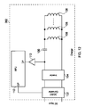
- FIG. 1 is a schematic diagram of system 1 .
- System 1 includes a primary unit (charger) 100 and a secondary unit (portable device, in this case) 200 .
- Primary unit 100 includes a DC/DC converter 102 , an inverter 104 , a capacitor (or capacitance) 106 , a primary coil 108 , a buffer 110 , and a microprocessor unit (MPU) 112 .
- Secondary unit 200 includes a secondary coil 202 , a capacitor (or capacitance) 204 , a rectifier 206 , a DC/DC converter 208 and a load 210 .
- Buffer 110 may be considered to be a peak detector, and may be employed to measure the peak voltage over the primary coil 108 .
- the primary unit 100 is configured to generate an electromagnetic field, and this field may be induced (as a horizontal or a vertical field, relative to a charging surface or power transfer surface of the primary unit) in proximity to the primary coil 108 . It will be appreciated that the configuration of the field is dependent on the configuration (i.e. physical layout) of the primary coil 108 .
- the electromagnetic field may be employed in the system 1 to transfer power to a secondary unit 200 requiring power located in proximity to the primary unit 100 .
- the primary unit 100 may have any suitable form, for example having a flat platform forming a power transfer surface on or in proximity to which the or each secondary unit 200 can be placed.
- the electromagnetic field may be distributed over a power transfer area of the surface, as described in GB-A-2388716, the entire contents of which are incorporated herein by reference. It will be appreciated that this form of primary unit may allow one or more secondary units 200 to be simultaneously located in proximity to the primary unit to receive power therefrom. It may be appreciated that many other forms of primary unit 100 may allow one or more secondary units 200 to be simultaneously located in proximity to the primary unit to receive power therefrom.
- Another possible form for primary unit 100 is a shelf, on which the secondary unit 200 can be placed to receive power. Such a form can be advantageous for allowing parts of the secondary device to sit outside the magnetic field.
- the secondary unit 200 in FIG. 1 is separable from the primary unit 100 and includes the secondary coil 202 which couples with the electromagnetic field generated by the primary unit 100 when the secondary unit 200 is in proximity to the primary unit 100 . In this way, power can be transferred inductively from the primary unit 100 to the secondary unit 200 without requiring direct electrically-conductive connections therebetween.
- the primary unit 100 is configured to provide the primary coil 108 with time-varying electrical signals, such as alternating signals.
- the primary coil 108 and the secondary coil 202 may have any suitable forms, but may for example be formed of copper wire wound around a high-permeability former, such as ferrite or amorphous metal.
- Litz wire is a particular type of wire which may be used in these circumstances. Litz wire has many strands of wire twisted together and can help reduce skin and proximity effects.
- the primary and secondary coils 108 , 202 may be different from one another, for example in size, number of turns, type of core, and physical layout etc. Multiple primary and secondary coils may be employed, and the number of primary and secondary coils may be different from one another.
- the secondary unit 200 is shown as a portable device, being an object requiring power.
- the portable device is shown as being the same as the secondary unit 200 , however the secondary unit 200 may be a component (for example, removable) part of the portable device.
- Load 210 may therefore be considered to be the actual load of the secondary unit 200 , although it could be separate or separable from the secondary unit 200 .
- the primary unit 100 of system 1 is shown as being a charger, operable to charge the portable device 200 by electromagnetic induction.
- the primary unit may more broadly be considered to be a wireless power supply. That is, the charging of a battery (or other energy storage cell) is merely one example application of such primary units.
- the secondary unit 200 may be considered to be only part of the device in FIG. 1 , for example only the secondary coil 202 , or the combination of the secondary coil 202 , capacitor 204 , rectifier 206 and DC/DC converter 208 .
- the secondary unit 200 may thus be connected to an external load (load 210 ), and may be configured to supply inductively-received power to the external load.
- the secondary unit 200 may be carried in or by an object requiring power (secondary device), such as a portable electrical or electronic device or a rechargeable battery or cell. Further information regarding possible designs of secondary unit 200 and the objects (secondary devices) that can be powered by the secondary unit 200 can be found in GB-A-2388716 (referred to above). In GB-A-2388716, such secondary units may be referred to as secondary devices.
- the secondary unit 200 is merely shown as a portable device to improve an understanding of the present invention.
- secondary units may be considered to be any electrical or electronic devices which require power, and may be portable such devices, for example (i.e. not exclusively) mobile phones, PDAs (Personal Digital Assistants), laptop computers, personal stereo equipment, MP3 players and the like, wireless headsets, vehicle charging units, home appliances such as kitchen appliances, personal cards such as credit cards, and wireless tags useful for tracking merchandise.
- PDAs Personal Digital Assistants
- laptop computers personal stereo equipment
- MP3 players Personal stereo equipment
- wireless headsets vehicle charging units
- home appliances such as kitchen appliances
- personal cards such as credit cards
- wireless tags useful for tracking merchandise.
- the DC/DC converter 102 is connected to receive an external DC input, and is operable to down-convert the received DC input to a lower DC voltage V d .
- the DC/DC converter 102 may be a switch-mode Buck converter for high efficiency.
- the DC/DC converter 102 is connected to drive the inverter 104 , which generates an AC voltage at its output.
- the inverter 104 may be a MOSFET half-bridge, driven from a reference oscillator (not shown).
- the AC voltage output by the inverter 104 is used to drive the primary inductive coil 108 .
- the capacitor 106 is connected in series with the primary coil, and the coil/capacitor combination is configured such that it is resonant at the operating frequency (the fundamental frequency) of the inverter 104 .
- the primary unit 100 may in some cases not have series resonant capacitor 106 .
- the peak coil voltage in the primary coil 108 , V pc is typically much larger than the DC voltage V d because the circuitry following the inverter (i.e. including primary coil 108 and capacitor 106 ) is configured to be resonant.
- the operating frequency may be considered constant or could be variable (i.e. tunable) for efficiency reasons. Indeed, the frequency could be tuned as a way of regulating the coil voltage (i.e. the magnitude of the electrical drive signals in the coil). For example, if the primary coil 108 is configured to be resonant, then it is possible to vary the magnitude of the drive signals by varying the frequency.
- the secondary coil 202 is connected to the input of the rectifier 206 in series with capacitor 204 , again such that the coil/capacitor combination is resonant.
- the secondary unit 200 may in some cases not have series resonant capacitor 204 .
- the secondary coil 202 presents the rectifier 206 with an AC voltage received via electromagnetic induction from the primary coil 108 .
- the rectifier 206 rectifies this AC voltage to output a DC voltage to the DC/DC converter 208 .
- the DC/DC converter 208 down-converts the rectified voltage from the coil to match the input voltage required by the load 210 .
- DC/DC converter 208 is, in some situations, preferably a switch-mode converter (similarly to converter 102 ) rather than a linear converter.
- a switch-mode converter is typically able to convert from one DC voltage to another DC voltage far more efficiently than a linear converter.
- a linear converter generally drops any excess voltage across a resistance. Therefore, the larger the difference between the input and output voltages, the lower the efficiency. This variation in efficiency with input voltage can render the power drawn by the secondary unit 200 of the system 1 not independent of input voltage, which can be undesirable.
- the DC/DC converter 208 of the secondary unit 200 is, optionally, configured to deliver a constant voltage to the load 210 .
- This constant voltage may be maintained by means of a feedback loop (not shown).
- the output voltage of the DC/DC converter 208 may be used to control the duty cycle of the DC/DC converter 208 in order to maintain the required input voltage, V load , of the load 210 irrespective of changes to the input voltage of the DC/DC converter 210 .
- the load 210 may change, e.g. if the load 210 is a battery having a charging cycle. Such batteries may have constant-current and constant-voltage portions of such a charging cycle, and thus it will be appreciated that at different times focus may be placed on current rather than voltage.
- the DC/DC converter 208 may be configured to maintain the required load voltage V load at different levels for the different parts of such a charging cycle.
- the required load voltage V load typically changes on a relatively slow timescale (minutes), such that over a short period of time (seconds) it appears to be relatively constant. There may however be “transients” occurring on a fast timescale (milliseconds), generally infrequently. Movement of the secondary unit, or some particular capability of the secondary unit (e.g. if it has RF functionality, such as in a mobile telephone), may cause such transients.
- the primary unit 100 of system 1 regulates the primary coil voltage V pc at a predetermined voltage level. This is achieved by means of a feedback loop including the buffer (peak detector) 110 and the microprocessor unit 112 . As shown in FIG. 1 , the primary coil voltage is essentially buffered by buffer 110 and input to the microprocessor unit (MPU) 112 . Based upon the primary coil voltage, the microprocessor unit 112 may control the duty cycle of the DC/DC converter 102 in order to maintain the predetermined level of primary coil voltage V pc irrespective of the load presented by the secondary unit 200 (and/or any other such presented load).
- MPU microprocessor unit
- the primary unit 100 of the system 1 may be configured to determine the amount of power drawn via the primary coil 108 , or the amount of current passing through the primary coil 108 , in addition to or instead of measuring the primary coil voltage V pc . That is, the regulation could be based on voltage, current or power measurements. For example, if power is considered, the primary unit 100 could be considered to measure both the voltage V d and the current drawn from the DC/DC converter 102 , I d . Measuring the voltage and current at this point has the advantage that the signals are DC. Within the microprocessor unit 112 , the signals concerned could be sampled using analogue-to-digital converters (ADCs) and low-pass filtered to reduce noise. Averaging may be used as part of this filtering. The values of the voltage V d and the current I d could then be, for example, determined within the microprocessor unit 112 and multiplied together to determine the power drawn.
- ADCs analogue-to-digital converters
- FIG. 2 is a schematic diagram of a system 300 according to one embodiment of the present invention.
- System 300 includes a primary unit 302 and a plurality of secondary units 200 .
- System 300 may therefore be useful for supplying power inductively to two or more secondary units 200 simultaneously (or one after the other, for example without having to swap one device for the other).
- FIG. 2 is presented at a circuitry level, and in this regard embodiments of the present invention focus on circuitry features. However, as well as relating to circuitry, the present invention extends to the primary unit itself (which may include features beyond the circuitry features shown, for example its physical structure) and to the overall power transfer system including such a primary unit.
- the secondary units 200 are shown as each including a secondary coil 202 but as representative of corresponding circuitry devices. This demonstrates that secondary units 200 may be only components of such secondary devices, and also enables a simplification of the schematic diagram. Thus, in one embodiment of the present invention, secondary units 200 may be the same as that in FIG. 1 . In another embodiment of the present invention, secondary units 200 in FIG. 2 (and in other Figures) may be different from that in FIG. 1 , and may be different from one another.
- Primary unit 302 differs from primary unit 100 in FIG. 1 , in that it includes a plurality of primary coils 108 .
- Primary coils 108 are connected together in parallel. Although three such primary coils are shown in FIG. 2 , it will be appreciated that two or more such coils could be provided and that the number of coils could be large, for example up to 10 or up to 50, or more.
- two of the primary coils 108 are shown as having a secondary unit 200 in proximity thereto, and the third primary coil 108 is shown as having no secondary unit 200 in proximity thereto.
- the primary coils 108 may have one or more secondary units 200 in proximity thereto, depending on the configuration of the primary coils 108 and the number of secondary units 200 requiring power.
- a primary coil (depending on its configuration) may simultaneously transfer power to more than one secondary unit.
- a secondary unit may receive power simultaneously from more than one primary coil in the same primary unit.
- the FIG. 2 embodiment is advantageous for the following reasons, at least.
- the primary unit 302 is provided with the capability of transferring power via a plurality of primary coils 108 without requiring a large replication in circuitry.
- the extra capability (as compared to the FIG. 1 system) is provided by adding extra primary coils 108 in parallel. In this way, minimum additional cost and complexity is incurred.
- embodiments providing the extra capability with low replication in the circuitry may require higher-rated (higher-power capability) components than embodiments in which lower-rated parts are replicated. In general, it may be less cost intensive to employ higher-rated components than to increase component count.
- the voltage over each of the primary coils 108 can be regulated without needing to provide additional circuitry, because the primary coil voltage V pc is the same for all of the parallel-connected primary coils 108 .
- V pc the primary coil voltage
- the control system is arranged such that it maintains all of the primary coils 108 at the same, regulated, voltage level.
- the FIG. 2 system is configured to operate when there are loads (secondary units/devices) in proximity to all of the primary coils 108 or only in proximity to some of the primary coils 108 .
- the FIG. 2 system is able to operate when there are different loads on different primary coils 108 .
- the regulation based on sensing the primary coil voltage V pc at a single point is satisfactory since the primary coils 108 are mutually parallel.
- the series capacitor 106 is provided in common to all of the primary coils 108 .
- the primary coils 108 are configured to be resonant at an intended frequency (i.e. tuned).
- the intended frequency may be the frequency at which the inverter 104 generates its alternating current (i.e. at the fundamental frequency of the alternating current).
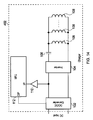
- FIG. 3 is a schematic diagram of a primary unit 306 according to one embodiment of the present invention.
- Primary unit 306 may, for example, be used interchangeably with primary unit 302 in the FIG. 2 embodiment.
- Primary unit 306 differs from primary unit 302 , in that a ballast circuit 308 is provided. In addition, it is more clearly apparent from FIG. 3 that any number of primary coils 108 may be provided in parallel with one another.
- Ballast circuit 308 is provided between the inverter 104 , and the capacitor 106 and coil 108 combination.
- Ballast circuit 308 includes an inductor 310 and capacitor 312 . Accordingly, ballast circuit 308 may be referred to as an LC ballast circuit.
- Inductor 308 is connected in series between the inverter 104 and the capacitor 106 .
- Capacitor 312 is connected in parallel with the capacitor 106 and coil 108 combination.
- the ballast circuit 308 is advantageous as it acts as a low-pass filter and reduces the magnitude of harmonics present in signals on the primary coils 108 . This may help to reduce or avoid the generation by the primary unit 306 of unwanted radio-frequency interference and electromagnetic interference.
- ballast circuit 308 in the primary unit 306 can also be advantageous from the point of view of stability of operation of the primary unit and in terms of regulating operation of the primary unit. This can be true both when the primary unit has a single primary coil 108 and when the primary unit has a plurality of primary coils. Such a ballast circuit may be configured advantageously to improve system stability by appropriate selection of component values. Advantages relating to the ballast circuit 308 will now be considered further.
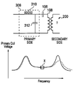
- FIG. 4 presents a set of schematic diagrams useful for understanding the benefit of a ballast circuit in a primary unit of an inductive power transfer system.
- FIG. 4A is a schematic diagram representative of parts of the system of FIG. 2 . It is assumed that the primary side is supplied with a fixed alternating current such that the primary coil 108 generates an electromagnetic field to transfer power inductively to the secondary side. It is also assumed that characteristics of the secondary side are unknown, for example the load in the secondary unit, the number of secondary units present, etc. It is also assumed that no regulation of the signals in the primary coil 108 is provided. Importantly, no ballast circuit is present in the FIG. 4A circuitry.
- FIG. 4B is a schematic representation of the frequency response of the circuitry in the primary side of FIG. 4A .
- the solid curve indicates that the FIG. 4A circuitry may have a resonant response with a single main peak.
- the curves shown with dashed lines are to represent ways in which the resonant response could change with the changing secondary side (e.g. changing load, number of secondary units, etc).
- the slope of the curve could change either side of the resonant peak or the peak frequency could change, or indeed a combination of those changes could occur.
- FIG. 4C is a schematic diagram representative of parts of the system of FIG. 3 .
- the primary side is supplied with a fixed alternating current such that the primary coil 108 generates an electromagnetic field to transfer power inductively to the secondary side.
- characteristics of the secondary side are unknown, for example the load in the secondary unit, the number of secondary units present, etc.
- ballast circuit 308 is present in the circuitry.
- FIG. 4D is a schematic representation of the frequency response of the circuitry in the primary side of FIG. 4C .
- the solid curve indicates that the FIG. 4C circuitry may be configured to have a resonant response with two main peaks, joined by a relatively flat portion.
- the curve shown with a dashed line is to represent a way in which the resonant response could change with the changing secondary side (e.g. changing load, number of secondary units, etc).
- the substantially flat central portion (marked with the box labelled “X” in FIG. 4D ) experiences little, if any, change.
- the changing frequency response with changing secondary side adds little or no substantial burden in the primary side if it is desired to regulate, for example, the voltage over the primary coil.
- the primary side is desensitized to changes on the secondary side.
- FIG. 5 is a schematic diagram akin to that in FIG. 4C , i.e. of a system according to one embodiment of the present invention in which the primary side has a ballast circuit.
- the schematic diagram has been used to simulate operation of the system, to demonstrate the benefits of the ballast circuitry.
- the circuitry further includes the primary coil 108 (pad inductor, L pad or L p ) and capacitor 106 (series resonant cap, C p ), which are also tuned to f 0 .
- Frequency f 0 is chosen as the switching frequency of the inverter 104 for the present simulations, which frequency is typically in the range 100-500 kHz for wireless power transfer applications.
- primary core 108 pad inductor, L pad
- the additional labels in FIG. 5 are designators for the simulations.
- the inductor 310 (ballast) and capacitor 312 (tank) are driven by a constant AC voltage (provided from inverter 104 ) and can effectively act as a constant current source or be used to provide a constant coil voltage. This is effectively independent of small component tolerances, since (as mentioned above) operation is carried out in the flat region of the frequency-response curve, between the two main resonant peaks.
- FIG. 6 is a graph of simulation results based on the FIG. 5 circuitry.
- FIG. 6 is a frequency response curve obtained using the parameter values set out below it.
- the labelling of the parameters corresponds to the labelling in FIG. 5 .
- the frequency of operation was chosen to be 323 kHz (0.323 MHz).
- the frequency response was found to be much as shown in FIG. 4D , i.e. with two main resonant peaks with a substantially flat portion therebetween.
- the frequency of operation 323 kHz, was chosen to be in the centre of the curve between the two main peaks, where the curve is substantially flat.
- the solid-line curve shows the response when no secondary unit is present, and the dashed-line curve shows the response when the secondary-side is present and operating at full power. As can be seen, the operating point in the curve (in the flat portion) does not noticeably change between these two situations.
- each pair of components i.e. the inductor 310 and capacitor 312 as one pair and the capacitor 106 and primary coil 108 as another pair, tuned to the same frequency f 0 (by suitable selection of their inductance and capacitance values), as this maintains the same basic resonant curve shapes.
- increasing the ratio (“the inductor ratio”) of the inductance of the ballast inductor 308 to the inductance of the primary core 108 i.e. L bal /L pad
- moves the resonant peaks further apart in frequency and lowering the inductance of the ballast inductor 308 increases the current in the primary coil (the pad current).
- the resonant peaks are located as follows:
- ⁇ peak is the peak angular frequency (in radians)
- ⁇ 0 is the operating angular frequency (in radians)
- L bal is the inductance of ballast inductor 310
- L pad is the inductance of the primary coil 108 .
- the current in the primary coil 108 is approximately given by:
- Ipad Vinp ⁇ 0 ⁇ Lbal
- V inp the peak magnitude of the input alternating voltage as shown in FIG. 5 .
- the peak voltage over the primary coil is approximately given by:
- Vpad Vinp ⁇ Lpad Lbal
- V inp is the magnitude of the fundamental frequency (sinusoidal component at f 0 ) generated by inverter 104 . This may be considered to be equal to the inverter rail voltage multiplied by 2/ ⁇ .
- FIG. 7 is a graph of simulation results showing the effect of the inductor ratio on the separation between the resonant peaks.
- the y-axis represents the separation between the peaks in frequency, divided by the centre frequency.
- the centre frequency is at the centre of the x-axis in FIG. 6 .
- FIG. 8 is a graph of simulation results showing the effect of the inductance value of the ballast inductor 310 on the current (the primary current) in the primary coil 108 .
- an example design process for designing circuitry as in FIG. 5 might be, in one embodiment of the present invention, as follows:
- Step 3 the expected voltage over the primary coil(s) 108 is thus approximately:
- Vpad Vinp ⁇ Lpad Lbal
- the number of turns in the primary coil may be selected to work with practical inverter voltages, primary-coil voltages and primary-coil currents. Selection of inverter and coil voltages is typically affected by available FETs, efficiency requirements, cost and EMC (electromagnetic compatability) considerations. Design trade-offs may mean that the ratio selected in step 2 is adjusted accordingly.
- Step 4 if appropriate, carry out fine-tuning of the overall design.
- the resonant frequency of the ballast inductor 310 and tank capacitor 312 pair may be adjusted slightly to allow zero-voltage switching to be used by the inverter FETs under all tolerance conditions.
- ZVS zero-voltage switching
- the primary coil has a self-inductance, L pad or L p , which is the reactance of the coil in isolation (neglecting parasitics such as inter-winding capacitance).
- L pad or L p the reactance of the coil in isolation
- the effective inductance may appear different and may be modified depending on the inductance of the secondary coil, L s , the degree of coupling between the two coils and the impedance of the load imposed by the secondary unit.
- the effective inductance seen may be different to the measured inductance in isolation.
- the effective inductance may vary depending on how strong the coupling is and may therefore be dependent on how closely aligned the primary and secondary coils are.
- FIG. 9 is a schematic diagram of a system 350 according to one embodiment of the present invention.
- System 350 similarly to system 300 , includes a primary unit 352 and a plurality of secondary units 200 .
- Primary unit 352 is generally the same as primary unit 306 , except that only two primary coils 108 are shown, and except that a specific example implementation of primary coil 108 is shown.
- Each primary coil 108 in primary unit 352 includes a bar-shaped piece of ferrite acting as a primary core 109 with turns of the corresponding primary coil 108 wound around it and distributed along its length.
- the secondary coils 202 in the secondary units 200 of system 350 also have a similar configuration. That is, the secondary coil 202 in each secondary unit 200 of FIG. 9 includes a bar-shaped piece of ferrite acting as a secondary core 203 with turns of the corresponding secondary coil 202 wound around it and distributed along its length.
- the secondary coils 202 (and cores 203 ) are of slightly smaller dimensions than the primary coils 108 (and cores 109 ), giving some freedom of placement in the positioning of the device.
- the primary coils 108 could be the same size as (or slightly smaller than) the secondary coils.
- the primary coils 108 are physically arranged such that they share a common coil axis, however they are arranged so that adjacent such primary coils have opposite polarities to each other. This is exemplified in FIG. 9 by the coil ends of the two shown primary coils 108 that are adjacent to one another being connected together in common and similarly the furthest-apart ends being connected together in common.
- An advantage of this layout is that the far-field electromagnetic field generated by the primary coils 108 may be cancelled to some extent, which can reduce interference caused by the primary unit 352 . In this fashion, a larger number of primary coils 108 can be provided in a line with alternate polarities.
- the primary coils 108 could be arranged in a different manner, for example side-by-side.
- the primary coils may all have the same polarity, or the opposing polarities may be provided from separate out-of-phase driving systems.
- the arrangement of the primary coils 108 in the present embodiment lends itself to the shelf format of the primary unit mentioned above.
- the line of primary coils 108 could sit under the shelf, rendering the shelf itself as a power transfer surface.
- Secondary units 200 could then be arranged on the shelf to receive power inductively therefrom.
- FIG. 10 is a schematic diagram of a primary unit 362 according to one embodiment of the present invention.
- the number of primary coils 108 provided in primary units presented herein may vary from embodiment to embodiment.
- primary unit 362 may, for example, be used interchangeably with primary units 302 , 306 and 352 .
- Primary unit 362 differs from primary unit 306 , as follows. Firstly, the circuitry portion including ballast circuit 308 , capacitor 106 and one of the primary coils 108 is repeated per primary coil 108 , and those portions are connected together in parallel. Secondly, the buffer 110 (peak detector) is only connected to one of the primary coils 108 .
- the ballast circuits are all connected to the inverter 104 , such that inverter 104 drives them all simultaneously.
- This configuration of the primary unit 362 takes advantage of the benefits of the ballast circuit 308 discussed in detail above. That is, the inverter 104 is configured such that its fundamental output frequency is in the substantially flat portion of the frequency response curve for each of the parallel-connected portions.
- the parallel-connected portions By configuring the parallel-connected portions such that they are mutually-similar to one another, it can be arranged that the substantially flat portion of the frequency response curve for each of the parallel-connected portions lies in approximately the same place in frequency. Therefore, the overall combination of the parallel-connected portions (and each such portion individually) is desensitized to changes on the secondary side (e.g.
- FIG. 11 is a schematic diagram of a primary unit 372 according to one embodiment of the present invention.
- Primary unit 372 may, for example, be used interchangeably with primary units 302 , 306 , 352 , and 362 .
- Primary unit 372 is generally the same as primary unit 362 except that each primary coil 108 is provided with a feedback path via a buffer 110 (peak detector). Further, an MPU 374 with multiple inputs is provided instead of MPU 112 .
- Primary unit 372 is operable to sense the voltage over each of the primary coils 108 and to regulate its operation, in this case by controlling operation of DC/DC converter 102 , in dependence upon any one or more of those sensed voltages. In certain circumstances, for example when only one secondary unit 200 is present, it can be advantageous to control regulation based upon the sensed voltage from a particular primary coil 108 , for accuracy of control of that particular coil. In other circumstances, it may be advantageous to base regulation on the voltages over a different coil 108 at different times. Overall, a high capability in control is afforded in primary unit 372 .
- FIGS. 12 to 15 present schematic diagrams of primary units 382 , 392 , 402 and 412 , respectively, each forming a different embodiment of the present invention.
- Each of these primary units may, for example, may be used interchangeably with any of the primary units 302 , 306 , 352 , 362 and 372 .
- Each of the primary units 382 , 392 , 402 and 412 is generally the same as primary unit 302 , except for the following differences. It will be appreciated that these embodiments are intended to demonstrate that the feedback signal (sensing operation of the circuitry) may be obtained at any of several different points in the primary-unit circuitry.
- an AC voltage sense is provided as in primary unit 302 but from between the capacitor 106 and the inverter 104 .
- an AC current sensor 394 is provided at the primary coils (represented as a current transformer).
- a DC voltage sense is provided between the DC/DC converter 102 and the inverter 104 .
- a DC current sense (formed by a series resistor 414 and an operational amplifier 416 ) is provided between the DC/DC converter 102 and the inverter 104 .
- FIG. 16 is a schematic diagram of a primary unit 422 according to one embodiment of the present invention.
- Primary unit 422 may, for example, be used interchangeably with any of primary units 302 , 306 , 352 , 362 , 372 , 382 , 392 , 402 and 412 .
- Primary unit 422 is generally similar to primary unit 372 , except that the parallel portions do not have ballast circuits (but another embodiment could include such ballast circuits), and that the capacitors 106 in each parallel portion are replaced with variable reactances (variable capacitors) 424 . Further, primary unit 422 has an MPU 426 (instead of MPU 112 ) which has an input per voltage sense (via buffers 110 ) and an output per variable reactance 424 so as to control the value of those reactances.
- each parallel portion has a primary coil 108 and variable reactance 424 connected together in series.
- Each variable reactance 424 is implemented in this embodiment as a variable capacitor, formed by an array of capacitors which may be switched in or out under control of the MPU 426 .
- the variable capacitors may be fabricated using MOSFETs or MEMs by way of example. The value of the variable capacitors is controllable by the MPU 426 .
- the LC combination (of the primary coil 108 and variable reactance 424 ) is tuned such that the combination may be brought in or out of resonance.
- the peak coil voltage concerned may be controllably varied, based upon tuning the resonant frequency of the LC combination towards or away from the fundamental frequency of the inverter 104 .
- each primary coil 108 may be regulated at a different voltage level. It will be understood that although embodiments disclosed herein focus on voltage sensing and regulation, other embodiments of the present invention may regulate current or power in the primary coils 108 .
- each of the primary coils 108 it is not essential for each of the primary coils 108 to have a variable reactance 424 .
- one of the primary coils 108 could have a fixed capacitor, such as capacitor 106 , and the others could have variable reactances.
- the primary coils 108 could be regulated together by controlling the DC/DC converter 102 , and the primary coils 108 could be regulated relative to one another (and the coil 108 with the fixed capacitor 106 ) by controlling the variable reactances 424 .
- a variable impedance could be employed (incorporating a resistance), however the losses associated with the resistances (manifested as heat dissipation) may be undesirable in some embodiments.
- FIG. 17 is a schematic diagram of a primary unit 432 according to one embodiment of the present invention.
- primary unit 432 may be used interchangeably with previously-described primary units embodying the present invention.
- Primary unit 432 is the same as primary unit 422 , except that instead of the parallel portions being driven by common inverter 104 , each such portion is driven by a half-bridge 434 , with the half-bridges 434 being driven by a common driver 436 and oscillator 438 .
- variable capacitor there are several ways of forming the variable capacitor (e.g. using varactors or various series and parallel combinations of capacitor).
- a fixed capacitor in series with a variable inductance could be used, since varying L or C will vary the overall LC combination.
- This could be realised with a switched array of individual conductors, or, for instance, by providing a coil wound around a ferrite rod, with taps in the coil, such that different sets of turns can be shorted or selected to alter the overall inductance.
- FIG. 18 is a schematic diagram of a primary unit 442 according to one embodiment of the present invention.
- primary unit 442 may be used interchangeably with previously-described primary units embodying the present invention.
- Primary unit 442 is closely similar to primary unit 432 , except that each parallel portion is provided with its own inverter 104 instead of the half-bridges 434 (and driver 436 and oscillator 438 ). Further, each of the variable reactances 424 is replaced with a fixed capacitor 106 .
- each inverter is provided with its own tunable oscillator 444 controllable by the MPU 426 .
- the driving frequency i.e. the fundamental output frequency of the inverter 104 concerned
- each primary coil 108 can be adjusted to bring it towards or away from resonance, thereby adjusting the AC voltage (peak voltage or, for example RMS voltage) across it.
- the signal on each primary coil is sensed via a buffer (peak detector) 110 , and the MPU 426 is operable to dynamically control the signals on its outputs to perform system control/regulation.
- the MPU 426 may selectively control operation of the DC/DC converter 102 and/or the operation of one ore more of the tunable oscillators 444 .
- the MPU 426 is operable to dynamically regulate the voltage (or current or power, in other embodiments) in each of the primary coils 108 , either all to the same level or to different levels, as desired.
- each of the inverters 104 it is not necessary for each of the inverters 104 to be provided with its own tunable oscillator 444 .
- one of the inverters 104 could be provided with a fixed-frequency oscillator, and the others could have tunable oscillators 444 .
- the primary coils 108 could be regulated together by controlling the DC/DC converter 102 , and the primary coils 108 could be regulated relative to one another (and to the coil 108 with the fixed-frequency oscillator) by controlling the tunable oscillators 444 .
- FIGS. 19 and 20 are schematic diagrams of possible primary coil 108 layouts on the charging surfaces of primary units according to some embodiments of the present invention.
- a secondary unit 200 could be placed anywhere, or substantially anywhere, on such charging surfaces of primary units to be charged.
- the primary unit concerned may include a plurality of primary coils.
- the charging surface has an array of wound ferrite coils 450 , i.e. an array of wound coils 450 on a ferrite back-plate 452 .
- the charging surface has an array of printed hexagonal spiral coils 460 etched on to a PCB (printed circuit board) 462 , which may have a ferrite and/or metal shield underneath.
- each hexagonal arrangement 460 may be considered to be an individual coil.
- Rectangles 464 represent the possible footprints of a secondary unit 200 , or a secondary device incorporating such a secondary unit, placed on the charging surface of the primary unit concerned to be charged (i.e. to receive power inductively therefrom).
- the footprint of the secondary unit 200 may be smaller than the charging area on the charging surface, such that multiple secondary units may be charged at the same time.
- arrays such as those shown in FIGS. 19 and 20 , it may be possible to switch primary coils 108 in and out, so that only certain coils are active at a particular time. When one primary coil 108 is switched out, it may be desirable to switch in an inductor (a dummy coil) instead, to retain the same overall inductance and keep the system on resonance. This concept could be applied by analogy to any of the previously described embodiments to form new embodiments of the present invention, and this concept is explored in more detail later herein.
- This concept may also be advantageous even if only a single secondary unit is receiving power, as different primary coils and even different numbers of primary coils may need to be active depending on the position and/or orientation of the secondary unit with respect to the charging surface. Therefore, depending on such position/orientation, different dummy coils or different numbers of dummy coils may need to be active at different times to maintain system resonance.
- the “dummy coils” may be standard inductors, which may be smaller and lighter than primary coils. Further, they may be shielded or designed not to radiate so as not to affect the electromagnetic field generated by the primary coils.
- the dummy coils may be located in the primary unit away from the power transfer area so as to minimise any effect from them (heat, radiation, or otherwise). Thus, it may be possible to maintain the inductance seen from the driving circuitry using dummy coils, without those dummy coils affecting the electromagnetic field generated.
- FIG. 21 is a schematic diagram of a primary unit 472 according to one embodiment of the present invention.
- primary unit 472 may be used interchangeably with any of the previously-described primary units embodying the present invention.
- the “dummy coil” concept could be applied to any of the previously-described embodiments, and primary unit 472 is one example of this concept as applied to primary unit 306 of FIG. 3 .
- each of the primary coils 108 is provided in series with a switch 474 , so that it may be switched (for example under control of the MPU 112 ) in or out.
- switches 474 In parallel with the primary coils 108 (and switches 474 ) there are provided corresponding inductors 476 (acting as dummy coils) connected in series with switches 478 .
- an inductor (dummy coil) 476 may be switched in, in order to maintain the same overall inductance of the parallel arrangement of primary coils 108 and inductors 476 .
- FIG. 22 is a schematic diagram of a primary unit 482 representing a number of embodiments of the present invention.
- Primary unit 482 is intended to generically demonstrate how the concept of switching in and out primary coils 108 and inductors (dummy coils) 476 can be applied to embodiments of the present invention.
- Primary unit 482 includes an array of primary coils 108 and inductors 476 , a driver 484 and a switch unit 486 .
- the primary coils 108 and inductors 476 are commonly connected at one end via the switch unit 486 to a ground terminal in the driver 484 .
- the other end of each of the primary coils 108 and inductors 476 is selectively connectable under control of the switch unit 486 to either output 1 or output 2 of the driver 484 .
- the driver 484 could have any number of outputs, and only two are shown for convenience.
- the configuration of primary unit 482 is generally applicable to primary-unit embodiments disclosed herein.
- the primary coils 108 could be the array in FIG. 19 or 20 .
- the primary coils 108 and inductors 476 could be those in FIG. 21
- the switch unit 486 could be the combination of switches of 474 and 478 in FIG. 21
- the driver 484 could be the remaining parts of the circuitry in FIG. 21 , with the driver output being between the capacitor 106 and buffer 110 in FIG. 21 .
- the benefit of providing more than one output in the driver 484 is that the primary coils 108 and inductors 476 can be controlled in sets, one set per output, such that (for example) one set could be regulated at a different voltage to another. As exemplified in FIG. 22 , any number of the primary coils 108 and inductors 476 could be connected to any of the driver outputs.
- FIG. 23 is a schematic diagram of a driver 492 which may be interchanged with driver 484 to form an embodiment of the present invention.
- driver 492 is the same as primary unit 492 of FIG. 23 , except that the primary coils 108 have been removed leaving outputs 1 and 2 , and that the remaining lower outputs of the half-bridges 434 are connected together in common for compatibility with the common ground in FIG. 22 . Accordingly, it is understood that one set of primary coils 108 (or inductors 476 ) may be regulated at one voltage (via output 1 ), and another set of primary coils 108 (or inductors 476 ) may be regulated at another voltage (via output 2 ). Again, as before, regulation could be voltage, current or power regulation.
- Having different primary coils 108 regulated to different primary-coil voltages can be useful for supplying different levels of power to different loads (e.g. different types of secondary unit 200 or secondary device) which are on the same charging surface, or, at least, receiving power inductively from the same primary unit.
- loads e.g. different types of secondary unit 200 or secondary device
- This can also be useful because the coupling between primary unit and secondary unit can vary widely depending on the position and/or orientation of the secondary unit relative to the primary unit.
- tolerances in practical capacitors and inductors can result in differences from one secondary unit or device to the next.
- the primary and secondary units could be configured to communicate with one another.
- a secondary device in one embodiment of the present invention could be configured to communicate to the primary unit information indicative of its power of requirement.
- the primary unit could be configured to regulate the relevant primary coils accordingly. It will be recognised that in some embodiments such communication may only need to be one-way communication, for example from secondary unit to primary unit, although more robust communication may take advantage of two-way communication.
- FIG. 24 is a schematic diagram of a primary unit 502 according to one embodiment of the present invention.
- Primary unit 502 is an example implementation of primary unit 582 , in which banks of primary coils 108 and inductors (dummy coils) 476 are shown separately (as in FIG. 21 ) and in which an example implementation of switch unit 486 is explicitly shown. Further, it is shown that control of the switch unit 486 could be handled by an MPU 504 , which may be part of or separate from the MPUs shown in the other embodiments of the present invention disclosed herein.
- a primary unit could potentially drive a primary coil or coils for one secondary unit at one frequency and a different primary coil or coils for a different secondary unit at a different frequency in dependence upon feedback signals from those secondary units.
- some embodiments may obtain feedback signals from the secondary side (as well as, or instead as, feedback signals from the primary side).
Abstract
Description
-
- A primary unit having at least one primary coil, through which it drives an alternating current, creating a time-varying magnetic flux.
- A secondary unit, separable from the primary unit, having a secondary coil.
where ωpeak is the peak angular frequency (in radians), ω0 is the operating angular frequency (in radians), i.e. the centre-frequency of the response curve, Lbal is the inductance of
where Vinp is the peak magnitude of the input alternating voltage as shown in
Claims (22)
Priority Applications (2)
| Application Number | Priority Date | Filing Date | Title |
|---|---|---|---|
| US13/209,584 US8884469B2 (en) | 2007-12-21 | 2011-08-15 | Circuitry for inductive power transfer |
| US14/510,554 US9906047B2 (en) | 2007-12-21 | 2014-10-09 | Circuitry for inductive power transfer |
Applications Claiming Priority (7)
| Application Number | Priority Date | Filing Date | Title |
|---|---|---|---|
| GB0724981.6 | 2007-12-21 | ||
| GB0724981A GB0724981D0 (en) | 2007-12-21 | 2007-12-21 | Enhanced power supply |
| GB0724982.4 | 2007-12-21 | ||
| GB0724982A GB0724982D0 (en) | 2007-12-21 | 2007-12-21 | Inductive power supply |
| PCT/GB2008/004206 WO2009081126A1 (en) | 2007-12-21 | 2008-12-18 | Circuitry for inductive power transfer |
| US80849010A | 2010-12-13 | 2010-12-13 | |
| US13/209,584 US8884469B2 (en) | 2007-12-21 | 2011-08-15 | Circuitry for inductive power transfer |
Related Parent Applications (3)
| Application Number | Title | Priority Date | Filing Date |
|---|---|---|---|
| PCT/GB2008/004206 Continuation WO2009081126A1 (en) | 2007-12-21 | 2008-12-18 | Circuitry for inductive power transfer |
| US12/808,490 Continuation US8884468B2 (en) | 2007-12-21 | 2008-12-18 | Circuitry for inductive power transfer |
| US80849010A Continuation | 2007-12-21 | 2010-12-13 |
Related Child Applications (1)
| Application Number | Title | Priority Date | Filing Date |
|---|---|---|---|
| US14/510,554 Continuation US9906047B2 (en) | 2007-12-21 | 2014-10-09 | Circuitry for inductive power transfer |
Publications (2)
| Publication Number | Publication Date |
|---|---|
| US20110291491A1 US20110291491A1 (en) | 2011-12-01 |
| US8884469B2 true US8884469B2 (en) | 2014-11-11 |
Family
ID=40430486
Family Applications (6)
| Application Number | Title | Priority Date | Filing Date |
|---|---|---|---|
| US12/809,119 Active 2031-07-13 US8766487B2 (en) | 2007-12-21 | 2008-12-18 | Inductive power transfer |
| US12/808,490 Active 2032-02-09 US8884468B2 (en) | 2007-12-21 | 2008-12-18 | Circuitry for inductive power transfer |
| US13/209,584 Active 2030-06-13 US8884469B2 (en) | 2007-12-21 | 2011-08-15 | Circuitry for inductive power transfer |
| US14/278,683 Active 2029-02-13 US9906044B2 (en) | 2007-12-21 | 2014-05-15 | Inductive power transfer |
| US14/510,554 Active 2030-06-10 US9906047B2 (en) | 2007-12-21 | 2014-10-09 | Circuitry for inductive power transfer |
| US15/903,695 Active 2029-02-21 US10763699B2 (en) | 2007-12-21 | 2018-02-23 | Inductive power transfer |
Family Applications Before (2)
| Application Number | Title | Priority Date | Filing Date |
|---|---|---|---|
| US12/809,119 Active 2031-07-13 US8766487B2 (en) | 2007-12-21 | 2008-12-18 | Inductive power transfer |
| US12/808,490 Active 2032-02-09 US8884468B2 (en) | 2007-12-21 | 2008-12-18 | Circuitry for inductive power transfer |
Family Applications After (3)
| Application Number | Title | Priority Date | Filing Date |
|---|---|---|---|
| US14/278,683 Active 2029-02-13 US9906044B2 (en) | 2007-12-21 | 2014-05-15 | Inductive power transfer |
| US14/510,554 Active 2030-06-10 US9906047B2 (en) | 2007-12-21 | 2014-10-09 | Circuitry for inductive power transfer |
| US15/903,695 Active 2029-02-21 US10763699B2 (en) | 2007-12-21 | 2018-02-23 | Inductive power transfer |
Country Status (12)
| Country | Link |
|---|---|
| US (6) | US8766487B2 (en) |
| EP (3) | EP2232668A1 (en) |
| JP (2) | JP5426570B2 (en) |
| KR (3) | KR101645736B1 (en) |
| CN (3) | CN101981780A (en) |
| AU (2) | AU2008339681A1 (en) |
| CA (2) | CA2709867C (en) |
| HK (1) | HK1150903A1 (en) |
| MY (1) | MY154347A (en) |
| RU (2) | RU2517435C2 (en) |
| TW (3) | TWI508408B (en) |
| WO (2) | WO2009081126A1 (en) |
Cited By (18)
| Publication number | Priority date | Publication date | Assignee | Title |
|---|---|---|---|---|
| US20140054970A1 (en) * | 2012-08-24 | 2014-02-27 | Qualcomm Incorporated | System and method for power output control in wireless power transfer systems |
| US9114719B1 (en) | 2010-06-02 | 2015-08-25 | Bryan Marc Failing | Increasing vehicle security |
| US20150291042A1 (en) * | 2012-08-31 | 2015-10-15 | Siemens Aktiengesellschaft | Battery charging system and method for cableless charging of a battery |
| US9537353B1 (en) | 2014-06-03 | 2017-01-03 | Apple Inc. | Methods for detecting mated coils |
| US9685814B1 (en) | 2014-06-13 | 2017-06-20 | Apple Inc. | Detection of coil coupling in an inductive charging system |
| US9750923B2 (en) | 2014-11-19 | 2017-09-05 | Velóce Corporation | Wireless communications system integrating electronics into orally ingestible products for controlled release of active ingredients |
| US9813041B1 (en) | 2014-07-31 | 2017-11-07 | Apple Inc. | Automatic boost control for resonant coupled coils |
| US9923383B2 (en) | 2014-02-23 | 2018-03-20 | Apple Inc. | Adjusting filter in a coupled coil system |
| US10014733B2 (en) | 2014-08-28 | 2018-07-03 | Apple Inc. | Temperature management in a wireless energy transfer system |
| US10028238B2 (en) | 2014-12-05 | 2018-07-17 | Mitsubishi Electric Engineering Company, Limited | Resonance type power transmission system, transmitting device, and power supply position control system |
| US10032557B1 (en) | 2014-05-29 | 2018-07-24 | Apple Inc. | Tuning of primary and secondary resonant frequency for improved efficiency of inductive power transfer |
| US10116279B2 (en) | 2014-02-23 | 2018-10-30 | Apple Inc. | Impedance matching for inductive power transfer systems |
| US10193372B2 (en) | 2014-09-02 | 2019-01-29 | Apple Inc. | Operating an inductive energy transfer system |
| US10389274B2 (en) | 2017-04-07 | 2019-08-20 | Apple Inc. | Boosted output inverter for electronic devices |
| US10523063B2 (en) | 2017-04-07 | 2019-12-31 | Apple Inc. | Common mode noise compensation in wireless power systems |
| US10644531B1 (en) | 2016-09-22 | 2020-05-05 | Apple Inc. | Adaptable power rectifier for wireless charger system |
| US10666084B2 (en) | 2015-07-10 | 2020-05-26 | Apple Inc. | Detection and notification of an unpowered releasable charging device |
| US10819154B2 (en) | 2016-09-06 | 2020-10-27 | Apple Inc. | Inductive power transmitter |
Families Citing this family (413)
| Publication number | Priority date | Publication date | Assignee | Title |
|---|---|---|---|---|
| GB2414120B (en) | 2004-05-11 | 2008-04-02 | Splashpower Ltd | Controlling inductive power transfer systems |
| GB2414121B (en) | 2004-05-11 | 2008-04-02 | Splashpower Ltd | Controlling inductive power transfer systems |
| MY154347A (en) | 2007-12-21 | 2015-05-29 | Access Business Group Int Llc | Circuitry for inductive power transfer |
| JP2009169327A (en) * | 2008-01-21 | 2009-07-30 | Hitachi Displays Ltd | Power transmission circuit |
| US8855554B2 (en) * | 2008-03-05 | 2014-10-07 | Qualcomm Incorporated | Packaging and details of a wireless power device |
| US8234509B2 (en) * | 2008-09-26 | 2012-07-31 | Hewlett-Packard Development Company, L.P. | Portable power supply device for mobile computing devices |
| US20110074346A1 (en) * | 2009-09-25 | 2011-03-31 | Hall Katherine L | Vehicle charger safety system and method |
| JP5258521B2 (en) * | 2008-11-14 | 2013-08-07 | トヨタ自動車株式会社 | Power supply system |
| KR20110103408A (en) * | 2009-01-08 | 2011-09-20 | 엔이씨 도낀 가부시끼가이샤 | Electric power transmitting apparatus and noncontact electric power transmission system |
| US8497658B2 (en) | 2009-01-22 | 2013-07-30 | Qualcomm Incorporated | Adaptive power control for wireless charging of devices |
| US9407327B2 (en) * | 2009-02-13 | 2016-08-02 | Qualcomm Incorporated | Wireless power for chargeable and charging devices |
| JP5621203B2 (en) * | 2009-03-30 | 2014-11-12 | 富士通株式会社 | Wireless power supply system and wireless power supply method |
| JP5353376B2 (en) * | 2009-03-31 | 2013-11-27 | 富士通株式会社 | Wireless power device and wireless power receiving method |
| US8536736B2 (en) * | 2009-04-03 | 2013-09-17 | International Business Machines Corporation | Wireless power infrastructure |
| US9231411B2 (en) * | 2009-04-08 | 2016-01-05 | Access Business Group International Llc | Selectable coil array |
| JP5431774B2 (en) * | 2009-04-14 | 2014-03-05 | 富士通テン株式会社 | Wireless power transmission apparatus and wireless power transmission method |
| EP2433347B1 (en) * | 2009-05-20 | 2013-10-23 | Koninklijke Philips N.V. | Electronic device having an inductive receiver coil with ultra-thin shielding layer and method |
| US8655272B2 (en) * | 2009-07-07 | 2014-02-18 | Nokia Corporation | Wireless charging coil filtering |
| DE102009033236A1 (en) * | 2009-07-14 | 2011-01-20 | Conductix-Wampfler Ag | Device for inductive transmission of electrical energy |
| DE102009033239C5 (en) | 2009-07-14 | 2023-05-17 | Conductix-Wampfler Gmbh | Device for the inductive transmission of electrical energy |
| DE102009033237A1 (en) * | 2009-07-14 | 2011-01-20 | Conductix-Wampfler Ag | Device for inductive transmission of electrical energy |
| CA2768397A1 (en) | 2009-07-24 | 2011-01-27 | Access Business Group International Llc | Power supply |
| EP2293411B1 (en) * | 2009-09-03 | 2021-12-15 | TDK Corporation | Wireless power feeder and wireless power transmission system |
| US8575944B2 (en) | 2009-11-03 | 2013-11-05 | Robert Bosch Gmbh | Foreign object detection in inductive coupled devices |
| US8952617B2 (en) * | 2009-11-03 | 2015-02-10 | City University Of Hong Kong | Passive LC ballast and method of manufacturing a passive LC ballast |
| DE102009057437B4 (en) * | 2009-12-09 | 2023-03-16 | Sew-Eurodrive Gmbh & Co Kg | Arrangement for inductive charging of an energy storage vehicle and charging station |
| US9154002B2 (en) | 2010-01-25 | 2015-10-06 | Access Business Group International Llc | Systems and methods for detecting data communication over a wireless power link |
| KR101928904B1 (en) * | 2010-02-08 | 2018-12-14 | 필립스 아이피 벤쳐스 비.브이. | A method of calibrating a parasitic metal detection system and a method of collecting calibration data for a parasitic metal detection system |
| AU2011224345A1 (en) * | 2010-03-10 | 2012-11-01 | Witricity Corporation | Wireless energy transfer converters |
| US9106086B2 (en) * | 2010-03-11 | 2015-08-11 | Qualcomm Incorporated | Detection and protection of devices within a wireless power system |
| DE102010012356B4 (en) | 2010-03-22 | 2021-04-29 | Sew-Eurodrive Gmbh & Co Kg | System for contactless energy transfer to a vehicle |
| JP2011211760A (en) * | 2010-03-26 | 2011-10-20 | Panasonic Electric Works Co Ltd | Contactless power supply device and contactless charging system |
| US9561730B2 (en) * | 2010-04-08 | 2017-02-07 | Qualcomm Incorporated | Wireless power transmission in electric vehicles |
| US10343535B2 (en) | 2010-04-08 | 2019-07-09 | Witricity Corporation | Wireless power antenna alignment adjustment system for vehicles |
| KR101142446B1 (en) * | 2010-05-04 | 2012-05-11 | 국민대학교산학협력단 | wireless power transmission device with a tunable impedance matching circuit |
| JP2011250615A (en) * | 2010-05-28 | 2011-12-08 | Nec Tokin Corp | Non-contact power transmission and communication system |
| TWI473381B (en) * | 2011-09-20 | 2015-02-11 | Fu Da Tong Technology Co Ltd | Induction power supply system and intruding metal detection method thereof |
| US9413197B2 (en) | 2010-05-31 | 2016-08-09 | Fu Da Tong Technology Co., Ltd. | Inductive power supply system and intruding metal detection method thereof |
| JP2012016125A (en) * | 2010-06-30 | 2012-01-19 | Panasonic Electric Works Co Ltd | Non-contact power supply system, and metal foreign substance detector of non-contact power supply system |
| EP2591535A2 (en) | 2010-07-07 | 2013-05-15 | Robert Bosch GmbH | Foreign object detection in inductive coupled wireless power transfer environment using thermal sensors |
| DE102010026780A1 (en) | 2010-07-09 | 2012-01-12 | Audi Ag | Measuring a temperature during contactless transmission of energy |
| JP5736991B2 (en) * | 2010-07-22 | 2015-06-17 | Tdk株式会社 | Wireless power supply apparatus and wireless power transmission system |
| TWI451238B (en) * | 2010-07-28 | 2014-09-01 | Mstar Semiconductor Inc | Power control apparatus and method thereof and mobile apparatus using it |
| WO2012021070A1 (en) * | 2010-08-10 | 2012-02-16 | Powerbyproxi Limited | A magnetic shield |
| JP2012044735A (en) * | 2010-08-13 | 2012-03-01 | Sony Corp | Wireless charging system |
| JP5664015B2 (en) * | 2010-08-23 | 2015-02-04 | Tdk株式会社 | Coil device and non-contact power transmission device |
| KR101782354B1 (en) | 2010-08-30 | 2017-09-27 | 삼성전자주식회사 | Apparatus and method for resonant power transmission and resonant power reception |
| JP2012049434A (en) * | 2010-08-30 | 2012-03-08 | Sony Corp | Electronic component, feeder device, power receiver, and wireless feeder system |
| US9294153B2 (en) * | 2010-09-23 | 2016-03-22 | Texas Instruments Incorporated | Systems and methods of wireless power transfer with interference detection |
| NZ588159A (en) * | 2010-09-23 | 2014-01-31 | Powerbyproxi Ltd | A contactless power transfer system |
| DE102010043154A1 (en) * | 2010-10-29 | 2012-05-03 | Fraunhofer-Gesellschaft zur Förderung der angewandten Forschung e.V. | Portable electronic device, external base device, method for coupling the portable electronic device to an external base device and use of the external base device for coupling the portable electronic device |
| US9219378B2 (en) * | 2010-11-01 | 2015-12-22 | Qualcomm Incorporated | Wireless charging of devices |
| KR101213086B1 (en) * | 2010-11-04 | 2012-12-18 | 유한회사 한림포스텍 | Method for controlling wireless power signal in wireless power transmission device and wireless power transmission using the same |
| TWI435511B (en) * | 2010-12-06 | 2014-04-21 | Asustek Comp Inc | Wireless charging system and transmission circuit thereof |
| US20120146424A1 (en) * | 2010-12-14 | 2012-06-14 | Takashi Urano | Wireless power feeder and wireless power transmission system |
| US9058928B2 (en) | 2010-12-14 | 2015-06-16 | Tdk Corporation | Wireless power feeder and wireless power transmission system |
| DE102010054472A1 (en) * | 2010-12-14 | 2012-06-14 | Conductix-Wampfler Ag | Device for inductive transmission of electrical energy |
| KR101750415B1 (en) | 2010-12-16 | 2017-06-26 | 삼성전자주식회사 | Protector of rectifier, Wireless power receiving apparatus including the protector |
| US8800738B2 (en) * | 2010-12-28 | 2014-08-12 | Tdk Corporation | Wireless power feeder and wireless power receiver |
| US9088307B2 (en) * | 2010-12-29 | 2015-07-21 | National Semiconductor Corporation | Non-resonant and quasi-resonant system for wireless power transmission to multiple receivers |
| US9628147B2 (en) | 2011-02-01 | 2017-04-18 | Fu Da Tong Technology Co., Ltd. | Method of automatically adjusting determination voltage and voltage adjusting device thereof |
| US9600021B2 (en) | 2011-02-01 | 2017-03-21 | Fu Da Tong Technology Co., Ltd. | Operating clock synchronization adjusting method for induction type power supply system |
| TWI568125B (en) | 2015-01-14 | 2017-01-21 | 富達通科技股份有限公司 | Supplying-end module of induction type power supply system and voltage measurement method thereof |
| US9671444B2 (en) | 2011-02-01 | 2017-06-06 | Fu Da Tong Technology Co., Ltd. | Current signal sensing method for supplying-end module of induction type power supply system |
| US10056944B2 (en) | 2011-02-01 | 2018-08-21 | Fu Da Tong Technology Co., Ltd. | Data determination method for supplying-end module of induction type power supply system and related supplying-end module |
| US10038338B2 (en) | 2011-02-01 | 2018-07-31 | Fu Da Tong Technology Co., Ltd. | Signal modulation method and signal rectification and modulation device |
| US10615645B2 (en) | 2011-02-01 | 2020-04-07 | Fu Da Tong Technology Co., Ltd | Power supply device of induction type power supply system and NFC device identification method of the same |
| US10630113B2 (en) | 2011-02-01 | 2020-04-21 | Fu Da Tong Technology Co., Ltd | Power supply device of induction type power supply system and RF magnetic card identification method of the same |
| US10289142B2 (en) | 2011-02-01 | 2019-05-14 | Fu Da Tong Technology Co., Ltd. | Induction type power supply system and intruding metal detection method thereof |
| TWI570427B (en) | 2015-10-28 | 2017-02-11 | 富達通科技股份有限公司 | Induction type power supply system and intruding metal detection method thereof |
| US10312748B2 (en) | 2011-02-01 | 2019-06-04 | Fu Da Tong Techology Co., Ltd. | Signal analysis method and circuit |
| US9831687B2 (en) | 2011-02-01 | 2017-11-28 | Fu Da Tong Technology Co., Ltd. | Supplying-end module for induction-type power supply system and signal analysis circuit therein |
| JP5713714B2 (en) * | 2011-02-10 | 2015-05-07 | キヤノン株式会社 | Power supply apparatus and control method |
| US9118357B2 (en) | 2011-02-17 | 2015-08-25 | Qualcomm Incorporated | Systems and methods for controlling output power of a wireless power transmitter |
| KR101243587B1 (en) * | 2011-02-17 | 2013-03-20 | 주식회사 팬택 | Non-contract charging device, non-contact charghing system and non-contact charging method |
| JP5751858B2 (en) * | 2011-02-22 | 2015-07-22 | キヤノン株式会社 | Power supply apparatus and control method |
| JP5805408B2 (en) * | 2011-03-10 | 2015-11-04 | 株式会社レゾナント・システムズ | Bus digital wireless microphone system |
| WO2012138949A2 (en) | 2011-04-08 | 2012-10-11 | Access Business Group International Llc | Counter wound inductive power supply |
| US9912201B2 (en) * | 2011-04-11 | 2018-03-06 | Texas Instruments Incorporated | Systems and methods of detecting a change in object presence in a magnetic field |
| KR102017106B1 (en) * | 2011-05-17 | 2019-10-21 | 삼성전자주식회사 | Power transmitting device and method of transmitting power for communicating with one or more power receiving devices |
| US9735623B2 (en) | 2011-05-17 | 2017-08-15 | Samsung Electronics Co., Ltd. | Power transmitting method and power transmitter for communication with power receiver |
| DE102011076186A1 (en) * | 2011-05-20 | 2012-11-22 | Siemens Aktiengesellschaft | Arrangement and method for eliminating a disturbance of a wireless energy transmission |
| DE102011050655A1 (en) | 2011-05-26 | 2012-11-29 | Conductix-Wampfler Gmbh | Method for detecting an electrically conductive foreign body and device for inductive transmission of electrical energy |
| DE202011050264U1 (en) | 2011-05-26 | 2012-08-27 | Conductix-Wampfler Gmbh | Device for inductive transmission of electrical energy |
| JP6067211B2 (en) * | 2011-05-27 | 2017-01-25 | 日産自動車株式会社 | Non-contact power feeding device |
| US20120313577A1 (en) * | 2011-06-10 | 2012-12-13 | Access Business Group International Llc | System and method for detecting, characterizing, and tracking an inductive power receiver |
| DE102011105063B4 (en) * | 2011-06-21 | 2023-09-21 | Airbus Operations Gmbh | Detection of a foreign body in an inductive transmission path |
| US9300147B2 (en) * | 2011-06-29 | 2016-03-29 | Lg Electronics Inc. | Method for avoiding signal collision in wireless power transfer |
| JP5071574B1 (en) * | 2011-07-05 | 2012-11-14 | ソニー株式会社 | Sensing device, power receiving device, non-contact power transmission system, and sensing method |
| JP5899490B2 (en) * | 2011-07-20 | 2016-04-06 | パナソニックIpマネジメント株式会社 | Contactless power supply system |
| CA2844062C (en) * | 2011-08-04 | 2017-03-28 | Witricity Corporation | Tunable wireless power architectures |
| WO2013022255A2 (en) * | 2011-08-09 | 2013-02-14 | 주식회사 케이더파워 | High efficiency wireless charger |
| TWI425738B (en) * | 2011-08-12 | 2014-02-01 | 富達通科技股份有限公司 | Induction charging method |
| KR101880030B1 (en) | 2011-08-25 | 2018-07-23 | 삼성전자주식회사 | Sauce apparatus and method that control magnetic field using two sauce resonators in Wireless Resonant Power Transfer system |
| US8909149B2 (en) * | 2011-08-26 | 2014-12-09 | Hewlett-Packard Development Company, L.P. | Media module of a device |
| EP2566028B1 (en) * | 2011-09-05 | 2014-07-09 | RRC power solutions GmbH | Switching assembly and method for inductive energy transfer |
| EP2566005A1 (en) * | 2011-09-05 | 2013-03-06 | RRC power solutions GmbH | Switching assembly and method for inductive energy transfer |
| JP5940784B2 (en) * | 2011-09-09 | 2016-06-29 | 国立大学法人埼玉大学 | Non-contact power feeding device for moving objects |
| US9252846B2 (en) | 2011-09-09 | 2016-02-02 | Qualcomm Incorporated | Systems and methods for detecting and identifying a wireless power device |
| CN103875159B (en) | 2011-09-09 | 2017-03-08 | WiTricity公司 | Exterior object detection in wireless energy transmission system |
| JP5794056B2 (en) | 2011-09-12 | 2015-10-14 | ソニー株式会社 | Power supply device and power supply system |
| US20130062966A1 (en) | 2011-09-12 | 2013-03-14 | Witricity Corporation | Reconfigurable control architectures and algorithms for electric vehicle wireless energy transfer systems |
| JP5842106B2 (en) * | 2011-09-20 | 2016-01-13 | パナソニックIpマネジメント株式会社 | Contactless power supply system |
| US9553485B2 (en) | 2011-10-13 | 2017-01-24 | Integrated Device Technology, Inc. | Apparatus, system, and method for detecting a foreign object in an inductive wireless power transfer system based on input power |
| US9450648B2 (en) | 2011-10-13 | 2016-09-20 | Integrated Device Technology, Inc. | Apparatus, system, and method for detecting a foreign object in an inductive wireless power transfer system |
| WO2013057896A1 (en) | 2011-10-18 | 2013-04-25 | 株式会社アドバンテスト | Wireless power receiving apparatus, wireless power supplying apparatus, and wireless power supplying system |
| CA2794161A1 (en) * | 2011-11-03 | 2013-05-03 | Shaw Industries Group, Inc. | Wireless energy transfer systems |
| US9118203B2 (en) | 2011-11-15 | 2015-08-25 | Qualcomm Incorporated | Systems and methods for induction charging with a closed magnetic loop |
| CN103124083A (en) * | 2011-11-18 | 2013-05-29 | 深圳富泰宏精密工业有限公司 | Wireless charging type portable type electronic device and matched charging device |
| JP5842161B2 (en) * | 2011-11-22 | 2016-01-13 | パナソニックIpマネジメント株式会社 | Lighting apparatus and visible light communication system using the same |
| DE102011086904A1 (en) * | 2011-11-23 | 2013-05-23 | Robert Bosch Gmbh | Device and method for inductive energy transmission |
| JP5838768B2 (en) * | 2011-11-30 | 2016-01-06 | ソニー株式会社 | Sensing device, power receiving device, non-contact power transmission system, and sensing method |
| JP6099019B2 (en) | 2011-12-14 | 2017-03-22 | パナソニックIpマネジメント株式会社 | Non-contact connector device and system |
| US9041254B2 (en) * | 2011-12-14 | 2015-05-26 | Linear Technology Corporation | Primary unit control of resonant inductive power transfer system for optimum efficiency |
| CN103348561B (en) * | 2011-12-14 | 2017-07-07 | 松下知识产权经营株式会社 | The information transmission system |
| US9806537B2 (en) | 2011-12-15 | 2017-10-31 | Samsung Electronics Co., Ltd | Apparatus and method for determining whether a power receiver is removed from the apparatus |
| CN104272545B (en) * | 2011-12-16 | 2018-06-12 | 奥克兰联合服务有限公司 | Inductive power transfer systems and method |
| DE102011088911A1 (en) * | 2011-12-16 | 2013-06-20 | Robert Bosch Gmbh | Object recognition with wireless energy transmission |
| KR102023068B1 (en) * | 2011-12-22 | 2019-09-20 | 지이 하이브리드 테크놀로지스, 엘엘씨 | Wireless power transmitting device and method for controlling to transmit wireless power signal in wireless power transmitting device |
| JP6019581B2 (en) * | 2011-12-26 | 2016-11-02 | ソニー株式会社 | Detection device, detection system, power transmission device, non-contact power transmission system, and detection method |
| US8868813B2 (en) | 2011-12-30 | 2014-10-21 | Bedrock Automation Platforms Inc. | Communications control system with a serial communications interface and a parallel communications interface |
| US10834094B2 (en) | 2013-08-06 | 2020-11-10 | Bedrock Automation Platforms Inc. | Operator action authentication in an industrial control system |
| US8971072B2 (en) * | 2011-12-30 | 2015-03-03 | Bedrock Automation Platforms Inc. | Electromagnetic connector for an industrial control system |
| US8862802B2 (en) * | 2011-12-30 | 2014-10-14 | Bedrock Automation Platforms Inc. | Switch fabric having a serial communications interface and a parallel communications interface |
| US9467297B2 (en) | 2013-08-06 | 2016-10-11 | Bedrock Automation Platforms Inc. | Industrial control system redundant communications/control modules authentication |
| US11144630B2 (en) | 2011-12-30 | 2021-10-12 | Bedrock Automation Platforms Inc. | Image capture devices for a secure industrial control system |
| US11967839B2 (en) | 2011-12-30 | 2024-04-23 | Analog Devices, Inc. | Electromagnetic connector for an industrial control system |
| US11314854B2 (en) | 2011-12-30 | 2022-04-26 | Bedrock Automation Platforms Inc. | Image capture devices for a secure industrial control system |
| US10834820B2 (en) | 2013-08-06 | 2020-11-10 | Bedrock Automation Platforms Inc. | Industrial control system cable |
| US9600434B1 (en) | 2011-12-30 | 2017-03-21 | Bedrock Automation Platforms, Inc. | Switch fabric having a serial communications interface and a parallel communications interface |
| US9437967B2 (en) | 2011-12-30 | 2016-09-06 | Bedrock Automation Platforms, Inc. | Electromagnetic connector for an industrial control system |
| US9727511B2 (en) | 2011-12-30 | 2017-08-08 | Bedrock Automation Platforms Inc. | Input/output module with multi-channel switching capability |
| US9191203B2 (en) | 2013-08-06 | 2015-11-17 | Bedrock Automation Platforms Inc. | Secure industrial control system |
| KR102014126B1 (en) * | 2012-01-06 | 2019-08-26 | 필립스 아이피 벤쳐스 비.브이. | Wireless power receiver system |
| JP6090172B2 (en) * | 2012-01-17 | 2017-03-08 | パナソニックIpマネジメント株式会社 | Contactless charging method |
| US9417199B2 (en) * | 2012-01-17 | 2016-08-16 | Triune Systems, LLC | Method and system of wireless power transfer foreign object detection |
| US10778045B2 (en) | 2012-01-30 | 2020-09-15 | Triune Ip, Llc | Method and system of wireless power transfer foreign object detection |
| JP2013158589A (en) * | 2012-02-08 | 2013-08-19 | Toshiba Corp | Medical image diagnosis apparatus |
| KR101305828B1 (en) * | 2012-03-07 | 2013-09-06 | 엘지이노텍 주식회사 | Apparatus for transmitting wireless power, apparatus for receiving wireless power, system for transmitting wireless power and method for transmitting wireless power |
| KR101360744B1 (en) * | 2012-02-17 | 2014-02-10 | 엘지이노텍 주식회사 | Apparatus for transmitting wireless power, apparatus for receiving wireless power, system for transmitting wireless power and method for transmitting wireless power |
| TWI587597B (en) | 2012-02-17 | 2017-06-11 | Lg伊諾特股份有限公司 | Wireless power transmitter, wireless power receiver, and power transmission method of wireless power transmitting system |
| JP2013183497A (en) * | 2012-02-29 | 2013-09-12 | Equos Research Co Ltd | Power transmission system |
| JP2013183496A (en) * | 2012-02-29 | 2013-09-12 | Equos Research Co Ltd | Power transmission system |
| DE112012005961A5 (en) * | 2012-02-29 | 2014-12-11 | Siemens Aktiengesellschaft | Charging system for the galvanically isolated charging of an electrical energy storage device of a vehicle, electrically driven vehicle, charging station for a vehicle and corresponding method |
| JP5909700B2 (en) | 2012-03-09 | 2016-04-27 | パナソニックIpマネジメント株式会社 | Metal detection method, metal detection device, and metal detection method and non-contact power supply device of non-contact power supply device |
| JP5903624B2 (en) * | 2012-03-09 | 2016-04-13 | パナソニックIpマネジメント株式会社 | Non-contact power transmission device driving method and non-contact power transmission device |
| FR2988241B1 (en) * | 2012-03-13 | 2019-08-09 | Renault S.A.S | WIRELESS COMMUNICATION SYSTEM WITH MULTIPLE MULTIPLEX RECEIVERS. |
| US9895988B2 (en) * | 2012-03-14 | 2018-02-20 | Panasonic Intellectual Property Management Co., Ltd. | Electricity supply device, electricity reception device, and electricity supply system |
| US20130257167A1 (en) * | 2012-03-29 | 2013-10-03 | Integrated Device Technology, Inc. | Apparatuses, systems, and methods for power transfer adjustment in wireless power transfer systems |
| US8942624B2 (en) | 2012-03-30 | 2015-01-27 | Integrated Device Technology, Inc. | Apparatus, system, and method for back-channel communication in an inductive wireless power transfer system |
| CN102607727A (en) * | 2012-04-05 | 2012-07-25 | 杭州凯源电子有限公司 | Radio-frequency temperature measuring device with function of resonance isolation electricity-taking |
| JP5966538B2 (en) * | 2012-04-10 | 2016-08-10 | ソニー株式会社 | Power receiving device, power receiving device control method, and power feeding system |
| KR101844422B1 (en) | 2012-04-19 | 2018-04-03 | 삼성전자주식회사 | Apparatus and method for wireless energy transmission and apparatus wireless energy reception |
| KR101890705B1 (en) | 2012-04-19 | 2018-08-22 | 삼성전자주식회사 | Signal process apparatus and signal process method |
| JP5872374B2 (en) * | 2012-04-25 | 2016-03-01 | 三洋電機株式会社 | Contactless power supply method |
| US9696358B2 (en) | 2012-05-02 | 2017-07-04 | Powerbyproxi Limited | Method for detecting and identifying a receiver in an inductive power transfer system |
| EP2845290B1 (en) | 2012-05-03 | 2018-08-29 | Powermat Technologies Ltd. | System and method for triggering power transfer across an inductive power coupling and non resonant transmission |
| JP5976385B2 (en) * | 2012-05-07 | 2016-08-23 | ソニー株式会社 | Detecting device, power receiving device, power transmitting device, and non-contact power feeding system |
| US9536656B2 (en) | 2012-05-21 | 2017-01-03 | Texas Instruments Incorporated | Systems and methods of reduction of parasitic losses in a wireless power system |
| DE202013012728U1 (en) | 2012-06-22 | 2019-01-08 | Sony Corporation | processing device |
| JP5915904B2 (en) * | 2012-06-22 | 2016-05-11 | ソニー株式会社 | Processing apparatus, processing method, and program |
| DE102012210897A1 (en) * | 2012-06-26 | 2014-01-02 | Robert Bosch Gmbh | Object recognition for an energy transmission system |
| KR101338690B1 (en) * | 2012-07-06 | 2013-12-09 | 홍익대학교 산학협력단 | Method and apparatus for adaptive impedance matching of wireless power transfer |
| KR101950688B1 (en) | 2012-07-09 | 2019-02-21 | 삼성전자주식회사 | Wireless power transmitter and method for controlling thereof |
| KR102074475B1 (en) | 2012-07-10 | 2020-02-06 | 지이 하이브리드 테크놀로지스, 엘엘씨 | Apparatus and method for detecting foreign object in wireless power transmitting system |
| US9467002B2 (en) | 2012-07-19 | 2016-10-11 | Ford Global Technologies, Llc | Vehicle charging system |
| US20140021912A1 (en) * | 2012-07-19 | 2014-01-23 | Ford Global Technologies, Llc | Vehicle battery charging system and method |
| US10773596B2 (en) | 2012-07-19 | 2020-09-15 | Ford Global Technologies, Llc | Vehicle battery charging system and method |
| KR101413490B1 (en) * | 2012-07-24 | 2014-07-01 | (주)기술과가치 | Wiress Power Transmission Apparatus and Method for Constructing Wiress Charging Space Using the Same |
| EP2878061B1 (en) | 2012-07-27 | 2023-10-25 | Tc1 Llc | Thermal management for implantable wireless power transfer systems |
| JP5974710B2 (en) * | 2012-07-27 | 2016-08-23 | 株式会社Ihi | Foreign matter removal mechanism |
| WO2014018971A1 (en) * | 2012-07-27 | 2014-01-30 | Thoratec Corporation | Resonant power transfer systems with protective algorithm |
| US10383990B2 (en) * | 2012-07-27 | 2019-08-20 | Tc1 Llc | Variable capacitor for resonant power transfer systems |
| WO2014018969A2 (en) | 2012-07-27 | 2014-01-30 | Thoratec Corporation | Resonant power transfer system and method of estimating system state |
| WO2014018972A1 (en) | 2012-07-27 | 2014-01-30 | Thoratec Corporation | Computer modeling for resonant power transfer systems |
| US9805863B2 (en) | 2012-07-27 | 2017-10-31 | Thoratec Corporation | Magnetic power transmission utilizing phased transmitter coil arrays and phased receiver coil arrays |
| WO2014018967A1 (en) | 2012-07-27 | 2014-01-30 | Thoratec Corporation | Self-tuning resonant power transfer systems |
| WO2014018973A1 (en) | 2012-07-27 | 2014-01-30 | Thoratec Corporation | Resonant power transmission coils and systems |
| US9722462B2 (en) * | 2012-08-03 | 2017-08-01 | Mediatek Singapore Pte. Ltd. | System and method for controlling resonant wireless power source |
| DE102012213958A1 (en) * | 2012-08-07 | 2014-05-22 | Bayerische Motoren Werke Aktiengesellschaft | Foreign body monitoring in inductive charging |
| US9154189B2 (en) * | 2012-08-17 | 2015-10-06 | Qualcomm Incorporated | Wireless power system with capacitive proximity sensing |
| DE102012215376A1 (en) * | 2012-08-30 | 2014-05-28 | Bayerische Motoren Werke Aktiengesellschaft | Foreign body detection in inductive charging |
| JP5988210B2 (en) * | 2012-08-31 | 2016-09-07 | 株式会社エクォス・リサーチ | Power transmission system |
| EP2891218A4 (en) * | 2012-08-31 | 2016-05-18 | Auckland Uniservices Ltd | Improved efficiency non-self tuning wireless power transfer systems |
| JP6061375B2 (en) * | 2012-09-06 | 2017-01-18 | Necトーキン株式会社 | Contactless power transmission device and contactless charging system |
| DE102012108671A1 (en) * | 2012-09-17 | 2014-05-28 | Paul Vahle Gmbh & Co. Kg | Metal foreign object detection system for inductive power transmission systems |
| WO2014045571A1 (en) * | 2012-09-18 | 2014-03-27 | Panasonic Corporation | Contactless electric power feeding system |
| US9178361B2 (en) * | 2012-09-27 | 2015-11-03 | ConvenientPower, Ltd. | Methods and systems for detecting foreign objects in a wireless charging system |
| US9190876B2 (en) * | 2012-09-28 | 2015-11-17 | Qualcomm Incorporated | Systems and methods for detecting wireless charging transmit characteristics |
| JP5988211B2 (en) * | 2012-09-28 | 2016-09-07 | 株式会社エクォス・リサーチ | Power transmission system |
| US10404075B2 (en) * | 2012-09-28 | 2019-09-03 | Avago Technologies International Sales Pte. Limited | Power receiving device having device discovery and power transfer capabilities |
| US9601930B2 (en) * | 2012-09-28 | 2017-03-21 | Broadcom Corporation | Power transmitting device having device discovery and power transfer capabilities |
| FR2996372B1 (en) * | 2012-10-01 | 2015-05-15 | Renault Sa | NON-CONTACT CHARGING SYSTEM OF A MOTOR VEHICLE BATTERY |
| TW201415749A (en) * | 2012-10-12 | 2014-04-16 | Espower Electronics Inc | Wireless power supply system for supporting multi remote devices |
| US9716388B2 (en) * | 2012-10-16 | 2017-07-25 | Koninklijke Philips N.V. | Wireless inductive power transfer |
| CN109969007A (en) | 2012-10-19 | 2019-07-05 | 韦特里西提公司 | External analyte detection in wireless energy transfer system |
| US9376026B2 (en) | 2012-10-19 | 2016-06-28 | Qualcomm Incorporated | System and method for inductance compensation in wireless power transfer |
| CN102904180B (en) * | 2012-10-24 | 2016-09-21 | 国网四川省电力公司绵阳供电公司 | Heat dissipation control device of switch cabinet |
| US9368269B2 (en) | 2012-10-24 | 2016-06-14 | Schumacher Electric Corporation | Hybrid battery charger |
| GB2507533A (en) * | 2012-11-02 | 2014-05-07 | Bombardier Transp Gmbh | Inductive power receiver having compensating arrangement |
| KR20210096686A (en) | 2012-11-05 | 2021-08-05 | 애플 인크. | Inductively coupled power transfer systems |
| KR102008810B1 (en) * | 2012-11-12 | 2019-08-08 | 엘지이노텍 주식회사 | Wireless power transmitting apparatus and method |
| FR2998412B1 (en) * | 2012-11-19 | 2014-12-26 | Continental Automotive France | METHOD FOR SEARCHING FOR THE PRESENCE OF A PARASITE OBJECT FOR A MAGNETIC INDUCTION POWER TRANSMITTING UNIT |
| US9793740B2 (en) | 2012-11-26 | 2017-10-17 | Samsung Electronics Co., Ltd. | Apparatus and method for charge control in wireless charging system |
| JP5983363B2 (en) * | 2012-11-30 | 2016-08-31 | 株式会社デンソー | Contactless power supply |
| GB2508924A (en) | 2012-12-17 | 2014-06-18 | Bombardier Transp Gmbh | Inductive power transfer system having array of sensing capacitors |
| GB2508923A (en) | 2012-12-17 | 2014-06-18 | Bombardier Transp Gmbh | Inductive power transfer system having inductive sensing array |
| CN103023160A (en) * | 2012-12-19 | 2013-04-03 | 哈尔滨工业大学 | Wireless power supply system used for printed circuit boards |
| JP6420025B2 (en) * | 2013-03-08 | 2018-11-07 | マクセルホールディングス株式会社 | Non-contact power transmission apparatus and non-contact power transmission method |
| WO2014119389A1 (en) * | 2013-01-31 | 2014-08-07 | 日立マクセル株式会社 | Contactless power transmission system and contactless power transmission method |
| JP6172956B2 (en) * | 2013-01-31 | 2017-08-02 | 日立マクセル株式会社 | Non-contact power transmission apparatus and non-contact power transmission method |
| FR3002099B1 (en) * | 2013-02-12 | 2016-05-27 | Proton World Int Nv | CONFIGURING NFC ROUTERS FOR P2P COMMUNICATION |
| JP2014155375A (en) * | 2013-02-12 | 2014-08-25 | Nitto Denko Corp | Wireless power transmission device, supply power control method of wireless power transmission device and manufacturing method of wireless power transmission device |
| KR102053462B1 (en) | 2013-02-14 | 2019-12-06 | 지이 하이브리드 테크놀로지스, 엘엘씨 | Apparatus and method for detecting foreign object in wireless power transmitting system |
| CN105075062B (en) | 2013-02-19 | 2017-11-14 | 松下知识产权经营株式会社 | Detection device for foreign matter, foreign matter detecting method and non-contact charger systems |
| KR102049118B1 (en) | 2013-02-20 | 2020-01-08 | 지이 하이브리드 테크놀로지스, 엘엘씨 | Apparatus and method for detecting foreign object in wireless power transmitting system |
| TWI482389B (en) * | 2013-03-01 | 2015-04-21 | Luxx Lighting Technology Taiwan Ltd | Inductive power transfer system, and transmitter and receiver devices thereof |
| KR102015496B1 (en) * | 2013-03-04 | 2019-08-28 | 엘지전자 주식회사 | Electronic device, electronic vechicle, wireless power transfer apparatus |
| JP6132266B2 (en) * | 2013-03-05 | 2017-05-24 | パナソニックIpマネジメント株式会社 | Non-contact power feeding device |
| US9680310B2 (en) | 2013-03-15 | 2017-06-13 | Thoratec Corporation | Integrated implantable TETS housing including fins and coil loops |
| US9502910B2 (en) | 2013-03-15 | 2016-11-22 | Samsung Electro-Mechanics Co., Ltd. | Power charging apparatus and battery apparatus |
| WO2014145895A1 (en) | 2013-03-15 | 2014-09-18 | Thoratec Corporation | Malleable tets coil with improved anatomical fit |
| KR102044807B1 (en) | 2013-03-18 | 2019-11-15 | 삼성전자주식회사 | Wireless power transmission control apparatus and wireless power transmission control method |
| JP5808355B2 (en) * | 2013-03-22 | 2015-11-10 | 株式会社東芝 | Wireless power feeding system, power reception control device, and power transmission control device |
| KR101482841B1 (en) * | 2013-03-29 | 2015-01-21 | 가천대학교 산학협력단 | Microchip using wireless induction heating and drug delivery device comprising the same |
| KR102340579B1 (en) * | 2013-05-15 | 2021-12-21 | 지이 하이브리드 테크놀로지스, 엘엘씨 | Multimedia system implementing wireless charge function installed in vehicle, method for replaying multimedia file using the same, and wireless power transmission device used therein |
| WO2015015495A1 (en) * | 2013-07-30 | 2015-02-05 | Powermat Technologies Ltd. | Efficiency monitor for inductive power transmission |
| US10613567B2 (en) | 2013-08-06 | 2020-04-07 | Bedrock Automation Platforms Inc. | Secure power supply for an industrial control system |
| CN105518970B (en) * | 2013-08-06 | 2018-10-26 | 联发科技(新加坡)私人有限公司 | Wireless power source with parallel resonance power source path |
| KR101875974B1 (en) * | 2013-08-14 | 2018-07-06 | 엘지이노텍 주식회사 | A wireless power transmission apparatus and method thereof |
| US9929601B2 (en) | 2013-08-23 | 2018-03-27 | Qualcomm Incorporated | Apparatus and method for lost power detection |
| JP6387222B2 (en) * | 2013-08-28 | 2018-09-05 | ソニー株式会社 | Power feeding device, power receiving device, power feeding system, and method for controlling power feeding device |
| US9882437B2 (en) * | 2013-08-28 | 2018-01-30 | Sony Corporation | Power feeding apparatus, power receiving apparatus, power feeding system, and method of controlling power feeding |
| DE202014011252U1 (en) | 2013-08-28 | 2018-11-06 | Sony Corporation | Power feeding device, power receiving device and power feeding system |
| US9425640B2 (en) * | 2013-09-26 | 2016-08-23 | The Charles Stark Draper Laboratory, Inc. | System and method of inductive charging and localization through using multiple primary inductive coils to detect the induced voltage of a secondary inductive coil |
| DE102013219538A1 (en) * | 2013-09-27 | 2015-04-02 | Siemens Aktiengesellschaft | Charging station for an electrically driven vehicle |
| US9921045B2 (en) | 2013-10-22 | 2018-03-20 | Qualcomm Incorporated | Systems, methods, and apparatus for increased foreign object detection loop array sensitivity |
| DE102013221659A1 (en) | 2013-10-24 | 2015-04-30 | Siemens Aktiengesellschaft | Arrangement for providing an inductive charging connection |
| WO2015070205A1 (en) | 2013-11-11 | 2015-05-14 | Thoratec Corporation | Resonant power transfer systems with communications |
| US10695476B2 (en) | 2013-11-11 | 2020-06-30 | Tc1 Llc | Resonant power transfer systems with communications |
| EP3069358B1 (en) | 2013-11-11 | 2019-06-12 | Tc1 Llc | Hinged resonant power transfer coil |
| KR102154306B1 (en) * | 2013-11-15 | 2020-09-10 | 지이 하이브리드 테크놀로지스, 엘엘씨 | Wireless power transmission device which enables to simultaneously charge |
| TWI489729B (en) * | 2013-11-18 | 2015-06-21 | Richtek Technology Corp | Power calculating method adopted in wireless power system |
| WO2015072565A1 (en) * | 2013-11-18 | 2015-05-21 | 株式会社Ihi | Wireless power supply system |
| CN103595109B (en) * | 2013-12-03 | 2016-03-30 | 东南大学 | A kind of electric automobile mobile charging method and apparatus |
| EP3086440B1 (en) * | 2013-12-05 | 2021-02-03 | Panasonic Intellectual Property Management Co., Ltd. | Array coil system |
| US10090718B2 (en) * | 2013-12-16 | 2018-10-02 | Panasonic Intellectual Property Management Co., Ltd. | Contactless charging device, program therefor, and automobile having contactless charging device mounted therein |
| US10381950B2 (en) | 2014-02-19 | 2019-08-13 | New York University | Resonant inverter topology, wireless charger, and control method |
| RU2649905C2 (en) * | 2014-02-25 | 2018-04-05 | Ниссан Мотор Ко., Лтд. | Wireless power feeding system and power transmission device |
| US10610692B2 (en) | 2014-03-06 | 2020-04-07 | Tc1 Llc | Electrical connectors for implantable devices |
| US9716861B1 (en) | 2014-03-07 | 2017-07-25 | Steelcase Inc. | Method and system for facilitating collaboration sessions |
| US10664772B1 (en) | 2014-03-07 | 2020-05-26 | Steelcase Inc. | Method and system for facilitating collaboration sessions |
| KR102187437B1 (en) * | 2014-03-11 | 2020-12-08 | 엘지이노텍 주식회사 | Wireless Power Transfer System including Wireless Power Transfer System-Charger |
| CN206004419U (en) * | 2014-03-14 | 2017-03-08 | 株式会社村田制作所 | Wireless power supply |
| US10461582B2 (en) * | 2014-03-31 | 2019-10-29 | Qualcomm Incorporated | Systems, apparatus, and methods for wireless power receiver coil configuration |
| US9939539B2 (en) | 2014-04-04 | 2018-04-10 | Texas Instruments Incorporated | Wireless power receiver and/or foreign object detection by a wireless power transmitter |
| DE102014207427A1 (en) | 2014-04-17 | 2015-10-22 | Bombardier Transportation Gmbh | Device and method for detecting a disturbing body in a system for inductive energy transmission and system for inductive energy transmission |
| DE102014207854A1 (en) * | 2014-04-25 | 2015-10-29 | Robert Bosch Gmbh | Transmission system, method and vehicle arrangement |
| DE102014207885A1 (en) * | 2014-04-28 | 2015-10-29 | Continental Automotive Gmbh | Foreign object detection device and power inductive charging device |
| US9369183B2 (en) | 2014-05-15 | 2016-06-14 | Qualcomm Incorporated | Systems and methods for measuring power and impedance in wireless power charging systems |
| US10295693B2 (en) | 2014-05-15 | 2019-05-21 | Witricity Corporation | Systems, methods, and apparatus for foreign object detection loop based on inductive thermal sensing |
| US10135303B2 (en) | 2014-05-19 | 2018-11-20 | Apple Inc. | Operating a wireless power transfer system at multiple frequencies |
| US9766079B1 (en) | 2014-10-03 | 2017-09-19 | Steelcase Inc. | Method and system for locating resources and communicating within an enterprise |
| US9955318B1 (en) | 2014-06-05 | 2018-04-24 | Steelcase Inc. | Space guidance and management system and method |
| US9380682B2 (en) | 2014-06-05 | 2016-06-28 | Steelcase Inc. | Environment optimization for space based on presence and activities |
| US10433646B1 (en) | 2014-06-06 | 2019-10-08 | Steelcaase Inc. | Microclimate control systems and methods |
| US11744376B2 (en) | 2014-06-06 | 2023-09-05 | Steelcase Inc. | Microclimate control systems and methods |
| US10614694B1 (en) | 2014-06-06 | 2020-04-07 | Steelcase Inc. | Powered furniture assembly |
| US10135305B2 (en) * | 2014-06-10 | 2018-11-20 | Mediatek Singapore Pte. Ltd. | Multi-mode wireless power transmitter |
| EP2955814B1 (en) | 2014-06-13 | 2021-08-18 | Nokia Technologies Oy | A foreign object detection manipulation method |
| JP6630680B2 (en) * | 2014-06-13 | 2020-01-15 | ノキア テクノロジーズ オーユー | How to determine the frequency of foreign object detection |
| US10122220B2 (en) * | 2014-06-18 | 2018-11-06 | WIPQTUS Inc. | Wireless power system for portable devices under rotational misalignment |
| RU2565664C1 (en) | 2014-07-15 | 2015-10-20 | Самсунг Электроникс Ко., Лтд. | Control method for systems of wireless power transmission |
| GB2528474A (en) | 2014-07-23 | 2016-01-27 | Bombardier Transp Gmbh | Operation of an inductive power transfer system |
| JP6410511B2 (en) * | 2014-08-05 | 2018-10-24 | マクセルホールディングス株式会社 | Non-contact power transmission device |
| CN105336484B (en) * | 2014-08-06 | 2018-05-01 | 上海电科电器科技有限公司 | Current transformer |
| US10513190B2 (en) * | 2014-09-10 | 2019-12-24 | Witricity Corporation | Methods and apparatus for tuning and controlling double couple inductive power transfer systems |
| US10186760B2 (en) | 2014-09-22 | 2019-01-22 | Tc1 Llc | Antenna designs for communication between a wirelessly powered implant to an external device outside the body |
| US9852388B1 (en) | 2014-10-03 | 2017-12-26 | Steelcase, Inc. | Method and system for locating resources and communicating within an enterprise |
| US9583874B2 (en) | 2014-10-06 | 2017-02-28 | Thoratec Corporation | Multiaxial connector for implantable devices |
| WO2016056925A1 (en) * | 2014-10-08 | 2016-04-14 | Powerbyproxi Limited | Inverter for inductive power transmitter |
| US20160111889A1 (en) * | 2014-10-20 | 2016-04-21 | Qualcomm Incorporated | Segmented conductive back cover for wireless power transfer |
| US9780572B2 (en) * | 2014-10-27 | 2017-10-03 | Qualcomm Incorporated | Wireless power multi-coil mutual induction cancellation methods and apparatus |
| CA2966114A1 (en) * | 2014-11-11 | 2016-05-19 | Powerbyproxi Limited | Inductive power transmitter |
| US10443820B2 (en) | 2014-12-09 | 2019-10-15 | Current Lighting Solutions, Llc | Plastic LED fixture housing with outer frame |
| CN107112803A (en) * | 2014-12-18 | 2017-08-29 | 鲍尔拜普罗克西有限公司 | Induced power transmitter and power flow control method |
| US10302795B2 (en) | 2014-12-30 | 2019-05-28 | Witricity Corporation | Systems, methods, and apparatus for detecting ferromagnetic foreign objects in a predetermined space |
| US10324215B2 (en) | 2014-12-30 | 2019-06-18 | Witricity Corporation | Systems, methods, and apparatus for detecting ferromagnetic foreign objects in a predetermined space |
| WO2016108949A1 (en) * | 2014-12-31 | 2016-07-07 | Massachusetts Institute Of Technology | Adaptive control of wireless power transfer |
| US10153665B2 (en) | 2015-01-14 | 2018-12-11 | Fu Da Tong Technology Co., Ltd. | Method for adjusting output power for induction type power supply system and related supplying-end module |
| US10079508B2 (en) * | 2015-01-22 | 2018-09-18 | Integrated Device Technology, Inc. | Apparatuses and related methods for detecting magnetic flux field characteristics with a wireless power receiver |
| US10132650B2 (en) * | 2015-01-22 | 2018-11-20 | Integrated Device Technology, Inc. | Apparatuses and related methods for detecting magnetic flux field characteristics with a wireless power transmitter |
| JP6405253B2 (en) * | 2015-01-28 | 2018-10-17 | ローム株式会社 | Contactless power supply system |
| US9620986B2 (en) * | 2015-02-13 | 2017-04-11 | Qualcomm Incorporated | Method and apparatus for wireless power transfer utilizing transmit coils driven by phase-shifted currents |
| WO2016132560A1 (en) * | 2015-02-20 | 2016-08-25 | 富士通株式会社 | Power receiver and power transmission system |
| JP6410641B2 (en) | 2015-03-04 | 2018-10-24 | ローム株式会社 | Wireless power transmission device, foreign object detection method, charger |
| CN104810906A (en) * | 2015-03-18 | 2015-07-29 | 天津大学 | Electric automobile wireless charging system based on intelligent coil arrays |
| US9829599B2 (en) | 2015-03-23 | 2017-11-28 | Schneider Electric USA, Inc. | Sensor and method for foreign object detection in induction electric charger |
| CN106143170B (en) * | 2015-03-31 | 2020-11-17 | 通用电气公司 | Energy storage system with range extender and energy management control method |
| CN204559134U (en) * | 2015-03-31 | 2015-08-12 | 深圳Tcl新技术有限公司 | Wireless power receiving system and display device |
| US10733371B1 (en) | 2015-06-02 | 2020-08-04 | Steelcase Inc. | Template based content preparation system for use with a plurality of space types |
| FR3037197B1 (en) * | 2015-06-03 | 2018-08-17 | Continental Automotive France | METHOD FOR DETECTING A METAL OBJECT IN THE TRANSMIT ZONE OF A DEVICE FOR RECHARGING A USER EQUIPMENT FOR A MOTOR VEHICLE |
| KR20160143044A (en) * | 2015-06-04 | 2016-12-14 | 엘지이노텍 주식회사 | Wireless Power Transfer System and Operating method thereof |
| US10325718B2 (en) * | 2015-06-29 | 2019-06-18 | Korea Advanced Institute Of Science And Technology | Method and system for layout optimization of secondary coil for wireless power transfer |
| US10855115B2 (en) | 2015-07-08 | 2020-12-01 | The Regents Of The University Of California | Wireless power transfer device and method with dual-frequency operation |
| CN108112279B (en) * | 2015-07-21 | 2021-06-08 | 皇家飞利浦有限公司 | Inductive wireless power transfer with synchronized power measurement |
| CN106410991B (en) * | 2015-07-30 | 2021-08-27 | 松下知识产权经营株式会社 | Foreign object detection device, wireless power transmission device, and wireless power transmission system |
| KR101637411B1 (en) | 2015-07-31 | 2016-07-08 | (주)파워리퍼블릭얼라이언스 | Transmitter for Magnetic Resonance Wireless Power Trasnfer System in Metalic Environment |
| US10148126B2 (en) | 2015-08-31 | 2018-12-04 | Tc1 Llc | Wireless energy transfer system and wearables |
| US10790699B2 (en) | 2015-09-24 | 2020-09-29 | Apple Inc. | Configurable wireless transmitter device |
| US10158244B2 (en) | 2015-09-24 | 2018-12-18 | Apple Inc. | Configurable wireless transmitter device |
| JP6632293B2 (en) * | 2015-09-28 | 2020-01-22 | キヤノン株式会社 | Power transmission device and its control method, control device, and computer program |
| US10477741B1 (en) | 2015-09-29 | 2019-11-12 | Apple Inc. | Communication enabled EMF shield enclosures |
| US10651685B1 (en) | 2015-09-30 | 2020-05-12 | Apple Inc. | Selective activation of a wireless transmitter device |
| US10177604B2 (en) | 2015-10-07 | 2019-01-08 | Tc1 Llc | Resonant power transfer systems having efficiency optimization based on receiver impedance |
| CN105186718B (en) * | 2015-10-22 | 2017-12-26 | 重庆大学 | Composite resonant formula ECPT systems and its Parameters design |
| US10199881B2 (en) | 2015-10-23 | 2019-02-05 | Mediatek Inc. | Robust foreign objects detection |
| JP6515015B2 (en) * | 2015-11-11 | 2019-05-15 | 株式会社ダイヘン | Contactless power transmission system |
| EP3709470A1 (en) | 2015-11-19 | 2020-09-16 | Apple Inc. | Inductive power transmitter |
| BR112018010386B1 (en) * | 2015-11-25 | 2022-12-13 | Koninklijke Philips N.V. | POWER TRANSMITTER, WIRELESS POWER TRANSFER SYSTEM, AND METHOD FOR OPERATING A POWER TRANSMITTER |
| US10193534B2 (en) * | 2015-12-17 | 2019-01-29 | Garrity Power Services Llc | Wireless power system tuning apparatus |
| US10218212B2 (en) * | 2016-04-15 | 2019-02-26 | The Gillette Company Llc | System and apparatus for inductive charging of a handheld device |
| KR102485699B1 (en) * | 2016-04-28 | 2023-01-05 | 엘에스일렉트릭(주) | Apparatus and method for damping of converter system |
| WO2017209630A1 (en) | 2016-06-01 | 2017-12-07 | Powerbyproxi Limited | A powered joint with wireless transfer |
| US9921726B1 (en) | 2016-06-03 | 2018-03-20 | Steelcase Inc. | Smart workstation method and system |
| DE102016115053A1 (en) * | 2016-08-12 | 2018-02-15 | Alfred Kärcher Gmbh & Co. Kg | Electrical energy storage device and electrical appliance |
| TWI609548B (en) * | 2016-08-19 | 2017-12-21 | Newvastek Co Ltd | Wireless charger protection device |
| US20210307149A1 (en) * | 2016-08-22 | 2021-09-30 | Signify Holding B.V. | An interface circuit and an external circuit |
| US10763698B2 (en) * | 2016-08-23 | 2020-09-01 | The Penn State Research Foundation | Self-regulated reconfigurable resonant voltage/current-mode method and device for extended-range inductive power transmission |
| US10734840B2 (en) | 2016-08-26 | 2020-08-04 | Apple Inc. | Shared power converter for a wireless transmitter device |
| EP4084271A1 (en) | 2016-09-21 | 2022-11-02 | Tc1 Llc | Systems and methods for locating implanted wireless power transmission devices |
| CN106330141B (en) * | 2016-09-21 | 2019-05-21 | 广东骏丰频谱股份有限公司 | Schumann wave generating device |
| JP6821400B2 (en) * | 2016-11-10 | 2021-01-27 | ローム株式会社 | Wireless power transmission device and power transmission control circuit |
| KR20180064238A (en) * | 2016-12-05 | 2018-06-14 | 삼성전자주식회사 | Method and electronic device for wireless charging |
| CN116455101A (en) * | 2016-12-12 | 2023-07-18 | 艾诺格思公司 | Transmitter integrated circuit |
| US10264213B1 (en) | 2016-12-15 | 2019-04-16 | Steelcase Inc. | Content amplification system and method |
| JP6758630B2 (en) * | 2016-12-21 | 2020-09-23 | 清水建設株式会社 | Wireless power transfer system |
| IT201600130208A1 (en) | 2016-12-22 | 2018-06-22 | Eggtronic Eng S R L | Wireless power transfer system |
| KR101925308B1 (en) * | 2016-12-23 | 2018-12-05 | 엘지이노텍 주식회사 | Wireless power transmitter and thereof operation method |
| US10444394B2 (en) | 2017-01-10 | 2019-10-15 | Witricity Corporation | Foreign object detection using heat sensitive material and inductive sensing |
| US10594160B2 (en) | 2017-01-11 | 2020-03-17 | Apple Inc. | Noise mitigation in wireless power systems |
| KR102605844B1 (en) * | 2017-01-13 | 2023-11-27 | 주식회사 위츠 | Foreign object detection circuit and apparatus for transmiting power wirelessly using the same |
| WO2018136592A2 (en) | 2017-01-18 | 2018-07-26 | Tc1 Llc | Systems and methods for transcutaneous power transfer using microneedles |
| DE102017202025A1 (en) * | 2017-02-09 | 2018-08-09 | Bayerische Motoren Werke Aktiengesellschaft | Method for checking a primary or secondary unit of an inductive charging system |
| KR101974263B1 (en) * | 2017-02-28 | 2019-08-23 | 엘지전자 주식회사 | Induction heat cooking apparatus |
| US20200051738A1 (en) * | 2017-04-19 | 2020-02-13 | Narayan Powertech Pvt. Ltd. | Current Transformer with Current Branches on Primary Conductor |
| EP4047787A1 (en) * | 2017-04-21 | 2022-08-24 | MediaTek Inc. | Detecting foreign objects in wireless power transfer systems |
| CN107097669A (en) * | 2017-05-03 | 2017-08-29 | 南京农业大学 | A kind of source-series many hairdo wireless charging system for electric automobile of list |
| WO2018222758A1 (en) | 2017-05-30 | 2018-12-06 | Wireless Advanced Vehicle Electrification, Inc. | Single feed multi-pad wireless charging |
| DE102017210409A1 (en) * | 2017-06-21 | 2018-12-27 | Audi Ag | Component of an inductive energy transfer device with object recognition and method for operating an inductive energy transfer device |
| CN109412276B (en) * | 2017-08-15 | 2022-08-12 | 泰达电子股份有限公司 | Control circuit and control method suitable for wireless power transmission device |
| KR101953571B1 (en) * | 2017-08-18 | 2019-05-24 | 한국철도기술연구원 | Semiconductor transformer for railway vehicle with wireless power transmission coil and wireless power transmission coil thereof |
| WO2019045322A1 (en) * | 2017-08-31 | 2019-03-07 | 엘지전자 주식회사 | Induction heating and wireless power transmitting apparatus having improved control algorithm |
| WO2019054142A1 (en) * | 2017-09-14 | 2019-03-21 | シャープ株式会社 | Wireless power transmission apparatus |
| WO2019070771A1 (en) * | 2017-10-02 | 2019-04-11 | Wireless Advanced Vehicle Electrification, Inc. | Current sharing apparatus for wireless power transfer |
| KR102011378B1 (en) * | 2017-10-30 | 2019-08-16 | 주식회사 만도 | Converter for vehicle with wireless charging |
| TWI627811B (en) * | 2017-11-07 | 2018-06-21 | Synchronous parallel control method between power system regions | |
| CN107785973A (en) * | 2017-11-16 | 2018-03-09 | 广州大学 | A kind of wireless charging moving guide rail device and its control method |
| KR102004230B1 (en) * | 2017-11-29 | 2019-10-01 | 한국철도기술연구원 | Wireless power supply and pickup coil for solid-state transformer of railway vehicle and module thereof |
| CN109950985B (en) * | 2017-12-21 | 2021-07-09 | 苏州宝时得电动工具有限公司 | Wireless charging method and device |
| CA3124345A1 (en) | 2017-12-22 | 2019-06-27 | Wireless Advanced Vehicle Electrification, Inc. | Wireless power transfer pad with multiple windings |
| EP3735733B1 (en) | 2018-01-04 | 2024-01-17 | Tc1 Llc | Systems and methods for elastic wireless power transmission devices |
| US11462943B2 (en) | 2018-01-30 | 2022-10-04 | Wireless Advanced Vehicle Electrification, Llc | DC link charging of capacitor in a wireless power transfer pad |
| US11437854B2 (en) | 2018-02-12 | 2022-09-06 | Wireless Advanced Vehicle Electrification, Llc | Variable wireless power transfer system |
| US11171502B2 (en) | 2018-02-23 | 2021-11-09 | Aira, Inc. | Free positioning charging pad |
| US10491028B2 (en) | 2018-03-23 | 2019-11-26 | Ford Global Technologies, Llc | Wireless power transfer with generalized harmonic current |
| US10985616B2 (en) | 2018-03-30 | 2021-04-20 | STMicroelectronics (Grand Ouest) SAS | Contactless transmitter |
| GB201808844D0 (en) | 2018-05-30 | 2018-07-11 | Imperial Innovations Ltd | Wireless power transmission system and method |
| EP3818619A4 (en) | 2018-07-19 | 2022-03-23 | MediaTek Singapore Pte. Ltd. | Detecting foreign objects in wireless power transfer systems |
| EP3637583A1 (en) * | 2018-10-09 | 2020-04-15 | Koninklijke Philips N.V. | Wireless power transfer |
| CN109560619B (en) * | 2018-12-06 | 2021-12-10 | 上海交通大学 | Frequency setting method for realizing penetrating metal energy transmission by utilizing piezoelectric ceramics |
| CN109358227A (en) * | 2018-12-06 | 2019-02-19 | 石家庄杰泰特动力能源有限公司 | A kind of resonance mutual inductance energy taking device for power network monitoring |
| MX2021010705A (en) * | 2019-03-07 | 2021-12-10 | Hubbell Inc | Inductive power transfer. |
| CN109849699A (en) * | 2019-03-11 | 2019-06-07 | 武汉楚象能源科技有限公司 | A kind of module type wireless charging system and device |
| DE102019106720A1 (en) * | 2019-03-15 | 2020-09-17 | Balluff Gmbh | Circuit for the inductive transmission of electrical energy |
| DE102019106719A1 (en) | 2019-03-15 | 2020-09-17 | Balluff Gmbh | Device for the inductive transmission of electrical energy and / or data |
| DE102019106716A1 (en) | 2019-03-15 | 2020-09-17 | Balluff Gmbh | Device for the inductive transmission of electrical energy and / or of data and a method for producing such a device |
| US11482921B2 (en) * | 2019-05-03 | 2022-10-25 | Witricity Corporation | Active harmonics cancellation |
| CN109995121B (en) * | 2019-05-05 | 2023-11-28 | 中国科学技术大学 | Power optimized many-to-many wireless charging device and control method |
| EP3994768A4 (en) * | 2019-07-03 | 2023-07-26 | Verily Life Sciences LLC | Systems and methods for sealing and providing wireless power to wearable or implantable devices |
| KR20210015467A (en) * | 2019-08-02 | 2021-02-10 | 삼성전자주식회사 | A wireless charging device communicating with an electronic device and a communication method of the wireless charging device |
| CN112394244B (en) | 2019-08-19 | 2021-09-14 | 广东美的白色家电技术创新中心有限公司 | Detection circuit, electric appliance and control method |
| KR102529878B1 (en) * | 2020-11-05 | 2023-05-08 | 지이 하이브리드 테크놀로지스, 엘엘씨 | Apparatus and method for detecting foreign object in wireless power transmitting system |
| KR102364109B1 (en) * | 2019-11-29 | 2022-02-21 | 지이 하이브리드 테크놀로지스, 엘엘씨 | Apparatus and method for detecting foreign object in wireless power transmitting system |
| KR102178775B1 (en) * | 2019-11-29 | 2020-11-16 | 지이 하이브리드 테크놀로지스, 엘엘씨 | Apparatus and method for detecting foreign object in wireless power transmitting system |
| EP3836383A1 (en) | 2019-12-10 | 2021-06-16 | FRONIUS INTERNATIONAL GmbH | Method for identification of line filter inductance of an inverter |
| WO2021177987A1 (en) | 2020-03-03 | 2021-09-10 | Microchip Technology Incorporated | Low power object detection in multi-coil wireless charging systems and related systems, methods, and devices |
| US11476722B2 (en) | 2020-04-30 | 2022-10-18 | Nucurrent, Inc. | Precision power level control for extended range wireless power transfer |
| US11239709B2 (en) | 2020-04-30 | 2022-02-01 | Nucurrent, Inc. | Operating frequency based power level altering in extended range wireless power transmitters |
| EP3961899B1 (en) * | 2020-08-31 | 2023-11-22 | STMicroelectronics S.r.l. | Quality factor estimation of an inductive element |
| KR102484207B1 (en) * | 2020-09-02 | 2023-01-04 | 한국전자기술연구원 | System for wireless power transmission |
| KR102390286B1 (en) * | 2020-09-03 | 2022-04-25 | 지이 하이브리드 테크놀로지스, 엘엘씨 | Wireless power transmission device which enables to simultaneously charge |
| KR102230682B1 (en) * | 2020-09-03 | 2021-03-22 | 지이 하이브리드 테크놀로지스, 엘엘씨 | Wireless power transmission device which enables to simultaneously charge |
| US11735958B2 (en) | 2020-12-17 | 2023-08-22 | Halliburton Energy Services, Inc. | Multiphase power transfer in inductive couplers |
| US11476711B2 (en) | 2020-12-23 | 2022-10-18 | Nucurrent, Inc. | Wireless power transmitters and associated base stations for through-structure charging |
| US11387674B1 (en) | 2020-12-23 | 2022-07-12 | Nucurrent, Inc. | Wireless power transmitters for transmitting power at extended separation distances utilizing concave shielding |
| US11637459B2 (en) | 2020-12-23 | 2023-04-25 | Nucurrent, Inc. | Wireless power transmitters for transmitting power at extended separation distances utilizing T-Core shielding |
| US11387684B1 (en) | 2020-12-23 | 2022-07-12 | Nucurrent, Inc. | Wireless power transmitters and associated base stations for transmitting power at extended separation distances |
| KR102482631B1 (en) * | 2020-12-29 | 2022-12-28 | 지이 하이브리드 테크놀로지스, 엘엘씨 | Multimedia system implementing wireless charge function installed in vehicle, method for replaying multimedia file using the same, and wireless power transmission device used therein |
| KR102611773B1 (en) * | 2021-03-11 | 2023-12-07 | 지이 하이브리드 테크놀로지스, 엘엘씨 | Wireless power transmission device which enables to simultaneously charge |
| US11482891B1 (en) | 2021-04-20 | 2022-10-25 | Nucurrent, Inc. | Timing verification in precision power level control systems for wireless power transmission |
| EP4327433A1 (en) * | 2021-04-20 | 2024-02-28 | NuCurrent, Inc. | Precision power level control systems for wireless power transmission |
| US11942799B2 (en) | 2021-04-30 | 2024-03-26 | Nucurrent, Inc. | False notification suppression in wireless power transfer system |
| US11539247B2 (en) | 2021-04-30 | 2022-12-27 | Nucurrent, Inc. | Power capability detection in precision power level control systems for wireless power transmission |
| US11791667B2 (en) | 2021-04-30 | 2023-10-17 | Nucurrent, Inc. | Power capability detection for wireless power transmission based on receiver power request |
| US11532956B2 (en) | 2021-04-30 | 2022-12-20 | Nucurrent, Inc. | Power capability detection with verification load in power level control systems for wireless power transmission |
| US11715979B2 (en) * | 2021-07-23 | 2023-08-01 | Renesas Electronics America, Inc. | Multi-element driver topology for element selection |
| US11637448B1 (en) | 2021-10-12 | 2023-04-25 | Nucurrent, Inc. | Wireless power transmitter with removable magnetic connector panel for vehicular use |
| US11967830B2 (en) | 2021-10-12 | 2024-04-23 | Nucurrent, Inc. | Wireless power transmitters for transmitting power at extended separation distances with magnetic connectors |
| CN115955016A (en) * | 2022-01-20 | 2023-04-11 | 荣耀终端有限公司 | Wireless charging transmitting terminal, charging base and system |
| WO2023150484A1 (en) * | 2022-02-03 | 2023-08-10 | Witricity Corporation | Foreign object detection using combined inductive and thermal sensing |
| WO2023150546A1 (en) * | 2022-02-03 | 2023-08-10 | Witricity Corporation | Foreign object detection using hybrid inductive and capacitive sensing |
| KR102646021B1 (en) | 2023-01-05 | 2024-03-12 | 이상진 | Electric safety device using power induction |
Citations (46)
| Publication number | Priority date | Publication date | Assignee | Title |
|---|---|---|---|---|
| GB2117579A (en) | 1982-03-24 | 1983-10-12 | Terumo Corp | Rechargeable electronic clinical thermometer |
| EP0298707A2 (en) | 1987-07-10 | 1989-01-11 | Seiko Epson Corporation | Charging device for electronic apparatus |
| US5202664A (en) | 1992-01-28 | 1993-04-13 | Poulsen Peder Ulrik | Three phase transformer with frame shaped winding assemblies |
| WO1995011544A1 (en) | 1993-10-21 | 1995-04-27 | Auckland Uniservices Limited | A flux concentrator for an inductive power transfer system |
| JPH10285087A (en) | 1997-04-10 | 1998-10-23 | Omron Corp | Data carrier and identification system |
| EP0903830A2 (en) | 1997-09-19 | 1999-03-24 | NOKIA TECHNOLOGY GmbH | Charging device for batteries in a mobile electrical unit |
| JPH1195922A (en) | 1997-09-22 | 1999-04-09 | Tokin Corp | Mouse pad, cordless mouse and combination thereof |
| JPH11298368A (en) | 1998-04-07 | 1999-10-29 | Nippon Steel Corp | Data carrier system and interrogator for data carrier system |
| JP2000148932A (en) | 1998-11-13 | 2000-05-30 | Hitachi Ltd | Reader or/and writer, and ic card system using them |
| EP1022840A2 (en) | 1999-01-20 | 2000-07-26 | Perdix Oy | Controller for an inductive battery charger |
| JP2000228637A (en) | 1998-12-21 | 2000-08-15 | Stmicroelectronics Sa | Capacitive modulation of electromagnetic transponder |
| WO2001016995A1 (en) | 1999-08-27 | 2001-03-08 | Illumagraphics, Llc | Induction electroluminescent lamp |
| US6515878B1 (en) | 1997-08-08 | 2003-02-04 | Meins Juergen G. | Method and apparatus for supplying contactless power |
| US6548985B1 (en) | 2002-03-22 | 2003-04-15 | General Motors Corporation | Multiple input single-stage inductive charger |
| US6650213B1 (en) | 2000-06-02 | 2003-11-18 | Yamatake Corporation | Electromagnetic-induction coupling apparatus |
| GB2388716A (en) | 2002-05-13 | 2003-11-19 | Splashpower Ltd | Contactless power transfer area |
| GB2389720A (en) | 2002-06-10 | 2003-12-17 | Univ City Hong Kong | Planar inductive battery charger |
| WO2003105308A1 (en) | 2002-01-11 | 2003-12-18 | City University Of Hong Kong | Planar inductive battery charger |
| US20040000974A1 (en) | 2002-06-26 | 2004-01-01 | Koninklijke Philips Electronics N.V. | Planar resonator for wireless power transfer |
| US20040130916A1 (en) * | 1999-06-21 | 2004-07-08 | Baarman David W. | Adaptive inductive power supply |
| US6803744B1 (en) | 1999-11-01 | 2004-10-12 | Anthony Sabo | Alignment independent and self aligning inductive power transfer system |
| US6906495B2 (en) | 2002-05-13 | 2005-06-14 | Splashpower Limited | Contact-less power transfer |
| US20050212634A1 (en) | 2004-03-29 | 2005-09-29 | Baldwin Thomas L | Overlapped superconducting inductive device |
| WO2005109598A1 (en) | 2004-05-11 | 2005-11-17 | Splashpower Limited | Controlling inductive power transfer systems |
| WO2005109597A1 (en) | 2004-05-11 | 2005-11-17 | Splashpower Limited | Controlling inductive power transfer systems |
| WO2006022365A1 (en) | 2004-08-27 | 2006-03-02 | Hokushin Denki Co., Ltd. | Non-contact power transmission device |
| WO2007042953A2 (en) | 2005-10-14 | 2007-04-19 | Access Business Group International Llc | System and method for powering a load |
| US20070287508A1 (en) | 2006-06-08 | 2007-12-13 | Flextronics Ap, Llc | Contactless energy transmission converter |
| WO2008035248A2 (en) | 2006-09-18 | 2008-03-27 | Philips Intellectual Property & Standards Gmbh | An apparatus, a system and a method for enabling electromagnetic energy transfer |
| US7432622B2 (en) | 2002-08-30 | 2008-10-07 | Siemens Aktiengesellschaft | Method for the wireless and contactless transport of energy and data, and corresponding device |
| US20080278112A1 (en) | 2005-08-19 | 2008-11-13 | City University Of Hong Kong | Auxiliary Winding for Improved Performance of a Planar Inductive Charging Platform |
| WO2008137996A1 (en) | 2007-05-08 | 2008-11-13 | Mojo Mobility, Inc. | System and method for inductive charging of portable devices |
| US20090015197A1 (en) | 2007-07-13 | 2009-01-15 | Seiko Epson Corporation | Power transmission device and electronic instrument |
| WO2009027674A1 (en) | 2007-08-28 | 2009-03-05 | Access Business Group International Llc | Inductive power supply |
| WO2009040807A2 (en) | 2007-09-25 | 2009-04-02 | Powermat Ltd. | Inductive power transmission platform |
| US7518337B2 (en) | 2002-09-27 | 2009-04-14 | Access Business Group International Llc | Retention of inductively rechargeable devices on an inductive charger |
| WO2009047768A2 (en) | 2007-10-09 | 2009-04-16 | Powermat Ltd. | Inductive power providing system |
| US20090108805A1 (en) | 2007-10-30 | 2009-04-30 | City University Of Hong Kong | Localized charging, load identification and bi-directional communication methods for a planar inductive battery charging system |
| WO2009081115A1 (en) | 2007-12-21 | 2009-07-02 | Amway (Europe) Limited | Inductive power transfer |
| US20090230777A1 (en) | 2008-03-13 | 2009-09-17 | Access Business Group International Llc | Inductive power supply system with multiple coil primary |
| WO2009116025A2 (en) | 2008-03-17 | 2009-09-24 | Powermat Ltd. | Inductive transmission system |
| WO2009147664A1 (en) | 2008-06-02 | 2009-12-10 | Powermat Ltd. | Appliance mounted power outlets |
| US20100109443A1 (en) | 2008-07-28 | 2010-05-06 | Qualcomm Incorporated | Wireless power transmission for electronic devices |
| EP2211438A1 (en) | 2009-01-27 | 2010-07-28 | Panasonic Electric Works Co., Ltd. | Contactless power transmission system |
| US20100190435A1 (en) | 2008-08-25 | 2010-07-29 | Qualcomm Incorporated | Passive receivers for wireless power transmission |
| US7868482B2 (en) | 2005-10-24 | 2011-01-11 | Powercast Corporation | Method and apparatus for high efficiency rectification for various loads |
Family Cites Families (22)
| Publication number | Priority date | Publication date | Assignee | Title |
|---|---|---|---|---|
| WO1993023908A1 (en) * | 1992-05-10 | 1993-11-25 | Auckland Uniservices Limited | A non-contact power distribution system |
| US6459218B2 (en) * | 1994-07-13 | 2002-10-01 | Auckland Uniservices Limited | Inductively powered lamp unit |
| EP0704928A3 (en) * | 1994-09-30 | 1998-08-05 | HID Corporation | RF transponder system with parallel resonant interrogation and series resonant response |
| JP3391149B2 (en) | 1995-06-09 | 2003-03-31 | 株式会社ダイフク | Contactless power supply equipment for mobile objects |
| JPH09103037A (en) | 1995-10-05 | 1997-04-15 | Nippon Ido Tsushin Kk | Power supply unit, unit to be supplied with power and power supply system |
| DE59814261D1 (en) * | 1997-01-03 | 2008-09-11 | Schleifring Und Appbau Gmbh | Device for contactless transmission of electrical signals and / or energy |
| JPH10215530A (en) | 1997-01-28 | 1998-08-11 | Matsushita Electric Works Ltd | Non-contact power transmission device |
| JP3363341B2 (en) * | 1997-03-26 | 2003-01-08 | 松下電工株式会社 | Non-contact power transmission device |
| JP3494067B2 (en) | 1999-03-19 | 2004-02-03 | 日本電信電話株式会社 | Base station communication device and power supply method for portable wireless communication device |
| JP2000295796A (en) | 1999-04-02 | 2000-10-20 | Tokin Corp | Non-contact power supply |
| RU2205508C2 (en) * | 2001-06-28 | 2003-05-27 | Федеральное Государственное унитарное предприятие Воронежский научно-исследовательский институт связи | Transceiving device |
| GB0210886D0 (en) * | 2002-05-13 | 2002-06-19 | Zap Wireless Technologies Ltd | Improvements relating to contact-less power transfer |
| CN1950914A (en) * | 2004-05-04 | 2007-04-18 | 皇家飞利浦电子股份有限公司 | A wireless powering device, an energizable load, a wireless system and a method for a wireless energy transfer |
| US7211986B1 (en) * | 2004-07-01 | 2007-05-01 | Plantronics, Inc. | Inductive charging system |
| US7521890B2 (en) * | 2005-12-27 | 2009-04-21 | Power Science Inc. | System and method for selective transfer of radio frequency power |
| KR100792308B1 (en) * | 2006-01-31 | 2008-01-07 | 엘에스전선 주식회사 | A contact-less power supply, contact-less charger systems and method for charging rechargeable battery cell |
| US7989986B2 (en) * | 2006-03-23 | 2011-08-02 | Access Business Group International Llc | Inductive power supply with device identification |
| EP2069712B1 (en) * | 2006-10-04 | 2016-11-23 | Raytheon Company | Inductive power transfer |
| EP2087575A1 (en) * | 2006-10-26 | 2009-08-12 | Philips Intellectual Property & Standards GmbH | Inductive power system and method of operation |
| CN1996711A (en) * | 2006-12-08 | 2007-07-11 | 广州电器科学研究院 | Inductive coupled wireless power transfer device |
| KR101061646B1 (en) * | 2007-02-20 | 2011-09-01 | 세이코 엡슨 가부시키가이샤 | Transmission Control Units, Transmission Units, Electronic Devices and Solid State Power Transmission Systems |
| US8587155B2 (en) | 2008-09-27 | 2013-11-19 | Witricity Corporation | Wireless energy transfer using repeater resonators |
-
2008
- 2008-12-18 MY MYPI2010002936A patent/MY154347A/en unknown
- 2008-12-18 WO PCT/GB2008/004206 patent/WO2009081126A1/en active Application Filing
- 2008-12-18 CA CA2709867A patent/CA2709867C/en not_active Expired - Fee Related
- 2008-12-18 EP EP08865766A patent/EP2232668A1/en not_active Withdrawn
- 2008-12-18 US US12/809,119 patent/US8766487B2/en active Active
- 2008-12-18 CN CN2008801272557A patent/CN101981780A/en active Pending
- 2008-12-18 RU RU2010129840/07A patent/RU2517435C2/en active
- 2008-12-18 WO PCT/GB2008/004189 patent/WO2009081115A1/en active Application Filing
- 2008-12-18 CN CN201310174376.XA patent/CN103259344B/en active Active
- 2008-12-18 AU AU2008339681A patent/AU2008339681A1/en not_active Abandoned
- 2008-12-18 EP EP20130188223 patent/EP2690739A2/en not_active Withdrawn
- 2008-12-18 JP JP2010538899A patent/JP5426570B2/en active Active
- 2008-12-18 US US12/808,490 patent/US8884468B2/en active Active
- 2008-12-18 TW TW097149340A patent/TWI508408B/en active
- 2008-12-18 RU RU2010129842/07A patent/RU2010129842A/en not_active Application Discontinuation
- 2008-12-18 EP EP08865771A patent/EP2238666A1/en not_active Withdrawn
- 2008-12-18 TW TW097149341A patent/TW201001867A/en unknown
- 2008-12-18 KR KR1020107016384A patent/KR101645736B1/en active IP Right Grant
- 2008-12-18 CN CN2008801273121A patent/CN101978571B/en active Active
- 2008-12-18 AU AU2008339692A patent/AU2008339692B2/en not_active Ceased
- 2008-12-18 KR KR1020107016390A patent/KR20100094596A/en not_active Application Discontinuation
- 2008-12-18 KR KR1020157017329A patent/KR101687126B1/en active IP Right Grant
- 2008-12-18 JP JP2010538895A patent/JP2011507481A/en active Pending
- 2008-12-18 CA CA2709860A patent/CA2709860A1/en not_active Abandoned
-
2009
- 2009-03-12 TW TW104131382A patent/TWI619327B/en active
-
2011
- 2011-05-18 HK HK11104924.0A patent/HK1150903A1/en unknown
- 2011-08-15 US US13/209,584 patent/US8884469B2/en active Active
-
2014
- 2014-05-15 US US14/278,683 patent/US9906044B2/en active Active
- 2014-10-09 US US14/510,554 patent/US9906047B2/en active Active
-
2018
- 2018-02-23 US US15/903,695 patent/US10763699B2/en active Active
Patent Citations (51)
| Publication number | Priority date | Publication date | Assignee | Title |
|---|---|---|---|---|
| GB2117579A (en) | 1982-03-24 | 1983-10-12 | Terumo Corp | Rechargeable electronic clinical thermometer |
| EP0298707A2 (en) | 1987-07-10 | 1989-01-11 | Seiko Epson Corporation | Charging device for electronic apparatus |
| US5202664A (en) | 1992-01-28 | 1993-04-13 | Poulsen Peder Ulrik | Three phase transformer with frame shaped winding assemblies |
| WO1995011544A1 (en) | 1993-10-21 | 1995-04-27 | Auckland Uniservices Limited | A flux concentrator for an inductive power transfer system |
| WO1995011545A1 (en) | 1993-10-21 | 1995-04-27 | Auckland Uniservices Limited | Inductive power pick-up coils |
| JPH10285087A (en) | 1997-04-10 | 1998-10-23 | Omron Corp | Data carrier and identification system |
| US6515878B1 (en) | 1997-08-08 | 2003-02-04 | Meins Juergen G. | Method and apparatus for supplying contactless power |
| EP0903830A2 (en) | 1997-09-19 | 1999-03-24 | NOKIA TECHNOLOGY GmbH | Charging device for batteries in a mobile electrical unit |
| JPH1195922A (en) | 1997-09-22 | 1999-04-09 | Tokin Corp | Mouse pad, cordless mouse and combination thereof |
| JPH11298368A (en) | 1998-04-07 | 1999-10-29 | Nippon Steel Corp | Data carrier system and interrogator for data carrier system |
| JP2000148932A (en) | 1998-11-13 | 2000-05-30 | Hitachi Ltd | Reader or/and writer, and ic card system using them |
| JP2000228637A (en) | 1998-12-21 | 2000-08-15 | Stmicroelectronics Sa | Capacitive modulation of electromagnetic transponder |
| EP1022840A2 (en) | 1999-01-20 | 2000-07-26 | Perdix Oy | Controller for an inductive battery charger |
| US20040130916A1 (en) * | 1999-06-21 | 2004-07-08 | Baarman David W. | Adaptive inductive power supply |
| WO2001016995A1 (en) | 1999-08-27 | 2001-03-08 | Illumagraphics, Llc | Induction electroluminescent lamp |
| US6803744B1 (en) | 1999-11-01 | 2004-10-12 | Anthony Sabo | Alignment independent and self aligning inductive power transfer system |
| US6650213B1 (en) | 2000-06-02 | 2003-11-18 | Yamatake Corporation | Electromagnetic-induction coupling apparatus |
| WO2003105308A1 (en) | 2002-01-11 | 2003-12-18 | City University Of Hong Kong | Planar inductive battery charger |
| US6548985B1 (en) | 2002-03-22 | 2003-04-15 | General Motors Corporation | Multiple input single-stage inductive charger |
| GB2388716A (en) | 2002-05-13 | 2003-11-19 | Splashpower Ltd | Contactless power transfer area |
| US6906495B2 (en) | 2002-05-13 | 2005-06-14 | Splashpower Limited | Contact-less power transfer |
| GB2389720A (en) | 2002-06-10 | 2003-12-17 | Univ City Hong Kong | Planar inductive battery charger |
| US7576514B2 (en) | 2002-06-10 | 2009-08-18 | Cityu Research Limited | Planar inductive battery charging system |
| US7164255B2 (en) | 2002-06-10 | 2007-01-16 | City University Of Hong Kong | Inductive battery charger system with primary transformer windings formed in a multi-layer structure |
| US20040000974A1 (en) | 2002-06-26 | 2004-01-01 | Koninklijke Philips Electronics N.V. | Planar resonator for wireless power transfer |
| US7432622B2 (en) | 2002-08-30 | 2008-10-07 | Siemens Aktiengesellschaft | Method for the wireless and contactless transport of energy and data, and corresponding device |
| US7518337B2 (en) | 2002-09-27 | 2009-04-14 | Access Business Group International Llc | Retention of inductively rechargeable devices on an inductive charger |
| US20050212634A1 (en) | 2004-03-29 | 2005-09-29 | Baldwin Thomas L | Overlapped superconducting inductive device |
| WO2005109598A1 (en) | 2004-05-11 | 2005-11-17 | Splashpower Limited | Controlling inductive power transfer systems |
| WO2005109597A1 (en) | 2004-05-11 | 2005-11-17 | Splashpower Limited | Controlling inductive power transfer systems |
| WO2006022365A1 (en) | 2004-08-27 | 2006-03-02 | Hokushin Denki Co., Ltd. | Non-contact power transmission device |
| US20080278112A1 (en) | 2005-08-19 | 2008-11-13 | City University Of Hong Kong | Auxiliary Winding for Improved Performance of a Planar Inductive Charging Platform |
| WO2007042953A2 (en) | 2005-10-14 | 2007-04-19 | Access Business Group International Llc | System and method for powering a load |
| US7868482B2 (en) | 2005-10-24 | 2011-01-11 | Powercast Corporation | Method and apparatus for high efficiency rectification for various loads |
| WO2007146223A2 (en) | 2006-06-08 | 2007-12-21 | Flextronics Ap, Llc | Contactless energy transmission converter |
| US20070287508A1 (en) | 2006-06-08 | 2007-12-13 | Flextronics Ap, Llc | Contactless energy transmission converter |
| WO2008035248A2 (en) | 2006-09-18 | 2008-03-27 | Philips Intellectual Property & Standards Gmbh | An apparatus, a system and a method for enabling electromagnetic energy transfer |
| WO2008137996A1 (en) | 2007-05-08 | 2008-11-13 | Mojo Mobility, Inc. | System and method for inductive charging of portable devices |
| US20090015197A1 (en) | 2007-07-13 | 2009-01-15 | Seiko Epson Corporation | Power transmission device and electronic instrument |
| WO2009027674A1 (en) | 2007-08-28 | 2009-03-05 | Access Business Group International Llc | Inductive power supply |
| WO2009040807A2 (en) | 2007-09-25 | 2009-04-02 | Powermat Ltd. | Inductive power transmission platform |
| WO2009047768A2 (en) | 2007-10-09 | 2009-04-16 | Powermat Ltd. | Inductive power providing system |
| US20090108805A1 (en) | 2007-10-30 | 2009-04-30 | City University Of Hong Kong | Localized charging, load identification and bi-directional communication methods for a planar inductive battery charging system |
| WO2009081126A1 (en) | 2007-12-21 | 2009-07-02 | Amway (Europe) Limited | Circuitry for inductive power transfer |
| WO2009081115A1 (en) | 2007-12-21 | 2009-07-02 | Amway (Europe) Limited | Inductive power transfer |
| US20090230777A1 (en) | 2008-03-13 | 2009-09-17 | Access Business Group International Llc | Inductive power supply system with multiple coil primary |
| WO2009116025A2 (en) | 2008-03-17 | 2009-09-24 | Powermat Ltd. | Inductive transmission system |
| WO2009147664A1 (en) | 2008-06-02 | 2009-12-10 | Powermat Ltd. | Appliance mounted power outlets |
| US20100109443A1 (en) | 2008-07-28 | 2010-05-06 | Qualcomm Incorporated | Wireless power transmission for electronic devices |
| US20100190435A1 (en) | 2008-08-25 | 2010-07-29 | Qualcomm Incorporated | Passive receivers for wireless power transmission |
| EP2211438A1 (en) | 2009-01-27 | 2010-07-28 | Panasonic Electric Works Co., Ltd. | Contactless power transmission system |
Non-Patent Citations (20)
| Title |
|---|
| Abel, Third; "Contactless Power Transfer-An Exercise in Topology;" IEEE Transactions on Magnetics; Sep. 1984; pp. 1813-1815; vol. 20 Issue 5. |
| Achterberg, Lomonova De Boeij; "Coli Array Structures Compared for Contactless Battery Charging Platform;" IEEE Transactions on Magnetics; May 2008; pp. 617-622; vol. 44, No. 5. |
| Carter; "Coil-System Design for Production of Uniform Magnetic Fields;" Proceedings of the Institution of Electrical Engineers; Nov. 1976; pp. 1279-1283; vol. 123 No. 11. |
| Donig, Melbert, Scheckel, Schon; "An Interface Circuit for Contactless Power and Data Transmission for Chipcard and Identification Systems;" Solid-State Circuits Conference, 1991; Sep. 1991; pp. 61-64; vol. 1. |
| Hatanaka, Sato, Matsuki, Kikuchi, Murakami, Kawase, Satoh; "Excited Composition of Primary Side in a Position-Free Contactless Power Station System;" 2002; pp. 580-584; vol. 26 No. 4. |
| Hatanaka, Sato, Matsuki, Kikuchi, Murakami, Satoh; "Coil Shape in a Desk-Type Contactless Power Station System;" Jan. 24, 2001; pp. 1015-1018; vol. 25 No. 4-2. |
| Hui, Ho; "A New Generation of Universal Contactless Battery Charging Platform for Portable Consumer Electronic Equipment;" 35th Annual IEEE Power Electronics Specialists Conference; 2004; pp. 638-644. |
| International Search Report, International Application No. PCT/GB2008/004189, International Filing Date Dec. 18, 2008. |
| Joep Jacobs, Andreas Averberg and Rik De Doncker, Multi-Phase Series Resonant DC-To-DC-Converters: Stationary Investigations, Power Electronics Specialists Conference, 2005, Jan. 1, 2005, pp. 660-666. |
| Marder; "The Physics of SERAPHIM;" Sandia National Laboratories; Oct. 2001. |
| Matsuki, Kikuchi, Murakami, Satoh, Hatanaka, Sato; "Power Transmission of a Desk With a Cord-Free Power Supply;" IEEE Transactions on Magnetics; Sep. 2002; pp. 3329-3331; vol. 38 No. 5. |
| Merritt, Purcell, Stroink; "Uniform Magnetic Field Produced by Three, Four, and Five Square Coils;" Rev. Sci. Instrum.; Jul. 1983; pp. 879-882; vol. 54 No. 7. |
| Murakami, Sato, Watanabe, Matsuki, Kikuchi, Harakawa, Satoh; "Consideration on Cordless Power Station-Contactless Power Transmission System;" IEEE Transactions on Magnetics; Sep. 1996; pp. 5037-5039; vol. 32 No. 5. |
| Pedder, Brown, Skinner; "A Contactless Electrical Energy Transmission System;" IEEE Transactions on Industrial Electronics; Feb. 1999; pp. 23-30; vol. 46 No. 1. |
| Sasada; "Three-Coil System for Producing Uniform Magnetic Fields;" Journal of the Magnetics Socitey of Japan; 2002; Abstract; vol. 27 No. 4. |
| Sato, Adachi, Matsuki, Kikuchi; "The Optimum Design of Open Magnetic Circuit Meander Coil for Contactless Power Station System;" Digest of INTERMAG 99; May 1999; pp. GRO9-GRO9. |
| Sato, Murakami, Matsuki, Kikuchi, Harakawa, Satoh; "Stable Energy Transmission to Moving Loads Utilizing New CLPS;" IEEE Transactions on Magnetics; Sep. 1996; pp. 5034-5036; vol. 32 No. 5. |
| Sato, Murakami, Suzuki, Matsuki, Kikuchi, Harakawa, Osada, Seki; "Contactless Energy Transmission to Mobile Loads by CLPS-Test Driving of an EV with Starter Batteries;" Sep. 1997; pp. 4203-4205; vol. 33 No. 5. |
| Tang, Hui, Chung; "Characterization of Coreless Printed Circuit Board (PCB) Transformers;" 1999; pp. 746-752. |
| Written Opinion of the International Searching Authority, International Application No. PCT/GB2008/04206, International Filing Date Dec. 18, 2008. |
Cited By (28)
| Publication number | Priority date | Publication date | Assignee | Title |
|---|---|---|---|---|
| US9114719B1 (en) | 2010-06-02 | 2015-08-25 | Bryan Marc Failing | Increasing vehicle security |
| US9393878B1 (en) | 2010-06-02 | 2016-07-19 | Bryan Marc Failing | Energy transfer with vehicles |
| US10124691B1 (en) | 2010-06-02 | 2018-11-13 | Bryan Marc Failing | Energy transfer with vehicles |
| US11186192B1 (en) | 2010-06-02 | 2021-11-30 | Bryan Marc Failing | Improving energy transfer with vehicles |
| US20140054970A1 (en) * | 2012-08-24 | 2014-02-27 | Qualcomm Incorporated | System and method for power output control in wireless power transfer systems |
| US9859955B2 (en) * | 2012-08-24 | 2018-01-02 | Qualcomm Incorporated | System and method for power output control in wireless power transfer systems |
| US10173539B2 (en) * | 2012-08-31 | 2019-01-08 | Siemens Aktiengesellschaft | Battery charging system and method for cableless charging of a battery with voltage and current sensors on both the primary and secondary sides and a DC-DC converter on the primary side involved in an efficiency calibration power loop |
| US20150291042A1 (en) * | 2012-08-31 | 2015-10-15 | Siemens Aktiengesellschaft | Battery charging system and method for cableless charging of a battery |
| US10116279B2 (en) | 2014-02-23 | 2018-10-30 | Apple Inc. | Impedance matching for inductive power transfer systems |
| US9923383B2 (en) | 2014-02-23 | 2018-03-20 | Apple Inc. | Adjusting filter in a coupled coil system |
| US10032557B1 (en) | 2014-05-29 | 2018-07-24 | Apple Inc. | Tuning of primary and secondary resonant frequency for improved efficiency of inductive power transfer |
| US10594159B2 (en) | 2014-06-03 | 2020-03-17 | Apple Inc. | Methods for detecting mated coils |
| US9537353B1 (en) | 2014-06-03 | 2017-01-03 | Apple Inc. | Methods for detecting mated coils |
| US10879721B2 (en) | 2014-06-13 | 2020-12-29 | Apple Inc. | Detection of coil coupling in an inductive charging system |
| US10110051B2 (en) | 2014-06-13 | 2018-10-23 | Apple Inc. | Detection of coil coupling in an inductive charging system |
| US9685814B1 (en) | 2014-06-13 | 2017-06-20 | Apple Inc. | Detection of coil coupling in an inductive charging system |
| US9813041B1 (en) | 2014-07-31 | 2017-11-07 | Apple Inc. | Automatic boost control for resonant coupled coils |
| US10014733B2 (en) | 2014-08-28 | 2018-07-03 | Apple Inc. | Temperature management in a wireless energy transfer system |
| US10879745B2 (en) | 2014-08-28 | 2020-12-29 | Apple Inc. | Temperature management in a wireless energy transfer system |
| US10193372B2 (en) | 2014-09-02 | 2019-01-29 | Apple Inc. | Operating an inductive energy transfer system |
| US9750923B2 (en) | 2014-11-19 | 2017-09-05 | Velóce Corporation | Wireless communications system integrating electronics into orally ingestible products for controlled release of active ingredients |
| US11224383B2 (en) | 2014-11-19 | 2022-01-18 | Veloce Corporation | Wireless communications system integrating electronics into orally ingestible products for controlled release of active ingredients |
| US10028238B2 (en) | 2014-12-05 | 2018-07-17 | Mitsubishi Electric Engineering Company, Limited | Resonance type power transmission system, transmitting device, and power supply position control system |
| US10666084B2 (en) | 2015-07-10 | 2020-05-26 | Apple Inc. | Detection and notification of an unpowered releasable charging device |
| US10819154B2 (en) | 2016-09-06 | 2020-10-27 | Apple Inc. | Inductive power transmitter |
| US10644531B1 (en) | 2016-09-22 | 2020-05-05 | Apple Inc. | Adaptable power rectifier for wireless charger system |
| US10389274B2 (en) | 2017-04-07 | 2019-08-20 | Apple Inc. | Boosted output inverter for electronic devices |
| US10523063B2 (en) | 2017-04-07 | 2019-12-31 | Apple Inc. | Common mode noise compensation in wireless power systems |
Also Published As
Similar Documents
| Publication | Publication Date | Title |
|---|---|---|
| US9906047B2 (en) | Circuitry for inductive power transfer | |
| US10536034B2 (en) | Wireless energy transfer resonator thermal management | |
| Esteban et al. | A comparative study of power supply architectures in wireless EV charging systems | |
| Chen et al. | A study of loosely coupled coils for wireless power transfer | |
| US9424985B2 (en) | Feed unit and feed system | |
| EP2421122A1 (en) | Wireless energy transmission with weakly coupled resonators | |
| US20130270919A1 (en) | Above resonance frequency operation for wireless power transfer | |
| Calder et al. | Efficient, MHz frequency, resonant converter for sub-meter (30 cm) distance wireless power transfer | |
| JP2013532461A (en) | Circuit of contactless inductive power transmission system | |
| Etemadrezaei | Wireless power transfer | |
| CN112510849A (en) | Inductive power transmitter | |
| US10763698B2 (en) | Self-regulated reconfigurable resonant voltage/current-mode method and device for extended-range inductive power transmission | |
| McCormick et al. | Powering implantable telemetry devices from localized magnetic fields | |
| Liu et al. | An LLC-based planar wireless power transfer system for multiple devices | |
| US11121573B1 (en) | Low-profile power converter | |
| Pardue et al. | Wireless power transfer integrated board for low power IoT applications | |
| Li | Wireless Power System Design for Maximum Efficiency | |
| Zhou et al. | Winding structure and circuit design of contactless power transfer platform | |
| Waters | High Q Resonant Coupling and RF-DC Conversion for Wireless Power Transfer (August 2009) |
Legal Events
| Date | Code | Title | Description |
|---|---|---|---|
| FEPP | Fee payment procedure |
Free format text: PAYOR NUMBER ASSIGNED (ORIGINAL EVENT CODE: ASPN); ENTITY STATUS OF PATENT OWNER: LARGE ENTITY |
|
| STCF | Information on status: patent grant |
Free format text: PATENTED CASE |
|
| AS | Assignment |
Owner name: PHILIPS IP VENTURES B.V., NETHERLANDS Free format text: ASSIGNMENT OF ASSIGNORS INTEREST;ASSIGNOR:ACCESS BUSINESS GROUP INTERNATIONAL LLC;REEL/FRAME:045644/0810 Effective date: 20171020 |
|
| MAFP | Maintenance fee payment |
Free format text: PAYMENT OF MAINTENANCE FEE, 4TH YEAR, LARGE ENTITY (ORIGINAL EVENT CODE: M1551) Year of fee payment: 4 |
|
| MAFP | Maintenance fee payment |
Free format text: PAYMENT OF MAINTENANCE FEE, 8TH YEAR, LARGE ENTITY (ORIGINAL EVENT CODE: M1552); ENTITY STATUS OF PATENT OWNER: LARGE ENTITY Year of fee payment: 8 |