US8716484B1 - Hole transporting materials with twisted aryl groups - Google Patents
Hole transporting materials with twisted aryl groups Download PDFInfo
- Publication number
- US8716484B1 US8716484B1 US13/705,468 US201213705468A US8716484B1 US 8716484 B1 US8716484 B1 US 8716484B1 US 201213705468 A US201213705468 A US 201213705468A US 8716484 B1 US8716484 B1 US 8716484B1
- Authority
- US
- United States
- Prior art keywords
- mmol
- biphenyl
- compound
- group
- toluene
- Prior art date
- Legal status (The legal status is an assumption and is not a legal conclusion. Google has not performed a legal analysis and makes no representation as to the accuracy of the status listed.)
- Active
Links
- 0 [1*]C.[2*]C.[3*]C.[4*]C.[5*]C.[6*]C.[7*]C.[8*]C.[Ar]C1=CC=CC=C1N(C1=CC=C(C2=CC=CC=C2)C=C1)C1=CC=C(C2=CC=C(N(C3=CC=CC=C3)C3=CC=C(C4=CC=CC=C4)C=C3)C=C2)C=C1 Chemical compound [1*]C.[2*]C.[3*]C.[4*]C.[5*]C.[6*]C.[7*]C.[8*]C.[Ar]C1=CC=CC=C1N(C1=CC=C(C2=CC=CC=C2)C=C1)C1=CC=C(C2=CC=C(N(C3=CC=CC=C3)C3=CC=C(C4=CC=CC=C4)C=C3)C=C2)C=C1 0.000 description 22
- UJOGXWGZCKHAGP-UHFFFAOYSA-N C1=CC=C(C2=CC=C(N(C3=CC=C(C4=CC=C(N(C5=CC=C(C6=CC=CC=C6)C=C5)C5=C(C6=CC=CC=C6)C=C(C6=CC=CC=C6)C=C5)C=C4)C=C3)C3=CC=C(C4=CC=CC=C4)C=C3C3=CC=CC=C3)C=C2)C=C1.C1=CC=C(C2=CC=C(N(C3=CC=C(C4=CC=C(N(C5=CC=C(C6=CC=CC=C6)C=C5)C5=C(C6=CC=CC=C6)C=C(C6=CC=CC=C6)C=C5C5=CC=CC=C5)C=C4)C=C3)C3=C(C4=CC=CC=C4)C=C(C4=CC=CC=C4)C=C3C3=CC=CC=C3)C=C2)C=C1.C1=CC=C(C2=CC=C(N(C3=CC=C(C4=CC=C(N(C5=CC=C(C6=CC=CC=C6)C=C5)C5=C(C6=CC=CC=C6)C=CC=C5)C=C4)C=C3)C3=C(C4=CC=CC=C4)C=CC=C3)C=C2)C=C1.C1=CC=C(C2=CC=C(N(C3=CC=C(C4=CC=C(N(C5=CC=C(C6=CC=CC=C6)C=C5)C5=C(C6=CC=CC=C6)C=CC=C5C5=CC=CC=C5)C=C4)C=C3)C3=C(C4=CC=CC=C4)C=CC=C3C3=CC=CC=C3)C=C2)C=C1.C1=CC=C(C2=CC=C(N(C3=CC=C(C4=CC=CC=C4)C=C3)C3=CC=C(C4=CC=C(N(C5=CC=C(C6=CC=CC=C6)C=C5)C5=C(C6=CC=CC=C6)C=CC=C5C5=CC=CC=C5)C=C4)C=C3)C=C2)C=C1 Chemical compound C1=CC=C(C2=CC=C(N(C3=CC=C(C4=CC=C(N(C5=CC=C(C6=CC=CC=C6)C=C5)C5=C(C6=CC=CC=C6)C=C(C6=CC=CC=C6)C=C5)C=C4)C=C3)C3=CC=C(C4=CC=CC=C4)C=C3C3=CC=CC=C3)C=C2)C=C1.C1=CC=C(C2=CC=C(N(C3=CC=C(C4=CC=C(N(C5=CC=C(C6=CC=CC=C6)C=C5)C5=C(C6=CC=CC=C6)C=C(C6=CC=CC=C6)C=C5C5=CC=CC=C5)C=C4)C=C3)C3=C(C4=CC=CC=C4)C=C(C4=CC=CC=C4)C=C3C3=CC=CC=C3)C=C2)C=C1.C1=CC=C(C2=CC=C(N(C3=CC=C(C4=CC=C(N(C5=CC=C(C6=CC=CC=C6)C=C5)C5=C(C6=CC=CC=C6)C=CC=C5)C=C4)C=C3)C3=C(C4=CC=CC=C4)C=CC=C3)C=C2)C=C1.C1=CC=C(C2=CC=C(N(C3=CC=C(C4=CC=C(N(C5=CC=C(C6=CC=CC=C6)C=C5)C5=C(C6=CC=CC=C6)C=CC=C5C5=CC=CC=C5)C=C4)C=C3)C3=C(C4=CC=CC=C4)C=CC=C3C3=CC=CC=C3)C=C2)C=C1.C1=CC=C(C2=CC=C(N(C3=CC=C(C4=CC=CC=C4)C=C3)C3=CC=C(C4=CC=C(N(C5=CC=C(C6=CC=CC=C6)C=C5)C5=C(C6=CC=CC=C6)C=CC=C5C5=CC=CC=C5)C=C4)C=C3)C=C2)C=C1 UJOGXWGZCKHAGP-UHFFFAOYSA-N 0.000 description 5
- UHDRGKFBMYSDOK-UHFFFAOYSA-N C1=CC=C(C2=CC=C(N(C3=CC=C(C4=CC=C(N(C5=CC=C(C6=CC=CC=C6)C=C5)C5=C(C6=CC=CC=C6)C=C(C6=CC=CC=C6)C=C5)C=C4)C=C3)C3=CC=CC=C3C3=CC=CC=C3)C=C2)C=C1.C1=CC=C(C2=CC=C(N(C3=CC=C(C4=CC=C(N(C5=CC=C(C6=CC=CC=C6)C=C5)C5=C(C6=CC=CC=C6)C=CC=C5C5=CC=CC=C5)C=C4)C=C3)C3=C(C4=CC=CC=C4)C=C(C4=CC=CC=C4)C=C3)C=C2)C=C1.C1=CC=C(C2=CC=C(N(C3=CC=C(C4=CC=CC=C4)C=C3)C3=CC=C(C4=CC=C(N(C5=CC=C(C6=CC=CC=C6)C=C5)C5=C(C6=CC=CC=C6)C=C(C6=CC=CC=C6)C=C5)C=C4)C=C3)C=C2)C=C1.C1=CC=C(C2=CC=C(N(C3=CC=C(C4=CC=CC=C4)C=C3)C3=CC=C(C4=CC=C(N(C5=CC=C(C6=CC=CC=C6)C=C5)C5=C(C6=CC=CC=C6)C=C(C6=CC=CC=C6)C=C5C5=CC=CC=C5)C=C4)C=C3)C=C2)C=C1.C1=CC=C(C2=CC=C(N(C3=CC=C(C4=CC=CC=C4)C=C3)C3=CC=C(C4=CC=C(N(C5=CC=C(C6=CC=CC=C6)C=C5)C5=C(C6=CC=CC=C6)C=CC=C5)C=C4)C=C3)C=C2)C=C1 Chemical compound C1=CC=C(C2=CC=C(N(C3=CC=C(C4=CC=C(N(C5=CC=C(C6=CC=CC=C6)C=C5)C5=C(C6=CC=CC=C6)C=C(C6=CC=CC=C6)C=C5)C=C4)C=C3)C3=CC=CC=C3C3=CC=CC=C3)C=C2)C=C1.C1=CC=C(C2=CC=C(N(C3=CC=C(C4=CC=C(N(C5=CC=C(C6=CC=CC=C6)C=C5)C5=C(C6=CC=CC=C6)C=CC=C5C5=CC=CC=C5)C=C4)C=C3)C3=C(C4=CC=CC=C4)C=C(C4=CC=CC=C4)C=C3)C=C2)C=C1.C1=CC=C(C2=CC=C(N(C3=CC=C(C4=CC=CC=C4)C=C3)C3=CC=C(C4=CC=C(N(C5=CC=C(C6=CC=CC=C6)C=C5)C5=C(C6=CC=CC=C6)C=C(C6=CC=CC=C6)C=C5)C=C4)C=C3)C=C2)C=C1.C1=CC=C(C2=CC=C(N(C3=CC=C(C4=CC=CC=C4)C=C3)C3=CC=C(C4=CC=C(N(C5=CC=C(C6=CC=CC=C6)C=C5)C5=C(C6=CC=CC=C6)C=C(C6=CC=CC=C6)C=C5C5=CC=CC=C5)C=C4)C=C3)C=C2)C=C1.C1=CC=C(C2=CC=C(N(C3=CC=C(C4=CC=CC=C4)C=C3)C3=CC=C(C4=CC=C(N(C5=CC=C(C6=CC=CC=C6)C=C5)C5=C(C6=CC=CC=C6)C=CC=C5)C=C4)C=C3)C=C2)C=C1 UHDRGKFBMYSDOK-UHFFFAOYSA-N 0.000 description 5
- NOZPPZZFUNVYCD-UHFFFAOYSA-N C1=CC=C(C2=CC=C(N(C3=CC=C(C4=CC=C(N(C5=CC=C(C6=CC=CC=C6)C=C5)C5=C(C6=CC=CC=C6)C=C(C6=CC=CC=C6)C=C5)C=C4)C=C3)C3=CC=CC=C3C3=NC=CC=C3)C=C2)C=C1.C1=CC=C(C2=CC=C(N(C3=CC=C(C4=CC=C(N(C5=CC=C(C6=CC=CC=C6)C=C5)C5=C(C6=CC=CC=C6)C=C(C6=CC=CC=C6)C=C5C5=CC=CC=C5)C=C4)C=C3)C3=CC=CC=C3C3=NC=CC=C3)C=C2)C=C1.C1=CC=C(C2=CC=C(N(C3=CC=C(C4=CC=C(N(C5=CC=C(C6=CC=CC=C6)C=C5)C5=C(C6=CC=CC=C6)C=CC=C5C5=NC=CC=C5)C=C4)C=C3)C3=C(C4=CC=CC=C4)C=CC=C3C3=CC=CC=N3)C=C2)C=C1.C1=CC=C(C2=CC=C(N(C3=CC=C(C4=CC=C(N(C5=CC=C(C6=CC=CC=C6)C=C5)C5=CC=CC=C5C5=NC=CC=C5)C=C4)C=C3)C3=CC=C(C4=CC=CC=C4)C=C3C3=CC=CC=N3)C=C2)C=C1.C1=CC=C(C2=CC=C(N(C3=CC=C(C4=CC=C(N(C5=CC=C(C6=CC=CC=C6)C=C5)C5=CC=CC=C5C5=NC=CC=C5)C=C4)C=C3)C3=CC=CC=C3C3=CC=CC=N3)C=C2)C=C1 Chemical compound C1=CC=C(C2=CC=C(N(C3=CC=C(C4=CC=C(N(C5=CC=C(C6=CC=CC=C6)C=C5)C5=C(C6=CC=CC=C6)C=C(C6=CC=CC=C6)C=C5)C=C4)C=C3)C3=CC=CC=C3C3=NC=CC=C3)C=C2)C=C1.C1=CC=C(C2=CC=C(N(C3=CC=C(C4=CC=C(N(C5=CC=C(C6=CC=CC=C6)C=C5)C5=C(C6=CC=CC=C6)C=C(C6=CC=CC=C6)C=C5C5=CC=CC=C5)C=C4)C=C3)C3=CC=CC=C3C3=NC=CC=C3)C=C2)C=C1.C1=CC=C(C2=CC=C(N(C3=CC=C(C4=CC=C(N(C5=CC=C(C6=CC=CC=C6)C=C5)C5=C(C6=CC=CC=C6)C=CC=C5C5=NC=CC=C5)C=C4)C=C3)C3=C(C4=CC=CC=C4)C=CC=C3C3=CC=CC=N3)C=C2)C=C1.C1=CC=C(C2=CC=C(N(C3=CC=C(C4=CC=C(N(C5=CC=C(C6=CC=CC=C6)C=C5)C5=CC=CC=C5C5=NC=CC=C5)C=C4)C=C3)C3=CC=C(C4=CC=CC=C4)C=C3C3=CC=CC=N3)C=C2)C=C1.C1=CC=C(C2=CC=C(N(C3=CC=C(C4=CC=C(N(C5=CC=C(C6=CC=CC=C6)C=C5)C5=CC=CC=C5C5=NC=CC=C5)C=C4)C=C3)C3=CC=CC=C3C3=CC=CC=N3)C=C2)C=C1 NOZPPZZFUNVYCD-UHFFFAOYSA-N 0.000 description 5
- XDOKNUOGYHPUGA-UHFFFAOYSA-N C1=CC=C(C2=CC=C(N(C3=CC=C(C4=CC=C(N(C5=CC=C(C6=CC=CC=C6)C=C5)C5=C(C6=CC=CC=C6)C=C(C6=CC=CC=C6)C=C5C5=CC=CC=C5)C=C4)C=C3)C3=C(C4=CC=CC=C4)C=C(C4=CC=CC=C4)C=C3)C=C2)C=C1.C1=CC=C(C2=CC=C(N(C3=CC=C(C4=CC=C(N(C5=CC=C(C6=CC=CC=C6)C=C5)C5=C(C6=CC=CC=C6)C=C(C6=CC=CC=C6)C=C5C5=CC=CC=C5)C=C4)C=C3)C3=C(C4=CC=CC=C4)C=CC=C3)C=C2)C=C1.C1=CC=C(C2=CC=C(N(C3=CC=C(C4=CC=C(N(C5=CC=C(C6=CC=CC=C6)C=C5)C5=C(C6=CC=CC=C6)C=C(C6=CC=CC=C6)C=C5C5=CC=CC=C5)C=C4)C=C3)C3=C(C4=CC=CC=C4)C=CC=C3C3=CC=CC=C3)C=C2)C=C1.C1=CC=C(C2=CC=C(N(C3=CC=C(C4=CC=C(N(C5=CC=C(C6=CC=CC=C6)C=C5)C5=C(C6=CC=CC=C6)C=CC=C5)C=C4)C=C3)C3=CC=CC=C3C3=NC=CC=C3)C=C2)C=C1.C1=CC=C(C2=CC=C(N(C3=CC=C(C4=CC=C(N(C5=CC=C(C6=CC=CC=C6)C=C5)C5=C(C6=CC=CC=C6)C=CC=C5C5=CC=CC=C5)C=C4)C=C3)C3=C(C4=CC=CC=C4)C=CC=C3)C=C2)C=C1 Chemical compound C1=CC=C(C2=CC=C(N(C3=CC=C(C4=CC=C(N(C5=CC=C(C6=CC=CC=C6)C=C5)C5=C(C6=CC=CC=C6)C=C(C6=CC=CC=C6)C=C5C5=CC=CC=C5)C=C4)C=C3)C3=C(C4=CC=CC=C4)C=C(C4=CC=CC=C4)C=C3)C=C2)C=C1.C1=CC=C(C2=CC=C(N(C3=CC=C(C4=CC=C(N(C5=CC=C(C6=CC=CC=C6)C=C5)C5=C(C6=CC=CC=C6)C=C(C6=CC=CC=C6)C=C5C5=CC=CC=C5)C=C4)C=C3)C3=C(C4=CC=CC=C4)C=CC=C3)C=C2)C=C1.C1=CC=C(C2=CC=C(N(C3=CC=C(C4=CC=C(N(C5=CC=C(C6=CC=CC=C6)C=C5)C5=C(C6=CC=CC=C6)C=C(C6=CC=CC=C6)C=C5C5=CC=CC=C5)C=C4)C=C3)C3=C(C4=CC=CC=C4)C=CC=C3C3=CC=CC=C3)C=C2)C=C1.C1=CC=C(C2=CC=C(N(C3=CC=C(C4=CC=C(N(C5=CC=C(C6=CC=CC=C6)C=C5)C5=C(C6=CC=CC=C6)C=CC=C5)C=C4)C=C3)C3=CC=CC=C3C3=NC=CC=C3)C=C2)C=C1.C1=CC=C(C2=CC=C(N(C3=CC=C(C4=CC=C(N(C5=CC=C(C6=CC=CC=C6)C=C5)C5=C(C6=CC=CC=C6)C=CC=C5C5=CC=CC=C5)C=C4)C=C3)C3=C(C4=CC=CC=C4)C=CC=C3)C=C2)C=C1 XDOKNUOGYHPUGA-UHFFFAOYSA-N 0.000 description 5
- IBHBKWKFFTZAHE-UHFFFAOYSA-N C1=CC=C(N(C2=CC=C(C3=CC=C(N(C4=CC=CC=C4)C4=C5C=CC=CC5=CC=C4)C=C3)C=C2)C2=CC=CC3=C2C=CC=C3)C=C1 Chemical compound C1=CC=C(N(C2=CC=C(C3=CC=C(N(C4=CC=CC=C4)C4=C5C=CC=CC5=CC=C4)C=C3)C=C2)C2=CC=CC3=C2C=CC=C3)C=C1 IBHBKWKFFTZAHE-UHFFFAOYSA-N 0.000 description 3
- STTGYIUESPWXOW-UHFFFAOYSA-N CC1=NC2=C(C=CC3=C2N=C(C)C=C3C2=CC=CC=C2)C(C2=CC=CC=C2)=C1 Chemical compound CC1=NC2=C(C=CC3=C2N=C(C)C=C3C2=CC=CC=C2)C(C2=CC=CC=C2)=C1 STTGYIUESPWXOW-UHFFFAOYSA-N 0.000 description 3
- KFKHNBPNJMWUEG-UHFFFAOYSA-N C1=CC(C2=CC=CC(C3=CC4=C(C=C3)C3=C(C=CC=C3)C3=C4C=CC=C3)=C2)=CC(C2=CC3=C(C=C2)C2=C(C=CC=C2)C2=C3C=CC=C2)=C1 Chemical compound C1=CC(C2=CC=CC(C3=CC4=C(C=C3)C3=C(C=CC=C3)C3=C4C=CC=C3)=C2)=CC(C2=CC3=C(C=C2)C2=C(C=CC=C2)C2=C3C=CC=C2)=C1 KFKHNBPNJMWUEG-UHFFFAOYSA-N 0.000 description 2
- NSXJEEMTGWMJPY-UHFFFAOYSA-N C1=CC(N2C3=C(C=CC=C3)C3=C2C=CC=C3)=CC(C2=CC=CC(N3C4=C(C=CC=C4)C4=C3C=CC=C4)=C2)=C1 Chemical compound C1=CC(N2C3=C(C=CC=C3)C3=C2C=CC=C3)=CC(C2=CC=CC(N3C4=C(C=CC=C4)C4=C3C=CC=C4)=C2)=C1 NSXJEEMTGWMJPY-UHFFFAOYSA-N 0.000 description 2
- MZYDBGLUVPLRKR-UHFFFAOYSA-N C1=CC(N2C3=C(C=CC=C3)C3=C2C=CC=C3)=CC(N2C3=C(C=CC=C3)C3=C2C=CC=C3)=C1 Chemical compound C1=CC(N2C3=C(C=CC=C3)C3=C2C=CC=C3)=CC(N2C3=C(C=CC=C3)C3=C2C=CC=C3)=C1 MZYDBGLUVPLRKR-UHFFFAOYSA-N 0.000 description 2
- VFUDMQLBKNMONU-UHFFFAOYSA-N C1=CC2=C(C=C1)N(C1=CC=C(C3=CC=C(N4C5=C(C=CC=C5)C5=C4C=CC=C5)C=C3)C=C1)C1=C2C=CC=C1 Chemical compound C1=CC2=C(C=C1)N(C1=CC=C(C3=CC=C(N4C5=C(C=CC=C5)C5=C4C=CC=C5)C=C3)C=C1)C1=C2C=CC=C1 VFUDMQLBKNMONU-UHFFFAOYSA-N 0.000 description 2
- SDEFDICGRVDKPH-UHFFFAOYSA-M C1=CC2=C3/C(=C\C=C/2)O[AlH]N3=C1 Chemical compound C1=CC2=C3/C(=C\C=C/2)O[AlH]N3=C1 SDEFDICGRVDKPH-UHFFFAOYSA-M 0.000 description 2
- LABGHJUTWCOYQE-UHFFFAOYSA-N C1=CC2=CC=C(C3=CC4=C(C=C3)C=C(C3=CC=CC(C5=C6/C=C\C=C/C6=C6C=CC=CC6=C5)=C3)C=C4)C=C2C=C1 Chemical compound C1=CC2=CC=C(C3=CC4=C(C=C3)C=C(C3=CC=CC(C5=C6/C=C\C=C/C6=C6C=CC=CC6=C5)=C3)C=C4)C=C2C=C1 LABGHJUTWCOYQE-UHFFFAOYSA-N 0.000 description 2
- ZMNZPEPFEJPQJE-UHFFFAOYSA-N C1=CC2=CC=C(C3=CC=C(C4=CC5=C6C=CC=CC6=C(C6=CC=C(C7=CC=C8/C=C\C=C/C8=C7)C=C6)C=C5C5=C4C=CC=C5)C=C3)C=C2C=C1 Chemical compound C1=CC2=CC=C(C3=CC=C(C4=CC5=C6C=CC=CC6=C(C6=CC=C(C7=CC=C8/C=C\C=C/C8=C7)C=C6)C=C5C5=C4C=CC=C5)C=C3)C=C2C=C1 ZMNZPEPFEJPQJE-UHFFFAOYSA-N 0.000 description 2
- MJOIBSPUXNMHKC-UHFFFAOYSA-N C1=CC=C(C2=CC=CC(C3=CC4=C(C=C3)OC3=CC5=C(C=C34)C3=C(C=CC(C4=CC=CC(C6=CC=CC=C6)=C4)=C3)O5)=C2)C=C1 Chemical compound C1=CC=C(C2=CC=CC(C3=CC4=C(C=C3)OC3=CC5=C(C=C34)C3=C(C=CC(C4=CC=CC(C6=CC=CC=C6)=C4)=C3)O5)=C2)C=C1 MJOIBSPUXNMHKC-UHFFFAOYSA-N 0.000 description 2
- DHDHJYNTEFLIHY-UHFFFAOYSA-N C1=CC=C(C2=CC=NC3=C2C=CC2=C3N=CC=C2C2=CC=CC=C2)C=C1 Chemical compound C1=CC=C(C2=CC=NC3=C2C=CC2=C3N=CC=C2C2=CC=CC=C2)C=C1 DHDHJYNTEFLIHY-UHFFFAOYSA-N 0.000 description 2
- GEQBRULPNIVQPP-UHFFFAOYSA-N C1=CC=C(N2C(C3=CC(C4=NC5=C(C=CC=C5)N4C4=CC=CC=C4)=CC(/C4=N/C5=C(C=CC=C5)N4C4=CC=CC=C4)=C3)=NC3=C2C=CC=C3)C=C1 Chemical compound C1=CC=C(N2C(C3=CC(C4=NC5=C(C=CC=C5)N4C4=CC=CC=C4)=CC(/C4=N/C5=C(C=CC=C5)N4C4=CC=CC=C4)=C3)=NC3=C2C=CC=C3)C=C1 GEQBRULPNIVQPP-UHFFFAOYSA-N 0.000 description 2
- FIRNXGIHIBWXDV-UHFFFAOYSA-N CC(C)(C1=CC=C(N2C3=C(C=CC=C3)C3=C2C=CC=N3)C=C1)C1=CC=C(C(C)(C)C2=CC=C(N3C4=C(C=CC=C4)C4=C3C=CC=N4)C=C2)C=C1 Chemical compound CC(C)(C1=CC=C(N2C3=C(C=CC=C3)C3=C2C=CC=N3)C=C1)C1=CC=C(C(C)(C)C2=CC=C(N3C4=C(C=CC=C4)C4=C3C=CC=N4)C=C2)C=C1 FIRNXGIHIBWXDV-UHFFFAOYSA-N 0.000 description 2
- NNPPMTNAJDCUHE-UHFFFAOYSA-N CC(C)C Chemical compound CC(C)C NNPPMTNAJDCUHE-UHFFFAOYSA-N 0.000 description 2
- XYYYIVRDTLXJEF-UHFFFAOYSA-L CC1=N2C3=C(C=C1)/C=C\C=C/3O[Al]2OC1=CC=C(C2=CC=CC=C2)C=C1 Chemical compound CC1=N2C3=C(C=C1)/C=C\C=C/3O[Al]2OC1=CC=C(C2=CC=CC=C2)C=C1 XYYYIVRDTLXJEF-UHFFFAOYSA-L 0.000 description 2
- FFZAGEJIUNEDGO-UHFFFAOYSA-N CN1C2=C(C=CC=C2)N2C3=CC=CC4=C3[Os](C12)C1N(C)C2=C(C=CC=C2)N41 Chemical compound CN1C2=C(C=CC=C2)N2C3=CC=CC4=C3[Os](C12)C1N(C)C2=C(C=CC=C2)N41 FFZAGEJIUNEDGO-UHFFFAOYSA-N 0.000 description 2
- OCHLUUFRAVAYIM-UHFFFAOYSA-N O=C(C1=CC=C2C(=C1)C1(C3=C2C=CC=C3)C2=C(C=CC=C2)C2=C1C=CC=C2)C1=CC2=C(C=C1)C1=C(C=CC=C1)C21C2=C(C=CC=C2)C2=C1C=CC=C2 Chemical compound O=C(C1=CC=C2C(=C1)C1(C3=C2C=CC=C3)C2=C(C=CC=C2)C2=C1C=CC=C2)C1=CC2=C(C=C1)C1=C(C=CC=C1)C21C2=C(C=CC=C2)C2=C1C=CC=C2 OCHLUUFRAVAYIM-UHFFFAOYSA-N 0.000 description 2
- GZFTUCJBTCVAPS-UHFFFAOYSA-N BrC1=CC=C(Br)C=C1.BrC1=CC=C(N(C2=CC=C(C3=CC=CC=C3)C=C2)C2=CC=CC=C2C2=CC=CC=C2)C=C1.C1=CC=C(C2=CC=C(NC3=CC=CC=C3C3=CC=CC=C3)C=C2)C=C1 Chemical compound BrC1=CC=C(Br)C=C1.BrC1=CC=C(N(C2=CC=C(C3=CC=CC=C3)C=C2)C2=CC=CC=C2C2=CC=CC=C2)C=C1.C1=CC=C(C2=CC=C(NC3=CC=CC=C3C3=CC=CC=C3)C=C2)C=C1 GZFTUCJBTCVAPS-UHFFFAOYSA-N 0.000 description 1
- JEJNWYXMBNNFSA-UHFFFAOYSA-N BrC1=CC=C(C2=CC=C(Br)C=C2)C=C1.BrC1=CC=C(C2=CC=C(N(C3=CC=C(C4=CC=CC=C4)C=C3)C3=CC=C(C4=CC=CC=C4)C=C3)C=C2)C=C1.C1=CC=C(C2=CC=C(NC3=CC=[C+](C4=CC=CC=C4)C=C3)C=C2)C=C1 Chemical compound BrC1=CC=C(C2=CC=C(Br)C=C2)C=C1.BrC1=CC=C(C2=CC=C(N(C3=CC=C(C4=CC=CC=C4)C=C3)C3=CC=C(C4=CC=CC=C4)C=C3)C=C2)C=C1.C1=CC=C(C2=CC=C(NC3=CC=[C+](C4=CC=CC=C4)C=C3)C=C2)C=C1 JEJNWYXMBNNFSA-UHFFFAOYSA-N 0.000 description 1
- SRYARHZIVJFZRU-UHFFFAOYSA-N BrC1=CC=C(C2=CC=C(Br)C=C2)C=C1.BrC1=CC=C(C2=CC=C(N(C3=CC=C(C4=CC=CC=C4)C=C3)C3=CC=CC=C3C3=CC=CC=C3)C=C2)C=C1.C1=CC=C(C2=CC=C(NC3=CC=CC=C3C3=CC=CC=C3)C=C2)C=C1 Chemical compound BrC1=CC=C(C2=CC=C(Br)C=C2)C=C1.BrC1=CC=C(C2=CC=C(N(C3=CC=C(C4=CC=CC=C4)C=C3)C3=CC=CC=C3C3=CC=CC=C3)C=C2)C=C1.C1=CC=C(C2=CC=C(NC3=CC=CC=C3C3=CC=CC=C3)C=C2)C=C1 SRYARHZIVJFZRU-UHFFFAOYSA-N 0.000 description 1
- JQZALPQSEHPSCR-UHFFFAOYSA-N BrC1=CC=C(C2=CC=C(Br)C=C2)C=C1.C.C1=CC=C(C2=CC=C(N(C3=CC=C(C4=CC=C(N(C5=CC=C(C6=CC=CC=C6)C=C5)C5=CC=C(C6=CC=CC=C6)C=C5C5=CC=CC=C5)C=C4)C=C3)C3=CC=C(C4=CC=CC=C4)C=C3C3=CC=CC=C3)C=C2)C=C1.C1=CC=C(C2=CC=C(NC3=CC=C(C4=CC=CC=C4)C=C3C3=CC=CC=C3)C=C2)C=C1.COC1=C(C2=CC=CC=C2P(C2CCCCC2)C2CCCCC2)C(C)=CC=C1 Chemical compound BrC1=CC=C(C2=CC=C(Br)C=C2)C=C1.C.C1=CC=C(C2=CC=C(N(C3=CC=C(C4=CC=C(N(C5=CC=C(C6=CC=CC=C6)C=C5)C5=CC=C(C6=CC=CC=C6)C=C5C5=CC=CC=C5)C=C4)C=C3)C3=CC=C(C4=CC=CC=C4)C=C3C3=CC=CC=C3)C=C2)C=C1.C1=CC=C(C2=CC=C(NC3=CC=C(C4=CC=CC=C4)C=C3C3=CC=CC=C3)C=C2)C=C1.COC1=C(C2=CC=CC=C2P(C2CCCCC2)C2CCCCC2)C(C)=CC=C1 JQZALPQSEHPSCR-UHFFFAOYSA-N 0.000 description 1
- UBZCKPJWTMORLW-UHFFFAOYSA-N BrC1=CC=C(C2=CC=C(Br)C=C2)C=C1.C1=CC=C(C2=CC=C(N(C3=CC=C(C4=CC=C(N(C5=CC=C(C6=CC=CC=C6)C=C5)C5=CC=CC=C5C5=CC=CC=C5)C=C4)C=C3)C3=CC=CC=C3C3=CC=CC=C3)C=C2)C=C1.C1=CC=C(C2=CC=CC=C2NC2=CC=[C+](C3=CC=CC=C3)C=C2)C=C1.COC1=C(C2=CC=CC=C2P(C2CCCCC2)C2CCCCC2)C(C)=CC=C1 Chemical compound BrC1=CC=C(C2=CC=C(Br)C=C2)C=C1.C1=CC=C(C2=CC=C(N(C3=CC=C(C4=CC=C(N(C5=CC=C(C6=CC=CC=C6)C=C5)C5=CC=CC=C5C5=CC=CC=C5)C=C4)C=C3)C3=CC=CC=C3C3=CC=CC=C3)C=C2)C=C1.C1=CC=C(C2=CC=CC=C2NC2=CC=[C+](C3=CC=CC=C3)C=C2)C=C1.COC1=C(C2=CC=CC=C2P(C2CCCCC2)C2CCCCC2)C(C)=CC=C1 UBZCKPJWTMORLW-UHFFFAOYSA-N 0.000 description 1
- LXWIYVSPIXQUDM-UHFFFAOYSA-N BrC1=CC=C(C2=CC=C(N(C3=CC=C(C4=CC=CC=C4)C=C3)C3=C(C4=CC=CC=C4)C=CC=C3)C=C2)C=C1.C1=CC=C(C2=CC=C(N(C3=CC=C(C4=CC=C(N(C5=CC=C(C6=CC=CC=C6)C=C5)C5=CC=C(C6=CC=CC=C6)C=C5C5=CC=CC=C5)C=C4)C=C3)C3=CC=CC=C3C3=CC=CC=C3)C=C2)C=C1.C1=CC=C(C2=CC=C(NC3=CC=C(C4=CC=CC=C4)C=C3C3=CC=CC=C3)C=C2)C=C1.COC1=C(C2=CC=CC=C2P(C2CCCCC2)C2CCCCC2)C(C)=CC=C1 Chemical compound BrC1=CC=C(C2=CC=C(N(C3=CC=C(C4=CC=CC=C4)C=C3)C3=C(C4=CC=CC=C4)C=CC=C3)C=C2)C=C1.C1=CC=C(C2=CC=C(N(C3=CC=C(C4=CC=C(N(C5=CC=C(C6=CC=CC=C6)C=C5)C5=CC=C(C6=CC=CC=C6)C=C5C5=CC=CC=C5)C=C4)C=C3)C3=CC=CC=C3C3=CC=CC=C3)C=C2)C=C1.C1=CC=C(C2=CC=C(NC3=CC=C(C4=CC=CC=C4)C=C3C3=CC=CC=C3)C=C2)C=C1.COC1=C(C2=CC=CC=C2P(C2CCCCC2)C2CCCCC2)C(C)=CC=C1 LXWIYVSPIXQUDM-UHFFFAOYSA-N 0.000 description 1
- XFHBMBYYSOZPEC-UHFFFAOYSA-N BrC1=CC=C(C2=CC=C(N(C3=CC=C(C4=CC=CC=C4)C=C3)C3=CC=C(C4=CC=CC=C4)C=C3)C=C2)C=C1.C1=CC=C(C2=CC=C(N(C3=CC=C(C4=CC=CC=C4)C=C3)C3=CC=C(C4=CC=C(N(C5=CC=C(C6=CC=CC=C6)C=C5)C5=C(C6=CC=CC=C6)C=CC=C5)C=C4)C=C3)C=C2)C=C1.C1=CC=C(C2=CC=C(NC3=C(C4=CC=CC=C4)C=CC=C3)C=C2)C=C1.COC1=C(C2=CC=CC=C2P(C2CCCCC2)C2CCCCC2)C(C)=CC=C1 Chemical compound BrC1=CC=C(C2=CC=C(N(C3=CC=C(C4=CC=CC=C4)C=C3)C3=CC=C(C4=CC=CC=C4)C=C3)C=C2)C=C1.C1=CC=C(C2=CC=C(N(C3=CC=C(C4=CC=CC=C4)C=C3)C3=CC=C(C4=CC=C(N(C5=CC=C(C6=CC=CC=C6)C=C5)C5=C(C6=CC=CC=C6)C=CC=C5)C=C4)C=C3)C=C2)C=C1.C1=CC=C(C2=CC=C(NC3=C(C4=CC=CC=C4)C=CC=C3)C=C2)C=C1.COC1=C(C2=CC=CC=C2P(C2CCCCC2)C2CCCCC2)C(C)=CC=C1 XFHBMBYYSOZPEC-UHFFFAOYSA-N 0.000 description 1
- JXJZDNJPJDIEGR-UHFFFAOYSA-N BrC1=CC=C(C2=CC=CC=C2)C=C1.C.C1=CC=C(C2=CC=C(NC3=C(C4=CC=CC=C4)C=CC=C3C3=CC=CC=C3)C=C2)C=C1.COC1=C(C2=CC=CC=C2P(C2CCCCC2)C2CCCCC2)C(C)=CC=C1.NC1=C(C2=CC=CC=C2)C=CC=C1C1=CC=CC=C1 Chemical compound BrC1=CC=C(C2=CC=CC=C2)C=C1.C.C1=CC=C(C2=CC=C(NC3=C(C4=CC=CC=C4)C=CC=C3C3=CC=CC=C3)C=C2)C=C1.COC1=C(C2=CC=CC=C2P(C2CCCCC2)C2CCCCC2)C(C)=CC=C1.NC1=C(C2=CC=CC=C2)C=CC=C1C1=CC=CC=C1 JXJZDNJPJDIEGR-UHFFFAOYSA-N 0.000 description 1
- HJICMHLUEYDDBE-UHFFFAOYSA-N BrC1=CC=C(N(C2=CC=C(C3=CC=CC=C3)C=C2)C2=CC=C(C3=CC=CC=C3)C=C2)C=C1.CC1(C)OB(B2OC(C)(C)C(C)(C)O2)OC1(C)C.CC1(C)OB(C2=CC=C(N(C3=CC=C(C4=CC=CC=C4)C=C3)C3=CC=C(C4=CC=CC=C4)C=C3)C=C2)OC1(C)C Chemical compound BrC1=CC=C(N(C2=CC=C(C3=CC=CC=C3)C=C2)C2=CC=C(C3=CC=CC=C3)C=C2)C=C1.CC1(C)OB(B2OC(C)(C)C(C)(C)O2)OC1(C)C.CC1(C)OB(C2=CC=C(N(C3=CC=C(C4=CC=CC=C4)C=C3)C3=CC=C(C4=CC=CC=C4)C=C3)C=C2)OC1(C)C HJICMHLUEYDDBE-UHFFFAOYSA-N 0.000 description 1
- WYKAENSYOJQPJV-UHFFFAOYSA-N BrC1=CC=C(N(C2=CC=C(C3=CC=CC=C3)C=C2)C2=CC=CC=C2C2=CC=CC=C2)C=C1.CC1(C)OB(B2OC(C)(C)C(C)(C)O2)OC1(C)C.CC1(C)OB(C2=CC=C(N(C3=CC=C(C4=CC=CC=C4)C=C3)C3=CC=CC=C3C3=CC=CC=C3)C=C2)OC1(C)C Chemical compound BrC1=CC=C(N(C2=CC=C(C3=CC=CC=C3)C=C2)C2=CC=CC=C2C2=CC=CC=C2)C=C1.CC1(C)OB(B2OC(C)(C)C(C)(C)O2)OC1(C)C.CC1(C)OB(C2=CC=C(N(C3=CC=C(C4=CC=CC=C4)C=C3)C3=CC=CC=C3C3=CC=CC=C3)C=C2)OC1(C)C WYKAENSYOJQPJV-UHFFFAOYSA-N 0.000 description 1
- ZTKYPEJGGPLGEJ-UHFFFAOYSA-O BrC1=CC=C(N(C2=CC=C([NH+](C3=C4C=CC=CC4=C4C=CC=CC4=C3)C3=C4C=CC=CC4=C4C=CC=CC4=C3)C=C2)C2=C3C=CC=CC3=C3C=CC=CC3=C2)C=C1.FC1=C(F)C(F)=C([B-](C2=C(F)C(F)=C(F)C(F)=C2F)(C2=C(F)C(F)=C(F)C(F)=C2F)C2=C(F)C(F)=C(F)C(F)=C2F)C(F)=C1F Chemical compound BrC1=CC=C(N(C2=CC=C([NH+](C3=C4C=CC=CC4=C4C=CC=CC4=C3)C3=C4C=CC=CC4=C4C=CC=CC4=C3)C=C2)C2=C3C=CC=CC3=C3C=CC=CC3=C2)C=C1.FC1=C(F)C(F)=C([B-](C2=C(F)C(F)=C(F)C(F)=C2F)(C2=C(F)C(F)=C(F)C(F)=C2F)C2=C(F)C(F)=C(F)C(F)=C2F)C(F)=C1F ZTKYPEJGGPLGEJ-UHFFFAOYSA-O 0.000 description 1
- NZYFIENNQKZLCP-UHFFFAOYSA-N C(#C[Au]12N3=CC=CC=C3C3=CC=CC(=N31)C1=CC=CC=N12)C1=CC=C(N(C2=CC=CC=C2)C2=CC=CC=C2)C=C1 Chemical compound C(#C[Au]12N3=CC=CC=C3C3=CC=CC(=N31)C1=CC=CC=N12)C1=CC=C(N(C2=CC=CC=C2)C2=CC=CC=C2)C=C1 NZYFIENNQKZLCP-UHFFFAOYSA-N 0.000 description 1
- NHDZESQHWMKRPE-UHFFFAOYSA-N C.C.CCC Chemical compound C.C.CCC NHDZESQHWMKRPE-UHFFFAOYSA-N 0.000 description 1
- YDGZBDIWTHZNQU-UHFFFAOYSA-N C.C1=CC=C(C2=CC=C(NC3=CC=C(C4=CC=CC=C4)C=C3C3=CC=CC=C3)C=C2)C=C1.COC1=C(C2=CC=CC=C2P(C2CCCCC2)C2CCCCC2)C(C)=CC=C1.IC1=CC=C(C2=CC=CC=C2)C=C1.NC1=CC=C(C2=CC=CC=C2)C=C1C1=CC=CC=C1 Chemical compound C.C1=CC=C(C2=CC=C(NC3=CC=C(C4=CC=CC=C4)C=C3C3=CC=CC=C3)C=C2)C=C1.COC1=C(C2=CC=CC=C2P(C2CCCCC2)C2CCCCC2)C(C)=CC=C1.IC1=CC=C(C2=CC=CC=C2)C=C1.NC1=CC=C(C2=CC=CC=C2)C=C1C1=CC=CC=C1 YDGZBDIWTHZNQU-UHFFFAOYSA-N 0.000 description 1
- JXENMZIPSCWUBC-UHFFFAOYSA-N C.C1=CC=N2[Ir]N3=C(C=CC=C3)C2=C1 Chemical compound C.C1=CC=N2[Ir]N3=C(C=CC=C3)C2=C1 JXENMZIPSCWUBC-UHFFFAOYSA-N 0.000 description 1
- PFELVPQDPVRECH-UHFFFAOYSA-N C1=CB2C3=N(C=CC=C3)[Ir]N2C=C1 Chemical compound C1=CB2C3=N(C=CC=C3)[Ir]N2C=C1 PFELVPQDPVRECH-UHFFFAOYSA-N 0.000 description 1
- FEEVDOPOKYHDKB-UHFFFAOYSA-N C1=CC(C2=CC3=C(C=C2)C2=C(C=CC=C2)C2=C3C=CC=C2)=CC(C2=CC3=C(C=C2)C2=C(C=CC=C2)C2=C3C=CC=C2)=C1 Chemical compound C1=CC(C2=CC3=C(C=C2)C2=C(C=CC=C2)C2=C3C=CC=C2)=CC(C2=CC3=C(C=C2)C2=C(C=CC=C2)C2=C3C=CC=C2)=C1 FEEVDOPOKYHDKB-UHFFFAOYSA-N 0.000 description 1
- ZGEUUNNIQMDTKF-UHFFFAOYSA-N C1=CC(C2=CC3=C(C=C2)OC2=C3C=C(N3C4=C(C=CC=C4)C4=C3C=CC=C4)C=C2)=CC(C2=CC=C3OC4=C(C=C(N5C6=C(C=CC=C6)C6=C5C=CC=C6)C=C4)C3=C2)=C1 Chemical compound C1=CC(C2=CC3=C(C=C2)OC2=C3C=C(N3C4=C(C=CC=C4)C4=C3C=CC=C4)C=C2)=CC(C2=CC=C3OC4=C(C=C(N5C6=C(C=CC=C6)C6=C5C=CC=C6)C=C4)C3=C2)=C1 ZGEUUNNIQMDTKF-UHFFFAOYSA-N 0.000 description 1
- IMKXSEPQICZHSL-UHFFFAOYSA-N C1=CC(C2=CC3=C(C=C2)SC2=C3C=CC=C2)=CC(C2=CC(N3C4=C(C=CC=C4)C4=C3C=CC=C4)=CC=C2)=C1 Chemical compound C1=CC(C2=CC3=C(C=C2)SC2=C3C=CC=C2)=CC(C2=CC(N3C4=C(C=CC=C4)C4=C3C=CC=C4)=CC=C2)=C1 IMKXSEPQICZHSL-UHFFFAOYSA-N 0.000 description 1
- QKVWPNRUXZYLQV-UHFFFAOYSA-N C1=CC(C2=CC=C3C(=C2)C2=C(C=CC=C2)C2=C3C=CC=C2)=CC(C2=CC=CC3=C2SC2=C3C=CC=C2)=C1 Chemical compound C1=CC(C2=CC=C3C(=C2)C2=C(C=CC=C2)C2=C3C=CC=C2)=CC(C2=CC=CC3=C2SC2=C3C=CC=C2)=C1 QKVWPNRUXZYLQV-UHFFFAOYSA-N 0.000 description 1
- OTTUDSCZWVUJAN-UHFFFAOYSA-N C1=CC(C2=CC=CC3=C2SC2=C3C=CC=C2)=CC(C2=CC3=C(C=C2)C2=C(C=CC=C2)C2=C3C=CC=C2)=C1.C1=CC(C2=CC=CC3=C2SC2=C3C=CC=C2)=CC(C2=CC=CC(N3C4=C(C=CC=C4)C4=C3C=CC(N3C5=C(C=CC=C5)C5=C3C=CC=C5)=C4)=C2)=C1.C1=CC2=C(C=C1)N(C1=CC3=C(C=C1)SC1=C3/C=C(N3C4=C(C=CC=C4)C4=C3C=CC=C4)\C=C/1)C1=C2C=CC=C1.CC(C)C1=CC(C2=CC=CC=C2)=CC(C(C)C)=C1N1C=CN2=C1C1=C(C=CC=C1)[Ir]2.CC1=CC2=N(C=C1C1=CC=CC=C1)[Ir]1(C3=CC=CC=C32)C2=C(C=CC=C2)C2=CC=CC=N21 Chemical compound C1=CC(C2=CC=CC3=C2SC2=C3C=CC=C2)=CC(C2=CC3=C(C=C2)C2=C(C=CC=C2)C2=C3C=CC=C2)=C1.C1=CC(C2=CC=CC3=C2SC2=C3C=CC=C2)=CC(C2=CC=CC(N3C4=C(C=CC=C4)C4=C3C=CC(N3C5=C(C=CC=C5)C5=C3C=CC=C5)=C4)=C2)=C1.C1=CC2=C(C=C1)N(C1=CC3=C(C=C1)SC1=C3/C=C(N3C4=C(C=CC=C4)C4=C3C=CC=C4)\C=C/1)C1=C2C=CC=C1.CC(C)C1=CC(C2=CC=CC=C2)=CC(C(C)C)=C1N1C=CN2=C1C1=C(C=CC=C1)[Ir]2.CC1=CC2=N(C=C1C1=CC=CC=C1)[Ir]1(C3=CC=CC=C32)C2=C(C=CC=C2)C2=CC=CC=N21 OTTUDSCZWVUJAN-UHFFFAOYSA-N 0.000 description 1
- IHUZMIYPBUPXCM-UHFFFAOYSA-N C1=CC2=C(C=C1)C1=C(/C=C\C(N3C4=C(C=CC=C4)C4=C3C=CC(N3C5=C(C=CC=C5)C5=C3C=CC=C5)=C4)=C/1)S2 Chemical compound C1=CC2=C(C=C1)C1=C(/C=C\C(N3C4=C(C=CC=C4)C4=C3C=CC(N3C5=C(C=CC=C5)C5=C3C=CC=C5)=C4)=C/1)S2 IHUZMIYPBUPXCM-UHFFFAOYSA-N 0.000 description 1
- LVYJBTHSDKJVTH-UHFFFAOYSA-N C1=CC2=C(C=C1)C1=C(/C=C\C=C/1)C2.C1=CC2=C(C=C1)C1=C(/C=C\C=C/1)O2.C1=CC2=C(C=C1)C1=C(/C=C\C=C/1)S2.C1=CC2=C3C=CC=CC3=C3C=CC=CC3=C2C=C1.C1=CC2=CC=C3C=CC=CC3=C2C=C1.C1=CC=C(C2=CC=CC(C3=CC=CC=C3)=C2)C=C1.C1=CC=C2C=C3C=CC=CC3=CC2=C1.C1=CC=C2C=CC=CC2=C1.CC1=CC=C(C)C=C1.CN1C2=C(C=CC=C2)C2=C1/C=C\C=C/2 Chemical compound C1=CC2=C(C=C1)C1=C(/C=C\C=C/1)C2.C1=CC2=C(C=C1)C1=C(/C=C\C=C/1)O2.C1=CC2=C(C=C1)C1=C(/C=C\C=C/1)S2.C1=CC2=C3C=CC=CC3=C3C=CC=CC3=C2C=C1.C1=CC2=CC=C3C=CC=CC3=C2C=C1.C1=CC=C(C2=CC=CC(C3=CC=CC=C3)=C2)C=C1.C1=CC=C2C=C3C=CC=CC3=CC2=C1.C1=CC=C2C=CC=CC2=C1.CC1=CC=C(C)C=C1.CN1C2=C(C=CC=C2)C2=C1/C=C\C=C/2 LVYJBTHSDKJVTH-UHFFFAOYSA-N 0.000 description 1
- OQVRQHSMSFIVDA-UHFFFAOYSA-N C1=CC2=C(C=C1)C1=C(C2)C2=C(C=C1)CC1=C2C=CC=C1.C1=CC2=C(C=C1)C1=C(C=CC3=C1C1=C(/C=C\C=C/1)C3)C2.C1=CC2=C(C=C1)C1=CC3=C(C=C1C2)C1=C(/C=C\C=C/1)C3.C1=CC2=C(C=C1)C1=CC3=C(C=C1C2)CC1=C3/C=C\C=C/1 Chemical compound C1=CC2=C(C=C1)C1=C(C2)C2=C(C=C1)CC1=C2C=CC=C1.C1=CC2=C(C=C1)C1=C(C=CC3=C1C1=C(/C=C\C=C/1)C3)C2.C1=CC2=C(C=C1)C1=CC3=C(C=C1C2)C1=C(/C=C\C=C/1)C3.C1=CC2=C(C=C1)C1=CC3=C(C=C1C2)CC1=C3/C=C\C=C/1 OQVRQHSMSFIVDA-UHFFFAOYSA-N 0.000 description 1
- HSPZYQUMRCQDDG-UHFFFAOYSA-N C1=CC2=C(C=C1)C1=CC=C3[Ir]N4=C(C=CC=C4)C3=C1S2 Chemical compound C1=CC2=C(C=C1)C1=CC=C3[Ir]N4=C(C=CC=C4)C3=C1S2 HSPZYQUMRCQDDG-UHFFFAOYSA-N 0.000 description 1
- SDHNJSIZTIODFW-UHFFFAOYSA-N C1=CC2=C(C=C1)N(C1=CC3=C(C=C1)SC1=C3/C=C(N3C4=C(C=CC=C4)C4=C3C=CC=C4)\C=C/1)C1=C2C=CC=C1 Chemical compound C1=CC2=C(C=C1)N(C1=CC3=C(C=C1)SC1=C3/C=C(N3C4=C(C=CC=C4)C4=C3C=CC=C4)\C=C/1)C1=C2C=CC=C1 SDHNJSIZTIODFW-UHFFFAOYSA-N 0.000 description 1
- UHPYEWCZOHAIEP-UHFFFAOYSA-N C1=CC2=C(C=C1)N(C1=CC3=C(N=C1)OC1=C3/C=C(N3C4=C(C=CC=C4)C4=C3C=CC=C4)\C=C/1)C1=C2C=CC=C1 Chemical compound C1=CC2=C(C=C1)N(C1=CC3=C(N=C1)OC1=C3/C=C(N3C4=C(C=CC=C4)C4=C3C=CC=C4)\C=C/1)C1=C2C=CC=C1 UHPYEWCZOHAIEP-UHFFFAOYSA-N 0.000 description 1
- AWXGSYPUMWKTBR-UHFFFAOYSA-N C1=CC2=C(C=C1)N(C1=CC=C(N(C3=CC=C(N4C5=C(C=CC=C5)C5=C4C=CC=C5)C=C3)C3=CC=C(N4C5=C(C=CC=C5)C5=C4C=CC=C5)C=C3)C=C1)C1=C2C=CC=C1 Chemical compound C1=CC2=C(C=C1)N(C1=CC=C(N(C3=CC=C(N4C5=C(C=CC=C5)C5=C4C=CC=C5)C=C3)C3=CC=C(N4C5=C(C=CC=C5)C5=C4C=CC=C5)C=C3)C=C1)C1=C2C=CC=C1 AWXGSYPUMWKTBR-UHFFFAOYSA-N 0.000 description 1
- CQZOLIZFWRSNOM-UHFFFAOYSA-N C1=CC2=C(C=C1)N1CC3=CC=CC4=C3[Ir]35(C6=CN(CC7=CC=CC(=N73)CN3/C=C/5C5=C3C=CC=C5)C3=C6C=CC=C3)(/N1=C/2)/N1=C/C2=C(C=CC=C2)N1C4 Chemical compound C1=CC2=C(C=C1)N1CC3=CC=CC4=C3[Ir]35(C6=CN(CC7=CC=CC(=N73)CN3/C=C/5C5=C3C=CC=C5)C3=C6C=CC=C3)(/N1=C/2)/N1=C/C2=C(C=CC=C2)N1C4 CQZOLIZFWRSNOM-UHFFFAOYSA-N 0.000 description 1
- VDRONIBNVZLDJL-UHFFFAOYSA-N C1=CC2=C(SC3=C2/C=C\C=C/3N2C3=C(C=CC=C3)C3=C2C=CC=C3)C(N2C3=C(C=CC=C3)C3=C2C=CC=C3)=C1 Chemical compound C1=CC2=C(SC3=C2/C=C\C=C/3N2C3=C(C=CC=C3)C3=C2C=CC=C3)C(N2C3=C(C=CC=C3)C3=C2C=CC=C3)=C1 VDRONIBNVZLDJL-UHFFFAOYSA-N 0.000 description 1
- KSUVCAUJLZAQFV-UHFFFAOYSA-N C1=CC2=C3C(=C1)C1=C(C=CC=C1)N1C(C4=C(C5CCCCC5)C=CC=C4C4CCCCC4)=CN(=C31)[Ir]2 Chemical compound C1=CC2=C3C(=C1)C1=C(C=CC=C1)N1C(C4=C(C5CCCCC5)C=CC=C4C4CCCCC4)=CN(=C31)[Ir]2 KSUVCAUJLZAQFV-UHFFFAOYSA-N 0.000 description 1
- YIEVUWKWEWXJAD-UHFFFAOYSA-N C1=CC2=C3C(=C1)CN1/C=C\N4CC5=C6C(=CC=C5)CN5C=CN(C2)C5[Pt]36C14 Chemical compound C1=CC2=C3C(=C1)CN1/C=C\N4CC5=C6C(=CC=C5)CN5C=CN(C2)C5[Pt]36C14 YIEVUWKWEWXJAD-UHFFFAOYSA-N 0.000 description 1
- UZNKNEKOAXWFOI-UHFFFAOYSA-N C1=CC2=C3C(=C1)[Ir]N1=C3N(C=C1)/C=C\2 Chemical compound C1=CC2=C3C(=C1)[Ir]N1=C3N(C=C1)/C=C\2 UZNKNEKOAXWFOI-UHFFFAOYSA-N 0.000 description 1
- IBDITHBZGGDQQN-UHFFFAOYSA-M C1=CC2=C3C=CC=CC3=C3/C=C\C=C/C3=C2C=C1.C1=CC2=CC=C3/C=C\N=C/C3=C2N=C1.C1=CC=C(N2C=NC3=C2C=CC=C3)C=C1.CC1=C(F)C(F)=C(C)C(F)=C1F.C[Al](N)O.O=S1(=O)C2=C(C=CC=C2)CC2=C1C=CC=C2 Chemical compound C1=CC2=C3C=CC=CC3=C3/C=C\C=C/C3=C2C=C1.C1=CC2=CC=C3/C=C\N=C/C3=C2N=C1.C1=CC=C(N2C=NC3=C2C=CC=C3)C=C1.CC1=C(F)C(F)=C(C)C(F)=C1F.C[Al](N)O.O=S1(=O)C2=C(C=CC=C2)CC2=C1C=CC=C2 IBDITHBZGGDQQN-UHFFFAOYSA-M 0.000 description 1
- IZKKEYIPFTVWHN-UHFFFAOYSA-N C1=CC2=N(C=C1)[Ir]N1N=CC=C21 Chemical compound C1=CC2=N(C=C1)[Ir]N1N=CC=C21 IZKKEYIPFTVWHN-UHFFFAOYSA-N 0.000 description 1
- MKZDOOLFFBQAOV-UHFFFAOYSA-N C1=CC2=N(C=C1)[Os]N1N=CC=C21.C1=CC=C(P(C2=CC=CC=C2)C2=CC=CC=C2)C=C1 Chemical compound C1=CC2=N(C=C1)[Os]N1N=CC=C21.C1=CC=C(P(C2=CC=CC=C2)C2=CC=CC=C2)C=C1 MKZDOOLFFBQAOV-UHFFFAOYSA-N 0.000 description 1
- IKNQMBIVKNYELS-UHFFFAOYSA-N C1=CC=C(C2=CC(C3=CC=CC=C3)=C(NC3=CC=[C+](C4=CC=CC=C4)C=C3)C(C3=CC=CC=C3)=C2)C=C1.COC1=C(C2=CC=CC=C2P(C2CCCCC2)C2CCCCC2)C(C)=CC=C1.IC1=CC=C(C2=CC=CC=C2)C=C1.NC1=C(C2=CC=CC=C2)C=C(C2=CC=CC=C2)C=C1C1=CC=CC=C1 Chemical compound C1=CC=C(C2=CC(C3=CC=CC=C3)=C(NC3=CC=[C+](C4=CC=CC=C4)C=C3)C(C3=CC=CC=C3)=C2)C=C1.COC1=C(C2=CC=CC=C2P(C2CCCCC2)C2CCCCC2)C(C)=CC=C1.IC1=CC=C(C2=CC=CC=C2)C=C1.NC1=C(C2=CC=CC=C2)C=C(C2=CC=CC=C2)C=C1C1=CC=CC=C1 IKNQMBIVKNYELS-UHFFFAOYSA-N 0.000 description 1
- LOANKKZXVZMPBA-UHFFFAOYSA-N C1=CC=C(C2=CC3=C(C=C2)[Ir]N2=CC=CN32)C=C1 Chemical compound C1=CC=C(C2=CC3=C(C=C2)[Ir]N2=CC=CN32)C=C1 LOANKKZXVZMPBA-UHFFFAOYSA-N 0.000 description 1
- RSWOJEDGRFCGFR-UHFFFAOYSA-N C1=CC=C(C2=CC3=C(C=C2C2=CC=CC=C2)C2=C(C=C(C4=CC=CC=C4)C(C4=CC=CC=C4)=C2)C2=C3C=C(C3=CC=CC=C3)C(C3=CC=CC=C3)=C2)C=C1 Chemical compound C1=CC=C(C2=CC3=C(C=C2C2=CC=CC=C2)C2=C(C=C(C4=CC=CC=C4)C(C4=CC=CC=C4)=C2)C2=C3C=C(C3=CC=CC=C3)C(C3=CC=CC=C3)=C2)C=C1 RSWOJEDGRFCGFR-UHFFFAOYSA-N 0.000 description 1
- YIIYXHUFAHZTJV-UHFFFAOYSA-N C1=CC=C(C2=CC=C(N(C3=CC=C(C4=CC=C(N(C5=CC=C(C6=CC=CC=C6)C=C5)C5=C(C6=CC=CC=C6)C=C(C6=CC=CC=C6)C=C5C5=CC=CC=C5)C=C4)C=C3)C3=C(C4=CC=CC=C4)C=C(C4=CC=CC=C4)C=C3C3=CC=CC=C3)C=C2)C=C1.CC1(C)OB(C2=CC=C(N(C3=CC=C(C4=CC=CC=C4)C=C3)C3=C(C4=CC=CC=C4)C=C(C4=CC=CC=C4)C=C3C3=CC=CC=C3)C=C2)OC1(C)C.CCC.CO.COC1=C(C2=CC=CC=C2P(C2CCCCC2)C2CCCCC2)C(C)=CC=C1.O=S(=O)(OC1=CC=C(N(C2=CC=C(C3=CC=CC=C3)C=C2)C2=C(C3=CC=CC=C3)C=C(C3=CC=CC=C3)C=C2C2=CC=CC=C2)C=C1)C(F)(F)F Chemical compound C1=CC=C(C2=CC=C(N(C3=CC=C(C4=CC=C(N(C5=CC=C(C6=CC=CC=C6)C=C5)C5=C(C6=CC=CC=C6)C=C(C6=CC=CC=C6)C=C5C5=CC=CC=C5)C=C4)C=C3)C3=C(C4=CC=CC=C4)C=C(C4=CC=CC=C4)C=C3C3=CC=CC=C3)C=C2)C=C1.CC1(C)OB(C2=CC=C(N(C3=CC=C(C4=CC=CC=C4)C=C3)C3=C(C4=CC=CC=C4)C=C(C4=CC=CC=C4)C=C3C3=CC=CC=C3)C=C2)OC1(C)C.CCC.CO.COC1=C(C2=CC=CC=C2P(C2CCCCC2)C2CCCCC2)C(C)=CC=C1.O=S(=O)(OC1=CC=C(N(C2=CC=C(C3=CC=CC=C3)C=C2)C2=C(C3=CC=CC=C3)C=C(C3=CC=CC=C3)C=C2C2=CC=CC=C2)C=C1)C(F)(F)F YIIYXHUFAHZTJV-UHFFFAOYSA-N 0.000 description 1
- HYKSXOXHMADOTH-UHFFFAOYSA-N C1=CC=C(C2=CC=C(N(C3=CC=C(C4=CC=C(N(C5=CC=C(C6=CC=CC=C6)C=C5)C5=C(C6=CC=CC=C6)C=C(C6=CC=CC=C6)C=C5C5=CC=CC=C5)C=C4)C=C3)C3=C(C4=CC=CC=C4)C=CC=C3)C=C2)C=C1.CC1(C)OB(C2=CC=C(N(C3=CC=C(C4=CC=CC=C4)C=C3)C3=C(C4=CC=CC=C4)C=CC=C3)C=C2)OC1(C)C.CC1=CC=C(N(C2=CC=C(C3=CC=CC=C3)C=C2)C2=C(C3=CC=CC=C3)C=C(C3=CC=CC=C3)C=C2C2=CC=CC=C2)C=C1.CCC.CO.COC1=C(C2=CC=CC=C2P(C2CCCCC2)C2CCCCC2)C(C)=CC=C1 Chemical compound C1=CC=C(C2=CC=C(N(C3=CC=C(C4=CC=C(N(C5=CC=C(C6=CC=CC=C6)C=C5)C5=C(C6=CC=CC=C6)C=C(C6=CC=CC=C6)C=C5C5=CC=CC=C5)C=C4)C=C3)C3=C(C4=CC=CC=C4)C=CC=C3)C=C2)C=C1.CC1(C)OB(C2=CC=C(N(C3=CC=C(C4=CC=CC=C4)C=C3)C3=C(C4=CC=CC=C4)C=CC=C3)C=C2)OC1(C)C.CC1=CC=C(N(C2=CC=C(C3=CC=CC=C3)C=C2)C2=C(C3=CC=CC=C3)C=C(C3=CC=CC=C3)C=C2C2=CC=CC=C2)C=C1.CCC.CO.COC1=C(C2=CC=CC=C2P(C2CCCCC2)C2CCCCC2)C(C)=CC=C1 HYKSXOXHMADOTH-UHFFFAOYSA-N 0.000 description 1
- WAHQMXKRIKMHIT-UHFFFAOYSA-N C1=CC=C(C2=CC=C(N(C3=CC=C(C4=CC=C(N(C5=CC=C(C6=CC=CC=C6)C=C5)C5=C(C6=CC=CC=C6)C=C(C6=CC=CC=C6)C=C5C5=CC=CC=C5)C=C4)C=C3)C3=C(C4=CC=CC=C4)C=CC=C3C3=CC=CC=C3)C=C2)C=C1.CC1(C)OB(C2=CC=C(N(C3=CC=C(C4=CC=CC=C4)C=C3)C3=C(C4=CC=CC=C4)C=C(C4=CC=CC=C4)C=C3C3=CC=CC=C3)C=C2)OC1(C)C.CCC.CO.COC1=C(C2=CC=CC=C2P(C2CCCCC2)C2CCCCC2)C(C)=CC=C1.O=S(=O)(OC1=CC=C(N(C2=CC=C(C3=CC=CC=C3)C=C2)C2=C(C3=CC=CC=C3)C=CC=C2C2=CC=CC=C2)C=C1)C(F)(F)F Chemical compound C1=CC=C(C2=CC=C(N(C3=CC=C(C4=CC=C(N(C5=CC=C(C6=CC=CC=C6)C=C5)C5=C(C6=CC=CC=C6)C=C(C6=CC=CC=C6)C=C5C5=CC=CC=C5)C=C4)C=C3)C3=C(C4=CC=CC=C4)C=CC=C3C3=CC=CC=C3)C=C2)C=C1.CC1(C)OB(C2=CC=C(N(C3=CC=C(C4=CC=CC=C4)C=C3)C3=C(C4=CC=CC=C4)C=C(C4=CC=CC=C4)C=C3C3=CC=CC=C3)C=C2)OC1(C)C.CCC.CO.COC1=C(C2=CC=CC=C2P(C2CCCCC2)C2CCCCC2)C(C)=CC=C1.O=S(=O)(OC1=CC=C(N(C2=CC=C(C3=CC=CC=C3)C=C2)C2=C(C3=CC=CC=C3)C=CC=C2C2=CC=CC=C2)C=C1)C(F)(F)F WAHQMXKRIKMHIT-UHFFFAOYSA-N 0.000 description 1
- PGLZWTZQXMDWJM-UHFFFAOYSA-N C1=CC=C(C2=CC=C(N(C3=CC=C(C4=CC=C(N(C5=CC=C(C6=CC=CC=C6)C=C5)C5=C(C6=CC=CC=C6)C=C(C6=CC=CC=C6)C=C5C5=CC=CC=C5)C=C4)C=C3)C3=CC=C(C4=CC=CC=C4)C=C3C3=CC=CC=C3)C=C2)C=C1.CC1(C)OB(C2=CC=C(N(C3=CC=C(C4=CC=CC=C4)C=C3)C3=C(C4=CC=CC=C4)C=C(C4=CC=CC=C4)C=C3C3=CC=CC=C3)C=C2)OC1(C)C.COC1=C(C2=CC=CC=C2P(C2CCCCC2)C2CCCCC2)C(C)=CC=C1.O=S(=O)(OC1=CC=C(N(C2=CC=C(C3=CC=CC=C3)C=C2)C2=C(C3=CC=CC=C3)C=C(C3=CC=CC=C3)C=C2C2=CC=CC=C2)C=C1)C(F)(F)F Chemical compound C1=CC=C(C2=CC=C(N(C3=CC=C(C4=CC=C(N(C5=CC=C(C6=CC=CC=C6)C=C5)C5=C(C6=CC=CC=C6)C=C(C6=CC=CC=C6)C=C5C5=CC=CC=C5)C=C4)C=C3)C3=CC=C(C4=CC=CC=C4)C=C3C3=CC=CC=C3)C=C2)C=C1.CC1(C)OB(C2=CC=C(N(C3=CC=C(C4=CC=CC=C4)C=C3)C3=C(C4=CC=CC=C4)C=C(C4=CC=CC=C4)C=C3C3=CC=CC=C3)C=C2)OC1(C)C.COC1=C(C2=CC=CC=C2P(C2CCCCC2)C2CCCCC2)C(C)=CC=C1.O=S(=O)(OC1=CC=C(N(C2=CC=C(C3=CC=CC=C3)C=C2)C2=C(C3=CC=CC=C3)C=C(C3=CC=CC=C3)C=C2C2=CC=CC=C2)C=C1)C(F)(F)F PGLZWTZQXMDWJM-UHFFFAOYSA-N 0.000 description 1
- ZHMNJJFJTQQHSW-UHFFFAOYSA-N C1=CC=C(C2=CC=C(N(C3=CC=C(C4=CC=C(N(C5=CC=C(C6=CC=CC=C6)C=C5)C5=C(C6=CC=CC=C6)C=CC=C5C5=CC=CC=C5)C=C4)C=C3)C3=C(C4=CC=CC=C4)C=CC=C3C3=CC=CC=C3)C=C2)C=C1.CC1(C)OB(C2=CC=C(N(C3=CC=C(C4=CC=CC=C4)C=C3)C3=C(C4=CC=CC=C4)C=CC=C3C3=CC=CC=C3)C=C2)OC1(C)C.O=S(=O)(OC1=CC=C(N(C2=CC=C(C3=CC=CC=C3)C=C2)C2=C(C3=CC=CC=C3)C=CC=C2C2=CC=CC=C2)C=C1)C(F)(F)F Chemical compound C1=CC=C(C2=CC=C(N(C3=CC=C(C4=CC=C(N(C5=CC=C(C6=CC=CC=C6)C=C5)C5=C(C6=CC=CC=C6)C=CC=C5C5=CC=CC=C5)C=C4)C=C3)C3=C(C4=CC=CC=C4)C=CC=C3C3=CC=CC=C3)C=C2)C=C1.CC1(C)OB(C2=CC=C(N(C3=CC=C(C4=CC=CC=C4)C=C3)C3=C(C4=CC=CC=C4)C=CC=C3C3=CC=CC=C3)C=C2)OC1(C)C.O=S(=O)(OC1=CC=C(N(C2=CC=C(C3=CC=CC=C3)C=C2)C2=C(C3=CC=CC=C3)C=CC=C2C2=CC=CC=C2)C=C1)C(F)(F)F ZHMNJJFJTQQHSW-UHFFFAOYSA-N 0.000 description 1
- VOMKLLONPNSCLL-UHFFFAOYSA-N C1=CC=C(C2=CC=C(N(C3=CC=C(C4=CC=C(N(C5=CC=C(C6=CC=CC=C6)C=C5)C5=C(C6=CC=CC=C6)C=CC=C5C5=CC=CC=C5)C=C4)C=C3)C3=CC=C(C4=CC=CC=C4)C=C3C3=CC=CC=C3)C=C2)C=C1.CC1(C)OB(C2=CC=C(N(C3=CC=C(C4=CC=CC=C4)C=C3)C3=CC=C(C4=CC=CC=C4)C=C3C3=CC=CC=C3)C=C2)OC1(C)C.COC1=C(C2=CC=CC=C2P(C2CCCCC2)C2CCCCC2)C(C)=CC=C1.O=S(=O)(OC1=CC=C(N(C2=CC=C(C3=CC=CC=C3)C=C2)C2=C(C3=CC=CC=C3)C=CC=C2C2=CC=CC=C2)C=C1)C(F)(F)F Chemical compound C1=CC=C(C2=CC=C(N(C3=CC=C(C4=CC=C(N(C5=CC=C(C6=CC=CC=C6)C=C5)C5=C(C6=CC=CC=C6)C=CC=C5C5=CC=CC=C5)C=C4)C=C3)C3=CC=C(C4=CC=CC=C4)C=C3C3=CC=CC=C3)C=C2)C=C1.CC1(C)OB(C2=CC=C(N(C3=CC=C(C4=CC=CC=C4)C=C3)C3=CC=C(C4=CC=CC=C4)C=C3C3=CC=CC=C3)C=C2)OC1(C)C.COC1=C(C2=CC=CC=C2P(C2CCCCC2)C2CCCCC2)C(C)=CC=C1.O=S(=O)(OC1=CC=C(N(C2=CC=C(C3=CC=CC=C3)C=C2)C2=C(C3=CC=CC=C3)C=CC=C2C2=CC=CC=C2)C=C1)C(F)(F)F VOMKLLONPNSCLL-UHFFFAOYSA-N 0.000 description 1
- LOQUXSLACSNBLV-UHFFFAOYSA-N C1=CC=C(C2=CC=C(N(C3=CC=C(C4=CC=C(N(C5=CC=C(C6=CC=CC=C6)C=C5)C5=C(C6=CC=CC=C6)C=CC=C5C5=CC=CC=C5)C=C4)C=C3)C3=CC=CC=C3C3=CC=CC=C3)C=C2)C=C1.CC1(C)OB(C2=CC=C(N(C3=CC=C(C4=CC=CC=C4)C=C3)C3=CC=CC=C3C3=CC=CC=C3)C=C2)OC1(C)C.COC1=C(C2=CC=CC=C2P(C2CCCCC2)C2CCCCC2)C(C)=CC=C1.O=S(=O)(OC1=CC=C(N(C2=CC=C(C3=CC=CC=C3)C=C2)C2=C(C3=CC=CC=C3)C=CC=C2C2=CC=CC=C2)C=C1)C(F)(F)F Chemical compound C1=CC=C(C2=CC=C(N(C3=CC=C(C4=CC=C(N(C5=CC=C(C6=CC=CC=C6)C=C5)C5=C(C6=CC=CC=C6)C=CC=C5C5=CC=CC=C5)C=C4)C=C3)C3=CC=CC=C3C3=CC=CC=C3)C=C2)C=C1.CC1(C)OB(C2=CC=C(N(C3=CC=C(C4=CC=CC=C4)C=C3)C3=CC=CC=C3C3=CC=CC=C3)C=C2)OC1(C)C.COC1=C(C2=CC=CC=C2P(C2CCCCC2)C2CCCCC2)C(C)=CC=C1.O=S(=O)(OC1=CC=C(N(C2=CC=C(C3=CC=CC=C3)C=C2)C2=C(C3=CC=CC=C3)C=CC=C2C2=CC=CC=C2)C=C1)C(F)(F)F LOQUXSLACSNBLV-UHFFFAOYSA-N 0.000 description 1
- CQOZXYGDUVTHTI-UHFFFAOYSA-N C1=CC=C(C2=CC=C(N(C3=CC=C(C4=CC=CC=C4)C=C3)C3=CC=C(C4=CC=C(N(C5=CC=C(C6=CC=CC=C6)C=C5)C5=C(C6=CC=CC=C6)C=C(C6=CC=CC=C6)C=C5C5=CC=CC=C5)C=C4)C=C3)C=C2)C=C1.CC1(C)OB(C2=CC=C(N(C3=CC=C(C4=CC=CC=C4)C=C3)C3=CC=C(C4=CC=CC=C4)C=C3)C=C2)OC1(C)C.CCC.CO.COC1=C(C2=CC=CC=C2P(C2CCCCC2)C2CCCCC2)C(C)=CC=C1.O=S(=O)(OC1=CC=C(N(C2=CC=C(C3=CC=CC=C3)C=C2)C2=C(C3=CC=CC=C3)C=C(C3=CC=CC=C3)C=C2C2=CC=CC=C2)C=C1)C(F)(F)F Chemical compound C1=CC=C(C2=CC=C(N(C3=CC=C(C4=CC=CC=C4)C=C3)C3=CC=C(C4=CC=C(N(C5=CC=C(C6=CC=CC=C6)C=C5)C5=C(C6=CC=CC=C6)C=C(C6=CC=CC=C6)C=C5C5=CC=CC=C5)C=C4)C=C3)C=C2)C=C1.CC1(C)OB(C2=CC=C(N(C3=CC=C(C4=CC=CC=C4)C=C3)C3=CC=C(C4=CC=CC=C4)C=C3)C=C2)OC1(C)C.CCC.CO.COC1=C(C2=CC=CC=C2P(C2CCCCC2)C2CCCCC2)C(C)=CC=C1.O=S(=O)(OC1=CC=C(N(C2=CC=C(C3=CC=CC=C3)C=C2)C2=C(C3=CC=CC=C3)C=C(C3=CC=CC=C3)C=C2C2=CC=CC=C2)C=C1)C(F)(F)F CQOZXYGDUVTHTI-UHFFFAOYSA-N 0.000 description 1
- KRNYYJYWLNWVKB-UHFFFAOYSA-N C1=CC=C(C2=CC=C(N(C3=CC=C(C4=CC=CC=C4)C=C3)C3=CC=C(C4=CC=C(N(C5=CC=C(C6=CC=CC=C6)C=C5)C5=C(C6=CC=CC=C6)C=CC=C5C5=CC=CC=C5)C=C4)C=C3)C=C2)C=C1.CC1(C)OB(C2=CC=C(N(C3=CC=C(C4=CC=CC=C4)C=C3)C3=CC=C(C4=CC=CC=C4)C=C3)C=C2)OC1(C)C.COC1=C(C2=CC=CC=C2P(C2CCCCC2)C2CCCCC2)C(C)=CC=C1.O=S(=O)(OC1=CC=C(N(C2=CC=C(C3=CC=CC=C3)C=C2)C2=C(C3=CC=CC=C3)C=CC=C2C2=CC=CC=C2)C=C1)C(F)(F)F Chemical compound C1=CC=C(C2=CC=C(N(C3=CC=C(C4=CC=CC=C4)C=C3)C3=CC=C(C4=CC=C(N(C5=CC=C(C6=CC=CC=C6)C=C5)C5=C(C6=CC=CC=C6)C=CC=C5C5=CC=CC=C5)C=C4)C=C3)C=C2)C=C1.CC1(C)OB(C2=CC=C(N(C3=CC=C(C4=CC=CC=C4)C=C3)C3=CC=C(C4=CC=CC=C4)C=C3)C=C2)OC1(C)C.COC1=C(C2=CC=CC=C2P(C2CCCCC2)C2CCCCC2)C(C)=CC=C1.O=S(=O)(OC1=CC=C(N(C2=CC=C(C3=CC=CC=C3)C=C2)C2=C(C3=CC=CC=C3)C=CC=C2C2=CC=CC=C2)C=C1)C(F)(F)F KRNYYJYWLNWVKB-UHFFFAOYSA-N 0.000 description 1
- WXAIEIRYBSKHDP-UHFFFAOYSA-N C1=CC=C(C2=CC=C(N(C3=CC=C(C4=CC=CC=C4)C=C3)C3=CC=C(C4=CC=C(N(C5=CC=C(C6=CC=CC=C6)C=C5)C5=CC=C(C6=CC=CC=C6)C=C5)C=C4)C=C3)C=C2)C=C1 Chemical compound C1=CC=C(C2=CC=C(N(C3=CC=C(C4=CC=CC=C4)C=C3)C3=CC=C(C4=CC=C(N(C5=CC=C(C6=CC=CC=C6)C=C5)C5=CC=C(C6=CC=CC=C6)C=C5)C=C4)C=C3)C=C2)C=C1 WXAIEIRYBSKHDP-UHFFFAOYSA-N 0.000 description 1
- SJMMUEYKNLIBQT-UHFFFAOYSA-N C1=CC=C(C2=CC=C(N(C3=CC=C(C4=CC=CC=C4)C=C3)C3=CC=C(C4=CC=C(N(C5=CC=C(C6=CC=CC=C6)C=C5)C5=CC=C(C6=CC=CC=C6)C=C5C5=CC=CC=C5)C=C4)C=C3)C=C2)C=C1.CC1(C)OB(C2=CC=C(N(C3=CC=C(C4=CC=CC=C4)C=C3)C3=CC=C(C4=CC=CC=C4)C=C3)C=C2)OC1(C)C.COC1=C(C2=CC=CC=C2P(C2CCCCC2)C2CCCCC2)C(C)=CC=C1.O=S(=O)(OC1=CC=C(N(C2=CC=C(C3=CC=CC=C3)C=C2)C2=CC=C(C3=CC=CC=C3)C=C2C2=CC=CC=C2)C=C1)C(F)(F)F Chemical compound C1=CC=C(C2=CC=C(N(C3=CC=C(C4=CC=CC=C4)C=C3)C3=CC=C(C4=CC=C(N(C5=CC=C(C6=CC=CC=C6)C=C5)C5=CC=C(C6=CC=CC=C6)C=C5C5=CC=CC=C5)C=C4)C=C3)C=C2)C=C1.CC1(C)OB(C2=CC=C(N(C3=CC=C(C4=CC=CC=C4)C=C3)C3=CC=C(C4=CC=CC=C4)C=C3)C=C2)OC1(C)C.COC1=C(C2=CC=CC=C2P(C2CCCCC2)C2CCCCC2)C(C)=CC=C1.O=S(=O)(OC1=CC=C(N(C2=CC=C(C3=CC=CC=C3)C=C2)C2=CC=C(C3=CC=CC=C3)C=C2C2=CC=CC=C2)C=C1)C(F)(F)F SJMMUEYKNLIBQT-UHFFFAOYSA-N 0.000 description 1
- KQCREFMBDCFFGP-UHFFFAOYSA-N C1=CC=C(C2=CC=C(N(C3=CC=CC=C3)C3=CC=C(C4=CC=C(N(C5=CC=CC=C5)C5=CC=C(C6=CC=C(C7=CC=C(N(C8=CC=CC=C8)C8=CC=C(C9=CC=C(N(C%10=CC=CC=C%10)C%10=CC=C(C%11=CC=CC=C%11)C=C%10)C=C9)C=C8)C=C7)C=C6)C=C5)C=C4)C=C3)C=C2)C=C1 Chemical compound C1=CC=C(C2=CC=C(N(C3=CC=CC=C3)C3=CC=C(C4=CC=C(N(C5=CC=CC=C5)C5=CC=C(C6=CC=C(C7=CC=C(N(C8=CC=CC=C8)C8=CC=C(C9=CC=C(N(C%10=CC=CC=C%10)C%10=CC=C(C%11=CC=CC=C%11)C=C%10)C=C9)C=C8)C=C7)C=C6)C=C5)C=C4)C=C3)C=C2)C=C1 KQCREFMBDCFFGP-UHFFFAOYSA-N 0.000 description 1
- HDMVEMVKKAHSTH-UHFFFAOYSA-N C1=CC=C(C2=CC=C(NC3=C(C4=CC=CC=C4)C=C(C4=CC=CC=C4)C=C3C3=CC=CC=C3)C=C2)C=C1.CC1=CC=C(I)C=C1.COC1=CC=C(N(C2=CC=C(C3=CC=CC=C3)C=C2)C2=C(C3=CC=CC=C3)C=C(C3=CC=CC=C3)C=C2C2=CC=CC=C2)C=C1 Chemical compound C1=CC=C(C2=CC=C(NC3=C(C4=CC=CC=C4)C=C(C4=CC=CC=C4)C=C3C3=CC=CC=C3)C=C2)C=C1.CC1=CC=C(I)C=C1.COC1=CC=C(N(C2=CC=C(C3=CC=CC=C3)C=C2)C2=C(C3=CC=CC=C3)C=C(C3=CC=CC=C3)C=C2C2=CC=CC=C2)C=C1 HDMVEMVKKAHSTH-UHFFFAOYSA-N 0.000 description 1
- MBQFWOIYFJAYDA-UHFFFAOYSA-N C1=CC=C(C2=CC=C(NC3=C(C4=CC=CC=C4)C=CC=C3C3=CC=CC=C3)C=C2)C=C1.COC1=CC=C(I)C=C1.COC1=CC=C(N(C2=CC=C(C3=CC=CC=C3)C=C2)C2=C(C3=CC=CC=C3)C=CC=C2C2=CC=CC=C2)C=C1 Chemical compound C1=CC=C(C2=CC=C(NC3=C(C4=CC=CC=C4)C=CC=C3C3=CC=CC=C3)C=C2)C=C1.COC1=CC=C(I)C=C1.COC1=CC=C(N(C2=CC=C(C3=CC=CC=C3)C=C2)C2=C(C3=CC=CC=C3)C=CC=C2C2=CC=CC=C2)C=C1 MBQFWOIYFJAYDA-UHFFFAOYSA-N 0.000 description 1
- YDUBTASTRDKHNW-UHFFFAOYSA-N C1=CC=C(C2=CC=C(NC3=CC=C(C4=CC=CC=C4)C=C3C3=CC=CC=C3)C=C2)C=C1.COC1=CC=C(I)C=C1.COC1=CC=C(N(C2=CC=C(C3=CC=CC=C3)C=C2)C2=CC=C(C3=CC=CC=C3)C=C2C2=CC=CC=C2)C=C1 Chemical compound C1=CC=C(C2=CC=C(NC3=CC=C(C4=CC=CC=C4)C=C3C3=CC=CC=C3)C=C2)C=C1.COC1=CC=C(I)C=C1.COC1=CC=C(N(C2=CC=C(C3=CC=CC=C3)C=C2)C2=CC=C(C3=CC=CC=C3)C=C2C2=CC=CC=C2)C=C1 YDUBTASTRDKHNW-UHFFFAOYSA-N 0.000 description 1
- FUYDEJPIKXIJAG-UHFFFAOYSA-N C1=CC=C(C2=CC=C(NC3=CC=CC=C3C3=CC=CC=C3)C=C2)C=C1.COC1=C(C2=CC=CC=C2P(C2CCCCC2)C2CCCCC2)C(C)=CC=C1.IC1=CC=C(C2=CC=CC=C2)C=C1.NC1=CC=CC=C1C1=CC=CC=C1 Chemical compound C1=CC=C(C2=CC=C(NC3=CC=CC=C3C3=CC=CC=C3)C=C2)C=C1.COC1=C(C2=CC=CC=C2P(C2CCCCC2)C2CCCCC2)C(C)=CC=C1.IC1=CC=C(C2=CC=CC=C2)C=C1.NC1=CC=CC=C1C1=CC=CC=C1 FUYDEJPIKXIJAG-UHFFFAOYSA-N 0.000 description 1
- UAPMHVCFJJOFBP-UHFFFAOYSA-N C1=CC=C(C2=CC=C3[Ir]N4=C(C=CC=C4)C3=C2)C=C1 Chemical compound C1=CC=C(C2=CC=C3[Ir]N4=C(C=CC=C4)C3=C2)C=C1 UAPMHVCFJJOFBP-UHFFFAOYSA-N 0.000 description 1
- GBDTZNHHZIALPW-UHFFFAOYSA-N C1=CC=C(C2=CC=CC=C2N(C2=CC=CC=C2)C2=CC=C(C3=CC=C(N(C4=CC=CC=C4)C4=C(C5=CC=CC=C5)C=CC=C4)C=C3)C=C2)C=C1 Chemical compound C1=CC=C(C2=CC=CC=C2N(C2=CC=CC=C2)C2=CC=C(C3=CC=C(N(C4=CC=CC=C4)C4=C(C5=CC=CC=C5)C=CC=C4)C=C3)C=C2)C=C1 GBDTZNHHZIALPW-UHFFFAOYSA-N 0.000 description 1
- HTNRLCWDKMRUIH-UHFFFAOYSA-N C1=CC=C(C2=CC=N3C4=C2/C=C\C2=C(C5=CC=CC=C5)C=CN(=C24)[Pt]3(C2=CC=CC=C2)C2=CC=CC=C2)C=C1.CF.CF.FF.FF.FF.FF Chemical compound C1=CC=C(C2=CC=N3C4=C2/C=C\C2=C(C5=CC=CC=C5)C=CN(=C24)[Pt]3(C2=CC=CC=C2)C2=CC=CC=C2)C=C1.CF.CF.FF.FF.FF.FF HTNRLCWDKMRUIH-UHFFFAOYSA-N 0.000 description 1
- VBJWDGGEJNGTET-UHFFFAOYSA-N C1=CC=C(C2=NC(C3=CC=CC=C3)=NC(N3C4=C(C=CC=C4)C4=CC=C5C6=C(C=CC=C6)N(C6=CC=CC=C6)C5=C43)=N2)C=C1 Chemical compound C1=CC=C(C2=NC(C3=CC=CC=C3)=NC(N3C4=C(C=CC=C4)C4=CC=C5C6=C(C=CC=C6)N(C6=CC=CC=C6)C5=C43)=N2)C=C1 VBJWDGGEJNGTET-UHFFFAOYSA-N 0.000 description 1
- HPZXLHPEQLRGNM-UHFFFAOYSA-N C1=CC=C(C2=NC(C3=CC=CC=C3)=NC(N3C4=C(C=CC=C4)C4=CC=C5C6=C(C=CC=C6)SC5=C43)=N2)C=C1 Chemical compound C1=CC=C(C2=NC(C3=CC=CC=C3)=NC(N3C4=C(C=CC=C4)C4=CC=C5C6=C(C=CC=C6)SC5=C43)=N2)C=C1 HPZXLHPEQLRGNM-UHFFFAOYSA-N 0.000 description 1
- IEGZNIQHTJNUPB-UHFFFAOYSA-N C1=CC=C(C2=NC3=C(C=C2)C2=C(N=CC=C2)C2=NC=CC=C23)C=C1 Chemical compound C1=CC=C(C2=NC3=C(C=C2)C2=C(N=CC=C2)C2=NC=CC=C23)C=C1 IEGZNIQHTJNUPB-UHFFFAOYSA-N 0.000 description 1
- PHBJYIUTTPNUBD-UHFFFAOYSA-N C1=CC=C(C2=NC3=C(C=CC=C3)N2C2=CC=C(C3=C4C=CC=CC4=C(C4=CC=C5C=CC=CC5=C4)C4=C3C=CC=C4)C=C2)C=C1 Chemical compound C1=CC=C(C2=NC3=C(C=CC=C3)N2C2=CC=C(C3=C4C=CC=CC4=C(C4=CC=C5C=CC=CC5=C4)C4=C3C=CC=C4)C=C2)C=C1 PHBJYIUTTPNUBD-UHFFFAOYSA-N 0.000 description 1
- YRWIIMMGRRUDQF-UHFFFAOYSA-P C1=CC=C(C2=NN3C(=N2)C2=CC=CC=N2[Cu]32[PH](C3=CC=CC=C3)(C3=CC=CC=C3)C3=CC=CC=C3OC3=C(C=CC=C3)[PH]2(C2=CC=CC=C2)C2=CC=CC=C2)C=C1 Chemical compound C1=CC=C(C2=NN3C(=N2)C2=CC=CC=N2[Cu]32[PH](C3=CC=CC=C3)(C3=CC=CC=C3)C3=CC=CC=C3OC3=C(C=CC=C3)[PH]2(C2=CC=CC=C2)C2=CC=CC=C2)C=C1 YRWIIMMGRRUDQF-UHFFFAOYSA-P 0.000 description 1
- ICVRMAPETUQKIA-UHFFFAOYSA-N C1=CC=C(C2=NN=C(C3=CC=C(C4=NN=C(C5=CC=CC=C5)N4C4=CC=CC=C4)C=C3)O2)C=C1 Chemical compound C1=CC=C(C2=NN=C(C3=CC=C(C4=NN=C(C5=CC=CC=C5)N4C4=CC=CC=C4)C=C3)O2)C=C1 ICVRMAPETUQKIA-UHFFFAOYSA-N 0.000 description 1
- AOQKGYRILLEVJV-UHFFFAOYSA-N C1=CC=C(C2=NN=C(C3=CC=CC=C3)N2C2=CC=CC3=C2C=CC=C3)C=C1 Chemical compound C1=CC=C(C2=NN=C(C3=CC=CC=C3)N2C2=CC=CC3=C2C=CC=C3)C=C1 AOQKGYRILLEVJV-UHFFFAOYSA-N 0.000 description 1
- RZKBYYWKDPFCMX-UHFFFAOYSA-N C1=CC=C(N(C2=CC=C(C3=CC=C(N(C4=CC=CC=C4)C4=C5SC6=C(C=CC=C6)C5=CC=C4)C=C3)C=C2)C2=CC=CC3=C2SC2=C3C=CC=C2)C=C1 Chemical compound C1=CC=C(N(C2=CC=C(C3=CC=C(N(C4=CC=CC=C4)C4=C5SC6=C(C=CC=C6)C5=CC=C4)C=C3)C=C2)C2=CC=CC3=C2SC2=C3C=CC=C2)C=C1 RZKBYYWKDPFCMX-UHFFFAOYSA-N 0.000 description 1
- CRHRWHRNQKPUPO-UHFFFAOYSA-N C1=CC=C(N(C2=CC=C(N(C3=CC=C(N(C4=CC=CC=C4)C4=C5C=CC=CC5=CC=C4)C=C3)C3=CC=C(N(C4=CC=CC=C4)C4=C5C=CC=CC5=CC=C4)C=C3)C=C2)C2=C3C=CC=CC3=CC=C2)C=C1 Chemical compound C1=CC=C(N(C2=CC=C(N(C3=CC=C(N(C4=CC=CC=C4)C4=C5C=CC=CC5=CC=C4)C=C3)C3=CC=C(N(C4=CC=CC=C4)C4=C5C=CC=CC5=CC=C4)C=C3)C=C2)C2=C3C=CC=CC3=CC=C2)C=C1 CRHRWHRNQKPUPO-UHFFFAOYSA-N 0.000 description 1
- JFKLZFRYTVUCFU-MVVLPMFXSA-N C1=CC=C(N(C2=CC=C3C(=C2)C2=CC=CC=C2C2=C(C=CC=C2)C2=C3C=CC=C2)C2=CC3=C(C=C2)C2=CC=CC=C2C2=CC=CC=C2C2=C3C=CC=C2)C=C1 Chemical compound C1=CC=C(N(C2=CC=C3C(=C2)C2=CC=CC=C2C2=C(C=CC=C2)C2=C3C=CC=C2)C2=CC3=C(C=C2)C2=CC=CC=C2C2=CC=CC=C2C2=C3C=CC=C2)C=C1 JFKLZFRYTVUCFU-MVVLPMFXSA-N 0.000 description 1
- WLLRHFOXFKWDMQ-UHFFFAOYSA-N C1=CC=C(N(C2=CC=CC=C2)C2=CC=C(C3=CC=C(N(C4=CC=CC=C4)C4=CC=C(C5=CC=C(N(C6=CC=CC=C6)C6=CC=C(C7=CC=C(N(C8=CC=CC=C8)C8=CC=CC=C8)C=C7)C=C6)C=C5)C=C4)C=C3)C=C2)C=C1 Chemical compound C1=CC=C(N(C2=CC=CC=C2)C2=CC=C(C3=CC=C(N(C4=CC=CC=C4)C4=CC=C(C5=CC=C(N(C6=CC=CC=C6)C6=CC=C(C7=CC=C(N(C8=CC=CC=C8)C8=CC=CC=C8)C=C7)C=C6)C=C5)C=C4)C=C3)C=C2)C=C1 WLLRHFOXFKWDMQ-UHFFFAOYSA-N 0.000 description 1
- OWGROPIUHIMXLC-UHFFFAOYSA-L C1=CC=C(N(C2=CC=CC=C2)C2=CC=C(O[Al]3OC4=CC=CC=C4C4=N3C3=C(C=CC=C3)O4)C=C2)C=C1 Chemical compound C1=CC=C(N(C2=CC=CC=C2)C2=CC=C(O[Al]3OC4=CC=CC=C4C4=N3C3=C(C=CC=C3)O4)C=C2)C=C1 OWGROPIUHIMXLC-UHFFFAOYSA-L 0.000 description 1
- VOZBMWWMIQGZGM-UHFFFAOYSA-N C1=CC=C(N2C(C3=CC=C(C4=CC5=C(C6=CC7=C(C=CC=C7)C=C6)C6=CC=CC=C6C(C6=CC=C7C=CC=CC7=C6)=C5C=C4)C=C3)=NC3=C2C=CC=C3)C=C1 Chemical compound C1=CC=C(N2C(C3=CC=C(C4=CC5=C(C6=CC7=C(C=CC=C7)C=C6)C6=CC=CC=C6C(C6=CC=C7C=CC=CC7=C6)=C5C=C4)C=C3)=NC3=C2C=CC=C3)C=C1 VOZBMWWMIQGZGM-UHFFFAOYSA-N 0.000 description 1
- RPHSQWOMKHJGSI-UHFFFAOYSA-N C1=CC=C(N2C3=C(C=C(C4=CC=CC(C5=CC6=C(C=C5)N(C5=CC=CC=C5)C5=C6C=C(C6=CC7=C(C=C6)C6=C(C=CN=C6)O7)C=C5)=C4)C=C3)C3=C2C=CC(C2=CC=C4C(=C2)OC2=C4C=NC=C2)=C3)C=C1 Chemical compound C1=CC=C(N2C3=C(C=C(C4=CC=CC(C5=CC6=C(C=C5)N(C5=CC=CC=C5)C5=C6C=C(C6=CC7=C(C=C6)C6=C(C=CN=C6)O7)C=C5)=C4)C=C3)C3=C2C=CC(C2=CC=C4C(=C2)OC2=C4C=NC=C2)=C3)C=C1 RPHSQWOMKHJGSI-UHFFFAOYSA-N 0.000 description 1
- PFDGGTXOJGJINX-UHFFFAOYSA-N C1=CC=C(N2C3=C(C=CC=C3)N3=C2C2=CC=CC=C2[Ir]3)C=C1 Chemical compound C1=CC=C(N2C3=C(C=CC=C3)N3=C2C2=CC=CC=C2[Ir]3)C=C1 PFDGGTXOJGJINX-UHFFFAOYSA-N 0.000 description 1
- IIBIMTHLGUGVJF-UHFFFAOYSA-N C1=CC=C(N2C3=C(C=CC=C3)N3C4=C(C=CC=C4)[Ir]C23)C=C1 Chemical compound C1=CC=C(N2C3=C(C=CC=C3)N3C4=C(C=CC=C4)[Ir]C23)C=C1 IIBIMTHLGUGVJF-UHFFFAOYSA-N 0.000 description 1
- LGWXPPOZCHTZKT-UHFFFAOYSA-N C1=CC=C(N2C3=CC=CC4=C3[Pt]3(C5=C(C=CC=C52)C2=CC=CC=N23)N2=CC=CC=C42)C=C1 Chemical compound C1=CC=C(N2C3=CC=CC4=C3[Pt]3(C5=C(C=CC=C52)C2=CC=CC=N23)N2=CC=CC=C42)C=C1 LGWXPPOZCHTZKT-UHFFFAOYSA-N 0.000 description 1
- NSIUZHZWQLKUCN-UHFFFAOYSA-N C1=CC=C(N2C3=CC=CC4=N3[Pt]3(C5=CC=CC=C54)C4=CC=CC=C4C4=N3C2=CC=C4)C=C1 Chemical compound C1=CC=C(N2C3=CC=CC4=N3[Pt]3(C5=CC=CC=C54)C4=CC=CC=C4C4=N3C2=CC=C4)C=C1 NSIUZHZWQLKUCN-UHFFFAOYSA-N 0.000 description 1
- ILBCEHBXGSOZJK-UHFFFAOYSA-N C1=CC=C(N2C3=CC=CC=C3C3=C2C2=C(C=C3)C3=C(C=CC=C3)N2C2=CC=C(N3C4=C(C=CC=C4)C4=C3C3=C(C=C4)C4=CC=CC=C4N3C3=CC=CC=C3)C=C2)C=C1 Chemical compound C1=CC=C(N2C3=CC=CC=C3C3=C2C2=C(C=C3)C3=C(C=CC=C3)N2C2=CC=C(N3C4=C(C=CC=C4)C4=C3C3=C(C=C4)C4=CC=CC=C4N3C3=CC=CC=C3)C=C2)C=C1 ILBCEHBXGSOZJK-UHFFFAOYSA-N 0.000 description 1
- FLCOBMXLSOVHGE-UHFFFAOYSA-N C1=CC=C(N2C3=CC=CC=C3C3=C2C2=C(C=C3)C3=C(C=CC=C3)N2C2=CC=CC=C2)C=C1 Chemical compound C1=CC=C(N2C3=CC=CC=C3C3=C2C2=C(C=C3)C3=C(C=CC=C3)N2C2=CC=CC=C2)C=C1 FLCOBMXLSOVHGE-UHFFFAOYSA-N 0.000 description 1
- KSJBCQHLUVQQRU-UHFFFAOYSA-N C1=CC=C(N2C3=CC=CC=C3C3=CC4=C(C=C32)[Ir]N2=C4C=CC=C2)C=C1 Chemical compound C1=CC=C(N2C3=CC=CC=C3C3=CC4=C(C=C32)[Ir]N2=C4C=CC=C2)C=C1 KSJBCQHLUVQQRU-UHFFFAOYSA-N 0.000 description 1
- VNTLICYURVZKBN-UHFFFAOYSA-N C1=CC=C(N2C=CN3=C2C2=CC=CC=C2[Ir]3)C=C1 Chemical compound C1=CC=C(N2C=CN3=C2C2=CC=CC=C2[Ir]3)C=C1 VNTLICYURVZKBN-UHFFFAOYSA-N 0.000 description 1
- JPAGIURQYSLCIL-UHFFFAOYSA-N C1=CC=C(N2C=CN3C4=C(C=CC=C4)[Ir]4(C5=CC=CC=C5C5=N4C=CC=C5)C23)C=C1 Chemical compound C1=CC=C(N2C=CN3C4=C(C=CC=C4)[Ir]4(C5=CC=CC=C5C5=N4C=CC=C5)C23)C=C1 JPAGIURQYSLCIL-UHFFFAOYSA-N 0.000 description 1
- ROBUGAOOQWWSQP-UHFFFAOYSA-L C1=CC=C(O[Al]2OC3=CC=CC=C3C3=N2C2=C(C=CC=C2)O3)C=C1 Chemical compound C1=CC=C(O[Al]2OC3=CC=CC=C3C3=N2C2=C(C=CC=C2)O3)C=C1 ROBUGAOOQWWSQP-UHFFFAOYSA-L 0.000 description 1
- ASWCTGBIMZWXAP-UHFFFAOYSA-M C1=CC=C(O[Pt]23C4=C(C=CC=C4C4=CC=CC=N42)C2=CC=CC=N23)C=C1 Chemical compound C1=CC=C(O[Pt]23C4=C(C=CC=C4C4=CC=CC=N42)C2=CC=CC=N23)C=C1 ASWCTGBIMZWXAP-UHFFFAOYSA-M 0.000 description 1
- RNJALDUDQIQBDE-UHFFFAOYSA-N C1=CC=C([Si](C2=CC=CC=C2)(C2=CC=CC(C3=C4SC5=C(C=CC=C5)C4=CC=C3)=C2)C2=CC=CC(C3=C4SC5=C(C=CC=C5)C4=CC=C3)=C2)C=C1 Chemical compound C1=CC=C([Si](C2=CC=CC=C2)(C2=CC=CC(C3=C4SC5=C(C=CC=C5)C4=CC=C3)=C2)C2=CC=CC(C3=C4SC5=C(C=CC=C5)C4=CC=C3)=C2)C=C1 RNJALDUDQIQBDE-UHFFFAOYSA-N 0.000 description 1
- YGQBSFDXUBZWSA-UHFFFAOYSA-N C1=CC=C([Si](C2=CC=CC=C2)(C2=CC=CC=C2)C2=C/C3=C(\C=C/2)OC2=C3C=C(N3C4=C(C=CC=C4)C4=C3C=CC=C4)C=C2)C=C1 Chemical compound C1=CC=C([Si](C2=CC=CC=C2)(C2=CC=CC=C2)C2=C/C3=C(\C=C/2)OC2=C3C=C(N3C4=C(C=CC=C4)C4=C3C=CC=C4)C=C2)C=C1 YGQBSFDXUBZWSA-UHFFFAOYSA-N 0.000 description 1
- RXKXRKMEOMPFJD-UHFFFAOYSA-N C1=CC=C([Si](C2=CC=CC=C2)(C2=CC=CC=C2)C2=CC3=C(C=C2)SC2=C3/C=C([Si](C3=CC=CC=C3)(C3=CC=CC=C3)C3=CC=CC=C3)\C=C/2)C=C1 Chemical compound C1=CC=C([Si](C2=CC=CC=C2)(C2=CC=CC=C2)C2=CC3=C(C=C2)SC2=C3/C=C([Si](C3=CC=CC=C3)(C3=CC=CC=C3)C3=CC=CC=C3)\C=C/2)C=C1 RXKXRKMEOMPFJD-UHFFFAOYSA-N 0.000 description 1
- QEKZOTRGIUHUEK-UHFFFAOYSA-N C1=CC=C([Si](C2=CC=CC=C2)(C2=CC=CC=C2)C2=CC=C([Si](C3=CC=CC=C3)(C3=CC=CC=C3)C3=CC=C([Si](C4=CC=CC=C4)(C4=CC=CC=C4)C4=CC=CC=C4)C=C3)C=C2)C=C1 Chemical compound C1=CC=C([Si](C2=CC=CC=C2)(C2=CC=CC=C2)C2=CC=C([Si](C3=CC=CC=C3)(C3=CC=CC=C3)C3=CC=C([Si](C4=CC=CC=C4)(C4=CC=CC=C4)C4=CC=CC=C4)C=C3)C=C2)C=C1 QEKZOTRGIUHUEK-UHFFFAOYSA-N 0.000 description 1
- ZPXSBJSLTDIQDY-UHFFFAOYSA-N C1=CC=C2C(=C1)C1=C(/C=C\C=C/1)C2(C1=CC=C(C2=CC=C(N3C4=C(C=CC=C4)C4=C3C=CC=C4)C=C2)C=C1)C1=CC=C(C2=CC=C(N3C4=C(C=CC=C4)C4=C3C=CC=C4)C=C2)C=C1 Chemical compound C1=CC=C2C(=C1)C1=C(/C=C\C=C/1)C2(C1=CC=C(C2=CC=C(N3C4=C(C=CC=C4)C4=C3C=CC=C4)C=C2)C=C1)C1=CC=C(C2=CC=C(N3C4=C(C=CC=C4)C4=C3C=CC=C4)C=C2)C=C1 ZPXSBJSLTDIQDY-UHFFFAOYSA-N 0.000 description 1
- LYXTZYYMWXCIFZ-UHFFFAOYSA-N C1=CC=C2C(=C1)C1=C(/C=C\C=C/1)C2(C1=CC=C(OC2=CC=C(N3C4=C(C=CC=C4)C4=C3C=CC=C4)C=C2)C=C1)C1=CC=C(OC2=CC=C(N3C4=C(C=CC=C4)C4=C3C=CC=C4)C=C2)C=C1 Chemical compound C1=CC=C2C(=C1)C1=C(/C=C\C=C/1)C2(C1=CC=C(OC2=CC=C(N3C4=C(C=CC=C4)C4=C3C=CC=C4)C=C2)C=C1)C1=CC=C(OC2=CC=C(N3C4=C(C=CC=C4)C4=C3C=CC=C4)C=C2)C=C1 LYXTZYYMWXCIFZ-UHFFFAOYSA-N 0.000 description 1
- DISZOYLMLQLMFJ-UHFFFAOYSA-N C1=CC=C2C(=C1)C1=C(C=C3C(=C1)N(C1=C4C=CC=CC4=CC=C1)C1=C3C=CC=C1)N2C1=C2C=CC=CC2=CC=C1 Chemical compound C1=CC=C2C(=C1)C1=C(C=C3C(=C1)N(C1=C4C=CC=CC4=CC=C1)C1=C3C=CC=C1)N2C1=C2C=CC=CC2=CC=C1 DISZOYLMLQLMFJ-UHFFFAOYSA-N 0.000 description 1
- UDECAGDIODUDKR-UHFFFAOYSA-N C1=CC=C2C(=C1)C1=C3C(=CC=C1)[Ir]N1=C3N2C2=C1C=CC=C2 Chemical compound C1=CC=C2C(=C1)C1=C3C(=CC=C1)[Ir]N1=C3N2C2=C1C=CC=C2 UDECAGDIODUDKR-UHFFFAOYSA-N 0.000 description 1
- ZRRXYWGZYSXZAL-UHFFFAOYSA-N C1=CC=C2C(=C1)C1=C3C(=CC=C1)[Ir]N1=CSC2=C31 Chemical compound C1=CC=C2C(=C1)C1=C3C(=CC=C1)[Ir]N1=CSC2=C31 ZRRXYWGZYSXZAL-UHFFFAOYSA-N 0.000 description 1
- IDVWBGKFTSZNBN-UHFFFAOYSA-N C1=CC=C2C(=C1)C1=CC=C3C=C1C2145C2=C(C=CC=C2)C2=C1C=C(C=C2)CCC1=CC(=CC(=C1)CCC1=CC4=C(C=C1)C1=C5C=CC=C1)CC3 Chemical compound C1=CC=C2C(=C1)C1=CC=C3C=C1C2145C2=C(C=CC=C2)C2=C1C=C(C=C2)CCC1=CC(=CC(=C1)CCC1=CC4=C(C=C1)C1=C5C=CC=C1)CC3 IDVWBGKFTSZNBN-UHFFFAOYSA-N 0.000 description 1
- QKBWDYLFYVXTGE-UHFFFAOYSA-N C1=CC=C2C(=C1)C1=N(C=CC=C1)[Ir]213(C2=CC=CC=C2C2=N1C=CC=C2)C1=CC=CC=C1C1=N3C=CC=C1 Chemical compound C1=CC=C2C(=C1)C1=N(C=CC=C1)[Ir]213(C2=CC=CC=C2C2=N1C=CC=C2)C1=CC=CC=C1C1=N3C=CC=C1 QKBWDYLFYVXTGE-UHFFFAOYSA-N 0.000 description 1
- XSERZPRLVJSWFJ-UHFFFAOYSA-N C1=CC=C2C(=C1)C1=N(C=CC=C1)[Ir]21C2=C(C3=CC=CC=N31)C1=C(C=C2)C2=C(C=CC=C2)S1 Chemical compound C1=CC=C2C(=C1)C1=N(C=CC=C1)[Ir]21C2=C(C3=CC=CC=N31)C1=C(C=C2)C2=C(C=CC=C2)S1 XSERZPRLVJSWFJ-UHFFFAOYSA-N 0.000 description 1
- LBRNYOFFDZIUSZ-UHFFFAOYSA-N C1=CC=C2C(=C1)C1=N(C=CC=C1)[Ir]21C2=C(C=C3C(=C2)C2=N(C=CC=C2)[Ir]32C3=C(C=CC=C3)C3=CC=CC=N32)C2=N1C=CC=C2 Chemical compound C1=CC=C2C(=C1)C1=N(C=CC=C1)[Ir]21C2=C(C=C3C(=C2)C2=N(C=CC=C2)[Ir]32C3=C(C=CC=C3)C3=CC=CC=N32)C2=N1C=CC=C2 LBRNYOFFDZIUSZ-UHFFFAOYSA-N 0.000 description 1
- XCJYREBRNVKWGJ-UHFFFAOYSA-N C1=CC=C2C(=C1)C1=NC3=N4/C(=N\C5=C6C=CC=CC6=C6/N=C7/C8=C(C=CC=C8)C8=N7[Cu]4(N56)N1/C2=N\8)C1=C3C=CC=C1 Chemical compound C1=CC=C2C(=C1)C1=NC3=N4/C(=N\C5=C6C=CC=CC6=C6/N=C7/C8=C(C=CC=C8)C8=N7[Cu]4(N56)N1/C2=N\8)C1=C3C=CC=C1 XCJYREBRNVKWGJ-UHFFFAOYSA-N 0.000 description 1
- SFJCUQUQYYDZBU-UHFFFAOYSA-N C1=CC=C2C(=C1)C1=NSC3[Ir]C4=CC=CC2=C4N13 Chemical compound C1=CC=C2C(=C1)C1=NSC3[Ir]C4=CC=CC2=C4N13 SFJCUQUQYYDZBU-UHFFFAOYSA-N 0.000 description 1
- IYIUHXHCIXFOEJ-UHFFFAOYSA-M C1=CC=C2C(=C1)O[Zn]N1=C2C=CC=C1 Chemical compound C1=CC=C2C(=C1)O[Zn]N1=C2C=CC=C1 IYIUHXHCIXFOEJ-UHFFFAOYSA-M 0.000 description 1
- JTXCFSSIPVHVHI-UHFFFAOYSA-M C1=CC=C2C(=C1)O[Zn]N1=C2OC2=C1C=CC=C2 Chemical compound C1=CC=C2C(=C1)O[Zn]N1=C2OC2=C1C=CC=C2 JTXCFSSIPVHVHI-UHFFFAOYSA-M 0.000 description 1
- IPHJBEMZJPBDDQ-UHFFFAOYSA-M C1=CC=C2C(=C1)O[Zn]N1=C2SC2=C1C=CC=C2 Chemical compound C1=CC=C2C(=C1)O[Zn]N1=C2SC2=C1C=CC=C2 IPHJBEMZJPBDDQ-UHFFFAOYSA-M 0.000 description 1
- ZIBMOMRUIPOUQK-UHFFFAOYSA-N C1=CC=C2C(=C1)[Ir]N1=C2C=CC=C1 Chemical compound C1=CC=C2C(=C1)[Ir]N1=C2C=CC=C1 ZIBMOMRUIPOUQK-UHFFFAOYSA-N 0.000 description 1
- HXWLCVYLRPMRDY-UHFFFAOYSA-N C1=CC=C2C(=C1)[Ir]N1=C\2C2=C(C=CC=C2)/C=C\1 Chemical compound C1=CC=C2C(=C1)[Ir]N1=C\2C2=C(C=CC=C2)/C=C\1 HXWLCVYLRPMRDY-UHFFFAOYSA-N 0.000 description 1
- KTHLWBLLCJDNKO-UFMFWQRBSA-M C=CC1=CC=C(CCC2=CC(C)=O[Ir]3(=O2)C2=CC=CC=C2C2=N3C=CC=C2)C=C1 Chemical compound C=CC1=CC=C(CCC2=CC(C)=O[Ir]3(=O2)C2=CC=CC=C2C2=N3C=CC=C2)C=C1 KTHLWBLLCJDNKO-UFMFWQRBSA-M 0.000 description 1
- LZHSWUZRHVYRKC-UHFFFAOYSA-N C=CC1=CC=C(N(C2=CC=C(C=C)C=C2)C2=CC=C(C3=CC4=C(C=C3)[Ir]3(C5=CC=CC=C5C5=N3/C=C/C=C\5)N3=CC=CC=C43)C=C2)C=C1 Chemical compound C=CC1=CC=C(N(C2=CC=C(C=C)C=C2)C2=CC=C(C3=CC4=C(C=C3)[Ir]3(C5=CC=CC=C5C5=N3/C=C/C=C\5)N3=CC=CC=C43)C=C2)C=C1 LZHSWUZRHVYRKC-UHFFFAOYSA-N 0.000 description 1
- ZVFQEOPUXVPSLB-UHFFFAOYSA-N CC(C)(C)C1=CC=C(C2=NN=C(C3=CC=C(C4=CC=CC=C4)C=C3)N2C2=CC=CC=C2)C=C1 Chemical compound CC(C)(C)C1=CC=C(C2=NN=C(C3=CC=C(C4=CC=CC=C4)C=C3)N2C2=CC=CC=C2)C=C1 ZVFQEOPUXVPSLB-UHFFFAOYSA-N 0.000 description 1
- XZCJVWCMJYNSQO-UHFFFAOYSA-N CC(C)(C)C1=CC=C(C2=NN=C(C3=CC=C(C4=CC=CC=C4)C=C3)O2)C=C1 Chemical compound CC(C)(C)C1=CC=C(C2=NN=C(C3=CC=C(C4=CC=CC=C4)C=C3)O2)C=C1 XZCJVWCMJYNSQO-UHFFFAOYSA-N 0.000 description 1
- DCOKAXQXFVCURF-UHFFFAOYSA-N CC(C)(C)C1=N/N2[Ru]N3=C(C4=C(C=CC=C4)C=C3)\C2=C\1.CP(C)C1=CC=CC=C1.CP(C)C1=CC=CC=C1 Chemical compound CC(C)(C)C1=N/N2[Ru]N3=C(C4=C(C=CC=C4)C=C3)\C2=C\1.CP(C)C1=CC=CC=C1.CP(C)C1=CC=CC=C1 DCOKAXQXFVCURF-UHFFFAOYSA-N 0.000 description 1
- LYKKYZGHINZGAY-UHFFFAOYSA-N CC(C)(C1=CC=C(N2C3=C(C=CC=C3)C3=C2C=CC=C3)C=C1)C1=CC=C(N2C3=C(C=CC=C3)C3=C2C=CC=C3)C=C1 Chemical compound CC(C)(C1=CC=C(N2C3=C(C=CC=C3)C3=C2C=CC=C3)C=C1)C1=CC=C(N2C3=C(C=CC=C3)C3=C2C=CC=C3)C=C1 LYKKYZGHINZGAY-UHFFFAOYSA-N 0.000 description 1
- XOWBJNIJFIUJJT-UHFFFAOYSA-N CC(C)(C1=CC=C(OC(=O)C2=CC=CC=C2)C=C1)C1=CC=C(OC(=O)C2=CC=CC=C2)C=C1 Chemical compound CC(C)(C1=CC=C(OC(=O)C2=CC=CC=C2)C=C1)C1=CC=C(OC(=O)C2=CC=CC=C2)C=C1 XOWBJNIJFIUJJT-UHFFFAOYSA-N 0.000 description 1
- VAJXNLRXHAKGBH-UHFFFAOYSA-N CC(C)C1=CC=CC(C(C)C)=C1N1C=CN2=C1C1=C(C=CC=C1)[Ir]21C2=C(C3=C(C=C2)C2=C(C=CC=C2)O3)N2C3=C(C=CC=C3)N(C)C21 Chemical compound CC(C)C1=CC=CC(C(C)C)=C1N1C=CN2=C1C1=C(C=CC=C1)[Ir]21C2=C(C3=C(C=C2)C2=C(C=CC=C2)O3)N2C3=C(C=CC=C3)N(C)C21 VAJXNLRXHAKGBH-UHFFFAOYSA-N 0.000 description 1
- ZSCCLNREBZIKQJ-UHFFFAOYSA-N CC(C)CC1=CC=CC2=N1[Ir]1(C3=CC=CC=C32)C2=C(C=C(C3=CC=CC=C3)C=C2)C2=CC=CC=N21 Chemical compound CC(C)CC1=CC=CC2=N1[Ir]1(C3=CC=CC=C32)C2=C(C=C(C3=CC=CC=C3)C=C2)C2=CC=CC=N21 ZSCCLNREBZIKQJ-UHFFFAOYSA-N 0.000 description 1
- FXZQRVXZUCUEGV-UHFFFAOYSA-O CC(C)C[PH]1(CC(C)C)C2=C(C=CC=C2)N23C4=C(C=CC=C4)C[Cu]24C(C)C2=C(C=CC=C2)N42C4=C(C=CC=C4)P(C)(CC(C)C)(CC(C)C)[Cu]321 Chemical compound CC(C)C[PH]1(CC(C)C)C2=C(C=CC=C2)N23C4=C(C=CC=C4)C[Cu]24C(C)C2=C(C=CC=C2)N42C4=C(C=CC=C4)P(C)(CC(C)C)(CC(C)C)[Cu]321 FXZQRVXZUCUEGV-UHFFFAOYSA-O 0.000 description 1
- XKIQUNRFEBRUNR-UHFFFAOYSA-N CC1(C)C2=CC=CC3=N2[Pt]2(C4=CN(C5=CC=CC=C5)N=C43)C3=CN(C4=CC=CC=C4)N=C3C3=N2C1=CC=C3 Chemical compound CC1(C)C2=CC=CC3=N2[Pt]2(C4=CN(C5=CC=CC=C5)N=C43)C3=CN(C4=CC=CC=C4)N=C3C3=N2C1=CC=C3 XKIQUNRFEBRUNR-UHFFFAOYSA-N 0.000 description 1
- HDHJLPPFSANJGP-UHFFFAOYSA-N CC1(C)OB(B2OC(C)(C)C(C)(C)O2)OC1(C)C.CC1(C)OB(C2=CC=C(N(C3=CC=C(C4=CC=CC=C4)C=C3)C3=C(C4=CC=CC=C4)C=C(C4=CC=CC=C4)C=C3C3=CC=CC=C3)C=C2)OC1(C)C.O=S(=O)(OC1=CC=C(N(C2=CC=C(C3=CC=CC=C3)C=C2)C2=C(C3=CC=CC=C3)C=C(C3=CC=CC=C3)C=C2C2=CC=CC=C2)C=C1)C(F)(F)F Chemical compound CC1(C)OB(B2OC(C)(C)C(C)(C)O2)OC1(C)C.CC1(C)OB(C2=CC=C(N(C3=CC=C(C4=CC=CC=C4)C=C3)C3=C(C4=CC=CC=C4)C=C(C4=CC=CC=C4)C=C3C3=CC=CC=C3)C=C2)OC1(C)C.O=S(=O)(OC1=CC=C(N(C2=CC=C(C3=CC=CC=C3)C=C2)C2=C(C3=CC=CC=C3)C=C(C3=CC=CC=C3)C=C2C2=CC=CC=C2)C=C1)C(F)(F)F HDHJLPPFSANJGP-UHFFFAOYSA-N 0.000 description 1
- PVSYFWWTQLYSQM-UHFFFAOYSA-N CC1(C)OB(B2OC(C)(C)C(C)(C)O2)OC1(C)C.CC1(C)OB(C2=CC=C(N(C3=CC=C(C4=CC=CC=C4)C=C3)C3=C(C4=CC=CC=C4)C=CC=C3C3=CC=CC=C3)C=C2)OC1(C)C.O=S(=O)(OC1=CC=C(N(C2=CC=C(C3=CC=CC=C3)C=C2)C2=C(C3=CC=CC=C3)C=CC=C2C2=CC=CC=C2)C=C1)C(F)(F)F Chemical compound CC1(C)OB(B2OC(C)(C)C(C)(C)O2)OC1(C)C.CC1(C)OB(C2=CC=C(N(C3=CC=C(C4=CC=CC=C4)C=C3)C3=C(C4=CC=CC=C4)C=CC=C3C3=CC=CC=C3)C=C2)OC1(C)C.O=S(=O)(OC1=CC=C(N(C2=CC=C(C3=CC=CC=C3)C=C2)C2=C(C3=CC=CC=C3)C=CC=C2C2=CC=CC=C2)C=C1)C(F)(F)F PVSYFWWTQLYSQM-UHFFFAOYSA-N 0.000 description 1
- ZGXPBXSWGFYACQ-UHFFFAOYSA-N CC1(C)OB(B2OC(C)(C)C(C)(C)O2)OC1(C)C.CC1(C)OB(C2=CC=C(N(C3=CC=C(C4=CC=CC=C4)C=C3)C3=CC=C(C4=CC=CC=C4)C=C3C3=CC=CC=C3)C=C2)OC1(C)C.O=S(=O)(OC1=CC=C(N(C2=CC=C(C3=CC=CC=C3)C=C2)C2=CC=C(C3=CC=CC=C3)C=C2C2=CC=CC=C2)C=C1)C(F)(F)F Chemical compound CC1(C)OB(B2OC(C)(C)C(C)(C)O2)OC1(C)C.CC1(C)OB(C2=CC=C(N(C3=CC=C(C4=CC=CC=C4)C=C3)C3=CC=C(C4=CC=CC=C4)C=C3C3=CC=CC=C3)C=C2)OC1(C)C.O=S(=O)(OC1=CC=C(N(C2=CC=C(C3=CC=CC=C3)C=C2)C2=CC=C(C3=CC=CC=C3)C=C2C2=CC=CC=C2)C=C1)C(F)(F)F ZGXPBXSWGFYACQ-UHFFFAOYSA-N 0.000 description 1
- RVICSUOIBUJDOX-UHFFFAOYSA-N CC1=C/C=C\N2=C\1C1=CC=CC=C1[Ir]2 Chemical compound CC1=C/C=C\N2=C\1C1=CC=CC=C1[Ir]2 RVICSUOIBUJDOX-UHFFFAOYSA-N 0.000 description 1
- MUAPROXYSOIHGC-UHFFFAOYSA-N CC1=C/N2=C3/C4=C(C=C(C5=CC=CC=C5)C=C4C2)C2=C(C=CC(C4=CC=CC=C4)=C2)/C3=N\1 Chemical compound CC1=C/N2=C3/C4=C(C=C(C5=CC=CC=C5)C=C4C2)C2=C(C=CC(C4=CC=CC=C4)=C2)/C3=N\1 MUAPROXYSOIHGC-UHFFFAOYSA-N 0.000 description 1
- QXBUZULIIPOMBL-UHFFFAOYSA-N CC1=C2CC3=N(C=CC=N3)[Pt]3(C2=C(C)S1)N1=CC=CN1B(N1C=CC=N1)(N1C=CC=N1)N1C=CC=N13 Chemical compound CC1=C2CC3=N(C=CC=N3)[Pt]3(C2=C(C)S1)N1=CC=CN1B(N1C=CC=N1)(N1C=CC=N1)N1C=CC=N13 QXBUZULIIPOMBL-UHFFFAOYSA-N 0.000 description 1
- NLUSUFAIHHEUIZ-UHFFFAOYSA-N CC1=C2OCCOC2=C(C)S1.CCC(C)C1=CC=C(S(=O)(=O)[O-])C=C1.[H+] Chemical compound CC1=C2OCCOC2=C(C)S1.CCC(C)C1=CC=C(S(=O)(=O)[O-])C=C1.[H+] NLUSUFAIHHEUIZ-UHFFFAOYSA-N 0.000 description 1
- DCUHRIYZIXAJBU-UHFFFAOYSA-L CC1=C2O[Zn]3(OC4=C(C)C=CC5=C4C4=C(C=CC=N43)C=C5)N3=CC=CC4=C3C2=C(C=C1)C=C4 Chemical compound CC1=C2O[Zn]3(OC4=C(C)C=CC5=C4C4=C(C=CC=N43)C=C5)N3=CC=CC4=C3C2=C(C=C1)C=C4 DCUHRIYZIXAJBU-UHFFFAOYSA-L 0.000 description 1
- JAEQICRVUAVZNF-UHFFFAOYSA-N CC1=CC(C)=C(B(C2=CC=C(B(C3=C(C)C=C(C)C=C3C)C3=C(C)C=C(C)C=C3C)S2)C2=C(C)C=C(C)C=C2C)C(C)=C1 Chemical compound CC1=CC(C)=C(B(C2=CC=C(B(C3=C(C)C=C(C)C=C3C)C3=C(C)C=C(C)C=C3C)S2)C2=C(C)C=C(C)C=C2C)C(C)=C1 JAEQICRVUAVZNF-UHFFFAOYSA-N 0.000 description 1
- NKQMSRAZTQNDOB-LWFKIUJUSA-M CC1=CC(C)=C2C(=C1)C1=N(C3=C(C=CC(C)=C3)C=C1)[Ir]21OC(C)=CC(C)=O1 Chemical compound CC1=CC(C)=C2C(=C1)C1=N(C3=C(C=CC(C)=C3)C=C1)[Ir]21OC(C)=CC(C)=O1 NKQMSRAZTQNDOB-LWFKIUJUSA-M 0.000 description 1
- HIDSNMWGKBLAFT-LWFKIUJUSA-M CC1=CC(C)=O[Ir]2(O1)C(C)=CC1=N2C=CC=C1 Chemical compound CC1=CC(C)=O[Ir]2(O1)C(C)=CC1=N2C=CC=C1 HIDSNMWGKBLAFT-LWFKIUJUSA-M 0.000 description 1
- SFEWERQLRDCVEC-LWFKIUJUSA-M CC1=CC(C)=O[Ir]2(O1)C1=C(C3=C(C=CC=C3)C=C1)N1N=C3C=CC=CC3=N12 Chemical compound CC1=CC(C)=O[Ir]2(O1)C1=C(C3=C(C=CC=C3)C=C1)N1N=C3C=CC=CC3=N12 SFEWERQLRDCVEC-LWFKIUJUSA-M 0.000 description 1
- JXZPHBGTGYEOMB-LWFKIUJUSA-M CC1=CC(C)=O[Ir]2(O1)C1=C(C=CC=C1)N1N=C3C=CC=CC3=N12 Chemical compound CC1=CC(C)=O[Ir]2(O1)C1=C(C=CC=C1)N1N=C3C=CC=CC3=N12 JXZPHBGTGYEOMB-LWFKIUJUSA-M 0.000 description 1
- OJNAZBGMXMCMIB-LWFKIUJUSA-M CC1=CC(C)=O[Ir]2(O1)C1=C(SC3=C1C=CC=C3)C1=N2C=CC=C1 Chemical compound CC1=CC(C)=O[Ir]2(O1)C1=C(SC3=C1C=CC=C3)C1=N2C=CC=C1 OJNAZBGMXMCMIB-LWFKIUJUSA-M 0.000 description 1
- WTAZVZFIFJUSCQ-LWFKIUJUSA-M CC1=CC(C)=O[Ir]2(O1)C1=CC=CC=C1C1=N2C2=C(C=CC=C2)C=C1C Chemical compound CC1=CC(C)=O[Ir]2(O1)C1=CC=CC=C1C1=N2C2=C(C=CC=C2)C=C1C WTAZVZFIFJUSCQ-LWFKIUJUSA-M 0.000 description 1
- DJBWHQDTDAZYJX-LWFKIUJUSA-M CC1=CC(C)=O[Ir]2(O1)C1=CC=CC=C1C1=N2C2=C(C=CC=C2)N1C1=CC=CC=C1 Chemical compound CC1=CC(C)=O[Ir]2(O1)C1=CC=CC=C1C1=N2C2=C(C=CC=C2)N1C1=CC=CC=C1 DJBWHQDTDAZYJX-LWFKIUJUSA-M 0.000 description 1
- SFBJXBVMTPPEAT-LWFKIUJUSA-M CC1=CC(C)=O[Ir]2(O1)C1=CC=CC=C1C1=N2C=CC2=C1C=CC=C2 Chemical compound CC1=CC(C)=O[Ir]2(O1)C1=CC=CC=C1C1=N2C=CC2=C1C=CC=C2 SFBJXBVMTPPEAT-LWFKIUJUSA-M 0.000 description 1
- QISLNNOQKUEVTI-DVACKJPTSA-M CC1=CC(C)=O[Ir]23(O1)(C1=CC=CC=C1C1=N2C=CC=C1)C1=CC=CC=C1C1=N3C=CC=C1 Chemical compound CC1=CC(C)=O[Ir]23(O1)(C1=CC=CC=C1C1=N2C=CC=C1)C1=CC=CC=C1C1=N3C=CC=C1 QISLNNOQKUEVTI-DVACKJPTSA-M 0.000 description 1
- JUTVNCWOQNGYSO-LWFKIUJUSA-M CC1=CC(C)=O[Pt]2(O1)C1=C(C=CC=C1)C1=N2C=CC=C1 Chemical compound CC1=CC(C)=O[Pt]2(O1)C1=C(C=CC=C1)C1=N2C=CC=C1 JUTVNCWOQNGYSO-LWFKIUJUSA-M 0.000 description 1
- HHZZCQRWFCMCMG-LWFKIUJUSA-M CC1=CC(C)=O[Pt]2(O1)C1=CC=CC=C1/C1=N2/C=C\C2=C1C=CC=C2 Chemical compound CC1=CC(C)=O[Pt]2(O1)C1=CC=CC=C1/C1=N2/C=C\C2=C1C=CC=C2 HHZZCQRWFCMCMG-LWFKIUJUSA-M 0.000 description 1
- PJJOPNJPMQBALQ-QBBOVCHSSA-M CC1=CC2=C(C(C)=C1)[Ir]1(OC(C(C)C)=CC(C(C)C)=O1)N1=C2C=CC2=C1C=CC=C2 Chemical compound CC1=CC2=C(C(C)=C1)[Ir]1(OC(C(C)C)=CC(C(C)C)=O1)N1=C2C=CC2=C1C=CC=C2 PJJOPNJPMQBALQ-QBBOVCHSSA-M 0.000 description 1
- NSXFWKQJPRVPRP-UHFFFAOYSA-N CC1=CC2=C(C=C1)C1=C(C=C(N(C3=CC=CC=C3)C3=CC=CC=C3)C=C1)C21C2=C(C=CC(N(C3=CC=CC=C3)C3=CC=CC=C3)=C2)C2=C/C=C(C)\C=C\21 Chemical compound CC1=CC2=C(C=C1)C1=C(C=C(N(C3=CC=CC=C3)C3=CC=CC=C3)C=C1)C21C2=C(C=CC(N(C3=CC=CC=C3)C3=CC=CC=C3)=C2)C2=C/C=C(C)\C=C\21 NSXFWKQJPRVPRP-UHFFFAOYSA-N 0.000 description 1
- UBFXCBRNQSHADT-UHFFFAOYSA-N CC1=CC2=C(C=C1)N=C(C1=CC=C(C3=C4C=CC=CC4=C(C4=CC=C(C5=NC6=C(C=C(C)C=C6)S5)C=C4)C4=CC=CC=C43)C=C1)S2 Chemical compound CC1=CC2=C(C=C1)N=C(C1=CC=C(C3=C4C=CC=CC4=C(C4=CC=C(C5=NC6=C(C=C(C)C=C6)S5)C=C4)C4=CC=CC=C43)C=C1)S2 UBFXCBRNQSHADT-UHFFFAOYSA-N 0.000 description 1
- FBONBTOOOZPATB-UHFFFAOYSA-N CC1=CC2=C(C=CC=C2)N2=C1C1=CC=CC=C1[Ir]2 Chemical compound CC1=CC2=C(C=CC=C2)N2=C1C1=CC=CC=C1[Ir]2 FBONBTOOOZPATB-UHFFFAOYSA-N 0.000 description 1
- QJTPVXRZWHULFT-LWFKIUJUSA-M CC1=CC=C2C(=C1)C1=N(C3=C(C=CC(C)=C3)C=C1)[Ir]21OC(C)=CC(C)=O1 Chemical compound CC1=CC=C2C(=C1)C1=N(C3=C(C=CC(C)=C3)C=C1)[Ir]21OC(C)=CC(C)=O1 QJTPVXRZWHULFT-LWFKIUJUSA-M 0.000 description 1
- NCVNNECDDJDTKF-UHFFFAOYSA-N CC1=CC=CC(C)=C1N1C=CN2=C1C1=C(C=CC=C1)[Ir]2 Chemical compound CC1=CC=CC(C)=C1N1C=CN2=C1C1=C(C=CC=C1)[Ir]2 NCVNNECDDJDTKF-UHFFFAOYSA-N 0.000 description 1
- BSEKBMYVMVYRCW-UHFFFAOYSA-N CC1=CC=CC(N(C2=CC=CC=C2)C2=CC=C(C3=CC(C4=CC=C(N(C5=CC=CC=C5)C5=CC=CC(C)=C5)C=C4)=CC(C4=CC=C(N(C5=CC=CC=C5)C5=CC(C)=CC=C5)C=C4)=C3)C=C2)=C1 Chemical compound CC1=CC=CC(N(C2=CC=CC=C2)C2=CC=C(C3=CC(C4=CC=C(N(C5=CC=CC=C5)C5=CC=CC(C)=C5)C=C4)=CC(C4=CC=C(N(C5=CC=CC=C5)C5=CC(C)=CC=C5)C=C4)=C3)C=C2)=C1 BSEKBMYVMVYRCW-UHFFFAOYSA-N 0.000 description 1
- OGGKVJMNFFSDEV-UHFFFAOYSA-N CC1=CC=CC(N(C2=CC=CC=C2)C2=CC=C(C3=CC=C(N(C4=CC=CC=C4)C4=CC=CC(C)=C4)C=C3)C=C2)=C1 Chemical compound CC1=CC=CC(N(C2=CC=CC=C2)C2=CC=C(C3=CC=C(N(C4=CC=CC=C4)C4=CC=CC(C)=C4)C=C3)C=C2)=C1 OGGKVJMNFFSDEV-UHFFFAOYSA-N 0.000 description 1
- XPDSZJVAUYTIQG-UHFFFAOYSA-N CC1=CC=CC=C1C1=CC=C2C3=C(C=CC=C3)[Ir]3(C4=CC=CC=C4C4=N3C=CC=C4)N2=C1 Chemical compound CC1=CC=CC=C1C1=CC=C2C3=C(C=CC=C3)[Ir]3(C4=CC=CC=C4C4=N3C=CC=C4)N2=C1 XPDSZJVAUYTIQG-UHFFFAOYSA-N 0.000 description 1
- LBIKGZPJDGEPRS-UHFFFAOYSA-N CC1=N/N2[Os]N3=C(C=CC=C3)\C2=C\1.CP(C)C1=CC=CC=C1.CP(C)C1=CC=CC=C1 Chemical compound CC1=N/N2[Os]N3=C(C=CC=C3)\C2=C\1.CP(C)C1=CC=CC=C1.CP(C)C1=CC=CC=C1 LBIKGZPJDGEPRS-UHFFFAOYSA-N 0.000 description 1
- FLUJUMASQYVNIC-UHFFFAOYSA-N CC1=N/N2[Zn]N3=CC=CC=C3\C2=C\1 Chemical compound CC1=N/N2[Zn]N3=CC=CC=C3\C2=C\1 FLUJUMASQYVNIC-UHFFFAOYSA-N 0.000 description 1
- GKXHCHVYHRNWCL-UHFFFAOYSA-L CC1=N2C3=C(C=C1)/C=C\C=C/3O[Al]2OC1=CC2=C(C=C1)C=C(C1=CC=CC=C1)C=C2 Chemical compound CC1=N2C3=C(C=C1)/C=C\C=C/3O[Al]2OC1=CC2=C(C=C1)C=C(C1=CC=CC=C1)C=C2 GKXHCHVYHRNWCL-UHFFFAOYSA-L 0.000 description 1
- NTTNULXKLKVMDF-UHFFFAOYSA-L CC1=N2C3=C(C=C1)/C=C\C=C/3O[Al]2OC1=CC=C(C2=CC=C(N3C4=C(C=CC=C4)C4=C3C=CC=C4)C=C2)C=C1 Chemical compound CC1=N2C3=C(C=C1)/C=C\C=C/3O[Al]2OC1=CC=C(C2=CC=C(N3C4=C(C=CC=C4)C4=C3C=CC=C4)C=C2)C=C1 NTTNULXKLKVMDF-UHFFFAOYSA-L 0.000 description 1
- FTXZUYCJZZYKJP-UHFFFAOYSA-N CC1=N2[Ir]C3=C(C=CC=C3)C2=CN1C Chemical compound CC1=N2[Ir]C3=C(C=CC=C3)C2=CN1C FTXZUYCJZZYKJP-UHFFFAOYSA-N 0.000 description 1
- XSOPWQIGKNOZLB-UHFFFAOYSA-N CC1=NC2=N(C=C1)[Ir]C1=CC=CC=C12 Chemical compound CC1=NC2=N(C=C1)[Ir]C1=CC=CC=C12 XSOPWQIGKNOZLB-UHFFFAOYSA-N 0.000 description 1
- ZUJCVBCKDAFTBW-UHFFFAOYSA-N CCC(C)N1C2=C(C=CC=C2)C2=C1/C=C\C=C/2 Chemical compound CCC(C)N1C2=C(C=CC=C2)C2=C1/C=C\C=C/2 ZUJCVBCKDAFTBW-UHFFFAOYSA-N 0.000 description 1
- WAODGUVBNLMTSF-XTPDIVBZSA-N CCC1=C(CC)/C2=C/C3=C(CC)C(CC)=C4/C=C5/C(CC)=C(CC)C6=N5[Pt]5(N34)N3/C(=C\C1=N25)C(CC)=C(CC)/C3=C/6 Chemical compound CCC1=C(CC)/C2=C/C3=C(CC)C(CC)=C4/C=C5/C(CC)=C(CC)C6=N5[Pt]5(N34)N3/C(=C\C1=N25)C(CC)=C(CC)/C3=C/6 WAODGUVBNLMTSF-XTPDIVBZSA-N 0.000 description 1
- UGUBPPXUUAYBOO-UHFFFAOYSA-N CCCCCCCCC1(CCCCCCCC)C2=C(C=CC(C)=C2)C2=C/C=C(C)\C=C\21 Chemical compound CCCCCCCCC1(CCCCCCCC)C2=C(C=CC(C)=C2)C2=C/C=C(C)\C=C\21 UGUBPPXUUAYBOO-UHFFFAOYSA-N 0.000 description 1
- BOIALRTUCQJVLK-UHFFFAOYSA-N CCCCCCCCC1=CC=C2C(=C1)[Ir]N1=C\2C2=C(C=CC=C2)/C=C\1 Chemical compound CCCCCCCCC1=CC=C2C(=C1)[Ir]N1=C\2C2=C(C=CC=C2)/C=C\1 BOIALRTUCQJVLK-UHFFFAOYSA-N 0.000 description 1
- DZWFFKFDXBOTTE-UHFFFAOYSA-N CCCCOCCOCCOC1=C(C)SC(C)=C1OCCOCCOCCCC Chemical compound CCCCOCCOCCOC1=C(C)SC(C)=C1OCCOCCOCCCC DZWFFKFDXBOTTE-UHFFFAOYSA-N 0.000 description 1
- KQSGSRADGNSSNF-UHFFFAOYSA-N CCN1C2=C(C=CC=C2)C2=C1C=CC(N1C(C3=CC=CC=C3)=C3C(C4=CC=CC=C4)=C(C4=CC=CC=C4)C(C4=CC=CC=C4)=C(C4=CC=CC=C4)C3=C1C1=CC=CC=C1)=C2 Chemical compound CCN1C2=C(C=CC=C2)C2=C1C=CC(N1C(C3=CC=CC=C3)=C3C(C4=CC=CC=C4)=C(C4=CC=CC=C4)C(C4=CC=CC=C4)=C(C4=CC=CC=C4)C3=C1C1=CC=CC=C1)=C2 KQSGSRADGNSSNF-UHFFFAOYSA-N 0.000 description 1
- MVMUSZJSFPOBTO-UHFFFAOYSA-N CN(C)C.CN(C)C(N(C)C)N(C)C.CN(C)CN(C)C.CN(C)CN(C)CN(C)CN(C)C.CN(C)CN(CN(C)C)CN(C)C Chemical compound CN(C)C.CN(C)C(N(C)C)N(C)C.CN(C)CN(C)C.CN(C)CN(C)CN(C)CN(C)C.CN(C)CN(CN(C)C)CN(C)C MVMUSZJSFPOBTO-UHFFFAOYSA-N 0.000 description 1
- JJCQBJVJQISNNX-UHFFFAOYSA-N CN1C2=C(C=CC=C2)N2C3=C(C=CC4=C3OC3=C4C=CC=C3)[Ir]C12 Chemical compound CN1C2=C(C=CC=C2)N2C3=C(C=CC4=C3OC3=C4C=CC=C3)[Ir]C12 JJCQBJVJQISNNX-UHFFFAOYSA-N 0.000 description 1
- MCBKMUKEINCHMH-UHFFFAOYSA-N CN1C2=C(C=CC=C2)N2C3=C(C=CC=C3)[Ir]C12 Chemical compound CN1C2=C(C=CC=C2)N2C3=C(C=CC=C3)[Ir]C12 MCBKMUKEINCHMH-UHFFFAOYSA-N 0.000 description 1
- NEPGXQPMQUVMAR-UHFFFAOYSA-N CN1C2=C(C=CC=C2)N2CC3=C(C=CC=C3)[Ir]3(C4=CC=CC=C4C4=NC=NN43)C12 Chemical compound CN1C2=C(C=CC=C2)N2CC3=C(C=CC=C3)[Ir]3(C4=CC=CC=C4C4=NC=NN43)C12 NEPGXQPMQUVMAR-UHFFFAOYSA-N 0.000 description 1
- XNTKUECSJKTMPK-UHFFFAOYSA-N CN1C=C2/C3=C(C4=CC=CC=C4)/C=C\N3[Ir]N2=C1 Chemical compound CN1C=C2/C3=C(C4=CC=CC=C4)/C=C\N3[Ir]N2=C1 XNTKUECSJKTMPK-UHFFFAOYSA-N 0.000 description 1
- TVCDLZVXRKTULA-UHFFFAOYSA-N CN1C=CC2=N1[Ir]C1=C2C=CC=C1 Chemical compound CN1C=CC2=N1[Ir]C1=C2C=CC=C1 TVCDLZVXRKTULA-UHFFFAOYSA-N 0.000 description 1
- IUOKKZVPEPZXHV-UHFFFAOYSA-N CN1C=CN2=C1C1=C(C=CC=C1)[Ir]2 Chemical compound CN1C=CN2=C1C1=C(C=CC=C1)[Ir]2 IUOKKZVPEPZXHV-UHFFFAOYSA-N 0.000 description 1
- BPBCGDAGVIKDDK-UHFFFAOYSA-N CN1C=CN2C3=C(C=CC=C3)[Ir]C12 Chemical compound CN1C=CN2C3=C(C=CC=C3)[Ir]C12 BPBCGDAGVIKDDK-UHFFFAOYSA-N 0.000 description 1
- KZCZZVCKSOIZPE-UHFFFAOYSA-N CN1C=CN2C3=CC=CC4=C3[Ir+](C12)C1N(C)C=CN41 Chemical compound CN1C=CN2C3=CC=CC4=C3[Ir+](C12)C1N(C)C=CN41 KZCZZVCKSOIZPE-UHFFFAOYSA-N 0.000 description 1
- UCIDWKJCDWFTDQ-UHFFFAOYSA-N CN1C=N2[Ir]C3=C(C=CC=C3)C2=N1 Chemical compound CN1C=N2[Ir]C3=C(C=CC=C3)C2=N1 UCIDWKJCDWFTDQ-UHFFFAOYSA-N 0.000 description 1
- WNMUPHVGQHBHPL-UHFFFAOYSA-N COC1=CC=C(N(C2=CC=C(C3=CC=CC=C3)C=C2)C2=C(C3=CC=CC=C3)C=C(C3=CC=CC=C3)C=C2C2=CC=CC=C2)C=C1.O=S(=O)(OC1=CC=C(N(C2=CC=C(C3=CC=CC=C3)C=C2)C2=C(C3=CC=CC=C3)C=C(C3=CC=CC=C3)C=C2C2=CC=CC=C2)C=C1)C(F)(F)F Chemical compound COC1=CC=C(N(C2=CC=C(C3=CC=CC=C3)C=C2)C2=C(C3=CC=CC=C3)C=C(C3=CC=CC=C3)C=C2C2=CC=CC=C2)C=C1.O=S(=O)(OC1=CC=C(N(C2=CC=C(C3=CC=CC=C3)C=C2)C2=C(C3=CC=CC=C3)C=C(C3=CC=CC=C3)C=C2C2=CC=CC=C2)C=C1)C(F)(F)F WNMUPHVGQHBHPL-UHFFFAOYSA-N 0.000 description 1
- FKTWTELWTDJGCD-UHFFFAOYSA-N COC1=CC=C(N(C2=CC=C(C3=CC=CC=C3)C=C2)C2=C(C3=CC=CC=C3)C=CC=C2C2=CC=CC=C2)C=C1.O=S(=O)(OC1=CC=C(N(C2=CC=C(C3=CC=CC=C3)C=C2)C2=C(C3=CC=CC=C3)C=CC=C2C2=CC=CC=C2)C=C1)C(F)(F)F Chemical compound COC1=CC=C(N(C2=CC=C(C3=CC=CC=C3)C=C2)C2=C(C3=CC=CC=C3)C=CC=C2C2=CC=CC=C2)C=C1.O=S(=O)(OC1=CC=C(N(C2=CC=C(C3=CC=CC=C3)C=C2)C2=C(C3=CC=CC=C3)C=CC=C2C2=CC=CC=C2)C=C1)C(F)(F)F FKTWTELWTDJGCD-UHFFFAOYSA-N 0.000 description 1
- XVBCHOYVMNYHIJ-UHFFFAOYSA-N COC1=CC=C(N(C2=CC=C(C3=CC=CC=C3)C=C2)C2=CC=C(C3=CC=CC=C3)C=C2C2=CC=CC=C2)C=C1.O=S(=O)(OC1=CC=C(N(C2=CC=C(C3=CC=CC=C3)C=C2)C2=CC=C(C3=CC=CC=C3)C=C2C2=CC=CC=C2)C=C1)C(F)(F)F Chemical compound COC1=CC=C(N(C2=CC=C(C3=CC=CC=C3)C=C2)C2=CC=C(C3=CC=CC=C3)C=C2C2=CC=CC=C2)C=C1.O=S(=O)(OC1=CC=C(N(C2=CC=C(C3=CC=CC=C3)C=C2)C2=CC=C(C3=CC=CC=C3)C=C2C2=CC=CC=C2)C=C1)C(F)(F)F XVBCHOYVMNYHIJ-UHFFFAOYSA-N 0.000 description 1
- DBMGGWTVLUQLFN-UHFFFAOYSA-N COC1=CC=C(N(C2=CC=CC=C2)C2=CC=C(N(C3=CC=CC=C3)C3=CC=C(OC4=CC=C(C(=O)C5=CC=C(C)C=C5)C=C4)C=C3)C=C2)C=C1 Chemical compound COC1=CC=C(N(C2=CC=CC=C2)C2=CC=C(N(C3=CC=CC=C3)C3=CC=C(OC4=CC=C(C(=O)C5=CC=C(C)C=C5)C=C4)C=C3)C=C2)C=C1 DBMGGWTVLUQLFN-UHFFFAOYSA-N 0.000 description 1
- BXRCFRVDDUOJFP-UHFFFAOYSA-N CO[Re]1(C=O)(OC)(N2N=C(C(F)(F)F)C=C2C)C2=CC=CC=C2C2=C1C=CC=C2 Chemical compound CO[Re]1(C=O)(OC)(N2N=C(C(F)(F)F)C=C2C)C2=CC=CC=C2C2=C1C=CC=C2 BXRCFRVDDUOJFP-UHFFFAOYSA-N 0.000 description 1
- OBBFZPZUNHQWAB-UHFFFAOYSA-K C[Al](N)O.C[Be](N)O.C[Zn](N)N.C[Zn](N)O Chemical compound C[Al](N)O.C[Be](N)O.C[Zn](N)N.C[Zn](N)O OBBFZPZUNHQWAB-UHFFFAOYSA-K 0.000 description 1
- HCVJRLYAJIFIRD-UHFFFAOYSA-L C[Al](N)O.C[Zn](N)O Chemical compound C[Al](N)O.C[Zn](N)O HCVJRLYAJIFIRD-UHFFFAOYSA-L 0.000 description 1
- QHFHQXIEXPXQTJ-UHFFFAOYSA-O C[SH+](C)(C(c1nc(-c2ccccn2)ccc1)=C1c2ccccc2)C(c2nc(-c3ncccc3)ccc2)=C1c1ccccc1 Chemical compound C[SH+](C)(C(c1nc(-c2ccccn2)ccc1)=C1c2ccccc2)C(c2nc(-c3ncccc3)ccc2)=C1c1ccccc1 QHFHQXIEXPXQTJ-UHFFFAOYSA-O 0.000 description 1
- QYXAUYGGAGRVPM-UHFFFAOYSA-N C[Si](C)(C1=CC=C(C2C3=CC=CC=C3S(=O)(=O)C3=C2C=CC=C3)C=C1)C1=CC=C(C2C3=C(C=CC=C3)S(=O)(=O)C3=C2C=CC=C3)C=C1 Chemical compound C[Si](C)(C1=CC=C(C2C3=CC=CC=C3S(=O)(=O)C3=C2C=CC=C3)C=C1)C1=CC=C(C2C3=C(C=CC=C3)S(=O)(=O)C3=C2C=CC=C3)C=C1 QYXAUYGGAGRVPM-UHFFFAOYSA-N 0.000 description 1
- PEISKVGQULXWNZ-UHFFFAOYSA-N C[Si]1(C)C(C2=CC=CC(C3=NC=CC=C3)=N2)=C(C2=CC=CC=C2)C(C2=CC=CC=C2)=C1C1=NC(C2=CC=CC=N2)=CC=C1 Chemical compound C[Si]1(C)C(C2=CC=CC(C3=NC=CC=C3)=N2)=C(C2=CC=CC=C2)C(C2=CC=CC=C2)=C1C1=NC(C2=CC=CC=N2)=CC=C1 PEISKVGQULXWNZ-UHFFFAOYSA-N 0.000 description 1
- BXKMBADHOFNEHV-UHFFFAOYSA-N Cc(cc(cc1)N(c(cc2)ccc2OC)c(c(-c2ccccc2)cc(-c2ccccc2)c2)c2-c2ccccc2)c1-c1ccccc1 Chemical compound Cc(cc(cc1)N(c(cc2)ccc2OC)c(c(-c2ccccc2)cc(-c2ccccc2)c2)c2-c2ccccc2)c1-c1ccccc1 BXKMBADHOFNEHV-UHFFFAOYSA-N 0.000 description 1
- JJUBPQYHZBRCLX-UHFFFAOYSA-L Cl[Au]CC[PH]([Au]Cl)(C1=CC=CC=C1)C1=CC=CC=C1 Chemical compound Cl[Au]CC[PH]([Au]Cl)(C1=CC=CC=C1)C1=CC=CC=C1 JJUBPQYHZBRCLX-UHFFFAOYSA-L 0.000 description 1
- XUQIIQIDRDUWSG-UHFFFAOYSA-M Cl[Pt]12C3=C(C=CC=C3C3=CC=CC=N31)C1=CC=CC=N12 Chemical compound Cl[Pt]12C3=C(C=CC=C3C3=CC=CC=N31)C1=CC=CC=N12 XUQIIQIDRDUWSG-UHFFFAOYSA-M 0.000 description 1
- OOMKRSAOAWLVET-UHFFFAOYSA-N Cl[Si](Cl)(Cl)C1=CC=C(N(C2=CC=C([Si](Cl)(Cl)Cl)C=C2)C2=CC=C([Si](Cl)(Cl)Cl)C=C2)C=C1 Chemical compound Cl[Si](Cl)(Cl)C1=CC=C(N(C2=CC=C([Si](Cl)(Cl)Cl)C=C2)C2=CC=C([Si](Cl)(Cl)Cl)C=C2)C=C1 OOMKRSAOAWLVET-UHFFFAOYSA-N 0.000 description 1
- BGDXTWFCONVINF-UHFFFAOYSA-N FC1=C(F)C(F)=C(C2=C(F)C(F)=C(C3=C(F)C(C4=C(F)C(F)=C(C5=C(F)C(F)=C(F)C(F)=C5F)C(F)=C4F)=C(F)C(C4=C(F)C(C5=C(F)C(F)=C(C6=C(F)C(F)=C(F)C(F)=C6F)C(F)=C5F)=C(F)C(C5=C(F)C(F)=C(C6=C(F)C(F)=C(F)C(F)=C6F)C(F)=C5F)=C4F)=C3F)C(F)=C2F)C(F)=C1F Chemical compound FC1=C(F)C(F)=C(C2=C(F)C(F)=C(C3=C(F)C(C4=C(F)C(F)=C(C5=C(F)C(F)=C(F)C(F)=C5F)C(F)=C4F)=C(F)C(C4=C(F)C(C5=C(F)C(F)=C(C6=C(F)C(F)=C(F)C(F)=C6F)C(F)=C5F)=C(F)C(C5=C(F)C(F)=C(C6=C(F)C(F)=C(F)C(F)=C6F)C(F)=C5F)=C4F)=C3F)C(F)=C2F)C(F)=C1F BGDXTWFCONVINF-UHFFFAOYSA-N 0.000 description 1
- JNNZFNFSIJORDK-UHFFFAOYSA-N FC1=C(F)C(F)=C(C2=NC(C3=C(F)C(F)=C(F)C(F)=C3F)=NC(C3=C(F)C(F)=C(C4=C(F)C(F)=C(F)C(F)=C4F)C(F)=C3F)=N2)C(F)=C1F Chemical compound FC1=C(F)C(F)=C(C2=NC(C3=C(F)C(F)=C(F)C(F)=C3F)=NC(C3=C(F)C(F)=C(C4=C(F)C(F)=C(F)C(F)=C4F)C(F)=C3F)=N2)C(F)=C1F JNNZFNFSIJORDK-UHFFFAOYSA-N 0.000 description 1
- DISROFFTRPRYSG-UHFFFAOYSA-N FC1=C(F)C2=C(F)C(F)=C(C3=C(F)C(F)=C(C4=C(F)C(F)=C(C5=C(F)C(F)=C(C6=C(F)C(F)=C(C7=C(F)C8=C(C(F)=C(F)C(F)=C8F)C(F)=C7F)C(F)=C6F)C(F)=C5F)C(F)=C4F)C(F)=C3F)C(F)=C2C(F)=C1F Chemical compound FC1=C(F)C2=C(F)C(F)=C(C3=C(F)C(F)=C(C4=C(F)C(F)=C(C5=C(F)C(F)=C(C6=C(F)C(F)=C(C7=C(F)C8=C(C(F)=C(F)C(F)=C8F)C(F)=C7F)C(F)=C6F)C(F)=C5F)C(F)=C4F)C(F)=C3F)C(F)=C2C(F)=C1F DISROFFTRPRYSG-UHFFFAOYSA-N 0.000 description 1
- LURZOMJKBBEBSG-UHFFFAOYSA-N FC1=CC2=C(C(F)=C1)C1=CN3C=CC=CC3=N1[Ir]2 Chemical compound FC1=CC2=C(C(F)=C1)C1=CN3C=CC=CC3=N1[Ir]2 LURZOMJKBBEBSG-UHFFFAOYSA-N 0.000 description 1
- GHWKPPVWXCHHCA-UHFFFAOYSA-L FC1=CC2=C(C(F)=C1)C1=N(C=CC=C1)[Pt@@]21SC2=CC=CC=N2[Pt@@]2(SC3=CC=CC=N31)C1=C(C(F)=CC(F)=C1)C1=N2C=CC=C1 Chemical compound FC1=CC2=C(C(F)=C1)C1=N(C=CC=C1)[Pt@@]21SC2=CC=CC=N2[Pt@@]2(SC3=CC=CC=N31)C1=C(C(F)=CC(F)=C1)C1=N2C=CC=C1 GHWKPPVWXCHHCA-UHFFFAOYSA-L 0.000 description 1
- LBWUIEMCUYSDTN-UHFFFAOYSA-M O=C1O[Ir]2(C3=C(C(F)=CC(F)=C3)C3=N2C=CC=C3)N2=CC=CC=C12 Chemical compound O=C1O[Ir]2(C3=C(C(F)=CC(F)=C3)C3=N2C=CC=C3)N2=CC=CC=C12 LBWUIEMCUYSDTN-UHFFFAOYSA-M 0.000 description 1
- AXXVGTMAPAIKMT-UHFFFAOYSA-M O=C[Re]1O/C2=C/C=C\C3=C2N1=CC=C3.[C-]#[O+].[C-]#[O+].[C-]#[O+] Chemical compound O=C[Re]1O/C2=C/C=C\C3=C2N1=CC=C3.[C-]#[O+].[C-]#[O+].[C-]#[O+] AXXVGTMAPAIKMT-UHFFFAOYSA-M 0.000 description 1
- BSPFZYQPKPNUKY-UHFFFAOYSA-N O=S(=O)(C1=CC=CC=C1)N1[Zn]N2=CC=CC3=C2/C1=C\C=C/3 Chemical compound O=S(=O)(C1=CC=CC=C1)N1[Zn]N2=CC=CC3=C2/C1=C\C=C/3 BSPFZYQPKPNUKY-UHFFFAOYSA-N 0.000 description 1
- MZXCFIMAWGIDBH-UHFFFAOYSA-M PP[Ir]1(Cl)(PP)C2=CC=CC=C2C2=C1/C=C/C=C\2 Chemical compound PP[Ir]1(Cl)(PP)C2=CC=CC=C2C2=C1/C=C/C=C\2 MZXCFIMAWGIDBH-UHFFFAOYSA-M 0.000 description 1
- ZIBMOMRUIPOUQK-XPOPVCBKSA-N [2H]C1=C([2H])C([2H])=C2C(=C1[2H])[Ir]N1=C2C([2H])=C([2H])C([2H])=C1[2H] Chemical compound [2H]C1=C([2H])C([2H])=C2C(=C1[2H])[Ir]N1=C2C([2H])=C([2H])C([2H])=C1[2H] ZIBMOMRUIPOUQK-XPOPVCBKSA-N 0.000 description 1
- DRCGTYMQJLWKMM-UHFFFAOYSA-N [AlH2]c(cccc1)c1N(c(cc1)ccc1-c1ccccc1)c(cc1)ccc1-c(cc1)ccc1N(c1ccccc1)c(cc1)ccc1-c1ccccc1 Chemical compound [AlH2]c(cccc1)c1N(c(cc1)ccc1-c1ccccc1)c(cc1)ccc1-c(cc1)ccc1N(c1ccccc1)c(cc1)ccc1-c1ccccc1 DRCGTYMQJLWKMM-UHFFFAOYSA-N 0.000 description 1
- FDSIZKQZAKJVKC-UHFFFAOYSA-M [Be]1OC2=CC=CC3=C2/C2=C(\C=C/3)/C=C/C=N\12 Chemical compound [Be]1OC2=CC=CC3=C2/C2=C(\C=C/3)/C=C/C=N\12 FDSIZKQZAKJVKC-UHFFFAOYSA-M 0.000 description 1
- OGQNNUOGXDHJDW-UHFFFAOYSA-N [C-]#[N+]C1=NC2=C(N=C1C#N)C1=C(N=C(C#N)C(C#N)=N1)C1=NC([N+]#[C-])=C([N+]#[C-])N=C12 Chemical compound [C-]#[N+]C1=NC2=C(N=C1C#N)C1=C(N=C(C#N)C(C#N)=N1)C1=NC([N+]#[C-])=C([N+]#[C-])N=C12 OGQNNUOGXDHJDW-UHFFFAOYSA-N 0.000 description 1
- QJYLTTQOGFINPS-UHFFFAOYSA-O c(cc1)ccc1[SH+](c1ccccc1)(c1ccccc1)c1ccc2[o]c(ccc(-[n]3c(cccc4)c4c4ccccc34)c3)c3c2c1 Chemical compound c(cc1)ccc1[SH+](c1ccccc1)(c1ccccc1)c1ccc2[o]c(ccc(-[n]3c(cccc4)c4c4ccccc34)c3)c3c2c1 QJYLTTQOGFINPS-UHFFFAOYSA-O 0.000 description 1
Images


Classifications
-
- C—CHEMISTRY; METALLURGY
- C07—ORGANIC CHEMISTRY
- C07C—ACYCLIC OR CARBOCYCLIC COMPOUNDS
- C07C211/00—Compounds containing amino groups bound to a carbon skeleton
- C07C211/43—Compounds containing amino groups bound to a carbon skeleton having amino groups bound to carbon atoms of six-membered aromatic rings of the carbon skeleton
- C07C211/54—Compounds containing amino groups bound to a carbon skeleton having amino groups bound to carbon atoms of six-membered aromatic rings of the carbon skeleton having amino groups bound to two or three six-membered aromatic rings
-
- C—CHEMISTRY; METALLURGY
- C07—ORGANIC CHEMISTRY
- C07D—HETEROCYCLIC COMPOUNDS
- C07D213/00—Heterocyclic compounds containing six-membered rings, not condensed with other rings, with one nitrogen atom as the only ring hetero atom and three or more double bonds between ring members or between ring members and non-ring members
- C07D213/02—Heterocyclic compounds containing six-membered rings, not condensed with other rings, with one nitrogen atom as the only ring hetero atom and three or more double bonds between ring members or between ring members and non-ring members having three double bonds between ring members or between ring members and non-ring members
- C07D213/04—Heterocyclic compounds containing six-membered rings, not condensed with other rings, with one nitrogen atom as the only ring hetero atom and three or more double bonds between ring members or between ring members and non-ring members having three double bonds between ring members or between ring members and non-ring members having no bond between the ring nitrogen atom and a non-ring member or having only hydrogen or carbon atoms directly attached to the ring nitrogen atom
- C07D213/24—Heterocyclic compounds containing six-membered rings, not condensed with other rings, with one nitrogen atom as the only ring hetero atom and three or more double bonds between ring members or between ring members and non-ring members having three double bonds between ring members or between ring members and non-ring members having no bond between the ring nitrogen atom and a non-ring member or having only hydrogen or carbon atoms directly attached to the ring nitrogen atom with substituted hydrocarbon radicals attached to ring carbon atoms
- C07D213/36—Radicals substituted by singly-bound nitrogen atoms
- C07D213/38—Radicals substituted by singly-bound nitrogen atoms having only hydrogen or hydrocarbon radicals attached to the substituent nitrogen atom
-
- H—ELECTRICITY
- H10—SEMICONDUCTOR DEVICES; ELECTRIC SOLID-STATE DEVICES NOT OTHERWISE PROVIDED FOR
- H10K—ORGANIC ELECTRIC SOLID-STATE DEVICES
- H10K50/00—Organic light-emitting devices
- H10K50/10—OLEDs or polymer light-emitting diodes [PLED]
- H10K50/11—OLEDs or polymer light-emitting diodes [PLED] characterised by the electroluminescent [EL] layers
-
- H—ELECTRICITY
- H10—SEMICONDUCTOR DEVICES; ELECTRIC SOLID-STATE DEVICES NOT OTHERWISE PROVIDED FOR
- H10K—ORGANIC ELECTRIC SOLID-STATE DEVICES
- H10K50/00—Organic light-emitting devices
- H10K50/10—OLEDs or polymer light-emitting diodes [PLED]
- H10K50/14—Carrier transporting layers
- H10K50/15—Hole transporting layers
-
- H—ELECTRICITY
- H10—SEMICONDUCTOR DEVICES; ELECTRIC SOLID-STATE DEVICES NOT OTHERWISE PROVIDED FOR
- H10K—ORGANIC ELECTRIC SOLID-STATE DEVICES
- H10K71/00—Manufacture or treatment specially adapted for the organic devices covered by this subclass
-
- H—ELECTRICITY
- H10—SEMICONDUCTOR DEVICES; ELECTRIC SOLID-STATE DEVICES NOT OTHERWISE PROVIDED FOR
- H10K—ORGANIC ELECTRIC SOLID-STATE DEVICES
- H10K85/00—Organic materials used in the body or electrodes of devices covered by this subclass
- H10K85/60—Organic compounds having low molecular weight
- H10K85/631—Amine compounds having at least two aryl rest on at least one amine-nitrogen atom, e.g. triphenylamine
-
- H—ELECTRICITY
- H10—SEMICONDUCTOR DEVICES; ELECTRIC SOLID-STATE DEVICES NOT OTHERWISE PROVIDED FOR
- H10K—ORGANIC ELECTRIC SOLID-STATE DEVICES
- H10K85/00—Organic materials used in the body or electrodes of devices covered by this subclass
- H10K85/60—Organic compounds having low molecular weight
- H10K85/649—Aromatic compounds comprising a hetero atom
- H10K85/654—Aromatic compounds comprising a hetero atom comprising only nitrogen as heteroatom
-
- Y—GENERAL TAGGING OF NEW TECHNOLOGICAL DEVELOPMENTS; GENERAL TAGGING OF CROSS-SECTIONAL TECHNOLOGIES SPANNING OVER SEVERAL SECTIONS OF THE IPC; TECHNICAL SUBJECTS COVERED BY FORMER USPC CROSS-REFERENCE ART COLLECTIONS [XRACs] AND DIGESTS
- Y02—TECHNOLOGIES OR APPLICATIONS FOR MITIGATION OR ADAPTATION AGAINST CLIMATE CHANGE
- Y02E—REDUCTION OF GREENHOUSE GAS [GHG] EMISSIONS, RELATED TO ENERGY GENERATION, TRANSMISSION OR DISTRIBUTION
- Y02E10/00—Energy generation through renewable energy sources
- Y02E10/50—Photovoltaic [PV] energy
- Y02E10/549—Organic PV cells
Definitions
- the claimed invention was made by, on behalf of, and/or in connection with one or more of the following parties to a joint university corporation research agreement: Regents of the University of Michigan, Princeton University, The University of Southern California, and the Universal Display Corporation. The agreement was in effect on and before the date the claimed invention was made, and the claimed invention was made as a result of activities undertaken within the scope of the agreement.
- the present invention relates to organic light emitting devices (OLEDs) and materials for use therein. More specifically, it relates to devices and materials that include novel molecules having twisted aryl groups, and the use of such materials as hole transporting materials in a hole transport layer.
- Opto-electronic devices that make use of organic materials are becoming increasingly desirable for a number of reasons. Many of the materials used to make such devices are relatively inexpensive, so organic opto-electronic devices have the potential for cost advantages over inorganic devices. In addition, the inherent properties of organic materials, such as their flexibility, may make them well suited for particular applications such as fabrication on a flexible substrate. Examples of organic opto-electronic devices include organic light emitting devices (OLEDs), organic phototransistors, organic photovoltaic cells, and organic photodetectors. For OLEDs, the organic materials may have performance advantages over conventional materials. For example, the wavelength at which an organic emissive layer emits light may generally be readily tuned with appropriate dopants.
- OLEDs organic light emitting devices
- the wavelength at which an organic emissive layer emits light may generally be readily tuned with appropriate dopants.
- OLEDs make use of thin organic films that emit light when voltage is applied across the device. OLEDs are becoming an increasingly interesting technology for use in applications such as flat panel displays, illumination, and backlighting. Several OLED materials and configurations are described in U.S. Pat. Nos. 5,844,363, 6,303,238, and 5,707,745, which are incorporated herein by reference in their entirety.
- phosphorescent emissive molecules is a full color display.
- Industry standards for such a display call for pixels adapted to emit particular colors, referred to as “saturated” colors.
- these standards call for saturated red, green, and blue pixels. Color may be measured using CIE coordinates, which are well known to the art.
- Ir(ppy)3 tris(2-phenylpyridine)iridium, denoted Ir(ppy)3, which has the following structure:
- organic includes polymeric materials as well as small molecule organic materials that may be used to fabricate organic opto-electronic devices.
- Small molecule refers to any organic material that is not a polymer, and “small molecules” may actually be quite large. Small molecules may include repeat units in some circumstances. For example, using a long chain alkyl group as a substituent does not remove a molecule from the “small molecule” class. Small molecules may also be incorporated into polymers, for example as a pendent group on a polymer backbone or as a part of the backbone. Small molecules may also serve as the core moiety of a dendrimer, which consists of a series of chemical shells built on the core moiety.
- the core moiety of a dendrimer may be a fluorescent or phosphorescent small molecule emitter.
- a dendrimer may be a “small molecule,” and it is believed that all dendrimers currently used in the field of OLEDs are small molecules.
- top means furthest away from the substrate, while “bottom” means closest to the substrate.
- first layer is described as “disposed over” a second layer, the first layer is disposed further away from substrate. There may be other layers between the first and second layer, unless it is specified that the first layer is “in contact with” the second layer.
- a cathode may be described as “disposed over” an anode, even though there are various organic layers in between.
- solution processible means capable of being dissolved, dispersed, or transported in and/or deposited from a liquid medium, either in solution or suspension form.
- a ligand may be referred to as “photoactive” when it is believed that the ligand directly contributes to the photoactive properties of an emissive material.
- a ligand may be referred to as “ancillary” when it is believed that the ligand does not contribute to the photoactive properties of an emissive material, although an ancillary ligand may alter the properties of a photoactive ligand.
- a first “Highest Occupied Molecular Orbital” (HOMO) or “Lowest Unoccupied Molecular Orbital” (LUMO) energy level is “greater than” or “higher than” a second HOMO or LUMO energy level if the first energy level is closer to the vacuum energy level.
- IP ionization potentials
- a higher HOMO energy level corresponds to an IP having a smaller absolute value (an IP that is less negative).
- a higher LUMO energy level corresponds to an electron affinity (EA) having a smaller absolute value (an EA that is less negative).
- the LUMO energy level of a material is higher than the HOMO energy level of the same material.
- a “higher” HOMO or LUMO energy level appears closer to the top of such a diagram than a “lower” HOMO or LUMO energy level.
- a first work function is “greater than” or “higher than” a second work function if the first work function has a higher absolute value. Because work functions are generally measured as negative numbers relative to vacuum level, this means that a “higher” work function is more negative. On a conventional energy level diagram, with the vacuum level at the top, a “higher” work function is illustrated as further away from the vacuum level in the downward direction. Thus, the definitions of HOMO and LUMO energy levels follow a different convention than work functions.
- R 1 , R 2 , R 3 , R 4 , R 5 , R 6 , R 7 and R 8 are each independently unsubstituted or selected from the group of mono, di, tri, tetra or penta substitutions selected from the group consisting of hydrogen, deuterium, halide, alkyl, cycloalkyl, heteroalkyl, arylalkyl, alkoxy, aryloxy, amino, silyl, alkenyl, cycloalkenyl, heteroalkenyl, alkynyl, aryl, heteroaryl, acyl, carbonyl, carboxylic acids, ester, nitrile, isonitrile, sulfanyl, sulfinyl, sulfonyl, phosphino, and combinations thereof; wherein each of R 1 , R 2 , R 3 , R 4 , R 5 , R 6 , R 7 and R 8 does not form cyclic rings, and wherein Ar 1
- the compound has the following general structure:
- Ar 1 and Ar 2 are independently selected from the group consisting of aryl and heteroaryl.
- the compound has the following general structure:
- Ar 1 , Ar 2 , Ar 3 and Ar 4 are independently selected from the group consisting of aryl and heteroaryl.
- the compound is selected from the group including:
- a device which includes an organic light emitting device.
- the device comprises: an anode; a cathode; and an organic layer disposed between the anode and the cathode; wherein the organic layer comprises a compound having the following general structure:
- R 1 , R 2 , R 3 , R 4 , R 5 , R 6 , R 7 and R 8 are each independently unsubstituted or selected from the group of mono, di, tri, tetra or penta substitutions selected from the group consisting of hydrogen, deuterium, halide, alkyl, cycloalkyl, heteroalkyl, arylalkyl, alkoxy, aryloxy, amino, silyl, alkenyl, cycloalkenyl, heteroalkenyl, alkynyl, aryl, heteroaryl, acyl, carbonyl, carboxylic acids, ester, nitrile, isonitrile, sulfanyl, sulfinyl, sulfonyl, phosphino, and combinations thereof; wherein R 1 , R 2 , R 3 , R 4 , R 5 , R 6 , R 7 and R 8 do not form cyclic rings, and wherein Ar 1 is selected from
- the device further comprises an emissive layer, and wherein the organic layer is disposed between the anode and the emissive layer.
- the organic layer is a hole transporting layer.
- the device is a consumer product. In an aspect, the device is an organic light-emitting device. In an aspect, the device comprises a lighting panel.
- the organic layer comprises a compound selected from the group including:
- FIG. 1 shows an organic light emitting device
- FIG. 2 shows an inverted organic light emitting device that does not have a separate electron transport layer.
- FIG. 3 shows a compound having a twisted aryl group.
- an OLED comprises at least one organic layer disposed between and electrically connected to an anode and a cathode.
- the anode injects holes and the cathode injects electrons into the organic layer(s).
- the injected holes and electrons each migrate toward the oppositely charged electrode.
- an “exciton,” which is a localized electron-hole pair having an excited energy state is formed.
- Light is emitted when the exciton relaxes via a photoemissive mechanism.
- the exciton may be localized on an excimer or an exciplex. Non-radiative mechanisms, such as thermal relaxation, may also occur, but are generally considered undesirable.
- the initial OLEDs used emissive molecules that emitted light from their singlet states (“fluorescence”) as disclosed, for example, in U.S. Pat. No. 4,769,292, which is incorporated by reference in its entirety. Fluorescent emission generally occurs in a time frame of less than 10 nanoseconds.
- FIG. 1 shows an organic light emitting device 100 .
- Device 100 may include a substrate 110 , an anode 115 , a hole injection layer 120 , a hole transport layer 125 , an electron blocking layer 130 , an emissive layer 135 , a hole blocking layer 140 , an electron transport layer 145 , an electron injection layer 150 , a protective layer 155 , a cathode 160 , and a barrier layer 170 .
- Cathode 160 is a compound cathode having a first conductive layer 162 and a second conductive layer 164 .
- Device 100 may be fabricated by depositing the layers described, in order. The properties and functions of these various layers, as well as example materials, are described in more detail in U.S. Pat. No. 7,279,704 at cols. 6-10, which are incorporated by reference.
- each of these layers are available.
- a flexible and transparent substrate-anode combination is disclosed in U.S. Pat. No. 5,844,363, which is incorporated by reference in its entirety.
- An example of a p-doped hole transport layer is m-MTDATA doped with F 4 -TCNQ at a molar ratio of 50:1, as disclosed in U.S. Patent Application Publication No. 2003/0230980, which is incorporated by reference in its entirety.
- Examples of emissive and host materials are disclosed in U.S. Pat. No. 6,303,238 to Thompson et al., which is incorporated by reference in its entirety.
- An example of an n-doped electron transport layer is BPhen doped with Li at a molar ratio of 1:1, as disclosed in U.S. Patent Application Publication No. 2003/0230980, which is incorporated by reference in its entirety.
- the theory and use of blocking layers is described in more detail in U.S. Pat. No. 6,097,147 and U.S. Patent Application Publication No.
- FIG. 2 shows an inverted OLED 200 .
- the device includes a substrate 210 , a cathode 215 , an emissive layer 220 , a hole transport layer 225 , and an anode 230 .
- Device 200 may be fabricated by depositing the layers described, in order. Because the most common OLED configuration has a cathode disposed over the anode, and device 200 has cathode 215 disposed under anode 230 , device 200 may be referred to as an “inverted” OLED. Materials similar to those described with respect to device 100 may be used in the corresponding layers of device 200 .
- FIG. 2 provides one example of how some layers may be omitted from the structure of device 100 .
- FIGS. 1 and 2 The simple layered structure illustrated in FIGS. 1 and 2 is provided by way of non-limiting example, and it is understood that embodiments of the invention may be used in connection with a wide variety of other structures.
- the specific materials and structures described are exemplary in nature, and other materials and structures may be used.
- Functional OLEDs may be achieved by combining the various layers described in different ways, or layers may be omitted entirely, based on design, performance, and cost factors. Other layers not specifically described may also be included. Materials other than those specifically described may be used. Although many of the examples provided herein describe various layers as comprising a single material, it is understood that combinations of materials, such as a mixture of host and dopant, or more generally a mixture, may be used. Also, the layers may have various sublayers.
- hole transport layer 225 transports holes and injects holes into emissive layer 220 , and may be described as a hole transport layer or a hole injection layer.
- an OLED may be described as having an “organic layer” disposed between a cathode and an anode. This organic layer may comprise a single layer, or may further comprise multiple layers of different organic materials as described, for example, with respect to FIGS. 1 and 2 .
- OLEDs comprised of polymeric materials (PLEDs) such as disclosed in U.S. Pat. No. 5,247,190 to Friend et al., which is incorporated by reference in its entirety.
- PLEDs polymeric materials
- OLEDs having a single organic layer may be used.
- OLEDs may be stacked, for example as described in U.S. Pat. No. 5,707,745 to Forrest et al, which is incorporated by reference in its entirety.
- the OLED structure may deviate from the simple layered structure illustrated in FIGS. 1 and 2 .
- the substrate may include an angled reflective surface to improve out-coupling, such as a mesa structure as described in U.S. Pat. No. 6,091,195 to Forrest et al., and/or a pit structure as described in U.S. Pat. No. 5,834,893 to Bulovic et al., which are incorporated by reference in their entireties.
- any of the layers of the various embodiments may be deposited by any suitable method.
- preferred methods include thermal evaporation, ink-jet, such as described in U.S. Pat. Nos. 6,013,982 and 6,087,196, which are incorporated by reference in their entireties, organic vapor phase deposition (OVPD), such as described in U.S. Pat. No. 6,337,102 to Forrest et al., which is incorporated by reference in its entirety, and deposition by organic vapor jet printing (OVJP), such as described in U.S. Pat. No. 7,431,968, which is incorporated by reference in its entirety.
- OVPD organic vapor phase deposition
- OJP organic vapor jet printing
- Other suitable deposition methods include spin coating and other solution based processes.
- Solution based processes are preferably carried out in nitrogen or an inert atmosphere.
- preferred methods include thermal evaporation.
- Preferred patterning methods include deposition through a mask, cold welding such as described in U.S. Pat. Nos. 6,294,398 and 6,468,819, which are incorporated by reference in their entireties, and patterning associated with some of the deposition methods such as ink-jet and OVJD. Other methods may also be used.
- the materials to be deposited may be modified to make them compatible with a particular deposition method. For example, substituents such as alkyl and aryl groups, branched or unbranched, and preferably containing at least 3 carbons, may be used in small molecules to enhance their ability to undergo solution processing.
- Substituents having 20 carbons or more may be used, and 3-20 carbons is a preferred range. Materials with asymmetric structures may have better solution processibility than those having symmetric structures, because asymmetric materials may have a lower tendency to recrystallize. Dendrimer substituents may be used to enhance the ability of small molecules to undergo solution processing.
- Devices fabricated in accordance with embodiments of the present invention may further optionally comprise a barrier layer.
- a barrier layer One purpose of the barrier layer is to protect the electrodes and organic layers from damaging exposure to harmful species in the environment including moisture, vapor and/or gases, etc.
- the barrier layer may be deposited over, under or next to a substrate, an electrode, or over any other parts of a device including an edge.
- the barrier layer may comprise a single layer, or multiple layers.
- the barrier layer may be formed by various known chemical vapor deposition techniques and may include compositions having a single phase as well as compositions having multiple phases. Any suitable material or combination of materials may be used for the barrier layer.
- the barrier layer may incorporate an inorganic or an organic compound or both.
- the preferred barrier layer comprises a mixture of a polymeric material and a non-polymeric material as described in U.S. Pat. No. 7,968,146, PCT Pat. Application Nos. PCT/US2007/023098 and PCT/US2009/042829, which are herein incorporated by reference in their entireties.
- the aforesaid polymeric and non-polymeric materials comprising the barrier layer should be deposited under the same reaction conditions and/or at the same time.
- the weight ratio of polymeric to non-polymeric material may be in the range of 95:5 to 5:95.
- the polymeric material and the non-polymeric material may be created from the same precursor material.
- the mixture of a polymeric material and a non-polymeric material consists essentially of polymeric silicon and inorganic silicon.
- Devices fabricated in accordance with embodiments of the invention may be incorporated into a wide variety of consumer products, including flat panel displays, computer monitors, medical monitors, televisions, billboards, lights for interior or exterior illumination and/or signaling, heads up displays, fully transparent displays, flexible displays, laser printers, telephones, cell phones, personal digital assistants (PDAs), laptop computers, digital cameras, camcorders, viewfinders, micro-displays, vehicles, a large area wall, theater or stadium screen, or a sign.
- PDAs personal digital assistants
- Various control mechanisms may be used to control devices fabricated in accordance with the present invention, including passive matrix and active matrix. Many of the devices are intended for use in a temperature range comfortable to humans, such as 18 degrees C. to 30 degrees C., and more preferably at room temperature (20-25 degrees C.).
- the materials and structures described herein may have applications in devices other than OLEDs.
- other optoelectronic devices such as organic solar cells and organic photodetectors may employ the materials and structures.
- organic devices such as organic transistors, may employ the materials and structures.
- halo, halogen, alkyl, cycloalkyl, alkenyl, alkynyl, arylkyl, heterocyclic group, aryl, aromatic group, and heteroaryl are known to the art, and are defined in U.S. Pat. No. 7,279,704 at cols. 31-32, which are incorporated herein by reference.
- OLEDs with triarylamine hole transporter materials containing biphenyl groups are known to provide certain device properties.
- an important aspect is to keep the triplet energy high in order to achieve good device efficiency for blue and green phosphorescent OLEDs.
- novel molecules having twisted aryl groups are provided, wherein 2-arylphenyl linkages (e.g., biphenyl-2-yl) are incorporated at the amino site.
- the ortho aryl group provides a twist from the plane of the aryl connected to the amine nitrogen due to the steric effect. As a result, this decreases the tendency of the molecules to pack closely and results in a higher solid state triplet energy due to reduced solid state ⁇ -stacking.
- the present invention provides phosphorescent OLEDs with enhanced efficiency and/or lifetime as compared to devices having hole transporting materials without twisted aryl groups.
- sterically encumbered hole transporting materials as the HTL in phosphorescent OLEDs provide higher efficiency and/or lifetime compared to devices with unmodified hole transporting layer.
- lower evaporation temperatures are achieved by using materials with twisted aryl groups, as provided herein.
- R 1 , R 2 , R 3 , R 4 , R 5 , R 6 , R 7 and R 8 are each independently unsubstituted or selected from the group of mono, di, tri, tetra or penta substitutions selected from the group consisting of hydrogen, deuterium, halide, alkyl, cycloalkyl, heteroalkyl, arylalkyl, alkoxy, aryloxy, amino, silyl, alkenyl, cycloalkenyl, heteroalkenyl, alkynyl, aryl, heteroaryl, acyl, carbonyl, carboxylic acids, ester, nitrile, isonitrile, sulfanyl, sulfinyl, sulfonyl, phosphino, and combinations thereof; wherein each of R 1 , R 2 , R 3 , R 4 , R 5 , R 6 , R 7 and R 8 does not form cyclic rings, and wherein Ar 1
- the compound has the following general structure:
- Ar 1 and Ar 2 are independently selected from the group consisting of aryl and heteroaryl.
- the compound has the following general structure:
- Ar 1 , Ar 2 , Ar 3 and Ar 4 are independently selected from the group consisting of aryl and heteroaryl.
- examples of the compounds described herein may include but are not limited to the following as shown below:
- An organic light emitting device comprises: an anode; a cathode; and an organic layer disposed between the anode and the cathode; wherein the organic layer comprises a compound having the following general structure:
- R 1 , R 2 , R 3 , R 4 , R 5 , R 6 , R 7 and R 8 are each independently unsubstituted or selected from the group of mono, di, tri, tetra or penta substitutions selected from the group consisting of hydrogen, deuterium, halide, alkyl, cycloalkyl, heteroalkyl, arylalkyl, alkoxy, aryloxy, amino, silyl, alkenyl, cycloalkenyl, heteroalkenyl, alkynyl, aryl, heteroaryl, acyl, carbonyl, carboxylic acids, ester, nitrile, isonitrile, sulfanyl, sulfinyl, sulfonyl, phosphino, and combinations thereof; wherein R 1 , R 2 , R 3 , R 4 , R 5 , R 6 , R 7 and R 8 do not form cyclic rings, and wherein Ar 1 is selected from
- the device may further comprise an emissive layer, wherein the organic layer is disposed between the anode and the emissive layer.
- the organic layer may be a hole transporting layer.
- the organic layer may also include a compound as described in Table 1 above.
- a consumer product including a compound as described above is also provided.
- the device may include an organic light-emitting device and/or a lighting panel.
- the device may include an anode, a cathode, and an organic emissive layer disposed between the anode and the cathode.
- the organic emissive layer may include a host and a phosphorescent dopant.
- the device may also include a compound as described above.
- the molecules provided herein may be used in phosphorescent devices and fluorescent devices, and in both single color or multiple color devices. Further, the materials may be vapor-evaporated or solution processed.
- the device may further include a touch sensitive surface.
- the device may include a device type selected from the group consisting of: a full-color display, a flexible display in a consumer device, a mobile phone, a pad computer, a smartphone, a portable computer, a monitor, a television, and a consumer device including a flexible display.
- the materials described herein as useful for a particular layer in an organic light emitting device may be used in combination with a wide variety of other materials present in the device.
- emissive dopants disclosed herein may be used in conjunction with a wide variety of hosts, transport layers, blocking layers, injection layers, electrodes and other layers that may be present.
- the materials described or referred to below are non-limiting examples of materials that may be useful in combination with the compounds disclosed herein, and one of skill in the art can readily consult the literature to identify other materials that may be useful in combination.
- a hole injecting/transporting material to be used in the present invention is not particularly limited, and any compound may be used as long as the compound is typically used as a hole injecting/transporting material.
- the material include, but not limit to: a phthalocyanine or porphryin derivative; an aromatic amine derivative; an indolocarbazole derivative; a polymer containing fluorohydrocarbon; a polymer with conductivity dopants; a conducting polymer, such as PEDOT/PSS; a self-assembly monomer derived from compounds such as phosphonic acid and silane derivatives; a metal oxide derivative, such as MoO x ; a p-type semiconducting organic compound, such as 1,4,5,8,9,12-Hexaazatriphenylenehexacarbonitrile; a metal complex, and a cross-linkable compounds.
- aromatic amine derivatives used in HIL or HTL include, but not limit to the following general structures:
- Each of Ar 1 to Ar 9 is selected from the group consisting aromatic hydrocarbon cyclic compounds such as benzene, biphenyl, triphenyl, triphenylene, naphthalene, anthracene, phenalene, phenanthrene, fluorene, pyrene, chrysene, perylene, azulene; group consisting aromatic heterocyclic compounds such as dibenzothiophene, dibenzofuran, dibenzoselenophene, furan, thiophene, benzofuran, benzothiophene, benzoselenophene, carbazole, indolocarbazole, pyridylindole, pyrrolodipyridine, pyrazole, imidazole, triazole, oxazole, thiazole, oxadiazole, oxatriazole, dioxazole, thiadiazole, pyridine, pyridazine, pyrim
- each Ar is further substituted by a substituent selected from the group consisting of hydrogen, deuterium, halide, alkyl, cycloalkyl, heteroalkyl, arylalkyl, alkoxy, aryloxy, amino, silyl, alkenyl, cycloalkenyl, heteroalkenyl, alkynyl, aryl, heteroaryl, acyl, carbonyl, carboxylic acids, ester, nitrile, isonitrile, sulfanyl, sulfinyl, sulfonyl, phosphino, and combinations thereof.
- a substituent selected from the group consisting of hydrogen, deuterium, halide, alkyl, cycloalkyl, heteroalkyl, arylalkyl, alkoxy, aryloxy, amino, silyl, alkenyl, cycloalkenyl, heteroalkenyl, alkynyl, aryl, heteroaryl, acy
- Ar 1 to Ar 9 is independently selected from the group consisting of:
- k is an integer from 1 to 20; X 1 to X 8 is C (including CH) or N; Ar 1 has the same group defined above.
- metal complexes used in HIL or HTL include, but not limit to the following general formula:
- M is a metal, having an atomic weight greater than 40;
- (Y 1 -Y 2 ) is a bidentate ligand, Y 1 and Y 2 are independently selected from C, N, O, P, and S;
- L is an ancillary ligand;
- m is an integer value from 1 to the maximum number of ligands that may be attached to the metal; and
- m+n is the maximum number of ligands that may be attached to the metal.
- (Y 1 -Y 2 ) is a 2-phenylpyridine derivative.
- (Y 1 -Y 2 ) is a carbene ligand.
- M is selected from Ir, Pt, Os, and Zn.
- the metal complex has a smallest oxidation potential in solution vs. Fc + /Fc couple less than about 0.6 V.
- the light emitting layer of the organic EL device of the present invention preferably contains at least a metal complex as light emitting material, and may contain a host material using the metal complex as a dopant material.
- the host material are not particularly limited, and any metal complexes or organic compounds may be used as long as the triplet energy of the host is larger than that of the dopant. While Table 2 below categorizes host materials as preferred for devices that emit various colors, any host material may be used with any dopant so long as the triplet criteria is satisfied.
- metal complexes used as host are preferred to have the following general formula:
- M is a metal
- (Y 3 -Y 4 ) is a bidentate ligand, Y 3 and Y 4 are independently selected from C, N, O, P, and S
- L is an ancillary ligand
- m is an integer value from 1 to the maximum number of ligands that may be attached to the metal
- m+n is the maximum number of ligands that may be attached to the metal.
- the metal complexes are:
- (O—N) is a bidentate ligand, having metal coordinated to atoms O and N.
- M is selected from Ir and Pt.
- (Y 3 -Y 4 ) is a carbene ligand.
- organic compounds used as host are selected from the group consisting aromatic hydrocarbon cyclic compounds such as benzene, biphenyl, triphenyl, triphenylene, naphthalene, anthracene, phenalene, phenanthrene, fluorene, pyrene, chrysene, perylene, azulene; group consisting aromatic heterocyclic compounds such as dibenzothiophene, dibenzofuran, dibenzoselenophene, furan, thiophene, benzofuran, benzothiophene, benzoselenophene, carbazole, indolocarbazole, pyridylindole, pyrrolodipyridine, pyrazole, imidazole, triazole, oxazole, thiazole, oxadiazole, oxatriazole, dioxazole, thiadiazole, pyridine, pyridazine, pyrimidine
- each group is further substituted by a substituent selected from the group consisting of hydrogen, deuterium, halide, alkyl, cycloalkyl, heteroalkyl, arylalkyl, alkoxy, aryloxy, amino, silyl, alkenyl, cycloalkenyl, heteroalkenyl, alkynyl, aryl, heteroaryl, acyl, carbonyl, carboxylic acids, ester, nitrile, isonitrile, sulfanyl, sulfinyl, sulfonyl, phosphino, and combinations thereof.
- a substituent selected from the group consisting of hydrogen, deuterium, halide, alkyl, cycloalkyl, heteroalkyl, arylalkyl, alkoxy, aryloxy, amino, silyl, alkenyl, cycloalkenyl, heteroalkenyl, alkynyl, aryl, heteroaryl, acy
- host compound contains at least one of the following groups in the molecule:
- R 1 to R 7 is independently selected from the group consisting of hydrogen, deuterium, halide, alkyl, cycloalkyl, heteroalkyl, arylalkyl, alkoxy, aryloxy, amino, silyl, alkenyl, cycloalkenyl, heteroalkenyl, alkynyl, aryl, heteroaryl, acyl, carbonyl, carboxylic acids, ester, nitrile, isonitrile, sulfanyl, sulfinyl, sulfonyl, phosphino, and combinations thereof, when it is aryl or heteroaryl, it has the similar definition as Ar's mentioned above.
- k is an integer from 0 to 20.
- X 1 to X 8 is selected from C (including CH) or N.
- Z 1 and Z 2 is selected from NR 1 , O, or S.
- a hole blocking layer may be used to reduce the number of holes and/or excitons that leave the emissive layer.
- the presence of such a blocking layer in a device may result in substantially higher efficiencies as compared to a similar device lacking a blocking layer.
- a blocking layer may be used to confine emission to a desired region of an OLED.
- compound used in HBL contains the same molecule or the same functional groups used as host described above.
- compound used in HBL contains at least one of the following groups in the molecule:
- Electron transport layer may include a material capable of transporting electrons. Electron transport layer may be intrinsic (undoped), or doped. Doping may be used to enhance conductivity. Examples of the ETL material are not particularly limited, and any metal complexes or organic compounds may be used as long as they are typically used to transport electrons.
- compound used in ETL contains at least one of the following groups in the molecule:
- R 1 is selected from the group consisting of hydrogen, deuterium, halide, alkyl, cycloalkyl, heteroalkyl, arylalkyl, alkoxy, aryloxy, amino, silyl, alkenyl, cycloalkenyl, heteroalkenyl, alkynyl, aryl, heteroaryl, acyl, carbonyl, carboxylic acids, ester, nitrile, isonitrile, sulfanyl, sulfinyl, sulfonyl, phosphino, and combinations thereof, when it is aryl or heteroaryl, it has the similar definition as Ar's mentioned above.
- Ar 1 to Ar 3 has the similar definition as Ar's mentioned above.
- k is an integer from 0 to 20.
- X 1 to X 8 is selected from C (including CH) or N.
- the metal complexes used in ETL contains, but not limit to the following general formula:
- (O—N) or (N—N) is a bidentate ligand, having metal coordinated to atoms O, N or N, N; L is an ancillary ligand; m is an integer value from 1 to the maximum number of ligands that may be attached to the metal.
- the hydrogen atoms can be partially or fully deuterated.
- any specifically listed substituent such as, without limitation, methyl, phenyl, pyridyl, etc. encompasses undeuterated, partially deuterated, and fully deuterated versions thereof.
- classes of substituents such as, without limitation, alkyl, aryl, cycloalkyl, heteroaryl, etc. also encompass undeuterated, partially deuterated, and fully deuterated versions thereof.
- hole injection materials In addition to and/or in combination with the materials disclosed herein, many hole injection materials, hole transporting materials, host materials, dopant materials, exiton/hole blocking layer materials, electron transporting and electron injecting materials may be used in an OLED.
- Non-limiting examples of the materials that may be used in an OLED in combination with materials disclosed herein are listed in Table 2 below. Table 2 lists non-limiting classes of materials, non-limiting examples of compounds for each class, and references that disclose the materials.
- Metal 8-hydroxyquinolates e.g., BAlq
- Appl. Phys. Lett. 81, 162 (2002) 5-member ring electron deficient heterocycles such as triazole, oxadiazole, imidazole, benzoimidazole Appl. Phys. Lett. 81, 162 (2002) Triphenylene compounds US20050025993 Fluorinated aromatic compounds Appl. Phys. Lett.
- Example compounds based on the present invention were synthesized according to the following:
- N-([1,1′-biphenyl]-4-yl)[1,1′:3′,1′′-terphenyl]-2′-amine (15.9 g, 40.0 mmol), 4-iodoanisole (37.4 g, 160.0 mmol), potassium carbonate (22.1 g, 160.0 mmol), copper powder (5.1 g, 80.0 mmol), 18-crown-6 ether (21.1 g, 80.0 mmol) and 1,2-dichlorobenzene (200 mL) were bubbled with nitrogen for 30 min. The mixture was refluxed for 72 h. After cooling, the reaction mixture was filtered through a silica pad and washed with toluene (containing 0.5% triethylamine).
- N-([1,1′-biphenyl]-4-yl)-N-(4-methoxyphenyl)-[1,1′:3′,1′′-terphenyl]-2′-amine (13.6 g, 27.0 mmol) and pyridine hydrochloride (31.1 g, 270.0 mmol) were purged with nitrogen for overnight. The mixture was refluxed for 2 h. After cooling, the precipitate was filtered and washed by excess water. The solid dissolved in DCM was filtered through a silica pad and washed with DCM. The solvent was removed in vacuo. The residue was dissolved in DCM (100 mL) and cooled down to 0° C.
- the resultant mixture was refluxed for 12 h. After cooling, H 2 O (1 mL) was added and stirred for 15 min. The reaction mixture was filtered through a silica pad and washed with toluene (containing 0.5% triethylamine).
- Toluene (500 mL) was bubbled with nitrogen for 15 min, followed by addition of triphenylphosphine (0.4 g, 1.7 mmol) and Pd(OAc) 2 (0.10 g, 0.42 mmol). The mixture was bubbled with nitrogen for 15 min, then N-([1,1′-biphenyl]-4-yl)-[1,1′-biphenyl]-2-amine (6.7 g, 21.0 mmol), 1,4-dibromobenzene (14.9 g, 63.0 mmol), sodium tert-butoxide (4.0 g, 42.0 mmol) were added. The mixture was bubbled with nitrogen for 15 min and refluxed for 12 h.
- reaction mixture was filtered through a silica pad and washed with toluene (containing 0.5% triethylamine).
- the solvent was removed in vacuo and the residue was purified by flash chromatography using 10-20% toluene/hexane (containing 0.5% triethylamine) to afford N-([1,1′-biphenyl]-4-yl)-N-(4-bromophenyl)-[1,1′-biphenyl]-2-amine (8.7 g, 87% yield) as a white solid.
- Toluene 250 mL was bubbled with nitrogen for 15 min, followed by addition of triphenylphosphine (0.2 g, 0.8 mmol) and Pd(OAc) 2 (0.05 g, 0.2 mmol). The mixture was bubbled with nitrogen for 15 min, then N-([1,1′-biphenyl]-4-yl)-[1,1′-biphenyl]-2-amine (3.4 g, 10.5 mmol), 4,4′-dibromobiphenyl (6.6 g, 21.0 mmol), sodium tert-butoxide (2.0 g, 21.0 mmol) were added. The mixture was bubbled with nitrogen for 15 min and refluxed for 12 h.
- Toluene (200 mL) was bubbled with nitrogen for 15 min, followed by addition of 10% t-Bu 3 P in hexane (2.9 mL, 1.0 mmol) and Pd 2 (dba) 3 (1.1 g, 1.2 mmol).
- the mixture was bubbled with nitrogen for 15 min, then N-([1,1′-biphenyl]-4-yl)-[1,1′:3′,1′′-terphenyl]-4′-amine (10.6 g, 26.5 mmol), 4-iodoanisole (11.2 g, 48.0 mmol), sodium tert-butoxide (3.5 g, 36.0 mmol) were added.
- N-([1,1′-biphenyl]-4-yl)-N-(4-methoxyphenyl)-[1,1′:3′,1′′-terphenyl]-4′-amine (12.4 g, 24.7 mmol) and pyridine hydrochloride (28.8 g, 250.0 mmol) were purged with nitrogen for overnight. The mixture was refluxed for 2 h. After cooling, the precipitate was filtered and washed by excess water. The solid dissolved in DCM was filtered through a silica pad and washed with DCM. The solvent was removed in vacuo. The residue was dissolved in DCM (100 mL) and cooled down to 0° C.
- the resultant mixture was refluxed for 12 h. After cooling, H 2 O (2 mL) was added and stirred for 15 min. The reaction mixture was filtered through a silica pad and washed with toluene (containing 1% triethylamine).
- Toluene (125 mL) was bubbled with nitrogen for 15 min, followed by addition of 2-dicyclohexylphosphino-2′,6′-dimethoxybiphenyl (0.30 g, 0.72 mmol) and Pd 2 (dba) 3 (0.17 g, 0.18 mmol).
- the mixture was bubbled with nitrogen for 15 min, then N-([1,1′-biphenyl]-4-yl)-[1,1′-biphenyl]-2-amine (4.2 g, 13.2 mmol), 4,4′-dibromobiphenyl (1.9 g, 6.0 mmol), sodium tert-butoxide (2.3 g, 24.0 mmol) were added.
- N-([1,1′-biphenyl]-4-yl)-[1,1′-biphenyl]-2-amine (1.45 g, 4.51 mmol)
- N-[1,1′-biphenyl]-4-yl-N-(4′-bromo[1,1′-biphenyl]-4-yl)-[1,1′-biphenyl]-4-amine (3.00 g, 5.42 mmol) were mixed in dry xylene (150 mL). The solution was bubbled nitrogen while stirring for 15 min.
- 2,4,6-Triphenylamine (5.08 g, 15.81 mmol), 4-iodobiphenyl (4.70 g, 16.78 mmol) were mixed in dry xylene (100 mL). The solution was bubbled with nitrogen while stirring for 15 min.
- Pd 2 (dba) 3 (0.44 g, 0.48 mmol)
- 2-dicyclohexylphosphino-2′,6′-dimethoxybiphenyl (0.79 g, 1.92 mmol)
- sodium tert-butoxide (3.05 g, 31.72 mmol) were added in sequence and bubbled nitrogen for 15 min. The mixture was heated to reflux overnight under nitrogen.
- N-([1,1′-biphenyl]-4-yl)-2,4,6-triphenylamine (1.20 g, 2.53 mmol), 4-iodoanisole (2.36 g, 10.09 mmol), potassium carbonate (1.49 g, 10.80 mmol), copper powder (0.18 g, 2.85 mmol), 18-crown-6 ether (0.67 g, 2.53 mmol) and 1,2-dichlorobenzene (20 mL) were bubbled with nitrogen for 30 min. The mixture was refluxed for 15 h. After cooling, the reaction mixture was filtered through a silica pad and washed with toluene (containing 0.25% triethylamine).
- N-([1,1′-biphenyl]-4-yl)-N-(4-bromophenyl)-[1,1′-biphenyl]-4-amine (15.42 g, 32.4 mmol), bis(pinacolato)diboron (12.79 g, 50.3 mmol) and KOAc (9.80 g, 99.9 mmol) were mixed in 300 mL of anhydrous 1,4-dioxane. The solution was bubbled with nitrogen while stirring for 15 min, then Pd(dppf)Cl 2 .CH 2 Cl 2 (0.80 g, 0.98 mmol) was added. The mixture was heated to reflux overnight under nitrogen. Water (3 mL) was added and stirred for 15 min.
- Example devices based on the present invention were also fabricated as described below.
- All OELD device examples were preferably fabricated by high vacuum ( ⁇ 10 ⁇ 7 Torr) thermal evaporation.
- the anode electrode is ⁇ 800 ⁇ of indium tin oxide (ITO).
- the cathode consisted of 10 ⁇ of LiF followed by 1,000 ⁇ of Al. All devices were encapsulated with a glass lid sealed with an epoxy resin in a nitrogen glove box ( ⁇ 1 ppm of H 2 O and O 2 ) and a moisture getter was incorporated inside the package.
- the organic stack of the Device Examples 1-1, 1-2, 1-3, 1-4, 2-1, 3-1 and 4-1, and Comparative Device Examples 1-1, 1-2, 2-1, 3-1 and 4-1 in Tables 3A and 3B include, sequentially from the ITO surface, 100 ⁇ of LG101 (purchased from LG Chem, Korea) as the hole injection layer (HIL), 250 ⁇ of the invention compounds or NPD as the hole transporting layer (HTL), 300 ⁇ of Compound A or Compound B doped with 12%, 18% or 20% of phosphorescent emitter Compound C as the emissive layer (EML), 50 ⁇ of Compound A or Compound B as the ETL2 and 350 ⁇ of Alq 3 as the ETL1.
- LG101 purchased from LG Chem, Korea
- HTL hole transporting layer
- EML phosphorescent emitter Compound C
- ETL2 emissive layer
- the organic stack of the Device Example 5-1 and Comparative Device Examples 5-1 and 5-2 in Tables 4A and 4B include, sequentially from the ITO surface, 100 ⁇ of LG101 (purchased from LG Chem, Korea) as the hole injection layer (HIL), 550 ⁇ of the invention compounds or NPD as the hole transporting layer (HTL), 300 ⁇ of Compound D doped with 12% of phosphorescent emitter Compound E as the emissive layer (EML), 50 ⁇ of Compound D as the ETL2 and 450 ⁇ of Alq 3 as the ETL1.
- LG101 purchased from LG Chem, Korea
- HIL hole injection layer
- HTL hole transporting layer
- EEL phosphorescent emitter Compound E
- ETL2 emissive layer
- Alq 3 Alq 3
- the amino groups provide superior device efficiency and/or lifetime in comparison to NPD, a well-known standard material in OLEDs. It may be preferred to include biphenyl-4-yl groups on the amino group, which provides conjugation to the amino nitrogen and improvement in device lifetime.
- Compound 4 has biphenyl-4-yl connected to the nitrogen, whereas the Comparative Compound has only phenyl connected to the nitrogen.
- LT 80 is the time required for the initial luminance (L 0 ) to drop to 80% of its initial value, at a constant current density of 40 mA/cm 2 .
- the LT 80 of the device in Example 1-1 is 33 h, whereas that of Comparative Device Example 1-1 is 24 h.
- the LT 80 of Device Example 5-1 (including Compound 4) is 420 h, whereas that of Comparative Device Example 5-1 is 304 h.
Abstract
Description


wherein R1, R2, R3, R4, R5, R6, R7 and R8 are each independently unsubstituted or selected from the group of mono, di, tri, tetra or penta substitutions selected from the group consisting of hydrogen, deuterium, halide, alkyl, cycloalkyl, heteroalkyl, arylalkyl, alkoxy, aryloxy, amino, silyl, alkenyl, cycloalkenyl, heteroalkenyl, alkynyl, aryl, heteroaryl, acyl, carbonyl, carboxylic acids, ester, nitrile, isonitrile, sulfanyl, sulfinyl, sulfonyl, phosphino, and combinations thereof; wherein each of R1, R2, R3, R4, R5, R6, R7 and R8 does not form cyclic rings, and wherein Ar1 is selected from the group consisting of aryl and heteroaryl.

wherein Ar1 and Ar2 are independently selected from the group consisting of aryl and heteroaryl.

wherein Ar1, Ar2, Ar3 and Ar4 are independently selected from the group consisting of aryl and heteroaryl.


wherein R1, R2, R3, R4, R5, R6, R7 and R8 are each independently unsubstituted or selected from the group of mono, di, tri, tetra or penta substitutions selected from the group consisting of hydrogen, deuterium, halide, alkyl, cycloalkyl, heteroalkyl, arylalkyl, alkoxy, aryloxy, amino, silyl, alkenyl, cycloalkenyl, heteroalkenyl, alkynyl, aryl, heteroaryl, acyl, carbonyl, carboxylic acids, ester, nitrile, isonitrile, sulfanyl, sulfinyl, sulfonyl, phosphino, and combinations thereof; wherein R1, R2, R3, R4, R5, R6, R7 and R8 do not form cyclic rings, and wherein Ar1 is selected from the group consisting of aryl and heteroaryl.


k is an integer from 1 to 20; X1 to X8 is C (including CH) or N; Ar1 has the same group defined above.


| TABLE 2 | ||
| MATERIAL | EXAMPLES OF MATERIAL | PUBLICATIONS |
| Hole injection materials |
| Phthalocyanine and porphryin compounds |
 |
Appl. Phys. Lett. 69, 2160 (1996) |
| Starburst triarylamines |
 |
J. Lumin. 72-74, 985 (1997) |
| CFx Fluorohydrocarbon polymer |
|
Appl. Phys. Lett. 78, 673 (2001) |
| Conducting polymers (e.g., PEDOT:PSS, polyaniline, polypthiophene) |
 |
Synth. Met. 87, 171 (1997) WO2007002683 |
| Phosphonic acid and sliane SAMs |
|
US20030162053 |
| Triarylamine or polythiophene polymers with conductivity dopants |
 |
EP1725079A1 |
 |
||
| Organic compounds with conductive inorganic compounds, such as molybdenum and tungsten oxides |
 |
US20050123751 SID Symposium Digest, 37, 923 (2006) WO2009018009 |
| n-type semiconducting organic complexes |
 |
US20020158242 |
| Metal organometallic complexes |
 |
US20060240279 |
| Cross-linkable compounds |
 |
US20080220265 |
| Polythiophene based polymers and copolymers |
 |
WO 2011075644 EP2350216 |
| Hole transporting materials |
| Triarylamines (e.g., TPD, _-NPD) |
 |
Appl. Phys. Lett. 51, 913 (1987) |
 |
U.S. Pat. No. 5,061,569 | |
 |
EP650955 | |
 |
J. Mater. Chem. 3, 319 (1993) | |
 |
Appl. Phys. Lett. 90, 183503 (2007) | |
 |
Appl. Phys. Lett. 90, 183503 (2007) | |
| Triaylamine on spirofluorene core |
 |
Synth. Met. 91, 209 (1997) |
| Arylamine carbazole compounds |
 |
Adv. Mater. 6, 677 (1994), US20080124572 |
| Triarylamine with (di)benzothiophene/ (di)benzofuran |
 |
US20070278938, US20080106190 US20110163302 |
| Indolocarbazoles |
 |
Synth. Met. 111, 421 (2000) |
| Isoindole compounds |
 |
Chem. Mater. 15, 3148 (2003) |
| Metal carbene complexes |
 |
US20080018221 |
| Phosphorescent OLED host materials |
| Red hosts |
| Arylcarbazoles |
 |
Appl. Phys. Lett. 78, 1622 (2001) |
| Metal 8-hydroxyquinolates (e.g., Alq3, BAlq) |
 |
Nature 395, 151 (1998) |
 |
US20060202194 | |
 |
WO2005014551 | |
 |
WO2006072002 | |
| Metal phenoxybenzothiazole compounds |
 |
Appl. Phys. Lett. 90, 123509 (2007) |
| Conjugated oligomers and polymers (e.g., polyfluorene) |
 |
Org. Electron. 1, 15 (2000) |
| Aromatic fused rings |
 |
WO2009066779, WO2009066778, WO2009063833 US20090045731, US20090045730, WO2009008311, US20090008605, US20090009065 |
| Zinc complexes |
 |
WO2010056066 |
| Chrysene based compounds |
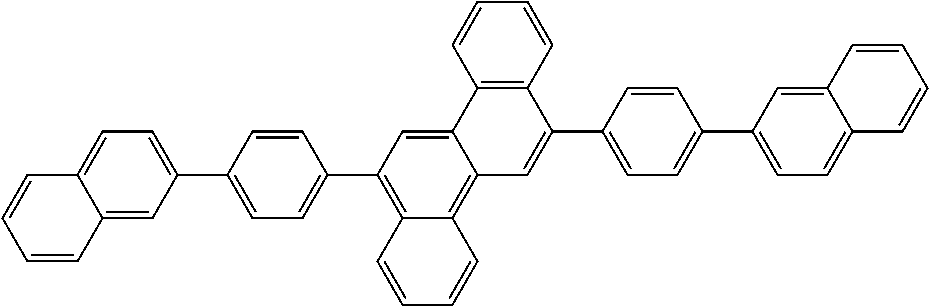 |
WO2011086863 |
| Green hosts |
| Arylcarbazoles |
 |
Appl. Phys. Lett. 78, 1622 (2001) |
 |
US20030175553 | |
 |
WO2001039234 | |
| Aryltriphenylene compounds |
 |
US20060280965 |
 |
US20060280965 | |
 |
WO2009021126 | |
| Poly-fused heteroaryl compounds |
 |
US20090309488 US20090302743 US20100012931 |
| Donor acceptor type molecules |
 |
WO2008056746 |
 |
WO2010107244 | |
| Aza-carbazole/DBT/DBF |
 |
JP2008074939 |
 |
US20100187984 | |
| Polymers (e.g., PVK) |
 |
Appl. Phys. Lett. 77, 2280 (2000) |
| Spirofluorene compounds |
 |
WO2004093207 |
| Metal phenoxybenzooxazole compounds |
 |
WO2005089025 |
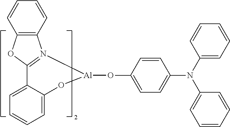 |
WO2006132173 | |
 |
JP200511610 | |
| Spirofluorene-carbazole compounds |
 |
JP2007254297 |
 |
JP2007254297 | |
| Indolocabazoles |
 |
WO2007063796 |
 |
WO2007063754 | |
| 5-member ring electron deficient heterocycles (e.g., triazole, oxadiazole) |
 |
J. Appl. Phys. 90, 5048 (2001) |
 |
WO2004107822 | |
| Tetraphenylene complexes |
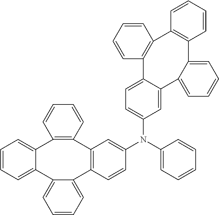 |
US20050112407 |
| Metal phenoxypyridine compounds |
 |
WO2005030900 |
| Metal coordination complexes (e.g., Zn, Al with N{circumflex over ( )}N ligands) |
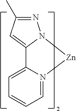 |
US20040137268, US20040137267 |
| Blue hosts |
| Arylcarbazoles |
 |
Appl. Phys. Lett, 82, 2422 (2003) |
 |
US20070190359 | |
| Dibenzothiophene/ Dibenzofuran- carbazole compounds |
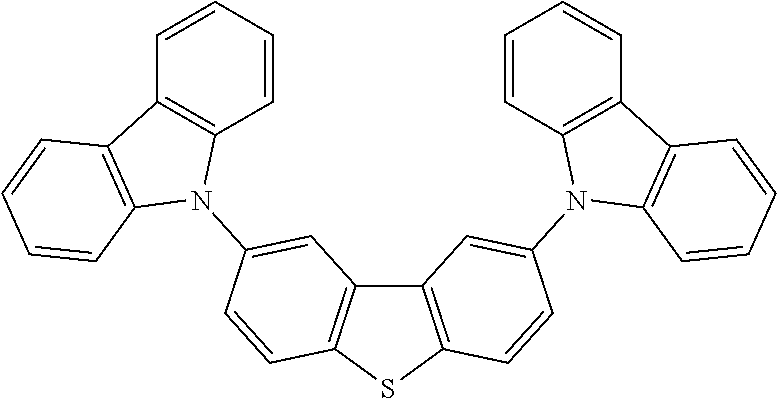 |
WO2006114966, US20090167162 |
 |
US20090167162 | |
 |
WO2009086028 | |
 |
US20090030202, US20090017330 | |
 |
US20100084966 | |
| Silicon aryl compounds |
 |
US20050238919 |
 |
WO2009003898 | |
| Silicon/Germanium aryl compounds |
 |
EP2034538A |
| Aryl benzoyl ester |
 |
WO2006100298 |
| Carbazole linked by non- conjugated groups |
 |
US20040115476 |
| Aza-carbazoles |
 |
US20060121308 |
| High triplet metal organometallic complex |
 |
U.S. Pat. No. 7,154,114 |
| Phosphorescent dopants |
| Red dopants |
| Heavy metal porphyrins (e.g., PtOEP) |
 |
Nature 395, 151 (1998) |
| Iridium(III) organometallic complexes |
 |
Appl. Phys. Lett. 78, 1622 (2001) |
 |
US2006835469 | |
 |
US2006835469 | |
 |
US20060202194 | |
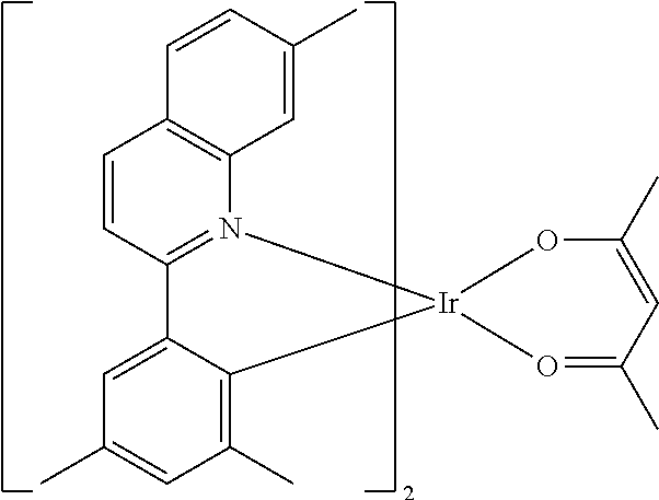 |
US20060202194 | |
 |
US20070087321 | |
 |
US20080261076 US20100090591 | |
 |
US20070087321 | |
 |
Adv. Mater. 19, 739 (2007) | |
 |
WO2009100991 | |
 |
WO2008101842 | |
 |
U.S. Pat. No. 7,232,618 | |
| Platinum(II) organometallic complexes |
 |
WO2003040257 |
 |
US20070103060 | |
| Osminum(III) complexes |
 |
Chem. Mater. 17, 3532 (2005) |
| Ruthenium(II) complexes |
 |
Adv. Mater. 17, 1059 (2005) |
| Rhenium (I), (II), and (III) complexes |
 |
US20050244673 |
| Green dopants |
| Iridium(III) organometallic complexes |
 |
Inorg. Chem. 40, 1704 (2001) |
 |
US20020034656 | |
 |
U.S. Pat. No. 7,332,232 | |
 |
US20090108737 | |
 |
WO2010028151 | |
 |
EP1841834B | |
 |
US20060127696 | |
 |
US20090039776 | |
 |
U.S. Pat. No. 6,921,915 | |
 |
US20100244004 | |
 |
U.S. Pat. No. 6,687,266 | |
 |
Chem. Mater. 16, 2480 (2004) | |
 |
US20070190359 | |
 |
US 20060008670 JP2007123392 | |
 |
WO2010086089, WO2011044988 | |
 |
Adv. Mater. 16, 2003 (2004) | |
 |
Angew. Chem. Int. Ed. 2006, 45, 7800 | |
 |
WO2009050290 | |
 |
US20090165846 | |
 |
US20080015355 | |
 |
US20010015432 | |
 |
US20100295032 | |
| Monomer for polymeric metal organometallic compounds |
 |
U.S. Pat. No. 7,250,226, U.S. Pat. No. 7,396,598 |
| Pt(II) organometallic complexes, including polydentated ligands |
 |
Appl. Phys. Lett. 86, 153505 (2005) |
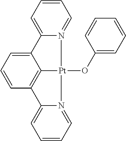 |
Appl. Phys. Lett. 86, 153505 (2005) | |
 |
Chem. Lett. 34, 592 (2005) | |
 |
WO2002015645 | |
 |
US20060263635 | |
 |
US20060182992 US20070103060 | |
| Cu complexes |
 |
WO2009000673 |
 |
US20070111026 | |
| Gold complexes |
 |
Chem. Commun. 2906 (2005) |
| Rhenium(III) complexes |
 |
Inorg. Chem. 42, 1248 (2003) |
| Osmium(II) complexes |
 |
U.S. Pat. No. 7,279,704 |
| Deuterated organometallic complexes |
 |
US20030138657 |
| Organometallic complexes with two or more metal centers |
 |
US20030152802 |
 |
U.S. Pat. No. 7,090,928 | |
| Blue dopants |
| Iridium(III) organometallic complexes |
 |
WO2002002714 |
 |
WO2006009024 | |
 |
US20060251923 US20110057559 US20110204333 | |
 |
U.S. Pat. No. 7,393,599, WO2006056418, US20050260441, WO2005019373 | |
 |
U.S. Pat. No. 7,534,505 | |
 |
WO2011051404 | |
 |
U.S. Pat. No. 7,445,855 | |
 |
US20070190359, US20080297033 US20100148663 | |
 |
U.S. Pat. No. 7,338,722 | |
 |
US20020134984 | |
 |
Angew. Chem. Int. Ed. 47, 1 (2008) | |
 |
Chem. Mater. 18, 5119 (2006) | |
 |
Inorg. Chem. 46, 4308 (2007) | |
 |
WO2005123873 | |
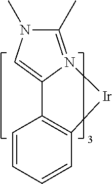 |
WO2005123873 | |
 |
WO2007004380 | |
 |
WO2006082742 | |
| Osmium(II) complexes |
 |
U.S. Pat. No. 7,279,704 |
 |
Organometallics 23, 3745 (2004) | |
| Gold complexes |
|
Appl. Phys. Lett.74, 1361 (1999) |
| Platinum(II) complexes |
 |
WO2006098120, WO2006103874 |
| Pt tetradentate complexes with at least one metal- carbene bond |
 |
U.S. Pat. No. 7,655,323 |
| Exciton/hole blocking layer materials |
| Bathocuprine compounds (e.g., BCP, BPhen) |
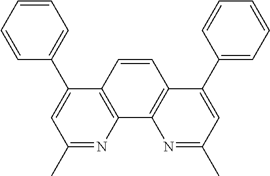 |
Appl. Phys. Lett. 75, 4 (1999) |
 |
Appl. Phys. Lett. 79, 449 (2001) | |
| Metal 8-hydroxyquinolates (e.g., BAlq) |
 |
Appl. Phys. Lett. 81, 162 (2002) |
| 5-member ring electron deficient heterocycles such as triazole, oxadiazole, imidazole, benzoimidazole |
 |
Appl. Phys. Lett. 81, 162 (2002) |
| Triphenylene compounds |
 |
US20050025993 |
| Fluorinated aromatic compounds |
 |
Appl. Phys. Lett. 79, 156 (2001) |
| Phenothiazine-S-oxide |
 |
WO2008132085 |
| Silylated five-membered nitrogen, oxygen, sulfur or phosphorus dibenzoheterocycles |
 |
WO2010079051 |
| Aza-carbazoles |
 |
US20060121308 |
| Electron transporting materials |
| Anthracene-benzoimidazole compounds |
 |
WO2003060956 |
 |
US20090179554 | |
| Aza triphenylene derivatives |
 |
US20090115316 |
| Anthracene-benzothiazole compounds |
 |
Appl. Phys. Lett. 89, 063504 (2006) |
| Metal 8-hydroxyquinolates (e.g., Alq3, Zrq4) |
 |
Appl. Phys. Lett. 51, 913 (1987) U.S. Pat. No. 7,230,107 |
| Metal hydroxybenoquinolates |
 |
Chem. Lett. 5, 905 (1993) |
| Bathocuprine compounds such as BCP, BPhen, etc |
 |
Appl. Phys. Lett. 91, 263503 (2007) |
 |
Appl. Phys. Lett. 79, 449 (2001) | |
| 5-member ring electron deficient heterocycles (e.g.,triazole, oxadiazole, imidazole, benzoimidazole) |
 |
Appl. Phys. Lett. 74, 865 (1999) |
 |
Appl. Phys. Lett. 55, 1489 (1989) | |
 |
Jpn. J. Apply. Phys. 32, L917 (1993) | |
| Silole compounds |
 |
Org. Electron. 4, 113 (2003) |
| Arylborane compounds |
 |
J. Am. Chem. Soc. 120, 9714 (1998) |
| Fluorinated aromatic compounds |
 |
J. Am. Chem. Soc. 122, 1832 (2000) |
| Fullerene (e.g., C60) |
 |
US20090101870 |
| Triazine complexes |
 |
US20040036077 |
| Zn (N{circumflex over ( )}N) complexes |
 |
U.S. Pat. No. 6,528,187 |


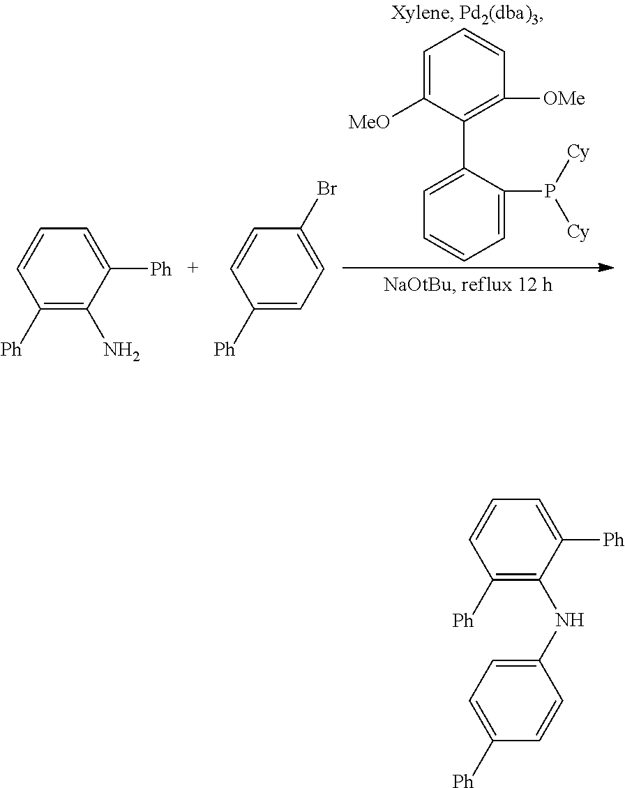


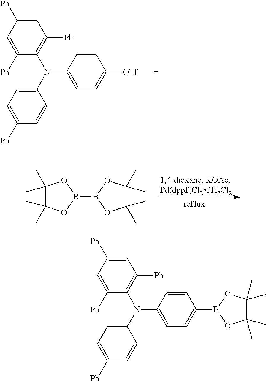


| TABLE 3A |
| Device structure and data |
| Device | 1931 CIE |
| Example | HTL 250Å | EML 300Å | BL 50Å | x | y |
| 1-1 | Cmpd 4 | Cmpd A: | Cmpd A | 0.176 | 0.390 |
| Cmpd C 15% | |||||
| 1-2 | Cmpd 5 | Cmpd A: | Cmpd A | 0.177 | 0.405 |
| Cmpd C 15% | |||||
| 1-3 | Cmpd 9 | Cmpd A: | Cmpd A | 0.178 | 0.405 |
| Cmpd C 15% | |||||
| 1-4 | |
Cmpd A: | Cmpd A | 0.176 | 0.401 |
| Cmpd C 15% | |||||
| Comparative | Comparative | Cmpd A: | Cmpd A | 0.175 | 0.390 |
| 1-1 | |
Cmpd C 15% | |||
| Comparative | NPD | Cmpd A: | Cmpd A | 0.176 | 0.395 |
| 1-2 | Cmpd C 15% | ||||
| 2-1 | Cmpd 2 | Cmpd A: | Cmpd A | 0.182 | 0.409 |
| Cmpd C 18% | |||||
| Comparative | NPD | Cmpd A: | Cmpd A | 0.182 | 0.409 |
| 2 | Cmpd C 18% | ||||
| 3-1 | Cmpd 8 | Cmpd B: | Cmpd A | 0.181 | 0.409 |
| Cmpd C 18% | |||||
| Comparative | NPD | Cmpd B: | Cmpd A | 0.181 | 0.409 |
| 3 | Cmpd C 18% | ||||
| 4-1 | Cmpd 3 | Cmpd B: | Cmpd B | 0.182 | 0.413 |
| Cmpd C 20% | |||||
| Comparative | NPD | Cmpd B: | Cmpd B | 0.181 | 0.410 |
| 4 | Cmpd C 20% | ||||
| TABLE 3B |
| Device structure and data |
| At 1000 cd/m2 | J = 40 mA/cm2 |
| Device | Voltage | LE | EQE | PE | L0 | LT80% |
| Example | [V] | [cd/A] | [%] | [lm/W] | [cd/m2] | [h] |
| 1-1 | 6.2 | 48.1 | 21.4 | 24.6 | 7641 | 33 |
| 1-2 | 6 | 50.9 | 21.9 | 26.5 | 8047 | 55 |
| 1-3 | 6.1 | 50.2 | 21.6 | 25.9 | 7847 | 54 |
| 1-4 | 6.1 | 49.8 | 21.6 | 25.7 | 7790 | 32 |
| Comparative 1-1 | 5.9 | 50.5 | 22.4 | 26.7 | 7903 | 24 |
| Comparative 1-2 | 6 | 46.7 | 20.5 | 24.4 | 7295 | 36 |
| 2-1 | 6 | 41.8 | 17.9 | 22 | 7202 | 67 |
| Comparative 2 | 6.1 | 40.7 | 17.5 | 20.9 | 6920 | 52 |
| 3-1 | 7.2 | 48.5 | 20.8 | 21.3 | 7605 | 91 |
| Comparative 3 | 7.3 | 46.6 | 20 | 20.1 | 7230 | 90 |
| 4-1 | 6.6 | 45.6 | 19.4 | 21.7 | 7360 | 76 |
| Comparative 4 | 6.6 | 44.1 | 18.8 | 20.9 | 7047 | 78 |
| TABLE 4A |
| Device structure and data |
| Device | 1931 CIE |
| Example | HTL 550Å | EML 300Å | BL 50Å | x | y |
| 5-1 | Cmpd 4 | Cmpd D: | Cmpd D | 0.319 | 0.630 |
| Cmpd E 12% | |||||
| Comparative | Comparative | Cmpd D: | Cmpd D | 0.333 | 0.623 |
| 5-1 | |
Cmpd E 12% | |||
| Comparative | NPD | Cmpd D: | Cmpd D | 0.337 | 0.621 |
| 5-2 | Cmpd E 12% | ||||
| TABLE 4B |
| Device structure and data |
| At 1000 cd/m2 | J = 40 mA/cm2 |
| Device | Voltage | LE | EQE | PE | L0 | LT80% |
| Example | [V] | [cd/A] | [%] | [lm/W] | [cd/m2] | [h] |
| 5-1 | 4.9 | 65.8 | 18.1 | 42.3 | 20528 | 420 |
| Comparative 5-1 | 4.8 | 72.5 | 19.7 | 47.7 | 23230 | 304 |
| Comparative 5-2 | 4.9 | 66.5 | 18.1 | 42.9 | 20320 | 358 |
Claims (11)


Priority Applications (5)
| Application Number | Priority Date | Filing Date | Title |
|---|---|---|---|
| US13/705,468 US8716484B1 (en) | 2012-12-05 | 2012-12-05 | Hole transporting materials with twisted aryl groups |
| KR1020130145140A KR102166509B1 (en) | 2012-12-05 | 2013-11-27 | Hole transporting materials with twisted aryl groups |
| DE102013020303.1A DE102013020303A1 (en) | 2012-12-05 | 2013-12-03 | Hole transport materials with twisted aryl groups |
| KR1020200126860A KR102373739B1 (en) | 2012-12-05 | 2020-09-29 | Hole transporting materials with twisted aryl groups |
| KR1020220028329A KR102430691B1 (en) | 2012-12-05 | 2022-03-04 | Hole transporting materials with twisted aryl groups |
Applications Claiming Priority (1)
| Application Number | Priority Date | Filing Date | Title |
|---|---|---|---|
| US13/705,468 US8716484B1 (en) | 2012-12-05 | 2012-12-05 | Hole transporting materials with twisted aryl groups |
Publications (1)
| Publication Number | Publication Date |
|---|---|
| US8716484B1 true US8716484B1 (en) | 2014-05-06 |
Family
ID=50552779
Family Applications (1)
| Application Number | Title | Priority Date | Filing Date |
|---|---|---|---|
| US13/705,468 Active US8716484B1 (en) | 2012-12-05 | 2012-12-05 | Hole transporting materials with twisted aryl groups |
Country Status (3)
| Country | Link |
|---|---|
| US (1) | US8716484B1 (en) |
| KR (3) | KR102166509B1 (en) |
| DE (1) | DE102013020303A1 (en) |
Cited By (3)
| Publication number | Priority date | Publication date | Assignee | Title |
|---|---|---|---|---|
| US20160133847A1 (en) * | 2013-06-19 | 2016-05-12 | Idemitsu Kosan Co., Ltd. | Aromatic amine derivative and organic electroluminescent element |
| CN108569970A (en) * | 2017-10-19 | 2018-09-25 | 北京鼎材科技有限公司 | The triarylamine compounds of benzidine type and organic electroluminescence device comprising it |
| US11322705B2 (en) | 2015-04-17 | 2022-05-03 | Samsung Display Co., Ltd. | Organic light-emitting device |
Citations (153)
| Publication number | Priority date | Publication date | Assignee | Title |
|---|---|---|---|---|
| US4769292A (en) | 1987-03-02 | 1988-09-06 | Eastman Kodak Company | Electroluminescent device with modified thin film luminescent zone |
| US5061569A (en) | 1990-07-26 | 1991-10-29 | Eastman Kodak Company | Electroluminescent device with organic electroluminescent medium |
| US5247190A (en) | 1989-04-20 | 1993-09-21 | Cambridge Research And Innovation Limited | Electroluminescent devices |
| US5550290A (en) * | 1993-10-13 | 1996-08-27 | Mita Industrial Co. Ltd. | Benzidine derivative and electrophotosensitive material using the same |
| US5703436A (en) | 1994-12-13 | 1997-12-30 | The Trustees Of Princeton University | Transparent contacts for organic devices |
| US5707745A (en) | 1994-12-13 | 1998-01-13 | The Trustees Of Princeton University | Multicolor organic light emitting devices |
| US5834893A (en) | 1996-12-23 | 1998-11-10 | The Trustees Of Princeton University | High efficiency organic light emitting devices with light directing structures |
| US5844363A (en) | 1997-01-23 | 1998-12-01 | The Trustees Of Princeton Univ. | Vacuum deposited, non-polymeric flexible organic light emitting devices |
| US6013982A (en) | 1996-12-23 | 2000-01-11 | The Trustees Of Princeton University | Multicolor display devices |
| US6087196A (en) | 1998-01-30 | 2000-07-11 | The Trustees Of Princeton University | Fabrication of organic semiconductor devices using ink jet printing |
| US6091195A (en) | 1997-02-03 | 2000-07-18 | The Trustees Of Princeton University | Displays having mesa pixel configuration |
| US6097147A (en) | 1998-09-14 | 2000-08-01 | The Trustees Of Princeton University | Structure for high efficiency electroluminescent device |
| US20010015432A1 (en) | 2000-02-10 | 2001-08-23 | Tatsuya Igarashi | Light emitting device material comprising iridium complex and light emitting device using same material |
| US6294398B1 (en) | 1999-11-23 | 2001-09-25 | The Trustees Of Princeton University | Method for patterning devices |
| US6303238B1 (en) | 1997-12-01 | 2001-10-16 | The Trustees Of Princeton University | OLEDs doped with phosphorescent compounds |
| JP2001316338A (en) | 2000-02-28 | 2001-11-13 | Yasuhiko Shirota | Electroluminescent element |
| US6337102B1 (en) | 1997-11-17 | 2002-01-08 | The Trustees Of Princeton University | Low pressure vapor phase deposition of organic thin films |
| US20020034656A1 (en) | 1998-09-14 | 2002-03-21 | Thompson Mark E. | Organometallic complexes as phosphorescent emitters in organic LEDs |
| US20020134984A1 (en) | 2001-02-01 | 2002-09-26 | Fuji Photo Film Co., Ltd. | Transition metal complex and light-emitting device |
| US20020158242A1 (en) | 1999-12-31 | 2002-10-31 | Se-Hwan Son | Electronic device comprising organic compound having p-type semiconducting characteristics |
| US6528187B1 (en) | 1998-09-08 | 2003-03-04 | Fuji Photo Film Co., Ltd. | Material for luminescence element and luminescence element using the same |
| US20030138657A1 (en) | 2000-12-07 | 2003-07-24 | Canon Kabushiki Kaisha | Deuterated semi-conducting organic compounds used for opto-electronic devices |
| US20030152802A1 (en) | 2001-06-19 | 2003-08-14 | Akira Tsuboyama | Metal coordination compound and organic liminescence device |
| US20030162053A1 (en) | 1996-06-25 | 2003-08-28 | Marks Tobin J. | Organic light - emitting diodes and methods for assembly and enhanced charge injection |
| US20030175553A1 (en) | 2001-12-28 | 2003-09-18 | Thompson Mark E. | White light emitting oleds from combined monomer and aggregate emission |
| US20030230980A1 (en) | 2002-06-18 | 2003-12-18 | Forrest Stephen R | Very low voltage, high efficiency phosphorescent oled in a p-i-n structure |
| US6687266B1 (en) | 2002-11-08 | 2004-02-03 | Universal Display Corporation | Organic light emitting materials and devices |
| US20040036077A1 (en) | 2002-08-22 | 2004-02-26 | Fuji Photo Film Co., Ltd. | Light emitting element |
| US20040115476A1 (en) | 2002-11-26 | 2004-06-17 | Tomohiro Oshiyama | Organic electroluminescent element, and display and illuminator |
| US20040137267A1 (en) | 2002-12-27 | 2004-07-15 | Fuji Photo Film Co., Ltd. | Organic electroluminescent device |
| US20040137268A1 (en) | 2002-12-27 | 2004-07-15 | Fuji Photo Film Co., Ltd. | Organic electroluminescent device |
| US20040174116A1 (en) | 2001-08-20 | 2004-09-09 | Lu Min-Hao Michael | Transparent electrodes |
| WO2004107822A1 (en) | 2003-05-29 | 2004-12-09 | Nippon Steel Chemical Co., Ltd. | Organic electroluminescent element |
| US20050025993A1 (en) | 2003-07-25 | 2005-02-03 | Thompson Mark E. | Materials and structures for enhancing the performance of organic light emitting devices |
| WO2005014551A1 (en) | 2003-08-07 | 2005-02-17 | Nippon Steel Chemical Co., Ltd. | Aluminum chelate compelx for organic el material |
| WO2005019373A2 (en) | 2003-08-19 | 2005-03-03 | Basf Aktiengesellschaft | Transition metal complexes comprising carbene ligands serving as emitters for organic light-emitting diodes (oled's) |
| WO2005030900A1 (en) | 2003-09-25 | 2005-04-07 | Nippon Steel Chemical Co., Ltd. | Organic electroluminescent device |
| US20050112407A1 (en) | 2003-11-21 | 2005-05-26 | Fuji Photo Film Co., Ltd. | Organic electroluminescent device |
| WO2004093207A3 (en) | 2003-04-15 | 2005-06-09 | Covion Organic Semiconductors | Mixtures of matrix materials and organic semiconductors capable of emission, use of the same and electronic components containing said mixtures |
| US20050123751A1 (en) | 2003-08-25 | 2005-06-09 | Tetsuo Tsutsui | Electrode device for organic device, electronic device having electrode device for organic device, and method of forming electrode device for organic device |
| US6921915B2 (en) | 2001-03-08 | 2005-07-26 | Canon Kabushiki Kaisha | Metal coordination compound, luminescence device and display apparatus |
| WO2005089025A1 (en) | 2004-03-15 | 2005-09-22 | Nippon Steel Chemical Co., Ltd. | Organic electroluminescent device |
| US20050238919A1 (en) | 2004-04-23 | 2005-10-27 | Fuji Photo Film Co., Ltd. | Organic electroluminescent device |
| US20050244673A1 (en) | 2002-08-27 | 2005-11-03 | Fujitsu Limited | Organometallic complex, organic EL element and organic EL display |
| US20050260441A1 (en) | 2004-05-18 | 2005-11-24 | Thompson Mark E | Luminescent compounds with carbene ligands |
| WO2005123873A1 (en) | 2004-06-17 | 2005-12-29 | Konica Minolta Holdings, Inc. | Organic electroluminescent device material, organic electroluminescent device, display and illuminating device |
| US20060008670A1 (en) | 2004-07-06 | 2006-01-12 | Chun Lin | Organic light emitting materials and devices |
| WO2006009024A1 (en) | 2004-07-23 | 2006-01-26 | Konica Minolta Holdings, Inc. | Organic electroluminescent device, display and illuminating device |
| US20060121308A1 (en) | 2003-04-23 | 2006-06-08 | Eisaku Katoh | Material for organic electroluminescent device, organic electroluminescent device, illuminating device and display |
| US20060127696A1 (en) | 2002-08-24 | 2006-06-15 | Covion Organic Semiconductors Gmbh | Rhodium and iridium complexes |
| WO2006082742A1 (en) | 2005-02-04 | 2006-08-10 | Konica Minolta Holdings, Inc. | Organic electroluminescent device material, organic electroluminescent device, display and illuminating device |
| US7090928B2 (en) | 2003-04-01 | 2006-08-15 | The University Of Southern California | Binuclear compounds |
| US20060182992A1 (en) | 2003-06-02 | 2006-08-17 | Kazumi Nii | Organic electroluminescent devices and metal complex compounds |
| US20060202194A1 (en) | 2005-03-08 | 2006-09-14 | Jeong Hyun C | Red phosphorescene compounds and organic electroluminescence device using the same |
| WO2006098120A1 (en) | 2005-03-16 | 2006-09-21 | Konica Minolta Holdings, Inc. | Organic electroluminescent device material and organic electroluminescent device |
| WO2006100298A1 (en) | 2005-03-24 | 2006-09-28 | Basf Aktiengesellschaft | Use of compounds containing aromatic or heteroaromatic rings linked via carbonyl group-containing groups, for use as matrix materials in organic light-emitting diodes |
| WO2006103874A1 (en) | 2005-03-29 | 2006-10-05 | Konica Minolta Holdings, Inc. | Organic electroluminescent device material, organic electroluminescent device, display and illuminating device |
| US20060240279A1 (en) | 2005-04-21 | 2006-10-26 | Vadim Adamovich | Non-blocked phosphorescent OLEDs |
| WO2006114966A1 (en) | 2005-04-18 | 2006-11-02 | Konica Minolta Holdings, Inc. | Organic electroluminescent device, display and illuminating device |
| US20060251923A1 (en) | 2005-05-06 | 2006-11-09 | Chun Lin | Stability OLED materials and devices |
| US20060263635A1 (en) | 2005-05-06 | 2006-11-23 | Fuji Photo Film Co., Ltd. | Organic electroluminescent device |
| US20060280965A1 (en) | 2005-05-31 | 2006-12-14 | Raymond Kwong | Triphenylene hosts in phosphorescent light emitting diodes |
| WO2006132173A1 (en) | 2005-06-07 | 2006-12-14 | Nippon Steel Chemical Co., Ltd. | Organic metal complex and organic electroluminescent device using same |
| US7154114B2 (en) | 2004-05-18 | 2006-12-26 | Universal Display Corporation | Cyclometallated iridium carbene complexes for use as hosts |
| WO2007004380A1 (en) | 2005-07-01 | 2007-01-11 | Konica Minolta Holdings, Inc. | Organic electroluminescent element material, organic electroluminescent element, display device, and lighting equipment |
| WO2006056418A8 (en) | 2004-11-25 | 2007-03-01 | Basf Ag | Use of transition metal carbene complexes in organic light-emitting diodes (oleds) |
| WO2006072002A3 (en) | 2004-12-30 | 2007-03-01 | Du Pont | Organometallic complexes |
| US20070087321A1 (en) | 2003-09-09 | 2007-04-19 | Csaba Pribenszky | Post-thaw survival of chryopreserved biological material by hydrostatic pressure challenge |
| US20070103060A1 (en) | 2003-11-04 | 2007-05-10 | Takasago International Corporation | Platinum complex and light emitting device |
| JP2007123392A (en) | 2005-10-26 | 2007-05-17 | Konica Minolta Holdings Inc | Organic electroluminescence device, display device and lighting device |
| US20070111026A1 (en) | 2005-11-15 | 2007-05-17 | Deaton Joseph C | Oled devices with dinuclear copper compounds |
| WO2007063754A1 (en) | 2005-12-01 | 2007-06-07 | Nippon Steel Chemical Co., Ltd. | Compound for organic electroluminescent element and organic electroluminescent element |
| WO2007063796A1 (en) | 2005-12-01 | 2007-06-07 | Nippon Steel Chemical Co., Ltd. | Organic electroluminescent device |
| US7230107B1 (en) | 2004-12-29 | 2007-06-12 | E. I. Du Pont De Nemours And Company | Metal quinoline complexes |
| US7232618B2 (en) | 2002-04-12 | 2007-06-19 | Canon Kabushiki Kaisha | Organic light-emitting device |
| US7250226B2 (en) | 2001-08-31 | 2007-07-31 | Nippon Hoso Kyokai | Phosphorescent compound, a phosphorescent composition and an organic light-emitting device |
| US20070190359A1 (en) | 2006-02-10 | 2007-08-16 | Knowles David B | Metal complexes of cyclometallated imidazo[1,2-ƒ]phenanthridine and diimidazo[1,2-a:1',2'-c]quinazoline ligands and isoelectronic and benzannulated analogs thereof |
| WO2007002683A3 (en) | 2005-06-27 | 2007-09-20 | Du Pont | Electrically conductive polymer compositions |
| JP2007254297A (en) | 2006-03-20 | 2007-10-04 | Nippon Steel Chem Co Ltd | Compound of light-emitting layer and organic electroluminescent device |
| US7279704B2 (en) | 2004-05-18 | 2007-10-09 | The University Of Southern California | Complexes with tridentate ligands |
| US20070278938A1 (en) | 2006-04-26 | 2007-12-06 | Idemitsu Kosan Co., Ltd. | Aromatic amine derivative and electroluminescence device using the same |
| US20080015355A1 (en) | 2004-06-28 | 2008-01-17 | Thomas Schafer | Electroluminescent Metal Complexes With Triazoles And Benzotriazoles |
| US7332232B2 (en) | 2004-02-03 | 2008-02-19 | Universal Display Corporation | OLEDs utilizing multidentate ligand systems |
| US7338722B2 (en) | 2003-03-24 | 2008-03-04 | The University Of Southern California | Phenyl and fluorenyl substituted phenyl-pyrazole complexes of Ir |
| JP2008074939A (en) | 2006-09-21 | 2008-04-03 | Konica Minolta Holdings Inc | Organic electroluminescence element material, organic electroluminescence element, display device and illumination device |
| US20080106190A1 (en) | 2006-08-23 | 2008-05-08 | Idemitsu Kosan Co., Ltd. | Aromatic amine derivatives and organic electroluminescent device using same |
| WO2008057394A1 (en) | 2006-11-01 | 2008-05-15 | The Trustees Of Princeton University | Hybrid layers for use in coatings on electronic devices or other articles |
| WO2008056746A1 (en) | 2006-11-09 | 2008-05-15 | Nippon Steel Chemical Co., Ltd. | Compound for organic electroluminescent device and organic electroluminescent device |
| US20080124572A1 (en) | 2006-11-24 | 2008-05-29 | Idemitsu Kosan Co., Ltd. | Aromatic amine derivative and organic electroluminescence device using the same |
| US7393599B2 (en) | 2004-05-18 | 2008-07-01 | The University Of Southern California | Luminescent compounds with carbene ligands |
| US7396598B2 (en) | 2001-06-20 | 2008-07-08 | Showa Denko K.K. | Light emitting material and organic light-emitting device |
| JP2008159779A (en) | 2006-12-22 | 2008-07-10 | Sony Corp | Organic electroluminescence element and display |
| WO2008101842A1 (en) | 2007-02-23 | 2008-08-28 | Basf Se | Electroluminescent metal complexes with benzotriazoles |
| US20080220265A1 (en) | 2006-12-08 | 2008-09-11 | Universal Display Corporation | Cross-linkable Iridium Complexes and Organic Light-Emitting Devices Using the Same |
| US7431968B1 (en) | 2001-09-04 | 2008-10-07 | The Trustees Of Princeton University | Process and apparatus for organic vapor jet deposition |
| US20080261076A1 (en) | 2007-03-08 | 2008-10-23 | Universal Display Corporation | Phosphorescent materials |
| US7445855B2 (en) | 2004-05-18 | 2008-11-04 | The University Of Southern California | Cationic metal-carbene complexes |
| WO2008132085A1 (en) | 2007-04-26 | 2008-11-06 | Basf Se | Silanes containing phenothiazine-s-oxide or phenothiazine-s,s-dioxide groups and the use thereof in oleds |
| US20080297033A1 (en) | 2006-02-10 | 2008-12-04 | Knowles David B | Blue phosphorescent imidazophenanthridine materials |
| WO2009000673A2 (en) | 2007-06-22 | 2008-12-31 | Basf Se | Light emitting cu(i) complexes |
| US20090009065A1 (en) | 2007-07-07 | 2009-01-08 | Idemitsu Kosan Co., Ltd. | Organic electroluminescence device and material for organic electroluminescence device |
| US20090008605A1 (en) | 2007-07-07 | 2009-01-08 | Idemitsu Kosan Co., Ltd. | Naphthalene derivative, material for organic electroluminescence device, and organic electroluminescence device using the same |
| WO2009003898A1 (en) | 2007-07-05 | 2009-01-08 | Basf Se | Organic light-emitting diodes containing carbene transition metal complex emitters and at least one compound selected from disilylcarbazoles, disilyldibenzofurans, disilyldibenzothiophenes, disilyldibenzophospholes, disilyldibenzothiophene s-oxides and disilyldibenzothiophene s,s-dioxides |
| WO2009008311A1 (en) | 2007-07-07 | 2009-01-15 | Idemitsu Kosan Co., Ltd. | Chrysene derivative and organic electroluminescent device using the same |
| US20090017330A1 (en) | 2007-07-10 | 2009-01-15 | Idemitsu Kosan Co., Ltd. | Material for organic electroluminescence device and organic electroluminescence device utilizing the same |
| US20090030202A1 (en) | 2007-07-10 | 2009-01-29 | Idemitsu Kosan Co., Ltd. | Material for organic electroluminescent element and organic electroluminescent element employing the same |
| WO2009018009A1 (en) | 2007-07-27 | 2009-02-05 | E. I. Du Pont De Nemours And Company | Aqueous dispersions of electrically conducting polymers containing inorganic nanoparticles |
| WO2009021126A2 (en) | 2007-08-08 | 2009-02-12 | Universal Display Corporation | Benzo-fused thiophene or benzo-fused furan compounds comprising a triphenylene group |
| US20090039776A1 (en) | 2007-08-09 | 2009-02-12 | Canon Kabushiki Kaisha | Organometallic complex and organic light-emitting element using same |
| US20090045731A1 (en) | 2007-07-07 | 2009-02-19 | Idemitsu Kosan Co., Ltd. | Organic electroluminescence device and material for organic electroluminescence device |
| US20090045730A1 (en) | 2007-07-07 | 2009-02-19 | Idemitsu Kosan Co., Ltd. | Organic electroluminescence device and material for organic electroluminescence device |
| WO2009050290A1 (en) | 2007-10-17 | 2009-04-23 | Basf Se | Transition metal complexes having bridged carbene ligands and the use thereof in oleds |
| US20090101870A1 (en) | 2007-10-22 | 2009-04-23 | E. I. Du Pont De Nemours And Company | Electron transport bi-layers and devices made with such bi-layers |
| US20090108737A1 (en) | 2006-12-08 | 2009-04-30 | Raymond Kwong | Light-emitting organometallic complexes |
| EP1841834B1 (en) | 2004-12-23 | 2009-05-06 | Ciba Holding Inc. | Electroluminescent metal complexes with nucleophilic carbene ligands |
| US20090115316A1 (en) | 2007-11-02 | 2009-05-07 | Shiying Zheng | Organic electroluminescent device having an azatriphenylene derivative |
| US7534505B2 (en) | 2004-05-18 | 2009-05-19 | The University Of Southern California | Organometallic compounds for use in electroluminescent devices |
| WO2009063833A1 (en) | 2007-11-15 | 2009-05-22 | Idemitsu Kosan Co., Ltd. | Benzochrysene derivative and organic electroluminescent device using the same |
| WO2009066779A1 (en) | 2007-11-22 | 2009-05-28 | Idemitsu Kosan Co., Ltd. | Organic el element |
| WO2009066778A1 (en) | 2007-11-22 | 2009-05-28 | Idemitsu Kosan Co., Ltd. | Organic el element and solution containing organic el material |
| US20090165846A1 (en) | 2005-09-07 | 2009-07-02 | Universitaet Braunschweig | Triplet emitter having condensed five-membered rings |
| US20090167162A1 (en) | 2007-12-28 | 2009-07-02 | Universal Display Corporation | Dibenzothiophene-containing materials in phosphorescent light emitting diodes |
| WO2009086028A2 (en) | 2007-12-28 | 2009-07-09 | Universal Display Corporation | Carbazole-containing materials in phosphorescent light emitting diodes |
| US20090179554A1 (en) | 2006-05-11 | 2009-07-16 | Hitoshi Kuma | Organic electroluminescent device |
| WO2009100991A1 (en) | 2008-02-12 | 2009-08-20 | Basf Se | Electroluminescent metal complexes with dibenzo[f,h]quinoxalines |
| US20090302743A1 (en) | 2008-06-05 | 2009-12-10 | Idemitsu Kosan Co., Ltd. | Material for organic electroluminescence device and organic electroluminescence device using the same |
| US20090309488A1 (en) | 2008-06-05 | 2009-12-17 | Idemitsu Kosan Co., Ltd. | Material for organic electroluminescence device and organic electroluminescence device using the same |
| US20100012931A1 (en) | 2008-06-05 | 2010-01-21 | Idemitsu Kosan Co., Ltd. | Polycyclic compounds and organic electroluminescence device employing the same |
| US7655323B2 (en) | 2004-05-18 | 2010-02-02 | The University Of Southern California | OLEDs utilizing macrocyclic ligand systems |
| WO2010028151A1 (en) | 2008-09-03 | 2010-03-11 | Universal Display Corporation | Phosphorescent materials |
| US20100084966A1 (en) | 2006-12-13 | 2010-04-08 | Konica Minolta Holdings, Inc. | Organic electroluminescent element, display device and lighting device |
| US20100090591A1 (en) | 2008-09-16 | 2010-04-15 | Universal Display Corporation | Phosphorescent materials |
| WO2010056066A1 (en) | 2008-11-13 | 2010-05-20 | Gracel Display Inc. | Novel organometallic compounds for electroluminescence and organic electroluminescent device using the same |
| US20100148663A1 (en) | 2008-12-12 | 2010-06-17 | Universal Display Corporation | Blue Emitter with High Efficiency Based on Imidazo[1,2-f] Phenanthridine Iridium Complexes |
| WO2010011390A3 (en) | 2008-05-07 | 2010-06-24 | The Trustees Of Princeton University | Hybrid layers for use in coatings on electronic devices or other articles |
| WO2010079051A1 (en) | 2009-01-07 | 2010-07-15 | Basf Se | Silyl and heteroatom substituted compounds selected from carbazoles, dibenzofurans, dibenzothiophenes and dibenzo phospholes and the application thereof in organic electronics |
| US20100187984A1 (en) | 2009-01-16 | 2010-07-29 | Universal Display Corporation | Materials with aza-dibenzothiophene or aza-dibenzofuran core for pholed |
| WO2010086089A1 (en) | 2009-02-02 | 2010-08-05 | Merck Patent Gmbh | Metal complexes |
| WO2010107244A2 (en) | 2009-03-20 | 2010-09-23 | Dow Advanced Display Materials, Ltd. | Novel organic electroluminescent compounds and organic electroluminescent device using the same |
| US20100244004A1 (en) | 2009-03-23 | 2010-09-30 | Universal Display Corporation | Heteroleptic iridium complex |
| US20100295032A1 (en) | 2009-05-20 | 2010-11-25 | Universal Display Corporation | Metal complexes with boron-nitrogen heterocycle containing ligands |
| US20110057559A1 (en) | 2007-12-28 | 2011-03-10 | Universal Display Corporation | Phosphorescent emitters and host materials with improved stability |
| WO2011044988A1 (en) | 2009-10-16 | 2011-04-21 | Merck Patent Gmbh | Metal complexes |
| WO2011051404A1 (en) | 2009-10-28 | 2011-05-05 | Basf Se | Heteroleptic carbene complexes and use thereof in organic electronics |
| WO2011075644A2 (en) | 2009-12-18 | 2011-06-23 | Plextronics, Inc. | Copolymers of 3,4-dialkoxythiophenes and methods for making and devices |
| US7968146B2 (en) | 2006-11-01 | 2011-06-28 | The Trustees Of Princeton University | Hybrid layers for use in coatings on electronic devices or other articles |
| US20110163302A1 (en) | 2008-06-30 | 2011-07-07 | Universal Display Corporation | Hole transport materials having a sulfur-containing group |
| WO2011086863A1 (en) | 2010-01-15 | 2011-07-21 | 富士フイルム株式会社 | Organic electroluminescent element |
| EP2350216A1 (en) | 2008-10-27 | 2011-08-03 | Plextronics, Inc. | Charge injection and transport layers |
| US20110204333A1 (en) | 2010-02-25 | 2011-08-25 | Universal Display Corporation | Phosphorescent emitters |
| JP2011173973A (en) | 2010-02-24 | 2011-09-08 | Toyo Ink Sc Holdings Co Ltd | Material for organic electroluminescent element and application thereof |
| EP1725079B1 (en) | 2004-03-11 | 2013-05-08 | Mitsubishi Chemical Corporation | Composition for charge-transporting film and ion compound, charge-transporting film and organic electroluminescent device using same, and method for manufacturing organic electroluminescent device and method for producing charge-transporting film |
| EP2034538B1 (en) | 2006-06-02 | 2013-10-09 | Idemitsu Kosan Co., Ltd. | Material for organic electroluminescence element, and organic electroluminescence element using the material |
Family Cites Families (2)
| Publication number | Priority date | Publication date | Assignee | Title |
|---|---|---|---|---|
| WO1995009147A1 (en) * | 1993-09-29 | 1995-04-06 | Idemitsu Kosan Co., Ltd. | Organic electroluminescent element and arylenediamine derivative |
| JP2012190863A (en) * | 2011-03-09 | 2012-10-04 | Toyo Ink Sc Holdings Co Ltd | Material for organic electroluminescent element and use thereof |
-
2012
- 2012-12-05 US US13/705,468 patent/US8716484B1/en active Active
-
2013
- 2013-11-27 KR KR1020130145140A patent/KR102166509B1/en active IP Right Grant
- 2013-12-03 DE DE102013020303.1A patent/DE102013020303A1/en active Pending
-
2020
- 2020-09-29 KR KR1020200126860A patent/KR102373739B1/en active IP Right Grant
-
2022
- 2022-03-04 KR KR1020220028329A patent/KR102430691B1/en active IP Right Grant
Patent Citations (155)
| Publication number | Priority date | Publication date | Assignee | Title |
|---|---|---|---|---|
| US4769292A (en) | 1987-03-02 | 1988-09-06 | Eastman Kodak Company | Electroluminescent device with modified thin film luminescent zone |
| US5247190A (en) | 1989-04-20 | 1993-09-21 | Cambridge Research And Innovation Limited | Electroluminescent devices |
| US5061569A (en) | 1990-07-26 | 1991-10-29 | Eastman Kodak Company | Electroluminescent device with organic electroluminescent medium |
| US5550290A (en) * | 1993-10-13 | 1996-08-27 | Mita Industrial Co. Ltd. | Benzidine derivative and electrophotosensitive material using the same |
| US5703436A (en) | 1994-12-13 | 1997-12-30 | The Trustees Of Princeton University | Transparent contacts for organic devices |
| US5707745A (en) | 1994-12-13 | 1998-01-13 | The Trustees Of Princeton University | Multicolor organic light emitting devices |
| US20030162053A1 (en) | 1996-06-25 | 2003-08-28 | Marks Tobin J. | Organic light - emitting diodes and methods for assembly and enhanced charge injection |
| US5834893A (en) | 1996-12-23 | 1998-11-10 | The Trustees Of Princeton University | High efficiency organic light emitting devices with light directing structures |
| US6013982A (en) | 1996-12-23 | 2000-01-11 | The Trustees Of Princeton University | Multicolor display devices |
| US5844363A (en) | 1997-01-23 | 1998-12-01 | The Trustees Of Princeton Univ. | Vacuum deposited, non-polymeric flexible organic light emitting devices |
| US6091195A (en) | 1997-02-03 | 2000-07-18 | The Trustees Of Princeton University | Displays having mesa pixel configuration |
| US6337102B1 (en) | 1997-11-17 | 2002-01-08 | The Trustees Of Princeton University | Low pressure vapor phase deposition of organic thin films |
| US6303238B1 (en) | 1997-12-01 | 2001-10-16 | The Trustees Of Princeton University | OLEDs doped with phosphorescent compounds |
| US6087196A (en) | 1998-01-30 | 2000-07-11 | The Trustees Of Princeton University | Fabrication of organic semiconductor devices using ink jet printing |
| US6528187B1 (en) | 1998-09-08 | 2003-03-04 | Fuji Photo Film Co., Ltd. | Material for luminescence element and luminescence element using the same |
| US6097147A (en) | 1998-09-14 | 2000-08-01 | The Trustees Of Princeton University | Structure for high efficiency electroluminescent device |
| US20020034656A1 (en) | 1998-09-14 | 2002-03-21 | Thompson Mark E. | Organometallic complexes as phosphorescent emitters in organic LEDs |
| US6294398B1 (en) | 1999-11-23 | 2001-09-25 | The Trustees Of Princeton University | Method for patterning devices |
| US6468819B1 (en) | 1999-11-23 | 2002-10-22 | The Trustees Of Princeton University | Method for patterning organic thin film devices using a die |
| US20020158242A1 (en) | 1999-12-31 | 2002-10-31 | Se-Hwan Son | Electronic device comprising organic compound having p-type semiconducting characteristics |
| US20010015432A1 (en) | 2000-02-10 | 2001-08-23 | Tatsuya Igarashi | Light emitting device material comprising iridium complex and light emitting device using same material |
| JP2001316338A (en) | 2000-02-28 | 2001-11-13 | Yasuhiko Shirota | Electroluminescent element |
| US20030138657A1 (en) | 2000-12-07 | 2003-07-24 | Canon Kabushiki Kaisha | Deuterated semi-conducting organic compounds used for opto-electronic devices |
| US20020134984A1 (en) | 2001-02-01 | 2002-09-26 | Fuji Photo Film Co., Ltd. | Transition metal complex and light-emitting device |
| US6921915B2 (en) | 2001-03-08 | 2005-07-26 | Canon Kabushiki Kaisha | Metal coordination compound, luminescence device and display apparatus |
| US20030152802A1 (en) | 2001-06-19 | 2003-08-14 | Akira Tsuboyama | Metal coordination compound and organic liminescence device |
| US7396598B2 (en) | 2001-06-20 | 2008-07-08 | Showa Denko K.K. | Light emitting material and organic light-emitting device |
| US20040174116A1 (en) | 2001-08-20 | 2004-09-09 | Lu Min-Hao Michael | Transparent electrodes |
| US7250226B2 (en) | 2001-08-31 | 2007-07-31 | Nippon Hoso Kyokai | Phosphorescent compound, a phosphorescent composition and an organic light-emitting device |
| US7431968B1 (en) | 2001-09-04 | 2008-10-07 | The Trustees Of Princeton University | Process and apparatus for organic vapor jet deposition |
| US20030175553A1 (en) | 2001-12-28 | 2003-09-18 | Thompson Mark E. | White light emitting oleds from combined monomer and aggregate emission |
| US7232618B2 (en) | 2002-04-12 | 2007-06-19 | Canon Kabushiki Kaisha | Organic light-emitting device |
| US20030230980A1 (en) | 2002-06-18 | 2003-12-18 | Forrest Stephen R | Very low voltage, high efficiency phosphorescent oled in a p-i-n structure |
| US20040036077A1 (en) | 2002-08-22 | 2004-02-26 | Fuji Photo Film Co., Ltd. | Light emitting element |
| US20060127696A1 (en) | 2002-08-24 | 2006-06-15 | Covion Organic Semiconductors Gmbh | Rhodium and iridium complexes |
| US20050244673A1 (en) | 2002-08-27 | 2005-11-03 | Fujitsu Limited | Organometallic complex, organic EL element and organic EL display |
| US6687266B1 (en) | 2002-11-08 | 2004-02-03 | Universal Display Corporation | Organic light emitting materials and devices |
| US20040115476A1 (en) | 2002-11-26 | 2004-06-17 | Tomohiro Oshiyama | Organic electroluminescent element, and display and illuminator |
| US20040137267A1 (en) | 2002-12-27 | 2004-07-15 | Fuji Photo Film Co., Ltd. | Organic electroluminescent device |
| US20040137268A1 (en) | 2002-12-27 | 2004-07-15 | Fuji Photo Film Co., Ltd. | Organic electroluminescent device |
| US7338722B2 (en) | 2003-03-24 | 2008-03-04 | The University Of Southern California | Phenyl and fluorenyl substituted phenyl-pyrazole complexes of Ir |
| US7090928B2 (en) | 2003-04-01 | 2006-08-15 | The University Of Southern California | Binuclear compounds |
| WO2004093207A3 (en) | 2003-04-15 | 2005-06-09 | Covion Organic Semiconductors | Mixtures of matrix materials and organic semiconductors capable of emission, use of the same and electronic components containing said mixtures |
| US20060121308A1 (en) | 2003-04-23 | 2006-06-08 | Eisaku Katoh | Material for organic electroluminescent device, organic electroluminescent device, illuminating device and display |
| WO2004107822A1 (en) | 2003-05-29 | 2004-12-09 | Nippon Steel Chemical Co., Ltd. | Organic electroluminescent element |
| US20060182992A1 (en) | 2003-06-02 | 2006-08-17 | Kazumi Nii | Organic electroluminescent devices and metal complex compounds |
| US20050025993A1 (en) | 2003-07-25 | 2005-02-03 | Thompson Mark E. | Materials and structures for enhancing the performance of organic light emitting devices |
| WO2005014551A1 (en) | 2003-08-07 | 2005-02-17 | Nippon Steel Chemical Co., Ltd. | Aluminum chelate compelx for organic el material |
| WO2005019373A2 (en) | 2003-08-19 | 2005-03-03 | Basf Aktiengesellschaft | Transition metal complexes comprising carbene ligands serving as emitters for organic light-emitting diodes (oled's) |
| US20050123751A1 (en) | 2003-08-25 | 2005-06-09 | Tetsuo Tsutsui | Electrode device for organic device, electronic device having electrode device for organic device, and method of forming electrode device for organic device |
| US20070087321A1 (en) | 2003-09-09 | 2007-04-19 | Csaba Pribenszky | Post-thaw survival of chryopreserved biological material by hydrostatic pressure challenge |
| WO2005030900A1 (en) | 2003-09-25 | 2005-04-07 | Nippon Steel Chemical Co., Ltd. | Organic electroluminescent device |
| US20070103060A1 (en) | 2003-11-04 | 2007-05-10 | Takasago International Corporation | Platinum complex and light emitting device |
| US20050112407A1 (en) | 2003-11-21 | 2005-05-26 | Fuji Photo Film Co., Ltd. | Organic electroluminescent device |
| US7332232B2 (en) | 2004-02-03 | 2008-02-19 | Universal Display Corporation | OLEDs utilizing multidentate ligand systems |
| EP1725079B1 (en) | 2004-03-11 | 2013-05-08 | Mitsubishi Chemical Corporation | Composition for charge-transporting film and ion compound, charge-transporting film and organic electroluminescent device using same, and method for manufacturing organic electroluminescent device and method for producing charge-transporting film |
| WO2005089025A1 (en) | 2004-03-15 | 2005-09-22 | Nippon Steel Chemical Co., Ltd. | Organic electroluminescent device |
| US20050238919A1 (en) | 2004-04-23 | 2005-10-27 | Fuji Photo Film Co., Ltd. | Organic electroluminescent device |
| US7393599B2 (en) | 2004-05-18 | 2008-07-01 | The University Of Southern California | Luminescent compounds with carbene ligands |
| US7445855B2 (en) | 2004-05-18 | 2008-11-04 | The University Of Southern California | Cationic metal-carbene complexes |
| US7655323B2 (en) | 2004-05-18 | 2010-02-02 | The University Of Southern California | OLEDs utilizing macrocyclic ligand systems |
| US7534505B2 (en) | 2004-05-18 | 2009-05-19 | The University Of Southern California | Organometallic compounds for use in electroluminescent devices |
| US7154114B2 (en) | 2004-05-18 | 2006-12-26 | Universal Display Corporation | Cyclometallated iridium carbene complexes for use as hosts |
| US7279704B2 (en) | 2004-05-18 | 2007-10-09 | The University Of Southern California | Complexes with tridentate ligands |
| US20050260441A1 (en) | 2004-05-18 | 2005-11-24 | Thompson Mark E | Luminescent compounds with carbene ligands |
| WO2005123873A1 (en) | 2004-06-17 | 2005-12-29 | Konica Minolta Holdings, Inc. | Organic electroluminescent device material, organic electroluminescent device, display and illuminating device |
| US20080015355A1 (en) | 2004-06-28 | 2008-01-17 | Thomas Schafer | Electroluminescent Metal Complexes With Triazoles And Benzotriazoles |
| US20060008670A1 (en) | 2004-07-06 | 2006-01-12 | Chun Lin | Organic light emitting materials and devices |
| WO2006009024A1 (en) | 2004-07-23 | 2006-01-26 | Konica Minolta Holdings, Inc. | Organic electroluminescent device, display and illuminating device |
| WO2006056418A8 (en) | 2004-11-25 | 2007-03-01 | Basf Ag | Use of transition metal carbene complexes in organic light-emitting diodes (oleds) |
| US20080018221A1 (en) | 2004-11-25 | 2008-01-24 | Basf Aktiengesellschaft | Use Of Transition Metal Carbene Complexes In Organic Light-Emitting Diodes (Oleds) |
| EP1841834B1 (en) | 2004-12-23 | 2009-05-06 | Ciba Holding Inc. | Electroluminescent metal complexes with nucleophilic carbene ligands |
| US7230107B1 (en) | 2004-12-29 | 2007-06-12 | E. I. Du Pont De Nemours And Company | Metal quinoline complexes |
| WO2006072002A3 (en) | 2004-12-30 | 2007-03-01 | Du Pont | Organometallic complexes |
| WO2006082742A1 (en) | 2005-02-04 | 2006-08-10 | Konica Minolta Holdings, Inc. | Organic electroluminescent device material, organic electroluminescent device, display and illuminating device |
| US20060202194A1 (en) | 2005-03-08 | 2006-09-14 | Jeong Hyun C | Red phosphorescene compounds and organic electroluminescence device using the same |
| WO2006098120A1 (en) | 2005-03-16 | 2006-09-21 | Konica Minolta Holdings, Inc. | Organic electroluminescent device material and organic electroluminescent device |
| WO2006100298A1 (en) | 2005-03-24 | 2006-09-28 | Basf Aktiengesellschaft | Use of compounds containing aromatic or heteroaromatic rings linked via carbonyl group-containing groups, for use as matrix materials in organic light-emitting diodes |
| WO2006103874A1 (en) | 2005-03-29 | 2006-10-05 | Konica Minolta Holdings, Inc. | Organic electroluminescent device material, organic electroluminescent device, display and illuminating device |
| WO2006114966A1 (en) | 2005-04-18 | 2006-11-02 | Konica Minolta Holdings, Inc. | Organic electroluminescent device, display and illuminating device |
| US20060240279A1 (en) | 2005-04-21 | 2006-10-26 | Vadim Adamovich | Non-blocked phosphorescent OLEDs |
| US20060263635A1 (en) | 2005-05-06 | 2006-11-23 | Fuji Photo Film Co., Ltd. | Organic electroluminescent device |
| US20060251923A1 (en) | 2005-05-06 | 2006-11-09 | Chun Lin | Stability OLED materials and devices |
| US20060280965A1 (en) | 2005-05-31 | 2006-12-14 | Raymond Kwong | Triphenylene hosts in phosphorescent light emitting diodes |
| WO2006132173A1 (en) | 2005-06-07 | 2006-12-14 | Nippon Steel Chemical Co., Ltd. | Organic metal complex and organic electroluminescent device using same |
| WO2007002683A3 (en) | 2005-06-27 | 2007-09-20 | Du Pont | Electrically conductive polymer compositions |
| WO2007004380A1 (en) | 2005-07-01 | 2007-01-11 | Konica Minolta Holdings, Inc. | Organic electroluminescent element material, organic electroluminescent element, display device, and lighting equipment |
| US20090165846A1 (en) | 2005-09-07 | 2009-07-02 | Universitaet Braunschweig | Triplet emitter having condensed five-membered rings |
| JP2007123392A (en) | 2005-10-26 | 2007-05-17 | Konica Minolta Holdings Inc | Organic electroluminescence device, display device and lighting device |
| US20070111026A1 (en) | 2005-11-15 | 2007-05-17 | Deaton Joseph C | Oled devices with dinuclear copper compounds |
| WO2007063796A1 (en) | 2005-12-01 | 2007-06-07 | Nippon Steel Chemical Co., Ltd. | Organic electroluminescent device |
| WO2007063754A1 (en) | 2005-12-01 | 2007-06-07 | Nippon Steel Chemical Co., Ltd. | Compound for organic electroluminescent element and organic electroluminescent element |
| US20080297033A1 (en) | 2006-02-10 | 2008-12-04 | Knowles David B | Blue phosphorescent imidazophenanthridine materials |
| US20070190359A1 (en) | 2006-02-10 | 2007-08-16 | Knowles David B | Metal complexes of cyclometallated imidazo[1,2-ƒ]phenanthridine and diimidazo[1,2-a:1',2'-c]quinazoline ligands and isoelectronic and benzannulated analogs thereof |
| JP2007254297A (en) | 2006-03-20 | 2007-10-04 | Nippon Steel Chem Co Ltd | Compound of light-emitting layer and organic electroluminescent device |
| US20070278938A1 (en) | 2006-04-26 | 2007-12-06 | Idemitsu Kosan Co., Ltd. | Aromatic amine derivative and electroluminescence device using the same |
| US20090179554A1 (en) | 2006-05-11 | 2009-07-16 | Hitoshi Kuma | Organic electroluminescent device |
| EP2034538B1 (en) | 2006-06-02 | 2013-10-09 | Idemitsu Kosan Co., Ltd. | Material for organic electroluminescence element, and organic electroluminescence element using the material |
| US20080106190A1 (en) | 2006-08-23 | 2008-05-08 | Idemitsu Kosan Co., Ltd. | Aromatic amine derivatives and organic electroluminescent device using same |
| JP2008074939A (en) | 2006-09-21 | 2008-04-03 | Konica Minolta Holdings Inc | Organic electroluminescence element material, organic electroluminescence element, display device and illumination device |
| WO2008057394A1 (en) | 2006-11-01 | 2008-05-15 | The Trustees Of Princeton University | Hybrid layers for use in coatings on electronic devices or other articles |
| US7968146B2 (en) | 2006-11-01 | 2011-06-28 | The Trustees Of Princeton University | Hybrid layers for use in coatings on electronic devices or other articles |
| WO2008056746A1 (en) | 2006-11-09 | 2008-05-15 | Nippon Steel Chemical Co., Ltd. | Compound for organic electroluminescent device and organic electroluminescent device |
| US20080124572A1 (en) | 2006-11-24 | 2008-05-29 | Idemitsu Kosan Co., Ltd. | Aromatic amine derivative and organic electroluminescence device using the same |
| US20090108737A1 (en) | 2006-12-08 | 2009-04-30 | Raymond Kwong | Light-emitting organometallic complexes |
| US20080220265A1 (en) | 2006-12-08 | 2008-09-11 | Universal Display Corporation | Cross-linkable Iridium Complexes and Organic Light-Emitting Devices Using the Same |
| US20100084966A1 (en) | 2006-12-13 | 2010-04-08 | Konica Minolta Holdings, Inc. | Organic electroluminescent element, display device and lighting device |
| JP2008159779A (en) | 2006-12-22 | 2008-07-10 | Sony Corp | Organic electroluminescence element and display |
| WO2008101842A1 (en) | 2007-02-23 | 2008-08-28 | Basf Se | Electroluminescent metal complexes with benzotriazoles |
| US20080261076A1 (en) | 2007-03-08 | 2008-10-23 | Universal Display Corporation | Phosphorescent materials |
| WO2008132085A1 (en) | 2007-04-26 | 2008-11-06 | Basf Se | Silanes containing phenothiazine-s-oxide or phenothiazine-s,s-dioxide groups and the use thereof in oleds |
| WO2009000673A2 (en) | 2007-06-22 | 2008-12-31 | Basf Se | Light emitting cu(i) complexes |
| WO2009003898A1 (en) | 2007-07-05 | 2009-01-08 | Basf Se | Organic light-emitting diodes containing carbene transition metal complex emitters and at least one compound selected from disilylcarbazoles, disilyldibenzofurans, disilyldibenzothiophenes, disilyldibenzophospholes, disilyldibenzothiophene s-oxides and disilyldibenzothiophene s,s-dioxides |
| US20090009065A1 (en) | 2007-07-07 | 2009-01-08 | Idemitsu Kosan Co., Ltd. | Organic electroluminescence device and material for organic electroluminescence device |
| US20090045731A1 (en) | 2007-07-07 | 2009-02-19 | Idemitsu Kosan Co., Ltd. | Organic electroluminescence device and material for organic electroluminescence device |
| US20090008605A1 (en) | 2007-07-07 | 2009-01-08 | Idemitsu Kosan Co., Ltd. | Naphthalene derivative, material for organic electroluminescence device, and organic electroluminescence device using the same |
| US20090045730A1 (en) | 2007-07-07 | 2009-02-19 | Idemitsu Kosan Co., Ltd. | Organic electroluminescence device and material for organic electroluminescence device |
| WO2009008311A1 (en) | 2007-07-07 | 2009-01-15 | Idemitsu Kosan Co., Ltd. | Chrysene derivative and organic electroluminescent device using the same |
| US20090017330A1 (en) | 2007-07-10 | 2009-01-15 | Idemitsu Kosan Co., Ltd. | Material for organic electroluminescence device and organic electroluminescence device utilizing the same |
| US20090030202A1 (en) | 2007-07-10 | 2009-01-29 | Idemitsu Kosan Co., Ltd. | Material for organic electroluminescent element and organic electroluminescent element employing the same |
| WO2009018009A1 (en) | 2007-07-27 | 2009-02-05 | E. I. Du Pont De Nemours And Company | Aqueous dispersions of electrically conducting polymers containing inorganic nanoparticles |
| WO2009021126A2 (en) | 2007-08-08 | 2009-02-12 | Universal Display Corporation | Benzo-fused thiophene or benzo-fused furan compounds comprising a triphenylene group |
| US20090039776A1 (en) | 2007-08-09 | 2009-02-12 | Canon Kabushiki Kaisha | Organometallic complex and organic light-emitting element using same |
| WO2009050290A1 (en) | 2007-10-17 | 2009-04-23 | Basf Se | Transition metal complexes having bridged carbene ligands and the use thereof in oleds |
| US20090101870A1 (en) | 2007-10-22 | 2009-04-23 | E. I. Du Pont De Nemours And Company | Electron transport bi-layers and devices made with such bi-layers |
| US20090115316A1 (en) | 2007-11-02 | 2009-05-07 | Shiying Zheng | Organic electroluminescent device having an azatriphenylene derivative |
| WO2009063833A1 (en) | 2007-11-15 | 2009-05-22 | Idemitsu Kosan Co., Ltd. | Benzochrysene derivative and organic electroluminescent device using the same |
| WO2009066779A1 (en) | 2007-11-22 | 2009-05-28 | Idemitsu Kosan Co., Ltd. | Organic el element |
| WO2009066778A1 (en) | 2007-11-22 | 2009-05-28 | Idemitsu Kosan Co., Ltd. | Organic el element and solution containing organic el material |
| WO2009086028A2 (en) | 2007-12-28 | 2009-07-09 | Universal Display Corporation | Carbazole-containing materials in phosphorescent light emitting diodes |
| US20090167162A1 (en) | 2007-12-28 | 2009-07-02 | Universal Display Corporation | Dibenzothiophene-containing materials in phosphorescent light emitting diodes |
| US20110057559A1 (en) | 2007-12-28 | 2011-03-10 | Universal Display Corporation | Phosphorescent emitters and host materials with improved stability |
| WO2009100991A1 (en) | 2008-02-12 | 2009-08-20 | Basf Se | Electroluminescent metal complexes with dibenzo[f,h]quinoxalines |
| WO2010011390A3 (en) | 2008-05-07 | 2010-06-24 | The Trustees Of Princeton University | Hybrid layers for use in coatings on electronic devices or other articles |
| US20090302743A1 (en) | 2008-06-05 | 2009-12-10 | Idemitsu Kosan Co., Ltd. | Material for organic electroluminescence device and organic electroluminescence device using the same |
| US20090309488A1 (en) | 2008-06-05 | 2009-12-17 | Idemitsu Kosan Co., Ltd. | Material for organic electroluminescence device and organic electroluminescence device using the same |
| US20100012931A1 (en) | 2008-06-05 | 2010-01-21 | Idemitsu Kosan Co., Ltd. | Polycyclic compounds and organic electroluminescence device employing the same |
| US20110163302A1 (en) | 2008-06-30 | 2011-07-07 | Universal Display Corporation | Hole transport materials having a sulfur-containing group |
| WO2010028151A1 (en) | 2008-09-03 | 2010-03-11 | Universal Display Corporation | Phosphorescent materials |
| US20100090591A1 (en) | 2008-09-16 | 2010-04-15 | Universal Display Corporation | Phosphorescent materials |
| EP2350216A1 (en) | 2008-10-27 | 2011-08-03 | Plextronics, Inc. | Charge injection and transport layers |
| WO2010056066A1 (en) | 2008-11-13 | 2010-05-20 | Gracel Display Inc. | Novel organometallic compounds for electroluminescence and organic electroluminescent device using the same |
| US20100148663A1 (en) | 2008-12-12 | 2010-06-17 | Universal Display Corporation | Blue Emitter with High Efficiency Based on Imidazo[1,2-f] Phenanthridine Iridium Complexes |
| WO2010079051A1 (en) | 2009-01-07 | 2010-07-15 | Basf Se | Silyl and heteroatom substituted compounds selected from carbazoles, dibenzofurans, dibenzothiophenes and dibenzo phospholes and the application thereof in organic electronics |
| US20100187984A1 (en) | 2009-01-16 | 2010-07-29 | Universal Display Corporation | Materials with aza-dibenzothiophene or aza-dibenzofuran core for pholed |
| WO2010086089A1 (en) | 2009-02-02 | 2010-08-05 | Merck Patent Gmbh | Metal complexes |
| WO2010107244A2 (en) | 2009-03-20 | 2010-09-23 | Dow Advanced Display Materials, Ltd. | Novel organic electroluminescent compounds and organic electroluminescent device using the same |
| US20100244004A1 (en) | 2009-03-23 | 2010-09-30 | Universal Display Corporation | Heteroleptic iridium complex |
| US20100295032A1 (en) | 2009-05-20 | 2010-11-25 | Universal Display Corporation | Metal complexes with boron-nitrogen heterocycle containing ligands |
| WO2011044988A1 (en) | 2009-10-16 | 2011-04-21 | Merck Patent Gmbh | Metal complexes |
| WO2011051404A1 (en) | 2009-10-28 | 2011-05-05 | Basf Se | Heteroleptic carbene complexes and use thereof in organic electronics |
| WO2011075644A2 (en) | 2009-12-18 | 2011-06-23 | Plextronics, Inc. | Copolymers of 3,4-dialkoxythiophenes and methods for making and devices |
| WO2011086863A1 (en) | 2010-01-15 | 2011-07-21 | 富士フイルム株式会社 | Organic electroluminescent element |
| JP2011173973A (en) | 2010-02-24 | 2011-09-08 | Toyo Ink Sc Holdings Co Ltd | Material for organic electroluminescent element and application thereof |
| US20110204333A1 (en) | 2010-02-25 | 2011-08-25 | Universal Display Corporation | Phosphorescent emitters |
Non-Patent Citations (49)
Cited By (4)
| Publication number | Priority date | Publication date | Assignee | Title |
|---|---|---|---|---|
| US20160133847A1 (en) * | 2013-06-19 | 2016-05-12 | Idemitsu Kosan Co., Ltd. | Aromatic amine derivative and organic electroluminescent element |
| US11322705B2 (en) | 2015-04-17 | 2022-05-03 | Samsung Display Co., Ltd. | Organic light-emitting device |
| CN108569970A (en) * | 2017-10-19 | 2018-09-25 | 北京鼎材科技有限公司 | The triarylamine compounds of benzidine type and organic electroluminescence device comprising it |
| CN108569970B (en) * | 2017-10-19 | 2020-02-21 | 北京鼎材科技有限公司 | Biphenyldiamine type triarylamine compound and organic electroluminescent device comprising same |
Also Published As
| Publication number | Publication date |
|---|---|
| KR20140072802A (en) | 2014-06-13 |
| KR102430691B1 (en) | 2022-08-08 |
| KR20220035069A (en) | 2022-03-21 |
| KR20200119751A (en) | 2020-10-20 |
| KR102373739B1 (en) | 2022-03-15 |
| DE102013020303A1 (en) | 2014-06-05 |
| KR102166509B1 (en) | 2020-10-19 |
Similar Documents
| Publication | Publication Date | Title |
|---|---|---|
| US10978648B2 (en) | Organic electroluminescent materials and devices | |
| US9548459B2 (en) | Organic materials for organic light emitting devices | |
| US9997716B2 (en) | Organic electroluminescent materials and devices | |
| US9647218B2 (en) | Organic electroluminescent materials and devices | |
| US9673401B2 (en) | Organic electroluminescent materials and devices | |
| US9537106B2 (en) | Organic electroluminescent materials and devices | |
| US9142788B2 (en) | Host materials for OLEDs | |
| US9190620B2 (en) | Organic electroluminescent materials and devices | |
| US9184399B2 (en) | Asymmetric hosts with triaryl silane side chains | |
| US8927749B2 (en) | Organic electroluminescent materials and devices | |
| US11600782B2 (en) | Organic electroluminescent materials and devices | |
| US9761807B2 (en) | Organic light emitting diode materials | |
| US9419225B2 (en) | Organic electroluminescent materials and devices | |
| US10566546B2 (en) | Organic electroluminescent materials and devices | |
| US9293712B2 (en) | Disubstituted pyrene compounds with amino group containing ortho aryl group and devices containing the same | |
| US10707423B2 (en) | Organic electroluminescent materials and devices | |
| US9386657B2 (en) | Organic Electroluminescent materials and devices | |
| US9876173B2 (en) | Organic electroluminescent materials and devices | |
| US9455412B2 (en) | Organic electroluminescent materials and devices | |
| US8716484B1 (en) | Hole transporting materials with twisted aryl groups | |
| US9735373B2 (en) | Organic electroluminescent materials and devices | |
| US9224958B2 (en) | Organic electroluminescent materials and devices |
Legal Events
| Date | Code | Title | Description |
|---|---|---|---|
| AS | Assignment |
Owner name: UNIVERSAL DISPLAY CORPORATION, NEW JERSEY Free format text: ASSIGNMENT OF ASSIGNORS INTEREST;ASSIGNORS:KWONG, RAYMOND;LAM, SZE KUI;TSANG, KIT YEE;REEL/FRAME:029911/0958 Effective date: 20130303 |
|
| STCF | Information on status: patent grant |
Free format text: PATENTED CASE |
|
| MAFP | Maintenance fee payment |
Free format text: PAYMENT OF MAINTENANCE FEE, 4TH YEAR, LARGE ENTITY (ORIGINAL EVENT CODE: M1551) Year of fee payment: 4 |
|
| MAFP | Maintenance fee payment |
Free format text: PAYMENT OF MAINTENANCE FEE, 8TH YEAR, LARGE ENTITY (ORIGINAL EVENT CODE: M1552); ENTITY STATUS OF PATENT OWNER: LARGE ENTITY Year of fee payment: 8 |