US8409906B2 - Non-vacuum method for fabrication of a photovoltaic absorber layer - Google Patents
Non-vacuum method for fabrication of a photovoltaic absorber layer Download PDFInfo
- Publication number
- US8409906B2 US8409906B2 US12/910,929 US91092910A US8409906B2 US 8409906 B2 US8409906 B2 US 8409906B2 US 91092910 A US91092910 A US 91092910A US 8409906 B2 US8409906 B2 US 8409906B2
- Authority
- US
- United States
- Prior art keywords
- nanoparticles
- group
- elements
- absorber layer
- liquid medium
- Prior art date
- Legal status (The legal status is an assumption and is not a legal conclusion. Google has not performed a legal analysis and makes no representation as to the accuracy of the status listed.)
- Expired - Fee Related, expires
Links
- 238000000034 method Methods 0.000 title claims abstract description 105
- 239000006096 absorbing agent Substances 0.000 title claims abstract description 52
- 238000004519 manufacturing process Methods 0.000 title description 10
- 239000002105 nanoparticle Substances 0.000 claims abstract description 77
- 238000000151 deposition Methods 0.000 claims abstract description 37
- 238000001652 electrophoretic deposition Methods 0.000 claims abstract description 31
- 239000000758 substrate Substances 0.000 claims abstract description 29
- 239000007788 liquid Substances 0.000 claims abstract description 27
- 239000000203 mixture Substances 0.000 claims abstract description 21
- 239000000725 suspension Substances 0.000 claims abstract description 21
- 239000010409 thin film Substances 0.000 claims abstract description 12
- 239000010949 copper Substances 0.000 claims description 43
- 239000011669 selenium Substances 0.000 claims description 43
- 229910052711 selenium Inorganic materials 0.000 claims description 31
- 239000000463 material Substances 0.000 claims description 30
- 229910052738 indium Inorganic materials 0.000 claims description 23
- 229910052733 gallium Inorganic materials 0.000 claims description 21
- 238000000576 coating method Methods 0.000 claims description 14
- 229910052751 metal Inorganic materials 0.000 claims description 14
- 239000002184 metal Substances 0.000 claims description 14
- 239000011248 coating agent Substances 0.000 claims description 12
- 239000013590 bulk material Substances 0.000 claims description 11
- 229910052802 copper Inorganic materials 0.000 claims description 10
- 239000011135 tin Substances 0.000 claims description 10
- 229910052782 aluminium Inorganic materials 0.000 claims description 9
- ZOKXTWBITQBERF-UHFFFAOYSA-N Molybdenum Chemical compound [Mo] ZOKXTWBITQBERF-UHFFFAOYSA-N 0.000 claims description 8
- 229910052750 molybdenum Inorganic materials 0.000 claims description 8
- 239000011733 molybdenum Substances 0.000 claims description 8
- -1 Cu—(Al Inorganic materials 0.000 claims description 7
- BUGBHKTXTAQXES-UHFFFAOYSA-N Selenium Chemical compound [Se] BUGBHKTXTAQXES-UHFFFAOYSA-N 0.000 claims description 7
- XAGFODPZIPBFFR-UHFFFAOYSA-N aluminium Chemical compound [Al] XAGFODPZIPBFFR-UHFFFAOYSA-N 0.000 claims description 7
- 150000001875 compounds Chemical class 0.000 claims description 7
- 239000011521 glass Substances 0.000 claims description 7
- 229910052717 sulfur Inorganic materials 0.000 claims description 7
- NINIDFKCEFEMDL-UHFFFAOYSA-N Sulfur Chemical compound [S] NINIDFKCEFEMDL-UHFFFAOYSA-N 0.000 claims description 6
- 238000000137 annealing Methods 0.000 claims description 6
- 239000004094 surface-active agent Substances 0.000 claims description 6
- 239000002253 acid Substances 0.000 claims description 5
- 229910045601 alloy Inorganic materials 0.000 claims description 5
- 239000000956 alloy Substances 0.000 claims description 5
- 229910002056 binary alloy Inorganic materials 0.000 claims description 5
- 230000015556 catabolic process Effects 0.000 claims description 5
- 239000002270 dispersing agent Substances 0.000 claims description 5
- 230000000737 periodic effect Effects 0.000 claims description 5
- 239000011593 sulfur Substances 0.000 claims description 5
- 229910052718 tin Inorganic materials 0.000 claims description 5
- RYGMFSIKBFXOCR-UHFFFAOYSA-N Copper Chemical compound [Cu] RYGMFSIKBFXOCR-UHFFFAOYSA-N 0.000 claims description 4
- 230000000903 blocking effect Effects 0.000 claims description 4
- 239000003792 electrolyte Substances 0.000 claims description 4
- 238000001704 evaporation Methods 0.000 claims description 4
- 230000008020 evaporation Effects 0.000 claims description 4
- 229910002058 ternary alloy Inorganic materials 0.000 claims description 4
- GYHNNYVSQQEPJS-UHFFFAOYSA-N Gallium Chemical compound [Ga] GYHNNYVSQQEPJS-UHFFFAOYSA-N 0.000 claims description 3
- ATJFFYVFTNAWJD-UHFFFAOYSA-N Tin Chemical compound [Sn] ATJFFYVFTNAWJD-UHFFFAOYSA-N 0.000 claims description 3
- RTAQQCXQSZGOHL-UHFFFAOYSA-N Titanium Chemical compound [Ti] RTAQQCXQSZGOHL-UHFFFAOYSA-N 0.000 claims description 3
- 125000004432 carbon atom Chemical group C* 0.000 claims description 3
- APFVFJFRJDLVQX-UHFFFAOYSA-N indium atom Chemical compound [In] APFVFJFRJDLVQX-UHFFFAOYSA-N 0.000 claims description 3
- 238000000608 laser ablation Methods 0.000 claims description 3
- 229910001220 stainless steel Inorganic materials 0.000 claims description 3
- 239000010935 stainless steel Substances 0.000 claims description 3
- 229910052719 titanium Inorganic materials 0.000 claims description 3
- 239000010936 titanium Substances 0.000 claims description 3
- XLYOFNOQVPJJNP-UHFFFAOYSA-N water Substances O XLYOFNOQVPJJNP-UHFFFAOYSA-N 0.000 claims description 3
- 229910017518 Cu Zn Inorganic materials 0.000 claims description 2
- 229910017755 Cu-Sn Inorganic materials 0.000 claims description 2
- 229910017752 Cu-Zn Inorganic materials 0.000 claims description 2
- 229910017927 Cu—Sn Inorganic materials 0.000 claims description 2
- 229910017943 Cu—Zn Inorganic materials 0.000 claims description 2
- 229910007610 Zn—Sn Inorganic materials 0.000 claims description 2
- 238000000498 ball milling Methods 0.000 claims description 2
- KUNSUQLRTQLHQQ-UHFFFAOYSA-N copper tin Chemical compound [Cu].[Sn] KUNSUQLRTQLHQQ-UHFFFAOYSA-N 0.000 claims description 2
- TVZPLCNGKSPOJA-UHFFFAOYSA-N copper zinc Chemical compound [Cu].[Zn] TVZPLCNGKSPOJA-UHFFFAOYSA-N 0.000 claims description 2
- 238000010891 electric arc Methods 0.000 claims description 2
- 239000012528 membrane Substances 0.000 claims description 2
- 239000002060 nanoflake Substances 0.000 claims description 2
- 239000002057 nanoflower Substances 0.000 claims description 2
- 239000002073 nanorod Substances 0.000 claims description 2
- 239000002077 nanosphere Substances 0.000 claims description 2
- 239000002070 nanowire Substances 0.000 claims description 2
- JBQYATWDVHIOAR-UHFFFAOYSA-N tellanylidenegermanium Chemical compound [Te]=[Ge] JBQYATWDVHIOAR-UHFFFAOYSA-N 0.000 claims description 2
- 238000002207 thermal evaporation Methods 0.000 claims description 2
- 239000003960 organic solvent Substances 0.000 claims 2
- 238000011282 treatment Methods 0.000 abstract description 6
- 238000010521 absorption reaction Methods 0.000 abstract description 3
- 230000008569 process Effects 0.000 description 23
- 230000008021 deposition Effects 0.000 description 22
- 239000002609 medium Substances 0.000 description 16
- 239000010408 film Substances 0.000 description 15
- 239000000126 substance Substances 0.000 description 14
- 239000002245 particle Substances 0.000 description 12
- 239000000654 additive Substances 0.000 description 11
- 229910052709 silver Inorganic materials 0.000 description 10
- 229910052714 tellurium Inorganic materials 0.000 description 10
- 238000006243 chemical reaction Methods 0.000 description 9
- 230000005684 electric field Effects 0.000 description 9
- 230000015572 biosynthetic process Effects 0.000 description 7
- 239000011701 zinc Substances 0.000 description 7
- 238000010586 diagram Methods 0.000 description 6
- 238000011109 contamination Methods 0.000 description 5
- 238000003786 synthesis reaction Methods 0.000 description 5
- PXHVJJICTQNCMI-UHFFFAOYSA-N Nickel Chemical compound [Ni] PXHVJJICTQNCMI-UHFFFAOYSA-N 0.000 description 4
- 239000002585 base Substances 0.000 description 4
- 239000011230 binding agent Substances 0.000 description 4
- 239000006227 byproduct Substances 0.000 description 4
- 239000007789 gas Substances 0.000 description 4
- 229920000642 polymer Polymers 0.000 description 4
- 239000002243 precursor Substances 0.000 description 4
- 239000000376 reactant Substances 0.000 description 4
- 229910052710 silicon Inorganic materials 0.000 description 4
- 239000002904 solvent Substances 0.000 description 4
- 229910000846 In alloy Inorganic materials 0.000 description 3
- XLOMVQKBTHCTTD-UHFFFAOYSA-N Zinc monoxide Chemical compound [Zn]=O XLOMVQKBTHCTTD-UHFFFAOYSA-N 0.000 description 3
- 150000007513 acids Chemical class 0.000 description 3
- 230000008901 benefit Effects 0.000 description 3
- 239000000919 ceramic Substances 0.000 description 3
- 229910052951 chalcopyrite Inorganic materials 0.000 description 3
- 239000010931 gold Substances 0.000 description 3
- 239000012535 impurity Substances 0.000 description 3
- 150000002739 metals Chemical class 0.000 description 3
- 238000012856 packing Methods 0.000 description 3
- 238000012545 processing Methods 0.000 description 3
- 239000002994 raw material Substances 0.000 description 3
- 150000003839 salts Chemical class 0.000 description 3
- WUPHOULIZUERAE-UHFFFAOYSA-N 3-(oxolan-2-yl)propanoic acid Chemical compound OC(=O)CCC1CCCO1 WUPHOULIZUERAE-UHFFFAOYSA-N 0.000 description 2
- CSCPPACGZOOCGX-UHFFFAOYSA-N Acetone Chemical compound CC(C)=O CSCPPACGZOOCGX-UHFFFAOYSA-N 0.000 description 2
- OKTJSMMVPCPJKN-UHFFFAOYSA-N Carbon Chemical compound [C] OKTJSMMVPCPJKN-UHFFFAOYSA-N 0.000 description 2
- XUIMIQQOPSSXEZ-UHFFFAOYSA-N Silicon Chemical compound [Si] XUIMIQQOPSSXEZ-UHFFFAOYSA-N 0.000 description 2
- 239000002518 antifoaming agent Substances 0.000 description 2
- 239000012736 aqueous medium Substances 0.000 description 2
- 229910052980 cadmium sulfide Inorganic materials 0.000 description 2
- 229910052799 carbon Inorganic materials 0.000 description 2
- 238000005266 casting Methods 0.000 description 2
- DVRDHUBQLOKMHZ-UHFFFAOYSA-N chalcopyrite Chemical compound [S-2].[S-2].[Fe+2].[Cu+2] DVRDHUBQLOKMHZ-UHFFFAOYSA-N 0.000 description 2
- 239000000084 colloidal system Substances 0.000 description 2
- 239000013078 crystal Substances 0.000 description 2
- 230000002950 deficient Effects 0.000 description 2
- 238000009826 distribution Methods 0.000 description 2
- 238000004070 electrodeposition Methods 0.000 description 2
- 239000012467 final product Substances 0.000 description 2
- PCHJSUWPFVWCPO-UHFFFAOYSA-N gold Chemical compound [Au] PCHJSUWPFVWCPO-UHFFFAOYSA-N 0.000 description 2
- 229910052737 gold Inorganic materials 0.000 description 2
- 230000005012 migration Effects 0.000 description 2
- 238000013508 migration Methods 0.000 description 2
- 238000012986 modification Methods 0.000 description 2
- 230000004048 modification Effects 0.000 description 2
- 229910052759 nickel Inorganic materials 0.000 description 2
- 230000003287 optical effect Effects 0.000 description 2
- BASFCYQUMIYNBI-UHFFFAOYSA-N platinum Chemical compound [Pt] BASFCYQUMIYNBI-UHFFFAOYSA-N 0.000 description 2
- 238000002360 preparation method Methods 0.000 description 2
- 238000000197 pyrolysis Methods 0.000 description 2
- 238000013341 scale-up Methods 0.000 description 2
- 238000004626 scanning electron microscopy Methods 0.000 description 2
- 238000007650 screen-printing Methods 0.000 description 2
- 239000004065 semiconductor Substances 0.000 description 2
- 239000010703 silicon Substances 0.000 description 2
- 239000007787 solid Substances 0.000 description 2
- 238000005118 spray pyrolysis Methods 0.000 description 2
- 238000004544 sputter deposition Methods 0.000 description 2
- 238000005987 sulfurization reaction Methods 0.000 description 2
- 238000001149 thermolysis Methods 0.000 description 2
- 239000002562 thickening agent Substances 0.000 description 2
- 238000001771 vacuum deposition Methods 0.000 description 2
- 239000002699 waste material Substances 0.000 description 2
- 229910052725 zinc Inorganic materials 0.000 description 2
- YUSCRGFYKCAQHE-HQFNMCNFSA-N (8r,9s,13s,14s,17s)-13-methyl-6,7,8,9,11,12,14,15,16,17-decahydrocyclopenta[a]phenanthrene-3,17-diol;(8r,9s,13s,14s,16r,17r)-13-methyl-6,7,8,9,11,12,14,15,16,17-decahydrocyclopenta[a]phenanthrene-3,16,17-triol Chemical compound OC1=CC=C2[C@H]3CC[C@](C)([C@H](CC4)O)[C@@H]4[C@@H]3CCC2=C1.OC1=CC=C2[C@H]3CC[C@](C)([C@H]([C@H](O)C4)O)[C@@H]4[C@@H]3CCC2=C1 YUSCRGFYKCAQHE-HQFNMCNFSA-N 0.000 description 1
- 229910018292 Cu2In Inorganic materials 0.000 description 1
- 229910017770 Cu—Ag Inorganic materials 0.000 description 1
- 239000004642 Polyimide Substances 0.000 description 1
- BQCADISMDOOEFD-UHFFFAOYSA-N Silver Chemical compound [Ag] BQCADISMDOOEFD-UHFFFAOYSA-N 0.000 description 1
- HCHKCACWOHOZIP-UHFFFAOYSA-N Zinc Chemical compound [Zn] HCHKCACWOHOZIP-UHFFFAOYSA-N 0.000 description 1
- 230000000996 additive effect Effects 0.000 description 1
- 150000001298 alcohols Chemical class 0.000 description 1
- 150000001408 amides Chemical class 0.000 description 1
- 150000001450 anions Chemical group 0.000 description 1
- QVGXLLKOCUKJST-UHFFFAOYSA-N atomic oxygen Chemical compound [O] QVGXLLKOCUKJST-UHFFFAOYSA-N 0.000 description 1
- 229910052793 cadmium Inorganic materials 0.000 description 1
- BDOSMKKIYDKNTQ-UHFFFAOYSA-N cadmium atom Chemical compound [Cd] BDOSMKKIYDKNTQ-UHFFFAOYSA-N 0.000 description 1
- 150000001720 carbohydrates Chemical class 0.000 description 1
- 230000008859 change Effects 0.000 description 1
- 239000003153 chemical reaction reagent Substances 0.000 description 1
- 238000000224 chemical solution deposition Methods 0.000 description 1
- 238000005229 chemical vapour deposition Methods 0.000 description 1
- 238000000975 co-precipitation Methods 0.000 description 1
- 239000002131 composite material Substances 0.000 description 1
- 238000009833 condensation Methods 0.000 description 1
- 230000003247 decreasing effect Effects 0.000 description 1
- 238000005137 deposition process Methods 0.000 description 1
- 238000013461 design Methods 0.000 description 1
- 150000002009 diols Chemical class 0.000 description 1
- 238000005868 electrolysis reaction Methods 0.000 description 1
- 239000003995 emulsifying agent Substances 0.000 description 1
- 238000004146 energy storage Methods 0.000 description 1
- 230000007613 environmental effect Effects 0.000 description 1
- 150000002148 esters Chemical class 0.000 description 1
- 150000002170 ethers Chemical class 0.000 description 1
- 230000002349 favourable effect Effects 0.000 description 1
- 239000000835 fiber Substances 0.000 description 1
- 239000000446 fuel Substances 0.000 description 1
- 229910052732 germanium Inorganic materials 0.000 description 1
- GNPVGFCGXDBREM-UHFFFAOYSA-N germanium atom Chemical compound [Ge] GNPVGFCGXDBREM-UHFFFAOYSA-N 0.000 description 1
- 229910001849 group 12 element Inorganic materials 0.000 description 1
- 238000010438 heat treatment Methods 0.000 description 1
- 239000000976 ink Substances 0.000 description 1
- 150000002576 ketones Chemical class 0.000 description 1
- 238000001725 laser pyrolysis Methods 0.000 description 1
- 229920002521 macromolecule Polymers 0.000 description 1
- 239000011159 matrix material Substances 0.000 description 1
- 230000007246 mechanism Effects 0.000 description 1
- QSHDDOUJBYECFT-UHFFFAOYSA-N mercury Chemical compound [Hg] QSHDDOUJBYECFT-UHFFFAOYSA-N 0.000 description 1
- 229910052753 mercury Inorganic materials 0.000 description 1
- 150000002825 nitriles Chemical class 0.000 description 1
- 230000003647 oxidation Effects 0.000 description 1
- 238000007254 oxidation reaction Methods 0.000 description 1
- 230000001590 oxidative effect Effects 0.000 description 1
- 229910052760 oxygen Inorganic materials 0.000 description 1
- 239000001301 oxygen Substances 0.000 description 1
- 239000003973 paint Substances 0.000 description 1
- 239000006072 paste Substances 0.000 description 1
- 229910052697 platinum Inorganic materials 0.000 description 1
- 229920000139 polyethylene terephthalate Polymers 0.000 description 1
- 239000005020 polyethylene terephthalate Substances 0.000 description 1
- 229920001721 polyimide Polymers 0.000 description 1
- 238000001556 precipitation Methods 0.000 description 1
- 238000004886 process control Methods 0.000 description 1
- 239000000047 product Substances 0.000 description 1
- 238000003908 quality control method Methods 0.000 description 1
- 229910002059 quaternary alloy Inorganic materials 0.000 description 1
- 230000035484 reaction time Effects 0.000 description 1
- 238000006722 reduction reaction Methods 0.000 description 1
- 238000011160 research Methods 0.000 description 1
- 150000003346 selenoethers Chemical class 0.000 description 1
- 239000004332 silver Substances 0.000 description 1
- 239000002002 slurry Substances 0.000 description 1
- 239000000243 solution Substances 0.000 description 1
- 238000001228 spectrum Methods 0.000 description 1
- 239000007921 spray Substances 0.000 description 1
- 238000005477 sputtering target Methods 0.000 description 1
- 239000003381 stabilizer Substances 0.000 description 1
- 150000004763 sulfides Chemical class 0.000 description 1
- PORWMNRCUJJQNO-UHFFFAOYSA-N tellurium atom Chemical compound [Te] PORWMNRCUJJQNO-UHFFFAOYSA-N 0.000 description 1
- 238000007736 thin film deposition technique Methods 0.000 description 1
- 230000001131 transforming effect Effects 0.000 description 1
- 239000011787 zinc oxide Substances 0.000 description 1
Images


Classifications
-
- H—ELECTRICITY
- H01—ELECTRIC ELEMENTS
- H01L—SEMICONDUCTOR DEVICES NOT COVERED BY CLASS H10
- H01L31/00—Semiconductor devices sensitive to infrared radiation, light, electromagnetic radiation of shorter wavelength or corpuscular radiation and specially adapted either for the conversion of the energy of such radiation into electrical energy or for the control of electrical energy by such radiation; Processes or apparatus specially adapted for the manufacture or treatment thereof or of parts thereof; Details thereof
- H01L31/0248—Semiconductor devices sensitive to infrared radiation, light, electromagnetic radiation of shorter wavelength or corpuscular radiation and specially adapted either for the conversion of the energy of such radiation into electrical energy or for the control of electrical energy by such radiation; Processes or apparatus specially adapted for the manufacture or treatment thereof or of parts thereof; Details thereof characterised by their semiconductor bodies
- H01L31/0256—Semiconductor devices sensitive to infrared radiation, light, electromagnetic radiation of shorter wavelength or corpuscular radiation and specially adapted either for the conversion of the energy of such radiation into electrical energy or for the control of electrical energy by such radiation; Processes or apparatus specially adapted for the manufacture or treatment thereof or of parts thereof; Details thereof characterised by their semiconductor bodies characterised by the material
- H01L31/0264—Inorganic materials
- H01L31/032—Inorganic materials including, apart from doping materials or other impurities, only compounds not provided for in groups H01L31/0272 - H01L31/0312
- H01L31/0322—Inorganic materials including, apart from doping materials or other impurities, only compounds not provided for in groups H01L31/0272 - H01L31/0312 comprising only AIBIIICVI chalcopyrite compounds, e.g. Cu In Se2, Cu Ga Se2, Cu In Ga Se2
-
- B—PERFORMING OPERATIONS; TRANSPORTING
- B82—NANOTECHNOLOGY
- B82Y—SPECIFIC USES OR APPLICATIONS OF NANOSTRUCTURES; MEASUREMENT OR ANALYSIS OF NANOSTRUCTURES; MANUFACTURE OR TREATMENT OF NANOSTRUCTURES
- B82Y30/00—Nanotechnology for materials or surface science, e.g. nanocomposites
-
- C—CHEMISTRY; METALLURGY
- C25—ELECTROLYTIC OR ELECTROPHORETIC PROCESSES; APPARATUS THEREFOR
- C25D—PROCESSES FOR THE ELECTROLYTIC OR ELECTROPHORETIC PRODUCTION OF COATINGS; ELECTROFORMING; APPARATUS THEREFOR
- C25D13/00—Electrophoretic coating characterised by the process
- C25D13/02—Electrophoretic coating characterised by the process with inorganic material
-
- H—ELECTRICITY
- H01—ELECTRIC ELEMENTS
- H01L—SEMICONDUCTOR DEVICES NOT COVERED BY CLASS H10
- H01L31/00—Semiconductor devices sensitive to infrared radiation, light, electromagnetic radiation of shorter wavelength or corpuscular radiation and specially adapted either for the conversion of the energy of such radiation into electrical energy or for the control of electrical energy by such radiation; Processes or apparatus specially adapted for the manufacture or treatment thereof or of parts thereof; Details thereof
- H01L31/04—Semiconductor devices sensitive to infrared radiation, light, electromagnetic radiation of shorter wavelength or corpuscular radiation and specially adapted either for the conversion of the energy of such radiation into electrical energy or for the control of electrical energy by such radiation; Processes or apparatus specially adapted for the manufacture or treatment thereof or of parts thereof; Details thereof adapted as photovoltaic [PV] conversion devices
- H01L31/06—Semiconductor devices sensitive to infrared radiation, light, electromagnetic radiation of shorter wavelength or corpuscular radiation and specially adapted either for the conversion of the energy of such radiation into electrical energy or for the control of electrical energy by such radiation; Processes or apparatus specially adapted for the manufacture or treatment thereof or of parts thereof; Details thereof adapted as photovoltaic [PV] conversion devices characterised by at least one potential-jump barrier or surface barrier
- H01L31/072—Semiconductor devices sensitive to infrared radiation, light, electromagnetic radiation of shorter wavelength or corpuscular radiation and specially adapted either for the conversion of the energy of such radiation into electrical energy or for the control of electrical energy by such radiation; Processes or apparatus specially adapted for the manufacture or treatment thereof or of parts thereof; Details thereof adapted as photovoltaic [PV] conversion devices characterised by at least one potential-jump barrier or surface barrier the potential barriers being only of the PN heterojunction type
- H01L31/0749—Semiconductor devices sensitive to infrared radiation, light, electromagnetic radiation of shorter wavelength or corpuscular radiation and specially adapted either for the conversion of the energy of such radiation into electrical energy or for the control of electrical energy by such radiation; Processes or apparatus specially adapted for the manufacture or treatment thereof or of parts thereof; Details thereof adapted as photovoltaic [PV] conversion devices characterised by at least one potential-jump barrier or surface barrier the potential barriers being only of the PN heterojunction type including a AIBIIICVI compound, e.g. CdS/CulnSe2 [CIS] heterojunction solar cells
-
- Y—GENERAL TAGGING OF NEW TECHNOLOGICAL DEVELOPMENTS; GENERAL TAGGING OF CROSS-SECTIONAL TECHNOLOGIES SPANNING OVER SEVERAL SECTIONS OF THE IPC; TECHNICAL SUBJECTS COVERED BY FORMER USPC CROSS-REFERENCE ART COLLECTIONS [XRACs] AND DIGESTS
- Y02—TECHNOLOGIES OR APPLICATIONS FOR MITIGATION OR ADAPTATION AGAINST CLIMATE CHANGE
- Y02E—REDUCTION OF GREENHOUSE GAS [GHG] EMISSIONS, RELATED TO ENERGY GENERATION, TRANSMISSION OR DISTRIBUTION
- Y02E10/00—Energy generation through renewable energy sources
- Y02E10/50—Photovoltaic [PV] energy
- Y02E10/541—CuInSe2 material PV cells
Abstract
The present invention provides a non-vacuum method of depositing a photovoltaic absorber layer based on electrophoretic deposition of a mixture of nanoparticles with a controlled atomic ratio between the elements. The nanoparticles are first dispersed in a liquid medium to form a colloidal suspension and then electrophoretically deposited onto a substrate to form a thin film photovoltaic absorber layer. The absorber layer may be subjected to optional post-deposition treatments for photovoltaic absorption.
Description
NONE.
NONE.
The present invention relates to fabrication of a photovoltaic absorber layer and a photovoltaic device incorporating the layer wherein the photovoltaic absorber layer is fabricated by electrophoretic deposition of nanoparticles of an absorptive material.
Recent efforts for fabrication of photovoltaic devices have included developing cost-effective thin film solar cells with reasonable efficiencies as alternatives to traditional silicon-based solar cells. The core structure of such thin film solar cells typically contains a photovoltaic absorber layer of a chalcopyrite or a kesterite compound. An absorber layer made of a chalcopyrite compound typically contains elements from each of groups IB, IIIA, and VIA of the periodic table of elements, including copper and indium and/or gallium or aluminum and selenium and/or sulfur, denoted by Cu, In, Ga, Al, Se and S in commonly accepted chemical symbols. For such materials to perform as p-type solar absorbers and to have the desired carrier type and concentration, the atomic ratio between these group IB:IIIA:VIA elements, e.g., Cu:(In+Ga):Se is strictly controlled near 25%:25%:50% with allowable deviations towards Cu-deficient and Se-rich by percents of plus or minus 15%. This predetermined ratio is known to those of ordinary skill in the art and is adhered to in the design of these solar absorbers. Such absorber layers are often referred to as CIGS layers, and the corresponding devices are referred to as CIGS solar cells. Alternatively, an absorber layer made of a kesterite compound typically contains elements from each of groups IB, IIB, IVA, and VIA of the periodic table of elements, e.g. copper and zinc and tin and selenium and/or sulfur, denoted by Cu2ZnSn(S,Se)4. Such absorber layers are often referred to as CZTS layers, and the corresponding devices are referred to as CZTS solar cells. The atomic ratio between these group IB:(IIB+IVA):VIA elements, e.g. Cu:(Zn+Sn):(S+Se) is also strictly controlled near the predetermined ratio of 25%:25%:50%, with allowable deviations also towards slightly Cu-deficient and (S+Se)-rich by a few percents of plus or minus 15%.
Conventional vacuum-based techniques for depositing the absorber layer include evaporation, sputtering, chemical vapor deposition, and the like. The vacuum-based techniques provide for a well-controlled film composition and composition gradient and they yield absorber layers with high conversion efficiencies. These techniques, however, are of limited use because they require significant capital investment, involve complicated deposition procedures, and result in excessive waste of raw materials. In addition, vacuum-based techniques are not well matched to the large-scale and high-yield industrial manufacturing demand in the light of increasing solar cell panel size.
Generally, non-vacuum techniques are alternative techniques for depositing the absorber layer. These include electrodeposition, spray pyrolysis, paste coating, drop casting, screen printing, and the like. These techniques generally include a wet-process comprising providing a solution, suspension, ink, paste, or paint, which contains absorber precursor materials and may be rapidly coated into a thin layer on a substrate. The precursor layer is then heat-treated to form a polycrystalline absorber film by annealing and/or selenization or sulfurization in a reactive gas of ambient or evaporated selenium or sulfur vapor. The non-vacuum-based techniques are more favorable than the vacuum-based techniques because they provide high efficiencies in raw material utilization, fast and simple deposition procedures, low capital investment and processing costs, and possibilities for manufacturing scale-up. In addition, flexible substrates may be incorporated into these techniques.
One of the most important parameters in fabrication of high quality solar absorber layers is precise control of the chemical composition of the absorber layer, which is critical for providing the absorber layer with a desired crystal structure, a desired electrical conductance, and strong optical absorption in the solar spectrum. In this regard, the non-vacuum techniques have many drawbacks which include: poor reaction controllability; low crystal structure quality; low packing density of the absorber layer; adhesion loss at the absorber layer/substrate interface; and unavoidable impurity contaminations from many reaction additives such as residual reactants, by-products, surfactants, dispersants, and binders etc. which are required in a given process.
To solve these problems, one choice of non-vacuum methods is to synthesize nanoparticles in solution with a chemical composition that is appropriate for solar absorption by carrying out a wet reaction process followed by precipitation of the nanoparticles. U.S. Pat. No. 7,663,057 and U.S. Pat. No. 7,306,823 teach several methods of preparation of nanoparticles in solution that can contain the desired elements with an appropriate atomic ratio between the elements. However, just to synthesize these particles can require well over 48 hours of reaction time as shown in several examples in U.S. Pat. No. 7,663,057. These nanoparticles are then mixed with various additives to form a viscous paste or slurry or ink that can be coated onto a substrate to form a thin film. In these methods, although the nanoparticles have the desired composition, the chemical synthesis of these nanoparticles and the subsequent making of a paste or an ink both require large amounts of additives such as salt precursors, surfactants, binders, emulsifiers, thickening agents, and anti-foaming agents. The synthesis requires additional processing steps such as high temperature heating to remove these extraneous reagents and to form the final absorber layer. In addition, the above mentioned binders, thickening agents, and anti-foaming agents are mostly polymers that contain long chains of carbohydrate. Complete removal of these materials often requires annealing of the absorber layer under an oxygen-rich environment. This annealing process increases the risk of oxidizing the absorber layers, which are mostly sulfides, selenides, and tellerides. The oxidation damages the absorber layer and reduces the device's efficiency.
One method of forming a thin film, electrophoretic deposition (EPD), is a broadly acknowledged non-vacuum coating method employed in automotive, appliance, and general organic industries. During the process of EPD, surface-charged particles suspended in a liquid medium will migrate under the influence of an external electric field and be rapidly deposited onto an electrically conductive or semi-conductive surface having the opposite charge. High density films of metals, ceramics, polymers, semiconductors, or carbon have been deposited as described in the prior art such as in “The mechanism of electrophoretic deposition” by Brown and Salt in J. Appl. Chem., 15, 40 (1965), and in U.S. Pat. Nos. 3,879,276; 4,204,933; 4,225,408; and 4,482,447. The above described prior art all require delicate procedures for making the nanoparticle suspension in solution, which involves chemical synthesis such as a metathetical reaction or a reduction reaction to form the nanoparticles, and the described EPD processes typically required assistance of specific acids or bases, stabilizers, and/or binding agents. In addition, some of the described processes required use of post-deposition high temperature treatments at 300 to 800° C. to form the final film as described in U.S. Pat. Nos. 4,204,933 and 4,225,408. These delicate procedures disclose vulnerability and complexity in EPD process control and increase the processing cost accordingly. In addition, the use of chemical reactants and assisting additives will inevitably result in waste of raw materials and introduce chemical contaminations into the suspension and onto the deposited film. Thus, an EPD process has not found use in the highly desired production of large-scale solar panels.
It is highly desirable to provide a cost-effective, practical, and simple method for forming photovoltaic absorbing layers. Preferably the method requires minimum chemical additives during both formation of the nanoparticles and the subsequent coating of the nanoparticles onto a substrate to form a photovoltaic absorber layer. The method must ensure that the resultant absorber layer contains the desired chemical composition.
It is an object of the present invention to provide a non-vacuum-based method of depositing a photovoltaic absorber layer onto a substrate for use in a photovoltaic device, which is simple, cost-effective, and has minimal impurity contamination. According to a broad aspect of the invention, a method is provided comprising the steps of: providing nanoparticles comprising a combination of either one or more elements of groups IB, most preferably Cu, and IIIA with the option of including one or more group VIA elements or one or more elements of groups IB, most preferably Cu, and IIB and/or IVA with the option of including one or more group VIA elements; producing a colloidal suspension of the nanoparticles that are surface-charged in a liquid medium comprising at least one solvent and optionally an additive; depositing the surface-charged nanoparticles onto a substrate using an EPD process to form a dense thin film of the same material; and then optionally, further transforming the thin film photovoltaic absorber layer, by using a post-deposition treatment such as chalcogenization and annealing.
According to one aspect of the present invention, a unique non-vacuum method of depositing a photovoltaic absorber layer onto a substrate includes physically breaking down a bulk source of the absorber materials into nanoparticles and then using EPD to deposit the nanoparticles onto a substrate. Compared to prior non-vacuum thin film deposition methods such as chemical reaction involved formation of nanoparticles followed by EPD and other non-EPD methods, the method of the present invention has significant advantages in providing high quality and process controllability, maximizing source material usage, and reducing process complexity and impurity contamination.
The above and other objects, features, and advantages of the present invention will be readily understood from the following detailed description taken in conjunction with the accompanying drawings.
Although the following description is given for preferred embodiments of the invention for the purposes of illustration, it will be apparent that many variations and modifications can be effected by anyone of ordinary skill in the art without departing from the scope of the invention. Accordingly, the exemplary embodiments of the invention described below are set forth without any loss of generality to, and without imposing limitations on, the claimed invention.
In the present application, the following terms are defined as below, unless indicated otherwise.
“Nanoparticles” refers to particles having a size ranging from about 1 nanometer (nm) to 500 nm in at least one dimension.
“Surface-charged particles” refers to nanoparticles having a shield of charges at the interface between the particle surface and the surrounding liquid medium.
“Colloidal suspension” refers to a liquid system wherein surface-charged particles are microscopically suspended due to the electrostatic repel forces between the surface-charged particles.
Embodiments of the present invention provide a non-vacuum method of depositing a photovoltaic absorber layer onto a substrate for use in a photovoltaic device. While we do not exclude the possibility that electrodeposition, spray pyrolysis, paste coating, drop casting, screen printing, and the like may be used, at least in the past, for deposition, preferably the absorber layer is deposited by electrophoretic deposition (EPD), more particularly, preferably by EPD of a colloidal suspension comprising surface-charged nanoparticles in a liquid medium, wherein the nanoparticles are formed by physically breaking down a bulk solid of the same material. The EPD process may optionally be followed by post-deposition treatments.
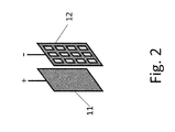
During the process of EPD, surface-charged particles suspended in a liquid medium will migrate under the influence of an external electric field and be deposited onto an electrically conductive or semi-conductive surface, usually charged oppositely to the particles, herein referred to as the “deposition electrode” or substrate. The migration is ultimately caused by the presence of the surface charge of the particles relative to the suspension medium. FIG. 1 is a schematic of an apparatus for carrying an EPD process according to the present invention. An electrical potential is applied across the deposition electrode 11 (e.g. + or − electrode) and the counter electrode 12 (e.g. − or + electrode). Both electrodes 11 and 12 are immersed in a container 13 holding the colloidal suspension, which comprises a plurality of surface-charged nanoparticles 14 (e.g. negatively-charged nanoparticles) and the liquid medium 15. Typically the suspension is stirred during deposition using a stirrer 16. When the nanoparticles 14 gain sufficient kinetic energy from the applied electric field between the electrodes 11 and 12, they will reach the deposition electrode 11 where their charges will be neutralized. The nanoparticles 14 will then be deposited on the deposition electrode 11 and form a close-packed thin film of the same material after the electrode 11 is taken out and dried. FIG. 2 shows a trimetric view of the electrodes, 11 and 12. FIG. 2 also illustrates that the counter electrode 12 may have a shape of a mesh or a grid with hollow center areas, or other shapes, to create the proper electrical field distribution and/or nanoparticle flow density to ensure a uniform deposition on the deposition electrode 11. FIG. 3 shows an alternative apparatus wherein the electrodes 11 and 12 are placed horizontally, which may be an option for manufacturing scale-up.
Generally, nanoparticle materials suitable for an EPD method include, but are not limited, to metals, alloys, semiconductors, ceramics, glass, polymers, or carbon. According to an embodiment of the present invention, and without loss of generality, the absorber layers for use in photovoltaic devices may be made from a mixture of nanoparticles comprising a combination of elements of groups IB, most preferably Cu, and IIIA, and optionally VIA of the periodic table of elements. In another embodiment, the mixture can comprise a combination of elements of groups IB, most preferably Cu, and IIB and/or IVA and optionally VIA elements of the periodic table of elements. The group IB elements preferably include copper (Cu), silver (Ag), or gold (Au). Group IIIA elements suitable for use in the method of this invention include aluminum (Al), gallium (Ga), and indium (In). Preferably the group IIIA elements are Ga and In. Group IIB elements suitable for use in this invention include zinc (Zn), cadmium (Cd), and mercury (Hg). Preferably the group IIB element is Zn. Group IVA elements suitable for use in this invention include silicon (Si), germanium (Ge), tin (Sn) and lead (Pb). Preferably the group IVA element is Si or Sn. Group VIA elements suitable for use in various embodiments include selenium (Se), sulfur (S), and tellurium (Te). For convenience in description, elements that are possibly able to be combined or interchanged are commonly put in a set of parentheses, for example, (Al,Ga,In) or (S,Se,Te). The nanoparticles may contain one material or a mix of two or more materials from elemental metals, binary or ternary alloys, and binary or ternary or quaternary compounds. For convenience, hyphen (“-”) is used to connect elements together and indicates all known binary, ternary, or quaternary alloys or compounds of the elements joined by the hyphen. For example, “Cu—In” indicates all know binary alloys that include both Cu and In elements such as Cu2In, Cu4In, Cu11In9, and the like. Preferably, nanoparticles used in the method of the present invention comprise one or more of the following materials: Cu, Ag, Ag, Al, Ga, In, Zn, Si, Sn, S, Se, Te, Cu—Ag, (Al,Ga)—In, (Cu,Ag)—(Al,In,Ga), (Cu,Ag)—Zn, (Cu,Ag)—(Si,Sn), Zn—(Si,Sn), (Cu,Ag)—(S,Se,Te), (Al,Ga,In)—(S,Se,Te), Zn—(S,Se,Te), (Si,Sn)—(S,Se,Te), (Cu,Ag)—(Al,Ga,In)—(S,Se,Te), (Cu,Ag)—(Si,Sn)—(S,Se,Te), (Cu,Ag)—Zn—(Si,Sn)—(S,Se,Te), and the like. More preferably, the nanoparticles comprise one or more materials selected from binary and ternary alloys of Cu—In, Cu—Ga, In—Ga, (Al,Ga)—In, Cu—(Al,In,Ga), Cu—Zn, Cu—Sn, and Zn—Sn, and binary or ternary or quaternary compounds of Cu—(S,Se), (Al,Ga,In)—(S,Se), Zn—(S,Se), Sn—(S,Se), Cu—(Al,Ga,In)—(S,Se), and Cu—Zn—Sn—(S,Se).
For most applications, the group IB element used in both embodiments is Cu. When selecting materials from the above lists, the atomic ratios or equivalently the molar ratios between the group IB, IIIA, and VIA elements or between group IB and (IIB+IVA) and VIA elements, e.g. Cu:(In+Ga):Se for CIGS and Cu:(Zn+Sn):S for CZTS absorber layers, are carefully adjusted to the predetermined ratio of within a few percent near the ideal chemical composition of the objective photovoltaic absorber layer. Thus, for example, Cu:(In+Ga):Se should have an atomic ratio of approximately 25%:25%:50% and Cu:(Zn+Sn):(S+Se) approximately at 25%:25%:50% plus or minus 15%, most preferably plus or minus 5%. The range of 15% to 5% is required for practical reasons. Loss of, for example, Cu or In or Se during the process, especially considering the high vapor pressure of In—Se compounds and of elemental Se requires that the acceptable ratio ranges be extended to plus or minus 15%. In the case in either embodiment where the optional group VIA elements are not present the ratio of group IB (Cu) to IIA elements is 50%:50% and the ratio of group IB (Cu) to (IIB+IVA) elements is also 50%:50%, both ratios preferably plus or minus 5% and acceptably plus or minus up to 15%.
The nanoparticles may also be prepared as a chemical complex. For example, CIGS nanoparticles may be synthesized through various chemical reaction methods as described in the sonochemical method by H. Zhu, Chem. Mater. 12, 73, (2000); thermolysis described by M. A. Malik et. al. Adv. Mat. 11, 1441 (1999); and pyrolysis described by S. L. Castro et. al. Chem. Mater. 15, 3142 (2003) such that the resultant nanoparticle contains the desired chemical composition.
The nanoparticles may have a plurality of shapes including but not limited to nanospheres, nanorods, nanowires, nanocubes, nanoflowers, nanoflakes, mixtures of these shapes and the like, depending on the bulk material properties and fabrication method. The desired size of the nanoparticles suitable for the method of the present invention ranges between about 1 nm and 500 nm in at least one dimension, preferably between about 1 nm and about 100 nm in at least one dimension. According to an embodiment of this invention, a thin oxide layer may be formed on the surface of the nanoparticle, depending on the particle fabrication method and the liquid medium of the colloidal suspension.
According to an embodiment of the present invention, the nanoparticles are prepared by physical breakdown of bulk source materials, wherein the nanoparticles and the bulk materials have an identical chemical composition. The nanoparticles may be prepared in a preferred liquid medium to form the colloid suspension, or they may be prepared in but not limited to, a vacuum, a gas medium, or a liquid medium, and then re-dispersed in a preferred liquid medium to form the colloid suspension. Methods of preparing the nanoparticles include but are not limited to pulsed laser ablation, laser pyrolysis, arc discharge, thermal evaporation, plasma evaporation, evaporation-condensation, and mechanical ball milling of the bulk material. These methods, indicated as the “physical breakdown methods” suitable for this invention, have an advantage of providing easy controllability of the chemical composition of the nanoparticles by simply adjusting the composition of the source bulk material. In addition, the formation of the bulk material can use a plurality of methods not limited by EPD considerations, and therefore much more complex bulk materials can be prepared. The use of physical breakdown of bulk materials allows the EPD process to have better film quality control, maximizes material usage, and at the same time reduces process complexity. By way of contrast, we use “chemical synthesis methods” to denote the particle preparation methods used in prior art EPD processes of Brown and Salt, and U.S. Pat. Nos. 3,879,276, 4,204,933, 4,225,408, and 4,482,933, and in prior art of other non-vacuum deposition techniques such as the sonochemical reaction described by J J. Zhu, Chem. Mater., 12, 73, (2000), thermolysis described by M. A. Malik et al., Adv. Mat., 11, 1441, (1999), pyrolysis described by S. L. Castro et al., Chem. Mater., 15, 3142, (2003), and spray coprecipitation described in U.S. Pat. No. 7,663,057. In these chemical synthesis methods, compositional control of the synthesized nanoparticles is much more challenging since several reactants/precursors, electrolytes, surfactants/dispersants are employed in the process, and each of them may affect the composition of the deposited film individually. In addition, the inactive part of the reactants/electrolytes, usually the anion part, and the residual by-products, surfactants/dispersants or other additives are typically macromolecular compounds that are difficult to fully decompose, or to be fully eliminated from the final product by post-deposition treatments. In the prior art use of EPD, acids and/or bases are commonly employed for altering the pH value and conductivity of the colloidal suspension, e.g. “Electrophoretic deposition of materials” Van der Biest and Vandeperre, Annu. Rev. Mater. Sci. 29, 327 (1999). The use of acid/base may induce undesirable formation of by-products, such as H2 and O2 gases, at the electrodes, and interfere with the film deposition. Only by incorporating the physical breakdown method of the present invention into the EPD process as stated in this invention, can one effectively avoid undesirable by-product formation, maximize source material usage, and reduce chemical contaminations in the final product of the invention.
A stable suspension of nanoparticles with surface charges is needed for the EPD process according to the present invention. Migration of these nanoparticles driven by a strong electric force is recognized to be of a physical nature rather than of a chemical nature. The nanoparticles may have a positive surface charge or a negative surface charge depending on the nature of the liquid medium and on the bulk materials from which the nanoparticles are formed. According to an embodiment of the present invention, preferably the surface-charged nanoparticles in a stable suspension have an absolute value of zeta potential greater than 10 milliVolts (mV). Zeta potential (ζ) is used to represent the degree of repulsion between adjacent surface-charged nanoparticles. It is determined from the velocity (ν) with which the nanoparticle moves under an electric field (E) according to the following equation: ζ=(4πην)/(∈E), where η and ∈ are the viscosity and dielectric constant of the liquid medium, respectively.
The liquid medium of the colloidal suspension may be one solvent or a mixture of two or more solvents, wherein the solvents include but are not limited to, water and water-miscible organic liquids, preferably single phase polar organic liquids. The polar organic liquid may have a large dielectric constant of more than 10, and more preferably of more than 20. General classes of the polar organic liquids suitable for this invention include but are not limited to, alcohols, ethers, ketones, esters, amides, nitriles, and diols, and the like. Preferably the formula of the polar organic liquid contains 1-6 carbon atoms. In some embodiments, a non-aqueous medium is preferred over an aqueous medium, to avoid potential electrolysis of water and gas formation at the electrodes, which may interfere with the deposition process.
Some embodiments may employ one or more suitable additives to improve the stability and conductivity of the colloidal suspension, or to improve adhesion of the deposited photovoltaic absorber layer at the absorber layer/substrate interface. Such additives include but are not limited to, acids, bases, electrolytes, and surfactants/dispersants which are well known in the colloidal art. However, in various embodiments, such additives should be removable from the absorber layer during or after deposition. Particularly, additives are chosen to ensure that they do not disadvantage the process or the product of the invention.
Generally, the substrate on which the absorber layer is deposited is electrically conductive or semi-conductive, and is directly connected to or is the deposition electrode, wherein the deposition surface faces the counter electrode. The polarity of the deposition electrode, either positive or negative, is determined as an opposite charge to the charge polarity of the nanoparticles. The substrate also acts as the bottom contact in a photovoltaic device. It may be in the form of, but is not limited to: (1) a rigid sheet of glass with a conductive coating, preferably a metal coating and more preferably a molybdenum coating; (2) a flexible sheet of a metal or an alloy, including but not limited to molybdenum, titanium, stainless steel, or aluminum, with or without additional coatings; or (3) a flexible polymeric sheet having a conductive coating, preferably a metal coating and more preferably a molybdenum coating. The suitable polymers for forming the polymeric sheet include, but are not limited to, polyimides, polyethylene terephthalate, or polyethersulphone. In embodiments wherein a metal or an alloy substrate is used, it would be desirable but not necessary to cover the backside of the substrate with a blocking material such as an insulating tape or membrane to inhibit useless deposition on the back side of the substrate. It would also be desirable to pre-coat a thin layer of molybdenum and/or an intermediate blocking layer on the metal sheet to improve adhesion and inhibit interdiffusion between the metal substrate and the deposited film as described in U.S. patent publication no. 2009/0305455.
The counter electrode is typically made of either a conductive metal or a conductive alloy, including but not limited to, stainless steel, molybdenum, nickel, titanium, platinum, gold, or a metal-coated glass sheet. Unlike the deposition electrode substrate, which is typically in planar shape for photovoltaic applications, the shape of the counter electrode may be deliberately altered to change the electric field distribution. When the counter electrode is also a planar sheet, although the electric field between planar electrodes is uniform, the deposited film is usually non-uniform, e.g. thinner at the center and thicker at the edge of the substrate. This phenomenon is more apparent when the distance between the two electrodes is decreased to obtain a stronger electrical field. This phenomenon is due to the small spacing limiting the number of nanoparticles that are able to migrate to the center of the substrate for deposition. To ensure uniform coating on the deposition electrode, the counter electrode may be configured in the form of a mesh or a sheet with hollow center areas. FIG. 2 illustrates one embodiment of the current invention wherein a counter electrode with rectangular-shaped holes is employed.
The voltage applied to the electrodes, the distance between the electrodes, and the current density employed on the electrodes may be configured in light of the intensity of the electric field required for the deposition of the nanoparticles. Depending on the nanoparticle properties and electrode size, the applied voltage may be direct current (DC) or alternating current (AC) and may be either continuous or pulsed. The electrical potential is preferably from 1 to 1000 Volts (V), more preferably from 50 to 500 V. The distance between the electrodes is preferably from 0.1 to 100 centimeters (cm), more preferably from 0.5 to 10 cm. The current density is preferably from 0.001 to 10 milliAmps/centimeter2 (mA/cm2), more preferably from 0.01 to 1 mA/cm2.
The deposition speed is determined by the operating parameters. In some embodiments, a 0.5 to 2 micron (μm) thick film with a good packing density may be deposited by the current method in a short time of from 30 seconds to 5 minutes. The deposition speed of the current method is much faster than the conventional vacuum-based techniques, and is among the fastest compared to other non-vacuum-based techniques in terms of depositing a thin film photovoltaic absorber layer with similar packing density.
According to an embodiment of the present invention, virtually all of the nanoparticles in the liquid medium may be deposited under an optimized configuration of the EPD process onto the substrate. Thus, the material usage is much more efficient in the current method compared to the conventional vacuum-based and other non-vacuum-based techniques. Therefore, the current method helps to reduce the environmental footprint of the process of forming a photovoltaic absorber layer.
By way of an example, FIG. 4 displays a cross-sectional scanning electron microscopy image of a Cu—In alloy film of 1.5 μm thickness deposited on a molybdenum coated glass substrate according to the current method. Pulsed laser ablation was employed to generate the Cu—In alloy nanoparticles in acetone. The laser pulse repetition rate was preferably about 500 kilo-Hertz. The pulse energy was preferably about 8 micro-Joule. The ultrashort laser pulse duration is preferably between 0.1 to 1 picosecond. The target ablated by the laser was a commercial sputtering target purchased form SCI Engineering Materials Inc. containing 50% Cu and 50% In. The size of the ablated nanoparticles ranged between about 1 nm and 500 nm in diameter. The nanoparticles were deposited by EPD under an applied DC voltage of about 400 V, with a current density of about 0.2 mA/cm2. The distance between the electrodes was about 1 cm. To qualify for photovoltaic application, the film deposited by the current method generally requires further post-deposition treatment of chalcogenization, including but not limited to selenization or sulfurization or tellurization, and/or annealing as illustrated in the flow chart of FIG. 5 . Chalcogenization will transform the initially deposited absorber layer into an absorber layer with the desired structure of a chalcopyrite or a kesterite, or improve the film structural quality and optical and electrical properties if the initially deposited layer already has the desired structure. By way of an example, the film may be selenized by exposing the layer to a selenium vapor at a temperature of between 400 and 550° C. for 5 to 60 minutes.
The method for fabricating a photovoltaic absorber layer according to the present invention has excellent reproducibility and stability. The present invention may also be used to fabricate other devices including photodetectors, photoelectrochemical cells, solid oxide fuel cells, supercapacitors, ceramic matrix/fiber composites and other energy conversion or energy storage devices.
The foregoing invention has been described in accordance with the relevant legal standards, thus the description is exemplary rather than limiting in nature. Variations and modifications to the disclosed embodiment may become apparent to those skilled in the art and do come within the scope of the invention. Accordingly, the scope of legal protection afforded this invention can only be determined by studying the following claims.
Claims (23)
1. A method for fabricating a thin film photovoltaic absorber layer comprising the steps of:
a) providing nanoparticles comprising a combination of either Cu and one or more group IIIA elements, and optionally one or more group VIA elements or a combination of Cu and one or more group IIB and one or more group IVA elements, and optionally one or more group VIA elements of the periodic table, wherein further comprises forming the nanoparticles by a physical breakdown of a bulk material and wherein the nanoparticles have an identical atomic ratio between the elements as the bulk material;
b) preparing a colloidal suspension of a mixture of the nanoparticles in a liquid medium, wherein the atomic ratio between Cu and group IIIA and optional group VIA elements and between Cu and group IIB and group IVA elements and optional group VIA elements are predetermined; and
c) submerging a substrate and a counter electrode into the colloidal suspension and depositing the mixture of nanoparticles onto the substrate to form a thin film photovoltaic absorber layer by electrophoretic deposition, wherein the predetermined atomic ratio between Cu and group IIIA and optional group VIA elements or between Cu and (group IIB plus group IVA elements) and optional group VIA elements is 25%:25%:50% plus or minus 15%.
2. The method of claim 1 wherein step a) comprises providing nanoparticles selected from the group consisting of copper (Cu), indium (In), aluminum (Al), gallium (Ga) selenium (Se), and sulfur (S).
3. The method of claim 1 wherein step a) comprises providing nanoparticles selected from the group consisting of copper (Cu), zinc (Zn), tin (Sn), selenium (Se), and sulfur (S).
4. The method of claim 1 wherein step a) comprises providing nanoparticles comprising one or more materials selected from the group consisting of binary or ternary alloys of Cu—In, Cu—Ga, In—Ga, (Al,Ga)—In, Cu—(Al,In,Ga), Cu—Zn, Cu—Sn, Zn—Sn, and from binary, ternary, or quaternary compounds of Cu—(S,Se), (Al,Ga,In)—(S,Se), Zn—(S,Se), Sn—(S,Se), Cu—(Al,Ga,In)—(S,Se), and Cu—Zn—Sn—(S,Se).
5. The method of claim 1 wherein the nanoparticles are formed by pulsed laser ablation of the bulk material.
6. The method of claim 1 wherein the nanoparticles are formed by thermal evaporation of the bulk material.
7. The method of claim 1 wherein the nanoparticles are formed by arc discharge of the bulk material.
8. The method of claim 1 wherein the nanoparticles are formed by plasma evaporation of the bulk material.
9. The method of claim 1 wherein the nanoparticles are formed by mechanical ball milling of the bulk material.
10. The method of claim 1 wherein step a) comprises providing nanoparticles having shapes of a nanosphere, a nanorod, a nanowire, a nanocube, a nanoflower, a nanoflake, or mixtures thereof.
11. The method of claim 1 wherein step a) comprises providing nanoparticles having at least one dimension that is 500 nanometers or less.
12. The method of claim 11 wherein step a) comprises providing nanoparticles having at least one dimension that is 100 nanometers or less.
13. The method of claim 1 wherein step a) comprises providing nanoparticles that have been formed in at least one of a vacuum, a gas medium, or a liquid medium.
14. The method of claim 1 wherein step b) comprises selecting a liquid medium comprising water.
15. The method of claim 1 wherein step b) comprises selecting a liquid medium comprising at least one water-miscible organic solvent having 1-6 carbon atoms and a dielectric constant of more than 10.
16. The method of claim 1 wherein step b) comprises selecting a liquid medium comprising at least one water-miscible organic solvent having 1-6 carbon atoms and a dielectric constant of more than 20.
17. The method of claim 1 wherein step b) further comprises adding to the liquid medium at least one of an acid, a base, an electrolyte, a surfactant, and a dispersant.
18. The method of claim 1 wherein step c) comprises selecting as the substrate one of a sheet of glass with a conductive coating on it; a polymeric sheet with a conductive coating on it; or a sheet comprising at least one of molybdenum, titanium, stainless steel, or aluminum, with or without additional coatings on it.
19. The method of claim 1 wherein step c) further comprises covering a backside of the substrate with a blocking material.
20. The method of claim 19 further comprising selecting as the blocking material a material comprising an insulating tape or membrane.
21. The method of claim 1 wherein step c) comprises selecting as the counter electrode one made of a metal, an alloy, or a metal-coated glass.
22. The method of claim 1 wherein step c) comprises selecting as the counter electrode one that is in the form of a planar sheet, a mesh, or a sheet with hollow center areas.
23. The method of claim 1 further comprising the step of subjecting the thin film photovoltaic absorber layer to one or more steps of chalcogenization and annealing.
Priority Applications (4)
| Application Number | Priority Date | Filing Date | Title |
|---|---|---|---|
| US12/910,929 US8409906B2 (en) | 2010-10-25 | 2010-10-25 | Non-vacuum method for fabrication of a photovoltaic absorber layer |
| US13/053,441 US20120100660A1 (en) | 2010-10-25 | 2011-03-22 | Method for preparation of metal chalcogenide solar cells on complexly shaped surfaces |
| US13/198,744 US8748216B2 (en) | 2010-10-25 | 2011-08-05 | Non-vacuum method for fabrication of a photovoltaic absorber layer |
| PCT/US2011/057000 WO2012061023A1 (en) | 2010-10-25 | 2011-10-20 | A non-vacuum method for fabrication of a photovoltaic absorber layer |
Applications Claiming Priority (1)
| Application Number | Priority Date | Filing Date | Title |
|---|---|---|---|
| US12/910,929 US8409906B2 (en) | 2010-10-25 | 2010-10-25 | Non-vacuum method for fabrication of a photovoltaic absorber layer |
Related Parent Applications (1)
| Application Number | Title | Priority Date | Filing Date |
|---|---|---|---|
| US13/053,441 Continuation US20120100660A1 (en) | 2010-10-25 | 2011-03-22 | Method for preparation of metal chalcogenide solar cells on complexly shaped surfaces |
Related Child Applications (2)
| Application Number | Title | Priority Date | Filing Date |
|---|---|---|---|
| US13/053,441 Continuation-In-Part US20120100660A1 (en) | 2010-10-25 | 2011-03-22 | Method for preparation of metal chalcogenide solar cells on complexly shaped surfaces |
| US13/198,744 Continuation-In-Part US8748216B2 (en) | 2010-10-25 | 2011-08-05 | Non-vacuum method for fabrication of a photovoltaic absorber layer |
Publications (2)
| Publication Number | Publication Date |
|---|---|
| US20120097224A1 US20120097224A1 (en) | 2012-04-26 |
| US8409906B2 true US8409906B2 (en) | 2013-04-02 |
Family
ID=45971928
Family Applications (1)
| Application Number | Title | Priority Date | Filing Date |
|---|---|---|---|
| US12/910,929 Expired - Fee Related US8409906B2 (en) | 2010-10-25 | 2010-10-25 | Non-vacuum method for fabrication of a photovoltaic absorber layer |
Country Status (1)
| Country | Link |
|---|---|
| US (1) | US8409906B2 (en) |
Cited By (4)
| Publication number | Priority date | Publication date | Assignee | Title |
|---|---|---|---|---|
| US20100180523A1 (en) * | 2007-04-06 | 2010-07-22 | Certainteed Corporation | Photovoltaic Roof Covering |
| US20120098032A1 (en) * | 2010-10-25 | 2012-04-26 | Wei Guo | Non-vacuum method for fabrication of a photovoltaic absorber layer |
| US20130171768A1 (en) * | 2011-12-30 | 2013-07-04 | Tsung-Shin Wu | Fabriation method for light absorption layer of solar cell |
| US10483532B2 (en) | 2012-08-07 | 2019-11-19 | Cornell University | Binder-free and carbon-free nanoparticle containing component, methods and applications |
Families Citing this family (4)
| Publication number | Priority date | Publication date | Assignee | Title |
|---|---|---|---|---|
| WO2013019299A2 (en) * | 2011-05-11 | 2013-02-07 | Qd Vision, Inc. | Method for processing devices including quantum dots and devices |
| WO2014052901A2 (en) * | 2012-09-29 | 2014-04-03 | Precursor Energetics, Inc. | Processes for photovoltaic absorbers with compositional gradients |
| JP6366914B2 (en) | 2013-09-24 | 2018-08-01 | 株式会社東芝 | Multi-junction solar cell |
| EP3158364A1 (en) * | 2014-06-23 | 2017-04-26 | Rensselaer Polytechnic Institute | Fabricating radiation-detecting structures |
Citations (32)
| Publication number | Priority date | Publication date | Assignee | Title |
|---|---|---|---|---|
| US3879276A (en) | 1974-04-10 | 1975-04-22 | Int Standard Electric Corp | Electrophoretic deposition of selenium |
| US4204933A (en) | 1977-11-15 | 1980-05-27 | Imperial Chemical Industries Limited | Electrocoating process for producing a semiconducting film |
| US4225408A (en) | 1976-05-17 | 1980-09-30 | Imperial Chemical Industries Limited | Process for electrolytically preparing a semiconducting film on a flexible substrate |
| US4482933A (en) | 1981-07-30 | 1984-11-13 | Itt Industries, Inc. | Multilayer doped ceramic capacitor |
| US4482447A (en) | 1982-09-14 | 1984-11-13 | Sony Corporation | Nonaqueous suspension for electrophoretic deposition of powders |
| WO1988010513A1 (en) | 1987-06-26 | 1988-12-29 | Prutec Limited | Manufacture of solar cells |
| US5660746A (en) | 1994-10-24 | 1997-08-26 | University Of South Florida | Dual-laser process for film deposition |
| US5756924A (en) | 1995-09-28 | 1998-05-26 | The Regents Of The University Of California | Multiple laser pulse ignition method and apparatus |
| US6060128A (en) | 1997-03-25 | 2000-05-09 | The Board Of Trustees Of The University Of Illinois | Method of producing thin film and nanoparticle deposits using charges of alternating polarity |
| WO2004019420A1 (en) | 2002-08-16 | 2004-03-04 | Daimlerchrysler Ag | Body part of a vehicle provided with a thin-film solar cell and the production thereof |
| US6783569B2 (en) | 2001-08-16 | 2004-08-31 | Korea Advanced Institute Of Science And Technology | Method for synthesis of core-shell type and solid solution alloy type metallic nanoparticles via transmetalation reactions and applications of same |
| US20050226287A1 (en) | 2004-03-31 | 2005-10-13 | Imra America, Inc. | Femtosecond laser processing system with process parameters, controls and feedback |
| US20050243396A1 (en) | 2004-04-12 | 2005-11-03 | Mitsumi Fujii | Deflector mirror, optical scanning device, and image forming apparatus |
| US20050276931A1 (en) | 2004-06-09 | 2005-12-15 | Imra America, Inc. | Method of fabricating an electrochemical device using ultrafast pulsed laser deposition |
| US20060086834A1 (en) | 2003-07-29 | 2006-04-27 | Robert Pfeffer | System and method for nanoparticle and nanoagglomerate fluidization |
| US20070029185A1 (en) | 2005-08-08 | 2007-02-08 | Hon Hai Precision Industry Co., Ltd. | Apparatus for producing nanoparticles |
| US20070051202A1 (en) | 2005-09-02 | 2007-03-08 | The Curators Of The University Of Missouri. | Methods and articles for gold nanoparticle production |
| US7235736B1 (en) | 2006-03-18 | 2007-06-26 | Solyndra, Inc. | Monolithic integration of cylindrical solar cells |
| US7306823B2 (en) | 2004-09-18 | 2007-12-11 | Nanosolar, Inc. | Coated nanoparticles and quantum dots for solution-based fabrication of photovoltaic cells |
| US20080041532A1 (en) | 2006-08-07 | 2008-02-21 | Industrial Technology Research Institute | System for fabricating nanoparticles |
| WO2009117451A1 (en) | 2008-03-21 | 2009-09-24 | Imra America, Inc. | Laser-based material processing methods and systems |
| US20090246413A1 (en) | 2008-03-27 | 2009-10-01 | Imra America, Inc. | Method for fabricating thin films |
| US20090246530A1 (en) | 2008-03-27 | 2009-10-01 | Imra America, Inc. | Method For Fabricating Thin Films |
| US7604843B1 (en) | 2005-03-16 | 2009-10-20 | Nanosolar, Inc. | Metallic dispersion |
| US20090305455A1 (en) | 2004-09-18 | 2009-12-10 | Craig Leidholm | Formation of CIGS Absorber Layers on Foil Substrates |
| WO2010017124A2 (en) | 2008-08-04 | 2010-02-11 | Sunlight Photonics Inc. | A reacted particle deposition (rpd) method for forming a compound semi-conductor thin-film |
| US7663057B2 (en) | 2004-02-19 | 2010-02-16 | Nanosolar, Inc. | Solution-based fabrication of photovoltaic cell |
| US20100133479A1 (en) | 2008-12-03 | 2010-06-03 | Industrial Technology Research Institute | Fabrication method for ibiiiavia-group amorphous compound and ibiiiavia-group amorphous precursor for thin-film solar cells |
| US20100196192A1 (en) | 2009-01-30 | 2010-08-05 | Imra America, Inc. | Production of metal and metal-alloy nanoparticles with high repetition rate ultrafast pulsed laser ablation in liquids |
| US20100248419A1 (en) | 2009-02-15 | 2010-09-30 | Jacob Woodruff | Solar cell absorber layer formed from equilibrium precursor(s) |
| US20100242800A1 (en) | 2009-03-25 | 2010-09-30 | Chuan-Lung Chuang | Method For Preparing Sol-Gel Solution For CIGS Solar Cell |
| US20110192714A1 (en) | 2010-02-10 | 2011-08-11 | Bing Liu | Nanoparticle production in liquid with multiple-pulse ultrafast laser ablation |
-
2010
- 2010-10-25 US US12/910,929 patent/US8409906B2/en not_active Expired - Fee Related
Patent Citations (35)
| Publication number | Priority date | Publication date | Assignee | Title |
|---|---|---|---|---|
| US3879276A (en) | 1974-04-10 | 1975-04-22 | Int Standard Electric Corp | Electrophoretic deposition of selenium |
| US4225408A (en) | 1976-05-17 | 1980-09-30 | Imperial Chemical Industries Limited | Process for electrolytically preparing a semiconducting film on a flexible substrate |
| US4204933A (en) | 1977-11-15 | 1980-05-27 | Imperial Chemical Industries Limited | Electrocoating process for producing a semiconducting film |
| US4482933A (en) | 1981-07-30 | 1984-11-13 | Itt Industries, Inc. | Multilayer doped ceramic capacitor |
| US4482447A (en) | 1982-09-14 | 1984-11-13 | Sony Corporation | Nonaqueous suspension for electrophoretic deposition of powders |
| WO1988010513A1 (en) | 1987-06-26 | 1988-12-29 | Prutec Limited | Manufacture of solar cells |
| EP0297799A1 (en) | 1987-06-26 | 1989-01-04 | Prutec Limited | Manufacture of Solar Cells |
| US5660746A (en) | 1994-10-24 | 1997-08-26 | University Of South Florida | Dual-laser process for film deposition |
| US5756924A (en) | 1995-09-28 | 1998-05-26 | The Regents Of The University Of California | Multiple laser pulse ignition method and apparatus |
| US6060128A (en) | 1997-03-25 | 2000-05-09 | The Board Of Trustees Of The University Of Illinois | Method of producing thin film and nanoparticle deposits using charges of alternating polarity |
| US6783569B2 (en) | 2001-08-16 | 2004-08-31 | Korea Advanced Institute Of Science And Technology | Method for synthesis of core-shell type and solid solution alloy type metallic nanoparticles via transmetalation reactions and applications of same |
| US20060037641A1 (en) | 2002-08-16 | 2006-02-23 | Horst Kibbel | Body part of a vehicle provided with a thin-film solar cell and the production thereof |
| EP1529314A1 (en) | 2002-08-16 | 2005-05-11 | DaimlerChrysler AG | Body part of a vehicle provided with a thin-film solar cell and the production thereof |
| WO2004019420A1 (en) | 2002-08-16 | 2004-03-04 | Daimlerchrysler Ag | Body part of a vehicle provided with a thin-film solar cell and the production thereof |
| US20060086834A1 (en) | 2003-07-29 | 2006-04-27 | Robert Pfeffer | System and method for nanoparticle and nanoagglomerate fluidization |
| US7663057B2 (en) | 2004-02-19 | 2010-02-16 | Nanosolar, Inc. | Solution-based fabrication of photovoltaic cell |
| US20050226287A1 (en) | 2004-03-31 | 2005-10-13 | Imra America, Inc. | Femtosecond laser processing system with process parameters, controls and feedback |
| US20050243396A1 (en) | 2004-04-12 | 2005-11-03 | Mitsumi Fujii | Deflector mirror, optical scanning device, and image forming apparatus |
| US20050276931A1 (en) | 2004-06-09 | 2005-12-15 | Imra America, Inc. | Method of fabricating an electrochemical device using ultrafast pulsed laser deposition |
| US20090305455A1 (en) | 2004-09-18 | 2009-12-10 | Craig Leidholm | Formation of CIGS Absorber Layers on Foil Substrates |
| US7306823B2 (en) | 2004-09-18 | 2007-12-11 | Nanosolar, Inc. | Coated nanoparticles and quantum dots for solution-based fabrication of photovoltaic cells |
| US7604843B1 (en) | 2005-03-16 | 2009-10-20 | Nanosolar, Inc. | Metallic dispersion |
| US20070029185A1 (en) | 2005-08-08 | 2007-02-08 | Hon Hai Precision Industry Co., Ltd. | Apparatus for producing nanoparticles |
| US20070051202A1 (en) | 2005-09-02 | 2007-03-08 | The Curators Of The University Of Missouri. | Methods and articles for gold nanoparticle production |
| US7235736B1 (en) | 2006-03-18 | 2007-06-26 | Solyndra, Inc. | Monolithic integration of cylindrical solar cells |
| US20080041532A1 (en) | 2006-08-07 | 2008-02-21 | Industrial Technology Research Institute | System for fabricating nanoparticles |
| WO2009117451A1 (en) | 2008-03-21 | 2009-09-24 | Imra America, Inc. | Laser-based material processing methods and systems |
| US20090246413A1 (en) | 2008-03-27 | 2009-10-01 | Imra America, Inc. | Method for fabricating thin films |
| US20090246530A1 (en) | 2008-03-27 | 2009-10-01 | Imra America, Inc. | Method For Fabricating Thin Films |
| WO2010017124A2 (en) | 2008-08-04 | 2010-02-11 | Sunlight Photonics Inc. | A reacted particle deposition (rpd) method for forming a compound semi-conductor thin-film |
| US20100133479A1 (en) | 2008-12-03 | 2010-06-03 | Industrial Technology Research Institute | Fabrication method for ibiiiavia-group amorphous compound and ibiiiavia-group amorphous precursor for thin-film solar cells |
| US20100196192A1 (en) | 2009-01-30 | 2010-08-05 | Imra America, Inc. | Production of metal and metal-alloy nanoparticles with high repetition rate ultrafast pulsed laser ablation in liquids |
| US20100248419A1 (en) | 2009-02-15 | 2010-09-30 | Jacob Woodruff | Solar cell absorber layer formed from equilibrium precursor(s) |
| US20100242800A1 (en) | 2009-03-25 | 2010-09-30 | Chuan-Lung Chuang | Method For Preparing Sol-Gel Solution For CIGS Solar Cell |
| US20110192714A1 (en) | 2010-02-10 | 2011-08-11 | Bing Liu | Nanoparticle production in liquid with multiple-pulse ultrafast laser ablation |
Non-Patent Citations (20)
| Title |
|---|
| A. Pyatenko et al., "Synthesis of silver nanoparticles by laser ablation in pure water", A. Pyatenko et al., Applied Physics A, vol. 79, 2004, pp. 803-806. |
| A.V. Simaken et al., "Nanodisks of Au and Ag produced by laser ablation in liquid environment", Chemical Physics Letters vol. 348, 2001, pp. 182-186. |
| Brown et al.: "The mechanism of electrophoretic deposition" J. Appl. Chem., 15, 40 (1965). |
| C.P. Chan et al., "Preparation of Cu2ZnSnS4 Film by Electrodeposition Using Ionic Liquids" Solar Energy Materials and Solar Cells, 94207 (2010). |
| D. F. Huessy at al., "Water, Ultrapure" in Ullmann's Ency. Of Industrial Chemistry, Pub. Oct. 15, 2008, 26 pgs. |
| D.L. Schulz et al., Cu-In-Ga-Se Nanoparticle Colloids as Spray Deposition Precursors for Cu(In,Ga) Se2 Solar Cell Materials, 27(5), 433-437 (1998). |
| I. Lee et al., "Production of Au-Ag alloy nanoparticles by laser ablation of bulk alloys", Chemical Communications, 2001, pp. 1782-1783. |
| International Search Report; 3 Pages Dated Feb. 6, 2012. |
| J. Brannon et al.," Laser Processing for Microengineering Applications", Chp 5 in Microengineering Aerospace Systems, editor: H. Helvajian, copyright 1999, pp. 145, 160-162, 187 and 188. |
| JJ. Zhu, "General Sonochemical Method for the Preparation of Nanophasic Selenides: Synthesis of ZnSe Nanoparticles" Chem. Mater., 12, 73, (2000). |
| M. A. Malik et. al.: "A Novel Route for the Preparation of CuSe and CuInSe2 Nanoparticles" Adv. Mat. 11, 1441 (1999). |
| M. Kaelin, et al., "CIS and CIGS Layers from Selenized Nanoparticle Precursors" Thin Solid Films, 431-43258 (2003). |
| S. Anh et al., "Effects of Selenization Conditions on Densification of Cu(In, Ga)Se2 (CIGS) Thin Films Prepared by Spray Deposition of CIGS Nanoparticles" Journel of Applied Physics, 105113533 (2009). |
| S. Anh et al., "Nanoparticle Derived Cu(In, Ga)Se2 Absorber Layer for Thin Film Solar Cells" Colloids and Surfaces, 313-314171 (2008). |
| S. Barcikowski et al., "Generation of nanoparticle colloids by picosecond and femtosecond laser ablations in liquid flow", Applied Physics Letters, vol. 91, 2007, 083113. |
| S. L. Castro et. al.: Nanocrystalline Chalcopyrite Materials (CuInS2 and CuInSe2) via Low-Temperature Pyrolysis of Molecular Single-Source Precursors, Chem. Mater. 15, 3142 (2003). |
| V.K. Kapur et al., "Non-Vacuum Processing of CuIn1-xGaxSe2 Solar Cells on Rigid and Flexible Substrates Using Nanoparticle Precursor Inks" Thin Solid Films, 431-253 (2003). |
| Van der Biest et al: "Electrophoretic deposition of materials" Annu. Rev. Mater. Sci. 29, 327 (1999). |
| W. E. Nichols et al., "Laser Ablation of a platinum target in water. I. Ablations mechanisms", J of Applied Physics vol. 100, 2006, 114911. |
| Yang, Li, Chapter 2, "Liquid-Phase Pulsed Laser Ablation" in Self-assemble and Ordering Nanomaterials by Liquid-Phased Pulsed Laser Ablation, Dissertation, Nov. 2007 pp. 33-51. |
Cited By (7)
| Publication number | Priority date | Publication date | Assignee | Title |
|---|---|---|---|---|
| US20100180523A1 (en) * | 2007-04-06 | 2010-07-22 | Certainteed Corporation | Photovoltaic Roof Covering |
| US8671630B2 (en) * | 2007-04-06 | 2014-03-18 | Certainteed Corporation | Photovoltaic roof covering |
| US20120098032A1 (en) * | 2010-10-25 | 2012-04-26 | Wei Guo | Non-vacuum method for fabrication of a photovoltaic absorber layer |
| US8748216B2 (en) * | 2010-10-25 | 2014-06-10 | Imra America, Inc. | Non-vacuum method for fabrication of a photovoltaic absorber layer |
| US20130171768A1 (en) * | 2011-12-30 | 2013-07-04 | Tsung-Shin Wu | Fabriation method for light absorption layer of solar cell |
| US8828767B2 (en) * | 2011-12-30 | 2014-09-09 | Industrial Technology Research Institute | Fabriation method for light absorption layer of solar cell |
| US10483532B2 (en) | 2012-08-07 | 2019-11-19 | Cornell University | Binder-free and carbon-free nanoparticle containing component, methods and applications |
Also Published As
| Publication number | Publication date |
|---|---|
| US20120097224A1 (en) | 2012-04-26 |
Similar Documents
| Publication | Publication Date | Title |
|---|---|---|
| US8748216B2 (en) | Non-vacuum method for fabrication of a photovoltaic absorber layer | |
| US8409906B2 (en) | Non-vacuum method for fabrication of a photovoltaic absorber layer | |
| US8206616B2 (en) | Solution-based fabrication of photovoltaic cell | |
| US20120100660A1 (en) | Method for preparation of metal chalcogenide solar cells on complexly shaped surfaces | |
| US9263610B2 (en) | Electrochemical method of producing copper indium gallium diselenide (CIGS) solar cells | |
| Wu et al. | Polytypic nanocrystals of Cu-based ternary chalcogenides: colloidal synthesis and photoelectrochemical properties | |
| Hao et al. | A novel semiconductor-sensitized solar cell based on P3HT@ CdS@ TiO2 core-shell nanotube array | |
| Guo et al. | Liquid-phase pulsed laser ablation and electrophoretic deposition for chalcopyrite thin-film solar cell application | |
| JP3681870B2 (en) | Method for producing compound semiconductor film and solar cell | |
| Badkoobehhezaveh et al. | Electrophoretic behavior of solvothermal synthesized anion replaced Cu2ZnSn (SxSe1-x) 4 films for photoelectrochemical water splitting | |
| Badgujar et al. | Sonochemical synthesis of CuIn0. 7Ga0. 3Se2 nanoparticles for thin film photo absorber application | |
| Dey et al. | Enhanced charge carrier generation by dielectric nanomaterials for quantum dots solar cells based on CdS-TiO2 photoanode | |
| Anand et al. | Electro Synthesised NiTe2 Thin Films with the Influence of Additives | |
| Londhe et al. | Electrochemically synthesized CuInSe2 thin films from non-aqueous electrolyte for solar cell applications | |
| Rohom et al. | Agitation dependent properties of copper indium diselenide thin films prepared by electrochemical route | |
| Londhe et al. | Improvement in the CIGS solar cell parameters by using plasmonic (Au) nanoparticle | |
| Rashid et al. | Influence of electrochemical deposition parameters on morphological properties of ZnO on Si (100) | |
| Kun et al. | Preparation of Cu2ZnSnS4 nanoparticles by laser ablation in liquid and characterization | |
| Turkdogan | A Facile Growth of Cu2ZnSnS4/ZnS Materials by Sulfurization of Stacked Co-Electroplated-Annealed Metallic Film (s) for Photovoltaic Applications | |
| Ukarande et al. | Role of complexing agent on the properties of CdS thin films | |
| Guo et al. | Electrophoretic deposition of Cu-In composite nanoparticle thin films for fabrication of CuInSe [sub] 2 [/sub] solar cells | |
| Petrović et al. | Methodologies Used for the Synthesis of Cuprous Oxide as an Active Solar Cell Material | |
| Guo et al. | Electrophoretic deposition of colloidal nanoparticles for synthesis of chalcopyrite thin films | |
| Abulikemu | Synthesis and Characterization of Colloidal Metal and Photovoltaic Semiconductor Nanocrystals | |
| Guo et al. | Synthesis and electrophoretic deposition of composite metal nanoparticles and non-vacuum fabrication of CuInSe2 solar cells |
Legal Events
| Date | Code | Title | Description |
|---|---|---|---|
| AS | Assignment |
Owner name: IMRA AMERICA, INC., MICHIGAN Free format text: ASSIGNMENT OF ASSIGNORS INTEREST;ASSIGNORS:GUO, WEI;JIN, YU;LIU, BING;AND OTHERS;SIGNING DATES FROM 20101104 TO 20101109;REEL/FRAME:025336/0745 |
|
| REMI | Maintenance fee reminder mailed | ||
| LAPS | Lapse for failure to pay maintenance fees | ||
| STCH | Information on status: patent discontinuation |
Free format text: PATENT EXPIRED DUE TO NONPAYMENT OF MAINTENANCE FEES UNDER 37 CFR 1.362 |
|
| FP | Lapsed due to failure to pay maintenance fee |
Effective date: 20170402 |