US8258480B2 - High energy photon detection using pulse width modulation - Google Patents
High energy photon detection using pulse width modulation Download PDFInfo
- Publication number
- US8258480B2 US8258480B2 US12/397,195 US39719509A US8258480B2 US 8258480 B2 US8258480 B2 US 8258480B2 US 39719509 A US39719509 A US 39719509A US 8258480 B2 US8258480 B2 US 8258480B2
- Authority
- US
- United States
- Prior art keywords
- time
- signal
- energy
- detector
- peak
- Prior art date
- Legal status (The legal status is an assumption and is not a legal conclusion. Google has not performed a legal analysis and makes no representation as to the accuracy of the status listed.)
- Active, expires
Links
- 238000001514 detection method Methods 0.000 title claims description 17
- 230000003993 interaction Effects 0.000 claims abstract description 44
- 238000000034 method Methods 0.000 claims abstract description 33
- 238000012545 processing Methods 0.000 claims abstract description 16
- 230000004044 response Effects 0.000 claims abstract description 8
- 238000003384 imaging method Methods 0.000 claims description 15
- 238000007493 shaping process Methods 0.000 claims description 13
- 230000003287 optical effect Effects 0.000 claims description 9
- 230000001419 dependent effect Effects 0.000 claims description 6
- 230000008878 coupling Effects 0.000 claims description 4
- 238000010168 coupling process Methods 0.000 claims description 4
- 238000005859 coupling reaction Methods 0.000 claims description 4
- 238000002595 magnetic resonance imaging Methods 0.000 claims description 4
- 238000002600 positron emission tomography Methods 0.000 description 25
- 239000003990 capacitor Substances 0.000 description 16
- 230000008901 benefit Effects 0.000 description 8
- 238000001228 spectrum Methods 0.000 description 8
- 238000012360 testing method Methods 0.000 description 8
- 238000013461 design Methods 0.000 description 7
- 230000005540 biological transmission Effects 0.000 description 6
- 239000013078 crystal Substances 0.000 description 6
- 238000001914 filtration Methods 0.000 description 4
- 230000006870 function Effects 0.000 description 4
- 230000000630 rising effect Effects 0.000 description 4
- 239000004065 semiconductor Substances 0.000 description 4
- 230000015556 catabolic process Effects 0.000 description 3
- 230000007123 defense Effects 0.000 description 3
- 238000006731 degradation reaction Methods 0.000 description 3
- 238000005553 drilling Methods 0.000 description 3
- 238000012986 modification Methods 0.000 description 3
- 230000004048 modification Effects 0.000 description 3
- 239000013307 optical fiber Substances 0.000 description 3
- 230000009467 reduction Effects 0.000 description 3
- QWUZMTJBRUASOW-UHFFFAOYSA-N cadmium tellanylidenezinc Chemical compound [Zn].[Cd].[Te] QWUZMTJBRUASOW-UHFFFAOYSA-N 0.000 description 2
- 238000006243 chemical reaction Methods 0.000 description 2
- 238000004891 communication Methods 0.000 description 2
- 230000003111 delayed effect Effects 0.000 description 2
- 238000002059 diagnostic imaging Methods 0.000 description 2
- 238000009826 distribution Methods 0.000 description 2
- 238000002474 experimental method Methods 0.000 description 2
- 239000000835 fiber Substances 0.000 description 2
- 238000010304 firing Methods 0.000 description 2
- 230000005251 gamma ray Effects 0.000 description 2
- 230000001678 irradiating effect Effects 0.000 description 2
- 238000009206 nuclear medicine Methods 0.000 description 2
- 239000003129 oil well Substances 0.000 description 2
- 230000008569 process Effects 0.000 description 2
- 238000013139 quantization Methods 0.000 description 2
- 238000005070 sampling Methods 0.000 description 2
- 230000008054 signal transmission Effects 0.000 description 2
- 238000006467 substitution reaction Methods 0.000 description 2
- 230000002123 temporal effect Effects 0.000 description 2
- 230000007704 transition Effects 0.000 description 2
- 206010028980 Neoplasm Diseases 0.000 description 1
- XUIMIQQOPSSXEZ-UHFFFAOYSA-N Silicon Chemical compound [Si] XUIMIQQOPSSXEZ-UHFFFAOYSA-N 0.000 description 1
- 230000004075 alteration Effects 0.000 description 1
- 238000013459 approach Methods 0.000 description 1
- 238000003491 array Methods 0.000 description 1
- 238000003556 assay Methods 0.000 description 1
- 230000006399 behavior Effects 0.000 description 1
- 230000031018 biological processes and functions Effects 0.000 description 1
- 201000011510 cancer Diseases 0.000 description 1
- 230000019522 cellular metabolic process Effects 0.000 description 1
- 238000002591 computed tomography Methods 0.000 description 1
- 230000000593 degrading effect Effects 0.000 description 1
- 238000007599 discharging Methods 0.000 description 1
- 201000010099 disease Diseases 0.000 description 1
- 208000037265 diseases, disorders, signs and symptoms Diseases 0.000 description 1
- 230000008030 elimination Effects 0.000 description 1
- 238000003379 elimination reaction Methods 0.000 description 1
- 238000005516 engineering process Methods 0.000 description 1
- 238000001730 gamma-ray spectroscopy Methods 0.000 description 1
- 230000036541 health Effects 0.000 description 1
- 230000010354 integration Effects 0.000 description 1
- 230000002452 interceptive effect Effects 0.000 description 1
- 230000003278 mimic effect Effects 0.000 description 1
- 238000012633 nuclear imaging Methods 0.000 description 1
- 230000035755 proliferation Effects 0.000 description 1
- 230000005258 radioactive decay Effects 0.000 description 1
- 230000011664 signaling Effects 0.000 description 1
- 229910052710 silicon Inorganic materials 0.000 description 1
- 239000010703 silicon Substances 0.000 description 1
- 238000002603 single-photon emission computed tomography Methods 0.000 description 1
- 239000007787 solid Substances 0.000 description 1
- 230000003595 spectral effect Effects 0.000 description 1
Images


Classifications
-
- G—PHYSICS
- G01—MEASURING; TESTING
- G01T—MEASUREMENT OF NUCLEAR OR X-RADIATION
- G01T1/00—Measuring X-radiation, gamma radiation, corpuscular radiation, or cosmic radiation
- G01T1/16—Measuring radiation intensity
- G01T1/161—Applications in the field of nuclear medicine, e.g. in vivo counting
- G01T1/164—Scintigraphy
- G01T1/1641—Static instruments for imaging the distribution of radioactivity in one or two dimensions using one or several scintillating elements; Radio-isotope cameras
- G01T1/1647—Processing of scintigraphic data
Definitions
- a field of the invention is imaging.
- Example applications of the invention include, but are not limited to, nuclear imaging, nuclear medicine, defense applications, and oil well drilling.
- High energy photons need to be detected in a variety of applications including but not limited to nuclear science, high energy physics, astronomy, and medical imaging.
- high energy photon e.g., x-ray, gamma ray or annihilation photon
- information from individual interactions are recorded, including parameters such as the time of the event, the energy of the event, and the location of the event. These parameters are determined through certain processing algorithms applied to the analog signals that the detector generates.
- FIG. 1 shows arrival time difference spectra for a pair of coincident interactions of two high energy (511 keV) photons generated from a positron-electron annihilation event.
- the two photons interact in opposing high energy photon detectors aligned with the direction of photon emission.
- the arrival time of each coincident photon can be determined and then subtracted to form a histogram of the time differences.
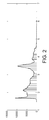
- FIG. 2 shows an example energy spectrum of high energy photon interactions in a scintillation detector in response to irradiating it with 511 keV photons and 1.2 MeV photons from a Na-22 source.
- FIG. 3 shows spatial distributions of high energy photon interactions in a position sensitive high energy photon scintillation crystal array detector.
- a high energy photon detector can record position (discrete or continuous) of high energy photon interactions.
- Embodiments of the invention provide, among other things, methods and systems for processing an analog signal that is generated by a high energy photon detector in response to a high energy photon interaction.
- a digital edge is generated representing the time of the interaction along a first path, and the energy of the interaction is encoded as a delay from the digital edge along a second path.
- the generated digital edge and the delay encode the time and energy of the analog signal using pulse width modulation.
- FIG. 1 shows arrival time difference spectra for a pair of coincident interactions of the two high energy (511 keV) photons generated from a positron-electron annihilation event
- FIG. 2 shows an example energy spectrum of high energy photon interactions in a scintillation detector in response to irradiating it with 511 keV photons and 1.2 MeV photons from a Na-22 source;
- FIG. 3 shows a 2-D histogram of spatial distributions of high energy photon interactions in a position-sensitive high energy photon scintillation crystal array detector
- FIG. 4 shows a PET block detector readout with light multiplexing
- FIG. 5 shows a detector with a multi-channel readout ASIC
- FIG. 6 shows a high channel count digital architecture with a front-end ASIC pulse width modulator, according to an embodiment of the present invention
- FIG. 7 shows an example front end circuit for a high energy photon detector, according to an embodiment of the present invention.
- FIG. 8 shows an example peak detector with delay circuit, according to an embodiment of the present invention.
- FIG. 9 shows an input scintillation signal entering a peak detector and a linear ramp discharge
- FIG. 10 shows example pulser linearity of a pulse width modulation circuit
- FIG. 11 shows a scope capture of an example pulse width modulation circuit including an input to a constant fraction discriminator, an output of a pulse width modulation (PWM), and a logic output of the PWM;
- PWM pulse width modulation
- FIG. 12 shows a correlation between example pulse width modulation and a standard analog-modulated processing chain
- FIG. 13 shows energy spectra of an ADC sampled pulse height of a standard analog-modulated processing chain and example pulse-width modulation for a LYSO-SSPM scintillation detector
- FIG. 14 shows an example pulse having a set rise and fall time
- FIG. 15 shows an embodiment of the present invention including a peak sense circuit
- FIG. 16 shows an embodiment of the present invention including a spatial information delay circuit
- FIG. 17 shows an embodiment of the present invention including a detector ID circuit.
- an event such as a scintillation event
- information from individual interactions is recorded, such as the time of the event, the energy of the event, and the location of the event.
- these parameters are determined through certain analog signal processing algorithms applied to the analog signals that the detector generates.
- the energy and location information may be processed using an analog-to-digital (ADC) converter that samples an analog value that is proportional to the integral of the charge created by the scintillation event.
- ADC analog-to-digital
- FIG. 4 shows light multiplexing being used to reduce the number of readout channels in a conventional PET block detector readout system 10 .
- a block detector 12 and photomultiplier tubes (PMT) 14 produces a signal sent over an analog bus to a low channel count (4-channel) ASIC 16 .
- PMT photomultiplier tubes
- ADCs 18 read each analog channel, the result of which is output to a readout system such as but not limited to a field programmable gate array (FGPA) 20 with suitable logic.
- FGPA field programmable gate array
- FIG. 5 shows a multi-channel readout system 22 including a multi-channel readout ASIC (32 or 64 channels) 24 combined with triggering, an analog memory, and a single ADC 26 , which reduces the number of channels 28 to a reasonable level.
- the high analog channel count ASIC 24 has problems with a high density analog bus 30 .
- pulse width modulation For an improved architecture to implement very high channel count PET data acquisition systems, pulse width modulation (PWM) has significant advantages over previous generations of readout architectures.
- embodiments of the present invention modulate the width, rather than the amplitude, of a digital pulse to be proportional to the integral of the charge created.
- the analog value of the outgoing digital pulses may be recovered by using a time-to-digital converter (TDC) in back-end electronics, preferably without the need for an ADC.
- TDC time-to-digital converter
- the same TDC used to record the time of the event can be used to recover the amplitude.
- embodiments of the invention provide methods, apparatuses, and systems for encoding photon interaction information, such as the arrival time, energy, and location of each high energy photon interaction in a detector using the different arrival times of various edges of a digital signal, rather than in the amplitude of an analog signal, as provided in conventional approaches.
- This pulse width modulation is analogous to the different methods of phase modulation and amplitude modulation of an analog carrier in continuous radio frequency modulation.
- Digital encoding of the signal especially onto a single wire or fiber, allows more flexibility and drastically simpler data acquisition electronics over analog encoding of the signal.
- an example circuit according to embodiments of the present invention allows a PWM readout scheme different from time over threshold PWM circuits used in high energy physics.
- PWM techniques simplify the routing to the back end electronics without degrading the performance of the system.
- An example readout architecture based on PWM processes digital rather than analog pulses, which can be very easily multiplexed, allowing one to achieve very high channel density required for ultra-high resolution, 3-D positioning high-energy photon detector systems.
- Apparatuses and systems according to certain embodiments of the invention include, but are not limited to, a front-end for an imaging system that couples to a high-energy photon detector, a front-end including a high-energy photon detector, and an imaging system having such front-ends.
- a nonlimiting example apparatus for performing methods according to the present invention is a front-end for a positron emission tomography (PET) system as shown in the following figures, though those of ordinary skill in the art will appreciate that other systems having emitted photons may be used.
- PET positron emission tomography
- PET is a medical imaging modality that uses positron emitting radionuclides attached to specific molecules that are introduced into the body of an animal and tracked by a PET system to provide sensitive assays of a wide range of biological processes relating to cancer or other diseases associated with alterations in the functional metabolism of cells in the body. Tracking is possible because the radionuclides emit high-energy photons that are detected with high spatial, spectral and temporal resolution by PET system detectors. For example, two high energy (e.g., 511 keV) photons are generated from a positron-electron annihilation event. The two photons interact in opposing high energy photon detectors (coincident interaction) aligned with the direction of photon emission.
- Embodiments of the present invention convert this exponentially decaying signal (e.g., via an exponentially decaying light signal or a signal from a direct bandgap semiconductor) into a digital edge and a width.
- time is encoded using a low jitter timing discriminator.
- the charge from the high energy interaction in the detector triggers a comparator.
- a logic signal is generated that is slightly delayed from the interaction.
- the energy of the signal is created by a circuit that converts the amplitude of the received charge into a time delay from the logic signal generated from the discriminator. This creates a pulse width, the width being the time difference between the first logic signal and the second, which is proportional to the amplitude.
- FIG. 6 shows a high channel count digital architecture 40 according to an embodiment of the present invention.
- Each of a plurality of detector channels 42 outputs via a digital bus 43 to a low channel count front-end ASIC pulse width modulator 44 , which in turn outputs to a high density digital bus 46 .
- no ADCs are needed to digitize amplitude modulation.
- This example system enables the move to a purely digital high density back end 48 embodied in suitable FPGA logic.
- Example methods and systems of the present invention encode the time, energy, and location of each high energy photon interaction in a detector using the different arrival times of various edges of a digital signal, rather than in the amplitude of an analog signal.
- An example PWM scheme marries the fast constant fraction discriminator (CFD) timing needed for PET and the time counter principles behind the Wilkinson ADC conversion technique for encoding amplitude. Because it is relatively simple to implement a very high degree of multiplexing using digital pulses, the example PWM readout architecture 40 can potentially readout more channels than a high density analog readout architecture without using ADCs.
- CFD fast constant fraction discriminator
- TOT time-over-threshold
- the noise of TOT depends on the shaping circuits used and strongly depends on the inherent non-linearity of the width versus amplitude dependence. Since the decay of a Gaussian-shaped pulse falls off exponentially with the time, it does not provide the good delay linearity needed for a robust PWM scheme.
- the data acquisition architectures of TOT are used in very high channel count physics experiments using silicon vertex trackers and calorimeters. New high resolution PET systems, as one example, have similar high channel count needs as these high energy physics experiments.
- an example high energy photon detection system such as but not limited to a PET system, includes a front end 50 having a high energy photon detector 52 that is positioned to detect photons from a source of emitted photons and produce an analog signal.
- the high energy photon detector 52 can include one of a plurality of high energy photon detectors, such as, but not limited to, one or more scintillation crystals coupled to one or more magnetically insensitive semiconductor photodetectors, one or more magnetically insensitive direct interaction semiconductors, or traditional photodetectors including photomultiplier tubes, etc.
- the high energy photon detector 52 produces an analog signal as a charge in response to a high energy photon interaction.
- This analog signal (e.g., charge) has a temporal dependence, and represents the energy of the incoming high energy photon.
- the signal varies in time based on the random process of radioactive decay and varies in energy based on the physical transport of photons through matter.
- the high energy photon detector 52 may be suitably coupled (e.g., electrically connected), directly or indirectly, to a pulse width modulation front-end circuit, including an analog preamplifier circuit, for example a shaping amplifier such as a charge sensitive preamplifier 54 .
- an analog preamplifier circuit for example a shaping amplifier such as a charge sensitive preamplifier 54 .
- a nonlimiting example of a charge sensitive preamplifier is based on an electrical circuit that produces a voltage that is proportional to charge.
- Example electrical couplings include discrete networks of components that pass the charge from the detector 52 to the preamplifier 54 .
- the charge sensitive preamplifier 54 converts the charge to a voltage signal output. For example, the preamplifier integrates the charge.
- the output is converted to a digital signal having a first edge (e.g., a rising edge) representing a time of the original analog signal, and second edge (e.g., a falling edge) representing amplitude.
- first edge e.g., a rising edge
- second edge e.g., a falling edge
- Each edge transition encodes a unique analog value.
- the time encoding and the energy encoding take place along two separate paths, which are referred to herein as a first path and a second path, though this designation is not intended to require a particular ordering.
- the output of the preamplifier circuit 54 (e.g., the integrated signal) is sent to a time encoding circuit, such as a timing discriminator 56 (e.g., constant fraction or leading edge), along a first path, generating a digital edge that represents the time of the start of the event.
- a timing discriminator 56 e.g., constant fraction or leading edge
- the timing discriminator 56 may, as a nonlimiting example, generate a digital edge at the time where the signal can be first reliably detected above noise.
- the time encoding circuit may, when a voltage or current of the analog signal crosses a threshold, generate a signal with the time of the event to provide a fixed edge.
- Timing discriminator is a constant fraction discriminator that generates a timing signal that is independent of the amplitude of the signal, though other time encoding circuits, such as but not limited to a good comparator, may also be used. It is preferred that the preamplifier circuit 54 and the timing discriminator 56 be combined into a single circuit (e.g., a single chip) suitably coupled to the high energy photon detector 52 .
- the output signal of the preamplifier circuit (e.g., the falling signal edge) is also connected to a delay encoding circuit along a second path that converts the width of the preamplifier circuit output signal to a delay from the first edge (produced by the timing discriminator).
- This splitting of the output signal into separate paths or channels for timing and energy encoding is significantly different from TOT methods, which conventionally have suffered from degraded timing and/or energy performance.
- a falling signal edge is produced with constant slope decay from a peak signal. Because the peak signal is proportional to the integral of the charge, and therefore the energy of the event, the amplitude will decay with a constant slope. By detecting when this amplitude decays to zero with a suitable detector such as a comparator, the delay from the start of the event is proportional to the amplitude.
- An example of a delay encoding circuit is a pulse width modulator.
- the pulse width modulator includes a peak detector circuit 58 that detects the peak after integrating and preferably shaping (e.g., Gaussian shaping or optimally filtering) the input charge. After detecting the peak, a detection circuit can enable a delay circuit 60 that is proportional to amplitude.
- An example of a delay circuit is a current source that discharges a capacitor. If the current is proportional to the amplitude, then the time to discharge the capacitor to no charge will be linearly related to the amplitude.
- the peak detector 58 records the peak of the integration, and the charge is converted to an amplitude over a certain time. The circuit detects when the peak has been reached, and begins discharging a timing element.
- a comparator detects when the amplitude of the delay circuit signal decays to zero or some other number. For example, the amplitude may be placed onto a capacitor.
- the preamplifier circuit immediately puts a rising edge on the output. Because the preamplifier integrates the input charge, the time from the start of the pulse to the peak is always a constant amount of time regardless of the amplitude of the pulse.
- the peak should be sampled after a fixed delay duration from the start of the pulse. That fixed delay time is application specific, and related to the time required for a given detector to reach the optimal signal-to-noise ratio. The peak can be reliably sampled by using a peak detection circuit.
- the amplitude then immediately starts a discharge from the capacitor in a controlled fashion (e.g., linear, though other methods may be used).
- a controlled fashion e.g., linear, though other methods may be used.
- the comparator indicates low.
- the low time minus the high time determines the width of the pulse.
- the delay from the start of the event is proportional to the amplitude, because the amplitude of the preamplifier circuit output decays with a constant slope. This signal represents the energy of the event.
- pulse width modulation circuit 50 one energy and one time value can be encoded into a single digital signal.
- the timing discriminator 56 is embodied in a constant fraction discriminator (CFD), which encodes the arrival time and reduces time walk. Additionally, the peak detector 58 captures the maximum signal from a Gaussian shaped signal and generates a ramp function that linearly decays to zero. By splitting the signal into two paths, the signal-to-noise-ratio (SNR) of coincidence timing can be optimized at the same time as the SNR of the energy signal.
- SNR signal-to-noise-ratio
- Certain TOT-based ASICs use little or no shaping to attain the best timing performance, and this severely degrades the SNR of the energy channel. Other TOT-based ASICs use Gaussian shaping with good SNR for energy performance, but this slow shaping significantly degrades timing performance.
- Another advantage of certain example embodiments of the present invention is that in certain types of high energy photon data acquisition, such as standard PET data acquisition, timing is performed by a constant fraction discriminator (CFD) to reduce the amplitude dependent time walk.
- CFD constant fraction discriminator
- the scintillation pulse is driven into a CFD that sets a latch 62 started at the rising edge.
- the scintillation signal may have some small amount of fast shaping to optimize the timing resolution.
- time pickoff an example design is identical to and will have the same performance as standard PET electronics.
- the pulse width modulation circuit 50 can be seen as an ADC operating on the energy portion of the scintillation pulse.
- the scintillation signal is first shaped by a Gaussian shaper (e.g., part of peak detector 58 ) set with a time constant to maximize SNR. Because the Gaussian shaper is a linear transform of the scintillation signal, the time between the start of the pulse and the peak of the Gaussian shaper will be constant. This is exploited in current PET detector readout electronics designs by firing a sample and hold to sample at this peak.
- an example embodiment implements a very fast peak detector with a linear ramp discharge.
- an example embodiment of the present invention provides a high speed analog peak detector 70 with RC delay circuit 72 .
- High speed Shockley diodes D 1 and D 2 are matched.
- An offset voltage of the Shockley diodes is needed due to the forward drop in the feedback of the op-amp.
- Capacitor C 1 holds the peak voltage.
- R 1 *C 1 The terminal of R 1 is tied to VEE to improve linearity.
- the resistors and capacitors can be changed to provide better dynamic range and less quantization noise with a corresponding tradeoff in pile-up at high event rates.
- a peak detector is simpler than the associated electronics to fire a sample-and-hold precisely at the peak of the signal.
- the example peak detector has a capacitor to store the value. With a simple resistor, an approximately linear discharge current can be generated that decays based on an RC product. The peak detector will begin to decay as soon as the output of the Gaussian shaper falls below the value of the storage capacitor.
- a sample-and-hold circuit would not have this limitation and could begin decaying immediately after sampling the value. Therefore, for an ASIC implementation, a sample-and-hold circuit would be preferred over a peak detector because the ramp could decay faster than the falling edge of the Gaussian shaper, which would improve count rate performance.
- the output of the PWM with a linear ramp discharge is fed into a high speed comparator with an adjustable threshold.
- the output of the comparator fires the reset of the latch 62 .
- the final digital signal has the rising edge encoding the arrival time of the scintillation pulse and the falling edge encoding the width of the pulse.
- ⁇ PWM 2 ⁇ CFD 2 + ⁇ COMP 2 + 2 ⁇ ⁇ ⁇ TDC 2 + ⁇ V CAP 2 + ⁇ V i 2 + ⁇ V t 2 ⁇ V / ⁇ t ( 1 )
- ⁇ v/ ⁇ t is the slope of the discharge
- ⁇ V i 2 is the variance of the peak input voltage signal
- ⁇ V t 2 is the variance of the comparator voltage threshold
- ⁇ V CAP 2 CAP is the variance of the voltage on the capacitor
- ⁇ CFD 2 is the variance of the CFD start timing
- ⁇ COMP 2 is the variance of the comparator stop timing
- ⁇ PWM 2 is the variance of the pulse width modulation timing
- ⁇ TDC 2 is the variance of quantization error of the time-to-digital converter
- max(V i ) is the maximum voltage of the input signal
- VEE is the negative supply
- RC is the resistor and capacitor used to select slope.
- the slope of the discharge is related to the value of the resistor R 1 and capacitor C 1 , as shown in FIG. 9 , and the negative supply voltage.
- an input scintillation signal indicated by a dark solid line, enters a peak detector with a linear ramp discharge, indicated by a light line.
- the upper dotted line represents the maximum of the signal and is proportional to maximum value of a Gaussian shaped signal.
- the lower dotted line represents the threshold for firing the trigger.
- the discharge is made more linear by connecting the terminal of the resistor to VEE.
- the slope is
- V / ⁇ t V i - VEE RC ⁇ VEE RC ⁇ ⁇ because ⁇ ⁇ V i ⁇ ⁇ ⁇ VEE ( 2 )
- the variance of the PWM can be converted into energy resolution by optimizing the voltage headroom of the circuits (max(V i ) ⁇ VEE/2, and max(V i ) ⁇ scaled so that it accommodates the 511 keV photopeak pulse height).
- the dead-time of this example PWM is different from ADC based converters. However, the dead-time of the example PWM is the same as that for a Wilkinson ADC, because the time to convert the amplitude is linearly related to the amplitude. For Wilkinson ADC or PWM circuits, the non-Poisson nature of the dead-time has been derived.
- the voltage noise terms of equation (3) should be made small relative to the input amplitude V i .
- the noise V cap is simply the kT/c noise of the storage capacitor. Usually, the noise of the front end detector is much larger than the noise of these simple elements.
- a key performance parameter to be optimized for certain embodiments of the present invention is the dynamic range versus the dead-time of the front-end detector.
- an example performance includes an 8-bit dynamic range for a pulse-width modulation (PWM) scheme, which is adequate for high resolution PET systems based on semiconductor detectors such as avalanche photodiodes (APD) or cadmium zinc telluride (CZT).
- PWM pulse-width modulation
- a discrete PWM test board was fabricated and evaluated for energy resolution performance versus a standard peak-sampled ADC.
- the example PWM circuit includes a peak detector with a linear ramp discharge and a high speed LT1171 comparator.
- the R was set at 10 k and the C at 100 pF, giving a slope of
- a 10 ⁇ Ci 22 Na source irradiated a 3 mm ⁇ 3 mm ⁇ 20 mm LYSO crystal connected to a single 3 mm ⁇ 3 mm solid state photomultiplier (SSPM) pixel of the SENSL 4 ⁇ 4 SPMArray 3035G16.
- the example test board contained a fast trans-impedance amplifier (500 Ohms) to amplify and invert the input signal for the input to an Ortec CFD-935.
- a CFD is very useful for the fast timing for an example PWM scheme.
- the output of the CFD was the start for the Ortec 567 TAC/SCA.
- the signal was shaped by a Cremat-200 100ns Gaussian shaping amplifier.
- the shaped signal was input to both the discrete PWM circuit and to an Ortec 427A delay amplifier.
- the latter channel enables comparison to the standard analog modulated processing chain.
- the PWM signal was sent to the stop of the Ortec 567 TAC/SCA.
- the output of the delay amplifier and the TAC went to an NI-1110 peak-sampling ADC.
- the Ortec 567 TAC/SCA is used to convert the pulse width back into an amplitude for digitization to mimic the function of the TDC and generate the PWM equivalent of a pulse height spectrum.
- the 22 Na energy spectrum was acquired fir both the standard analog-modulation, peak-sensing ADC chain and the PWM processing chain.
- FIG. 10 is a graph showing pulser linearity of the example PWM circuit.
- the linearity of the PWM circuit fits very closely to a second order polynomial over the dynamic range of the PWM. This second order behavior is solely determined by the discharge of the capacitor in the peak detector using a resistor with a large voltage offset.
- the example suffers from some non-linearity because the RC discharge is not a pure current source, this linearity is significantly improved over previous TOT designs and is sufficient for nearly all scintillation applications for PET.
- FIG. 11 shows a scope capture of the example PWM circuit with the input to the CFD (lower, gray), output of the PWM (upper, dark) and the logic output of the PWM that represents the integrated charge for each analog pulse (upper, light gray).
- the scope capture of the example PWM test board output pulses in FIG. 11 shows the working operation of the circuits for SSPM-based scintillation detection using 22 Na source irradiation.
- the dead-time for this circuit is approximately 600 ns for a 1.27 MeV photon pulse using a resistor of 10 k and a capacitor of 100 pF. For a 511 keV photon pulse, the dead-time would be approximately 400 ns.
- the dead-time for just the 100 ns Gaussian shaper is approximately 300 ns, or three times the shaping constant. Therefore, this example discrete PWM circuit implementation does not have a significant dead-time penalty.
- FIGS. 12 and 13 show PWM energy 22 Na energy spectra results, which correlate very well with the analog-modulated scheme.
- FIG. 13 shows the energy resolution of the two conversion schemes, which is identical at 19.4+/0.4% FWHM at 511 keV.
- the correlation between the ADC and PWM is 1.0 with a 1.2% standard deviation.
- This example PWM circuit is not fully able to linearize the low amplitude pulses from the 100 ns Gaussian shaper.
- An RC constant with a larger time constant relative to the shaper constant can be used to remove this small amplitude non-linearity, but this will increase dead-time. This small low-amplitude non-linearity should not be a significant detriment, however.
- Example PWM circuits provide a dynamic range, linearity, and SNR with a circuit that can in certain embodiments be relatively simple yet can meet performance parameters needed for high energy imaging, such as but not limited to PET data acquisition designs.
- Example PWM circuits and methods preserve the low jitter of CFD based triggering while deriving a pulse width from an optimally shaped signal, achieving a high SNR energy signal.
- Example circuits can perform well in high energy photon imaging applications, including but not limited to PET scintillation applications.
- Example circuits can be used to capture signals from, as nonlimiting examples, a light sharing block detector or a 3-D positioning sensitive detector because of the improved linearity and optimal SNR as compared to conventional, TOT designs for PET.
- both a constant rise time and fall time can be incorporated in the delay circuit to give a larger delay as a function of amplitude.
- An example of a high energy photon detection by a scintillation detection and analog front-end circuit with a constant rise and fall slope is shown in FIG. 14 .
- a peak sense 80 may be incorporated into a front-end circuit 82 to determine when the peak occurs.
- the peak sense 80 holds a peak value until being reset, providing a start delay.
- the signal from the peak sense 80 can also be compared to a constant delay circuit to determine which of the scintillator crystal types were hit, and this can be incorporated into the pulse signal.
- a high energy photon detector 52 may also provide spatial signals representing the spatial location of the high energy photon interaction within the detector. For example, as shown in the front end circuit 90 in FIG. 16 , the high energy photon detector 52 may output a signal, such as a spatially dependent charge ratio, which records the position (discrete or continuous) of the high energy photon interaction. The resulting output of the front end circuit 90 encodes time, energy, and location of a high energy photon interaction within the detector via a toggle 91 .
- such spatial signals of the detector can also be encoded using pulse width modulation, and these signals can create edges that are delayed from the edge that encodes the energy of the event.
- Examples of spatial information for four spatial channels e.g. channels a, b, c, and d, representing the x and y coordinates
- the peak sense 80 detector shown in FIG. 15 can also be useful for assisting processing of the spatial signals.
- a detector ID delay circuit 102 may output a detector ID in the form of binary code that uniquely identifies a detector.
- This detector ID may be encoded, for example, by binary encoding, or run-length encoding.
- the front-end circuit may include, for example, a circuit that combines the time, energy, spatial information, and one or more other signals (such as, but not limited to, a detector ID) into an output signal such as a pulse train.
- One or more output lines, but preferably one output line, from the front-end circuit may be a suitable output line for carrying the output signal.
- This output line may carry, for example electrical and/or optical signals, and thus may be an electrical and/or optical wire or wires.
- Optical coupling may be performed by a circuit that modulates the intensity of light in a laser diode.
- the light of the laser diode can be coupled into an optical fiber.
- the light of the laser can be detected using a photodetector.
- the light intensity can be converted into an electrical signal.
- the electrical signal can then be converted into a digital signal.
- Nonlimiting example embodiments for optical coupling are provided in U.S. patent application Ser. No. 12/246,326, filed Oct. 6, 2008, to the present inventors.
- the output signals for multiple detectors be multiplexed into as few output lines as possible. This is especially preferred if a signal detector has multiple signals.
- a position sensitive avalanche photodiode PSAPD
- a timing accurate comparator determines an arrival time of a first event.
- the 5 signals can be encoded (e.g., by a suitable logic circuit) such that the high-to-low transition of the first event leads to the second one, and onto the third, fourth, and fifth event. This cascaded modulation is especially useful for reducing the number of output lines needed (in this case, one wire transmits 5 encoded signals).
- Example readout systems include, but are not limited to, a time-to-digital converter, which converts the pulse width to an amplitude.
- Other suitable systems include a time-to-digital converter based on high speed counters.
- time-to-digital converters are already included in some known imaging devices, such as some known PET systems (for recording time information of a pulse). These may be used as a readout system, as would be appreciated by those of ordinary skill in the art.
- the decoded signal can then be processed according to methods known to those of ordinary skill in the art. Accordingly, example methods and systems of the present invention preferably are suitable for use with existing systems, such as imaging systems, as a front-end.
- a significant advantage of example embodiments of the present invention is a reduction in the number of electronic connections needed between the detector and the readout system. This advantage is provided because multi-parameter signals can be encoded into fewer wires or a single wire, rather than having several wires encoding the signal.
- High energy photon detection systems including but not limited to advanced positron emission tomography (PET) systems or other high energy photon/radionuclide detection systems, can have hundreds to many thousands of detectors. Each of these detectors must resolve the time, energy, and spatial information of a high energy photon interaction. In many imaging detectors, one signal encodes the digital trigger, which is used for timing information.
- the entire pulse duration should be minimized to allow for the highest number of detected pulses per unit time per signal wire.
- Filtering such as Gaussian shaping, can provide the largest signal-to-noise ratio for a given decay time constant for a scintillator while minimizing broadband noise. If an inadequate filtering time constant is chosen to minimize the pulse width, then a non-optimal signal-to-noise ratio will be achieved.
- a fixed, detector dependent, constant delay from the start of the signal to the peak of filtering circuit signal using the optimal time constant can be sampled in the peak detector.
- embodiments of the present invention provide the minimum pulse width for linear encoding of the output of a high energy photon detector.
- SNR signal-to-noise ratio
- analog multiplexing has no degradation in performance
- analog multiplexing reduces performance for each detector added into a multiplexing circuit.
- analog electronic multiplexing is a current method to attempt to reduce the number of readout channels. Detectors can be connected using spatial encoding so that many detectors can be read out using a common readout path. Analog electronic multiplexing, however, degrades the amplitude and timing information of the signal. Therefore, there is a limit to how many channels can be multiplexed together. As shown in FIG. 6 , digital signals, by contrast, can be almost infinitely multiplexed with very little degradation in performance. This allows for far fewer channels that digitize the signals without performance degradation.
- digital signals in example embodiments of the present invention can be transmitted by methods other than analog transmission.
- Examples of digital transmission include electronic transmission over a multiplex channel, or over an optical fiber.
- a digital output for example, may be coupled to a laser driver for generation of optical signals.
- the digital signal is much more robust in the present of noise, attenuation, and interference. As a nonlimiting example, it is easier to transmit digital signals using optical encoding over fiber using the same high performance telecommunications technology that is used to route digital packets.
- Analog signal transmission over wires is greatly constrained by noise and power requirements, whereas digital signal transmission over optical fibers has many advantages in applications that require relaying signals over great distance, in highly electromagnetically interfering environments, or both.
- the signals can be relayed over digital communication channels. This allows for a large reduction in the number of readout channels, and for robust delivery of the information signals to back end data processing electronics.
- PET detectors as part of a system according to embodiments of the present invention can be placed in environments where it has been difficult to operate, such as in an MR system.
- time-to-digital converters can be used to replace the analog-to-digital converters in embodiments of the present invention.
- the amplitude can be recovered using time-to-digital converters rather than analog to digital converters.
- Time-to-digital converters are already used in some conventional systems to recover the timing information of the pulse, and according to embodiments of the present invention they can be reused to give the amplitude and spatial information. This allows the elimination of analog-to-digital converters in a system if desired.
- Each of the hundreds to thousands of detectors in a conventional high energy photon/radionuclide detection system has sensitive analog circuits that must be connected over cables from the detector to devices or systems for data acquisition.
- Integrated circuits implementing pulse width modulation can be created directly in a detector simply and easily.
- the signals can be relayed over digital communication channels. This allows for a large reduction in the number of readout channels, and for robust delivery of the information signals to the back end data processing electronics.
- Example embodiments of the present invention can greatly reduce the cost of the data electronics, while at the same time allowing the placement of these detectors in harsh environments that hinder effective operation, such as but not limited to a magnetic resonance imaging (MRI) system.
- MRI magnetic resonance imaging
- Nonlimiting example applications for the present invention include high energy physics, such as scintillation or solid-state detectors, nuclear medicine applications, such as positron emission tomography (PET), gamma ray imaging, or single photon computed tomography (SPECT), defense applications for nuclear weapons proliferation or homeland defense, including gamma ray spectroscopy and imaging detection, and oil well drilling, such as by using scintillation detectors in harsh drilling environments.
- high energy physics such as scintillation or solid-state detectors
- nuclear medicine applications such as positron emission tomography (PET), gamma ray imaging, or single photon computed tomography (SPECT)
- PET positron emission tomography
- SPECT single photon computed tomography
- defense applications for nuclear weapons proliferation or homeland defense including gamma ray spectroscopy and imaging detection
- oil well drilling such as by using scintillation detectors in harsh drilling environments.
- PWM circuits are described, it will be appreciated by those of ordinary skill in the art that several modifications are possible.
- alternative linear ramp circuits could easily be implemented in ASICs or more discrete components to achieve much better linearity (though such circuits may increase complexity).
- the peak detector with resistive discharge can easily replaced by, for example, a sample-and-hold with current source discharge architecture in an ASIC design. This would remove the non-linearity for small signals that the peak-detection method may suffer from with small RC constants used to improve dead-time performance.
- the timing CFD of the front end may be replaced with a fast leading edge discriminator. The amplitude information may be used to remove the time walk.
- the same comparator that is used for timing not be used for the energy signal, otherwise a poor tradeoff between timing and energy SNR may result.
Abstract
Description
where ∂v/∂t is the slope of the discharge, σV
Linearity of the test board was tested by driving a pulser signal into the input preamplifier and measuring the output voltage after a TAC. For these tests, the TAC followed by an ADC mimics a TDC that may be used in an example PWM system.
Claims (24)
Priority Applications (1)
| Application Number | Priority Date | Filing Date | Title |
|---|---|---|---|
| US12/397,195 US8258480B2 (en) | 2008-03-03 | 2009-03-03 | High energy photon detection using pulse width modulation |
Applications Claiming Priority (2)
| Application Number | Priority Date | Filing Date | Title |
|---|---|---|---|
| US6790508P | 2008-03-03 | 2008-03-03 | |
| US12/397,195 US8258480B2 (en) | 2008-03-03 | 2009-03-03 | High energy photon detection using pulse width modulation |
Publications (2)
| Publication Number | Publication Date |
|---|---|
| US20100025589A1 US20100025589A1 (en) | 2010-02-04 |
| US8258480B2 true US8258480B2 (en) | 2012-09-04 |
Family
ID=41607370
Family Applications (1)
| Application Number | Title | Priority Date | Filing Date |
|---|---|---|---|
| US12/397,195 Active 2030-04-01 US8258480B2 (en) | 2008-03-03 | 2009-03-03 | High energy photon detection using pulse width modulation |
Country Status (1)
| Country | Link |
|---|---|
| US (1) | US8258480B2 (en) |
Cited By (9)
| Publication number | Priority date | Publication date | Assignee | Title |
|---|---|---|---|---|
| CN103412319A (en) * | 2013-08-19 | 2013-11-27 | 中国科学院高能物理研究所 | Detector signal processing method and device based on pulse width spectrum |
| US8774356B2 (en) * | 2011-05-20 | 2014-07-08 | Rigaku Corporation | Wavelength dispersive X-ray fluorescence spectrometer |
| CN105425270A (en) * | 2014-05-28 | 2016-03-23 | 上海联影医疗科技有限公司 | Positron emission tomography (PET) detector, method for setting PET detector and detecting method thereof |
| US20170035376A1 (en) * | 2015-08-06 | 2017-02-09 | Texas Instruments Incorporated | Low power photon counting system |
| US9606245B1 (en) | 2015-03-24 | 2017-03-28 | The Research Foundation For The State University Of New York | Autonomous gamma, X-ray, and particle detector |
| US10151845B1 (en) | 2017-08-02 | 2018-12-11 | Texas Instruments Incorporated | Configurable analog-to-digital converter and processing for photon counting |
| US20190033471A1 (en) * | 2017-07-28 | 2019-01-31 | Shenzhen United Imaging Healthcare Co., Ltd. | Positron emission tomography detecting device |
| US10877169B2 (en) | 2015-08-10 | 2020-12-29 | Shanghai United Imaging Healthcare Co., Ltd. | Apparatus and method for pet detector |
| US10890674B2 (en) | 2019-01-15 | 2021-01-12 | Texas Instruments Incorporated | Dynamic noise shaping in a photon counting system |
Families Citing this family (26)
| Publication number | Priority date | Publication date | Assignee | Title |
|---|---|---|---|---|
| US8729486B2 (en) | 2010-06-23 | 2014-05-20 | The Board Of Trustees Of The Leland Stanford Junior University | MODFET active pixel X-ray detector |
| US9129220B2 (en) | 2010-07-07 | 2015-09-08 | Qualcomm Incorporated | Methods and systems for digital neural processing with discrete-level synapes and probabilistic STDP |
| CN102565845B (en) * | 2010-12-31 | 2013-11-06 | 同方威视技术股份有限公司 | Gamma ray spectrometry radionuclide identification method utilizing multiple detectors |
| US9006664B2 (en) * | 2011-02-23 | 2015-04-14 | Siemens Medical Solutions Usa, Inc. | Encoding for nuclear medical imaging block detectors |
| CN102338880B (en) * | 2011-06-02 | 2012-12-26 | 中国科学技术大学 | Nuclear pulse amplitude digitizing method and system |
| US11313678B2 (en) | 2011-06-30 | 2022-04-26 | The Regents Of The University Of Colorado | Remote measurement of shallow depths in semi-transparent media |
| US10684362B2 (en) | 2011-06-30 | 2020-06-16 | The Regents Of The University Of Colorado | Remote measurement of shallow depths in semi-transparent media |
| DK2705350T3 (en) | 2011-06-30 | 2017-06-19 | Univ Colorado Regents | REMOVE LOW DEPTH IN SEMI-TRANSPARENT MEDIA |
| US11231502B2 (en) | 2011-06-30 | 2022-01-25 | The Regents Of The University Of Colorado | Remote measurement of shallow depths in semi-transparent media |
| US11933899B2 (en) | 2011-06-30 | 2024-03-19 | The Regents Of The University Of Colorado | Remote measurement of shallow depths in semi-transparent media |
| EP2629118A3 (en) * | 2012-02-15 | 2017-09-06 | CSEM Centre Suisse d'Electronique et de Microtechnique SA - Recherche et Développement | High-sensitivity x-ray detector |
| CN104639123B (en) | 2013-11-14 | 2017-08-25 | 苏州瑞派宁科技有限公司 | The time point acquisition methods and device of threshold value are crossed in scintillation pulse |
| KR101647395B1 (en) | 2015-04-10 | 2016-08-10 | 서강대학교산학협력단 | Radiation apparatus and radiation detection signal processing method using bipolar time-over-threshold method |
| CN105064988A (en) * | 2015-08-04 | 2015-11-18 | 中国科学院声学研究所 | Slim-hole natural gamma spectrometry logging device |
| US9778383B2 (en) * | 2015-09-16 | 2017-10-03 | Siemens Medical Solutions Usa, Inc. | Transmission of PET-signals by means of time division multiplexing |
| KR102057198B1 (en) | 2016-02-22 | 2019-12-18 | 삼성전자주식회사 | Method and apparatus for storing x-ray data to at least one x-ray detection module |
| CN107797133A (en) * | 2016-08-31 | 2018-03-13 | 同方威视技术股份有限公司 | Multipotency area signal processing apparatus and multipotency area radiation detecting system and method |
| FR3058230B1 (en) * | 2016-10-27 | 2019-03-15 | Detection Technology Sas | SPECTROMETRY DEVICE |
| KR101815290B1 (en) * | 2016-11-14 | 2018-01-11 | 서강대학교산학협력단 | Multiplexing signal processing method using bipolar pulse |
| FR3063410B1 (en) * | 2017-02-28 | 2021-04-30 | Inst Mines Telecom | ANALOGUE ACQUISITION CIRCUIT FOR SIGNALS FROM RADIATIONS AND APPARATUS FOR PRODUCING AN IMAGE REPRESENTATIVE OF THESE RADIATIONS |
| US10575800B2 (en) * | 2017-03-08 | 2020-03-03 | Prismatic Sensors Ab | Increased spatial resolution for photon-counting edge-on x-ray detectors |
| EP3385756A1 (en) * | 2017-04-06 | 2018-10-10 | Koninklijke Philips N.V. | Pulse shaper |
| EP3434187A1 (en) | 2017-07-27 | 2019-01-30 | Koninklijke Philips N.V. | Motion compensated cardiac valve reconstruction |
| CN107450092B (en) * | 2017-08-23 | 2019-07-26 | 中派科技(深圳)有限责任公司 | For measuring the device of photon information |
| CN112946723B (en) * | 2021-02-05 | 2022-10-25 | 明峰医疗系统股份有限公司 | Method and system for energy measurement and position measurement of PET detector |
| CN116320329B (en) * | 2023-05-10 | 2023-09-15 | 深圳芯迈微科技有限公司 | Integrated chip of optical fiber access terminal system |
Citations (7)
| Publication number | Priority date | Publication date | Assignee | Title |
|---|---|---|---|---|
| US6114703A (en) | 1997-10-21 | 2000-09-05 | The Regents Of The University Of California | High resolution scintillation detector with semiconductor readout |
| US20040124360A1 (en) | 2002-09-18 | 2004-07-01 | The Regents Of The University Of California | Scintillation crystal detection arrays for radiation imaging devices |
| US20070102641A1 (en) | 2004-12-29 | 2007-05-10 | Schmand Matthias J | Combined PET/MR Imaging System and APD-Based PET Detector For Use In Simultaneous PET/MR Imaging |
| US20080042070A1 (en) | 2004-09-30 | 2008-02-21 | Levin Craig S | Semiconductor Crystal High Resolution Imager |
| WO2008040384A1 (en) | 2006-10-04 | 2008-04-10 | Cern - European Organization For Nuclear Research | Readout circuit for use in a combined pet-ct apparatus |
| US20080203309A1 (en) * | 2005-04-22 | 2008-08-28 | Koninklijke Philips Electronics N.V. | Digital silicon photomultiplier for TOF-PET |
| US20090093710A1 (en) | 2007-10-04 | 2009-04-09 | Levin Craig S | Optically coupled readout front-end for imaging system |
-
2009
- 2009-03-03 US US12/397,195 patent/US8258480B2/en active Active
Patent Citations (9)
| Publication number | Priority date | Publication date | Assignee | Title |
|---|---|---|---|---|
| US6114703A (en) | 1997-10-21 | 2000-09-05 | The Regents Of The University Of California | High resolution scintillation detector with semiconductor readout |
| US20040124360A1 (en) | 2002-09-18 | 2004-07-01 | The Regents Of The University Of California | Scintillation crystal detection arrays for radiation imaging devices |
| US7049600B2 (en) | 2002-09-18 | 2006-05-23 | The Board Of Trustees Of The Leland Stanford Junior University | Scintillation crystal detection arrays for radiation imaging devices |
| US20080042070A1 (en) | 2004-09-30 | 2008-02-21 | Levin Craig S | Semiconductor Crystal High Resolution Imager |
| US20070102641A1 (en) | 2004-12-29 | 2007-05-10 | Schmand Matthias J | Combined PET/MR Imaging System and APD-Based PET Detector For Use In Simultaneous PET/MR Imaging |
| US20080203309A1 (en) * | 2005-04-22 | 2008-08-28 | Koninklijke Philips Electronics N.V. | Digital silicon photomultiplier for TOF-PET |
| WO2008040384A1 (en) | 2006-10-04 | 2008-04-10 | Cern - European Organization For Nuclear Research | Readout circuit for use in a combined pet-ct apparatus |
| US20100078569A1 (en) * | 2006-10-04 | 2010-04-01 | Cern - European Organization For Nuclear Research | Apparatus and method for medical imaging |
| US20090093710A1 (en) | 2007-10-04 | 2009-04-09 | Levin Craig S | Optically coupled readout front-end for imaging system |
Non-Patent Citations (16)
| Title |
|---|
| Albuquerque, E., et al., "The Clear-PEM Electronics System," IEEE Transactions on Nuclear Science, vol. 53, No. 5, pp. 2704-2711, Oct. 2006. |
| Anghinolfi, F., et al., "NINO: An ultrafast low-power front-end amplifier discriminator for the time-of-flight detector in the ALICE experiment," IEEE Trans. Nucl. Sci. 51, 1974 (2004). |
| Catana, C., et al., "Simultaneous acquisition of multislice PET and MR images: initial results with a MR-compatible PET scanner," J Nucl Med. Dec. 2006;47(12):1968:76. |
| Fries, M.D., et al., "High-precision TDC in an FPGA using a 192 MHz quadrature clock," Nuclear Science Symposium Conference Record, 2002 IEEE, vol. 1, No., pp. 580-584, vol. 1, Nov. 10-16, 2002. |
| Jinyuan, et al., "Firmware-only Implementation of Time-to-Digital Converter (TDC) in Field-Programmable Gate Array (FPGA)," Nuclear Science Symposium Conference Record, 2003 IEEE, vol. 1, pp. 177-181, Oct. 2003. |
| Kephart, R., et al., "E-537 MWPC amplifier", FNAL; ERA-10-009019; EDB-85-024438, 1979. |
| Kipnis, I., et al., "A time-over-threshold machine: the readout integrated circuit for the BABAR Silicon Vertex Tracker," Nuclear Science, IEEE Transactions on , vol. 44, No. 3, pp. 289-297, Jun. 1997. |
| Krieger, B., et al., "SVX4: a new deep-submicron readout IC for the Tevatron collider at Fermilab," Nuclear Science, IEEE Transactions on , vol. 51, No. 5, pp. 1968-1973, Oct. 2004. |
| Levin, C.S., et al., "Investigation of position sensitive avalanche photodiodes for a new high-resolution PET detector design," Nuclear Science, IEEE Transactions on , vol. 51, No. 3, pp. 805-810, Jun. 2004. |
| Manfredi, P. F., et al., "Noise limits in a front-end system based on time-over-threshold signal processing, Nuclear Instruments and Methods in Physics Research Section A: Accelerators, Spectrometers, Detectors and Associated Equipment," vol. 439, Issues 2-3, Jan. 11, 2000, pp. 361-367. |
| Meyer, T.C., et al., "A Time-Based Front End Readout System for PET & CT," Nuclear Science Symposium Conference Record, 2006. IEEE, vol. 4, no., pp. 2494-2498, Oct. 29-Nov. 1, 2006. |
| Olcott and Levin, "Pulse Width Modulation: a Novel Readout Scheme for High Energy Photon Detection", 2008, IEEE Nuclear Symposium Conference Record, pp. 4530-4530. |
| Paneque et al., "Analogue Signal Transmission by an Optical Fiber System for the Camera of the MAGIC Telescope", 28th Intl. Cosmic Ray Conference, 2003, pp. 2927-2930. |
| Pichler, B.J., et al., "Performance test of an LSO-APD detector in a 7-T MRI scanner for simultaneous PET/MRI," J. Nucl Med. Apr. 2006;47(4):639-47. |
| Pratte, J.F., et al., "The RatCAP Front-End ASIC," IEEE Transactions on Nuclear Science, vol. 55, No. 5, pp. 2727-2735, Oct. 2008. |
| Shimazoe, K., et al., "Novel front-end pulse processing scheme for PET system based on pulse width modulation and pulse train method," Nuclear Science Symposium Conference Record, 2007. NSS '07. IEEE, vol. 6, no., pp. 4612-4614, Oct. 26-Nov. 3, 2007. |
Cited By (17)
| Publication number | Priority date | Publication date | Assignee | Title |
|---|---|---|---|---|
| US8774356B2 (en) * | 2011-05-20 | 2014-07-08 | Rigaku Corporation | Wavelength dispersive X-ray fluorescence spectrometer |
| CN103412319A (en) * | 2013-08-19 | 2013-11-27 | 中国科学院高能物理研究所 | Detector signal processing method and device based on pulse width spectrum |
| CN105425270A (en) * | 2014-05-28 | 2016-03-23 | 上海联影医疗科技有限公司 | Positron emission tomography (PET) detector, method for setting PET detector and detecting method thereof |
| US9606245B1 (en) | 2015-03-24 | 2017-03-28 | The Research Foundation For The State University Of New York | Autonomous gamma, X-ray, and particle detector |
| US9835737B1 (en) | 2015-03-24 | 2017-12-05 | The Research Foundation For The State University Of New York | Autonomous gamma, X-ray, and particle detector |
| US20170035376A1 (en) * | 2015-08-06 | 2017-02-09 | Texas Instruments Incorporated | Low power photon counting system |
| US10098595B2 (en) * | 2015-08-06 | 2018-10-16 | Texas Instruments Incorporated | Low power photon counting system |
| US10877169B2 (en) | 2015-08-10 | 2020-12-29 | Shanghai United Imaging Healthcare Co., Ltd. | Apparatus and method for pet detector |
| US11782175B2 (en) | 2015-08-10 | 2023-10-10 | Shanghai United Imaging Healthcare Co., Ltd. | Apparatus and method for PET detector |
| US11378702B2 (en) | 2015-08-10 | 2022-07-05 | Shanghai United Imaging Healthcare Co., Ltd. | Apparatus and method for PET detector |
| US20190033471A1 (en) * | 2017-07-28 | 2019-01-31 | Shenzhen United Imaging Healthcare Co., Ltd. | Positron emission tomography detecting device |
| US10768315B2 (en) * | 2017-07-28 | 2020-09-08 | Shanghai United Imaging Healthcare Co., Ltd. | Positron emission tomography detecting device |
| US11822025B2 (en) | 2017-07-28 | 2023-11-21 | Shanghai United Imaging Healthcare Co., Ltd. | Positron emission tomography detecting device |
| US10481283B2 (en) | 2017-08-02 | 2019-11-19 | Texas Instruments Incorporated | Configurable analog-to-digital converter and processing for photon counting |
| US10151845B1 (en) | 2017-08-02 | 2018-12-11 | Texas Instruments Incorporated | Configurable analog-to-digital converter and processing for photon counting |
| US10890674B2 (en) | 2019-01-15 | 2021-01-12 | Texas Instruments Incorporated | Dynamic noise shaping in a photon counting system |
| US11493649B2 (en) | 2019-01-15 | 2022-11-08 | Texas Instruments Incorporated | Dynamic noise shaping in a photon counting system |
Also Published As
| Publication number | Publication date |
|---|---|
| US20100025589A1 (en) | 2010-02-04 |
Similar Documents
| Publication | Publication Date | Title |
|---|---|---|
| US8258480B2 (en) | High energy photon detection using pulse width modulation | |
| EP2257835B1 (en) | Single photon radiation detector | |
| US7709801B2 (en) | Nuclear medicine diagnosis equipment | |
| Spanoudaki et al. | Use of single photon counting detector arrays in combined PET/MR: Characterization of LYSO-SiPM detector modules and comparison with a LSO-APD detector | |
| Nadig et al. | Evaluation of the PETsys TOFPET2 ASIC in multi-channel coincidence experiments | |
| KR20160067848A (en) | Image-capturing device, radiation detection apparatus, and control method for image-capturing device | |
| Bugalho et al. | Experimental characterization of the TOFPET2 ASIC | |
| US8076646B2 (en) | Burst-mode readout for solid state radiation detectors using partitioned pipeline architecture | |
| CN113167916A (en) | Radiation detection device with reflector | |
| US7737404B2 (en) | Signal acquisition in PET scanners | |
| CN111896991A (en) | Radiation imaging detection method and device | |
| US9006664B2 (en) | Encoding for nuclear medical imaging block detectors | |
| Olcott et al. | Pulse width modulation: A novel readout scheme for high energy photon detection | |
| JP2022095735A (en) | Radiation detection apparatus having analyzer within housing | |
| Meyer et al. | A time-based front end readout system for PET & CT | |
| US6977380B2 (en) | Low noise, long integration time acquisition for radiation detectors | |
| US10760960B2 (en) | Coincidence resolving time readout circuit | |
| Perri et al. | Amplitude Measurements with SiPM and ASIC (Citiroc 1A) Front-End Electronics | |
| Stapels et al. | Solid-state photomultiplier in CMOS technology for gamma-ray detection and imaging applications | |
| Johnson et al. | Energy resolution in CMOS SSPM detectors coupled to an LYSO scintillator | |
| Streun et al. | A compact PET detector readout using charge-to-time conversion | |
| Habte et al. | Study of low noise multichannel readout electronics for high sensitivity PET systems based on avalanche photodiode arrays | |
| Liu et al. | Ultra-Low Level Light Detection Based on the Poisson Statistics Algorithm and a Double Time Windows Technique With Silicon Photomultiplier | |
| Cho et al. | A design of a valid signal selecting and position decoding ASIC for PET using silicon photomultipliers | |
| Boxer et al. | Studies in pulse shape discrimination for an optimized ASIC design |
Legal Events
| Date | Code | Title | Description |
|---|---|---|---|
| AS | Assignment |
Owner name: NATIONAL INSTITUTES OF HEALTH (NIH), U.S. DEPT. OF Free format text: EXECUTIVE ORDER 9424, CONFIRMATORY LICENSE;ASSIGNOR:STANFORD UNIVERSITY;REEL/FRAME:022396/0400 Effective date: 20090312 |
|
| AS | Assignment |
Owner name: THE BOARD OF TRUSTEES OF THE LELAND STANFORD JUNIO Free format text: ASSIGNMENT OF ASSIGNORS INTEREST;ASSIGNORS:OLCOTT, PETER D.;LEVIN, CRAIG S.;SIGNING DATES FROM 20091012 TO 20091013;REEL/FRAME:023391/0382 |
|
| STCF | Information on status: patent grant |
Free format text: PATENTED CASE |
|
| CC | Certificate of correction | ||
| FEPP | Fee payment procedure |
Free format text: PAT HOLDER NO LONGER CLAIMS SMALL ENTITY STATUS, ENTITY STATUS SET TO UNDISCOUNTED (ORIGINAL EVENT CODE: STOL); ENTITY STATUS OF PATENT OWNER: LARGE ENTITY |
|
| FPAY | Fee payment |
Year of fee payment: 4 |
|
| FEPP | Fee payment procedure |
Free format text: MAINTENANCE FEE REMINDER MAILED (ORIGINAL EVENT CODE: REM.); ENTITY STATUS OF PATENT OWNER: LARGE ENTITY |
|
| FEPP | Fee payment procedure |
Free format text: 7.5 YR SURCHARGE - LATE PMT W/IN 6 MO, LARGE ENTITY (ORIGINAL EVENT CODE: M1555); ENTITY STATUS OF PATENT OWNER: LARGE ENTITY |
|
| MAFP | Maintenance fee payment |
Free format text: PAYMENT OF MAINTENANCE FEE, 8TH YEAR, LARGE ENTITY (ORIGINAL EVENT CODE: M1552); ENTITY STATUS OF PATENT OWNER: LARGE ENTITY Year of fee payment: 8 |
|
| MAFP | Maintenance fee payment |
Free format text: PAYMENT OF MAINTENANCE FEE, 12TH YEAR, LARGE ENTITY (ORIGINAL EVENT CODE: M1553); ENTITY STATUS OF PATENT OWNER: LARGE ENTITY Year of fee payment: 12 |