US8207940B2 - Wireless optical input device - Google Patents
Wireless optical input device Download PDFInfo
- Publication number
- US8207940B2 US8207940B2 US12/179,490 US17949008A US8207940B2 US 8207940 B2 US8207940 B2 US 8207940B2 US 17949008 A US17949008 A US 17949008A US 8207940 B2 US8207940 B2 US 8207940B2
- Authority
- US
- United States
- Prior art keywords
- mode
- activity
- power
- data
- image data
- Prior art date
- Legal status (The legal status is an assumption and is not a legal conclusion. Google has not performed a legal analysis and makes no representation as to the accuracy of the status listed.)
- Expired - Lifetime, expires
Links
- 230000003287 optical effect Effects 0.000 title claims abstract description 125
- 230000000694 effects Effects 0.000 claims abstract description 122
- 230000033001 locomotion Effects 0.000 claims abstract description 78
- 238000000034 method Methods 0.000 claims abstract description 18
- 238000012545 processing Methods 0.000 claims description 16
- 239000013598 vector Substances 0.000 claims description 9
- 238000004590 computer program Methods 0.000 claims 2
- 238000006073 displacement reaction Methods 0.000 claims 1
- 230000002028 premature Effects 0.000 abstract description 3
- 241000699666 Mus <mouse, genus> Species 0.000 description 49
- 230000007704 transition Effects 0.000 description 48
- 238000005516 engineering process Methods 0.000 description 17
- 230000004044 response Effects 0.000 description 14
- 238000012797 qualification Methods 0.000 description 12
- 238000004458 analytical method Methods 0.000 description 10
- 230000000875 corresponding effect Effects 0.000 description 10
- 230000009471 action Effects 0.000 description 8
- 230000006854 communication Effects 0.000 description 8
- 238000004891 communication Methods 0.000 description 8
- 238000010586 diagram Methods 0.000 description 8
- 210000003811 finger Anatomy 0.000 description 6
- 230000000712 assembly Effects 0.000 description 5
- 238000000429 assembly Methods 0.000 description 5
- 230000008901 benefit Effects 0.000 description 5
- 238000013519 translation Methods 0.000 description 5
- 230000008859 change Effects 0.000 description 4
- 230000006870 function Effects 0.000 description 4
- 238000007619 statistical method Methods 0.000 description 4
- 230000002459 sustained effect Effects 0.000 description 4
- 241000282326 Felis catus Species 0.000 description 3
- 241000699670 Mus sp. Species 0.000 description 3
- 230000005540 biological transmission Effects 0.000 description 3
- 230000001276 controlling effect Effects 0.000 description 3
- 230000008842 detection of inactivity Effects 0.000 description 3
- 229910044991 metal oxide Inorganic materials 0.000 description 3
- 150000004706 metal oxides Chemical class 0.000 description 3
- 239000004065 semiconductor Substances 0.000 description 3
- 230000011664 signaling Effects 0.000 description 3
- 239000000872 buffer Substances 0.000 description 2
- 230000000295 complement effect Effects 0.000 description 2
- 210000000245 forearm Anatomy 0.000 description 2
- 238000010191 image analysis Methods 0.000 description 2
- 230000035484 reaction time Effects 0.000 description 2
- 230000000284 resting effect Effects 0.000 description 2
- 238000005096 rolling process Methods 0.000 description 2
- 230000035945 sensitivity Effects 0.000 description 2
- 210000003813 thumb Anatomy 0.000 description 2
- 230000001960 triggered effect Effects 0.000 description 2
- WHXSMMKQMYFTQS-UHFFFAOYSA-N Lithium Chemical compound [Li] WHXSMMKQMYFTQS-UHFFFAOYSA-N 0.000 description 1
- HBBGRARXTFLTSG-UHFFFAOYSA-N Lithium ion Chemical compound [Li+] HBBGRARXTFLTSG-UHFFFAOYSA-N 0.000 description 1
- PXHVJJICTQNCMI-UHFFFAOYSA-N Nickel Chemical compound [Ni] PXHVJJICTQNCMI-UHFFFAOYSA-N 0.000 description 1
- HCHKCACWOHOZIP-UHFFFAOYSA-N Zinc Chemical compound [Zn] HCHKCACWOHOZIP-UHFFFAOYSA-N 0.000 description 1
- 238000013459 approach Methods 0.000 description 1
- 230000007175 bidirectional communication Effects 0.000 description 1
- OJIJEKBXJYRIBZ-UHFFFAOYSA-N cadmium nickel Chemical compound [Ni].[Cd] OJIJEKBXJYRIBZ-UHFFFAOYSA-N 0.000 description 1
- 239000003990 capacitor Substances 0.000 description 1
- 238000003708 edge detection Methods 0.000 description 1
- 230000005684 electric field Effects 0.000 description 1
- 210000002683 foot Anatomy 0.000 description 1
- 238000005305 interferometry Methods 0.000 description 1
- 229910052744 lithium Inorganic materials 0.000 description 1
- 229910001416 lithium ion Inorganic materials 0.000 description 1
- 230000007257 malfunction Effects 0.000 description 1
- 238000010338 mechanical breakdown Methods 0.000 description 1
- 230000007246 mechanism Effects 0.000 description 1
- 238000012986 modification Methods 0.000 description 1
- 230000004048 modification Effects 0.000 description 1
- 238000012544 monitoring process Methods 0.000 description 1
- 229910000652 nickel hydride Inorganic materials 0.000 description 1
- 230000002093 peripheral effect Effects 0.000 description 1
- 229920000642 polymer Polymers 0.000 description 1
- 230000008569 process Effects 0.000 description 1
- 230000001105 regulatory effect Effects 0.000 description 1
- 230000017280 response to inactivity Effects 0.000 description 1
- 238000012163 sequencing technique Methods 0.000 description 1
- 230000002618 waking effect Effects 0.000 description 1
- 229910052725 zinc Inorganic materials 0.000 description 1
- 239000011701 zinc Substances 0.000 description 1
Images


Classifications
-
- G—PHYSICS
- G06—COMPUTING; CALCULATING OR COUNTING
- G06F—ELECTRIC DIGITAL DATA PROCESSING
- G06F3/00—Input arrangements for transferring data to be processed into a form capable of being handled by the computer; Output arrangements for transferring data from processing unit to output unit, e.g. interface arrangements
- G06F3/01—Input arrangements or combined input and output arrangements for interaction between user and computer
- G06F3/03—Arrangements for converting the position or the displacement of a member into a coded form
- G06F3/0304—Detection arrangements using opto-electronic means
- G06F3/0317—Detection arrangements using opto-electronic means in co-operation with a patterned surface, e.g. absolute position or relative movement detection for an optical mouse or pen positioned with respect to a coded surface
Landscapes
- Engineering & Computer Science (AREA)
- General Engineering & Computer Science (AREA)
- Theoretical Computer Science (AREA)
- Human Computer Interaction (AREA)
- Physics & Mathematics (AREA)
- General Physics & Mathematics (AREA)
- Position Input By Displaying (AREA)
Abstract
One embodiment of the present invention provides a wireless input device that employs optical sensing to effect the likes of cursor movement and scrolling. Power management techniques can be optionally employed to avoid premature depletion of the wireless input device's power source. Another embodiment of the present invention provides a wireless device having a power management algorithm controlling its power consumption. Another embodiment of the present invention provides a method for managing the power consumption of a wireless device.
Description
This application is a continuation of U.S. patent application Ser. No. 10/809,626, filed Mar. 24, 2004, entitled “Wireless Optical Input Device”, which is a continuation of U.S. patent application Ser. No. 09/709,046, filed Nov. 9, 2000, entitled “Wireless Optical Input Device”, the contents of each of which are incorporated by reference.
1. Field of the Invention
The invention relates to wireless devices, and more particularly, to a wireless optical input device that allows a user to interact with a computer.
2. Description of the Background
There are a number of computer input devices that employ an electromechanical arrangement for effecting cursor movement and scrolling. In such an arrangement, the mechanical movement of a roller ball is converted into electrical signals. The electrical signals are then encoded into information that a computer can use, such as cursor X-Y position data or scrolling direction and distance. Mice and trackballs are the most common input devices that employ this type of electromechanical arrangement. In general, however, there are numerous applications for an electromechanical arrangement in computer input devices.
One problem associated with this type of electromechanical arrangement is that the actuating assembly (e.g., roller ball and the corresponding rollers) is prone to malfunction because of debris and or mechanical breakdown. Moreover, input devices such as mice require that the roller ball be in contact with a special surface (e.g., mouse pad) in order to function properly. This special surface is equally prone to debris and wear and tear, and tends to limit the area upon which the input device can move. For example, at times, a user may have to stop rolling the mouse, pick it up, and place it back down on the mouse pad so that the user can keep moving the mouse in the same direction in order to get the cursor to a desired position.
In response to solving these problems, optical assemblies have begun to replace the electromechanical assemblies. Unlike its electromechanical counterpart, an optical assembly does not have a roller ball and the corresponding rollers. As such, an input device employing an optical sensor assembly for performing functions such as cursor movement and scrolling is not prone to debris or mechanical wear, and can be used on most surfaces. Generally, an optical sensor assembly employs an optical sensor and a light emitting diode (LED). As the input device is moved, light from the LED reflects off a surface and is received by the optical sensor thereby forming a series of images. Distance and direction of cursor or scroll bar movement can then be determined from the images. In short, optical input devices provide an elegant solution to problems associated with electromechanical input devices.
However, it appears that there is currently no computer input device that employs such optical sensing technology in the context of a wireless input device. Wireless technology allows input devices such as mice and keyboards to be untethered from the host computer thereby providing the user with a greater degree of mobility and reducing desktop clutter. Thus, there is a need for an input device that offers the benefits of a wireless connection as well as the benefits associated with an optical sensor for effecting cursor movement, such as a wireless optical mouse.
Problems associated with such a wireless optical input device stem from competing factors underlying the two technologies. For instance, on one hand, optical assemblies require a significant amount of power (e.g., for powering the LED and optical sensor). On the other hand, wireless input devices are not tethered to an external power source. Thus, one must be provided internally to such a wireless input device. This basically limits the power source to a battery included in the wireless input device. To complicate matters, both practical and economic reasons dictate that the battery size cannot exceed certain physical constraints thereby limiting the life of the battery. As such, power intensive technology can prematurely deplete a battery included in a wireless input device. Hence, an effective power management scheme should be available to such a device.
There is a need, therefore, for a wireless input device that employs optical sensing to effect the likes of cursor movement and scrolling. Such a wireless input device should optionally employ power management techniques that allow the battery to avoid premature depletion. In a more general sense, there is a need for power management techniques in wireless devices that employ power intensive technology.
One embodiment of the present invention provides a wireless input device that employs optical sensing to effect the likes of cursor movement and scrolling. The wireless input device can optionally employ power management techniques that allow the wireless input device's power source to avoid premature depletion. Another embodiment of the present invention provides a wireless device having a power management algorithm controlling its power consumption. Another embodiment of the present invention provides a method for managing the power consumption of a wireless device.
The features and advantages described in the specification are not all inclusive and, in particular, many additional features and advantages will be apparent to one of ordinary skill in the art in view of the drawings, specification, and claims. Moreover, it should be noted that the language used in the specification has been principally selected for readability and instructional purposes, and not to limit the scope of the inventive subject matter.
Overview
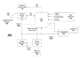
In one embodiment, device 101 allows a user to interact (e.g., effect cursor movement, scrolling, or button action) with a host via a wireless connection. Intended movement relevant to device 101 is optically sensed and translated into position data, and is communicated to the host receiver (e.g., computer) via the wireless connection. Device 101 can be, for example, a wireless optical mouse where the mouse is moved over surface 105 to effect the likes of cursor movement and scrolling on a screen associated with a computer to which the mouse is wirelessly coupled. Light from LED 110 reflects off surface 105 as the mouse moves, and the reflected light is focused on a photo-sensitive element of the optical sensor via a lens. In such an embodiment, surface 105 could be any surface such as a table top, sheet of paper, book cover, wall, brief case or mouse pad. Alternatively, surface 105 could be a surface such as a hand, forearm, leg or chest of a user. The point here is that device 101 will work on many diverse surfaces 105 and need not be limited to a special mouse pad or other dedicated surface. Such an embodiment of device 101 is thus independent of surface 105.
In an alternative embodiment, device 101 can be integrated into a wireless keyboard where device 101 generally remains stationary while cursor movement is effected by the likes of a stylus or human finger moving across surface 105. In such an embodiment, surface 105 might be a window that is proximally located to a lens of optical sensor 115. Light from LED 110 reflects off the object as the object moves across surface 105, and the reflected light is focused on a photo-sensitive element of the optical sensor via the lens. Intended movement across surface 105 is thus detected by optical sensor 115, translated into position data, and communicated to the host receiver via the wireless connection. In this type of embodiment, device 101 can include surface 105.
Regardless of whether device 101 is moved across an independent surface 105, or remains stationary while an external object is moved across a surface 105 of device 101, any resulting movement is detected, analyzed and translated into position data that (if appropriate) is communicated to the host (e.g., game console) via the wireless connection.
Note that the present invention need not be limited to computer input devices, but can be applied to any device requiring power management in order to prolong the life of a limited power source (e.g., a battery). For example, cell phones, pagers, personal digital assistants, or any electronic device associated with a power use scheme that can be characterized by a number of modes of awareness (based on factors such as the quantitative and qualitative nature of input stimulus and established patterns of use) can employ the techniques described herein. As such, the present invention is not intended to be limited to any one embodiment or configuration of components. Rather, numerous wireless device-types and component configurations can employ the present invention. For instance, any wireless devices employing power intensive technology, such as optical technology, laser technology, and interferometry technology can employ the present invention.
Components
The voltage output of power source 145 is regulated by power regulator 140. In one embodiment, power regulator 140 is a conventional DC to DC converter that converts a DC voltage output of power source 145 to a particular voltage (e.g., 3.2 volts DC), and provides that voltage to various components of device 101. For example, in the embodiment shown, the output of power regulator 140 is provided to optical sensor 115, MCU 120 and transmitter 130. As can be seen, the applied load varies depending on the state of switches 150 a and 150 b, which switch power to optical sensor 115 and transmitter 130, respectively. As such, power regulator 140 can also provide the necessary voltage regulation depending on factors such as varying load conditions and the voltage supply tolerance of the componentry being supplied power.
In one embodiment, transmitter 130 is a conventional radio frequency (RF) or microwave transmitter. In an alternative embodiment, transmitter 130 may be replaced by a conventional transceiver 130 (not shown) thereby allowing bi-directional communication between device 101 and a host system. In this application, device 101 might be an electronic device such as a personal digital assistant receiving a wireless communication from a host computer coupled to the Internet. For example, transceiver 130 may receive via antenna 135 an updated address book or an instruction set that can be stored in a RAM or non-volatile memory such as an electronically erasable programmable ROM or flash memory included in MCU 120. Likewise, an e-mail message might be received for viewing on a display associated with device 101. Such communication information can be demodulated and filtered by transceiver 130, and then provided to the corresponding I/O port of MCU 120 for any necessary processing.
In addition, the receiver circuit of transceiver 130 can be configured to receive communication information from a number of different host-types. In such an embodiment, transceiver 130 might include a dedicated antenna 135 and physical layer (not shown) for each type of host that is supported. For instance, a first host may be a Bluetooth-based cell phone and a second host might be a RF-based signaling device. Such a signaling device might be, for example, configured to detect stock prices as they are posted on Internet accessible resources. If the signaling device detects a strike price on a particular stock, it can transmit an RF signal to device 101 thereby alerting the user that action must be taken (e.g., a buy/sell indication). Regardless of the type of communication information received by transceiver 130, switch 150 b should remain closed during the time period when such communication information is expected to be received. Thus, a time schedule of expected transmissions to device 101 can be provided to MCU 120. MCU 120 can then control the state of switch 150 b based on the provided time schedule. Alternatively, switch 150 b can always remain closed when device 101 is capable of receiving communication information.
In one embodiment, image difference data is generated by optical sensor 115, where each pixel of a CCD array included in optical sensor 115 corresponds to a bit of a bit vector. An image reflected onto the CCD array causes a number of the pixels to turn on. A pixel that is on might correspond to a bit that is a logical one, while a pixel that is off might correspond to a bit that is a logical low. As such, each detected image can be represented by a bit vector. The bit vectors corresponding to consecutive detected images can be logically XORed (exclusive OR operation). The result of the XOR operation represents the image difference data. Other logical operations can be used to determine image difference data as well. Such image difference data is in binary form and therefore can be readily analyzed and processed by, for example, an algorithm running in MCU 120. Likewise, such image difference data can be readily translated into the likes of cursor position data, or scrolling direction and distance data by optical sensor 115 or MCU 120.
In alternative embodiments, optical sensor 115 can be replaced by other sensing-type components 116 or assemblies for sensing the likes of movement, vibration, drift or other activity associated with a wireless device or system. For example, interferometers, velocimeters, motion detectors and drift detectors can be employed in device 101 for sensing such activity.
Another way to control the power that is consumed by optical sensor 115 is by configuring optical sensor 115 with an internal switch that can be externally controlled. For example, the internal switch can be controlled by MCU 120 via bus 117. This internal switch of optical sensor 115 can be implemented, for example, in hardware, software, firmware, or any combination thereof. In a first state, the internal switch allows optical sensor 115 to operate in its native mode. In a second state, however, the native mode of optical sensor 115 is disabled thereby allowing external control of optical sensor 115. For instance, a number of algorithms running in MCU 120 can be programmed to effect a comprehensive power management scheme on optical sensor 115. Bus 117 can be used to facilitate communication between MCU 120 and optical sensor 115. In one embodiment, bus 117 is a serial peripheral interface bus (SPI), but other suitable bus technologies and protocols can be implemented here as well.
Another way to control the power that is consumed by optical sensor 115 is by opening and closing switch 150 a. Like switch 150 b, switch 150 a can be a metal oxide semiconductor (MOS) type switch, and has a control line that is coupled to an I/O port of MCU 120. Switch 150 a can alternatively be integrated into MCU 120, or implemented via an I/O port of MCU 120. Other switch types having a state (e.g., open or closed) that is responsive to a control line can be used here as well. By opening switch 150 a, all power to optical sensor 115 is completely removed thereby eliminating further power consumption by optical sensor 115. Once MCU 120 determines that optical sensor 115 needs power (e.g., based on data received from user interface 125), switch 150 a can be closed accordingly.
In one embodiment, MCU 120 implements a power management scheme that is characterized by various modes of awareness based on, for example, input stimuli and statistical analysis. Input stimuli are provided to MCU 120 by user interface 125 and by optical sensor 115. MCU 120 analyzes the input stimuli, determines the mode of awareness in which device 101 will operate in response to the input stimuli, and provides data derived from that input stimuli to transmitter 130. If device 101 includes a transceiver 130 (in lieu of transmitter 130), MCU 120 can also receive other communication information from transceiver 130 as explained above.
In addition, device 102 can alternatively include switch 150 c for switching power from power regulator 140 to MCU 120. Such an embodiment may be useful where MCU 120 is not configured with an internal low power mode as described above, or is otherwise associated with a power intensive profile (e.g., continuously operates at greater than 100 microamps). Switch 150 c has a state (e.g., open or closed) that depends on control line 157, which is derived from signals from the likes of signals from touch sensor 155, or user interface 125, or other sensing components or assemblies that sense user-based activity that indicates device 102 must apply power to MCU 120 and wake up (e.g., a dedicated “wake-up” button or sensor), or a combination thereof. One technique for providing control line 157 in response to such user-based activity is shown in FIG. 1 c, which will be discussed in turn.
Like switches 150 a and 150 b, switch 150 c can be a metal oxide semiconductor (MOS) type switch. Other switch types having a state (e.g., open or closed) that is responsive to a control line can be used here as well (e.g., a bipolar junction transistor-based switch). Switch 150 c can alternatively be integrated into touch sensor 155. By opening switch 150 c, all power to MCU 120 is completely removed thereby eliminating further power consumption by MCU 120. Once user-based activity is received control line 157 is activated, and switch 150 c is closed accordingly. In one embodiment, whether control line 157 is activated or not depends on whether touch sensor 155 is triggered thereby indicating the presence of a user. In such an embodiment, once touch sensor 155 triggers in response to the presence of a user (e.g., user is actually touching device 102 or is within one inch of touching device 102), control line 157 is activated thereby closing switch 150 c. Power from power regulator 140 is thus switched to MCU 120. On the other hand, if no user presence is reported by touch sensor 155, then control line 157 is deactivated and remains so until a trigger signal from touch sensor 155 is produced. When switch 150 c is deactivated, power to MCU 120 is switched out.
Note that control line 157 can be derived from a number of sources, whether from one or more touch sensors 155, one or more user interface elements from user interface 125, a dedicated “wake-up” button or sensor, or a combination thereof.
In general, touch sensor 155 is for sensing the touch or proximal presence of a user, and notifying MCU 120 accordingly. Thus, touch sensor 155 may be implemented in a number of technologies, including both direct touch sensing technology and proximity sensing technology that does not require actual contact. In addition, device 102 may include a number of touch sensors 155, each one being strategically located on or within device 102 (e.g., on the palm, index finger and thumb areas of a wireless optical mouse). As such, when device 102 is touched or approached by a user's hand or other appendage (e.g., finger, foot, forearm, stylus, prosthetic), any one or more of touch sensors 155 will trigger thereby notifying MCU 120 of the user's presence and intent to use device 102. In response, MCU 120 might modify the power mode of device 102. For instance, an algorithm running in MCU 120 might receive the output signal and transition the mode of operation of device 102 from a power saving mode to a full power run mode.
In one embodiment, touch sensor 155 is implemented using the circuitry of a touchpad or touch tablet that senses a users touch or pressure from a stylus or finger. Note that not all the circuitry or functionality of the touchpad or tablet need be employed. Rather, only the componentry for sensing the presence of a user and manifesting that presence as an electrical signal is needed. In such an embodiment, the presence of a user touch could be detected and manifested as a logical low signal at the output of touch sensor 155, which might normally be a logical high signal when there is no user touch. This output can be provided to an I/O port of MCU 120. Alternatively, touch sensor 155 can be implemented with a pressure sensitive switch that, when contacted by the user (hand, finger or otherwise) similarly generates a logical low signal at the output of touch sensor 155.
In an alternative embodiment, touch sensor 155 can be implemented with an electric field sensor that can detect the presence of human tissue (e.g., by way of resistance, capacitance or charge). In such an embodiment, the output signal of touch sensor 155 might be in one range (e.g., −50 to 50 microvolts) with no user presence, and a second range (e.g., 150 to 500 microvolts) during user presence. Regardless, MCU 120 would receive the output signal via an I/O port and act accordingly. Note that in such an embodiment, the user need not actually touch device 102 to trigger touch sensor 155. Rather, the proximal location of the user's hand to device 102 can be sufficient to trigger touch sensor 155 (e.g., within one inch of device 102).
Numerous other touch sensing technologies can be employed to realize touch sensor 155. For example, capacitive sensors, motion detectors, light level sensors, weight sensors, heat sensors and infrared detectors can be used alone or in combination to effect touch sensor 155. The type of technology selected for implementing touch sensor 155 depends on a number of factors such as power, cost, and space limitations associated with device 102. Regardless of what technology is used, the effect is that MCU 120 has access to user presence data, whether the user be physically touching device 102 or proximally touching device 102.
In another embodiment, a switch 150 d (not shown) similar to switches 150 a-c could be coupled between power source 145 and power regulator 140. Switch 150 d, which could alternatively be internal to power regulator 140, would allow power regulator 140 to be effectively switched to an off position thereby conserving power (e.g., even when there is no load on power regulator 140, it may still consume power). In such an embodiment, touch sensor 155 might be coupled directly to power source 145, and a trigger signal from touch sensor 155 could be used as a control line for controlling the state of switch 150 d. Alternatively, control line 157 could be used to control the state of switch 150 d, assuming that the components or assembly generating control line 157 can receive power directly from power source 145. Note that any one of switches 150 a, 150 b, and 150 c may or may not be included in an embodiment employing switch 150 d depending on factors such as the desired levels of power conservation.
Numerous other switching configurations for switching out components included in device 101 or 102 will be apparent in light of this disclosure. For descriptive purposes, switches 150 a-d are referred to as power switches because they switch in power.
Overview
The power management algorithm illustrated in FIG. 2 defines five modes of operation: run mode 205, walk mode 210, sleep mode 215, deep sleep mode 220 and hibernate mode 225. Run mode 205 is a full power mode, while walk mode 210, sleep mode 215, deep sleep mode 220 and hibernate mode 225 are time-staggered, power saving modes. Each of the power saving modes introduces power conserving measures that are more comprehensive than the previous power mode. For instance, walk mode 210 might conserve 75% power as compared to full power of run mode 205. Similarly, sleep mode 215 might conserve 90% power as compared to full power of run mode 205, while deep sleep mode 220 might conserve 95% power as compared to full power of run mode 205. Hibernate mode, on the other hand, might conserve 99% power as compared to full power of run mode 205.
As time advances without any sensed activity (thereby indicating lack of use of the associated wireless device), the device is transitioned from one power mode to the next power mode, until hibernate mode 225 is reached. In the embodiment shown, the power modes are transitioned in the following order during a period of inactivity: from run-mode 205 to walk mode 210 to sleep mode 215 to deep sleep mode 220 to hibernate mode 225. The time period allocated for a particular power mode to operate can be, for example, based on detection of inactivity or statistics. Likewise, the time period allocated for a particular mode to operate can be a preset time period (e.g., as measured by a timer included in MCU 120). A combination of such time periods can also be used.
For instance, the time period between run mode 205 and walk mode 210 can be based on an initial detection of inactivity. In such an embodiment, as long as there is continued activity, run mode 205 will be sustained. However, the mode of operation will transition from run mode 205 to walk mode 210 upon the first indication of inactivity (e.g., within 10 milliseconds of the inactive period's start). On the other hand, the walk mode time period 211 can be a preset time period (e.g., 1 minute of inactivity). The sleep mode time period 216 can also be a preset time period (e.g., 10 minutes of inactivity). The deep sleep mode time period 221 can be a preset time period initially (e.g., 3 hours of inactivity), but can later be refined to a different time period (e.g., ½ hour) based on statistical analysis and patterns of prior use. Such patterns of prior use can be, for example, monitored, stored and analyzed by MCU 120 as will be explained in turn.
Various modules of the algorithm can be programmed to receive activity data from user interface elements, or from an activity sensing device, assembly or circuit such as an optical sensor 115 or other activity sensing componentry that can provide data characterizing the sensed activity. In this way, the algorithm has access to data that is relevant to activity of the associated wireless device. The algorithm can then perform analysis (e.g., quantitative and qualitative) on the activity data to determine if a change in power mode is warranted by either inactivity or activity. Inactivity dictates the mode of operation be transitioned to the next power saving mode, while activity after a period of no activity dictates the mode of operation be transitioned to the to run mode 205.
Activity can be, for example, movement of an associated wireless device as detected by an optical sensor with reference to a surface (e.g., movement of a wireless optical mouse). Likewise, activity can be indicated by user interface elements, such as a button press or a wheel roll of a wireless optical mouse. The corresponding activity data might be a series of images or image difference data from an optical sensor included in the wireless device, or various logical signals from user interface elements of the wireless device.
Run Mode
The wireless device will operate in run mode 205 so long as there is sustained device activity. However, once a lack of activity is detected, the mode of operation transitions from run mode 205 to walk mode 210 as will now be explained.
Walk Mode
The walk mode module issues a walk data query 231 to the activity sensing device or assembly (e.g., optical sensor of wireless optical mouse). This data query 231 is seeking walk mode sensor data 230 in order to determine if run mode 205 should be transitioned to walk mode 210, or if walk mode 210 should be transitioned to run mode 205. Walk data query 231 is issued periodically. In one embodiment, walk data query 231 is issued approximately every 10 milliseconds, although other polling rates such as every 1 millisecond or every 50 milliseconds, can also be used depending on factors such as the desired device response time and the power of the processor running the algorithm. This polling rate effectively defines the time it takes for an associated wireless device to transition from walk mode 210 to run mode 205, or vice versa depending on walk mode sensor data 230.
In the embodiment shown, an optical sensor responds to each walk data query 231. The response includes walk mode sensor data 230. Walk mode sensor data 230 can be, for example, a series of images or image difference data generated by the optical sensor (e.g., optical sensor 115), and can be expressed as bit vectors to facilitate processing as explained above. The walk mode module can interrogate the received walk mode sensor data 230. For example, the walk mode module can compare the latest image data received with the previous image data received in order to determine the image difference data. Analysis of the image difference data can then be performed to determine if a power mode change is warranted. Alternatively, the walk mode module can just perform analysis if the polled walk mode sensor data 230 is already in the form of image difference data (e.g., optical sensor performed the difference operation). In one embodiment, the analysis performed by the walk mode module includes determining if the image difference data is a non-zero value thereby indicating movement. If movement is detected during walk mode 210, then the mode of operation transitions from walk mode 210 to run mode 205 as is explained below.
User interface-type data 245 of the wireless device, on the other hand, generally requires less or no analysis because it represents a distinct and deliberate act of the user, and is therefore less likely to be representative of false activity. Thus, if user interface-type data 245 is detected during walk mode 210, then the mode of operation transitions from walk mode 210 to run mode 205.
For the sake of clarity, false activity represents movement or other activity that was not intended by the user, or is atypical movement given the circumstances. For example, when a user unintentionally moves the mouse by bumping the surface upon which the mouse is resting, the resulting movement can be qualified as false activity. Likewise, if a period of substantial activity (e.g., mouse moved 5 centimeters to double-click on folder and then double-clicked document) is followed by a period of no activity (e.g., while user reads opened document), the next movement should likely be substantial (e.g., move to upper right corner to close document, or to select hypertext). If it is not substantial (e.g., less than 10 millimeters), then the resulting movement can be qualified as false activity. On the other hand, if the movement is substantial (e.g., greater than 10 millimeters), then the resulting movement can be qualified as true activity.
Transitions Between Walk and Run Modes
If the wireless device associated with the algorithm is operating in run mode 205, and no movement (e.g., as indicated by walk mode sensor data 230) or user interface-type data 245 is detected, then the walk mode module effectively disables run mode 205 by issuing a walk mode call 207, and the mode of operation accordingly transitions from run mode 205 to walk mode 210. Thus, the walk mode module is in full control of the device. In the context of a wireless device as illustrated in FIGS. 1 a and b, when the mode of operation is transitioned to walk mode 210, the native mode of optical sensor 115 is disabled, and switch 150 b is opened. As such, transmitter 130 is in its off state thereby conserving power. The mode of operation remains walk mode 210 until walk mode time period 211 expires, walk mode sensor data 230 indicates movement, or user interface-type data 245 is received.
If any movement (e.g., as indicated by walk mode sensor data 230) or any user interface-type data 245 is detected during walk mode 210, then the walk mode module issues run mode call 209 thereby enabling run mode 205, and the mode of operation accordingly transitions from walk mode 210 to run mode 205. The run mode module takes control of the device (or delegates that control to a “native mode”), switches transmitter 130 back in by closing switch 150 b, performs any necessary translation, and provides the translated data to transmitter 130 for transmission to the host receiver. The mode of operation remains run mode 205 so long as walk mode sensor data 230 indicates movement or user interface-type data 245 is being received. If the polled walk mode sensor data 230 indicates lack of movement and no user interface-type data 245 is being received during run mode 205, then the walk mode module disables run mode 205 by issuing walk mode call 207, and walk mode 210 takes over as described above.
In the event, however, that the mode of operation remains walk mode 210 until walk mode time period 211 expires, then the mode of operation transitions to sleep mode 215 as will now be explained.
Sleep Mode
The sleep mode module issues a sleep data query 236 to the activity sensing devices (e.g., optical sensor of wireless optical mouse). This data query 236 is seeking sleep mode sensor data 235 in order to determine if sleep mode 215 should be transitioned to run mode 205. Sleep data query 231 is issued periodically. In one embodiment, sleep data query 231 is issued approximately every 100 milliseconds, although other polling rates such as every 1 microsecond or every 500 milliseconds, can also be used depending on factors such as the desired device response time and the power of the processor running the algorithm. This polling rate effectively defines the time it takes for an associated wireless device to transition from sleep mode 215 to run mode 205 depending on sleep mode sensor data 235.
In the embodiment shown, an optical sensor responds to each sleep data query 236. This response includes sleep mode sensor data 235. Sleep mode sensor data 235 can be, for example, a series of images or image difference data generated by the optical sensor (e.g., optical sensor 115), and can be expressed as bit vectors to facilitate processing as explained above. The sleep mode module can interrogate the received sleep mode sensor data 235. The previous discussion with regards to image analysis performed by the walk mode module equally applies to the sleep mode module. In addition, if movement is detected, the analysis performed by the sleep mode module may further include qualifying the image difference so as to determine if the movement qualifies as true activity.
For instance, if the movement detected satisfies a predetermined threshold of quality (e.g., distance of movement is greater than 5 millimeters), then it is considered true activity and the mode of operation transitions from sleep mode 215 to run mode 205. Otherwise, the movement is considered false activity, and the mode of operation remains sleep mode 215. Likewise, an image difference comparison can be made thereby qualifying the degree to which the images are different. The greater the degree of difference between the images, the more likely that true activity has been sensed. On the other hand, the greater the similarity between the images, the more likely that false activity has been sensed. For example, if more than 25% of the pixels associated with one image have values that are different from the values of the corresponding pixels associated with a consecutive image, then true activity is sensed and the mode of operation transitions from sleep mode 215 to run mode 205. Otherwise, the movement is considered false activity, and the mode of operation remains sleep mode 215. The degree of difference between images that indicates true activity depends on factors such as the resolution and sensitivity of the sensing device, the sensing area (e.g., size and shape) and the desired performance of the associated device.
If user interface-type data 245 is detected during sleep mode 215, on the other hand, no qualification is necessary and the mode of operation transitions from sleep mode 215 to run mode 205.
Transitions From Sleep to Run Mode
If the wireless device associated with the algorithm is operating in sleep mode 215, and no movement (e.g., as indicated by sleep mode sensor data 235) or user interface-type data 245 is detected, then the sleep mode module is in full control of the device. In the context of a wireless device as illustrated in FIGS. 1 a and b, when the mode of operation is sleep mode 215, the native mode of optical sensor 115 is disabled, and switch 150 b is opened. As such, transmitter 130 is in its off state thereby conserving power. The mode of operation remains sleep mode 215 until sleep mode time period 216 expires, sleep mode sensor data 235 indicates movement that qualifies as true activity, or user interface-type data 245 is received.
If qualified movement (e.g., as indicated by sleep mode sensor data 235) or any user interface-type data 245 is detected during sleep mode 215, then the sleep mode module issues sleep mode wake-up call 214 thereby enabling run mode 205, and the mode of operation accordingly transitions from sleep mode 215 to run mode 205. The run mode module then takes control of the device and proceeds as previously explained.
In the event, however, that the mode of operation remains sleep mode 215 until sleep mode time period 216 expires, then the mode of operation transitions to deep sleep mode 220 as will now be explained.
Deep Sleep Mode
The deep sleep mode module issues a deep sleep data query 241 to the activity sensing devices (e.g., optical sensor of wireless optical mouse). This data query 241 is seeking deep sleep mode sensor data 240 in order to determine if deep sleep mode 220 should be transitioned to run mode 205. Deep sleep data query 241 is issued periodically. In one embodiment, deep sleep data query 241 is issued approximately every 1 second, although other polling rates such as every 400 milliseconds or every 2 seconds, can also be used depending on factors such as the desired device response time and the power of the processor running the algorithm. This polling rate effectively defines the time it takes for an associated wireless device to transition from deep sleep mode 220 to run mode 205 depending on deep sleep mode sensor data 240.
In the embodiment shown, an optical sensor responds to each deep sleep data query 241. This response includes deep sleep mode sensor data 240. Deep sleep mode sensor data 240 can be, for example, a series of images or image difference data generated by the optical sensor (e.g., optical sensor 115), and can be expressed as bit vectors to facilitate processing as explained above. The deep sleep mode module can interrogate the received deep sleep mode sensor data 240. The previous discussion with regards to image analysis performed by the walk mode module equally applies to the deep sleep mode module. In addition, if movement is detected, the analysis performed by the deep sleep mode module may further include determining the distance and direction of the movement so as to determine if the movement qualifies as true activity. For instance, if the movement detected satisfies a predetermined threshold of quality (e.g., distance of movement is greater than 10 millimeters), then it is considered true activity and the mode of operation transitions from deep sleep mode 220 to run mode 205. Otherwise, the movement is considered false activity, and the mode of operation remains deep sleep mode 220. Likewise, an image difference comparison can be made thereby qualifying the degree to which the images are different. For example, if more than 33% of the pixels associated with one image have values that are different from the values of the corresponding pixels associated with a consecutive image, then true activity is sensed and the mode of operation transitions from deep sleep mode 220 to run mode 205. Otherwise, the movement is considered false activity, and the mode of operation remains deep sleep mode 220. Note that the predetermined threshold of quality associated with deep sleep mode 220 is more stringent than the predetermined threshold of quality associated with sleep mode 215. As such, transitioning from deep sleep mode 220 to run mode 205 is effectively more difficult than transitioning from sleep mode 215 to run mode 205.
Alternatively, deep sleep mode 220 can have a predetermined threshold of quality that is the same as that of sleep mode 215. Note, however, that the reaction time for transitioning from deep sleep mode 220 to run mode 205 (based on polling rate of deep sleep sensor data 240) is longer than the reaction time for transitioning from sleep mode 215 to run mode 205 (based on polling rate of sleep sensor data 235).
User interface-type data 245 detected during deep sleep mode 220 can also be qualified. For instance, button clicks and wheel movement translating to more than 5 millimeters of scrolling can be qualified as true activity, and the mode of operation transitions from deep sleep mode 220 to run mode 205. On the other hand, wheel movement translating to less than 5 millimeters of scrolling can be qualified as false activity and ignored. Thus, the mode of operation remains deep sleep mode 220.
Transitions From Deep Sleep to Run Mode
If the wireless device associated with the algorithm is operating in deep sleep mode 220, and no movement (e.g., as indicated by deep sleep mode sensor data 240) or user interface-type data 245 is detected, then the deep sleep mode module is in full control of the device. In the context of a wireless device as illustrated in FIGS. 1 a and b, when the mode of operation is deep sleep mode 220, the native mode of optical sensor 115 is disabled, and switch 150 b is opened. As such, transmitter 130 is in its off state thereby conserving power. The mode of operation remains deep sleep mode 220 until deep sleep mode time period 221 expires, deep sleep mode sensor data 240 indicates movement that qualifies as true activity, or user interface-type data 245 that qualifies as true activity is received.
If qualified movement (e.g., as indicated by deep sleep mode sensor data 240) or qualified user interface-type data 245 is detected during deep sleep mode 220, then the deep sleep mode module issues deep sleep mode wake-up call 219 thereby enabling run mode 205, and the mode of operation accordingly transitions from deep sleep mode 220 to run mode 205. The run mode module then takes control of the device and proceeds as previously explained.
In the event, however, that the mode of operation remains deep sleep mode 220 until deep sleep mode time period 221 expires, then the mode of operation is transitioned to hibernate mode 225 as will now be explained.
Hibernate Mode
For example, button clicks can be qualified as true activity, and the mode of operation transitions from hibernate mode 225 to run mode 205. On the other hand, wheel movement of any kind can be qualified as false activity and ignored. Thus, the mode of operation remains hibernate mode 225.
Transitions from Hibernate to Run Mode
If the wireless device associated with the algorithm is operating in hibernate mode 225, and no user interface-type data 245 is detected, then the hibernate mode module is in full control of the device. In the context of a wireless device as illustrated in FIGS. 1 a and b, when the mode of operation is hibernate mode 225, the native mode of optical sensor 115 is disabled, and switches 150 a and 150 b are opened. As such, optical sensor 115 and transmitter 130 are in their off states thereby conserving power. If included, switch 150 c can also be opened thereby switching MCU 120 to its off state for additional power conservation. Likewise, if included, switch 150 d can also be opened thereby switching power regulator 140 to its off state for additional power conservation. The mode of operation remains hibernate mode 225 until interface-type data 245 that qualifies as true activity is received.
If qualified user interface-type data 245 is detected during hibernate mode 225, then the hibernate mode module issues hibernate mode wake-up call 224 thereby enabling run mode 205, and the mode of operation accordingly transitions from hibernate mode 225 to run mode 205. The run mode module then takes control of the device and proceeds as previously explained.
Qualifying Activity as True or False Based on Statistical Analysis
As previously stated, activity data resulting from movement can be qualified as true or false activity based on distance and or direction of movement. Likewise, movement can also be qualified as true or false activity based on statistical or historical data. Such data can be used to define patterns of use for the associated wireless device. Some patterns or types of use are unique to a specific user, while other patterns or types of use can be generically applied to a large group of people (e.g., mouse users).
For instance, most mouse users stop moving the mouse shortly after double-clicking to perform the likes of opening a document or executing an application. As such, movement following a period of inactivity after a double-click will likely be substantial (e.g., greater than 10 millimeters). For the sake of discussion, assume that the last user action involving a wireless optical mouse was a double-click (e.g., to open or execute) immediately followed by a move (e.g., to move cursor out of way). If the next move is less than 10 millimeters, then the move could be qualified as false activity. Such a statistical-based qualification can be used to complement or override a quantity-based qualification.
For example, recall that any detected movement in walk mode 210 can cause run mode 205 to be enabled. However, if a slight movement (e.g., 5 millimeters) is detected during walk mode 210 after a period of inactivity following a double-click, then such a movement can be qualified a false activity. Thus, a statistical-based qualification relevant to a particular type of use (e.g., movement after a double-click action of a mouse) can override a quantity-based qualification relevant to a less specific type of use (e.g., any movement). Patterns or types of use that are unique to a specific user can also be used to complement or override quantity-based qualifications. Generally, a user's use of a device can be broken down into sessions, and each session can be further broken down into stages (e.g., an active stage, a semi-active stage and inactive stage). Each stage can, for example, can be associated with a mode of operation of the power management algorithm. For instance, the active stage can correspond to run mode 205 and walk mode 210, the semi-active stage can correspond to sleep mode 215 and deep sleep mode 220, and the inactive stage can correspond to hibernate mode 225. The time that each power mode is sustained can be monitored by a MCU of the associated wireless device, and stored in a non-volatile memory accessible by the MCU (or included in the MCU). After a number of sessions, average times and statistics can be determined.
Such average times and statistics effectively define a usage envelope of the associated wireless device. For example, a wireless optical mouse associated with a particular household or user might have the following usage envelope: (1) the mouse is generally never used before 6 a.m. or after 12 a.m.; (2) the average walk mode time period 211 is 65 seconds; and (3) the average sleep mode time period 216 is 6 minutes; (3) the average deep sleep mode time period 221 is 45 minutes. Recorded statistics might further indicate that: (A) out of 120 hours of total use, only 2 minutes of use were between 12 a.m. and 6 a.m.; (B) out of 75 transitions from sleep mode 215 to run mode 205, 72 occurred within 9 minutes; and (C) out of 46 transitions from deep sleep mode 220 to run mode 205, 44 occurred within 25 minutes.
Such average times and statistics can be used to qualify future activity of the associated wireless mouse. For example, assume that the mouse is in deep sleep mode 220 and the time is 12:30 a.m. Shortly thereafter, an earthquake moves the mouse 15 millimeters. Assume that the quantity-based qualification to transition from deep sleep mode 220 to run mode requires a move of 10 millimeters or more. However, the a statistical-based qualification complements the quantity-based qualification by considering the timeliness of the move. In this case, a move of 20 millimeters or more between the hours of 12 a.m. and 6 a.m. is required to transition the mouse from deep sleep mode 220 to run mode 205. As such, the mouse remains in deep sleep mode 220 despite the earthquake.
Similarly, assume that the time is 1:30 p.m. and the mouse has been in deep sleep mode 220 for 40 minutes. Shortly thereafter, a cat residing in the household chases a real mouse across the desktop where the wireless optical mouse is resting. Although graceful in its approach, the cat bumps the wireless optical mouse causing it to move 10 millimeters. Again, assume that the quantity-based qualification to transition from deep sleep mode 220 to run mode requires a move of 10 millimeters or more. However, the statistical-based qualification complements the quantity-based qualification by considering the statistic that, if the mouse is going to come out of deep sleep mode, it will do so within 25 minutes over 95% of the time (e.g., 44/46 transitions). In this case, where the wireless optical mouse has been in deep sleep mode 220 for over 30 minutes, a move of 15 millimeters or more is required to transition the mouse from deep sleep mode 220 to run mode 205. As such, the wireless optical mouse remains in deep sleep mode 220 while the cat enjoys a late lunch.
Overview
The power management algorithm illustrated in FIG. 3 is similar to the power management algorithm discussed with reference to FIG. 2 . In this embodiment, however, the algorithm defines only three modes of operation: run mode 205, walk mode 210, and hibernate mode 225. The power modes are transitioned in the following order during a period of inactivity: from run-mode 205 to walk mode 210 to hibernate mode 225. The time period between run mode 205 and walk mode 210 can be based on an initial detection of inactivity, while the walk mode time period 211 can be a preset time period (e.g., 2 minutes of inactivity). In addition, Walk mode time period 211 can later be refined to a different time period (e.g., 1 minute of inactivity) based on statistical analysis and patterns of prior use.
Run Mode
Walk Mode
Hibernate Mode
The hibernate mode module issues a hibernate data query 307 to the activity sensing devices (e.g., touch sensor 155). This data query 307 is seeking hibernate mode sensor data 305 in order to determine if hibernate mode 225 should be transitioned to run mode 205. Hibernate data query 307 is issued periodically. In one embodiment, hibernate data query 307 is issued approximately every 1 second, although other polling rates such as every 10 milliseconds or every 10 seconds, can also be used depending on factors such as the desired device response time and the power of the processor running the algorithm. This polling rate effectively defines the time it takes for an associated wireless device to transition from hibernate mode 225 to run mode 205 depending on hibernate mode sensor data 305.
In the embodiment shown, a sensor responds to each hibernate data query 307. This response includes hibernate mode sensor data 305. Hibernate mode sensor data 305 can be, for example, a signal from a touch sensor that is triggered by the charge, resistance, or capacitance of human tissue. If such a signal is received thereby indicating that the associated device is being touched, then the mode of operation transitions from hibernate mode 225 to run mode 205. Otherwise, the mode of operation remains hibernate mode 225. User interface-type data 245 detected during hibernate mode 225 can be qualified. For instance, button clicks and wheel movement translating to more than 5 millimeters of scrolling can be qualified as true activity, and the mode of operation transitions from hibernate mode 225 to run mode 205. On the other hand, wheel movement translating to less than 5 millimeters of scrolling can be qualified as false activity and ignored. Thus, the mode of operation remains hibernate mode 225.
In an alternative embodiment, hibernate mode sensor data 305 can be essentially included in user interface-type data 245. In such an embodiment, activity data (whether hibernate mode sensor data 305 or user interface-type data 245) would automatically be provided to the MCU when such data became available. Thus, no polling would be necessary (e.g., no need to periodically issue hibernate data query 307). As such, hibernate mode 225 could employ an additional power saving measure by switching out the MCU. The associated switch (e.g., 150 c) could be opened during the hibernate mode, and closed in response to a run mode 205 enabling event (e.g., trigger signal from a touch sensor or a user interface element).
Transitions Between Hibernate and Run Modes
If the wireless device associated with the algorithm is operating in hibernate mode 225, and no hibernate mode sensor data 305 or user interface-type data 245 is detected, then the hibernate mode module is in full control of the device. In the context of a wireless device as illustrated in FIGS. 1 a and b, when the mode of operation is hibernate mode 225, the native mode of optical sensor 115 is disabled, and switches 150 a and 150 b are opened. As such, optical sensor 115 and transmitter 130 are in their off states thereby conserving power. If included, switch 150 c can be opened to switch MCU 120 to its off state for additional power conservation. Likewise, if included, switch 150 d can be opened to switch power regulator 140 to its off state for additional power conservation. The mode of operation remains hibernate mode 225 until hibernate mode sensor data 305 indicates the touch of a user, or user interface-type data 245 that qualifies as true activity is received.
If hibernate mode sensor data 305 indicates the presence of a user, or qualified user interface-type data 245 is detected during hibernate mode 225, then the hibernate mode module issues hibernate mode wake-up call 224 thereby enabling run mode 205, and the mode of operation accordingly transitions from hibernate mode 225 to run mode 205. The run mode module then takes control of the device and proceeds as previously explained.
The foregoing description of the embodiments of the invention has been presented for the purposes of illustration and description. It is not intended to be exhaustive or to limit the invention to the precise form disclosed. Many modifications and variations are possible in light of the above teaching. For example, in the above description, the walk mode module detects lack of motion and user interface-type data, and disables run mode 205 by issuing walk mode call 207. In an alternative embodiment, run mode 205 can have access to sensor data (e.g., run mode sensor data) and user interface-type data thereby allowing run mode 205 to detect lack of motion and user interface-type data. In such an embodiment, rather than having walk mode 210 disable run mode 205 by issuing a walk mode call 207, run mode 205 could effectively disable itself by issuing the walk mode call 207 to the walk mode module, and the mode of operation would transition from run mode 205 to walk mode 210. It is intended that the scope of the invention be limited not by this detailed description, but rather by the claims appended hereto.
Claims (20)
1. An optical sensing assembly for a computer input device configured to receive power from a self-contained power source, the optical sensing assembly comprising:
a photo-sensitive element configured to receive reflected light from a light source to produce first image data associated with a first image and second image data associated with a second image;
an image data processing logic coupled to the photo-sensitive element and configured to detect activity based on the first and second image data and to determine whether the detected activity qualifies as false activity based on a prior activity and a stored pattern of a plurality of activities; and
a power control logic operatively coupled to the image data processing logic and configured to implement a native power control mode wherein an internal algorithm changes the power consumption of the optical sensing assembly from a full power mode to one or more lower power modes based on the determination of whether the detected activity qualifies as false activity.
2. The optical sensing assembly of claim 1 , wherein the photo-sensitive element is one of a CCD array or a photo diode.
3. The optical sensing assembly of claim 2 , wherein the photo-sensitive element is a CCD array having a set of pixels and the first and second image data comprises a bit vector corresponding to a set of states of the set of pixels.
4. The optical sensing assembly of claim 1 , further comprising a focusing lens coupled to the photo-sensitive element for focusing the reflected light to the photo-sensitive element.
5. The optical sensing assembly of claim 1 , wherein the image data processing logic is further configured to translate image difference data to one of position data or displacement distance data, the image difference data determined from differences between the first image data and the second image data.
6. The optical sensing assembly of claim 1 , wherein determining whether the detected activity qualifies as false activity comprises:
comparing the prior activity and detected activity to the stored pattern.
7. The optical sensing assembly of claim 1 , wherein a determination is made that the detected activity qualifies as false activity responsive to the detected activity and the prior activity not matching the stored pattern.
8. The optical sensing assembly of claim 1 , wherein the stored pattern is determined by tracking activities of a user of a computer input device.
9. A method for detecting movement with a photo sensing device configured to receive power from a self-contained power source, the method comprising:
determining image difference data from differences between first image data and second image data;
detecting activity based on the image difference data;
determining whether the detected activity qualifies as false activity based on a prior activity and a stored pattern of a plurality of activities; and
implementing a native power control mode wherein an internal algorithm changes the power consumption of the photo-sensing device from a full power mode to one or more lower power modes based on the determination of whether the detected activity qualifies as false activity.
10. The method of claim 9 , wherein one or more photo diodes produce the first and second image data based on reflected light.
11. The method of claim 9 , wherein a CCD array having a set of pixels produces the first and second image data based on reflected light, the first and second image data comprising a bit vector corresponding to a set of states of the set of pixels.
12. The method of claim 9 , wherein a determination is made that the detected activity qualifies as false activity responsive to the detected activity and the prior activity not matching the stored pattern.
13. The method of claim 9 , wherein the stored pattern is determined by tracking activities of a user of a computer input device.
14. The method of claim 9 , wherein the stored pattern describes a series of activities that are considered true activities.
15. A non-transitory computer readable storage medium having computer program instructions and data embodied thereon, the computer program instructions and data to configure a processor to perform operations comprising:
determining image difference data from differences between first image data and second image data;
detecting activity based on the image difference data;
determining whether the detected activity qualifies as false activity based on a prior activity and a stored pattern of a plurality of activities; and
implementing a native power control mode wherein an internal algorithm changes the power consumption of the photo-sensing device from a full power mode to one or more lower power modes based on the determination of whether the detected activity qualifies as false activity.
16. The non-transitory computer readable storage medium of claim 15 , wherein one or more photo diodes produce the first and second image data based on reflected light.
17. The non-transitory computer readable storage medium of claim 15 , wherein a CCD array having a set of pixels produces the first and second image data based on reflected light, the first and second image data comprising a bit vector corresponding to a set of states of the set of pixels.
18. The non-transitory computer readable storage medium of claim 15 , wherein a determination is made that the detected activity qualifies as false activity responsive to the detected activity and the prior activity not matching the stored pattern.
19. The non-transitory computer readable storage medium of claim 15 , wherein the stored pattern is determined by tracking activities of a user of a computer input device.
20. The non-transitory computer readable storage medium of claim 15 , wherein the stored pattern describes a series of activities that are considered true activities.
Priority Applications (1)
| Application Number | Priority Date | Filing Date | Title |
|---|---|---|---|
| US12/179,490 US8207940B2 (en) | 2000-11-09 | 2008-07-24 | Wireless optical input device |
Applications Claiming Priority (3)
| Application Number | Priority Date | Filing Date | Title |
|---|---|---|---|
| US09/709,046 US6781570B1 (en) | 2000-11-09 | 2000-11-09 | Wireless optical input device |
| US10/809,626 US7425945B2 (en) | 2000-11-09 | 2004-03-24 | Wireless optical input device |
| US12/179,490 US8207940B2 (en) | 2000-11-09 | 2008-07-24 | Wireless optical input device |
Related Parent Applications (1)
| Application Number | Title | Priority Date | Filing Date |
|---|---|---|---|
| US10/809,626 Continuation US7425945B2 (en) | 2000-11-09 | 2004-03-24 | Wireless optical input device |
Publications (2)
| Publication Number | Publication Date |
|---|---|
| US20090027341A1 US20090027341A1 (en) | 2009-01-29 |
| US8207940B2 true US8207940B2 (en) | 2012-06-26 |
Family
ID=24848253
Family Applications (3)
| Application Number | Title | Priority Date | Filing Date |
|---|---|---|---|
| US09/709,046 Expired - Lifetime US6781570B1 (en) | 2000-11-09 | 2000-11-09 | Wireless optical input device |
| US10/809,626 Expired - Lifetime US7425945B2 (en) | 2000-11-09 | 2004-03-24 | Wireless optical input device |
| US12/179,490 Expired - Lifetime US8207940B2 (en) | 2000-11-09 | 2008-07-24 | Wireless optical input device |
Family Applications Before (2)
| Application Number | Title | Priority Date | Filing Date |
|---|---|---|---|
| US09/709,046 Expired - Lifetime US6781570B1 (en) | 2000-11-09 | 2000-11-09 | Wireless optical input device |
| US10/809,626 Expired - Lifetime US7425945B2 (en) | 2000-11-09 | 2004-03-24 | Wireless optical input device |
Country Status (3)
| Country | Link |
|---|---|
| US (3) | US6781570B1 (en) |
| CN (2) | CN1207646C (en) |
| DE (1) | DE10155044B4 (en) |
Cited By (2)
| Publication number | Priority date | Publication date | Assignee | Title |
|---|---|---|---|---|
| US20110109553A1 (en) * | 2009-11-10 | 2011-05-12 | Tsao Chih-Ming | Wireless touchpad mouse |
| US20120198258A1 (en) * | 2011-02-02 | 2012-08-02 | Avago Technologies Ecbu Ip (Singapore) Pte. Ltd. | Wireless input device with a power saving system |
Families Citing this family (134)
| Publication number | Priority date | Publication date | Assignee | Title |
|---|---|---|---|---|
| US9513744B2 (en) | 1994-08-15 | 2016-12-06 | Apple Inc. | Control systems employing novel physical controls and touch screens |
| US8228305B2 (en) | 1995-06-29 | 2012-07-24 | Apple Inc. | Method for providing human input to a computer |
| US8610674B2 (en) | 1995-06-29 | 2013-12-17 | Apple Inc. | Programmable tactile touch screen displays and man-machine interfaces for improved vehicle instrumentation and telematics |
| US8482535B2 (en) | 1999-11-08 | 2013-07-09 | Apple Inc. | Programmable tactile touch screen displays and man-machine interfaces for improved vehicle instrumentation and telematics |
| US8576199B1 (en) | 2000-02-22 | 2013-11-05 | Apple Inc. | Computer control systems |
| US6781570B1 (en) * | 2000-11-09 | 2004-08-24 | Logitech Europe S.A. | Wireless optical input device |
| TWI234710B (en) * | 2001-04-16 | 2005-06-21 | Wistron Corp | Wireless data process System and method |
| JP4027616B2 (en) * | 2001-04-20 | 2007-12-26 | 三菱電機株式会社 | Pointing device device and mobile phone |
| US6816154B2 (en) * | 2001-05-30 | 2004-11-09 | Palmone, Inc. | Optical sensor based user interface for a portable electronic device |
| US20050007345A1 (en) * | 2002-02-26 | 2005-01-13 | Yen-Liang Kuan | Power saving device |
| US20030197677A1 (en) * | 2002-04-17 | 2003-10-23 | Hulvey Robert W. | Keyboard/mouse/GPIO interface of a wireless interface device |
| TW577012B (en) * | 2002-04-17 | 2004-02-21 | Lite On Technology Corp | Power saving device and method of wireless mouse |
| US6920574B2 (en) * | 2002-04-29 | 2005-07-19 | Apple Computer, Inc. | Conserving power by reducing voltage supplied to an instruction-processing portion of a processor |
| EP1532670A4 (en) * | 2002-06-07 | 2007-09-12 | Praesagus Inc | Characterization adn reduction of variation for integrated circuits |
| US7152215B2 (en) * | 2002-06-07 | 2006-12-19 | Praesagus, Inc. | Dummy fill for integrated circuits |
| US7393755B2 (en) * | 2002-06-07 | 2008-07-01 | Cadence Design Systems, Inc. | Dummy fill for integrated circuits |
| US7124386B2 (en) * | 2002-06-07 | 2006-10-17 | Praesagus, Inc. | Dummy fill for integrated circuits |
| US20030229875A1 (en) * | 2002-06-07 | 2003-12-11 | Smith Taber H. | Use of models in integrated circuit fabrication |
| US7363099B2 (en) * | 2002-06-07 | 2008-04-22 | Cadence Design Systems, Inc. | Integrated circuit metrology |
| TW562326U (en) * | 2002-11-07 | 2003-11-11 | Globlink Technology Inc | Power saving mechanism of wireless electric appliance |
| GB0216635D0 (en) * | 2002-07-17 | 2002-08-28 | Cambridge Silicon Radio Ltd | Detecting device usage |
| US6954867B2 (en) * | 2002-07-26 | 2005-10-11 | Microsoft Corporation | Capacitive sensing employing a repeatable offset charge |
| US20040021586A1 (en) * | 2002-07-31 | 2004-02-05 | Wenkwei Lou | Keyboard scanner with error rejection |
| US20040021632A1 (en) * | 2002-07-31 | 2004-02-05 | Wenkwei Lou | High performance, low power key matrix scanner |
| US20040021635A1 (en) * | 2002-07-31 | 2004-02-05 | Wenkwei Lou | Error rejection for optical scroll wheel |
| US20040024927A1 (en) * | 2002-07-31 | 2004-02-05 | Hulvey Robert W. | High performance scanner for user input devices |
| US7363039B2 (en) | 2002-08-08 | 2008-04-22 | Qualcomm Incorporated | Method of creating and utilizing diversity in multiple carrier communication system |
| US8190163B2 (en) | 2002-08-08 | 2012-05-29 | Qualcomm Incorporated | Methods and apparatus of enhanced coding in multi-user communication systems |
| US6961595B2 (en) | 2002-08-08 | 2005-11-01 | Flarion Technologies, Inc. | Methods and apparatus for operating mobile nodes in multiple states |
| US7152111B2 (en) * | 2002-08-15 | 2006-12-19 | Digi International Inc. | Method and apparatus for a client connection manager |
| KR100702746B1 (en) * | 2002-08-20 | 2007-04-03 | 엘지전자 주식회사 | Method and apparatus for managing power of wireless local area network module in computer system |
| US7358963B2 (en) * | 2002-09-09 | 2008-04-15 | Apple Inc. | Mouse having an optically-based scrolling feature |
| US7102617B2 (en) * | 2002-12-30 | 2006-09-05 | Motorola, Inc. | Compact optical pointing apparatus and method |
| US6995748B2 (en) * | 2003-01-07 | 2006-02-07 | Agilent Technologies, Inc. | Apparatus for controlling a screen pointer with a frame rate based on velocity |
| US20040213140A1 (en) * | 2003-01-31 | 2004-10-28 | Taylor John W. | Interactive electronic device with optical page identification system |
| US7199783B2 (en) * | 2003-02-07 | 2007-04-03 | Avago Technologies Ecbu Ip (Singapore) Pte. Ltd. | Wake-up detection method and apparatus embodying the same |
| MXPA05008892A (en) | 2003-02-19 | 2006-05-25 | Qualcomm Flarion Tech | Controlled superposition coding in multi-user communication systems. |
| US7030771B2 (en) * | 2003-03-12 | 2006-04-18 | Sun Microsystems, Inc. | System and method to provide hot-swap status indication in a computer system having redundant power supplies |
| TWI225982B (en) * | 2003-03-18 | 2005-01-01 | Jeng-Shiung Chen | Power shutdown method of wireless peripheral device |
| US7310498B2 (en) * | 2003-04-09 | 2007-12-18 | Standard Microsystems Corporation | Communication protocol for personal computer system human interface devices over a low bandwidth, bi-directional radio frequency link |
| US20040203480A1 (en) * | 2003-04-09 | 2004-10-14 | Dutton Drew J. | Configuration and management of human interface and other attached devices through bi-directional radio frequency link |
| US7055047B2 (en) * | 2003-04-09 | 2006-05-30 | Standard Microsystems Corporation | Selective implementation of power management schemes based on detected computer operating environment |
| US20040212678A1 (en) * | 2003-04-25 | 2004-10-28 | Cooper Peter David | Low power motion detection system |
| US8593932B2 (en) | 2003-05-16 | 2013-11-26 | Qualcomm Incorporated | Efficient signal transmission methods and apparatus using a shared transmission resource |
| DE10336276A1 (en) * | 2003-08-07 | 2005-03-10 | Siemens Ag | Operating unit, in particular for medical devices |
| US7925291B2 (en) | 2003-08-13 | 2011-04-12 | Qualcomm Incorporated | User specific downlink power control channel Q-bit |
| US20050104853A1 (en) * | 2003-11-13 | 2005-05-19 | Chatree Sitalasai | Mechanical motion sensor and low-power trigger circuit |
| TWI227008B (en) * | 2003-11-17 | 2005-01-21 | Primax Electronics Ltd | Brightness adjusting device for use with optical mouse |
| US7380145B2 (en) * | 2003-11-25 | 2008-05-27 | Microsoft Corporation | Modifying a power management algorithm based on wireless communication parameters |
| US7221355B1 (en) * | 2003-12-31 | 2007-05-22 | Luidia Inc. | Pointing device for a pen locator system including low standby power electronic circuit |
| US10499465B2 (en) | 2004-02-25 | 2019-12-03 | Lynk Labs, Inc. | High frequency multi-voltage and multi-brightness LED lighting devices and systems and methods of using same |
| US10091842B2 (en) | 2004-02-25 | 2018-10-02 | Lynk Labs, Inc. | AC light emitting diode and AC LED drive methods and apparatus |
| WO2011143510A1 (en) | 2010-05-12 | 2011-11-17 | Lynk Labs, Inc. | Led lighting system |
| US10499466B1 (en) | 2004-02-25 | 2019-12-03 | Lynk Labs, Inc. | AC light emitting diode and AC LED drive methods and apparatus |
| US10575376B2 (en) | 2004-02-25 | 2020-02-25 | Lynk Labs, Inc. | AC light emitting diode and AC LED drive methods and apparatus |
| US9198237B2 (en) | 2004-02-25 | 2015-11-24 | Lynk Labs, Inc. | LED lighting system |
| US10154551B2 (en) | 2004-02-25 | 2018-12-11 | Lynk Labs, Inc. | AC light emitting diode and AC LED drive methods and apparatus |
| CN1943276B (en) | 2004-02-25 | 2012-05-23 | 迈克尔·米斯金 | AC light emitting diode and AC led drive methods and apparatus |
| US7295183B2 (en) | 2004-03-09 | 2007-11-13 | Em Microelectronic-Marin Sa | Extension of battery life in a battery-powered optical pointing device |
| TWI250455B (en) * | 2004-04-21 | 2006-03-01 | Pixart Imaging Inc | Wireless optical pointing device with a common oscillation circuit |
| US8305343B2 (en) * | 2004-09-30 | 2012-11-06 | Avago Technologies Ecbu Ip (Singapore) Pte. Ltd. | Computer pointing device with motion-driven electromagnetic induction module |
| JP4403222B2 (en) * | 2004-11-11 | 2010-01-27 | レノボ シンガポール プライヴェート リミテッド | Electronic device, sensor, method and program for controlling electronic device |
| US20060132431A1 (en) * | 2004-12-17 | 2006-06-22 | Eliezer Oren E | Multi-function digital device as a human-input-device for a computer |
| US7656853B2 (en) * | 2004-12-27 | 2010-02-02 | Microsoft Corporation | Reducing power consumption of a wireless device |
| US20060274056A1 (en) * | 2005-06-01 | 2006-12-07 | Saravanan Rani R | Methods and apparatus for operating optical sensors |
| US20060284840A1 (en) * | 2005-06-15 | 2006-12-21 | Research In Motion Limited | Portable electronic device including pointer and related methods |
| EP1739522A1 (en) * | 2005-06-30 | 2007-01-03 | EM Microelectronic-Marin SA | Auto wake-up method from sleep mode of an optical motion sensing device |
| KR100672484B1 (en) * | 2005-07-15 | 2007-01-24 | 엘지전자 주식회사 | Apparatus and Method for Notifying Call in Absence of Mobile Terminal |
| TW200705163A (en) * | 2005-07-29 | 2007-02-01 | Holtek Semiconductor Inc | Power-saving device and method of a wireless optical mouse |
| TW200707204A (en) * | 2005-08-02 | 2007-02-16 | Pixart Imaging Inc | Method and apparatus for exchanging signals with a computer system through wired and wireless communication in an input device of the computer system |
| US7512163B2 (en) * | 2005-10-04 | 2009-03-31 | Microsoft Corporation | Dual current control for laser diode driver circuit |
| US7761097B2 (en) | 2005-10-31 | 2010-07-20 | Research In Motion Limited | Apparatus, and associated method, for permitting communication system transition based upon signal threshold determination |
| US7894375B2 (en) * | 2005-10-31 | 2011-02-22 | Research In Motion Limited | Method, and associated apparatus, for transitioning communications of hybrid access terminal between communication systems |
| US7720482B2 (en) * | 2005-10-31 | 2010-05-18 | Research In Motion Limited | Method and apparatus for transitioning between EVDO and CDMA 1X systems using redundant data call blockings |
| US7839387B2 (en) * | 2005-11-01 | 2010-11-23 | Em Microelectronic-Marin Sa | Method, sensing device and optical pointing device including a sensing device for comparing light intensity between pixels |
| US20070109269A1 (en) * | 2005-11-15 | 2007-05-17 | Feldmeler David C | Input system with light source shared by multiple input detecting optical sensors |
| US7664537B2 (en) * | 2005-12-12 | 2010-02-16 | Microsoft Corporation | Performance and efficiency of wireless devices |
| US7810504B2 (en) * | 2005-12-28 | 2010-10-12 | Depuy Products, Inc. | System and method for wearable user interface in computer assisted surgery |
| US8077147B2 (en) | 2005-12-30 | 2011-12-13 | Apple Inc. | Mouse with optical sensing surface |
| US8725729B2 (en) | 2006-04-03 | 2014-05-13 | Steven G. Lisa | System, methods and applications for embedded internet searching and result display |
| US20080005262A1 (en) * | 2006-06-16 | 2008-01-03 | Henry Wurzburg | Peripheral Sharing USB Hub for a Wireless Host |
| JP4578451B2 (en) * | 2006-09-15 | 2010-11-10 | 京セラ株式会社 | Electronics |
| US8106883B2 (en) * | 2006-10-10 | 2012-01-31 | Lg Electronics Inc. | Mobile terminal and method for moving a cursor and executing a menu function using a navigation key |
| KR101299682B1 (en) * | 2006-10-16 | 2013-08-22 | 삼성전자주식회사 | Universal input device |
| KR100785068B1 (en) * | 2006-11-23 | 2007-12-12 | 삼성전자주식회사 | Method for changing user interface mode of mobile terminal |
| JP4595937B2 (en) * | 2006-12-28 | 2010-12-08 | ソニー株式会社 | Information processing apparatus, information processing method, and program |
| TWM315372U (en) * | 2007-01-10 | 2007-07-11 | Behavior Tech Computer Corp | Wireless mouse with power-saving display |
| CN101637051B (en) * | 2007-01-11 | 2012-10-31 | 高通股份有限公司 | Using dtx and drx in a wireless communication system |
| US20100144268A1 (en) * | 2007-02-14 | 2010-06-10 | Kaba Ag | System and portable device for transmitting identification signals |
| US8638317B2 (en) * | 2007-03-16 | 2014-01-28 | Japan Display West Inc. | Display apparatus and method for controlling the same |
| US7898397B2 (en) * | 2007-06-12 | 2011-03-01 | Apple Inc. | Selectively adjustable icons for assisting users of an electronic device |
| WO2009045548A1 (en) | 2007-10-06 | 2009-04-09 | Lynk Labs, Inc. | Led circuits and assemblies |
| US10986714B2 (en) | 2007-10-06 | 2021-04-20 | Lynk Labs, Inc. | Lighting system having two or more LED packages having a specified separation distance |
| US11297705B2 (en) | 2007-10-06 | 2022-04-05 | Lynk Labs, Inc. | Multi-voltage and multi-brightness LED lighting devices and methods of using same |
| DE112007003689B4 (en) * | 2007-10-19 | 2022-06-09 | Razer (Asia-Pacific) Pte. Ltd. | Method and system for detecting and correcting unintentional displacements |
| US20090179856A1 (en) * | 2008-01-11 | 2009-07-16 | Lorraine Morgan Scott | Special Mouse |
| US8644769B2 (en) * | 2008-02-22 | 2014-02-04 | Razer (Asia-Pacific) Pte Ltd | Power usage management of wireless input devices |
| US9559590B2 (en) * | 2008-03-06 | 2017-01-31 | Infineon Technologies Austria Ag | Methods and apparatus for a power supply |
| KR100967316B1 (en) * | 2008-04-03 | 2010-07-07 | 주식회사 켐트로닉스 | Touch sensing apparatus and electronic device connected to touch sensing apparatus thereof |
| US20100001978A1 (en) * | 2008-07-02 | 2010-01-07 | Stephen Brian Lynch | Ambient light interference reduction for optical input devices |
| CN103945589B (en) | 2009-05-28 | 2016-12-07 | Lynk实验室公司 | Multivoltage and many brightness led lighting devices and the method using them |
| WO2011049613A1 (en) * | 2009-10-19 | 2011-04-28 | Lynk Labs, Inc. | Led circuits and assemblies |
| CN102754530A (en) | 2009-12-28 | 2012-10-24 | Lynk实验室公司 | High frequency multi-voltage and multi-brightness led lighting devices |
| TW201126383A (en) * | 2010-01-20 | 2011-08-01 | Kye Systems Corp | Radio-frequency mouse |
| TWM393739U (en) * | 2010-02-12 | 2010-12-01 | Pixart Imaging Inc | Optical touch control apparatus |
| DE102010008301A1 (en) | 2010-02-17 | 2011-08-18 | Siemens Enterprise Communications GmbH & Co. KG, 81379 | Method for recording and transmitting motion information |
| US8760392B2 (en) * | 2010-04-20 | 2014-06-24 | Invensense, Inc. | Wireless motion processing sensor systems suitable for mobile and battery operation |
| JP2011243069A (en) * | 2010-05-19 | 2011-12-01 | Sony Corp | Information processing system and information processing device |
| TWI446218B (en) * | 2010-06-30 | 2014-07-21 | Pixart Imaging Inc | A method of switching the range of interactive pointing devices and a handover fetch for interactive pointing devices |
| CN102012757A (en) * | 2010-12-09 | 2011-04-13 | 邓龙江 | Optical power-saving mouse |
| US8866735B2 (en) | 2010-12-16 | 2014-10-21 | Motorla Mobility LLC | Method and apparatus for activating a function of an electronic device |
| US20120274564A1 (en) * | 2011-04-29 | 2012-11-01 | Texas Instruments Incorporated | Activity Sensing Using Piezoelectric Sensors for Ultra Low Power Operation of Devices with Significant Inactivity Time |
| TW201303652A (en) * | 2011-07-13 | 2013-01-16 | Meng-Da Yang | Three-dimensional input sensing system |
| WO2013026053A1 (en) | 2011-08-18 | 2013-02-21 | Lynk Labs, Inc. | Devices and systems having ac led circuits and methods of driving the same |
| US8918665B2 (en) | 2011-09-23 | 2014-12-23 | Wing Kong Low | Operating input device in low power mode with auxiliary sensor calibrated to main sensor |
| US9710048B2 (en) * | 2011-10-03 | 2017-07-18 | Google Technology Holdings LLC | Method for detecting false wake conditions of a portable electronic device |
| US9249953B2 (en) | 2011-11-11 | 2016-02-02 | Lynk Labs, Inc. | LED lamp having a selectable beam angle |
| US9367146B2 (en) | 2011-11-14 | 2016-06-14 | Logiteh Europe S.A. | Input device with multiple touch-sensitive zones |
| US9274999B2 (en) * | 2011-11-22 | 2016-03-01 | Pixart Imaging Inc. | Communication system and optical navigation device |
| WO2013082609A1 (en) | 2011-12-02 | 2013-06-06 | Lynk Labs, Inc. | Color temperature controlled and low thd led lighting devices and systems and methods of driving the same |
| US8793520B2 (en) | 2012-01-25 | 2014-07-29 | Apple Inc. | Power management of electronic devices based on charging location |
| US9262182B2 (en) | 2012-01-25 | 2016-02-16 | Apple Inc. | Dynamic parameter profiles for electronic devices |
| US9060337B2 (en) * | 2012-03-21 | 2015-06-16 | Thermo King Corporation | Methods and systems for preserving the life of a power source of a wireless end node in a transport refrigeration system |
| JP5915424B2 (en) * | 2012-07-09 | 2016-05-11 | 日本電気株式会社 | Information processing terminal |
| US9524633B2 (en) | 2013-03-14 | 2016-12-20 | Lutron Electronics Co., Inc. | Remote control having a capacitive touch surface and a mechanism for awakening the remote control |
| TWI515613B (en) * | 2013-10-23 | 2016-01-01 | 緯創資通股份有限公司 | Computer system and related touch method |
| US9594443B2 (en) * | 2014-02-26 | 2017-03-14 | Lenovo (Singapore) Pte. Ltd. | Wearable device authentication and operation |
| US9632657B2 (en) * | 2014-12-28 | 2017-04-25 | Sap Se | Auxiliary input device |
| CN106385063B (en) * | 2015-08-04 | 2018-11-20 | 台达电子工业股份有限公司 | Power-supply system and its power supply awakening method |
| US9646191B2 (en) | 2015-09-23 | 2017-05-09 | Intermec Technologies Corporation | Evaluating images |
| US11148046B2 (en) * | 2018-01-16 | 2021-10-19 | Vr Leo Usa, Inc. | Chip structure of VR self-service game joy stick |
| WO2020055388A1 (en) * | 2018-09-12 | 2020-03-19 | Hewlett-Packard Development Company, L.P. | Mousepads with sensors |
| WO2021011766A1 (en) * | 2019-07-17 | 2021-01-21 | Odinup Llc | Devices and methods for adding a power-saving sleep mode to portable electronic devices |
| AU2020464369A1 (en) | 2020-08-18 | 2023-04-20 | Razer (Asia-Pacific) Pte. Ltd. | Apparatus and method for controlling a pointer on a screen of an electronic device |
Citations (16)
| Publication number | Priority date | Publication date | Assignee | Title |
|---|---|---|---|---|
| US5288993A (en) | 1992-10-05 | 1994-02-22 | Logitech, Inc. | Cursor pointing device utilizing a photodetector array with target ball having randomly distributed speckles |
| US5457478A (en) * | 1992-10-26 | 1995-10-10 | Firstperson, Inc. | Control device |
| US5578817A (en) | 1992-10-05 | 1996-11-26 | Logitech, Inc. | Pointing device utilizing a photodetector array and controlled by a human finger contacting a prism |
| US5786804A (en) | 1995-10-06 | 1998-07-28 | Hewlett-Packard Company | Method and system for tracking attitude |
| US5798748A (en) * | 1995-06-07 | 1998-08-25 | Spacetec Imc Corporation | Force and torque converter with improved digital optical sensing circuitry |
| US5854621A (en) * | 1991-03-19 | 1998-12-29 | Logitech, Inc. | Wireless mouse |
| US6047091A (en) | 1998-04-01 | 2000-04-04 | Hewlett-Packard Company | Low latency architecture for spatial filtration |
| US6172354B1 (en) | 1998-01-28 | 2001-01-09 | Microsoft Corporation | Operator input device |
| US6455840B1 (en) * | 1999-10-28 | 2002-09-24 | Hewlett-Packard Company | Predictive and pulsed illumination of a surface in a micro-texture navigation technique |
| US6781570B1 (en) * | 2000-11-09 | 2004-08-24 | Logitech Europe S.A. | Wireless optical input device |
| US6795056B2 (en) | 2001-07-24 | 2004-09-21 | Agilent Technologies, Inc. | System and method for reducing power consumption in an optical screen pointing device |
| US6803954B1 (en) * | 1999-10-21 | 2004-10-12 | Lg Electronics Inc. | Filtering control method for improving image quality of bi-linear interpolated image |
| US6950094B2 (en) | 1998-03-30 | 2005-09-27 | Agilent Technologies, Inc | Seeing eye mouse for a computer system |
| US6995748B2 (en) | 2003-01-07 | 2006-02-07 | Agilent Technologies, Inc. | Apparatus for controlling a screen pointer with a frame rate based on velocity |
| US7122781B2 (en) | 2001-12-05 | 2006-10-17 | Em Microelectronic-Marin Sa | Method and sensing device for motion detection in an optical pointing device, such as an optical mouse |
| US7161586B2 (en) | 2003-07-01 | 2007-01-09 | Em Microelectronic-Marin Sa | Method of operating an optical motion sensing device and optical motion sensing device implementing this method |
Family Cites Families (51)
| Publication number | Priority date | Publication date | Assignee | Title |
|---|---|---|---|---|
| US4521773A (en) | 1981-08-28 | 1985-06-04 | Xerox Corporation | Imaging array |
| US4521772A (en) | 1981-08-28 | 1985-06-04 | Xerox Corporation | Cursor control device |
| JPS6029833A (en) * | 1983-07-28 | 1985-02-15 | Canon Inc | Image display device |
| US4799055A (en) | 1984-04-26 | 1989-01-17 | Symbolics Inc. | Optical Mouse |
| EP0171747A3 (en) * | 1984-08-14 | 1989-02-01 | Metaphor Computer Systems | Cordless intelligent mouse |
| US4794384A (en) | 1984-09-27 | 1988-12-27 | Xerox Corporation | Optical translator device |
| US5793032A (en) | 1991-11-04 | 1998-08-11 | Symbol Technologies, Inc. | Portable optical scanning and pointing systems |
| EP0500794A4 (en) * | 1989-11-22 | 1993-02-03 | David C. Russell | Computer control system |
| US5420943A (en) | 1992-04-13 | 1995-05-30 | Mak; Stephen M. | Universal computer input device |
| US5453758A (en) * | 1992-07-31 | 1995-09-26 | Sony Corporation | Input apparatus |
| US5680157A (en) | 1992-08-10 | 1997-10-21 | Logitech, Inc. | Pointing device with differential optomechanical sensing |
| US5907152A (en) | 1992-10-05 | 1999-05-25 | Logitech, Inc. | Pointing device utilizing a photodetector array |
| US5854482A (en) | 1992-10-05 | 1998-12-29 | Logitech, Inc. | Pointing device utilizing a photodector array |
| US5729009A (en) | 1992-10-05 | 1998-03-17 | Logitech, Inc. | Method for generating quasi-sinusoidal signals |
| US6084574A (en) | 1992-10-05 | 2000-07-04 | Logitech, Inc. | Compact cursor pointing device utilizing photodetector array |
| US5578813A (en) | 1995-03-02 | 1996-11-26 | Allen; Ross R. | Freehand image scanning device which compensates for non-linear movement |
| US5686720A (en) | 1995-03-02 | 1997-11-11 | Hewlett Packard Company | Method and device for achieving high contrast surface illumination |
| US5793356A (en) | 1995-07-31 | 1998-08-11 | Microsoft Corporation | System and method for the software emulation of a computer joystick |
| KR0167648B1 (en) * | 1995-10-10 | 1999-01-15 | 김광호 | Power supply device |
| US5703353A (en) | 1996-01-25 | 1997-12-30 | Hewlett-Packard Company | Offset removal and spatial frequency band filtering circuitry for photoreceiver signals |
| US5729008A (en) | 1996-01-25 | 1998-03-17 | Hewlett-Packard Company | Method and device for tracking relative movement by correlating signals from an array of photoelements |
| US5769384A (en) | 1996-01-25 | 1998-06-23 | Hewlett-Packard Company | Low differential light level photoreceptors |
| US5881366A (en) | 1996-05-01 | 1999-03-09 | Logitech, Inc. | Wireless peripheral interface |
| KR100245199B1 (en) * | 1996-05-21 | 2000-02-15 | 윤종용 | Method of converting power saving mode in a computer |
| CN2268273Y (en) * | 1996-08-28 | 1997-11-19 | 曾浩 | Radio-frequency wireless mouse device |
| US5783752A (en) | 1997-02-20 | 1998-07-21 | Microe | Diffuse surface interference position sensor |
| JPH10240437A (en) * | 1997-02-27 | 1998-09-11 | Ricoh Co Ltd | Pen type input system |
| US6040592A (en) | 1997-06-12 | 2000-03-21 | Intel Corporation | Well to substrate photodiode for use in a CMOS sensor on a salicide process |
| US6002427A (en) * | 1997-09-15 | 1999-12-14 | Kipust; Alan J. | Security system with proximity sensing for an electronic device |
| DE19757933A1 (en) | 1997-12-27 | 1998-10-01 | Lei Sun | Wireless input and display unit for computer |
| US6040950A (en) | 1998-01-05 | 2000-03-21 | Intel Corporation | Athermalized mounts for lenses |
| US6104020A (en) | 1998-02-17 | 2000-08-15 | Agilent Technologies | Electronic shutter for a low differential light level photo-receiver cell |
| US6233368B1 (en) | 1998-03-18 | 2001-05-15 | Agilent Technologies, Inc. | CMOS digital optical navigation chip |
| US6049338A (en) | 1998-04-01 | 2000-04-11 | Hewlett-Packard Company | Spatial filter for surface texture navigation |
| US6151015A (en) | 1998-04-27 | 2000-11-21 | Agilent Technologies | Pen like computer pointing device |
| US5994710A (en) | 1998-04-30 | 1999-11-30 | Hewlett-Packard Company | Scanning mouse for a computer system |
| US6057540A (en) | 1998-04-30 | 2000-05-02 | Hewlett-Packard Co | Mouseless optical and position translation type screen pointer control for a computer system |
| US5940217A (en) | 1998-05-06 | 1999-08-17 | Intel Corporation | Anti-aliasing diffractive aperture and optical system using the same |
| US6021009A (en) | 1998-06-30 | 2000-02-01 | Intel Corporation | Method and apparatus to improve across field dimensional control in a microlithography tool |
| US6002525A (en) | 1998-07-06 | 1999-12-14 | Intel Corporation | Correcting lens distortion |
| US6424335B1 (en) * | 1998-09-02 | 2002-07-23 | Fujitsu Limited | Notebook computer with detachable infrared multi-mode input device |
| US6188057B1 (en) | 1998-09-11 | 2001-02-13 | Agilent Technologies, Inc. | Method and apparatus for testing photo-receiver arrays and associated read channels |
| US6222182B1 (en) | 1998-11-30 | 2001-04-24 | Microsoft Corporation | Apparatus and method for sampling a phototransistor |
| US6303924B1 (en) | 1998-12-21 | 2001-10-16 | Microsoft Corporation | Image sensing operator input device |
| US6531692B1 (en) | 1999-03-22 | 2003-03-11 | Microsoft Corporation | Optical coupling assembly for image sensing operator input device |
| US6683598B1 (en) | 1999-09-01 | 2004-01-27 | Microsoft Corporation | Mouse optical sampling scheme |
| US6380927B1 (en) | 1999-11-17 | 2002-04-30 | Microsoft Corporation | Determining the position of a detented optical encoder |
| US6462330B1 (en) | 2000-03-24 | 2002-10-08 | Microsoft Corporation | Cover with integrated lens for integrated chip optical sensor |
| EP1182606A2 (en) | 2000-07-31 | 2002-02-27 | Agilent Technologies, Inc. (a Delaware corporation) | Four axis optical mouse |
| US7061468B2 (en) | 2001-04-10 | 2006-06-13 | Logitech Europe S.A. | Hybrid presentation controller and computer input device |
| US6664948B2 (en) | 2001-07-30 | 2003-12-16 | Microsoft Corporation | Tracking pointing device motion using a single buffer for cross and auto correlation determination |
-
2000
- 2000-11-09 US US09/709,046 patent/US6781570B1/en not_active Expired - Lifetime
-
2001
- 2001-11-08 CN CN01142767.1A patent/CN1207646C/en not_active Expired - Lifetime
- 2001-11-08 CN CNB2004100557473A patent/CN1308804C/en not_active Expired - Fee Related
- 2001-11-09 DE DE10155044A patent/DE10155044B4/en not_active Expired - Lifetime
-
2004
- 2004-03-24 US US10/809,626 patent/US7425945B2/en not_active Expired - Lifetime
-
2008
- 2008-07-24 US US12/179,490 patent/US8207940B2/en not_active Expired - Lifetime
Patent Citations (19)
| Publication number | Priority date | Publication date | Assignee | Title |
|---|---|---|---|---|
| US5854621A (en) * | 1991-03-19 | 1998-12-29 | Logitech, Inc. | Wireless mouse |
| US5288993A (en) | 1992-10-05 | 1994-02-22 | Logitech, Inc. | Cursor pointing device utilizing a photodetector array with target ball having randomly distributed speckles |
| US5578817A (en) | 1992-10-05 | 1996-11-26 | Logitech, Inc. | Pointing device utilizing a photodetector array and controlled by a human finger contacting a prism |
| US5703356A (en) | 1992-10-05 | 1997-12-30 | Logitech, Inc. | Pointing device utilizing a photodetector array |
| US5457478A (en) * | 1992-10-26 | 1995-10-10 | Firstperson, Inc. | Control device |
| US5798748A (en) * | 1995-06-07 | 1998-08-25 | Spacetec Imc Corporation | Force and torque converter with improved digital optical sensing circuitry |
| US5786804A (en) | 1995-10-06 | 1998-07-28 | Hewlett-Packard Company | Method and system for tracking attitude |
| US6433780B1 (en) | 1995-10-06 | 2002-08-13 | Agilent Technologies, Inc. | Seeing eye mouse for a computer system |
| US6172354B1 (en) | 1998-01-28 | 2001-01-09 | Microsoft Corporation | Operator input device |
| US6950094B2 (en) | 1998-03-30 | 2005-09-27 | Agilent Technologies, Inc | Seeing eye mouse for a computer system |
| US6047091A (en) | 1998-04-01 | 2000-04-04 | Hewlett-Packard Company | Low latency architecture for spatial filtration |
| US6803954B1 (en) * | 1999-10-21 | 2004-10-12 | Lg Electronics Inc. | Filtering control method for improving image quality of bi-linear interpolated image |
| US6455840B1 (en) * | 1999-10-28 | 2002-09-24 | Hewlett-Packard Company | Predictive and pulsed illumination of a surface in a micro-texture navigation technique |
| US6781570B1 (en) * | 2000-11-09 | 2004-08-24 | Logitech Europe S.A. | Wireless optical input device |
| US7425945B2 (en) * | 2000-11-09 | 2008-09-16 | Logitech Europe S.A. | Wireless optical input device |
| US6795056B2 (en) | 2001-07-24 | 2004-09-21 | Agilent Technologies, Inc. | System and method for reducing power consumption in an optical screen pointing device |
| US7122781B2 (en) | 2001-12-05 | 2006-10-17 | Em Microelectronic-Marin Sa | Method and sensing device for motion detection in an optical pointing device, such as an optical mouse |
| US6995748B2 (en) | 2003-01-07 | 2006-02-07 | Agilent Technologies, Inc. | Apparatus for controlling a screen pointer with a frame rate based on velocity |
| US7161586B2 (en) | 2003-07-01 | 2007-01-09 | Em Microelectronic-Marin Sa | Method of operating an optical motion sensing device and optical motion sensing device implementing this method |
Cited By (3)
| Publication number | Priority date | Publication date | Assignee | Title |
|---|---|---|---|---|
| US20110109553A1 (en) * | 2009-11-10 | 2011-05-12 | Tsao Chih-Ming | Wireless touchpad mouse |
| US20120198258A1 (en) * | 2011-02-02 | 2012-08-02 | Avago Technologies Ecbu Ip (Singapore) Pte. Ltd. | Wireless input device with a power saving system |
| US8504858B2 (en) * | 2011-02-02 | 2013-08-06 | Avago Technologies General Ip (Singapore) Pte. Ltd. | Wireless input device with a power saving system |
Also Published As
| Publication number | Publication date |
|---|---|
| CN1373403A (en) | 2002-10-09 |
| CN1604024A (en) | 2005-04-06 |
| US20040189603A1 (en) | 2004-09-30 |
| DE10155044B4 (en) | 2008-03-27 |
| CN1207646C (en) | 2005-06-22 |
| US20090027341A1 (en) | 2009-01-29 |
| CN1308804C (en) | 2007-04-04 |
| US6781570B1 (en) | 2004-08-24 |
| DE10155044A1 (en) | 2002-08-29 |
| US7425945B2 (en) | 2008-09-16 |
Similar Documents
| Publication | Publication Date | Title |
|---|---|---|
| US8207940B2 (en) | Wireless optical input device | |
| US6954867B2 (en) | Capacitive sensing employing a repeatable offset charge | |
| US10380402B2 (en) | Low power navigation devices, systems and methods | |
| US6661410B2 (en) | Capacitive sensing and data input device power management | |
| US9285867B2 (en) | Device that manages power provided to an object sensor | |
| US7199783B2 (en) | Wake-up detection method and apparatus embodying the same | |
| CN112183135B (en) | Method and device for switching scanner keys, storage medium and scanner | |
| CN111566593B (en) | Zero-delay input device for machine learning | |
| US9013407B2 (en) | Power-saving sensing module for optical mouse and power-saving sensing method | |
| KR100609346B1 (en) | Pointing device having touch sensor | |
| KR101378785B1 (en) | Wireless input device for low power consumption and power saving method of wireless input deviced | |
| KR19990032534U (en) | Monitor with Hibernation |
Legal Events
| Date | Code | Title | Description |
|---|---|---|---|
| STCF | Information on status: patent grant |
Free format text: PATENTED CASE |
|
| FPAY | Fee payment |
Year of fee payment: 4 |
|
| MAFP | Maintenance fee payment |
Free format text: PAYMENT OF MAINTENANCE FEE, 8TH YEAR, LARGE ENTITY (ORIGINAL EVENT CODE: M1552); ENTITY STATUS OF PATENT OWNER: LARGE ENTITY Year of fee payment: 8 |
|
| FEPP | Fee payment procedure |
Free format text: MAINTENANCE FEE REMINDER MAILED (ORIGINAL EVENT CODE: REM.); ENTITY STATUS OF PATENT OWNER: LARGE ENTITY |