US8097939B2 - Semiconductor memory card - Google Patents
Semiconductor memory card Download PDFInfo
- Publication number
- US8097939B2 US8097939B2 US12/334,642 US33464208A US8097939B2 US 8097939 B2 US8097939 B2 US 8097939B2 US 33464208 A US33464208 A US 33464208A US 8097939 B2 US8097939 B2 US 8097939B2
- Authority
- US
- United States
- Prior art keywords
- semiconductor memory
- substrate
- memory card
- controller chip
- memory packages
- Prior art date
- Legal status (The legal status is an assumption and is not a legal conclusion. Google has not performed a legal analysis and makes no representation as to the accuracy of the status listed.)
- Expired - Fee Related, expires
Links
- 239000004065 semiconductor Substances 0.000 title claims abstract description 52
- 239000000758 substrate Substances 0.000 claims abstract description 93
- 239000011347 resin Substances 0.000 claims description 17
- 229920005989 resin Polymers 0.000 claims description 17
- 230000001105 regulatory effect Effects 0.000 claims description 6
- 230000015572 biosynthetic process Effects 0.000 claims description 4
- 230000002787 reinforcement Effects 0.000 claims description 3
- 239000000463 material Substances 0.000 claims 2
- 238000010586 diagram Methods 0.000 description 49
- 229910000679 solder Inorganic materials 0.000 description 18
- PCHJSUWPFVWCPO-UHFFFAOYSA-N gold Chemical compound [Au] PCHJSUWPFVWCPO-UHFFFAOYSA-N 0.000 description 11
- 239000010931 gold Substances 0.000 description 11
- 229910052737 gold Inorganic materials 0.000 description 11
- 238000000034 method Methods 0.000 description 10
- 238000004382 potting Methods 0.000 description 10
- 238000003466 welding Methods 0.000 description 10
- 238000004519 manufacturing process Methods 0.000 description 6
- 239000004020 conductor Substances 0.000 description 4
- 238000010276 construction Methods 0.000 description 4
- 238000005452 bending Methods 0.000 description 3
- 238000007373 indentation Methods 0.000 description 3
- 238000012360 testing method Methods 0.000 description 3
- 230000007547 defect Effects 0.000 description 2
- 230000000694 effects Effects 0.000 description 2
- 101001003569 Homo sapiens LIM domain only protein 3 Proteins 0.000 description 1
- 101000639972 Homo sapiens Sodium-dependent dopamine transporter Proteins 0.000 description 1
- 102100026460 LIM domain only protein 3 Human genes 0.000 description 1
- 239000011248 coating agent Substances 0.000 description 1
- 238000000576 coating method Methods 0.000 description 1
- 238000013500 data storage Methods 0.000 description 1
- 238000013461 design Methods 0.000 description 1
- 238000005516 engineering process Methods 0.000 description 1
- 238000003780 insertion Methods 0.000 description 1
- 230000037431 insertion Effects 0.000 description 1
- 125000005647 linker group Chemical group 0.000 description 1
- 238000002844 melting Methods 0.000 description 1
- 230000008018 melting Effects 0.000 description 1
- 238000012545 processing Methods 0.000 description 1
- 230000008054 signal transmission Effects 0.000 description 1
- 238000005476 soldering Methods 0.000 description 1
- 230000009466 transformation Effects 0.000 description 1
Images


Classifications
-
- H—ELECTRICITY
- H05—ELECTRIC TECHNIQUES NOT OTHERWISE PROVIDED FOR
- H05K—PRINTED CIRCUITS; CASINGS OR CONSTRUCTIONAL DETAILS OF ELECTRIC APPARATUS; MANUFACTURE OF ASSEMBLAGES OF ELECTRICAL COMPONENTS
- H05K1/00—Printed circuits
- H05K1/18—Printed circuits structurally associated with non-printed electric components
- H05K1/181—Printed circuits structurally associated with non-printed electric components associated with surface mounted components
-
- H—ELECTRICITY
- H01—ELECTRIC ELEMENTS
- H01L—SEMICONDUCTOR DEVICES NOT COVERED BY CLASS H10
- H01L23/00—Details of semiconductor or other solid state devices
- H01L23/28—Encapsulations, e.g. encapsulating layers, coatings, e.g. for protection
-
- H—ELECTRICITY
- H01—ELECTRIC ELEMENTS
- H01L—SEMICONDUCTOR DEVICES NOT COVERED BY CLASS H10
- H01L2224/00—Indexing scheme for arrangements for connecting or disconnecting semiconductor or solid-state bodies and methods related thereto as covered by H01L24/00
- H01L2224/01—Means for bonding being attached to, or being formed on, the surface to be connected, e.g. chip-to-package, die-attach, "first-level" interconnects; Manufacturing methods related thereto
- H01L2224/42—Wire connectors; Manufacturing methods related thereto
- H01L2224/47—Structure, shape, material or disposition of the wire connectors after the connecting process
- H01L2224/48—Structure, shape, material or disposition of the wire connectors after the connecting process of an individual wire connector
- H01L2224/4805—Shape
- H01L2224/4809—Loop shape
- H01L2224/48091—Arched
-
- H—ELECTRICITY
- H01—ELECTRIC ELEMENTS
- H01L—SEMICONDUCTOR DEVICES NOT COVERED BY CLASS H10
- H01L2224/00—Indexing scheme for arrangements for connecting or disconnecting semiconductor or solid-state bodies and methods related thereto as covered by H01L24/00
- H01L2224/01—Means for bonding being attached to, or being formed on, the surface to be connected, e.g. chip-to-package, die-attach, "first-level" interconnects; Manufacturing methods related thereto
- H01L2224/42—Wire connectors; Manufacturing methods related thereto
- H01L2224/47—Structure, shape, material or disposition of the wire connectors after the connecting process
- H01L2224/48—Structure, shape, material or disposition of the wire connectors after the connecting process of an individual wire connector
- H01L2224/481—Disposition
- H01L2224/48151—Connecting between a semiconductor or solid-state body and an item not being a semiconductor or solid-state body, e.g. chip-to-substrate, chip-to-passive
- H01L2224/48221—Connecting between a semiconductor or solid-state body and an item not being a semiconductor or solid-state body, e.g. chip-to-substrate, chip-to-passive the body and the item being stacked
- H01L2224/48225—Connecting between a semiconductor or solid-state body and an item not being a semiconductor or solid-state body, e.g. chip-to-substrate, chip-to-passive the body and the item being stacked the item being non-metallic, e.g. insulating substrate with or without metallisation
- H01L2224/48227—Connecting between a semiconductor or solid-state body and an item not being a semiconductor or solid-state body, e.g. chip-to-substrate, chip-to-passive the body and the item being stacked the item being non-metallic, e.g. insulating substrate with or without metallisation connecting the wire to a bond pad of the item
-
- H—ELECTRICITY
- H05—ELECTRIC TECHNIQUES NOT OTHERWISE PROVIDED FOR
- H05K—PRINTED CIRCUITS; CASINGS OR CONSTRUCTIONAL DETAILS OF ELECTRIC APPARATUS; MANUFACTURE OF ASSEMBLAGES OF ELECTRICAL COMPONENTS
- H05K2201/00—Indexing scheme relating to printed circuits covered by H05K1/00
- H05K2201/10—Details of components or other objects attached to or integrated in a printed circuit board
- H05K2201/10007—Types of components
- H05K2201/10159—Memory
-
- H—ELECTRICITY
- H05—ELECTRIC TECHNIQUES NOT OTHERWISE PROVIDED FOR
- H05K—PRINTED CIRCUITS; CASINGS OR CONSTRUCTIONAL DETAILS OF ELECTRIC APPARATUS; MANUFACTURE OF ASSEMBLAGES OF ELECTRICAL COMPONENTS
- H05K2203/00—Indexing scheme relating to apparatus or processes for manufacturing printed circuits covered by H05K3/00
- H05K2203/15—Position of the PCB during processing
- H05K2203/1572—Processing both sides of a PCB by the same process; Providing a similar arrangement of components on both sides; Making interlayer connections from two sides
-
- Y—GENERAL TAGGING OF NEW TECHNOLOGICAL DEVELOPMENTS; GENERAL TAGGING OF CROSS-SECTIONAL TECHNOLOGIES SPANNING OVER SEVERAL SECTIONS OF THE IPC; TECHNICAL SUBJECTS COVERED BY FORMER USPC CROSS-REFERENCE ART COLLECTIONS [XRACs] AND DIGESTS
- Y02—TECHNOLOGIES OR APPLICATIONS FOR MITIGATION OR ADAPTATION AGAINST CLIMATE CHANGE
- Y02P—CLIMATE CHANGE MITIGATION TECHNOLOGIES IN THE PRODUCTION OR PROCESSING OF GOODS
- Y02P70/00—Climate change mitigation technologies in the production process for final industrial or consumer products
- Y02P70/50—Manufacturing or production processes characterised by the final manufactured product
Definitions
- This invention is related to a semiconductor memory card which is connected with and uses an external device.
- the semiconductor memory card described in Japan Laid Open Patent 2007-128959 is arranged with a substrate with a first conductor pattern formed on the top surface and a second conductor pattern formed on the bottom surface and a memory package solder mounted on the circuit substrate and at least one part of the first conductor pattern and at least one part of the second conductor pattern have a symmetrical shape seen from the planar surface of the circuit substrate.
- warping of the circuit substrate can be controlled at the time or a thermal reflow process of the semiconductor memory package.
- the semiconductor memory card related to the present invention is arranged with a plurality of semiconductor memory packages, a controller chip which controls the plurality of semiconductor memory packages, and a substrate mounted with the plurality of semiconductor chips on one surface (first surface) and the controller chip mounted on the other surface (second surface).
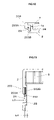
- FIG. 1 is a planar view diagram which shows the external appearance of an SD memory cardTM related to the first embodiment.
- FIG. 2 is a cross sectional view of the line A-A′ of the SD memory cardTM shown in FIG. 1 related to the first embodiment.
- FIG. 3 is a diagram which shows a cross section of a potting resin part shown in FIG. 2 relate to the first embodiment.
- FIG. 4 is a planar view diagram which shows the internal structure of a top case shown in FIG. 1 and FIG. 2 related to the first embodiment.
- FIG. 5 is a planar view diagram which shows the structure of an element mounting surface of the substrate 5 shown in FIG. 2 related to the first embodiment.
- FIG. 6 is a cross sectional view diagram which shows the structure of a write protect switch part shown in FIG. 1 related to the first embodiment.
- FIG. 7 is a planar view diagram which shows the structure of a write protect switch part shown in FIG. 1 related to the first embodiment.
- FIG. 8 is a cross sectional view diagram which shows the structure of the SD memory cardTM related to the first embodiment.
- FIG. 9 is a cross sectional view diagram which shows the structure of resin potting part shown in FIG. 8 related to the first embodiment.
- FIG. 10 is a planar view diagram which shows the structure of the substrate shown in FIG. 8 seen from the bottom surface, related to the first embodiment.
- FIG. 11 is a diagram which shows an example where warping occurs on a substrate due to the resin potting of a controller chip related to the first embodiment.
- FIG. 12 is a cross sectional view diagram which shows the structure of the write protect switch part related to the first embodiment.
- FIG. 13 is a planar view diagram which shows the structure of the write protect switch part related to the first embodiment.
- FIG. 14 is a planar view diagram which shows the structure of the interior of a bottom case attached to the top case shown in FIG. 12 and FIG. 13 related to the first embodiment.
- FIG. 15 is cross sectional view diagram which shows the structure of the SD cardTM related to the second embodiment.
- FIG. 16 is a planar view diagram which shows the structure of the substrate shown in FIG. 15 seen from the bottom surface, related to the second embodiment.
- FIG. 17 us a cross sectional view diagram which shows the structure of the structure of the SD cardTM related to the third embodiment.
- FIG. 18 is a planar view diagram which shows the structure of the substrate shown in FIG. 17 seen from the bottom surface, related to the third embodiment.
- FIG. 19 is cross sectional view diagram which shows another structure of the SD cardTM related to the third embodiment.
- FIG. 20 is a planar view diagram which shows the structure of the substrate shown in FIG. 19 seen from the bottom surface, related to the third embodiment.
- FIG. 21 is a diagram which shows an example structure of a solder resist pattern of the mounting surface of a memory package of the substrate related to another embodiment.
- FIG. 22 is a diagram which shows an example structure of a solder resist pattern of the mounting surface of a memory package of the controller chip related to another embodiment.
- FIG. 23 is a diagram which shows an example structure of a bonding pad of the controller chip related to another embodiment.
- FIG. 24 is a diagram which shows the manufacturing process of the SD memory cardTM related to another embodiment.
- FIG. 1 is a planar view diagram which shows the exterior appearance of an SD memory cardTM.
- the SD memory cardTM 100 includes a top case (first case element) 1 , a label sticker groove part 8 , a grip 9 and a write protect switch 17 .
- the vertical direction in the diagram indicates the insertion direction in which the SD memory cardTM which is connected to an external device is inserted.
- the label sticker groove part 8 is a part to which a label printed with the specifications etc of the SD memory cardTM 100 is attached.
- the grip 9 is a part which part which is held when the SD memory cardTM 100 is connected to or removed from an external device.
- the write protect switch 17 is a switch which operates when writing data to the memory package mounted with the SD memory cardTM 100 is forbidden.
- the write protect switch 17 can be switched between a write protect mode setting and release of a write protect mode by sliding the switch in the direction of the arrow shown in the diagram.
- FIG. 2 is a cross sectional view diagram of the line A-A′ of the SD memory cardTM shown in FIG. 1 .
- the same symbols are attached to the same structural elements shown in FIG. 1 .
- 2 is a bottom case (second case element)
- 3 is a memory package (semiconductor memory package) which uses a NAND type flash memory etc
- 4 is a resin potting
- 5 is a substrate
- 6 is a terminal part which for connecting with a terminal of an external device
- 7 is a terminal part case rib
- 10 is an top case rib.
- FIG. 3 is a diagram which shows a cross section of the resin potting 4 parts shown in FIG. 2 .
- TSOP Thin Small Outline Package
- LGA Land Grid Package
- BGA All Grid Array
- FIG. 4 is a planar view diagram which shows the structure within the top case 1 shown in FIG. 1 and FIG. 2 .
- 13 is a recess part which houses the write protect switch 17
- 14 is a protrusion part for welding (energy director) for welding the top case 1 to the bottom case 2 .
- the protrusion part for welding 14 is arranged around the entire edge part within the top case 1 .
- FIG. 5 is a planar view diagram which shows the structure of an element mounting surface of the substrate 5 shown in FIG. 2 .
- 15 is a test pad which is used when testing the operation of the memory package 3 and the controller chip 12
- 16 is a chip condenser.
- a recess part 13 is formed corresponding to the recess part 13 which is formed in a mounting position of the write protect switch 17 in the above stated bottom case 2 on the substrate 5 .
- FIG. 6 is a cross sectional view diagram which shows the structure of the write protect switch 17 part shown in FIG. 1 .
- FIG. 7 is planar view diagram which shows the structure of the write protect switch 17 part shown in FIG. 1 .
- the same symbols are used for the same structural elements as in FIG. 1 .
- the write protect switch 17 is comprised from an operation part 17 A in an operation direction shown in FIG. 1 , and a switch main body part 17 B which slides along the inner surface of the bottom case 2 according to an operation of the operation part 17 A.
- 18 is a protrusion part for switch operation and is arranged on a side surface within the bottom case 2 .
- the protrusion part for switch operation 18 is arranged so that resistance is provided to the switch main body part 17 B when sliding the operation part 17 A of the write protect switch 17 .
- the write protect switch 17 does not perform a slide operation unless a certain amount of force is applied to the operation part 17 A. That is, the protrusion part for switch operation 18 is arranged so that setting and release of a write protect mode can be operated reliably.
- the external dimensions of the SD memory cardTM 100 constructed as shown in FIG. 1 to FIG. 7 are regulated.
- the external dimensions of the external appearance view of the SD memory cardTM 100 shown in FIG. 1 are, for example, height 32 mm and length 24 mm.
- the thickness of the entire case constructed from the top case 1 and the bottom case 2 is 2.1 mm. Therefore, in the SD memory cardTM 100 , it is necessary to house the substrate 5 , the memory package 3 , the controller chip 12 , the chip condenser 16 and the write protect switch 17 etc within the external dimensions shown.
- the external dimensions of the SD memory cardTM 100 are regulated as stated above, the external dimensions of the substrate 5 which is housed in the case are also restricted and each external dimension of the memory package 3 and controller chip 12 which can be mounted on the substrate 5 are also restricted. Furthermore, because the recess part 13 is formed on the substrate 5 in order to secure a mounting region for the write protect switch 17 , the chip mounting region is further reduced. Therefore, as in the SD memory cardTM shown in FIG. 2 , in the construction where the memory package 3 and the controller chip 12 are mounted on only one surface of the substrate 5 , it is becoming increasingly difficult to realize a chip arrangement in which memory capacity within a limited mounting region on the substrate 5 , is further increased.
- FIG. 8 to FIG. 14 shown below an example structure is shown in which a plurality of memory packages can be mounted on the substrate 5 in the SD memory cardTM which has regulated dimensions.
- FIG. 8 is a cross sectional view diagram which shows a construction of a SD memory cardTM 200 related to the first embodiment.
- FIG. 9 is a cross section view diagram which shows a construction of a resin potting 4 part shown in FIG. 8 .
- FIG. 8 and FIG. 9 the same structural elements as in FIG. 2 and FIG. 3 have the same symbols.
- two memory packages 3 A and 3 B are mounted on the top surface (first surface) of a substrate 201 and the controller chip 12 sealed by the resin potting 4 is mounted on the bottom surface (second surface) of the substrate 201 .
- the controller chip 12 sealed by the resin potting 4 is mounted on the bottom surface (second surface) of the substrate 201 .
- the two memory packages 3 A and 3 B are mounted on the top surface of the substrate 201 . Therefore, in the SD memory cardTM 200 , by mounting two memory packages 3 A and 3 B which have the same memory capacity as the memory package 3 mounted in the SD memory cardTM 100 stated above, it is possible to easily increase memory capacity by at least twice.
- FIG. 10 is a planar view diagram which shows the construction of the substrate 201 shown in FIG. 8 , seen from the bottom surface.
- the controller chip 12 is mounted in a roughly central position of the bottom surface of the substrate 201 (middle position of the two memory packages 3 A, 3 B) according to the mounting position of the memory packages 3 A and 3 B.
- a plurality of chip condensers 16 are mounted in the upper part of the bottom surface of the substrate 201 . Setting of the mounting position of this controller chip 12 is determined by the following reasons.
- the mounting region of the memory packages 3 A and 3 B which are mounted on the top surface of the substrate 201 is expanded, the external dimensions of the write protect switch are reduced.
- the recess part formed on the substrate 201 corresponding to the mounting position of the write protect switch is also reduced. This structure will be explained while referring to FIG. 10 , and FIG. 12 to FIG. 14 .
- a recess part 202 is formed on the left side of the substrate 201 corresponding to a mounting position of the write protect switch.
- the dimension L 1 of this recess part 202 shown in FIG. 10 is smaller than the dimension L 1 of the recess part 13 shown in FIG. 5 .
- the dimension L 2 of the recess part 202 shown in FIG. 10 is the same as the dimension L 2 of the recess part 13 shown in FIG. 5 .
- the dimension L 1 of the recess part 202 is about 0.7 to 0.9 mm
- the dimension of L 1 of the recess part 13 is about 2 mm
- dimension of L 2 is about 15 mm. Because the dimension L 1 of the recess part 202 is reduced, an example of the reduced dimensions of each part related to the write protect switch 17 shown in FIG. 6 and FIG. 7 is shown in FIG. 12 and FIG. 13 .
- FIG. 12 us a cross sectional view diagram which shows the structure of the write protect switch 203 part.
- FIG. 13 is a planar view diagram which shows the structure of the write protect switch 203 part.
- the same symbols are used for the same structural elements shown in FIG. 6 and FIG. 7 .
- the write protect switch 203 includes an operation part 203 A and a switch main body 203 B the same as the write protect switch 17 shown in FIG. 6 and FIG. 7 .
- This write protect switch 203 uses the write protect switch main body 203 B shown in FIG. 13 with reduced dimensions.
- this write protect switch 203 it is possible to form the thickness L 3 of an external wall rib 2 A of the lower case 2 which houses the switch main body 203 B, thinner than the thickness L 3 of the external wall rib 2 A of the lower case 2 shown in FIG. 7 . Furthermore, the thickness of the external wall rib 2 A of the bottom case 2 which houses the switch main body 203 B is about 0.25 mm, and the thickness of the external wall rib 2 A of the lower case 2 which houses the switch main body 17 is about 0.5 mm.
- the distance L 4 from the external wall rib 2 A of the bottom case 2 which houses the switch main body 203 B shown in FIG. 13 , to the internal wall rib 2 B can similarly be further reduced when compared to the distance L 4 shown in FIG. 5 .
- the distance L 4 from the external wall rib 2 A which houses the write protect switch 203 to the internal wall rib 2 B is about 1.1 mm
- the distance L 4 from the external wall rib 2 A which houses the write protect switch 17 to the internal wall rib 2 B is about 2.4 mm.
- the write protect switch 203 is housed so that the operation part 203 A is not exposed to the exterior of the bottom case 2 from the recess part 202 when the write protect switch 203 is housed in a mounting region formed in the recess part 202 .
- the write protect switch 203 with reduced dimensions as above, it is possible to reduce the dimensions in a depth direction of the region in which the write protect switch 203 of the bottom case 2 is mounted. As a result, the dimension L 1 in a depth direction of the recess part 202 in the substrate 201 can be reduced and the region in which the memory packages 3 A and 3 B are mounted on the top surface of the substrate 201 can be expanded.
- a protrusion part for switch operation 204 is arranged on the bottom surface part between the external wall rib 2 A of the bottom case which houses the write protect switch 203 and the internal wall rib 2 B.
- the protrusion part for switch operation 204 is arranged so that the switch main body 203 is provided with resistance when sliding the operation part 203 A of the write protect switch 203 , similar to the protrusion part for switch operation 18 shown in FIG. 6 .
- the write protect switch 203 does not slide unless the operation part 203 A is applied with a certain amount of force (for example, about 1 to 4N). That is, the protrusion part for switch operation 204 is arranged so that setting and release of a write protect mode can be operated reliably.
- FIG. 14 is a planar view diagram which shows the internal structure of the top case 1 (first case) welded and the bottom case 2 (second case) shown in FIG. 12 and FIG. 13 .
- 202 is a recess part which houses the write protect switch 17
- 14 is protrusion part for welding (energy director) for welding the top case 1 and bottom case 2 .
- the protrusion part for welding 14 is arranged the entire edge part within the top case 1 .
- This protrusion part for welding 14 is formed with a reduced width the same size as the reduction in thickness of the inner wall rib 2 B shown in FIG. 12 .
- the SD memory cardTM 200 related to the first embodiment has a structure in which two memory packages (semiconductor chips) 3 A and 3 B are mounted on the top surface (first surface) of the substrate 201 and a controller chip 12 is mounted on the bottom surface (second surface) of the substrate 201 .
- the mounting position of the controller chip 12 is set in a roughly central position on the bottom surface of the substrate 201 (middle position of the two memory packages 3 A and 3 B), so that the effects of indentation shaped warping which occurs in the substrate 201 when the controller chip 12 is sealed by the resin potting 4 , are reduced. Therefore, in the SD memory cardTM 200 , it is possible to increase memory capacity by at least twice compared to when the memory package 3 and the controller chip 12 were mounted only on the top surface of the substrate.
- each dimension L 1 to L 4 of the bottom case 2 and top case 1 related to this mounting region can be reduced using the write protect switch 203 with reduced dimensions.
- the region in which the memory packages 3 A and 3 B are mounted on the top surface of the substrate 201 can be further expanded.
- FIG. 15 is a cross sectional view diagram which shows the structure of an SD memory cardTM 300 related to the second embodiment.
- FIG. 16 is a planar view diagram which shows the structure of the substrate 201 shown in FIG. 15 seen from the bottom surface. In FIG. 15 and FIG. 16 , the same symbols are used for the same structural elements shown in FIG. 8 and FIG. 10 .
- the structural elements which are different to those of the SD memory cardTM 200 shown in the first embodiment are that a resin 301 is coated to the top surface of the substrate 201 which is mounted with the memory packages 3 A and 3 B. This resin 301 is coated only to both side parts of the substrate 201 in a position between the two memory packages 3 A and 3 B.
- the resin 301 By coating the resin 301 in this way, it is possible to relax the transformation of the substrate 201 which bends when a bending force is applied to the SD memory cardTM 300 , and prevent cracks etc appearing in the controller chip 12 . That is, because the resin 301 is coated to a position in which bending force is concentrated, it is possible to reinforce the strength of the substrate 201 .
- FIG. 17 is a cross sectional view diagram which shows the structure of an SD memory cardTM 400 related to the third embodiment.
- FIG. 18 is a planar view diagram which shows the structure of the substrate 201 shown in FIG. 17 seen from the bottom surface. In FIG. 17 and FIG. 18 , the same symbols are used for the same structural elements shown in FIG. 8 and FIG. 10 .
- the structural elements which are different to those of the SD memory cardTM 200 shown in the first embodiment are that the mounting position of the controller chip 12 which is mounted on the bottom surface of the substrate 201 has been changed to directly below the memory package 3 B.
- the mounting position of the controller chip 12 which is mounted on the bottom surface of the substrate 201 may be changed to directly below the memory package 3 A.
- the length of a wire (not shown in the diagram) which connects the controller chip 12 and the terminal parts 6 can be shortened when compared to the mounting position of the controller chip 12 shown in FIG. 17 and FIG. 18 .
- the wire length between the controller chip 12 and the terminal parts 6 it becomes possible to increase the speed of transmission of a signal which is input to the controller chip 12 from the terminal parts 6 . As a result, this also contributes to improving the operation speed of the SD memory cardTM 400 .
- FIG. 21 is a diagram which shows an example structure of solder regist opening pattern of the memory package mounting surface on the substrate 201 .
- the same symbols are used for the same structural elements shown in FIG. 10 .
- a solder regist opening pattern 211 and 212 are formed to match each position of the solder connection terminals of the memory packages 3 A and 3 B on the mounting surface of the memory packages 3 A and 3 B on the substrate 201 .
- FIG. 22 is a diagram which shows an example structure of solder regist pattern of the controller chip mounting surface on the substrate 201 .
- the same symbols are used for the same structural elements shown in FIG. 10 .
- a pattern 231 which shows the mounting position of the controller chip 12 and solder regist opening patterns 232 to 234 are formed to match each pad position of the bonding pad of the controller chip 12 on the mounting surface of the controller chip 12 on the substrate 201 .
- gold terminal patterns 221 to 229 are formed corresponding to the pin positions of the terminals parts 6 shown in FIG. 2 , on the mounting surface of the controller chip 12 of the substrate 201 .
- the gold terminal pattern 221 corresponds to DAT 1 pin (8 th pin)
- the gold terminal pattern 222 corresponds to pin DAT 0 (7 th pin)
- the gold terminal pattern 223 corresponds to pin GND (6 th pin)
- the gold terminal pattern 224 corresponds to pin CLK (5 th pin)
- the gold terminal pattern 225 corresponds to pin Vcc (4 th pin)
- the gold terminal pattern 226 corresponds to pin GND (3 th pin)
- the gold terminal pattern 227 corresponds to pin CMD (2 nd pin)
- the gold terminal pattern 228 corresponds to pin DAT 3 (1 st pin)
- the gold terminal pattern 229 corresponds to pin DAT 2 (0 th pin).
- FIG. 23 is a diagram which shows an example structure of a bonding pad of the controller chip 12 .
- terminal groups 12 A to 12 C which connect the bonding wires are shown formed on the upper, lower and right sides of the diagram.
- Bonding pad groups 41 A to 41 C are formed to match the formation position of these terminal groups 12 A to 12 C.
- Each terminal group 12 A to 12 C and each bonding pad group 41 A to 41 C are connected by bonding wire groups 11 A to 11 C.
- the bonding pad groups 41 A and 41 B are arranged in an arch shape so that the distance of the bonding wire groups 11 A and 11 B are nearly the same.
- the difference between the length of the wires of the bonding wire groups 11 A and 11 B is about 30%.
- FIG. 24 is a diagram which shows an example of the manufacturing process of the SD memory cardsTM 200 , 300 and 400 shown in the first, second and third embodiments described above.
- the substrate is created (step S 101 ).
- a test pad 15 solder regist opening patterns 211 , 212 , a pattern 231 , gold terminal patterns 221 to 229 and solder regist opening patterns 232 to 234 are formed on the top and bottom surfaces of the substrate 201 .
- controller chip 12 is fixed to the bottom surface of the substrate 201 by die bonding (step S 102 ).
- each terminal group 12 A to 12 C and each bonding pad group 41 A to 41 C of the controller chip 12 are connected together by the wire bonding groups 11 A to 11 C by a wire bonding (step S 103 ).
- the controller chip 12 is sealed by a resin potting 4 (step S 104 ).
- step S 105 a solder paste is printed to the terminal parts which connect the memory packages 3 A, 3 B and the chip condensers 16 on the substrate 201
- step S 106 the memory packages 3 A and 3 B are mounted on the top surface of the substrate 201
- step S 10 chip condensers 16 are mounted in the mounting position of the condenser on the top surface of the substrate 201 (step S 10 ).
- step S 108 each terminal of the memory packages 3 A, 3 B and chip condensers 16 and the solder regist patterns 232 to 234 on the top surface of the substrate 201 are connected using solder by reflow
- step S 109 the resin 301 is coated to both side parts between the two memory packages 3 A and 3 B which are mounted on the top surface of the substrate 201 (step S 109 ). Furthermore, because this process is a process corresponding to the SD memory cardTM 300 shown in the second embodiment described above, this process can be omitted. Furthermore, in FIG. 24 , the step S 109 shown in the brackets, shows a process which can be omitted. The mounting process of the chip on the substrate or the elements on the chip is completed by the processes in the steps S 101 to S 109 .
- the substrate 201 is mounted in a substrate mounting position within the bottom case 2 (step S 110 ).
- the write protect switch 203 is mounted in a switch mounting position in the bottom case 2 (step S 111 ).
- the top case 1 is attached to the bottom case 2 (step S 112 ).
- the bottom case 2 and the top case 1 are joined by ultrasonic welding (step S 113 ). In this case, when an ultrasonic welding process is performed, the bottom case 2 and the top case 1 are welded and joined by the welding protrusion part (energy director) which is arranged around the entire inner side of the top case 1 .
- the memory cards 200 , 300 and 400 shown in the first, second and third embodiments are completed by the manufacturing process described above.
- the first, second and third embodiments described above showed the case where an SD memory cardTM was used, however, the embodiments are not limited to an SD memory cardTM.
- the present invention can also be applied to other semiconductor memory cards as long as an external case includes the regulated dimensions, such as a mini SD cardTM.
Abstract
Description
Claims (15)
Applications Claiming Priority (2)
| Application Number | Priority Date | Filing Date | Title |
|---|---|---|---|
| JP2007334782A JP2009157628A (en) | 2007-12-26 | 2007-12-26 | Semiconductor memory card |
| JP2007-334782 | 2007-12-26 |
Publications (2)
| Publication Number | Publication Date |
|---|---|
| US20090168322A1 US20090168322A1 (en) | 2009-07-02 |
| US8097939B2 true US8097939B2 (en) | 2012-01-17 |
Family
ID=40798038
Family Applications (1)
| Application Number | Title | Priority Date | Filing Date |
|---|---|---|---|
| US12/334,642 Expired - Fee Related US8097939B2 (en) | 2007-12-26 | 2008-12-15 | Semiconductor memory card |
Country Status (4)
| Country | Link |
|---|---|
| US (1) | US8097939B2 (en) |
| JP (1) | JP2009157628A (en) |
| KR (1) | KR20090071460A (en) |
| TW (1) | TWI389040B (en) |
Cited By (18)
| Publication number | Priority date | Publication date | Assignee | Title |
|---|---|---|---|---|
| USD734755S1 (en) * | 2013-06-26 | 2015-07-21 | Samsung Electronics Co., Ltd. | Solid state drive |
| USD734756S1 (en) * | 2014-04-04 | 2015-07-21 | Pny Technologies, Inc. | Reduced length memory card |
| USD735204S1 (en) * | 2013-06-26 | 2015-07-28 | Samsung Electronics Co., Ltd. | Solid state drive |
| USD735203S1 (en) * | 2013-06-26 | 2015-07-28 | Samsung Electronics Co., Ltd. | Solid state drive |
| USD735202S1 (en) * | 2013-06-26 | 2015-07-28 | Samsung Electronics Co., Ltd. | Solid state drive |
| USD736213S1 (en) * | 2014-07-01 | 2015-08-11 | Samsung Electronics Co., Ltd. | Memory card |
| USD736216S1 (en) * | 2014-07-30 | 2015-08-11 | Samsung Electronics Co., Ltd. | Memory card |
| USD739856S1 (en) * | 2014-07-30 | 2015-09-29 | Samsung Electronics Co., Ltd. | Memory card |
| US20150380062A1 (en) * | 2009-08-28 | 2015-12-31 | Kabushiki Kaisha Toshiba | Memory module and video camera |
| US9286951B2 (en) | 2012-04-30 | 2016-03-15 | Kabushiki Kaisha Toshiba | Memory card and SD card |
| US9442539B2 (en) | 2013-04-05 | 2016-09-13 | Pny Technologies, Inc. | Reduced length memory card |
| US9569717B2 (en) | 2014-06-10 | 2017-02-14 | Kabushiki Kaisha Toshiba | Memory card |
| USD780184S1 (en) * | 2013-03-13 | 2017-02-28 | Nagrastar Llc | Smart card interface |
| USD780763S1 (en) * | 2015-03-20 | 2017-03-07 | Nagrastar Llc | Smart card interface |
| USD791772S1 (en) * | 2015-05-20 | 2017-07-11 | Chaya Coleena Hendrick | Smart card with a fingerprint sensor |
| US10070176B2 (en) | 2013-03-13 | 2018-09-04 | Nagrastar, Llc | Systems and methods for performing transport I/O |
| USD840404S1 (en) * | 2013-03-13 | 2019-02-12 | Nagrastar, Llc | Smart card interface |
| USD864968S1 (en) * | 2015-04-30 | 2019-10-29 | Echostar Technologies L.L.C. | Smart card interface |
Families Citing this family (19)
| Publication number | Priority date | Publication date | Assignee | Title |
|---|---|---|---|---|
| US8472199B2 (en) * | 2008-11-13 | 2013-06-25 | Mosaid Technologies Incorporated | System including a plurality of encapsulated semiconductor chips |
| JP2010160647A (en) * | 2009-01-07 | 2010-07-22 | Toshiba Corp | Semiconductor memory card |
| USD759022S1 (en) * | 2013-03-13 | 2016-06-14 | Nagrastar Llc | Smart card interface |
| US20150254545A1 (en) * | 2014-03-10 | 2015-09-10 | Kabushiki Kaisha Toshiba | Memory card |
| USD730908S1 (en) * | 2014-05-02 | 2015-06-02 | Samsung Electronics Co., Ltd. | Memory card |
| USD730910S1 (en) * | 2014-05-02 | 2015-06-02 | Samsung Electronics Co., Ltd. | Memory card |
| USD730907S1 (en) * | 2014-05-02 | 2015-06-02 | Samsung Electronics Co., Ltd. | Memory card |
| USD727912S1 (en) * | 2014-06-27 | 2015-04-28 | Samsung Electronics Co., Ltd. | Memory card |
| USD729251S1 (en) * | 2014-06-27 | 2015-05-12 | Samsung Electronics Co., Ltd. | Memory card |
| USD727911S1 (en) * | 2014-06-27 | 2015-04-28 | Samsung Electronics Co., Ltd. | Memory card |
| USD730909S1 (en) * | 2014-06-27 | 2015-06-02 | Samsung Electronics Co., Ltd. | Memory card |
| USD727913S1 (en) * | 2014-06-27 | 2015-04-28 | Samsung Electronics Co., Ltd. | Memory card |
| USD736215S1 (en) * | 2014-07-01 | 2015-08-11 | Samsung Electronics Co., Ltd. | Memory card |
| USD736212S1 (en) * | 2014-07-01 | 2015-08-11 | Samsung Electronics Co., Ltd. | Memory card |
| USD736214S1 (en) * | 2014-07-01 | 2015-08-11 | Samsung Electronics Co., Ltd. | Memory card |
| USD727910S1 (en) * | 2014-07-02 | 2015-04-28 | Samsung Electronics Co., Ltd. | Memory card |
| JP6253607B2 (en) * | 2015-03-16 | 2017-12-27 | 東芝メモリ株式会社 | Manufacturing method of semiconductor memory card |
| USD783621S1 (en) * | 2015-08-25 | 2017-04-11 | Samsung Electronics Co., Ltd. | Memory card |
| USD783622S1 (en) * | 2015-08-25 | 2017-04-11 | Samsung Electronics Co., Ltd. | Memory card |
Citations (6)
| Publication number | Priority date | Publication date | Assignee | Title |
|---|---|---|---|---|
| US6590778B1 (en) * | 1999-08-06 | 2003-07-08 | Matsushita Electric Industrial Co., Ltd. | Memory card |
| US20030183914A1 (en) * | 2002-03-28 | 2003-10-02 | Wallace Robert F. | Improved memory package with a controller on one side of a printed circuited board and memory on another side of the circuit board |
| WO2004081858A1 (en) | 2003-03-10 | 2004-09-23 | Matsushita Electric Works Ltd. | Adaptor for memory card |
| JP2007128959A (en) | 2005-11-01 | 2007-05-24 | Toshiba Corp | Semiconductor memory card and circuit board |
| US20070228509A1 (en) | 2006-03-31 | 2007-10-04 | Kabushiki Kaisha Toshiba | Semiconductor device and memory card using the same |
| US20070263365A1 (en) * | 2004-06-18 | 2007-11-15 | Hiroyuki Yamada | Ic Card |
Family Cites Families (3)
| Publication number | Priority date | Publication date | Assignee | Title |
|---|---|---|---|---|
| JPH03129244U (en) * | 1990-04-06 | 1991-12-25 | ||
| JP2002015296A (en) * | 2000-06-30 | 2002-01-18 | Matsushita Electric Ind Co Ltd | Memory card |
| JP2006313432A (en) * | 2005-05-06 | 2006-11-16 | Matsushita Electric Ind Co Ltd | Control circuit board and memory card |
-
2007
- 2007-12-26 JP JP2007334782A patent/JP2009157628A/en active Pending
-
2008
- 2008-12-15 US US12/334,642 patent/US8097939B2/en not_active Expired - Fee Related
- 2008-12-17 TW TW097149167A patent/TWI389040B/en not_active IP Right Cessation
- 2008-12-24 KR KR1020080133698A patent/KR20090071460A/en not_active Application Discontinuation
Patent Citations (7)
| Publication number | Priority date | Publication date | Assignee | Title |
|---|---|---|---|---|
| US6590778B1 (en) * | 1999-08-06 | 2003-07-08 | Matsushita Electric Industrial Co., Ltd. | Memory card |
| US20030183914A1 (en) * | 2002-03-28 | 2003-10-02 | Wallace Robert F. | Improved memory package with a controller on one side of a printed circuited board and memory on another side of the circuit board |
| WO2004081858A1 (en) | 2003-03-10 | 2004-09-23 | Matsushita Electric Works Ltd. | Adaptor for memory card |
| US20060014434A1 (en) | 2003-03-10 | 2006-01-19 | Toshihiro Yamamoto | Adaptor for memory card |
| US20070263365A1 (en) * | 2004-06-18 | 2007-11-15 | Hiroyuki Yamada | Ic Card |
| JP2007128959A (en) | 2005-11-01 | 2007-05-24 | Toshiba Corp | Semiconductor memory card and circuit board |
| US20070228509A1 (en) | 2006-03-31 | 2007-10-04 | Kabushiki Kaisha Toshiba | Semiconductor device and memory card using the same |
Non-Patent Citations (2)
| Title |
|---|
| Office Action issued Jun. 20, 2011 in Korean Application No. 10-2008-133698 (w/partial English translation). |
| U.S. Appl. No. 12/610,504, filed Nov. 2, 2009, Okada. |
Cited By (19)
| Publication number | Priority date | Publication date | Assignee | Title |
|---|---|---|---|---|
| US20150380062A1 (en) * | 2009-08-28 | 2015-12-31 | Kabushiki Kaisha Toshiba | Memory module and video camera |
| US9286951B2 (en) | 2012-04-30 | 2016-03-15 | Kabushiki Kaisha Toshiba | Memory card and SD card |
| USD780184S1 (en) * | 2013-03-13 | 2017-02-28 | Nagrastar Llc | Smart card interface |
| US10382816B2 (en) | 2013-03-13 | 2019-08-13 | Nagrastar, Llc | Systems and methods for performing transport I/O |
| USD840404S1 (en) * | 2013-03-13 | 2019-02-12 | Nagrastar, Llc | Smart card interface |
| US10070176B2 (en) | 2013-03-13 | 2018-09-04 | Nagrastar, Llc | Systems and methods for performing transport I/O |
| US9442539B2 (en) | 2013-04-05 | 2016-09-13 | Pny Technologies, Inc. | Reduced length memory card |
| USD734755S1 (en) * | 2013-06-26 | 2015-07-21 | Samsung Electronics Co., Ltd. | Solid state drive |
| USD735202S1 (en) * | 2013-06-26 | 2015-07-28 | Samsung Electronics Co., Ltd. | Solid state drive |
| USD735204S1 (en) * | 2013-06-26 | 2015-07-28 | Samsung Electronics Co., Ltd. | Solid state drive |
| USD735203S1 (en) * | 2013-06-26 | 2015-07-28 | Samsung Electronics Co., Ltd. | Solid state drive |
| USD734756S1 (en) * | 2014-04-04 | 2015-07-21 | Pny Technologies, Inc. | Reduced length memory card |
| US9569717B2 (en) | 2014-06-10 | 2017-02-14 | Kabushiki Kaisha Toshiba | Memory card |
| USD736213S1 (en) * | 2014-07-01 | 2015-08-11 | Samsung Electronics Co., Ltd. | Memory card |
| USD739856S1 (en) * | 2014-07-30 | 2015-09-29 | Samsung Electronics Co., Ltd. | Memory card |
| USD736216S1 (en) * | 2014-07-30 | 2015-08-11 | Samsung Electronics Co., Ltd. | Memory card |
| USD780763S1 (en) * | 2015-03-20 | 2017-03-07 | Nagrastar Llc | Smart card interface |
| USD864968S1 (en) * | 2015-04-30 | 2019-10-29 | Echostar Technologies L.L.C. | Smart card interface |
| USD791772S1 (en) * | 2015-05-20 | 2017-07-11 | Chaya Coleena Hendrick | Smart card with a fingerprint sensor |
Also Published As
| Publication number | Publication date |
|---|---|
| KR20090071460A (en) | 2009-07-01 |
| TWI389040B (en) | 2013-03-11 |
| JP2009157628A (en) | 2009-07-16 |
| TW200947314A (en) | 2009-11-16 |
| US20090168322A1 (en) | 2009-07-02 |
Similar Documents
| Publication | Publication Date | Title |
|---|---|---|
| US8097939B2 (en) | Semiconductor memory card | |
| KR100472334B1 (en) | Wiring board, semiconductor device and method of producing, testing and packaging the same, and circuit board and electronic equipment | |
| US8754534B2 (en) | Semiconductor device | |
| US7939927B2 (en) | Semiconductor memory apparatus | |
| US7981788B2 (en) | Semiconductor device and a manufacturing method of the same | |
| US7378726B2 (en) | Stacked packages with interconnecting pins | |
| US7608787B2 (en) | Semiconductor memory device and USB memory device using the same | |
| US20100187690A1 (en) | Semiconductor device | |
| JP2010160647A (en) | Semiconductor memory card | |
| US20090179318A1 (en) | Multi-channel stackable semiconductor device and method for fabricating the same, and stacking substrate applied to the semiconductor device | |
| US6242285B1 (en) | Stacked package of semiconductor package units via direct connection between leads and stacking method therefor | |
| JP5166903B2 (en) | Semiconductor device | |
| JP6454656B2 (en) | USB device and manufacturing method thereof | |
| US20100210042A1 (en) | Method of manufacturing semiconductor module | |
| US20090323294A1 (en) | Memory card and method of manufacturing the same | |
| KR200251183Y1 (en) | Ultra-Thin Stack Package Device and Ultra-Thin Memory Card Employing Such Package Device | |
| JP3707987B2 (en) | Semiconductor device and module mounted with the semiconductor device | |
| US20230154835A1 (en) | Semiconductor package including connection pad including groove pattern | |
| JP2007193763A (en) | Semiconductor memory card | |
| KR100543900B1 (en) | Multi-layer-type semiconductor package and method for manufacturing the same | |
| JP6706994B2 (en) | Substrate, semiconductor module, and method for manufacturing semiconductor module | |
| JP5834108B2 (en) | Semiconductor device | |
| KR200281137Y1 (en) | Multi-layer-type semiconductor package using saw-tooth-type connection pcb | |
| JP2001188888A (en) | Non-contact type ic card and method for manufacturing the same | |
| KR20050043057A (en) | A stack package and it's manufacture method |
Legal Events
| Date | Code | Title | Description |
|---|---|---|---|
| AS | Assignment |
Owner name: KABUSHIKI KAISHA TOSHIBA, JAPAN Free format text: ASSIGNMENT OF ASSIGNORS INTEREST;ASSIGNOR:OKADA, TAKASHI;REEL/FRAME:022230/0170 Effective date: 20090116 |
|
| ZAAA | Notice of allowance and fees due |
Free format text: ORIGINAL CODE: NOA |
|
| ZAAB | Notice of allowance mailed |
Free format text: ORIGINAL CODE: MN/=. |
|
| STCF | Information on status: patent grant |
Free format text: PATENTED CASE |
|
| FEPP | Fee payment procedure |
Free format text: PAYOR NUMBER ASSIGNED (ORIGINAL EVENT CODE: ASPN); ENTITY STATUS OF PATENT OWNER: LARGE ENTITY |
|
| FPAY | Fee payment |
Year of fee payment: 4 |
|
| AS | Assignment |
Owner name: TOSHIBA MEMORY CORPORATION, JAPAN Free format text: ASSIGNMENT OF ASSIGNORS INTEREST;ASSIGNOR:KABUSHIKI KAISHA TOSHIBA;REEL/FRAME:043709/0035 Effective date: 20170706 |
|
| MAFP | Maintenance fee payment |
Free format text: PAYMENT OF MAINTENANCE FEE, 8TH YEAR, LARGE ENTITY (ORIGINAL EVENT CODE: M1552); ENTITY STATUS OF PATENT OWNER: LARGE ENTITY Year of fee payment: 8 |
|
| FEPP | Fee payment procedure |
Free format text: MAINTENANCE FEE REMINDER MAILED (ORIGINAL EVENT CODE: REM.); ENTITY STATUS OF PATENT OWNER: LARGE ENTITY |
|
| LAPS | Lapse for failure to pay maintenance fees |
Free format text: PATENT EXPIRED FOR FAILURE TO PAY MAINTENANCE FEES (ORIGINAL EVENT CODE: EXP.); ENTITY STATUS OF PATENT OWNER: LARGE ENTITY |
|
| STCH | Information on status: patent discontinuation |
Free format text: PATENT EXPIRED DUE TO NONPAYMENT OF MAINTENANCE FEES UNDER 37 CFR 1.362 |
|
| FP | Lapsed due to failure to pay maintenance fee |
Effective date: 20240117 |