US8045052B2 - Image processing device and associated operating method - Google Patents
Image processing device and associated operating method Download PDFInfo
- Publication number
- US8045052B2 US8045052B2 US11/574,458 US57445805A US8045052B2 US 8045052 B2 US8045052 B2 US 8045052B2 US 57445805 A US57445805 A US 57445805A US 8045052 B2 US8045052 B2 US 8045052B2
- Authority
- US
- United States
- Prior art keywords
- image
- signal
- processing device
- image processing
- input signals
- Prior art date
- Legal status (The legal status is an assumption and is not a legal conclusion. Google has not performed a legal analysis and makes no representation as to the accuracy of the status listed.)
- Expired - Fee Related, expires
Links
- 238000012545 processing Methods 0.000 title claims abstract description 101
- 238000011017 operating method Methods 0.000 title claims abstract description 11
- 230000001360 synchronised effect Effects 0.000 claims description 14
- 230000008859 change Effects 0.000 claims description 5
- 238000000034 method Methods 0.000 claims description 5
- 230000008569 process Effects 0.000 claims description 5
- 230000010363 phase shift Effects 0.000 claims description 3
- 230000001960 triggered effect Effects 0.000 claims description 3
- 238000012937 correction Methods 0.000 description 12
- GJWAPAVRQYYSTK-UHFFFAOYSA-N [(dimethyl-$l^{3}-silanyl)amino]-dimethylsilicon Chemical compound C[Si](C)N[Si](C)C GJWAPAVRQYYSTK-UHFFFAOYSA-N 0.000 description 9
- 238000010586 diagram Methods 0.000 description 8
- XUIMIQQOPSSXEZ-UHFFFAOYSA-N Silicon Chemical compound [Si] XUIMIQQOPSSXEZ-UHFFFAOYSA-N 0.000 description 2
- 230000001588 bifunctional effect Effects 0.000 description 2
- 238000012986 modification Methods 0.000 description 2
- 230000004048 modification Effects 0.000 description 2
- 239000004926 polymethyl methacrylate Substances 0.000 description 2
- 229910052710 silicon Inorganic materials 0.000 description 2
- 239000010703 silicon Substances 0.000 description 2
- 238000012800 visualization Methods 0.000 description 2
- 239000003086 colorant Substances 0.000 description 1
- 230000000295 complement effect Effects 0.000 description 1
- 230000001419 dependent effect Effects 0.000 description 1
- 238000011161 development Methods 0.000 description 1
- 230000018109 developmental process Effects 0.000 description 1
- 230000006870 function Effects 0.000 description 1
- 238000002156 mixing Methods 0.000 description 1
- 230000003287 optical effect Effects 0.000 description 1
- 238000009877 rendering Methods 0.000 description 1
Images


Classifications
-
- H—ELECTRICITY
- H04—ELECTRIC COMMUNICATION TECHNIQUE
- H04N—PICTORIAL COMMUNICATION, e.g. TELEVISION
- H04N5/00—Details of television systems
- H04N5/04—Synchronising
- H04N5/06—Generation of synchronising signals
- H04N5/067—Arrangements or circuits at the transmitter end
- H04N5/073—Arrangements or circuits at the transmitter end for mutually locking plural sources of synchronising signals, e.g. studios or relay stations
- H04N5/0736—Arrangements or circuits at the transmitter end for mutually locking plural sources of synchronising signals, e.g. studios or relay stations using digital storage buffer techniques
-
- H—ELECTRICITY
- H04—ELECTRIC COMMUNICATION TECHNIQUE
- H04N—PICTORIAL COMMUNICATION, e.g. TELEVISION
- H04N5/00—Details of television systems
- H04N5/222—Studio circuitry; Studio devices; Studio equipment
- H04N5/262—Studio circuits, e.g. for mixing, switching-over, change of character of image, other special effects ; Cameras specially adapted for the electronic generation of special effects
- H04N5/2624—Studio circuits, e.g. for mixing, switching-over, change of character of image, other special effects ; Cameras specially adapted for the electronic generation of special effects for obtaining an image which is composed of whole input images, e.g. splitscreen
-
- H—ELECTRICITY
- H04—ELECTRIC COMMUNICATION TECHNIQUE
- H04N—PICTORIAL COMMUNICATION, e.g. TELEVISION
- H04N9/00—Details of colour television systems
- H04N9/12—Picture reproducers
- H04N9/31—Projection devices for colour picture display, e.g. using electronic spatial light modulators [ESLM]
- H04N9/3141—Constructional details thereof
- H04N9/3147—Multi-projection systems
Definitions
- the invention relates to an image processing device and to an associated operating method.
- one disadvantage of the known graphics systems for combining different graphics signals is the fact that they receive synchronized graphics signals on the input side.
- the graphics signals to be combined with one another are often asynchronous, which makes it more difficult to combine them using the known graphics systems or requires specially synchronized graphics systems.
- FIG. 8.71 discloses an image processing device, which can receive different, unsynchronized image input signals on the input side and only then synchronizes them, whereupon the synchronized image input signals are then combined by means of a combiner to form an image output signal.
- This known image processing device therefore advantageously makes it possible to combine unsynchronized image input signals.
- one disadvantage with the above-described known image processing devices is the unsatisfactory image quality when a plurality of unsynchronized image input signals are combined with one another and then geometrically distorted or rectified.
- the task of the invention is therefore to provide an image processing device and an associated operating method which gives an improved image quality when combining a plurality of image input signals and carrying out geometric distortion or rectification.
- the invention comprises an image processing device comprising a plurality of image signal inputs for receiving a respective image input signal, wherein the individual image input signals usually represent an image or a sequence of images.
- the invention is not restricted to a specific number of image signal inputs, but the image processing device according to the invention preferably has eight image signal inputs so that a total of eight different image input signals can be received.
- the invention can also be implemented with a different number of image signal inputs, for example with two, four, six or more image signal inputs.
- the image processing device preferably has at least one image signal output for outputting an image output signal, wherein the image output signal usually represents an image or a sequence of images.
- the invention is also not restricted to a single image signal output. Rather, it is also possible to provide a plurality of image signal outputs so as to output a corresponding number of image output signals.
- the individual image output signals may in this case represent different images or sequences of images.
- the different image signal outputs output image output signals in different data formats, wherein the different image output signals may then represent the same image or the same sequence of images. It is, e.g., possible that one image signal output outputs a digital image output signal, whereas another image signal output of the image processing device according to the invention outputs an analogue image output signal.
- the image processing device preferably comprises a combiner for combining the different image input signals with one another to form the image output signal or to form the individual image output signals.
- the image processing device makes it possible to receive unsynchronized image input signals, so that a synchronizer is respectively connected downstream of the individual image signal inputs, which synchronizer synchronizes the unsynchronized image input signals for the subsequent combining operation.
- the combiner of the image processing device preferably includes a programmable or configurable combinational circuit, which combines the different image input signals with one another in accordance with predefined (preferably variable) programming to form the image output signal and which can be programmed or configured via a serial and/or parallel programming interface.
- the combining of the different image input signals can therefore be set at the pixel level by means of corresponding programming of the programmable combinational circuit, so that any combinations of the image input signals received on the input side are possible.
- the programmable combinational circuit for combining the different image input signals preferably has an FPGA (Field Programmable Gate Array), but it is in principle also possible that the combiner in the image processing device according to the invention has a PLD (Programmable Logic Device) or a PAL (Programmable Array Logic).
- FPGA Field Programmable Gate Array
- PLD Programmable Logic Device
- PAL Programmable Array Logic
- an FPGA available from the company XILINX may be used as the combiner, although the invention is not restricted to this type of FPGA as combiner. Nevertheless, the use of FPGAs of the Virtex II Pro X or Virtex IV type from the company XILINX is particularly advantageous.
- the combiner of the image processing device according to the invention is preferably connected to a random access memory, the content of which defines the combination of the image input signals.
- a random access memory the content of which defines the combination of the image input signals.
- This may be for example a DDR-RAM which may have for example a storage capacity of 128 MBit.
- the combiner is connected to a read-only memory which contains a start configuration for the combiner, wherein the start configuration is loaded into the combiner at the time of switch-on.
- This read-only memory may be for example a JTAG Flash memory, but the invention is not restricted to this type of memory with regard to the type of memory for the read-only memory for storing the start configuration.
- the image processing device has at least one signal splitter which is connected on the input side to at least one of the image signal inputs and on the output side to at least two of the synchronizers, wherein the signal splitter splits the image input signal applied on the input side between the synchronizers connected to the signal splitter on the output side.
- This splitting of an image input signal between a plurality of synchronizers may be useful in order to circumvent bandwidth limitations of the synchronizers and to process image input signals with very high bandwidth requirements, as a plurality of synchronizers jointly synchronize and distort one image input signal, wherein the synchronized subsignals are then appropriately recombined by the combiner.
- the signal splitter receives a respective image input signal on the input side and splits it between two synchronizers, where said signal is synchronized and corrected.
- the invention is not restricted to a splitting ratio of 1:2 but rather can also be implemented with other splitting ratios, for example a splitting ratio of 1:3, 1:4 or more, if the bandwidth limitation of the synchronizers and the bandwidth of the image input signals make this necessary.
- the signal splitters can preferably be programmed so as, depending on the programming, either to feed each image input signal to a respective one of the synchronizers or to split the individual image input signals in each case between a plurality of the synchronizers.
- the image processing device according to the invention therefore has at least two operating modes, wherein the signal splitters are inactive in one operating mode and are switched to the active state in another operating mode in order to split the respective individual image input signals between a plurality of the synchronizers.
- a signal splitter is connected downstream of respective pairs of individual image signal inputs, wherein the individual signal splitters can preferably be programmed individually. It is then possible that one signal splitter of the image processing device according to the invention is switched to the inactive state while another signal splitter of the image processing device according to the invention is switched to the active state.
- the image processing device preferably comprises a central clock generator which is connected on the output side to all the synchronizers. This makes it possible for the individual image input signals to be synchronized by the individual synchronizers independently of their frequency and resolution, so that the signals provided at the outputs of the synchronizers are synchronized down to pixel level.
- the image processing device may further comprise an external synchronization terminal for synchronizing the image processing device with other image processing devices.
- the image processing device further includes at least one distorter or rectifier for respectively individually distorting or rectifying the individual image input signals before they are combined to form the image output signal.
- the distorter or rectifier is formed by the individual synchronizers, which therefore have two functions, namely on the one hand the synchronization of the image input signals and on the other hand the distortion or rectification thereof.
- This is provided for example by the chip type sxT1 from the company Silicon Optix, which also has the name “Reon”.
- the invention is not restricted to chips of this type but rather can also in principle be implemented with other types of chip.
- the synchronizers are preferably bifunctional in that they allow not only the synchronization of the input signals but also the distortion or rectification thereof.
- the modules referred to as synchronizers within the context of this description may also be referred to as correction modules due to the fact that they are bifunctional, wherein the correction modules or synchronizers offer the following advantages.
- each correction module or synchronizer can correct different resolutions or clock rates of the image signal inputs, so that a uniform image signal is output at the output of each correction module or synchronizer and is passed on to the combiner.
- the individual correction modules or synchronizers can correct the respective image signal individually with regard to geometry and/or brightness and/or color.
- the individual correction modules or synchronizers can individually chop and change the size of (enlarge and reduce) the respective image signal, as a result of which just part of the respective image signal is passed on to the combiner.
- distaltion or rectification of image signals which is used within the context of the invention is therefore meant in the geometrical sense and not in the telecommunications sense and encompasses, in addition to the geometric correction of the image content, also the correction of the brightness and of the color information.
- the individual synchronizers preferably in each case have a control input, via which a change of image can be triggered, wherein the control inputs of the individual synchronizers are preferably jointly connected to the combiner in order to receive a common trigger signal from the combiner.
- This joint triggering of the individual synchronizers by the combiner permits a synchronous change of image, which is usually a prerequisite for the subsequent combining operation.
- the individual synchronizers can preferably be configured via a respective configuration input, wherein the individual configuration inputs of the synchronizers are connected to the combiner via a multiplexer.
- the combiner can in this case address and configure all the synchronizers via the multiplexer.
- the image signal output of the image processing device may be connected to an image display device, such as a projector or a monitor for example.
- One advantageous field of application of the image processing device according to the invention consists in the split image calculation in a plurality of nodes of a graphics cluster, if the calculation capacity of the individual nodes alone is not sufficient.
- the image calculation is split between a plurality of graphics computers such that each processes just part of the image.
- the coordination of this parallel image calculation may be carried out for example by a control computer.
- the subsignals processed by the individual graphics computers are then fed to the image signal inputs of the image processing device according to the invention, synchronized and subsequently recombined.
- the invention also comprises an operating method for an image processing device according to the invention, as is already clear from the above description.
- FIG. 1 shows a simplified block diagram of an image processing device according to the invention for combining eight image input signals to form four image output signals
- FIG. 2 shows the signal splitter of the image processing device of FIG. 1 ,
- FIG. 3 shows a more detailed block diagram of part of the image processing device of FIG. 1 .
- FIG. 4 shows a graphics system according to the invention comprising a graphics cluster for the parallel processing of graphics signals
- FIG. 5 shows a graphics system for projecting image signals
- FIG. 6 shows a simplified block diagram of an image processing system according to the invention comprising a plurality of graphics computers as image signal sources and the image processing device according to the invention for combining these image input signals, and
- FIGS. 7A , 7 B show a timing diagram which illustrates the rough synchronization of the image input signals in the graphics computers of the image processing system shown in FIG. 6 .
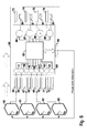
- FIG. 1 shows an example of embodiment of an image processing device 1 according to the invention for combining eight unsynchronized image input signals Video In 1 , . . . , Video In 8 to form four image output signals Video Out 1 , . . . , Video Out 4 .
- the image processing device 1 In order to receive the individual unsynchronized image input signals Video In 1 , . . . , Video In 8 , the image processing device 1 has a plurality of digital input interfaces 2 - 9 (DVI-D: Digital Video Interface).
- DVI-D Digital Video Interface
- the individual pixel information items are in each case transmitted in the form of an 8-bit value, wherein the image value for the primary colors red, yellow and blue are transmitted in parallel for each pixel.
- the individual input interfaces 2 - 9 are in each case connected in pairs on the output side to a plurality of signal splitters 10 - 13 , the structure of which is shown in more detail in FIG. 2 and will be described in more detail below.
- the individual signal splitters 10 - 13 are connected to eight synchronizers 14 - 21 , which in each case receive two image signals from the individual signal splitters 10 - 13 and synchronize said signals.
- the synchronizers 14 - 21 are chips of the type sxT1 from the company Silicon Optix, which are also referred to as “Reon”.
- the image signals synchronized by the synchronizers 14 - 21 are then fed to a combiner 22 , which is an FPGA (Field Programmable Gate Array) of the type Virtex-II from the company XILINX.
- the combiner 22 combines the image signals received on the input side in accordance with predefined programming (not shown here) to form the image output signals Video Out 1 , . . . , Video Out 4 , and outputs these signals at a plurality of output interfaces 23 - 26 .
- the image processing device 1 further has a parallel interface 27 and a serial interface 28 for configuring the image processing device 1 .
- the image processing device 1 also has a central clock generator 29 which is connected on the output side to the synchronizers 14 - 21 .
- This common clocking of the individual synchronizers 14 - 21 makes it possible for the image input signals Video In 1 , . . . , Video In 8 to be synchronized independently of their frequency and resolution, so that the signals provided at the outputs of the synchronizers 14 - 21 are synchronized down to pixel level.
- the combiner 22 is connected to the individual synchronizers 14 - 21 via a multiplexer 30 , so as to configure the synchronizers individually.
- the combiner 22 is connected to the individual signal splitters 10 - 13 in order to be able to switch them between two operating modes.
- the signal splitters 10 - 13 are inactive, so that the two respective image input signals applied on the input side are switched through to the associated synchronizers.
- the signal splitters 10 - 13 are switched to the active state, so that only the image input signal applied to one of the two signal inputs is split between the two synchronizers connected on the output side.
- this operating mode it is also possible to process image input signals having a bandwidth greater than the maximum processing bandwidth of the synchronizers 14 - 21 .
- the signal splitter 10 On the input side, the signal splitter 10 has two TMDS receivers 31 , 32 which are connected on the input side to the two input interfaces 2 , 3 and generate an RGB signal having a width of 48 bits.
- the TMDS receiver 32 in one of the two parallel branches can be switched to the inactive state by the combiner 22 via a control line 33 and an inverter 34 , so that the TMDS receiver 32 does not output an image signal.
- An amplifier 35 is moreover arranged between the two signal processing branches, which amplifier can pass the image signal output by the TMDS receiver 31 to the synchronizer 15 of the other signal processing branch.
- the amplifier 35 can in this case also be switched to the inactive state by the combiner 22 via the control line 33 , the inverter 34 and a further inverter 36 .
- the two inverters 34 , 36 thus ensure that either the TMDS receiver 32 or the amplifier 35 is switched to the active state.
- This splitting of the image input signals received on the input side makes it possible to circumvent bandwidth limitations of the synchronizers 14 - 21 and to process image input signals of higher bandwidth.
- each input interface 2 , 3 has a respective DDC-EEPROM 37 , 38 which provides a DDC string.
- each of the synchronizers 14 , 15 is connected to a random access memory 39 , 40 , in which the image data are buffer-stored.
- the combiner 22 is also connected to a memory 41 , in which the start configuration for the combiner 22 is stored, wherein the start configuration is loaded into the combiner 22 from the memory 41 at the time of switch-on.
- the memory 41 is a JTAG Flash memory.
- a plurality of graphics computers 44 - 47 calculates respective image sections of a high-resolution image.
- a control computer 43 carries out the coordination of the image calculation on the individual graphics computers 44 - 47 . Due to the fact that the image signal to be processed is split in this way between a plurality of graphics computers 44 - 47 , it is possible to achieve a high processing capacity using simple graphics computers.
- the individual graphics computers 44 - 47 are connected to an image processing device 48 according to the invention, which synchronizes and combines the unsynchronized output signals of the individual graphics computers 44 - 47 so that a combined image output signal Video Out is provided at the output of the image processing device 48 .
- FIG. 5 the example of embodiment of a graphics system according to the invention which is shown in FIG. 5 will be described, in which two image input signals Video In 1 , Video In 2 are fed to an image processing device 51 according to the invention, which geometrically distorts the image input signals Video In 1 , Video In 2 in order to compensate the curvature of a projection surface 52 , and also corrects the brightness and color so as to compensate any differences between the projectors 53 , 54 .
- the image processing device 51 is connected to two projectors 53 , 54 , which project the two image output signals Video Out 1 , Video Out 2 onto the projection surface 52 .
- the two images projected by the projectors 53 and 54 overlap in an overlap area 55 on the projection surface 52 .
- the image processing device makes it possible to carry out a brightness correction for the image signals in this area, which permits so-called “edge blending”.
- FIG. 6 shows a simplified block diagram of an image processing system according to the invention comprising a plurality of graphics computers 60 , 61 , 62 , 63 which each supply an image input signal, wherein the image input signals provided by the graphics computers 60 - 63 are unsynchronized.
- the illustrated image processing system has an image processing device 64 according to the invention comprising a plurality of image signal inputs 65 - 72 and a plurality of image signal outputs 73 - 76 .
- the image signal inputs 65 - 72 are supplied with the unsynchronized image input signals from the graphics computers 60 - 63 .
- a respective so-called WARP chip 77 - 84 is connected downstream of the individual image signal inputs 65 - 72 in the image processing device 64 , wherein said chip is in each case essentially a synchronizer which synchronizes the unsynchronized image input signals received on the input side with one another.
- the WARP chips 77 - 84 are connected to a combiner 85 in the form of an FPGA.
- the combiner 85 is in turn connected on the output side to the image signal outputs 73 - 76 via a plurality of TMDS transmitters 86 - 89 .
- the image processing device 64 in this example of embodiment also has a plurality of analogue output interfaces 90 - 93 .
- the phase difference between the image input signals received from the graphics computers 60 - 63 is determined in the image processing device 64 and coupled back to the graphics computers 60 - 63 via an interface 94 .
- the graphics computers 60 - 63 then carry out rough synchronization of the image input signals fed into the image processing device 64 , so that the image processing device 64 then has to perform only fine synchronization of the image input signals.
- the image processing device 64 has a possibility for synchronization which can synchronize the image signals down to the pixel level (“GENLOCK”), so that the image input signals received via the image signal inputs 65 - 72 need not be provided in a synchronous manner down to the pixel level.
- the image input signals are provided in a manner such that they are already roughly synchronized.
- the only important thing here is that the time of the respective image start (“FRAMESYNC”) is phase-shifted by no more than 5-10° relative to the other image input signals (“FRAMELOCK”).
- the exact synchronization of the image input signals (“GENLOCK”) is then carried out by the WARP chips 77 - 84 of the image processing device 64 .
- the rough synchronization of the image input signals fed into the image processing device 64 may be implemented in the graphics computers 60 - 63 by a software routine which increases or reduces the length of the vertical blanking interval of the image signals, as can be seen from the timing diagrams in FIGS. 7A and 7B . All that is required for this is the information concerning the actual phase shift of the image input signals, which is provided by the image processing device 64 via the interface 94 .
Abstract
Description
-
- Shawky, M.; Bonnet, S.; Favad, S.; Crubille, P.: “A Computing Platform and its Tools for Feature Extraction from On-Vehicle Image Sequences”, IEEE Intelligent Transportation Systems Conference, 2000, Dearborn, Mich., USA, 1-3 Oct. 2000, Conference Proceedings, pp. 39-45.
- DE 103 14 105 A1
- DD 228 136 A1
- LYNX Technik AG: “Series 3000 MiniModules. Product Catalog”, company publication, S3000MM Ver 1.0., Weiterstadt: LYNX, 2003
- LI, Kai; CHEN, Han; CHEN, Yuqun et al.: “Building and Using a Scalable Display Wall System”, IEEE Computer Graphics and Applications, Vol. 20, No. 4, July/August 2000, pp. 29-37.
- ALLARD, Jeremie; GOURANTON, Valerie; LECOINTRE, Loick et al.: “Neff Juggler and SoftGenLock: Running VR Juggler with Active Stereo and Multiple Displays on a Commodity Computer Cluster”, IEEE Virtual Reality Conference 2002, VR'02, Orlando, Fla., USA, 24-28 Mar. 2002.
- 1 image processing device
- 2-9 input interfaces
- 10-13 signal splitters
- 14-21 synchronizers
- 22 combiner
- 23-26 output interfaces
- 27 parallel interface
- 28 serial interface
- 29 clock generator
- 30 multiplexer
- 31 TMDS receiver
- 32 TMDS receiver
- 33 control line
- 34 inverter
- 35 amplifier
- 36 inverter
- 37 DDC-EEPROM
- 38 DDC-EEPROM
- 39 random access memory
- 40 random access memory
- 41 memory
- 42 --
- 43 control computer
- 44-47 graphics computers
- 48 image processing device
- 49 projector
- 50 projection surface
- 51 image processing device
- 52 projection surface
- 53 projector
- 54 projector
- 60-63 graphics computers
- 64 image processing device
- 65-72 image signal inputs
- 73-76 image signal outputs
- 77-84 WARP chips
- 85 combiner
- 86-89 TMDS transmitters
- 90-93 analogue interfaces
- 94 interface
- VIDEO IN 1, . . . ,
- VIDEO IN 8 video input signals
- VIDEO OUT 1, . . . ,
- VIDEO OUT 4 video output signals
-
Video 1, . . . , -
Video 4 video signals
Claims (25)
Applications Claiming Priority (4)
| Application Number | Priority Date | Filing Date | Title |
|---|---|---|---|
| DE102004042166 | 2004-08-31 | ||
| DE102004042166.8 | 2004-08-31 | ||
| DE102004042166A DE102004042166A1 (en) | 2004-08-31 | 2004-08-31 | Image processing device and corresponding operating method |
| PCT/EP2005/054282 WO2006024646A1 (en) | 2004-08-31 | 2005-08-31 | Image processing device and associated operating method |
Publications (2)
| Publication Number | Publication Date |
|---|---|
| US20090040394A1 US20090040394A1 (en) | 2009-02-12 |
| US8045052B2 true US8045052B2 (en) | 2011-10-25 |
Family
ID=35169538
Family Applications (1)
| Application Number | Title | Priority Date | Filing Date |
|---|---|---|---|
| US11/574,458 Expired - Fee Related US8045052B2 (en) | 2004-08-31 | 2005-08-31 | Image processing device and associated operating method |
Country Status (4)
| Country | Link |
|---|---|
| US (1) | US8045052B2 (en) |
| EP (1) | EP1784975A1 (en) |
| DE (1) | DE102004042166A1 (en) |
| WO (1) | WO2006024646A1 (en) |
Families Citing this family (3)
| Publication number | Priority date | Publication date | Assignee | Title |
|---|---|---|---|---|
| US7986217B2 (en) * | 2007-09-27 | 2011-07-26 | Intel Corporation | Mitigating processing latency in RFID exchanges |
| TWI457877B (en) * | 2010-01-07 | 2014-10-21 | Univ Nat Taipei Technology | Display wall system and high-resolution graphics and images generation and display method |
| US20130324874A1 (en) * | 2012-06-01 | 2013-12-05 | Xerox Corporation | Minute ventilation estimation based on chest volume |
Citations (17)
| Publication number | Priority date | Publication date | Assignee | Title |
|---|---|---|---|---|
| DD228136A1 (en) | 1982-09-23 | 1985-10-02 | Post Rundfunk U Fernsehtechnis | CIRCUIT ARRANGEMENT FOR GENERATING A MIXED VIDEO SIGNAL |
| US5057910A (en) * | 1987-02-20 | 1991-10-15 | Magni Systems, Inc. | Method of displaying video signal phase characteristics |
| US5136390A (en) | 1990-11-05 | 1992-08-04 | Metavision Corporation | Adjustable multiple image display smoothing method and apparatus |
| US5499375A (en) * | 1993-06-03 | 1996-03-12 | Texas Instruments Incorporated | Feedback register configuration for a synchronous vector processor employing delayed and non-delayed algorithms |
| US5550594A (en) * | 1993-07-26 | 1996-08-27 | Pixel Instruments Corp. | Apparatus and method for synchronizing asynchronous signals |
| US5760729A (en) * | 1995-05-01 | 1998-06-02 | Thomson Consumer Electronics, Inc. | Flash analog-to-digital converter comparator reference arrangement |
| US20020015055A1 (en) * | 2000-07-18 | 2002-02-07 | Silicon Graphics, Inc. | Method and system for presenting three-dimensional computer graphics images using multiple graphics processing units |
| US6456737B1 (en) * | 1997-04-15 | 2002-09-24 | Interval Research Corporation | Data processing system and method |
| WO2002104009A1 (en) | 2001-06-19 | 2002-12-27 | Ecole Polytechnique Federale De Lausanne (Epfl) | Method and system for combining video with spatio-temporal alignment |
| US20030038807A1 (en) | 2001-08-22 | 2003-02-27 | Demos Gary Alfred | Method and apparatus for providing computer-compatible fully synchronized audio/video information |
| US20030149987A1 (en) | 2002-02-06 | 2003-08-07 | Pasqualino Christopher R. | Synchronization of data links in a multiple link receiver |
| US20030179740A1 (en) | 2000-10-23 | 2003-09-25 | Jamal Baina | Method for synchronizing digital signals |
| US20030222987A1 (en) * | 2002-05-30 | 2003-12-04 | Karazuba Paul M. | Line scan image recording device with internal system for delaying signals from multiple photosensor arrays |
| DE10314105A1 (en) | 2003-03-28 | 2004-01-08 | Bts Media Solutions Gmbh | Method for controlling a device for distributing and processing video signals |
| EP1427197A1 (en) | 2002-12-03 | 2004-06-09 | Ming-Ho Yu | Apparatus for producing TV advertising contents and inserting interstitial advertisements on TV programs |
| US20040131276A1 (en) * | 2002-12-23 | 2004-07-08 | John Hudson | Region-based image processor |
| US7167191B2 (en) * | 1999-11-17 | 2007-01-23 | Ricoh Company, Ltd. | Techniques for capturing information during multimedia presentations |
Family Cites Families (3)
| Publication number | Priority date | Publication date | Assignee | Title |
|---|---|---|---|---|
| US6469741B2 (en) * | 1993-07-26 | 2002-10-22 | Pixel Instruments Corp. | Apparatus and method for processing television signals |
| US6340991B1 (en) * | 1998-12-31 | 2002-01-22 | At&T Corporation | Frame synchronization in a multi-camera system |
| US6507370B1 (en) * | 2000-03-20 | 2003-01-14 | International Business Machines Corporation | Highly adjustable video composite sync separator and variable gain pixel clock frequency locking apparatus and method |
-
2004
- 2004-08-31 DE DE102004042166A patent/DE102004042166A1/en not_active Withdrawn
-
2005
- 2005-08-31 WO PCT/EP2005/054282 patent/WO2006024646A1/en active Application Filing
- 2005-08-31 US US11/574,458 patent/US8045052B2/en not_active Expired - Fee Related
- 2005-08-31 EP EP05779122A patent/EP1784975A1/en not_active Ceased
Patent Citations (19)
| Publication number | Priority date | Publication date | Assignee | Title |
|---|---|---|---|---|
| DD228136A1 (en) | 1982-09-23 | 1985-10-02 | Post Rundfunk U Fernsehtechnis | CIRCUIT ARRANGEMENT FOR GENERATING A MIXED VIDEO SIGNAL |
| US5057910A (en) * | 1987-02-20 | 1991-10-15 | Magni Systems, Inc. | Method of displaying video signal phase characteristics |
| US5136390A (en) | 1990-11-05 | 1992-08-04 | Metavision Corporation | Adjustable multiple image display smoothing method and apparatus |
| US5499375A (en) * | 1993-06-03 | 1996-03-12 | Texas Instruments Incorporated | Feedback register configuration for a synchronous vector processor employing delayed and non-delayed algorithms |
| US5550594A (en) * | 1993-07-26 | 1996-08-27 | Pixel Instruments Corp. | Apparatus and method for synchronizing asynchronous signals |
| US5760729A (en) * | 1995-05-01 | 1998-06-02 | Thomson Consumer Electronics, Inc. | Flash analog-to-digital converter comparator reference arrangement |
| US6456737B1 (en) * | 1997-04-15 | 2002-09-24 | Interval Research Corporation | Data processing system and method |
| US7167191B2 (en) * | 1999-11-17 | 2007-01-23 | Ricoh Company, Ltd. | Techniques for capturing information during multimedia presentations |
| US20020015055A1 (en) * | 2000-07-18 | 2002-02-07 | Silicon Graphics, Inc. | Method and system for presenting three-dimensional computer graphics images using multiple graphics processing units |
| US20030179740A1 (en) | 2000-10-23 | 2003-09-25 | Jamal Baina | Method for synchronizing digital signals |
| WO2002104009A1 (en) | 2001-06-19 | 2002-12-27 | Ecole Polytechnique Federale De Lausanne (Epfl) | Method and system for combining video with spatio-temporal alignment |
| US20030038807A1 (en) | 2001-08-22 | 2003-02-27 | Demos Gary Alfred | Method and apparatus for providing computer-compatible fully synchronized audio/video information |
| US20030149987A1 (en) | 2002-02-06 | 2003-08-07 | Pasqualino Christopher R. | Synchronization of data links in a multiple link receiver |
| US20030222987A1 (en) * | 2002-05-30 | 2003-12-04 | Karazuba Paul M. | Line scan image recording device with internal system for delaying signals from multiple photosensor arrays |
| EP1427197A1 (en) | 2002-12-03 | 2004-06-09 | Ming-Ho Yu | Apparatus for producing TV advertising contents and inserting interstitial advertisements on TV programs |
| US20040131276A1 (en) * | 2002-12-23 | 2004-07-08 | John Hudson | Region-based image processor |
| WO2004057529A2 (en) | 2002-12-23 | 2004-07-08 | Gennum Corporation | Region-based image processor |
| DE10314105A1 (en) | 2003-03-28 | 2004-01-08 | Bts Media Solutions Gmbh | Method for controlling a device for distributing and processing video signals |
| US20040252241A1 (en) | 2003-03-28 | 2004-12-16 | Arnd Paulsen | Method for controlling a device for the distribution and processing of video signals |
Non-Patent Citations (9)
| Title |
|---|
| Allard et al., "Net Juggler and SoftGenLock: Running VR Juggler with Active Sterio and Multiple Displays on a Commodity Component Cluster", IEEE Computer Society (2002). |
| Anonymous, "Ausbildunghshandbuch audiovisuelle Medienberufe" pp. 344-411 (2003). |
| Colin, "Anyplace Projection", Projector Central (May 4, 2004). |
| International Search Report for PCT/EP2005/054282. |
| Li et al., "Building and Using a Scalable Display Wall System", IEEE Computer Graphics and Applications, pp. 29-37 (2000). |
| LYNX Technik AG, "Series 3000 MiniModules Product Catalog", pp. 1-11 (2003). |
| Meyer-Schwarzenberger, "Lexikon Video-, Audio-, und Netztechnik", p. 117 (2004). |
| Schmidt, "Professionelle Videotechnik", pp. 428-505 (2000). |
| Shawky et al., "A Computing Platform and its Tools for Features Extraction from On-Vehicle Image Sequences", IEEE Intelligent Transportation Systems, pp. 39-45 (2000). |
Also Published As
| Publication number | Publication date |
|---|---|
| DE102004042166A1 (en) | 2006-03-16 |
| WO2006024646A1 (en) | 2006-03-09 |
| EP1784975A1 (en) | 2007-05-16 |
| US20090040394A1 (en) | 2009-02-12 |
Similar Documents
| Publication | Publication Date | Title |
|---|---|---|
| US5488431A (en) | Video data formatter for a multi-channel digital television system without overlap | |
| US5497197A (en) | System and method for packaging data into video processor | |
| CA2241457A1 (en) | High definition television for simultaneously displaying plural images contained in broadcasting signals of mutually different broadcasting systems | |
| US8045052B2 (en) | Image processing device and associated operating method | |
| US7555021B2 (en) | Digital multi-source multi-destination video multiplexer and crossbar device | |
| US5673204A (en) | Loopback video preview for a computer display | |
| GB2371161A (en) | Synchronising a plurality of independent video signal generators | |
| EP1051026A2 (en) | Quad mode Cmos camera image sensor | |
| CA2309605C (en) | System and methods for 2-tap/3-tap flicker filtering | |
| KR19990060491A (en) | DTV's video display clock and sync signal generator | |
| US20060012613A1 (en) | Image processing device and image processing method | |
| JPH0215780A (en) | Apparatus and method for determining component picture element modulation data | |
| US7321403B2 (en) | Video signal transmitting/receiving system | |
| EP1164787A2 (en) | Video transmission apparatus | |
| WO2001003066A1 (en) | Apparatus and method for merging pixels | |
| US7301580B2 (en) | Method of realizing combination of multi-sets of multiple digital images and bus interface technique | |
| US6701027B1 (en) | Device for separating large images captured by data acquisition | |
| US20090180024A1 (en) | Image processing apparatus and image processing method | |
| KR0150965B1 (en) | The signal process circuit of wide tv | |
| JPH07154680A (en) | Video display device, screen display system using it, multi-pattern display system and magnification printed circuit board inserted to video display device main body | |
| JP2522193B2 (en) | Horizontal sync signal converter | |
| EP0651581B1 (en) | Improvements in video data formatters | |
| JPH11155101A (en) | Image compositing circuit | |
| JP2021078019A (en) | Image generation system, transmission device, transmission method, and program | |
| JP2000184315A (en) | Display unit and multi-screen display device |
Legal Events
| Date | Code | Title | Description |
|---|---|---|---|
| AS | Assignment |
Owner name: MAX-PLANCK-GESELLSCHAFT ZUR FOERDERUNG DER WISSENS Free format text: ASSIGNMENT OF ASSIGNORS INTEREST;ASSIGNORS:NUSSECK, HANS-GUENTHER;BUELTHOFF, HEINRICH H.;REEL/FRAME:019145/0067 Effective date: 20070327 |
|
| ZAAA | Notice of allowance and fees due |
Free format text: ORIGINAL CODE: NOA |
|
| ZAAB | Notice of allowance mailed |
Free format text: ORIGINAL CODE: MN/=. |
|
| STCF | Information on status: patent grant |
Free format text: PATENTED CASE |
|
| FPAY | Fee payment |
Year of fee payment: 4 |
|
| FEPP | Fee payment procedure |
Free format text: MAINTENANCE FEE REMINDER MAILED (ORIGINAL EVENT CODE: REM.); ENTITY STATUS OF PATENT OWNER: SMALL ENTITY |
|
| FEPP | Fee payment procedure |
Free format text: ENTITY STATUS SET TO UNDISCOUNTED (ORIGINAL EVENT CODE: BIG.); ENTITY STATUS OF PATENT OWNER: LARGE ENTITY |
|
| FEPP | Fee payment procedure |
Free format text: 7.5 YR SURCHARGE - LATE PMT W/IN 6 MO, LARGE ENTITY (ORIGINAL EVENT CODE: M1555); ENTITY STATUS OF PATENT OWNER: LARGE ENTITY |
|
| MAFP | Maintenance fee payment |
Free format text: PAYMENT OF MAINTENANCE FEE, 8TH YEAR, LARGE ENTITY (ORIGINAL EVENT CODE: M1552); ENTITY STATUS OF PATENT OWNER: LARGE ENTITY Year of fee payment: 8 |
|
| FEPP | Fee payment procedure |
Free format text: MAINTENANCE FEE REMINDER MAILED (ORIGINAL EVENT CODE: REM.); ENTITY STATUS OF PATENT OWNER: LARGE ENTITY |
|
| LAPS | Lapse for failure to pay maintenance fees |
Free format text: PATENT EXPIRED FOR FAILURE TO PAY MAINTENANCE FEES (ORIGINAL EVENT CODE: EXP.); ENTITY STATUS OF PATENT OWNER: LARGE ENTITY |
|
| STCH | Information on status: patent discontinuation |
Free format text: PATENT EXPIRED DUE TO NONPAYMENT OF MAINTENANCE FEES UNDER 37 CFR 1.362 |
|
| FP | Lapsed due to failure to pay maintenance fee |
Effective date: 20231025 |