US8039366B2 - Method for providing rotationally symmetric alignment marks for an alignment system that requires asymmetric geometric layout - Google Patents
Method for providing rotationally symmetric alignment marks for an alignment system that requires asymmetric geometric layout Download PDFInfo
- Publication number
- US8039366B2 US8039366B2 US12/388,851 US38885109A US8039366B2 US 8039366 B2 US8039366 B2 US 8039366B2 US 38885109 A US38885109 A US 38885109A US 8039366 B2 US8039366 B2 US 8039366B2
- Authority
- US
- United States
- Prior art keywords
- coded region
- coded
- alignment mark
- region
- gap
- Prior art date
- Legal status (The legal status is an assumption and is not a legal conclusion. Google has not performed a legal analysis and makes no representation as to the accuracy of the status listed.)
- Expired - Fee Related, expires
Links
Images


Classifications
-
- H—ELECTRICITY
- H01—ELECTRIC ELEMENTS
- H01L—SEMICONDUCTOR DEVICES NOT COVERED BY CLASS H10
- H01L21/00—Processes or apparatus adapted for the manufacture or treatment of semiconductor or solid state devices or of parts thereof
- H01L21/67—Apparatus specially adapted for handling semiconductor or electric solid state devices during manufacture or treatment thereof; Apparatus specially adapted for handling wafers during manufacture or treatment of semiconductor or electric solid state devices or components ; Apparatus not specifically provided for elsewhere
- H01L21/67005—Apparatus not specifically provided for elsewhere
- H01L21/67242—Apparatus for monitoring, sorting or marking
- H01L21/67294—Apparatus for monitoring, sorting or marking using identification means, e.g. labels on substrates or labels on containers
-
- H—ELECTRICITY
- H01—ELECTRIC ELEMENTS
- H01L—SEMICONDUCTOR DEVICES NOT COVERED BY CLASS H10
- H01L21/00—Processes or apparatus adapted for the manufacture or treatment of semiconductor or solid state devices or of parts thereof
- H01L21/67—Apparatus specially adapted for handling semiconductor or electric solid state devices during manufacture or treatment thereof; Apparatus specially adapted for handling wafers during manufacture or treatment of semiconductor or electric solid state devices or components ; Apparatus not specifically provided for elsewhere
- H01L21/68—Apparatus specially adapted for handling semiconductor or electric solid state devices during manufacture or treatment thereof; Apparatus specially adapted for handling wafers during manufacture or treatment of semiconductor or electric solid state devices or components ; Apparatus not specifically provided for elsewhere for positioning, orientation or alignment
- H01L21/681—Apparatus specially adapted for handling semiconductor or electric solid state devices during manufacture or treatment thereof; Apparatus specially adapted for handling wafers during manufacture or treatment of semiconductor or electric solid state devices or components ; Apparatus not specifically provided for elsewhere for positioning, orientation or alignment using optical controlling means
-
- H—ELECTRICITY
- H01—ELECTRIC ELEMENTS
- H01L—SEMICONDUCTOR DEVICES NOT COVERED BY CLASS H10
- H01L23/00—Details of semiconductor or other solid state devices
- H01L23/544—Marks applied to semiconductor devices or parts, e.g. registration marks, alignment structures, wafer maps
-
- H—ELECTRICITY
- H01—ELECTRIC ELEMENTS
- H01L—SEMICONDUCTOR DEVICES NOT COVERED BY CLASS H10
- H01L2223/00—Details relating to semiconductor or other solid state devices covered by the group H01L23/00
- H01L2223/544—Marks applied to semiconductor devices or parts
- H01L2223/54413—Marks applied to semiconductor devices or parts comprising digital information, e.g. bar codes, data matrix
-
- H—ELECTRICITY
- H01—ELECTRIC ELEMENTS
- H01L—SEMICONDUCTOR DEVICES NOT COVERED BY CLASS H10
- H01L2223/00—Details relating to semiconductor or other solid state devices covered by the group H01L23/00
- H01L2223/544—Marks applied to semiconductor devices or parts
- H01L2223/54426—Marks applied to semiconductor devices or parts for alignment
-
- H—ELECTRICITY
- H01—ELECTRIC ELEMENTS
- H01L—SEMICONDUCTOR DEVICES NOT COVERED BY CLASS H10
- H01L2223/00—Details relating to semiconductor or other solid state devices covered by the group H01L23/00
- H01L2223/544—Marks applied to semiconductor devices or parts
- H01L2223/54473—Marks applied to semiconductor devices or parts for use after dicing
- H01L2223/5448—Located on chip prior to dicing and remaining on chip after dicing
-
- H—ELECTRICITY
- H01—ELECTRIC ELEMENTS
- H01L—SEMICONDUCTOR DEVICES NOT COVERED BY CLASS H10
- H01L2924/00—Indexing scheme for arrangements or methods for connecting or disconnecting semiconductor or solid-state bodies as covered by H01L24/00
- H01L2924/0001—Technical content checked by a classifier
- H01L2924/0002—Not covered by any one of groups H01L24/00, H01L24/00 and H01L2224/00
Definitions
- the present invention generally relates to a method and apparatus of alignment marks on a semiconductor wafer that allow the alignment marks to be used when the semiconductor wafer or alignment marks are rotated 180 degrees from its expected orientation.
- Some solutions to this problem have been to buy new masks with properly placed alignment marks or to drop in additional alignment marks of a second mask. Problems with these known solutions are that new masks can be very costly ($100K or more in some cases) and dropping alignment marks off a second reticle can degrade the overall overlay performance by increasing the number of overlay error sources.
- the solution to this problem should address both of these deficiencies and provide a significant cost improvement rather than fixing and/or reordering new masks.
- the solution should provide that there is no degradation in overlay performance.
- the solution can not only address yield issues, but can also prevent devices from being defective.
- the exemplary aspects of the present invention provide an integrated circuit device, and at least one alignment mark on the integrated circuit device.
- the alignment mark comprises a first coded region, a second coded region adjacent the first coded region, and a third coded region adjacent the second coded region.
- the second coded region located (positioned) between the first coded region and the third coded region. Markings on the first coded region and the third coded region are identical.
- Another exemplary aspect of the present invention includes an integrated circuit device, and at least one alignment mark on the integrated circuit device.
- the alignment mark comprises a first coded region, a second coded region adjacent the first coded region, and a third coded region adjacent the second coded region.
- the second coded region located (positioned) between the first coded region and the third coded region. Markings on the first coded region and the third coded region are identical and at a different pitch than the second coded region.
- the first, second and third coded regions are generally aligned along a common linear direction, but do not need to be.
- the first, second and third coded regions can comprise a barcode, a glyph, and/or a computer readable graphic marking, etc.
- the first gap between the first coded region and the second coded region can be equal in dimension to a second gap between the second coded region and the third coded region.
- the geometric center of data for the alignment mark can be at the midpoint in the second coded region.
- the alignment mark can be symmetric about a line intersecting the midpoint and orthogonal to a common linear direction of the alignment mark.
- One method herein includes supplying an integrated circuit device and placing at least one alignment mark on the integrated circuit device.
- the alignment mark comprises a first coded region, a second coded region adjacent the first coded region, and a third coded region adjacent the second coded region.
- the second coded region located between the first coded region and the third coded region.
- the first coded region and the third coded region are identical.
- Another method herein includes supplying an integrated circuit device and placing at least one alignment mark on the integrated circuit device.
- the alignment mark comprises a first coded region, a second coded region adjacent the first coded region, and a third coded region adjacent the second coded region.
- the second coded region located between the first coded region and the third coded region.
- the markings on the first coded region and the third coded region being a different pitch than the second coded region.
- Another method herein includes aligning the first, second and third coded regions along a common linear direction.
- Another method herein includes the first, second and third coded regions further include one from the group of a barcode, a glyph, and/or a computer readable graphic marking.
- Another method herein includes leaving a first gap between the first coded region and the second coded region, and leaving a second gap between the second coded region and the third coded region, the first gap is equal in dimension to the second gap.
- Another method herein includes aligning a geometric center of data for the alignment mark at a midpoint of the second coded region. The alignment mark is symmetric about a line intersecting the midpoint and orthogonal to a common linear direction of the at least one alignment mark.
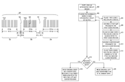
- FIG. 1 illustrates a schematic diagram of a wafer
- FIG. 2 illustrates a schematic diagram of alignment markings
- FIG. 3 a illustrates a schematic diagram of alignment markings
- FIG. 3 b illustrates a schematic diagram where the alignment mark of FIG. 3 is rotated 180 degrees
- FIG. 4 illustrates a flow-chart logic diagram of a method of an exemplary embodiment herein.
- FIGS. 1-4 there are shown exemplary embodiments of the method and apparatus of the present invention.
- CMOS complementary metal-oxide-semiconductor
- CMOS complementary metal-oxide-semiconductor
- a vendor for example, ASMLTM
- ASMLTM supplies designs of alignment marks compatible with their semiconductor fabricating equipment.
- These alignment marks are not rotationally symmetric but are asymmetrical in layout. For example, one end of a mark has 16.0 ⁇ m period and the other end of the mark has a 17.6 ⁇ m period.
- alignment marks are able to be placed where they are rotated by 180 degrees. This improper orientation causes the marks to be unreadable by manufacturing equipment and, therefore, they fail to work.
- Embodiments herein provide a single alignment mark that is overall symmetric so that if it is accidentally placed 180 degrees out of the expected orientation, the alignment mark is still useful.
- the mark of the present invention is designed in such a manner that a subsection of the printed pattern can be used for alignment in an asymmetric manner and still satisfy the requirements of the asymmetric alignment system.
- FIG. 1 illustrates a wafer 102 having a plurality of dies 104 wherein each die 104 is separated from adjacent dies by horizontal scribe lines 106 and vertical scribe lines 108 . At least one, (as shown in FIG. 1 ), horizontal small scribe line primary mark 110 a , and/or vertical small scribe line primary mark 110 b is placed near the scribe lines ( 106 and/or 108 ) to allow for intra-die alignment correction. Each die 104 may comprise at least one integrated circuit device.
- FIG. 2 illustrates an asymmetric alignment mark 200 .
- the 17.6 ⁇ m period section 202 is replicated on the left side of the mark, and a 16.0 ⁇ m period section 204 is replicated on the right side of the mark.
- the center of the mark 206 for alignment purposes is indicated by the plus “+” symbol, whereas the center of the data 208 is indicated by a diamond “ ⁇ ” symbol. If the data were to be rotated about the center of the data 208 , the layout of the mark 200 at the alignment position would be inverted, and therefore, unreadable.
- FIG. 3 a illustrates a symmetric alignment mark 300 .
- a 17.6 ⁇ m period section 302 is replicated (positioned) on the left side of the mark, and a center 16.0 ⁇ m period section 304 is replicated (positioned) to the right of left section 302 in the same manner as described above in FIG. 2 .
- a third 17.6 ⁇ m period section 306 is replicated to the right of section center section 304 and on the right side of the mark 300 .
- Section 306 is identical in data and form to the left section 302 .
- the center of the mark 308 for alignment purposes is indicated by the plus “+” symbol when the alignment mark 300 is (positioned) in a first orientation.
- the center of the data 310 is now (positioned) in a midpoint of the center section 304 .
- FIG. 3 b illustrates when the mark 300 of FIG. 3 a is rotated about the center of the data 310 as illustrated by the counter-clockwise direction arrow 314 .
- the layout of the mark 300 of FIG. 3 b at the alignment position would remain the same when the third section 306 is now located on the opposite side the mark, i.e., in FIG. 3 b , now on the left side of the mark 300 as compared with being located on the right side of the mark 300 as illustrated in FIG. 3 a.
- This ability of the present invention to rotate about the center of data and be readable in both orientations is unlike the standard ASML mark 200 of FIG. 2 that cannot be read when rotated about the center of data/mark 206 / 208 .
- the new center of the mark 312 for alignment purposes is indicated by the plus “+” symbol when the alignment mark 300 is (positioned) in a second orientation 180 degrees from the first orientation illustrated in FIG. 3 a.
- the apparatus of the present invention includes an integrated circuit device 104 , and at least one alignment mark 300 on the integrated circuit device 104 .
- the alignment mark 300 comprises a first coded region 302 , a second coded region 304 adjacent the first coded region 302 , and a third coded region 306 adjacent the second coded region 304 .
- the second coded region 304 located between the first coded region 302 and the third coded region 304 . Markings on the first coded region 304 and the third coded region 306 being identical.
- Markings on the first coded region 302 and the third coded region 306 are identical and at a different pitch (a 17.6 ⁇ m period section) than the second coded region 304 (a 16.0 ⁇ m period section).
- the first 302 , second 304 and third 306 coded regions are generally aligned along a common linear direction and can comprise a barcode, a glyph, and/or computer readable graphic markings.
- a first gap between the first coded region 302 and the second coded region 304 can be equal in dimension to a second gap between the second coded region 304 and the third coded region 306 .
- each gap is exemplarily illustrated to be 56.6 ⁇ m in length (28.6 ⁇ m+28.0 ⁇ m).
- a geometric center of data 310 for the alignment mark 300 is at a midpoint in the second coded region 304 , where the alignment mark 300 is symmetric about a line intersecting the midpoint and orthogonal to a common linear direction of the at least one alignment mark 300 .
- a method herein is illustrated in FIG. 4 includes supplying 400 an integrated circuit device, (e.g., on a wafer 102 of FIG. 1 on a specific die 104 ), and placing at least one alignment mark 300 on the integrated circuit device 402 .
- Placing the alignment mark 402 includes, (see FIGS. 3 a - 3 b ), placing 404 a first coded region 302 of the alignment mark, placing 410 a second coded region 304 adjacent the first coded region 302 , and placing 414 a third coded region 306 adjacent the second coded region 304 .
- the second coded region 304 is located between the first coded region 302 and the third coded region 306 .
- the first coded region 302 and the third coded region 306 are identical.
- markings on the first coded region 302 and the third coded region 306 are a different pitch than the second coded region 304 .
- the method includes aligning the first 302 , second 304 and third 306 coded regions along a common linear direction 410 , 414 , where each of the coded regions ( 302 , 304 , 306 ) may include a barcode ( FIGS. 3 a - 3 b ), a glyph, and/or a computer readable graphic marking.
- the method includes leaving a first gap 408 between the first coded region 302 and the second coded region 304 , and leaving a second gap 412 between the second coded region 304 and the third coded region 306 , where the first gap is equal in dimension to the second gap.
- the geometric center of data for the alignment mark 300 is at a midpoint 310 of the second coded region 304 , the at least one alignment mark 300 is symmetric about a line intersecting the midpoint 310 and orthogonal to a common linear direction of the at least one alignment mark 300 .
- the alignment mark After the alignment mark is placed on the semiconductor (IC) device, it is determined whether the mark may or may not be rotated 416 . If the mark 300 is determined not to be rotated, the left 302 and center 304 coded regions of the alignment mark 300 are read 420 by the fabrication machinery in the same manner as the prior art mark illustrated in FIG. 2 . However, if the mark 300 is determined to be rotated, the juxtaposed original right coded region 306 and the reversed center 304 coded region of the alignment mark 300 are now capable of being read 418 by the fabrication machinery now rotated into the left and center positions without error 418 .
Abstract
Description
Claims (20)
Priority Applications (1)
| Application Number | Priority Date | Filing Date | Title |
|---|---|---|---|
| US12/388,851 US8039366B2 (en) | 2009-02-19 | 2009-02-19 | Method for providing rotationally symmetric alignment marks for an alignment system that requires asymmetric geometric layout |
Applications Claiming Priority (1)
| Application Number | Priority Date | Filing Date | Title |
|---|---|---|---|
| US12/388,851 US8039366B2 (en) | 2009-02-19 | 2009-02-19 | Method for providing rotationally symmetric alignment marks for an alignment system that requires asymmetric geometric layout |
Publications (2)
| Publication Number | Publication Date |
|---|---|
| US20100207284A1 US20100207284A1 (en) | 2010-08-19 |
| US8039366B2 true US8039366B2 (en) | 2011-10-18 |
Family
ID=42559190
Family Applications (1)
| Application Number | Title | Priority Date | Filing Date |
|---|---|---|---|
| US12/388,851 Expired - Fee Related US8039366B2 (en) | 2009-02-19 | 2009-02-19 | Method for providing rotationally symmetric alignment marks for an alignment system that requires asymmetric geometric layout |
Country Status (1)
| Country | Link |
|---|---|
| US (1) | US8039366B2 (en) |
Cited By (2)
| Publication number | Priority date | Publication date | Assignee | Title |
|---|---|---|---|---|
| US20100210088A1 (en) * | 2009-02-19 | 2010-08-19 | Sony Corporation | Manufacturing method of semiconductor device |
| DE102013111165A1 (en) | 2013-10-09 | 2015-04-09 | Aixtron Se | Apparatus and method for determining the rotational position of a susceptor in a process chamber |
Families Citing this family (2)
| Publication number | Priority date | Publication date | Assignee | Title |
|---|---|---|---|---|
| CN103019052B (en) * | 2011-09-23 | 2015-10-21 | 中芯国际集成电路制造(北京)有限公司 | Photoetching alignment mark and comprise its mask plate and semiconductor wafer |
| US10168450B2 (en) * | 2013-12-27 | 2019-01-01 | Sunasic Technologies, Inc. | Silicon wafer having colored top side |
Citations (13)
| Publication number | Priority date | Publication date | Assignee | Title |
|---|---|---|---|---|
| US5521036A (en) | 1992-07-27 | 1996-05-28 | Nikon Corporation | Positioning method and apparatus |
| US6071656A (en) | 1999-07-07 | 2000-06-06 | United Microelectronics Corp. | Photolithography technique utilizing alignment marks at scribe line intersections |
| US6190807B1 (en) | 1998-07-22 | 2001-02-20 | United Integrated Circuits Corp. | Mask compatible with different steppers |
| US6384899B1 (en) | 1999-02-04 | 2002-05-07 | Asm Lithography B.V. | Lithographic projection apparatus |
| US6961116B2 (en) | 2002-06-11 | 2005-11-01 | Asml Netherlands B.V. | Lithographic apparatus, device manufacturing method, and device manufactured thereby |
| US7099010B2 (en) | 2002-05-31 | 2006-08-29 | Advanced Micro Devices, Inc. | Two-dimensional structure for determining an overlay accuracy by means of scatterometry |
| US7099011B2 (en) | 2000-12-08 | 2006-08-29 | Litel Instruments | Method and apparatus for self-referenced projection lens distortion mapping |
| US7112813B2 (en) | 2002-09-20 | 2006-09-26 | Asml Netherlands B.V. | Device inspection method and apparatus using an asymmetric marker |
| US7170604B2 (en) | 2002-07-03 | 2007-01-30 | Tokyo Electron Limited | Overlay metrology method and apparatus using more than one grating per measurement direction |
| US7218400B2 (en) | 2004-03-03 | 2007-05-15 | Taiwan Semiconductor Manufacturing Company Ltd. | In-situ overlay alignment |
| US7283236B2 (en) | 2004-07-02 | 2007-10-16 | Asml Netherlands B.V. | Alignment system and lithographic apparatus equipped with such an alignment system |
| US7405025B2 (en) | 2004-11-29 | 2008-07-29 | Fujitsu Limited | Reticle and method of fabricating semiconductor device |
| US7863763B2 (en) * | 2005-11-22 | 2011-01-04 | Asml Netherlands B.V. | Binary sinusoidal sub-wavelength gratings as alignment marks |
-
2009
- 2009-02-19 US US12/388,851 patent/US8039366B2/en not_active Expired - Fee Related
Patent Citations (16)
| Publication number | Priority date | Publication date | Assignee | Title |
|---|---|---|---|---|
| US5521036A (en) | 1992-07-27 | 1996-05-28 | Nikon Corporation | Positioning method and apparatus |
| US6190807B1 (en) | 1998-07-22 | 2001-02-20 | United Integrated Circuits Corp. | Mask compatible with different steppers |
| US6384899B1 (en) | 1999-02-04 | 2002-05-07 | Asm Lithography B.V. | Lithographic projection apparatus |
| US6071656A (en) | 1999-07-07 | 2000-06-06 | United Microelectronics Corp. | Photolithography technique utilizing alignment marks at scribe line intersections |
| US7099011B2 (en) | 2000-12-08 | 2006-08-29 | Litel Instruments | Method and apparatus for self-referenced projection lens distortion mapping |
| US7099010B2 (en) | 2002-05-31 | 2006-08-29 | Advanced Micro Devices, Inc. | Two-dimensional structure for determining an overlay accuracy by means of scatterometry |
| US6961116B2 (en) | 2002-06-11 | 2005-11-01 | Asml Netherlands B.V. | Lithographic apparatus, device manufacturing method, and device manufactured thereby |
| US7319506B2 (en) * | 2002-06-11 | 2008-01-15 | Asml Netherlands B.V. | Alignment system and method |
| US7170604B2 (en) | 2002-07-03 | 2007-01-30 | Tokyo Electron Limited | Overlay metrology method and apparatus using more than one grating per measurement direction |
| US7112813B2 (en) | 2002-09-20 | 2006-09-26 | Asml Netherlands B.V. | Device inspection method and apparatus using an asymmetric marker |
| US7330261B2 (en) | 2002-09-20 | 2008-02-12 | Asml Netherlands B.V. | Marker structure for optical alignment of a substrate, a substrate including such a marker structure, an alignment method for aligning to such a marker structure, and a lithographic projection apparatus |
| US7332732B2 (en) * | 2002-09-20 | 2008-02-19 | Asml Netherlands, B.V. | Alignment systems and methods for lithographic systems |
| US7218400B2 (en) | 2004-03-03 | 2007-05-15 | Taiwan Semiconductor Manufacturing Company Ltd. | In-situ overlay alignment |
| US7283236B2 (en) | 2004-07-02 | 2007-10-16 | Asml Netherlands B.V. | Alignment system and lithographic apparatus equipped with such an alignment system |
| US7405025B2 (en) | 2004-11-29 | 2008-07-29 | Fujitsu Limited | Reticle and method of fabricating semiconductor device |
| US7863763B2 (en) * | 2005-11-22 | 2011-01-04 | Asml Netherlands B.V. | Binary sinusoidal sub-wavelength gratings as alignment marks |
Cited By (3)
| Publication number | Priority date | Publication date | Assignee | Title |
|---|---|---|---|---|
| US20100210088A1 (en) * | 2009-02-19 | 2010-08-19 | Sony Corporation | Manufacturing method of semiconductor device |
| US8361876B2 (en) * | 2009-02-19 | 2013-01-29 | Sony Corporation | Manufacturing method of semiconductor device |
| DE102013111165A1 (en) | 2013-10-09 | 2015-04-09 | Aixtron Se | Apparatus and method for determining the rotational position of a susceptor in a process chamber |
Also Published As
| Publication number | Publication date |
|---|---|
| US20100207284A1 (en) | 2010-08-19 |
Similar Documents
| Publication | Publication Date | Title |
|---|---|---|
| US7692319B2 (en) | Efficient provision of alignment marks on semiconductor wafer | |
| US9024456B2 (en) | Photolithography alignment mark, mask and semiconductor wafer containing the same mark | |
| US8039366B2 (en) | Method for providing rotationally symmetric alignment marks for an alignment system that requires asymmetric geometric layout | |
| CN104733440A (en) | Alignment Mark Arrangement, Semiconductor Workpiece, And Method For Aligning Wafer | |
| US7405025B2 (en) | Reticle and method of fabricating semiconductor device | |
| US9054113B1 (en) | Box-in-box overlay mark | |
| TWI502676B (en) | Semiconductor wafers with pre-alignment patterns and methods for pre-aligning semiconductor wafer | |
| CN101533229B (en) | Reticle for projection exposure apparatus and exposure method using the same | |
| US20100086194A1 (en) | Alignment mark of mask | |
| US6489067B2 (en) | Reticle for manufacturing semiconductor integrated circuit | |
| TWI624922B (en) | Semiconductor wafer | |
| US9798238B2 (en) | Cross technology reticle (CTR) or multi-layer reticle (MLR) CDU, registration, and overlay techniques | |
| US9524362B2 (en) | Method of decomposing layout for generating patterns on photomasks | |
| US9978687B1 (en) | Semiconductor substrate | |
| CN103376645B (en) | General mask and application thereof | |
| CN202093317U (en) | High-precision alignment mark structure based on machine vision alignment | |
| US5853927A (en) | Method of aligning a mask in photolithographic process | |
| US20040072083A1 (en) | Photomask for manufacturing semiconductor device | |
| KR20080049372A (en) | A wafer for manufacturing semiconductor devices having a scribe lane including overlapped region both teg and photolithography patterns, a photomask including the same and a layout including the same | |
| JP2015206927A (en) | Photo mask and manufacturing method of semiconductor device | |
| US20080076037A1 (en) | Photomask with alignment marks for the current layer | |
| US20170098601A1 (en) | Mask and metal wiring of a semiconductor device formed using the same | |
| CN106981435A (en) | A kind of photoetching checks graphic structure | |
| CN100403145C (en) | Factory production working system and its operating method | |
| KR20060133220A (en) | Overlay mark and method for drawing the same |
Legal Events
| Date | Code | Title | Description |
|---|---|---|---|
| AS | Assignment |
Owner name: INTERNATIONAL BUSINESS MACHINES CORPORATION, NEW Y Free format text: ASSIGNMENT OF ASSIGNORS INTEREST;ASSIGNORS:HOLLOWAY, KAREN L.;LAFERRARA, HOLLY;MARTIN, ALEXANDER L.;AND OTHERS;SIGNING DATES FROM 20080919 TO 20081010;REEL/FRAME:022684/0815 |
|
| STCF | Information on status: patent grant |
Free format text: PATENTED CASE |
|
| REMI | Maintenance fee reminder mailed | ||
| FPAY | Fee payment |
Year of fee payment: 4 |
|
| SULP | Surcharge for late payment | ||
| AS | Assignment |
Owner name: GLOBALFOUNDRIES U.S. 2 LLC, NEW YORK Free format text: ASSIGNMENT OF ASSIGNORS INTEREST;ASSIGNOR:INTERNATIONAL BUSINESS MACHINES CORPORATION;REEL/FRAME:036550/0001 Effective date: 20150629 |
|
| AS | Assignment |
Owner name: GLOBALFOUNDRIES INC., CAYMAN ISLANDS Free format text: ASSIGNMENT OF ASSIGNORS INTEREST;ASSIGNORS:GLOBALFOUNDRIES U.S. 2 LLC;GLOBALFOUNDRIES U.S. INC.;REEL/FRAME:036779/0001 Effective date: 20150910 |
|
| FEPP | Fee payment procedure |
Free format text: MAINTENANCE FEE REMINDER MAILED (ORIGINAL EVENT CODE: REM.); ENTITY STATUS OF PATENT OWNER: LARGE ENTITY |
|
| AS | Assignment |
Owner name: ALSEPHINA INNOVATIONS INC., CANADA Free format text: ASSIGNMENT OF ASSIGNORS INTEREST;ASSIGNOR:GLOBALFOUNDRIES INC.;REEL/FRAME:049709/0871 Effective date: 20181126 |
|
| LAPS | Lapse for failure to pay maintenance fees |
Free format text: PATENT EXPIRED FOR FAILURE TO PAY MAINTENANCE FEES (ORIGINAL EVENT CODE: EXP.); ENTITY STATUS OF PATENT OWNER: LARGE ENTITY |
|
| STCH | Information on status: patent discontinuation |
Free format text: PATENT EXPIRED DUE TO NONPAYMENT OF MAINTENANCE FEES UNDER 37 CFR 1.362 |
|
| FP | Lapsed due to failure to pay maintenance fee |
Effective date: 20191018 |
|
| AS | Assignment |
Owner name: GLOBALFOUNDRIES INC., CAYMAN ISLANDS Free format text: RELEASE BY SECURED PARTY;ASSIGNOR:WILMINGTON TRUST, NATIONAL ASSOCIATION;REEL/FRAME:054636/0001 Effective date: 20201117 |