US7998595B2 - Organic electroluminescent device, luminescent material and organic compound - Google Patents
Organic electroluminescent device, luminescent material and organic compound Download PDFInfo
- Publication number
- US7998595B2 US7998595B2 US10/467,856 US46785604A US7998595B2 US 7998595 B2 US7998595 B2 US 7998595B2 US 46785604 A US46785604 A US 46785604A US 7998595 B2 US7998595 B2 US 7998595B2
- Authority
- US
- United States
- Prior art keywords
- organic
- formula
- luminescent
- luminescent layer
- layer
- Prior art date
- Legal status (The legal status is an assumption and is not a legal conclusion. Google has not performed a legal analysis and makes no representation as to the accuracy of the status listed.)
- Active, expires
Links
- 0 *1[Ir]N2=C3C=CC=CC3=CC=C12.[1*]C Chemical compound *1[Ir]N2=C3C=CC=CC3=CC=C12.[1*]C 0.000 description 36
- VFUDMQLBKNMONU-UHFFFAOYSA-N C1=CC=C2C(=C1)C1=CC=CC=C1N2C1=CC=C(C2=CC=C(N3C4=CC=CC=C4C4=C\C=C/C=C\43)C=C2)C=C1 Chemical compound C1=CC=C2C(=C1)C1=CC=CC=C1N2C1=CC=C(C2=CC=C(N3C4=CC=CC=C4C4=C\C=C/C=C\43)C=C2)C=C1 VFUDMQLBKNMONU-UHFFFAOYSA-N 0.000 description 2
- KODBYIGMTMYPHF-QBBOVCHSSA-M FC(F)(F)C1=CC(C2=CC=CCS2)=O[Ir]2(O1)C1=C(N=CC=C1)C1=C/C=C3\C=CC=C\C3=N\12 Chemical compound FC(F)(F)C1=CC(C2=CC=CCS2)=O[Ir]2(O1)C1=C(N=CC=C1)C1=C/C=C3\C=CC=C\C3=N\12 KODBYIGMTMYPHF-QBBOVCHSSA-M 0.000 description 2
- TVIVIEFSHFOWTE-UHFFFAOYSA-K C1=C/C2=C/C=C\N3=C2C(=C1)O[Al]312(O/C3=C/C=C\C4=CC=CN1=C43)O/C1=C/C=C\C3=CC=CN2=C31 Chemical compound C1=C/C2=C/C=C\N3=C2C(=C1)O[Al]312(O/C3=C/C=C\C4=CC=CN1=C43)O/C1=C/C=C\C3=CC=CN2=C31 TVIVIEFSHFOWTE-UHFFFAOYSA-K 0.000 description 1
- RQKMFAIGCFWVMT-UHFFFAOYSA-N C1=CC2=CC3=C(C=C2C=C1)C1=CC=C2C=CC=CC2=N1[Ir]3 Chemical compound C1=CC2=CC3=C(C=C2C=C1)C1=CC=C2C=CC=CC2=N1[Ir]3 RQKMFAIGCFWVMT-UHFFFAOYSA-N 0.000 description 1
- YCHFKIVZFVMZAB-XGIABAPGSA-L C1=CC2=CC3=C(C=C2C=C1)C1=CC=C2C=CC=CC2=N1[Ir]3.C1=CC2=CC=C3C4=C(C=CC5=C4C=CC=C5)[Ir]N3=C2C=C1.CC1=CC(C)=O[Ir]2(O1)C1=C(C3=CC(C)=C4C=CC=CC4=N32)C2=C(C=C1)C(F)=CC=C2.FC(F)(F)C1=CC(C2=CC=CCS2)=O[Ir]2(O1)C1=C(N=CC=C1)C1=CC=C3C=CC=CC3=N12 Chemical compound C1=CC2=CC3=C(C=C2C=C1)C1=CC=C2C=CC=CC2=N1[Ir]3.C1=CC2=CC=C3C4=C(C=CC5=C4C=CC=C5)[Ir]N3=C2C=C1.CC1=CC(C)=O[Ir]2(O1)C1=C(C3=CC(C)=C4C=CC=CC4=N32)C2=C(C=C1)C(F)=CC=C2.FC(F)(F)C1=CC(C2=CC=CCS2)=O[Ir]2(O1)C1=C(N=CC=C1)C1=CC=C3C=CC=CC3=N12 YCHFKIVZFVMZAB-XGIABAPGSA-L 0.000 description 1
- ZTYUQYAAROWIME-UHFFFAOYSA-N C1=CC2=CC3=C(N=C2C=C1)C1=CC=C2C=CC=CC2=N1[Ir]3.C1=CC2=CC=C3C4=C(C=CC=N4)[Ir]N3=C2C=C1 Chemical compound C1=CC2=CC3=C(N=C2C=C1)C1=CC=C2C=CC=CC2=N1[Ir]3.C1=CC2=CC=C3C4=C(C=CC=N4)[Ir]N3=C2C=C1 ZTYUQYAAROWIME-UHFFFAOYSA-N 0.000 description 1
- QZEQZYOMJBDUBE-UHFFFAOYSA-N C1=CC2=CC=C3C4=C(C=CC5=C4C=CC=C5)[Ir]N3=C2C=C1 Chemical compound C1=CC2=CC=C3C4=C(C=CC5=C4C=CC=C5)[Ir]N3=C2C=C1 QZEQZYOMJBDUBE-UHFFFAOYSA-N 0.000 description 1
- NQMFMMDHUCVCQK-BQLHLCMASA-N C1=CC=C(/C2=C3\C=CC(=N3)/C(C3=CC=CC=C3)=C3/C=C/C(=C(\C4=CC=CC=C4)C4=N/C(=C(/C5=CC=CC=C5)C5=CC=C2N5)C=C4)C3)C=C1 Chemical compound C1=CC=C(/C2=C3\C=CC(=N3)/C(C3=CC=CC=C3)=C3/C=C/C(=C(\C4=CC=CC=C4)C4=N/C(=C(/C5=CC=CC=C5)C5=CC=C2N5)C=C4)C3)C=C1 NQMFMMDHUCVCQK-BQLHLCMASA-N 0.000 description 1
- YYMBJDOZVAITBP-UHFFFAOYSA-N C1=CC=C(C2=C3C=CC=CC3=C(C3=CC=CC=C3)C3=C(C4=CC=CC=C4)C4=CC=CC=C4C(C4=CC=CC=C4)=C23)C=C1 Chemical compound C1=CC=C(C2=C3C=CC=CC3=C(C3=CC=CC=C3)C3=C(C4=CC=CC=C4)C4=CC=CC=C4C(C4=CC=CC=C4)=C23)C=C1 YYMBJDOZVAITBP-UHFFFAOYSA-N 0.000 description 1
- ZMIMNSHWODLSAN-UXAREZLESA-J C1=CC=C(C2=CC(C3=CC=CC=C3)=O[Ir]3(O2)C2=C(N=C4C=CC=CC4=C2)C2=CC=C4C=CC=CC4=N23)C=C1.CC1=CC(C)=O[Ir]2(O1)C1=C(C3=CC=C4C=CC=CC4=N32)C2=C(C=C1)/C=C\C=C/2.CC1=CC(C)=O[Ir]2(O1)C1=C(C=C3C=CC=CC3=C1)C1=CC=C3C=CC=CC3=N12.O=C1O[Ir]2(C3=C(C=CC=C3)C3=CC=C4C=CC=CC4=N32)N2=CC=CC=C12 Chemical compound C1=CC=C(C2=CC(C3=CC=CC=C3)=O[Ir]3(O2)C2=C(N=C4C=CC=CC4=C2)C2=CC=C4C=CC=CC4=N23)C=C1.CC1=CC(C)=O[Ir]2(O1)C1=C(C3=CC=C4C=CC=CC4=N32)C2=C(C=C1)/C=C\C=C/2.CC1=CC(C)=O[Ir]2(O1)C1=C(C=C3C=CC=CC3=C1)C1=CC=C3C=CC=CC3=N12.O=C1O[Ir]2(C3=C(C=CC=C3)C3=CC=C4C=CC=CC4=N32)N2=CC=CC=C12 ZMIMNSHWODLSAN-UXAREZLESA-J 0.000 description 1
- IBHBKWKFFTZAHE-UHFFFAOYSA-N C1=CC=C(N(C2=CC=C(C3=CC=C(N(C4=CC=CC=C4)C4=C5C=CC=CC5=CC=C4)C=C3)C=C2)C2=CC=CC3=CC=CC=C32)C=C1 Chemical compound C1=CC=C(N(C2=CC=C(C3=CC=C(N(C4=CC=CC=C4)C4=C5C=CC=CC5=CC=C4)C=C3)C=C2)C2=CC=CC3=CC=CC=C32)C=C1 IBHBKWKFFTZAHE-UHFFFAOYSA-N 0.000 description 1
- BJXDHWLDNIWXRH-UHFFFAOYSA-N C1=CC=C2C(=C1)C1=CC=CC=C1N2C1=CC=C(C2=CC=C(N3C4=CC=CC=C4C4=C\C=C/C=C\43)C=C2)C=C1.C1=CC=C2C(=C1)[Ir]N1=C3C=CC=CC3=CC=C21 Chemical compound C1=CC=C2C(=C1)C1=CC=CC=C1N2C1=CC=C(C2=CC=C(N3C4=CC=CC=C4C4=C\C=C/C=C\43)C=C2)C=C1.C1=CC=C2C(=C1)[Ir]N1=C3C=CC=CC3=CC=C21 BJXDHWLDNIWXRH-UHFFFAOYSA-N 0.000 description 1
- RQTBUDQVGGEYFR-UHFFFAOYSA-N C1=CC=C2C(=C1)[Ir]N1=C3C=CC=CC3=CC=C21 Chemical compound C1=CC=C2C(=C1)[Ir]N1=C3C=CC=CC3=CC=C21 RQTBUDQVGGEYFR-UHFFFAOYSA-N 0.000 description 1
- ZDRFPECKGMQXCR-LWFKIUJUSA-M CC1=CC(C)=O[Ir]2(O1)C1=C(C3=CC=C4C=CC=CC4=N32)C2=C(C=C1)/C=C\C=C/2 Chemical compound CC1=CC(C)=O[Ir]2(O1)C1=C(C3=CC=C4C=CC=CC4=N32)C2=C(C=C1)/C=C\C=C/2 ZDRFPECKGMQXCR-LWFKIUJUSA-M 0.000 description 1
- UIEPQSVVXFOGDD-LWFKIUJUSA-M CC1=CC(C)=O[Ir]2(O1)C1=C(C=C3C=CC=CC3=C1)C1=CC=C3C=CC=CC3=N12 Chemical compound CC1=CC(C)=O[Ir]2(O1)C1=C(C=C3C=CC=CC3=C1)C1=CC=C3C=CC=CC3=N12 UIEPQSVVXFOGDD-LWFKIUJUSA-M 0.000 description 1
- STTGYIUESPWXOW-UHFFFAOYSA-N CC1=CC(C2=CC=CC=C2)=C2C=CC3=C(N=C(C)C=C3C3=CC=CC=C3)C2=N1 Chemical compound CC1=CC(C2=CC=CC=C2)=C2C=CC3=C(N=C(C)C=C3C3=CC=CC=C3)C2=N1 STTGYIUESPWXOW-UHFFFAOYSA-N 0.000 description 1
- XYYYIVRDTLXJEF-UHFFFAOYSA-L CC1=N2C3=C(C=CC=C3C=C1)O[Al]2OC1=CC=C(C2=CC=CC=C2)C=C1 Chemical compound CC1=N2C3=C(C=CC=C3C=C1)O[Al]2OC1=CC=C(C2=CC=CC=C2)C=C1 XYYYIVRDTLXJEF-UHFFFAOYSA-L 0.000 description 1
- DIFSABHBPHFAIT-SMHSOALZSA-N [C-]#[N+]/C(C#N)=C1\C=C(C)OC(/C=C/C2=CC3=C4C(=C2)CCCN4CCC3)=C1 Chemical compound [C-]#[N+]/C(C#N)=C1\C=C(C)OC(/C=C/C2=CC3=C4C(=C2)CCCN4CCC3)=C1 DIFSABHBPHFAIT-SMHSOALZSA-N 0.000 description 1
Images


Classifications
-
- H—ELECTRICITY
- H10—SEMICONDUCTOR DEVICES; ELECTRIC SOLID-STATE DEVICES NOT OTHERWISE PROVIDED FOR
- H10K—ORGANIC ELECTRIC SOLID-STATE DEVICES
- H10K50/00—Organic light-emitting devices
- H10K50/10—OLEDs or polymer light-emitting diodes [PLED]
- H10K50/11—OLEDs or polymer light-emitting diodes [PLED] characterised by the electroluminescent [EL] layers
-
- C—CHEMISTRY; METALLURGY
- C07—ORGANIC CHEMISTRY
- C07F—ACYCLIC, CARBOCYCLIC OR HETEROCYCLIC COMPOUNDS CONTAINING ELEMENTS OTHER THAN CARBON, HYDROGEN, HALOGEN, OXYGEN, NITROGEN, SULFUR, SELENIUM OR TELLURIUM
- C07F15/00—Compounds containing elements of Groups 8, 9, 10 or 18 of the Periodic System
- C07F15/0006—Compounds containing elements of Groups 8, 9, 10 or 18 of the Periodic System compounds of the platinum group
- C07F15/0033—Iridium compounds
-
- H—ELECTRICITY
- H10—SEMICONDUCTOR DEVICES; ELECTRIC SOLID-STATE DEVICES NOT OTHERWISE PROVIDED FOR
- H10K—ORGANIC ELECTRIC SOLID-STATE DEVICES
- H10K85/00—Organic materials used in the body or electrodes of devices covered by this subclass
- H10K85/30—Coordination compounds
- H10K85/341—Transition metal complexes, e.g. Ru(II)polypyridine complexes
- H10K85/342—Transition metal complexes, e.g. Ru(II)polypyridine complexes comprising iridium
-
- H—ELECTRICITY
- H10—SEMICONDUCTOR DEVICES; ELECTRIC SOLID-STATE DEVICES NOT OTHERWISE PROVIDED FOR
- H10K—ORGANIC ELECTRIC SOLID-STATE DEVICES
- H10K2101/00—Properties of the organic materials covered by group H10K85/00
- H10K2101/10—Triplet emission
-
- H—ELECTRICITY
- H10—SEMICONDUCTOR DEVICES; ELECTRIC SOLID-STATE DEVICES NOT OTHERWISE PROVIDED FOR
- H10K—ORGANIC ELECTRIC SOLID-STATE DEVICES
- H10K85/00—Organic materials used in the body or electrodes of devices covered by this subclass
- H10K85/30—Coordination compounds
- H10K85/321—Metal complexes comprising a group IIIA element, e.g. Tris (8-hydroxyquinoline) gallium [Gaq3]
- H10K85/324—Metal complexes comprising a group IIIA element, e.g. Tris (8-hydroxyquinoline) gallium [Gaq3] comprising aluminium, e.g. Alq3
-
- H—ELECTRICITY
- H10—SEMICONDUCTOR DEVICES; ELECTRIC SOLID-STATE DEVICES NOT OTHERWISE PROVIDED FOR
- H10K—ORGANIC ELECTRIC SOLID-STATE DEVICES
- H10K85/00—Organic materials used in the body or electrodes of devices covered by this subclass
- H10K85/60—Organic compounds having low molecular weight
- H10K85/615—Polycyclic condensed aromatic hydrocarbons, e.g. anthracene
- H10K85/622—Polycyclic condensed aromatic hydrocarbons, e.g. anthracene containing four rings, e.g. pyrene
-
- H—ELECTRICITY
- H10—SEMICONDUCTOR DEVICES; ELECTRIC SOLID-STATE DEVICES NOT OTHERWISE PROVIDED FOR
- H10K—ORGANIC ELECTRIC SOLID-STATE DEVICES
- H10K85/00—Organic materials used in the body or electrodes of devices covered by this subclass
- H10K85/60—Organic compounds having low molecular weight
- H10K85/631—Amine compounds having at least two aryl rest on at least one amine-nitrogen atom, e.g. triphenylamine
-
- H—ELECTRICITY
- H10—SEMICONDUCTOR DEVICES; ELECTRIC SOLID-STATE DEVICES NOT OTHERWISE PROVIDED FOR
- H10K—ORGANIC ELECTRIC SOLID-STATE DEVICES
- H10K85/00—Organic materials used in the body or electrodes of devices covered by this subclass
- H10K85/60—Organic compounds having low molecular weight
- H10K85/649—Aromatic compounds comprising a hetero atom
- H10K85/657—Polycyclic condensed heteroaromatic hydrocarbons
-
- Y—GENERAL TAGGING OF NEW TECHNOLOGICAL DEVELOPMENTS; GENERAL TAGGING OF CROSS-SECTIONAL TECHNOLOGIES SPANNING OVER SEVERAL SECTIONS OF THE IPC; TECHNICAL SUBJECTS COVERED BY FORMER USPC CROSS-REFERENCE ART COLLECTIONS [XRACs] AND DIGESTS
- Y10—TECHNICAL SUBJECTS COVERED BY FORMER USPC
- Y10S—TECHNICAL SUBJECTS COVERED BY FORMER USPC CROSS-REFERENCE ART COLLECTIONS [XRACs] AND DIGESTS
- Y10S428/00—Stock material or miscellaneous articles
- Y10S428/917—Electroluminescent
Definitions
- the present invention relates to an organic electroluminescent device, a luminescent material and an organic compound.
- Organic electroluminescent devices (hereinafter referred to as organic EL devices) are expected as new self-light emitting devices.
- An organic EL device has a stacked layered structure that a carrier transport layer (an electron transport layer or a hole transport layer) and a luminescent layer are formed between a hole injection electrode and an electron injection electrode.
- Electrode materials having a large work function such as gold or ITO (indium-tin oxide) are employed for the hole injection electrode, while those having a small work function such as Mg (magnesium) or Li (lithium) are employed for the electron injection electrode.
- Organic materials are employed for the hole transport layer, the luminescent layer and the electron transport layer. Materials having the property of a p-type semiconductor are employed for the hole transport layer, while those having the property of an n-type semiconductor are employed for the electron transport layer.
- the luminescent layer is also composed of organic materials that have carrier transportability such as electron transportability or hole transportability and emit fluorescence or phosphorescence.
- hole injection electrode hole transport layer, luminescent layer, electron transport layer and electron injection electrode are stacked in turn to form the organic EL device.
- Each function layer such as the hole transport layer, the electron transport layer and the luminescent layer is constituted by a plurality of layers or omitted depending on the organic materials to be used.
- the elementary structure shown in Appl. Phys. Lett., Vol. 51, pp. 913-915 (1987) by C. W. Tang et al. is constituted by two organic layers, which are a hole transport layer and a luminescent layer.
- a hole transport layer and a luminescent layer.
- tris(8-hydroxyquinolinato)aluminum (hereinafter referred to as Alq) contained in the luminescent layer serves to both emit light and transport electrons.
- the elementary structure shown in Appl. Phys. Lett., Vol. 69, pp. 2160-2162(1996) by S. A. Van Slyke et al. is constituted by three organic layers, which are a hole injection layer, a hole transport layer and a luminescent layer.
- the hole injection layer is composed of copper phthalocyanine, serving for the same function as the hole transport layer, which results in two hole transport layers existing in the entire device.
- the number of the electron transport layer, hole transport layer and luminescent layer can freely be adjusted depending on the organic materials to be used.
- organic EL devices visible light of blue through red can be obtained by selecting the organic materials constituting the luminescent layers. Accordingly, a full-color display can be realized by use of organic EL devices that emit respective monochromatic lights of red, green and blue which are three primary colors (RGB) of light.
- RGB three primary colors
- red light green light and blue light obtained from the organic EL devices
- the green and blue lights are stable light.
- red through orange light i.e., red-orange light
- DCM-based materials being laser dye-based materials such as 4-(dicyanomethylene)-2-methyl-6-julodin-4-yl-vinyl)-4H-pyran (hereinafter referred to as DCM) and the like that has such a structure as represented mainly by a formula (10) shown below are employed.
- DCM 4-(dicyanomethylene)-2-methyl-6-julodin-4-yl-vinyl)-4H-pyran
- luminous efficiency can hardly be increased.
- An object of the present invention is to provide an organic EL device in which red-orange light with high luminance can be obtained at high luminous efficiency.
- Another object of the present invention is to provide a luminescent material in which red-orange light with high luminance can be obtained at high luminous efficiency.
- Still another object of the present invention is to provide an organic compound for use in an organic EL device in which red-orange light with high luminance can be obtained at high luminous efficiency.
- An organic electroluminescent device includes a hole injection electrode, an electron injection electrode, and a luminescent layer provided between the hole injection electrode and the electron injection electrode, and the luminescent layer includes a compound composed of iridium and a quinoline derivative.
- the luminescent layer includes the compound composed of iridium and the quinoline derivative.
- the luminescent layer of the above organic electroluminescent device can emit red-orange light by effectively utilizing the triplet excited state which cannot usually be used effectively.
- the luminescent layer per se may be composed of the compound comprised of iridium and the quinoline derivative.
- the compound composed of iridium and the quinoline derivative may be added as a dopant to the luminescent layer.
- the compound composed of iridium and the quinoline derivative has a molecular structure represented by a formula (1) below:
- R1 is a hydrogen atom, a halogen atom or a substituent, and that A is a substituent.
- the luminescent layer comprised of the compound having such a molecular structure can emit red-orange light via the triplet excited state. This makes it possible to realize red-orange light emission with high luminance at high luminous efficiency.
- A may have a molecular structure represented by a formula (A1) below:
- R2 may be a hydrogen atom, a halogen atom or a substituent.
- A may have a molecular structure represented by a formula (A2) below:
- R3 may be a hydrogen atom, a halogen atom or a substituent.
- A may have a molecular structure represented by a formula (A3) below:
- R4 may be a hydrogen atom, a halogen atom or a substituent.
- A may have a molecular structure represented by a formula (A4) below:
- R5 may be a hydrogen atom, a halogen atom or a substituent.
- A may have a molecular structure represented by a formula (A5) below:
- R6 may be a hydrogen atom, a halogen atom or a substituent.
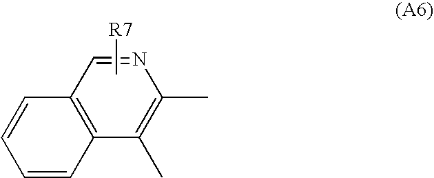
- A may have a molecular structure represented by a formula (A6) below:
- R7 may be a hydrogen atom, a halogen atom or a substituent.
- A may have a molecular structure represented by a formula (A7) below:
- R8 may be a hydrogen atom, a halogen atom or a substituent.
- A may have a molecular structure represented by a formula (A8) below:
- R9 may be a hydrogen atom, a halogen atom or a substituent.
- A may have a molecular structure represented by a formula (A9) below:
- R10 may be a hydrogen atom, a halogen atom or a substituent.
- A may have a molecular structure represented by a formula (A10) below:
- R11 may be a hydrogen atom, a halogen atom or a substituent.
- A may have a molecular structure represented by a formula (A11) below:
- R12 may be a hydrogen atom, a halogen atom or a substituent.
- the compound composed of iridium and the quinoline derivative has a molecular structure represented by a formula (2) below:
- R21 is a hydrogen atom, a halogen atom or a substituent
- A is a substituent
- D is a substituent forming a ring.
- D may have a molecular structure represented by a formula (D1) below:
- R22 and R23 which may be identical to or different from each other, may be a hydrogen atom, a halogen atom or a substituent.
- D may have a molecular structure represented by a formula (D2) below:
- R24 may be a hydrogen atom, a halogen atom or a substituent.
- A may have a molecular structure represented by a formula (A12) below:
- R13 may be a hydrogen atom, a halogen atom or a substituent.
- A may have a molecular structure represented by a formula (A13) below:
- R14 may be a hydrogen atom, a halogen atom or a substituent.
- A may have a molecular structure represented by a formula (A14) below:
- R15 may be a hydrogen atom, a halogen atom or a substituent.
- A may have a molecular structure represented by a formula (A15) below:
- R16 may be a hydrogen atom, a halogen atom or a substituent.
- A may have a molecular structure represented by a formula (A16) below:
- R17 may be a hydrogen atom, a halogen atom or a substituent.
- the compound composed of iridium and a quinoline derivative may be tris(2-phenylquinoline)iridium having a molecular structure represented by a formula (8) below.
- the luminescent layer may further include a host material, and the content of the compound composed of iridium and the quinoline derivative may be not less than 0.1 wt % nor more than 50 wt % for the host material. As described above, even if the compound composed of iridium and a quinoline derivative is added as a dopant to the luminescent layer, red-orange light with high luminance can be obtained at high luminous efficiency.
- the host material may be 4,4′-bis(carbazol-9-yl)biphenyl having the molecular structure represented by a formula (9) shown below.
- a hole blocking layer with a larger ionization potential than that of the luminescent layer is preferably provided between the luminescent layer and the electron injection electrode.
- the provision of such a hole blocking layer results in an increase in the energy barrier between the luminescent layer and the hole blocking layer. This makes it possible to prevent the injection of holes from the luminescent layer to the electron injection electrode and thus re-couple electrons and holes at high efficiency in the luminescent layer. This enables improvements in the luminous efficiency of the organic EL devices.
- a luminescent material according to another aspect of the present invention has a molecular structure represented by a formula (2) below:
- R21 is a hydrogen atom, a halogen atom or a substituent
- A is a substituent
- D is a substituent forming a ring.
- D may have a molecular structure represented by a formula (D1) below:
- R22 and R23 which may be identical to or different from each other, may be a hydrogen atom, a halogen atom or a substituent.
- D may have a molecular structure represented by a formula (D2) below:
- R24 may be a hydrogen atom, a halogen atom or a substituent.
- Such a luminescent material can emit red-orange light since it is such a material that can emit light via a triplet excited state.
- An organic compound according to still another aspect of the present invention has a molecular structure represented by a formula (2) shown below:
- R21 is a hydrogen atom, a halogen atom or a substituent
- A is a substituent
- D is a substituent forming a ring.
- D may have a molecular structure represented by a formula (D1) shown below:
- R22 and R23 which may be identical to or different from each other, may be a hydrogen atom, a halogen atom or a substituent.
- D may have a molecular structure represented by a formula (D2) shown below:
- R24 may be a hydrogen atom, a halogen atom or a substituent.
- the organic compound may have a molecular structure represented by a formula (C1) shown below.
- the organic compound may have a molecular structure represented by a formula (C2) shown below.
- the organic compound may have a molecular structure represented by a formula (C7) shown below.
- the organic compound may have a molecular structure represented by a formula (C8) shown below.
- Such an organic compound can emit red-orange light since it is such a material that can emit light via a triplet excited state.
- FIG. 1 is a schematic diagram showing the structure of an organic EL device according to one embodiment of the present invention.
- FIG. 2 is a diagram showing a luminescent spectrum in the organic EL device of the embodiment.
- FIG. 1 is a schematic diagram showing the structure of an organic electroluminescence (hereinafter referred to as an organic EL device) according to one embodiment of the present invention.
- a hole injection electrode (an anode) 2 composed of a transparent electrode film is formed on a glass substrate 1 , in an organic EL device 100 .
- a hole injection layer 3 , a hole transport layer 4 and a luminescent layer 5 all made of respective organic materials are formed in turn on the hole injection electrode 2 .
- a hole blocking layer 6 made of organic materials is formed on the luminescent layer 5 , and an electron injection electrode (a cathode) 7 is formed on the hole blocking layer 6 .
- the luminescent layer 5 includes an organic iridium compound composed of a quinoline derivative and iridium being metal.
- the luminescent layer 5 per se may be composed of such an organic iridium compound.
- the layer 5 may include such an organic iridium compound as a luminescent dopant.
- the organic iridium compound composed of iridium and the quinoline derivative is contained as the luminescent dopant in a host material which will be described later.
- the content of this organic iridium compound is 0.1 wt % to 50 wt %, preferably 1 wt % to 10 wt % for the host material.
- CBP 4,4′-bis(carbazol-9-yl)biphenyl
- the above described organic iridium compound contained in the luminescent layer 5 has such a molecular structure as represented by a formula (1) shown below:
- R1 represents a hydrogen atom, a halogen atom or a substituent
- A represents a substituent which will be described later.
- A may be any one of substituents each having such molecular structures as represented by, for example, respective formulas (A1) to (A11).
- R2 to R12 are a hydrogen atom, a halogen atom or a substituent.
- the organic iridium compound composed of iridium and the quinoline derivative, represented by the above formula (1) is capable of emitting phosphorescence of red to orange via a triplet excited state.
- the organic iridium compound represented by the above formula (1) is produced by making the reaction between a quinoline derivative having a molecular structure represented by a formula (B1) shown below and an iridium compound, in which reaction the quinoline derivative is coordinated or chelated with iridium. In this case, not less than 3 mol of the quinoline derivative is reacted with 1 mol of the iridium compound.
- a quinoline derivative having a molecular structure represented by a formula (B1) shown below
- an iridium compound in which reaction the quinoline derivative is coordinated or chelated with iridium. In this case, not less than 3 mol of the quinoline derivative is reacted with 1 mol of the iridium compound.
- the iridium compound tris(acetylacetonato)iridium (Ir(acac) 3 ), or iridium chloride or the like can be employed.
- acac is an abbreviation of “acetylace
- the light emission which is caused when electrons being in the singlet excited state out of such two types of excited states transit to a ground state is called fluorescence.
- fluorescence is generated based on a spin allowable state and easily occurs.
- the fluorescence is applied in wide use for luminescent phenomena such as of organic EL devices and the like.
- the light emission which is caused when electrons being in the triplet excited state transit to the ground state is called phosphorescence.
- the phosphorescence is generated based on a spin inhibited state. According to Pauli's exclusion principle, it is not possible that two electrons with parallel electron spin exist on the same electron orbit (which corresponds to the ground state in this case). Therefore, the electron spin of electrons which may transit is required to be inverted by receiving some perturbation, in order that the electrons being in the triplet excited state may transit to the ground state and emit light.
- the inversion of electron spin is difficult in most of luminescent substances which are usually used for the organic EL devices. Therefore, as for normal substances, phosphorescence is known as a special phenomenon which is observed only in a very low temperature area equal to or below a liquid nitrogen temperature.
- the above described DCM-based material employed as luminescent materials for a conventional red light emitting organic EL device emits red fluorescence via the singlet excited state, and thus this material cannot effectively utilize the triplet excited state covering approximately 3 ⁇ 4 of the entire excited state. It is therefore difficult to achieve the increased luminous efficiency in the organic EL devices having the luminescent layer made of such DCM-based red luminescent materials.
- the luminescent layer 5 includes, as the red-orange light emitting materials, the organic iridium compound having the structure represented by the above formula (1), the luminescent layer 5 can emit red-orange phosphorescence via the triplet excited state.
- the triplet excited state covering approximately 3 ⁇ 4 of the entire excited state, in this case. This makes it possible to obtain red-orange light with high luminance and at high luminous efficiency in the organic EL device 100 .
- organic iridium compound having a structure similar to that of the organic iridium compound having the molecular structure represented by the above formula (1).
- the disclosed organic iridium compound is, however, a compound comprised of a combination of phenylpyridine and iridium, and hence its ⁇ conjugated electron system is shorter than that of the compound comprised of the combination of the quinoline derivative and iridium as in this embodiment. Therefore, the color of light emitted from the organic iridium compound composed of phenylpyridine and iridium disclosed in the above document is green.
- the organic iridium compound composed of the combination of the quinoline derivative and iridium since the organic iridium compound composed of the combination of the quinoline derivative and iridium is employed, its ⁇ conjugated electron system can be extended compared to that of the above compound composed of phenylpyridine and iridium. This makes it possible to shift a spectrum to a red-orange area, thereby realizing the organic EL device capable of emitting red-orange light in this embodiment.
- the above organic iridium compound contained in the luminescent layer 5 preferably has the molecular structure represented by a formula (2) shown below.
- R21 represents a hydrogen atom, a halogen atom or a substituent
- A represents a substituent which will be described later
- D represents a substituent forming a ring which will be described later.
- D may be a substituent having a molecular structure represented by, for example, a formula (D1) or (D2) shown below.
- R22 to R24 are a hydrogen atom, a halogen atom or a substituent.
- A may be any one of substituents having the molecular structures represented by, for example, formulas (A12) to (A16) shown below.
- R13 to R17 are a hydrogen atom, a halogen atom or a substituent.
- the organic iridium compound composed of iridium and the quinoline derivative, represented by the above formula (2) is capable of emitting phosphorescence of red to orange via a triplet excited state.
- the organic iridium compound represented by the above formula (2) is produced by the reaction among a quinoline derivative having a molecular structure represented by a formula (B2) shown below, an iridium compound and a compound corresponding to D represented by the above formula (D1) or (D2), in which reaction the quinoline derivative and D are coordinated or chelated with iridium.
- a quinoline derivative having a molecular structure represented by a formula (B2) shown below an iridium compound and a compound corresponding to D represented by the above formula (D1) or (D2), in which reaction the quinoline derivative and D are coordinated or chelated with iridium.
- 1.5 to 2.5 mol of the quinoline derivative and 0.5 to 1.5 mol of the compound corresponding to D are reacted with 1 mol of the iridium compound.
- the iridium compound tris(acetylacetonato)iridium (Ir(acac) 3 ), or iridium chloride or the like can
- the structure of the organic EL device according to the present invention is not limited to the above structure, but can apply various structures.
- such a structure may be applied that only two layers, which are the luminescent layer and the electron transport layer are provided between the hole injection electrode 2 and the electron injection electrode 7 .
- such a structure may be applied that the hole transport layer, the luminescent layer, the hole blocking layer and the electron transport layer are stacked in turn between the hole injection electrode 2 and the electron injection electrode 7 .
- a hole blocking layer having a larger ionization potential than that of the luminescent layer is preferably provided between the luminescent layer and the electron injection electrode in the organic EL device. Provision of this hole blocking layer enables the increased energy barrier between the luminescent layer and the hole blocking layer. This can prevent the injection of holes from the luminescent layer to the layers on the side of the electron injection electrode (e.g., the electron transport layer and the electron injection layer), enabling the re-coupling of holes and electrons in the luminescent layer at high efficiency. This results in improvements in the luminous efficiency in the organic EL device.
- the luminescent layer 5 when a voltage is applied across the hole injection electrode 2 and the electron injection electrode 7 , the luminescent layer 5 emits red-orange light, and light is emitted from the back face of the glass substrate 1 .
- Respective organic EL devices of inventive examples 1 to 3 and a comparative example were manufactured, and their luminescent characteristics were measured as in the following.
- such an organic EL device was used that a hole injection electrode (an anode), a hole transport layer, a luminescent layer, a hole blocking layer, an electron transport layer and an electron injection electrode (a cathode) were stacked in turn on a glass substrate.
- the hole injection electrode of the organic EL device is composed of indium-tin oxides (ITO) with a 1000 ⁇ thickness.
- the hole transport layer has a 500 ⁇ thickness and is composed of N,N′-Di(naphthalen-1-yl)-N,N′-diphenylbenzidine (hereinafter referred to as NPB) having the molecular structure represented by a formula (11) as shown below.
- the luminescent layer 5 has a 200 ⁇ thickness, and it contains, as a host material, CBP having the molecular structure represented by a formula (9) shown below and contains, as a red-orange luminescent dopant, tris(2-phenylquinoline)iridium (hereinafter referred to as Ir(Phq) 3 ) having the molecular structure represented by a formula (8) shown below.
- This Ir(Phq) 3 can emit red-orange light via the triplet excited state.
- the luminescent layer 5 contains 6.5 wt % of Ir(Phq) 3 for the CBP serving as the host material. Further, the ionization potential of CBP is 5.9 eV.
- the hole blocking layer has a 100 ⁇ thickness and is composed of Bathocuproine (hereinafter referred to as BCP) having the molecular structure represented by a formula (12).
- BCP Bathocuproine
- the ionization potential of the hole blocking layer composed of BCP is 6.2 eV, which is larger than that of CBP serving as the host material of the luminescent layer.
- the electron transport layer has a 150 ⁇ thickness and is composed of tris(8-hydroxyquinolinato)aluminum (hereinafter referred to as Alq) having the molecular structure represented by a formula (13).
- Alq tris(8-hydroxyquinolinato)aluminum
- the ionization potential of the electron transport layer composed of Alq is 5.5 eV.
- the energy barrier generated between the luminescent layer and the hole blocking layer becomes increased in the organic EL device of the inventive example 1, in which the hole blocking layer with a large ionization potential as described above is formed between the luminescent layer and the electron transport layer. This can prevent the injection of holes from the luminescent layer to the electron transport layer. This enables the re-coupling of holes and electrons in the luminescent layer at high efficiency. This results in improvements of luminous efficiency in the organic EL device.
- the electron injection electrode is composed of a MgIn alloy (a ratio of 10 to 1) with a 2000 ⁇ thickness.
- the organic EL device having the above described structure was manufactured as in the following manner.
- the hole injection electrode made of indium-tin oxides (ITO) was formed on the glass substrate. Then, the glass substrate with the hole injection electrode formed thereon was cleaned with a neutral detergent, followed by ultrasonic cleaning in acetone for 10 minutes and in ethanol for 10 minutes. Further, the surface of the glass substrate was cleaned in an ozone cleaner.
- ITO indium-tin oxides
- the hole transport layer, the luminescent layer, the hole blocking layer, the electron transport layer and the electron injection electrode were stacked in turn by a vacuum vapor deposition on the above hole injection electrode made of ITO.
- This vapor deposition was conducted under conditions of ordinary temperatures without control of substrate temperatures at the degree of vacuum of 1 ⁇ 10 ⁇ 6 Torr.
- a positive bias voltage was applied to the hole injection electrode of the organic EL device manufactured by the above method, while a negative bias voltage was applied to the electron injection electrode, so that the luminescent characteristics of the device were measured.
- the maximal luminance of the organic EL device was 34,200 cd/m 2 , and the luminous efficiency at that time was 15.7 cd/A.
- an organic EL device was employed that has the same structure as that of the organic EL device of the inventive example 1 except for the following points.
- the organic EL device of the inventive example 2 was manufactured by the same method as that of the organic EL device of the inventive example 1.
- the hole blocking layer is composed of (1,1′-Bisphenyl)-4-Olato)(2-methyl-8-quinolinolate-N1,08)Aluminum (hereinafter referred to as BAlq) having the molecular structure represented by a formula (14) shown below.
- BAlq (1,1′-Bisphenyl)-4-Olato)(2-methyl-8-quinolinolate-N1,08)Aluminum
- the energy barrier generated between the luminescent layer and the hole blocking layer is increased, thereby preventing the injection of holes from the luminescent layer to the electron transport layer.
- This enables the re-coupling of holes and electrons in the luminescent layer at high efficiency.
- the luminescent characteristics of the above organic EL device were measured by the same method as that applied in the inventive example 1. Consequently, excellent orange light with a peak at a 583 nm wavelength was obtained in this organic EL device.
- an organic EL device was employed that has the same structure as that of the organic EL device of the inventive example 1 except that the luminescent layer does not include any host material and is composed of only a single layer of Ir(Phq) 3 with a 200 ⁇ thickness.
- the organic EL device of the inventive example 3 was manufactured by the same method as that of the organic EL device of the inventive example 1.
- the hole blocking layer with a large ionization potential is formed between the luminescent layer and the electron transport layer, the energy barrier generated between the luminescent layer and the hole blocking layer becomes increased. This can prevent the injection of holes from the luminescent layer to the electron transport layer, thereby enabling the re-coupling of holes and electrons in the luminescent layer at high efficiency. This results in improvements of the luminous efficiency of the organic EL device.
- an organic EL device was employed that has the same structure as that of the inventive example 1 except that as the red-orange luminescent dopant of the luminescent layer, Ir(Phq) 3 was replaced with 5,10,15,20-Tetraphenyl-21H,23H-porphine (hereinafter referred to as TPP) having the structure represented by a formula (15) shown below.
- TPP 5,10,15,20-Tetraphenyl-21H,23H-porphine
- This organic EL device of the comparative example was manufactured by the same method as that applied to the organic EL device of the inventive example 1.
- the TPP contained as the red-orange luminescent dopant in the luminescent layer is a substance that emits red-orange light via the singlet excited state.
- the luminance and the luminous efficiency are more increased in the case where the luminescent layer contains BCP or BAlq as a host as compared with the case where the luminescent layer is composed of only Ir(Phq) 3 .
- organic EL devices were employed that each has the same structure as that of the organic EL device of the inventive example 1 except for the dopant of the luminescent layer.
- the organic EL devices of the inventive examples 4 to 13 were manufactured by the same method as that applied to the organic EL device of the inventive example 1.
- FIG. 2 representatively shows the luminescent spectrum of the organic EL device in the inventive example 11.
- the luminescent spectrum having a peak at a 630 nm wavelength was obtained in the organic EL device of the inventive example 11, as shown in FIG. 2 .
- Table 1 shows the results of measurement of the materials and the luminescent characteristics of the organic EL devices in the inventive examples 4 to 13.
- inventive examples 14 to 16 such organic EL devices were employed that each has the same structure as that of the organic EL device in the inventive example 1 except that the above compound 3 was used as the dopants of the luminescent layers.
- concentrations of the respective compounds 3 used as the dopants were set to 13%, 20%, 3%, respectively, in the organic EL devices of the inventive examples 14 to 16.
- the organic EL devices of the inventive examples 14 to 16 were manufactured by the same method as that applied to the organic EL device of the inventive example 1.
- the luminescent characteristics of the above organic EL devices were measured by the same method as that applied to the inventive example 1.
- the above Table 1 shows the results of measurement of the materials and the luminescent characteristics of the organic EL devices in the inventive examples 14 to 16.
- the maximal luminance was 43,000 cd/m 2 and the luminous efficiency was 18.2 cd/A.
- the concentration of the compound 3 as the dopant was 6.5%
- the maximal luminance was 29,500 cd/m 2 and the luminous efficiency was 14.2 cd/A.
- the concentration of the compound 3 as the dopant was 3%
- the maximal luminance was 20,100 cd/m 2 and the luminous efficiency was 10.2 cd/A.
- the concentration of the compound 3 as the dopant was 20%
- the maximal luminance was 17,000 cd/m 2
- the luminous efficiency was 8 cd/A. From the results of the inventive examples 6, 14 to 16, it was apparent that excellent luminous efficiency was realized when the concentration of the compound 3 was from 3% to 20%.
- an organic iridium compound was employed as a host material for the luminescent layer.
- an organic EL device having the same structure as that of the organic EL device in the inventive example 1 was used except that the luminescent layer contains Ir(Phq) 3 as a host material and contains 6.5 wt % of the compound 8 represented by the above formula (C8) as a luminescent dopant.
- the organic EL device of the inventive example 17 was manufactured by the same method as that of the organic EL device of the inventive example 1.
- an organic iridium compound was employed as a hole transport material.
- such an organic El device was used that a hole injection electrode made of ITO, a hole transport layer of 30 nm made of Ir(Phq) 3 , a luminescent layer of 50 nm made of Alq, and an electron injection electrode made of a MgIn alloy were stacked in turn on a glass substrate.
- an organic iridium compound was used as an electron transport material.
- such an organic EL device was employed that a hole injection electrode made of ITO, a luminescent layer of 50 nm, an electron transport layer of 30 nm made of Ir(Phq) 3 , and an electron injection electrode made of a MgIn alloy are stacked in turn on a glass substrate.
- the luminescent layer contains NPB as a host material and contains as a luminescent dopant 5 wt % of rubrene having a molecular structure represented by a formula (16) below.
Abstract
Description


where R1 is a hydrogen atom, a halogen atom or a substituent, and that A is a substituent.

where R2 may be a hydrogen atom, a halogen atom or a substituent.

where R3 may be a hydrogen atom, a halogen atom or a substituent.

where R4 may be a hydrogen atom, a halogen atom or a substituent.

where R5 may be a hydrogen atom, a halogen atom or a substituent.

where R6 may be a hydrogen atom, a halogen atom or a substituent.
where R7 may be a hydrogen atom, a halogen atom or a substituent.

where R8 may be a hydrogen atom, a halogen atom or a substituent.

where R9 may be a hydrogen atom, a halogen atom or a substituent.

where R10 may be a hydrogen atom, a halogen atom or a substituent.

where R11 may be a hydrogen atom, a halogen atom or a substituent.

where R12 may be a hydrogen atom, a halogen atom or a substituent.

where R21 is a hydrogen atom, a halogen atom or a substituent, A is a substituent, and D is a substituent forming a ring.

where R22 and R23, which may be identical to or different from each other, may be a hydrogen atom, a halogen atom or a substituent.

where R24 may be a hydrogen atom, a halogen atom or a substituent.

where R13 may be a hydrogen atom, a halogen atom or a substituent.

where R14 may be a hydrogen atom, a halogen atom or a substituent.

where R15 may be a hydrogen atom, a halogen atom or a substituent.

where R16 may be a hydrogen atom, a halogen atom or a substituent.

where R17 may be a hydrogen atom, a halogen atom or a substituent.


where R21 is a hydrogen atom, a halogen atom or a substituent, A is a substituent, and D is a substituent forming a ring.

where R22 and R23, which may be identical to or different from each other, may be a hydrogen atom, a halogen atom or a substituent.

where R24 may be a hydrogen atom, a halogen atom or a substituent.


where R1 represents a hydrogen atom, a halogen atom or a substituent, and A represents a substituent which will be described later.


| TABLE 1 | ||||||||||
| Lumi- | ||||||||||
| Maximal | nous | |||||||||
| Hole | Hole | Electron | Lumi- | Luminous | Wave- | Chromaticity | ||||
| Transport | Blocking | Transport | nance | Efficiency | length | Coordinate | ||||
| Anode | Layer | Luminescent Layer | Layer | Layer | Cathode | (cd/m2) | (cd/A) | (nm) | (x, y) | |
| Inventive | ITO | NPB | CBP(host) + 6.5% compound1 | BCP | Alq | MgIn | 12,300 | 5.4 | 625 | 0.64, 0.35 |
| Example 4 | (dopant) | |||||||||
| Inventive | ITO | NPB | CBP(host) + 6.5% compound2 | BCP | Alq | MgIn | 15,800 | 5.6 | 629 | 0.65, 0.34 |
| Example 5 | (dopant) | |||||||||
| Inventive | ITO | NPB | CBP(host) + 6.5% compound3 | BCP | Alq | MgIn | 29,500 | 14.2 | 590 | 0.56, 0.43 |
| Example 6 | (dopant) | |||||||||
| Inventive | ITO | NPB | CBP(host) + 6.5% compound4 | BCP | Alq | MgIn | 11,000 | 4.8 | 623 | 0.64, 0.35 |
| Example 7 | (dopant) | |||||||||
| Inventive | ITO | NPB | CBP(host) + 6.5% compound5 | BCP | Alq | MgIn | 21,000 | 11.4 | 583 | 0.53, 0.46 |
| Example 8 | (dopant) | |||||||||
| Inventive | ITO | NPB | CBP(host) + 6.5% compound6 | BCP | Alq | MgIn | 11,200 | 4.8 | 630 | 0.65, 0.34 |
| Example 9 | (dopant) | |||||||||
| Inventive | ITO | NPB | CBP(host) + 6.5% compound7 | BCP | Alq | MgIn | 11,000 | 4.7 | 625 | 0.64, 0.35 |
| Example | (dopant) | |||||||||
| 10 | ||||||||||
| Inventive | ITO | NPB | CBP(host) + 6.5% compound8 | BCP | Alq | MgIn | 11,000 | 4.7 | 630 | 0.65, 0.34 |
| Example 11 | (dopant) | |||||||||
| Inventive | ITO | NPB | CBP(host) + 6.5% compound9 | BCP | Alq | MgIn | 10,000 | 4.3 | 623 | 0.64, 0.35 |
| Example | (dopant) | |||||||||
| 12 | ||||||||||
| Inventive | ITO | NPB | CBP(host) + 6.5% compound10 | BCP | Alq | MgIn | 23,000 | 12.3 | 585 | 0.53, 0.46 |
| Example | (dopant) | |||||||||
| 13 | ||||||||||
| Inventive | ITO | NPB | CBP(host) + 13% compound3 | BCP | Alq | MgIn | 43,000 | 18.2 | 602 | 0.58, 0.42 |
| Example | (dopant) | |||||||||
| 14 | ||||||||||
| Inventive | ITO | NPB | CBP(host) + 20% compound3 | BCP | Alq | MgIn | 17,000 | 8 | 605 | 0.58, 0.42 |
| Example | (dopant) | |||||||||
| 15 | ||||||||||
| Inventive | ITO | NPB | CBP(host) + 3% compound3 | BCP | Alq | MgIn | 20,100 | 10.2 | 574 | 0.53, 0.46 |
| Example | (dopant) | |||||||||
| 16 | ||||||||||

Claims (2)


Applications Claiming Priority (5)
| Application Number | Priority Date | Filing Date | Title |
|---|---|---|---|
| JP2001036634 | 2001-02-14 | ||
| JP2001-36634 | 2001-02-14 | ||
| JP2001-036634 | 2001-12-13 | ||
| JP2002-030753 | 2002-02-07 | ||
| PCT/JP2002/001162 WO2002064700A1 (en) | 2001-02-14 | 2002-02-12 | Organic electroluminescence device, lumincescent material, and organic compound |
Publications (2)
| Publication Number | Publication Date |
|---|---|
| US20040142208A1 US20040142208A1 (en) | 2004-07-22 |
| US7998595B2 true US7998595B2 (en) | 2011-08-16 |
Family
ID=32697392
Family Applications (1)
| Application Number | Title | Priority Date | Filing Date |
|---|---|---|---|
| US10/467,856 Active 2025-07-03 US7998595B2 (en) | 2001-02-14 | 2002-02-12 | Organic electroluminescent device, luminescent material and organic compound |
Country Status (1)
| Country | Link |
|---|---|
| US (1) | US7998595B2 (en) |
Families Citing this family (12)
| Publication number | Priority date | Publication date | Assignee | Title |
|---|---|---|---|---|
| KR101016164B1 (en) | 2002-10-09 | 2011-02-17 | 이데미쓰 고산 가부시키가이샤 | Organic electroluminescent device |
| WO2006135076A1 (en) * | 2005-06-14 | 2006-12-21 | Showa Denko K.K. | Light emitting polymer material, organic electroluminescence device and display device comprising light emitting polymer material |
| US7709105B2 (en) * | 2005-12-14 | 2010-05-04 | Global Oled Technology Llc | Electroluminescent host material |
| US7659022B2 (en) * | 2006-08-14 | 2010-02-09 | Modine Manufacturing Company | Integrated solid oxide fuel cell and fuel processor |
| US8518556B2 (en) * | 2006-01-27 | 2013-08-27 | Konica Minolta Holdings, Inc. | Electroluminescent element |
| WO2008069322A1 (en) | 2006-12-08 | 2008-06-12 | National Institute Of Advanced Industrial Science And Technology | Metal coordination compound and light-emitting material using the same |
| KR100910153B1 (en) * | 2007-11-20 | 2009-07-30 | (주)그라쎌 | Novel red electroluminescent compounds and organic electroluminescent device using the same |
| JP4751954B1 (en) * | 2010-07-09 | 2011-08-17 | 富士フイルム株式会社 | Organic electroluminescence device |
| KR20140083413A (en) * | 2012-12-26 | 2014-07-04 | 엘지디스플레이 주식회사 | Red Phosphorescent Compounds and Organic Electroluminescent Device Using the Same |
| CN103113413B (en) * | 2013-02-07 | 2016-03-02 | 合肥京东方光电科技有限公司 | Dicyclo complex of iridium and preparation method, organic electroluminescence device and preparation method |
| CN104178114A (en) * | 2013-05-22 | 2014-12-03 | 海洋王照明科技股份有限公司 | Red phosphorescence iridium complexes, preparing method thereof and organic electroluminescence device |
| US11623936B2 (en) * | 2018-12-11 | 2023-04-11 | Universal Display Corporation | Organic electroluminescent materials and devices |
Citations (11)
| Publication number | Priority date | Publication date | Assignee | Title |
|---|---|---|---|---|
| KR20000075253A (en) | 1999-05-31 | 2000-12-15 | 김순택 | Blue light-emitting compound and display device adopting blue light-emitting compound as color-developing substance |
| WO2001041512A1 (en) | 1999-12-01 | 2001-06-07 | The Trustees Of Princeton University | Complexes of form l2mx as phosphorescent dopants for organic leds |
| US20010019782A1 (en) | 1999-12-27 | 2001-09-06 | Tatsuya Igarashi | Light-emitting material comprising orthometalated iridium complex, light-emitting device, high efficiency red light-emitting device, and novel iridium complex |
| JP2001247859A (en) | 1999-12-27 | 2001-09-14 | Fuji Photo Film Co Ltd | Luminescent element material comprising ortho metallized iridium complex, luminescent element and novel iridium complex |
| JP2001345183A (en) | 2000-03-28 | 2001-12-14 | Fuji Photo Film Co Ltd | Highly efficient red light emitting element, light emitting element material composed of iridium complex and novel iridium complex |
| WO2002002714A2 (en) | 2000-06-30 | 2002-01-10 | E.I. Du Pont De Nemours And Company | Electroluminescent iridium compounds with fluorinated phenylpyridines, phenylpyrimidines, and phenylquinolines and devices made with such compounds |
| US20020034656A1 (en) * | 1998-09-14 | 2002-03-21 | Thompson Mark E. | Organometallic complexes as phosphorescent emitters in organic LEDs |
| EP1191612A2 (en) | 2000-09-26 | 2002-03-27 | Canon Kabushiki Kaisha | Luminescence device, display apparatus and metal coordination compound |
| US20020055014A1 (en) | 2000-08-24 | 2002-05-09 | Fuji Photo Film Co., Ltd. | Light-emitting device and material therefor |
| EP1238981A2 (en) | 2001-03-08 | 2002-09-11 | Canon Kabushiki Kaisha | Metal coordination compound, luminescence device and display apparatus |
| JP2003081989A (en) | 2000-12-01 | 2003-03-19 | Canon Inc | Metal coordination compound, light emitting element and display |
Family Cites Families (2)
| Publication number | Priority date | Publication date | Assignee | Title |
|---|---|---|---|---|
| US20020019782A1 (en) * | 2000-08-04 | 2002-02-14 | Arie Hershtik | Shopping method |
| US7250512B2 (en) * | 2001-11-07 | 2007-07-31 | E. I. Du Pont De Nemours And Company | Electroluminescent iridium compounds having red-orange or red emission and devices made with such compounds |
-
2002
- 2002-02-12 US US10/467,856 patent/US7998595B2/en active Active
Patent Citations (20)
| Publication number | Priority date | Publication date | Assignee | Title |
|---|---|---|---|---|
| US20020034656A1 (en) * | 1998-09-14 | 2002-03-21 | Thompson Mark E. | Organometallic complexes as phosphorescent emitters in organic LEDs |
| US6312839B1 (en) | 1999-05-31 | 2001-11-06 | Samsung Display Devices Co., Ltd. | Blue-light emitting compound and display device adopting the same as color developing substance |
| KR20000075253A (en) | 1999-05-31 | 2000-12-15 | 김순택 | Blue light-emitting compound and display device adopting blue light-emitting compound as color-developing substance |
| WO2001041512A1 (en) | 1999-12-01 | 2001-06-07 | The Trustees Of Princeton University | Complexes of form l2mx as phosphorescent dopants for organic leds |
| JP2003515897A (en) | 1999-12-01 | 2003-05-07 | ザ、トラスティーズ オブ プリンストン ユニバーシティ | Complexes of Formula L2MX as phosphorescent dopants for organic LEDs |
| US20010019782A1 (en) | 1999-12-27 | 2001-09-06 | Tatsuya Igarashi | Light-emitting material comprising orthometalated iridium complex, light-emitting device, high efficiency red light-emitting device, and novel iridium complex |
| JP2001247859A (en) | 1999-12-27 | 2001-09-14 | Fuji Photo Film Co Ltd | Luminescent element material comprising ortho metallized iridium complex, luminescent element and novel iridium complex |
| US20050003233A1 (en) | 1999-12-27 | 2005-01-06 | Fuji Photo Film Co., Ltd. | Light-emitting material comprising orthometalated iridium complex, light-emitting device, high efficiency red light-emitting device, and novel iridium complex |
| JP2001345183A (en) | 2000-03-28 | 2001-12-14 | Fuji Photo Film Co Ltd | Highly efficient red light emitting element, light emitting element material composed of iridium complex and novel iridium complex |
| WO2002002714A2 (en) | 2000-06-30 | 2002-01-10 | E.I. Du Pont De Nemours And Company | Electroluminescent iridium compounds with fluorinated phenylpyridines, phenylpyrimidines, and phenylquinolines and devices made with such compounds |
| JP2002319491A (en) | 2000-08-24 | 2002-10-31 | Fuji Photo Film Co Ltd | Light-emitting element and novel polymer organic electroluminescent element |
| US20020055014A1 (en) | 2000-08-24 | 2002-05-09 | Fuji Photo Film Co., Ltd. | Light-emitting device and material therefor |
| US20020063516A1 (en) | 2000-09-26 | 2002-05-30 | Akira Tsuboyama | Limuninescence device, display apparatus and metal coordination compound |
| JP2003081988A (en) | 2000-09-26 | 2003-03-19 | Canon Inc | Light emitting element, display and metal coordination compound for the light emitting element |
| EP1191612A2 (en) | 2000-09-26 | 2002-03-27 | Canon Kabushiki Kaisha | Luminescence device, display apparatus and metal coordination compound |
| US20050025996A1 (en) | 2000-09-26 | 2005-02-03 | Canon Kabushiki Kaisha | Luminescence device, display apparatus and metal coordination compound |
| JP2003081989A (en) | 2000-12-01 | 2003-03-19 | Canon Inc | Metal coordination compound, light emitting element and display |
| US20030054198A1 (en) | 2000-12-01 | 2003-03-20 | Akira Tsuboyama | Metal coordination compound, luminescence device and display apparatus |
| US20050266268A1 (en) | 2000-12-01 | 2005-12-01 | Canon Kabushiki Kaisha | Metal coordination compound, luminescence device and display apparatus |
| EP1238981A2 (en) | 2001-03-08 | 2002-09-11 | Canon Kabushiki Kaisha | Metal coordination compound, luminescence device and display apparatus |
Non-Patent Citations (8)
| Title |
|---|
| C.W. Tang, et al., Appl. Phys. Lett., vol. 51 (12), pp. 913-915 (1987). |
| Chihaya Adachi, et al., Appl. Phys. Lett., vol. 55 (15), pp. 1489-1491 (1989). |
| Japanese Office Action Issued in corresponding Japanese Patent ApplIcation No. 2002-565020, dated Nov. 28, 2006. |
| Korean Office Action, with Partial English Translation, issued in Korean Patent Application No. KR 10-2002-701316 dated on Sep. 25, 2008. |
| M.A. Baldo, et al., "Very High-Efficiency Green Organic Light-Emitting Devices Based on Electrophosphorescence". Applied Physics Letters, Jul. 1999, vol. 75, No. 1, pp. 4-6. |
| S.A. Van Slyke, et al., Appl. Phys. Lett., vol. 69 (15), pp. 2160-2162 (1996). |
| U.S. Appl. No. 60/215,362, filed Jun. 30, 2000. |
| U.S. Appl. No. 60/224,273, filed Aug. 10, 2000. |
Also Published As
| Publication number | Publication date |
|---|---|
| US20040142208A1 (en) | 2004-07-22 |
Similar Documents
| Publication | Publication Date | Title |
|---|---|---|
| US11594697B2 (en) | Non-blocked phosphorescent OLEDs | |
| EP1371708A1 (en) | Organic electroluminescence device, lumincescent material, and organic compound | |
| EP1418217A1 (en) | Organo-electroluminescence element, luminescent material and organic compound | |
| US7611779B2 (en) | Organic electroluminescent device | |
| JP4161262B2 (en) | ORGANIC ELECTROLUMINESCENT ELEMENT AND LIGHT EMITTING OR DISPLAY DEVICE USING THE SAME | |
| EP1624504B1 (en) | OLEDs having inorganic material containing anode capping layer | |
| US7977862B2 (en) | Organic light emitting devices | |
| EP1729327B2 (en) | Use of a phosphorescent iridium compound as emissive molecule in an organic light emitting device | |
| US6451455B1 (en) | Metal complexes bearing both electron transporting and hole transporting moieties | |
| KR101457576B1 (en) | Stabilized White-Emitting OLED Device | |
| KR101760004B1 (en) | Oled device with stabilized yellow light-emitting layer | |
| EP1202358A2 (en) | Organic electroluminescence element | |
| KR100751464B1 (en) | Organic electroluminescent device | |
| US20050147848A1 (en) | Organic electroluminescent device | |
| US7781072B2 (en) | Organic electroluminescence device | |
| US7998595B2 (en) | Organic electroluminescent device, luminescent material and organic compound | |
| US20040151945A1 (en) | Binaphthol based chromophores for the fabrication of blue organic light emitting diodes | |
| USH2084H1 (en) | Pentacene derivatives as red emitters in organic light emitting devices | |
| KR101546089B1 (en) | Organic thin film Materials for Organic Electroluminescent Device and Organic Electroluminescent Device | |
| US6830834B2 (en) | Organic light emitting devices with host-guest bonding | |
| JP4797247B2 (en) | Organic electroluminescence device | |
| JP3547945B2 (en) | Organic electroluminescence device | |
| JP4215476B2 (en) | Organic electroluminescence device |
Legal Events
| Date | Code | Title | Description |
|---|---|---|---|
| AS | Assignment |
Owner name: SANYO ELECTRIC CO., LTD., JAPAN Free format text: ASSIGNMENT OF ASSIGNORS INTEREST;ASSIGNORS:HAMADA, YUJI;MATSUSUE, NORIYUKI;REEL/FRAME:014995/0250 Effective date: 20040210 |
|
| STCF | Information on status: patent grant |
Free format text: PATENTED CASE |
|
| FEPP | Fee payment procedure |
Free format text: PAYOR NUMBER ASSIGNED (ORIGINAL EVENT CODE: ASPN); ENTITY STATUS OF PATENT OWNER: LARGE ENTITY |
|
| FPAY | Fee payment |
Year of fee payment: 4 |
|
| MAFP | Maintenance fee payment |
Free format text: PAYMENT OF MAINTENANCE FEE, 8TH YEAR, LARGE ENTITY (ORIGINAL EVENT CODE: M1552); ENTITY STATUS OF PATENT OWNER: LARGE ENTITY Year of fee payment: 8 |
|
| MAFP | Maintenance fee payment |
Free format text: PAYMENT OF MAINTENANCE FEE, 12TH YEAR, LARGE ENTITY (ORIGINAL EVENT CODE: M1553); ENTITY STATUS OF PATENT OWNER: LARGE ENTITY Year of fee payment: 12 |