US7989264B2 - Warpage resistant semiconductor package and method for manufacturing the same - Google Patents
Warpage resistant semiconductor package and method for manufacturing the same Download PDFInfo
- Publication number
- US7989264B2 US7989264B2 US12/848,472 US84847210A US7989264B2 US 7989264 B2 US7989264 B2 US 7989264B2 US 84847210 A US84847210 A US 84847210A US 7989264 B2 US7989264 B2 US 7989264B2
- Authority
- US
- United States
- Prior art keywords
- semiconductor chip
- electrodes
- semiconductor
- grooves
- chip body
- Prior art date
- Legal status (The legal status is an assumption and is not a legal conclusion. Google has not performed a legal analysis and makes no representation as to the accuracy of the status listed.)
- Active
Links
Images


Classifications
-
- H—ELECTRICITY
- H01—ELECTRIC ELEMENTS
- H01L—SEMICONDUCTOR DEVICES NOT COVERED BY CLASS H10
- H01L21/00—Processes or apparatus adapted for the manufacture or treatment of semiconductor or solid state devices or of parts thereof
- H01L21/70—Manufacture or treatment of devices consisting of a plurality of solid state components formed in or on a common substrate or of parts thereof; Manufacture of integrated circuit devices or of parts thereof
- H01L21/71—Manufacture of specific parts of devices defined in group H01L21/70
- H01L21/768—Applying interconnections to be used for carrying current between separate components within a device comprising conductors and dielectrics
- H01L21/76898—Applying interconnections to be used for carrying current between separate components within a device comprising conductors and dielectrics formed through a semiconductor substrate
-
- H—ELECTRICITY
- H01—ELECTRIC ELEMENTS
- H01L—SEMICONDUCTOR DEVICES NOT COVERED BY CLASS H10
- H01L23/00—Details of semiconductor or other solid state devices
- H01L23/28—Encapsulations, e.g. encapsulating layers, coatings, e.g. for protection
-
- H—ELECTRICITY
- H01—ELECTRIC ELEMENTS
- H01L—SEMICONDUCTOR DEVICES NOT COVERED BY CLASS H10
- H01L23/00—Details of semiconductor or other solid state devices
- H01L23/48—Arrangements for conducting electric current to or from the solid state body in operation, e.g. leads, terminal arrangements ; Selection of materials therefor
- H01L23/481—Internal lead connections, e.g. via connections, feedthrough structures
-
- H—ELECTRICITY
- H01—ELECTRIC ELEMENTS
- H01L—SEMICONDUCTOR DEVICES NOT COVERED BY CLASS H10
- H01L24/00—Arrangements for connecting or disconnecting semiconductor or solid-state bodies; Methods or apparatus related thereto
- H01L24/01—Means for bonding being attached to, or being formed on, the surface to be connected, e.g. chip-to-package, die-attach, "first-level" interconnects; Manufacturing methods related thereto
- H01L24/10—Bump connectors ; Manufacturing methods related thereto
- H01L24/12—Structure, shape, material or disposition of the bump connectors prior to the connecting process
- H01L24/13—Structure, shape, material or disposition of the bump connectors prior to the connecting process of an individual bump connector
-
- H—ELECTRICITY
- H01—ELECTRIC ELEMENTS
- H01L—SEMICONDUCTOR DEVICES NOT COVERED BY CLASS H10
- H01L25/00—Assemblies consisting of a plurality of individual semiconductor or other solid state devices ; Multistep manufacturing processes thereof
- H01L25/03—Assemblies consisting of a plurality of individual semiconductor or other solid state devices ; Multistep manufacturing processes thereof all the devices being of a type provided for in the same subgroup of groups H01L27/00 - H01L33/00, or in a single subclass of H10K, H10N, e.g. assemblies of rectifier diodes
- H01L25/04—Assemblies consisting of a plurality of individual semiconductor or other solid state devices ; Multistep manufacturing processes thereof all the devices being of a type provided for in the same subgroup of groups H01L27/00 - H01L33/00, or in a single subclass of H10K, H10N, e.g. assemblies of rectifier diodes the devices not having separate containers
- H01L25/065—Assemblies consisting of a plurality of individual semiconductor or other solid state devices ; Multistep manufacturing processes thereof all the devices being of a type provided for in the same subgroup of groups H01L27/00 - H01L33/00, or in a single subclass of H10K, H10N, e.g. assemblies of rectifier diodes the devices not having separate containers the devices being of a type provided for in group H01L27/00
- H01L25/0657—Stacked arrangements of devices
-
- H—ELECTRICITY
- H01—ELECTRIC ELEMENTS
- H01L—SEMICONDUCTOR DEVICES NOT COVERED BY CLASS H10
- H01L25/00—Assemblies consisting of a plurality of individual semiconductor or other solid state devices ; Multistep manufacturing processes thereof
- H01L25/50—Multistep manufacturing processes of assemblies consisting of devices, each device being of a type provided for in group H01L27/00 or H01L29/00
-
- H—ELECTRICITY
- H01—ELECTRIC ELEMENTS
- H01L—SEMICONDUCTOR DEVICES NOT COVERED BY CLASS H10
- H01L2224/00—Indexing scheme for arrangements for connecting or disconnecting semiconductor or solid-state bodies and methods related thereto as covered by H01L24/00
- H01L2224/01—Means for bonding being attached to, or being formed on, the surface to be connected, e.g. chip-to-package, die-attach, "first-level" interconnects; Manufacturing methods related thereto
- H01L2224/02—Bonding areas; Manufacturing methods related thereto
- H01L2224/04—Structure, shape, material or disposition of the bonding areas prior to the connecting process
- H01L2224/0401—Bonding areas specifically adapted for bump connectors, e.g. under bump metallisation [UBM]
-
- H—ELECTRICITY
- H01—ELECTRIC ELEMENTS
- H01L—SEMICONDUCTOR DEVICES NOT COVERED BY CLASS H10
- H01L2224/00—Indexing scheme for arrangements for connecting or disconnecting semiconductor or solid-state bodies and methods related thereto as covered by H01L24/00
- H01L2224/01—Means for bonding being attached to, or being formed on, the surface to be connected, e.g. chip-to-package, die-attach, "first-level" interconnects; Manufacturing methods related thereto
- H01L2224/02—Bonding areas; Manufacturing methods related thereto
- H01L2224/04—Structure, shape, material or disposition of the bonding areas prior to the connecting process
- H01L2224/05—Structure, shape, material or disposition of the bonding areas prior to the connecting process of an individual bonding area
- H01L2224/05001—Internal layers
- H01L2224/05099—Material
- H01L2224/051—Material with a principal constituent of the material being a metal or a metalloid, e.g. boron [B], silicon [Si], germanium [Ge], arsenic [As], antimony [Sb], tellurium [Te] and polonium [Po], and alloys thereof
- H01L2224/05138—Material with a principal constituent of the material being a metal or a metalloid, e.g. boron [B], silicon [Si], germanium [Ge], arsenic [As], antimony [Sb], tellurium [Te] and polonium [Po], and alloys thereof the principal constituent melting at a temperature of greater than or equal to 950°C and less than 1550°C
- H01L2224/05155—Nickel [Ni] as principal constituent
-
- H—ELECTRICITY
- H01—ELECTRIC ELEMENTS
- H01L—SEMICONDUCTOR DEVICES NOT COVERED BY CLASS H10
- H01L2224/00—Indexing scheme for arrangements for connecting or disconnecting semiconductor or solid-state bodies and methods related thereto as covered by H01L24/00
- H01L2224/01—Means for bonding being attached to, or being formed on, the surface to be connected, e.g. chip-to-package, die-attach, "first-level" interconnects; Manufacturing methods related thereto
- H01L2224/02—Bonding areas; Manufacturing methods related thereto
- H01L2224/04—Structure, shape, material or disposition of the bonding areas prior to the connecting process
- H01L2224/05—Structure, shape, material or disposition of the bonding areas prior to the connecting process of an individual bonding area
- H01L2224/05001—Internal layers
- H01L2224/05099—Material
- H01L2224/051—Material with a principal constituent of the material being a metal or a metalloid, e.g. boron [B], silicon [Si], germanium [Ge], arsenic [As], antimony [Sb], tellurium [Te] and polonium [Po], and alloys thereof
- H01L2224/05163—Material with a principal constituent of the material being a metal or a metalloid, e.g. boron [B], silicon [Si], germanium [Ge], arsenic [As], antimony [Sb], tellurium [Te] and polonium [Po], and alloys thereof the principal constituent melting at a temperature of greater than 1550°C
- H01L2224/05166—Titanium [Ti] as principal constituent
-
- H—ELECTRICITY
- H01—ELECTRIC ELEMENTS
- H01L—SEMICONDUCTOR DEVICES NOT COVERED BY CLASS H10
- H01L2224/00—Indexing scheme for arrangements for connecting or disconnecting semiconductor or solid-state bodies and methods related thereto as covered by H01L24/00
- H01L2224/01—Means for bonding being attached to, or being formed on, the surface to be connected, e.g. chip-to-package, die-attach, "first-level" interconnects; Manufacturing methods related thereto
- H01L2224/02—Bonding areas; Manufacturing methods related thereto
- H01L2224/04—Structure, shape, material or disposition of the bonding areas prior to the connecting process
- H01L2224/05—Structure, shape, material or disposition of the bonding areas prior to the connecting process of an individual bonding area
- H01L2224/0554—External layer
- H01L2224/0556—Disposition
- H01L2224/0557—Disposition the external layer being disposed on a via connection of the semiconductor or solid-state body
-
- H—ELECTRICITY
- H01—ELECTRIC ELEMENTS
- H01L—SEMICONDUCTOR DEVICES NOT COVERED BY CLASS H10
- H01L2224/00—Indexing scheme for arrangements for connecting or disconnecting semiconductor or solid-state bodies and methods related thereto as covered by H01L24/00
- H01L2224/01—Means for bonding being attached to, or being formed on, the surface to be connected, e.g. chip-to-package, die-attach, "first-level" interconnects; Manufacturing methods related thereto
- H01L2224/02—Bonding areas; Manufacturing methods related thereto
- H01L2224/04—Structure, shape, material or disposition of the bonding areas prior to the connecting process
- H01L2224/05—Structure, shape, material or disposition of the bonding areas prior to the connecting process of an individual bonding area
- H01L2224/0554—External layer
- H01L2224/0556—Disposition
- H01L2224/05571—Disposition the external layer being disposed in a recess of the surface
-
- H—ELECTRICITY
- H01—ELECTRIC ELEMENTS
- H01L—SEMICONDUCTOR DEVICES NOT COVERED BY CLASS H10
- H01L2224/00—Indexing scheme for arrangements for connecting or disconnecting semiconductor or solid-state bodies and methods related thereto as covered by H01L24/00
- H01L2224/01—Means for bonding being attached to, or being formed on, the surface to be connected, e.g. chip-to-package, die-attach, "first-level" interconnects; Manufacturing methods related thereto
- H01L2224/02—Bonding areas; Manufacturing methods related thereto
- H01L2224/04—Structure, shape, material or disposition of the bonding areas prior to the connecting process
- H01L2224/05—Structure, shape, material or disposition of the bonding areas prior to the connecting process of an individual bonding area
- H01L2224/0554—External layer
- H01L2224/05575—Plural external layers
- H01L2224/05576—Plural external layers being mutually engaged together, e.g. through inserts
-
- H—ELECTRICITY
- H01—ELECTRIC ELEMENTS
- H01L—SEMICONDUCTOR DEVICES NOT COVERED BY CLASS H10
- H01L2224/00—Indexing scheme for arrangements for connecting or disconnecting semiconductor or solid-state bodies and methods related thereto as covered by H01L24/00
- H01L2224/01—Means for bonding being attached to, or being formed on, the surface to be connected, e.g. chip-to-package, die-attach, "first-level" interconnects; Manufacturing methods related thereto
- H01L2224/02—Bonding areas; Manufacturing methods related thereto
- H01L2224/04—Structure, shape, material or disposition of the bonding areas prior to the connecting process
- H01L2224/05—Structure, shape, material or disposition of the bonding areas prior to the connecting process of an individual bonding area
- H01L2224/0554—External layer
- H01L2224/05599—Material
- H01L2224/056—Material with a principal constituent of the material being a metal or a metalloid, e.g. boron [B], silicon [Si], germanium [Ge], arsenic [As], antimony [Sb], tellurium [Te] and polonium [Po], and alloys thereof
- H01L2224/05638—Material with a principal constituent of the material being a metal or a metalloid, e.g. boron [B], silicon [Si], germanium [Ge], arsenic [As], antimony [Sb], tellurium [Te] and polonium [Po], and alloys thereof the principal constituent melting at a temperature of greater than or equal to 950°C and less than 1550°C
- H01L2224/05647—Copper [Cu] as principal constituent
-
- H—ELECTRICITY
- H01—ELECTRIC ELEMENTS
- H01L—SEMICONDUCTOR DEVICES NOT COVERED BY CLASS H10
- H01L2224/00—Indexing scheme for arrangements for connecting or disconnecting semiconductor or solid-state bodies and methods related thereto as covered by H01L24/00
- H01L2224/01—Means for bonding being attached to, or being formed on, the surface to be connected, e.g. chip-to-package, die-attach, "first-level" interconnects; Manufacturing methods related thereto
- H01L2224/02—Bonding areas; Manufacturing methods related thereto
- H01L2224/04—Structure, shape, material or disposition of the bonding areas prior to the connecting process
- H01L2224/06—Structure, shape, material or disposition of the bonding areas prior to the connecting process of a plurality of bonding areas
- H01L2224/061—Disposition
- H01L2224/0612—Layout
- H01L2224/0615—Mirror array, i.e. array having only a reflection symmetry, i.e. bilateral symmetry
-
- H—ELECTRICITY
- H01—ELECTRIC ELEMENTS
- H01L—SEMICONDUCTOR DEVICES NOT COVERED BY CLASS H10
- H01L2224/00—Indexing scheme for arrangements for connecting or disconnecting semiconductor or solid-state bodies and methods related thereto as covered by H01L24/00
- H01L2224/01—Means for bonding being attached to, or being formed on, the surface to be connected, e.g. chip-to-package, die-attach, "first-level" interconnects; Manufacturing methods related thereto
- H01L2224/10—Bump connectors; Manufacturing methods related thereto
- H01L2224/12—Structure, shape, material or disposition of the bump connectors prior to the connecting process
- H01L2224/13—Structure, shape, material or disposition of the bump connectors prior to the connecting process of an individual bump connector
- H01L2224/13001—Core members of the bump connector
- H01L2224/13005—Structure
- H01L2224/13009—Bump connector integrally formed with a via connection of the semiconductor or solid-state body
-
- H—ELECTRICITY
- H01—ELECTRIC ELEMENTS
- H01L—SEMICONDUCTOR DEVICES NOT COVERED BY CLASS H10
- H01L2224/00—Indexing scheme for arrangements for connecting or disconnecting semiconductor or solid-state bodies and methods related thereto as covered by H01L24/00
- H01L2224/01—Means for bonding being attached to, or being formed on, the surface to be connected, e.g. chip-to-package, die-attach, "first-level" interconnects; Manufacturing methods related thereto
- H01L2224/10—Bump connectors; Manufacturing methods related thereto
- H01L2224/12—Structure, shape, material or disposition of the bump connectors prior to the connecting process
- H01L2224/13—Structure, shape, material or disposition of the bump connectors prior to the connecting process of an individual bump connector
- H01L2224/13001—Core members of the bump connector
- H01L2224/1302—Disposition
- H01L2224/13025—Disposition the bump connector being disposed on a via connection of the semiconductor or solid-state body
-
- H—ELECTRICITY
- H01—ELECTRIC ELEMENTS
- H01L—SEMICONDUCTOR DEVICES NOT COVERED BY CLASS H10
- H01L2225/00—Details relating to assemblies covered by the group H01L25/00 but not provided for in its subgroups
- H01L2225/03—All the devices being of a type provided for in the same subgroup of groups H01L27/00 - H01L33/648 and H10K99/00
- H01L2225/04—All the devices being of a type provided for in the same subgroup of groups H01L27/00 - H01L33/648 and H10K99/00 the devices not having separate containers
- H01L2225/065—All the devices being of a type provided for in the same subgroup of groups H01L27/00 - H01L33/648 and H10K99/00 the devices not having separate containers the devices being of a type provided for in group H01L27/00
- H01L2225/06503—Stacked arrangements of devices
- H01L2225/06513—Bump or bump-like direct electrical connections between devices, e.g. flip-chip connection, solder bumps
-
- H—ELECTRICITY
- H01—ELECTRIC ELEMENTS
- H01L—SEMICONDUCTOR DEVICES NOT COVERED BY CLASS H10
- H01L2225/00—Details relating to assemblies covered by the group H01L25/00 but not provided for in its subgroups
- H01L2225/03—All the devices being of a type provided for in the same subgroup of groups H01L27/00 - H01L33/648 and H10K99/00
- H01L2225/04—All the devices being of a type provided for in the same subgroup of groups H01L27/00 - H01L33/648 and H10K99/00 the devices not having separate containers
- H01L2225/065—All the devices being of a type provided for in the same subgroup of groups H01L27/00 - H01L33/648 and H10K99/00 the devices not having separate containers the devices being of a type provided for in group H01L27/00
- H01L2225/06503—Stacked arrangements of devices
- H01L2225/06541—Conductive via connections through the device, e.g. vertical interconnects, through silicon via [TSV]
-
- H—ELECTRICITY
- H01—ELECTRIC ELEMENTS
- H01L—SEMICONDUCTOR DEVICES NOT COVERED BY CLASS H10
- H01L2225/00—Details relating to assemblies covered by the group H01L25/00 but not provided for in its subgroups
- H01L2225/03—All the devices being of a type provided for in the same subgroup of groups H01L27/00 - H01L33/648 and H10K99/00
- H01L2225/04—All the devices being of a type provided for in the same subgroup of groups H01L27/00 - H01L33/648 and H10K99/00 the devices not having separate containers
- H01L2225/065—All the devices being of a type provided for in the same subgroup of groups H01L27/00 - H01L33/648 and H10K99/00 the devices not having separate containers the devices being of a type provided for in group H01L27/00
- H01L2225/06503—Stacked arrangements of devices
- H01L2225/06555—Geometry of the stack, e.g. form of the devices, geometry to facilitate stacking
-
- H—ELECTRICITY
- H01—ELECTRIC ELEMENTS
- H01L—SEMICONDUCTOR DEVICES NOT COVERED BY CLASS H10
- H01L23/00—Details of semiconductor or other solid state devices
- H01L23/48—Arrangements for conducting electric current to or from the solid state body in operation, e.g. leads, terminal arrangements ; Selection of materials therefor
- H01L23/488—Arrangements for conducting electric current to or from the solid state body in operation, e.g. leads, terminal arrangements ; Selection of materials therefor consisting of soldered or bonded constructions
- H01L23/498—Leads, i.e. metallisations or lead-frames on insulating substrates, e.g. chip carriers
- H01L23/49811—Additional leads joined to the metallisation on the insulating substrate, e.g. pins, bumps, wires, flat leads
- H01L23/49816—Spherical bumps on the substrate for external connection, e.g. ball grid arrays [BGA]
-
- H—ELECTRICITY
- H01—ELECTRIC ELEMENTS
- H01L—SEMICONDUCTOR DEVICES NOT COVERED BY CLASS H10
- H01L24/00—Arrangements for connecting or disconnecting semiconductor or solid-state bodies; Methods or apparatus related thereto
- H01L24/01—Means for bonding being attached to, or being formed on, the surface to be connected, e.g. chip-to-package, die-attach, "first-level" interconnects; Manufacturing methods related thereto
- H01L24/02—Bonding areas ; Manufacturing methods related thereto
- H01L24/03—Manufacturing methods
-
- H—ELECTRICITY
- H01—ELECTRIC ELEMENTS
- H01L—SEMICONDUCTOR DEVICES NOT COVERED BY CLASS H10
- H01L24/00—Arrangements for connecting or disconnecting semiconductor or solid-state bodies; Methods or apparatus related thereto
- H01L24/01—Means for bonding being attached to, or being formed on, the surface to be connected, e.g. chip-to-package, die-attach, "first-level" interconnects; Manufacturing methods related thereto
- H01L24/02—Bonding areas ; Manufacturing methods related thereto
- H01L24/04—Structure, shape, material or disposition of the bonding areas prior to the connecting process
- H01L24/05—Structure, shape, material or disposition of the bonding areas prior to the connecting process of an individual bonding area
-
- H—ELECTRICITY
- H01—ELECTRIC ELEMENTS
- H01L—SEMICONDUCTOR DEVICES NOT COVERED BY CLASS H10
- H01L24/00—Arrangements for connecting or disconnecting semiconductor or solid-state bodies; Methods or apparatus related thereto
- H01L24/01—Means for bonding being attached to, or being formed on, the surface to be connected, e.g. chip-to-package, die-attach, "first-level" interconnects; Manufacturing methods related thereto
- H01L24/10—Bump connectors ; Manufacturing methods related thereto
-
- H—ELECTRICITY
- H01—ELECTRIC ELEMENTS
- H01L—SEMICONDUCTOR DEVICES NOT COVERED BY CLASS H10
- H01L2924/00—Indexing scheme for arrangements or methods for connecting or disconnecting semiconductor or solid-state bodies as covered by H01L24/00
- H01L2924/0001—Technical content checked by a classifier
- H01L2924/0002—Not covered by any one of groups H01L24/00, H01L24/00 and H01L2224/00
-
- H—ELECTRICITY
- H01—ELECTRIC ELEMENTS
- H01L—SEMICONDUCTOR DEVICES NOT COVERED BY CLASS H10
- H01L2924/00—Indexing scheme for arrangements or methods for connecting or disconnecting semiconductor or solid-state bodies as covered by H01L24/00
- H01L2924/01—Chemical elements
- H01L2924/01078—Platinum [Pt]
-
- H—ELECTRICITY
- H01—ELECTRIC ELEMENTS
- H01L—SEMICONDUCTOR DEVICES NOT COVERED BY CLASS H10
- H01L2924/00—Indexing scheme for arrangements or methods for connecting or disconnecting semiconductor or solid-state bodies as covered by H01L24/00
- H01L2924/15—Details of package parts other than the semiconductor or other solid state devices to be connected
- H01L2924/151—Die mounting substrate
- H01L2924/153—Connection portion
- H01L2924/1531—Connection portion the connection portion being formed only on the surface of the substrate opposite to the die mounting surface
- H01L2924/15311—Connection portion the connection portion being formed only on the surface of the substrate opposite to the die mounting surface being a ball array, e.g. BGA
Definitions
- the present invention relates to a semiconductor package and a method for manufacturing the same.
- the semiconductor chip manufactured through a semiconductor chip manufacturing process has input and output terminals of a very fine size, it is difficult to directly mount the semiconductor chip to a printed circuit board, etc. Also, since the semiconductor chip is likely to break even by small shocks and/or vibrations, the semiconductor chip is generally packaged through a packaging process.
- a semiconductor package having undergone the packaging process has input and output terminals, which are suitable for mounting to a printed circuit board, and does not easily break by externally applied shocks and/or vibrations.
- Embodiments of the present invention are directed to a semiconductor package which has a decreased thickness and which has a propensity to prevent being warped or twisted.
- embodiments of the present invention are directed to a method for manufacturing the semiconductor package.
- the semiconductor package comprises a semiconductor chip having a semiconductor chip body which has a first surface and a second surface facing away from the first surface, through-electrodes which pass through the semiconductor chip body and project from the second surface, and a warpage prevention part which projects in the shape of a fence along an edge of the second surface; and a substrate having a substrate body and connection pads which are formed on an upper surface of the substrate body, facing the second surface, and are connected with the projecting through-electrodes.
- the semiconductor chip body is located in a chip region, and the warpage prevention part is located along scribe line regions which are defined around the chip region.
- a length of the through-electrodes, which project from the second surface, is substantially the same as a height of the warpage prevention part.
- the warpage prevention part is intermittently formed on the second surface.
- the through-electrodes projecting from the second surface include solder members.
- At least two semiconductor chips are located on the substrate.
- the semiconductor package may further comprises bonding pads located on the first surface with the through-electrodes respectively passing through the bonding pads.
- the method for manufacturing the semiconductor package comprises the steps of preparing a semiconductor chip having a first surface, a second surface facing away from the first surface, and a chip region partitioned by scribe regions; forming through-electrodes which pass through the first surface and the second surface; selectively etching the chip region on the second surface of the semiconductor chip to project the through-electrodes and a warpage prevention part, corresponding to the scribe regions, from the etched second surface; and connecting the through-electrodes projecting from the second surface of the semiconductor chip and connection pads of a substrate, corresponding to the through-electrodes, using conductive members.
- the step of forming the through-electrodes comprises the steps of defining grooves which pass through bonding pads formed to on the first surface and have a depth less than a thickness of the semiconductor chip; and filling the grooves with a metal.
- the method may further comprise the step of forming a metal seed layer on inner surfaces of the grooves.
- the step of projecting the warpage prevention part comprises the steps of grinding the second surface and exposing the through-electrodes; covering the scribe regions on the second surface with a photoresist pattern, and exposing the chip region on the second surface; and etching the chip region on the second surface using the photoresist pattern as an etch mask.
- the photoresist pattern is removed from the second surface.
- At least two semiconductor chips are stacked.
- the semiconductor chips are individually parted from each other along the scribe regions.
- FIG. 1 is a cross-sectional view illustrating a semiconductor package in accordance with an embodiment of the present invention.
- FIG. 2 is a perspective view illustrating the lower surface of the semiconductor chip shown in FIG. 1 .
- FIG. 3 is a perspective view illustrating a semiconductor package in accordance with another embodiment of the present invention.
- FIGS. 4 through 9 are cross-sectional views illustrating a method for manufacturing a semiconductor package in accordance with a still another embodiment of the present invention.
- FIG. 1 is a cross-sectional view illustrating a semiconductor package in accordance with an embodiment of the present invention.
- FIG. 2 is a perspective view illustrating the lower surface of the semiconductor chip shown in FIG. 1 .
- a semiconductor package 300 includes semiconductor chips 100 and a substrate 200 .
- Each semiconductor chip 100 has a semiconductor chip body 110 , through-electrodes 120 , and a warpage prevention part 130 .
- each semiconductor chip 110 can further have solder members 140 which are electrically connected with the through-electrodes 120 .
- the semiconductor chip body 110 has a first surface 112 , a second surface 114 , a circuit part (not shown), and bonding pads 116 .
- the semiconductor chip body 110 is located, for example, in a chip region CR.
- the semiconductor chip body 110 located in the chip region CR has, for example, the shape of a rectangular hexahedron.
- the first surface 112 of the semiconductor chip body 110 faces away from the second surface 114 .
- the circuit part is formed in the semiconductor chip body 110 .
- the circuit part can include a data storage section for storing data and a data processing section for processing data.
- the bonding pads 116 are located, for example, on the first surface 112 of the semiconductor chip body 110 in a plural number.
- the respective bonding pads 116 are electrically connected with the circuit part.
- the bonding pads 116 can be arranged in line on the center portion of the first surface 112 or on the edge portions of the first surface 112 . In the present embodiment, the bonding pads 116 are arranged, for example, on the center portion of the first surface 112 .
- the through-electrodes 120 pass through the bonding pads 116 which are formed on the first surface 112 of the semiconductor chip body 110 and portions of the semiconductor chip body 110 which correspond to the bonding pads 116 . Unlike this, it can be envisaged that the through-electrodes 120 pass through other portions of the semiconductor chip body 110 , which do not correspond to the bonding pads 116 , and are connected with the bonding pads 116 via redistribution lines (not shown).
- the through-electrodes 120 have the shape of a column. Each through-electrode 120 has a first end 122 which is formed on the first surface 112 and a second end 124 which faces away from the first end 122 . The second end 124 of the through-electrode 120 projects from the second surface 114 by a predetermined length L.
- the through-electrodes 120 which pass through the bonding pads 116 and the portions of the semiconductor chip body 110 , can have the shape of a column.
- copper can be used as the material of the through-electrodes 120 .
- a metal seed layer (not shown) can be applied to the surfaces of the through-electrodes 120 .
- the exemplary materials for the metal seed layer can include titanium, nickel and vanadium.
- the warpage prevention part 130 is formed in scribe line regions SLR which are defined around the chip region CR in which the semiconductor chip body 110 is located.
- the warpage prevention part 130 projects in the shape of a fence from the second surface 114 of the semiconductor chip body 110 in the scribe line regions SLR.
- the warpage prevention part 130 which projects in the shape of a fence from the second surface 114 of the semiconductor chip body 110 in the scribe line regions SLR defining a quadrangular contour, prevents or suppresses the semiconductor chip body 110 from being warped by warping stress which is induced to warp or twist the semiconductor chip body 110 .
- the warpage prevention part 130 is formed in the shape of a fence in the scribe line regions SLR as shown in FIG. 2 , unlike this, according to the present invention, a plurality of warpage prevention parts 135 can be intermittently located in the scribe line regions SLR as shown in FIG. 3 .
- the height of the warpage prevention part 130 which projects in the shape of a fence from the second surface 114 of the semiconductor chip body 110 , is, for example, substantially the same as the length L by which the through-electrodes 120 project from the second surface 114 of the semiconductor chip body 110 .
- a plurality of semiconductor chips 100 can be stacked as shown in FIG. 1 .
- the second surface 114 of an upper semiconductor chip 100 is located over the first surface 112 of a lower semiconductor chip 100 , and due to this fact, the through-electrodes 120 of the upper semiconductor chip 100 face the bonding pads 116 of the lower semiconductor chip 100 .
- the solder members 140 electrically connect the bonding pads 116 of the lower semiconductor chip 100 with the second ends 124 of the through-electrodes 120 of the upper semiconductor chip 100 , so that the plurality of semiconductor chips 100 can be stacked and be electrically connected with one another.
- the solder members 140 can be located on the bonding pads 116 of the respective semiconductor chips 100 . Unlike this, the solder members 140 can be located on the second ends 124 of the through-electrodes 120 of the respective semiconductor chips 100 .
- the substrate 200 includes a substrate body 210 and connection pads 220 .
- the substrate body 210 has an upper surface 201 and a lower surface 203 which faces away from the upper surface 201 .
- connection pads 220 are located on the upper surface 201 of the substrate body 210 .
- the connection pads 220 are located at positions which correspond to the through-electrodes 120 projecting from the second surface 114 of the semiconductor chip 100 .
- the substrate 200 can further include ball land patterns 205 and solder balls 207 which are located on the lower surface 203 of the substrate body 210 .
- the ball land patterns 205 are electrically connected with the connection pads 220 which are located on the upper surface 201 of the substrate body 210 , and the solder balls 207 are electrically connected to the ball land patterns 205 .
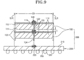
- FIGS. 4 through 9 are cross-sectional views illustrating a method for manufacturing a semiconductor package in accordance with a still another embodiment of the present invention.
- a semiconductor chip 100 is first manufactured.
- a plurality of semiconductor chips 100 are formed on a wafer 160 in the type of a matrix through a semiconductor chip manufacturing process. Scribe lines SL are formed between semiconductor chips 100 such that the semiconductor chips 100 can be parted from the wafer 160 along the scribe lines SL.
- Regions of the wafer 160 in which the semiconductor chips 100 are formed, are defined as chip regions CR, and regions of the wafer 160 , in which the scribe lines SL for partitioning the chip regions CR are formed, are defined as scribe line regions SLR.
- Each of the plurality of semiconductor chips 100 formed on the wafer 160 includes a semiconductor chip body 110 .
- the semiconductor chip body 110 has a first surface 112 and a second surface 114 which faces away from the first surface 112 .
- Bonding pads 116 which are electrically connected with the circuit part (not shown) formed in the semiconductor chip body 110 , are located on the first surface 112 .
- the bonding pads 116 can be arranged in line on the center portion of the first surface 112 of the semiconductor chip body 110 or on the edge portions of the first surface 112 of the semiconductor chip body 110 .
- the bonding pads 116 are arranged, for example, on the center portion of the first surface 112 of the semiconductor chip body 110 .
- through-electrodes 120 are formed in each semiconductor chip body 110 in such a way as to pass through the first and second surfaces 112 and 114 of the semiconductor chip body 110 .
- grooves 121 to be used for forming through-electrodes are defined through the bonding pads 116 formed on the first surface 112 of each semiconductor chip 100 and in portions of the semiconductor chip 100 which correspond to the bonding pads 116 .
- the depth of the grooves 121 is set to be less than the thickness of the semiconductor chip 100 .
- a metal seed layer is formed on the inner surfaces of the grooves 121 to allow through-electrodes to be formed in the grooves 121 through a plating process.
- the metal seed layer is a metal layer which has a small thickness.
- the exemplary metals, which can be used for forming the metal seed layer, can include titanium, nickel and vanadium.
- the through-electrodes 120 having the shape of a column are formed in the grooves 121 through a plating process. Copper can be used for forming the through-electrodes 120 .
- solder members 140 such as solder balls can be formed on the bonding pads 116 which are formed on the first surface 112 of the semiconductor chip body 110 .
- the second surface 114 of the semiconductor chip body 110 is grinded through a grinding process, such that the thickness of the semiconductor chip body 110 measured between the first surface 112 and the second surface 114 decreases from T 1 to T 2 .
- each semiconductor chip body 110 is grinded through the grinding process, warpage or twisting can occur in the wafer 160 having the semiconductor chips 100 .
- the warpage and twisting of the wafer 160 occurs in proportion to the thickness of the semiconductor chip body 110 to be grinded.
- a photoresist film (not shown) is to formed on the entire area of the second surface 114 of the grinded semiconductor chip body 110 .
- the photoresist film can be formed, for example, through a spin coating process.
- the photoresist film applied to the second surface 114 of the grinded semiconductor chip body 110 is patterned through a photo process including a lithography process and a development process, and through this, a photoresist pattern 170 is formed on the second surface 114 of the semiconductor chip body 110 in correspondence with the scribe line regions SLR.
- the second surface 114 of the semiconductor chip body 110 is etched using the photoresist pattern 170 as an etch mask, and thereby, a warpage prevention part 130 , which projects from the second surface 114 , is formed on the second surface 114 of the semiconductor chip body 110 along the scribe line regions SLR.
- the photoresist pattern 170 is removed from the second surface 114 through an ashing process or a stripping process.
- the warpage prevention part 130 is formed along the scribe line regions SLR, and as a result of this, when viewing the wafer 160 from the top, warpage prevention parts 130 define the shape of a lattice. Due to the presence of the warpage prevention parts 130 , the warpage of the wafer 160 and the semiconductor chips 100 formed on the wafer 160 is prevented.
- the plurality of semiconductor chips 100 As the scribe line regions SLR are cut by a sawing machine, the plurality of semiconductor chips 100 , which are formed on the wafer 160 , are individually parted. Although the parted semiconductor chips 100 have a small thickness, they have the warpage prevention parts 130 . Therefore, even though the plurality of semiconductor chips 100 are parted from the wafer 160 , the warpage and twisting of the semiconductor chips 100 is minimized, suppressed or prevented due to the presence of the warpage prevention parts 130 .
- At least two of the semiconductor chips 100 parted from the wafer 160 are stacked, and the stacked semiconductor chips 100 are electrically connected with each other by the solder members 140 .
- At least two stacked semiconductor chips 100 are located on the substrate body 210 of the substrate 200 having the connection pads 220 on which solder members are formed, and the through-electrodes 120 of the semiconductor chip 100 are electrically connected with the solder members formed on the connection pads 220 , whereby the manufacture of a semiconductor package 300 as shown in FIG. 9 is completed.
- the rear surface of the wafer is grinded to reduce the volume of the semiconductor chips, and warpage prevention parts are formed on the rear surface of the grinded wafer, whereby it is possible to minimize, suppress or prevent the wafer or the semiconductor chips formed on the wafer from being warped and twisted.
Abstract
Description
Claims (7)
Priority Applications (1)
| Application Number | Priority Date | Filing Date | Title |
|---|---|---|---|
| US12/848,472 US7989264B2 (en) | 2007-11-30 | 2010-08-02 | Warpage resistant semiconductor package and method for manufacturing the same |
Applications Claiming Priority (4)
| Application Number | Priority Date | Filing Date | Title |
|---|---|---|---|
| KR10-2007-0123758 | 2007-11-30 | ||
| KR1020070123758A KR100963617B1 (en) | 2007-11-30 | 2007-11-30 | Semiconductor package and method of manufacturing thereof |
| US12/044,420 US7795718B2 (en) | 2007-11-30 | 2008-03-07 | Warpage resistant semiconductor package and method for manufacturing the same |
| US12/848,472 US7989264B2 (en) | 2007-11-30 | 2010-08-02 | Warpage resistant semiconductor package and method for manufacturing the same |
Related Parent Applications (1)
| Application Number | Title | Priority Date | Filing Date |
|---|---|---|---|
| US12/044,420 Division US7795718B2 (en) | 2007-11-30 | 2008-03-07 | Warpage resistant semiconductor package and method for manufacturing the same |
Publications (2)
| Publication Number | Publication Date |
|---|---|
| US20100317151A1 US20100317151A1 (en) | 2010-12-16 |
| US7989264B2 true US7989264B2 (en) | 2011-08-02 |
Family
ID=40674886
Family Applications (2)
| Application Number | Title | Priority Date | Filing Date |
|---|---|---|---|
| US12/044,420 Active 2028-12-09 US7795718B2 (en) | 2007-11-30 | 2008-03-07 | Warpage resistant semiconductor package and method for manufacturing the same |
| US12/848,472 Active US7989264B2 (en) | 2007-11-30 | 2010-08-02 | Warpage resistant semiconductor package and method for manufacturing the same |
Family Applications Before (1)
| Application Number | Title | Priority Date | Filing Date |
|---|---|---|---|
| US12/044,420 Active 2028-12-09 US7795718B2 (en) | 2007-11-30 | 2008-03-07 | Warpage resistant semiconductor package and method for manufacturing the same |
Country Status (2)
| Country | Link |
|---|---|
| US (2) | US7795718B2 (en) |
| KR (1) | KR100963617B1 (en) |
Cited By (2)
| Publication number | Priority date | Publication date | Assignee | Title |
|---|---|---|---|---|
| US9721926B2 (en) | 2014-08-27 | 2017-08-01 | Samsung Electronics Co., Ltd. | Semiconductor device having stacked semiconductor chips interconnected via TSV and method of fabricating the same |
| TWI648831B (en) * | 2014-04-14 | 2019-01-21 | 日商瑞薩電子股份有限公司 | Semiconductor device and method of manufacturing same |
Families Citing this family (6)
| Publication number | Priority date | Publication date | Assignee | Title |
|---|---|---|---|---|
| US8153464B2 (en) * | 2005-10-18 | 2012-04-10 | International Rectifier Corporation | Wafer singulation process |
| US7745920B2 (en) * | 2008-06-10 | 2010-06-29 | Micron Technology, Inc. | Packaged microelectronic devices and methods for manufacturing packaged microelectronic devices |
| KR20100048610A (en) * | 2008-10-31 | 2010-05-11 | 삼성전자주식회사 | Semiconductor fackage and forming method of the same |
| KR101144082B1 (en) * | 2012-01-26 | 2012-05-23 | 한국기계연구원 | Semiconductor chip stack package and manufacturing method thereof |
| KR102007259B1 (en) | 2012-09-27 | 2019-08-06 | 삼성전자주식회사 | Semiconductor package and method for manufacturing the same |
| WO2019245809A1 (en) * | 2018-06-21 | 2019-12-26 | Corning Incorporated | Stiffened thin substrates and articles formed therefrom |
Citations (7)
| Publication number | Priority date | Publication date | Assignee | Title |
|---|---|---|---|---|
| KR20020054476A (en) | 2000-12-28 | 2002-07-08 | 윤종용 | Printed circuit board for semiconductor chip package |
| KR20030013737A (en) | 2001-08-09 | 2003-02-15 | 삼성전자주식회사 | Semiconductor package and method for manufacturing the same |
| US20060073637A1 (en) * | 2004-08-31 | 2006-04-06 | Yoshihiko Yokoyama | Method for manufacturing semiconductor device and semiconductor device |
| KR100621438B1 (en) | 2005-08-31 | 2006-09-08 | 삼성전자주식회사 | Stack chip package using photo sensitive polymer and manufacturing method thereof |
| US20070210447A1 (en) | 2006-03-07 | 2007-09-13 | Kinsley Thomas H | Elongated fasteners for securing together electronic components and substrates, semiconductor device assemblies including such fasteners, and accompanying systems and methods |
| KR20070112645A (en) | 2006-05-22 | 2007-11-27 | 삼성전자주식회사 | Semiconductor package having anchor type joining and method of fabricating the same |
| US20080169545A1 (en) | 2007-01-16 | 2008-07-17 | Samsung Electronics Co., Ltd. | Stacked structure of semiconductor devices, semiconductor device package, and methods of fabricating the same |
-
2007
- 2007-11-30 KR KR1020070123758A patent/KR100963617B1/en not_active IP Right Cessation
-
2008
- 2008-03-07 US US12/044,420 patent/US7795718B2/en active Active
-
2010
- 2010-08-02 US US12/848,472 patent/US7989264B2/en active Active
Patent Citations (8)
| Publication number | Priority date | Publication date | Assignee | Title |
|---|---|---|---|---|
| KR20020054476A (en) | 2000-12-28 | 2002-07-08 | 윤종용 | Printed circuit board for semiconductor chip package |
| KR20030013737A (en) | 2001-08-09 | 2003-02-15 | 삼성전자주식회사 | Semiconductor package and method for manufacturing the same |
| US20060073637A1 (en) * | 2004-08-31 | 2006-04-06 | Yoshihiko Yokoyama | Method for manufacturing semiconductor device and semiconductor device |
| KR100621438B1 (en) | 2005-08-31 | 2006-09-08 | 삼성전자주식회사 | Stack chip package using photo sensitive polymer and manufacturing method thereof |
| US20070210447A1 (en) | 2006-03-07 | 2007-09-13 | Kinsley Thomas H | Elongated fasteners for securing together electronic components and substrates, semiconductor device assemblies including such fasteners, and accompanying systems and methods |
| KR20070112645A (en) | 2006-05-22 | 2007-11-27 | 삼성전자주식회사 | Semiconductor package having anchor type joining and method of fabricating the same |
| US20080169545A1 (en) | 2007-01-16 | 2008-07-17 | Samsung Electronics Co., Ltd. | Stacked structure of semiconductor devices, semiconductor device package, and methods of fabricating the same |
| US7588964B2 (en) * | 2007-01-16 | 2009-09-15 | Samsung Electronics Co., Ltd. | Methods of stacking semiconductor devices and methods of fabricating semiconductor device packages using the same |
Non-Patent Citations (2)
| Title |
|---|
| USPTO Notice of Allowance mailed Jun. 1, 2010 for U.S. Appl. No. 12/044,420. |
| USPTO Office Action mailed Feb. 17, 2010 for U.S. Appl. No. 12/044,420. |
Cited By (3)
| Publication number | Priority date | Publication date | Assignee | Title |
|---|---|---|---|---|
| TWI648831B (en) * | 2014-04-14 | 2019-01-21 | 日商瑞薩電子股份有限公司 | Semiconductor device and method of manufacturing same |
| US9721926B2 (en) | 2014-08-27 | 2017-08-01 | Samsung Electronics Co., Ltd. | Semiconductor device having stacked semiconductor chips interconnected via TSV and method of fabricating the same |
| US10020290B2 (en) | 2014-08-27 | 2018-07-10 | Samsung Electronics Co., Ltd. | Semiconductor device having stacked semiconductor chips interconnected via TSV |
Also Published As
| Publication number | Publication date |
|---|---|
| KR20090056553A (en) | 2009-06-03 |
| KR100963617B1 (en) | 2010-06-16 |
| US20100317151A1 (en) | 2010-12-16 |
| US7795718B2 (en) | 2010-09-14 |
| US20090140392A1 (en) | 2009-06-04 |
Similar Documents
| Publication | Publication Date | Title |
|---|---|---|
| US7989264B2 (en) | Warpage resistant semiconductor package and method for manufacturing the same | |
| US10734367B2 (en) | Semiconductor package and method of fabricating the same | |
| US11626393B2 (en) | Semiconductor package and method of fabricating the same | |
| US10224254B2 (en) | Package process method including disposing a die within a recess of a one-piece material | |
| US8198136B2 (en) | Stacked semiconductor package electrically connecting semiconductor chips using outer surfaces thereof and method for manufacturing the same | |
| US7115483B2 (en) | Stacked chip package having upper chip provided with trenches and method of manufacturing the same | |
| US8847369B2 (en) | Packaging structures and methods for semiconductor devices | |
| US20170018493A1 (en) | Semiconductor package and manufacturing method thereof | |
| JP2004039929A (en) | Semiconductor device and method for manufacturing bump of semiconductor chip | |
| KR102506698B1 (en) | Method of fabricating semiconductor package including reinforcement top die | |
| TW201737446A (en) | Semiconductor package with multiple coplanar interposers | |
| US9691661B2 (en) | Low profile IC package | |
| US11289430B2 (en) | Semiconductor package and a method for manufacturing the same | |
| US7638365B2 (en) | Stacked chip package and method for forming the same | |
| US9312175B2 (en) | Surface modified TSV structure and methods thereof | |
| KR100871707B1 (en) | Wafer level package preventing a chipping defect and manufacturing method thereof | |
| CN109712941A (en) | Substrat structure, the semiconductor package comprising substrat structure, and the semiconductor technology of manufacture semiconductor package | |
| US7595255B2 (en) | Method for manufacturing strip level substrate without warpage and method for manufacturing semiconductor package using the same | |
| KR102540829B1 (en) | Semiconductor package, method for semiconductor package and method for re-distribution layer structure | |
| US20110001234A1 (en) | Semiconductor device and fabrication method thereof | |
| US20100148337A1 (en) | Stackable semiconductor package and process to manufacture same | |
| US20220068832A1 (en) | Integrated circuit package structure and method of manufacturing the same | |
| KR100842916B1 (en) | Method for fabricating stack package | |
| TWI501352B (en) | Integrated circuit packaging system with warpage control system and method of manufacture thereof | |
| KR20220133636A (en) | Method for manufacturing semiconductor package |
Legal Events
| Date | Code | Title | Description |
|---|---|---|---|
| STCF | Information on status: patent grant |
Free format text: PATENTED CASE |
|
| FEPP | Fee payment procedure |
Free format text: PAYOR NUMBER ASSIGNED (ORIGINAL EVENT CODE: ASPN); ENTITY STATUS OF PATENT OWNER: LARGE ENTITY |
|
| FPAY | Fee payment |
Year of fee payment: 4 |
|
| MAFP | Maintenance fee payment |
Free format text: PAYMENT OF MAINTENANCE FEE, 8TH YEAR, LARGE ENTITY (ORIGINAL EVENT CODE: M1552); ENTITY STATUS OF PATENT OWNER: LARGE ENTITY Year of fee payment: 8 |
|
| MAFP | Maintenance fee payment |
Free format text: PAYMENT OF MAINTENANCE FEE, 12TH YEAR, LARGE ENTITY (ORIGINAL EVENT CODE: M1553); ENTITY STATUS OF PATENT OWNER: LARGE ENTITY Year of fee payment: 12 |