US7962232B2 - Methods and media for processing a circuit board - Google Patents
Methods and media for processing a circuit board Download PDFInfo
- Publication number
- US7962232B2 US7962232B2 US11/618,549 US61854906A US7962232B2 US 7962232 B2 US7962232 B2 US 7962232B2 US 61854906 A US61854906 A US 61854906A US 7962232 B2 US7962232 B2 US 7962232B2
- Authority
- US
- United States
- Prior art keywords
- circuit board
- land
- width
- terminal
- setting
- Prior art date
- Legal status (The legal status is an assumption and is not a legal conclusion. Google has not performed a legal analysis and makes no representation as to the accuracy of the status listed.)
- Active
Links
Images


Classifications
-
- H—ELECTRICITY
- H05—ELECTRIC TECHNIQUES NOT OTHERWISE PROVIDED FOR
- H05K—PRINTED CIRCUITS; CASINGS OR CONSTRUCTIONAL DETAILS OF ELECTRIC APPARATUS; MANUFACTURE OF ASSEMBLAGES OF ELECTRICAL COMPONENTS
- H05K1/00—Printed circuits
- H05K1/02—Details
- H05K1/11—Printed elements for providing electric connections to or between printed circuits
- H05K1/115—Via connections; Lands around holes or via connections
- H05K1/116—Lands, clearance holes or other lay-out details concerning the surrounding of a via
-
- H—ELECTRICITY
- H05—ELECTRIC TECHNIQUES NOT OTHERWISE PROVIDED FOR
- H05K—PRINTED CIRCUITS; CASINGS OR CONSTRUCTIONAL DETAILS OF ELECTRIC APPARATUS; MANUFACTURE OF ASSEMBLAGES OF ELECTRICAL COMPONENTS
- H05K1/00—Printed circuits
- H05K1/02—Details
- H05K1/0266—Marks, test patterns or identification means
- H05K1/0268—Marks, test patterns or identification means for electrical inspection or testing
-
- H—ELECTRICITY
- H05—ELECTRIC TECHNIQUES NOT OTHERWISE PROVIDED FOR
- H05K—PRINTED CIRCUITS; CASINGS OR CONSTRUCTIONAL DETAILS OF ELECTRIC APPARATUS; MANUFACTURE OF ASSEMBLAGES OF ELECTRICAL COMPONENTS
- H05K2201/00—Indexing scheme relating to printed circuits covered by H05K1/00
- H05K2201/09—Shape and layout
- H05K2201/09209—Shape and layout details of conductors
- H05K2201/09372—Pads and lands
- H05K2201/09381—Shape of non-curved single flat metallic pad, land or exposed part thereof; Shape of electrode of leadless component
-
- H—ELECTRICITY
- H05—ELECTRIC TECHNIQUES NOT OTHERWISE PROVIDED FOR
- H05K—PRINTED CIRCUITS; CASINGS OR CONSTRUCTIONAL DETAILS OF ELECTRIC APPARATUS; MANUFACTURE OF ASSEMBLAGES OF ELECTRICAL COMPONENTS
- H05K2201/00—Indexing scheme relating to printed circuits covered by H05K1/00
- H05K2201/09—Shape and layout
- H05K2201/09209—Shape and layout details of conductors
- H05K2201/09654—Shape and layout details of conductors covering at least two types of conductors provided for in H05K2201/09218 - H05K2201/095
- H05K2201/09727—Varying width along a single conductor; Conductors or pads having different widths
-
- H—ELECTRICITY
- H05—ELECTRIC TECHNIQUES NOT OTHERWISE PROVIDED FOR
- H05K—PRINTED CIRCUITS; CASINGS OR CONSTRUCTIONAL DETAILS OF ELECTRIC APPARATUS; MANUFACTURE OF ASSEMBLAGES OF ELECTRICAL COMPONENTS
- H05K3/00—Apparatus or processes for manufacturing printed circuits
- H05K3/30—Assembling printed circuits with electric components, e.g. with resistor
- H05K3/32—Assembling printed circuits with electric components, e.g. with resistor electrically connecting electric components or wires to printed circuits
- H05K3/34—Assembling printed circuits with electric components, e.g. with resistor electrically connecting electric components or wires to printed circuits by soldering
- H05K3/3452—Solder masks
-
- Y—GENERAL TAGGING OF NEW TECHNOLOGICAL DEVELOPMENTS; GENERAL TAGGING OF CROSS-SECTIONAL TECHNOLOGIES SPANNING OVER SEVERAL SECTIONS OF THE IPC; TECHNICAL SUBJECTS COVERED BY FORMER USPC CROSS-REFERENCE ART COLLECTIONS [XRACs] AND DIGESTS
- Y10—TECHNICAL SUBJECTS COVERED BY FORMER USPC
- Y10T—TECHNICAL SUBJECTS COVERED BY FORMER US CLASSIFICATION
- Y10T29/00—Metal working
- Y10T29/49—Method of mechanical manufacture
- Y10T29/49002—Electrical device making
- Y10T29/49117—Conductor or circuit manufacturing
- Y10T29/49124—On flat or curved insulated base, e.g., printed circuit, etc.
- Y10T29/49155—Manufacturing circuit on or in base
Definitions
- the present disclosure relates generally to information handling systems and, more particularly, to circuit boards.
- An information handling system generally processes compiles, stores, and/or communicates information or data for business, personal, or other purposes thereby allowing users to take advantage of the value of the information.
- information handling systems may also vary regarding what information is handled, how the information is handled, how much information is processed, stored, or communicated, and how quickly and efficiently the information may be processed, stored, or communicated.
- the variations in information handling systems allow for information handling systems to be general or configured for a specific user or specific use such as financial transaction processing, airline reservations, enterprise data storage, or global communications.
- information handling systems may include a variety of hardware and software components that may be configured to process, store, and communicate information and may include one or more computer systems, data storage systems, and networking systems.
- a circuit board is an assembly of layers utilized to mechanically support and/or electrically couple internal components within an information handling system (IHS).
- IHS information handling system
- Alternatives for a circuit board include a printed circuit board (PCB), printed board, printed wiring board (PWB) and etched wiring board. Categories and/or types of circuit boards may include controller boards, daughter cards, expansion cards, motherboards, and network interface cards (NICs).
- the manufacture or fabrication of a lead free circuit board involves the integration of numerous elements and/or materials in a multi-step process.
- a method of processing a circuit board in which the method may provide a circuit board having disposed thereon a conductive pattern whereby the pattern may include a trace terminating at a terminal.
- the method may also include depositing conductive material on the terminal and trace to form a land extending away from the terminal on the trace past a projection line.
- the method may further include applying a soldermask to the circuit board to form a soldermask opening having an opening edge located at and aligned with the projection line, with the opening framing the terminal and a first portion of the land, and to cover a second portion of the land.
- a non-limiting computer-readable medium having executable instructions that when executed by an information handling system may carry out a method of processing a circuit board having disposed thereon a conductive pattern, the pattern including traces terminating at terminals whereby the method may include locating the terminals, identifying terminals meeting criteria to obtain selected terminals and depositing conductive material on the selected terminals to form on each selected terminal a land extending away from the terminal on the trace past a projection line.
- a circuit board which may include a substrate having disposed thereon a conductive pattern, the pattern including a trace terminating at a terminal, a land having a portion positioned on the terminal and extending away from the terminal along the trace.
- the circuit board may further include a soldermask defining a soldermask opening which may frame the terminal and a first portion of the land, and wherein the soldermask covers a second portion of the land.
- FIG. 1 is a schematic diagram depicting a non-limiting example of a portion of a circuit board which may be included within the hardware components of an IHS.
- FIG. 2A is shown a non-limiting example of a circuit board to which a soldermask has been applied covering a portion of a conductive pattern on the circuit board (which covered portion is shown as dashed lines).
- FIG. 2B is shown a non-limiting example of an enlarged isolated portion of a soldermask opening.
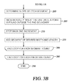
- FIGS. 3A and 3B are collectively a flowchart illustrating a non-limiting method embodiment to deposit conductive material onto a circuit board.
- an embodiment of an Information Handling System may include any instrumentality or aggregate of instrumentalities operable to compute, classify, process, transmit, receive, retrieve, originate, switch, store, display, manifest, detect, record, reproduce handle, or utilize any form of information, intelligence, or data for business, scientific, control, or other purposes.
- an IHS may be a personal computer, a network storage device, or any other suitable device and may vary in size, shape, performance, functionality, and price.
- the IHS may include random access memory (RAM), one or more processing resources such as a central processing unit (CPU) or hardware or software control logic, ROM, and/or other types of nonvolatile memory.
- IHS may include one or more disk drives, one or more network ports for communicating with external devices as well as various input and output (I/O) devices, such as a keyboard, a mouse, and a video display.
- I/O input and output
- the IHS may also include one or more buses operable to transmit data communications between the various hardware components.
- FIG. 1 is a schematic diagram depicting a non-limiting example of a portion of a circuit board 50 which may be included within the hardware components of an IHS.
- the circuit board 50 may comprise a substrate 55 onto which a conductive pattern 61 comprising conductive traces 65 is disposed.
- the substrate 55 may consist of any suitable non-conductive material, non-limiting examples of which include composites, fiberglass, epoxy, paper, ceramic and/or plastic.
- the entire substrate 55 or only its surface to which the conductive pattern 61 is disposed may be formed of the insulating material.
- a circuit board 50 may comprise at least one layer of conductive pattern 61 separated and supported by substrates.
- the conductive pattern 61 disposed on the circuit board 50 may comprise a trace 65 which may comprise a number of terminations at pads 70 or vias 71 collectively referred to herein as “terminals.”
- Traces 65 also called tracks, circuit lines or wires, interconnect electrical components (e.g. resistors, diodes, transistors, etc.) that later in the manufacturing process will be placed on one or both surfaces of the circuit board 50 .
- the traces 65 may be etched from conductive material onto the substrate 55 .
- the pads 70 may be areas of the circuit board 50 for connection and attachment of electronic components whereas vias 71 are holes or apertures in the circuit board 50 for the purpose of layer-to-layer interconnection.
- Projection lines 22 are not part of circuit board 50 but are provided in FIG. 1 to illustrate positioning of soldermask openings that will be formed in the application of a soldermask (e.g., coating or inert coating). Specifically, the defining edge 29 as seen in FIG. 2A of the soldermask opening 27 that will be formed upon application of a soldermask is located at and aligned with projection line 22 .
- conductive material may be added to certain trace terminals depending upon selection criteria. This conductive material is added forming a land 68 starting from inside pad 70 or via 71 and extending away from pad 70 or via 71 along trace 65 past the projection line 22 . In one non-limiting embodiment, this conductive material is added to all pads on a circuit board, and to vias which are testable and which are not be covered by soldermask.
- a circuit board may comprise an assembly of the layers previously described. However, for the purpose of this disclosure, it is also understood that a circuit board exists at any stage of a multi-step assembly process provided that at least a substrate layer is present.
- FIG. 2A there is shown circuit board 50 to which a soldermask 25 has been applied covering a portion of the conductive pattern 61 (which covered portion is shown as dashed lines).
- FIG. 2B is an enlarged isolated portion of one soldermask opening 27 from FIG. 2A .
- the soldermask 25 defines a number of soldermask openings 27 , each of which may outline a corresponding pad 70 or via 71 .
- the soldermask opening 27 may also define an opening edge 29 , which follows the contour of and is aligned with the projection line 22 .
- Added land 68 spans from inside pad 70 or via 71 and extends away from the pad 70 or via 71 along the trace 65 past and under the opening edge 29 , terminating beneath the soldermask 25 .
- the pad boundary 30 frames the terminals and may be found on either a pad 70 or via 71 .
- FIGS. 3A and 3B are collectively a flowchart illustrating a non-limiting embodiment of a method to deposit conductive material onto a circuit board.
- Various method embodiments of this method may include one or more of the steps from FIGS. 3A and 3B carried out in any order as desired. It should be understood that any embodiments of these various methods or computer implemented methods may be carried out by an information handling system (IHS).
- IHS information handling system
- the IHS may accept the commands initiated by a user.
- Step 205 includes setting the top and bottom layers visible.
- One non-limiting embodiment of this disclosure may provide for the deposit of conductive material to form a land when the land is on a top or bottom layer of the circuit board.
- the IHS is instructed to set the find filter to identify terminals, or “pads” and “vias”.
- the method may prompt a user to define a selection box to set the criteria for selection.
- only testable vias may be selected. As another non-limiting example, all pads may be selected and only vias that are testable and not to be covered by soldermask may be selected.
- a loop may be executed for each pad or via found.
- a check is made for “etch” endpoints within the pad boundary.
- a determination is made at step 235 for a set of endpoints for each segment with at least one endpoint in a pad boundary.
- Step 240 begins a loop for each segment found.
- an assessment is made as to whether both endpoints fall within the pad boundary. If the endpoints fall within the boundary, then at step 250 , the etch segment is set to the desired width.
- step 255 is to locate an endpoint that is within the pad boundary.
- step 260 is to determine slope of the etch segment.
- Step 265 is to incrementally “walk” the line until a point is found outside the pad boundary, thus establishing the size of land to deposit.
- a provision is then made to step back one increment at step 270 .
- step 275 a segment of conductive material of desired width and length is added. This is continued until a loop is completed for each pad and/or via found with the various loops ending at steps 280 , 285 and 290 .
- additional steps may be added before, after or between any of the steps shown in FIGS. 3A and 3B .
- Some of the various embodiments of the present disclosure may provide solutions to allow processing of circuit boards in a lead free manufacturing process.
- consideration is given to the size of a land.
- only lands under a certain size need to be considered.
- only pads and vias that meet the conditions are affected.
- addition of conductive material is made of a length of a specific size land from the center of the pad that extends along the land path past the soldermask opening. This approach may reduce or eliminate the spacing problems that can inhibit the adding of fillets to the pads and vias in highly constrained and dense printed circuit board designs.
- Such storage media may take various forms such as cards, tapes, magnetic disks (e.g., floppy disk or hard drive) and optical disks (e.g., compact disk read only memory (“CD-ROM”) or digital versatile disc (“DVD”)). It should be understood that the given implementations are illustrative only and shall not limit the present disclosure.
Abstract
Description
Claims (20)
Priority Applications (1)
| Application Number | Priority Date | Filing Date | Title |
|---|---|---|---|
| US11/618,549 US7962232B2 (en) | 2006-10-01 | 2006-12-29 | Methods and media for processing a circuit board |
Applications Claiming Priority (2)
| Application Number | Priority Date | Filing Date | Title |
|---|---|---|---|
| US53765006A | 2006-10-01 | 2006-10-01 | |
| US11/618,549 US7962232B2 (en) | 2006-10-01 | 2006-12-29 | Methods and media for processing a circuit board |
Related Parent Applications (1)
| Application Number | Title | Priority Date | Filing Date |
|---|---|---|---|
| US53765006A Continuation | 2006-10-01 | 2006-10-01 |
Publications (2)
| Publication Number | Publication Date |
|---|---|
| US20080185170A1 US20080185170A1 (en) | 2008-08-07 |
| US7962232B2 true US7962232B2 (en) | 2011-06-14 |
Family
ID=39675189
Family Applications (1)
| Application Number | Title | Priority Date | Filing Date |
|---|---|---|---|
| US11/618,549 Active US7962232B2 (en) | 2006-10-01 | 2006-12-29 | Methods and media for processing a circuit board |
Country Status (1)
| Country | Link |
|---|---|
| US (1) | US7962232B2 (en) |
Citations (25)
| Publication number | Priority date | Publication date | Assignee | Title |
|---|---|---|---|---|
| US4752887A (en) * | 1985-03-01 | 1988-06-21 | Nec Corporation | Routing method for use in wiring design |
| US5542600A (en) * | 1991-11-07 | 1996-08-06 | Omron Corporation | Automatic soldering apparatus, apparatus and method for teaching same, soldering inspection apparatus and method, and apparatus and method for automatically correcting soldering |
| US5800859A (en) | 1994-12-12 | 1998-09-01 | Price; Andrew David | Copper coating of printed circuit boards |
| US6086627A (en) * | 1998-01-29 | 2000-07-11 | International Business Machines Corporation | Method of automated ESD protection level verification |
| US6141643A (en) * | 1998-11-25 | 2000-10-31 | Harmon; Steve | Data input glove having conductive finger pads and thumb pad, and uses therefor |
| US6180215B1 (en) | 1999-07-14 | 2001-01-30 | Intel Corporation | Multilayer printed circuit board and manufacturing method thereof |
| US6339197B1 (en) * | 1999-05-27 | 2002-01-15 | Hoya Corporation | Multilayer printed circuit board and the manufacturing method |
| US6446239B1 (en) * | 1998-03-10 | 2002-09-03 | Monterey Design Systems, Inc. | Method and apparatus for optimizing electronic design |
| US20020166696A1 (en) * | 2001-05-10 | 2002-11-14 | International Business Machines Corporation | Land grid array (LGA) pad repair structure and method |
| US6643839B1 (en) * | 1999-07-08 | 2003-11-04 | International Business Machines Corporation | Determining an optimum wiring pattern and component placement scheme for a printed wiring board |
| US6651324B1 (en) | 2000-11-06 | 2003-11-25 | Viasystems Group, Inc. | Process for manufacture of printed circuit boards with thick copper power circuitry and thin copper signal circuitry on the same layer |
| US6664483B2 (en) * | 2001-05-15 | 2003-12-16 | Intel Corporation | Electronic package with high density interconnect and associated methods |
| US6665854B2 (en) * | 2000-12-04 | 2003-12-16 | Matsushita Electric Industrial Co., Ltd. | Method and apparatus of checking mount quality of circuit board |
| US20040040008A1 (en) * | 2002-08-22 | 2004-02-26 | Cherif Ahrikencheikh | Determining via placement in the printed circuit board of a wireless test fixture |
| US20040163054A1 (en) * | 2003-02-19 | 2004-08-19 | Frank Mark D. | System and method for evaluating vias per pad in a package design |
| US6938227B2 (en) * | 2002-08-08 | 2005-08-30 | Fry's Metals, Inc. | System and method for modifying electronic design data |
| US20060040532A1 (en) * | 2004-08-18 | 2006-02-23 | Fujitsu Limited | Method of designing circuit board |
| US20070028202A1 (en) * | 2005-07-27 | 2007-02-01 | Fujitsu Limited | Method and apparatus for generating design information, and computer product |
| US7199478B2 (en) * | 2001-07-11 | 2007-04-03 | Samsung Electronics Co., Ltd. | Printed circuit board having an improved land structure |
| US20070148816A1 (en) * | 2005-12-22 | 2007-06-28 | International Business Machines Corporation | Attachment of a QFN to a PCB |
| US7353480B1 (en) * | 2004-12-07 | 2008-04-01 | Nvidia Corporation | Apparatus, system, and method for designing via pads having extended contours |
| US7411221B2 (en) * | 2005-08-03 | 2008-08-12 | Samsung Electro-Mechanics Co., Ltd. | Light emitting device having protection element and method of manufacturing the light emitting device |
| US7496878B2 (en) * | 2004-04-13 | 2009-02-24 | Shinko Electrics Industries Co., Ltd. | Automatic wiring method and apparatus for semiconductor package and automatic identifying method and apparatus for semiconductor package |
| US7544304B2 (en) * | 2006-07-11 | 2009-06-09 | Electro Scientific Industries, Inc. | Process and system for quality management and analysis of via drilling |
| US7603642B2 (en) * | 2006-09-27 | 2009-10-13 | Cadence Design Systems, Inc. | Placer with wires for RF and analog design |
-
2006
- 2006-12-29 US US11/618,549 patent/US7962232B2/en active Active
Patent Citations (30)
| Publication number | Priority date | Publication date | Assignee | Title |
|---|---|---|---|---|
| US4752887A (en) * | 1985-03-01 | 1988-06-21 | Nec Corporation | Routing method for use in wiring design |
| US5542600A (en) * | 1991-11-07 | 1996-08-06 | Omron Corporation | Automatic soldering apparatus, apparatus and method for teaching same, soldering inspection apparatus and method, and apparatus and method for automatically correcting soldering |
| US5800859A (en) | 1994-12-12 | 1998-09-01 | Price; Andrew David | Copper coating of printed circuit boards |
| US6086627A (en) * | 1998-01-29 | 2000-07-11 | International Business Machines Corporation | Method of automated ESD protection level verification |
| US6446239B1 (en) * | 1998-03-10 | 2002-09-03 | Monterey Design Systems, Inc. | Method and apparatus for optimizing electronic design |
| US6141643A (en) * | 1998-11-25 | 2000-10-31 | Harmon; Steve | Data input glove having conductive finger pads and thumb pad, and uses therefor |
| US20060000640A1 (en) * | 1999-05-27 | 2006-01-05 | Hoya Corporation | Multilayer printed wiring board and a process of producing same |
| US6339197B1 (en) * | 1999-05-27 | 2002-01-15 | Hoya Corporation | Multilayer printed circuit board and the manufacturing method |
| US6643839B1 (en) * | 1999-07-08 | 2003-11-04 | International Business Machines Corporation | Determining an optimum wiring pattern and component placement scheme for a printed wiring board |
| US6180215B1 (en) | 1999-07-14 | 2001-01-30 | Intel Corporation | Multilayer printed circuit board and manufacturing method thereof |
| US20040168314A1 (en) | 2000-11-06 | 2004-09-02 | Giuseppe Pedretti | Process for manufacture of printed circuit boards with thick copper power circuitry and thin copper signal circuitry on the same layer |
| US6651324B1 (en) | 2000-11-06 | 2003-11-25 | Viasystems Group, Inc. | Process for manufacture of printed circuit boards with thick copper power circuitry and thin copper signal circuitry on the same layer |
| US6665854B2 (en) * | 2000-12-04 | 2003-12-16 | Matsushita Electric Industrial Co., Ltd. | Method and apparatus of checking mount quality of circuit board |
| US20020166696A1 (en) * | 2001-05-10 | 2002-11-14 | International Business Machines Corporation | Land grid array (LGA) pad repair structure and method |
| US6664483B2 (en) * | 2001-05-15 | 2003-12-16 | Intel Corporation | Electronic package with high density interconnect and associated methods |
| US7199478B2 (en) * | 2001-07-11 | 2007-04-03 | Samsung Electronics Co., Ltd. | Printed circuit board having an improved land structure |
| US6938227B2 (en) * | 2002-08-08 | 2005-08-30 | Fry's Metals, Inc. | System and method for modifying electronic design data |
| US20040040008A1 (en) * | 2002-08-22 | 2004-02-26 | Cherif Ahrikencheikh | Determining via placement in the printed circuit board of a wireless test fixture |
| US6839885B2 (en) * | 2002-08-22 | 2005-01-04 | Agilent Technologies, Inc. | Determining via placement in the printed circuit board of a wireless test fixture |
| US20040163054A1 (en) * | 2003-02-19 | 2004-08-19 | Frank Mark D. | System and method for evaluating vias per pad in a package design |
| US6907589B2 (en) * | 2003-02-19 | 2005-06-14 | Hewlett-Packard Development Company, L.P. | System and method for evaluating vias per pad in a package design |
| US7496878B2 (en) * | 2004-04-13 | 2009-02-24 | Shinko Electrics Industries Co., Ltd. | Automatic wiring method and apparatus for semiconductor package and automatic identifying method and apparatus for semiconductor package |
| US20060040532A1 (en) * | 2004-08-18 | 2006-02-23 | Fujitsu Limited | Method of designing circuit board |
| US7251801B2 (en) * | 2004-08-18 | 2007-07-31 | Fujitsu Limited | Method of designing circuit board |
| US7353480B1 (en) * | 2004-12-07 | 2008-04-01 | Nvidia Corporation | Apparatus, system, and method for designing via pads having extended contours |
| US20070028202A1 (en) * | 2005-07-27 | 2007-02-01 | Fujitsu Limited | Method and apparatus for generating design information, and computer product |
| US7411221B2 (en) * | 2005-08-03 | 2008-08-12 | Samsung Electro-Mechanics Co., Ltd. | Light emitting device having protection element and method of manufacturing the light emitting device |
| US20070148816A1 (en) * | 2005-12-22 | 2007-06-28 | International Business Machines Corporation | Attachment of a QFN to a PCB |
| US7544304B2 (en) * | 2006-07-11 | 2009-06-09 | Electro Scientific Industries, Inc. | Process and system for quality management and analysis of via drilling |
| US7603642B2 (en) * | 2006-09-27 | 2009-10-13 | Cadence Design Systems, Inc. | Placer with wires for RF and analog design |
Non-Patent Citations (3)
| Title |
|---|
| 2008 Signal Integrity Training Classes; 2 pages. * |
| Land Repair, Film Adhesive Method; 4 pages. * |
| PCB Land Pattern Design and Surface Mount Guidelines for QFN Packages; 9 pages. * |
Also Published As
| Publication number | Publication date |
|---|---|
| US20080185170A1 (en) | 2008-08-07 |
Similar Documents
| Publication | Publication Date | Title |
|---|---|---|
| US6774486B2 (en) | Circuit boards containing vias and methods for producing same | |
| JP2842378B2 (en) | High-density mounting structure for electronic circuit boards | |
| US10051733B2 (en) | Printed circuit board with coextensive electrical connectors and contact pad areas | |
| KR100776248B1 (en) | Manufacturing method of printed circuit board | |
| US8011086B2 (en) | Method of manufacturing a component-embedded printed circuit board | |
| US8377815B2 (en) | Manufacturing method of a semiconductor load board | |
| US20080113502A1 (en) | Electronic device | |
| EP1592290A1 (en) | Wired circuit board and production method thereof | |
| US20130213695A1 (en) | Method of manufacturing flying tail type rigid-flexible printed circuit board and flying tail type rigid-flexible printed circuit board manufactured by the same | |
| US8266792B2 (en) | Method of manufacturing a printed circuit board with an embedded electronic component | |
| KR101831643B1 (en) | Package substrate comprising surface interconnect and cavity comprising electroless fill | |
| JP2009094361A (en) | Cof board | |
| JP2001320150A (en) | Wiring board by stamper and manufacturing method thereof | |
| CN101090074A (en) | Printed circuit board for package of electronic components and manufacturing method thereof | |
| CN107787122B (en) | Circuit board line compensation method and device | |
| JPH10125818A (en) | Substrate for semiconductor device, semiconductor device and manufacture thereof | |
| JPH05183259A (en) | Manufacture of high density printed wiring board | |
| JP2005311289A (en) | Circuit connecting structure and manufacturing method of the same | |
| US7962232B2 (en) | Methods and media for processing a circuit board | |
| JP2003045917A (en) | Tape carrier for semiconductor device and its manufacturing method | |
| US7383630B2 (en) | Method for making a circuit plate | |
| JP2003068803A (en) | Tape carrier for semiconductor device and semiconductor device using the same | |
| JP2004281608A (en) | Method for manufacturing circuit substrate | |
| TW200410384A (en) | Optimum power and ground bump pad and bump patterns for flip chip packaging | |
| JP2004274071A (en) | Substrate for semiconductor apparatus, semiconductor apparatus, and manufacturing method for them |
Legal Events
| Date | Code | Title | Description |
|---|---|---|---|
| AS | Assignment |
Owner name: DELL PRODUCTS L.P., TEXAS Free format text: ASSIGNMENT OF ASSIGNORS INTEREST;ASSIGNORS:WILSON, MICHAEL F.;WISEMAN, JOE;REEL/FRAME:025649/0034 Effective date: 20060928 |
|
| STCF | Information on status: patent grant |
Free format text: PATENTED CASE |
|
| AS | Assignment |
Owner name: BANK OF NEW YORK MELLON TRUST COMPANY, N.A., AS FIRST LIEN COLLATERAL AGENT, TEXAS Free format text: PATENT SECURITY AGREEMENT (NOTES);ASSIGNORS:APPASSURE SOFTWARE, INC.;ASAP SOFTWARE EXPRESS, INC.;BOOMI, INC.;AND OTHERS;REEL/FRAME:031897/0348 Effective date: 20131029 Owner name: BANK OF AMERICA, N.A., AS ADMINISTRATIVE AGENT, TEXAS Free format text: PATENT SECURITY AGREEMENT (ABL);ASSIGNORS:DELL INC.;APPASSURE SOFTWARE, INC.;ASAP SOFTWARE EXPRESS, INC.;AND OTHERS;REEL/FRAME:031898/0001 Effective date: 20131029 Owner name: BANK OF AMERICA, N.A., AS COLLATERAL AGENT, NORTH CAROLINA Free format text: PATENT SECURITY AGREEMENT (TERM LOAN);ASSIGNORS:DELL INC.;APPASSURE SOFTWARE, INC.;ASAP SOFTWARE EXPRESS, INC.;AND OTHERS;REEL/FRAME:031899/0261 Effective date: 20131029 Owner name: BANK OF NEW YORK MELLON TRUST COMPANY, N.A., AS FI Free format text: PATENT SECURITY AGREEMENT (NOTES);ASSIGNORS:APPASSURE SOFTWARE, INC.;ASAP SOFTWARE EXPRESS, INC.;BOOMI, INC.;AND OTHERS;REEL/FRAME:031897/0348 Effective date: 20131029 Owner name: BANK OF AMERICA, N.A., AS COLLATERAL AGENT, NORTH Free format text: PATENT SECURITY AGREEMENT (TERM LOAN);ASSIGNORS:DELL INC.;APPASSURE SOFTWARE, INC.;ASAP SOFTWARE EXPRESS, INC.;AND OTHERS;REEL/FRAME:031899/0261 Effective date: 20131029 Owner name: BANK OF AMERICA, N.A., AS ADMINISTRATIVE AGENT, TE Free format text: PATENT SECURITY AGREEMENT (ABL);ASSIGNORS:DELL INC.;APPASSURE SOFTWARE, INC.;ASAP SOFTWARE EXPRESS, INC.;AND OTHERS;REEL/FRAME:031898/0001 Effective date: 20131029 |
|
| FPAY | Fee payment |
Year of fee payment: 4 |
|
| AS | Assignment |
Owner name: DELL MARKETING L.P., TEXAS Free format text: RELEASE BY SECURED PARTY;ASSIGNOR:BANK OF AMERICA, N.A., AS ADMINISTRATIVE AGENT;REEL/FRAME:040065/0216 Effective date: 20160907 Owner name: SECUREWORKS, INC., GEORGIA Free format text: RELEASE BY SECURED PARTY;ASSIGNOR:BANK OF AMERICA, N.A., AS ADMINISTRATIVE AGENT;REEL/FRAME:040065/0216 Effective date: 20160907 Owner name: DELL SOFTWARE INC., CALIFORNIA Free format text: RELEASE BY SECURED PARTY;ASSIGNOR:BANK OF AMERICA, N.A., AS ADMINISTRATIVE AGENT;REEL/FRAME:040065/0216 Effective date: 20160907 Owner name: APPASSURE SOFTWARE, INC., VIRGINIA Free format text: RELEASE BY SECURED PARTY;ASSIGNOR:BANK OF AMERICA, N.A., AS ADMINISTRATIVE AGENT;REEL/FRAME:040065/0216 Effective date: 20160907 Owner name: DELL PRODUCTS L.P., TEXAS Free format text: RELEASE BY SECURED PARTY;ASSIGNOR:BANK OF AMERICA, N.A., AS ADMINISTRATIVE AGENT;REEL/FRAME:040065/0216 Effective date: 20160907 Owner name: DELL INC., TEXAS Free format text: RELEASE BY SECURED PARTY;ASSIGNOR:BANK OF AMERICA, N.A., AS ADMINISTRATIVE AGENT;REEL/FRAME:040065/0216 Effective date: 20160907 Owner name: CREDANT TECHNOLOGIES, INC., TEXAS Free format text: RELEASE BY SECURED PARTY;ASSIGNOR:BANK OF AMERICA, N.A., AS ADMINISTRATIVE AGENT;REEL/FRAME:040065/0216 Effective date: 20160907 Owner name: COMPELLANT TECHNOLOGIES, INC., MINNESOTA Free format text: RELEASE BY SECURED PARTY;ASSIGNOR:BANK OF AMERICA, N.A., AS ADMINISTRATIVE AGENT;REEL/FRAME:040065/0216 Effective date: 20160907 Owner name: FORCE10 NETWORKS, INC., CALIFORNIA Free format text: RELEASE BY SECURED PARTY;ASSIGNOR:BANK OF AMERICA, N.A., AS ADMINISTRATIVE AGENT;REEL/FRAME:040065/0216 Effective date: 20160907 Owner name: DELL USA L.P., TEXAS Free format text: RELEASE BY SECURED PARTY;ASSIGNOR:BANK OF AMERICA, N.A., AS ADMINISTRATIVE AGENT;REEL/FRAME:040065/0216 Effective date: 20160907 Owner name: PEROT SYSTEMS CORPORATION, TEXAS Free format text: RELEASE BY SECURED PARTY;ASSIGNOR:BANK OF AMERICA, N.A., AS ADMINISTRATIVE AGENT;REEL/FRAME:040065/0216 Effective date: 20160907 Owner name: WYSE TECHNOLOGY L.L.C., CALIFORNIA Free format text: RELEASE BY SECURED PARTY;ASSIGNOR:BANK OF AMERICA, N.A., AS ADMINISTRATIVE AGENT;REEL/FRAME:040065/0216 Effective date: 20160907 Owner name: ASAP SOFTWARE EXPRESS, INC., ILLINOIS Free format text: RELEASE BY SECURED PARTY;ASSIGNOR:BANK OF AMERICA, N.A., AS ADMINISTRATIVE AGENT;REEL/FRAME:040065/0216 Effective date: 20160907 |
|
| AS | Assignment |
Owner name: APPASSURE SOFTWARE, INC., VIRGINIA Free format text: RELEASE BY SECURED PARTY;ASSIGNOR:BANK OF AMERICA, N.A., AS COLLATERAL AGENT;REEL/FRAME:040040/0001 Effective date: 20160907 Owner name: WYSE TECHNOLOGY L.L.C., CALIFORNIA Free format text: RELEASE BY SECURED PARTY;ASSIGNOR:BANK OF AMERICA, N.A., AS COLLATERAL AGENT;REEL/FRAME:040040/0001 Effective date: 20160907 Owner name: FORCE10 NETWORKS, INC., CALIFORNIA Free format text: RELEASE BY SECURED PARTY;ASSIGNOR:BANK OF AMERICA, N.A., AS COLLATERAL AGENT;REEL/FRAME:040040/0001 Effective date: 20160907 Owner name: DELL MARKETING L.P., TEXAS Free format text: RELEASE BY SECURED PARTY;ASSIGNOR:BANK OF AMERICA, N.A., AS COLLATERAL AGENT;REEL/FRAME:040040/0001 Effective date: 20160907 Owner name: SECUREWORKS, INC., GEORGIA Free format text: RELEASE BY SECURED PARTY;ASSIGNOR:BANK OF AMERICA, N.A., AS COLLATERAL AGENT;REEL/FRAME:040040/0001 Effective date: 20160907 Owner name: PEROT SYSTEMS CORPORATION, TEXAS Free format text: RELEASE BY SECURED PARTY;ASSIGNOR:BANK OF AMERICA, N.A., AS COLLATERAL AGENT;REEL/FRAME:040040/0001 Effective date: 20160907 Owner name: DELL SOFTWARE INC., CALIFORNIA Free format text: RELEASE BY SECURED PARTY;ASSIGNOR:BANK OF AMERICA, N.A., AS COLLATERAL AGENT;REEL/FRAME:040040/0001 Effective date: 20160907 Owner name: DELL PRODUCTS L.P., TEXAS Free format text: RELEASE BY SECURED PARTY;ASSIGNOR:BANK OF AMERICA, N.A., AS COLLATERAL AGENT;REEL/FRAME:040040/0001 Effective date: 20160907 Owner name: DELL USA L.P., TEXAS Free format text: RELEASE BY SECURED PARTY;ASSIGNOR:BANK OF AMERICA, N.A., AS COLLATERAL AGENT;REEL/FRAME:040040/0001 Effective date: 20160907 Owner name: DELL INC., TEXAS Free format text: RELEASE BY SECURED PARTY;ASSIGNOR:BANK OF AMERICA, N.A., AS COLLATERAL AGENT;REEL/FRAME:040040/0001 Effective date: 20160907 Owner name: ASAP SOFTWARE EXPRESS, INC., ILLINOIS Free format text: RELEASE BY SECURED PARTY;ASSIGNOR:BANK OF AMERICA, N.A., AS COLLATERAL AGENT;REEL/FRAME:040040/0001 Effective date: 20160907 Owner name: CREDANT TECHNOLOGIES, INC., TEXAS Free format text: RELEASE BY SECURED PARTY;ASSIGNOR:BANK OF AMERICA, N.A., AS COLLATERAL AGENT;REEL/FRAME:040040/0001 Effective date: 20160907 Owner name: COMPELLENT TECHNOLOGIES, INC., MINNESOTA Free format text: RELEASE BY SECURED PARTY;ASSIGNOR:BANK OF AMERICA, N.A., AS COLLATERAL AGENT;REEL/FRAME:040040/0001 Effective date: 20160907 Owner name: DELL SOFTWARE INC., CALIFORNIA Free format text: RELEASE BY SECURED PARTY;ASSIGNOR:BANK OF NEW YORK MELLON TRUST COMPANY, N.A., AS COLLATERAL AGENT;REEL/FRAME:040065/0618 Effective date: 20160907 Owner name: ASAP SOFTWARE EXPRESS, INC., ILLINOIS Free format text: RELEASE BY SECURED PARTY;ASSIGNOR:BANK OF NEW YORK MELLON TRUST COMPANY, N.A., AS COLLATERAL AGENT;REEL/FRAME:040065/0618 Effective date: 20160907 Owner name: WYSE TECHNOLOGY L.L.C., CALIFORNIA Free format text: RELEASE BY SECURED PARTY;ASSIGNOR:BANK OF NEW YORK MELLON TRUST COMPANY, N.A., AS COLLATERAL AGENT;REEL/FRAME:040065/0618 Effective date: 20160907 Owner name: FORCE10 NETWORKS, INC., CALIFORNIA Free format text: RELEASE BY SECURED PARTY;ASSIGNOR:BANK OF NEW YORK MELLON TRUST COMPANY, N.A., AS COLLATERAL AGENT;REEL/FRAME:040065/0618 Effective date: 20160907 Owner name: CREDANT TECHNOLOGIES, INC., TEXAS Free format text: RELEASE BY SECURED PARTY;ASSIGNOR:BANK OF NEW YORK MELLON TRUST COMPANY, N.A., AS COLLATERAL AGENT;REEL/FRAME:040065/0618 Effective date: 20160907 Owner name: SECUREWORKS, INC., GEORGIA Free format text: RELEASE BY SECURED PARTY;ASSIGNOR:BANK OF NEW YORK MELLON TRUST COMPANY, N.A., AS COLLATERAL AGENT;REEL/FRAME:040065/0618 Effective date: 20160907 Owner name: APPASSURE SOFTWARE, INC., VIRGINIA Free format text: RELEASE BY SECURED PARTY;ASSIGNOR:BANK OF NEW YORK MELLON TRUST COMPANY, N.A., AS COLLATERAL AGENT;REEL/FRAME:040065/0618 Effective date: 20160907 Owner name: PEROT SYSTEMS CORPORATION, TEXAS Free format text: RELEASE BY SECURED PARTY;ASSIGNOR:BANK OF NEW YORK MELLON TRUST COMPANY, N.A., AS COLLATERAL AGENT;REEL/FRAME:040065/0618 Effective date: 20160907 Owner name: DELL INC., TEXAS Free format text: RELEASE BY SECURED PARTY;ASSIGNOR:BANK OF NEW YORK MELLON TRUST COMPANY, N.A., AS COLLATERAL AGENT;REEL/FRAME:040065/0618 Effective date: 20160907 Owner name: DELL MARKETING L.P., TEXAS Free format text: RELEASE BY SECURED PARTY;ASSIGNOR:BANK OF NEW YORK MELLON TRUST COMPANY, N.A., AS COLLATERAL AGENT;REEL/FRAME:040065/0618 Effective date: 20160907 Owner name: DELL USA L.P., TEXAS Free format text: RELEASE BY SECURED PARTY;ASSIGNOR:BANK OF NEW YORK MELLON TRUST COMPANY, N.A., AS COLLATERAL AGENT;REEL/FRAME:040065/0618 Effective date: 20160907 Owner name: DELL PRODUCTS L.P., TEXAS Free format text: RELEASE BY SECURED PARTY;ASSIGNOR:BANK OF NEW YORK MELLON TRUST COMPANY, N.A., AS COLLATERAL AGENT;REEL/FRAME:040065/0618 Effective date: 20160907 Owner name: COMPELLENT TECHNOLOGIES, INC., MINNESOTA Free format text: RELEASE BY SECURED PARTY;ASSIGNOR:BANK OF NEW YORK MELLON TRUST COMPANY, N.A., AS COLLATERAL AGENT;REEL/FRAME:040065/0618 Effective date: 20160907 |
|
| AS | Assignment |
Owner name: CREDIT SUISSE AG, CAYMAN ISLANDS BRANCH, AS COLLATERAL AGENT, NORTH CAROLINA Free format text: SECURITY AGREEMENT;ASSIGNORS:ASAP SOFTWARE EXPRESS, INC.;AVENTAIL LLC;CREDANT TECHNOLOGIES, INC.;AND OTHERS;REEL/FRAME:040134/0001 Effective date: 20160907 Owner name: THE BANK OF NEW YORK MELLON TRUST COMPANY, N.A., AS NOTES COLLATERAL AGENT, TEXAS Free format text: SECURITY AGREEMENT;ASSIGNORS:ASAP SOFTWARE EXPRESS, INC.;AVENTAIL LLC;CREDANT TECHNOLOGIES, INC.;AND OTHERS;REEL/FRAME:040136/0001 Effective date: 20160907 Owner name: CREDIT SUISSE AG, CAYMAN ISLANDS BRANCH, AS COLLAT Free format text: SECURITY AGREEMENT;ASSIGNORS:ASAP SOFTWARE EXPRESS, INC.;AVENTAIL LLC;CREDANT TECHNOLOGIES, INC.;AND OTHERS;REEL/FRAME:040134/0001 Effective date: 20160907 Owner name: THE BANK OF NEW YORK MELLON TRUST COMPANY, N.A., A Free format text: SECURITY AGREEMENT;ASSIGNORS:ASAP SOFTWARE EXPRESS, INC.;AVENTAIL LLC;CREDANT TECHNOLOGIES, INC.;AND OTHERS;REEL/FRAME:040136/0001 Effective date: 20160907 |
|
| MAFP | Maintenance fee payment |
Free format text: PAYMENT OF MAINTENANCE FEE, 8TH YEAR, LARGE ENTITY (ORIGINAL EVENT CODE: M1552); ENTITY STATUS OF PATENT OWNER: LARGE ENTITY Year of fee payment: 8 |
|
| AS | Assignment |
Owner name: THE BANK OF NEW YORK MELLON TRUST COMPANY, N.A., T Free format text: SECURITY AGREEMENT;ASSIGNORS:CREDANT TECHNOLOGIES, INC.;DELL INTERNATIONAL L.L.C.;DELL MARKETING L.P.;AND OTHERS;REEL/FRAME:049452/0223 Effective date: 20190320 Owner name: THE BANK OF NEW YORK MELLON TRUST COMPANY, N.A., TEXAS Free format text: SECURITY AGREEMENT;ASSIGNORS:CREDANT TECHNOLOGIES, INC.;DELL INTERNATIONAL L.L.C.;DELL MARKETING L.P.;AND OTHERS;REEL/FRAME:049452/0223 Effective date: 20190320 |
|
| AS | Assignment |
Owner name: THE BANK OF NEW YORK MELLON TRUST COMPANY, N.A., TEXAS Free format text: SECURITY AGREEMENT;ASSIGNORS:CREDANT TECHNOLOGIES INC.;DELL INTERNATIONAL L.L.C.;DELL MARKETING L.P.;AND OTHERS;REEL/FRAME:053546/0001 Effective date: 20200409 |
|
| AS | Assignment |
Owner name: WYSE TECHNOLOGY L.L.C., CALIFORNIA Free format text: RELEASE BY SECURED PARTY;ASSIGNOR:CREDIT SUISSE AG, CAYMAN ISLANDS BRANCH;REEL/FRAME:058216/0001 Effective date: 20211101 Owner name: SCALEIO LLC, MASSACHUSETTS Free format text: RELEASE BY SECURED PARTY;ASSIGNOR:CREDIT SUISSE AG, CAYMAN ISLANDS BRANCH;REEL/FRAME:058216/0001 Effective date: 20211101 Owner name: MOZY, INC., WASHINGTON Free format text: RELEASE BY SECURED PARTY;ASSIGNOR:CREDIT SUISSE AG, CAYMAN ISLANDS BRANCH;REEL/FRAME:058216/0001 Effective date: 20211101 Owner name: MAGINATICS LLC, CALIFORNIA Free format text: RELEASE BY SECURED PARTY;ASSIGNOR:CREDIT SUISSE AG, CAYMAN ISLANDS BRANCH;REEL/FRAME:058216/0001 Effective date: 20211101 Owner name: FORCE10 NETWORKS, INC., CALIFORNIA Free format text: RELEASE BY SECURED PARTY;ASSIGNOR:CREDIT SUISSE AG, CAYMAN ISLANDS BRANCH;REEL/FRAME:058216/0001 Effective date: 20211101 Owner name: EMC IP HOLDING COMPANY LLC, TEXAS Free format text: RELEASE BY SECURED PARTY;ASSIGNOR:CREDIT SUISSE AG, CAYMAN ISLANDS BRANCH;REEL/FRAME:058216/0001 Effective date: 20211101 Owner name: EMC CORPORATION, MASSACHUSETTS Free format text: RELEASE BY SECURED PARTY;ASSIGNOR:CREDIT SUISSE AG, CAYMAN ISLANDS BRANCH;REEL/FRAME:058216/0001 Effective date: 20211101 Owner name: DELL SYSTEMS CORPORATION, TEXAS Free format text: RELEASE BY SECURED PARTY;ASSIGNOR:CREDIT SUISSE AG, CAYMAN ISLANDS BRANCH;REEL/FRAME:058216/0001 Effective date: 20211101 Owner name: DELL SOFTWARE INC., CALIFORNIA Free format text: RELEASE BY SECURED PARTY;ASSIGNOR:CREDIT SUISSE AG, CAYMAN ISLANDS BRANCH;REEL/FRAME:058216/0001 Effective date: 20211101 Owner name: DELL PRODUCTS L.P., TEXAS Free format text: RELEASE BY SECURED PARTY;ASSIGNOR:CREDIT SUISSE AG, CAYMAN ISLANDS BRANCH;REEL/FRAME:058216/0001 Effective date: 20211101 Owner name: DELL MARKETING L.P., TEXAS Free format text: RELEASE BY SECURED PARTY;ASSIGNOR:CREDIT SUISSE AG, CAYMAN ISLANDS BRANCH;REEL/FRAME:058216/0001 Effective date: 20211101 Owner name: DELL INTERNATIONAL, L.L.C., TEXAS Free format text: RELEASE BY SECURED PARTY;ASSIGNOR:CREDIT SUISSE AG, CAYMAN ISLANDS BRANCH;REEL/FRAME:058216/0001 Effective date: 20211101 Owner name: DELL USA L.P., TEXAS Free format text: RELEASE BY SECURED PARTY;ASSIGNOR:CREDIT SUISSE AG, CAYMAN ISLANDS BRANCH;REEL/FRAME:058216/0001 Effective date: 20211101 Owner name: CREDANT TECHNOLOGIES, INC., TEXAS Free format text: RELEASE BY SECURED PARTY;ASSIGNOR:CREDIT SUISSE AG, CAYMAN ISLANDS BRANCH;REEL/FRAME:058216/0001 Effective date: 20211101 Owner name: AVENTAIL LLC, CALIFORNIA Free format text: RELEASE BY SECURED PARTY;ASSIGNOR:CREDIT SUISSE AG, CAYMAN ISLANDS BRANCH;REEL/FRAME:058216/0001 Effective date: 20211101 Owner name: ASAP SOFTWARE EXPRESS, INC., ILLINOIS Free format text: RELEASE BY SECURED PARTY;ASSIGNOR:CREDIT SUISSE AG, CAYMAN ISLANDS BRANCH;REEL/FRAME:058216/0001 Effective date: 20211101 |
|
| AS | Assignment |
Owner name: SCALEIO LLC, MASSACHUSETTS Free format text: RELEASE OF SECURITY INTEREST IN PATENTS PREVIOUSLY RECORDED AT REEL/FRAME (040136/0001);ASSIGNOR:THE BANK OF NEW YORK MELLON TRUST COMPANY, N.A., AS NOTES COLLATERAL AGENT;REEL/FRAME:061324/0001 Effective date: 20220329 Owner name: EMC IP HOLDING COMPANY LLC (ON BEHALF OF ITSELF AND AS SUCCESSOR-IN-INTEREST TO MOZY, INC.), TEXAS Free format text: RELEASE OF SECURITY INTEREST IN PATENTS PREVIOUSLY RECORDED AT REEL/FRAME (040136/0001);ASSIGNOR:THE BANK OF NEW YORK MELLON TRUST COMPANY, N.A., AS NOTES COLLATERAL AGENT;REEL/FRAME:061324/0001 Effective date: 20220329 Owner name: EMC CORPORATION (ON BEHALF OF ITSELF AND AS SUCCESSOR-IN-INTEREST TO MAGINATICS LLC), MASSACHUSETTS Free format text: RELEASE OF SECURITY INTEREST IN PATENTS PREVIOUSLY RECORDED AT REEL/FRAME (040136/0001);ASSIGNOR:THE BANK OF NEW YORK MELLON TRUST COMPANY, N.A., AS NOTES COLLATERAL AGENT;REEL/FRAME:061324/0001 Effective date: 20220329 Owner name: DELL MARKETING CORPORATION (SUCCESSOR-IN-INTEREST TO FORCE10 NETWORKS, INC. AND WYSE TECHNOLOGY L.L.C.), TEXAS Free format text: RELEASE OF SECURITY INTEREST IN PATENTS PREVIOUSLY RECORDED AT REEL/FRAME (040136/0001);ASSIGNOR:THE BANK OF NEW YORK MELLON TRUST COMPANY, N.A., AS NOTES COLLATERAL AGENT;REEL/FRAME:061324/0001 Effective date: 20220329 Owner name: DELL PRODUCTS L.P., TEXAS Free format text: RELEASE OF SECURITY INTEREST IN PATENTS PREVIOUSLY RECORDED AT REEL/FRAME (040136/0001);ASSIGNOR:THE BANK OF NEW YORK MELLON TRUST COMPANY, N.A., AS NOTES COLLATERAL AGENT;REEL/FRAME:061324/0001 Effective date: 20220329 Owner name: DELL INTERNATIONAL L.L.C., TEXAS Free format text: RELEASE OF SECURITY INTEREST IN PATENTS PREVIOUSLY RECORDED AT REEL/FRAME (040136/0001);ASSIGNOR:THE BANK OF NEW YORK MELLON TRUST COMPANY, N.A., AS NOTES COLLATERAL AGENT;REEL/FRAME:061324/0001 Effective date: 20220329 Owner name: DELL USA L.P., TEXAS Free format text: RELEASE OF SECURITY INTEREST IN PATENTS PREVIOUSLY RECORDED AT REEL/FRAME (040136/0001);ASSIGNOR:THE BANK OF NEW YORK MELLON TRUST COMPANY, N.A., AS NOTES COLLATERAL AGENT;REEL/FRAME:061324/0001 Effective date: 20220329 Owner name: DELL MARKETING L.P. (ON BEHALF OF ITSELF AND AS SUCCESSOR-IN-INTEREST TO CREDANT TECHNOLOGIES, INC.), TEXAS Free format text: RELEASE OF SECURITY INTEREST IN PATENTS PREVIOUSLY RECORDED AT REEL/FRAME (040136/0001);ASSIGNOR:THE BANK OF NEW YORK MELLON TRUST COMPANY, N.A., AS NOTES COLLATERAL AGENT;REEL/FRAME:061324/0001 Effective date: 20220329 Owner name: DELL MARKETING CORPORATION (SUCCESSOR-IN-INTEREST TO ASAP SOFTWARE EXPRESS, INC.), TEXAS Free format text: RELEASE OF SECURITY INTEREST IN PATENTS PREVIOUSLY RECORDED AT REEL/FRAME (040136/0001);ASSIGNOR:THE BANK OF NEW YORK MELLON TRUST COMPANY, N.A., AS NOTES COLLATERAL AGENT;REEL/FRAME:061324/0001 Effective date: 20220329 |
|
| AS | Assignment |
Owner name: SCALEIO LLC, MASSACHUSETTS Free format text: RELEASE OF SECURITY INTEREST IN PATENTS PREVIOUSLY RECORDED AT REEL/FRAME (045455/0001);ASSIGNOR:THE BANK OF NEW YORK MELLON TRUST COMPANY, N.A., AS NOTES COLLATERAL AGENT;REEL/FRAME:061753/0001 Effective date: 20220329 Owner name: EMC IP HOLDING COMPANY LLC (ON BEHALF OF ITSELF AND AS SUCCESSOR-IN-INTEREST TO MOZY, INC.), TEXAS Free format text: RELEASE OF SECURITY INTEREST IN PATENTS PREVIOUSLY RECORDED AT REEL/FRAME (045455/0001);ASSIGNOR:THE BANK OF NEW YORK MELLON TRUST COMPANY, N.A., AS NOTES COLLATERAL AGENT;REEL/FRAME:061753/0001 Effective date: 20220329 Owner name: EMC CORPORATION (ON BEHALF OF ITSELF AND AS SUCCESSOR-IN-INTEREST TO MAGINATICS LLC), MASSACHUSETTS Free format text: RELEASE OF SECURITY INTEREST IN PATENTS PREVIOUSLY RECORDED AT REEL/FRAME (045455/0001);ASSIGNOR:THE BANK OF NEW YORK MELLON TRUST COMPANY, N.A., AS NOTES COLLATERAL AGENT;REEL/FRAME:061753/0001 Effective date: 20220329 Owner name: DELL MARKETING CORPORATION (SUCCESSOR-IN-INTEREST TO FORCE10 NETWORKS, INC. AND WYSE TECHNOLOGY L.L.C.), TEXAS Free format text: RELEASE OF SECURITY INTEREST IN PATENTS PREVIOUSLY RECORDED AT REEL/FRAME (045455/0001);ASSIGNOR:THE BANK OF NEW YORK MELLON TRUST COMPANY, N.A., AS NOTES COLLATERAL AGENT;REEL/FRAME:061753/0001 Effective date: 20220329 Owner name: DELL PRODUCTS L.P., TEXAS Free format text: RELEASE OF SECURITY INTEREST IN PATENTS PREVIOUSLY RECORDED AT REEL/FRAME (045455/0001);ASSIGNOR:THE BANK OF NEW YORK MELLON TRUST COMPANY, N.A., AS NOTES COLLATERAL AGENT;REEL/FRAME:061753/0001 Effective date: 20220329 Owner name: DELL INTERNATIONAL L.L.C., TEXAS Free format text: RELEASE OF SECURITY INTEREST IN PATENTS PREVIOUSLY RECORDED AT REEL/FRAME (045455/0001);ASSIGNOR:THE BANK OF NEW YORK MELLON TRUST COMPANY, N.A., AS NOTES COLLATERAL AGENT;REEL/FRAME:061753/0001 Effective date: 20220329 Owner name: DELL USA L.P., TEXAS Free format text: RELEASE OF SECURITY INTEREST IN PATENTS PREVIOUSLY RECORDED AT REEL/FRAME (045455/0001);ASSIGNOR:THE BANK OF NEW YORK MELLON TRUST COMPANY, N.A., AS NOTES COLLATERAL AGENT;REEL/FRAME:061753/0001 Effective date: 20220329 Owner name: DELL MARKETING L.P. (ON BEHALF OF ITSELF AND AS SUCCESSOR-IN-INTEREST TO CREDANT TECHNOLOGIES, INC.), TEXAS Free format text: RELEASE OF SECURITY INTEREST IN PATENTS PREVIOUSLY RECORDED AT REEL/FRAME (045455/0001);ASSIGNOR:THE BANK OF NEW YORK MELLON TRUST COMPANY, N.A., AS NOTES COLLATERAL AGENT;REEL/FRAME:061753/0001 Effective date: 20220329 Owner name: DELL MARKETING CORPORATION (SUCCESSOR-IN-INTEREST TO ASAP SOFTWARE EXPRESS, INC.), TEXAS Free format text: RELEASE OF SECURITY INTEREST IN PATENTS PREVIOUSLY RECORDED AT REEL/FRAME (045455/0001);ASSIGNOR:THE BANK OF NEW YORK MELLON TRUST COMPANY, N.A., AS NOTES COLLATERAL AGENT;REEL/FRAME:061753/0001 Effective date: 20220329 |
|
| MAFP | Maintenance fee payment |
Free format text: PAYMENT OF MAINTENANCE FEE, 12TH YEAR, LARGE ENTITY (ORIGINAL EVENT CODE: M1553); ENTITY STATUS OF PATENT OWNER: LARGE ENTITY Year of fee payment: 12 |