US7960946B2 - Power supply circuit, power supply control circuit, and power supply control method - Google Patents
Power supply circuit, power supply control circuit, and power supply control method Download PDFInfo
- Publication number
- US7960946B2 US7960946B2 US12/032,237 US3223708A US7960946B2 US 7960946 B2 US7960946 B2 US 7960946B2 US 3223708 A US3223708 A US 3223708A US 7960946 B2 US7960946 B2 US 7960946B2
- Authority
- US
- United States
- Prior art keywords
- voltage
- circuit
- secondary battery
- power supply
- control
- Prior art date
- Legal status (The legal status is an assumption and is not a legal conclusion. Google has not performed a legal analysis and makes no representation as to the accuracy of the status listed.)
- Active, expires
Links
Images


Classifications
-
- H—ELECTRICITY
- H02—GENERATION; CONVERSION OR DISTRIBUTION OF ELECTRIC POWER
- H02J—CIRCUIT ARRANGEMENTS OR SYSTEMS FOR SUPPLYING OR DISTRIBUTING ELECTRIC POWER; SYSTEMS FOR STORING ELECTRIC ENERGY
- H02J7/00—Circuit arrangements for charging or depolarising batteries or for supplying loads from batteries
- H02J7/007—Regulation of charging or discharging current or voltage
- H02J7/00712—Regulation of charging or discharging current or voltage the cycle being controlled or terminated in response to electric parameters
- H02J7/00714—Regulation of charging or discharging current or voltage the cycle being controlled or terminated in response to electric parameters in response to battery charging or discharging current
-
- H—ELECTRICITY
- H02—GENERATION; CONVERSION OR DISTRIBUTION OF ELECTRIC POWER
- H02J—CIRCUIT ARRANGEMENTS OR SYSTEMS FOR SUPPLYING OR DISTRIBUTING ELECTRIC POWER; SYSTEMS FOR STORING ELECTRIC ENERGY
- H02J7/00—Circuit arrangements for charging or depolarising batteries or for supplying loads from batteries
- H02J7/007—Regulation of charging or discharging current or voltage
- H02J7/00712—Regulation of charging or discharging current or voltage the cycle being controlled or terminated in response to electric parameters
- H02J7/007182—Regulation of charging or discharging current or voltage the cycle being controlled or terminated in response to electric parameters in response to battery voltage
-
- H—ELECTRICITY
- H02—GENERATION; CONVERSION OR DISTRIBUTION OF ELECTRIC POWER
- H02J—CIRCUIT ARRANGEMENTS OR SYSTEMS FOR SUPPLYING OR DISTRIBUTING ELECTRIC POWER; SYSTEMS FOR STORING ELECTRIC ENERGY
- H02J7/00—Circuit arrangements for charging or depolarising batteries or for supplying loads from batteries
- H02J7/007—Regulation of charging or discharging current or voltage
- H02J7/007188—Regulation of charging or discharging current or voltage the charge cycle being controlled or terminated in response to non-electric parameters
- H02J7/007192—Regulation of charging or discharging current or voltage the charge cycle being controlled or terminated in response to non-electric parameters in response to temperature
- H02J7/007194—Regulation of charging or discharging current or voltage the charge cycle being controlled or terminated in response to non-electric parameters in response to temperature of the battery
-
- H—ELECTRICITY
- H02—GENERATION; CONVERSION OR DISTRIBUTION OF ELECTRIC POWER
- H02J—CIRCUIT ARRANGEMENTS OR SYSTEMS FOR SUPPLYING OR DISTRIBUTING ELECTRIC POWER; SYSTEMS FOR STORING ELECTRIC ENERGY
- H02J7/00—Circuit arrangements for charging or depolarising batteries or for supplying loads from batteries
- H02J7/02—Circuit arrangements for charging or depolarising batteries or for supplying loads from batteries for charging batteries from ac mains by converters
- H02J7/04—Regulation of charging current or voltage
-
- H—ELECTRICITY
- H02—GENERATION; CONVERSION OR DISTRIBUTION OF ELECTRIC POWER
- H02J—CIRCUIT ARRANGEMENTS OR SYSTEMS FOR SUPPLYING OR DISTRIBUTING ELECTRIC POWER; SYSTEMS FOR STORING ELECTRIC ENERGY
- H02J2207/00—Indexing scheme relating to details of circuit arrangements for charging or depolarising batteries or for supplying loads from batteries
- H02J2207/20—Charging or discharging characterised by the power electronics converter
Definitions
- the embodiments relate to a power supply circuit, a power supply control circuit, and a power supply control method.
- a secondary battery is mounted as a power source, and a charging circuit is also often mounted in the device so that the secondary battery can be easily charged when an external power source is coupled via an AC adapter or the like. Further, generally, the portable electronics device is driven by using power supply from the secondary battery when the external power source is not coupled, and is driven by using power supply from the external power source when the external power source is coupled.
- the secondary battery is charged by a constant voltage and a constant current applied to the secondary battery from the charging circuit using a DC-DC converter.
- the secondary battery generates heat when charged and discharged but is very sensitive to temperature, and thus rapidly deteriorates if charged when its temperature is beyond a tolerable range. Therefore, a conventional charging circuit monitors the temperature of the secondary battery and stops charging the secondary battery when the temperature of the secondary battery is beyond the tolerable range.
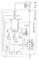
- FIG. 1 illustrates a conventional charging circuit.
- FIG. 2 and FIG. 3 illustrate the operation of a PWM comparator in FIG. 1 .
- FIG. 4 illustrates temperature characteristics of a thermistor in FIG. 1 .
- FIG. 5 illustrates temperature characteristics of a voltage supplied to a window comparator in FIG. 1 .
- a conventional charging circuit CHG uses a DC-DC converter of a PWM control method and has a main switching transistor T 1 , a synchronous rectification transistor T 2 , a choke coil L 1 , a smoothing capacitor C 1 , a current measurement resistor RS, and a control circuit CTL.
- the main switching transistor T 1 is formed by an n-type transistor. An input pin of the main switching transistor T 1 is coupled to a pin P 1 for receiving an input voltage Vi. An output pin of the main switching transistor T 1 is coupled to one end of the choke coil L 1 . A control pin of the main switching transistor T 1 receives an output signal Q 1 of a PWM comparator PCMP in the control circuit CTL.
- the synchronous rectification transistor T 2 is formed by an n-type transistor. An input pin of the synchronous rectification transistor T 2 is coupled to a ground line. An output pin of the synchronous rectification transistor T 2 is coupled to the one end of the choke coil L 1 .
- a control pin of the synchronous rectification transistor T 2 receives an output signal /Q 1 a of a gate circuit G 2 in the control circuit CLT.
- the other end of the choke coil L 1 is coupled to one end of the smoothing capacitor C 1 and one end of the current measurement resistor RS.
- the other end of the current measurement resistor RS is coupled to a ground line.
- the other end of the current measurement resistor RS is coupled to a pin P 2 for supplying an output voltage Vo to a secondary battery BTR.
- the control circuit CTL includes a voltage amplifier AMP, voltage generators E 1 , E 2 , error amplifiers ERA 1 , ERA 2 , resistors R 1 to R 3 , an n-type transistor T 3 , a triangular wave oscillator OSC, the PWM comparator PCMP, gate circuits G 1 , G 2 , and a window comparator WCMP.
- the voltage amplifier AMP receives, at a non-inverting input pin, a voltage of the one end of the current measurement resistor RS, and receives, at an inverting input pin, a voltage of the other end of the current measurement resistor RS (output voltage Vo).
- the voltage amplifier AMP amplifies a voltage difference between the voltage of the one end of the current measurement resistor RS and the voltage of the other end of the current measurement resistor RS to generate a voltage Vc. Therefore, the voltage Vc generated by the voltage amplifier AMP corresponds to an output current of the charging circuit CHG (charging current of the secondary battery BTR).
- the voltage generator El generates a reference voltage Ve 1 .
- the error amplifier ERA 1 receives the reference voltage Ve 1 at a non-inverting input pin and receives the voltage Vc at an inverting input pin. Consequently, the error amplifier ERA 1 amplifiers a voltage difference between the reference voltage Ve 1 and the voltage Vc to generate an output signal DF 1 .
- the voltage generator E 2 generates a reference voltage Ve 2 .
- the resistors R 1 , R 2 and the transistor T 3 are coupled in series between the pin P 2 and the ground line.
- a control pin of the transistor T 3 receives a stop signal /STP supplied from the gate circuit G 1 .
- the error amplifier ERA 2 receives the reference voltage Ve 2 at a non-inverting input pin and receives, at an inverting input pin, a voltage of a coupling node of the resistors R 1 , R 2 (a voltage resulting from the division of the output voltage Vo by the resistors R 1 , R 2 and the transistor T 3 ). Consequently, the error amplifier ERA 2 amplifies a voltage difference between the reference voltage Ve 2 and the voltage of the coupling node of the resistors R 1 , R 2 to generate an output signal DF 2 .
- the triangular wave oscillator OSC generates a triangular wave signal TW with a predetermined period.
- the PWM comparator PCMP is a voltage to pulse width converter which compares a lower one of a voltage of a first non-inverting input pin and a voltage of a second non-inverting input pin with a voltage of an inverting input pin, and sets the output signal Q 1 (/Q 1 ) high (low) when the voltage of the inverting input pin is lower, while setting the output signal Q 1 (/Q 1 ) low (high) when the voltage of the inverting input pin is higher.
- the PWM comparator PCMP receives the output signal DF 1 of the error amplifier ERA 1 at the first non-inverting input pin, receives the output signal DF 2 of the error amplifier ERA 2 at the second non-inverting pin, and receives the triangular wave signal TW at the inverting input pin.
- the PWM comparator PCMP compares the voltage of the output signal DF 1 of the error amplifier ERA 1 and the voltage of the triangular wave signal TW, and sets the output signal Q 1 high when the voltage of the output signal DF 1 of the error amplifier ERA 1 is higher than the voltage of the triangular wave signal TW, while setting the output signal Q 1 low when the voltage of the output signal DF 1 of the error amplifier ERA 1 is lower than the voltage of the triangular wave signal TW.
- the PWM comparator PCMP compares the voltage of the output signal DF 2 of the error amplifier ERA 2 and the voltage of the triangular wave signal TW, and sets the output signal Q 1 high when the voltage of the output signal DF 2 of the error amplifier ERA 2 is higher than the voltage of the triangular wave signal TW, while setting the output signal Q 1 low when the voltage of the output signal DF 2 of the error amplifier ERA 2 is lower than the voltage of the triangular wave signal TW.
- the resistor R 3 is coupled between a supply line of a pull-up voltage Vh and a pin P 3 .
- the pin P 3 is coupled to one end of a temperature measurement thermistor Th in the secondary battery BTR.
- the other end of the thermistor Th is coupled to a ground line.
- the thermistor Th is a temperature-sensitive resistor element whose resistance value changes according to temperature, and has temperature characteristics as illustrated in FIG. 4 . Since the constant voltage Vh is applied to a serial resistor formed by the resistor R 3 and the thermistor Th, a voltage Vt 1 of the pin P 3 supplied to the window comparator WCMP has temperature characteristics as illustrated in FIG. 5 .
- the window comparator WCMP sets a stop signal STP 1 low when the voltage Vt 1 is higher than ⁇ V and lower than ⁇ V, while setting the stop signal STP 1 high when the voltage Vt 1 is lower than ⁇ V or the voltage Vt 1 is higher than ⁇ V, where ⁇ V is a value that the voltage Vt 1 has when the temperature of the secondary battery BTR is the highest temperature in the tolerable range and ⁇ V is a value that the voltage Vt 1 has when the temperature of the secondary battery BTR is the lowest temperature in the tolerable range.
- the gate circuit G 1 sets the stop signal /STP low when at least one of stop signals STP 1 , STP 2 is set high, while setting the stop signal /STP high when the stop signals STP 1 , STP 2 are both set low.
- the stop signal STP 2 is a signal for requesting activation/stop of the charging circuit CHG, and is set high when the stop of the charging circuit CHG is requested, while being set low when the activation of the charge circuit CHG is requested.
- the gate circuit G 2 supplies the control pin of the synchronous rectification transistor T 2 with the output signal /Q 1 of the PWM comparator PCMP as the output signal /Q 1 a , and when the stop signal /STP is set low, the gate circuit G 2 supplies the control pin of the synchronous rectification transistor T 2 with the low level signal as the output signal /Q 1 a.
- the synchronous rectification transistor T 2 turns off, so that a current is supplied from an input side to a load via the choke coil L 1 . Since a voltage difference between the input voltage Vi and the output voltage Vo is applied to the both ends of the choke coil L 1 , a current flowing through the choke coil L 1 increases with time, and the current supplied to the load also increases with time. Further, energy is accumulated in the choke coil L 1 when the current flows through the choke coil L 1 .
- an average input current Ii is expressed by an equation (2) using the ON period Ton of the main switching transistor T 1 , the OFF period Toff of the main switching transistor T 1 , and an output current Io.
- Ii ⁇ T on/( T on+ T off) ⁇ Io (2)
- the output voltage Vo varies due to the variation of the input voltage Vi, it is possible to keep the output voltage Vo constant by controlling a ratio of the ON period/OFF period of the main switching transistor T 1 based on the detected variation of the output voltage Vo.
- the output voltage Vo varies due to the variation of the load, it is also possible to keep the output voltage Vo constant by controlling the ratio of the ON period/OFF period of the main switching transistor T 1 based on the detected variation of the output voltage Vo.
- the charging circuit CHG in accordance with an increase in a load current, a current flowing through the current measurement resistor RS increases, and a voltage decrease occurring at the both ends of the current measurement resistor RS becomes great.
- the great voltage decrease occurring at the both ends of the current measurement resistor RS results in a small voltage difference between the voltage of the non-inverting input pin and the voltage of the inverting input pin in the error amplifier ERA 1 , so that the voltage of the output signal DF 1 of the error amplifier ERA 1 lowers.
- a pulse width (high-level period) of the output signal Q 1 of the PWM comparator PCMP reduces, the output voltage Vo lowers, resulting in a decreased charging current of the secondary battery BTR.
- controlling the output voltage Vo by controlling the ratio of the ON period/OFF period of the main switching transistor T 1 makes it possible to control a charging current and a charging voltage of the secondary battery BTR.
- the stop signal STP 1 supplied from the window comparator WCMP is set high since the voltage Vt 1 becomes lower than ⁇ V. Consequently, the stop signal /STP supplied from the gate circuit G 1 is set low, so that the charging circuit CHG stops and the charging of the secondary battery BTR is stopped.
- the stop signal STP 1 is set high since the voltage Vt 1 becomes higher than ⁇ V. Consequently, the stop signal /STP is set low, so that the charging circuit CHG stops and the charging of the secondary battery BTR is stopped.
- the stop signal /STP supplied from the gate circuit G 1 is set low, and consequently, the output signal /Q 1 a of the gate circuit G 2 is set low to turn off the synchronous rectification transistor T 2 , which prevents the secondary battery BTR from being discharged via the synchronous rectification transistor T 2 .
- the stop signal /STP is set low, and consequently, the transistor T 3 turns off, which prevents the secondary battery BTR from being discharged via the resistors R 1 , R 2 and the transistor T 3 .
- related arts include Japanese Unexamined Patent Application Publication No. H08-33230, Japanese Unexamined Patent Application Publication No. H05-207671, Japanese Unexamined Patent Application Publication No. H05-227677, Japanese Unexamined Patent Application Publication No. H06-165408, Japanese Unexamined Patent Application Publication No. H10-32475, Japanese Unexamined Patent Application Publication No. H11-150885, Japanese Unexamined Patent Application Publication No. 2001-211562, Japanese Unexamined Patent Application Publication No. H06-284593, Japanese Unexamined Patent Application Publication No. 2005-274372, and so on.
- the conventional charging circuit is structured to stop charging the secondary battery when the temperature of the secondary battery is beyond the tolerable range. This causes the following situations. That is, immediately after the secondary battery is discharged, the temperature of the secondary battery is relatively high. If the charging of the secondary battery is started in this state, the charging of the secondary battery is stopped immediately due to the high temperature, and the charging of the secondary battery is kept stopped until the temperature of the secondary battery lowers to a temperature within the tolerable range. Further, immediately after the portable electronics device is driven by using the power supply from the secondary battery, the temperature of the secondary battery is relatively high.
- the temperature of the secondary battery quickly increases up to a temperature beyond the tolerable range, and in some cases, the start and stop of the charging of the secondary battery are frequently repeated until the temperature of the portable electronics device sufficiently decreases.
- a power supply circuit (a power supply control circuit applied in the power supply circuit) charging a secondary battery by a DC-DC converter using a switching element and an inductance element includes a current adjustment circuit.
- the current adjustment circuit adjusts a charging current of the secondary battery by turning on/off the switching element according to a voltage difference of a lower one of a reference voltage and a first control voltage corresponding to a temperature of the secondary battery from a current detection voltage corresponding to the charging current of the secondary battery (current adjustment operation).
- FIG. 1 is an explanatory diagram illustrating a conventional charging circuit
- FIG. 2 is an explanatory chart (No. 1 ) illustrating the operation of a PWM comparator in FIG. 1 ;
- FIG. 3 is an explanatory chart (No. 2 ) illustrating the operation of the PWM comparator in FIG. 1 ;
- FIG. 4 is an explanatory chart illustrating temperature characteristics of a thermistor in FIG. 1 ;
- FIG. 5 is an explanatory chart illustrating temperature characteristic of a voltage supplied to a window comparator in FIG. 1 ;
- FIG. 6 is an explanatory diagram illustrating a first embodiment
- FIG. 7 is an explanatory diagram illustrating a second embodiment
- FIG. 8 is an explanatory chart illustrating output characteristics of a charging circuit of the second embodiment
- FIG. 9 is an explanatory diagram illustrating a third embodiment
- FIG. 10 is an explanatory diagram illustrating a fourth embodiment.
- FIG. 11 is an explanatory diagram illustrating a fifth embodiment.
- the charging current of the secondary battery can be decreased as the temperature of the secondary battery increases. Since a temperature increase rate of the secondary battery greatly depends on the charging current, it is possible to suppress the temperature increase accompanying the charging of the secondary battery, which makes it possible to charge the secondary battery in a relatively high temperature state.
- the current adjustment circuit uses, in addition to the reference voltage and the first control voltage, a second control voltage corresponding to a temperature of the power supply circuit and a third control voltage which is set to one of a voltage higher than the reference voltage and a voltage lower than the reference voltage according to a charging voltage of the secondary battery, and turns on/off the switching element according to a voltage difference of a lowest one of the reference voltage and the first to third control voltages from the current detection voltage.
- the power supply circuit itself also generates heat while charging the secondary battery, and since the power supply circuit is generally disposed near the secondary battery, the temperature of the secondary battery increases due to the influence of heat caused by the heat generation of the power supply circuit. Therefore, by additionally using the second control voltage, the current adjustment circuit can adjust the charging current of the secondary battery with high precision. Further, the additional use of the third control voltage by the current adjustment circuit enables the power supply circuit to have output characteristics such that the charging current of the secondary battery is set small when the charging voltage of the secondary battery is lower than a predetermined voltage and the charging current of the secondary battery is set large when the charging voltage of the secondary battery is higher than the predetermined voltage.
- the power supply circuit further includes a non-linear conversion circuit.
- the non-linear conversion circuit non-linearly converts the first control voltage according to a predetermined conversion rule to generate a first converted control voltage (non-linear conversion operation).
- the current adjustment circuit uses the first converted control voltage instead of the first control voltage.
- the voltage generated by the non-linear conversion circuit is set lower than the reference voltage.
- the current adjustment circuit excludes the reference voltage from voltages to be used. This can simplify the current adjustment circuit, realizing a reduced circuit scale of the power supply circuit.
- the non-linear conversion circuit generates a second and a third converted control voltage by non-linearly converting a second control voltage corresponding to a temperature of the power supply circuit and a charging voltage of the secondary battery according to a predetermined conversion rule.
- the current adjustment circuit uses the second and third converted control voltages in addition to the first converted control voltage, and turns on/off the switching element according to a voltage difference of a lowest one of the first to third converted control voltages from the current detection voltage.
- the current adjustment circuit can adjust the charging current of the secondary battery with high precision.
- the additional use of the third converted control voltage by the current adjustment circuit enables the power supply circuit to have output characteristics such that that the charging current of the secondary battery is set small when the charging voltage of the secondary battery is lower than a predetermined voltage and the charging current of the secondary battery is set large when the charging voltage of the secondary battery is higher than the predetermined voltage.
- the non-linear conversion circuit includes a conversion rule changing circuit.
- the conversion rule changing circuit changes the conversion rule according to the secondary battery (conversion rule changing operation).
- the conversion rule changing circuit changes the conversion rule by using a communication circuit communicating with an external device. Providing the conversion rule changing circuit makes it possible to adjust the charging current of the secondary battery according to the secondary battery with high precision.
- FIG. 6 illustrates a first embodiment.
- the first embodiment will be described, and the same reference numerals and symbols as those used in FIG. 1 are used to designate the same elements as the elements described in FIG. 1 , and detailed description thereof will be omitted.
- a charging circuit CHGa of the first embodiment is structured such that in the charging circuit CHG in FIG. 1 , the control circuit CTL is replaced by a control circuit CTLa.
- the charging circuit CHGa is embodied by a semiconductor device and is mounted on a portable electronics device to be used for charging a secondary battery BTR.
- the control circuit CTLa is structured such that in the control circuit CTL, the gate circuit G 1 is removed and the window comparator WCMP and the error amplifier ERA 1 are replaced by a window comparator WCMPa and an error amplifier ERA 1 a.
- the window comparator WCMPa sets a stop signal /STP high when a voltage Vt 1 is higher than ⁇ V and lower than ⁇ V, while setting the stop signal /STP low when the voltage Vt 1 is lower than ⁇ V or when the voltage Vt 1 is higher than ⁇ V.
- the error amplifier ERA 1 a receives a reference voltage Ve 1 at a first non-inverting input pin, receives the voltage Vt 1 at a second non-inverting input pin, and receives a voltage Vc at an inverting input pin.
- the error amplifier ERA 1 a amplifies a voltage difference of a lower one of the voltage of the first non-inverting input pin and the voltage of the second non-inverting input pin from the voltage of the inverting input pin to generate an output signal DF 1 . Therefore, the error amplifier ERA 1 a amplifies a voltage difference between the reference voltage Ve 1 and the voltage Vc to generate the output signal DF 1 when the voltage Vt 1 is higher than the reference voltage Ve 1 , and amplifies a voltage difference between the voltage Vt 1 and the voltage Vc to generate the output signal DF 1 when the voltage Vt 1 is lower than the reference voltage Ve 1 .
- the voltage Vt 1 of a pin P 3 supplied to the window comparator WCMPa has temperature characteristics that its voltage value decreases as a temperature of the secondary battery BTR increases as illustrated in FIG. 5 .
- the temperature of the secondary battery BTR increases when it is charged and discharged, but since a temperature increase rate greatly depends on a charging current and a discharging current, the temperature increase rate lowers as the charging current and the discharging current decrease.
- the charging current of the secondary battery BTR is adjusted based on the reference voltage Ve 1 when the temperature of the secondary battery BTR is low, but the charging current of the secondary battery BTR is adjusted based on the voltage Vt 1 when the temperature of the secondary battery BTR increases.
- the charging current of the secondary battery BTR can be decreased as the temperature of the secondary battery BTR is higher. Therefore, it is possible to prevent the secondary battery BTR from having a temperature beyond a tolerable range, which makes it possible to charge the secondary battery BTR in a relatively high-temperature state.
- FIG. 7 illustrates a second embodiment.
- FIG. 8 illustrates output characteristics of a charging circuit of the second embodiment.
- a charging circuit CHGb of the second embodiment is structured such that in the charging circuit CHGa of the first embodiment, the control circuit CTLa is replaced by a control circuit CTLb.
- the charging circuit CHGb is embodied by a semiconductor device and is mounted on a portable electronics device to be used for charging a secondary battery BTR.
- the control circuit CTLb is structured such that in the control circuit CTLa, voltage generators E 3 to E 5 , a voltage comparator VCMP, and a switch circuit SW are added, and the error amplifier ERA 1 a is replaced by an error amplifier ERA 1 b.
- the voltage generator E 3 generates a reference voltage Ve 3 .
- the voltage comparator VCMP receives an output voltage Vo (a charging voltage of the secondary battery BTR) at a non-inverting input pin and receives the reference voltage Ve 3 at an inverting input pin. With this structure, the voltage comparator VCMP sets an output signal high when the charging voltage of the secondary battery BTR is higher than the reference voltage Ve 3 , while setting the output signal low when the charging voltage of the secondary battery BTR is lower than the reference voltage Ve 3 .
- the voltage generator E 4 generates a reference voltage Ve 4 higher than the reference voltage Ve 1 .
- the voltage generator E 5 generates a reference voltage Ve 5 lower than the reference voltage Ve 1 .
- the switch circuit SW outputs the reference voltage Ve 4 as a voltage Vs when the output signal of the voltage comparator VCMP is set high (when the charging voltage of the secondary battery BTR is higher than the reference voltage Ve 3 ).
- the switch circuit SW outputs the reference voltage Ve 5 as the voltage Vs when the output signal of the voltage comparator VCMP is set low (when the charging voltage of the secondary battery BTR is lower than the reference voltage Ve 3 ).
- the error amplifier ERA 1 b receives the reference voltage Ve 1 at a first non-inverting input pin, receives a voltage Vt 1 at a second non-inverting input pin, receives a voltage Vt 2 at a third non-inverting input pin, receives the voltage Vs at a fourth non-inverting input pin, and receives a voltage Vc at an inverting input pin.
- the error amplifier ERA 1 b amplifies a voltage difference of the lowest one of the voltages of the first to fourth non-inverting input pins from the voltage of the inverting input pin to generate an output signal DF 1 .
- the error amplifier ERA 1 b amplifies a voltage difference of the lowest one of the reference voltage Ve 1 , the voltage Vt 1 , the voltage Vt 2 , and the voltage Vs from the voltage Vc to generate the output signal DF 1 .
- the voltage Vt 2 corresponds to a temperature of the charging circuit CHGb.
- a correlation between the voltage Vt 2 and the temperature of the charging circuit CHGb is the same as a correlation between the voltage Vt 1 and the temperature of the secondary battery BTR.
- the second embodiment as described above can provide the same effects as those of the first embodiment.
- a charging current of the secondary battery BTR is adjusted based on the voltage Vt 2 corresponding to the temperature of the charging circuit CHGb. This enables precise adjustment of the charging current of the secondary battery BTR.
- the charging current of the secondary battery BTR is adjusted based on the reference voltage Ve 1 if the charging voltage of the secondary battery BTR is higher than the reference voltage Ve 3 , and the charging current of the secondary battery BTR is adjusted based on the reference voltage Ve 5 lower than the reference voltage Ve 1 if the charging voltage of the secondary battery BTR is lower than the reference voltage Ve 3 .
- the charging current of the secondary battery BTR (the output current of the charging circuit CHGb) becomes a current 10 when the charging voltage of the secondary battery BTR (the output voltage Vo of the charging circuit CHGb) is lower than a voltage V 0
- the charging current of the secondary battery BTR becomes a current 11 when the charging voltage of the secondary battery BTR is higher than the voltage V 0 , as illustrated in FIG. 8 .
- FIG. 9 illustrates a third embodiment.
- the third embodiment will be described, and the same reference numerals and symbols as those used in the first embodiment are used to designate the same elements as the elements described in the first embodiment, and detailed description thereof will be omitted.
- a charging circuit CHGc of the third embodiment is structured such that in the charging circuit CHGa of the first embodiment, the control circuit CTLa is replaced by a control circuit CTLc.
- the charging circuit CHGc is embodied by a semiconductor device and is mounted on a portable electronics device to be used for charging a secondary battery BTR.
- the control circuit CTLc is structured such that in the control circuit CTLa, a non-linear conversion circuit NLC is added.
- the non-linear conversion circuit NLC includes an A/D converter ADC, a non-volatile memory MEM, a D/A converter DAC, and a communication circuit COM.
- the A/D converter ADC converts a voltage Vt 1 to a digital value to supply the digital value to the non-volatile memory MEM.
- the non-volatile memory MEM receives, as an address, the digital value supplied from the A/D converter ADC, and reads the digital value stored in the address to supply the read digital value to the D/A converter DAC.
- the D/A converter DAC converts the digital value supplied from the non-volatile memory MEM to an analog voltage to supply the analog voltage as a voltage Vt 1 a to a second non-inverting input pin of an error amplifier ERA 1 a .
- the communication circuit COM which is formed by using a serial interface circuit or the like (for example, IIC), is capable of communicating with an external device via a pin P 4 and rewrites the digital value stored in the non-volatile memory MEM according to a request from the external device.
- a charging current of the secondary battery BTR is adjusted based on a reference voltage Ve 1 when the voltage Vt 1 a supplied from the D/A converter DAC is higher than the reference voltage Ve 1 , and the charging current of the secondary battery BTR is adjusted based on the voltage Vt 1 a when the voltage Vt 1 a is lower than the reference voltage Ve 1 .
- the digital value stored in the non-volatile memory MEM is rewritable from the external device via the communication circuit COM, which makes it possible to adjust the charging current of the secondary battery BTR according to characteristics of the secondary battery BTR. Therefore, as compared to the first embodiment where the charging current of the secondary battery BTR is settable only to a current value which depends on the temperature characteristics of the thermistor Th, it is possible to more greatly improve convenience.
- FIG. 10 illustrates a fourth embodiment.
- the fourth embodiment will be described, and the same reference numerals and symbols as those used in the first and third embodiments are used to designate the same elements as the elements described in the first and third embodiments, and detailed description thereof will be omitted.
- a charging circuit CHGd of the fourth embodiment is structured such that in the charging circuit CHGc of the third embodiment, the control circuit CTLc is replaced by a control circuit CTLd.
- the charging circuit CHGd is embodied by a semiconductor device and is mounted on a portable electronics device to be used for charging a secondary battery BTR.
- the control circuit CTLd is structured such that in the control circuit CTLc, the voltage generator E 1 is removed and the error amplifier ERA 1 a is replaced by an error amplifier ERA 1 c.
- the error amplifier ERA 1 c receives a voltage Vt 1 a at a non-inverting input pin and receives a voltage Vc at an inverting input pin. With this structure, the error amplifier ERA 1 c amplifies a voltage difference between the voltage Vt 1 a and the voltage Vc to generate an output signal DF 1 .
- a digital value stored in a non-volatile memory MEM is set so that the voltage Vt 1 a supplied from a D/A converter DAC becomes lower than the reference voltage Ve 1 .
- the fourth embodiment as described above can also provide the same effects as those of the first and third embodiments, and in addition, can reduce circuit scale since the voltage generator E 1 is removed and the error amplifier ERA 1 c having a less number of the non-inverting input pins than the error amplifier ERA 1 a is used.
- FIG. 11 illustrates a fifth embodiment.
- the fifth embodiment will be described, and the same reference numerals and symbols as those used in the first to fourth embodiments are used to designate the same elements as the elements described in the first to fourth embodiments, and detailed description thereof will be omitted.
- a charging circuit CHGe of the fifth embodiment is structured such that in the charging circuit CHGc of the third embodiment, the control circuit CTLc is replaced by a control circuit CTLe.
- the charging circuit CHGe is embodied by a semiconductor device and is mounted on a portable electronics device to be used for charging a secondary battery BTR.
- the control circuit CTLe is structured such that in the control circuit CTLc, the non-linear conversion circuit NLC and the error amplifier ERA 1 a are replaced by a non-linear conversion circuit NLCa and an error amplifier ERA 1 d.
- the non-linear conversion circuit NLCa includes an A/D converter ADCa, a non-volatile memory MEMa, a D/A converter DACa, and a communication circuit COMa.
- the A/D converter ADCa has a first to a third channel.
- the first channel of the A/D converter ADCa converts a voltage Vt 1 to a digital value to supply the digital value to the non-volatile memory MEMa.
- the second channel of the A/D converter ADCa converts a voltage Vt 2 to a digital value to supply the digital value to the non-volatile memory MEMa.
- the third channel of the A/D converter ADCa converts an output voltage Vo (a charging voltage of the secondary battery BTR) to a digital value to supply the digital value to the non-volatile memory MEMa.
- the non-volatile memory MEMa has a first to a third memory section.
- the first memory section of the non-volatile memory MEMa receives, as an address, the digital value supplied from the first channel of the A/D converter ADCa, and reads the digital value stored in the address to supply the read digital value to the D/A converter DACa.
- the second memory section of the non-volatile memory MEMa receives, as an address, the digital value supplied from the second channel of the A/D converter ADCa and reads the digital value stored in the address to supply the read digital value to the D/A converter DACa.
- the third memory section of the non-volatile memory MEMa receives, as an address, the digital value supplied from the third channel of the A/D converter ADCa and reads the digital value stored in the address to supply the read digital value to the D/A converter DACa.
- the D/A converter DACa has a first to a third channel.
- the first channel of the D/A converter DACa converts the digital value supplied from the first memory section of the non-volatile memory MEMa to an analog voltage to output the analog voltage as a voltage Vt 1 a .
- the second channel of the D/A converter DACa converts the digital value supplied from the second memory section of the non-volatile memory MEMa to an analog voltage to output the analog voltage as a voltage Vt 2 a .
- the third channel of the D/A converter DACa converts the digital value supplied from the third memory section of the non-volatile memory MEMa to an analog voltage to output the analog voltage as a voltage Vs.
- the communication circuit COMa which is formed by using a serial interface or the like (for example, IIC), is capable of communicating with an external device via a pin P 4 and rewrites the digital values stored in the first to third memory sections of the non-volatile memory MEMa according to a request from the external device.
- the digital values stored in the first to third memory sections of the non-volatile memory MEMa are set so that the voltages Vt 1 a , Vt 2 a , Vs supplied from the D/A converter DACa become lower than the reference voltage Ve 1 .
- the error amplifier ERA 1 d receives the voltage Vt 1 a at a first non-inverting input pin, receives the voltage Vt 2 a at a second non-inverting input pin, receives the voltage Vs at a third non-inverting input pin, and receives the voltage Vc at an inverting input pin.
- the error amplifier ERA 1 d amplifies a voltage difference of the lowest one of the voltages of the first to third non-inverting input pins from the voltage of the inverting input pin to generate an output signal DF 1 .
- the error amplifier ERA 1 d amplifies a voltage difference of the lowest one of the voltage Vt 1 a , the voltage Vt 2 a , and the voltage Vs from the voltage Vc to generate the output signal DF 1 .
- the fifth embodiment as described above can also provide the same effects as those of the first to fourth embodiments.
- the first to fifth embodiments describe the examples where the charging circuit is embodied by the semiconductor device, but for example, the charging circuit may be embodied by a module (a printed-circuit board or the like). Further, the first to fifth embodiments describe the examples where the present embodiment is applied to the case in which the charging circuit and the secondary battery are separately mounted on the portable electronics device, but for example, the present embodiment may be applied to a case in which a secondary battery pack including the charging circuit and the secondary battery is mounted on the portable electronics device.
Abstract
Description
Vo={Ton/(Ton+Toff)}×Vi (1)
Ii={Ton/(Ton+Toff)}×Io (2)
Claims (20)
Applications Claiming Priority (2)
| Application Number | Priority Date | Filing Date | Title |
|---|---|---|---|
| JP2007035987A JP4642792B2 (en) | 2007-02-16 | 2007-02-16 | Power supply circuit, power supply control circuit, and power supply control method |
| JP2007-035987 | 2007-02-16 |
Publications (2)
| Publication Number | Publication Date |
|---|---|
| US20080197814A1 US20080197814A1 (en) | 2008-08-21 |
| US7960946B2 true US7960946B2 (en) | 2011-06-14 |
Family
ID=39706088
Family Applications (1)
| Application Number | Title | Priority Date | Filing Date |
|---|---|---|---|
| US12/032,237 Active 2028-05-12 US7960946B2 (en) | 2007-02-16 | 2008-02-15 | Power supply circuit, power supply control circuit, and power supply control method |
Country Status (5)
| Country | Link |
|---|---|
| US (1) | US7960946B2 (en) |
| JP (1) | JP4642792B2 (en) |
| KR (1) | KR101073595B1 (en) |
| CN (1) | CN101247051B (en) |
| TW (1) | TWI368378B (en) |
Cited By (2)
| Publication number | Priority date | Publication date | Assignee | Title |
|---|---|---|---|---|
| DE102013205290A1 (en) | 2012-04-03 | 2013-10-10 | GM Global Technology Operations LLC (n.d. Ges. d. Staates Delaware) | Rubber crack reducing agent in polyelectrolyte membranes |
| US9065292B2 (en) | 2010-08-23 | 2015-06-23 | California Institute Of Technology | Methods and systems for charging electrochemical cells |
Families Citing this family (7)
| Publication number | Priority date | Publication date | Assignee | Title |
|---|---|---|---|---|
| TWI403062B (en) * | 2009-02-05 | 2013-07-21 | Via Tech Inc | Automatic charger protection circuit of a charger of a electronic device and method |
| FI123893B (en) * | 2009-11-27 | 2013-12-13 | Teknoware Oy | Arrangement for recharging batteries |
| KR101102413B1 (en) * | 2010-05-17 | 2012-01-05 | 제주산업정보대학 산학협력단 | System for monitoring remote automatic voltage regulator using blockout compensator and method therefor |
| WO2013128808A1 (en) * | 2012-02-29 | 2013-09-06 | Necエナジーデバイス株式会社 | Battery control system, battery pack, electronic device, and charger |
| CN103701183B (en) * | 2013-12-31 | 2015-09-30 | 杭州士兰微电子股份有限公司 | Multi-branch circuit feedback charger circuit and charging method |
| KR20210007456A (en) * | 2019-07-11 | 2021-01-20 | 삼성전자주식회사 | Method and circuit for monitoring secondary power source, and storage device comprising the same |
| TWI717838B (en) * | 2019-09-18 | 2021-02-01 | 宏碁股份有限公司 | Power supply device |
Citations (15)
| Publication number | Priority date | Publication date | Assignee | Title |
|---|---|---|---|---|
| JPH05207671A (en) | 1992-01-23 | 1993-08-13 | Sanyo Electric Co Ltd | Charger |
| JPH05227677A (en) | 1990-10-12 | 1993-09-03 | Compaq Computer Corp | Circuit and system for charging battery |
| JPH06165408A (en) | 1992-11-20 | 1994-06-10 | Fuji Electric Co Ltd | Charging device of nickel-cadmium battery |
| JPH06284593A (en) | 1993-03-19 | 1994-10-07 | Canon Business Mach Inc | Method and circuit for charging secondary battery |
| JPH0833230A (en) | 1994-07-08 | 1996-02-02 | Toshiba Corp | Uninterruptible power supply |
| US5703468A (en) * | 1995-03-17 | 1997-12-30 | Petrillo; Gino A. | Electrical charge control apparatus and method for photovoltaic energy conversion systems |
| JPH1032475A (en) | 1996-05-17 | 1998-02-03 | Denso Corp | Load driving circuit |
| US5731686A (en) * | 1993-07-30 | 1998-03-24 | Texas Instruments Incorporated | Embedded battery overtemperature protection and voltage regulator circuitry |
| JPH11150885A (en) | 1997-11-17 | 1999-06-02 | Ricoh Co Ltd | Method for charging secondary battery |
| US6133712A (en) | 1998-08-21 | 2000-10-17 | Fairchild Korea Semiconductor Ltd. | Battery charge controller having an adjustable termination current |
| JP2001211562A (en) | 1999-12-08 | 2001-08-03 | Tai-Her Yang | Charging circuit having plurality of modes |
| JP2005274372A (en) | 2004-03-25 | 2005-10-06 | Chofu Seisakusho Co Ltd | Temperature detector |
| US20050275379A1 (en) * | 2004-06-14 | 2005-12-15 | Fujitsu Limited | Charge control that keeps constant input voltage supplied to battery pack |
| US20080094865A1 (en) * | 2006-10-21 | 2008-04-24 | Advanced Analogic Technologies, Inc. | Supply Power Control with Soft Start |
| US7598710B2 (en) * | 2006-12-08 | 2009-10-06 | Monolithic Power Systems, Inc. | Battery charger with temperature control |
Family Cites Families (5)
| Publication number | Priority date | Publication date | Assignee | Title |
|---|---|---|---|---|
| CN2150659Y (en) * | 1993-03-29 | 1993-12-22 | 潘峰 | Quick-acting charger for battery |
| KR100263551B1 (en) * | 1996-10-12 | 2000-08-01 | 윤종용 | Secondary battery charging circuit |
| JP2000184612A (en) * | 1998-10-08 | 2000-06-30 | Fujitsu Ltd | Dc-dc converter, its control method and its control circuit |
| JP2004304957A (en) * | 2003-03-31 | 2004-10-28 | Sony Corp | Charging system |
| JP5029862B2 (en) * | 2006-03-31 | 2012-09-19 | 日立工機株式会社 | Charger |
-
2007
- 2007-02-16 JP JP2007035987A patent/JP4642792B2/en active Active
-
2008
- 2008-01-28 KR KR1020080008551A patent/KR101073595B1/en active IP Right Grant
- 2008-02-13 CN CN2008100059052A patent/CN101247051B/en active Active
- 2008-02-15 TW TW097105315A patent/TWI368378B/en not_active IP Right Cessation
- 2008-02-15 US US12/032,237 patent/US7960946B2/en active Active
Patent Citations (16)
| Publication number | Priority date | Publication date | Assignee | Title |
|---|---|---|---|---|
| JPH05227677A (en) | 1990-10-12 | 1993-09-03 | Compaq Computer Corp | Circuit and system for charging battery |
| JPH05207671A (en) | 1992-01-23 | 1993-08-13 | Sanyo Electric Co Ltd | Charger |
| JPH06165408A (en) | 1992-11-20 | 1994-06-10 | Fuji Electric Co Ltd | Charging device of nickel-cadmium battery |
| JPH06284593A (en) | 1993-03-19 | 1994-10-07 | Canon Business Mach Inc | Method and circuit for charging secondary battery |
| US5731686A (en) * | 1993-07-30 | 1998-03-24 | Texas Instruments Incorporated | Embedded battery overtemperature protection and voltage regulator circuitry |
| JPH0833230A (en) | 1994-07-08 | 1996-02-02 | Toshiba Corp | Uninterruptible power supply |
| US5703468A (en) * | 1995-03-17 | 1997-12-30 | Petrillo; Gino A. | Electrical charge control apparatus and method for photovoltaic energy conversion systems |
| JPH1032475A (en) | 1996-05-17 | 1998-02-03 | Denso Corp | Load driving circuit |
| JPH11150885A (en) | 1997-11-17 | 1999-06-02 | Ricoh Co Ltd | Method for charging secondary battery |
| US6133712A (en) | 1998-08-21 | 2000-10-17 | Fairchild Korea Semiconductor Ltd. | Battery charge controller having an adjustable termination current |
| KR100271094B1 (en) | 1998-08-21 | 2000-11-01 | 김덕중 | Charge contoller |
| JP2001211562A (en) | 1999-12-08 | 2001-08-03 | Tai-Her Yang | Charging circuit having plurality of modes |
| JP2005274372A (en) | 2004-03-25 | 2005-10-06 | Chofu Seisakusho Co Ltd | Temperature detector |
| US20050275379A1 (en) * | 2004-06-14 | 2005-12-15 | Fujitsu Limited | Charge control that keeps constant input voltage supplied to battery pack |
| US20080094865A1 (en) * | 2006-10-21 | 2008-04-24 | Advanced Analogic Technologies, Inc. | Supply Power Control with Soft Start |
| US7598710B2 (en) * | 2006-12-08 | 2009-10-06 | Monolithic Power Systems, Inc. | Battery charger with temperature control |
Cited By (3)
| Publication number | Priority date | Publication date | Assignee | Title |
|---|---|---|---|---|
| US9065292B2 (en) | 2010-08-23 | 2015-06-23 | California Institute Of Technology | Methods and systems for charging electrochemical cells |
| DE102013205290A1 (en) | 2012-04-03 | 2013-10-10 | GM Global Technology Operations LLC (n.d. Ges. d. Staates Delaware) | Rubber crack reducing agent in polyelectrolyte membranes |
| DE102013205290B4 (en) | 2012-04-03 | 2021-11-18 | GM Global Technology Operations, LLC (n.d. Ges. d. Staates Delaware) | Rubber crack reducing agent in polyelectrolyte membranes |
Also Published As
| Publication number | Publication date |
|---|---|
| KR20080076733A (en) | 2008-08-20 |
| CN101247051A (en) | 2008-08-20 |
| TWI368378B (en) | 2012-07-11 |
| CN101247051B (en) | 2012-08-22 |
| JP4642792B2 (en) | 2011-03-02 |
| TW200841551A (en) | 2008-10-16 |
| JP2008206215A (en) | 2008-09-04 |
| KR101073595B1 (en) | 2011-10-14 |
| US20080197814A1 (en) | 2008-08-21 |
Similar Documents
| Publication | Publication Date | Title |
|---|---|---|
| US7960946B2 (en) | Power supply circuit, power supply control circuit, and power supply control method | |
| US8022680B2 (en) | Switching DC-DC converter with adaptive-minimum-on-time control and method of adaptively controlling minimum-on-time of a switching DC-DC converter | |
| US7348765B2 (en) | DC-DC converter capable of performing for wide and dynamic voltage range | |
| US7663356B2 (en) | Current-controlled DC-DC converter control circuit, current-controlled DC-DC converter, and method for controlling current-controlled DC-DC converter | |
| US8085011B1 (en) | Boost regulator using synthetic ripple regulation | |
| US8207721B2 (en) | Switching regulator capable of stable operation and improved frequency characteristics in a broad input and output voltage range and method for controlling operation thereof | |
| US8698476B2 (en) | Control circuit and method for a current mode controlled power converter | |
| US8013587B2 (en) | DC/DC power supply circuit with a bypass circuit | |
| US8704505B2 (en) | Switching power source apparatus | |
| US20090102444A1 (en) | Dc-dc converter | |
| US20070159155A1 (en) | Constant voltage circuit and constant current source, amplifier, and power supply circuit using the same | |
| CN101752893A (en) | Cable voltage drop compensation for battery chargers | |
| US8928294B2 (en) | Step-up switching power supply | |
| US9831702B2 (en) | Compensation circuit and energy storage device thereof | |
| US20090285003A1 (en) | Boost converter | |
| US7859242B2 (en) | DC-DC Converter | |
| US20100127670A1 (en) | Battery charging system having high charge rate | |
| US9035599B2 (en) | Charge control circuit, charge circuit, and mobile electronic device | |
| US9553461B2 (en) | Charge control circuit, charge circuit, and mobile device | |
| US8729878B2 (en) | Switching regulator control circuit and switching regulator | |
| US20230266781A1 (en) | Reference voltage auto-switching mechanism used in regulator for saving more power in low-power mode | |
| KR101548423B1 (en) | DC-DC Buck Converter | |
| US20120032659A1 (en) | Power supply device | |
| US11804773B2 (en) | Dead time controller and DC-DC converter including the same | |
| Hora et al. | Design of buck converter with dead-time control and automatic power-down system for WSN application |
Legal Events
| Date | Code | Title | Description |
|---|---|---|---|
| AS | Assignment |
Owner name: FUJITSU LIMITED, JAPAN Free format text: ASSIGNMENT OF ASSIGNORS INTEREST;ASSIGNORS:OZAWA, HIDEKIYO;NAKAMURA, TORU;REEL/FRAME:020517/0757;SIGNING DATES FROM 20080115 TO 20080116 Owner name: FUJITSU LIMITED, JAPAN Free format text: ASSIGNMENT OF ASSIGNORS INTEREST;ASSIGNORS:OZAWA, HIDEKIYO;NAKAMURA, TORU;SIGNING DATES FROM 20080115 TO 20080116;REEL/FRAME:020517/0757 |
|
| AS | Assignment |
Owner name: FUJITSU MICROELECTRONICS LIMITED, JAPAN Free format text: ASSIGNMENT OF ASSIGNORS INTEREST;ASSIGNOR:FUJITSU LIMITED;REEL/FRAME:021977/0219 Effective date: 20081104 Owner name: FUJITSU MICROELECTRONICS LIMITED,JAPAN Free format text: ASSIGNMENT OF ASSIGNORS INTEREST;ASSIGNOR:FUJITSU LIMITED;REEL/FRAME:021977/0219 Effective date: 20081104 |
|
| AS | Assignment |
Owner name: FUJITSU SEMICONDUCTOR LIMITED, JAPAN Free format text: CHANGE OF NAME;ASSIGNOR:FUJITSU MICROELECTRONICS LIMITED;REEL/FRAME:024748/0328 Effective date: 20100401 |
|
| STCF | Information on status: patent grant |
Free format text: PATENTED CASE |
|
| FEPP | Fee payment procedure |
Free format text: PAYOR NUMBER ASSIGNED (ORIGINAL EVENT CODE: ASPN); ENTITY STATUS OF PATENT OWNER: LARGE ENTITY |
|
| AS | Assignment |
Owner name: SPANSION LLC, CALIFORNIA Free format text: ASSIGNMENT OF ASSIGNORS INTEREST;ASSIGNOR:FUJITSU SEMICONDUCTOR LIMITED;REEL/FRAME:031205/0461 Effective date: 20130829 |
|
| FPAY | Fee payment |
Year of fee payment: 4 |
|
| AS | Assignment |
Owner name: MORGAN STANLEY SENIOR FUNDING, INC., NEW YORK Free format text: SECURITY INTEREST;ASSIGNORS:CYPRESS SEMICONDUCTOR CORPORATION;SPANSION LLC;REEL/FRAME:035240/0429 Effective date: 20150312 |
|
| AS | Assignment |
Owner name: CYPRESS SEMICONDUCTOR CORPORATION, CALIFORNIA Free format text: ASSIGNMENT OF ASSIGNORS INTEREST;ASSIGNOR:SPANSION, LLC;REEL/FRAME:036050/0337 Effective date: 20150601 |
|
| MAFP | Maintenance fee payment |
Free format text: PAYMENT OF MAINTENANCE FEE, 8TH YEAR, LARGE ENTITY (ORIGINAL EVENT CODE: M1552); ENTITY STATUS OF PATENT OWNER: LARGE ENTITY Year of fee payment: 8 |
|
| AS | Assignment |
Owner name: CYPRESS SEMICONDUCTOR CORPORATION, CALIFORNIA Free format text: PARTIAL RELEASE OF SECURITY INTEREST IN PATENTS;ASSIGNOR:MUFG UNION BANK, N.A., AS COLLATERAL AGENT;REEL/FRAME:050500/0112 Effective date: 20190925 Owner name: SPANSION LLC, CALIFORNIA Free format text: PARTIAL RELEASE OF SECURITY INTEREST IN PATENTS;ASSIGNOR:MUFG UNION BANK, N.A., AS COLLATERAL AGENT;REEL/FRAME:050500/0112 Effective date: 20190925 |
|
| AS | Assignment |
Owner name: MONTEREY RESEARCH, LLC, CALIFORNIA Free format text: ASSIGNMENT OF ASSIGNORS INTEREST;ASSIGNOR:CYPRESS SEMICONDUCTOR CORPORATION;REEL/FRAME:050829/0230 Effective date: 20190925 |
|
| AS | Assignment |
Owner name: MUFG UNION BANK, N.A., CALIFORNIA Free format text: ASSIGNMENT AND ASSUMPTION OF SECURITY INTEREST IN INTELLECTUAL PROPERTY;ASSIGNOR:MORGAN STANLEY SENIOR FUNDING, INC.;REEL/FRAME:050896/0366 Effective date: 20190731 |
|
| AS | Assignment |
Owner name: MORGAN STANLEY SENIOR FUNDING, INC., NEW YORK Free format text: CORRECTIVE ASSIGNMENT TO CORRECT THE 8647899 PREVIOUSLY RECORDED ON REEL 035240 FRAME 0429. ASSIGNOR(S) HEREBY CONFIRMS THE SECURITY INTERST;ASSIGNORS:CYPRESS SEMICONDUCTOR CORPORATION;SPANSION LLC;REEL/FRAME:058002/0470 Effective date: 20150312 |
|
| MAFP | Maintenance fee payment |
Free format text: PAYMENT OF MAINTENANCE FEE, 12TH YEAR, LARGE ENTITY (ORIGINAL EVENT CODE: M1553); ENTITY STATUS OF PATENT OWNER: LARGE ENTITY Year of fee payment: 12 |