US7914974B2 - Anti-reflective imaging layer for multiple patterning process - Google Patents
Anti-reflective imaging layer for multiple patterning process Download PDFInfo
- Publication number
- US7914974B2 US7914974B2 US11/839,317 US83931707A US7914974B2 US 7914974 B2 US7914974 B2 US 7914974B2 US 83931707 A US83931707 A US 83931707A US 7914974 B2 US7914974 B2 US 7914974B2
- Authority
- US
- United States
- Prior art keywords
- imaging layer
- light
- substrate
- layer
- patterned
- Prior art date
- Legal status (The legal status is an assumption and is not a legal conclusion. Google has not performed a legal analysis and makes no representation as to the accuracy of the status listed.)
- Active, expires
Links
- 238000000034 method Methods 0.000 title claims abstract description 68
- 238000003384 imaging method Methods 0.000 title claims description 68
- 238000000059 patterning Methods 0.000 title abstract description 14
- 230000003667 anti-reflective effect Effects 0.000 title description 6
- 239000000203 mixture Substances 0.000 claims abstract description 92
- 239000000758 substrate Substances 0.000 claims abstract description 43
- 239000002904 solvent Substances 0.000 claims abstract description 31
- 238000004132 cross linking Methods 0.000 claims abstract description 11
- 239000000178 monomer Substances 0.000 claims abstract description 8
- 229920000642 polymer Polymers 0.000 claims description 40
- 239000004971 Cross linker Substances 0.000 claims description 24
- QYKIQEUNHZKYBP-UHFFFAOYSA-N Vinyl ether Chemical group C=COC=C QYKIQEUNHZKYBP-UHFFFAOYSA-N 0.000 claims description 11
- 238000005530 etching Methods 0.000 claims description 8
- 238000010438 heat treatment Methods 0.000 claims description 6
- 238000004377 microelectronic Methods 0.000 claims description 5
- 229920002120 photoresistant polymer Polymers 0.000 abstract description 14
- 239000011248 coating agent Substances 0.000 abstract description 5
- 238000000576 coating method Methods 0.000 abstract description 5
- 229920006037 cross link polymer Polymers 0.000 abstract 1
- 238000009877 rendering Methods 0.000 abstract 1
- 239000011342 resin composition Substances 0.000 abstract 1
- ARXJGSRGQADJSQ-UHFFFAOYSA-N 1-methoxypropan-2-ol Chemical compound COCC(C)O ARXJGSRGQADJSQ-UHFFFAOYSA-N 0.000 description 31
- LZCLXQDLBQLTDK-UHFFFAOYSA-N ethyl 2-hydroxypropanoate Chemical compound CCOC(=O)C(C)O LZCLXQDLBQLTDK-UHFFFAOYSA-N 0.000 description 22
- 150000001875 compounds Chemical class 0.000 description 21
- 239000002253 acid Substances 0.000 description 19
- 239000000243 solution Substances 0.000 description 17
- IJGRMHOSHXDMSA-UHFFFAOYSA-N Atomic nitrogen Chemical compound N#N IJGRMHOSHXDMSA-UHFFFAOYSA-N 0.000 description 16
- 239000006117 anti-reflective coating Substances 0.000 description 13
- 229940116333 ethyl lactate Drugs 0.000 description 11
- 238000009472 formulation Methods 0.000 description 11
- WYURNTSHIVDZCO-UHFFFAOYSA-N Tetrahydrofuran Chemical compound C1CCOC1 WYURNTSHIVDZCO-UHFFFAOYSA-N 0.000 description 10
- 125000003118 aryl group Chemical group 0.000 description 10
- -1 polysulfonyl Polymers 0.000 description 10
- 150000002009 diols Chemical class 0.000 description 9
- 229960000834 vinyl ether Drugs 0.000 description 9
- 229910052757 nitrogen Inorganic materials 0.000 description 8
- LLHKCFNBLRBOGN-UHFFFAOYSA-N propylene glycol methyl ether acetate Chemical compound COCC(C)OC(C)=O LLHKCFNBLRBOGN-UHFFFAOYSA-N 0.000 description 8
- 238000003756 stirring Methods 0.000 description 8
- RTZKZFJDLAIYFH-UHFFFAOYSA-N Diethyl ether Chemical compound CCOCC RTZKZFJDLAIYFH-UHFFFAOYSA-N 0.000 description 7
- 238000011161 development Methods 0.000 description 7
- 230000018109 developmental process Effects 0.000 description 7
- 239000004615 ingredient Substances 0.000 description 7
- 238000012360 testing method Methods 0.000 description 7
- XLYOFNOQVPJJNP-UHFFFAOYSA-N water Substances O XLYOFNOQVPJJNP-UHFFFAOYSA-N 0.000 description 7
- XUIMIQQOPSSXEZ-UHFFFAOYSA-N Silicon Chemical compound [Si] XUIMIQQOPSSXEZ-UHFFFAOYSA-N 0.000 description 6
- ZMANZCXQSJIPKH-UHFFFAOYSA-N Triethylamine Chemical compound CCN(CC)CC ZMANZCXQSJIPKH-UHFFFAOYSA-N 0.000 description 6
- 125000000217 alkyl group Chemical group 0.000 description 6
- 239000003921 oil Substances 0.000 description 6
- 229920000515 polycarbonate Polymers 0.000 description 6
- 239000004417 polycarbonate Substances 0.000 description 6
- 238000002360 preparation method Methods 0.000 description 6
- 229910052710 silicon Inorganic materials 0.000 description 6
- 239000010703 silicon Substances 0.000 description 6
- 239000007787 solid Substances 0.000 description 6
- WGTYBPLFGIVFAS-UHFFFAOYSA-M tetramethylammonium hydroxide Chemical compound [OH-].C[N+](C)(C)C WGTYBPLFGIVFAS-UHFFFAOYSA-M 0.000 description 6
- 125000001931 aliphatic group Chemical group 0.000 description 5
- 239000003054 catalyst Substances 0.000 description 5
- 239000008199 coating composition Substances 0.000 description 5
- 239000008367 deionised water Substances 0.000 description 5
- 229910021641 deionized water Inorganic materials 0.000 description 5
- VSQYNPJPULBZKU-UHFFFAOYSA-N mercury xenon Chemical compound [Xe].[Hg] VSQYNPJPULBZKU-UHFFFAOYSA-N 0.000 description 5
- 125000006239 protecting group Chemical group 0.000 description 5
- IISBACLAFKSPIT-UHFFFAOYSA-N bisphenol A Chemical compound C=1C=C(O)C=CC=1C(C)(C)C1=CC=C(O)C=C1 IISBACLAFKSPIT-UHFFFAOYSA-N 0.000 description 4
- 239000003431 cross linking reagent Substances 0.000 description 4
- 150000002148 esters Chemical class 0.000 description 4
- VLKZOEOYAKHREP-UHFFFAOYSA-N n-Hexane Chemical class CCCCCC VLKZOEOYAKHREP-UHFFFAOYSA-N 0.000 description 4
- FENFUOGYJVOCRY-UHFFFAOYSA-N 1-propoxypropan-2-ol Chemical compound CCCOCC(C)O FENFUOGYJVOCRY-UHFFFAOYSA-N 0.000 description 3
- OZAIFHULBGXAKX-UHFFFAOYSA-N 2-(2-cyanopropan-2-yldiazenyl)-2-methylpropanenitrile Chemical compound N#CC(C)(C)N=NC(C)(C)C#N OZAIFHULBGXAKX-UHFFFAOYSA-N 0.000 description 3
- VPWNQTHUCYMVMZ-UHFFFAOYSA-N 4,4'-sulfonyldiphenol Chemical class C1=CC(O)=CC=C1S(=O)(=O)C1=CC=C(O)C=C1 VPWNQTHUCYMVMZ-UHFFFAOYSA-N 0.000 description 3
- 102100033806 Alpha-protein kinase 3 Human genes 0.000 description 3
- 101710082399 Alpha-protein kinase 3 Proteins 0.000 description 3
- 229930185605 Bisphenol Natural products 0.000 description 3
- DNIAPMSPPWPWGF-UHFFFAOYSA-N Propylene glycol Chemical compound CC(O)CO DNIAPMSPPWPWGF-UHFFFAOYSA-N 0.000 description 3
- 150000001252 acrylic acid derivatives Chemical class 0.000 description 3
- 125000000623 heterocyclic group Chemical group 0.000 description 3
- 238000001459 lithography Methods 0.000 description 3
- 238000004519 manufacturing process Methods 0.000 description 3
- 150000002734 metacrylic acid derivatives Chemical class 0.000 description 3
- 238000001465 metallisation Methods 0.000 description 3
- 229920003986 novolac Polymers 0.000 description 3
- 230000003287 optical effect Effects 0.000 description 3
- 238000010992 reflux Methods 0.000 description 3
- 238000009482 thermal adhesion granulation Methods 0.000 description 3
- XMNIXWIUMCBBBL-UHFFFAOYSA-N 2-(2-phenylpropan-2-ylperoxy)propan-2-ylbenzene Chemical compound C=1C=CC=CC=1C(C)(C)OOC(C)(C)C1=CC=CC=C1 XMNIXWIUMCBBBL-UHFFFAOYSA-N 0.000 description 2
- YEJRWHAVMIAJKC-UHFFFAOYSA-N 4-Butyrolactone Chemical compound O=C1CCCO1 YEJRWHAVMIAJKC-UHFFFAOYSA-N 0.000 description 2
- HMBNQNDUEFFFNZ-UHFFFAOYSA-N 4-ethenoxybutan-1-ol Chemical compound OCCCCOC=C HMBNQNDUEFFFNZ-UHFFFAOYSA-N 0.000 description 2
- OZAIFHULBGXAKX-VAWYXSNFSA-N AIBN Substances N#CC(C)(C)\N=N\C(C)(C)C#N OZAIFHULBGXAKX-VAWYXSNFSA-N 0.000 description 2
- YLQBMQCUIZJEEH-UHFFFAOYSA-N Furan Chemical group C=1C=COC=1 YLQBMQCUIZJEEH-UHFFFAOYSA-N 0.000 description 2
- CERQOIWHTDAKMF-UHFFFAOYSA-N Methacrylic acid Chemical compound CC(=C)C(O)=O CERQOIWHTDAKMF-UHFFFAOYSA-N 0.000 description 2
- PPBRXRYQALVLMV-UHFFFAOYSA-N Styrene Chemical compound C=CC1=CC=CC=C1 PPBRXRYQALVLMV-UHFFFAOYSA-N 0.000 description 2
- YTPLMLYBLZKORZ-UHFFFAOYSA-N Thiophene Chemical group C=1C=CSC=1 YTPLMLYBLZKORZ-UHFFFAOYSA-N 0.000 description 2
- GSEJCLTVZPLZKY-UHFFFAOYSA-N Triethanolamine Chemical compound OCCN(CCO)CCO GSEJCLTVZPLZKY-UHFFFAOYSA-N 0.000 description 2
- QMKYBPDZANOJGF-UHFFFAOYSA-N benzene-1,3,5-tricarboxylic acid Chemical compound OC(=O)C1=CC(C(O)=O)=CC(C(O)=O)=C1 QMKYBPDZANOJGF-UHFFFAOYSA-N 0.000 description 2
- 238000009835 boiling Methods 0.000 description 2
- 125000003178 carboxy group Chemical group [H]OC(*)=O 0.000 description 2
- 238000006243 chemical reaction Methods 0.000 description 2
- 238000001816 cooling Methods 0.000 description 2
- JHIVVAPYMSGYDF-UHFFFAOYSA-N cyclohexanone Chemical compound O=C1CCCCC1 JHIVVAPYMSGYDF-UHFFFAOYSA-N 0.000 description 2
- 125000000524 functional group Chemical group 0.000 description 2
- 239000007970 homogeneous dispersion Substances 0.000 description 2
- 239000005457 ice water Substances 0.000 description 2
- 238000007654 immersion Methods 0.000 description 2
- 238000005259 measurement Methods 0.000 description 2
- 125000001997 phenyl group Chemical group [H]C1=C([H])C([H])=C(*)C([H])=C1[H] 0.000 description 2
- 229920005575 poly(amic acid) Polymers 0.000 description 2
- 229920000728 polyester Polymers 0.000 description 2
- 239000002002 slurry Substances 0.000 description 2
- 238000004528 spin coating Methods 0.000 description 2
- 239000000126 substance Substances 0.000 description 2
- 239000004094 surface-active agent Substances 0.000 description 2
- 239000012953 triphenylsulfonium Substances 0.000 description 2
- 125000000391 vinyl group Chemical group [H]C([*])=C([H])[H] 0.000 description 2
- VLLPVDKADBYKLM-UHFFFAOYSA-M 1,1,2,2,3,3,4,4,4-nonafluorobutane-1-sulfonate;triphenylsulfanium Chemical compound [O-]S(=O)(=O)C(F)(F)C(F)(F)C(F)(F)C(F)(F)F.C1=CC=CC=C1[S+](C=1C=CC=CC=1)C1=CC=CC=C1 VLLPVDKADBYKLM-UHFFFAOYSA-M 0.000 description 1
- HWZAQSLOKICOMP-UHFFFAOYSA-M 1,1,2,2,3,3,4,4,4-nonafluorobutane-1-sulfonate;tris(4-tert-butylphenyl)sulfanium Chemical compound [O-]S(=O)(=O)C(F)(F)C(F)(F)C(F)(F)C(F)(F)F.C1=CC(C(C)(C)C)=CC=C1[S+](C=1C=CC(=CC=1)C(C)(C)C)C1=CC=C(C(C)(C)C)C=C1 HWZAQSLOKICOMP-UHFFFAOYSA-M 0.000 description 1
- OUPZKGBUJRBPGC-UHFFFAOYSA-N 1,3,5-tris(oxiran-2-ylmethyl)-1,3,5-triazinane-2,4,6-trione Chemical compound O=C1N(CC2OC2)C(=O)N(CC2OC2)C(=O)N1CC1CO1 OUPZKGBUJRBPGC-UHFFFAOYSA-N 0.000 description 1
- CZAVRNDQSIORTH-UHFFFAOYSA-N 1-ethenoxy-2,2-bis(ethenoxymethyl)butane Chemical compound C=COCC(CC)(COC=C)COC=C CZAVRNDQSIORTH-UHFFFAOYSA-N 0.000 description 1
- WVXLLHWEQSZBLW-UHFFFAOYSA-N 2-(4-acetyl-2-methoxyphenoxy)acetic acid Chemical compound COC1=CC(C(C)=O)=CC=C1OCC(O)=O WVXLLHWEQSZBLW-UHFFFAOYSA-N 0.000 description 1
- VUIWJRYTWUGOOF-UHFFFAOYSA-N 2-ethenoxyethanol Chemical compound OCCOC=C VUIWJRYTWUGOOF-UHFFFAOYSA-N 0.000 description 1
- ZWVHTXAYIKBMEE-UHFFFAOYSA-N 2-hydroxyacetophenone Chemical class OCC(=O)C1=CC=CC=C1 ZWVHTXAYIKBMEE-UHFFFAOYSA-N 0.000 description 1
- RZZNBXFHCIIHNQ-UHFFFAOYSA-N 2-methylprop-2-enoic acid;naphthalene-1-carboxylic acid Chemical compound CC(=C)C(O)=O.C1=CC=C2C(C(=O)O)=CC=CC2=C1 RZZNBXFHCIIHNQ-UHFFFAOYSA-N 0.000 description 1
- YWQIVUUGLJFRHG-UHFFFAOYSA-N 3,7-dihydroxynaphthalene-1-carboxylic acid Chemical compound C1=C(O)C=C2C(C(=O)O)=CC(O)=CC2=C1 YWQIVUUGLJFRHG-UHFFFAOYSA-N 0.000 description 1
- QMWOUSYSNFCKAZ-UHFFFAOYSA-N 3,7-dihydroxynaphthalene-2-carboxylic acid Chemical compound OC1=CC=C2C=C(O)C(C(=O)O)=CC2=C1 QMWOUSYSNFCKAZ-UHFFFAOYSA-N 0.000 description 1
- XGWFJBFNAQHLEF-UHFFFAOYSA-N 9-anthroic acid Chemical compound C1=CC=C2C(C(=O)O)=C(C=CC=C3)C3=CC2=C1 XGWFJBFNAQHLEF-UHFFFAOYSA-N 0.000 description 1
- JBRZTFJDHDCESZ-UHFFFAOYSA-N AsGa Chemical compound [As]#[Ga] JBRZTFJDHDCESZ-UHFFFAOYSA-N 0.000 description 1
- GIXXQTYGFOHYPT-UHFFFAOYSA-N Bisphenol P Chemical compound C=1C=C(C(C)(C)C=2C=CC(O)=CC=2)C=CC=1C(C)(C)C1=CC=C(O)C=C1 GIXXQTYGFOHYPT-UHFFFAOYSA-N 0.000 description 1
- SDDLEVPIDBLVHC-UHFFFAOYSA-N Bisphenol Z Chemical compound C1=CC(O)=CC=C1C1(C=2C=CC(O)=CC=2)CCCCC1 SDDLEVPIDBLVHC-UHFFFAOYSA-N 0.000 description 1
- 229920003270 Cymel® Polymers 0.000 description 1
- 229910001218 Gallium arsenide Inorganic materials 0.000 description 1
- ZTPGKYXCUIPQGC-UHFFFAOYSA-N N-[1-[4-(N-hydroxy-C-methylcarbonimidoyl)phenyl]ethylidene]hydroxylamine Chemical group C(C)(C1=CC=C(C=C1)C(C)=NO)=NO ZTPGKYXCUIPQGC-UHFFFAOYSA-N 0.000 description 1
- 229920002274 Nalgene Polymers 0.000 description 1
- 229910000577 Silicon-germanium Inorganic materials 0.000 description 1
- 239000007983 Tris buffer Substances 0.000 description 1
- 238000002835 absorbance Methods 0.000 description 1
- 239000002318 adhesion promoter Substances 0.000 description 1
- 125000003545 alkoxy group Chemical group 0.000 description 1
- QQQCWVDPMPFUGF-ZDUSSCGKSA-N alpinetin Chemical compound C1([C@H]2OC=3C=C(O)C=C(C=3C(=O)C2)OC)=CC=CC=C1 QQQCWVDPMPFUGF-ZDUSSCGKSA-N 0.000 description 1
- 229910052782 aluminium Inorganic materials 0.000 description 1
- XAGFODPZIPBFFR-UHFFFAOYSA-N aluminium Chemical compound [Al] XAGFODPZIPBFFR-UHFFFAOYSA-N 0.000 description 1
- PNEYBMLMFCGWSK-UHFFFAOYSA-N aluminium oxide Inorganic materials [O-2].[O-2].[O-2].[Al+3].[Al+3] PNEYBMLMFCGWSK-UHFFFAOYSA-N 0.000 description 1
- 150000001412 amines Chemical class 0.000 description 1
- 229920003180 amino resin Polymers 0.000 description 1
- 150000008064 anhydrides Chemical class 0.000 description 1
- 150000001454 anthracenes Chemical class 0.000 description 1
- 125000005427 anthranyl group Chemical group 0.000 description 1
- UWCPYKQBIPYOLX-UHFFFAOYSA-N benzene-1,3,5-tricarbonyl chloride Chemical compound ClC(=O)C1=CC(C(Cl)=O)=CC(C(Cl)=O)=C1 UWCPYKQBIPYOLX-UHFFFAOYSA-N 0.000 description 1
- 125000000484 butyl group Chemical group [H]C([*])([H])C([H])([H])C([H])([H])C([H])([H])[H] 0.000 description 1
- 125000000609 carbazolyl group Chemical class C1(=CC=CC=2C3=CC=CC=C3NC12)* 0.000 description 1
- 229910052799 carbon Inorganic materials 0.000 description 1
- 150000001735 carboxylic acids Chemical class 0.000 description 1
- 239000003153 chemical reaction reagent Substances 0.000 description 1
- 238000009833 condensation Methods 0.000 description 1
- 230000005494 condensation Effects 0.000 description 1
- KBLWLMPSVYBVDK-UHFFFAOYSA-N cyclohexyl prop-2-enoate Chemical compound C=CC(=O)OC1CCCCC1 KBLWLMPSVYBVDK-UHFFFAOYSA-N 0.000 description 1
- 229960004132 diethyl ether Drugs 0.000 description 1
- GYZLOYUZLJXAJU-UHFFFAOYSA-N diglycidyl ether Chemical class C1OC1COCC1CO1 GYZLOYUZLJXAJU-UHFFFAOYSA-N 0.000 description 1
- 238000001035 drying Methods 0.000 description 1
- 238000000572 ellipsometry Methods 0.000 description 1
- 239000003822 epoxy resin Substances 0.000 description 1
- 238000000605 extraction Methods 0.000 description 1
- 239000012530 fluid Substances 0.000 description 1
- 125000002541 furyl group Chemical group 0.000 description 1
- 238000005227 gel permeation chromatography Methods 0.000 description 1
- 229910052732 germanium Inorganic materials 0.000 description 1
- GNPVGFCGXDBREM-UHFFFAOYSA-N germanium atom Chemical compound [Ge] GNPVGFCGXDBREM-UHFFFAOYSA-N 0.000 description 1
- 230000005484 gravity Effects 0.000 description 1
- LNEPOXFFQSENCJ-UHFFFAOYSA-N haloperidol Chemical compound C1CC(O)(C=2C=CC(Cl)=CC=2)CCN1CCCC(=O)C1=CC=C(F)C=C1 LNEPOXFFQSENCJ-UHFFFAOYSA-N 0.000 description 1
- 125000004435 hydrogen atom Chemical group [H]* 0.000 description 1
- 239000007788 liquid Substances 0.000 description 1
- 239000000463 material Substances 0.000 description 1
- 238000002156 mixing Methods 0.000 description 1
- 238000013365 molecular weight analysis method Methods 0.000 description 1
- 150000002790 naphthalenes Chemical class 0.000 description 1
- 125000001624 naphthyl group Chemical group 0.000 description 1
- 239000012299 nitrogen atmosphere Substances 0.000 description 1
- 125000004430 oxygen atom Chemical group O* 0.000 description 1
- 238000006552 photochemical reaction Methods 0.000 description 1
- 238000000206 photolithography Methods 0.000 description 1
- 229920000647 polyepoxide Polymers 0.000 description 1
- 235000013824 polyphenols Nutrition 0.000 description 1
- 239000002244 precipitate Substances 0.000 description 1
- 238000012545 processing Methods 0.000 description 1
- 239000000047 product Substances 0.000 description 1
- SMQUZDBALVYZAC-UHFFFAOYSA-N salicylaldehyde Chemical class OC1=CC=CC=C1C=O SMQUZDBALVYZAC-UHFFFAOYSA-N 0.000 description 1
- 150000003839 salts Chemical class 0.000 description 1
- 238000003860 storage Methods 0.000 description 1
- 125000000475 sulfinyl group Chemical group [*:2]S([*:1])=O 0.000 description 1
- 150000003457 sulfones Chemical class 0.000 description 1
- 229910052715 tantalum Inorganic materials 0.000 description 1
- GUVRBAGPIYLISA-UHFFFAOYSA-N tantalum atom Chemical compound [Ta] GUVRBAGPIYLISA-UHFFFAOYSA-N 0.000 description 1
- MZLGASXMSKOWSE-UHFFFAOYSA-N tantalum nitride Chemical compound [Ta]#N MZLGASXMSKOWSE-UHFFFAOYSA-N 0.000 description 1
- SJMYWORNLPSJQO-UHFFFAOYSA-N tert-butyl 2-methylprop-2-enoate Chemical compound CC(=C)C(=O)OC(C)(C)C SJMYWORNLPSJQO-UHFFFAOYSA-N 0.000 description 1
- RKHXQBLJXBGEKF-UHFFFAOYSA-M tetrabutylphosphanium;bromide Chemical compound [Br-].CCCC[P+](CCCC)(CCCC)CCCC RKHXQBLJXBGEKF-UHFFFAOYSA-M 0.000 description 1
- 229930192474 thiophene Chemical group 0.000 description 1
- 238000012876 topography Methods 0.000 description 1
- 238000012546 transfer Methods 0.000 description 1
- 150000003918 triazines Chemical class 0.000 description 1
- WLOQLWBIJZDHET-UHFFFAOYSA-N triphenylsulfonium Chemical compound C1=CC=CC=C1[S+](C=1C=CC=CC=1)C1=CC=CC=C1 WLOQLWBIJZDHET-UHFFFAOYSA-N 0.000 description 1
- FAYMLNNRGCYLSR-UHFFFAOYSA-M triphenylsulfonium triflate Chemical compound [O-]S(=O)(=O)C(F)(F)F.C1=CC=CC=C1[S+](C=1C=CC=CC=1)C1=CC=CC=C1 FAYMLNNRGCYLSR-UHFFFAOYSA-M 0.000 description 1
- WFKWXMTUELFFGS-UHFFFAOYSA-N tungsten Chemical compound [W] WFKWXMTUELFFGS-UHFFFAOYSA-N 0.000 description 1
- 229910052721 tungsten Inorganic materials 0.000 description 1
- 239000010937 tungsten Substances 0.000 description 1
- WQJQOUPTWCFRMM-UHFFFAOYSA-N tungsten disilicide Chemical compound [Si]#[W]#[Si] WQJQOUPTWCFRMM-UHFFFAOYSA-N 0.000 description 1
- 229910021342 tungsten silicide Inorganic materials 0.000 description 1
- 229920002554 vinyl polymer Polymers 0.000 description 1
- 238000005406 washing Methods 0.000 description 1
Images


Classifications
-
- G—PHYSICS
- G03—PHOTOGRAPHY; CINEMATOGRAPHY; ANALOGOUS TECHNIQUES USING WAVES OTHER THAN OPTICAL WAVES; ELECTROGRAPHY; HOLOGRAPHY
- G03F—PHOTOMECHANICAL PRODUCTION OF TEXTURED OR PATTERNED SURFACES, e.g. FOR PRINTING, FOR PROCESSING OF SEMICONDUCTOR DEVICES; MATERIALS THEREFOR; ORIGINALS THEREFOR; APPARATUS SPECIALLY ADAPTED THEREFOR
- G03F7/00—Photomechanical, e.g. photolithographic, production of textured or patterned surfaces, e.g. printing surfaces; Materials therefor, e.g. comprising photoresists; Apparatus specially adapted therefor
- G03F7/0035—Multiple processes, e.g. applying a further resist layer on an already in a previously step, processed pattern or textured surface
-
- H—ELECTRICITY
- H01—ELECTRIC ELEMENTS
- H01L—SEMICONDUCTOR DEVICES NOT COVERED BY CLASS H10
- H01L21/00—Processes or apparatus adapted for the manufacture or treatment of semiconductor or solid state devices or of parts thereof
- H01L21/02—Manufacture or treatment of semiconductor devices or of parts thereof
- H01L21/027—Making masks on semiconductor bodies for further photolithographic processing not provided for in group H01L21/18 or H01L21/34
- H01L21/0271—Making masks on semiconductor bodies for further photolithographic processing not provided for in group H01L21/18 or H01L21/34 comprising organic layers
- H01L21/0273—Making masks on semiconductor bodies for further photolithographic processing not provided for in group H01L21/18 or H01L21/34 comprising organic layers characterised by the treatment of photoresist layers
- H01L21/0274—Photolithographic processes
-
- B—PERFORMING OPERATIONS; TRANSPORTING
- B82—NANOTECHNOLOGY
- B82Y—SPECIFIC USES OR APPLICATIONS OF NANOSTRUCTURES; MEASUREMENT OR ANALYSIS OF NANOSTRUCTURES; MANUFACTURE OR TREATMENT OF NANOSTRUCTURES
- B82Y40/00—Manufacture or treatment of nanostructures
-
- G—PHYSICS
- G03—PHOTOGRAPHY; CINEMATOGRAPHY; ANALOGOUS TECHNIQUES USING WAVES OTHER THAN OPTICAL WAVES; ELECTROGRAPHY; HOLOGRAPHY
- G03F—PHOTOMECHANICAL PRODUCTION OF TEXTURED OR PATTERNED SURFACES, e.g. FOR PRINTING, FOR PROCESSING OF SEMICONDUCTOR DEVICES; MATERIALS THEREFOR; ORIGINALS THEREFOR; APPARATUS SPECIALLY ADAPTED THEREFOR
- G03F7/00—Photomechanical, e.g. photolithographic, production of textured or patterned surfaces, e.g. printing surfaces; Materials therefor, e.g. comprising photoresists; Apparatus specially adapted therefor
- G03F7/004—Photosensitive materials
- G03F7/039—Macromolecular compounds which are photodegradable, e.g. positive electron resists
- G03F7/0392—Macromolecular compounds which are photodegradable, e.g. positive electron resists the macromolecular compound being present in a chemically amplified positive photoresist composition
-
- G—PHYSICS
- G03—PHOTOGRAPHY; CINEMATOGRAPHY; ANALOGOUS TECHNIQUES USING WAVES OTHER THAN OPTICAL WAVES; ELECTROGRAPHY; HOLOGRAPHY
- G03F—PHOTOMECHANICAL PRODUCTION OF TEXTURED OR PATTERNED SURFACES, e.g. FOR PRINTING, FOR PROCESSING OF SEMICONDUCTOR DEVICES; MATERIALS THEREFOR; ORIGINALS THEREFOR; APPARATUS SPECIALLY ADAPTED THEREFOR
- G03F7/00—Photomechanical, e.g. photolithographic, production of textured or patterned surfaces, e.g. printing surfaces; Materials therefor, e.g. comprising photoresists; Apparatus specially adapted therefor
- G03F7/16—Coating processes; Apparatus therefor
- G03F7/168—Finishing the coated layer, e.g. drying, baking, soaking
-
- G—PHYSICS
- G03—PHOTOGRAPHY; CINEMATOGRAPHY; ANALOGOUS TECHNIQUES USING WAVES OTHER THAN OPTICAL WAVES; ELECTROGRAPHY; HOLOGRAPHY
- G03F—PHOTOMECHANICAL PRODUCTION OF TEXTURED OR PATTERNED SURFACES, e.g. FOR PRINTING, FOR PROCESSING OF SEMICONDUCTOR DEVICES; MATERIALS THEREFOR; ORIGINALS THEREFOR; APPARATUS SPECIALLY ADAPTED THEREFOR
- G03F7/00—Photomechanical, e.g. photolithographic, production of textured or patterned surfaces, e.g. printing surfaces; Materials therefor, e.g. comprising photoresists; Apparatus specially adapted therefor
- G03F7/70—Microphotolithographic exposure; Apparatus therefor
- G03F7/70425—Imaging strategies, e.g. for increasing throughput or resolution, printing product fields larger than the image field or compensating lithography- or non-lithography errors, e.g. proximity correction, mix-and-match, stitching or double patterning
- G03F7/70466—Multiple exposures, e.g. combination of fine and coarse exposures, double patterning or multiple exposures for printing a single feature
Abstract
Description
where λ is the wavelength of use, and n is the real component of the refractive index of the composition. Even more preferably, the thickness of the crosslinked
R—(X—O—CH═CH2)n,
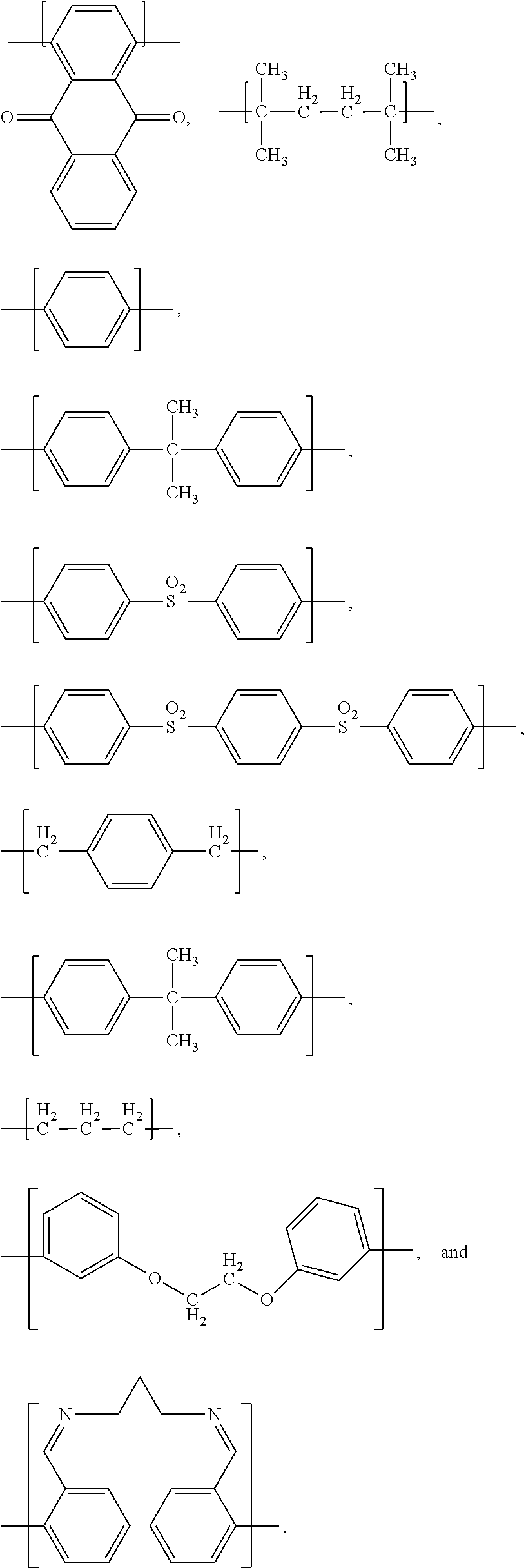
where R is selected from the group consisting of aryls (preferably C6-C12) and alkyls (preferably C1-C18, and more preferably C1-C10), each X is individually selected from the group consisting of: alkyls (preferably C1-C18, and more preferably C1-C10); alkoxys (preferably C1-C18, and more preferably C1-C10); carboxys; and combinations of two or more of the foregoing, and n is 2-6. The most preferred vinyl ether crosslinkers include those selected from the group consisting of ethylene glycol vinyl ether, trimethylolpropane trivinyl ether, 1,4-cyclohexane dimethanol divinyl ether, and mixtures thereof. Another preferred vinyl ether crosslinker has a formula selected from the group consisting of

where each of R1 and R2 is individually selected from the group consisting of functional moieties of diols, including aliphatic (preferably C1-C12) diols, aromatic (preferably C4-C12) diols, and heterocyclic diols). Preferred diols include those selected from the group consisting of bisphenols.
where R5 is an alkyl group (substituted or unsubstituted, preferably C1-C12, and more preferably C1-C6), and Ar is an aryl group (substituted or unsubstituted, preferably at least C4, more preferably C4-C12, and even more preferably C6-C10).


would be considered a functional moiety of bisphenol A, with the hydrogen atoms from each of the —OH groups originally present in the compound having been removed so that the oxygen atoms can bond with another compound or moiety.
where X1 is selected from the group consisting of functional moieties of diols and dioximes. Preferred diols include aliphatic (preferably C1-C12) diols, aromatic (preferably C4-C12) diols, and heterocyclic diols. Particularly preferred diols include those selected from the group consisting of the bisphenols. Preferred dioximes include aliphatic (preferably C1-C12) dioximes, aromatic (preferably C4-C12) dioximes, and heterocyclic dioximes. Particularly preferred dioximes include those derived from the condensation of an aliphatic diamine (NH2-carbon chain-NH2) and substituted or unsubstituted hydroxybenzaldehydes and hydroxyacetyl benzenes. One particularly preferred example is 1,4-diacetyl benzene dioxime.

where each of R3 and R4 is individually selected from the group consisting of substituted and unsubstituted aryls (preferably at least C4, more preferably C4-C12, and even more preferably C6-C10), and alkyls (preferably C1-C12, and more preferably C1-C6).
| TABLE I | |||||
| n at | k at | n at | |||
| 193 nm | 193 nm | 633 nm | Thickness (Å) | Cauchy A | Cauchy B |
| 1.6857 | 0.052 | 1.5 | 1410 | 1.4879 | 0.0049777 |
2. Preparation of Chromophore A

4. Preparation of
| TABLE II |
| Bottom |
| Thickness after | Thickness after | |||||
| Initial | Thickness | Exposure, PEB | % | Development | ||
| Thickness | after 20 s | % EL | and Development | change, | (Å) (no | % change, |
| (Å) | EL rinse (Å) | strip | (Å) | exposed | exposure) | unexposed |
| 758 | 773 | 1.6 | 0 | 100 | 770 | 0.39 |
| TABLE III |
| Bottom |
| Thickness | Thickness After | Thickness After | ||||
| Initial | After 20-s | Exposure, PEB, | % | Development | ||
| Thickness | EL Rinse | % EL | and Development | Change, | (unexposed) | % Change, |
| (Å) | (Å) | Strip | (Å) | Exposed | (Å) | Unexposed |
| 592 | 599 | 1.18 | 0 | 100 | 602 | 0.50 |
Claims (20)
Priority Applications (6)
| Application Number | Priority Date | Filing Date | Title |
|---|---|---|---|
| US11/839,317 US7914974B2 (en) | 2006-08-18 | 2007-08-15 | Anti-reflective imaging layer for multiple patterning process |
| KR1020097005529A KR101506353B1 (en) | 2006-08-18 | 2007-08-16 | Anti-reflective imaging layer for multiple patterning process |
| PCT/US2007/076078 WO2008022245A1 (en) | 2006-08-18 | 2007-08-16 | Anti-reflective imaging layer for multiple patterning process |
| EP07814157.9A EP2070107B1 (en) | 2006-08-18 | 2007-08-16 | Anti-reflective imaging layer for multiple patterning process |
| JP2009524799A JP5070287B2 (en) | 2006-08-18 | 2007-08-16 | Antireflective imaging layer for multiple patterning processes |
| TW096130672A TWI453792B (en) | 2006-08-18 | 2007-08-20 | Anti-reflective imaging layer for multiple patterning process |
Applications Claiming Priority (2)
| Application Number | Priority Date | Filing Date | Title |
|---|---|---|---|
| US82282306P | 2006-08-18 | 2006-08-18 | |
| US11/839,317 US7914974B2 (en) | 2006-08-18 | 2007-08-15 | Anti-reflective imaging layer for multiple patterning process |
Publications (2)
| Publication Number | Publication Date |
|---|---|
| US20080044772A1 US20080044772A1 (en) | 2008-02-21 |
| US7914974B2 true US7914974B2 (en) | 2011-03-29 |
Family
ID=39082361
Family Applications (1)
| Application Number | Title | Priority Date | Filing Date |
|---|---|---|---|
| US11/839,317 Active 2029-03-05 US7914974B2 (en) | 2006-08-18 | 2007-08-15 | Anti-reflective imaging layer for multiple patterning process |
Country Status (6)
| Country | Link |
|---|---|
| US (1) | US7914974B2 (en) |
| EP (1) | EP2070107B1 (en) |
| JP (1) | JP5070287B2 (en) |
| KR (1) | KR101506353B1 (en) |
| TW (1) | TWI453792B (en) |
| WO (1) | WO2008022245A1 (en) |
Cited By (4)
| Publication number | Priority date | Publication date | Assignee | Title |
|---|---|---|---|---|
| US20120073751A1 (en) * | 2008-05-09 | 2012-03-29 | Norikazu Mizuno | Manufacturing method of semiconductor device, and semiconductor device |
| US20120092632A1 (en) * | 2010-04-01 | 2012-04-19 | The Regents Of The University Of Colorado, A Body Corporate | Diffraction unlimited photolithography |
| US8877430B2 (en) | 2010-08-05 | 2014-11-04 | Brewer Science Inc. | Methods of producing structures using a developer-soluble layer with multilayer technology |
| US9960038B2 (en) | 2010-12-27 | 2018-05-01 | Brewer Science, Inc. | Processes to pattern small features for advanced patterning needs |
Families Citing this family (12)
| Publication number | Priority date | Publication date | Assignee | Title |
|---|---|---|---|---|
| US20050255410A1 (en) * | 2004-04-29 | 2005-11-17 | Guerrero Douglas J | Anti-reflective coatings using vinyl ether crosslinkers |
| US8133659B2 (en) | 2008-01-29 | 2012-03-13 | Brewer Science Inc. | On-track process for patterning hardmask by multiple dark field exposures |
| WO2009132023A2 (en) * | 2008-04-23 | 2009-10-29 | Brewer Science Inc. | Photosensitive hardmask for microlithography |
| US9640396B2 (en) | 2009-01-07 | 2017-05-02 | Brewer Science Inc. | Spin-on spacer materials for double- and triple-patterning lithography |
| JP2010278204A (en) * | 2009-05-28 | 2010-12-09 | Oki Semiconductor Co Ltd | Method for forming resist pattern |
| US7989346B2 (en) * | 2009-07-27 | 2011-08-02 | Adam Letize | Surface treatment of silicon |
| US8632948B2 (en) * | 2009-09-30 | 2014-01-21 | Az Electronic Materials Usa Corp. | Positive-working photoimageable bottom antireflective coating |
| US8440523B1 (en) * | 2011-12-07 | 2013-05-14 | International Business Machines Corporation | Micromechanical device and methods to fabricate same using hard mask resistant to structure release etch |
| JP6449145B2 (en) * | 2012-04-23 | 2019-01-09 | ブルーワー サイエンス アイ エヌ シー. | Photosensitive, developer-soluble bottom antireflection film material |
| JP6175226B2 (en) * | 2012-09-28 | 2017-08-02 | 富士フイルム株式会社 | Pattern forming method, actinic ray-sensitive or radiation-sensitive resin composition for semiconductor production, and method for producing electronic device |
| EP3015469B1 (en) | 2014-10-30 | 2018-12-19 | Idemitsu Kosan Co., Ltd. | 5-(benzimidazol-2-yl)benzimidazo[1,2-a]benzimidazoles for electronic applications |
| EP3721211A4 (en) | 2017-12-06 | 2021-08-18 | California Institute of Technology | System for analyzing a test sample and method therefor |
Citations (189)
| Publication number | Priority date | Publication date | Assignee | Title |
|---|---|---|---|---|
| US3345210A (en) | 1964-08-26 | 1967-10-03 | Motorola Inc | Method of applying an ohmic contact to thin film passivated resistors |
| US3561962A (en) | 1966-09-01 | 1971-02-09 | Xerox Corp | Method of image reproduction by photo-polymerization and blushing |
| US3615615A (en) | 1970-04-13 | 1971-10-26 | Eastman Kodak Co | Photographic emulsions including reactive quaternary salts |
| US3629036A (en) | 1969-02-14 | 1971-12-21 | Shipley Co | The method coating of photoresist on circuit boards |
| US3682641A (en) | 1970-03-23 | 1972-08-08 | Du Pont | Photoresist developer extender baths containing polyoxyalkylene ethers and esters and process of use |
| US3833374A (en) | 1970-07-14 | 1974-09-03 | Metalphoto Corp | Coloring of anodized aluminum |
| US3856751A (en) | 1972-06-14 | 1974-12-24 | Eastman Kodak Co | Diacid-xanthylium ion polyester and photographic element comprised thereof |
| US3873361A (en) | 1973-11-29 | 1975-03-25 | Ibm | Method of depositing thin film utilizing a lift-off mask |
| US3894163A (en) | 1971-03-08 | 1975-07-08 | Western Electric Co | Additives to negative photoresists which increase the sensitivity thereof |
| US3976524A (en) | 1974-06-17 | 1976-08-24 | Ibm Corporation | Planarization of integrated circuit surfaces through selective photoresist masking |
| US4137365A (en) | 1975-11-21 | 1979-01-30 | Nasa | Oxygen post-treatment of plastic surfaces coated with plasma polymerized silicon-containing monomers |
| US4175175A (en) | 1963-07-16 | 1979-11-20 | Union Carbide Corporation | Polyarylene polyethers |
| US4244799A (en) | 1978-09-11 | 1981-01-13 | Bell Telephone Laboratories, Incorporated | Fabrication of integrated circuits utilizing thick high-resolution patterns |
| US4320224A (en) | 1977-09-07 | 1982-03-16 | Imperial Chemical Industries Limited | Thermoplastic aromatic polyetherketones |
| US4346163A (en) | 1977-11-17 | 1982-08-24 | Matsushita Electric Industrial Co. Ltd. | Resist for use in forming a positive pattern with a radiation and process for forming a positive pattern with radiation |
| US4369090A (en) | 1980-11-06 | 1983-01-18 | Texas Instruments Incorporated | Process for etching sloped vias in polyimide insulators |
| US4397722A (en) | 1981-12-31 | 1983-08-09 | International Business Machines Corporation | Polymers from aromatic silanes and process for their preparation |
| US4430419A (en) | 1981-01-22 | 1984-02-07 | Nippon Telegraph & Telephone Public Corporation | Positive resist and method for manufacturing a pattern thereof |
| US4526856A (en) | 1983-05-23 | 1985-07-02 | Allied Corporation | Low striation positive diazoketone resist composition with cyclic ketone(s) and aliphatic alcohol as solvents |
| US4568631A (en) * | 1984-04-30 | 1986-02-04 | International Business Machines Corporation | Process for delineating photoresist lines at pattern edges only using image reversal composition with diazoquinone |
| US4578328A (en) | 1984-07-09 | 1986-03-25 | General Electric Company | Photopatternable polyimide compositions and method for making |
| US4647517A (en) | 1984-07-07 | 1987-03-03 | Licentia Patent-Verwaltungs-Gmbh | Mask for X-ray lithography |
| US4683024A (en) | 1985-02-04 | 1987-07-28 | American Telephone And Telegraph Company, At&T Bell Laboratories | Device fabrication method using spin-on glass resins |
| US4732841A (en) | 1986-03-24 | 1988-03-22 | Fairchild Semiconductor Corporation | Tri-level resist process for fine resolution photolithography |
| US4738916A (en) | 1984-06-11 | 1988-04-19 | Nippon Telegraph And Telephone Corp. | Intermediate layer material of three-layer resist system |
| US4742152A (en) | 1986-05-27 | 1988-05-03 | United Technologies Corporation | High temperature fluorinated polyimides |
| US4803147A (en) | 1987-11-24 | 1989-02-07 | Hoechst Celanese Corporation | Photosensitive polyimide polymer compositions |
| US4808513A (en) | 1987-04-06 | 1989-02-28 | Morton Thiokol, Inc. | Method of developing a high contrast, positive photoresist using a developer containing alkanolamine |
| US4845265A (en) | 1988-02-29 | 1989-07-04 | Allied-Signal Inc. | Polyfunctional vinyl ether terminated ester oligomers |
| US4891303A (en) | 1988-05-26 | 1990-01-02 | Texas Instruments Incorporated | Trilayer microlithographic process using a silicon-based resist as the middle layer |
| US4910122A (en) | 1982-09-30 | 1990-03-20 | Brewer Science, Inc. | Anti-reflective coating |
| US4927736A (en) | 1987-07-21 | 1990-05-22 | Hoechst Celanese Corporation | Hydroxy polyimides and high temperature positive photoresists therefrom |
| US4996247A (en) | 1984-02-10 | 1991-02-26 | General Electric Company | Enhancing color stability to sterilizing radiation of polymer compositions |
| US5057399A (en) | 1989-03-31 | 1991-10-15 | Tony Flaim | Method for making polyimide microlithographic compositions soluble in alkaline media |
| US5066566A (en) | 1990-07-31 | 1991-11-19 | At&T Bell Laboratories | Resist materials |
| US5089593A (en) | 1988-06-28 | 1992-02-18 | Amoco Corporation | Polyimide containing 4,4'-bis(4-amino-2-trifluoromethylphenoxy)-biphenyl moieties |
| US5091047A (en) | 1986-09-11 | 1992-02-25 | National Semiconductor Corp. | Plasma etching using a bilayer mask |
| US5106718A (en) | 1988-10-20 | 1992-04-21 | Ciba-Geigy Corporation | Positive photoresist composition containing alkali-soluble phenolic resin, photosensitive quinonediazide compound and sulfonyl containing compound |
| US5126231A (en) | 1990-02-26 | 1992-06-30 | Applied Materials, Inc. | Process for multi-layer photoresist etching with minimal feature undercut and unchanging photoresist load during etch |
| US5137780A (en) | 1987-10-16 | 1992-08-11 | The Curators Of The University Of Missouri | Article having a composite insulative coating |
| US5169494A (en) | 1989-03-27 | 1992-12-08 | Matsushita Electric Industrial Co., Ltd. | Fine pattern forming method |
| US5198153A (en) | 1989-05-26 | 1993-03-30 | International Business Machines Corporation | Electrically conductive polymeric |
| US5246782A (en) | 1990-12-10 | 1993-09-21 | The Dow Chemical Company | Laminates of polymers having perfluorocyclobutane rings and polymers containing perfluorocyclobutane rings |
| US5302548A (en) | 1987-07-31 | 1994-04-12 | Kabushiki Kaisha Toshiba | Semiconductor device manufacturing method |
| US5304626A (en) | 1988-06-28 | 1994-04-19 | Amoco Corporation | Polyimide copolymers containing 3,3',4,4'-tetracarboxybiphenyl dianhydride (BPDA) moieties |
| US5336925A (en) | 1988-11-07 | 1994-08-09 | Brewer Science, Inc. | Positive working polyamic acid/imide photoresist compositions and their use as dielectrics |
| US5340684A (en) | 1989-12-07 | 1994-08-23 | Kabushiki Kaisha Toshiba | Photosensitive composition and resin-encapsulated semiconductor device |
| US5370969A (en) | 1992-07-28 | 1994-12-06 | Sharp Kabushiki Kaisha | Trilayer lithographic process |
| US5397684A (en) | 1993-04-27 | 1995-03-14 | International Business Machines Corporation | Antireflective polyimide dielectric for photolithography |
| US5403438A (en) | 1991-01-10 | 1995-04-04 | Fujitsu Limited | Process for forming pattern |
| US5443941A (en) | 1993-03-01 | 1995-08-22 | National Semiconductor Corporation | Plasma polymer antireflective coating |
| GB2288184A (en) | 1994-03-31 | 1995-10-11 | Catalysts & Chem Ind Co | Coating composition |
| US5542971A (en) | 1994-12-01 | 1996-08-06 | Pitney Bowes | Bar codes using luminescent invisible inks |
| US5545588A (en) | 1995-05-05 | 1996-08-13 | Taiwan Semiconductor Manufacturing Company | Method of using disposable hard mask for gate critical dimension control |
| US5554473A (en) | 1994-11-23 | 1996-09-10 | Mitsubishi Chemical America, Inc. | Photoreceptor having charge transport layers containing a copolycarbonate and layer containing same |
| US5607824A (en) | 1994-07-27 | 1997-03-04 | International Business Machines Corporation | Antireflective coating for microlithography |
| US5633210A (en) | 1996-04-29 | 1997-05-27 | Taiwan Semiconductor Manufacturing Company, Ltd. | Method for forming damage free patterned layers adjoining the edges of high step height apertures |
| US5632910A (en) | 1993-12-24 | 1997-05-27 | Sony Corporation | Multilayer resist pattern forming method |
| US5667940A (en) * | 1994-05-11 | 1997-09-16 | United Microelectronics Corporation | Process for creating high density integrated circuits utilizing double coating photoresist mask |
| US5688987A (en) | 1994-11-09 | 1997-11-18 | Brewer Science, Inc. | Non-subliming Mid-UV dyes and ultra-thin organic arcs having differential solubility |
| US5691101A (en) | 1994-03-15 | 1997-11-25 | Kabushiki Kaisha Toshiba | Photosensitive composition |
| US5739254A (en) | 1996-08-29 | 1998-04-14 | Xerox Corporation | Process for haloalkylation of high performance polymers |
| US5772925A (en) | 1994-06-29 | 1998-06-30 | Shin-Etsu Chemical Co., Ltd. | Anti-reflective coating composition |
| US5807790A (en) | 1996-05-07 | 1998-09-15 | Advanced Micro Devices, Inc. | Selective i-line BARL etch process |
| US5922503A (en) | 1996-03-06 | 1999-07-13 | Clariant Finance (Bvi) Limited | Process for obtaining a lift-off imaging profile |
| US5925578A (en) | 1995-12-29 | 1999-07-20 | Hyundai Electronics Industries Co., Ltd. | Method for forming fine patterns of a semiconductor device |
| US5939235A (en) | 1993-02-05 | 1999-08-17 | Fuji Photo Film Co., Ltd. | Positive-working light-sensitive composition |
| US5952448A (en) | 1996-12-31 | 1999-09-14 | Korea Research Institute Of Chemical Technology | Stable precursor of polyimide and a process for preparing the same |
| US5968324A (en) | 1995-12-05 | 1999-10-19 | Applied Materials, Inc. | Method and apparatus for depositing antireflective coating |
| US5972560A (en) | 1997-01-31 | 1999-10-26 | Shin-Etsu Chemical Co., Ltd. | High molecular weight silicone compound, chemically amplified positive resist composition and patterning method |
| US5998569A (en) | 1998-03-17 | 1999-12-07 | International Business Machines Corporation | Environmentally stable optical filter materials |
| US6015650A (en) | 1995-12-29 | 2000-01-18 | Hyundai Electronics Industries Co., Ltd. | Method for forming micro patterns of semiconductor devices |
| US6020269A (en) | 1998-12-02 | 2000-02-01 | Advanced Micro Devices, Inc. | Ultra-thin resist and nitride/oxide hard mask for metal etch |
| US6042997A (en) | 1996-06-11 | 2000-03-28 | Ibm Corporation | Copolymers and photoresist compositions comprising copolymer resin binder component |
| US6046112A (en) | 1998-12-14 | 2000-04-04 | Taiwan Semiconductor Manufacturing Company | Chemical mechanical polishing slurry |
| US6054254A (en) | 1997-07-03 | 2000-04-25 | Kabushiki Kaisha Toshiba | Composition for underlying film and method of forming a pattern using the film |
| US6063547A (en) | 1998-06-11 | 2000-05-16 | Chartered Semiconductor Manufacturing, Ltd. | Physical vapor deposition poly-p-phenylene sulfide film as a bottom anti-reflective coating on polysilicon |
| US6071662A (en) | 1998-07-23 | 2000-06-06 | Xerox Corporation | Imaging member with improved anti-curl backing layer |
| US6103456A (en) | 1998-07-22 | 2000-08-15 | Siemens Aktiengesellschaft | Prevention of photoresist poisoning from dielectric antireflective coating in semiconductor fabrication |
| US6110653A (en) | 1999-07-26 | 2000-08-29 | International Business Machines Corporation | Acid sensitive ARC and method of use |
| EP1033624A1 (en) | 1998-08-07 | 2000-09-06 | Clariant International Ltd. | Radiation-sensitive composition of chemical amplification type |
| US6121098A (en) | 1998-06-30 | 2000-09-19 | Infineon Technologies North America Corporation | Semiconductor manufacturing method |
| US6124077A (en) | 1997-09-05 | 2000-09-26 | Kansai Paint Co., Ltd. | Visible light-sensitive compositions and pattern formation process |
| US6127070A (en) | 1998-12-01 | 2000-10-03 | Advanced Micro Devices, Inc. | Thin resist with nitride hard mask for via etch application |
| US6136679A (en) | 1999-03-05 | 2000-10-24 | Taiwan Semiconductor Manufacturing Company | Gate micro-patterning process |
| US6136511A (en) | 1999-01-20 | 2000-10-24 | Micron Technology, Inc. | Method of patterning substrates using multilayer resist processing |
| US6156665A (en) | 1998-04-13 | 2000-12-05 | Lucent Technologies Inc. | Trilayer lift-off process for semiconductor device metallization |
| US6156658A (en) | 1998-12-02 | 2000-12-05 | Advanced Micro Devices, Inc. | Ultra-thin resist and silicon/oxide hard mask for metal etch |
| US6162580A (en) | 1992-07-22 | 2000-12-19 | Asahi Kasei Kogyo Kabushiki Kaisha | Photosensitive polyimide precursor compositions processable by exposure to short wavelength light |
| US6165695A (en) | 1998-12-01 | 2000-12-26 | Advanced Micro Devices, Inc. | Thin resist with amorphous silicon hard mask for via etch application |
| US6171763B1 (en) | 1998-12-02 | 2001-01-09 | Advanced Micro Devices, Inc. | Ultra-thin resist and oxide/nitride hard mask for metal etch |
| US6187509B1 (en) | 1997-10-07 | 2001-02-13 | Kansai Paint Co., Ltd. | Positive type electrodeposition photoresist compositions and pattern formation process |
| US6200907B1 (en) | 1998-12-02 | 2001-03-13 | Advanced Micro Devices, Inc. | Ultra-thin resist and barrier metal/oxide hard mask for metal etch |
| US6207238B1 (en) | 1998-12-16 | 2001-03-27 | Battelle Memorial Institute | Plasma enhanced chemical deposition for high and/or low index of refraction polymers |
| US6218292B1 (en) | 1997-12-18 | 2001-04-17 | Advanced Micro Devices, Inc. | Dual layer bottom anti-reflective coating |
| US6232386B1 (en) | 1997-02-26 | 2001-05-15 | Integument Technologies, Inc. | Polymer composites having an oxyhalo surface and methods for making same |
| US6251562B1 (en) | 1998-12-23 | 2001-06-26 | International Business Machines Corporation | Antireflective polymer and method of use |
| US6268282B1 (en) | 1998-09-03 | 2001-07-31 | Micron Technology, Inc. | Semiconductor processing methods of forming and utilizing antireflective material layers, and methods of forming transistor gate stacks |
| US6268108B1 (en) | 1997-07-16 | 2001-07-31 | Tokyo Ohka Kogyo Co., Ltd. | Composition for forming antireflective coating film and method for forming resist pattern using same |
| US6291145B1 (en) | 1997-03-07 | 2001-09-18 | Nikon Corporation | Image formation method with photosensitive material |
| US6306560B1 (en) | 1998-12-02 | 2001-10-23 | Advanced Micro Devices, Inc. | Ultra-thin resist and SiON/oxide hard mask for metal etch |
| US6309926B1 (en) | 1998-12-04 | 2001-10-30 | Advanced Micro Devices | Thin resist with nitride hard mask for gate etch application |
| US6309789B1 (en) | 1998-06-03 | 2001-10-30 | Clariant Finance (Bvi) Limited | Composition for reflection reducing coating |
| US6309955B1 (en) | 2001-02-16 | 2001-10-30 | Advanced Micro Devices, Inc. | Method for using a CVD organic barc as a hard mask during via etch |
| US6316165B1 (en) | 1999-03-08 | 2001-11-13 | Shipley Company, L.L.C. | Planarizing antireflective coating compositions |
| US6319649B1 (en) | 1994-10-13 | 2001-11-20 | Hitachi, Ltd. | Photosensitive resin composition and method of forming resist images |
| US6338936B1 (en) | 1998-02-02 | 2002-01-15 | Taiyo Ink Manufacturing Co., Ltd. | Photosensitive resin composition and method for formation of resist pattern by use thereof |
| US20020009599A1 (en) | 2000-01-26 | 2002-01-24 | Welch Cletus N. | Photochromic polyurethane coating and articles having such a coating |
| US20020031729A1 (en) | 2000-07-31 | 2002-03-14 | Shipley Company, L.L.C. | Antireflective coating compositions |
| US6359028B1 (en) | 1995-07-12 | 2002-03-19 | Mitsubishi Engineering-Plastics Corporation | Polycarbonate resin composition |
| US6361833B1 (en) | 1998-10-28 | 2002-03-26 | Henkel Corporation | Composition and process for treating metal surfaces |
| US6380611B1 (en) | 1998-09-03 | 2002-04-30 | Micron Technology, Inc. | Treatment for film surface to reduce photo footing |
| US6383952B1 (en) | 2001-02-28 | 2002-05-07 | Advanced Micro Devices, Inc. | RELACS process to double the frequency or pitch of small feature formation |
| US6391472B1 (en) | 1999-08-26 | 2002-05-21 | Brewer Science, Inc. | Fill material for dual damascene processes |
| US20020076642A1 (en) | 2000-09-19 | 2002-06-20 | Shipley Company, L.L.C. | Antireflective composition |
| US6410209B1 (en) | 1998-09-15 | 2002-06-25 | Shipley Company, L.L.C. | Methods utilizing antireflective coating compositions with exposure under 200 nm |
| US6426125B1 (en) | 1999-03-17 | 2002-07-30 | General Electric Company | Multilayer article and method of making by ARC plasma deposition |
| US6428894B1 (en) | 1997-06-04 | 2002-08-06 | International Business Machines Corporation | Tunable and removable plasma deposited antireflective coatings |
| US20020106898A1 (en) | 2001-02-05 | 2002-08-08 | Ming-Sheng Tsai | Methods for removing silicon-oxy-nitride layer and wafer surface cleaning |
| US20020110665A1 (en) | 2000-04-24 | 2002-08-15 | Shipley Company, L.L.C. | Aperture fill |
| US6440640B1 (en) | 1998-12-01 | 2002-08-27 | Advanced Micro Devices, Inc. | Thin resist with transition metal hard mask for via etch application |
| US20020120070A1 (en) | 1998-12-31 | 2002-08-29 | Hyundai Electronics Industries Co., Ltd. | Anti reflective coating polymers and the preparation method thereof |
| US20020120091A1 (en) | 2001-02-16 | 2002-08-29 | Lisa Scott | Poly amic acid system for polyimides |
| US6451498B1 (en) | 1998-05-28 | 2002-09-17 | Atotech Deutschland Gmbh | Photosensitive composition |
| US6455416B1 (en) | 2000-10-24 | 2002-09-24 | Advanced Micro Devices, Inc. | Developer soluble dyed BARC for dual damascene process |
| US6458509B1 (en) | 1999-04-30 | 2002-10-01 | Toagosei Co., Ltd. | Resist compositions |
| US6458705B1 (en) | 2001-06-06 | 2002-10-01 | United Microelectronics Corp. | Method for forming via-first dual damascene interconnect structure |
| US20020160211A1 (en) | 2000-08-04 | 2002-10-31 | Tomoharu Kurita | Flexible metal-clad laminate and process for preparing the same |
| US6488509B1 (en) | 2002-01-23 | 2002-12-03 | Taiwan Semiconductor Manufacturing Company | Plug filling for dual-damascene process |
| US6487879B1 (en) | 1997-03-07 | 2002-12-03 | Corning Incorporated | Method of making titania-doped fused silica |
| US20020182874A1 (en) | 2001-06-01 | 2002-12-05 | Chih-Jung Wang | Method for forming hybrid low-k film stack to avoid thermal stress effect |
| US6509137B1 (en) | 2000-02-10 | 2003-01-21 | Winbond Electronics Corp. | Multilayer photoresist process in photolithography |
| US20030017688A1 (en) | 2001-07-20 | 2003-01-23 | United Microelectronics Corporation | Method for reducing hole defects in the polysilicon layer |
| US20030040179A1 (en) | 2001-08-24 | 2003-02-27 | Thakar Gautam V. | Polysilicon processing using an anti-reflective dual layer hardmask for 193 nm lithography |
| US20030049566A1 (en) | 2000-02-22 | 2003-03-13 | Sabnis Ram W. | Organic polymeric antireflective coatings deposited by chemical vapor deposition |
| US20030064608A1 (en) | 2001-02-02 | 2003-04-03 | Sabnis Ram W. | Polymeric antireflective coatings deposited by plasma enhanced chemical vapor deposition |
| US6558819B1 (en) | 1999-08-20 | 2003-05-06 | Fuji Photo Film Co., Ltd. | Arylsilane compound, light emitting device material and light emitting device by using the same |
| US6566280B1 (en) | 2002-08-26 | 2003-05-20 | Intel Corporation | Forming polymer features on a substrate |
| JP2003162065A (en) | 2001-11-26 | 2003-06-06 | Mitsubishi Electric Corp | Exposure system, mask for exposure, exposure method, display, and electronic parts |
| US6586560B1 (en) | 2001-09-18 | 2003-07-01 | Microchem Corp. | Alkaline soluble maleimide-containing polymers |
| JP2003183387A (en) | 2001-12-19 | 2003-07-03 | Central Glass Co Ltd | Fluorine-containing alicylic diamine and polymer using the same |
| US20030122269A1 (en) | 2001-05-29 | 2003-07-03 | Essilor International Compagnie Generale D'optique | Method for forming on-site a coated optical article |
| US20030129531A1 (en) | 2002-01-09 | 2003-07-10 | Oberlander Joseph E. | Positive-working photoimageable bottom antireflective coating |
| US20030129547A1 (en) | 2002-01-09 | 2003-07-10 | Neisser Mark O. | Process for producing an image using a first minimum bottom antireflective coating composition |
| US20030143404A1 (en) | 2001-11-01 | 2003-07-31 | Welch Cletus N. | Articles having a photochromic polymeric coating |
| US20030162120A1 (en) | 2002-02-16 | 2003-08-28 | Sang-Woong Yoon | Compositions for anti-reflective light absorbing layer and method for forming patterns in semiconductor device using the same |
| US6616692B1 (en) | 1999-04-30 | 2003-09-09 | Advanced Medical Optics, Inc. | Intraocular lens combinations |
| US20030194636A1 (en) | 2002-04-11 | 2003-10-16 | Wanat Stanley F. | Photoresist compositions comprising acetals and ketals as solvents |
| US6638853B1 (en) | 2002-07-03 | 2003-10-28 | Taiwan Semiconductor Manufacturing Co. Ltd. | Method for avoiding photoresist resist residue on semioconductor feature sidewalls |
| US20030215736A1 (en) | 2002-01-09 | 2003-11-20 | Oberlander Joseph E. | Negative-working photoimageable bottom antireflective coating |
| US20040010062A1 (en) | 2001-09-27 | 2004-01-15 | Byeong-In Ahn | Polyimide copolymer and methods for preparing the same |
| US6680252B2 (en) | 2001-05-15 | 2004-01-20 | United Microelectronics Corp. | Method for planarizing barc layer in dual damascene process |
| US20040018451A1 (en) | 2002-07-23 | 2004-01-29 | Samsung Electronics Co., Ltd. | Photoresist developer-soluble organic bottom antireflective composition and photolithography and etching process using the same |
| US20040053141A1 (en) * | 2002-09-16 | 2004-03-18 | Numerical Technologies, Inc. | Using second exposure to assist a PSM exposure in printing a tight space adjacent to large feature |
| US6709979B2 (en) | 2000-05-29 | 2004-03-23 | Sony Corporation | Method of manufacturing a semiconductor device |
| US20040058275A1 (en) | 2002-06-25 | 2004-03-25 | Brewer Science, Inc. | Wet-developable anti-reflective compositions |
| US20040077173A1 (en) | 2002-10-17 | 2004-04-22 | Swaminathan Sivakumar | Using water soluble bottom anti-reflective coating |
| US6740469B2 (en) | 2002-06-25 | 2004-05-25 | Brewer Science Inc. | Developer-soluble metal alkoxide coatings for microelectronic applications |
| US6767689B2 (en) | 2001-05-11 | 2004-07-27 | Shipley Company, L.L.C. | Antireflective coating compositions |
| US6803172B2 (en) | 2001-10-26 | 2004-10-12 | Hynix Semiconductor Inc. | Organic anti-reflective coating material and preparation thereof |
| US6803168B1 (en) | 1997-05-27 | 2004-10-12 | Clariant Finance (Bvi) Limited | Composition for anti-reflective coating or radiation absorbing coating and compounds used in the composition |
| US20040210034A1 (en) | 2002-01-17 | 2004-10-21 | Cox Robert Christian | Spin bowl compatible polyamic acids/imides as wet developable polymer binders for anti-reflective coatings |
| US20040220379A1 (en) | 2003-05-02 | 2004-11-04 | Park Seung Koo | Polyamic ester having moieties of electro optic and nonlinear optical compound in side chains as an electro optic and nonlinear optical polymer, manufacturing method therefor and film manufactured therefrom |
| EP1480081A2 (en) | 2003-05-22 | 2004-11-24 | Clariant International Ltd. | Use of water soluble negative tone photoresist for producing closely spaced contact holes |
| WO2004113417A1 (en) | 2003-05-23 | 2004-12-29 | Dow Corning Corporation | Siloxane resin-based anti-reflective coating composition having high wet etch rate |
| US6849293B2 (en) | 2002-05-02 | 2005-02-01 | Institute Of Microelectronics | Method to minimize iso-dense contact or via gap filling variation of polymeric materials in the spin coat process |
| US6852474B2 (en) | 2002-04-30 | 2005-02-08 | Brewer Science Inc. | Polymeric antireflective coatings deposited by plasma enhanced chemical vapor deposition |
| US6852473B2 (en) | 2000-01-12 | 2005-02-08 | Infineon Technologies Richmond, Lp | Anti-reflective coating conformality control |
| US20050074699A1 (en) | 2003-06-11 | 2005-04-07 | Sun Sam X. | Wet developable hard mask in conjunction with thin photoresist for micro photolithography |
| US6893702B2 (en) | 2000-05-29 | 2005-05-17 | Fujitsu Limited | Magnetic recording medium substrate, method of producing the same, and method of evaluating magnetic recording medium |
| US20050148170A1 (en) | 2003-10-15 | 2005-07-07 | Mandar Bhave | Developer-soluble materials and methods of using the same in via-first dual damascene applications |
| US6924228B2 (en) | 2003-03-06 | 2005-08-02 | Samsung Electronics Co., Ltd. | Method of forming a via contact structure using a dual damascene technique |
| US20050214674A1 (en) | 2004-03-25 | 2005-09-29 | Yu Sui | Positive-working photoimageable bottom antireflective coating |
| US20050255410A1 (en) * | 2004-04-29 | 2005-11-17 | Guerrero Douglas J | Anti-reflective coatings using vinyl ether crosslinkers |
| US6976904B2 (en) | 1998-07-09 | 2005-12-20 | Li Family Holdings, Ltd. | Chemical mechanical polishing slurry |
| US20060019455A1 (en) | 2004-07-26 | 2006-01-26 | Haowen Bu | Transistor fabrication methods using reduced width sidewall spacers |
| US7074527B2 (en) | 2003-09-23 | 2006-07-11 | Freescale Semiconductor, Inc. | Method for fabricating a mask using a hardmask and method for making a semiconductor device using the same |
| US20060160028A1 (en) * | 2005-01-17 | 2006-07-20 | Hyung-Rae Lee | Method of forming fine patterns of a semiconductor device |
| US7108958B2 (en) | 2002-07-31 | 2006-09-19 | Brewer Science Inc. | Photosensitive bottom anti-reflective coatings |
| US20070018286A1 (en) | 2005-07-14 | 2007-01-25 | Asml Netherlands B.V. | Substrate, lithographic multiple exposure method, machine readable medium |
| US20070196772A1 (en) | 2006-02-23 | 2007-08-23 | Hynix Semiconductor Inc. | Method for forming fine pattern of semiconductor device |
| US7265431B2 (en) | 2002-05-17 | 2007-09-04 | Intel Corporation | Imageable bottom anti-reflective coating for high resolution lithography |
| US20070207406A1 (en) | 2004-04-29 | 2007-09-06 | Guerrero Douglas J | Anti-reflective coatings using vinyl ether crosslinkers |
| US20070212649A1 (en) | 2006-03-07 | 2007-09-13 | Asml Netherlands B.V. | Method and system for enhanced lithographic patterning |
| US20070212654A1 (en) * | 2006-03-09 | 2007-09-13 | International Business Machines Corporation | Method for lithography for optimizing process conditions |
| EP1845416A2 (en) | 2006-04-11 | 2007-10-17 | Rohm and Haas Electronic Materials, L.L.C. | Coating compositions for photolithography |
| US20070264830A1 (en) | 2006-05-10 | 2007-11-15 | Lam Research Corporation | Pitch reduction |
| US20090111281A1 (en) | 2007-10-26 | 2009-04-30 | Christopher Dennis Bencher | Frequency doubling using a photo-resist template mask |
| EP1061560B1 (en) | 1999-06-11 | 2011-03-09 | Shipley Company LLC | Antireflective hard mask compositions |
Family Cites Families (4)
| Publication number | Priority date | Publication date | Assignee | Title |
|---|---|---|---|---|
| JPH04151155A (en) * | 1990-10-15 | 1992-05-25 | Seiko Epson Corp | Manufacture of semiconductor device |
| JPH05326358A (en) * | 1992-05-18 | 1993-12-10 | Sony Corp | Method for forming fine pattern |
| KR970071126A (en) * | 1996-04-01 | 1997-11-07 | 김광호 | Pattern formation method using dual photoresist |
| TW495839B (en) * | 2001-03-12 | 2002-07-21 | Nanya Technology Corp | Multiple exposure method |
-
2007
- 2007-08-15 US US11/839,317 patent/US7914974B2/en active Active
- 2007-08-16 WO PCT/US2007/076078 patent/WO2008022245A1/en active Application Filing
- 2007-08-16 KR KR1020097005529A patent/KR101506353B1/en active IP Right Grant
- 2007-08-16 JP JP2009524799A patent/JP5070287B2/en active Active
- 2007-08-16 EP EP07814157.9A patent/EP2070107B1/en active Active
- 2007-08-20 TW TW096130672A patent/TWI453792B/en active
Patent Citations (201)
| Publication number | Priority date | Publication date | Assignee | Title |
|---|---|---|---|---|
| US4175175A (en) | 1963-07-16 | 1979-11-20 | Union Carbide Corporation | Polyarylene polyethers |
| US3345210A (en) | 1964-08-26 | 1967-10-03 | Motorola Inc | Method of applying an ohmic contact to thin film passivated resistors |
| US3561962A (en) | 1966-09-01 | 1971-02-09 | Xerox Corp | Method of image reproduction by photo-polymerization and blushing |
| US3629036A (en) | 1969-02-14 | 1971-12-21 | Shipley Co | The method coating of photoresist on circuit boards |
| US3682641A (en) | 1970-03-23 | 1972-08-08 | Du Pont | Photoresist developer extender baths containing polyoxyalkylene ethers and esters and process of use |
| US3615615A (en) | 1970-04-13 | 1971-10-26 | Eastman Kodak Co | Photographic emulsions including reactive quaternary salts |
| US3833374A (en) | 1970-07-14 | 1974-09-03 | Metalphoto Corp | Coloring of anodized aluminum |
| US3894163A (en) | 1971-03-08 | 1975-07-08 | Western Electric Co | Additives to negative photoresists which increase the sensitivity thereof |
| US3856751A (en) | 1972-06-14 | 1974-12-24 | Eastman Kodak Co | Diacid-xanthylium ion polyester and photographic element comprised thereof |
| US3873361A (en) | 1973-11-29 | 1975-03-25 | Ibm | Method of depositing thin film utilizing a lift-off mask |
| US3976524A (en) | 1974-06-17 | 1976-08-24 | Ibm Corporation | Planarization of integrated circuit surfaces through selective photoresist masking |
| US4137365A (en) | 1975-11-21 | 1979-01-30 | Nasa | Oxygen post-treatment of plastic surfaces coated with plasma polymerized silicon-containing monomers |
| US4320224A (en) | 1977-09-07 | 1982-03-16 | Imperial Chemical Industries Limited | Thermoplastic aromatic polyetherketones |
| US4346163A (en) | 1977-11-17 | 1982-08-24 | Matsushita Electric Industrial Co. Ltd. | Resist for use in forming a positive pattern with a radiation and process for forming a positive pattern with radiation |
| US4244799A (en) | 1978-09-11 | 1981-01-13 | Bell Telephone Laboratories, Incorporated | Fabrication of integrated circuits utilizing thick high-resolution patterns |
| US4369090A (en) | 1980-11-06 | 1983-01-18 | Texas Instruments Incorporated | Process for etching sloped vias in polyimide insulators |
| US4430419A (en) | 1981-01-22 | 1984-02-07 | Nippon Telegraph & Telephone Public Corporation | Positive resist and method for manufacturing a pattern thereof |
| US4397722A (en) | 1981-12-31 | 1983-08-09 | International Business Machines Corporation | Polymers from aromatic silanes and process for their preparation |
| US4910122A (en) | 1982-09-30 | 1990-03-20 | Brewer Science, Inc. | Anti-reflective coating |
| US4526856A (en) | 1983-05-23 | 1985-07-02 | Allied Corporation | Low striation positive diazoketone resist composition with cyclic ketone(s) and aliphatic alcohol as solvents |
| US4996247A (en) | 1984-02-10 | 1991-02-26 | General Electric Company | Enhancing color stability to sterilizing radiation of polymer compositions |
| US4568631A (en) * | 1984-04-30 | 1986-02-04 | International Business Machines Corporation | Process for delineating photoresist lines at pattern edges only using image reversal composition with diazoquinone |
| US4738916A (en) | 1984-06-11 | 1988-04-19 | Nippon Telegraph And Telephone Corp. | Intermediate layer material of three-layer resist system |
| US4647517A (en) | 1984-07-07 | 1987-03-03 | Licentia Patent-Verwaltungs-Gmbh | Mask for X-ray lithography |
| US4578328A (en) | 1984-07-09 | 1986-03-25 | General Electric Company | Photopatternable polyimide compositions and method for making |
| US4683024A (en) | 1985-02-04 | 1987-07-28 | American Telephone And Telegraph Company, At&T Bell Laboratories | Device fabrication method using spin-on glass resins |
| US4732841A (en) | 1986-03-24 | 1988-03-22 | Fairchild Semiconductor Corporation | Tri-level resist process for fine resolution photolithography |
| US4742152A (en) | 1986-05-27 | 1988-05-03 | United Technologies Corporation | High temperature fluorinated polyimides |
| US5091047A (en) | 1986-09-11 | 1992-02-25 | National Semiconductor Corp. | Plasma etching using a bilayer mask |
| US4808513A (en) | 1987-04-06 | 1989-02-28 | Morton Thiokol, Inc. | Method of developing a high contrast, positive photoresist using a developer containing alkanolamine |
| US4927736A (en) | 1987-07-21 | 1990-05-22 | Hoechst Celanese Corporation | Hydroxy polyimides and high temperature positive photoresists therefrom |
| US5302548A (en) | 1987-07-31 | 1994-04-12 | Kabushiki Kaisha Toshiba | Semiconductor device manufacturing method |
| US5137780A (en) | 1987-10-16 | 1992-08-11 | The Curators Of The University Of Missouri | Article having a composite insulative coating |
| US4803147A (en) | 1987-11-24 | 1989-02-07 | Hoechst Celanese Corporation | Photosensitive polyimide polymer compositions |
| US4845265A (en) | 1988-02-29 | 1989-07-04 | Allied-Signal Inc. | Polyfunctional vinyl ether terminated ester oligomers |
| US4891303A (en) | 1988-05-26 | 1990-01-02 | Texas Instruments Incorporated | Trilayer microlithographic process using a silicon-based resist as the middle layer |
| US5089593A (en) | 1988-06-28 | 1992-02-18 | Amoco Corporation | Polyimide containing 4,4'-bis(4-amino-2-trifluoromethylphenoxy)-biphenyl moieties |
| US5304626A (en) | 1988-06-28 | 1994-04-19 | Amoco Corporation | Polyimide copolymers containing 3,3',4,4'-tetracarboxybiphenyl dianhydride (BPDA) moieties |
| US5106718A (en) | 1988-10-20 | 1992-04-21 | Ciba-Geigy Corporation | Positive photoresist composition containing alkali-soluble phenolic resin, photosensitive quinonediazide compound and sulfonyl containing compound |
| US5336925A (en) | 1988-11-07 | 1994-08-09 | Brewer Science, Inc. | Positive working polyamic acid/imide photoresist compositions and their use as dielectrics |
| US5169494A (en) | 1989-03-27 | 1992-12-08 | Matsushita Electric Industrial Co., Ltd. | Fine pattern forming method |
| US5057399A (en) | 1989-03-31 | 1991-10-15 | Tony Flaim | Method for making polyimide microlithographic compositions soluble in alkaline media |
| US5198153A (en) | 1989-05-26 | 1993-03-30 | International Business Machines Corporation | Electrically conductive polymeric |
| US5340684A (en) | 1989-12-07 | 1994-08-23 | Kabushiki Kaisha Toshiba | Photosensitive composition and resin-encapsulated semiconductor device |
| US5126231A (en) | 1990-02-26 | 1992-06-30 | Applied Materials, Inc. | Process for multi-layer photoresist etching with minimal feature undercut and unchanging photoresist load during etch |
| US5066566A (en) | 1990-07-31 | 1991-11-19 | At&T Bell Laboratories | Resist materials |
| US5246782A (en) | 1990-12-10 | 1993-09-21 | The Dow Chemical Company | Laminates of polymers having perfluorocyclobutane rings and polymers containing perfluorocyclobutane rings |
| US5403438A (en) | 1991-01-10 | 1995-04-04 | Fujitsu Limited | Process for forming pattern |
| US6162580A (en) | 1992-07-22 | 2000-12-19 | Asahi Kasei Kogyo Kabushiki Kaisha | Photosensitive polyimide precursor compositions processable by exposure to short wavelength light |
| US5370969A (en) | 1992-07-28 | 1994-12-06 | Sharp Kabushiki Kaisha | Trilayer lithographic process |
| US5939235A (en) | 1993-02-05 | 1999-08-17 | Fuji Photo Film Co., Ltd. | Positive-working light-sensitive composition |
| US5443941A (en) | 1993-03-01 | 1995-08-22 | National Semiconductor Corporation | Plasma polymer antireflective coating |
| US5397684A (en) | 1993-04-27 | 1995-03-14 | International Business Machines Corporation | Antireflective polyimide dielectric for photolithography |
| US5632910A (en) | 1993-12-24 | 1997-05-27 | Sony Corporation | Multilayer resist pattern forming method |
| US5691101A (en) | 1994-03-15 | 1997-11-25 | Kabushiki Kaisha Toshiba | Photosensitive composition |
| GB2288184A (en) | 1994-03-31 | 1995-10-11 | Catalysts & Chem Ind Co | Coating composition |
| US5667940A (en) * | 1994-05-11 | 1997-09-16 | United Microelectronics Corporation | Process for creating high density integrated circuits utilizing double coating photoresist mask |
| US5772925A (en) | 1994-06-29 | 1998-06-30 | Shin-Etsu Chemical Co., Ltd. | Anti-reflective coating composition |
| US5607824A (en) | 1994-07-27 | 1997-03-04 | International Business Machines Corporation | Antireflective coating for microlithography |
| US6319649B1 (en) | 1994-10-13 | 2001-11-20 | Hitachi, Ltd. | Photosensitive resin composition and method of forming resist images |
| US5892096A (en) | 1994-11-09 | 1999-04-06 | Brewer Science, Inc. | Non-subliming mid-UV dyes and ultra-thin organic arcs having differential solubility |
| US5688987A (en) | 1994-11-09 | 1997-11-18 | Brewer Science, Inc. | Non-subliming Mid-UV dyes and ultra-thin organic arcs having differential solubility |
| US5554473A (en) | 1994-11-23 | 1996-09-10 | Mitsubishi Chemical America, Inc. | Photoreceptor having charge transport layers containing a copolycarbonate and layer containing same |
| US5542971A (en) | 1994-12-01 | 1996-08-06 | Pitney Bowes | Bar codes using luminescent invisible inks |
| US5545588A (en) | 1995-05-05 | 1996-08-13 | Taiwan Semiconductor Manufacturing Company | Method of using disposable hard mask for gate critical dimension control |
| US6359028B1 (en) | 1995-07-12 | 2002-03-19 | Mitsubishi Engineering-Plastics Corporation | Polycarbonate resin composition |
| US5968324A (en) | 1995-12-05 | 1999-10-19 | Applied Materials, Inc. | Method and apparatus for depositing antireflective coating |
| US5925578A (en) | 1995-12-29 | 1999-07-20 | Hyundai Electronics Industries Co., Ltd. | Method for forming fine patterns of a semiconductor device |
| US6015650A (en) | 1995-12-29 | 2000-01-18 | Hyundai Electronics Industries Co., Ltd. | Method for forming micro patterns of semiconductor devices |
| US5922503A (en) | 1996-03-06 | 1999-07-13 | Clariant Finance (Bvi) Limited | Process for obtaining a lift-off imaging profile |
| US5633210A (en) | 1996-04-29 | 1997-05-27 | Taiwan Semiconductor Manufacturing Company, Ltd. | Method for forming damage free patterned layers adjoining the edges of high step height apertures |
| US5807790A (en) | 1996-05-07 | 1998-09-15 | Advanced Micro Devices, Inc. | Selective i-line BARL etch process |
| US6042997A (en) | 1996-06-11 | 2000-03-28 | Ibm Corporation | Copolymers and photoresist compositions comprising copolymer resin binder component |
| US5739254A (en) | 1996-08-29 | 1998-04-14 | Xerox Corporation | Process for haloalkylation of high performance polymers |
| US5952448A (en) | 1996-12-31 | 1999-09-14 | Korea Research Institute Of Chemical Technology | Stable precursor of polyimide and a process for preparing the same |
| US5972560A (en) | 1997-01-31 | 1999-10-26 | Shin-Etsu Chemical Co., Ltd. | High molecular weight silicone compound, chemically amplified positive resist composition and patterning method |
| US6232386B1 (en) | 1997-02-26 | 2001-05-15 | Integument Technologies, Inc. | Polymer composites having an oxyhalo surface and methods for making same |
| US6487879B1 (en) | 1997-03-07 | 2002-12-03 | Corning Incorporated | Method of making titania-doped fused silica |
| US6291145B1 (en) | 1997-03-07 | 2001-09-18 | Nikon Corporation | Image formation method with photosensitive material |
| US6803168B1 (en) | 1997-05-27 | 2004-10-12 | Clariant Finance (Bvi) Limited | Composition for anti-reflective coating or radiation absorbing coating and compounds used in the composition |
| US6428894B1 (en) | 1997-06-04 | 2002-08-06 | International Business Machines Corporation | Tunable and removable plasma deposited antireflective coatings |
| US6054254A (en) | 1997-07-03 | 2000-04-25 | Kabushiki Kaisha Toshiba | Composition for underlying film and method of forming a pattern using the film |
| US6268108B1 (en) | 1997-07-16 | 2001-07-31 | Tokyo Ohka Kogyo Co., Ltd. | Composition for forming antireflective coating film and method for forming resist pattern using same |
| US6124077A (en) | 1997-09-05 | 2000-09-26 | Kansai Paint Co., Ltd. | Visible light-sensitive compositions and pattern formation process |
| US6187509B1 (en) | 1997-10-07 | 2001-02-13 | Kansai Paint Co., Ltd. | Positive type electrodeposition photoresist compositions and pattern formation process |
| US6218292B1 (en) | 1997-12-18 | 2001-04-17 | Advanced Micro Devices, Inc. | Dual layer bottom anti-reflective coating |
| US6338936B1 (en) | 1998-02-02 | 2002-01-15 | Taiyo Ink Manufacturing Co., Ltd. | Photosensitive resin composition and method for formation of resist pattern by use thereof |
| US6576409B2 (en) | 1998-02-02 | 2003-06-10 | Taiyo Ink Manufacturing Co., Ltd. | Photosensitive resin composition and method for formation of resist pattern by use thereof |
| US5998569A (en) | 1998-03-17 | 1999-12-07 | International Business Machines Corporation | Environmentally stable optical filter materials |
| US6156665A (en) | 1998-04-13 | 2000-12-05 | Lucent Technologies Inc. | Trilayer lift-off process for semiconductor device metallization |
| US6451498B1 (en) | 1998-05-28 | 2002-09-17 | Atotech Deutschland Gmbh | Photosensitive composition |
| US6309789B1 (en) | 1998-06-03 | 2001-10-30 | Clariant Finance (Bvi) Limited | Composition for reflection reducing coating |
| US6063547A (en) | 1998-06-11 | 2000-05-16 | Chartered Semiconductor Manufacturing, Ltd. | Physical vapor deposition poly-p-phenylene sulfide film as a bottom anti-reflective coating on polysilicon |
| US6121098A (en) | 1998-06-30 | 2000-09-19 | Infineon Technologies North America Corporation | Semiconductor manufacturing method |
| US6976904B2 (en) | 1998-07-09 | 2005-12-20 | Li Family Holdings, Ltd. | Chemical mechanical polishing slurry |
| US6103456A (en) | 1998-07-22 | 2000-08-15 | Siemens Aktiengesellschaft | Prevention of photoresist poisoning from dielectric antireflective coating in semiconductor fabrication |
| US6071662A (en) | 1998-07-23 | 2000-06-06 | Xerox Corporation | Imaging member with improved anti-curl backing layer |
| EP1033624A1 (en) | 1998-08-07 | 2000-09-06 | Clariant International Ltd. | Radiation-sensitive composition of chemical amplification type |
| US6268282B1 (en) | 1998-09-03 | 2001-07-31 | Micron Technology, Inc. | Semiconductor processing methods of forming and utilizing antireflective material layers, and methods of forming transistor gate stacks |
| US6380611B1 (en) | 1998-09-03 | 2002-04-30 | Micron Technology, Inc. | Treatment for film surface to reduce photo footing |
| US6410209B1 (en) | 1998-09-15 | 2002-06-25 | Shipley Company, L.L.C. | Methods utilizing antireflective coating compositions with exposure under 200 nm |
| US6602652B2 (en) | 1998-09-15 | 2003-08-05 | Shipley Company, L.L.C. | Antireflective coating compositions and exposure methods under 200 nm |
| US6361833B1 (en) | 1998-10-28 | 2002-03-26 | Henkel Corporation | Composition and process for treating metal surfaces |
| US6165695A (en) | 1998-12-01 | 2000-12-26 | Advanced Micro Devices, Inc. | Thin resist with amorphous silicon hard mask for via etch application |
| US6440640B1 (en) | 1998-12-01 | 2002-08-27 | Advanced Micro Devices, Inc. | Thin resist with transition metal hard mask for via etch application |
| US6127070A (en) | 1998-12-01 | 2000-10-03 | Advanced Micro Devices, Inc. | Thin resist with nitride hard mask for via etch application |
| US6200907B1 (en) | 1998-12-02 | 2001-03-13 | Advanced Micro Devices, Inc. | Ultra-thin resist and barrier metal/oxide hard mask for metal etch |
| US6156658A (en) | 1998-12-02 | 2000-12-05 | Advanced Micro Devices, Inc. | Ultra-thin resist and silicon/oxide hard mask for metal etch |
| US6020269A (en) | 1998-12-02 | 2000-02-01 | Advanced Micro Devices, Inc. | Ultra-thin resist and nitride/oxide hard mask for metal etch |
| US6171763B1 (en) | 1998-12-02 | 2001-01-09 | Advanced Micro Devices, Inc. | Ultra-thin resist and oxide/nitride hard mask for metal etch |
| US6306560B1 (en) | 1998-12-02 | 2001-10-23 | Advanced Micro Devices, Inc. | Ultra-thin resist and SiON/oxide hard mask for metal etch |
| US6309926B1 (en) | 1998-12-04 | 2001-10-30 | Advanced Micro Devices | Thin resist with nitride hard mask for gate etch application |
| US6046112A (en) | 1998-12-14 | 2000-04-04 | Taiwan Semiconductor Manufacturing Company | Chemical mechanical polishing slurry |
| US6207238B1 (en) | 1998-12-16 | 2001-03-27 | Battelle Memorial Institute | Plasma enhanced chemical deposition for high and/or low index of refraction polymers |
| US6251562B1 (en) | 1998-12-23 | 2001-06-26 | International Business Machines Corporation | Antireflective polymer and method of use |
| US20020120070A1 (en) | 1998-12-31 | 2002-08-29 | Hyundai Electronics Industries Co., Ltd. | Anti reflective coating polymers and the preparation method thereof |
| US6136511A (en) | 1999-01-20 | 2000-10-24 | Micron Technology, Inc. | Method of patterning substrates using multilayer resist processing |
| US6136679A (en) | 1999-03-05 | 2000-10-24 | Taiwan Semiconductor Manufacturing Company | Gate micro-patterning process |
| US6316165B1 (en) | 1999-03-08 | 2001-11-13 | Shipley Company, L.L.C. | Planarizing antireflective coating compositions |
| US6426125B1 (en) | 1999-03-17 | 2002-07-30 | General Electric Company | Multilayer article and method of making by ARC plasma deposition |
| US6616692B1 (en) | 1999-04-30 | 2003-09-09 | Advanced Medical Optics, Inc. | Intraocular lens combinations |
| US6458509B1 (en) | 1999-04-30 | 2002-10-01 | Toagosei Co., Ltd. | Resist compositions |
| EP1061560B1 (en) | 1999-06-11 | 2011-03-09 | Shipley Company LLC | Antireflective hard mask compositions |
| US6319651B1 (en) | 1999-07-26 | 2001-11-20 | International Business Machines Corporation | Acid sensitive ARC and method of use |
| US6110653A (en) | 1999-07-26 | 2000-08-29 | International Business Machines Corporation | Acid sensitive ARC and method of use |
| US6558819B1 (en) | 1999-08-20 | 2003-05-06 | Fuji Photo Film Co., Ltd. | Arylsilane compound, light emitting device material and light emitting device by using the same |
| US6391472B1 (en) | 1999-08-26 | 2002-05-21 | Brewer Science, Inc. | Fill material for dual damascene processes |
| US20020183426A1 (en) | 1999-08-26 | 2002-12-05 | Lamb James E. | Crosslinkable fill compositions for uniformly protecting via and contact holes |
| US6852473B2 (en) | 2000-01-12 | 2005-02-08 | Infineon Technologies Richmond, Lp | Anti-reflective coating conformality control |
| US20020009599A1 (en) | 2000-01-26 | 2002-01-24 | Welch Cletus N. | Photochromic polyurethane coating and articles having such a coating |
| US6509137B1 (en) | 2000-02-10 | 2003-01-21 | Winbond Electronics Corp. | Multilayer photoresist process in photolithography |
| US20030049566A1 (en) | 2000-02-22 | 2003-03-13 | Sabnis Ram W. | Organic polymeric antireflective coatings deposited by chemical vapor deposition |
| US20020110665A1 (en) | 2000-04-24 | 2002-08-15 | Shipley Company, L.L.C. | Aperture fill |
| US6893702B2 (en) | 2000-05-29 | 2005-05-17 | Fujitsu Limited | Magnetic recording medium substrate, method of producing the same, and method of evaluating magnetic recording medium |
| US6709979B2 (en) | 2000-05-29 | 2004-03-23 | Sony Corporation | Method of manufacturing a semiconductor device |
| US20020031729A1 (en) | 2000-07-31 | 2002-03-14 | Shipley Company, L.L.C. | Antireflective coating compositions |
| US20020160211A1 (en) | 2000-08-04 | 2002-10-31 | Tomoharu Kurita | Flexible metal-clad laminate and process for preparing the same |
| US20020076642A1 (en) | 2000-09-19 | 2002-06-20 | Shipley Company, L.L.C. | Antireflective composition |
| US6455416B1 (en) | 2000-10-24 | 2002-09-24 | Advanced Micro Devices, Inc. | Developer soluble dyed BARC for dual damascene process |
| US20030064608A1 (en) | 2001-02-02 | 2003-04-03 | Sabnis Ram W. | Polymeric antireflective coatings deposited by plasma enhanced chemical vapor deposition |
| US20020106898A1 (en) | 2001-02-05 | 2002-08-08 | Ming-Sheng Tsai | Methods for removing silicon-oxy-nitride layer and wafer surface cleaning |
| US20020120091A1 (en) | 2001-02-16 | 2002-08-29 | Lisa Scott | Poly amic acid system for polyimides |
| US6309955B1 (en) | 2001-02-16 | 2001-10-30 | Advanced Micro Devices, Inc. | Method for using a CVD organic barc as a hard mask during via etch |
| US6383952B1 (en) | 2001-02-28 | 2002-05-07 | Advanced Micro Devices, Inc. | RELACS process to double the frequency or pitch of small feature formation |
| US6767689B2 (en) | 2001-05-11 | 2004-07-27 | Shipley Company, L.L.C. | Antireflective coating compositions |
| US6680252B2 (en) | 2001-05-15 | 2004-01-20 | United Microelectronics Corp. | Method for planarizing barc layer in dual damascene process |
| US20030122269A1 (en) | 2001-05-29 | 2003-07-03 | Essilor International Compagnie Generale D'optique | Method for forming on-site a coated optical article |
| US20020182874A1 (en) | 2001-06-01 | 2002-12-05 | Chih-Jung Wang | Method for forming hybrid low-k film stack to avoid thermal stress effect |
| US6458705B1 (en) | 2001-06-06 | 2002-10-01 | United Microelectronics Corp. | Method for forming via-first dual damascene interconnect structure |
| US20030017688A1 (en) | 2001-07-20 | 2003-01-23 | United Microelectronics Corporation | Method for reducing hole defects in the polysilicon layer |
| US20030040179A1 (en) | 2001-08-24 | 2003-02-27 | Thakar Gautam V. | Polysilicon processing using an anti-reflective dual layer hardmask for 193 nm lithography |
| US6586560B1 (en) | 2001-09-18 | 2003-07-01 | Microchem Corp. | Alkaline soluble maleimide-containing polymers |
| US20040010062A1 (en) | 2001-09-27 | 2004-01-15 | Byeong-In Ahn | Polyimide copolymer and methods for preparing the same |
| US6803172B2 (en) | 2001-10-26 | 2004-10-12 | Hynix Semiconductor Inc. | Organic anti-reflective coating material and preparation thereof |
| US20030143404A1 (en) | 2001-11-01 | 2003-07-31 | Welch Cletus N. | Articles having a photochromic polymeric coating |
| JP2003162065A (en) | 2001-11-26 | 2003-06-06 | Mitsubishi Electric Corp | Exposure system, mask for exposure, exposure method, display, and electronic parts |
| JP2003183387A (en) | 2001-12-19 | 2003-07-03 | Central Glass Co Ltd | Fluorine-containing alicylic diamine and polymer using the same |
| US20030129547A1 (en) | 2002-01-09 | 2003-07-10 | Neisser Mark O. | Process for producing an image using a first minimum bottom antireflective coating composition |
| US20030215736A1 (en) | 2002-01-09 | 2003-11-20 | Oberlander Joseph E. | Negative-working photoimageable bottom antireflective coating |
| US20030129531A1 (en) | 2002-01-09 | 2003-07-10 | Oberlander Joseph E. | Positive-working photoimageable bottom antireflective coating |
| US6844131B2 (en) | 2002-01-09 | 2005-01-18 | Clariant Finance (Bvi) Limited | Positive-working photoimageable bottom antireflective coating |
| US20060063106A1 (en) | 2002-01-17 | 2006-03-23 | Cox Robert C | Spin bowl compatible polyamic acids/imides as wet developable polymer binders for anti-reflective coatings |
| US7261997B2 (en) | 2002-01-17 | 2007-08-28 | Brewer Science Inc. | Spin bowl compatible polyamic acids/imides as wet developable polymer binders for anti-reflective coatings |
| US20040210034A1 (en) | 2002-01-17 | 2004-10-21 | Cox Robert Christian | Spin bowl compatible polyamic acids/imides as wet developable polymer binders for anti-reflective coatings |
| US6488509B1 (en) | 2002-01-23 | 2002-12-03 | Taiwan Semiconductor Manufacturing Company | Plug filling for dual-damascene process |
| US6838223B2 (en) | 2002-02-16 | 2005-01-04 | Samsung Electronics Co., Ltd. | Compositions for anti-reflective light absorbing layer and method for forming patterns in semiconductor device using the same |
| US20030162120A1 (en) | 2002-02-16 | 2003-08-28 | Sang-Woong Yoon | Compositions for anti-reflective light absorbing layer and method for forming patterns in semiconductor device using the same |
| US20030194636A1 (en) | 2002-04-11 | 2003-10-16 | Wanat Stanley F. | Photoresist compositions comprising acetals and ketals as solvents |
| US6852474B2 (en) | 2002-04-30 | 2005-02-08 | Brewer Science Inc. | Polymeric antireflective coatings deposited by plasma enhanced chemical vapor deposition |
| US6849293B2 (en) | 2002-05-02 | 2005-02-01 | Institute Of Microelectronics | Method to minimize iso-dense contact or via gap filling variation of polymeric materials in the spin coat process |
| US7265431B2 (en) | 2002-05-17 | 2007-09-04 | Intel Corporation | Imageable bottom anti-reflective coating for high resolution lithography |
| US20040058275A1 (en) | 2002-06-25 | 2004-03-25 | Brewer Science, Inc. | Wet-developable anti-reflective compositions |
| US6740469B2 (en) | 2002-06-25 | 2004-05-25 | Brewer Science Inc. | Developer-soluble metal alkoxide coatings for microelectronic applications |
| US6872506B2 (en) | 2002-06-25 | 2005-03-29 | Brewer Science Inc. | Wet-developable anti-reflective compositions |
| US6638853B1 (en) | 2002-07-03 | 2003-10-28 | Taiwan Semiconductor Manufacturing Co. Ltd. | Method for avoiding photoresist resist residue on semioconductor feature sidewalls |
| US20040018451A1 (en) | 2002-07-23 | 2004-01-29 | Samsung Electronics Co., Ltd. | Photoresist developer-soluble organic bottom antireflective composition and photolithography and etching process using the same |
| US7108958B2 (en) | 2002-07-31 | 2006-09-19 | Brewer Science Inc. | Photosensitive bottom anti-reflective coatings |
| US6566280B1 (en) | 2002-08-26 | 2003-05-20 | Intel Corporation | Forming polymer features on a substrate |
| US20040053141A1 (en) * | 2002-09-16 | 2004-03-18 | Numerical Technologies, Inc. | Using second exposure to assist a PSM exposure in printing a tight space adjacent to large feature |
| US20040077173A1 (en) | 2002-10-17 | 2004-04-22 | Swaminathan Sivakumar | Using water soluble bottom anti-reflective coating |
| US6924228B2 (en) | 2003-03-06 | 2005-08-02 | Samsung Electronics Co., Ltd. | Method of forming a via contact structure using a dual damascene technique |
| US20040220379A1 (en) | 2003-05-02 | 2004-11-04 | Park Seung Koo | Polyamic ester having moieties of electro optic and nonlinear optical compound in side chains as an electro optic and nonlinear optical polymer, manufacturing method therefor and film manufactured therefrom |
| EP1480081A2 (en) | 2003-05-22 | 2004-11-24 | Clariant International Ltd. | Use of water soluble negative tone photoresist for producing closely spaced contact holes |
| WO2004113417A1 (en) | 2003-05-23 | 2004-12-29 | Dow Corning Corporation | Siloxane resin-based anti-reflective coating composition having high wet etch rate |
| US20050074699A1 (en) | 2003-06-11 | 2005-04-07 | Sun Sam X. | Wet developable hard mask in conjunction with thin photoresist for micro photolithography |
| WO2005001901A3 (en) | 2003-06-11 | 2005-12-01 | Brewer Science Inc | Wet developable hard mask in conjunction with thin photoresist for micro photolithography |
| US7074527B2 (en) | 2003-09-23 | 2006-07-11 | Freescale Semiconductor, Inc. | Method for fabricating a mask using a hardmask and method for making a semiconductor device using the same |
| US20050148170A1 (en) | 2003-10-15 | 2005-07-07 | Mandar Bhave | Developer-soluble materials and methods of using the same in via-first dual damascene applications |
| US20050214674A1 (en) | 2004-03-25 | 2005-09-29 | Yu Sui | Positive-working photoimageable bottom antireflective coating |
| US20070117049A1 (en) | 2004-04-29 | 2007-05-24 | Guerrero Douglas J | Anti-reflective coatings using vinyl ether crosslinkers |
| US20050255410A1 (en) * | 2004-04-29 | 2005-11-17 | Guerrero Douglas J | Anti-reflective coatings using vinyl ether crosslinkers |
| US20070207406A1 (en) | 2004-04-29 | 2007-09-06 | Guerrero Douglas J | Anti-reflective coatings using vinyl ether crosslinkers |
| US20060019455A1 (en) | 2004-07-26 | 2006-01-26 | Haowen Bu | Transistor fabrication methods using reduced width sidewall spacers |
| US20060160028A1 (en) * | 2005-01-17 | 2006-07-20 | Hyung-Rae Lee | Method of forming fine patterns of a semiconductor device |
| US20070018286A1 (en) | 2005-07-14 | 2007-01-25 | Asml Netherlands B.V. | Substrate, lithographic multiple exposure method, machine readable medium |
| US20070196772A1 (en) | 2006-02-23 | 2007-08-23 | Hynix Semiconductor Inc. | Method for forming fine pattern of semiconductor device |
| US20070212649A1 (en) | 2006-03-07 | 2007-09-13 | Asml Netherlands B.V. | Method and system for enhanced lithographic patterning |
| US20070212654A1 (en) * | 2006-03-09 | 2007-09-13 | International Business Machines Corporation | Method for lithography for optimizing process conditions |
| EP1845416A2 (en) | 2006-04-11 | 2007-10-17 | Rohm and Haas Electronic Materials, L.L.C. | Coating compositions for photolithography |
| US20070264830A1 (en) | 2006-05-10 | 2007-11-15 | Lam Research Corporation | Pitch reduction |
| US20090111281A1 (en) | 2007-10-26 | 2009-04-30 | Christopher Dennis Bencher | Frequency doubling using a photo-resist template mask |
Non-Patent Citations (33)
| Title |
|---|
| "Aqueous Processable Positive and Negative Tone Photoresists," Willson Research Group, University of Texas at Austin, Apr. 18, 2001, http://willson.cm.utexas.edu/Research/Sub-Files/Water-Soluble, 7 pages. |
| "Compatibility of Chemically Amplified Photoresists with Bottom Anti-Reflective Coatings," Yoshino et al., Advances in Resist Technology and Processing XV, Will Conley, Chair/Editor, SPIE, vol. 3333, pp. 655-661 (Feb. 1998). |
| "Limits of Ultrathin Resist Processes," Okoroanyanwu, Future Fab Intl., Sep. 2003, pp. 1-15, http://www.future-fab.com/login.asp?s-id=0&d-ID=1158&login=true&mode=print. |
| "Removable Organic Antireflection Coating", Sturtevant et al., Advances in Resist Technology and Processing XIII, Roderick R. Kunz, Chair/Editor, SPIE, vol. 2724, pp. 738-746 (Mar. 1996). |
| "Synthesis and Characterizations of Photodefinable Polycarbonates for Use as Sacrificial Materials in the Fabrication of Microfludic Devices," White et al., School of Chemical Engineering, Georgia Institute of Technology, Atlanta, GA 30332-0100, Advances in Resist Technology and Processing XIX, Theodore H. Fedynyshyn, Editor, Proceedings of SPIE, vol. 4690 (2002), pp. 242-253. |
| 2.2 Ion Implantation Process Parameters, www.iue.tuwien.ac.at/phd/hoessinger/node20.html, 1 page, (2000). |
| 2.2.1 Dopant Species, www.iue.tuwien.ac.at/phd/hoessinger/node21.html, 2 pages, (2000). |
| 2.2.2 Ion Beam Energy, www.iue.tuwien.ac.at/phd/hoessinger/node22.html, 5 pages, (2000). |
| 2.2.3 Implantation Dose, www.iue.tuwien.ac.at/phd/hoessinger/node23.html, 1 page, (2000). |
| 2.2.4 Tilt and Twist Angle, www.iue.tuwien.ac.at/phd/hoessinger/node24.html, 2 pages, (2000). |
| Bencher, "SADP: The best option for <32nm NAND flash," Nanochip Technology Journal, vol. 5, No. 2, 2007, pp. 8-13. |
| Case Technology Inc., Ion Implantation, www.casetechnology.com/links.html, pp. 1-24, (1996). |
| Guerrero et al., "Photochemical Studies on Bottom Anti-Reflective Coatings," Journal of Photopolymer Science and Technology, vol. 19, No. 3, 2006, pp. 343-347. |
| Huang et al., "A new method to characterize conformality of BARC coatings," Proceedings of SPIE, vol. 5753, 2005, pp. 627-635. |
| International Preliminary Report on Patentability dated Aug. 12, 2010 in related case PCT/US2009/032446 filed on Jan. 29, 2009. |
| International Search Report and Written Opinion dated Aug. 20, 2009 in related case PCT/US2009/032446 filed on Jan. 29, 2009. |
| International Search Report and Written Opinion dated Aug. 20, 2010 in related case PCT/US2010/020199 filed on Jan. 6, 2010. |
| Ion Implantation Process, p2library.nfesc.navy.mil/P2-Opportunity-Handbook/1-12.html, 6 pages, (2006). |
| Lee et al., "Performance of Vinyl Ether Cross-Linkers on Resist for 193 nm Lithography," SPIE vol. 4690, pp. 541-548 (2002). |
| Mack, "Antireflective Coatings," Microlithography World, Summer 1997, pp. 29-30. |
| Moon et al, "Three-Component Photopolymers Based on Thermal Cross-Linking and Acidolytic De-Cross-Linking of Vinyl Ether Groups. Effects of Binder Polymers on Photopolymer Characteristics," Chemistry of Materials, vol. 6, No. 10, Oct. 1994, pp. 1854-1860. |
| Okazaki Masaki et al., "Positive-Working Photosensitive Alakline-Developable Polyimide Precursor Based on Semi-Alicyclic Poly (amide acid), Vinyl Ether Crosslinker, and a Photoacid Generator," J. Photopolym Sci Technol, vol. 19, No. 2, p. 277-280, Apr. 1, 2006. |
| Rubin et al, "Ion Implantation in Silicon Technology," American Institute of Physics, Jun./Jul. 2003, pp. 12-15. |
| Translated Abstract of JP No. 2005-70154, Mar. 17, 2005, 1 page. |
| Translated Abstract of JP Pub No. JP 48000891, Jan. 1973, 1 page. |
| Translation of JP Pub No. 2003-162065; Jan. 2008, 19 pages. |
| Translation of JP Pub No. JP 06-295064, Oct. 21, 1994, 16 pages. |
| Translation of JP Pub No. JP 08-062401A, Mar. 1996, 7 pages. |
| Translation of JP Pub No. JP 10-149531, Jun. 1998, 17 pages. |
| Translation of JP Pub No. JP 10307394, Nov. 1998, 33 pages. |
| Tseng et al., "A comprehensive comparison between double patterning and double patterning with spacer on sub-50nm product implementation," Proceedings of SPIE, vol. 6924, 2008, paper 69241Y. |
| Yamada et al., "Positive and Negative Tone Water Processable Photoresist: A Progress Report," SPIE vol. 3333, pp. 245-253 (1998). |
| Yamada et al., "The Design and Study of Aqueous-Processable Positive Tone Photoresists," SPIE vol. 3999. pp. 569-578 (2000). |
Cited By (6)
| Publication number | Priority date | Publication date | Assignee | Title |
|---|---|---|---|---|
| US20120073751A1 (en) * | 2008-05-09 | 2012-03-29 | Norikazu Mizuno | Manufacturing method of semiconductor device, and semiconductor device |
| US8535479B2 (en) * | 2008-05-09 | 2013-09-17 | Hitachi Kokusai Electric Inc. | Manufacturing method of semiconductor device, and semiconductor device |
| US20120092632A1 (en) * | 2010-04-01 | 2012-04-19 | The Regents Of The University Of Colorado, A Body Corporate | Diffraction unlimited photolithography |
| US8697346B2 (en) * | 2010-04-01 | 2014-04-15 | The Regents Of The University Of Colorado | Diffraction unlimited photolithography |
| US8877430B2 (en) | 2010-08-05 | 2014-11-04 | Brewer Science Inc. | Methods of producing structures using a developer-soluble layer with multilayer technology |
| US9960038B2 (en) | 2010-12-27 | 2018-05-01 | Brewer Science, Inc. | Processes to pattern small features for advanced patterning needs |
Also Published As
| Publication number | Publication date |
|---|---|
| TWI453792B (en) | 2014-09-21 |
| US20080044772A1 (en) | 2008-02-21 |
| WO2008022245A1 (en) | 2008-02-21 |
| JP2010501881A (en) | 2010-01-21 |
| EP2070107A4 (en) | 2010-09-08 |
| EP2070107B1 (en) | 2016-12-14 |
| KR101506353B1 (en) | 2015-03-26 |
| KR20090051759A (en) | 2009-05-22 |
| TW200811922A (en) | 2008-03-01 |
| EP2070107A1 (en) | 2009-06-17 |
| JP5070287B2 (en) | 2012-11-07 |
Similar Documents
| Publication | Publication Date | Title |
|---|---|---|
| US7914974B2 (en) | Anti-reflective imaging layer for multiple patterning process | |
| US7824837B2 (en) | Positive-working photoimageable bottom antireflective coating | |
| US6844131B2 (en) | Positive-working photoimageable bottom antireflective coating | |
| JP4509106B2 (en) | Antireflection film-forming composition containing vinyl ether compound | |
| EP2841513B1 (en) | Photosensitive, developer-soluble bottom anti-reflective coating material | |
| US8415083B2 (en) | On-track process for patterning hardmask by multiple dark field exposures | |
| EP2399169B1 (en) | Acid-sensitive, developer-soluble bottom anti-reflective coatings | |
| TWI438575B (en) | Underlayer coating composition based on a crosslinkable polymer | |
| US20070207406A1 (en) | Anti-reflective coatings using vinyl ether crosslinkers | |
| US20070117049A1 (en) | Anti-reflective coatings using vinyl ether crosslinkers | |
| TW200303451A (en) | Negative-working photoimageable bottom antireflective coating | |
| CN102227680A (en) | Photosensitive composition | |
| TWI408185B (en) | Antireflective coating compositions | |
| JP4753018B2 (en) | Anti-reflective film forming composition for lithography comprising addition polymerizable resin |
Legal Events
| Date | Code | Title | Description |
|---|---|---|---|
| AS | Assignment |
Owner name: BREWER SCIENCE INC., MISSOURI Free format text: ASSIGNMENT OF ASSIGNORS INTEREST;ASSIGNORS:GUERRERO, DOUGLAS J.;MERCADO, RAMIL-MARCELO L.;REEL/FRAME:019950/0058 Effective date: 20070917 |
|
| STCF | Information on status: patent grant |
Free format text: PATENTED CASE |
|
| CC | Certificate of correction | ||
| FEPP | Fee payment procedure |
Free format text: PAT HOLDER CLAIMS SMALL ENTITY STATUS, ENTITY STATUS SET TO SMALL (ORIGINAL EVENT CODE: LTOS); ENTITY STATUS OF PATENT OWNER: SMALL ENTITY |
|
| FPAY | Fee payment |
Year of fee payment: 4 |
|
| MAFP | Maintenance fee payment |
Free format text: PAYMENT OF MAINTENANCE FEE, 8TH YR, SMALL ENTITY (ORIGINAL EVENT CODE: M2552); ENTITY STATUS OF PATENT OWNER: SMALL ENTITY Year of fee payment: 8 |
|
| MAFP | Maintenance fee payment |
Free format text: PAYMENT OF MAINTENANCE FEE, 12TH YR, SMALL ENTITY (ORIGINAL EVENT CODE: M2553); ENTITY STATUS OF PATENT OWNER: SMALL ENTITY Year of fee payment: 12 |