US7838827B2 - Monochromator and scanning electron microscope using the same - Google Patents
Monochromator and scanning electron microscope using the same Download PDFInfo
- Publication number
- US7838827B2 US7838827B2 US11/987,018 US98701807A US7838827B2 US 7838827 B2 US7838827 B2 US 7838827B2 US 98701807 A US98701807 A US 98701807A US 7838827 B2 US7838827 B2 US 7838827B2
- Authority
- US
- United States
- Prior art keywords
- electron beam
- field generator
- monochromator
- magnetic field
- deflection system
- Prior art date
- Legal status (The legal status is an assumption and is not a legal conclusion. Google has not performed a legal analysis and makes no representation as to the accuracy of the status listed.)
- Expired - Fee Related, expires
Links
Images


Classifications
-
- H—ELECTRICITY
- H01—ELECTRIC ELEMENTS
- H01J—ELECTRIC DISCHARGE TUBES OR DISCHARGE LAMPS
- H01J37/00—Discharge tubes with provision for introducing objects or material to be exposed to the discharge, e.g. for the purpose of examination or processing thereof
- H01J37/02—Details
- H01J37/04—Arrangements of electrodes and associated parts for generating or controlling the discharge, e.g. electron-optical arrangement, ion-optical arrangement
- H01J37/05—Electron or ion-optical arrangements for separating electrons or ions according to their energy or mass
-
- H—ELECTRICITY
- H01—ELECTRIC ELEMENTS
- H01J—ELECTRIC DISCHARGE TUBES OR DISCHARGE LAMPS
- H01J37/00—Discharge tubes with provision for introducing objects or material to be exposed to the discharge, e.g. for the purpose of examination or processing thereof
- H01J37/02—Details
- H01J37/04—Arrangements of electrodes and associated parts for generating or controlling the discharge, e.g. electron-optical arrangement, ion-optical arrangement
- H01J37/153—Electron-optical or ion-optical arrangements for the correction of image defects, e.g. stigmators
-
- H—ELECTRICITY
- H01—ELECTRIC ELEMENTS
- H01J—ELECTRIC DISCHARGE TUBES OR DISCHARGE LAMPS
- H01J37/00—Discharge tubes with provision for introducing objects or material to be exposed to the discharge, e.g. for the purpose of examination or processing thereof
- H01J37/26—Electron or ion microscopes; Electron or ion diffraction tubes
- H01J37/28—Electron or ion microscopes; Electron or ion diffraction tubes with scanning beams
Abstract
An invention providing a scanning electron microscope composed of a monochromator capable of high resolution, monochromatizing the energy and reducing chromatic aberrations without significantly lowering the electrical current strength of the primary electron beam. A scanning electron microscope is installed with a pair of sectorial magnetic and electrical fields having opposite deflection directions to focus the electron beam and then limit the energy width by means of slits, and another pair of sectorial magnetic and electrical fields of the same shape is installed at a position forming a symmetrical mirror versus the surface containing the slits. This structure acts to cancel out energy dispersion at the object point and symmetrical mirror positions, and by spatially contracting the point-converged spot beam with a converging lens system, improves the image resolution of the scanning electron microscope.
Description
The present application is a continuation of U.S. application Ser. No. 11/344,529, filed Feb. 1, 2006, now U.S. Pat. No. 7,315,024 which is a continuation of U.S. application Ser. No. 10/751,907, filed Jan. 7, 2004, now U.S. Pat. No. 7,022,983, the entire disclosures of which are incorporated herein by reference.
The present invention relates to a monochromator for making the energy of an electron beam monochrome and a scanning electron microscope having the same.
In recent years, the scanning electron microscope in many cases utilizes a low acceleration energy within a few kilovolts to prevent the electron beam from generating an electrostatic charge on the semiconductor sample. In these types of low acceleration SEM (scanning electron microscopes), the characteristic energy width of the electron source for the acceleration energy becomes relatively large so chromatic aberrations prevent obtaining an electron beam with a sufficiently small spot.
To solve this problem, technology utilizing an energy filter to selectively allow only electrons in the desired energy range to pass was disclosed in patent documents 1 through 5.
The technology disclosed in patent document 2 utilizes a double structure Wien filter (overlapping magnetic field and electrical field) to monochromatize the electron beam, disperse the energy of the electron beam and select energy electrons with a single slit plate (FIG. 5 and FIG. 6 of patent document 2). The technology shown in FIG. 10 of patent document 2 discloses a monochromator composed of four magnetic sector fields. In this technology, after monochromatizing the electron beam with a slit installed downstream of two prestage magnetic sector field filters, the electron beam was non-dispersively converged by two final stage magnetic sector field filters.
The technology disclosed in patent document 3 describes an energy filter (monochromator) utilizing four semispherical electric deflectors (spherical electrical fields) and having slits in the mirror symmetrical surfaces midway between those deflectors. The beam emitted from the electron gun is subjected to energy dispersion by two prestage spherical electrical sector fields. Then, the energy width is reduced by the slits, the beam is non-dispersed by passing through two final stage spherical electrical sector fields, and a crossover is formed.
The technology disclosed in patent document 4 is not a monochromator but utilizes a Ω-type magnetic field filter installed in the projector lens system of a transmittance type electron scanning microscope. This energy filter further contains a linear path for the electron beam when not analyzing energy, and is further designed not to change the excitation of the front-rear lens.
The technology disclosed in patent document 5 is also not a monochromator and instead utilizes an energy filter composed of three sectorial magnets. One magnetic field is a uniform magnetic field for lateral input/output beam emission and works in combination with other non-uniform magnetic fields for energy selection.
Patent document 1:
JP-A No. 195396/1999
Patent document 2:
JP-A No. 357809/2001
Patent document 3:
JP-A No. 233145/1992
Patent document 4:
JP-A No. 191384/1999
Patent document 5:
JP-A No. 37536/1995
The patent documents 1 through 5 disclosing monochromator and energy filters with an overlapping magnetic field and electrical field (patent document 2), a magnetic field ( patent documents 1, 2, 4, 5) and an electrical field (patent document 3) had the following problems.
The energy filter using a magnetic field to perform filtering had the problem that when attempting to obtain secondary beam convergence by lateral irradiation onto the magnetic pole surface, secondary chromatic aberrations occurred and the scanning beam could not be sufficiently narrowed, resulting in poor resolution.
However, on monochromators that perform secondary convergence (or focusing) by a using semispherical electrical field, a semi-spherical condenser electrode must be installed along the linear optical path of the electron beam. So using a high-sensitivity scanning electron microscope without a monochromator requires that holes for these electrodes be drilled in the electrode along the optical axis of the electron beam (or the electron beam trajectory emitted from the electron source when not deflected by a deflector of an electron beam, which is hereinafter referred to as a “linear optical axis”). When used as a monochromator however, these cause distortions in the electrical field distribution that makes it impossible to sufficiently converge the electron beam.
In comparison with the technology disclosed in patent documents 1, 3, 4, and 5, the monochromator with Wien filter disclosed in patent document 2 had such a problem that when the dispersion is to be enlarged, the optical axis of the electron beam becomes long, and resolution deteriorates due to a drop in vibration resistance.
An object of the present invention is therefore to provide a monochromator and a scanning electron microscope using that monochromator capable of high resolution, by suppressing higher-order aberrations, without causing a drop in beam convergence.
To achieve the above objects, the present invention proposes a monochromator, and a scanning microscope utilizing that monochromator for deflecting the electron beam from the optical beam linear optical axis by using sectorial magnetic fields, and dispersing the energy of the beam and allowing electron passage through a slot. The specific structure, application and effect of the present invention are explained next in the detailed description of the preferred embodiments.
The embodiment of the present invention described next is capable of deflecting a magnetic field to make an electron beam travel along an optical axis, and deflecting an electron beam away from an optical axis; and combined with electrical field deflection is capable of focusing a beam perpendicular to the electron beam deflection direction without generating higher-order aberrations.
The optical system and optical system operation for the scanning electron microscope containing a monochromator of the first embodiment of the present invention is described next while referring to FIG. 1 .
When a voltage is applied across an electron source 1 and anode electrode 2, an electron beam 3 is emitted from the electron source 1 along the linear optical axis. This electron beam 3 also includes an electron beam 3 a widening to several dozen millirads, coupling the actual image of the electron source to an internal section of the monochromator 20 with a first convergence lens 4. The electron beam is then deflected in a range of 140 degrees or more and 170 degrees or less, by a magnetic field generator 21 of the prestage deflector system, and by deflecting to the same angle in the opposite direction by a first electrical field generator 22, the beam is placed in a direction parallel to the original linear optical axis, focused at the slits 24 position in the x direction (left and right on paper surface) and energy selection performed.
A non-dispersed ghost image is then formed to cancel out the energy dispersion generated in the prestage deflection system. This ghost image is formed by a second electrical field generator 23 in the final stage deflection system installed at a position symmetrical to the surface containing slits for deflecting the electron beam to return to the linear track of the electron beam, and by point convergence by the magnetic field generator 21 along a mirror symmetrical trajectory. This monochromatized ghost image of the electron source is formed into an image by a second conversion lens 6 and then reduced by an objective lens 8, to form a tiny crossover on the surface of a sample 9.
The angle opening of the primary electron beam 3 or amount of beam current is restricted by a beam limiter 5 installed downstream of the monochromator 20. This electron beam 3 is further two-dimensionally scanned on the sample 9 by the scanning coil 7 (deflector). The magnetic field generator and electrical field generator comprising the monochromator 20 are preferably formed so that the electrons form a fan shape widening along the electron beam path.
The electrons 10 (secondary electrons, and/or reflected electrons) emitted from the sample, rise while receiving the effect from the objective lens 8. These electrons 10 rise and strike the conversion electrode 11 and generate new secondary electrons 12. These secondary electrons 12 strike the scintillator 13 applied with a positive high voltage and emit light. After these electrons are converted into electrical signals and amplified by a photomultiplier tube, they can be observed as a microscope image (SEM image) on the cathode ray tube. The embodiment described in FIG. 1 , employed a technique that converted electrons emitted from the sample into secondary electrons with a conversion electrode and then detected these electrons with a detector. However, the invention is not limited to this example and electrons emitted from the sample may for example be supplied directly to a detector.
The optical devices described with FIG. 1 are connected to a control device not shown in the drawing. This control device adjusts the voltage and the electrical current applied to each optical element (or device).
The track of the electron beam of the electro-optical system for the monochromator in the following embodiment is next described in detail while referring to FIG. 2 through FIG. 4 .
The drive (excitation) of the first focus lens 4 is adjusted and the electron beam 3 beam is input to couple the actual image of the electron source at the crosspoint with the mirror symmetrical surface 18 and electron beam 3. The beam is initially deflected approximately 160 degrees by driving the magnetic field generator 21. The actual image is present along this deflection trajectory. The beam next passes through the drift space and is next deflected one time at an identical angle in the opposite direction by the first electric field generator 22, and is converged in the x direction onto the slit 24 position. The beam is then made to travel along a symmetrical track by the magnetic field generator 21 and second electric field generator 23 of the final stage deflector system installed on mirror symmetrical positions versus the surface containing the slits 24. The beam then disperses outward after being emitted from the magnetic field generator 21. A ghost image however is formed on the mirror symmetrical surface 18 by the emitted electron beam 3 as seen from the beam limiter 5.
The magnetic field generator 21 of the present embodiment is formed from two magnetic poles arrayed at perpendicular intervals on the paper. By forming magnetic fields along a direction from the closer edge to the farther edge of the paper (away from the closest side) between these two magnetic poles, (in a direction perpendicular to optical axis of electron beam), the electron beam is deflected towards the left side of the paper surface.
The input/output beam surface of the sectorial magnetic generators is set largely perpendicular to the electron beam. There is no focusing effect (y direction) on the direction the magnetic lines of force are facing.
The example given in this embodiment described the magnetic pole deflecting the electron beam outside the linear optical axis, integrated with another magnetic pole for returning the beam to the linear optical axis after it has passed the second electrical field generator. However, the present invention is not limited to this example and deflection may be performed using respectively different magnetic poles.
The device of the present embodiment can be utilized as a normal scanning electron microscope that does not monochromatize the electron beam and therefore comprises a means to turn the drive (excitation) to the magnetic field generator 21 on and off, as well as a means to erase the residual magnetic fields.
In the present embodiment, using a toroidal electrical field formed by a sectorial toroidal electrode for converging in the y-direction is effective in suppressing the generation of higher-order aberrations, compared to the case where lateral beam input/outputs of the sectorial magnetic field are converged in the y direction.
In other words, converging the beam in the y direction by using an ordinary sectorial magnetic field, utilizes the effect generated from laterally irradiating an electron beam onto or from the plane of a magnetic field with sudden changes in the input beam surface (incidence plane) or output beam surface. Converging the beam in this way therefore creates secondary aberrations involving the widening beam angle. In the present embodiment, however, the y axis convergence effect is attained only by using a toroidal electrical field so that the electron beam can be perpendicularly irradiated onto or from a magnetic deflector device and the generation of secondary aberrations can therefore be suppressed.
The magnetic field generator of the present embodiment is composed of a first input surface for inputting an electron beam from the linear optical axis, a first output surface for emitting the electron beam input from the first input surface, a second input surface for inputting the electron beam deflected by the second electric field generator 23, and a second output surface for emitting the electron beam input from the second input surface, along the linear optical axis.
Also in this embodiment, the electron beam is deflected from the linear optical path by using sectorial magnetic fields. Compared to deflection using a sectorial electrical field, the dimensions along the linear guide can be shortened when deflecting with a sectorial magnetic field. In other words, in order for sectorial electrodes to be installed along the electron beam path, the electron beam path is required to be separated into energy filter prestages and latter stages. Sectorial magnetic fields are, however, not subject to this limitation and can be brought into proximity with the shuttling electron beam or crossed as shown in FIG. 1 , and the height of the device can be lowered, then the shaking resistance can be improved and better image resolution achieved.
The energy dispersion trajectory 3 d beam then using a mirror symmetrical trajectory, and energy dispersion diminishes and becomes zero in the ghost image of the electron beam 3 d emitted from magnetic field generator 21 on the mirror symmetrical surface 18 as seen from the beam restrictor 5. In summing up the above, point convergence and triple convergence of the non-dispersed energy (dispersion is zero) are achieved in the ghost image.
A trajectory calculation program called, TRIO (T. Matsuo, H. Matsuda et al.; Computer Program “TRIO” for Third Order Calculation of Ion Trajectory, Mass Spectrometry 24 (1976), pp. 19-62) was used to calculate the convergence characteristics of this monochromator. The parameters are defined in FIG. 5 . The distances in the drift space are L1, L2, L3, the deflection path radius in the electrical field and magnetic fields are R1, R2 and the deflection angles are θ1, θ2. In the monochromator of the present invention, the mirror symmetrical surface is set as a two-fold (upper/lower) symmetry. If a monochromator is designed with each parameter having the same ratios as above then its performance will be the same as this embodiment.
When the size (object point) of the actual image as seen from the beam input side, or in other words, when the size of the electron beam (x1, y1) is small enough to be ignored then, when the widening beam angles are α and β, and the energy width was set as δ (=ΔE/E), the beam width x2 in the x direction, and the beam width y2 in the y direction after passing through the monochromator lens system are expressed by the following quadratic formulas.
x 2 =A*α+D*δ+AA*α 2 +BB*β 2 (1)
y 2 =B*β+AB*αβ (2)
x 2 =A*α+D*δ+AA*α 2 +BB*β 2 (1)
y 2 =B*β+AB*αβ (2)
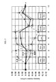
Here, A is the x-direction aberration coefficient, B is the y-direction aberration coefficient, D is the energy dispersion coefficient, AA, BB, AB are respectively secondary aberration coefficients relating to the open angle of the beam spaces. When the above parameters with the values in the boxes at the lower part of FIG. 5 are established as the specific embodiment of the present invention, the changes in the primary aberration coefficients and secondary aberration coefficients are shown in FIG. 6 and FIG. 7 . The horizontal axis indicates the progression direction of the z axis. The left end (0) in the figure is the theoretical object point for the beam input side, and the right end (10) is the ghost image point on the beam output side. In other words, the right end (10) is the monochrome convergence point.
As clearly shown in FIG. 6 , with the aberration coefficient A for the x-direction open angle α, and the aberration coefficient B for the y-direction open angle β simultaneously converging (A=B=0), the energy dispersion coefficient D reaches −0.04. The x-direction and y-direction simultaneously converge on the monochrome convergence point at the right end (10), moreover the dispersion is canceled out. In this way, in the primary formula for the trajectory calculation, the monochromator of the present invention is triple-converged (A=B=D=0) both in terms of space and energy.
In the secondary aberration coefficient of FIG. 7 , the three secondary aberration coefficients have been eliminated at the right end monochrome convergence point (AA=BB=AB=0). This is the effect of mirror symmetry at the monochromator slit position, and perpendicular input of the beam to the plane of the sectorial magnetic field.
As described above, if the monochromator of the present invention is installed below the first focus lens of the scanning electron microscope, all of the monochrome convergence points converged using the primary and secondary aberration coefficients A, B, D, AA, BB, AB can be obtained after limiting the beam energy at the slits. These are set as object point for the second focus lens, and by contracting (the focus point) with the objective lens, an extremely small spot with few chromatic aberrations can be obtained and the resolution of the scanning electron microscope improved.
The method for adjusting the monochromator of the present invention is described next while referring to FIG. 8 .
(A) First of all, the drive (excitation) of magnetic field generator 21 on the monochromator 20 is cut off and an actual image of the electron source is formed on the mirror symmetric surface 18. A beam restrictor 14 with a diameter of approximately 500 micrometers is installed for that purpose. By then using the adjustment scanning coil 4 a to perform two-dimensional scanning with electron beam 3 s with this beam restrictor 14, a condensed SEM image can be acquired, and an actual image obtained under optimal image resolution conditions. Adjusting the second focus lens and objective lens with these conditions allows optimizing the SEM image resolution of the sample.
(B) Next, as the drive (excitation) of the magnetic field generator 21 is successively amplified, an electron beam 3 t is irradiated onto the electrode of a first electrical field generator 22 only when the drive or excitation is within a certain range. By setting the excitation current of magnetic field generator 21 to an intermediate value for the current flowing into the external electrode, it is possible to make adjustments based on accurate, optimal excitation conditions.
(C) The electron beam 3 u is irradiated onto the electrode of a second electrical field generator 23 when the voltage of the first electrical field generator 22 is increased. By measuring the electrical current flow into the external electrode, it is possible to find the conditions needed for applying a voltage for irradiating the center of the gap of the second electrical field generator 23 with an electron beam. This enables to make adjustments based on accurate voltage application conditions the same as when adjusting the sectorial magnetic field.
(D) Set the second electrical field generator 23 to the same voltage conditions as the first electrical field generator 22.
(E) Compare with the SEM image of the sample in (A), and make fine adjustments to the voltage of the first electrical field generator 22 and second electrical field generator 23 to minimize defocusing or image shifting.
(F) Insert a beam restrictor 24 up to the crossover 19 of the electron beam. Make fine adjustments using the scanning coil 4 a so that beam restrictor 24 is in the center of the image.
The reference numerals 3, 3 d and 3 e in FIG. 9 represent results calculated for beam shape using TRIO under the conditions for focusing the electron beam at the beam restrictor 24 position. A beam shape with a wide energy width is a dispersion image such as represented by 3 f. Although the constriction in beam width in the y direction is small relative to a hole of approximately 4 micrometers, a widening effect occurs in the x-direction due to the diffusion of energy, making it impossible to observe clear and sharp focused image. There is, however, little change in energy dispersion due to focus adjustment so fine adjustments may be made to the sectorial toroidal electrical field under the condition that the lateral width of the entire image is minimum. Finally, check that the monochrome point on the mirror symmetric surface 18 matches the actual image formed prior to excitation by the sectorial magnetic field of the magnetic field generator 21 as seen from the output slit of monochromator 20. This method makes the optical conditions downstream of the monochromator completely identical, and fine adjustments made to the second electrical field generator 23 parameters prevent image shifts and defocusing from occurring before or after excitation of the magnetic field generator 21.
A specific method for adjusting the parameters of the sectorial toroidal electrical field is described while referring to FIG. 10 . By making the electrical field into a toroidal electrical field, a convergence effect is generated in the y-direction. Two adjustment terminals 22 c and 22 d are installed in the y-direction for making fine adjustments to the toroidal electrical field. Applying the same voltage Vc to these electrodes makes tiny changes in the toroidal constant, for changing the y-direction convergence point. The focus point can also be adjusted in the y-direction, not only in the x-direction.
The electrodes 22 a, 22 b that comprise the sectorial toroidal electrical field of the present embodiment have a curvature along the electron beam trajectory. These electrodes 22 a, 22 b further have a shape with a particular curvature radius Ry along the y-direction of their cross section. Electrodes shaped in this way can generate a convergence effect in the y-direction.
These electrodes 22 a, 22 b and the adjusting electrodes 22 c, 22 d are respectively connected to a variable power supply (not shown in drawing).
The second embodiment of the invention is described next. The energy dispersion trajectory 3 d is shown in FIG. 11 . The energy dispersion trajectory is emitted at the point in time that the first sectorial magnetic field formed by the magnetic field generator 21 is irradiated. This becomes uniform after passing the first sectorial electrical field formed by the first electrical field generator 22 and passes through the beam restrictor 24. After then passing along the mirror-symmetrical trajectory, the energy dispersion diminishes and becomes completely zero at the point of emission from the sectorial magnetic field formed by the magnetic field generator 21. Even after emission, the energy dispersion of the electron beam 3 d remains unchanged at zero. Summing the above, since the energy dispersion along the linear optical axis is always zero, the beam is subjected to point convergence and triple convergence from energy non-dispersion regardless of the point convergence position. The optical parameters for this kind of completely monochrome conditions are summarized in the lower half of FIG. 11 . In a monochromator configured with these values, even if the convergent point position has shifted from a change in the parameters due to other optical elements on the optical axis, stable monochrome conditions can always be restored and, thus, it is easy to adjust the device.
The changes in the aberration coefficients when the above parameters were set are shown in FIG. 12 and FIG. 13 . As FIG. 12 clearly shows, while the aberration coefficient A for the x direction open angle α of and the aberration coefficient B for the y direction of open angle β are simultaneously converged (A=B=0) on the beam restrictor 24 position (5), the energy dispersion coefficient D is reaching −0.04 the same as in the previous embodiment. Simultaneous convergence is taking place in the x direction and y direction at the monochrome convergence point on the right end (10). Furthermore, the dispersion is canceled out immediately after emission from the fan shaped magnetic field. The monochromator of the present invention is in this way triple-converged (A=B=D=0) in the primary formula for the trajectory calculation, both in terms of space and energy. It should be noted in particular that D is always at zero from the emission point (9) of the sectorial magnetic field onwards. Further, in the secondary aberration coefficient changes as shown in FIG. 13 , the three aberration coefficients are all eliminated (AA=BB=0) at the monochrome point on the right end (10). This is the effect of mirror symmetry at the monochromator slit position (5), and the perpendicular input of the beam perpendicular to the plane of the sectorial magnetic field.
The embodiments of the present invention allow high resolution in a low acceleration SEM where it was previously impossible to obtain a resolution within 2 nanometers. Though Schottky emission electron sources and thermal field emission electron sources offered superior characteristics in terms of continuous stable operation over several thousand hours, these devices had the problem that energy width was relatively large at approximately 0.6 eV and also large problems with chromatic aberrations compared to cooled-cathode discharge electron sources. However, both long term stable operation and reduced chromatic aberrations can be achieved by utilizing the monochromator described in the present embodiments.
The example in the embodiments of the present invention described a scanning electron microscope (SEM) using a monochromator at a low acceleration voltage. However, the present invention may also be applied to scanning transmission type electron microscopes (STEM) and high acceleration scanning electron microscopes.
As described above, by installing the monochromator of the embodiment of the present invention in a scanning electron microscope, a monochromatized convergence or focus point can be obtained for all primary and secondary energy with slits. By setting this point as the object point for the focus lens and reducing it with the objective lens, an extremely tiny spot with few chromatic aberrations can be obtained and the resolution of the SEM improved.
There is also absolutely no need to change optical conditions other than for the monochromator either before or after monochromator operation so that high reliability along with simple maintenance is achieved making the invention particularly effective for use on semiconductor device production lines.
The invention as described above, renders the effect of achieving high image resolution while suppressing the generation of higher-order aberrations without lowering the beam focusing effect.
Claims (7)
1. A scanning transmission type electron microscope having an objective lens that focuses an electron beam emitted from an electron source on a sample, comprising:
a monochromator installed between the electron source and the objective lens,
wherein the monochromator deflects an electron beam using a magnetic field generator and deflects the electron beam using a first electrical field generator to disperse the energy of the electron beam, and
wherein the monochromator further deflects an electron beam that has passed through a slit using a second electrical field generator so that the electron beam returns to the magnetic field generator.
2. The scanning transmission type electron microscope according to claim 1 ,
wherein the electron beam is deflected by a magnetic field generated by the magnetic field generator, and
wherein the electron beam that has passed through the magnetic field is deflected by an electrical field generated by the first electrical field generator so that the energy of the electron beam is dispersed.
3. The scanning transmission type electron microscope according to claim 1 ,
wherein the monochromator comprises a prestage deflection system including the magnetic field generator and the first electrical field generator, a final deflection system including the second electrical field generator and the magnetic field generator, the final deflection system being installed in a mirror-symmetrical position with respect to the prestage deflection system, and the slit installed on a mirror-symmetrical surface between the prestage and final deflection systems, and
wherein the final deflection system cancels out the energy dispersion of the electron beam generated by the prestage deflection system.
4. The scanning transmission type electron microscope according to claim 1 ,
wherein the monochromator is installed between first and second focus lenses for focusing an electron beam, and
wherein excitation conditions of the first and second focus lenses do not change before or after the alternation of an excitation of the magnetic field generator included in the monochromator.
5. The scanning transmission type electron microscope according to claim 1 , wherein an electrode included in each of the first and second electrical field generators forms a fan shape.
6. The scanning transmission type electron microscope according to claim 1 , wherein a magnetic pole included in the magnetic field generator has input and output beam surfaces perpendicular to the electron beam.
7. The scanning transmission type electron microscope according to claim 1 ,
wherein the monochromator comprises a prestage deflection system including the magnetic field generator and the first electrical field generator, a final deflection system including the second electrical field generator and the magnetic field generator, the final deflection system being installed in a mirror-symmetrical position with respect to the prestage deflection system, and the slit installed on a mirror-symmetrical surface between the prestage and final deflection systems,
wherein the prestage deflection system spatially converges the electron beam at the position of the slit and limits the energy width of the electron beam with the slit, and
wherein the final deflection system spatially converges the electron beam again and reduces the energy dispersion of the electron beam.
Priority Applications (1)
| Application Number | Priority Date | Filing Date | Title |
|---|---|---|---|
| US11/987,018 US7838827B2 (en) | 2003-01-08 | 2007-11-26 | Monochromator and scanning electron microscope using the same |
Applications Claiming Priority (5)
| Application Number | Priority Date | Filing Date | Title |
|---|---|---|---|
| JP2003001686A JP3867048B2 (en) | 2003-01-08 | 2003-01-08 | Monochromator and scanning electron microscope using the same |
| JP2003-001686 | 2003-01-08 | ||
| US10/751,907 US7022983B2 (en) | 2003-01-08 | 2004-01-07 | Monochromator and scanning electron microscope using the same |
| US11/344,529 US7315024B2 (en) | 2003-01-08 | 2006-02-01 | Monochromator and scanning electron microscope using the same |
| US11/987,018 US7838827B2 (en) | 2003-01-08 | 2007-11-26 | Monochromator and scanning electron microscope using the same |
Related Parent Applications (1)
| Application Number | Title | Priority Date | Filing Date |
|---|---|---|---|
| US11/344,529 Continuation US7315024B2 (en) | 2003-01-08 | 2006-02-01 | Monochromator and scanning electron microscope using the same |
Publications (2)
| Publication Number | Publication Date |
|---|---|
| US20080237463A1 US20080237463A1 (en) | 2008-10-02 |
| US7838827B2 true US7838827B2 (en) | 2010-11-23 |
Family
ID=32819644
Family Applications (3)
| Application Number | Title | Priority Date | Filing Date |
|---|---|---|---|
| US10/751,907 Expired - Fee Related US7022983B2 (en) | 2003-01-08 | 2004-01-07 | Monochromator and scanning electron microscope using the same |
| US11/344,529 Expired - Fee Related US7315024B2 (en) | 2003-01-08 | 2006-02-01 | Monochromator and scanning electron microscope using the same |
| US11/987,018 Expired - Fee Related US7838827B2 (en) | 2003-01-08 | 2007-11-26 | Monochromator and scanning electron microscope using the same |
Family Applications Before (2)
| Application Number | Title | Priority Date | Filing Date |
|---|---|---|---|
| US10/751,907 Expired - Fee Related US7022983B2 (en) | 2003-01-08 | 2004-01-07 | Monochromator and scanning electron microscope using the same |
| US11/344,529 Expired - Fee Related US7315024B2 (en) | 2003-01-08 | 2006-02-01 | Monochromator and scanning electron microscope using the same |
Country Status (3)
| Country | Link |
|---|---|
| US (3) | US7022983B2 (en) |
| JP (1) | JP3867048B2 (en) |
| NL (1) | NL1025182C2 (en) |
Cited By (3)
| Publication number | Priority date | Publication date | Assignee | Title |
|---|---|---|---|---|
| US20100044565A1 (en) * | 2006-01-05 | 2010-02-25 | Hitachi High-Technologies Corporation | Scanning electron microscope having a monochromator |
| US8334508B1 (en) * | 2011-02-22 | 2012-12-18 | Electron Optica, Inc. | Mirror energy filter for electron beam apparatus |
| US9443696B2 (en) | 2014-05-25 | 2016-09-13 | Kla-Tencor Corporation | Electron beam imaging with dual Wien-filter monochromator |
Families Citing this family (12)
| Publication number | Priority date | Publication date | Assignee | Title |
|---|---|---|---|---|
| JP4074185B2 (en) * | 2002-12-17 | 2008-04-09 | 日本電子株式会社 | Energy filter and electron microscope |
| JP3867048B2 (en) * | 2003-01-08 | 2007-01-10 | 株式会社日立ハイテクノロジーズ | Monochromator and scanning electron microscope using the same |
| EP1883094B1 (en) * | 2006-07-24 | 2012-05-02 | ICT, Integrated Circuit Testing Gesellschaft für Halbleiterprüftechnik mbH | Charged particle beam device and method for inspecting specimen |
| JP4896626B2 (en) | 2006-08-22 | 2012-03-14 | 株式会社日立ハイテクノロジーズ | Scanning electron microscope |
| DE102007024353B4 (en) * | 2007-05-24 | 2009-04-16 | Ceos Corrected Electron Optical Systems Gmbh | Monochromator and beam source with monochromator |
| EP2385542B1 (en) * | 2010-05-07 | 2013-01-02 | ICT Integrated Circuit Testing Gesellschaft für Halbleiterprüftechnik mbH | Electron beam device with dispersion compensation, and method of operating same |
| JP6254445B2 (en) * | 2014-01-09 | 2017-12-27 | 株式会社日立ハイテクノロジーズ | Charged particle beam equipment |
| WO2016055319A1 (en) | 2014-10-06 | 2016-04-14 | Koninklijke Philips N.V. | Modification arrangement for an x-ray generating device |
| US10283315B2 (en) | 2017-05-16 | 2019-05-07 | International Business Machines Corporation | Measuring spherical and chromatic aberrations in cathode lens electrode microscopes |
| US10964522B2 (en) | 2018-06-06 | 2021-03-30 | Kla Corporation | High resolution electron energy analyzer |
| JP2019215957A (en) * | 2018-06-11 | 2019-12-19 | 株式会社荏原製作所 | Beam bender |
| US20230215682A1 (en) * | 2021-12-30 | 2023-07-06 | Fei Company | Electrostatic mirror chromatic aberration correctors |
Citations (23)
| Publication number | Priority date | Publication date | Assignee | Title |
|---|---|---|---|---|
| JPS59143252A (en) | 1983-02-03 | 1984-08-16 | Jeol Ltd | Electric field generating apparatus |
| US5126565A (en) * | 1990-08-08 | 1992-06-30 | U.S. Philips Corp. | Energy filter for charged particle beam apparatus |
| JPH0737536A (en) | 1993-03-26 | 1995-02-07 | Carl Zeiss:Fa | Electronic energy filter for image formation |
| DE19633496A1 (en) | 1996-08-20 | 1998-02-26 | Ceos Corrected Electron Option | Monochromator for electron microscopy |
| US5811801A (en) * | 1995-11-28 | 1998-09-22 | Jeol Ltd. | Omega-type energy filter |
| JPH11191384A (en) | 1997-10-20 | 1999-07-13 | Jeol Ltd | Transmission type electron microscope equipped with energy filter |
| JPH11195396A (en) | 1997-10-23 | 1999-07-21 | Leo Elektronenmikroskopie Gmbh | Corpuscular beam device having energy filter |
| US6015973A (en) * | 1996-10-16 | 2000-01-18 | Jeol Ltd. | Energy Filter |
| US6040567A (en) | 1997-03-14 | 2000-03-21 | Max-Planck-Gesellschaft Zur Forderung Der Wissenschaften E.V. | Method and device for controlling fast periodic motion |
| US6097028A (en) * | 1997-02-27 | 2000-08-01 | Jeol Ltd. | Energy filter |
| US6140645A (en) | 1997-10-20 | 2000-10-31 | Jeol Ltd. | Transmission electron microscope having energy filter |
| US6150657A (en) * | 1997-08-28 | 2000-11-21 | Hitachi, Ltd. | Energy filter and electron microscope equipped with the energy filter |
| DE10020382A1 (en) | 2000-04-26 | 2001-10-31 | Ceos Gmbh | Beam generation system for electrons or ion beams of high monochrome or high current density |
| JP2001357809A (en) | 2000-04-10 | 2001-12-26 | Jeol Ltd | Monochromator for electron beam |
| US20020017614A1 (en) * | 2000-07-06 | 2002-02-14 | Michiyoshi Tanaka | Energy filter |
| US20020033455A1 (en) * | 2000-02-08 | 2002-03-21 | Harald Rose | Electron energy filter with magnetic deflecting regions |
| US6495826B2 (en) | 2000-04-10 | 2002-12-17 | Jeol, Ltd. | Monochrometer for electron beam |
| JP2003132828A (en) | 2001-10-26 | 2003-05-09 | Hitachi High-Technologies Corp | Scanning electron microscope with monochromator |
| US20040188607A1 (en) * | 2003-01-08 | 2004-09-30 | Yoichi Ose | Monochromator and scanning electron microscope using the same |
| US7006235B2 (en) * | 2000-09-20 | 2006-02-28 | Kla-Tencor Technologies Corp. | Methods and systems for determining overlay and flatness of a specimen |
| US20070138403A1 (en) | 2003-08-28 | 2007-06-21 | Dane Cubric | Particle optical apparatus |
| US20070181805A1 (en) * | 2006-01-05 | 2007-08-09 | Wataru Mori | Scanning electron microscope having a monochromator |
| JP4233145B2 (en) | 1997-05-02 | 2009-03-04 | アルカテル−ルーセント | Method and apparatus for manufacturing glass fiber preform |
Family Cites Families (1)
| Publication number | Priority date | Publication date | Assignee | Title |
|---|---|---|---|---|
| JP3423675B2 (en) | 2000-07-13 | 2003-07-07 | 住友重機械工業株式会社 | Charged particle beam irradiation device and treatment device using the same |
-
2003
- 2003-01-08 JP JP2003001686A patent/JP3867048B2/en not_active Expired - Fee Related
-
2004
- 2004-01-07 NL NL1025182A patent/NL1025182C2/en not_active IP Right Cessation
- 2004-01-07 US US10/751,907 patent/US7022983B2/en not_active Expired - Fee Related
-
2006
- 2006-02-01 US US11/344,529 patent/US7315024B2/en not_active Expired - Fee Related
-
2007
- 2007-11-26 US US11/987,018 patent/US7838827B2/en not_active Expired - Fee Related
Patent Citations (32)
| Publication number | Priority date | Publication date | Assignee | Title |
|---|---|---|---|---|
| JPS59143252A (en) | 1983-02-03 | 1984-08-16 | Jeol Ltd | Electric field generating apparatus |
| US5126565A (en) * | 1990-08-08 | 1992-06-30 | U.S. Philips Corp. | Energy filter for charged particle beam apparatus |
| JPH04233145A (en) | 1990-08-08 | 1992-08-21 | Philips Gloeilampenfab:Nv | Energy filter |
| JPH0737536A (en) | 1993-03-26 | 1995-02-07 | Carl Zeiss:Fa | Electronic energy filter for image formation |
| US5449914A (en) * | 1993-03-26 | 1995-09-12 | Carl-Zeiss-Stiftung | Imaging electron energy filter |
| US5811801A (en) * | 1995-11-28 | 1998-09-22 | Jeol Ltd. | Omega-type energy filter |
| DE19633496A1 (en) | 1996-08-20 | 1998-02-26 | Ceos Corrected Electron Option | Monochromator for electron microscopy |
| US6015973A (en) * | 1996-10-16 | 2000-01-18 | Jeol Ltd. | Energy Filter |
| US6097028A (en) * | 1997-02-27 | 2000-08-01 | Jeol Ltd. | Energy filter |
| US6040567A (en) | 1997-03-14 | 2000-03-21 | Max-Planck-Gesellschaft Zur Forderung Der Wissenschaften E.V. | Method and device for controlling fast periodic motion |
| JP4233145B2 (en) | 1997-05-02 | 2009-03-04 | アルカテル−ルーセント | Method and apparatus for manufacturing glass fiber preform |
| US6150657A (en) * | 1997-08-28 | 2000-11-21 | Hitachi, Ltd. | Energy filter and electron microscope equipped with the energy filter |
| US6140645A (en) | 1997-10-20 | 2000-10-31 | Jeol Ltd. | Transmission electron microscope having energy filter |
| JPH11191384A (en) | 1997-10-20 | 1999-07-13 | Jeol Ltd | Transmission type electron microscope equipped with energy filter |
| US6239430B1 (en) | 1997-10-23 | 2001-05-29 | Leo Elektronenmikroskopie Gmbh | Particle beam apparatus with energy filter |
| JPH11195396A (en) | 1997-10-23 | 1999-07-21 | Leo Elektronenmikroskopie Gmbh | Corpuscular beam device having energy filter |
| US20020033455A1 (en) * | 2000-02-08 | 2002-03-21 | Harald Rose | Electron energy filter with magnetic deflecting regions |
| JP2001357809A (en) | 2000-04-10 | 2001-12-26 | Jeol Ltd | Monochromator for electron beam |
| US6495826B2 (en) | 2000-04-10 | 2002-12-17 | Jeol, Ltd. | Monochrometer for electron beam |
| DE10020382A1 (en) | 2000-04-26 | 2001-10-31 | Ceos Gmbh | Beam generation system for electrons or ion beams of high monochrome or high current density |
| US20030098414A1 (en) * | 2000-04-26 | 2003-05-29 | Stephan Uhlemann | Electron/ion gun for electron or ion beams with high monochromasy or high current density |
| US6770878B2 (en) * | 2000-04-26 | 2004-08-03 | Ceos Corrected Electron Optical Systems Gmbh | Electron/ion gun for electron or ion beams with high monochromasy or high current density |
| US6624412B2 (en) * | 2000-07-06 | 2003-09-23 | Jeol Ltd. | Energy filter |
| US20020017614A1 (en) * | 2000-07-06 | 2002-02-14 | Michiyoshi Tanaka | Energy filter |
| US7006235B2 (en) * | 2000-09-20 | 2006-02-28 | Kla-Tencor Technologies Corp. | Methods and systems for determining overlay and flatness of a specimen |
| JP2003132828A (en) | 2001-10-26 | 2003-05-09 | Hitachi High-Technologies Corp | Scanning electron microscope with monochromator |
| US20040188607A1 (en) * | 2003-01-08 | 2004-09-30 | Yoichi Ose | Monochromator and scanning electron microscope using the same |
| US20060219910A1 (en) * | 2003-01-08 | 2006-10-05 | Yoichi Ose | Monochromator and scanning electron microscope using the same |
| US7315024B2 (en) * | 2003-01-08 | 2008-01-01 | Hitachi High-Technologies Corporation | Monochromator and scanning electron microscope using the same |
| US7022983B2 (en) * | 2003-01-08 | 2006-04-04 | Hitachi High-Technologies Corporation | Monochromator and scanning electron microscope using the same |
| US20070138403A1 (en) | 2003-08-28 | 2007-06-21 | Dane Cubric | Particle optical apparatus |
| US20070181805A1 (en) * | 2006-01-05 | 2007-08-09 | Wataru Mori | Scanning electron microscope having a monochromator |
Cited By (4)
| Publication number | Priority date | Publication date | Assignee | Title |
|---|---|---|---|---|
| US20100044565A1 (en) * | 2006-01-05 | 2010-02-25 | Hitachi High-Technologies Corporation | Scanning electron microscope having a monochromator |
| US8067733B2 (en) * | 2006-01-05 | 2011-11-29 | Hitachi High-Technologies Corporation | Scanning electron microscope having a monochromator |
| US8334508B1 (en) * | 2011-02-22 | 2012-12-18 | Electron Optica, Inc. | Mirror energy filter for electron beam apparatus |
| US9443696B2 (en) | 2014-05-25 | 2016-09-13 | Kla-Tencor Corporation | Electron beam imaging with dual Wien-filter monochromator |
Also Published As
| Publication number | Publication date |
|---|---|
| US20040188607A1 (en) | 2004-09-30 |
| US20080237463A1 (en) | 2008-10-02 |
| NL1025182C2 (en) | 2006-03-06 |
| US7022983B2 (en) | 2006-04-04 |
| JP3867048B2 (en) | 2007-01-10 |
| US20060219910A1 (en) | 2006-10-05 |
| JP2004214111A (en) | 2004-07-29 |
| US7315024B2 (en) | 2008-01-01 |
| NL1025182A1 (en) | 2004-07-09 |
Similar Documents
| Publication | Publication Date | Title |
|---|---|---|
| US7838827B2 (en) | Monochromator and scanning electron microscope using the same | |
| USRE49784E1 (en) | Apparatus of plural charged-particle beams | |
| US20240128044A1 (en) | Apparatus of plural charged-particle beams | |
| EP1381073B1 (en) | Aberration-corrected charged-particle optical apparatus | |
| EP2575144B1 (en) | Particle-optical systems and arrangements and particle-optical components for such systems and arrangements | |
| CN109216143A (en) | Charged particle beam apparatus and the method part that sample is imaged or is illuminated | |
| EP2405460B1 (en) | Electron beam device with tilting and dispersion compensation, and method of operating same | |
| TWI788801B (en) | Particle beam system having a multi-pole lens sequence for independently focussing a multiplicity of individual particle beams, its use and associated method | |
| US20180005797A1 (en) | Scanning electron microscope | |
| US6878937B1 (en) | Prism array for electron beam inspection and defect review | |
| US7105833B2 (en) | Deflection system for a particle beam device | |
| JP4781211B2 (en) | Electron beam apparatus and pattern evaluation method using the same | |
| US11239042B2 (en) | Beam irradiation device | |
| US7679054B2 (en) | Double stage charged particle beam energy width reduction system for charged particle beam system | |
| US6608308B1 (en) | Electrostatic lens systems for secondary-electron mapping-projection apparatus, and mapping-projection apparatus and methods comprising same | |
| US20220336186A1 (en) | Charged particle beam apparatus, multi-beamlet assembly, and method of inspecting a specimen | |
| US8373137B2 (en) | High resolution energy-selecting electron beam apparatus | |
| JP2007035386A (en) | Electron beam apparatus and device manufacturing method using same | |
| RU2144237C1 (en) | Optical particle-emitting column | |
| WO2021220388A1 (en) | Charged particle beam device | |
| CN116745880A (en) | Electron optical column and method for directing primary electron beam onto sample | |
| KR20230123969A (en) | Electron optical column and method for directing a primary electron beam to a sample |
Legal Events
| Date | Code | Title | Description |
|---|---|---|---|
| FEPP | Fee payment procedure |
Free format text: PAYOR NUMBER ASSIGNED (ORIGINAL EVENT CODE: ASPN); ENTITY STATUS OF PATENT OWNER: LARGE ENTITY |
|
| FPAY | Fee payment |
Year of fee payment: 4 |
|
| FEPP | Fee payment procedure |
Free format text: MAINTENANCE FEE REMINDER MAILED (ORIGINAL EVENT CODE: REM.) |
|
| LAPS | Lapse for failure to pay maintenance fees |
Free format text: PATENT EXPIRED FOR FAILURE TO PAY MAINTENANCE FEES (ORIGINAL EVENT CODE: EXP.); ENTITY STATUS OF PATENT OWNER: LARGE ENTITY |
|
| STCH | Information on status: patent discontinuation |
Free format text: PATENT EXPIRED DUE TO NONPAYMENT OF MAINTENANCE FEES UNDER 37 CFR 1.362 |
|
| FP | Lapsed due to failure to pay maintenance fee |
Effective date: 20181123 |