US7831778B2 - Shared nonvolatile memory architecture - Google Patents
Shared nonvolatile memory architecture Download PDFInfo
- Publication number
- US7831778B2 US7831778B2 US11/690,629 US69062907A US7831778B2 US 7831778 B2 US7831778 B2 US 7831778B2 US 69062907 A US69062907 A US 69062907A US 7831778 B2 US7831778 B2 US 7831778B2
- Authority
- US
- United States
- Prior art keywords
- processing component
- memory
- component
- initialization
- processing
- Prior art date
- Legal status (The legal status is an assumption and is not a legal conclusion. Google has not performed a legal analysis and makes no representation as to the accuracy of the status listed.)
- Active, expires
Links
Images


Classifications
-
- G—PHYSICS
- G06—COMPUTING; CALCULATING OR COUNTING
- G06F—ELECTRIC DIGITAL DATA PROCESSING
- G06F12/00—Accessing, addressing or allocating within memory systems or architectures
-
- G—PHYSICS
- G06—COMPUTING; CALCULATING OR COUNTING
- G06F—ELECTRIC DIGITAL DATA PROCESSING
- G06F15/00—Digital computers in general; Data processing equipment in general
- G06F15/16—Combinations of two or more digital computers each having at least an arithmetic unit, a program unit and a register, e.g. for a simultaneous processing of several programs
- G06F15/177—Initialisation or configuration control
-
- G—PHYSICS
- G06—COMPUTING; CALCULATING OR COUNTING
- G06F—ELECTRIC DIGITAL DATA PROCESSING
- G06F13/00—Interconnection of, or transfer of information or other signals between, memories, input/output devices or central processing units
- G06F13/14—Handling requests for interconnection or transfer
- G06F13/16—Handling requests for interconnection or transfer for access to memory bus
-
- G—PHYSICS
- G06—COMPUTING; CALCULATING OR COUNTING
- G06F—ELECTRIC DIGITAL DATA PROCESSING
- G06F8/00—Arrangements for software engineering
- G06F8/40—Transformation of program code
- G06F8/54—Link editing before load time
-
- G—PHYSICS
- G06—COMPUTING; CALCULATING OR COUNTING
- G06F—ELECTRIC DIGITAL DATA PROCESSING
- G06F9/00—Arrangements for program control, e.g. control units
- G06F9/06—Arrangements for program control, e.g. control units using stored programs, i.e. using an internal store of processing equipment to receive or retain programs
- G06F9/44—Arrangements for executing specific programs
- G06F9/4401—Bootstrapping
- G06F9/4405—Initialisation of multiprocessor systems
-
- G—PHYSICS
- G06—COMPUTING; CALCULATING OR COUNTING
- G06F—ELECTRIC DIGITAL DATA PROCESSING
- G06F9/00—Arrangements for program control, e.g. control units
- G06F9/06—Arrangements for program control, e.g. control units using stored programs, i.e. using an internal store of processing equipment to receive or retain programs
- G06F9/46—Multiprogramming arrangements
Definitions
- Mobile devices with multiple processing components dedicated to separate tasks are becoming increasingly common.
- mobile phones often contain a baseband processor dedicated to handling the connection and disconnection of calls, and a separate media processor dedicated to displaying a user interface and receiving requests from a user.
- Such components may share a volatile main memory for use during operation, or each component may have a dedicated memory.
- Each component may have its own nonvolatile memory used to store startup logic and configuration data.
- each component may have its own proprietary interface for communication with the other components.
- the cost of manufacturing a device is directly related to the number of components included within the device. Therefore, it is a common manufacturing goal to reduce or eliminate redundant components to save money. Additional components also increase the power consumption of the device, which directly affects the battery life of mobile devices. Therefore, reducing components also prolongs battery life. In addition, the number of buses and other interfaces between components increases the complexity of a device. Increased complexity contributes to the difficulty of designing and testing the device and increases the time required to bring a new product to market.
- Flash memory is available in two types, NAND and NOR, referring to the predominant type of logic gates used within the flash memory for storing data.
- NAND flash memory is fast, having microsecond access times, while NAND flash memory is slower, typically having millisecond access times.
- this speed comes with a price, and NOR flash memory is more expensive than NAND flash memory.
- Device manufacturers must make a trade-off between the speed of the flash memory and its cost.
- FIG. 1 is a block diagram that illustrates components of a shared memory system.
- FIG. 2 is a flow diagram that illustrates the processing of a device containing the shared memory during initialization.
- FIG. 3 is a memory diagram that illustrates the contents of a flash memory and a random access memory in the device during initialization.
- FIG. 4 is a flow diagram that illustrates the validation of initialization logic during initialization.
- a method and system that utilizes a shared nonvolatile memory for initializing multiple processing components is provided, referred to as a shared memory system.
- the shared memory system reduces the number of nonvolatile memory components used to initialize multiple processing components within a device.
- the startup logic and configuration data for processing components within a device is stored in a single nonvolatile memory.
- the shared memory system copies the startup logic and configuration data from the nonvolatile memory to the volatile main memory. Then, each processing component accesses the main memory to find its startup logic and configuration data and begin executing.
- Main memory is typically much faster than flash memory.
- the movement of the startup logic from the nonvolatile memory to main memory reduces the importance of the speed of the nonvolatile memory, since it is only a factor during the initial copying.
- the shared memory system allows a device manufacturer to select a cheaper nonvolatile memory component without a significant impact on the startup speed of the device.
- the device manufacturer already has to design each component to access main memory during normal operation, it is not necessary to design an additional interface for accessing the nonvolatile memory when the startup logic is available from main memory. In this way, the shared memory system simplifies the design of each component, leading to less complexity and lower power consumption.
- the shared memory system utilizes a serial-port memory component, such as the MemoryLink architecture described in U.S. patent application Ser. No. 10/045,297, entitled “COMMUNICATIONS ARCHITECTURE FOR MEMORY-BASED DEVICES”, and filed on Nov. 7, 2001, which is incorporated herein by reference.
- the above-referenced application describes a serial-port memory that allows multiple devices, such as the processing components described above, to access a single main memory device.
- the architecture includes mechanisms for accessing the memory, and for communicating events between devices to indicate the completion of operations.
- the processing components may have a separate interface connecting them that the processing components use to synchronize their activities.
- the shared memory system designates one of the processing components to be a master processing component.
- the master processing component is the only processing component attached to the non-volatile (e.g., flash) memory component.
- the master processing component is responsible for copying the contents of the non-volatile memory component to the main memory component.
- the master processing component signals the other processing components to begin their startup sequence, such as by using the signaling mechanisms described above.
- the master processing component also begins its startup sequence by accessing the main memory component, which contains the copied contents of the non-volatile memory component. In this way, only one processing component is designed with a separate interface to the non-volatile memory component, yet the contents of the non-volatile memory component are made available to each of the processing components.
- FIG. 1 is a block diagram that illustrates components of the shared memory system, in some embodiments.
- a device 100 using the shared memory system comprises a flash memory component 110 or other nonvolatile memory component, a first processing component 120 , at least one other processing component 130 , and a main random access memory (RAM) 140 or other volatile memory component.
- the flash memory component 110 contains startup logic and configuration data that is stored for each of the processing components during periods when the power has been removed from the shared memory system.
- the first processing component 120 is configured as a master processing component and is attached to the flash memory component 110 . During startup of the device 100 , the first processing component 120 copies the contents of the flash memory component 110 to the random access memory 140 .
- Each of the processing components 120 and 130 is connected to the random access memory 140 .
- each of the processing components 120 and 130 begin their startup sequence by accessing startup logic and configuration data directly from the random access memory 140 . While only two processing components are depicted in FIG. 1 , it will be appreciated that any number of processing or other components may be coupled to the shared memory system.
- the processors may also differ from each other and perform different functions. For example, in mobile applications one processor may be a baseband processor and another processor may be an application processor.
- the device on which the system is implemented may include a central processing unit, memory, input devices (e.g., keyboard and pointing devices), output devices (e.g., visual displays, audio speakers), and storage devices (e.g., disk drives).
- the memory and storage devices are computer-readable media that may be encoded with computer-executable instructions that implement the disclosed technology, which means a computer-readable medium that contains appropriate instructions.
- the data structures and message structures may be stored or transmitted via a data transmission medium, such as a signal on a communication link.
- Various communication links may be used, such as the Internet, a local area network, a wide area network, a point-to-point dial-up connection, a cell phone network, and so on.
- Embodiments of the system may be implemented in various mobile operating environments that include personal computers, server computers, handheld or laptop devices, multiprocessor systems, microprocessor-based systems, programmable consumer electronics, digital cameras, network PCs, minicomputers, distributed computing environments that include any of the above systems or devices, and so on.
- the computer systems may be cell phones, personal digital assistants, smart phones, personal computers, programmable consumer electronics, digital cameras, and so on.
- program modules include hardware logic, routines, programs, objects, components, data structures, and so on that perform particular tasks or implement particular abstract data types.
- functionality of the program modules may be combined or distributed as desired in various embodiments.
- FIG. 2 is a flow diagram that illustrates the processing of the device during initialization, in one embodiment.
- Initialization occurs when power is first applied to the device or when the device performs a hard reset.
- the device starts the master processor.
- the device instructs the master processor to begin executing instructions from the flash memory component (or other non-volatile memory component) that instruct the master processor to copy the contents of the flash memory to the random access memory (or other volatile memory).
- the device signals each of the processors to begin initialization using the random access memory component.
- the first processor locates its initialization instructions within the random access memory and begins executing the initialization instructions.
- the other processors locate their respective initialization instructions within the random access memory and begin executing the initialization instructions. After step 250 the device is initialized and these steps conclude.
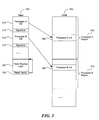
- FIG. 3 is a memory diagram that illustrates the contents of the flash memory and the random access memory during initialization, in one embodiment.
- the diagram contains a flash memory 305 and a random access memory 350 .
- the flash memory 305 contains initialization logic 310 for a first processing component, initialization logic 315 for another processing component, flash shadow logic 320 , and a boot reset vector 325 .
- the initialization logic 310 contains the information needed by the first processing component to initialize itself.
- the initialization logic 310 may contain a signature 312 for validating the integrity or source of the initialization logic (described in further detail below).
- the initialization logic 315 contains the information needed by the second processing component to initialize itself.
- the initialization logic 315 may also contain a signature 317 .
- the flash shadow logic 320 contains instructions executed by the master processing component that copy the contents of the flash memory to the random access memory.
- the boot reset vector 325 is a known location at which the master processing unit begins executing upon reset.
- the boot reset vector 325 contains a jump to the address of the flash shadow logic 320 .
- the random access memory 350 contains a region 355 assigned to the first processing component, and a region 375 assigned to the second processing component.
- the region 355 assigned to the first processing component contains the initialization logic 360 copied from the flash memory.
- the region 375 assigned to the second processing component contains the initialization logic 380 copies from the flash memory.
- the flash shadow logic 320 signals each of the processing units to begin initialization using the appropriate region of memory.
- the shadow copy logic 320 may be embedded within one of the processing components and may not be contained within the flash memory 305 .
- each region may be associated with a port on the random access memory 350 .
- a memory architecture having multiple serial ports for accessing the memory is disclosed in the previously-referenced patent application entitled “COMMUNICATIONS ARCHITECTURE FOR MEMORY-BASED DEVICES.”
- the shared memory system does not designate a master processing component. Rather, the shared memory system may contain dedicated hardware for copying the contents of the flash memory component to the random access memory component, such that a master processing component is not used. Alternatively, each processing component may be connected to the flash memory component and the processing components may determine which among them will copy the contents of the flash memory, such as by determining which processing unit is fastest.
- the shared memory system does not signal each of the processing components to start initialization. For example, the processing components may wait a predefined period of time to begin initialization that is deemed sufficient to ensure that the copying of startup logic and configuration data from flash memory to random access memory is complete. Alternatively, the processing components may poll the main memory to determine when the shared memory system has written data to a particular known final address for the initialization logic.
- the shared memory system copies data from the flash memory at the request of a processing component rather than at initialization.
- one of the processing components may be able to be reset separately from the rest of the system, such as the media processor in a cellular phone, such that the processing component requests data to be copied from the flash memory after the device has been initialized.
- the shared memory system may periodically power down some processing components to save power when the processing components are not in use.
- the master processing component may provide a protocol for the requesting processing component to use to request that the region of the flash memory used by the requesting processing component be copied.
- the initialization logic in the flash memory component contains a hash to validate the integrity of its contents.
- a hash may be used to create a signature that is stored with the initialization logic for each processing component that is used by each processing component to validate the integrity of the initialization logic.
- the initialization logic for one or more of the processing components may be encrypted to prevent reading or tampering with the initialization logic.
- the processing components may contain a public key used to decrypt the copied contents of the flash memory before executing the contents.
- the designated master processing unit may be responsible for performing this type of validation.
- FIG. 4 is a flow diagram that illustrates the validation of initialization logic during initialization, in one embodiment.
- a processing component identifies its initialization logic that was copied to main memory.
- the processing component locates the signature associated with the initialization logic.
- the processing component performs a hash of the initialization logic contents.
- the processing component compares the determined hash value to the signature associated with the initialization logic.
- decision block 450 if the values match, then the component continues at block 470 , else the component continues at block 460 .
- the processing component determines that the contents have been modified and takes an appropriate action. For example, the processing component may signal an interrupt or halt further processing.
- block 470 when the intitialization logic has not been modified, the processing component performs initialization by executing the initialization logic. After step 470 , these steps conclude.
Abstract
Description
Claims (27)
Priority Applications (9)
| Application Number | Priority Date | Filing Date | Title |
|---|---|---|---|
| US11/690,629 US7831778B2 (en) | 2006-03-30 | 2007-03-23 | Shared nonvolatile memory architecture |
| EP07759905.8A EP2002333B1 (en) | 2006-03-30 | 2007-03-30 | Shared nonvolatile memory architecture |
| CN2007800160526A CN101438242B (en) | 2006-03-30 | 2007-03-30 | Shared nonvolatile memory architecture |
| JP2009503327A JP5380276B2 (en) | 2006-03-30 | 2007-03-30 | Shared non-volatile memory architecture |
| KR1020137028831A KR101343714B1 (en) | 2006-03-30 | 2007-03-30 | Shared nonvolatile memory architecture |
| PCT/US2007/065727 WO2007115229A1 (en) | 2006-03-30 | 2007-03-30 | Shared nonvolatile memory architecture |
| CN201310374264.9A CN103425623B (en) | 2006-03-30 | 2007-03-30 | Share nonvolatile memory architecture |
| EP18181396.5A EP3444723B1 (en) | 2006-03-30 | 2007-03-30 | Shared nonvolatile memory architecture |
| KR1020087026567A KR101343704B1 (en) | 2006-03-30 | 2008-10-29 | Shared Nonvolatile Memory Architecture |
Applications Claiming Priority (2)
| Application Number | Priority Date | Filing Date | Title |
|---|---|---|---|
| US78840106P | 2006-03-30 | 2006-03-30 | |
| US11/690,629 US7831778B2 (en) | 2006-03-30 | 2007-03-23 | Shared nonvolatile memory architecture |
Publications (2)
| Publication Number | Publication Date |
|---|---|
| US20070233938A1 US20070233938A1 (en) | 2007-10-04 |
| US7831778B2 true US7831778B2 (en) | 2010-11-09 |
Family
ID=38353004
Family Applications (1)
| Application Number | Title | Priority Date | Filing Date |
|---|---|---|---|
| US11/690,629 Active 2029-03-24 US7831778B2 (en) | 2006-03-30 | 2007-03-23 | Shared nonvolatile memory architecture |
Country Status (6)
| Country | Link |
|---|---|
| US (1) | US7831778B2 (en) |
| EP (2) | EP3444723B1 (en) |
| JP (1) | JP5380276B2 (en) |
| KR (2) | KR101343714B1 (en) |
| CN (1) | CN103425623B (en) |
| WO (1) | WO2007115229A1 (en) |
Cited By (2)
| Publication number | Priority date | Publication date | Assignee | Title |
|---|---|---|---|---|
| US20100005284A1 (en) * | 2006-09-11 | 2010-01-07 | Mtekvision Co., Ltd. | Device having shared memory and method for transferring code data |
| US20120059961A1 (en) * | 2009-05-15 | 2012-03-08 | Thomson Licensing A Corporation | System and method for sharing memory |
Families Citing this family (31)
| Publication number | Priority date | Publication date | Assignee | Title |
|---|---|---|---|---|
| US8443134B2 (en) | 2006-12-06 | 2013-05-14 | Fusion-Io, Inc. | Apparatus, system, and method for graceful cache device degradation |
| US8489817B2 (en) | 2007-12-06 | 2013-07-16 | Fusion-Io, Inc. | Apparatus, system, and method for caching data |
| US8706968B2 (en) | 2007-12-06 | 2014-04-22 | Fusion-Io, Inc. | Apparatus, system, and method for redundant write caching |
| US9104599B2 (en) | 2007-12-06 | 2015-08-11 | Intelligent Intellectual Property Holdings 2 Llc | Apparatus, system, and method for destaging cached data |
| CN101622594B (en) | 2006-12-06 | 2013-03-13 | 弗森-艾奥公司 | Apparatus, system, and method for managing data in a request device with an empty data token directive |
| US9519540B2 (en) | 2007-12-06 | 2016-12-13 | Sandisk Technologies Llc | Apparatus, system, and method for destaging cached data |
| US7836226B2 (en) | 2007-12-06 | 2010-11-16 | Fusion-Io, Inc. | Apparatus, system, and method for coordinating storage requests in a multi-processor/multi-thread environment |
| US9021158B2 (en) | 2009-09-09 | 2015-04-28 | SanDisk Technologies, Inc. | Program suspend/resume for memory |
| CN102597910B (en) | 2009-09-09 | 2015-03-25 | 弗森-艾奥公司 | Apparatus, system, and method for power reduction management in a storage device |
| US9223514B2 (en) | 2009-09-09 | 2015-12-29 | SanDisk Technologies, Inc. | Erase suspend/resume for memory |
| US9202015B2 (en) | 2009-12-31 | 2015-12-01 | Intel Corporation | Entering a secured computing environment using multiple authenticated code modules |
| US8984216B2 (en) | 2010-09-09 | 2015-03-17 | Fusion-Io, Llc | Apparatus, system, and method for managing lifetime of a storage device |
| KR101796116B1 (en) | 2010-10-20 | 2017-11-10 | 삼성전자 주식회사 | Semiconductor device, memory module and memory system having the same and operating method thereof |
| US9218278B2 (en) | 2010-12-13 | 2015-12-22 | SanDisk Technologies, Inc. | Auto-commit memory |
| US9047178B2 (en) | 2010-12-13 | 2015-06-02 | SanDisk Technologies, Inc. | Auto-commit memory synchronization |
| EP2652623B1 (en) | 2010-12-13 | 2018-08-01 | SanDisk Technologies LLC | Apparatus, system, and method for auto-commit memory |
| US10817502B2 (en) | 2010-12-13 | 2020-10-27 | Sandisk Technologies Llc | Persistent memory management |
| US9208071B2 (en) | 2010-12-13 | 2015-12-08 | SanDisk Technologies, Inc. | Apparatus, system, and method for accessing memory |
| US10817421B2 (en) | 2010-12-13 | 2020-10-27 | Sandisk Technologies Llc | Persistent data structures |
| US8966184B2 (en) | 2011-01-31 | 2015-02-24 | Intelligent Intellectual Property Holdings 2, LLC. | Apparatus, system, and method for managing eviction of data |
| WO2012109677A2 (en) | 2011-02-11 | 2012-08-16 | Fusion-Io, Inc. | Apparatus, system, and method for managing operations for data storage media |
| WO2012116369A2 (en) | 2011-02-25 | 2012-08-30 | Fusion-Io, Inc. | Apparatus, system, and method for managing contents of a cache |
| US9767032B2 (en) | 2012-01-12 | 2017-09-19 | Sandisk Technologies Llc | Systems and methods for cache endurance |
| US9251086B2 (en) | 2012-01-24 | 2016-02-02 | SanDisk Technologies, Inc. | Apparatus, system, and method for managing a cache |
| US9185235B2 (en) * | 2012-08-02 | 2015-11-10 | Ab Initio Technology Llc | Aggregating data in a mediation system |
| US9666244B2 (en) | 2014-03-01 | 2017-05-30 | Fusion-Io, Inc. | Dividing a storage procedure |
| US9933950B2 (en) | 2015-01-16 | 2018-04-03 | Sandisk Technologies Llc | Storage operation interrupt |
| TWI551991B (en) * | 2015-11-20 | 2016-10-01 | 群聯電子股份有限公司 | Method and system for memory management and memory storage device thereof |
| GB2575482B (en) * | 2018-07-12 | 2023-04-12 | Johnson Electric Int Ag | Actuator system with reprogrammable memory |
| KR20200140560A (en) * | 2019-06-07 | 2020-12-16 | 삼성전자주식회사 | Electronic device and system for the same |
| CN110489169B (en) * | 2019-08-06 | 2021-10-19 | 晶晨半导体(上海)股份有限公司 | Quick starting method for memory of system on chip |
Citations (30)
| Publication number | Priority date | Publication date | Assignee | Title |
|---|---|---|---|---|
| US4344133A (en) | 1978-07-31 | 1982-08-10 | Motorola, Inc. | Method for synchronizing hardware and software |
| US4449183A (en) | 1979-07-09 | 1984-05-15 | Digital Equipment Corporation | Arbitration scheme for a multiported shared functional device for use in multiprocessing systems |
| US4729091A (en) * | 1984-11-13 | 1988-03-01 | International Business Machines Corporation | Directing storage requests prior to address comparator initialization with a reference address range |
| US4862354A (en) | 1985-05-07 | 1989-08-29 | Honeywell Bull Italia S.P.A. | Multiprocessor system with interrupt notification and verification unit |
| US5142683A (en) | 1987-03-09 | 1992-08-25 | Unisys Corporation | Intercomputer communication control apparatus and method |
| US5144314A (en) | 1987-10-23 | 1992-09-01 | Allen-Bradley Company, Inc. | Programmable object identification transponder system |
| US5175853A (en) | 1990-10-09 | 1992-12-29 | Intel Corporation | Transparent system interrupt |
| US5423008A (en) | 1992-08-03 | 1995-06-06 | Silicon Graphics, Inc. | Apparatus and method for detecting the activities of a plurality of processors on a shared bus |
| US5438666A (en) | 1988-08-11 | 1995-08-01 | Ast Research, Inc. | Shared memory bus system for arbitrating access control among contending memory refresh circuits, peripheral controllers, and bus masters |
| US5446841A (en) | 1991-06-15 | 1995-08-29 | Hitachi, Ltd. | Multi-processor system having shared memory for storing the communication information used in communicating between processors |
| US5561784A (en) | 1989-12-29 | 1996-10-01 | Cray Research, Inc. | Interleaved memory access system having variable-sized segments logical address spaces and means for dividing/mapping physical address into higher and lower order addresses |
| US5764882A (en) * | 1994-12-08 | 1998-06-09 | Nec Corporation | Multiprocessor system capable of isolating failure processor based on initial diagnosis result |
| US5901309A (en) | 1997-10-07 | 1999-05-04 | Telefonaktiebolaget Lm Ericsson (Publ) | Method for improved interrupt handling within a microprocessor |
| US6002633A (en) | 1999-01-04 | 1999-12-14 | International Business Machines Corporation | Performance optimizing compiler for building a compiled SRAM |
| US6118792A (en) | 1997-11-21 | 2000-09-12 | Nortel Networks Corporation | Method and apparatus for a flexible access rate common-memory packet switch |
| US6167487A (en) | 1997-03-07 | 2000-12-26 | Mitsubishi Electronics America, Inc. | Multi-port RAM having functionally identical ports |
| US6263390B1 (en) | 1998-08-18 | 2001-07-17 | Ati International Srl | Two-port memory to connect a microprocessor bus to multiple peripherals |
| US6396324B1 (en) | 2000-05-08 | 2002-05-28 | International Business Machines Corporation | Clock system for an embedded semiconductor memory unit |
| EP1209563A2 (en) | 2000-11-22 | 2002-05-29 | Microsoft Corporation | Method and system for allowing code to be securely initialized in a computer |
| US20020065994A1 (en) | 1999-06-14 | 2002-05-30 | Maxtor Corporation | Method of arbitrating requests for access to a single buffer memory in a disk drive |
| US20030056061A1 (en) | 2001-08-20 | 2003-03-20 | Alpine Microsystems, Inc. | Multi-ported memory |
| US20030126424A1 (en) * | 2001-12-27 | 2003-07-03 | Inrange Technologies, Incorporated | Method and apparatus for booting a microprocessor |
| US6665795B1 (en) * | 2000-10-06 | 2003-12-16 | Intel Corporation | Resetting a programmable processor |
| US6795360B2 (en) | 2001-08-23 | 2004-09-21 | Integrated Device Technology, Inc. | Fifo memory devices that support all four combinations of DDR or SDR write modes with DDR or SDR read modes |
| US6845409B1 (en) | 2000-07-25 | 2005-01-18 | Sun Microsystems, Inc. | Data exchange methods for a switch which selectively forms a communication channel between a processing unit and multiple devices |
| US20060072563A1 (en) * | 2004-10-05 | 2006-04-06 | Regnier Greg J | Packet processing |
| US20080074936A1 (en) | 2006-09-21 | 2008-03-27 | Hynix Semiconductor Inc. | Read operation of multi-port memory device |
| US7369453B2 (en) | 2006-02-28 | 2008-05-06 | Samsung Electronics Co., Ltd. | Multi-port memory device and method of controlling the same |
| US7405995B2 (en) | 2005-10-17 | 2008-07-29 | Oki Electric Industry Co., Ltd. | Semiconductor storage device |
| US7433263B2 (en) | 2006-02-28 | 2008-10-07 | Samsung Electronics Co., Ltd. | Multi-port semiconductor device and method thereof |
Family Cites Families (5)
| Publication number | Priority date | Publication date | Assignee | Title |
|---|---|---|---|---|
| US4529701A (en) | 1982-10-20 | 1985-07-16 | American Genetics International, Inc. | Product and process for stimulating bacterial action in an anaerobic digestion system |
| JPH04177452A (en) * | 1990-11-08 | 1992-06-24 | Nec Off Syst Ltd | Information processor |
| US6081890A (en) * | 1998-11-30 | 2000-06-27 | Intel Corporation | Method of communication between firmware written for different instruction set architectures |
| CN100416448C (en) * | 2005-08-25 | 2008-09-03 | 深圳市研祥智能科技股份有限公司 | Computer system and its layout method |
| JP2007157150A (en) * | 2005-12-06 | 2007-06-21 | Samsung Electronics Co Ltd | Memory system and memory processing method including the same |
-
2007
- 2007-03-23 US US11/690,629 patent/US7831778B2/en active Active
- 2007-03-30 JP JP2009503327A patent/JP5380276B2/en active Active
- 2007-03-30 WO PCT/US2007/065727 patent/WO2007115229A1/en active Application Filing
- 2007-03-30 EP EP18181396.5A patent/EP3444723B1/en active Active
- 2007-03-30 CN CN201310374264.9A patent/CN103425623B/en active Active
- 2007-03-30 KR KR1020137028831A patent/KR101343714B1/en active IP Right Grant
- 2007-03-30 EP EP07759905.8A patent/EP2002333B1/en active Active
-
2008
- 2008-10-29 KR KR1020087026567A patent/KR101343704B1/en active IP Right Grant
Patent Citations (30)
| Publication number | Priority date | Publication date | Assignee | Title |
|---|---|---|---|---|
| US4344133A (en) | 1978-07-31 | 1982-08-10 | Motorola, Inc. | Method for synchronizing hardware and software |
| US4449183A (en) | 1979-07-09 | 1984-05-15 | Digital Equipment Corporation | Arbitration scheme for a multiported shared functional device for use in multiprocessing systems |
| US4729091A (en) * | 1984-11-13 | 1988-03-01 | International Business Machines Corporation | Directing storage requests prior to address comparator initialization with a reference address range |
| US4862354A (en) | 1985-05-07 | 1989-08-29 | Honeywell Bull Italia S.P.A. | Multiprocessor system with interrupt notification and verification unit |
| US5142683A (en) | 1987-03-09 | 1992-08-25 | Unisys Corporation | Intercomputer communication control apparatus and method |
| US5144314A (en) | 1987-10-23 | 1992-09-01 | Allen-Bradley Company, Inc. | Programmable object identification transponder system |
| US5438666A (en) | 1988-08-11 | 1995-08-01 | Ast Research, Inc. | Shared memory bus system for arbitrating access control among contending memory refresh circuits, peripheral controllers, and bus masters |
| US5561784A (en) | 1989-12-29 | 1996-10-01 | Cray Research, Inc. | Interleaved memory access system having variable-sized segments logical address spaces and means for dividing/mapping physical address into higher and lower order addresses |
| US5175853A (en) | 1990-10-09 | 1992-12-29 | Intel Corporation | Transparent system interrupt |
| US5446841A (en) | 1991-06-15 | 1995-08-29 | Hitachi, Ltd. | Multi-processor system having shared memory for storing the communication information used in communicating between processors |
| US5423008A (en) | 1992-08-03 | 1995-06-06 | Silicon Graphics, Inc. | Apparatus and method for detecting the activities of a plurality of processors on a shared bus |
| US5764882A (en) * | 1994-12-08 | 1998-06-09 | Nec Corporation | Multiprocessor system capable of isolating failure processor based on initial diagnosis result |
| US6167487A (en) | 1997-03-07 | 2000-12-26 | Mitsubishi Electronics America, Inc. | Multi-port RAM having functionally identical ports |
| US5901309A (en) | 1997-10-07 | 1999-05-04 | Telefonaktiebolaget Lm Ericsson (Publ) | Method for improved interrupt handling within a microprocessor |
| US6118792A (en) | 1997-11-21 | 2000-09-12 | Nortel Networks Corporation | Method and apparatus for a flexible access rate common-memory packet switch |
| US6263390B1 (en) | 1998-08-18 | 2001-07-17 | Ati International Srl | Two-port memory to connect a microprocessor bus to multiple peripherals |
| US6002633A (en) | 1999-01-04 | 1999-12-14 | International Business Machines Corporation | Performance optimizing compiler for building a compiled SRAM |
| US20020065994A1 (en) | 1999-06-14 | 2002-05-30 | Maxtor Corporation | Method of arbitrating requests for access to a single buffer memory in a disk drive |
| US6396324B1 (en) | 2000-05-08 | 2002-05-28 | International Business Machines Corporation | Clock system for an embedded semiconductor memory unit |
| US6845409B1 (en) | 2000-07-25 | 2005-01-18 | Sun Microsystems, Inc. | Data exchange methods for a switch which selectively forms a communication channel between a processing unit and multiple devices |
| US6665795B1 (en) * | 2000-10-06 | 2003-12-16 | Intel Corporation | Resetting a programmable processor |
| EP1209563A2 (en) | 2000-11-22 | 2002-05-29 | Microsoft Corporation | Method and system for allowing code to be securely initialized in a computer |
| US20030056061A1 (en) | 2001-08-20 | 2003-03-20 | Alpine Microsystems, Inc. | Multi-ported memory |
| US6795360B2 (en) | 2001-08-23 | 2004-09-21 | Integrated Device Technology, Inc. | Fifo memory devices that support all four combinations of DDR or SDR write modes with DDR or SDR read modes |
| US20030126424A1 (en) * | 2001-12-27 | 2003-07-03 | Inrange Technologies, Incorporated | Method and apparatus for booting a microprocessor |
| US20060072563A1 (en) * | 2004-10-05 | 2006-04-06 | Regnier Greg J | Packet processing |
| US7405995B2 (en) | 2005-10-17 | 2008-07-29 | Oki Electric Industry Co., Ltd. | Semiconductor storage device |
| US7369453B2 (en) | 2006-02-28 | 2008-05-06 | Samsung Electronics Co., Ltd. | Multi-port memory device and method of controlling the same |
| US7433263B2 (en) | 2006-02-28 | 2008-10-07 | Samsung Electronics Co., Ltd. | Multi-port semiconductor device and method thereof |
| US20080074936A1 (en) | 2006-09-21 | 2008-03-27 | Hynix Semiconductor Inc. | Read operation of multi-port memory device |
Non-Patent Citations (12)
| Title |
|---|
| "8029P066EP IPRP Mailed Jan. 29, 2009 for EP Patent Application 07759902.5-2210", (Jan. 29, 2009), Whole document. |
| EPO, "8029P052EP OA Mailed Mar. 26, 2009 for EP Application No. 07759905.8-1243", (Mar. 26, 2009), Whole Document. |
| EPO, Communication Pursuant to Article 94(3) EPC for European Patent Application No. 07759901.7 mailed Jun. 30, 2009. |
| EPO, Communication pursuant to Article 94(3) European Patent Application No. 07759902.5 mailed Jul. 8, 2010, 4 pp. |
| International Preliminary Report on Patentability mailed Oct. 9, 2008 for International Application No. PCT/US2007/065727. |
| Non-final Office Action for U.S. Appl. No. 11/694,819 mailed Aug. 16, 2010. |
| PCT ISR & Wo, International Search Report and Written Opinion mailed Sep. 9, 2008 for International Application No. PCT/US2007/065722 (Sep. 9, 2008), Whole Document. |
| SIPO of the People's Republic of China, First Office Action for Chinese Patent Application No. 200780018383.3 mailed Mar. 10, 2010. |
| TW Associate report on Taiwanese Office Action for TW Application No. 096111507 mailed Aug. 25, 2010. |
| TW Associate report on Taiwanese Office Action for TW Application No. 096111507 mailed Mar. 22, 2010. |
| USPTO, Non-final Office Action mailed Jan. 8, 2009 for U.S. Appl. No. 11/694,813, (Jan. 8, 2009), Whole Document. |
| USPTO, Notice of Allowance mailed May 14, 2009 for U.S. Appl. No. 11/694,813, (May 14, 2009), Whole document. |
Cited By (3)
| Publication number | Priority date | Publication date | Assignee | Title |
|---|---|---|---|---|
| US20100005284A1 (en) * | 2006-09-11 | 2010-01-07 | Mtekvision Co., Ltd. | Device having shared memory and method for transferring code data |
| US8266417B2 (en) * | 2006-09-11 | 2012-09-11 | Mtekvision Co., Ltd. | Device having shared memory and method for transferring code data |
| US20120059961A1 (en) * | 2009-05-15 | 2012-03-08 | Thomson Licensing A Corporation | System and method for sharing memory |
Also Published As
| Publication number | Publication date |
|---|---|
| KR101343704B1 (en) | 2013-12-20 |
| KR101343714B1 (en) | 2013-12-20 |
| EP3444723A1 (en) | 2019-02-20 |
| JP5380276B2 (en) | 2014-01-08 |
| WO2007115229A1 (en) | 2007-10-11 |
| CN103425623A (en) | 2013-12-04 |
| JP2009532783A (en) | 2009-09-10 |
| KR20130133902A (en) | 2013-12-09 |
| EP2002333B1 (en) | 2018-07-04 |
| KR20090006138A (en) | 2009-01-14 |
| EP3444723B1 (en) | 2021-12-22 |
| US20070233938A1 (en) | 2007-10-04 |
| EP2002333A1 (en) | 2008-12-17 |
| CN103425623B (en) | 2016-12-28 |
Similar Documents
| Publication | Publication Date | Title |
|---|---|---|
| US7831778B2 (en) | Shared nonvolatile memory architecture | |
| TWI386846B (en) | Method, system and flash memory component for initializing multiple processing components utilizing a shared nonvolatile memory | |
| JP6333993B2 (en) | Firmware in-system provisioning for hardware platforms | |
| KR102102090B1 (en) | Firmware-based trusted platform module for arm® trustzone™ implementations | |
| KR102385552B1 (en) | System-on-chip and electronic device having the same | |
| TWI493460B (en) | Electronic device and booting method | |
| US9563439B2 (en) | Caching unified extensible firmware interface (UEFI) and/or other firmware instructions in a non-volatile memory of an information handling system (IHS) | |
| US9886408B2 (en) | Data access protection for computer systems | |
| US10474473B2 (en) | Technology to facilitate rapid booting with high-speed and low-speed nonvolatile memory | |
| US7783918B2 (en) | Data protection method of storage device | |
| US20230198775A1 (en) | Memory device with secure boot updates and self-recovery | |
| US10725845B2 (en) | Methods of operating memory system | |
| US11550664B2 (en) | Early boot event logging system | |
| JP7332083B2 (en) | Multimode protected memory | |
| US10853085B2 (en) | Adjustable performance boot system | |
| US20230289446A1 (en) | Secure multi-bios-image system |
Legal Events
| Date | Code | Title | Description |
|---|---|---|---|
| AS | Assignment |
Owner name: SILICON IMAGE, INC., CALIFORNIA Free format text: ASSIGNMENT OF ASSIGNORS INTEREST;ASSIGNORS:CHO, MYUNG RAI;LEE, DONGYUN;RUBERG, ALAN T.;REEL/FRAME:019375/0993;SIGNING DATES FROM 20070514 TO 20070521 |
|
| FEPP | Fee payment procedure |
Free format text: PAYER NUMBER DE-ASSIGNED (ORIGINAL EVENT CODE: RMPN); ENTITY STATUS OF PATENT OWNER: LARGE ENTITY Free format text: PAYOR NUMBER ASSIGNED (ORIGINAL EVENT CODE: ASPN); ENTITY STATUS OF PATENT OWNER: LARGE ENTITY |
|
| STCF | Information on status: patent grant |
Free format text: PATENTED CASE |
|
| FPAY | Fee payment |
Year of fee payment: 4 |
|
| AS | Assignment |
Owner name: JEFFERIES FINANCE LLC, NEW YORK Free format text: SECURITY INTEREST;ASSIGNORS:LATTICE SEMICONDUCTOR CORPORATION;SIBEAM, INC.;SILICON IMAGE, INC.;AND OTHERS;REEL/FRAME:035226/0147 Effective date: 20150310 |
|
| AS | Assignment |
Owner name: LATTICE SEMICONDUCTOR CORPORATION, OREGON Free format text: MERGER;ASSIGNOR:SILICON IMAGE, INC.;REEL/FRAME:036419/0792 Effective date: 20150513 |
|
| AS | Assignment |
Owner name: LATTICE SEMICONDUCTOR CORPORATION, OREGON Free format text: RELEASE BY SECURED PARTY;ASSIGNOR:JEFFERIES FINANCE LLC;REEL/FRAME:036905/0327 Effective date: 20151028 |
|
| MAFP | Maintenance fee payment |
Free format text: PAYMENT OF MAINTENANCE FEE, 8TH YEAR, LARGE ENTITY (ORIGINAL EVENT CODE: M1552) Year of fee payment: 8 |
|
| AS | Assignment |
Owner name: SIBEAM, INC., OREGON Free format text: RELEASE BY SECURED PARTY;ASSIGNOR:JEFFERIES FINANCE LLC;REEL/FRAME:049827/0326 Effective date: 20190517 Owner name: LATTICE SEMICONDUCTOR CORPORATION, OREGON Free format text: RELEASE BY SECURED PARTY;ASSIGNOR:JEFFERIES FINANCE LLC;REEL/FRAME:049827/0326 Effective date: 20190517 Owner name: SILICON IMAGE, INC., OREGON Free format text: RELEASE BY SECURED PARTY;ASSIGNOR:JEFFERIES FINANCE LLC;REEL/FRAME:049827/0326 Effective date: 20190517 Owner name: DVDO, INC., OREGON Free format text: RELEASE BY SECURED PARTY;ASSIGNOR:JEFFERIES FINANCE LLC;REEL/FRAME:049827/0326 Effective date: 20190517 Owner name: WELLS FARGO BANK, NATIONAL ASSOCIATION, AS ADMINIS Free format text: SECURITY INTEREST;ASSIGNOR:LATTICE SEMICONDUCTOR CORPORATION;REEL/FRAME:049980/0786 Effective date: 20190517 Owner name: WELLS FARGO BANK, NATIONAL ASSOCIATION, AS ADMINISTRATIVE AGENT, COLORADO Free format text: SECURITY INTEREST;ASSIGNOR:LATTICE SEMICONDUCTOR CORPORATION;REEL/FRAME:049980/0786 Effective date: 20190517 |
|
| MAFP | Maintenance fee payment |
Free format text: PAYMENT OF MAINTENANCE FEE, 12TH YEAR, LARGE ENTITY (ORIGINAL EVENT CODE: M1553); ENTITY STATUS OF PATENT OWNER: LARGE ENTITY Year of fee payment: 12 |