US7745017B2 - Organic electroluminescent device and method for producing the same - Google Patents
Organic electroluminescent device and method for producing the same Download PDFInfo
- Publication number
- US7745017B2 US7745017B2 US11/166,158 US16615805A US7745017B2 US 7745017 B2 US7745017 B2 US 7745017B2 US 16615805 A US16615805 A US 16615805A US 7745017 B2 US7745017 B2 US 7745017B2
- Authority
- US
- United States
- Prior art keywords
- luminescent
- layer
- carbon atoms
- vapor
- group
- Prior art date
- Legal status (The legal status is an assumption and is not a legal conclusion. Google has not performed a legal analysis and makes no representation as to the accuracy of the status listed.)
- Active, expires
Links
- 0 CCC(C)(C)c(cc1)cc(-c2ccccc22)c1S21(C2)(*3ccccc3-c3c1ccc(C(C)(C)CC)c3)c1ccc(C(C)(C)CC)cc1C1=CC=CC2I1 Chemical compound CCC(C)(C)c(cc1)cc(-c2ccccc22)c1S21(C2)(*3ccccc3-c3c1ccc(C(C)(C)CC)c3)c1ccc(C(C)(C)CC)cc1C1=CC=CC2I1 0.000 description 15
- MFDDYMUWIRUPDO-YGJXFZMTSA-N BCP.C1=CC(N2C3=C(C=CC=C3)C3=C2C=CC=C3)=CC(N2C3=C(C=CC=C3)C3=C2C=CC=C3)=C1.C1=CC2=C(C=C1)N(C1=CC=C(C3=CC=C(N4C5=C(C=CC=C5)C5=C4/C=C\C=C/5)C=C3)C=C1)C1=C2C=CC=C1.C1=CC2=C(C=C1)N(C1=NC(N3C4=C(C=CC=C4)C4=C3C=CC=C4)=NC(N3C4=C(C=CC=C4)C4=C3C=CC=C4)=N1)C1=C2C=CC=C1.CC1=CC(N2C3=C(C=CC=C3)C3=C2/C=C\C=C/3)=CC=C1C1=C(C)C=C(N2C3=C(C=CC=C3)C3=C2C=CC=C3)C=C1.[2H]C(B)P Chemical compound BCP.C1=CC(N2C3=C(C=CC=C3)C3=C2C=CC=C3)=CC(N2C3=C(C=CC=C3)C3=C2C=CC=C3)=C1.C1=CC2=C(C=C1)N(C1=CC=C(C3=CC=C(N4C5=C(C=CC=C5)C5=C4/C=C\C=C/5)C=C3)C=C1)C1=C2C=CC=C1.C1=CC2=C(C=C1)N(C1=NC(N3C4=C(C=CC=C4)C4=C3C=CC=C4)=NC(N3C4=C(C=CC=C4)C4=C3C=CC=C4)=N1)C1=C2C=CC=C1.CC1=CC(N2C3=C(C=CC=C3)C3=C2/C=C\C=C/3)=CC=C1C1=C(C)C=C(N2C3=C(C=CC=C3)C3=C2C=CC=C3)C=C1.[2H]C(B)P MFDDYMUWIRUPDO-YGJXFZMTSA-N 0.000 description 1
- FFRPLUSRZMKTDK-UHFFFAOYSA-K BCP.C1=CC2=C(C=C1)N(C1=CC=C(C3=CC=C(N4C5=C(C=CC=C5)C5=C4C=CC=C5)C=C3)C=C1)C1=C2C=CC=C1.CC(C)(C)C1=CC=C(C2=NN=C(C3=CC(C4=NN=C(C5=CC=C(C(C)(C)C)C=C5)O4)=CC(C4=NN=C(C5=CC=C(C(C)(C)C)C=C5)O4)=C3)O2)C=C1.CC(C)(C)C1=CC=N2C(=C1)C1=C(C=CC=C1)[Ir]213(C2=C(C=CC=C2)C2=CC(C(C)(C)C)=CC=N21)C1=C(C=CC=C1)C1=CC(C(C)(C)C)=CC=N13.CC1=N2C3=C(C=CC=C3C=C1)O[AlH]21(OC2=CC=C(C3=CC=CC=C3)C=C2)OC2=C3C(=CC=C2)C=CC(C)=N31.[C-5] Chemical compound BCP.C1=CC2=C(C=C1)N(C1=CC=C(C3=CC=C(N4C5=C(C=CC=C5)C5=C4C=CC=C5)C=C3)C=C1)C1=C2C=CC=C1.CC(C)(C)C1=CC=C(C2=NN=C(C3=CC(C4=NN=C(C5=CC=C(C(C)(C)C)C=C5)O4)=CC(C4=NN=C(C5=CC=C(C(C)(C)C)C=C5)O4)=C3)O2)C=C1.CC(C)(C)C1=CC=N2C(=C1)C1=C(C=CC=C1)[Ir]213(C2=C(C=CC=C2)C2=CC(C(C)(C)C)=CC=N21)C1=C(C=CC=C1)C1=CC(C(C)(C)C)=CC=N13.CC1=N2C3=C(C=CC=C3C=C1)O[AlH]21(OC2=CC=C(C3=CC=CC=C3)C=C2)OC2=C3C(=CC=C2)C=CC(C)=N31.[C-5] FFRPLUSRZMKTDK-UHFFFAOYSA-K 0.000 description 1
- KWRWZOUZKJHDDM-UHFFFAOYSA-N C1=CC2=C(C=C1)N(C1=CC(N3C4=C(C=CC=C4)C4=C3C=CC=C4)=CC(N3C4=C(C=CC=C4)C4=C3C=CC=C4)=C1)C1=C2C=CC=C1.C1=CC2=C(C=C1)N(C1=CC=C(C3=NC(C4=CC=C(N5C6=C(C=CC=C6)C6=C5C=CC=C6)C=C4)=NC(C4=CC=C(N5C6=C(C=CC=C6)C6=C5C=CC=C6)C=C4)=N3)C=C1)C1=C2C=CC=C1 Chemical compound C1=CC2=C(C=C1)N(C1=CC(N3C4=C(C=CC=C4)C4=C3C=CC=C4)=CC(N3C4=C(C=CC=C4)C4=C3C=CC=C4)=C1)C1=C2C=CC=C1.C1=CC2=C(C=C1)N(C1=CC=C(C3=NC(C4=CC=C(N5C6=C(C=CC=C6)C6=C5C=CC=C6)C=C4)=NC(C4=CC=C(N5C6=C(C=CC=C6)C6=C5C=CC=C6)C=C4)=N3)C=C1)C1=C2C=CC=C1 KWRWZOUZKJHDDM-UHFFFAOYSA-N 0.000 description 1
- NSSOWKJCYXERLJ-DYCDLGHISA-N C1=CC=C(N(C2=CC=C(C3=CC=C(N(C4=CC=CC=C4)C4=CC5=C(C=CC=C5)C=C4)C=C3)C=C2)C2=CC=C3C=CC=CC3=C2)C=C1.[2H]N=P Chemical compound C1=CC=C(N(C2=CC=C(C3=CC=C(N(C4=CC=CC=C4)C4=CC5=C(C=CC=C5)C=C4)C=C3)C=C2)C2=CC=C3C=CC=CC3=C2)C=C1.[2H]N=P NSSOWKJCYXERLJ-DYCDLGHISA-N 0.000 description 1
- GBIDRZGNIAQKKP-PRLWHKJGSA-L C1=CC=C(OC2=CC3=C(C=C2)[Ir]24(C5=C(C=C(OC6=CC=CC=C6)C=C5)C5=CC=CC=N52)(C2=C(C=C(OC5=CC=CC=C5)C=C2)C2=CC=CC=N24)N2=CC=CC=C32)C=C1.CC(C)(C)C1=CC2=C(C=C1)[Ir]13(OC(=O)C4=CC=CC=N41)(C1=C(C=C(C(C)(C)C)C=C1)C1=CC=CC=N13)N1=CC=CC=C21.CC1=CC(C)=O[Ir]23(O1)(C1=C(C=C(C(C)(C)C)C=C1)C1=CC=CC=N12)C1=C(C=C(C(C)(C)C)C=C1)C1=CC=CC=N13 Chemical compound C1=CC=C(OC2=CC3=C(C=C2)[Ir]24(C5=C(C=C(OC6=CC=CC=C6)C=C5)C5=CC=CC=N52)(C2=C(C=C(OC5=CC=CC=C5)C=C2)C2=CC=CC=N24)N2=CC=CC=C32)C=C1.CC(C)(C)C1=CC2=C(C=C1)[Ir]13(OC(=O)C4=CC=CC=N41)(C1=C(C=C(C(C)(C)C)C=C1)C1=CC=CC=N13)N1=CC=CC=C21.CC1=CC(C)=O[Ir]23(O1)(C1=C(C=C(C(C)(C)C)C=C1)C1=CC=CC=N12)C1=C(C=C(C(C)(C)C)C=C1)C1=CC=CC=N13 GBIDRZGNIAQKKP-PRLWHKJGSA-L 0.000 description 1
- FWPHDGQEANVEFN-UHFFFAOYSA-N C1=CC=N2C(=C1)C1=C(C=CC(C3CCCCC3)=C1)[Ir]213(C2=C(C=C(C4CCCCC4)C=C2)C2=CC=CC=N21)C1=C(C=C(C2CCCCC2)C=C1)C1=CC=CC=N13.CC(C)(C)C1=CC2=C(C=C1)[Ir]13(C4=C(C=C(C(C)(C)C)C=C4)C4=CC=CC=N41)(C1=C(C=C(C(C)(C)C)C=C1)C1=CC=CC=N13)N1=CC=CC=C21.CC(C)C1=CC2=C(C=C1)[Ir]13(C4=C(C=C(C(C)C)C=C4)C4=CC=CC=N41)(C1=C(C=C(C(C)C)C=C1)C1=CC=CC=N13)N1=CC=CC=C21.CC1(C2=CC3=C(C=C2)[Ir]24(C5=C(C=C(C6(C)CC6)C=C5)C5=CC=CC=N52)(C2=C(C=C(C5(C)CC5)C=C2)C2=CC=CC=N24)N2=CC=CC=C32)CC1 Chemical compound C1=CC=N2C(=C1)C1=C(C=CC(C3CCCCC3)=C1)[Ir]213(C2=C(C=C(C4CCCCC4)C=C2)C2=CC=CC=N21)C1=C(C=C(C2CCCCC2)C=C1)C1=CC=CC=N13.CC(C)(C)C1=CC2=C(C=C1)[Ir]13(C4=C(C=C(C(C)(C)C)C=C4)C4=CC=CC=N41)(C1=C(C=C(C(C)(C)C)C=C1)C1=CC=CC=N13)N1=CC=CC=C21.CC(C)C1=CC2=C(C=C1)[Ir]13(C4=C(C=C(C(C)C)C=C4)C4=CC=CC=N41)(C1=C(C=C(C(C)C)C=C1)C1=CC=CC=N13)N1=CC=CC=C21.CC1(C2=CC3=C(C=C2)[Ir]24(C5=C(C=C(C6(C)CC6)C=C5)C5=CC=CC=N52)(C2=C(C=C(C5(C)CC5)C=C2)C2=CC=CC=N24)N2=CC=CC=C32)CC1 FWPHDGQEANVEFN-UHFFFAOYSA-N 0.000 description 1
- UXSCYZAYTPPXAO-UHFFFAOYSA-N C1=CC=N2C(=C1)C1=C(C=CC=C1)[Ir]213(C2=C(C=CC=C2)C2=CC=CC=N21)C1=C(C=CC=C1)C1=CC=CC=N13.CC(C)(C)C1=CC2=C(C=C1)C1=CC=CC=N1[Ir]213(C2=C(C=CC(C(C)(C)C)=C2)C2=CC=CC=N21)C1=C(C=CC(C(C)(C)C)=C1)C1=CC=CC=N13.CC1=CC2=C(C=C1)[Ir]13(C4=C(C=C(C)C=C4)C4=CC=CC=N41)(C1=C(C=C(C)C=C1)C1=CC=CC=N13)N1=CC=CC=C21.CC1=CC2=C(C=C1)[Ir]13(C4=C(C=C(C)C=C4)C4=CC=CC=N41)(C1=C(C=C(C)C=C1)C1=CC=CC=N13)N1=CC=CC=C21.[C-4].[CH-3].[CH2-2].[CH3-] Chemical compound C1=CC=N2C(=C1)C1=C(C=CC=C1)[Ir]213(C2=C(C=CC=C2)C2=CC=CC=N21)C1=C(C=CC=C1)C1=CC=CC=N13.CC(C)(C)C1=CC2=C(C=C1)C1=CC=CC=N1[Ir]213(C2=C(C=CC(C(C)(C)C)=C2)C2=CC=CC=N21)C1=C(C=CC(C(C)(C)C)=C1)C1=CC=CC=N13.CC1=CC2=C(C=C1)[Ir]13(C4=C(C=C(C)C=C4)C4=CC=CC=N41)(C1=C(C=C(C)C=C1)C1=CC=CC=N13)N1=CC=CC=C21.CC1=CC2=C(C=C1)[Ir]13(C4=C(C=C(C)C=C4)C4=CC=CC=N41)(C1=C(C=C(C)C=C1)C1=CC=CC=N13)N1=CC=CC=C21.[C-4].[CH-3].[CH2-2].[CH3-] UXSCYZAYTPPXAO-UHFFFAOYSA-N 0.000 description 1
- VPLUEUCABBCRAX-UHFFFAOYSA-M CC(C)(C)C1=C(F)C2=C(C=C1F)[Ir]13(OC(=O)C4=N1C=CC=C4)(C1=C(C(F)=C(C(C)(C)C)C(F)=C1)C1=N3C=CC=C1)N1=CC=CC=C21.CC(C)(C)C1=CC2=C(C=C1)[Ir]13(C4=C(C=C(C(C)(C)C)C=C4)C4=N1C=CC1=C4C=CC=C1)(C1=C(C=C(C(C)(C)C)C=C1)C1=N3C=CC3=C1C=CC=C3)N1=CC=C3C=CC=CC3=C21.CC(C)(C)C1=CC2=C(C=C1)[Ir]13(Cl[Ir]45(Cl1)(C1=C(C=C(C(C)(C)C)C=C1)C1=CC=CC=N14)C1=C(C=C(C(C)(C)C)C=C1)C1=CC=CC=N15)(C1=C(C=C(C(C)(C)C)C=C1)C1=CC=CC=N13)N1=CC=CC=C21 Chemical compound CC(C)(C)C1=C(F)C2=C(C=C1F)[Ir]13(OC(=O)C4=N1C=CC=C4)(C1=C(C(F)=C(C(C)(C)C)C(F)=C1)C1=N3C=CC=C1)N1=CC=CC=C21.CC(C)(C)C1=CC2=C(C=C1)[Ir]13(C4=C(C=C(C(C)(C)C)C=C4)C4=N1C=CC1=C4C=CC=C1)(C1=C(C=C(C(C)(C)C)C=C1)C1=N3C=CC3=C1C=CC=C3)N1=CC=C3C=CC=CC3=C21.CC(C)(C)C1=CC2=C(C=C1)[Ir]13(Cl[Ir]45(Cl1)(C1=C(C=C(C(C)(C)C)C=C1)C1=CC=CC=N14)C1=C(C=C(C(C)(C)C)C=C1)C1=CC=CC=N15)(C1=C(C=C(C(C)(C)C)C=C1)C1=CC=CC=N13)N1=CC=CC=C21 VPLUEUCABBCRAX-UHFFFAOYSA-M 0.000 description 1
- FFFSRJBZTNXEQJ-UHFFFAOYSA-N CC(C)(C)CC(C)(C)C1=CC2=C(C=C1)[Ir]13(C4=C(C=C(C(C)(C)CC(C)(C)C)C=C4)C4=CC=CC=N41)(C1=C(C=C(C(C)(C)CC(C)(C)C)C=C1)C1=CC=CC=N13)N1=CC=CC=C21.CCC(C)(C)C1=CC2=C(C=C1)[Ir]13(C4=C(C=C(C(C)(C)CC)C=C4)C4=CC=CC=N41)(C1=C(C=C(C(C)(C)CC)C=C1)C1=CC=CC=N13)N1=CC=CC=C21.CCOC1=CC2=C(C=C1)[Ir]13(C4=C(C=C(OCC)C=C4)C4=CC=CC=N41)(C1=C(C=C(OCC)C=C1)C1=CC=CC=N13)N1=CC=CC=C21.COC1=CC2=C(C=C1)[Ir]13(C4=C(C=C(OC)C=C4)C4=CC=CC=N41)(C1=C(C=C(OC)C=C1)C1=CC=CC=N13)N1=CC=CC=C21 Chemical compound CC(C)(C)CC(C)(C)C1=CC2=C(C=C1)[Ir]13(C4=C(C=C(C(C)(C)CC(C)(C)C)C=C4)C4=CC=CC=N41)(C1=C(C=C(C(C)(C)CC(C)(C)C)C=C1)C1=CC=CC=N13)N1=CC=CC=C21.CCC(C)(C)C1=CC2=C(C=C1)[Ir]13(C4=C(C=C(C(C)(C)CC)C=C4)C4=CC=CC=N41)(C1=C(C=C(C(C)(C)CC)C=C1)C1=CC=CC=N13)N1=CC=CC=C21.CCOC1=CC2=C(C=C1)[Ir]13(C4=C(C=C(OCC)C=C4)C4=CC=CC=N41)(C1=C(C=C(OCC)C=C1)C1=CC=CC=N13)N1=CC=CC=C21.COC1=CC2=C(C=C1)[Ir]13(C4=C(C=C(OC)C=C4)C4=CC=CC=N41)(C1=C(C=C(OC)C=C1)C1=CC=CC=N13)N1=CC=CC=C21 FFFSRJBZTNXEQJ-UHFFFAOYSA-N 0.000 description 1
Classifications
-
- C—CHEMISTRY; METALLURGY
- C09—DYES; PAINTS; POLISHES; NATURAL RESINS; ADHESIVES; COMPOSITIONS NOT OTHERWISE PROVIDED FOR; APPLICATIONS OF MATERIALS NOT OTHERWISE PROVIDED FOR
- C09K—MATERIALS FOR MISCELLANEOUS APPLICATIONS, NOT PROVIDED FOR ELSEWHERE
- C09K11/00—Luminescent, e.g. electroluminescent, chemiluminescent materials
- C09K11/06—Luminescent, e.g. electroluminescent, chemiluminescent materials containing organic luminescent materials
-
- H—ELECTRICITY
- H05—ELECTRIC TECHNIQUES NOT OTHERWISE PROVIDED FOR
- H05B—ELECTRIC HEATING; ELECTRIC LIGHT SOURCES NOT OTHERWISE PROVIDED FOR; CIRCUIT ARRANGEMENTS FOR ELECTRIC LIGHT SOURCES, IN GENERAL
- H05B33/00—Electroluminescent light sources
- H05B33/12—Light sources with substantially two-dimensional radiating surfaces
- H05B33/14—Light sources with substantially two-dimensional radiating surfaces characterised by the chemical or physical composition or the arrangement of the electroluminescent material, or by the simultaneous addition of the electroluminescent material in or onto the light source
-
- H—ELECTRICITY
- H10—SEMICONDUCTOR DEVICES; ELECTRIC SOLID-STATE DEVICES NOT OTHERWISE PROVIDED FOR
- H10K—ORGANIC ELECTRIC SOLID-STATE DEVICES
- H10K85/00—Organic materials used in the body or electrodes of devices covered by this subclass
- H10K85/30—Coordination compounds
- H10K85/341—Transition metal complexes, e.g. Ru(II)polypyridine complexes
- H10K85/342—Transition metal complexes, e.g. Ru(II)polypyridine complexes comprising iridium
-
- C—CHEMISTRY; METALLURGY
- C09—DYES; PAINTS; POLISHES; NATURAL RESINS; ADHESIVES; COMPOSITIONS NOT OTHERWISE PROVIDED FOR; APPLICATIONS OF MATERIALS NOT OTHERWISE PROVIDED FOR
- C09K—MATERIALS FOR MISCELLANEOUS APPLICATIONS, NOT PROVIDED FOR ELSEWHERE
- C09K2211/00—Chemical nature of organic luminescent or tenebrescent compounds
- C09K2211/10—Non-macromolecular compounds
- C09K2211/1018—Heterocyclic compounds
- C09K2211/1025—Heterocyclic compounds characterised by ligands
- C09K2211/1029—Heterocyclic compounds characterised by ligands containing one nitrogen atom as the heteroatom
-
- C—CHEMISTRY; METALLURGY
- C09—DYES; PAINTS; POLISHES; NATURAL RESINS; ADHESIVES; COMPOSITIONS NOT OTHERWISE PROVIDED FOR; APPLICATIONS OF MATERIALS NOT OTHERWISE PROVIDED FOR
- C09K—MATERIALS FOR MISCELLANEOUS APPLICATIONS, NOT PROVIDED FOR ELSEWHERE
- C09K2211/00—Chemical nature of organic luminescent or tenebrescent compounds
- C09K2211/18—Metal complexes
- C09K2211/185—Metal complexes of the platinum group, i.e. Os, Ir, Pt, Ru, Rh or Pd
-
- H—ELECTRICITY
- H10—SEMICONDUCTOR DEVICES; ELECTRIC SOLID-STATE DEVICES NOT OTHERWISE PROVIDED FOR
- H10K—ORGANIC ELECTRIC SOLID-STATE DEVICES
- H10K50/00—Organic light-emitting devices
- H10K50/10—OLEDs or polymer light-emitting diodes [PLED]
- H10K50/11—OLEDs or polymer light-emitting diodes [PLED] characterised by the electroluminescent [EL] layers
-
- H—ELECTRICITY
- H10—SEMICONDUCTOR DEVICES; ELECTRIC SOLID-STATE DEVICES NOT OTHERWISE PROVIDED FOR
- H10K—ORGANIC ELECTRIC SOLID-STATE DEVICES
- H10K85/00—Organic materials used in the body or electrodes of devices covered by this subclass
- H10K85/60—Organic compounds having low molecular weight
- H10K85/631—Amine compounds having at least two aryl rest on at least one amine-nitrogen atom, e.g. triphenylamine
- H10K85/633—Amine compounds having at least two aryl rest on at least one amine-nitrogen atom, e.g. triphenylamine comprising polycyclic condensed aromatic hydrocarbons as substituents on the nitrogen atom
-
- H—ELECTRICITY
- H10—SEMICONDUCTOR DEVICES; ELECTRIC SOLID-STATE DEVICES NOT OTHERWISE PROVIDED FOR
- H10K—ORGANIC ELECTRIC SOLID-STATE DEVICES
- H10K85/00—Organic materials used in the body or electrodes of devices covered by this subclass
- H10K85/60—Organic compounds having low molecular weight
- H10K85/649—Aromatic compounds comprising a hetero atom
- H10K85/656—Aromatic compounds comprising a hetero atom comprising two or more different heteroatoms per ring
- H10K85/6565—Oxadiazole compounds
-
- H—ELECTRICITY
- H10—SEMICONDUCTOR DEVICES; ELECTRIC SOLID-STATE DEVICES NOT OTHERWISE PROVIDED FOR
- H10K—ORGANIC ELECTRIC SOLID-STATE DEVICES
- H10K85/00—Organic materials used in the body or electrodes of devices covered by this subclass
- H10K85/60—Organic compounds having low molecular weight
- H10K85/649—Aromatic compounds comprising a hetero atom
- H10K85/657—Polycyclic condensed heteroaromatic hydrocarbons
-
- Y—GENERAL TAGGING OF NEW TECHNOLOGICAL DEVELOPMENTS; GENERAL TAGGING OF CROSS-SECTIONAL TECHNOLOGIES SPANNING OVER SEVERAL SECTIONS OF THE IPC; TECHNICAL SUBJECTS COVERED BY FORMER USPC CROSS-REFERENCE ART COLLECTIONS [XRACs] AND DIGESTS
- Y10—TECHNICAL SUBJECTS COVERED BY FORMER USPC
- Y10S—TECHNICAL SUBJECTS COVERED BY FORMER USPC CROSS-REFERENCE ART COLLECTIONS [XRACs] AND DIGESTS
- Y10S428/00—Stock material or miscellaneous articles
- Y10S428/917—Electroluminescent
Definitions
- the present invention relates to a luminescent device that emits light by converting electric energy to light.
- the luminescent device of the invention can, in particular, be suitably used as an organic electroluminescent (EL) device.
- EL organic electroluminescent
- Organic electroluminescent (EL) devices are attracting attention as promising display devices because they provide luminescence with high brightness at a low voltage.
- An organic electroluminescent device capable of emitting light with high brightness has been disclosed (for example, in Japanese Patent Application Laid-Open (JP-A) No. 2002-324679), which is produced by a wet method using a luminescent dopant having a relatively larger solubility in a solvent, because a dry method (vapor-deposition method) for the production of a thin film lamination is inferior in improvement of production efficiency due to the complexity of the production process. Further, organic electroluminescent devices that are even more improved in terms of luminescent brightness and durability are demanded.
- the present invention provides an organic electroluminescent device that has high brightness (i.e., high luminescent efficiency) and high driving durability by employing a luminescent layer produced by a vapor-deposition method, and provides a method for producing the same.
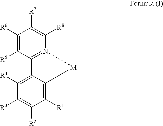
- a first aspect of the invention provides an organic electroluminescent device including a luminescent layer produced by a vapor-deposition method (a vapor-deposition luminescent layer) disposed between a pair of electrodes, the luminescent layer containing at least one host material and at least one metal complex including a partial structure represented by formula (I):
- R 1 , R 2 and R 4 to R 8 each independently represent a hydrogen atom or a substituent
- R 3 represents a group represented by formula (II), an alkoxy group or an aryloxy group:
- R 11 to R 13 each independently represent a hydrogen atom or a substituent, provided that at least two of them each independently represent an alkyl group or an aryl group.
- a second aspect of the invention provides a process for producing an organic electroluminescent device including a luminescent layer disposed between a pair of electrodes, the process including vapor-depositing at least one host material and at least one metal complex including a partial structure represented by formula (I) to form the luminescent layer:
- R 1 , R 2 and R 4 to R 8 each independently represent a hydrogen atom or a substituent
- R 3 represents a group represented by formula (II), an alkoxy group or an aryloxy group:
- R 11 to R 13 each independently represent a hydrogen atom or a substituent, provided that at least two of them each independently represent an alkyl group or an aryl group.
- the organic electroluminescent device of the invention is an organic electroluminescent device having a luminescent layer produced by a vapor-deposition method, and the luminescent layer contains a metal complex including a partial structure represented by formula (I) (hereinafter, simply sometimes referred to as a metal complex).
- the luminescent layer is produced by a vapor-deposition method and contains a metal complex including a partial structure represented by formula (I) (hereinafter, simply sometimes referred to as partial structure (I)), whereby the advantages of the invention can be exerted; namely, a luminescent device can be provided that has luminescent efficiency and brightness maintained at high levels and has considerably high driving durability.
- a metal complex including a partial structure represented by formula (I) (hereinafter, simply sometimes referred to as partial structure (I)), whereby the advantages of the invention can be exerted; namely, a luminescent device can be provided that has luminescent efficiency and brightness maintained at high levels and has considerably high driving durability.
- the metal complex including partial structure (I) will be described in detail below.
- M represents a metal.
- the metal is not particularly limited, and is preferably one selected from the group consisting of a rare earth metal, Ru, Rh, Pd, Ag, W, Re, Os, Ir, Pt and Au, and is more preferably Ir or Pt.
- R 1 , R 2 and R 4 to R 8 each independently represent a hydrogen atom or a substituent.
- R 1 , R 2 and R 4 to R 8 examples include an alkyl group (preferably having 1 to 30 carbon atoms, more preferably having 1 to 20 carbon atoms, and particularly preferably having 1 to 10 carbon atoms, such as methyl, ethyl, isopropyl, tert-butyl, n-octyl, n-decyl, n-hexadecyl, cyclopropyl, cyclopentyl, cyclohexyl, trifluoromethyl, and pentafluoromethyl); an alkenyl group (preferably having 2 to 30 carbon atoms, more preferably having 2 to 20 carbon atoms, and particularly preferably having 2 to 10 carbon atoms, such as vinyl, allyl, 2-butenyl, and 3-pentenyl); an alkynyl group (preferably having 2 to 30 carbon atoms, more preferably having 2 to 20 carbon atoms, and particularly preferably having 2 to 10 carbon atoms, such as vinyl
- R 1 , R 2 and R 4 to R 8 are preferably each independently selected from a hydrogen atom, an alkyl group, an aryl group, an alkoxy group, an aryloxy group, a heterocyclic group, a silyl group and a halogen atom or form a benzo condensed ring structure by bonding two of the substituents, and are more preferably each independently a hydrogen atom, an alkyl group having 1 to 10 carbon atoms, an aryl group having 6 to 12 carbon atoms, an alkoxy group having 1 to 10 carbon atoms, an aryloxy group having 6 to 12 carbon atoms, a heterocyclic group having 1 to 12 carbon atoms containing a nitrogen atom, an oxygen atom or a sulfur atom as a heteroatom, a fluorine atom or a chlorine atom.
- R 1 , R 2 and R 4 to R 8 are each a hydrogen atom. It is also preferable that two of R 5 to R 8 which are adjacent to each other are bonded to each other to form a benzo condensed ring structure, and more preferable that R 5 and R 6 are bonded to each other to form a benzo condensed ring structure. Further, it is preferable that at least one of R 1 , R 2 , and R 4 is a fluorine atom, and more preferable that R 2 and R 4 each are a fluorine atom.
- R 3 represents a group represented by the formula (II), an alkoxy group or an aryloxy group.
- R 11 to R 13 each independently represent a hydrogen atom or a substituent, provided that at least two of them each independently represent an alkyl group or an aryl group.
- R 11 to R 13 are the same as the substituent for R 1 , and the preferred range thereof is also the same. At least two of R 11 to R 13 may be bonded to each other to form a ring.
- the alkoxy group and the aryloxy group for R 3 are the same as the alkoxy group and the aryloxy group for R 1 , and the preferred range thereof is also the same.
- R 3 is preferably a group represented by formula (II), more preferably at least two of R 11 to R 13 in formula (II) each are an alkyl group, and yet more preferably each of R 11 to R 13 are an alkyl group.
- the alkyl group herein is the same as the alkyl group for R 1 , and is preferably an alkyl group having 1 to 10 carbon atoms, and more preferably an alkyl group having 1 to 5 carbon atoms (such as methyl, ethyl, propyl, isopropyl, t-butyl or neopentyl).
- R 3 is preferably a tertiary alkyl group (such as t-butyl, 1,1-dimethylpropyl, 1,1,3,3-tetramethylbutyl or 1-methylcyclopropyl), more preferably a tertiary alkyl group having 4 to 30 carbon atoms, and most preferably a tertiary alkyl group having 5 to 20 carbon atoms.
- a tertiary alkyl group such as t-butyl, 1,1-dimethylpropyl, 1,1,3,3-tetramethylbutyl or 1-methylcyclopropyl
- R 3 is preferably a tertiary alkyl group (such as t-butyl, 1,1-dimethylpropyl, 1,1,3,3-tetramethylbutyl or 1-methylcyclopropyl), more preferably a tertiary alkyl group having 4 to 30 carbon atoms, and most preferably a tertiary alkyl group having
- Example compounds of the metal complex in the invention are shown below, but the invention is not limited thereto.
- the metal complex in the invention can be synthesized using various methods.
- a ligand or a dissociated product thereof can be synthesized by reacting a ligand or a dissociated product thereof with a metallic compound in the presence or absence of a solvent (such as a halogen solvent, an alcohol solvent, an ether solvent, an ester solvent, a ketone solvent, a nitrile solvent or water) or in the presence or absence of a base (including various inorganic and organic bases, such as sodium methoxide, t-butoxypotassium, triethylamne or potassium carbonate) at room temperature or lower or under heating (in which a heating method using microwaves is also effective in addition to the ordinary heating method).
- a solvent such as a halogen solvent, an alcohol solvent, an ether solvent, an ester solvent, a ketone solvent, a nitrile solvent or water
- a base including various inorganic and organic bases, such as sodium methoxide, t-butoxypotassium, triethylamne or potassium carbon
- the luminescent device including the metal complex in the invention will be described.
- the luminescent device of the invention is not particularly limited in system, driving method and use mode, insofar as the device utilizes the metal complex including partial structure (I).
- Representative examples of the luminescent device include an organic EL (electroluminescent) device.
- the luminescent device of the invention includes a pair of electrodes, i.e., a positive electrode and a negative electrode, between which at least a luminescent layer is provided, and the device may further include other layers by forming plural organic compound layers including the luminescent layer.
- a hole transport layer is preferably provided, and furthermore, a hole injection layer, an electron injection layer, an electron transport layer and a protective layer may be provided.
- a hole injection layer, an electron injection layer, an electron transport layer and a protective layer may be provided.
- Each of these layers may also have other functions, and layers having the same function may be accumulated.
- the layers may be formed by using various kinds of materials.
- the positive electrode supplies holes to the hole injection layer, the hole transport layer, and/or the luminescent layer.
- the positive electrode can be made from a metal, an alloy, a metal oxide, an electrically conductive compound, or a mixture thereof, and is preferably made of a material having a work function of 4 eV or more.
- the material of the positive electrode include electrically conductive metal oxides such as tin oxide, zinc oxide, indium oxide, and ITO; metals such as gold, silver, chromium, and nickel; mixtures and laminated products of these metals and the electrically conductive metal oxides; electrically conductive inorganic substances such as copper iodide, and copper sulfide; electrically conductive organic substances such as polyaniline, polythiophene, and polypyrrole; and laminated products of the electrically conductive organic substances and ITO.
- the material of the positive electrode is preferably an electrically conductive metal oxide.
- the material is more preferably ITO from the viewpoints of productivity, high electrical conductivity, transparency and the like.
- the thickness of the positive electrode can be suitably determined according to the material of the positive electrode, but is preferably 10 nm to 5 ⁇ m, more preferably 50 nm to 1 ⁇ m, and still more preferably 100 to 500 nm.
- the positive electrode is usually an article having a layer of at least one of the above-described materials on a substrate made of soda lime glass, no-alkali glass, or a transparent resin.
- the substrate is made of glass
- the glass is preferably no-alkali glass in order to reduce ions deriving from the glass.
- the substrate is made of soda lime glass
- the substrate is preferably coated with a barrier coating such as silica.
- the transparent resin substrate include polymeric materials including polyesters such as polyethylene terephthalate, polybutylene terephthalate and polyethylene naphthalate, polyethylene, polycarbonate, polyethersulfone, polyarylate, allyldiglycolcarbonate, polyimide, polycycloolefin, norbornene resins, poly(chloro-trifluoroethylene), TEFRON (polytetrafluoroethylene) and polytetrafluoroethylene-polyethylene copolymers.
- polyesters such as polyethylene terephthalate, polybutylene terephthalate and polyethylene naphthalate
- polyethylene polycarbonate
- polyethersulfone polyarylate
- allyldiglycolcarbonate polyimide
- polycycloolefin norbornene resins
- poly(chloro-trifluoroethylene) poly(chloro-trifluoroethylene)
- TEFRON polytetrafluoroethylene
- the thickness of the substrate is not limited, as long as the substrate has sufficient mechanical strength. However, when the substrate is made of glass, the thickness thereof is generally 0.2 mm or more, and preferably 0.7 mm or more.
- a method for producing a positive electrode is selected according to the material of the positive electrode.
- the ITO film may be formed by an electron beam method, a sputtering method, a resistance heating deposition method, a chemical reaction method (e.g., a sol-gel method), or a method of applying a dispersion of indium tin oxide.
- the positive electrode can be subjected to washing or other treatment to lower the driving voltage of the device and/or to enhance luminescence efficiency.
- the positive electrode is made of ITO, for example, UV-ozone treatment or plasma treatment is effective.
- the negative electrode supplies electrons to the electron injection layer, the electron transport layer, and/or the luminescent layer
- the material of the negative electrode is selected in consideration of adhesion between the negative electrode and a layer adjacent to the negative electrode, such as the electron injection layer, the electron transport layer, and/or the luminescent layer, and ionization potential and stability of the material.
- the negative electrode can be made from a metal, an alloy, a metal halide, a metal oxide, an electrically conductive compound, or a mixture thereof.
- the material of the negative electrode include alkali metals such as lithium, sodium, potassium, and fluorides and oxides thereof; alkaline earth metals such as magnesium, calcium, and fluorides and oxides thereof; gold, silver, lead, aluminum, a sodium-potassium alloy, and mixed metals of these materials; a lithium-aluminum alloy and mixed metals including the lithium-aluminum alloy; a magnesium-silver alloy and mixed metals including the magnesium-silver alloy; and rare earth metals such as indium and ytterbium.
- the negative electrode is preferably made of a material selected from the above materials and has a work function of 4 eV or less.
- the material of the negative electrode is more preferably aluminum, a lithium-aluminum alloy or a mixed metal including the lithium-aluminum alloy, or a magnesium-silver alloy or a mixed metal including the magnesium-silver alloy.
- the negative electrode can be one layer of any of the above-described materials or multilayers including one or more of the above-described materials.
- the negative electrode preferably has a layered structure of aluminum/lithium fluoride, or aluminum/lithium oxide.
- the thickness of the negative electrode can be suitably determined according to the material of the negative electrode. However, the thickness is preferably 10 nm to 5 ⁇ m, more preferably 50 nm to 1 ⁇ m, and still more preferably 100 nm to 1 ⁇ m.
- the negative electrode is formed by an electron beam method, a sputtering method, a resistance heating deposition method, a coating method, or a transferring method.
- One metal can be vapor-deposited, or at least two metals can be vapor-deposited simultaneously.
- In order to form an alloy electrode at least two metals can be vapor-deposited simultaneously, or an alloy prepared in advance can be vapor-deposited.
- the sheet resistance of each of the positive and negative electrodes is preferably low, and, specifically, is preferably several hundred ohm/sq or less.
- the materials of the luminescent layer are materials that can form a layer having a function of receiving holes from the positive electrode, the hole injection layer or the hole transport layer and receiving electrons from the negative electrode, the electron injection layer or the electron transport layer when an electric field is applied to the device, a function of transporting the injected charges and a function of providing a field where holes are recombined with electrons to emit light.
- the luminescent layer may be made of a single substance or a combination of plural substances.
- a charge transport material is doped with a luminescent material as a dopant, either to obtain superior performance by separating the charge transporting function and the luminescent function, or to prevent the phenomenon of radiationless quenching (concentration quenching) from occurring, whereby aggregation occurs in the luminescent material at a high concentration and deactivates the excited state without radiation.
- the luminescent layer of the invention containing the metal complex including partial structure (I) and the host material preferably contains the metal complex in a concentration of from 1 to 15% by mass, more preferably from 2 to 10% by mass, and yet more preferably from 3 to 8% by mass.
- the concentration of the metal complex is less than the above-described range, there may be cases where sufficient luminescent brightness cannot be obtained, and the host material is liable to emit light at an undesirable wavelength.
- the concentration of the metallic complex exceeds the above-described range, the luminescent efficiency is liable to deteriorate due to concentration quenching, and the charges flow in the metallic complex making it liable to decompose, whereby driving durability tends to deteriorate.
- the metal complex may be used singly or in combination of plural kinds thereof.
- the luminescent layer contains the host material in addition to the metal complex of the invention, and from the standpoint of holes and/or electrons transport properties, the luminescent layer preferably contains, for example, at least one kind of the host material selected from the group consisting of a carbazole derivative (described, for example, in Applied Physics Letters, Vol. 74, No. 3, p. 442 (1999)), a tribenzoazepine derivative (described in JP-A Nos. 10-59943, 10-219241, 10-316875, 10-324680, 10-330365 and 2001-97953), a triazole derivative (described in U.S. Pat. No. 3,112,197), an oxazole derivative (described in U.S. Pat. No.
- a heterocyclic tetracarboxylic anhydride derivative (described in Japanese Journal of Applied Physics, Vol. 27, L269 (1988)), porphyrin and a phthalocyanine derivative (described in JP-A No. 63-2956965), a metal complex of an 8-quinolinol derivative (described in IEICE Transactions (The Institute of Electronics, Information and Communication Engineers (Japan)), 1990, C-2, p. 661), a metal complex having benzoxazole as a ligand, and a metal complex having benzothiazole as a ligand (the disclosures of the above patent documents and the above literatures being incorporated by reference herein).
- a carbazole derivative is more preferably used.
- the energy level of the minimum triplet excited state (T 1 level) of the host material is higher than the T 1 level of the luminescent material.
- the T 1 level of the luminescent material is higher when the luminescent wavelength thereof is shorter, and thus a host material having a high T 1 level is necessary in a luminescent layer of a luminescent device for a short wavelength.
- the T 1 level relates to the highest occupied molecular orbital (HOMO) and the lowest unoccupied molecular orbital (LUMO) of the host material, which relate to the capabilities of injection and transport of the charge (i.e., in general, when the energy difference between HOMO and LUMO is larger, it is difficult for the charge to be injected, and electric insulation increases). Accordingly, it is important that a host material having the optimum T 1 level is selected.
- HOMO highest occupied molecular orbital
- LUMO lowest unoccupied molecular orbital
- the host material for the luminescent layer for a blue luminescent device having a luminescent maximum wavelength of 500 nm or less preferably has a T 1 level of 62 kcal/mol or more (259 kJ/mol or more) and 85 kcal/mol or less (355 kJ/mol or less), and more preferably 65 kcal/mol or more (272 kJ/mol or more) and 80 kcal/mol or less (334 kJ/mol or less).
- the host material for the luminescent device of the invention that satisfies the above-described values, the host materials disclosed in JP-A Nos. 2002-100476 and 2002-338579, the disclosures of which are incorporated by reference herein, are preferred, and the host materials disclosed in JP-A No. 2002-100476 are more preferred.
- the preferred range of the host materials disclosed in JP-A No. 2002-100476 is as described therein.
- the luminescent layer of the invention is produced by a vapor-deposition method.
- the vapor-deposition method is generally such that a substance is evaporated by heating under a high vacuum (10 ⁇ 2 Pa or less), and the vaporized substance is deposited on a target to form a layer.
- Examples of the heating method for evaporating a substance from an evaporation source include a resistance heating method, a high-frequency heating method, an electron beam heating method and a laser heating method, and a resistance heating method is most ordinarily used.
- Examples of a method for evaporating a substance other than heating include a sputtering method, an ion plating method and a molecular beam epitaxy method, which may be selected according to purpose.
- a CVD method in which a layer is formed through chemical reaction on a surface of a target, is also included in the vapor-deposition method in the broad sense, and the vapor-deposition method referred in the invention encompasses all of these vapor-deposition techniques.
- the vapor-deposition method is described in detail in “Shinban Shinku Handbook (Vacuum Handbook, New Edition)”, Chapter 8, edited by Ulvac, Inc., published by Ohmsha, Ltd., the disclosure of which is incorporated by reference herein.
- a luminescent layer produced by the vapor-deposition method is excellent in luminescent brightness and driving durability in comparison to a luminescent layer produced by the wet film forming method, represented by a spin coating method and an inkjet method, because the layer is free from impurities, oxygen and water derived from the solvent or the binder, and furthermore, such a layer is free from a problem wherein a lower layer that has already been formed is dissolved by the solvent. Accordingly, a uniform luminescent layer having a desired thickness can be easily obtained.
- the luminescent layer produced by the vapor-deposition method is suitable for producing a full-color display with high precision and high image quality because different luminescent materials and host materials may be used for the respective pixels to impart different luminescent capabilities thereto.
- the material of the luminescent layer contains only materials having a molecular weight of 3,000 or less.
- polymeric materials including polymers and oligomers are not preferred because they are difficult to be vapor-deposited due to their low volatility, and are difficult to provide luminescence with good reproducibility due to the molecular weight distribution of the materials.
- the metal complex including partial structure (I) preferably has a molecular weight of 3,000 or less, and in cases where the luminescent layer contains other materials including the host material, the materials each preferably have a molecular weight of 3,000 or less. It is more preferable that all the materials contained in the luminescent layer each have a molecular weight of from 200 to 2,000.
- a high molecular weight compound having a molecular weight exceeding 3,000 tends to be difficult to evaporate under heat even in a high vacuum environment, and thus it tends to be difficult to form a layer by the vapor-deposition method.
- the material for the luminescent layer is preferably a neutral molecular compound rather than an ionic compound from the standpoint of easiness of deposition.
- the luminescent layer produced by vapor-deposition is preferably a uniform amorphous film free from defects such as detachment and pinholes, and preferably has a high melting point and a high glass transition temperature (Tg) in view of the fact that the performance of the luminescent device is altered or deteriorated when recrystallization occurs with the lapse of time or under heat.
- the material for the luminescent layer preferably has a melting point of 150° C. or more, more preferably 200° C. or more, and yet more preferably 250° C. or more, and preferably has Tg of 70° C. or more, more preferably 100° C. or more, and yet more preferably 120° C. or more.
- a carbazole derivative is most preferred since it has a high T 1 level, tends not to suffer crystallization, and has a long life of the excited state such that high luminescent efficiency can be expected.
- the luminescent layer may contain polyphenyl, diphenylbutadiene, tetraphenylbutadiene, naphthalimide (described in JP-A No. 2-305886), coumarin, perylene (described in JP-A No. 2-189890), perynone, oxadiazole (described in JP-A No. 2-216791, or an oxadiazole derivative disclosed by Hamada, et al. in The 38th JSAP (the Japan Society of Applied Physics) Annual Meeting), an aldazine derivative (described in JP-A No. 2-220393) pyrazoline (described in JP-A No.
- the thickness of the luminescent layer is not particularly limited, and in general, it is preferably from 1 nm to 5 ⁇ m, more preferably from 5 nm to 1 ⁇ m, and yet more preferably from 10 to 500 nm.
- the luminescent layer may be constituted by a single layer or plural layers. Each of the plural layers may emit light with different luminescent colors to form white light in total, and the single luminescent layer may emit light with white light. In the case where the luminescent device includes plural luminescent layers, each of the luminescent layers may be formed with a single material or with plural compounds.
- the material of the hole injection layer and the hole transport layer may have at least one of a function for receiving holes from the positive electrode, a function for transporting holes, and a function for blocking electrons injected from the negative electrode.
- the material of the hole injection layer and the hole transport layer is preferably at least one kind selected from the group consisting of a tribenzoazepine derivative, a triazole derivative, an oxazole derivative, an oxadiazole derivative, an imidazole derivative, a polyarylalkane derivative, a polyarylbenzene derivative, an arylamine derivative, a styrylanthracene derivative, a stilbene derivative, an aromatic tertiary amine derivative, a styrylamine derivative, an aromatic dimethylidyne derivative, a metal complex of 8-quinolinol derivative, a pyrazoline derivative, a pyrazolone derivative, a phenylenediamine derivative, an amino-substituted chalcone derivative, a fluorenone derivative, a hydrazone derivative, a silazane derivative and a porphyrin derivative.
- Preferred examples of these compounds include the corresponding compounds described for the host material.
- the energy level of the minimum triplet excited state (T 1 level) of the hole transport material is higher than the T 1 levels of the luminescent material and the host material of the luminescent layer for preventing triplet excitons generated in the luminescent layer from migrating to the hole transport layer.
- the T 1 level of the hole transport material for a blue luminescent device having a luminescent maximum wavelength of 500 nm or less is preferably 62 kcal/mol or more (259 kJ/mol or more) and 85 kcal/mol or less (355 kJ/mol or less), and more preferably 65 kcal/mol or more (272 kJ/mol or more) and 80 kcal/mol or less (334 kJ/mol or less).
- the hole transport materials disclosed in JP-A No. 2002-100476 are preferred, and the preferred range of the hole transport materials disclosed in JP-A No. 2002-100476 is as described therein.
- a tribenzoazepine derivative is expected to provide high luminescent efficiency owing to the high T 1 level thereof, and an arylamine derivative is expected to provide improved durability owing to the high stability thereof. Therefore, the hole transport material is preferably selected from these compounds.
- such compounds may be added, depending on necessity, as carbazole, a polysilane compound, an electroconductive polymer or oligomer, such as poly(N-vinylcarbazole), an aniline copolymer and a thiophene oligomer, an organic silane, a carbon film, and derivatives thereof.
- the thickness of the hole injection layer is not particularly limited, and in general, it is preferably from 0.2 nm to 1 ⁇ m, more preferably from 1 nm to 0.2 ⁇ m, and still more preferably from 2 to 100 nm.
- the thickness of the hole transport layer is not particularly limited, and in general, it is preferably from 1 nm to 5 ⁇ m, more preferably from 5 nm to 1 ⁇ m, and still more preferably from 10 to 500 nm.
- the hole injection layer and the hole transport layer may have a single layer structure containing one or plural kinds of the above-described compounds, or may have a multilayer structure having plural layers each having the same composition or different compositions.
- the hole injection layer and the hole transport layer are formed by a vacuum deposition method, an LB method, a method in which a hole injection or transport material is dissolved or dispersed in a solvent and the resultant coating solution is applied to a substrate or any other layer, an ink-jet method, a printing method, or a transferring method.
- the above-described material and a resin component may be dissolved or dispersed in a solvent.
- the resin component include polyvinyl chloride, polycarbonate, polystylene, polymetyl methacrylate, polybutyl methacrylate, polyester, polysulfone, polyphenylene oxide, polybutadiene, poly(N-vinylcarbazole), hydrocarbon resins, ketone resins, phenoxy resins, polyamide, ethylcellulose, vinyl acetate resins, ABS resins, polyurethane resins, melamine resins, unsaturated polyester resins, alkyd resins, epoxy resins, and silicone resins.
- the hole transport layer is preferably formed by a vapor-deposition method.
- a layer formed by a vapor-deposition method has a uniform and constant thickness and tends to have improved durability.
- the materials of the hole transport layer are preferably low molecular weight organic compounds having a molecular weight of 3,000 or less and/or low molecular weight organic metal compounds having a molecular weight of 3,000 or less, similarly to the materials of the luminescent layer.
- the material of the electron injection layer and the electron transport layer may have at least one of a function of receiving electrons from the negative electrode, a function of transporting electrons, and a function of blocking electrons injected from the positive electrode.
- the luminescent device of the invention preferably has, between the negative electrode and the luminescent layer, a layer containing a compound having an ionization potential of 5.9 eV or more (more preferably 6.0 eV or more), and more preferably has an electron transport layer having an ionization potential of 5.9 eV or more.
- That compound include triazole, oxazole, oxadiazole, imidazole, fluorenone, anthraquinodimethane, anthrone, diphenylquinone, thiopyran dioxide, carbodiimide, fluorenylidene methane, distyrylpyrazine, aromatic tetracarboxlic acid anhydride such as naphthalene tetracarboxylic acid anhydride and perylene tetracarboxylic acid anhydride, phthalocyanine, various metallic complexes represented by a metal complex of a 8-quinolinol and a metal complex having metalphthalocyanine benzoxazole or benzothiazole as a ligand, an organic silane, and derivatives thereof.
- Preferred examples of these compounds include the preferred examples of the corresponding compounds described for the host material.
- a layer containing such a compound i.e., a blocking layer
- reduction in luminescent efficiency and deterioration in durability caused by holes penetrating through the luminescent layer and flowing into the electron transport layer can be prevented from occurring.
- the energy level of the minimum triplet excited state (T 1 level) of the electron transport material is higher than the T 1 levels of the luminescent material and the host material of the luminescent layer for preventing triplet excitons generated in the luminescent layer from migrating to the electron transport layer.
- the T 1 level of the electron transport material for a blue luminescent device having a luminescent maximum wavelength of 500 nm or less is preferably 62 kcal/mol or more (259 kJ/mol or more) and 85 kcal/mol or less (355 kJ/mol or less), and more preferably 65 kcal/mol or more (272 kJ/mol or more) and 80 kcal/mol or less (334 kJ/mol or less).
- the electron transport materials disclosed in JP-A No. 2002-100476 are preferred, and the preferred range of the electron transport materials disclosed in JP-A No. 2002-100476 is as described therein.
- such compounds may be added, depending on necessity, as carbazole, a polysilane compound, an electroconductive polymer or oligomer, such as poly(N-vinylcarbazole), an aniline copolymer and a thiophene oligomer, an organic silane, a carbon film, and derivatives thereof.
- the thickness of the electron injection layer is not particularly limited, and in general, it is preferably from 0.2 nm to 1 ⁇ m, more preferably from 1 nm to 0.2 ⁇ m, and still more preferably from 2 to 100 nm.
- the thickness of the electron transport layer is not particularly limited, and in general, it is preferably from 1 nm to 5 ⁇ m, more preferably from 5 nm to 1 ⁇ m, and still more preferably from 10 to 500 nm.
- the electron injection layer and the electron transport layer may have a single layer structure containing one or plural kinds of the above-described compounds, or may have a multilayer structure having plural layers each having the same composition or different compositions.
- the electron injection layer and the electron transport layer are formed by a vacuum deposition method, an LB method, a method in which an electron injection or transport material is dissolved or dispersed in a solvent and the resultant coating solution is applied to a substrate or any other layer, an ink-jet method, a printing method, or a transferring method.
- the above-described material and a resin component may be dissolved or dispersed in a solvent.
- the resin component include those exemplified for the hole injection layer.
- the electron transport layer is preferably formed by a vapor-deposition method.
- a layer formed by a vapor-deposition method has a uniform and constant thickness and tends to have improved durability.
- the materials of the electron transport layer are preferably low molecular weight organic compounds having a molecular weight of 3,000 or less and/or low molecular weight organic metal compounds having a molecular weight of 3,000 or less, similarly to the materials of the luminescent layer.
- the luminescent device of the invention may include a protective layer to prevent moisture and oxygen from entering the device.
- the material of the protective layer may have a function of preventing substances that accelerate deterioration of the device, such as moisture and oxygen, from entering the device.
- metals such as In, Sn, Pb, Au, Cu, Ag, Al, Ti and Ni
- metal oxides such as MgO, SiO, SiO 2 , Al 2 O 3 , GeO, NiO, CaO, BaO, Fe 2 O 3 , Y 2 O 3 and TiO 2
- metal fluorides such as MgF 2 , LiF, AlF 3 and CaF 2
- nitrides such as SiN x and SiO x N y
- the method for forming the protective layer is not particularly limited. Examples thereof include a vacuum deposition method, a sputtering method, a reactive sputtering method, a molecular beam epitaxy (MBE) method, a cluster ion beam method, an ion-plating method, a plasma polymerization method (radio frequency excitation ion-plating method), a plasma CVD method, a laser CVD method, a thermal CVD method, a gas source CVD method, a coating method, a printing method, and a transferring method.
- MBE molecular beam epitaxy
- the method for producing an organic electroluminescent device of the invention is a method for producing an organic electroluminescent device including a luminescent layer disposed between a pair of electrodes, and the method includes vapor-depositing at least one host material and at least one metal complex including partial structure (I) to form the luminescent layer.
- a substrate having an ITO thin film as a transparent electrode is cleaned with a solvent and then subjected to a UV-ozone treatment.
- a hole injection layer and a hole transport layer are formed on the transparent electrode in this order by a vapor-deposition method.
- a metal complex and a host material are co-vapor-deposited in vacuum thereon to form a luminescent layer.
- the metal complex and the host material herein are the same as those described above, and the preferred ranges thereof are also the same.
- the host material and the metal complex used in the luminescent layer preferably have a molecular weight of 3,000 or less, and the materials used to form the luminescent layer preferably have a molecular weight of 3,000 or less. In cases where the materials have a molecular weight within this range, vapor-deposition of the materials can be facilitated.
- any known vapor-deposition method may be used.
- An electron transport layer and an electron injection layer are formed thereon.
- a patterned mask is placed on the electron injection layer, and a back electrode (negative electrode) is formed thereon by vapor-deposition.
- a blocking layer containing an electron transport material may be provided between the electron transport layer and the luminescent layer. Lead wires are connected to the positive electrode and the negative electrode, respectively, so as to produce a luminescent accumulated body. The resultant accumulated body is sealed to fabricate a luminescent device.
- the luminescent device is made to emit light by applying a direct current voltage, and the initial luminescent capability can be measured.
- the driving durability of the luminescent device can be measured and evaluated in terms of a half-value period where the initial brightness is reduced by half.
- the luminescent device of the invention can be suitably used in the fields of display devices, displays, backlights, electrophotography, light sources for illumination, light sources for recording, light sources for exposure, light sources for reading, signs, sign boards, interiors, optical communications, and the like.
- the ITO thin film had a surface resistance of 10 ⁇ /sq.
- the substrate having the transparent electrode formed thereon was washed with EPA in a cleaning vessel, and then subjected to UV-ozone treatment for 30 minutes.
- a hole injection layer was provided by depositing copper phthalocyanine on the transparent electrode by a vacuum deposition method to a thickness of 0.01 ⁇ m at a rate of 0.1 nm/sec.
- a hole transport layer was then provided thereon by depositing N,N′-dinaphthyl-N,N′-diphenylbenzidine (NPD) by a vacuum deposition method to a thickness of 0.03 ⁇ m at a rate of 0.1 nm/sec.
- NPD N,N′-dinaphthyl-N,N′-diphenylbenzidine
- iridium complex as a luminescent material (dopant) and a host material shown in Table 1 below were co-vapor-deposited thereon at rates of 0.015 nm/sec and 0.3 nm/sec, respectively, to form a luminescent layer having a thickness of 0.03 ⁇ m.
- a blocking layer was provided thereon by using aluminum(III) bis(2-methyl-8-quinolinato)4-phenylphenolate (Balq 2 ) as an electron transport material to a thickness of 0.01 ⁇ m at a rate of 0.3 nm/sec.
- An electron transport layer was further provided thereon by using tris(8-hydroxyquinolinato)aluminum (Alq 3 ) as an electron transport material to a thickness of 0.04 ⁇ m at a rate of 0.2 nm/sec.
- An electron injecting layer was further provided thereon by using LiF to a thickness of 0.002 ⁇ m at a rate of 0.001 nm/sec.
- a patterned mask with a square opening to give a luminescent area of 5 mm ⁇ 5 mm was placed on the electron injection layer, and a back electrode (negative electrode) was formed thereon by vapor-depositing aluminum to a thickness of 0.25 ⁇ m in a deposition apparatus.
- Aluminum lead wires were connected to the transparent electrode (which functioned as a positive electrode) and the back electrode, respectively, so as to produce a luminescent accumulated body.
- the resultant luminescent accumulated body was placed in a glove box substituted with nitrogen gas.
- 10 mg of calcium oxide powder as a water adsorbing agent were placed in a stainless-steel sealing cover having a recession inside, and the sealing cover was fixed with an adhesive tape.
- the luminescent accumulated body was sealed by using the sealing cover and an ultraviolet ray-curable adhesive (XNR5516HV, produced by Nagase Chemtex Corporation) to produce luminescent devices of Examples 1 to 6 and Comparative Examples 1 to 5.
- the luminescent devices thus obtained were evaluated in the following manner.
- the organic EL device to be evaluated was applied with a direct current voltage by using Source-Measure Unit Model 2400, produced by TOYO Corp. to emit light, and the initial luminescent capability was measured.
- the maximum brightness was designated as Lmax (Cd/M 2 ), and the voltage providing Lmax was designated as Vmax (V).
- the luminescent efficiency at 1,000 Cd/m 2 was evaluated as an external quantum efficiency ( ⁇ 1000 ) (%), and shown in Table 1.
- a driving durability test was carried out at an initial brightness of 1,000 Cd/m 2 , and the time when the initial brightness was reduced by half was designated as a half-value period (T 1/2 ) (H).
- a luminescent device of Example 7 was produced in the same manner as in Example 1 except that the hole transport layer was provided by the following wet method.
- PVK polyvinylcarbazole
- 1 mL of 1,2-dichloroethane 6 mg was dissolved in 1 mL of 1,2-dichloroethane to obtain a solution.
- the solution was coated on the hole injection layer (formed by vacuum deposition of copper phthalocyanine) by a spin coating method at a rotation rate of 1,000 rpm for 1 second to form a hole transport layer having a thickness of 0.05 ⁇ m, and further thereon, a luminescent material Ir-1 and a host material were co-vapor-deposited to form a luminescent layer.
- the resultant luminescent device was evaluated for green luminescent capability in the same manner as in Example 1. The results thus obtained are shown in Table 1.
- a luminescent device of Comparative Example 6 was produced in the same manner as in Example 1 except that the luminescent layer was provided by the following wet method.
- a host material OXD-1 2.5 ml of a host material OXD-1, 0.4 g of a luminescent material Ir-1 and 2.5 mg of polyvinylbiphenyl having a weight average molecular weight of 115,000 in polystyrene conversion as a binder polymer were dissolved in 1 mL of xylene to obtain a solution.
- the solution was coated on the hole transport layer (formed by a vacuum deposition of NPD) by a spin coating method at a rotation number of 1,000 rpm for 1 second to form a luminescent layer having a thickness of 0.02 ⁇ m, and further thereon, Balq 2 as an electron transport material was vapor-deposited to form a blocking layer.
- the resultant luminescent device was evaluated for green luminescent capability in the same manner as in Example 1. The results thus obtained are shown in Table 1.
- a luminescent device of Comparative Example 7 was produced in the same manner as in Comparative Example 6 except that the dopant Ir-1 in Comparative Example 6 was replaced by C-4.
- the resultant luminescent device was evaluated for green luminescent capability in the same manner as in Example 1. The results thus obtained are shown in Table 1.
- Example 1 It is understood from the comparison between Example 1 and Examples 6 and 7 that in cases where the host material is a material other than a carbazole derivative or in cases where the hole transport layer is formed by a wet method, reduction in brightness, increase in driving voltage, reduction in luminescent efficiency and acceleration of deterioration are slightly observed even though the luminescent layer is formed by a vapor-deposition method using the metal complex of the invention.
- the luminescent device of Comparative Example 6 having a luminescent layer formed by a wet method suffers remarkable reduction in brightness, luminescent efficiency and durability even though the metal complex including partial structure (I) of the invention is used, and there is no significant difference in capability from Comparative Example 7 due to the dopant used.
- an organic electroluminescent device can be provided that has high brightness and high luminescent efficiency with high driving durability.
Abstract

wherein M represents a metal atom, R1, R2 and R4 to R8 each independently represent a hydrogen atom or a substituent, and R3 represents a group represented by formula (II), an alkoxy group or an aryloxy group:

wherein R11 to R13 each independently represent a hydrogen atom or a substituent, provided that at least two of them each independently represent an alkyl group or an aryl group.
Description

wherein M represents a metal atom, R1, R2 and R4 to R8 each independently represent a hydrogen atom or a substituent, and R3 represents a group represented by formula (II), an alkoxy group or an aryloxy group:

wherein R11 to R13 each independently represent a hydrogen atom or a substituent, provided that at least two of them each independently represent an alkyl group or an aryl group.


| TABLE 1 | ||||||||||
| Host | Hole transport | Lmax | Vmax | η1000 | T1/2 | Luminescent layer | Hole transport layer | |||
| Dopant | material | material | (Cd/m2) | (V) | (%) | (H) | forming method | forming method | ||
| Example 1 | Ir-1 | CBP | NPD | 78,000 | 14 | 9.8 | 7,200 | vapor-deposition | vapor-deposition |
| method | method | ||||||||
| Example 2 | Ir-2 | CBP | NPD | 70,000 | 14 | 9.1 | 6,500 | vapor-deposition | vapor-deposition |
| method | method | ||||||||
| Example 3 | Ir-4 | CBP | NPD | 62,000 | 15 | 8.3 | 6,000 | vapor-deposition | vapor-deposition |
| method | method | ||||||||
| Example 4 | Ir-5 | CBP | NPD | 76,000 | 14 | 9.6 | 7,500 | vapor-deposition | vapor-deposition |
| method | method | ||||||||
| Example 5 | Ir-6 | CBP | NPD | 75,000 | 14 | 9.5 | 8,000 | vapor-deposition | vapor-deposition |
| method | method | ||||||||
| Example 6 | Ir-1 | OXD-1 | NPD | 55,000 | 16 | 7.2 | 5,000 | vapor-deposition | vapor-deposition |
| method | method | ||||||||
| Example 7 | Ir-1 | CBP | PVK | 52,000 | 17 | 6.5 | 4,200 | vapor-deposition | wet method |
| method | |||||||||
| Comparative | C-1 | CBP | NPD | 48,000 | 14 | 6.2 | 1,800 | vapor-deposition | vapor-deposition |
| Example 1 | method | method | |||||||
| Comparative | C-2 | CBP | NPD | 46,000 | 14 | 6.3 | 2,000 | vapor-deposition | vapor-deposition |
| Example 2 | method | method | |||||||
| Comparative | C-3 | CBP | NPD | 40,000 | 15 | 6 | 2,500 | vapor-deposition | vapor-deposition |
| Example 3 | method | method | |||||||
| Comparative | C-4 | CBP | NPD | 55,000 | 14 | 7 | 3,000 | vapor-deposition | vapor-deposition |
| Example 4 | method | method | |||||||
| Comparative | C-5 | CBP | NPD | 32,000 | 16 | 4.2 | 550 | vapor-deposition | vapor-deposition |
| Example 5 | method | method | |||||||
| Comparative | Ir-1 | OXD-1 | NPD | 10,000 | 18 | 1.5 | 120 | wet method | vapor-deposition |
| Example 6 | method | ||||||||
| Comparative | C-4 | OXD-1 | NPD | 9,000 | 18 | 1 | 90 | wet method | vapor-deposition |
| Example 7 | method | ||||||||


Claims (8)


Applications Claiming Priority (2)
| Application Number | Priority Date | Filing Date | Title |
|---|---|---|---|
| JP2004-189857 | 2004-06-28 | ||
| JP2004189857A JP2006013222A (en) | 2004-06-28 | 2004-06-28 | Organic electroluminescence element and method for manufacturing the same |
Publications (2)
| Publication Number | Publication Date |
|---|---|
| US20050287396A1 US20050287396A1 (en) | 2005-12-29 |
| US7745017B2 true US7745017B2 (en) | 2010-06-29 |
Family
ID=35506186
Family Applications (1)
| Application Number | Title | Priority Date | Filing Date |
|---|---|---|---|
| US11/166,158 Active 2027-06-26 US7745017B2 (en) | 2004-06-28 | 2005-06-27 | Organic electroluminescent device and method for producing the same |
Country Status (2)
| Country | Link |
|---|---|
| US (1) | US7745017B2 (en) |
| JP (1) | JP2006013222A (en) |
Cited By (20)
| Publication number | Priority date | Publication date | Assignee | Title |
|---|---|---|---|---|
| US20080297040A1 (en) * | 2007-06-01 | 2008-12-04 | Weishi Wu | Charge transport materials for luminescent applications |
| US20090058286A1 (en) * | 2006-03-27 | 2009-03-05 | Showa Denko K.K | Organic light-emitting device using a compound having a carrier transport property and a phosphorescent property |
| US20100187507A1 (en) * | 2008-12-04 | 2010-07-29 | Park Kyung-Ho | Electroactive materials |
| US20100187506A1 (en) * | 2008-12-01 | 2010-07-29 | Park Kyung-Ho | Electroactive materials |
| US20100213825A1 (en) * | 2008-12-01 | 2010-08-26 | Park Kyung-Ho | Electroactive materials |
| US20100252819A1 (en) * | 2009-04-03 | 2010-10-07 | E. I. Du Pont De Nemours And Company | Electroactive materials |
| US20110037056A1 (en) * | 2008-12-12 | 2011-02-17 | E. I. Du Pont De Nemours And Company | Photoactive composition and electronic device made with the composition |
| US20110095273A1 (en) * | 2009-09-29 | 2011-04-28 | E. I. Du Pont De Nemours And Company | Deuterated compounds for luminescent applications |
| US20120065432A1 (en) * | 2007-11-19 | 2012-03-15 | E.I Du Pont De Nemours And Company | Electroactive materials |
| US8343381B1 (en) | 2008-05-16 | 2013-01-01 | E I Du Pont De Nemours And Company | Hole transport composition |
| WO2013142634A1 (en) * | 2012-03-23 | 2013-09-26 | E. I. Du Pont De Nemours And Company | Green luminescent materials |
| WO2013142633A1 (en) * | 2012-03-23 | 2013-09-26 | E. I. Du Pont De Nemours And Company | Green luminescent materials |
| WO2013163019A1 (en) * | 2012-04-23 | 2013-10-31 | E. I. Du Pont De Nemours And Company | Blue luminescent compounds |
| WO2013163022A1 (en) * | 2012-04-23 | 2013-10-31 | E. I. Du Pont De Nemours And Company | Blue luminescent compounds |
| WO2013165118A1 (en) * | 2012-04-30 | 2013-11-07 | 율촌화학주식회사 | Novel intermetallic compound, and blue phosphorescent organic light-emitting diode including same |
| US8617720B2 (en) | 2009-12-21 | 2013-12-31 | E I Du Pont De Nemours And Company | Electroactive composition and electronic device made with the composition |
| US8759818B2 (en) | 2009-02-27 | 2014-06-24 | E I Du Pont De Nemours And Company | Deuterated compounds for electronic applications |
| KR101503767B1 (en) * | 2012-04-30 | 2015-03-19 | 율촌화학 주식회사 | The new metal complex and blue phosphorescent organic light emitting device comprising the same |
| US9293716B2 (en) | 2010-12-20 | 2016-03-22 | Ei Du Pont De Nemours And Company | Compositions for electronic applications |
| US9496506B2 (en) | 2009-10-29 | 2016-11-15 | E I Du Pont De Nemours And Company | Deuterated compounds for electronic applications |
Families Citing this family (15)
| Publication number | Priority date | Publication date | Assignee | Title |
|---|---|---|---|---|
| US7498437B2 (en) | 2005-04-27 | 2009-03-03 | Au Optronics Corporation | Phosphorescent light-emitting device with doped iridium-complex |
| JP2007059517A (en) * | 2005-08-23 | 2007-03-08 | Fujifilm Corp | Photoelectric conversion film, photoelectric conversion element, image pickup element and method of applying electric field to them |
| JP5481057B2 (en) * | 2008-11-19 | 2014-04-23 | 株式会社東芝 | Organic electroluminescence device |
| JP2010238509A (en) * | 2009-03-31 | 2010-10-21 | Sumitomo Chemical Co Ltd | Manufacturing method of organic electroluminescent element |
| EP2282358A1 (en) * | 2009-08-07 | 2011-02-09 | Solvay SA | Host material for light-emitting devices |
| KR101097313B1 (en) * | 2009-08-10 | 2011-12-23 | 삼성모바일디스플레이주식회사 | Organic light emitting device |
| WO2011024737A1 (en) | 2009-08-27 | 2011-03-03 | 独立行政法人産業技術総合研究所 | Iridium complex and light emitting material formed from same |
| EP2471889A4 (en) | 2009-08-27 | 2013-06-26 | Sumitomo Chemical Co | Metal complex composition and complex polymer |
| JP2010185068A (en) * | 2009-08-31 | 2010-08-26 | Fujifilm Corp | Organic electroluminescent device |
| KR101352116B1 (en) * | 2009-11-24 | 2014-01-14 | 엘지디스플레이 주식회사 | White Organic Light Emitting Device |
| JP5789360B2 (en) * | 2010-06-01 | 2015-10-07 | ユー・ディー・シー アイルランド リミテッド | Iridium complex mixture, organic electroluminescent device and method for producing the same |
| JP6331617B2 (en) * | 2013-04-15 | 2018-05-30 | 住友化学株式会社 | Metal complex and light emitting device using the same |
| JP6059293B2 (en) * | 2015-06-10 | 2017-01-11 | ユー・ディー・シー アイルランド リミテッド | Iridium complex mixture, organic electroluminescent device and method for producing the same |
| US11201298B2 (en) * | 2017-01-09 | 2021-12-14 | Universal Display Corporation | Organic electroluminescent materials and devices |
| KR102626926B1 (en) * | 2018-08-31 | 2024-01-19 | 삼성전자주식회사 | Organometallic compound and organic light emitting device including the same |
Citations (7)
| Publication number | Priority date | Publication date | Assignee | Title |
|---|---|---|---|---|
| US20010019782A1 (en) | 1999-12-27 | 2001-09-06 | Tatsuya Igarashi | Light-emitting material comprising orthometalated iridium complex, light-emitting device, high efficiency red light-emitting device, and novel iridium complex |
| US20020024293A1 (en) * | 2000-07-17 | 2002-02-28 | Fuji Photo Film Co., Ltd. | Light-emitting element and iridium complex |
| US20020064681A1 (en) * | 2000-09-26 | 2002-05-30 | Takao Takiguchi | Luminescence device, display apparatus and metal coordination compound |
| WO2002044189A1 (en) * | 2000-11-30 | 2002-06-06 | Canon Kabushiki Kaisha | Luminescent element and display |
| JP2002324679A (en) | 2001-04-26 | 2002-11-08 | Honda Motor Co Ltd | Organic electroluminescent element |
| US20030059646A1 (en) * | 2000-11-30 | 2003-03-27 | Canon Kabushiki Kaisha | Luminescence device and display apparatus |
| JP2004031004A (en) | 2002-06-24 | 2004-01-29 | Konica Minolta Holdings Inc | Organic electroluminescent element and display device |
-
2004
- 2004-06-28 JP JP2004189857A patent/JP2006013222A/en active Pending
-
2005
- 2005-06-27 US US11/166,158 patent/US7745017B2/en active Active
Patent Citations (7)
| Publication number | Priority date | Publication date | Assignee | Title |
|---|---|---|---|---|
| US20010019782A1 (en) | 1999-12-27 | 2001-09-06 | Tatsuya Igarashi | Light-emitting material comprising orthometalated iridium complex, light-emitting device, high efficiency red light-emitting device, and novel iridium complex |
| US20020024293A1 (en) * | 2000-07-17 | 2002-02-28 | Fuji Photo Film Co., Ltd. | Light-emitting element and iridium complex |
| US20020064681A1 (en) * | 2000-09-26 | 2002-05-30 | Takao Takiguchi | Luminescence device, display apparatus and metal coordination compound |
| WO2002044189A1 (en) * | 2000-11-30 | 2002-06-06 | Canon Kabushiki Kaisha | Luminescent element and display |
| US20030059646A1 (en) * | 2000-11-30 | 2003-03-27 | Canon Kabushiki Kaisha | Luminescence device and display apparatus |
| JP2002324679A (en) | 2001-04-26 | 2002-11-08 | Honda Motor Co Ltd | Organic electroluminescent element |
| JP2004031004A (en) | 2002-06-24 | 2004-01-29 | Konica Minolta Holdings Inc | Organic electroluminescent element and display device |
Cited By (37)
| Publication number | Priority date | Publication date | Assignee | Title |
|---|---|---|---|---|
| US8268456B2 (en) | 2006-03-27 | 2012-09-18 | Showa Denko K.K. | Organic light-emitting device using a compound having a carrier transport property and a phosphorescent property |
| US20090058286A1 (en) * | 2006-03-27 | 2009-03-05 | Showa Denko K.K | Organic light-emitting device using a compound having a carrier transport property and a phosphorescent property |
| US20080297040A1 (en) * | 2007-06-01 | 2008-12-04 | Weishi Wu | Charge transport materials for luminescent applications |
| US8460802B2 (en) | 2007-06-01 | 2013-06-11 | E I Du Pont De Nemours And Company | Charge transport materials for luminescent applications |
| US8241762B2 (en) | 2007-06-01 | 2012-08-14 | E I Du Pont De Nemours And Company | Charge transport materials for luminescent applications |
| US8889269B2 (en) | 2007-11-19 | 2014-11-18 | E I Du Pont De Nemours And Company | Electroactive materials |
| US8652655B2 (en) * | 2007-11-19 | 2014-02-18 | E I Du Pont De Nemours And Company | Electroactive materials |
| US20120065432A1 (en) * | 2007-11-19 | 2012-03-15 | E.I Du Pont De Nemours And Company | Electroactive materials |
| US9574084B2 (en) | 2008-05-16 | 2017-02-21 | E I Du Pont De Nemours And Company | Hole transport composition |
| US8343381B1 (en) | 2008-05-16 | 2013-01-01 | E I Du Pont De Nemours And Company | Hole transport composition |
| US8551624B2 (en) | 2008-12-01 | 2013-10-08 | E I Du Pont De Nemours And Company | Electroactive materials |
| US9099653B2 (en) | 2008-12-01 | 2015-08-04 | E I Du Pont De Nemours And Company | Electroactive materials |
| US20100187506A1 (en) * | 2008-12-01 | 2010-07-29 | Park Kyung-Ho | Electroactive materials |
| US20100213825A1 (en) * | 2008-12-01 | 2010-08-26 | Park Kyung-Ho | Electroactive materials |
| US8420232B2 (en) | 2008-12-04 | 2013-04-16 | E I Du Pont De Nemours And Company | Binaphthyl-arylamine polymers |
| US20100187507A1 (en) * | 2008-12-04 | 2010-07-29 | Park Kyung-Ho | Electroactive materials |
| US20110037056A1 (en) * | 2008-12-12 | 2011-02-17 | E. I. Du Pont De Nemours And Company | Photoactive composition and electronic device made with the composition |
| US8890131B2 (en) | 2009-02-27 | 2014-11-18 | E I Du Pont De Nemours And Company | Deuterated compounds for electronic applications |
| US8759818B2 (en) | 2009-02-27 | 2014-06-24 | E I Du Pont De Nemours And Company | Deuterated compounds for electronic applications |
| US8497495B2 (en) | 2009-04-03 | 2013-07-30 | E I Du Pont De Nemours And Company | Electroactive materials |
| US20100252819A1 (en) * | 2009-04-03 | 2010-10-07 | E. I. Du Pont De Nemours And Company | Electroactive materials |
| US20110095273A1 (en) * | 2009-09-29 | 2011-04-28 | E. I. Du Pont De Nemours And Company | Deuterated compounds for luminescent applications |
| US8431245B2 (en) | 2009-09-29 | 2013-04-30 | E. I. Du Pont De Nemours And Company | Deuterated compounds for luminescent applications |
| US9496506B2 (en) | 2009-10-29 | 2016-11-15 | E I Du Pont De Nemours And Company | Deuterated compounds for electronic applications |
| US8617720B2 (en) | 2009-12-21 | 2013-12-31 | E I Du Pont De Nemours And Company | Electroactive composition and electronic device made with the composition |
| US9293716B2 (en) | 2010-12-20 | 2016-03-22 | Ei Du Pont De Nemours And Company | Compositions for electronic applications |
| WO2013142633A1 (en) * | 2012-03-23 | 2013-09-26 | E. I. Du Pont De Nemours And Company | Green luminescent materials |
| US20150028321A1 (en) * | 2012-03-23 | 2015-01-29 | E I Du Pont De Nemours And Company | Green luminescent materials |
| US20150048340A1 (en) * | 2012-03-23 | 2015-02-19 | E I Du Pont De Nemours And Company | Green luminescent materials |
| WO2013142634A1 (en) * | 2012-03-23 | 2013-09-26 | E. I. Du Pont De Nemours And Company | Green luminescent materials |
| US9735375B2 (en) * | 2012-03-23 | 2017-08-15 | E I Du Pont De Nemours And Company | Green luminescent materials |
| US9793497B2 (en) * | 2012-03-23 | 2017-10-17 | E I Du Pont De Nemours And Company | Green luminescent materials |
| WO2013163022A1 (en) * | 2012-04-23 | 2013-10-31 | E. I. Du Pont De Nemours And Company | Blue luminescent compounds |
| WO2013163019A1 (en) * | 2012-04-23 | 2013-10-31 | E. I. Du Pont De Nemours And Company | Blue luminescent compounds |
| US9685618B2 (en) | 2012-04-23 | 2017-06-20 | E I Du Pont De Nemours And Company | Blue luminescent compounds |
| KR101503767B1 (en) * | 2012-04-30 | 2015-03-19 | 율촌화학 주식회사 | The new metal complex and blue phosphorescent organic light emitting device comprising the same |
| WO2013165118A1 (en) * | 2012-04-30 | 2013-11-07 | 율촌화학주식회사 | Novel intermetallic compound, and blue phosphorescent organic light-emitting diode including same |
Also Published As
| Publication number | Publication date |
|---|---|
| US20050287396A1 (en) | 2005-12-29 |
| JP2006013222A (en) | 2006-01-12 |
Similar Documents
| Publication | Publication Date | Title |
|---|---|---|
| US7745017B2 (en) | Organic electroluminescent device and method for producing the same | |
| JP2651233B2 (en) | Thin-film organic EL device | |
| KR101211330B1 (en) | Organic electroluminescent device | |
| JP5255296B2 (en) | Materials and compounds for organic electroluminescence devices | |
| WO2008015949A1 (en) | Organic electroluminescence device | |
| WO2007132678A1 (en) | Organic electroluminescent device | |
| WO2008062773A1 (en) | Organic electroluminescent device | |
| WO2007080801A1 (en) | Novel imide derivative, material for organic electroluminescent element, and organic electroluminescent element comprising the same | |
| JPH02209988A (en) | Thin-film electroluminescence element | |
| JP2009194042A (en) | Charge transporting material for use of organic electroluminescence element containing carbazolyl group and its use | |
| JPH02247278A (en) | Electroluminescence element | |
| JPH05135878A (en) | Organic electroluminescence element | |
| JP2009057307A (en) | Compound having carbazolyl group, and use of the same | |
| JP2010147115A (en) | Organic electroluminescent device material and organic electroluminescent device using the same | |
| JP2010126571A (en) | Organic electroluminescent element material and organic electroluminescent element | |
| WO2007132704A1 (en) | Organic electroluminescence element | |
| JP5423171B2 (en) | Material for organic electroluminescence device and use thereof | |
| JP2014183226A (en) | Material for organic electroluminescent element and organic electroluminescent element using the same | |
| JP5186173B2 (en) | Materials and compounds for organic electroluminescence devices | |
| JP5200490B2 (en) | Compound having carbazolyl group and use thereof | |
| JPH04230997A (en) | Thin film electrode for element, electroluminescence element with it, and manufacture thereof | |
| JP5277578B2 (en) | Compound having carbazolyl group and use thereof | |
| JP2009173565A (en) | Material for organic electroluminescent element and organic electroluminescent element | |
| JPH0517765A (en) | Organic electroluminescence element | |
| JP4813032B2 (en) | Organic electroluminescence device |
Legal Events
| Date | Code | Title | Description |
|---|---|---|---|
| AS | Assignment |
Owner name: FUJI PHOTO FILM CO., LTD., JAPAN Free format text: ASSIGNMENT OF ASSIGNORS INTEREST;ASSIGNORS:NAKAMURA, TETSUO;IGARASHI, TATSUYA;MURAKAMI, TAKESHI;AND OTHERS;REEL/FRAME:016732/0924 Effective date: 20050620 Owner name: FUJI PHOTO FILM CO., LTD.,JAPAN Free format text: ASSIGNMENT OF ASSIGNORS INTEREST;ASSIGNORS:NAKAMURA, TETSUO;IGARASHI, TATSUYA;MURAKAMI, TAKESHI;AND OTHERS;REEL/FRAME:016732/0924 Effective date: 20050620 |
|
| AS | Assignment |
Owner name: FUJIFILM HOLDINGS CORPORATION, JAPAN Free format text: CHANGE OF NAME;ASSIGNOR:FUJI PHOTO FILM CO., LTD.;REEL/FRAME:018898/0872 Effective date: 20061001 Owner name: FUJIFILM HOLDINGS CORPORATION,JAPAN Free format text: CHANGE OF NAME;ASSIGNOR:FUJI PHOTO FILM CO., LTD.;REEL/FRAME:018898/0872 Effective date: 20061001 |
|
| AS | Assignment |
Owner name: FUJIFILM CORPORATION, JAPAN Free format text: ASSIGNMENT OF ASSIGNORS INTEREST;ASSIGNOR:FUJIFILM HOLDINGS CORPORATION;REEL/FRAME:018934/0001 Effective date: 20070130 Owner name: FUJIFILM CORPORATION,JAPAN Free format text: ASSIGNMENT OF ASSIGNORS INTEREST;ASSIGNOR:FUJIFILM HOLDINGS CORPORATION;REEL/FRAME:018934/0001 Effective date: 20070130 |
|
| FEPP | Fee payment procedure |
Free format text: PAYOR NUMBER ASSIGNED (ORIGINAL EVENT CODE: ASPN); ENTITY STATUS OF PATENT OWNER: LARGE ENTITY |
|
| STCF | Information on status: patent grant |
Free format text: PATENTED CASE |
|
| AS | Assignment |
Owner name: UDC IRELAND LIMITED, IRELAND Free format text: ASSIGNMENT OF ASSIGNORS INTEREST;ASSIGNOR:FUJIFILM CORPORATION;REEL/FRAME:028889/0636 Effective date: 20120726 |
|
| FPAY | Fee payment |
Year of fee payment: 4 |
|
| MAFP | Maintenance fee payment |
Free format text: PAYMENT OF MAINTENANCE FEE, 8TH YEAR, LARGE ENTITY (ORIGINAL EVENT CODE: M1552) Year of fee payment: 8 |
|
| MAFP | Maintenance fee payment |
Free format text: PAYMENT OF MAINTENANCE FEE, 12TH YEAR, LARGE ENTITY (ORIGINAL EVENT CODE: M1553); ENTITY STATUS OF PATENT OWNER: LARGE ENTITY Year of fee payment: 12 |