US7728232B2 - Printed circuit board assembly having adhesive layer - Google Patents
Printed circuit board assembly having adhesive layer Download PDFInfo
- Publication number
- US7728232B2 US7728232B2 US11/964,578 US96457807A US7728232B2 US 7728232 B2 US7728232 B2 US 7728232B2 US 96457807 A US96457807 A US 96457807A US 7728232 B2 US7728232 B2 US 7728232B2
- Authority
- US
- United States
- Prior art keywords
- adhesive
- printed circuit
- circuit board
- main body
- board assembly
- Prior art date
- Legal status (The legal status is an assumption and is not a legal conclusion. Google has not performed a legal analysis and makes no representation as to the accuracy of the status listed.)
- Expired - Fee Related, expires
Links
Images


Classifications
-
- H—ELECTRICITY
- H05—ELECTRIC TECHNIQUES NOT OTHERWISE PROVIDED FOR
- H05K—PRINTED CIRCUITS; CASINGS OR CONSTRUCTIONAL DETAILS OF ELECTRIC APPARATUS; MANUFACTURE OF ASSEMBLAGES OF ELECTRICAL COMPONENTS
- H05K1/00—Printed circuits
- H05K1/02—Details
- H05K1/11—Printed elements for providing electric connections to or between printed circuits
- H05K1/118—Printed elements for providing electric connections to or between printed circuits specially for flexible printed circuits, e.g. using folded portions
-
- C—CHEMISTRY; METALLURGY
- C09—DYES; PAINTS; POLISHES; NATURAL RESINS; ADHESIVES; COMPOSITIONS NOT OTHERWISE PROVIDED FOR; APPLICATIONS OF MATERIALS NOT OTHERWISE PROVIDED FOR
- C09J—ADHESIVES; NON-MECHANICAL ASPECTS OF ADHESIVE PROCESSES IN GENERAL; ADHESIVE PROCESSES NOT PROVIDED FOR ELSEWHERE; USE OF MATERIALS AS ADHESIVES
- C09J7/00—Adhesives in the form of films or foils
- C09J7/10—Adhesives in the form of films or foils without carriers
-
- H—ELECTRICITY
- H05—ELECTRIC TECHNIQUES NOT OTHERWISE PROVIDED FOR
- H05K—PRINTED CIRCUITS; CASINGS OR CONSTRUCTIONAL DETAILS OF ELECTRIC APPARATUS; MANUFACTURE OF ASSEMBLAGES OF ELECTRICAL COMPONENTS
- H05K3/00—Apparatus or processes for manufacturing printed circuits
- H05K3/30—Assembling printed circuits with electric components, e.g. with resistor
- H05K3/32—Assembling printed circuits with electric components, e.g. with resistor electrically connecting electric components or wires to printed circuits
- H05K3/321—Assembling printed circuits with electric components, e.g. with resistor electrically connecting electric components or wires to printed circuits by conductive adhesives
- H05K3/323—Assembling printed circuits with electric components, e.g. with resistor electrically connecting electric components or wires to printed circuits by conductive adhesives by applying an anisotropic conductive adhesive layer over an array of pads
-
- C—CHEMISTRY; METALLURGY
- C09—DYES; PAINTS; POLISHES; NATURAL RESINS; ADHESIVES; COMPOSITIONS NOT OTHERWISE PROVIDED FOR; APPLICATIONS OF MATERIALS NOT OTHERWISE PROVIDED FOR
- C09J—ADHESIVES; NON-MECHANICAL ASPECTS OF ADHESIVE PROCESSES IN GENERAL; ADHESIVE PROCESSES NOT PROVIDED FOR ELSEWHERE; USE OF MATERIALS AS ADHESIVES
- C09J2301/00—Additional features of adhesives in the form of films or foils
- C09J2301/20—Additional features of adhesives in the form of films or foils characterized by the structural features of the adhesive itself
- C09J2301/21—Additional features of adhesives in the form of films or foils characterized by the structural features of the adhesive itself the adhesive layer being formed by alternating adhesive areas of different nature
-
- C—CHEMISTRY; METALLURGY
- C09—DYES; PAINTS; POLISHES; NATURAL RESINS; ADHESIVES; COMPOSITIONS NOT OTHERWISE PROVIDED FOR; APPLICATIONS OF MATERIALS NOT OTHERWISE PROVIDED FOR
- C09J—ADHESIVES; NON-MECHANICAL ASPECTS OF ADHESIVE PROCESSES IN GENERAL; ADHESIVE PROCESSES NOT PROVIDED FOR ELSEWHERE; USE OF MATERIALS AS ADHESIVES
- C09J2301/00—Additional features of adhesives in the form of films or foils
- C09J2301/30—Additional features of adhesives in the form of films or foils characterized by the chemical, physicochemical or physical properties of the adhesive or the carrier
- C09J2301/302—Additional features of adhesives in the form of films or foils characterized by the chemical, physicochemical or physical properties of the adhesive or the carrier the adhesive being pressure-sensitive, i.e. tacky at temperatures inferior to 30°C
-
- C—CHEMISTRY; METALLURGY
- C09—DYES; PAINTS; POLISHES; NATURAL RESINS; ADHESIVES; COMPOSITIONS NOT OTHERWISE PROVIDED FOR; APPLICATIONS OF MATERIALS NOT OTHERWISE PROVIDED FOR
- C09J—ADHESIVES; NON-MECHANICAL ASPECTS OF ADHESIVE PROCESSES IN GENERAL; ADHESIVE PROCESSES NOT PROVIDED FOR ELSEWHERE; USE OF MATERIALS AS ADHESIVES
- C09J2433/00—Presence of (meth)acrylic polymer
-
- H—ELECTRICITY
- H05—ELECTRIC TECHNIQUES NOT OTHERWISE PROVIDED FOR
- H05K—PRINTED CIRCUITS; CASINGS OR CONSTRUCTIONAL DETAILS OF ELECTRIC APPARATUS; MANUFACTURE OF ASSEMBLAGES OF ELECTRICAL COMPONENTS
- H05K2201/00—Indexing scheme relating to printed circuits covered by H05K1/00
- H05K2201/01—Dielectrics
- H05K2201/0183—Dielectric layers
- H05K2201/0187—Dielectric layers with regions of different dielectrics in the same layer, e.g. in a printed capacitor for locally changing the dielectric properties
-
- H—ELECTRICITY
- H05—ELECTRIC TECHNIQUES NOT OTHERWISE PROVIDED FOR
- H05K—PRINTED CIRCUITS; CASINGS OR CONSTRUCTIONAL DETAILS OF ELECTRIC APPARATUS; MANUFACTURE OF ASSEMBLAGES OF ELECTRICAL COMPONENTS
- H05K2201/00—Indexing scheme relating to printed circuits covered by H05K1/00
- H05K2201/05—Flexible printed circuits [FPCs]
- H05K2201/055—Folded back on itself
-
- H—ELECTRICITY
- H05—ELECTRIC TECHNIQUES NOT OTHERWISE PROVIDED FOR
- H05K—PRINTED CIRCUITS; CASINGS OR CONSTRUCTIONAL DETAILS OF ELECTRIC APPARATUS; MANUFACTURE OF ASSEMBLAGES OF ELECTRICAL COMPONENTS
- H05K2201/00—Indexing scheme relating to printed circuits covered by H05K1/00
- H05K2201/05—Flexible printed circuits [FPCs]
- H05K2201/056—Folded around rigid support or component
-
- H—ELECTRICITY
- H05—ELECTRIC TECHNIQUES NOT OTHERWISE PROVIDED FOR
- H05K—PRINTED CIRCUITS; CASINGS OR CONSTRUCTIONAL DETAILS OF ELECTRIC APPARATUS; MANUFACTURE OF ASSEMBLAGES OF ELECTRICAL COMPONENTS
- H05K2201/00—Indexing scheme relating to printed circuits covered by H05K1/00
- H05K2201/10—Details of components or other objects attached to or integrated in a printed circuit board
- H05K2201/10227—Other objects, e.g. metallic pieces
- H05K2201/10378—Interposers
-
- H—ELECTRICITY
- H05—ELECTRIC TECHNIQUES NOT OTHERWISE PROVIDED FOR
- H05K—PRINTED CIRCUITS; CASINGS OR CONSTRUCTIONAL DETAILS OF ELECTRIC APPARATUS; MANUFACTURE OF ASSEMBLAGES OF ELECTRICAL COMPONENTS
- H05K2201/00—Indexing scheme relating to printed circuits covered by H05K1/00
- H05K2201/20—Details of printed circuits not provided for in H05K2201/01 - H05K2201/10
- H05K2201/2009—Reinforced areas, e.g. for a specific part of a flexible printed circuit
-
- H—ELECTRICITY
- H05—ELECTRIC TECHNIQUES NOT OTHERWISE PROVIDED FOR
- H05K—PRINTED CIRCUITS; CASINGS OR CONSTRUCTIONAL DETAILS OF ELECTRIC APPARATUS; MANUFACTURE OF ASSEMBLAGES OF ELECTRICAL COMPONENTS
- H05K3/00—Apparatus or processes for manufacturing printed circuits
- H05K3/0058—Laminating printed circuit boards onto other substrates, e.g. metallic substrates
-
- H—ELECTRICITY
- H05—ELECTRIC TECHNIQUES NOT OTHERWISE PROVIDED FOR
- H05K—PRINTED CIRCUITS; CASINGS OR CONSTRUCTIONAL DETAILS OF ELECTRIC APPARATUS; MANUFACTURE OF ASSEMBLAGES OF ELECTRICAL COMPONENTS
- H05K3/00—Apparatus or processes for manufacturing printed circuits
- H05K3/38—Improvement of the adhesion between the insulating substrate and the metal
- H05K3/386—Improvement of the adhesion between the insulating substrate and the metal by the use of an organic polymeric bonding layer, e.g. adhesive
-
- Y—GENERAL TAGGING OF NEW TECHNOLOGICAL DEVELOPMENTS; GENERAL TAGGING OF CROSS-SECTIONAL TECHNOLOGIES SPANNING OVER SEVERAL SECTIONS OF THE IPC; TECHNICAL SUBJECTS COVERED BY FORMER USPC CROSS-REFERENCE ART COLLECTIONS [XRACs] AND DIGESTS
- Y10—TECHNICAL SUBJECTS COVERED BY FORMER USPC
- Y10T—TECHNICAL SUBJECTS COVERED BY FORMER US CLASSIFICATION
- Y10T428/00—Stock material or miscellaneous articles
- Y10T428/28—Web or sheet containing structurally defined element or component and having an adhesive outermost layer
- Y10T428/2848—Three or more layers
-
- Y—GENERAL TAGGING OF NEW TECHNOLOGICAL DEVELOPMENTS; GENERAL TAGGING OF CROSS-SECTIONAL TECHNOLOGIES SPANNING OVER SEVERAL SECTIONS OF THE IPC; TECHNICAL SUBJECTS COVERED BY FORMER USPC CROSS-REFERENCE ART COLLECTIONS [XRACs] AND DIGESTS
- Y10—TECHNICAL SUBJECTS COVERED BY FORMER USPC
- Y10T—TECHNICAL SUBJECTS COVERED BY FORMER US CLASSIFICATION
- Y10T428/00—Stock material or miscellaneous articles
- Y10T428/28—Web or sheet containing structurally defined element or component and having an adhesive outermost layer
- Y10T428/2852—Adhesive compositions
- Y10T428/2857—Adhesive compositions including metal or compound thereof or natural rubber
Definitions
- the present invention relates to printed circuit boards, particularly to an adhesive layer and a printed circuit board assembly having the adhesive layer.
- a double-sides adhesive tape can be used to fix a bended flexible printed circuit board.
- FIG. 7 a typical flexible printed circuit board 10 shaped in a folding manner is shown.
- the flexible printed circuit board 10 includes a first portion 11 , a second portion 13 and a bending portion 12 interconnecting the first portion 11 and the second portion 12 .
- the flexible printed circuit board 10 is bent into a U-shaped figuration with the second portion 13 overlapping the first portion 11 via bending of the bending portion 12 .
- a double-sided adhesive tape 14 with two opposite adhesive surfaces (not labeled) is provided between the second portion 13 and the first portion 11 .
- the two opposite adhesive surfaces of the double-sided adhesive tape 14 adhere to the first portion 11 and the second portion 13 respectively so that the second portion 13 is jointed with the first portion 11 .
- the flexible printed circuit board 10 can maintain the folded structure.
- an adhesion force between the double-sided adhesive tape 14 and the first board 11 and that between the double-sided adhesive tape 14 and the second board 13 are unsatisfactory, especially due to deterioration over time.
- a rebound force of the bending portion 12 can cause distortion of the flexible printed circuit board 10 .
- the double-sided adhesive tape 14 is prone to being separated from the first portion 11 or the second portion 13 .
- quality and performance of the electronic devices using such flexible printed circuit board 10 will be lowered.
- the adhesive layer includes an adhesive main body.
- the adhesive main body has a first adhesive surface and a second adhesive surface on an opposite side of the adhesive main body to the first adhesive surface.
- the adhesive main body defines a number of through-holes between the first adhesive surface and the second adhesive surface. The through-holes are filled with an inner adhesive that has a higher adhesion than the adhesive main body.
- FIG. 2 is a schematic, cross-sectional view of the adhesive layer in FIG. 1 as viewed along line II-II.
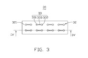
- FIG. 4 is a schematic, cross-sectional view of the adhesive layer in FIG. 3 as viewed along line IV-IV.
- FIG. 5 is a schematic view of a printed circuit board according to a third embodiment.
- FIG. 6 is a schematic view of another printed circuit board according to a fourth embodiment.
- FIG. 7 is a schematic, cross-sectional view of a folded flexible printed circuit board with a first portion and a second portion jointed together via a double-sided adhesive layer.
- FIG. 9 is similar to FIG. 7 , but shows the second portion of the folded flexible printed circuit board peeling-off from the double-sided adhesive layer.
- the adhesive main body 22 can defines only one through-hole 23 .
- the only one through-hole 23 should have a large size so that the inner adhesive 24 filled into the through-hole 23 can have large adhesive areas exposed from the first adhesive surface 221 and the second adhesive surface 222 simultaneously.
- Such enough adhesive areas can reinforce the first adhesive surface 211 and the second adhesive surface 222 adhering to other elements (e.g., printed circuit boards) tightly.
- adhesiveness of the first adhesive surface 211 and the second adhesive surface 222 of the adhesive main body 22 can be improved effectively.
- the printed circuit board assembly 40 is a bended structure.
- the printed circuit board assembly 40 includes a first portion 41 , a bending portion 42 , a second portion 43 and the adhesive layer 20 between the first portion 41 and the second portion 43 .
- the printed circuit board assembly 40 is bent into a U-shaped figuration with the second portion 43 overlapping the first portion 41 via bending of the bending portion 42 .
- the first portion 41 and the second portion 43 can each be either a rigid portion such as a rigid printed circuit board or a flexible portion such as a portion of a flexible printed circuit board.
- the first portion 41 , the bending portion 42 and the second portion 43 are all portions of a flexible printed circuit board.
- the printed circuit board assembly 40 also can use the adhesive layer 30 of the second embodiment.
- the printed circuit board assembly 50 can be described as a general multilayer printed circuit board.
- the printed circuit board assembly 50 does not include the bending portion 52 , the first portion 51 , the stiffener 54 and the second portion 53 adhered together via the first adhesive layer 201 and the second adhesive layer 202 can collectively be a strengthened double-layer printed circuit board.
Abstract
Description
Claims (20)
Applications Claiming Priority (3)
| Application Number | Priority Date | Filing Date | Title |
|---|---|---|---|
| CN200710075613.1 | 2007-08-03 | ||
| CN2007100756131A CN101360386B (en) | 2007-08-03 | 2007-08-03 | Circuit board binding glue layer and circuit board comprising the glue layer |
| CN200710075613 | 2007-08-03 |
Publications (2)
| Publication Number | Publication Date |
|---|---|
| US20090035566A1 US20090035566A1 (en) | 2009-02-05 |
| US7728232B2 true US7728232B2 (en) | 2010-06-01 |
Family
ID=40332698
Family Applications (1)
| Application Number | Title | Priority Date | Filing Date |
|---|---|---|---|
| US11/964,578 Expired - Fee Related US7728232B2 (en) | 2007-08-03 | 2007-12-26 | Printed circuit board assembly having adhesive layer |
Country Status (2)
| Country | Link |
|---|---|
| US (1) | US7728232B2 (en) |
| CN (1) | CN101360386B (en) |
Cited By (3)
| Publication number | Priority date | Publication date | Assignee | Title |
|---|---|---|---|---|
| US20120021621A1 (en) * | 2010-07-26 | 2012-01-26 | Kanghee Kim | Method for manufacturing multilayered flexible circuit board |
| US20160057897A1 (en) * | 2014-08-22 | 2016-02-25 | Apple Inc. | Shielding Can With Internal Magnetic Shielding Layer |
| US20170325356A1 (en) * | 2016-05-09 | 2017-11-09 | Fukui Precision Component (Shenzhen) Co., Ltd. | Ultrathin heat dissipation structure and a method for manufacturing same |
Families Citing this family (12)
| Publication number | Priority date | Publication date | Assignee | Title |
|---|---|---|---|---|
| US9050784B2 (en) | 2010-12-22 | 2015-06-09 | E I Du Pont De Nemours And Company | Fire resistant back-sheet for photovoltaic module |
| CN103076843A (en) * | 2011-10-26 | 2013-05-01 | 富泰华工业(深圳)有限公司 | Bonding structure and electronic device using same |
| CN102802366B (en) * | 2012-08-09 | 2015-07-29 | 皆利士多层线路版(中山)有限公司 | Printed substrate except gluing method |
| CN107393663B (en) * | 2013-07-11 | 2019-08-06 | 墙煌新材料股份有限公司 | Electronic component combination |
| CN105580150B (en) | 2013-09-25 | 2018-12-25 | 琳得科株式会社 | Thermal conductivity adhesive sheet, its manufacturing method and the electronic device using the thermal conductivity adhesive sheet |
| CN104881629B (en) * | 2015-03-31 | 2019-05-17 | 业成科技(成都)有限公司 | Fingerprint identification device |
| CN104869749B (en) * | 2015-04-17 | 2018-02-27 | 麦克思股份有限公司 | Electronic installation |
| CN105702170A (en) | 2016-04-05 | 2016-06-22 | 京东方科技集团股份有限公司 | Adhesive material, flexible module, display equipment and manufacturing method of flexible module |
| CN108260280B (en) * | 2017-12-04 | 2020-12-01 | 深圳市新宇腾跃电子有限公司 | FPC bending forming process |
| CN109382960A (en) * | 2018-11-29 | 2019-02-26 | 江苏力奥智能装备有限公司 | A kind of equipment and its processing method producing plastic handles band |
| CN110810937A (en) * | 2019-12-07 | 2020-02-21 | 成文文 | Non-sewing hot-melt garment and preparation method and application thereof |
| CN111915990A (en) * | 2020-08-07 | 2020-11-10 | 武汉华星光电半导体显示技术有限公司 | Display panel and display device |
Citations (6)
| Publication number | Priority date | Publication date | Assignee | Title |
|---|---|---|---|---|
| US4209481A (en) * | 1976-04-19 | 1980-06-24 | Toray Industries, Inc. | Process for producing an anisotropically electroconductive sheet |
| US5275856A (en) * | 1991-11-12 | 1994-01-04 | Minnesota Mining And Manufacturing Company | Electrically conductive adhesive web |
| US5751068A (en) * | 1994-09-01 | 1998-05-12 | Intel Corporation | Tape with solder forms for semiconductor devices |
| US6093476A (en) * | 1997-05-02 | 2000-07-25 | Shinko Electric Industries Co., Ltd. | Wiring substrate having vias |
| US6854985B1 (en) * | 1998-12-16 | 2005-02-15 | Paricon Technologies Corporation | Elastomeric interconnection device and methods for making same |
| US6908318B2 (en) * | 2001-08-08 | 2005-06-21 | 3M Innovative Properties Company | Batch electrically connecting sheet |
Family Cites Families (3)
| Publication number | Priority date | Publication date | Assignee | Title |
|---|---|---|---|---|
| EP0999589B2 (en) * | 1995-03-20 | 2013-11-13 | Kabushiki Kaisha Toshiba | Silicon nitride circuit board |
| DE10361450A1 (en) * | 2003-12-23 | 2005-07-28 | EMUGE-Werk Richard Glimpel GmbH & Co. KG Fabrik für Präzisionswerkzeuge | Cutting element and tool with at least one cutting element |
| US7040844B1 (en) * | 2005-03-08 | 2006-05-09 | Mitsubishi Materials Corporation | Throwaway insert and throwaway-type rotary cutting tool |
-
2007
- 2007-08-03 CN CN2007100756131A patent/CN101360386B/en not_active Expired - Fee Related
- 2007-12-26 US US11/964,578 patent/US7728232B2/en not_active Expired - Fee Related
Patent Citations (6)
| Publication number | Priority date | Publication date | Assignee | Title |
|---|---|---|---|---|
| US4209481A (en) * | 1976-04-19 | 1980-06-24 | Toray Industries, Inc. | Process for producing an anisotropically electroconductive sheet |
| US5275856A (en) * | 1991-11-12 | 1994-01-04 | Minnesota Mining And Manufacturing Company | Electrically conductive adhesive web |
| US5751068A (en) * | 1994-09-01 | 1998-05-12 | Intel Corporation | Tape with solder forms for semiconductor devices |
| US6093476A (en) * | 1997-05-02 | 2000-07-25 | Shinko Electric Industries Co., Ltd. | Wiring substrate having vias |
| US6854985B1 (en) * | 1998-12-16 | 2005-02-15 | Paricon Technologies Corporation | Elastomeric interconnection device and methods for making same |
| US6908318B2 (en) * | 2001-08-08 | 2005-06-21 | 3M Innovative Properties Company | Batch electrically connecting sheet |
Cited By (5)
| Publication number | Priority date | Publication date | Assignee | Title |
|---|---|---|---|---|
| US20120021621A1 (en) * | 2010-07-26 | 2012-01-26 | Kanghee Kim | Method for manufacturing multilayered flexible circuit board |
| US8530747B2 (en) * | 2010-07-26 | 2013-09-10 | Lg Electronics Inc. | Method for manufacturing multilayered flexible circuit board |
| US20160057897A1 (en) * | 2014-08-22 | 2016-02-25 | Apple Inc. | Shielding Can With Internal Magnetic Shielding Layer |
| US20170325356A1 (en) * | 2016-05-09 | 2017-11-09 | Fukui Precision Component (Shenzhen) Co., Ltd. | Ultrathin heat dissipation structure and a method for manufacturing same |
| US10448540B2 (en) * | 2016-05-09 | 2019-10-15 | Avary Holding (Shenzhen) Co., Limited. | Ultrathin heat dissipation structure |
Also Published As
| Publication number | Publication date |
|---|---|
| US20090035566A1 (en) | 2009-02-05 |
| CN101360386B (en) | 2010-10-06 |
| CN101360386A (en) | 2009-02-04 |
Similar Documents
| Publication | Publication Date | Title |
|---|---|---|
| US7728232B2 (en) | Printed circuit board assembly having adhesive layer | |
| US6458234B1 (en) | Methods of fixturing a flexible substrate and a processing carrier and methods of processing a flexible substrate | |
| US9743533B2 (en) | Method for manufacturing rigid-flexible printed circuit board | |
| US20130161078A1 (en) | Rigid-flex circuit board and manufacturing method | |
| JPH057057A (en) | Flexible wiring board | |
| JPH05243693A (en) | Printed circuit having break resistance and printed circuit board and compact personal computer having the same printed circuit board | |
| US5889321A (en) | Stiffeners with improved adhesion to flexible substrates | |
| US10219379B1 (en) | Stacked flexible printed circuit board assembly with side connection section | |
| JPH06120643A (en) | Flexible wiring board and production thereof | |
| TWM502303U (en) | Printed circuit board | |
| US5583320A (en) | Reinforcement for flexible printed circuit board and reinforced flexible printed circuit board | |
| CN113242643A (en) | Circuit board and display device | |
| CN109714883B (en) | Circuit compensation FPC | |
| US20090176080A1 (en) | Stiffener and strengthened flexible printed circuit board having the same | |
| JP2001036246A (en) | Wiring board and multilayer wiring board using the same | |
| JP5489013B2 (en) | Flexible printed circuit board | |
| US7992290B2 (en) | Method of making a flexible printed circuit board | |
| JP3176858B2 (en) | Double-sided copper-clad printed wiring board | |
| CN112911792B (en) | FPC assembly and surface mounting method | |
| JP2009188326A (en) | Flexible wiring board | |
| JP5027535B2 (en) | Multilayer printed wiring board and manufacturing method thereof | |
| JPH07111371A (en) | Flexible printed board | |
| JP4692815B2 (en) | Flexible printed circuit board | |
| JP2006041044A (en) | Multilayer flexible wiring circuit board | |
| CN215011177U (en) | Foldable flexible circuit board structure |
Legal Events
| Date | Code | Title | Description |
|---|---|---|---|
| AS | Assignment |
Owner name: FUKUI PRECISION COMPONENT (SHENZHEN) CO., LTD., CH Free format text: ASSIGNMENT OF ASSIGNORS INTEREST;ASSIGNORS:HUANG, FENG-YAN;LIOU, SHING-TZA;REEL/FRAME:020290/0631 Effective date: 20071221 Owner name: FOXCONN ADVANCED TECHNOLOGY INC., TAIWAN Free format text: ASSIGNMENT OF ASSIGNORS INTEREST;ASSIGNORS:HUANG, FENG-YAN;LIOU, SHING-TZA;REEL/FRAME:020290/0631 Effective date: 20071221 Owner name: FUKUI PRECISION COMPONENT (SHENZHEN) CO., LTD.,CHI Free format text: ASSIGNMENT OF ASSIGNORS INTEREST;ASSIGNORS:HUANG, FENG-YAN;LIOU, SHING-TZA;REEL/FRAME:020290/0631 Effective date: 20071221 Owner name: FOXCONN ADVANCED TECHNOLOGY INC.,TAIWAN Free format text: ASSIGNMENT OF ASSIGNORS INTEREST;ASSIGNORS:HUANG, FENG-YAN;LIOU, SHING-TZA;REEL/FRAME:020290/0631 Effective date: 20071221 |
|
| STCF | Information on status: patent grant |
Free format text: PATENTED CASE |
|
| AS | Assignment |
Owner name: ZHEN DING TECHNOLOGY CO., LTD., TAIWAN Free format text: CHANGE OF NAME;ASSIGNOR:FOXCONN ADVANCED TECHNOLOGY INC.;REEL/FRAME:026894/0412 Effective date: 20110613 |
|
| FPAY | Fee payment |
Year of fee payment: 4 |
|
| AS | Assignment |
Owner name: GARUDA TECHNOLOGY CO., LTD, TAIWAN Free format text: ASSIGNMENT OF ASSIGNORS INTEREST;ASSIGNORS:FUKUI PRECISION COMPONENT (SHENZHEN) CO., LTD.;ZHEN DING TECHNOLOGY CO., LTD.;REEL/FRAME:040979/0020 Effective date: 20170101 Owner name: FUKUI PRECISION COMPONENT (SHENZHEN) CO., LTD., CH Free format text: ASSIGNMENT OF ASSIGNORS INTEREST;ASSIGNORS:FUKUI PRECISION COMPONENT (SHENZHEN) CO., LTD.;ZHEN DING TECHNOLOGY CO., LTD.;REEL/FRAME:040979/0020 Effective date: 20170101 |
|
| AS | Assignment |
Owner name: AVARY HOLDING (SHENZHEN) CO., LIMITED., CHINA Free format text: CHANGE OF NAME;ASSIGNOR:FUKUI PRECISION COMPONENT (SHENZHEN) CO., LTD.;REEL/FRAME:043312/0761 Effective date: 20170524 |
|
| AS | Assignment |
Owner name: AVARY HOLDING (SHENZHEN) CO., LIMITED., CHINA Free format text: CHANGE OF NAME;ASSIGNOR:FUKUI PRECISION COMPONENT (SHENZHEN) CO., LTD.;REEL/FRAME:043378/0038 Effective date: 20170524 |
|
| MAFP | Maintenance fee payment |
Free format text: PAYMENT OF MAINTENANCE FEE, 8TH YEAR, LARGE ENTITY (ORIGINAL EVENT CODE: M1552) Year of fee payment: 8 |
|
| FEPP | Fee payment procedure |
Free format text: MAINTENANCE FEE REMINDER MAILED (ORIGINAL EVENT CODE: REM.); ENTITY STATUS OF PATENT OWNER: LARGE ENTITY |
|
| LAPS | Lapse for failure to pay maintenance fees |
Free format text: PATENT EXPIRED FOR FAILURE TO PAY MAINTENANCE FEES (ORIGINAL EVENT CODE: EXP.); ENTITY STATUS OF PATENT OWNER: LARGE ENTITY |
|
| STCH | Information on status: patent discontinuation |
Free format text: PATENT EXPIRED DUE TO NONPAYMENT OF MAINTENANCE FEES UNDER 37 CFR 1.362 |
|
| FP | Lapsed due to failure to pay maintenance fee |
Effective date: 20220601 |