US7679148B2 - Semiconductor device, production method and production device thereof - Google Patents
Semiconductor device, production method and production device thereof Download PDFInfo
- Publication number
- US7679148B2 US7679148B2 US10/521,311 US52131105A US7679148B2 US 7679148 B2 US7679148 B2 US 7679148B2 US 52131105 A US52131105 A US 52131105A US 7679148 B2 US7679148 B2 US 7679148B2
- Authority
- US
- United States
- Prior art keywords
- metal
- silicon oxide
- region
- film
- silicate
- Prior art date
- Legal status (The legal status is an assumption and is not a legal conclusion. Google has not performed a legal analysis and makes no representation as to the accuracy of the status listed.)
- Expired - Fee Related, expires
Links
- 239000004065 semiconductor Substances 0.000 title claims abstract description 26
- 238000004519 manufacturing process Methods 0.000 title abstract description 39
- 229910052751 metal Inorganic materials 0.000 claims abstract description 247
- VYPSYNLAJGMNEJ-UHFFFAOYSA-N Silicium dioxide Chemical compound O=[Si]=O VYPSYNLAJGMNEJ-UHFFFAOYSA-N 0.000 claims abstract description 196
- 229910052814 silicon oxide Inorganic materials 0.000 claims abstract description 194
- 239000002184 metal Substances 0.000 claims abstract description 184
- XUIMIQQOPSSXEZ-UHFFFAOYSA-N Silicon Chemical compound [Si] XUIMIQQOPSSXEZ-UHFFFAOYSA-N 0.000 claims abstract description 151
- 229910052710 silicon Inorganic materials 0.000 claims abstract description 150
- 239000010703 silicon Substances 0.000 claims abstract description 150
- BPQQTUXANYXVAA-UHFFFAOYSA-N Orthosilicate Chemical group [O-][Si]([O-])([O-])[O-] BPQQTUXANYXVAA-UHFFFAOYSA-N 0.000 claims abstract description 127
- 239000000203 mixture Substances 0.000 claims abstract description 37
- 230000007423 decrease Effects 0.000 claims description 11
- 239000010408 film Substances 0.000 abstract description 415
- 239000000758 substrate Substances 0.000 abstract description 102
- 238000000034 method Methods 0.000 abstract description 68
- 238000010438 heat treatment Methods 0.000 abstract description 59
- 239000010409 thin film Substances 0.000 abstract description 55
- 230000008569 process Effects 0.000 abstract description 51
- 230000015572 biosynthetic process Effects 0.000 abstract description 12
- 238000005137 deposition process Methods 0.000 abstract description 6
- IJGRMHOSHXDMSA-UHFFFAOYSA-N Atomic nitrogen Chemical compound N#N IJGRMHOSHXDMSA-UHFFFAOYSA-N 0.000 description 50
- 238000000151 deposition Methods 0.000 description 49
- 230000008021 deposition Effects 0.000 description 38
- 238000006243 chemical reaction Methods 0.000 description 36
- QVGXLLKOCUKJST-UHFFFAOYSA-N atomic oxygen Chemical compound [O] QVGXLLKOCUKJST-UHFFFAOYSA-N 0.000 description 32
- 239000001301 oxygen Substances 0.000 description 32
- 229910052760 oxygen Inorganic materials 0.000 description 32
- 238000009792 diffusion process Methods 0.000 description 30
- 229910052757 nitrogen Inorganic materials 0.000 description 25
- 229910052746 lanthanum Inorganic materials 0.000 description 24
- FZLIPJUXYLNCLC-UHFFFAOYSA-N lanthanum atom Chemical compound [La] FZLIPJUXYLNCLC-UHFFFAOYSA-N 0.000 description 21
- 229910052735 hafnium Inorganic materials 0.000 description 19
- 239000012298 atmosphere Substances 0.000 description 15
- 238000007254 oxidation reaction Methods 0.000 description 15
- VBJZVLUMGGDVMO-UHFFFAOYSA-N hafnium atom Chemical compound [Hf] VBJZVLUMGGDVMO-UHFFFAOYSA-N 0.000 description 14
- 230000003647 oxidation Effects 0.000 description 14
- QGZKDVFQNNGYKY-UHFFFAOYSA-N Ammonia Chemical compound N QGZKDVFQNNGYKY-UHFFFAOYSA-N 0.000 description 13
- 206010021143 Hypoxia Diseases 0.000 description 13
- 150000004767 nitrides Chemical class 0.000 description 13
- 238000010586 diagram Methods 0.000 description 12
- 238000005755 formation reaction Methods 0.000 description 12
- 239000000463 material Substances 0.000 description 12
- 229910044991 metal oxide Inorganic materials 0.000 description 12
- 230000000694 effects Effects 0.000 description 11
- 150000004706 metal oxides Chemical class 0.000 description 11
- 230000007547 defect Effects 0.000 description 10
- 238000009826 distribution Methods 0.000 description 10
- 238000004544 sputter deposition Methods 0.000 description 10
- 238000001704 evaporation Methods 0.000 description 9
- 229910052914 metal silicate Inorganic materials 0.000 description 8
- 238000001465 metallisation Methods 0.000 description 8
- 229910052581 Si3N4 Inorganic materials 0.000 description 7
- 229910021529 ammonia Inorganic materials 0.000 description 7
- 230000008020 evaporation Effects 0.000 description 7
- 239000007789 gas Substances 0.000 description 7
- 230000006872 improvement Effects 0.000 description 7
- 230000007246 mechanism Effects 0.000 description 7
- HQVNEWCFYHHQES-UHFFFAOYSA-N silicon nitride Chemical compound N12[Si]34N5[Si]62N3[Si]51N64 HQVNEWCFYHHQES-UHFFFAOYSA-N 0.000 description 7
- KRHYYFGTRYWZRS-UHFFFAOYSA-N Fluorane Chemical compound F KRHYYFGTRYWZRS-UHFFFAOYSA-N 0.000 description 6
- UFHFLCQGNIYNRP-UHFFFAOYSA-N Hydrogen Chemical compound [H][H] UFHFLCQGNIYNRP-UHFFFAOYSA-N 0.000 description 6
- MCMNRKCIXSYSNV-UHFFFAOYSA-N Zirconium dioxide Chemical compound O=[Zr]=O MCMNRKCIXSYSNV-UHFFFAOYSA-N 0.000 description 6
- 238000005229 chemical vapour deposition Methods 0.000 description 6
- 230000006866 deterioration Effects 0.000 description 6
- 239000001257 hydrogen Substances 0.000 description 5
- 229910052739 hydrogen Inorganic materials 0.000 description 5
- XKRFYHLGVUSROY-UHFFFAOYSA-N Argon Chemical compound [Ar] XKRFYHLGVUSROY-UHFFFAOYSA-N 0.000 description 4
- 238000005516 engineering process Methods 0.000 description 4
- CJNBYAVZURUTKZ-UHFFFAOYSA-N hafnium(IV) oxide Inorganic materials O=[Hf]=O CJNBYAVZURUTKZ-UHFFFAOYSA-N 0.000 description 4
- 238000001883 metal evaporation Methods 0.000 description 4
- 238000002407 reforming Methods 0.000 description 4
- 230000005641 tunneling Effects 0.000 description 4
- 229910052726 zirconium Inorganic materials 0.000 description 4
- 229910052684 Cerium Inorganic materials 0.000 description 3
- 229910052692 Dysprosium Inorganic materials 0.000 description 3
- 229910052691 Erbium Inorganic materials 0.000 description 3
- 229910052693 Europium Inorganic materials 0.000 description 3
- 229910052688 Gadolinium Inorganic materials 0.000 description 3
- 229910052689 Holmium Inorganic materials 0.000 description 3
- 229910052765 Lutetium Inorganic materials 0.000 description 3
- 229910052779 Neodymium Inorganic materials 0.000 description 3
- 229910052777 Praseodymium Inorganic materials 0.000 description 3
- 229910052772 Samarium Inorganic materials 0.000 description 3
- 229910052771 Terbium Inorganic materials 0.000 description 3
- 229910052775 Thulium Inorganic materials 0.000 description 3
- 229910052769 Ytterbium Inorganic materials 0.000 description 3
- 229910052782 aluminium Inorganic materials 0.000 description 3
- -1 ammonia peroxide Chemical class 0.000 description 3
- 238000000277 atomic layer chemical vapour deposition Methods 0.000 description 3
- 238000013461 design Methods 0.000 description 3
- 238000011161 development Methods 0.000 description 3
- 229910052758 niobium Inorganic materials 0.000 description 3
- 229910052761 rare earth metal Inorganic materials 0.000 description 3
- 238000005546 reactive sputtering Methods 0.000 description 3
- 230000009467 reduction Effects 0.000 description 3
- 229910052706 scandium Inorganic materials 0.000 description 3
- 229910052715 tantalum Inorganic materials 0.000 description 3
- 229910052719 titanium Inorganic materials 0.000 description 3
- 229910052727 yttrium Inorganic materials 0.000 description 3
- 229910018557 Si O Inorganic materials 0.000 description 2
- 238000010306 acid treatment Methods 0.000 description 2
- 229910052786 argon Inorganic materials 0.000 description 2
- 238000004140 cleaning Methods 0.000 description 2
- 238000002425 crystallisation Methods 0.000 description 2
- 238000005566 electron beam evaporation Methods 0.000 description 2
- 238000010894 electron beam technology Methods 0.000 description 2
- 238000005530 etching Methods 0.000 description 2
- 238000011156 evaluation Methods 0.000 description 2
- 230000005669 field effect Effects 0.000 description 2
- 238000003780 insertion Methods 0.000 description 2
- 230000037431 insertion Effects 0.000 description 2
- 239000011810 insulating material Substances 0.000 description 2
- 229910052747 lanthanoid Inorganic materials 0.000 description 2
- 150000002602 lanthanoids Chemical class 0.000 description 2
- 238000005121 nitriding Methods 0.000 description 2
- 239000012299 nitrogen atmosphere Substances 0.000 description 2
- 125000004430 oxygen atom Chemical group O* 0.000 description 2
- 238000009832 plasma treatment Methods 0.000 description 2
- 229910021420 polycrystalline silicon Inorganic materials 0.000 description 2
- 229920005591 polysilicon Polymers 0.000 description 2
- 239000010453 quartz Substances 0.000 description 2
- 238000004335 scaling law Methods 0.000 description 2
- LIVNPJMFVYWSIS-UHFFFAOYSA-N silicon monoxide Inorganic materials [Si-]#[O+] LIVNPJMFVYWSIS-UHFFFAOYSA-N 0.000 description 2
- 238000001179 sorption measurement Methods 0.000 description 2
- 239000000126 substance Substances 0.000 description 2
- 238000006467 substitution reaction Methods 0.000 description 2
- 238000001771 vacuum deposition Methods 0.000 description 2
- 238000007738 vacuum evaporation Methods 0.000 description 2
- 238000004833 X-ray photoelectron spectroscopy Methods 0.000 description 1
- 150000004645 aluminates Chemical class 0.000 description 1
- PNEYBMLMFCGWSK-UHFFFAOYSA-N aluminium oxide Inorganic materials [O-2].[O-2].[O-2].[Al+3].[Al+3] PNEYBMLMFCGWSK-UHFFFAOYSA-N 0.000 description 1
- 125000004429 atom Chemical group 0.000 description 1
- 230000004888 barrier function Effects 0.000 description 1
- 238000004364 calculation method Methods 0.000 description 1
- 239000002131 composite material Substances 0.000 description 1
- 239000000470 constituent Substances 0.000 description 1
- 229910052593 corundum Inorganic materials 0.000 description 1
- 230000008025 crystallization Effects 0.000 description 1
- 230000001419 dependent effect Effects 0.000 description 1
- 238000010292 electrical insulation Methods 0.000 description 1
- 230000002349 favourable effect Effects 0.000 description 1
- 239000012212 insulator Substances 0.000 description 1
- 150000002500 ions Chemical class 0.000 description 1
- MRELNEQAGSRDBK-UHFFFAOYSA-N lanthanum oxide Inorganic materials [O-2].[O-2].[O-2].[La+3].[La+3] MRELNEQAGSRDBK-UHFFFAOYSA-N 0.000 description 1
- 239000007769 metal material Substances 0.000 description 1
- QJGQUHMNIGDVPM-UHFFFAOYSA-N nitrogen(.) Chemical compound [N] QJGQUHMNIGDVPM-UHFFFAOYSA-N 0.000 description 1
- 238000005457 optimization Methods 0.000 description 1
- 239000007800 oxidant agent Substances 0.000 description 1
- KTUFCUMIWABKDW-UHFFFAOYSA-N oxo(oxolanthaniooxy)lanthanum Chemical compound O=[La]O[La]=O KTUFCUMIWABKDW-UHFFFAOYSA-N 0.000 description 1
- 230000002265 prevention Effects 0.000 description 1
- 238000012545 processing Methods 0.000 description 1
- 230000001737 promoting effect Effects 0.000 description 1
- 238000012827 research and development Methods 0.000 description 1
- 238000005204 segregation Methods 0.000 description 1
- 150000004760 silicates Chemical class 0.000 description 1
- 230000007847 structural defect Effects 0.000 description 1
- 238000007736 thin film deposition technique Methods 0.000 description 1
- 238000000427 thin-film deposition Methods 0.000 description 1
- 238000001039 wet etching Methods 0.000 description 1
- 229910001845 yogo sapphire Inorganic materials 0.000 description 1
Images


Classifications
-
- H—ELECTRICITY
- H01—ELECTRIC ELEMENTS
- H01L—SEMICONDUCTOR DEVICES NOT COVERED BY CLASS H10
- H01L21/00—Processes or apparatus adapted for the manufacture or treatment of semiconductor or solid state devices or of parts thereof
- H01L21/02—Manufacture or treatment of semiconductor devices or of parts thereof
- H01L21/04—Manufacture or treatment of semiconductor devices or of parts thereof the devices having at least one potential-jump barrier or surface barrier, e.g. PN junction, depletion layer or carrier concentration layer
- H01L21/18—Manufacture or treatment of semiconductor devices or of parts thereof the devices having at least one potential-jump barrier or surface barrier, e.g. PN junction, depletion layer or carrier concentration layer the devices having semiconductor bodies comprising elements of Group IV of the Periodic System or AIIIBV compounds with or without impurities, e.g. doping materials
- H01L21/28—Manufacture of electrodes on semiconductor bodies using processes or apparatus not provided for in groups H01L21/20 - H01L21/268
- H01L21/28008—Making conductor-insulator-semiconductor electrodes
- H01L21/28017—Making conductor-insulator-semiconductor electrodes the insulator being formed after the semiconductor body, the semiconductor being silicon
- H01L21/28158—Making the insulator
- H01L21/28167—Making the insulator on single crystalline silicon, e.g. using a liquid, i.e. chemical oxidation
- H01L21/28202—Making the insulator on single crystalline silicon, e.g. using a liquid, i.e. chemical oxidation in a nitrogen-containing ambient, e.g. nitride deposition, growth, oxynitridation, NH3 nitridation, N2O oxidation, thermal nitridation, RTN, plasma nitridation, RPN
-
- H—ELECTRICITY
- H01—ELECTRIC ELEMENTS
- H01L—SEMICONDUCTOR DEVICES NOT COVERED BY CLASS H10
- H01L21/00—Processes or apparatus adapted for the manufacture or treatment of semiconductor or solid state devices or of parts thereof
- H01L21/02—Manufacture or treatment of semiconductor devices or of parts thereof
- H01L21/04—Manufacture or treatment of semiconductor devices or of parts thereof the devices having at least one potential-jump barrier or surface barrier, e.g. PN junction, depletion layer or carrier concentration layer
- H01L21/18—Manufacture or treatment of semiconductor devices or of parts thereof the devices having at least one potential-jump barrier or surface barrier, e.g. PN junction, depletion layer or carrier concentration layer the devices having semiconductor bodies comprising elements of Group IV of the Periodic System or AIIIBV compounds with or without impurities, e.g. doping materials
- H01L21/28—Manufacture of electrodes on semiconductor bodies using processes or apparatus not provided for in groups H01L21/20 - H01L21/268
- H01L21/28008—Making conductor-insulator-semiconductor electrodes
- H01L21/28017—Making conductor-insulator-semiconductor electrodes the insulator being formed after the semiconductor body, the semiconductor being silicon
- H01L21/28026—Making conductor-insulator-semiconductor electrodes the insulator being formed after the semiconductor body, the semiconductor being silicon characterised by the conductor
- H01L21/28035—Making conductor-insulator-semiconductor electrodes the insulator being formed after the semiconductor body, the semiconductor being silicon characterised by the conductor the final conductor layer next to the insulator being silicon, e.g. polysilicon, with or without impurities
-
- H—ELECTRICITY
- H01—ELECTRIC ELEMENTS
- H01L—SEMICONDUCTOR DEVICES NOT COVERED BY CLASS H10
- H01L29/00—Semiconductor devices adapted for rectifying, amplifying, oscillating or switching, or capacitors or resistors with at least one potential-jump barrier or surface barrier, e.g. PN junction depletion layer or carrier concentration layer; Details of semiconductor bodies or of electrodes thereof ; Multistep manufacturing processes therefor
- H01L29/40—Electrodes ; Multistep manufacturing processes therefor
- H01L29/43—Electrodes ; Multistep manufacturing processes therefor characterised by the materials of which they are formed
- H01L29/49—Metal-insulator-semiconductor electrodes, e.g. gates of MOSFET
- H01L29/51—Insulating materials associated therewith
- H01L29/511—Insulating materials associated therewith with a compositional variation, e.g. multilayer structures
- H01L29/513—Insulating materials associated therewith with a compositional variation, e.g. multilayer structures the variation being perpendicular to the channel plane
-
- H—ELECTRICITY
- H01—ELECTRIC ELEMENTS
- H01L—SEMICONDUCTOR DEVICES NOT COVERED BY CLASS H10
- H01L29/00—Semiconductor devices adapted for rectifying, amplifying, oscillating or switching, or capacitors or resistors with at least one potential-jump barrier or surface barrier, e.g. PN junction depletion layer or carrier concentration layer; Details of semiconductor bodies or of electrodes thereof ; Multistep manufacturing processes therefor
- H01L29/40—Electrodes ; Multistep manufacturing processes therefor
- H01L29/43—Electrodes ; Multistep manufacturing processes therefor characterised by the materials of which they are formed
- H01L29/49—Metal-insulator-semiconductor electrodes, e.g. gates of MOSFET
- H01L29/51—Insulating materials associated therewith
- H01L29/518—Insulating materials associated therewith the insulating material containing nitrogen, e.g. nitride, oxynitride, nitrogen-doped material
-
- H—ELECTRICITY
- H01—ELECTRIC ELEMENTS
- H01L—SEMICONDUCTOR DEVICES NOT COVERED BY CLASS H10
- H01L29/00—Semiconductor devices adapted for rectifying, amplifying, oscillating or switching, or capacitors or resistors with at least one potential-jump barrier or surface barrier, e.g. PN junction depletion layer or carrier concentration layer; Details of semiconductor bodies or of electrodes thereof ; Multistep manufacturing processes therefor
- H01L29/66—Types of semiconductor device ; Multistep manufacturing processes therefor
- H01L29/66007—Multistep manufacturing processes
- H01L29/66075—Multistep manufacturing processes of devices having semiconductor bodies comprising group 14 or group 13/15 materials
- H01L29/66227—Multistep manufacturing processes of devices having semiconductor bodies comprising group 14 or group 13/15 materials the devices being controllable only by the electric current supplied or the electric potential applied, to an electrode which does not carry the current to be rectified, amplified or switched, e.g. three-terminal devices
- H01L29/66409—Unipolar field-effect transistors
- H01L29/66477—Unipolar field-effect transistors with an insulated gate, i.e. MISFET
- H01L29/6656—Unipolar field-effect transistors with an insulated gate, i.e. MISFET using multiple spacer layers, e.g. multiple sidewall spacers
Definitions
- the present invention relates to a semiconductor device having a high dielectric constant thin film, and manufacturing method and manufacturing apparatus thereof, more particularly, to a semiconductor device which provides higher performance and lower power consumption of a gate insulating film which constitutes an MOSFET (Metal-Oxide-Semiconductor Field Effect Transistor), and manufacturing method and manufacturing apparatus thereof.
- MOSFET Metal-Oxide-Semiconductor Field Effect Transistor
- Silicon oxide films have process stability and excellent electrical insulation, and are being used for gate insulating materials of an MOSFET.
- thinning of a gate insulating film has been increasingly growing, and a device with a gate length of 100 nm or less requires a thickness of a silicon oxide film which is the gate insulating film, to be 1.5 nm or less from a requirement of the scaling law.
- the magnitude of tunneling current sandwiched between a gate insulating layer and the gate electrode becomes an unignorable value against source/drain current, and exceeds a permissible range of device design. This would be a big barrier to promoting higher performance and lower power consumption of the MOSFET. Accordingly, research and development is proceeding with the aim to thin a film thickness of an effective gate insulating film and to control the tunneling current to within the permissible values.
- One of them is a method of adding nitrogen into a silicon oxide film to thereby increase dielectric constant more than that of a pure silicon oxide film, and to reduce a film thickness of an effective, namely, electrical gate insulating layer without thinning a physical film thickness.
- Fabricating techniques of such a silicon oxynitride film include a method of making high-temperature heat treatment of the silicon oxide film in gas containing nitrogen such as ammonia (NH 3 ) to thereby introduce the nitrogen into the silicon oxide film after forming the silicon oxide film on a surface of a silicon substrate.
- this method gives rise to a problem that the heat treatment in gas atmosphere causes segregation of the nitrogen into an interface between the silicon oxide film and the silicon substrate to produce deterioration of interface electrical characteristics.
- each of a metal oxide and a silicate thin film features the following. If the metal oxides such as ZrO 2 and HfO 2 are used as a high dielectric constant gate insulating film, higher relative dielectric constant may be achieved. On the other hand, it is believed that although the relative dielectric constant decreases in a silicate material in which silicon is contained, thermal stability is enhanced, as well as the interface electrical characteristics may be improved as compared with the case where the metal oxides are directly joined onto the silicon substrate.
- next-generation MOSFET is considering to adopt the high dielectric constant thin film as the gate insulating film materials, and to adopt CVD (Chemical Vapor Deposition) using different kinds of source gas, or ALD (Atomic Layer Chemical Vapor Deposition) which controls CVD deposition on an atomic layer basis, as deposition techniques of the high dielectric constant thin film onto the surface of the silicon substrate.
- CVD Chemical Vapor Deposition
- ALD Atomic Layer Chemical Vapor Deposition
- a physical evaporation method such as sputtering, reactive sputtering, or Molecular Beam Deposition has been used with the aim of material search.
- a high dielectric constant film has been directly deposited on a surface of a silicon substrate, and in which an ultra-thin silicon oxide film, to be more precise, with a thickness of normally less than 1 nm, has been inserted into an interface between a high dielectric constant thin film and the silicon substrate for the purpose of controlling an early reaction of CVD or ALD deposition, and of improving thermal stability of the interface between the high dielectric constant thin film and the silicon substrate.
- the ultra-thin silicon oxide film is formed on the surface of the silicon substrate, and then the deposition of the high dielectric constant thin film is carried out by different kinds of deposition methods.
- deposition techniques Commonalties in these deposition techniques are that stoichiometric composition on the surface of the silicon substrate, or the deposition of the high dielectric constant film in agreement with silicate composition which is neither too much nor too little in oxygen concentration is necessary, and in particular, a structural defect such as an oxygen deficiency in a film causes deterioration of electrical characteristics and increase in leakage current.
- the characteristics have been studied heretofore.
- the biggest technical problem toward the development of the next-generation MOSFET is improvement in the interface electrical characteristics between the high dielectric constant thin film and the silicon substrate. More specifically, the interface defect density between the high dielectric constant thin film interface and the silicon substrate is higher by one to two digits than the interface defect density between the silicon oxide film and the silicon substrate, deterioration of the mobility becomes significant due to charge captured by the interface defect, and current drive capability of the MOSFET declines. This cancels out the effect that the gate insulating film has been thinned.
- an interface structure which determines the electrical characteristics is deeply related to a fabrication method of the high dielectric constant thin film. For example, even if the high dielectric constant thin film is directly deposited on the surface of the silicon substrate by means of the CVD or sputtering method, oxidation of the silicon substrate progresses concurrently with thin film deposition to form an interface layer mainly comprising the silicon oxide film when an oxidizing agent is introduced during the deposition, or when a large amount of residual oxygen are present within deposition apparatus. It is difficult to independently control the deposition of these interface layers, thus it being impossible to independently design the structure in which the interface electrical characteristics are optimized.
- techniques in which a silicon oxide film is intentionally inserted as an interface oxide layer include a method of forming an ultra-thin silicon oxide film on a surface of a silicon substrate in advance before depositing a high dielectric constant thin film, and a method of depositing a high dielectric constant thin film before giving heat treatment to allow growth of the silicon oxide film.
- the former method has an effect that insertion of the silicon oxide film enhances interface thermal stability.
- a film thickness of the ultra-thin silicon oxide film which is formed on the surface of the silicon substrate should be 0.6 nm or less due to low relative dielectric constant of the silicon oxide film.
- an ultra-thin base silicon oxide film is sometimes altered in a process of depositing the high dielectric constant thin film on the ultra-thin silicon oxide film, and hence interface characteristics between the ultra-thin silicon oxide film and the silicon substrate deteriorate.
- the latter method is a method utilizing phenomenon in which oxygen easily diffuses in the high dielectric constant thin film to form an interface layer.
- metal elements in the high dielectric constant film diffuse into the interface layer in a heat treatment process, it is impossible to form an ideal interface between the silicon oxide film and the silicon substrate excellent in the electrical characteristics.
- the prior art had the problems that although in order to improve the interface electrical characteristics of the gate insulating film having high dielectric constant, formation of the high dielectric constant thin film excellent in film quality was necessary, while maintaining a good quality interface between the silicon oxide film and the silicon substrate, it was difficult to separate and control a forming process of the interface layer comprising the silicon oxide film, and a deposition process of the high dielectric constant film.
- a film thickness of said cap layer is 1 nm or less.
- the film thickness of said cap layer is 0.5 nm or less.
- said insulating film structure has the composition modulation in which the composition of silicon in a film thickness direction is high in the lowermost portion and uppermost portion and low in the central portion, in the vicinity of said silicon region.
- said insulating film structure has the composition modulation in which the composition of said at least one metal element in the film thickness direction is low in the lowermost portion and uppermost portion and high in the central portion, in the vicinity of said silicon region.
- Equivalent Oxide Thickness of said insulating film structure be smaller than the Equivalent Oxide Thickness of the silicon oxide film into which said at least one metal element is diffused.
- said silicon oxide constituting said at least one silicate region is a silicon oxynitride into which nitrogen has been introduced.
- the concentration distribution of said at least one metal element in said at least one silicate region is derived from the heat treatment under reduced pressure oxygen conditions below atmospheric pressure.
- said insulating film structure further includes a cap region composed of any one of the silicon nitride and the silicon oxynitride.
- a thickness of said cap region is 0.5 nm or less.
- said conductive region comprises the gate electrode
- said insulating film structure comprises the gate insulating film
- a hysteresis width of gate capacity-bias characteristics is 5 mV or less by an applied gate bias within device operating voltage
- said insulating film structure comprises said silicate region composed of the silicon oxide containing said at least one metal element, and the silicon oxide region composed of the silicon oxide not containing said at least one metal element, and that a physical thickness of said insulating film structure is 3.5 nm or less, the physical thickness of said silicate region being thinner than the physical thickness of said silicon oxide region.
- the physical thickness of said silicate region is 1.5 nm or less.
- said conductive region comprises the gate electrode
- said insulating film structure comprises the gate insulating film, the gate electrode having nitride film side walls.
- a second aspect of the present invention provides a manufacturing method of a semiconductor device including an insulating film structure which electrically insulates a conductive region from a silicon region, the manufacturing method at least comprising the steps of:
- said thermally diffused forms said insulating film structure including at least one silicon oxide region composed of the silicon oxide into which said at least one metal element is not diffused by said thermal diffusion, at least one metal rich region into which said at least one metal element has been diffused at high concentration, and said at least one silicate region which is located between said silicon oxide region and said metal rich region and into which said at least one metal element has been diffused at concentration lower than that of said metal rich region.
- said silicate region has composition modulation in which composition of said at least one metal element increases as closer to said metal rich region and decreases as closer to said silicon oxide region, and, on the other hand, in which the composition of silicon decreases as closer to said metal rich region and increases as closer to said silicon oxide region.
- said metal rich region comprises a metal oxide not containing silicon.
- said metal rich region comprises a metal rich silicate having higher concentration distribution of said at least one metal element than that of said silicate region.
- a process of forming said metal layer comprises a deposition process carried out by setting residual oxygen partial pressure to 1 ⁇ 10 ⁇ 6 T or less.
- the deposition process of said metal layer is carried out by causing temperature rise of said silicon region from room temperature.
- said nitride treatment process comprises the heat treatment in ammonia.
- said nitride treatment process comprises nitrogen plasma treatment.
- said at least one metal element is at least only any one of Zr, Hf, Ta, Al, Ti, Nb, Sc, Y, La, Ce, Pr, Nd, Sm, Eu, Gd, Tb, Dy, Ho, Er, Tm, Yb, and Lu.
- a source of the metal element comprises the metal layer abutting on a surface of the base silicon oxide film with a film thickness of not less than 0.6 nm, which extends on said silicon region.
- said at least one metal element contains at least only any one of Zr, Hf, Ta, Al, Ti, Nb, Sc, Y, La, Ce, Pr, Nd, Sm, Eu, Gd, Tb, Dy, Ho, Er, Tm, Yb, and Lu, and that the source of the metal element comprises the metal layer abutting on the surface of the base silicon oxide film with a film thickness of not less than 1 nm, which extends on said silicon region.
- a forming process of said metal layer is a process which is carried out on condition that the film thickness of metal deposition is 1 nm or less.
- the forming process of said metal layer is a process which is carried out on condition that the film thickness of the metal deposition is 0.6 nm or less.
- said heat treatment process is carried out for the silicate reaction in the interface between said metal layer and said base silicon oxide film to progress to an upper portion of said metal layer, thereby forming said insulating film structure up to and including the uppermost portion from silicate.
- the process of removing said reacted metal region is carried out by use of a hydrofluoric acid solution or an ammonia peroxide solution.
- said cap layer comprises any one of a silicon oxide film, a silicon oxynitride film, a silicon nitride film, and at least two laminated structures of these.
- the film thickness of said cap layer is 1 nm or less.
- the film thickness of said cap layer is 0.5 nm or less.
- said insulating film structure has the composition modulation in which the composition of silicon in the film thickness direction is high in the lowermost portion and uppermost portion and low in the central portion, in the vicinity of said silicon region.
- said insulating film structure has the composition modulation in which the composition of said at least one metal element in the film thickness direction is low in the lowermost portion and uppermost portion and high in the central portion, in the vicinity of said silicon region.
- said base silicon oxide film comprises a silicon oxynitride film into which nitrogen has been introduced.
- said silicon region comprises a silicon substrate
- said conductive region comprises a gate electrode
- said insulating film structure comprises a gate insulating film.
- a third aspect of the present invention provides manufacturing apparatus of a semiconductor device having a gate insulating film which electrically insulates a gate electrode from a silicon substrate, the manufacturing apparatus comprising:
- a deposition chamber introducing said silicon substrate on which a base silicon oxide film has been formed
- said metal evaporation mechanism allows said vacuum pump to make the residual oxygen partial pressure 1 ⁇ 10 ⁇ 6 Torr or less to deposit said metal layer on said base silicon oxide film.
- said manufacturing apparatus further includes a substrate heating mechanism by which said silicon substrate introduced into said deposition chamber is heated.
- said metal evaporation mechanism allows a spacing between an evaporation source and a substrate to be set to not less than 100 mm to deposit said metal layer on said base silicon oxide film.
- FIG. 1A to FIG. 1D are longitudinal sectional views in a manufacturing process of an insulating film structure comprising a silicate high dielectric constant thin film included in a semiconductor device in one embodiment according to the present invention.
- FIG. 2 is a diagram showing metal element concentration distribution in a film thickness direction of the silicate high dielectric constant thin film included in a gate insulating film structure in one embodiment according to the present invention.
- FIG. 3A is a longitudinal sectional view showing the insulating film structure in which an unreacted region is left on an upper portion of a metal layer by an interface reaction between the metal layer and the base silicon oxide film in FIG. 1C .
- FIG. 3B is a longitudinal sectional view showing the insulating film structure after removing an upper unreacted region and further carrying out reforming heat treatment shown in FIG. 3A .
- FIG. 4 is a diagram for illustrative of a relationship of physical film thicknesses A and B of the gate insulating film, namely, the physical film thickness A of a metal silicate region containing metal elements and the physical film thickness B of a silicon oxide region not containing metal elements, in the gate insulating film.
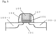
- FIG. 5 is a partial longitudinal sectional view showing an example of a semiconductor device to which the insulating film structure is applied according to the present invention shown in FIG. 2 .
- FIG. 6A to FIG. 6D are partial longitudinal sectional views in the manufacturing process of the insulating film structure comprising the silicate high dielectric constant thin film included in a semiconductor device in another embodiment according to the present invention.
- FIG. 7 is a diagram showing the metal element concentration distribution in the film thickness direction of the silicate high dielectric constant thin film included in the insulating film structure shown in FIG. 6D .
- FIG. 8A to FIG. 8D are longitudinal sectional views showing the manufacturing process of a lanthanum silicate high dielectric constant thin film included in a semiconductor device in a first example according to the present invention.
- FIG. 9 is a diagram showing an overview of constitution of vacuum evaporation apparatus used for manufacturing the lanthanum silicate high dielectric constant thin film shown in FIG. 8A to FIG. 8D .
- FIG. 10 is a diagram showing the relationship between Equivalent Oxide Thickness and leakage current found from capacity-voltage characteristics and current-voltage characteristics of the lanthanum silicate high dielectric constant thin film shown in FIG. 8D .
- FIG. 11A to FIG. 11D are longitudinal sectional views showing the manufacturing process of a hafnium silicate high dielectric constant thin film included in a semiconductor device of a second example according to the present invention.
- FIG. 12 is a diagram showing an overview of the constitution of sputter-deposition apparatus used for the manufacturing process of the hafnium silicate high dielectric constant thin film shown in FIG. 11A to FIG. 11D .
- FIG. 1A to FIG. 1D are partial longitudinal sectional views in a manufacturing process of an insulating film structure comprising a silicate high dielectric constant thin film included in a semiconductor device in one embodiment according to the present invention.
- FIG. 2 is a diagram showing concentration distribution of metal elements in a film thickness direction of the silicate high dielectric constant thin film included in a gate insulating film structure in one embodiment according to the present invention.
- a base silicon oxide film 103 comprising an oxynitride film is formed, as shown in FIG. 1B .
- metal elements are supplied to the surface of the base silicon oxide film to form a metal layer 104 .
- an insulating film structure 105 including a silicate region is formed on the silicon substrate 101 by heat treatment.
- a high dielectric constant film layer comprising silicate is not directly deposited on the silicon substrate 101 , but the insulating film structure 105 including the silicate region is formed on the silicon substrate 101 as a high dielectric constant thin film by causing an interface reaction between the base silicon oxide film 103 and the metal layer 104 by heat treatment.
- a high quality base silicon oxide film 103 is formed on the surface of the silicon substrate 101 , as shown in FIG. 1B .
- the silicon substrate 101 is being given the hydrogen termination treatment which eliminates unstable dangling bonds by binding a surface termination hydrogen 102 with remaining valence arms of silicon atoms.
- a film thickness of the base silicon oxide film 103 is preferably set thickly as compared with normally 0.6 nm or less which is a film thickness of a conventional surface insertion layer, and an electrical film thickness of the insulating film structure 105 which is finally required, namely, the base silicon oxide film 103 as thick as Equivalent Oxide Thickness is formed.
- the insulating film structure 105 includes a silicate region 105 - 2 which acts as the high dielectric constant film into which metal elements are introduced by the interface reaction, and a silicon oxide region 105 - 1 into which no metal elements are introduced.
- a formation method of the base silicon oxide film 103 shown in FIG. 1B needs no particular limits, but may adopt a known thermal oxide film formation process as one typical example.
- the base silicon oxide film 103 is required to be ultrathin as thin as the Equivalent Oxide Thickness of a high dielectric constant gate insulating film structure 105 which is finally formed, so that RTO (Rapid Thermal Oxidation) is useful.
- RTO Rapid Thermal Oxidation
- chemical oxide formed by wet processing is capable of easily forming an ultrathin base silicon oxide film 103 , but has the possibility to exert little effect in the present invention due to inferiority in interface electrical characteristics.
- the film thickness of the base silicon oxide film 103 which is formed on the surface of the silicon substrate 101 that is, the film thickness of the base silicon oxide film 103 before the interface reaction is caused be reduced, as a process shown in FIG. 1B .
- the film thickness of the base silicon oxide film 103 be normally not less than 1 nm.
- the film thickness of the base silicon oxide film may be reduced to the extent of approximately 0.6 nm at minimum.
- an oxynitride film in which trace nitrogen, for example, as much as a few percent is introduced into the base silicon oxide film 103 is used as a base layer.
- useful is a structure in which the surface of the base silicon oxide film 103 is selectively nitrided by a radical nitriding process such that nitrogen is not segregated into the interface.
- metal elements constituting silicate are supplied onto the surface of the base silicon oxide film 103 , and then the metal elements are diffused into the base silicon oxide film 103 by the heat treatment process carried out either during or after supplying the metal elements to form a silicate layer 105 - 2 in which silicon oxidation is converted into silicate, in a region except for the vicinity region of the interface with the silicon substrate 101 which is part of the base silicon oxide film 103 , in particular, on an upper layer portion of the base silicon oxide film 103 .
- a physical evaporation method such as a CVD chemical method and sputter deposition is conceivable as a means for supplying the metal elements to the surface of the base silicon oxide film 103 .
- oxidation rate of the metal elements constituting the high dielectric constant film is very fast, it is preferable to adopt an ultrahigh vacuum sputtering method which is capable of reducing residual oxygen partial pressure in treatment atmosphere during a formation process of the metal layer 104 shown in FIG. 1B to 1 ⁇ 10 ⁇ 6 Torr or less.
- metal deposition by a sputtering method requires to reduce damage to the base silicon oxide film 103 during the deposition, and outweighs spacing a distance between a sputter evaporation source and the silicon substrate 101 and supplying metal on condition that fast ions or a large amount of photons do not enter the silicon substrate 101 .
- a distance between an evaporation source and a substrate wafer needs to be not less than 100 mm, and a remote type of deposition apparatus having secured a distance of not less than 200 mm is preferable.
- an ideal method of supplying metal includes a vacuum evaporation method by electron beam heating of metallic materials, and the like.
- Atomospheric gas and a degree of vacuum are important, as described above. More specifically, it is difficult to maintain an ideal interface with the silicon substrate 101 because in conventional deposition methods by metal evaporation in oxygen atmosphere, such as reactive sputtering and reactive evaporation, an oxidation reaction progresses along with supply of the metal elements to form a stoichiometric metal oxide, leading to a progress of the interface reaction from an early stage of the deposition.
- the metal elements are supplied onto the base silicon oxide film 103 of not less than 1 nm which is ever-thicker, on condition that the residual oxygen partial pressure is 1 ⁇ 10 ⁇ 6 Torr or less during supplying the metal elements as with the present invention, part of the metal elements might come into an oxidized state by an effect of trace residual oxygen, but an interface structure between the base silicon oxide film 103 and the silicon substrate 101 is well preserved.
- the interface reaction is accelerated in an oxidation process of a metal reaction region containing a large amount of oxygen deficiencies.
- Zr elements are supplied to the base silicon oxide film 103 by use of the vacuum evaporation method on condition that the residual oxygen partial pressure is 1 ⁇ 10 ⁇ 6 Torr or less, no changes will occur in a state of Si—O bonding in a film of the base silicon oxide film 103 , and most of the Zr elements will be oxidized even under the aforementioned residual oxygen partial pressure due to very fast oxidation rate of the Zr elements.
- the interface between the high dielectric constant thin film such as HfO 2 and ZrO 2 and the silicon substrate 101 is thermally stable.
- metal elements constituting the silicate layer 105 - 2 which is a high dielectric constant film is supplied onto the surface of the base silicon oxide film 103 .
- Metal-O bonding which is a bonding of a metal atom with an oxygen atom, is stronger than Si—O bonding, so that silicate bonding (Metal-O—Si) will be formed, and an interface silicate formation reaction may be driven by temperature rise of the substrate during supplying the metal elements or the heat treatment process after supplying the metal elements. Consequently, the interface reaction will be accelerated faster than interface oxidation rate through the metallic oxide having stoichiometric film composition.
- the temperature rise of the silicon substrate 101 is also effective. Oxidation of the metal layer 104 is likely to progress even in reduced residual oxygen partial pressure apparatus because of very fast oxidation rate of the metal elements. Accordingly, it is useful to cause the temperature rise of the silicon substrate 101 during supplying the metal elements to accelerate a reaction with the base silicon oxide film 103 , namely, metal element diffusion at the same time as supplying the metal elements.
- a temperature of the silicon substrate 101 is made room temperature, a large amount of the oxygen deficiencies are present in the metal reaction region as described above. Therefore, even if the heat treatment is carried out after supplying the metal elements, the interface reaction, namely, the metal element diffusion is accelerated.
- conditions for the heat treatment process include a condition under which oxygen partial pressure is reduced with the primary object of the metal element diffusion, and a condition under which atmosphere contains oxygen with the primary object of oxygen deficiency reduction.
- the oxygen deficiency reduction in the silicate layer 105 - 2 progresses even under trace oxygen partial pressure, so that the oxygen partial pressure during the heat treatment may be reduced to achieve a condition under which oxidation of the interface between the base silicon oxide film 103 and the silicon substrate 101 is arrested.
- This provides a structure in which optimizing process conditions for the metal element diffusion into the base silicon oxide film 103 prevents the metal elements from reaching the interface between the base silicon oxide film 103 and the silicon substrate 101 , as well as provides the insulating film structure 105 composed of a silicon oxide region 105 - 1 , a silicate region 105 - 2 , and a metal rich region 105 - 3 , as shown in FIG. 1D .
- metal element concentration is highest on the surface of the insulating film structure 105 , and decreases with increasing the depth of the insulating film structure 105 , resulting in approximately zero of the metal element concentration at a certain depth from the surface of the insulating film structure 105 . More specifically, no metal elements are diffused in a region near the interface with the silicon substrate 101 , so that the metal element concentration is substantially zero. In other words, in the insulating film structure 105 , a region near the interface with the silicon substrate 101 gets into the silicon oxide region 105 - 1 not containing metal elements.
- the interface structure as good quality as that provided immediately after the base silicon oxide film 103 is formed on the surface of the silicon substrate 101 in a process shown in FIG. 1B can be maintained.
- the metallic composition is high in an upper portion of the insulating film structure 105 , whereas on the surface of the insulating film structure 105 , a metal oxide not containing silicon, or metal rich silicate is determined, depending upon a metal diffusion process or a heat treatment condition.
- the upper region comprising this metal oxide or metal rich silicate is called the metal rich region 105 - 3 .
- a region between the silicon oxide region 105 - 1 and the metal rich region 105 - 3 is called the silicate region 105 - 2 .
- the silicate region 105 - 2 has composition modulation, and the metal element concentration, namely, metallic composition increases and silicon composition decreases as closer to the metal rich region 105 - 3 , whereas the metal element concentration, namely, the metallic composition decreases and the silicon composition increases as closer to the silicon oxide region 105 - 1 .
- the insulating film structure 105 abuts on the silicon substrate 101 , and comprises the following regions: one being the silicon oxide region 105 - 1 into which no metal elements are introduced by the aforementioned interface reaction, one being a composition-modulated silicate region 105 - 2 extending on the silicon oxide region 105 - 1 and having the composition modulation by introduction of the metal elements associated with the aforementioned interface reaction, and one being the metal rich silicate region 105 - 3 extending on the silicate region 105 - 2 and having high metal element concentration, namely, metallic composition.
- a gate electrode 106 formed on the insulating film structure 105 containing the silicate region is shown in FIG. 2 .
- the metal elements supplied onto the surface of the base silicon oxide film 103 to form silicate include Zr, Hf, Ta, Al, Ti and Nb, or Sc and Y which are rare-earth elements, or La, Ce, Pr, Nd, Sm, Eu, Gd, Tb, Dy, Ho, Er, Tm, Yb, and Lu which are lanthanoid series.
- a fabrication method of the high dielectric constant film proposed by the present invention may be applied to all of these metal elements, but metal diffusion rate into the base silicon oxide film 103 varies depending upon the difference in material properties. For example, a lanthanoid oxide represented by La has properties of being likely to mix with a silicon oxide, and the metal diffusion into the base silicon oxide film 103 relatively easily progresses.
- the film thickness of a metal deposition layer dependent on metal supply is an important process parameter which determines the properties of a semiconductor device due to the following reasons.
- the film thickness of the metal deposition is thicker than necessary, despite a progress of silicate formation in the interface with the base silicon oxide film, the metallic composition is high in the upper portion of the metal layer, and in some cases, a thick metal oxide layer not containing silicon is formed.
- This metal oxide layer not containing silicon has a high relative dielectric constant, and is effective in reducing leakage current which passes through a gate insulating film, but the thermal stability deteriorates.
- a problem involved in the reliability such that device operating voltage shifts occurs. Therefore, in formation of a silicate high dielectric gate insulating film excellent in electrical characteristics, it is important to optimize the film thickness of the metal deposition layer in addition to optimization of the aforementioned base oxide film thickness.
- the unreacted regions in the metal layer 104 may be removed or separated to utilize only regions formed by the interface reaction with the base silicon oxide film as the gate insulating film.
- FIG. 3A is a longitudinal sectional view showing the insulating film structure 105 in which an unreacted region 105 - 5 is left on the upper portion of the metal layer 104 by the interface reaction between the metal layer 104 and the base silicon oxide film 103 in FIG. 1C .
- the insulating film structure 105 shown in FIG. 3A is a longitudinal sectional view showing the insulating film structure 105 in which an unreacted region 105 - 5 is left on the upper portion of the metal layer 104 by the interface reaction between the metal layer 104 and the base silicon oxide film 103 in FIG. 1C .
- 3A includes the following regions: one being the silicon oxide region 105 - 1 which abuts on the silicon substrate 101 , and into which no metal elements are introduced by the aforementioned interface reaction, one being the composition-modulated silicate region 105 - 2 which extends on the silicon oxide region 105 - 1 , and has the composition modulation by introduction of the metal elements associated with the aforementioned interface reaction, one being the metal rich silicate region 105 - 3 which extends on the silicate region 105 - 2 , and has high metal element concentration, namely, metallic composition, and one being an upper unreacted metal region 105 - 5 which extends on the metal rich silicate region 105 - 3 .
- FIG. 3B is a longitudinal sectional view showing the insulating film structure 105 after the upper unreacted region 105 - 5 shown in FIG. 3A has been removed, followed by further carrying out the reforming heat treatment.
- the unreacted metal region 105 - 5 is capable of being removed, for example, by etching.
- a wet etching solution a solution based on a diluted hydrofluoric solution or an ammonia peroxide solution may be used.
- the characteristics of the gate insulating film may be improved by giving additional heat treatment subsequent to a process of removing the unreacted metal region 105 - 5 .
- the heat treatment process for implementing the metal diffusion into the base silicon oxide film 103 from the metal layer 104 shown in FIG. 1C is carried out in reducing atmosphere, thereby making it possible to more effectively implement the diffusion reaction of the metal into the base silicon oxide film 103 .
- This is intended to cause oxygen deficiencies in the aforementioned upper reacted region to accelerate the metal diffusion into the base silicon oxide film 103 by carrying out the heat treatment on condition that oxygen atoms are taken from the metal diffusion.
- Hydrogen atmosphere and ammonia atmosphere are effective as the aforementioned reducing atmosphere.
- nitrogen introduction into the films is effective in improving thermal resistance of the high dielectric constant film.
- the aforementioned nitride process includes the heat treatment in ammonia, or nitrogen plasma treatment.
- a cap layer comprising a silicon nitride film with a film thickness of 1.0 nm or less, and preferably 0.5 nm or less, or a cap layer comprising a silicon oxynitride film, with the aim to suppress the interface reaction between a high dielectric constant insulating film 105 and the gate electrode 106 after forming the aforementioned various high dielectric constant gate insulating films 105 and before forming the gate electrode 106 .
- Effective is the gate insulating film structure characterized in that a high quality high dielectric constant gate insulating film structure 105 has the gate insulating layer 105 with a physical film thickness of 3.5 nm or less, which is provided between the silicon substrate 101 and the gate electrode 106 , and the physical film thickness of a metal-containing silicate layer present on its upper layer portion is thinner than the film thickness of the base silicon oxide film initially formed, and shown in FIG. 1C .
- FIG. 4 is a diagram for illustrative of a relationship of thicknesses A and B, the thickness A of the metal silicate region containing metal elements, and the thickness B of the silicon oxide region not containing metal elements in the gate insulating film 105 .
- the metal silicate region containing metal elements is equivalent to the composition modulated silicate region 105 - 2 and the metal rich silicate region 105 - 3 in FIG. 3B
- the silicon oxide region not containing metal elements is equivalent to the silicon oxide region 105 - 1 in FIG. 3B .
- the thickness A of the metal silicate region is preferably 1.5 nm or less.
- FIG. 5 is a partial longitudinal sectional view showing one example of a semiconductor device to which the insulating film structure according to the present invention shown in FIG. 2 is applied.
- a Field Effect Transistor comprises the silicon substrate 101 , a source region 109 - 1 and a drain region 109 - 2 selectively formed in the silicon substrate 101 , the gate insulating film 105 having the aforementioned insulating film structure formed on the surface of the silicon substrate 101 , the gate electrode 106 formed on the gate insulating film 105 , nitride film side walls 107 formed on side walls of the gate electrode 106 , and oxide film side walls 108 formed on the nitride film side walls 107 .
- the silicon nitride film side walls 108 are preferably provided with the aim to protect a gate side wall portion exposed after gate etching.
- the aforementioned high dielectric constant gate film is characterized in that hysteresis of a gate capacity-gate voltage curve by an applied bias within the device operating voltage is 5 mV or less.
- the aforementioned description has indicated a process of forming the metal layer which is to be a metal diffusion source, on the base silicon oxide film to heat-treat this laminated structure as silicate formation using the interface reaction between the silicon oxide film and the metal layer.
- an upper cap layer is further formed on the metal layer, and then the heat treatment is given to cause the metal diffusion from the metal layer into the upper cap layer and the base silicon oxide film, both of which are above and under the metal layer, to form the metal silicate gate insulating film having the component modulation.
- FIG. 6A to 6D are partial longitudinal sectional views in the manufacturing process of the insulating film structure comprising the silicate high dielectric constant thin film included in a semiconductor device in another embodiment according to the present invention.
- the base silicon oxide film 103 is formed on the silicon substrate 101 .
- the metal elements are supplied onto the surface of the base silicon oxide film 103 to form the metal layer 104 .
- a cap layer 110 is formed on the metal layer 104 .
- the insulating film structure 105 including the silicate region is formed on the silicon substrate 101 by the heat treatment.
- a high dielectric constant film layer comprising silicate is not directly deposited on the silicon substrate 101 , but the metal is thermally diffused from the metal layer 104 into the base silicon oxide film 103 and the cap layer 110 to form the insulating film structure 105 including the silicate region shown in FIG.
- An insulating film structure 105 ′ may be selected from the following regions: one being the silicon oxide region 105 - 1 which extends on the silicon substrate 101 , and into which no metal elements are introduced, one being a first silicate region 105 - 2 which extends on the silicon oxide region 105 - 1 and into which the metal elements are thermally diffused by the aforementioned silicate reaction, one being the metal rich region 105 - 3 which extends on the first silicate region 105 - 2 , and one being a second silicate region 105 - 4 which extends on the metal rich region 105 - 3 , and into which the metal elements are thermally diffused by the aforementioned silicate reaction.
- the aforementioned base silicon oxide film 103 may be selected from a combination of a silicon oxide film and a silicon oxynitride film.
- the cap layer 110 may be selected from the combinations of a silicon layer, a silicon oxide film layer, a silicon nitride layer, and a silicon oxynitride film layer. Furthermore, it is effective to use ultra-thin films of 1 nm or less, preferably 0.5 nm or less as the film thickness of the cap layer 110 . Note that the description overlapped with the aforementioned manufacturing process referring to FIG. 1A to FIG. 1D will be omitted to avoid redundancy.
- FIG. 7 is a diagram showing the metal element concentration distribution in the film thickness direction of the silicate high dielectric constant thin film included in the insulating film structure 105 ′ shown in FIG. 6D .
- the metal element concentration is highest in the metal rich region 105 - 3 , and decreases with increasing the distance from the metal rich region 105 - 3 in the first and second silicate regions 105 - 2 and 105 - 4 .
- the metal element concentration decreases with increasing the depth
- the metal element concentration increases with increasing the depth. That is, in a region close to the interface with the silicon substrate 101 , no metal elements are diffused, so that the metal element concentration is substantially zero. Namely, in the insulating film structure 105 ′, the region close to the interface with the silicon substrate 101 is the silicon oxide region 105 - 1 not containing metal elements.
- FIG. 8A to FIG. 8D are longitudinal sectional views showing a manufacturing process of a lanthanum silicate high dielectric constant thin film included in a semiconductor device in a first example according to the present invention.
- FIG. 9 is a diagram showing an overview of constitution of vacuum evaporation apparatus used for manufacturing the lanthanum silicate high dielectric constant thin film shown in FIG. 8A to FIG. 8D .
- FIG. 10 is a diagram showing a relationship between Equivalent Oxide Thickness and leakage current which are found from capacity-voltage characteristics and current-voltage characteristics of the lanthanum silicate high dielectric constant thin film shown in FIG. 8D .
- a base silicon oxide film 103 was formed as a base layer
- a lanthanum silicate high dielectric constant thin film 205 was formed using La as a metal element
- characteristics of the semiconductor device were verified using the lanthanum silicate high dielectric constant thin film 205 .
- a surface oxide film was removed with hydrofluoric acid treatment, and the silicon substrate 101 was surface-oxidized by RTO to form the base silicon oxide film 103 with a film thickness of 1.1 nm.
- the RTO was carried out by making a substrate temperature 700° C. under reduced pressure oxygen conditions (500 Pa).
- the silicon substrate 101 in which the base silicon oxide film 103 was formed was mounted on a wafer transportation system 403 , and was introduced into a deposition chamber 401 through a wafer introduction chamber 402 to deposit a metal lanthanum layer 204 on the base silicon oxide film 103 by electron beam heating (electron-beam evaporation) of an LA evaporation source using an electron beam evaporation mechanism 406 .
- a degree of vacuum of the deposition chamber 401 was set to a condition of 2 ⁇ 10 ⁇ 9 Torr or less by vacuuming with a roughing vacuum pump 408 and a main air pump 407 , and a substrate temperature of the silicon substrate 101 was set to 500° C. by room temperature and heating of a substrate heating mechanism 405 .
- the silicon substrate 101 on which the metal lanthanum layer 204 was deposited was taken out of the deposition chamber 401 , and the heat treatment was carried out in nitrogen atmosphere at 500° C. for 10 minutes for the sake of compensation for oxygen deficiencies in the film to form the lanthanum silicate high dielectric constant thin film 205 composed of a silicon oxide film region 205 - 1 , an La silicate region 205 - 2 , and an La rich region 205 - 3 .
- a heat treatment process may be carried out using a horizontal quartz reactor to cause oxygen introduction into a film and metal diffusion into the base silicon oxide film 103 by means of residual oxygen in treatment atmosphere or adsorption oxygen in wafer transportation.
- FIG. 10 shows respective characteristic results of samples subjected to comparison under different conditions that a temperature of the silicon substrate 101 during lanthanum deposition was room temperature and 500° C., which reveals that the leakage current is reduced in all the samples, as compared with the base silicon oxide film 103 .
- the samples subjected to the comparison carried out by making the temperature of the silicon substrate 101 a temperature of 500° C. during the lanthanum deposition showed that the Equivalent Oxide Thickness was thinner than the film thickness of the base silicon oxide film 103 , from which it was confirmed that lanthanum was diffused into the base silicon oxide film 103 , and high dielectricity advanced by the aforementioned manufacturing method of the present invention.
- the thinnest sample of the Equivalent Oxide Thickness among the samples subjected to the comparison carried out by making the temperature of the silicon substrate 101 room temperature during the lanthanum deposition showed that the Equivalent Oxide Thickness was thinner than the film thickness of the base silicon oxide film 103 , from which it was confirmed that the high dielectricity by metal diffusion advanced even on condition that the temperature of the silicon substrate 101 was room temperature.
- the Equivalent Oxide Thickness had a tendency to be thin in the samples whose substrate temperatures are high during the lanthanum deposition, whereby effects in providing temperature rise to the silicon substrate 101 during the lanthanum deposition were confirmed.
- defect density was reduced to 1 ⁇ 5 to 1/10 by applying the manufacturing method of the present invention, as compared with the case where the lanthanum silicate was directly deposited on the silicon substrate 101 .
- the lanthanum silicate high dielectric constant thin film 205 a gate insulating film to prototype the MOSFET using a polysilicon gate electrode, the mobility increased by not less than 50%, as compared with the case where the lanthanum silicate was directly deposited on the silicon substrate 101 .
- FIG. 11A to FIG. 11D are longitudinal sectional views showing a manufacturing process of a hafnium silicate high dielectric constant thin film included in a semiconductor device of a second example according to the present invention.
- FIG. 12 is a diagram showing an overview of constitution of sputter deposition apparatus used for the manufacturing process of the hafnium silicate high dielectric constant thin film shown in FIG. 11A to FIG. 11D .
- a silicon oxynitride film 203 was formed as a base layer, and a hafnium silicate high dielectric constant thin film 305 was formed using Hf as a metal element, the hafnium silicate high dielectric constant thin film 305 being used to verify characteristics of a semiconductor device.
- the reason for which the silicon oxynitride film 203 was used as a base oxide film in the second example was for the sake of improvement in thermal resistance by addition of nitrogen to high dielectric constant materials.
- a surface oxide film was removed with hydrofluoric acid treatment to surface-oxidize the silicon substrate 101 by RTO, forming a base silicon oxide film 103 with a film thickness of 1.5 nm.
- the RTO was carried out by making a substrate temperature 700° C. under reduced pressure oxygen conditions (500 Pa).
- nitride treatment for a surface of the base silicon oxide film 103 was carried out by means of vacuum apparatus on which an ECR (Electron Cyclotron Resonance) radical source was mounted as a plasma source to form the silicon oxynitride film 203 .
- the nitride treatment was carried out under irradiation conditions of nitrogen radical at a substrate temperature of 500° C., nitrogen pressure of 0.3 Pa, and input power of 100 W.
- the silicon substrate 101 in which the silicon oxynitride film 203 was formed was mounted on a wafer transportation system 703 , and introduced into a deposition chamber 701 , which was ultrahigh vacuum-enabled remote type of sputter apparatus, through a wafer introduction chamber 702 .
- a sputter evaporation mechanism 706 was then used to carry out metal layer deposition making an Hf target evaporation source and argon sputter gas to deposit an hafnium deposition layer 304 on the silicon oxynitride film 203 .
- a degree of vacuum of the deposition chamber 701 was set to a condition of 5 ⁇ 10 ⁇ 9 Torr or less by vacuuming with a roughing vacuum pump 708 and a main air pump 707 , the substrate temperature of the silicon substrate 101 was set to room temperature, distance between a sputter source and a wafer was set to 300 mm for reducing damage, argon gas partial pressure was set to 0.05 Pa, and input power was set to 500 W.
- Effective Oxide Thickness was 1.45 nm, and that leakage current was capable of being reduced by three to four digits more than that of a silicon oxide film.
- the manufacturing method of the present invention was applied to thereby reduce interface defect density by approximately 1 ⁇ 5, as compared with the case where HfO 2 was directly deposited on the base silicon oxide film 103 having a thickness of 0.5 nm by a reactive sputtering method in accordance with the prior art. Furthermore, as a result of having evaluated heat treatment-crystallization temperature by the heat treatment, thermal resistance was improved by 50° C. to 100° C. with respect to the hafnium silicate high dielectric constant thin film 305 into which nitrogen was not introduced.
- the mobility increased by not less than 40%, as compared with the case where the hafnium silicate was directly deposited on the silicon substrate.
- the life of a device estimated from electrical defects (interface defect density: Dit) present in an interface between an insulating film and a silicon substrate, and a threshold voltage shift associated with device operation was evaluated for these devices with different film thicknesses of metallic hafnium.
- interface defect density could be reduced to less than 1 ⁇ 2, as compared with the one fabricated by making the film thickness of deposition 1.0 nm, and that the life of a device (reliability) could be improved ten times or more.
- the film thickness of the metal layer was preferably 1 nm or less, and more preferably 0.6 nm or less.
- the lower limit of the film thickness is not particularly limited as far as a silicate layer having a significant thickness is formed, but the effect is noticeable when the film thickness is, for example, not less than 0.4 nm. In making device design, any film thickness may be selected from such a film thickness range.
- silicate deposition making the thickness of a metal deposition layer a value close to 1 nm is effective.
- the silicate deposition making the thickness of the metal deposition layer 0.4 to 0.6 nm is effective.
- a typical structure of a gate insulating film achieving an effect of reducing the leakage current of the gate insulating film and improvement in transistor mobility, as well as ensuring of the reliability had a gross physical film thickness of 3.5 nm or less, and that if a physical film thickness of a base silicon oxide film region (B) not containing metal elements was thicker than the physical film thickness of a silicate region containing metal elements, namely, if a relationship of A ⁇ B was satisfied, excellent characteristics could be obtained.
- the typical example included the physical film thickness of an unreacted base silicon oxide film of 1.4 nm, the physical film thickness of a metal-containing upper silicate layer of 1.2 nm, and an electrical film thickness of 1.75 nm.
- a small transistor with a short gate length provided favorable transistor characteristics, when a side wall comprising a silicon nitride film was formed on a gate side wall.
- Hf metal was used as a metal diffusion source in the aforementioned examples, but it is useful to introduce nitrogen as sputtering gas during metal Hf deposition to deposit HfN (hafnium nitride).
- An Hf silicate film (HfSiON) was able to be fabricated by giving the heat treatment onto the base silicon oxide film with a thickness of 1.5 nm after deposition of HfN in a manner similar to the foregoing. Nitrogen remains as little as approximately 4% in the Hf silicate film because part of nitrogen in a film was thermally desorbed during the heat treatment.
- a metal layer deposition process and the heat treatment process of supplying metal elements which constitute a high dielectric constant film on a surface of the base silicon oxide film 103 allow the metal elements to be diffused into the base silicon oxide film 103 to thereby form an insulating film structure 105 including the silicate region as the gate insulating film, thereby enabling formation of a gate insulating film structure having a good quality interface between the base silicon oxide film and the silicon substrate in the interface between the high dielectric constant thin film and the silicon substrate, with an effect that improvement in interface electrical characteristics, which has been a longstanding task in practical use of the high dielectric constant thin film may be achieved.
- independent control of the metal diffusion into the base silicon oxide film 103 allows the metal elements to be diffused only onto the surface side of the base silicon oxide film 103 , making it easier to optimize conditions that no metal elements reach the interface between a silicon oxide film and the silicon substrate, with an effect that fabrication of the high dielectric gate insulating film having excellent interface electrical characteristics is enabled.
- the film thickness of metal is thinned, and the metal film is completely diffused and made into silicate to achieve silicate deposition.
- the metal film having a relatively thick film thickness is used, there is a possibility that an unreacted metal region with the base silicon oxide film could remain after the heat treatment. In this case, the unreacted metal region may be removed to use only a region made into silicate as the gate insulating film.
- first and second examples show the case where a bilayer structure of the base oxide film and the upper metal-containing layer has been used, a silicon or silicon oxide film based cap layer is further formed above the aforementioned bilayer structure before giving the heat treatment, thereby making it possible to form a structure having a silicon rich region on the uppermost layer.
- a silicon cap layer with a film thickness of 0.5 nm was formed by the sputter deposition using an Si target, after the bilayer structure comprising the silicon oxide film and metal Hf had been formed by RTO and sputter deposition similar to those of the second example. Then, treatment was carried out in oxygen atmosphere at 500° C. for two minutes, followed by giving the heat treatment in nitrogen at 900° C. The heat treatment runs formation of a surface silicon oxide film layer by oxidation of a surface silicon cap layer in parallel with the metal diffusion from a metal Hf layer into upper and lower silicon oxide layers to form the silicate layer.
- Component distribution in a thickness direction of this silicate layer is high in the lowermost portion abutting on an upper portion of the film and the silicon substrate, and low in the central portion (a portion in which the metal layer was initially formed).
- metallic (Hf) composition indicates a maximal value in the vicinity of the central portion of the film, and the Hf composition decreases as closer to a silicon interface and the uppermost portion. Namely, a structure provided with the component distribution has been provided.
- the silicon oxide film, the silicon oxynitride film, and the silicon nitride film as a surface cap layer, and further the use of a metal silicate layer, a metal aluminate layer, a metal oxide layer, and a metal nitride layer as the metal diffusion source were found to be effective.
- the metal layer deposition process and the heat treatment process of supplying metal elements which constitute the high dielectric constant film on the surface of the silicon oxide film allow the metal elements to be diffused into the silicon oxide film to thereby form the silicate layer as the gate insulating film, thereby enabling formation of the gate insulating film structure having a good quality interface between the silicon oxide film and the silicon substrate in the interface between the high dielectric constant thin film and the silicon substrate, with an effect that improvement in interface electrical characteristics, which has been a longstanding task in practical use of the high dielectric constant insulating film may be achieved.
- independent control of the metal diffusion into the silicon oxide film allows the metal elements to be diffused only onto the surface side of the silicon oxide film, making it easier to optimize the conditions that no metal elements reach the interface between the silicon oxide film and the silicon substrate, with an effect that the fabrication of the high dielectric constant gate insulating film having excellent interface electrical characteristics is enabled.
- application of the present invention is not limited to specific devices described in the aforementioned examples, as far as a semiconductor device including an insulating film structure which electrically insulates a conductive region from a silicon region is concerned.
- the insulating film structure is not limited to a gate insulating film, and the semiconductor device includes one which electrically insulates the conductive region from the silicon region.
Abstract
Description
Claims (1)
Applications Claiming Priority (3)
| Application Number | Priority Date | Filing Date | Title |
|---|---|---|---|
| JP2002-206678 | 2002-07-16 | ||
| JP2002206678 | 2002-07-16 | ||
| PCT/JP2003/009052 WO2004008544A1 (en) | 2002-07-16 | 2003-07-16 | Semiconductor device, production method and production device thereof |
Publications (2)
| Publication Number | Publication Date |
|---|---|
| US20050233526A1 US20050233526A1 (en) | 2005-10-20 |
| US7679148B2 true US7679148B2 (en) | 2010-03-16 |
Family
ID=30112802
Family Applications (1)
| Application Number | Title | Priority Date | Filing Date |
|---|---|---|---|
| US10/521,311 Expired - Fee Related US7679148B2 (en) | 2002-07-16 | 2003-07-16 | Semiconductor device, production method and production device thereof |
Country Status (5)
| Country | Link |
|---|---|
| US (1) | US7679148B2 (en) |
| JP (1) | JP4239015B2 (en) |
| CN (1) | CN100565916C (en) |
| AU (1) | AU2003281112A1 (en) |
| WO (1) | WO2004008544A1 (en) |
Cited By (2)
| Publication number | Priority date | Publication date | Assignee | Title |
|---|---|---|---|---|
| US20110027979A1 (en) * | 2009-07-28 | 2011-02-03 | Canon Anelva Corporation | Dielectric film, method of manufacutring semiconductor device using dielectric film, and semiconductor manufacturing apparatus |
| US20120074533A1 (en) * | 2010-09-24 | 2012-03-29 | Tokyo Electron (TEL)Limited | Structures And Techniques For Atomic Layer Deposition |
Families Citing this family (36)
| Publication number | Priority date | Publication date | Assignee | Title |
|---|---|---|---|---|
| JP4526995B2 (en) * | 2004-04-09 | 2010-08-18 | 東京エレクトロン株式会社 | Method for forming gate insulating film, computer-readable storage medium, and computer program |
| JP2005317647A (en) * | 2004-04-27 | 2005-11-10 | Toshiba Corp | Semiconductor device and its fabrication process |
| JP2005317583A (en) * | 2004-04-27 | 2005-11-10 | Renesas Technology Corp | Semiconductor device and its manufacturing method |
| JP4792716B2 (en) * | 2004-07-06 | 2011-10-12 | 日本電気株式会社 | Semiconductor device and manufacturing method thereof |
| JP2006054382A (en) * | 2004-08-16 | 2006-02-23 | Sony Corp | Metallic silicate film, manufacturing method thereof, semiconductor device, and manufacturing method thereof |
| WO2006022175A1 (en) * | 2004-08-23 | 2006-03-02 | Nec Corporation | Semiconductor device and method for manufacturing the same |
| JP4564310B2 (en) * | 2004-09-01 | 2010-10-20 | 株式会社日立国際電気 | Manufacturing method of semiconductor device |
| JP2006135084A (en) * | 2004-11-05 | 2006-05-25 | Fujitsu Ltd | Semiconductor device and manufacturing method therefor |
| JP4914573B2 (en) | 2005-02-25 | 2012-04-11 | キヤノンアネルバ株式会社 | Method of manufacturing field effect transistor having high dielectric gate insulating film and metal gate electrode |
| JP2006253267A (en) * | 2005-03-09 | 2006-09-21 | Sony Corp | Semiconductor device and its manufacturing method |
| JP4860183B2 (en) * | 2005-05-24 | 2012-01-25 | ルネサスエレクトロニクス株式会社 | Semiconductor device and manufacturing method thereof |
| US7812412B2 (en) * | 2005-10-04 | 2010-10-12 | Nec Corporation | Semiconductor device |
| JPWO2007138693A1 (en) * | 2006-05-31 | 2009-10-01 | 富士通株式会社 | Semiconductor device and manufacturing method thereof |
| US20080237694A1 (en) * | 2007-03-27 | 2008-10-02 | Michael Specht | Integrated circuit, cell, cell arrangement, method for manufacturing an integrated circuit, method for manufacturing a cell, memory module |
| JP5037242B2 (en) * | 2007-07-06 | 2012-09-26 | キヤノンアネルバ株式会社 | Manufacturing method of semiconductor device |
| WO2008149446A1 (en) * | 2007-06-07 | 2008-12-11 | Canon Anelva Corporation | Semiconductor production apparatus and process |
| JP2009038229A (en) * | 2007-08-02 | 2009-02-19 | Nec Electronics Corp | Semiconductor device |
| US8735243B2 (en) * | 2007-08-06 | 2014-05-27 | International Business Machines Corporation | FET device with stabilized threshold modifying material |
| JP5221121B2 (en) * | 2007-12-27 | 2013-06-26 | キヤノン株式会社 | Insulating film formation method |
| JP5136110B2 (en) * | 2008-02-19 | 2013-02-06 | ソニー株式会社 | Method for manufacturing solid-state imaging device |
| JP2009260151A (en) * | 2008-04-18 | 2009-11-05 | Tokyo Electron Ltd | Method of forming metal doped layer, film forming apparatus, and storage medium |
| JP5314964B2 (en) * | 2008-08-13 | 2013-10-16 | ルネサスエレクトロニクス株式会社 | Manufacturing method of semiconductor device |
| KR20100101450A (en) * | 2009-03-09 | 2010-09-17 | 삼성전자주식회사 | Semiconductor device and associated methods of manufacture |
| US7944004B2 (en) * | 2009-03-26 | 2011-05-17 | Kabushiki Kaisha Toshiba | Multiple thickness and/or composition high-K gate dielectrics and methods of making thereof |
| JP5372617B2 (en) | 2009-06-24 | 2013-12-18 | ルネサスエレクトロニクス株式会社 | Manufacturing method of semiconductor device |
| JPWO2011042955A1 (en) * | 2009-10-06 | 2013-02-28 | ルネサスエレクトロニクス株式会社 | Semiconductor device |
| US8343865B2 (en) * | 2010-01-21 | 2013-01-01 | Renesas Electronics Corporation | Semiconductor device having dual work function metal |
| US8598000B2 (en) | 2010-03-30 | 2013-12-03 | Volterra Semiconductor Corporation | Two step poly etch LDMOS gate formation |
| CN102214609A (en) * | 2010-04-07 | 2011-10-12 | 中国科学院微电子研究所 | Semiconductor device and manufacturing method thereof |
| JP5521726B2 (en) * | 2010-04-16 | 2014-06-18 | 富士通セミコンダクター株式会社 | Semiconductor device and manufacturing method thereof |
| US8575653B2 (en) | 2010-09-24 | 2013-11-05 | Intel Corporation | Non-planar quantum well device having interfacial layer and method of forming same |
| WO2014035933A1 (en) * | 2012-08-28 | 2014-03-06 | Applied Materials, Inc. | Methods and apparatus for forming tantalum silicate layers on germanium or iii-v semiconductor devices |
| US9698235B2 (en) * | 2013-10-22 | 2017-07-04 | National Institute Of Advanced Industrial Science And Technology | Field-effect transistor |
| JP6270667B2 (en) * | 2014-08-28 | 2018-01-31 | 三菱電機株式会社 | Semiconductor device and manufacturing method thereof |
| KR102516723B1 (en) * | 2020-12-31 | 2023-03-30 | 포항공과대학교 산학협력단 | CBRAM-Based Selection Device Doped with Ionizable Metal Ions and Method of Manufacturing the Same |
| WO2023160896A1 (en) * | 2022-02-24 | 2023-08-31 | Universiteit Twente | Pellicles and membranes for use in a lithographic apparatus |
Citations (16)
| Publication number | Priority date | Publication date | Assignee | Title |
|---|---|---|---|---|
| JPS589331A (en) | 1981-07-08 | 1983-01-19 | Mitsubishi Electric Corp | Wire bonding apparatus for semiconductor device |
| JPS6211559A (en) | 1985-07-09 | 1987-01-20 | 株式会社 タクマ | Shearing crushing device for bulky material |
| US20010023120A1 (en) | 2000-03-10 | 2001-09-20 | Yoshitaka Tsunashima | Semiconductor device having a gate insulating film structure including an insulating film containing metal, silicon and oxygen and manufacturing method thereof |
| JP2001332547A (en) | 2000-03-17 | 2001-11-30 | Toshiba Corp | Semiconductor device and its manufacturing method |
| JP2002184779A (en) | 2000-12-13 | 2002-06-28 | Shin Etsu Handotai Co Ltd | Annealed wafer and method of manufacturing the same |
| JP2002184773A (en) | 2000-12-19 | 2002-06-28 | Nec Corp | Method of forming thin film having high permittivity and method of manufacturing semiconductor device using the thin film having high permittivity |
| JP2003008011A (en) | 2001-06-21 | 2003-01-10 | Matsushita Electric Ind Co Ltd | Semiconductor device and its manufacturing method |
| JP2003158262A (en) | 2001-11-22 | 2003-05-30 | Toshiba Corp | Semiconductor device and method of manufacturing the same |
| US6586349B1 (en) * | 2002-02-21 | 2003-07-01 | Advanced Micro Devices, Inc. | Integrated process for fabrication of graded composite dielectric material layers for semiconductor devices |
| US20030127640A1 (en) | 2002-01-08 | 2003-07-10 | Kabushiki Kaisha Toshiba | Semiconductor device and method for manufacturing semiconductor device |
| US20030137019A1 (en) * | 2000-01-19 | 2003-07-24 | Jon-Paul Maria | Lanthanum Oxide-Based Dielectrics for Integrated Circuit Capacitors |
| US20030219972A1 (en) * | 2002-05-22 | 2003-11-27 | Green Martin L. | Fabrication process for a semiconductor device having a metal oxide dielectric material with a high dielectric constant, annealed with a buffered anneal process |
| US6703277B1 (en) * | 2002-04-08 | 2004-03-09 | Advanced Micro Devices, Inc. | Reducing agent for high-K gate dielectric parasitic interfacial layer |
| JP2004259906A (en) | 2003-02-26 | 2004-09-16 | Toshiba Corp | Semiconductor device and method of manufacturing the same |
| US20050009371A1 (en) * | 2002-06-14 | 2005-01-13 | Metzner Craig R. | System and method for forming a gate dielectric |
| US20060054980A1 (en) * | 2001-02-02 | 2006-03-16 | Jong-Pyo Kim | Dielectric multilayer structures of microelectronic devices and methods for fabricating the same |
Family Cites Families (2)
| Publication number | Priority date | Publication date | Assignee | Title |
|---|---|---|---|---|
| JPS5893331A (en) * | 1981-11-30 | 1983-06-03 | Toshiba Corp | Forming method for insulating film in semiconductor device |
| JPS62118559A (en) * | 1985-11-18 | 1987-05-29 | Nec Corp | Semiconductor device |
-
2003
- 2003-07-16 CN CNB038170663A patent/CN100565916C/en not_active Expired - Fee Related
- 2003-07-16 US US10/521,311 patent/US7679148B2/en not_active Expired - Fee Related
- 2003-07-16 AU AU2003281112A patent/AU2003281112A1/en not_active Abandoned
- 2003-07-16 JP JP2004521225A patent/JP4239015B2/en not_active Expired - Fee Related
- 2003-07-16 WO PCT/JP2003/009052 patent/WO2004008544A1/en active Application Filing
Patent Citations (18)
| Publication number | Priority date | Publication date | Assignee | Title |
|---|---|---|---|---|
| JPS589331A (en) | 1981-07-08 | 1983-01-19 | Mitsubishi Electric Corp | Wire bonding apparatus for semiconductor device |
| JPS6211559A (en) | 1985-07-09 | 1987-01-20 | 株式会社 タクマ | Shearing crushing device for bulky material |
| US20030137019A1 (en) * | 2000-01-19 | 2003-07-24 | Jon-Paul Maria | Lanthanum Oxide-Based Dielectrics for Integrated Circuit Capacitors |
| US20010023120A1 (en) | 2000-03-10 | 2001-09-20 | Yoshitaka Tsunashima | Semiconductor device having a gate insulating film structure including an insulating film containing metal, silicon and oxygen and manufacturing method thereof |
| JP2001257344A (en) | 2000-03-10 | 2001-09-21 | Toshiba Corp | Semiconductor device and manufacturing method of semiconductor device |
| JP2001332547A (en) | 2000-03-17 | 2001-11-30 | Toshiba Corp | Semiconductor device and its manufacturing method |
| JP2002184779A (en) | 2000-12-13 | 2002-06-28 | Shin Etsu Handotai Co Ltd | Annealed wafer and method of manufacturing the same |
| JP2002184773A (en) | 2000-12-19 | 2002-06-28 | Nec Corp | Method of forming thin film having high permittivity and method of manufacturing semiconductor device using the thin film having high permittivity |
| US20060054980A1 (en) * | 2001-02-02 | 2006-03-16 | Jong-Pyo Kim | Dielectric multilayer structures of microelectronic devices and methods for fabricating the same |
| JP2003008011A (en) | 2001-06-21 | 2003-01-10 | Matsushita Electric Ind Co Ltd | Semiconductor device and its manufacturing method |
| JP2003158262A (en) | 2001-11-22 | 2003-05-30 | Toshiba Corp | Semiconductor device and method of manufacturing the same |
| US20030127640A1 (en) | 2002-01-08 | 2003-07-10 | Kabushiki Kaisha Toshiba | Semiconductor device and method for manufacturing semiconductor device |
| JP2003204061A (en) | 2002-01-08 | 2003-07-18 | Toshiba Corp | Semiconductor device and method of manufacturing semiconductor device |
| US6586349B1 (en) * | 2002-02-21 | 2003-07-01 | Advanced Micro Devices, Inc. | Integrated process for fabrication of graded composite dielectric material layers for semiconductor devices |
| US6703277B1 (en) * | 2002-04-08 | 2004-03-09 | Advanced Micro Devices, Inc. | Reducing agent for high-K gate dielectric parasitic interfacial layer |
| US20030219972A1 (en) * | 2002-05-22 | 2003-11-27 | Green Martin L. | Fabrication process for a semiconductor device having a metal oxide dielectric material with a high dielectric constant, annealed with a buffered anneal process |
| US20050009371A1 (en) * | 2002-06-14 | 2005-01-13 | Metzner Craig R. | System and method for forming a gate dielectric |
| JP2004259906A (en) | 2003-02-26 | 2004-09-16 | Toshiba Corp | Semiconductor device and method of manufacturing the same |
Cited By (4)
| Publication number | Priority date | Publication date | Assignee | Title |
|---|---|---|---|---|
| US20110027979A1 (en) * | 2009-07-28 | 2011-02-03 | Canon Anelva Corporation | Dielectric film, method of manufacutring semiconductor device using dielectric film, and semiconductor manufacturing apparatus |
| US8288234B2 (en) | 2009-07-28 | 2012-10-16 | Canon Anelva Corporation | Method of manufacturing hafnium-containing and silicon-containing metal oxynitride dielectric film |
| US20120074533A1 (en) * | 2010-09-24 | 2012-03-29 | Tokyo Electron (TEL)Limited | Structures And Techniques For Atomic Layer Deposition |
| US8722548B2 (en) * | 2010-09-24 | 2014-05-13 | International Business Machines Corporation | Structures and techniques for atomic layer deposition |
Also Published As
| Publication number | Publication date |
|---|---|
| US20050233526A1 (en) | 2005-10-20 |
| CN100565916C (en) | 2009-12-02 |
| JP4239015B2 (en) | 2009-03-18 |
| AU2003281112A1 (en) | 2004-02-02 |
| CN1669153A (en) | 2005-09-14 |
| WO2004008544A1 (en) | 2004-01-22 |
| JPWO2004008544A1 (en) | 2005-11-17 |
Similar Documents
| Publication | Publication Date | Title |
|---|---|---|
| US7679148B2 (en) | Semiconductor device, production method and production device thereof | |
| JP4643884B2 (en) | Semiconductor device and manufacturing method thereof | |
| US10068771B2 (en) | System and method for mitigating oxide growth in a gate dielectric | |
| US6884685B2 (en) | Radical oxidation and/or nitridation during metal oxide layer deposition process | |
| JP4104834B2 (en) | Manufacturing method of MIS field effect transistor | |
| JP2003069011A (en) | Semiconductor device and method of manufacturing the same | |
| US7601578B2 (en) | Defect control in gate dielectrics | |
| JP2009177161A (en) | Method for forming insulation film | |
| US7141466B2 (en) | Method of fabricating semiconductor device having gate insulating film comprising a silicate nitride film with interface insulating film | |
| JP2001332547A (en) | Semiconductor device and its manufacturing method | |
| WO2005038929A1 (en) | Method for manufacturing semiconductor device | |
| JP2000049349A (en) | Manufacture for field-effect device in integrated circuit | |
| JP4358504B2 (en) | Method for manufacturing nonvolatile semiconductor memory device | |
| JP2001085427A (en) | Oxynitride film and forming method therefor | |
| JPWO2006009025A1 (en) | Semiconductor device and manufacturing method of semiconductor device | |
| US20080128833A1 (en) | High-Dielectric-Constant Film, Field-Effect Transistor and Semiconductor Integrated Circuit Device Using the Same, and Method for Producing High-Dielectric-Constant Film | |
| JPWO2004073072A1 (en) | MIS type semiconductor device and method for manufacturing MIS type semiconductor device | |
| US20050189598A1 (en) | Logic embedded-memory integrated circuits |
Legal Events
| Date | Code | Title | Description |
|---|---|---|---|
| AS | Assignment |
Owner name: NEC CORPORATION, JAPAN Free format text: ASSIGNMENT OF ASSIGNORS INTEREST;ASSIGNORS:WATANABE, HEIJI;WATANABE, HIROHITO;TATSUMI, TORU;AND OTHERS;REEL/FRAME:016726/0750 Effective date: 20040830 Owner name: NEC CORPORATION,JAPAN Free format text: ASSIGNMENT OF ASSIGNORS INTEREST;ASSIGNORS:WATANABE, HEIJI;WATANABE, HIROHITO;TATSUMI, TORU;AND OTHERS;REEL/FRAME:016726/0750 Effective date: 20040830 |
|
| STCF | Information on status: patent grant |
Free format text: PATENTED CASE |
|
| AS | Assignment |
Owner name: NEC ELECTRONICS CORPORATION,JAPAN Free format text: ASSIGNMENT OF ASSIGNORS INTEREST;ASSIGNOR:NEC CORPORATION;REEL/FRAME:024524/0463 Effective date: 20100331 Owner name: NEC ELECTRONICS CORPORATION, JAPAN Free format text: ASSIGNMENT OF ASSIGNORS INTEREST;ASSIGNOR:NEC CORPORATION;REEL/FRAME:024524/0463 Effective date: 20100331 |
|
| AS | Assignment |
Owner name: RENESAS ELECTRONICS CORPORATION, JAPAN Free format text: CHANGE OF NAME;ASSIGNOR:NEC ELECTRONICS CORPORATION;REEL/FRAME:025525/0145 Effective date: 20100401 |
|
| FPAY | Fee payment |
Year of fee payment: 4 |
|
| MAFP | Maintenance fee payment |
Free format text: PAYMENT OF MAINTENANCE FEE, 8TH YEAR, LARGE ENTITY (ORIGINAL EVENT CODE: M1552) Year of fee payment: 8 |
|
| AS | Assignment |
Owner name: RENESAS ELECTRONICS CORPORATION, JAPAN Free format text: CHANGE OF ADDRESS;ASSIGNOR:RENESAS ELECTRONICS CORPORATION;REEL/FRAME:044928/0001 Effective date: 20150806 |
|
| FEPP | Fee payment procedure |
Free format text: MAINTENANCE FEE REMINDER MAILED (ORIGINAL EVENT CODE: REM.); ENTITY STATUS OF PATENT OWNER: LARGE ENTITY |
|
| LAPS | Lapse for failure to pay maintenance fees |
Free format text: PATENT EXPIRED FOR FAILURE TO PAY MAINTENANCE FEES (ORIGINAL EVENT CODE: EXP.); ENTITY STATUS OF PATENT OWNER: LARGE ENTITY |
|
| STCH | Information on status: patent discontinuation |
Free format text: PATENT EXPIRED DUE TO NONPAYMENT OF MAINTENANCE FEES UNDER 37 CFR 1.362 |
|
| FP | Lapsed due to failure to pay maintenance fee |
Effective date: 20220316 |