US7656142B2 - Switching regulator with variable slope compensation - Google Patents
Switching regulator with variable slope compensation Download PDFInfo
- Publication number
- US7656142B2 US7656142B2 US11/180,556 US18055605A US7656142B2 US 7656142 B2 US7656142 B2 US 7656142B2 US 18055605 A US18055605 A US 18055605A US 7656142 B2 US7656142 B2 US 7656142B2
- Authority
- US
- United States
- Prior art keywords
- signal
- switching
- duty cycle
- regulator
- circuit
- Prior art date
- Legal status (The legal status is an assumption and is not a legal conclusion. Google has not performed a legal analysis and makes no representation as to the accuracy of the status listed.)
- Active, expires
Links
- 230000001419 dependent effect Effects 0.000 claims abstract description 5
- 238000001514 detection method Methods 0.000 claims description 11
- 230000003252 repetitive effect Effects 0.000 claims description 6
- 230000001360 synchronised effect Effects 0.000 claims description 2
- 238000000034 method Methods 0.000 claims 6
- 230000000977 initiatory effect Effects 0.000 claims 3
- 230000008878 coupling Effects 0.000 claims 2
- 238000010168 coupling process Methods 0.000 claims 2
- 238000005859 coupling reaction Methods 0.000 claims 2
- 238000010586 diagram Methods 0.000 description 13
- 239000003990 capacitor Substances 0.000 description 7
- 230000004044 response Effects 0.000 description 3
- 230000008859 change Effects 0.000 description 2
- 230000007423 decrease Effects 0.000 description 2
- 230000004048 modification Effects 0.000 description 2
- 238000012986 modification Methods 0.000 description 2
- 230000004913 activation Effects 0.000 description 1
- 230000010355 oscillation Effects 0.000 description 1
Images


Classifications
-
- H—ELECTRICITY
- H02—GENERATION; CONVERSION OR DISTRIBUTION OF ELECTRIC POWER
- H02M—APPARATUS FOR CONVERSION BETWEEN AC AND AC, BETWEEN AC AND DC, OR BETWEEN DC AND DC, AND FOR USE WITH MAINS OR SIMILAR POWER SUPPLY SYSTEMS; CONVERSION OF DC OR AC INPUT POWER INTO SURGE OUTPUT POWER; CONTROL OR REGULATION THEREOF
- H02M3/00—Conversion of dc power input into dc power output
- H02M3/02—Conversion of dc power input into dc power output without intermediate conversion into ac
- H02M3/04—Conversion of dc power input into dc power output without intermediate conversion into ac by static converters
- H02M3/10—Conversion of dc power input into dc power output without intermediate conversion into ac by static converters using discharge tubes with control electrode or semiconductor devices with control electrode
- H02M3/145—Conversion of dc power input into dc power output without intermediate conversion into ac by static converters using discharge tubes with control electrode or semiconductor devices with control electrode using devices of a triode or transistor type requiring continuous application of a control signal
- H02M3/155—Conversion of dc power input into dc power output without intermediate conversion into ac by static converters using discharge tubes with control electrode or semiconductor devices with control electrode using devices of a triode or transistor type requiring continuous application of a control signal using semiconductor devices only
- H02M3/156—Conversion of dc power input into dc power output without intermediate conversion into ac by static converters using discharge tubes with control electrode or semiconductor devices with control electrode using devices of a triode or transistor type requiring continuous application of a control signal using semiconductor devices only with automatic control of output voltage or current, e.g. switching regulators
Definitions
- This disclosure is related to switching regulators, and more particularly to compensating control of the switching duty cycle.
- FIG. 1 is a block diagram of a typical current mode switching regulator.
- Switching control circuit 10 may comprise any of various known controllers that provide pulse width modulated output pulses to regulate a DC output voltage V OUT at a level that may be greater than, lower than, or the same as a nominal input voltage V IN .
- the control circuit includes a latch, having set and reset inputs, coupled to a controlled switch that supplies switched current I SW to inductor 12 .
- Capacitor 14 is connected between the output V OUT and ground.
- Resistors 16 and 18 are connected in series between V OUT and ground.
- a load 20 is supplied from the regulator output.
- the set input is coupled to clock 22 , which may generate pulses in response to an oscillator, not shown.
- the latch is activated to initiate a switched current pulse when the set input receives each clock pulse.
- the switched current pulse is terminated when the reset input receives an input signal, thereby determining the width of the switched current pulse.
- the reset input is coupled to the output of comparator 24 .
- An output voltage feedback signal V FB is taken at the junction of resistors 16 and 18 and coupled to negative input of error amplifier 26 .
- a voltage reference V REF is applied to the positive input of error amplifier 26 .
- Capacitor 28 is coupled between the output of error amplifier 26 and ground.
- the level of charge of capacitor 28 is varied in dependence upon the output of amplifier 26 .
- V C is coupled to the inverting input of comparator 24 .
- the non-inverting input is coupled to adder 30 .
- Adder 30 combines signal I SW , which is proportional to the sensed switch current, with a compensation signal.
- switch current builds through inductor 12 .
- comparator 24 When the level of the signal received from adder 30 exceeds V C , comparator 24 generates a reset signal to terminate the switched current pulse.
- V C is an indication of load, it can be monitored by internal circuitry, not shown, to detect light load conditions. In response to V C reaching a predetermined light load condition threshold, the operation can be changed to a “sleep mode,” in which some circuit elements can be deactivated to consume power.
- FIG. 2 is a circuit diagram of a prior art slope compensation generator that may be input to adder 30 to modify the current signal applied to the non-inverting input of comparator 24 .
- the output of the circuit is a current signal Sx corresponding to the current in the series circuit path of transistor 32 , resistor 34 (R) and voltage bias (VB) source 36 .
- the base of transistor 32 is coupled to the output of unity gain buffer amplifier 38 .
- the positive input of amplifier 38 is coupled to receive a ramp signal Vramp.
- the negative input of amplifier 38 is coupled to the junction between transistor 32 and resistor 34 .
- FIG. 3 is a simplified waveform diagram illustrative of the compensation function of the circuit of FIG. 2 .
- the Vramp signal is a sawtooth format signal that is generated at the beginning of each clock cycle and extends at linear slope to the end of the cycle, corresponding to one hundred percent duty cycle. As an example, the Vramp magnitude may vary between zero and one volt.
- Transistor 32 begins conduction at a point Ts in the cycle at which Vramp overtakes the fixed voltage VB. As compensation is needed at fifty percent duty cycle operation or greater, VB typically is arbitrarily chosen at one half the value of the maximum Vramp level, or one half-volt in the present example.
- the above-described needs of the prior art are fulfilled, at least in part, by detecting switching duty cycle of a switching regulator, developing a compensation signal having a time duration that is related to the detected switching duty cycle, and generating a duty cycle control signal for the regulator that is dependent in part on the developed compensation signal.
- the compensation signal has a slope profile and is initiated during each switching cycle at a set point in the cycle that is related to the switching duty cycle.
- the duty cycle may be detected by generating a repetitive pulse signal coordinated with the regulator switching, and integrating the pulse signal.
- the point in each cycle at which the compensation signal is initiated may be set by generating a ramp signal at the onset of each switching cycle, modifying the duty cycle signal, and comparing the repetitive ramp signal with the modified duty cycle signal.
- the compensation signal commences.
- the duty cycle signal is modified by offsetting the duty cycle signal by a fixed voltage.
- a variable compensation circuit is coupled to an input of a switching controller input for terminating a switching pulse during each switching cycle.
- an amplifier circuit output is coupled to the controller input.
- a ramp generator provides a ramp signal to an input of the amplifier circuit
- a variable offset circuit provides a variable offset signal to the amplifier input of the amplifier.
- the variable offset circuit is coupled in series with the amplifier circuit output.
- the amplifier output signal is proportional to the difference between the ramp signal and the variable offset signal.
- the compensation circuit thus outputs a signal that has an offset level that varies as a function of the duty cycle of the regulator switching operation.
- the amplifier circuit may be configured with an amplifier having a positive input terminal coupled to the ramp generator, a negative input terminal coupled to the variable offset circuit, and an output.
- a control terminal of a transistor is coupled to the amplifier output.
- the transistor is coupled between the variable offset circuit and the amplifier circuit output.
- An impedance is coupled in series with the transistor, thereby determining the slope of the compensation circuit output signal.
- the variable offset circuit may be exemplified by a duty cycle detection circuit and a constant offset voltage circuit, each coupled to an adder output circuit is coupled to the amplifier input.
- the duty cycle detection circuit may include an integrator circuit configured to receive a repetitive pulse signal that is coordinated with the regulator switching.
- FIG. 1 is a block diagram of a typical current mode switching regulator.
- FIG. 2 is a circuit diagram of a prior art slope compensation generator.
- FIG. 3 is a simplified waveform diagram illustrative of the compensation function of the circuit of FIG. 2 .
- FIG. 4 is a block diagram exemplifying slope compensation in accordance with the present invention.
- FIG. 5 is a circuit diagram of the slope compensation generator of FIG. 4 .
- FIG. 6 a is a waveform diagram illustrative of various signals of the circuit of FIG. 5 .
- FIG. 6 b is a waveform diagram in which the compensation signals of the circuits of FIGS. 2 and 5 are compared.
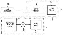
- FIG. 4 is a block diagram of a variable compensation circuit that permits generation of the compensation signal to start in advance of the duty cycle by a fixed small value in each switching cycle. With this circuit, the operating duty cycle is sensed and the slope compensation signal is started only slightly before the regulator switch turns off. The unnecessary slope compensation over lower duty cycles is avoided. Sleep mode level can be detected more accurately.
- the magnitude of the slope compensation signal at switching pulse termination is at a level that does not significantly lower the switch current limit level.
- Amplifier circuit 37 outputs a compensation signal Sx, having a constant slope, that may be coupled as an input to the adder 30 of FIG. 1 .
- Buffer amplifier 38 receives a ramp signal from ramp generator 48 .
- the ramp generator may comprise a well known capacitive circuit that is synchronized with a clock signal to provide a sawtooth type waveform having a constant slope.
- the buffer amplifier 38 receives a second signal from variable offset circuit 41 , which adds, via summer 40 , a fixed offset voltage from source 36 to a signal provided by duty cycle detection circuit 45 .
- the output of duty cycle detection circuit 45 is proportional to the regulator duty cycle.
- the output of the circuit 41 is proportional to the regulator duty cycle offset by the fixed level of the source 36 .
- the output circuit 39 initiates output signal Sx in each cycle when the ramp generator signal exceeds the signal received from variable offset circuit 41 .
- the output signal Sx commences later in a switching cycle for higher duty cycle operation than for lower duty cycle operation and is thus variable with respect to its phase in the switching cycle. There is fixed phase difference between Sx and the operating duty cycle.
- FIG. 5 is a partial circuit diagram of the variable compensation circuit of FIG. 4 .
- Transistor 32 is coupled in series with resistor 34 and adder 40 . These elements form, in part, the output circuit 39 that produces the compensation signal Sx.
- a first input of adder 40 is coupled to fixed offset voltage 36 .
- the second input of adder 40 is coupled to buffer 42 .
- the input of buffer 42 is coupled to a junction between resistor 44 and capacitor 46 .
- Buffer 42 , resistor 44 and capacitor 46 form the duty cycle detection circuit 45 .
- Voltage signal V 1 is coupled to resistor 44 .
- the positive input of amplifier 38 is coupled to receive a ramp signal Vramp.
- the negative input of amplifier 38 is coupled to the junction between transistor 32 and resistor 34 .
- the V 1 signal is a square signal that coincides with the regulator switching. As shown, V 1 is at a level of one volt for ninety percent of the cycle and at zero the last ten percent. This signal is averaged by the integrator formed by resistor 44 and capacitor 46 . The voltage at the junction of these two circuit elements thus is 0.9 volt at ninety percent duty cycle. This averaged voltage is buffered by buffer 42 and input to the adder 40 where it is added to the fixed voltage offset of voltage source 36 to provide a voltage Vx at the adder output. In this example, the fixed voltage offset has been selected at ⁇ 0.1 volt. Vx is thus 0.8 volt. Prior to conduction of transistor 32 , the voltages at both the transistor emitter and the negative input of amplifier 38 are at the level of Vx.
- the Vramp signal is generated at the start of each clock cycle and increases linearly until the next clock.
- the slope of this signal is selected such that its magnitude corresponds in number with the duty cycle. That is, for example, Vramp at 0.5 volt occurs at fifty percent duty cycle.
- amplifier 38 will drive transistor 32 to conduction.
- the voltage applied to the base of transistor 32 continues to increase and its conduction current, Sx, increases.
- the fixed offset voltage of source 36 has been chosen to be ⁇ 0.1 volt, whereby Vx becomes 0.8 volt.
- the compensation signal is initiated at eighty percent duty cycle, as illustrated in FIG. 6 a .
- the particular voltage offset selection has been made so that the slope compensation curve starts at only a small percent duty cycle ahead of the regulator operating duty cycle, ten percent in this example. If the duty cycle were to change to seventy percent, Vx would change to 0.6 volt and the compensation signal would commence at sixty percent duty cycle. When the transistor conducts, a voltage drop occurs across resistor 34 .
- the value of resistor 34 is selected to set a slope of Sx so that it is suitable for compensation without reaching a high level having the drawbacks of the prior art.
- the waveform diagram of FIG. 6 b is illustrative of the compensation signals produced by the prior art circuit of FIG. 2 and the circuit of FIG. 5 for ninety percent duty cycle operation, corresponding to the above described example.
- Compensation signal Sx 1 of the FIG. 2 circuit commences at fifty percent duty cycle and builds up to a high level at ninety percent duty cycle at which point switch cutoff occurs.
- the output current of adder 30 is equal to V C and comprises a large Sx 1 component.
- the Sx 1 component appears to be approximately eighty percent of the magnitude of the Vramp signal and a significantly large value in comparison with the V C level.
- compensation signal Sx 2 of the circuit of FIG. 5 commences at eighty percent duty cycle with the same slope.
- the Sx 2 component of the output of adder 30 appears to be approximately twenty percent of the magnitude of the Vramp signal.
- the accuracy of V C as an indicator of output load current and the switching current limit level are greatly improved.
Abstract
Description
Claims (12)
Priority Applications (4)
| Application Number | Priority Date | Filing Date | Title |
|---|---|---|---|
| US11/180,556 US7656142B2 (en) | 2005-07-14 | 2005-07-14 | Switching regulator with variable slope compensation |
| CN200580051311XA CN101238424B (en) | 2005-07-14 | 2005-09-08 | Switching regulator with variable slope compensation |
| PCT/US2005/032247 WO2007011371A1 (en) | 2005-07-14 | 2005-09-08 | Switching regulator with variable slope compensation |
| TW094131662A TWI361567B (en) | 2005-07-14 | 2005-09-14 | Switching regulator with variable slope compensation |
Applications Claiming Priority (1)
| Application Number | Priority Date | Filing Date | Title |
|---|---|---|---|
| US11/180,556 US7656142B2 (en) | 2005-07-14 | 2005-07-14 | Switching regulator with variable slope compensation |
Publications (2)
| Publication Number | Publication Date |
|---|---|
| US20070013355A1 US20070013355A1 (en) | 2007-01-18 |
| US7656142B2 true US7656142B2 (en) | 2010-02-02 |
Family
ID=35613744
Family Applications (1)
| Application Number | Title | Priority Date | Filing Date |
|---|---|---|---|
| US11/180,556 Active 2027-10-18 US7656142B2 (en) | 2005-07-14 | 2005-07-14 | Switching regulator with variable slope compensation |
Country Status (4)
| Country | Link |
|---|---|
| US (1) | US7656142B2 (en) |
| CN (1) | CN101238424B (en) |
| TW (1) | TWI361567B (en) |
| WO (1) | WO2007011371A1 (en) |
Cited By (6)
| Publication number | Priority date | Publication date | Assignee | Title |
|---|---|---|---|---|
| US20090122578A1 (en) * | 2007-11-08 | 2009-05-14 | Astec Custom Power (Hk) Ltd. | Duty Cycle Dependent Non-Linear Slope Compensation For Improved Dynamic Response |
| US20100019745A1 (en) * | 2008-07-22 | 2010-01-28 | Texas Instruments Incorporated | Multiple switch node power converter control scheme that avoids switching sub-harmonics |
| US20120074917A1 (en) * | 2010-04-02 | 2012-03-29 | Hsing-Kuo Chao | Adaptive slope-compensation module and method thereof |
| US8289010B1 (en) * | 2005-10-03 | 2012-10-16 | Zilker Labs, Inc. | Method for control of overlap times in switching power converters |
| WO2013009122A2 (en) * | 2011-07-14 | 2013-01-17 | (주)제퍼로직 | Switching mode power supply apparatus comprising tilt compensation circuit |
| US8860395B2 (en) | 2011-08-15 | 2014-10-14 | Analog Devices, Inc. | Circuit and method for generating a ramp compensation voltage for a switching regulator |
Families Citing this family (12)
| Publication number | Priority date | Publication date | Assignee | Title |
|---|---|---|---|---|
| US7042207B1 (en) * | 2003-11-07 | 2006-05-09 | National Semiconductor Corporation | Inductive measurement system and method |
| US7378822B2 (en) * | 2005-11-17 | 2008-05-27 | Linear Technology Corporation | Switching regulator slope compensation generator circuit |
| US8036762B1 (en) | 2007-05-09 | 2011-10-11 | Zilker Labs, Inc. | Adaptive compensation in digital power controllers |
| US8320144B2 (en) * | 2007-08-22 | 2012-11-27 | Silicon Mitus, Inc. | Power factor correction circuit for reducing distortion of input current |
| TWI415375B (en) * | 2008-12-22 | 2013-11-11 | Univ Nat Taiwan Science Tech | Modulation method and device of reduce duty cycle for a resonant converter |
| US8643355B2 (en) * | 2011-02-07 | 2014-02-04 | Semiconductor Components Industries, Llc | Method for generating a signal and structure therefor |
| US8686702B2 (en) * | 2012-02-15 | 2014-04-01 | Linear Technology Corporation | Negative slope compensation for current mode switching power supply |
| US9287779B2 (en) | 2013-03-14 | 2016-03-15 | Qualcomm Incorporated | Systems and methods for 100 percent duty cycle in switching regulators |
| FR3052935B1 (en) * | 2016-06-21 | 2020-08-28 | Thales Sa | STATIC BIAIS REDUCTION ENERGY CONVERTER INTRODUCED BY A STABILIZATION RAMP |
| US10243460B2 (en) * | 2017-02-28 | 2019-03-26 | Infineon Technologies Austria Ag | Method and apparatus for dynamic voltage transition control in semi-resonant and resonant converters |
| US11482928B2 (en) * | 2019-12-31 | 2022-10-25 | Dialog Semiconductor (Uk) Limited | Adaptive slope compensation |
| CN114189152B (en) * | 2021-08-16 | 2024-01-23 | 杰华特微电子股份有限公司 | Compensation control circuit and control method of switch type regulator and switch type regulator |
Citations (19)
| Publication number | Priority date | Publication date | Assignee | Title |
|---|---|---|---|---|
| US4399412A (en) * | 1981-12-21 | 1983-08-16 | Gte Automatic Electric Labs Inc. | Duty cycle monitor circuit |
| US4837495A (en) * | 1987-10-13 | 1989-06-06 | Astec U.S.A. (Hk) Limited | Current mode converter with controlled slope compensation |
| US4975820A (en) * | 1989-09-01 | 1990-12-04 | National Semiconductor Corporation | Adaptive compensating ramp generator for current-mode DC/DC converters |
| US5450036A (en) * | 1993-02-23 | 1995-09-12 | Rohm Co., Ltd. | Power amplifier circuit for audio signal and audio device using the same |
| US5523676A (en) * | 1994-03-31 | 1996-06-04 | Delco Electronics Corp. | Sample and hold method and apparatus for sensing inductive load current |
| US5861735A (en) * | 1997-02-27 | 1999-01-19 | Nec Corporation | Switching power supply circuit |
| US5903452A (en) | 1997-08-11 | 1999-05-11 | System General Corporation | Adaptive slope compensator for current mode power converters |
| US5929620A (en) * | 1996-11-07 | 1999-07-27 | Linear Technology Corporation | Switching regulators having a synchronizable oscillator frequency with constant ramp amplitude |
| US6320438B1 (en) * | 2000-08-17 | 2001-11-20 | Pericom Semiconductor Corp. | Duty-cycle correction driver with dual-filter feedback loop |
| US6351162B1 (en) * | 1999-05-03 | 2002-02-26 | Stmicroelectronics Gmbh | Circuit arrangement for controlling an inductive load |
| US6400232B1 (en) * | 2000-05-10 | 2002-06-04 | Delphi Technologies, Inc. | Variable duty cycle oscillator circuit with fixed minimum and maximum duty cycles |
| US6498466B1 (en) * | 2000-05-23 | 2002-12-24 | Linear Technology Corp. | Cancellation of slope compensation effect on current limit |
| US6522116B1 (en) * | 2000-07-17 | 2003-02-18 | Linear Technology Corporation | Slope compensation circuit utilizing CMOS linear effects |
| US20040095105A1 (en) * | 2002-11-18 | 2004-05-20 | Rohm Co., Ltd. | Power supply device and liquid crystal display device using the same |
| US6897640B2 (en) * | 2001-09-07 | 2005-05-24 | Stmicroelectronics S.A. | Switched mode power supply device adapted for low current drains, and cellular phone equipped with such a device |
| US7145375B2 (en) * | 2005-01-12 | 2006-12-05 | Infineon Technologies Ag | Duty cycle detector with first, second, and third values |
| US20060284607A1 (en) * | 2005-06-16 | 2006-12-21 | Yuji Isobe | Slope compensation circuit |
| US7176668B2 (en) * | 2004-07-08 | 2007-02-13 | Matsushita Electric Industrial Co., Ltd. | Switching regulator with advanced slope compensation |
| US7202640B2 (en) * | 2003-09-30 | 2007-04-10 | Sanken Electric Co., Ltd. | Power factor improving circuit |
-
2005
- 2005-07-14 US US11/180,556 patent/US7656142B2/en active Active
- 2005-09-08 WO PCT/US2005/032247 patent/WO2007011371A1/en active Application Filing
- 2005-09-08 CN CN200580051311XA patent/CN101238424B/en not_active Expired - Fee Related
- 2005-09-14 TW TW094131662A patent/TWI361567B/en not_active IP Right Cessation
Patent Citations (19)
| Publication number | Priority date | Publication date | Assignee | Title |
|---|---|---|---|---|
| US4399412A (en) * | 1981-12-21 | 1983-08-16 | Gte Automatic Electric Labs Inc. | Duty cycle monitor circuit |
| US4837495A (en) * | 1987-10-13 | 1989-06-06 | Astec U.S.A. (Hk) Limited | Current mode converter with controlled slope compensation |
| US4975820A (en) * | 1989-09-01 | 1990-12-04 | National Semiconductor Corporation | Adaptive compensating ramp generator for current-mode DC/DC converters |
| US5450036A (en) * | 1993-02-23 | 1995-09-12 | Rohm Co., Ltd. | Power amplifier circuit for audio signal and audio device using the same |
| US5523676A (en) * | 1994-03-31 | 1996-06-04 | Delco Electronics Corp. | Sample and hold method and apparatus for sensing inductive load current |
| US5929620A (en) * | 1996-11-07 | 1999-07-27 | Linear Technology Corporation | Switching regulators having a synchronizable oscillator frequency with constant ramp amplitude |
| US5861735A (en) * | 1997-02-27 | 1999-01-19 | Nec Corporation | Switching power supply circuit |
| US5903452A (en) | 1997-08-11 | 1999-05-11 | System General Corporation | Adaptive slope compensator for current mode power converters |
| US6351162B1 (en) * | 1999-05-03 | 2002-02-26 | Stmicroelectronics Gmbh | Circuit arrangement for controlling an inductive load |
| US6400232B1 (en) * | 2000-05-10 | 2002-06-04 | Delphi Technologies, Inc. | Variable duty cycle oscillator circuit with fixed minimum and maximum duty cycles |
| US6498466B1 (en) * | 2000-05-23 | 2002-12-24 | Linear Technology Corp. | Cancellation of slope compensation effect on current limit |
| US6522116B1 (en) * | 2000-07-17 | 2003-02-18 | Linear Technology Corporation | Slope compensation circuit utilizing CMOS linear effects |
| US6320438B1 (en) * | 2000-08-17 | 2001-11-20 | Pericom Semiconductor Corp. | Duty-cycle correction driver with dual-filter feedback loop |
| US6897640B2 (en) * | 2001-09-07 | 2005-05-24 | Stmicroelectronics S.A. | Switched mode power supply device adapted for low current drains, and cellular phone equipped with such a device |
| US20040095105A1 (en) * | 2002-11-18 | 2004-05-20 | Rohm Co., Ltd. | Power supply device and liquid crystal display device using the same |
| US7202640B2 (en) * | 2003-09-30 | 2007-04-10 | Sanken Electric Co., Ltd. | Power factor improving circuit |
| US7176668B2 (en) * | 2004-07-08 | 2007-02-13 | Matsushita Electric Industrial Co., Ltd. | Switching regulator with advanced slope compensation |
| US7145375B2 (en) * | 2005-01-12 | 2006-12-05 | Infineon Technologies Ag | Duty cycle detector with first, second, and third values |
| US20060284607A1 (en) * | 2005-06-16 | 2006-12-21 | Yuji Isobe | Slope compensation circuit |
Non-Patent Citations (3)
| Title |
|---|
| Holland, Barney. "Modelling, Analysis and Compensation of the Current-Mode Converter." Proceedings of Powercon. Annual International Power Electronics Conference, 1984, pp. 1-6, XP001057745. |
| Mac Lean, David, N. "A simplified Current Mode Control Model with Optimum Slope Compensation." Proceedings of the Intersociety Energy Conversion Engineering Conference, vol. 2, Aug. 12, 1990, pp. 37-42, XP010301332. |
| Sakurai, Hiroki. "Analysis and Design of a Current-Mode PWM Buck Converter Adopting the Output-Voltage Independent Second-Order Slope Compensation Scheme." IEICE Transactions Fundamentals of Electronics, Communications and Computer Sciences, Engineering Science Society, vol. E88-A, No. 2, Feb. 2005, pp. 490-497, XP001224568, ISSN: 0916-8508. |
Cited By (11)
| Publication number | Priority date | Publication date | Assignee | Title |
|---|---|---|---|---|
| US8289010B1 (en) * | 2005-10-03 | 2012-10-16 | Zilker Labs, Inc. | Method for control of overlap times in switching power converters |
| US20090122578A1 (en) * | 2007-11-08 | 2009-05-14 | Astec Custom Power (Hk) Ltd. | Duty Cycle Dependent Non-Linear Slope Compensation For Improved Dynamic Response |
| US8004253B2 (en) * | 2007-11-08 | 2011-08-23 | Astec International Limited | Duty cycle dependent non-linear slope compensation for improved dynamic response |
| US20100019745A1 (en) * | 2008-07-22 | 2010-01-28 | Texas Instruments Incorporated | Multiple switch node power converter control scheme that avoids switching sub-harmonics |
| US7902807B2 (en) * | 2008-07-22 | 2011-03-08 | Texas Instruments Incorporated | Multiple switch node power converter control scheme that avoids switching sub-harmonics |
| US20120074917A1 (en) * | 2010-04-02 | 2012-03-29 | Hsing-Kuo Chao | Adaptive slope-compensation module and method thereof |
| US8797013B2 (en) * | 2010-04-02 | 2014-08-05 | Leadtrend Technology Corp. | Adaptive slope-compensation module and method thereof |
| TWI460970B (en) * | 2010-04-02 | 2014-11-11 | Leadtrend Tech Corp | Adaptive slope-compensation module and method thereof |
| WO2013009122A2 (en) * | 2011-07-14 | 2013-01-17 | (주)제퍼로직 | Switching mode power supply apparatus comprising tilt compensation circuit |
| WO2013009122A3 (en) * | 2011-07-14 | 2013-04-11 | (주)제퍼로직 | Switching mode power supply apparatus comprising tilt compensation circuit |
| US8860395B2 (en) | 2011-08-15 | 2014-10-14 | Analog Devices, Inc. | Circuit and method for generating a ramp compensation voltage for a switching regulator |
Also Published As
| Publication number | Publication date |
|---|---|
| TW200703912A (en) | 2007-01-16 |
| WO2007011371A1 (en) | 2007-01-25 |
| US20070013355A1 (en) | 2007-01-18 |
| CN101238424B (en) | 2011-11-16 |
| CN101238424A (en) | 2008-08-06 |
| TWI361567B (en) | 2012-04-01 |
Similar Documents
| Publication | Publication Date | Title |
|---|---|---|
| US7656142B2 (en) | Switching regulator with variable slope compensation | |
| US7342392B2 (en) | Switching regulator with slope compensation independent of changes in switching frequency | |
| US7180274B2 (en) | Switching voltage regulator operating without a discontinuous mode | |
| US7898825B2 (en) | Adaptive ramp compensation for current mode-DC-DC converters | |
| US7605574B2 (en) | Switching regulator circuits | |
| JP5163283B2 (en) | Power factor correction circuit | |
| US7759919B2 (en) | Switching converter with plural converter stages having calibrated current uptake | |
| US7642733B2 (en) | Driving circuit for light emitting device with compensation mechanism and driving method thereof | |
| US7489121B2 (en) | Compensation offset adjustment scheme for fast reference voltage transitioning | |
| US7723967B2 (en) | Step-up converter having an improved dynamic response | |
| US20090058383A1 (en) | Switching DC-DC converter with adaptive-minimum-on-time control and method of adaptively controlling minimum-on-time of a switching DC-DC converter | |
| US10734902B2 (en) | Control of four-switch, single inductor, non-inverting buck-boost converters | |
| US8344711B2 (en) | Power supply device, control circuit and method for controlling power supply device | |
| JP4630165B2 (en) | DC-DC converter | |
| US20160006352A1 (en) | Control circuit, switching power supply and control method | |
| EP2885861B1 (en) | A current-mode controller for step-down (buck) converter | |
| US11183930B2 (en) | Power-save mode pulse gating control for switching converter | |
| US20090001952A1 (en) | Apparatus and method for improving a transient response of a power converter | |
| JP2005528875A (en) | DC-DC converter | |
| JP2002112535A (en) | Switching power supply | |
| JP2008206238A (en) | Current detection circuit, and current mode switching regulator | |
| US9641071B2 (en) | Cuk based current source | |
| US20090267573A1 (en) | Power Supplies, Power Supply Controllers, And Power Supply Controlling Methods | |
| EP3468022A1 (en) | Switch-mode power converter | |
| CN115437440B (en) | Voltage regulator and compensation method thereof |
Legal Events
| Date | Code | Title | Description |
|---|---|---|---|
| AS | Assignment |
Owner name: LINEAR TECHNOLOGY CORPORATION,CALIFORNIA Free format text: ASSIGNMENT OF ASSIGNORS INTEREST;ASSIGNOR:LIAO, CHIAWEI;REEL/FRAME:016777/0170 Effective date: 20050712 Owner name: LINEAR TECHNOLOGY CORPORATION, CALIFORNIA Free format text: ASSIGNMENT OF ASSIGNORS INTEREST;ASSIGNOR:LIAO, CHIAWEI;REEL/FRAME:016777/0170 Effective date: 20050712 |
|
| STCF | Information on status: patent grant |
Free format text: PATENTED CASE |
|
| CC | Certificate of correction | ||
| FPAY | Fee payment |
Year of fee payment: 4 |
|
| FPAY | Fee payment |
Year of fee payment: 8 |
|
| MAFP | Maintenance fee payment |
Free format text: PAYMENT OF MAINTENANCE FEE, 12TH YEAR, LARGE ENTITY (ORIGINAL EVENT CODE: M1553); ENTITY STATUS OF PATENT OWNER: LARGE ENTITY Year of fee payment: 12 |
|
| AS | Assignment |
Owner name: ANALOG DEVICES INTERNATIONAL UNLIMITED COMPANY, IRELAND Free format text: CHANGE OF NAME;ASSIGNOR:LINEAR TECHNOLOGY LLC;REEL/FRAME:057423/0205 Effective date: 20181105 Owner name: LINEAR TECHNOLOGY LLC, CALIFORNIA Free format text: CHANGE OF NAME;ASSIGNOR:LINEAR TECHNOLOGY CORPORATION;REEL/FRAME:057421/0714 Effective date: 20170502 |