US7622987B1 - Pattern-based DC offset correction - Google Patents
Pattern-based DC offset correction Download PDFInfo
- Publication number
- US7622987B1 US7622987B1 US12/019,535 US1953508A US7622987B1 US 7622987 B1 US7622987 B1 US 7622987B1 US 1953508 A US1953508 A US 1953508A US 7622987 B1 US7622987 B1 US 7622987B1
- Authority
- US
- United States
- Prior art keywords
- gain stage
- state
- output
- run length
- correction
- Prior art date
- Legal status (The legal status is an assumption and is not a legal conclusion. Google has not performed a legal analysis and makes no representation as to the accuracy of the status listed.)
- Active, expires
Links
Images


Classifications
-
- H—ELECTRICITY
- H03—ELECTRONIC CIRCUITRY
- H03F—AMPLIFIERS
- H03F1/00—Details of amplifiers with only discharge tubes, only semiconductor devices or only unspecified devices as amplifying elements
- H03F1/32—Modifications of amplifiers to reduce non-linear distortion
-
- H—ELECTRICITY
- H03—ELECTRONIC CIRCUITRY
- H03F—AMPLIFIERS
- H03F2200/00—Indexing scheme relating to amplifiers
- H03F2200/375—Circuitry to compensate the offset being present in an amplifier
Definitions
- the invention generally relates to electronics.
- the invention relates to handling DC offsets in amplifiers.
- Typical analog amplifiers have a saturating input-output relationship, as illustrated in FIG. 1 .
- Linear signal processing typically uses operation in the linear part of the curve—at smaller inputs levels. Large input signals, or high-gain can result in output saturation. If the ac portion of the desired input signal is sufficiently small, but the dc portion is relatively large, then with sufficient gain, the output will be saturated.
- DC offset correction can be a relatively difficult problem to solve.
- DC offset correction is one of the most important problems facing the direct conversion radio, and the direct conversion radio is an efficient implementation of a radio.
- the invention can include, for example, a system configured to observe patterns in an output signal indicative of the presence of DC offsets.
- a system configured to observe patterns in an output signal indicative of the presence of DC offsets.
- an output of a gain stage can be sliced to +1s and ⁇ 1s, and the presence of a DC offset can result in relatively long run lengths of either +1s or ⁇ 1s.
- the relatively long run lengths are detected and corresponding corrections are made to reduce the run lengths, which typically reduces the DC offsets.
- FIG. 1 illustrates saturation in an amplifier
- FIG. 2 illustrates examples of sources for DC offsets in a direct conversion radio.
- FIG. 3 illustrates an example of an architecture for an amplifier according to one embodiment of the invention.
- FIG. 4 is a plot illustrating a relationship between run lengths and dc offsets.
- FIG. 5 illustrates an example of a single stage of an amplifier with DC offset correction.
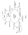
- FIG. 7 illustrates an example of a state machine representing a control algorithm that can be used, for example, in a gain stage of a plurality of gain stages.
- DC offset correction can be a relatively difficult problem to solve. Correction of DC offsets is desirable in many electronic environments, such as in direct conversion radios. Direct conversion radios and other analog signal processing circuits often use relatively high analog baseband gain. Signals processed by high-gain amplifiers typically do not contain useful content at DC. If spurious DC finds its way onto a signal, then the output of the high-gain amplifier can become saturated, thus distorting the desired part of the signal.
- DC offset correction is preferably performed in the “background” or during small duration “idle” times or slots.
- desired signal content is usually relatively close to DC so as to make the measurement of the undesired DC offset relatively difficult or time consuming with conventional linear analog or linear digital techniques.
- a closed feedback loop can be used to correct DC offset in an amplifier, but this approach would sense the DC offset present at the output of the amplifier. This can be done in an analog fashion with a low-pass filter, but this can create problems since the analog devices used to perform the low pass filter function in analog domain may be prohibitively large to create the relatively low cutoff frequency.
- the offset should be dynamically corrected, and the correction may need to be static during a particular duration of signal reception.
- a DC offset correction circuit operates relatively quickly during some defined time window. It is difficult to make an analog low pass filters that would meet those requirements. Furthermore, analog circuits can introduce uncertainty and other non-idealities.
- a problem of efficiently and quickly determining a DC offset can be encountered when a digital technique is used to correct the DC offset. It is preferred for the DC offset to be measured without the use of a high-resolution analog-to-digital converter (ADC), since processing of such signals is costly.
- ADC analog-to-digital converter
- FIG. 3 illustrates an example of an architecture for an amplifier according to one embodiment of the invention.
- the illustrated architecture includes a summing circuit 302 for compensation of the DC offset, a gain block 304 that amplifies an input signal to an output signal and possibly generates an undesirable DC offset to be corrected, a 1-bit slicer 306 , a pattern matching detector 308 , and a digital to analog converter (DAC) 310 .
- the summing circuit 302 , the 1-bit slicer 306 , the pattern matching detector 308 , and the DAC 310 form a correction circuit that corrects the DC offsets of the gain block 304 .
- the gain block 304 is typically implemented by an electronic circuit, such as by an integrated circuit of MOS devices.
- the summing circuit 302 and the gain block 304 are integrated as illustrated in FIG. 5 . Further details of the amplifier will be described in connection with FIGS. 4 and 5 .
- the illustrated embodiment of FIG. 3 has the following desirable features: (a) it is mostly digital, so uncertainty is reduced and variability from part to part is advantageously reduced over an analog implementation; (b) it does not require a high-resolution analog-to-digital converter (ADC), so the costly processing of wide-word signals is unnecessary; (c) the DC offset measurement is based on pattern matching, so it can be made to operate quickly in the presence of noise and other undesirable signals; and there is no latency due to the delay through an ADC.
- ADC analog-to-digital converter
- FIG. 4 is a plot illustrating a relationship between run lengths and DC offsets, which illustrates the principles behind the pattern detection.
- the pattern detection can be embodied in the pattern matching detector 308 , which can be implemented by hardware, by firmware/software or by a combination of both hardware and firmware/software.
- Firmware/software can be stored in a computer-readable medium. For example, a state diagram for detecting patterns and adjusting offset compensation will be described in greater detail later in connection with FIG. 7 .
- the run lengths of the output of the 1-bit slicer 306 are discussed. In telecommunications, slicing typically is typically used in conversion from soft symbols to hard symbols. However, since data bits are not being recovered by the 1-bit slicer 306 , the slicer does not have to convert actual symbols and can operate at a clock rate that is unrelated to a symbol rate. However, if the signal has a positive DC offset at the output of the 1-bit slicer 306 , the positive run lengths can be expected to exceed some threshold; if the signal has a negative DC offset at the output, the negative run lengths can be expected to exceed a threshold.
- Positive run lengths are defined as continuous unbroken runs of +1s (states of value +1) from the 1-bit slicer 306 .
- Negative run lengths are defined as continuous unbroken runs of ⁇ 1s (states of value ⁇ 1) from the 1-bit slicer 306 .
- FIG. 4 is a plot illustrating a relationship between run lengths and DC offsets that can be used to determine that DC offsets exist and to compensate for such DC offsets.
- An absolute value for DC offset is represented along the horizontal axis, with DC offset increasing to the right.
- a probability for a run length is represented along the vertical axis, with higher probability increasing to the top.
- the adaptive compensation algorithm is able to function on a IEEE 802.16d/e preamble, or during a transmit-receive (TXRX) gap when there is no receive signal, but noise and the presence of adjacent or alternate interferers can be expected, as well as in-band interferers from other subscribers.
- TXRX transmit-receive
- FIG. 5 illustrates an example of a single stage of an amplifier with DC offset correction.
- a gain block 502 includes an input for DC offset adjustment.
- the gain block 502 includes the summing circuit 302 and the gain block 304 described earlier in connection with FIG. 3 .
- other circuit topologies can be used to adjust DC offsets.
- FIG. 6 includes prophetic examples of corresponding waveforms for the amplifier illustrated in FIG. 5 .
- Time is represented along the horizontal axis and increases to the right.
- Various waveforms are represented along the vertical axis.
- Labels A, C, D, E on signal lines in FIG. 5 are represented by similarly labeled waveforms in FIG. 6 .
- Signal A and waveform A represent the input signal.
- Signal C and waveform C represent an output of the gain block 502 .
- Signal D and waveform D represent an output (sliced signal) of the 1-bit slicer 306 (clock reference for the 1-bit slicer 306 is not shown).
- the pattern matching detector 308 controls the output of the DAC 310 , such as, for example, by incrementing, decrementing, or maintaining a previous value that is provided as an input to the DAC 310 .
- the DAC 310 can also be configured to be incremented or decremented.
- the output of the DAC 310 provides an analog voltage for the compensation of DC offset voltages. It will be understood that an output of current instead of voltage can also be provided from the DAC 310 .
- the DC offset adjustment signal from the DAC 310 is labeled as signal E and waveform E.
- the input signal A has a DC offset that results in a relatively large DC offset that is represented in the waveform C.
- the run lengths are relatively long as expressed in waveform D.
- the relatively long run lengths are detected by the pattern matching detector 308 , by, for example, comparing the determined run lengths versus some threshold. Appropriate threshold values will be readily determined by one of ordinary skill in the art. It will be understood that the threshold values will typically vary based on the symbol rate of the 1-bit slicer 306 .
- the pattern matching detector 308 provides a control, such as a digital count, for the DAC 310 .
- the output E of the DAC 310 goes negative over time as illustrated by waveform C to correct or trim the DC offset, and output C of the gain block 502 has decreased DC offset as illustrated by the waveform C.
- Many amplifiers have more than one gain (amplifier) stage such as a series of gain stages arranged in a cascade.
- One or more gain stages can have their DC offsets adjusted.
- each of the gain stages of a series of gain stages is individually adjusted for DC offset correction.
- the state diagram of FIG. 7 can be used for a gain stage of a cascade of gain stages such that the DC offset correction for the gain stage can be coordinated with the DC offset corrections of other gain stages of the cascade of gain stages.
- the gain stages can correspond to variable gain amplifiers (VGAs).
- VGAs variable gain amplifiers
- two or more VGAs can be cascaded together, that is, arranged in series, for increased gain. It should be noted, however, that some of the gain stages can be non-variable gain.
- the illustrated architecture includes control signals labeled “my turn” and “your turn” which facilitate control.
- the signal “my turn” is an input signal for initiating the execution of the offset correction.
- the signal “your turn,” is an output signal that is asserted when the offset correction has been executed.
- a controller (not shown) can assert the “my turn” to a first VGA, wait for the first VGA to complete the offset correction, determine that offset correction is complete by monitoring the “your turn” signal, and then assert the “my turn” signal to the next VGA in the cascade of VGAs.
- the DC offset correction is also sequenced in the order of the signal flow, such as, for example, generally in the direction from input to output.
- the state diagram of FIG. 7 includes a standby state 702 , an update DAC state 704 , and a wait state 706 .
- the state diagram can describe the operation of a process or a state machine and can be used for control of an individual gain stage in a cascade of gain stages. While the state diagram of FIG. 7 will be described in the context of a state machine, it will be understood that portions of the state machine can be embodied in hardware, in firmware or software, or by a combination of both hardware and/or firmware/software. In addition, the illustrated state diagram can be modified in a variety of ways. For example, in another embodiment, various portions of the illustrated state diagram can be combined, can be divided, can be rearranged in an alternate sequence, can be removed, or the like.
- the state machine begins in the standby state 702 .
- the state machine monitors the run lengths and is responsive to patterns. For example, the state machine can monitor the output of the 1-bit slicer 306 ( FIGS. 3 and 5 ) to observe for patterns of run lengths of +1s or ⁇ 1s. In the illustrated state machine, the run lengths of +1s are counted as positive values, and the run lengths of ⁇ 1s are counted as negative values. The counts for run length are represented in the state diagram with the variable “runlength.” It will be understood that separate counts can alternatively be maintained for the +1 and the ⁇ 1 run length counts.
- the DC offset is decreased (more negative) by, for example, lowering the output voltage of the DAC 310 as indicated by “DAC ⁇ .”
- the state machine then proceeds to the wait state 706 , which permits the correction with time to become effective, before returning to the update DAC 704 state 704 .
- An appropriate time for the wait state 706 will be readily determined by one of ordinary skill in the art and will depend on factors such as slew rates and the like. If the count (negative “runlength”) is below the threshold ( ⁇ X) for the negative offset (exceeds the threshold in absolute value), then the DC offset is increased (more positive), by, for example, raising the output voltage of the DAC 310 as indicated by “DAC++.”
- the offset correction is complete until reinitiated, and the state machine can indicate to a controller that the DC offset correction is complete or can indicate to a subsequent gain stage that the subsequent gain stage can initiate its offset correction.
- the “your turn” control output of one gain stage is provided as the “my turn” control input of a subsequent gain stage.
- the state machine can return to the update DAC state 704 .
- the state machine returns to the standby state 702 .
- DACs have range and resolution limits.
- One embodiment examines the output or input for the DAC(s) and watches for an “idle tone,” that is, a sequence of DAC increments and decrements which indicate that the DAC resolution limit has been reached and no further offset corrections can be made. When such an idle tone is detected, the state machine can pass control to the next VGA DC offset correction sub-system.
- a pseudo-code description of an algorithm represented by the state diagram of FIG. 7 is presented in the following.
- the following pseudo-code illustrates how to compute the run lengths, and the integrated run length, or run length balance (note that the pseudo-code examines the current (time) output of the slicer (“slicer” variable), and the output of the slicer from the previous time (“last slicer” variable)):
- the DC offset DACs can be controlled as shown in the following pseudo-code:
- Patterns other than run lengths exceeding a simple threshold are possible.
- the threshold can be varied as a function of time, or as a function of previous run length values.
- the run lengths themselves can be filtered or averaged to estimate the DC offset, which can improve accuracy.
- One embodiment uses a threshold that can vary over time. For example, the threshold can be increased with time so that “false positive” DAC updates are avoided.
- One embodiment examines patterns of the run lengths themselves, such as an average value of run lengths (“rlBalance” in the pseudo-code) in a given run length sequence.
- One embodiment simultaneously examines the instantaneous run lengths and the integrated run lengths (as illustrated in the pseudo-code).
- One embodiment examines patterns of the run lengths themselves, looks for a preponderance of positive or negative run lengths, and adjusts the DACs accordingly. For example, if 8 of the last 10 run lengths have been positive, then the DAC should be decremented, even if the value of the run lengths have not exceeded the simple run length threshold.
- One embodiment includes control of a low gain mode for the variable gain amplifiers (VGAs) during adapt time in which the VGAs are set to a relatively low, such as minimum gain, which can reduce the impact of high transition density at the comparator input due to noise or other interferers.
- VGAs variable gain amplifiers
- One embodiment examines the elapsed time since a DAC updates update and passes control to the next VGA/DC offset correction block if the time exceeds a certain value.
- One embodiment examines the output of the DACs and watching for an “idle” tone, that is, a sequence of DAC increments and decrements which indicate that the DAC resolution limit has been reached and no further offset corrections can be made.
- an idle tone is detected, the algorithm can pass control to the next VGA DC offset correction sub-system.
- integration is performed by a pure integrator.
- the positive and negative values being integrated typically prevent the integrator from overflowing; however, a maximum value, such as a saturation value, can be used to limit the integrated value.
- a digital filter with a low-pass characteristic is used.
- One example of such a filter is a moving average.
- an exponentially-weighted moving average is used.
- a voting technique is used (such as 8 of the last 10).
Abstract
Description
-
- runLength=−1;
- rlBalance+=runLength;
-
- runLength=+1;
- rlBalance+=runLength;
Claims (23)
Priority Applications (1)
| Application Number | Priority Date | Filing Date | Title |
|---|---|---|---|
| US12/019,535 US7622987B1 (en) | 2007-01-25 | 2008-01-24 | Pattern-based DC offset correction |
Applications Claiming Priority (2)
| Application Number | Priority Date | Filing Date | Title |
|---|---|---|---|
| US88657607P | 2007-01-25 | 2007-01-25 | |
| US12/019,535 US7622987B1 (en) | 2007-01-25 | 2008-01-24 | Pattern-based DC offset correction |
Publications (1)
| Publication Number | Publication Date |
|---|---|
| US7622987B1 true US7622987B1 (en) | 2009-11-24 |
Family
ID=41327829
Family Applications (1)
| Application Number | Title | Priority Date | Filing Date |
|---|---|---|---|
| US12/019,535 Active 2028-02-20 US7622987B1 (en) | 2007-01-25 | 2008-01-24 | Pattern-based DC offset correction |
Country Status (1)
| Country | Link |
|---|---|
| US (1) | US7622987B1 (en) |
Cited By (3)
| Publication number | Priority date | Publication date | Assignee | Title |
|---|---|---|---|---|
| US8779952B1 (en) * | 2012-04-12 | 2014-07-15 | Pmc-Sierra Us, Inc. | Background calibration of threshold errors in analog to digital converters |
| US8810442B1 (en) | 2013-02-14 | 2014-08-19 | Pmc-Sierra Us, Inc. | Background calibration of aperture center errors in analog to digital converters |
| WO2015102431A1 (en) * | 2014-01-03 | 2015-07-09 | 삼성전자주식회사 | Method and apparatus for direct conversion receiver correcting direct current offset |
Citations (39)
| Publication number | Priority date | Publication date | Assignee | Title |
|---|---|---|---|---|
| US4490682A (en) * | 1981-12-15 | 1984-12-25 | Analogic Corporation | Instrumentation amplifier having automatic offset adjustment |
| US4581748A (en) | 1982-12-29 | 1986-04-08 | Fujitsu Limited | QAM with DC bias in one channel |
| US4633484A (en) | 1983-11-30 | 1986-12-30 | Fujitsu Limited | Receiver unit in radio communication system |
| US4862081A (en) | 1988-11-23 | 1989-08-29 | Picker International, Inc. | DC artifact removal in magnetic resonance imaging |
| US5140699A (en) | 1990-12-24 | 1992-08-18 | American Nucleonics Corporation | Detector DC offset compensator |
| US5212826A (en) | 1990-12-20 | 1993-05-18 | Motorola, Inc. | Apparatus and method of dc offset correction for a receiver |
| US5241702A (en) | 1990-09-06 | 1993-08-31 | Telefonaktiebolaget L M Ericsson | D.c. offset compensation in a radio receiver |
| US5263194A (en) | 1990-03-07 | 1993-11-16 | Seiko Corp. | Zero if radio receiver for intermittent operation |
| US5311554A (en) | 1992-07-02 | 1994-05-10 | Motorola, Inc. | Synchronized offset extraction in a data receiver |
| US5715281A (en) | 1995-02-21 | 1998-02-03 | Tait Electronics Limited | Zero intermediate frequency receiver |
| US5724653A (en) | 1994-12-20 | 1998-03-03 | Lucent Technologies Inc. | Radio receiver with DC offset correction circuit |
| US5903825A (en) | 1996-06-27 | 1999-05-11 | Motorola, Inc. | Digital FM receiver back end |
| US6006079A (en) | 1997-06-13 | 1999-12-21 | Motorola, Inc. | Radio having a fast adapting direct conversion receiver |
| US6035004A (en) | 1995-11-02 | 2000-03-07 | Mitsubishi Denki Kabushiki Kaisha | Digital radio receiver |
| US6075409A (en) | 1998-04-03 | 2000-06-13 | Motorola, Inc. | Demodulation method and arrangement |
| US6185260B1 (en) | 1997-05-30 | 2001-02-06 | Nec Corporation | Radio communication device using quadrature modulation-demodulation circuit |
| US6218787B1 (en) | 1998-04-20 | 2001-04-17 | Jrs Technology Inc. | Remote dimming control system for a fluorescent ballast utilizing existing building wiring |
| US6259748B1 (en) | 1996-12-31 | 2001-07-10 | Nokia Mobile Phones Limited | Signal offset elimination |
| US6335656B1 (en) | 1999-09-30 | 2002-01-01 | Analog Devices, Inc. | Direct conversion receivers and filters adapted for use therein |
| US6339711B1 (en) | 1997-03-14 | 2002-01-15 | Kabushiki Kaisha Toshiba | Radio apparatus |
| US6370205B1 (en) | 1999-07-02 | 2002-04-09 | Telefonaktiebolaget Lm Ericsson (Publ) | Method and apparatus for performing DC-offset compensation in a radio receiver |
| US6442380B1 (en) | 1999-12-22 | 2002-08-27 | U.S. Philips Corporation | Automatic gain control in a zero intermediate frequency radio device |
| US6449320B1 (en) | 1999-07-02 | 2002-09-10 | Telefonaktiebolaget Lm Ericsson (Publ) | Equalization with DC-offset compensation |
| US6535725B2 (en) | 2001-03-30 | 2003-03-18 | Skyworks Solutions, Inc. | Interference reduction for direct conversion receivers |
| US6560447B2 (en) | 2001-03-05 | 2003-05-06 | Motorola, Inc. | DC offset correction scheme for wireless receivers |
| US6560448B1 (en) | 2000-10-02 | 2003-05-06 | Intersil Americas Inc. | DC compensation system for a wireless communication device configured in a zero intermediate frequency architecture |
| US6725024B1 (en) | 2000-11-07 | 2004-04-20 | Telefonaktiebolaget Lm Ericsson (Publ) | Offset local oscillator frequency |
| US6753727B2 (en) * | 2002-06-13 | 2004-06-22 | Skyworks Solutions, Inc. | Sequential DC offset correction for amplifier chain |
| US6757340B1 (en) | 1999-02-22 | 2004-06-29 | Telefonaktiebolaget L M Ericsson (Publ) | Radio receiver and method for preloading an average DC-offset into a channel filter |
| US6897700B1 (en) * | 2003-03-21 | 2005-05-24 | Applied Micro Circuits Corporation | Amplifier with digital DC offset cancellation feature |
| US6922161B2 (en) | 2003-01-03 | 2005-07-26 | Samsung Electronics Co., Ltd. | Delta-Sigma modulator for reducing quantization noise and oversampling ratio (OSR) |
| US6937847B2 (en) | 2002-10-30 | 2005-08-30 | Advanced Micro Devices, Inc. | Integrated RF signal level detector usable for automatic power level control |
| US6975848B2 (en) | 2002-06-04 | 2005-12-13 | Parkervision, Inc. | Method and apparatus for DC offset removal in a radio frequency communication channel |
| US6995595B2 (en) | 2002-08-05 | 2006-02-07 | Samsung Electronics Co., Ltd. | Direct conversion receiver having a DC offset eliminating function |
| US6999537B2 (en) | 2002-10-25 | 2006-02-14 | Qualcomm Incorporated | Method of removing DC offset for a ZIF-based GSM radio solution with digital frequency correlation |
| US7020449B2 (en) | 2002-10-21 | 2006-03-28 | Broadcom Corporation | Fast settling variable gain amplifier with DC offset cancellation |
| US7024221B2 (en) | 2001-01-12 | 2006-04-04 | Silicon Laboratories Inc. | Notch filter for DC offset reduction in radio-frequency apparatus and associated methods |
| US7039382B2 (en) | 2001-05-15 | 2006-05-02 | Broadcom Corporation | DC offset calibration for a radio transceiver mixer |
| US7046720B2 (en) | 2001-11-12 | 2006-05-16 | Telefonktiebolaget Lm Ericsson (Publ) | System and method for DC offset compensation in a WCDMA receiver |
-
2008
- 2008-01-24 US US12/019,535 patent/US7622987B1/en active Active
Patent Citations (41)
| Publication number | Priority date | Publication date | Assignee | Title |
|---|---|---|---|---|
| US4490682A (en) * | 1981-12-15 | 1984-12-25 | Analogic Corporation | Instrumentation amplifier having automatic offset adjustment |
| US4581748A (en) | 1982-12-29 | 1986-04-08 | Fujitsu Limited | QAM with DC bias in one channel |
| US4633484A (en) | 1983-11-30 | 1986-12-30 | Fujitsu Limited | Receiver unit in radio communication system |
| US4862081A (en) | 1988-11-23 | 1989-08-29 | Picker International, Inc. | DC artifact removal in magnetic resonance imaging |
| US5263194A (en) | 1990-03-07 | 1993-11-16 | Seiko Corp. | Zero if radio receiver for intermittent operation |
| US5241702A (en) | 1990-09-06 | 1993-08-31 | Telefonaktiebolaget L M Ericsson | D.c. offset compensation in a radio receiver |
| US5212826A (en) | 1990-12-20 | 1993-05-18 | Motorola, Inc. | Apparatus and method of dc offset correction for a receiver |
| US5140699A (en) | 1990-12-24 | 1992-08-18 | American Nucleonics Corporation | Detector DC offset compensator |
| US5311554A (en) | 1992-07-02 | 1994-05-10 | Motorola, Inc. | Synchronized offset extraction in a data receiver |
| US5724653A (en) | 1994-12-20 | 1998-03-03 | Lucent Technologies Inc. | Radio receiver with DC offset correction circuit |
| US5715281A (en) | 1995-02-21 | 1998-02-03 | Tait Electronics Limited | Zero intermediate frequency receiver |
| US6035004A (en) | 1995-11-02 | 2000-03-07 | Mitsubishi Denki Kabushiki Kaisha | Digital radio receiver |
| US5903825A (en) | 1996-06-27 | 1999-05-11 | Motorola, Inc. | Digital FM receiver back end |
| US6259748B1 (en) | 1996-12-31 | 2001-07-10 | Nokia Mobile Phones Limited | Signal offset elimination |
| US6816712B2 (en) | 1997-03-14 | 2004-11-09 | Kabushiki Kaisha Toshiba | Radio apparatus |
| US6339711B1 (en) | 1997-03-14 | 2002-01-15 | Kabushiki Kaisha Toshiba | Radio apparatus |
| US6185260B1 (en) | 1997-05-30 | 2001-02-06 | Nec Corporation | Radio communication device using quadrature modulation-demodulation circuit |
| US6006079A (en) | 1997-06-13 | 1999-12-21 | Motorola, Inc. | Radio having a fast adapting direct conversion receiver |
| US6075409A (en) | 1998-04-03 | 2000-06-13 | Motorola, Inc. | Demodulation method and arrangement |
| US6218787B1 (en) | 1998-04-20 | 2001-04-17 | Jrs Technology Inc. | Remote dimming control system for a fluorescent ballast utilizing existing building wiring |
| US6757340B1 (en) | 1999-02-22 | 2004-06-29 | Telefonaktiebolaget L M Ericsson (Publ) | Radio receiver and method for preloading an average DC-offset into a channel filter |
| US6370205B1 (en) | 1999-07-02 | 2002-04-09 | Telefonaktiebolaget Lm Ericsson (Publ) | Method and apparatus for performing DC-offset compensation in a radio receiver |
| US6449320B1 (en) | 1999-07-02 | 2002-09-10 | Telefonaktiebolaget Lm Ericsson (Publ) | Equalization with DC-offset compensation |
| US6335656B1 (en) | 1999-09-30 | 2002-01-01 | Analog Devices, Inc. | Direct conversion receivers and filters adapted for use therein |
| US6442380B1 (en) | 1999-12-22 | 2002-08-27 | U.S. Philips Corporation | Automatic gain control in a zero intermediate frequency radio device |
| US6560448B1 (en) | 2000-10-02 | 2003-05-06 | Intersil Americas Inc. | DC compensation system for a wireless communication device configured in a zero intermediate frequency architecture |
| US6725024B1 (en) | 2000-11-07 | 2004-04-20 | Telefonaktiebolaget Lm Ericsson (Publ) | Offset local oscillator frequency |
| US7024221B2 (en) | 2001-01-12 | 2006-04-04 | Silicon Laboratories Inc. | Notch filter for DC offset reduction in radio-frequency apparatus and associated methods |
| US6560447B2 (en) | 2001-03-05 | 2003-05-06 | Motorola, Inc. | DC offset correction scheme for wireless receivers |
| US6535725B2 (en) | 2001-03-30 | 2003-03-18 | Skyworks Solutions, Inc. | Interference reduction for direct conversion receivers |
| US7039382B2 (en) | 2001-05-15 | 2006-05-02 | Broadcom Corporation | DC offset calibration for a radio transceiver mixer |
| US7046720B2 (en) | 2001-11-12 | 2006-05-16 | Telefonktiebolaget Lm Ericsson (Publ) | System and method for DC offset compensation in a WCDMA receiver |
| US6975848B2 (en) | 2002-06-04 | 2005-12-13 | Parkervision, Inc. | Method and apparatus for DC offset removal in a radio frequency communication channel |
| US6753727B2 (en) * | 2002-06-13 | 2004-06-22 | Skyworks Solutions, Inc. | Sequential DC offset correction for amplifier chain |
| US6995595B2 (en) | 2002-08-05 | 2006-02-07 | Samsung Electronics Co., Ltd. | Direct conversion receiver having a DC offset eliminating function |
| US7020449B2 (en) | 2002-10-21 | 2006-03-28 | Broadcom Corporation | Fast settling variable gain amplifier with DC offset cancellation |
| US6999537B2 (en) | 2002-10-25 | 2006-02-14 | Qualcomm Incorporated | Method of removing DC offset for a ZIF-based GSM radio solution with digital frequency correlation |
| US6937847B2 (en) | 2002-10-30 | 2005-08-30 | Advanced Micro Devices, Inc. | Integrated RF signal level detector usable for automatic power level control |
| US6922161B2 (en) | 2003-01-03 | 2005-07-26 | Samsung Electronics Co., Ltd. | Delta-Sigma modulator for reducing quantization noise and oversampling ratio (OSR) |
| US6897700B1 (en) * | 2003-03-21 | 2005-05-24 | Applied Micro Circuits Corporation | Amplifier with digital DC offset cancellation feature |
| US7132861B1 (en) * | 2003-03-21 | 2006-11-07 | Applied Microcircuits Corporation | Amplifier with digital DC offset cancellation feature |
Cited By (6)
| Publication number | Priority date | Publication date | Assignee | Title |
|---|---|---|---|---|
| US8779952B1 (en) * | 2012-04-12 | 2014-07-15 | Pmc-Sierra Us, Inc. | Background calibration of threshold errors in analog to digital converters |
| US8810442B1 (en) | 2013-02-14 | 2014-08-19 | Pmc-Sierra Us, Inc. | Background calibration of aperture center errors in analog to digital converters |
| US8952835B1 (en) | 2013-02-14 | 2015-02-10 | Pmc-Sierra Us, Inc. | Background calibration of aperture center errors in analog to digital converters |
| WO2015102431A1 (en) * | 2014-01-03 | 2015-07-09 | 삼성전자주식회사 | Method and apparatus for direct conversion receiver correcting direct current offset |
| US20160330049A1 (en) * | 2014-01-03 | 2016-11-10 | Samsung Electronics Co., Ltd. | Method and apparatus for direct conversion receiver correcting direct current offset |
| US9948484B2 (en) * | 2014-01-03 | 2018-04-17 | Samsung Electronics Co., Ltd. | Method and apparatus for direct conversion receiver correcting direct current offset |
Similar Documents
| Publication | Publication Date | Title |
|---|---|---|
| US6225848B1 (en) | Method and apparatus for settling and maintaining a DC offset | |
| US8744392B2 (en) | Automatic gain control circuit and automatic gain control method | |
| US6668027B1 (en) | Self adjusting automatic gain control (AGC) power reference level circuit | |
| US8295396B2 (en) | System and method for power control in a wireless transmitter | |
| US7426376B2 (en) | Receiver having digital automatic gain control | |
| US7203476B2 (en) | Method and apparatus for minimizing baseband offset error in a receiver | |
| US20100075624A1 (en) | Dc-offset-correction system and method for communication receivers | |
| JP4399447B2 (en) | OFDM receiver | |
| US8380149B2 (en) | DC offset canceller, receiving apparatus and DC offset cancellation method | |
| US7680473B2 (en) | Circuits and methods for signal gain control | |
| US7622987B1 (en) | Pattern-based DC offset correction | |
| US8165250B2 (en) | Automatic gain control device, signal receiving apparatus, and signal receiving method | |
| US20040185810A1 (en) | Automatic gain controller | |
| US9059671B2 (en) | Automatic gain control device | |
| US9025705B2 (en) | Current reduction in digital circuits | |
| US20180041235A1 (en) | EHF Receiver Architecture with Dynamically Adjustable Discrimination Threshold | |
| US7184729B2 (en) | Digital automatic gain control for transceiver devices | |
| US7643803B2 (en) | Power estimation of a transmission | |
| US7239199B1 (en) | Amplifier calibration | |
| JP2002164799A (en) | Method and device for controlling transmission power and communication apparatus | |
| MXPA02002628A (en) | Hdtv receiver having fast digital if agc and analog rf agc. | |
| JP2006524939A (en) | Amplification adjustment method and circuit | |
| US6664840B2 (en) | Offset calibration system and method for a high gain signal channel | |
| US8112052B2 (en) | Automatic gain control loop with hysteresis switching | |
| US20160211819A1 (en) | Receiver circuit and gain controlling method thereof |
Legal Events
| Date | Code | Title | Description |
|---|---|---|---|
| AS | Assignment |
Owner name: PMC-SIERRA, INC., CALIFORNIA Free format text: ASSIGNMENT OF ASSIGNORS INTEREST;ASSIGNOR:ZORTEA, ANTHONY EUGENE;REEL/FRAME:020420/0457 Effective date: 20080124 |
|
| STCF | Information on status: patent grant |
Free format text: PATENTED CASE |
|
| FPAY | Fee payment |
Year of fee payment: 4 |
|
| AS | Assignment |
Owner name: BANK OF AMERICA, N.A., NORTH CAROLINA Free format text: SECURITY INTEREST IN PATENTS;ASSIGNORS:PMC-SIERRA, INC.;PMC-SIERRA US, INC.;WINTEGRA, INC.;REEL/FRAME:030947/0710 Effective date: 20130802 |
|
| AS | Assignment |
Owner name: PMC-SIERRA, INC., CALIFORNIA Free format text: RELEASE BY SECURED PARTY;ASSIGNOR:BANK OF AMERICA, N.A.;REEL/FRAME:037675/0129 Effective date: 20160115 Owner name: PMC-SIERRA US, INC., CALIFORNIA Free format text: RELEASE BY SECURED PARTY;ASSIGNOR:BANK OF AMERICA, N.A.;REEL/FRAME:037675/0129 Effective date: 20160115 Owner name: WINTEGRA, INC., CALIFORNIA Free format text: RELEASE BY SECURED PARTY;ASSIGNOR:BANK OF AMERICA, N.A.;REEL/FRAME:037675/0129 Effective date: 20160115 |
|
| AS | Assignment |
Owner name: MORGAN STANLEY SENIOR FUNDING, INC., NEW YORK Free format text: PATENT SECURITY AGREEMENT;ASSIGNORS:MICROSEMI STORAGE SOLUTIONS, INC. (F/K/A PMC-SIERRA, INC.);MICROSEMI STORAGE SOLUTIONS (U.S.), INC. (F/K/A PMC-SIERRA US, INC.);REEL/FRAME:037689/0719 Effective date: 20160115 |
|
| AS | Assignment |
Owner name: MICROSEMI STORAGE SOLUTIONS, INC., CALIFORNIA Free format text: CHANGE OF NAME;ASSIGNOR:PMC-SIERRA, INC.;REEL/FRAME:038381/0753 Effective date: 20160115 |
|
| FPAY | Fee payment |
Year of fee payment: 8 |
|
| AS | Assignment |
Owner name: MICROSEMI STORAGE SOLUTIONS, INC., CALIFORNIA Free format text: RELEASE BY SECURED PARTY;ASSIGNOR:MORGAN STANLEY SENIOR FUNDING, INC.;REEL/FRAME:046251/0271 Effective date: 20180529 Owner name: MICROSEMI STORAGE SOLUTIONS (U.S.), INC., CALIFORN Free format text: RELEASE BY SECURED PARTY;ASSIGNOR:MORGAN STANLEY SENIOR FUNDING, INC.;REEL/FRAME:046251/0271 Effective date: 20180529 |
|
| AS | Assignment |
Owner name: JPMORGAN CHASE BANK, N.A., AS ADMINISTRATIVE AGENT, ILLINOIS Free format text: SECURITY INTEREST;ASSIGNORS:MICROCHIP TECHNOLOGY INCORPORATED;SILICON STORAGE TECHNOLOGY, INC.;ATMEL CORPORATION;AND OTHERS;REEL/FRAME:046426/0001 Effective date: 20180529 Owner name: JPMORGAN CHASE BANK, N.A., AS ADMINISTRATIVE AGENT Free format text: SECURITY INTEREST;ASSIGNORS:MICROCHIP TECHNOLOGY INCORPORATED;SILICON STORAGE TECHNOLOGY, INC.;ATMEL CORPORATION;AND OTHERS;REEL/FRAME:046426/0001 Effective date: 20180529 |
|
| AS | Assignment |
Owner name: WELLS FARGO BANK, NATIONAL ASSOCIATION, AS NOTES COLLATERAL AGENT, CALIFORNIA Free format text: SECURITY INTEREST;ASSIGNORS:MICROCHIP TECHNOLOGY INCORPORATED;SILICON STORAGE TECHNOLOGY, INC.;ATMEL CORPORATION;AND OTHERS;REEL/FRAME:047103/0206 Effective date: 20180914 Owner name: WELLS FARGO BANK, NATIONAL ASSOCIATION, AS NOTES C Free format text: SECURITY INTEREST;ASSIGNORS:MICROCHIP TECHNOLOGY INCORPORATED;SILICON STORAGE TECHNOLOGY, INC.;ATMEL CORPORATION;AND OTHERS;REEL/FRAME:047103/0206 Effective date: 20180914 |
|
| AS | Assignment |
Owner name: JPMORGAN CHASE BANK, N.A., AS ADMINISTRATIVE AGENT, DELAWARE Free format text: SECURITY INTEREST;ASSIGNORS:MICROCHIP TECHNOLOGY INC.;SILICON STORAGE TECHNOLOGY, INC.;ATMEL CORPORATION;AND OTHERS;REEL/FRAME:053311/0305 Effective date: 20200327 |
|
| AS | Assignment |
Owner name: MICROCHIP TECHNOLOGY INC., ARIZONA Free format text: RELEASE BY SECURED PARTY;ASSIGNOR:JPMORGAN CHASE BANK, N.A, AS ADMINISTRATIVE AGENT;REEL/FRAME:053466/0011 Effective date: 20200529 Owner name: ATMEL CORPORATION, ARIZONA Free format text: RELEASE BY SECURED PARTY;ASSIGNOR:JPMORGAN CHASE BANK, N.A, AS ADMINISTRATIVE AGENT;REEL/FRAME:053466/0011 Effective date: 20200529 Owner name: MICROSEMI STORAGE SOLUTIONS, INC., ARIZONA Free format text: RELEASE BY SECURED PARTY;ASSIGNOR:JPMORGAN CHASE BANK, N.A, AS ADMINISTRATIVE AGENT;REEL/FRAME:053466/0011 Effective date: 20200529 Owner name: SILICON STORAGE TECHNOLOGY, INC., ARIZONA Free format text: RELEASE BY SECURED PARTY;ASSIGNOR:JPMORGAN CHASE BANK, N.A, AS ADMINISTRATIVE AGENT;REEL/FRAME:053466/0011 Effective date: 20200529 Owner name: MICROSEMI CORPORATION, CALIFORNIA Free format text: RELEASE BY SECURED PARTY;ASSIGNOR:JPMORGAN CHASE BANK, N.A, AS ADMINISTRATIVE AGENT;REEL/FRAME:053466/0011 Effective date: 20200529 |
|
| AS | Assignment |
Owner name: WELLS FARGO BANK, NATIONAL ASSOCIATION, MINNESOTA Free format text: SECURITY INTEREST;ASSIGNORS:MICROCHIP TECHNOLOGY INC.;SILICON STORAGE TECHNOLOGY, INC.;ATMEL CORPORATION;AND OTHERS;REEL/FRAME:053468/0705 Effective date: 20200529 |
|
| AS | Assignment |
Owner name: WELLS FARGO BANK, NATIONAL ASSOCIATION, AS COLLATERAL AGENT, MINNESOTA Free format text: SECURITY INTEREST;ASSIGNORS:MICROCHIP TECHNOLOGY INCORPORATED;SILICON STORAGE TECHNOLOGY, INC.;ATMEL CORPORATION;AND OTHERS;REEL/FRAME:055671/0612 Effective date: 20201217 |
|
| MAFP | Maintenance fee payment |
Free format text: PAYMENT OF MAINTENANCE FEE, 12TH YEAR, LARGE ENTITY (ORIGINAL EVENT CODE: M1553); ENTITY STATUS OF PATENT OWNER: LARGE ENTITY Year of fee payment: 12 |
|
| AS | Assignment |
Owner name: WELLS FARGO BANK, NATIONAL ASSOCIATION, AS NOTES COLLATERAL AGENT, MINNESOTA Free format text: SECURITY INTEREST;ASSIGNORS:MICROCHIP TECHNOLOGY INCORPORATED;SILICON STORAGE TECHNOLOGY, INC.;ATMEL CORPORATION;AND OTHERS;REEL/FRAME:057935/0474 Effective date: 20210528 |
|
| AS | Assignment |
Owner name: MICROSEMI STORAGE SOLUTIONS, INC., ARIZONA Free format text: RELEASE BY SECURED PARTY;ASSIGNOR:JPMORGAN CHASE BANK, N.A., AS ADMINISTRATIVE AGENT;REEL/FRAME:059333/0222 Effective date: 20220218 Owner name: MICROSEMI CORPORATION, ARIZONA Free format text: RELEASE BY SECURED PARTY;ASSIGNOR:JPMORGAN CHASE BANK, N.A., AS ADMINISTRATIVE AGENT;REEL/FRAME:059333/0222 Effective date: 20220218 Owner name: ATMEL CORPORATION, ARIZONA Free format text: RELEASE BY SECURED PARTY;ASSIGNOR:JPMORGAN CHASE BANK, N.A., AS ADMINISTRATIVE AGENT;REEL/FRAME:059333/0222 Effective date: 20220218 Owner name: SILICON STORAGE TECHNOLOGY, INC., ARIZONA Free format text: RELEASE BY SECURED PARTY;ASSIGNOR:JPMORGAN CHASE BANK, N.A., AS ADMINISTRATIVE AGENT;REEL/FRAME:059333/0222 Effective date: 20220218 Owner name: MICROCHIP TECHNOLOGY INCORPORATED, ARIZONA Free format text: RELEASE BY SECURED PARTY;ASSIGNOR:JPMORGAN CHASE BANK, N.A., AS ADMINISTRATIVE AGENT;REEL/FRAME:059333/0222 Effective date: 20220218 |
|
| AS | Assignment |
Owner name: MICROSEMI STORAGE SOLUTIONS, INC., ARIZONA Free format text: RELEASE BY SECURED PARTY;ASSIGNOR:WELLS FARGO BANK, NATIONAL ASSOCIATION, AS NOTES COLLATERAL AGENT;REEL/FRAME:059358/0001 Effective date: 20220228 Owner name: MICROSEMI CORPORATION, ARIZONA Free format text: RELEASE BY SECURED PARTY;ASSIGNOR:WELLS FARGO BANK, NATIONAL ASSOCIATION, AS NOTES COLLATERAL AGENT;REEL/FRAME:059358/0001 Effective date: 20220228 Owner name: ATMEL CORPORATION, ARIZONA Free format text: RELEASE BY SECURED PARTY;ASSIGNOR:WELLS FARGO BANK, NATIONAL ASSOCIATION, AS NOTES COLLATERAL AGENT;REEL/FRAME:059358/0001 Effective date: 20220228 Owner name: SILICON STORAGE TECHNOLOGY, INC., ARIZONA Free format text: RELEASE BY SECURED PARTY;ASSIGNOR:WELLS FARGO BANK, NATIONAL ASSOCIATION, AS NOTES COLLATERAL AGENT;REEL/FRAME:059358/0001 Effective date: 20220228 Owner name: MICROCHIP TECHNOLOGY INCORPORATED, ARIZONA Free format text: RELEASE BY SECURED PARTY;ASSIGNOR:WELLS FARGO BANK, NATIONAL ASSOCIATION, AS NOTES COLLATERAL AGENT;REEL/FRAME:059358/0001 Effective date: 20220228 |
|
| AS | Assignment |
Owner name: MICROSEMI STORAGE SOLUTIONS, INC., ARIZONA Free format text: RELEASE BY SECURED PARTY;ASSIGNOR:WELLS FARGO BANK, NATIONAL ASSOCIATION, AS NOTES COLLATERAL AGENT;REEL/FRAME:059863/0400 Effective date: 20220228 Owner name: MICROSEMI CORPORATION, ARIZONA Free format text: RELEASE BY SECURED PARTY;ASSIGNOR:WELLS FARGO BANK, NATIONAL ASSOCIATION, AS NOTES COLLATERAL AGENT;REEL/FRAME:059863/0400 Effective date: 20220228 Owner name: ATMEL CORPORATION, ARIZONA Free format text: RELEASE BY SECURED PARTY;ASSIGNOR:WELLS FARGO BANK, NATIONAL ASSOCIATION, AS NOTES COLLATERAL AGENT;REEL/FRAME:059863/0400 Effective date: 20220228 Owner name: SILICON STORAGE TECHNOLOGY, INC., ARIZONA Free format text: RELEASE BY SECURED PARTY;ASSIGNOR:WELLS FARGO BANK, NATIONAL ASSOCIATION, AS NOTES COLLATERAL AGENT;REEL/FRAME:059863/0400 Effective date: 20220228 Owner name: MICROCHIP TECHNOLOGY INCORPORATED, ARIZONA Free format text: RELEASE BY SECURED PARTY;ASSIGNOR:WELLS FARGO BANK, NATIONAL ASSOCIATION, AS NOTES COLLATERAL AGENT;REEL/FRAME:059863/0400 Effective date: 20220228 |
|
| AS | Assignment |
Owner name: MICROSEMI STORAGE SOLUTIONS, INC., ARIZONA Free format text: RELEASE BY SECURED PARTY;ASSIGNOR:WELLS FARGO BANK, NATIONAL ASSOCIATION, AS NOTES COLLATERAL AGENT;REEL/FRAME:059363/0001 Effective date: 20220228 Owner name: MICROSEMI CORPORATION, ARIZONA Free format text: RELEASE BY SECURED PARTY;ASSIGNOR:WELLS FARGO BANK, NATIONAL ASSOCIATION, AS NOTES COLLATERAL AGENT;REEL/FRAME:059363/0001 Effective date: 20220228 Owner name: ATMEL CORPORATION, ARIZONA Free format text: RELEASE BY SECURED PARTY;ASSIGNOR:WELLS FARGO BANK, NATIONAL ASSOCIATION, AS NOTES COLLATERAL AGENT;REEL/FRAME:059363/0001 Effective date: 20220228 Owner name: SILICON STORAGE TECHNOLOGY, INC., ARIZONA Free format text: RELEASE BY SECURED PARTY;ASSIGNOR:WELLS FARGO BANK, NATIONAL ASSOCIATION, AS NOTES COLLATERAL AGENT;REEL/FRAME:059363/0001 Effective date: 20220228 Owner name: MICROCHIP TECHNOLOGY INCORPORATED, ARIZONA Free format text: RELEASE BY SECURED PARTY;ASSIGNOR:WELLS FARGO BANK, NATIONAL ASSOCIATION, AS NOTES COLLATERAL AGENT;REEL/FRAME:059363/0001 Effective date: 20220228 |
|
| AS | Assignment |
Owner name: MICROSEMI STORAGE SOLUTIONS, INC., ARIZONA Free format text: RELEASE BY SECURED PARTY;ASSIGNOR:WELLS FARGO BANK, NATIONAL ASSOCIATION, AS NOTES COLLATERAL AGENT;REEL/FRAME:060894/0437 Effective date: 20220228 Owner name: MICROSEMI CORPORATION, ARIZONA Free format text: RELEASE BY SECURED PARTY;ASSIGNOR:WELLS FARGO BANK, NATIONAL ASSOCIATION, AS NOTES COLLATERAL AGENT;REEL/FRAME:060894/0437 Effective date: 20220228 Owner name: ATMEL CORPORATION, ARIZONA Free format text: RELEASE BY SECURED PARTY;ASSIGNOR:WELLS FARGO BANK, NATIONAL ASSOCIATION, AS NOTES COLLATERAL AGENT;REEL/FRAME:060894/0437 Effective date: 20220228 Owner name: SILICON STORAGE TECHNOLOGY, INC., ARIZONA Free format text: RELEASE BY SECURED PARTY;ASSIGNOR:WELLS FARGO BANK, NATIONAL ASSOCIATION, AS NOTES COLLATERAL AGENT;REEL/FRAME:060894/0437 Effective date: 20220228 Owner name: MICROCHIP TECHNOLOGY INCORPORATED, ARIZONA Free format text: RELEASE BY SECURED PARTY;ASSIGNOR:WELLS FARGO BANK, NATIONAL ASSOCIATION, AS NOTES COLLATERAL AGENT;REEL/FRAME:060894/0437 Effective date: 20220228 |