US7510781B2 - Spiro compound and organic luminescence device using the same - Google Patents
Spiro compound and organic luminescence device using the same Download PDFInfo
- Publication number
- US7510781B2 US7510781B2 US10/525,327 US52532705A US7510781B2 US 7510781 B2 US7510781 B2 US 7510781B2 US 52532705 A US52532705 A US 52532705A US 7510781 B2 US7510781 B2 US 7510781B2
- Authority
- US
- United States
- Prior art keywords
- substituted
- group
- unsubstituted
- different
- represent
- Prior art date
- Legal status (The legal status is an assumption and is not a legal conclusion. Google has not performed a legal analysis and makes no representation as to the accuracy of the status listed.)
- Expired - Fee Related, expires
Links
- 0 CCC(c(cc1)ccc1N(c1ccc(C)cc1)c1ccc(*)cc1)(c1ccc(C2C=CC(C(C)(C3CC3)c(cc3)ccc3N(c3ccc(C)cc3)c3ccc(*)cc3)=CC2C2(C)*)c2c1)I Chemical compound CCC(c(cc1)ccc1N(c1ccc(C)cc1)c1ccc(*)cc1)(c1ccc(C2C=CC(C(C)(C3CC3)c(cc3)ccc3N(c3ccc(C)cc3)c3ccc(*)cc3)=CC2C2(C)*)c2c1)I 0.000 description 23
- VZYZZKOUCVXTOJ-UHFFFAOYSA-N CC1(C)C2=C(C=CC=C2)C2=C1C=C(N(C1=CC=CC=C1)C1=CC=C(C3=CC=C(N(C4=CC=CC=C4)C4=CC5=C(C=C4)C4=C(C=CC=C4)C5(C)C)C=C3)C=C1)C=C2 Chemical compound CC1(C)C2=C(C=CC=C2)C2=C1C=C(N(C1=CC=CC=C1)C1=CC=C(C3=CC=C(N(C4=CC=CC=C4)C4=CC5=C(C=C4)C4=C(C=CC=C4)C5(C)C)C=C3)C=C1)C=C2 VZYZZKOUCVXTOJ-UHFFFAOYSA-N 0.000 description 2
- YKTSGJGYIVCLFN-UHFFFAOYSA-K BrBr.BrC1=CC2=C(C=C1)C1=C(C=C(Br)C=C1)[Si]21C2=C(C=CC(Br)=C2)C2=C1/C=C(Br)\C=C/2.BrC1=CC2=C(C=C1)C1=C(C=C(Br)C=C1)[Si]21C2=C(C=CC(Br)=C2)C2=C1/C=C(Br)\C=C/2.C1=CC2=C(C=C1)[Si]1(C3=C2C=CC=C3)C2=C(C=CC=C2)C2=C1/C=C\C=C/2.C1=CC=C(P(C2=CC=CC=C2)C2=CC=CC=C2)C=C1.C1=CC=C(P(C2=CC=CC=C2)C2=CC=CC=C2)C=C1.C1=CC=C(P(C2=CC=CC=C2)C2=CC=CC=C2)C=C1.C1=CC=C(P(C2=CC=CC=C2)C2=CC=CC=C2)C=C1.CC1(C)C2=C(C=CC=C2)C2=C1/C=C(B(O)O)\C=C/2.CC1(C)C2=C(C=CC=C2)C2=C1C=C(C1=CC3=C(C=C1)C1=C(C=C(C4=CC5=C(C=C4)C4=C(C=CC=C4)C5(C)C)C=C1)[Si]31C3=C(C=CC(C4=CC5=C(C=C4)C4=C(C=CC=C4)C5(C)C)=C3)C3=C1/C=C(C1=CC4=C(C=C1)C1=C(C=CC=C1)C4(C)C)\C=C/3)C=C2.ClC(Cl)Cl.Cl[Fe](Cl)Cl.[Pd] Chemical compound BrBr.BrC1=CC2=C(C=C1)C1=C(C=C(Br)C=C1)[Si]21C2=C(C=CC(Br)=C2)C2=C1/C=C(Br)\C=C/2.BrC1=CC2=C(C=C1)C1=C(C=C(Br)C=C1)[Si]21C2=C(C=CC(Br)=C2)C2=C1/C=C(Br)\C=C/2.C1=CC2=C(C=C1)[Si]1(C3=C2C=CC=C3)C2=C(C=CC=C2)C2=C1/C=C\C=C/2.C1=CC=C(P(C2=CC=CC=C2)C2=CC=CC=C2)C=C1.C1=CC=C(P(C2=CC=CC=C2)C2=CC=CC=C2)C=C1.C1=CC=C(P(C2=CC=CC=C2)C2=CC=CC=C2)C=C1.C1=CC=C(P(C2=CC=CC=C2)C2=CC=CC=C2)C=C1.CC1(C)C2=C(C=CC=C2)C2=C1/C=C(B(O)O)\C=C/2.CC1(C)C2=C(C=CC=C2)C2=C1C=C(C1=CC3=C(C=C1)C1=C(C=C(C4=CC5=C(C=C4)C4=C(C=CC=C4)C5(C)C)C=C1)[Si]31C3=C(C=CC(C4=CC5=C(C=C4)C4=C(C=CC=C4)C5(C)C)=C3)C3=C1/C=C(C1=CC4=C(C=C1)C1=C(C=CC=C1)C4(C)C)\C=C/3)C=C2.ClC(Cl)Cl.Cl[Fe](Cl)Cl.[Pd] YKTSGJGYIVCLFN-UHFFFAOYSA-K 0.000 description 1
- BBFACLHBGLZGOG-UHFFFAOYSA-N BrC1=CC2=C(C=C1)C1=C(C=C(Br)C=C1)C21C2=C(C=CC(Br)=C2)C2=C1/C=C(Br)\C=C/2.C.C1=CC2=C(C=C1)C1=C(/C=C\C=C/1)N2.C1=CC2=C(C=C1)N(C1=CC3=C(C=C1)C1=C(C=C(N4C5=C(C=CC=C5)C5=C4C=CC=C5)C=C1)C31C3=C(C=CC(N4C5=C(C=CC=C5)C5=C4C=CC=C5)=C3)C3=C1/C=C(N1C4=C(C=CC=C4)C4=C1C=CC=C4)\C=C/3)C1=C2C=CC=C1 Chemical compound BrC1=CC2=C(C=C1)C1=C(C=C(Br)C=C1)C21C2=C(C=CC(Br)=C2)C2=C1/C=C(Br)\C=C/2.C.C1=CC2=C(C=C1)C1=C(/C=C\C=C/1)N2.C1=CC2=C(C=C1)N(C1=CC3=C(C=C1)C1=C(C=C(N4C5=C(C=CC=C5)C5=C4C=CC=C5)C=C1)C31C3=C(C=CC(N4C5=C(C=CC=C5)C5=C4C=CC=C5)=C3)C3=C1/C=C(N1C4=C(C=CC=C4)C4=C1C=CC=C4)\C=C/3)C1=C2C=CC=C1 BBFACLHBGLZGOG-UHFFFAOYSA-N 0.000 description 1
- CSOZRRLTEJKCJC-UHFFFAOYSA-N BrC1=CC2=C(C=C1)C1=C(C=C(Br)C=C1)C21C2=C(C=CC(Br)=C2)C2=C1/C=C(Br)\C=C/2.C1=CC2=CC=C3C(C4=C/C5=C(\C=C/4)C4=C(C=C(C6=CC=C7C=CC8=CC=C/C9=C/C=C/6C7=C89)C=C4)C54C5=C(C=CC(C6=CC=C7C=CC8=CC=C/C9=C/C=C/6C7=C89)=C5)C5=C4C=C(C4=C6C=CC7=CC=C/C8=C/C=C(/C=C4)C6=C78)C=C5)=CC=C4/C=C\C(=C1)C2=C43.C1=CC=C(P(C2=CC=CC=C2)C2=CC=CC=C2)C=C1.C1=CC=C(P(C2=CC=CC=C2)C2=CC=CC=C2)C=C1.C1=CC=C(P(C2=CC=CC=C2)C2=CC=CC=C2)C=C1.C1=CC=C(P(C2=CC=CC=C2)C2=CC=CC=C2)C=C1.OB(O)/C1=C/C=C2/C=C\C3=C\C=C/C4=CC=C1C2=C43.[Pd] Chemical compound BrC1=CC2=C(C=C1)C1=C(C=C(Br)C=C1)C21C2=C(C=CC(Br)=C2)C2=C1/C=C(Br)\C=C/2.C1=CC2=CC=C3C(C4=C/C5=C(\C=C/4)C4=C(C=C(C6=CC=C7C=CC8=CC=C/C9=C/C=C/6C7=C89)C=C4)C54C5=C(C=CC(C6=CC=C7C=CC8=CC=C/C9=C/C=C/6C7=C89)=C5)C5=C4C=C(C4=C6C=CC7=CC=C/C8=C/C=C(/C=C4)C6=C78)C=C5)=CC=C4/C=C\C(=C1)C2=C43.C1=CC=C(P(C2=CC=CC=C2)C2=CC=CC=C2)C=C1.C1=CC=C(P(C2=CC=CC=C2)C2=CC=CC=C2)C=C1.C1=CC=C(P(C2=CC=CC=C2)C2=CC=CC=C2)C=C1.C1=CC=C(P(C2=CC=CC=C2)C2=CC=CC=C2)C=C1.OB(O)/C1=C/C=C2/C=C\C3=C\C=C/C4=CC=C1C2=C43.[Pd] CSOZRRLTEJKCJC-UHFFFAOYSA-N 0.000 description 1
- FHSJZBYRQMMRDM-UHFFFAOYSA-N BrC1=CC2=C(C=C1)C1=C(C=C(Br)C=C1)C21C2=C(C=CC(Br)=C2)C2=C1/C=C(Br)\C=C/2.C1=CC=C(P(C2=CC=CC=C2)C2=CC=CC=C2)C=C1.C1=CC=C(P(C2=CC=CC=C2)C2=CC=CC=C2)C=C1.C1=CC=C(P(C2=CC=CC=C2)C2=CC=CC=C2)C=C1.C1=CC=C(P(C2=CC=CC=C2)C2=CC=CC=C2)C=C1.CC1(C)C2=C(C=CC(B(O)O)=C2)C2=C1/C=C\C=C/2.CC1(C)C2=C(C=CC=C2)C2=C1C=C(C1=CC3=C(C=C1)C1=C(C=C(C4=CC5=C(C=C4)C4=C(C=CC=C4)C5(C)C)C=C1)C31C3=C(C=CC(C4=CC5=C(C=C4)C4=C(C=CC=C4)C5(C)C)=C3)C3=C1/C=C(C1=CC4=C(C=C1)C1=C(C=CC=C1)C4(C)C)\C=C/3)C=C2.[Pd] Chemical compound BrC1=CC2=C(C=C1)C1=C(C=C(Br)C=C1)C21C2=C(C=CC(Br)=C2)C2=C1/C=C(Br)\C=C/2.C1=CC=C(P(C2=CC=CC=C2)C2=CC=CC=C2)C=C1.C1=CC=C(P(C2=CC=CC=C2)C2=CC=CC=C2)C=C1.C1=CC=C(P(C2=CC=CC=C2)C2=CC=CC=C2)C=C1.C1=CC=C(P(C2=CC=CC=C2)C2=CC=CC=C2)C=C1.CC1(C)C2=C(C=CC(B(O)O)=C2)C2=C1/C=C\C=C/2.CC1(C)C2=C(C=CC=C2)C2=C1C=C(C1=CC3=C(C=C1)C1=C(C=C(C4=CC5=C(C=C4)C4=C(C=CC=C4)C5(C)C)C=C1)C31C3=C(C=CC(C4=CC5=C(C=C4)C4=C(C=CC=C4)C5(C)C)=C3)C3=C1/C=C(C1=CC4=C(C=C1)C1=C(C=CC=C1)C4(C)C)\C=C/3)C=C2.[Pd] FHSJZBYRQMMRDM-UHFFFAOYSA-N 0.000 description 1
- MZTLDOJNEMNXFH-KFXQWTQDSA-N C/C=C/C1=CC(OC)=C(C)C=C1OCC(CC)CCCC.C/C=C/C1=CC=C(C)C=C1.CCCCCCC1=C(C)C=CC(C)=N1.CCCCCCCCCCCCC1(CCCCCCCCCCCC)C2=CC(C)=CC=C2C2=CC=C(C)C=C21.CCCCCCCCCCCCC1=C(C)C=CC(C)=C1.[C-]#[N+]/C(=C\C1=CC(OCCCCCC)=C(C)C=C1OCCCCCC)C1=CC(OCCCCCC)=C(/C(C#N)=C/C)C=C1OCCCCCC Chemical compound C/C=C/C1=CC(OC)=C(C)C=C1OCC(CC)CCCC.C/C=C/C1=CC=C(C)C=C1.CCCCCCC1=C(C)C=CC(C)=N1.CCCCCCCCCCCCC1(CCCCCCCCCCCC)C2=CC(C)=CC=C2C2=CC=C(C)C=C21.CCCCCCCCCCCCC1=C(C)C=CC(C)=C1.[C-]#[N+]/C(=C\C1=CC(OCCCCCC)=C(C)C=C1OCCCCCC)C1=CC(OCCCCCC)=C(/C(C#N)=C/C)C=C1OCCCCCC MZTLDOJNEMNXFH-KFXQWTQDSA-N 0.000 description 1
- HJWXFXCKHKBTCB-BQKLGDEUSA-N C1=C2=CC=C3=CC=C4=CC=C5=CC=C6=CC=C(=C1)C1=C6/C5=C/4C3=C12.C1=CC=C(C2=C3C=CC=CC3=C(C3=CC=CC=C3)C3=C(C4=CC=CC=C4)C4=CC=CC=C4C(C4=CC=CC=C4)=C23)C=C1.C1=CC=C(N(C2=CC=CC=C2)C2=CC=C(C=CC3=CC=C(C4=CC=C(C=CC5=CC=C(N(C6=CC=CC=C6)C6=CC=CC=C6)C=C5)C=C4)C=C3)C=C2)C=C1.CCN(CC)C1=CC2=C(C=C1)C=C(C1=NC3=C(C=CC=C3)S1)C(=O)O2.CCN(CC)C1=CC2=C(C=C1)N=C1C(=CC(=O)C3=C1C=CC=C3)O2.O=C1C2=CC3=C(C=C2NC2=C1C=CC=C2)C(=O)C1=C(C=CC=C1)N3.[C-]#[N+]/C(C#N)=C1\C=C(C)OC(/C=C/C2=CC=C(N(CC)CC)C=C2)=C1 Chemical compound C1=C2=CC=C3=CC=C4=CC=C5=CC=C6=CC=C(=C1)C1=C6/C5=C/4C3=C12.C1=CC=C(C2=C3C=CC=CC3=C(C3=CC=CC=C3)C3=C(C4=CC=CC=C4)C4=CC=CC=C4C(C4=CC=CC=C4)=C23)C=C1.C1=CC=C(N(C2=CC=CC=C2)C2=CC=C(C=CC3=CC=C(C4=CC=C(C=CC5=CC=C(N(C6=CC=CC=C6)C6=CC=CC=C6)C=C5)C=C4)C=C3)C=C2)C=C1.CCN(CC)C1=CC2=C(C=C1)C=C(C1=NC3=C(C=CC=C3)S1)C(=O)O2.CCN(CC)C1=CC2=C(C=C1)N=C1C(=CC(=O)C3=C1C=CC=C3)O2.O=C1C2=CC3=C(C=C2NC2=C1C=CC=C2)C(=O)C1=C(C=CC=C1)N3.[C-]#[N+]/C(C#N)=C1\C=C(C)OC(/C=C/C2=CC=C(N(CC)CC)C=C2)=C1 HJWXFXCKHKBTCB-BQKLGDEUSA-N 0.000 description 1
- KOPQKOHAPOLMIC-XLTQAHQASA-N C1=CC2=C(C=C1)/C1=N/C3=C4C=CC=CC4=C4/N=C5/C6=C(C=CC=C6)C6=N5C5(N34)N3/C(=N\C2=N15)C1=C(C=CC=C1)/C3=N/6.C1=CC=C(N(C2=CC=C(C3=CC=C(N(C4=CC=CC=C4)C4=C5C=CC=CC5=CC=C4)C=C3)C=C2)C2=CC=CC3=C2C=CC=C3)C=C1.CC1=CC=CC(N(C2=CC=CC=C2)C2=CC=C(C3=CC=C(N(C4=CC=CC=C4)C4=CC=CC(C)=C4)C=C3)C=C2)=C1.CC1=CC=CC(N(C2=CC=CC=C2)C2=CC=C(N(C3=CC=C(N(C4=CC=CC=C4)C4=CC(C)=CC=C4)C=C3)C3=CC=C(N(C4=CC=CC=C4)C4=CC(C)=CC=C4)C=C3)C=C2)=C1.[2H]P[3H] Chemical compound C1=CC2=C(C=C1)/C1=N/C3=C4C=CC=CC4=C4/N=C5/C6=C(C=CC=C6)C6=N5C5(N34)N3/C(=N\C2=N15)C1=C(C=CC=C1)/C3=N/6.C1=CC=C(N(C2=CC=C(C3=CC=C(N(C4=CC=CC=C4)C4=C5C=CC=CC5=CC=C4)C=C3)C=C2)C2=CC=CC3=C2C=CC=C3)C=C1.CC1=CC=CC(N(C2=CC=CC=C2)C2=CC=C(C3=CC=C(N(C4=CC=CC=C4)C4=CC=CC(C)=C4)C=C3)C=C2)=C1.CC1=CC=CC(N(C2=CC=CC=C2)C2=CC=C(N(C3=CC=C(N(C4=CC=CC=C4)C4=CC(C)=CC=C4)C=C3)C3=CC=C(N(C4=CC=CC=C4)C4=CC(C)=CC=C4)C=C3)C=C2)=C1.[2H]P[3H] KOPQKOHAPOLMIC-XLTQAHQASA-N 0.000 description 1
- XUNSYUBPLKXXGW-DNIXSFIJSA-N C1=CC2=C(C=C1)C1=N(C3=C(C=CC=C3)S1)C1(O2)OC2=C(C=CC=C2)C2=N1C1=C(C=CC=C1)S2.C1=CC2=C3C4=C(C=CC=C4C=C2)O[C@]2(OC4=C5C(=CC=C4)/C=C\C4=C5N2=CC=C4)N3=C1.C1=CC2=CC3=C4C(=C2C=C1)C=CC=N4C12(O3)(OC3=C4C(=C5C=CC=CC5=C3)C=CC=N41)OC1=C3C(=C4C=CC=CC4=C1)C=CC=N32.C1=CC=C2C(=C1)C1=N(C=CC=C1)[Ir]213(C2=CC=CC=C2C2=N1C=CC=C2)C1=CC=CC=C1C1=N3C=CC=C1 Chemical compound C1=CC2=C(C=C1)C1=N(C3=C(C=CC=C3)S1)C1(O2)OC2=C(C=CC=C2)C2=N1C1=C(C=CC=C1)S2.C1=CC2=C3C4=C(C=CC=C4C=C2)O[C@]2(OC4=C5C(=CC=C4)/C=C\C4=C5N2=CC=C4)N3=C1.C1=CC2=CC3=C4C(=C2C=C1)C=CC=N4C12(O3)(OC3=C4C(=C5C=CC=CC5=C3)C=CC=N41)OC1=C3C(=C4C=CC=CC4=C1)C=CC=N32.C1=CC=C2C(=C1)C1=N(C=CC=C1)[Ir]213(C2=CC=CC=C2C2=N1C=CC=C2)C1=CC=CC=C1C1=N3C=CC=C1 XUNSYUBPLKXXGW-DNIXSFIJSA-N 0.000 description 1
- XISZLXGCWJXFCV-UHFFFAOYSA-N C1=CC2=C(C=C1)C=C(C1=C3C=CC=CC3=C(C3=CC4=C(C=CC=C4)C=C3)C3=CC4=C(C=CC=C4)C=C31)C=C2 Chemical compound C1=CC2=C(C=C1)C=C(C1=C3C=CC=CC3=C(C3=CC4=C(C=CC=C4)C=C3)C3=CC4=C(C=CC=C4)C=C31)C=C2 XISZLXGCWJXFCV-UHFFFAOYSA-N 0.000 description 1
- VZAMHVLRBWAPOP-UHFFFAOYSA-N C1=CC2=C(C=C1)N(C1=CC3=C(C=C1)C1=C(C=C(N4C5=C(C=CC=C5)C5=C4C=CC=C5)C=C1)C31C3=C(C=CC(N4C5=C(C=CC=C5)C5=C4C=CC=C5)=C3)C3=C1/C=C(N1C4=C(C=CC=C4)C4=C1C=CC=C4)\C=C/3)C1=C2C=CC=C1.C1=CC2=C3C(=C1)/C=C\C=C/3C1=C2C=CC(C2=CC3=C(C=C2)C2=C(C=C(C4=CC5=C(C=C4)C4=C6C(=CC=C4)/C=C\C=C\56)C=C2)C32C3=C(C=CC(C4=CC5=C(C=C4)C4=C6C(=CC=C4)/C=C\C=C\56)=C3)C3=C2/C=C(C2=CC4=C(C=C2)C2=C5C(=CC=C2)/C=C\C=C\45)\C=C/3)=C1.C1=CC2=CC(C3=CC4=C(C=C3)C3=C(C=C(C5=C6C=CC=CC6=C6C=CC=CC6=C5)C=C3)C43C4=C(C=CC(C5=C6C=CC=CC6=C6C=CC=CC6=C5)=C4)C4=C3/C=C(C3=C5C=CC=CC5=C5C=CC=CC5=C3)\C=C/4)=C3C=CC=CC3=C2C=C1.C1=CC2=CC3=C(C=CC=C3)C(C3=CC4=C(C=C3)C3=C(C=C(C5=C6C=CC=CC6=CC6=C5C=CC=C6)C=C3)C43C4=C(C=CC(C5=C6C=CC=CC6=CC6=C5C=CC=C6)=C4)C4=C3/C=C(C3=C5C=CC=CC5=CC5=C3C=CC=C5)\C=C/4)=C2C=C1.C1=CC2=CC=C3C(C4=CC5=C(C=C4)C4=C(C=C(C6=C7/C=C\C8=CC=CC9=CC=C(C=C6)C7=C98)C=C4)C54C5=C(C=CC(C6=CC=C7/C=C\C8=CC=C/C9=C/C=C6/C7=C\89)=C5)C5=C4/C=C(C4=C6C=CC7=CC=C/C8=C/C=C(/C=C4)C6=C78)\C=C/5)=CC=C4/C=C\C(=C1)C2=C43.CC(C)(C)C1=CC2=CC=C3C(C4=CC5=C(C=C4)C4=C(C=C(C6=C7/C=C\C8=CC(C(C)(C)C)=CC9=CC=C(C=C6)C7=C98)C=C4)C54C5=C(C=CC(C6=C7/C=C\C8=CC(C(C)(C)C)=C/C9=C/C=C(C=C6)/C7=C\89)=C5)C5=C4/C=C(C4=CC=C6/C=C\C7=CC(C(C)(C)C)=CC8=CC=C4C6=C87)\C=C/5)=CC=C4/C=C\C(=C1)C2=C43.CC1(C)C2=C(C=CC=C2)C2=C1C=C(C1=CC3=C(C=C1)C1=C(C=C(C4=C5/C=C\C6=CC=CC7=CC=C(C=C4)C5=C76)C=C1)C31C3=C(C=CC(C4=CC5=C(C=C4)C4=C(C=CC=C4)C5(C)C)=C3)C3=C1/C=C(C1=C4C=CC5=CC=C/C6=C/C=C(/C=C1)C4=C56)\C=C/3)C=C2.[C-]#[N+]C1=C2C=CC=CC2=C(C2=CC3=C(C=C2)C2=C(C=C(C4=C5C=CC=CC5=C(C#N)C5=C4C=CC=C5)C=C2)C32C3=C(C=CC(C4=C5C=CC=CC5=C([N+]#[C-])C5=C4C=CC=C5)=C3)C3=C2/C=C(C2=C4C=CC=CC4=C(C#N)C4=C2C=CC=C4)\C=C/3)C2=C1C=CC=C2 Chemical compound C1=CC2=C(C=C1)N(C1=CC3=C(C=C1)C1=C(C=C(N4C5=C(C=CC=C5)C5=C4C=CC=C5)C=C1)C31C3=C(C=CC(N4C5=C(C=CC=C5)C5=C4C=CC=C5)=C3)C3=C1/C=C(N1C4=C(C=CC=C4)C4=C1C=CC=C4)\C=C/3)C1=C2C=CC=C1.C1=CC2=C3C(=C1)/C=C\C=C/3C1=C2C=CC(C2=CC3=C(C=C2)C2=C(C=C(C4=CC5=C(C=C4)C4=C6C(=CC=C4)/C=C\C=C\56)C=C2)C32C3=C(C=CC(C4=CC5=C(C=C4)C4=C6C(=CC=C4)/C=C\C=C\56)=C3)C3=C2/C=C(C2=CC4=C(C=C2)C2=C5C(=CC=C2)/C=C\C=C\45)\C=C/3)=C1.C1=CC2=CC(C3=CC4=C(C=C3)C3=C(C=C(C5=C6C=CC=CC6=C6C=CC=CC6=C5)C=C3)C43C4=C(C=CC(C5=C6C=CC=CC6=C6C=CC=CC6=C5)=C4)C4=C3/C=C(C3=C5C=CC=CC5=C5C=CC=CC5=C3)\C=C/4)=C3C=CC=CC3=C2C=C1.C1=CC2=CC3=C(C=CC=C3)C(C3=CC4=C(C=C3)C3=C(C=C(C5=C6C=CC=CC6=CC6=C5C=CC=C6)C=C3)C43C4=C(C=CC(C5=C6C=CC=CC6=CC6=C5C=CC=C6)=C4)C4=C3/C=C(C3=C5C=CC=CC5=CC5=C3C=CC=C5)\C=C/4)=C2C=C1.C1=CC2=CC=C3C(C4=CC5=C(C=C4)C4=C(C=C(C6=C7/C=C\C8=CC=CC9=CC=C(C=C6)C7=C98)C=C4)C54C5=C(C=CC(C6=CC=C7/C=C\C8=CC=C/C9=C/C=C6/C7=C\89)=C5)C5=C4/C=C(C4=C6C=CC7=CC=C/C8=C/C=C(/C=C4)C6=C78)\C=C/5)=CC=C4/C=C\C(=C1)C2=C43.CC(C)(C)C1=CC2=CC=C3C(C4=CC5=C(C=C4)C4=C(C=C(C6=C7/C=C\C8=CC(C(C)(C)C)=CC9=CC=C(C=C6)C7=C98)C=C4)C54C5=C(C=CC(C6=C7/C=C\C8=CC(C(C)(C)C)=C/C9=C/C=C(C=C6)/C7=C\89)=C5)C5=C4/C=C(C4=CC=C6/C=C\C7=CC(C(C)(C)C)=CC8=CC=C4C6=C87)\C=C/5)=CC=C4/C=C\C(=C1)C2=C43.CC1(C)C2=C(C=CC=C2)C2=C1C=C(C1=CC3=C(C=C1)C1=C(C=C(C4=C5/C=C\C6=CC=CC7=CC=C(C=C4)C5=C76)C=C1)C31C3=C(C=CC(C4=CC5=C(C=C4)C4=C(C=CC=C4)C5(C)C)=C3)C3=C1/C=C(C1=C4C=CC5=CC=C/C6=C/C=C(/C=C1)C4=C56)\C=C/3)C=C2.[C-]#[N+]C1=C2C=CC=CC2=C(C2=CC3=C(C=C2)C2=C(C=C(C4=C5C=CC=CC5=C(C#N)C5=C4C=CC=C5)C=C2)C32C3=C(C=CC(C4=C5C=CC=CC5=C([N+]#[C-])C5=C4C=CC=C5)=C3)C3=C2/C=C(C2=C4C=CC=CC4=C(C#N)C4=C2C=CC=C4)\C=C/3)C2=C1C=CC=C2 VZAMHVLRBWAPOP-UHFFFAOYSA-N 0.000 description 1
- YZGOFGDNVIOWRW-UHFFFAOYSA-N C1=CC2=C(C=C1)N(C1=CC3=C(C=C1)C1=C(C=C(N4C5=C(C=CC=C5)C5=C4C=CC=C5)C=C1)[Si]31C3=C(C=CC(N4C5=C(C=CC=C5)C5=C4C=CC=C5)=C3)C3=C1/C=C(N1C4=C(C=CC=C4)C4=C1C=CC=C4)\C=C/3)C1=C2C=CC=C1.C1=CC2=C3C(=C1)/C=C\C=C/3C1=C2C=CC(C2=CC3=C(C=C2)C2=C(C=C(C4=CC5=C(C=C4)C4=C6C(=CC=C4)/C=C\C=C\56)C=C2)[Si]32C3=C(C=CC(C4=CC5=C(C=C4)C4=C6C(=CC=C4)/C=C\C=C\56)=C3)C3=C2/C=C(C2=CC4=C(C=C2)C2=C5C(=CC=C2)/C=C\C=C\45)\C=C/3)=C1.C1=CC2=CC(C3=CC4=C(C=C3)C3=C(C=C(C5=C6C=CC=CC6=C6C=CC=CC6=C5)C=C3)[Si]43C4=C(C=CC(C5=C6C=CC=CC6=C6C=CC=CC6=C5)=C4)C4=C3/C=C(C3=C5C=CC=CC5=C5C=CC=CC5=C3)\C=C/4)=C3C=CC=CC3=C2C=C1.CC1(C)C2=C(C=CC=C2)C2=C1C=C(C1=CC3=C(C=C1)C1=C(C=C(N4C5=C(C=CC=C5)C5=C4C=CC=C5)C=C1)[Si]31C3=C(C=CC(N4C5=C(C=CC=C5)C5=C4C=CC=C5)=C3)C3=C1/C=C(C1=CC4=C(C=C1)C1=C(C=CC=C1)C4(C)C)\C=C/3)C=C2.COC1=CC=C(C2=C3C=CC=CC3=C(C3=CC4=C(C=C3)C3=C(C=C(C5=C6C=CC=CC6=C(C6=CC=C(OC)C=C6)C6=C5C=CC=C6)C=C3)[Si]43C4=C(C=CC(C5=C6C=CC=CC6=C(C6=CC=C(OC)C=C6)C6=C5C=CC=C6)=C4)C4=C3/C=C(C3=C5C=CC=CC5=C(C5=CC=C(OC)C=C5)C5=C3C=CC=C5)\C=C/4)C3=C2C=CC=C3)C=C1 Chemical compound C1=CC2=C(C=C1)N(C1=CC3=C(C=C1)C1=C(C=C(N4C5=C(C=CC=C5)C5=C4C=CC=C5)C=C1)[Si]31C3=C(C=CC(N4C5=C(C=CC=C5)C5=C4C=CC=C5)=C3)C3=C1/C=C(N1C4=C(C=CC=C4)C4=C1C=CC=C4)\C=C/3)C1=C2C=CC=C1.C1=CC2=C3C(=C1)/C=C\C=C/3C1=C2C=CC(C2=CC3=C(C=C2)C2=C(C=C(C4=CC5=C(C=C4)C4=C6C(=CC=C4)/C=C\C=C\56)C=C2)[Si]32C3=C(C=CC(C4=CC5=C(C=C4)C4=C6C(=CC=C4)/C=C\C=C\56)=C3)C3=C2/C=C(C2=CC4=C(C=C2)C2=C5C(=CC=C2)/C=C\C=C\45)\C=C/3)=C1.C1=CC2=CC(C3=CC4=C(C=C3)C3=C(C=C(C5=C6C=CC=CC6=C6C=CC=CC6=C5)C=C3)[Si]43C4=C(C=CC(C5=C6C=CC=CC6=C6C=CC=CC6=C5)=C4)C4=C3/C=C(C3=C5C=CC=CC5=C5C=CC=CC5=C3)\C=C/4)=C3C=CC=CC3=C2C=C1.CC1(C)C2=C(C=CC=C2)C2=C1C=C(C1=CC3=C(C=C1)C1=C(C=C(N4C5=C(C=CC=C5)C5=C4C=CC=C5)C=C1)[Si]31C3=C(C=CC(N4C5=C(C=CC=C5)C5=C4C=CC=C5)=C3)C3=C1/C=C(C1=CC4=C(C=C1)C1=C(C=CC=C1)C4(C)C)\C=C/3)C=C2.COC1=CC=C(C2=C3C=CC=CC3=C(C3=CC4=C(C=C3)C3=C(C=C(C5=C6C=CC=CC6=C(C6=CC=C(OC)C=C6)C6=C5C=CC=C6)C=C3)[Si]43C4=C(C=CC(C5=C6C=CC=CC6=C(C6=CC=C(OC)C=C6)C6=C5C=CC=C6)=C4)C4=C3/C=C(C3=C5C=CC=CC5=C(C5=CC=C(OC)C=C5)C5=C3C=CC=C5)\C=C/4)C3=C2C=CC=C3)C=C1 YZGOFGDNVIOWRW-UHFFFAOYSA-N 0.000 description 1
- OZTVAJXXNWCWKJ-UHFFFAOYSA-N C1=CC2=C3C(=C1)C1=C4\C(=C/C=C\C4=C(C4=CC5=C(C=C4)C4=C(C=C(C6=CC=C7C8=C9C(=CC=C/C9=C/C=C\8)/C8=C/C=C\C6=C78)C=C4)C54C5=C(C=CC(C6=CC=C7C8=C6/C=C\C=C/8C6=C8C(=CC=C6)/C=C\C=C\78)=C5)C5=C4/C=C(/C4=C/C=C6C7=CC=CC8=C7C(=C\C=C/8)\C7=C/6C/4=C/C=C/7)\C=C/5)/C=C/1)\C3=C\C=C/2.C1=CC2=CC3=CC4=C(C=C3C=C2C=C1)C(C1=CC2=C(C=C1)C1=C(C=C(C3=CC=CC5=C3C=C3C=C6C=CC=CC6=CC3=C5)C=C1)C21C2=C(C=CC(C3=CC=CC5=CC6=CC7=C(C=CC=C7)C=C6C=C53)=C2)C2=C1/C=C(C1=CC=CC3=CC5=CC6=C(C=CC=C6)C=C5C=C31)\C=C/2)=CC=C4.C1=CC2=NC3=C(C=CC=C3)C(C3=CC4=C(C=C3)C3=C(C=C(C5=C6C=CC=CC6=NC6=C5C=CC=C6)C=C3)C43C4=C(C=CC(C5=C6C=CC=CC6=NC6=C5C=CC=C6)=C4)C4=C3/C=C(C3=C5C=CC=CC5=NC5=C3C=CC=C5)\C=C/4)=C2C=C1.CC1(C)C2=C(C=CC=C2)C2=C1C=C(C1=CC3=C(C=C1)C1=C(C=C(N4C5=C(C=CC=C5)C5=C4C=CC=C5)C=C1)C31C3=C(C=CC(N4C5=C(C=CC=C5)C5=C4C=CC=C5)=C3)C3=C1/C=C(C1=CC4=C(C=C1)C1=C(C=CC=C1)C4(C)C)\C=C/3)C=C2.CC1=CC2=C(C=C1C1=CC3=C(C=C1)C1=C(C=CC=C1)C1=C3C=CC=C1)C1(C3=C2C=C(C)C(C2=C/C4=C(/C=C/2)C2=C(C=CC=C2)C2=C4C=CC=C2)=C3)C2=C(C=C(C)C(C3=CC4=C(C=C3)C3=C(C=CC=C3)C3=C4C=CC=C3)=C2)C2=C1/C=C(C1=C/C3=C(/C=C/1)C1=C(C=CC=C1)C1=C3C=CC=C1)\C(C)=C/2 Chemical compound C1=CC2=C3C(=C1)C1=C4\C(=C/C=C\C4=C(C4=CC5=C(C=C4)C4=C(C=C(C6=CC=C7C8=C9C(=CC=C/C9=C/C=C\8)/C8=C/C=C\C6=C78)C=C4)C54C5=C(C=CC(C6=CC=C7C8=C6/C=C\C=C/8C6=C8C(=CC=C6)/C=C\C=C\78)=C5)C5=C4/C=C(/C4=C/C=C6C7=CC=CC8=C7C(=C\C=C/8)\C7=C/6C/4=C/C=C/7)\C=C/5)/C=C/1)\C3=C\C=C/2.C1=CC2=CC3=CC4=C(C=C3C=C2C=C1)C(C1=CC2=C(C=C1)C1=C(C=C(C3=CC=CC5=C3C=C3C=C6C=CC=CC6=CC3=C5)C=C1)C21C2=C(C=CC(C3=CC=CC5=CC6=CC7=C(C=CC=C7)C=C6C=C53)=C2)C2=C1/C=C(C1=CC=CC3=CC5=CC6=C(C=CC=C6)C=C5C=C31)\C=C/2)=CC=C4.C1=CC2=NC3=C(C=CC=C3)C(C3=CC4=C(C=C3)C3=C(C=C(C5=C6C=CC=CC6=NC6=C5C=CC=C6)C=C3)C43C4=C(C=CC(C5=C6C=CC=CC6=NC6=C5C=CC=C6)=C4)C4=C3/C=C(C3=C5C=CC=CC5=NC5=C3C=CC=C5)\C=C/4)=C2C=C1.CC1(C)C2=C(C=CC=C2)C2=C1C=C(C1=CC3=C(C=C1)C1=C(C=C(N4C5=C(C=CC=C5)C5=C4C=CC=C5)C=C1)C31C3=C(C=CC(N4C5=C(C=CC=C5)C5=C4C=CC=C5)=C3)C3=C1/C=C(C1=CC4=C(C=C1)C1=C(C=CC=C1)C4(C)C)\C=C/3)C=C2.CC1=CC2=C(C=C1C1=CC3=C(C=C1)C1=C(C=CC=C1)C1=C3C=CC=C1)C1(C3=C2C=C(C)C(C2=C/C4=C(/C=C/2)C2=C(C=CC=C2)C2=C4C=CC=C2)=C3)C2=C(C=C(C)C(C3=CC4=C(C=C3)C3=C(C=CC=C3)C3=C4C=CC=C3)=C2)C2=C1/C=C(C1=C/C3=C(/C=C/1)C1=C(C=CC=C1)C1=C3C=CC=C1)\C(C)=C/2 OZTVAJXXNWCWKJ-UHFFFAOYSA-N 0.000 description 1
- DUOJZYSRSRORKK-UHFFFAOYSA-N C1=CC2=CC=CC3=C2N(=C1)C1(O3)OC2=C3C(=CC=C2)/C=C\C=N/31.C1=CC2=CC=CC3=C2N(=C1)C12(O3)(OC3=C4C(=CC=C3)C=CC=N41)OC1=C3C(=CC=C1)/C=C\C=N/32.C1=CC=C(C2=C3C=CC=N4C3=C(C=C2)OC42OC3=C4C(=C(C5=CC=CC=C5)C=C3)/C=C\C=N/42)C=C1.C1=CC=C2C(=C1)OC1(OC3=C(C=CC=C3)C3=N1C1=C(C=CC=C1)O3)N1=C2OC2=C1C=CC=C2.CC1=N2C3=C(C=CC=C3C=C1)OC21(OC2=CC=C(C3=CC=CC=C3)C=C2)OC2=C3C(=CC=C2)/C=C\C(C)=N/31 Chemical compound C1=CC2=CC=CC3=C2N(=C1)C1(O3)OC2=C3C(=CC=C2)/C=C\C=N/31.C1=CC2=CC=CC3=C2N(=C1)C12(O3)(OC3=C4C(=CC=C3)C=CC=N41)OC1=C3C(=CC=C1)/C=C\C=N/32.C1=CC=C(C2=C3C=CC=N4C3=C(C=C2)OC42OC3=C4C(=C(C5=CC=CC=C5)C=C3)/C=C\C=N/42)C=C1.C1=CC=C2C(=C1)OC1(OC3=C(C=CC=C3)C3=N1C1=C(C=CC=C1)O3)N1=C2OC2=C1C=CC=C2.CC1=N2C3=C(C=CC=C3C=C1)OC21(OC2=CC=C(C3=CC=CC=C3)C=C2)OC2=C3C(=CC=C2)/C=C\C(C)=N/31 DUOJZYSRSRORKK-UHFFFAOYSA-N 0.000 description 1
- HAPLKVUJRQHNAV-UHFFFAOYSA-N C1=CC=C(C2=CC3=C(C=C2)C2=C(C=C(C4=CC=CC=C4)C=C2)C32C3=C(C=CC(C4=CC=CC=C4)=C3)C3=C2/C=C(C2=CC=CC=C2)\C=C/3)C=C1 Chemical compound C1=CC=C(C2=CC3=C(C=C2)C2=C(C=C(C4=CC=CC=C4)C=C2)C32C3=C(C=CC(C4=CC=CC=C4)=C3)C3=C2/C=C(C2=CC=CC=C2)\C=C/3)C=C1 HAPLKVUJRQHNAV-UHFFFAOYSA-N 0.000 description 1
- RNXIYOXLXPZNKE-UHFFFAOYSA-N C1=CC=C(C2=CC=C(C(=CC3=CC=C(C4=CC=C(C=C(C5=CC=C(C6=CC=CC=C6)C=C5)C5=CC=C(C6=CC=CC=C6)C=C5)C=C4)C=C3)C3=CC=C(C4=CC=CC=C4)C=C3)C=C2)C=C1.C1=CC=C(C2=CC=C(C=CC3=CC=C(C=CC4=CC=C(C5=CC=CC=C5)C=C4)N=C3)C=C2)C=C1.CC(C)(C)C1=CC=C(C2=NN=C(C3=CC=C(C4=CC=CC=C4)C=C3)N2C2=CC=CC=C2)C=C1.CC(C)(C)C1=CC=C(C2=NN=C(C3=CC=CC(C4=NN=C(C5=CC=C(C(C)(C)C)C=C5)O4)=C3)O2)C=C1.CC1=CC=C(C(=CC2=C3C=CC=CC3=C(C=C(C3=CC=C(C)C=C3)C3=CC=C(C)C=C3)C3=CC=CC=C32)C2=CC=C(C)C=C2)C=C1.CC1=CC=C(C(=CC2=CC=C(C3=CC=C(C=C(C4=CC=C(C)C=C4)C4=CC=C(C)C=C4)C=C3)C=C2)C2=CC=C(C)C=C2)C=C1.O=C1C(C2=CC=CC=C2)=CC(=C2C=C(C3=CC=CC=C3)C(=O)C(C3=CC=CC=C3)=C2)C=C1C1=CC=CC=C1.O=C1C2=C3C(=CC=C2)/C=C\C=C/3C2=NC3=C(C4=C(C=CC=C4)C4=C3C=CC=C4)N12.O=C1C2=C3C(=CC=C4C3=C(/C=C\2)C2=C3C5=C(/C=C\2)C2=NC6=C(C=CC=C6)N2C(=O)/C5=C/C=C/43)C2=NC3=C(C=CC=C3)N12.O=C1C2=CC=C3C4=C(/C=C\C(=C24)C(=O)N1C1=CC=CC=C1)C1=C2C4=C(/C=C\1)C(=O)N(C1=CC=CC=C1)C(=O)/C4=C/C=C/32 Chemical compound C1=CC=C(C2=CC=C(C(=CC3=CC=C(C4=CC=C(C=C(C5=CC=C(C6=CC=CC=C6)C=C5)C5=CC=C(C6=CC=CC=C6)C=C5)C=C4)C=C3)C3=CC=C(C4=CC=CC=C4)C=C3)C=C2)C=C1.C1=CC=C(C2=CC=C(C=CC3=CC=C(C=CC4=CC=C(C5=CC=CC=C5)C=C4)N=C3)C=C2)C=C1.CC(C)(C)C1=CC=C(C2=NN=C(C3=CC=C(C4=CC=CC=C4)C=C3)N2C2=CC=CC=C2)C=C1.CC(C)(C)C1=CC=C(C2=NN=C(C3=CC=CC(C4=NN=C(C5=CC=C(C(C)(C)C)C=C5)O4)=C3)O2)C=C1.CC1=CC=C(C(=CC2=C3C=CC=CC3=C(C=C(C3=CC=C(C)C=C3)C3=CC=C(C)C=C3)C3=CC=CC=C32)C2=CC=C(C)C=C2)C=C1.CC1=CC=C(C(=CC2=CC=C(C3=CC=C(C=C(C4=CC=C(C)C=C4)C4=CC=C(C)C=C4)C=C3)C=C2)C2=CC=C(C)C=C2)C=C1.O=C1C(C2=CC=CC=C2)=CC(=C2C=C(C3=CC=CC=C3)C(=O)C(C3=CC=CC=C3)=C2)C=C1C1=CC=CC=C1.O=C1C2=C3C(=CC=C2)/C=C\C=C/3C2=NC3=C(C4=C(C=CC=C4)C4=C3C=CC=C4)N12.O=C1C2=C3C(=CC=C4C3=C(/C=C\2)C2=C3C5=C(/C=C\2)C2=NC6=C(C=CC=C6)N2C(=O)/C5=C/C=C/43)C2=NC3=C(C=CC=C3)N12.O=C1C2=CC=C3C4=C(/C=C\C(=C24)C(=O)N1C1=CC=CC=C1)C1=C2C4=C(/C=C\1)C(=O)N(C1=CC=CC=C1)C(=O)/C4=C/C=C/32 RNXIYOXLXPZNKE-UHFFFAOYSA-N 0.000 description 1
- PBEQCHAURGNATP-UHFFFAOYSA-N C1=CC=C(CC2(CC3=CC=CC=C3)C3=C(C=CC(C4=CC=C(N(C5=CC=CC=C5)C5=CC=CC=C5)C=C4)=C3)C3=C2/C=C(C2=CC=C(N(C4=CC=CC=C4)C4=CC=CC=C4)C=C2)\C=C/3)C=C1.CC(C)(C)C1=CC=C(N(C2=CC=C(C3=CC4=C(C=C3)C3=C(/C=C(C5=CC=C(N(C6=CC=C(C(C)(C)C)C=C6)C6=CC=C7C=CC8=CC=C/C9=C/C=C/6C7=C89)C=C5)\C=C/3)C4(C)C)C=C2)C2=CC=C3/C=C\C4=CC=CC5=CC=C2C3=C54)C=C1.CC1(C)C2=C(C=CC(C3=CC=C(N(C4=CC=CC=C4)C4=CC=CC=C4)C=C3)=C2)C2=C1/C=C(C1=CC=C(N(C3=CC=CC=C3)C3=CC=CC=C3)C=C1)\C=C/2.CC1=CC=C(N(C2=CC=C(C)C=C2)C2=C(F)C(F)=C(C3=CC4=C(C=C3)C3=C(/C=C(C5=C(F)C(F)=C(N(C6=CC=C(C)C=C6)C6=CC=C(C)C=C6)C(F)=C5F)\C=C/3)C4(C)C)C(F)=C2F)C=C1.[C-]#[N+]C1=CC=C(N(C2=CC=C(C3=C/C4=C(\C=C/3)C3=C(C=C(C5=CC=C(N(C6=CC=C(C#N)C=C6)C6=CC=CC7=C6C=CC=C7)C=C5C)C=C3)C4(C3=CC=CC=C3)C3=CC=CC=C3)C(C)=C2)C2=CC=CC3=C2C=CC=C3)C=C1 Chemical compound C1=CC=C(CC2(CC3=CC=CC=C3)C3=C(C=CC(C4=CC=C(N(C5=CC=CC=C5)C5=CC=CC=C5)C=C4)=C3)C3=C2/C=C(C2=CC=C(N(C4=CC=CC=C4)C4=CC=CC=C4)C=C2)\C=C/3)C=C1.CC(C)(C)C1=CC=C(N(C2=CC=C(C3=CC4=C(C=C3)C3=C(/C=C(C5=CC=C(N(C6=CC=C(C(C)(C)C)C=C6)C6=CC=C7C=CC8=CC=C/C9=C/C=C/6C7=C89)C=C5)\C=C/3)C4(C)C)C=C2)C2=CC=C3/C=C\C4=CC=CC5=CC=C2C3=C54)C=C1.CC1(C)C2=C(C=CC(C3=CC=C(N(C4=CC=CC=C4)C4=CC=CC=C4)C=C3)=C2)C2=C1/C=C(C1=CC=C(N(C3=CC=CC=C3)C3=CC=CC=C3)C=C1)\C=C/2.CC1=CC=C(N(C2=CC=C(C)C=C2)C2=C(F)C(F)=C(C3=CC4=C(C=C3)C3=C(/C=C(C5=C(F)C(F)=C(N(C6=CC=C(C)C=C6)C6=CC=C(C)C=C6)C(F)=C5F)\C=C/3)C4(C)C)C(F)=C2F)C=C1.[C-]#[N+]C1=CC=C(N(C2=CC=C(C3=C/C4=C(\C=C/3)C3=C(C=C(C5=CC=C(N(C6=CC=C(C#N)C=C6)C6=CC=CC7=C6C=CC=C7)C=C5C)C=C3)C4(C3=CC=CC=C3)C3=CC=CC=C3)C(C)=C2)C2=CC=CC3=C2C=CC=C3)C=C1 PBEQCHAURGNATP-UHFFFAOYSA-N 0.000 description 1
- HXYDWEKETBBKIQ-UHFFFAOYSA-N C1=CC=C(N(C2=CC=CC=C2)C2=CC=C(C3=CC=C(N(C4=CC=CC=C4)C4=CC=CC=C4)C=C3)C=C2)C=C1.CC1(C)C2=CC(N(C3=CC=CC=C3)C3=CC=CC=C3)=CC=C2C2=CC=C(N(C3=CC=CC=C3)C3=CC=CC=C3)C=C21.CC1=CC=C(N(C2=CC=C(C)C=C2)C2=CC=C(C3(C4=CC=C(N(C5=CC=C(C)C=C5)C5=CC=C(C)C=C5)C=C4)CCCCC3)C=C2)C=C1.CC1=CC=CC(N(C2=CC=CC(N(C3=CC=CC(C)=C3)C3=CC=CC(C)=C3)=C2)C2=CC(C)=CC=C2)=C1.CC1=CC=CC(N(C2=CC=CC=C2)C2=CC=C3C4=CC=C(N(C5=CC=CC=C5)C5=CC=CC(C)=C5)C=C4C(C)(C)C3=C2)=C1 Chemical compound C1=CC=C(N(C2=CC=CC=C2)C2=CC=C(C3=CC=C(N(C4=CC=CC=C4)C4=CC=CC=C4)C=C3)C=C2)C=C1.CC1(C)C2=CC(N(C3=CC=CC=C3)C3=CC=CC=C3)=CC=C2C2=CC=C(N(C3=CC=CC=C3)C3=CC=CC=C3)C=C21.CC1=CC=C(N(C2=CC=C(C)C=C2)C2=CC=C(C3(C4=CC=C(N(C5=CC=C(C)C=C5)C5=CC=C(C)C=C5)C=C4)CCCCC3)C=C2)C=C1.CC1=CC=CC(N(C2=CC=CC(N(C3=CC=CC(C)=C3)C3=CC=CC(C)=C3)=C2)C2=CC(C)=CC=C2)=C1.CC1=CC=CC(N(C2=CC=CC=C2)C2=CC=C3C4=CC=C(N(C5=CC=CC=C5)C5=CC=CC(C)=C5)C=C4C(C)(C)C3=C2)=C1 HXYDWEKETBBKIQ-UHFFFAOYSA-N 0.000 description 1
- GFPDBZQRBXBEPH-MJWOLJHKSA-N CC1(C)C2=C(C=CC(C3=CC=C(N(C4=CC5=CC=CC=C5C=C4)C4=CC5=CC=CC=C5C=C4)C=C3)=C2)C2=C1/C=C(C1=CC=C(N(C3=CC=C4C=CC=CC4=C3)C3=CC=C4C=CC=CC4=C3)C=C1)\C=C/2.CC1(C)C2=C(C=CC(C3=CC=C(N(C4=CC=C(C5=CC=CC=C5)C=C4)C4=CC=C(C5=CC=CC=C5)C=C4)C=C3)=C2)C2=C1/C=C(C1=CC=C(N(C3=CC=C(C4=CC=CC=C4)C=C3)C3=CC=C(C4=CC=CC=C4)C=C3)C=C1)\C=C/2.CC1(C)C2=C(C=CC(C3=CC=C(N(C4=CC=CC=C4)C4=CC5=CC=CC=C5C=C4)C=C3)=C2)C2=C1/C=C(C1=CC=C(N(C3=CC=CC=C3)C3=CC=C4C=CC=CC4=C3)C=C1)\C=C/2.CC1(C)C2=C(C=CC=C2)C2=C1C=C(N(C1=CC=CC=C1)C1=CC=C(C3=CC4=C(C=C3)C3=C(/C=C(C5=CC=C(N(C6=CC=CC=C6)C6=CC7=C(C=C6)C6=C(C=CC=C6)C7(C)C)C=C5)\C=C/3)C4(C)C)C=C1)C=C2.CC1=CC=C(N(C2=CC=C(/C=C/C3=CC=CC=C3)C=C2)C2=CC=C(C3=CC4=C(C=C3)C3=C(/C=C(C5=CC=C(N(C6=CC=C(C)C=C6)C6=CC=C(/C=C/C7=CC=CC=C7)C=C6)C=C5)\C=C/3)C4(C)C)C=C2)C=C1 Chemical compound CC1(C)C2=C(C=CC(C3=CC=C(N(C4=CC5=CC=CC=C5C=C4)C4=CC5=CC=CC=C5C=C4)C=C3)=C2)C2=C1/C=C(C1=CC=C(N(C3=CC=C4C=CC=CC4=C3)C3=CC=C4C=CC=CC4=C3)C=C1)\C=C/2.CC1(C)C2=C(C=CC(C3=CC=C(N(C4=CC=C(C5=CC=CC=C5)C=C4)C4=CC=C(C5=CC=CC=C5)C=C4)C=C3)=C2)C2=C1/C=C(C1=CC=C(N(C3=CC=C(C4=CC=CC=C4)C=C3)C3=CC=C(C4=CC=CC=C4)C=C3)C=C1)\C=C/2.CC1(C)C2=C(C=CC(C3=CC=C(N(C4=CC=CC=C4)C4=CC5=CC=CC=C5C=C4)C=C3)=C2)C2=C1/C=C(C1=CC=C(N(C3=CC=CC=C3)C3=CC=C4C=CC=CC4=C3)C=C1)\C=C/2.CC1(C)C2=C(C=CC=C2)C2=C1C=C(N(C1=CC=CC=C1)C1=CC=C(C3=CC4=C(C=C3)C3=C(/C=C(C5=CC=C(N(C6=CC=CC=C6)C6=CC7=C(C=C6)C6=C(C=CC=C6)C7(C)C)C=C5)\C=C/3)C4(C)C)C=C1)C=C2.CC1=CC=C(N(C2=CC=C(/C=C/C3=CC=CC=C3)C=C2)C2=CC=C(C3=CC4=C(C=C3)C3=C(/C=C(C5=CC=C(N(C6=CC=C(C)C=C6)C6=CC=C(/C=C/C7=CC=CC=C7)C=C6)C=C5)\C=C/3)C4(C)C)C=C2)C=C1 GFPDBZQRBXBEPH-MJWOLJHKSA-N 0.000 description 1
- JDFOWQARFQUODK-UHFFFAOYSA-N CC1(C)C2=C(C=CC(C3=CC=C(N(C4=CC5=CC=CC=C5C=C4)C4=CC5=CC=CC=C5C=C4)C=C3)=C2)C2=C1/C=C(C1=CC=C(N(C3=CC=C4C=CC=CC4=C3)C3=CC=C4C=CC=CC4=C3)C=C1)\C=C/2.CC1(C)C2=C(C=CC(C3=CC=C(N(C4=CC=C(C5=CC=CC=C5)C=C4)C4=CC=C(C5=CC=CC=C5)C=C4)C=C3)=C2)C2=C1/C=C(C1=CC=C(N(C3=CC=C(C4=CC=CC=C4)C=C3)C3=CC=C(C4=CC=CC=C4)C=C3)C=C1)\C=C/2.CC1(C)C2=C(C=CC(C3=CC=C(N(C4=CC=CC=C4)C4=CC5=CC=CC=C5C=C4)C=C3)=C2)C2=C1/C=C(C1=CC=C(N(C3=CC=CC=C3)C3=CC=C4C=CC=CC4=C3)C=C1)\C=C/2.CC1(C)C2=C(C=CC=C2)C2=C1C=C(N(C1=CC=CC=C1)C1=CC=C(C3=CC4=C(C=C3)C3=C(/C=C(C5=CC=C(N(C6=CC=CC=C6)C6=CC7=C(C=C6)C6=C(C=CC=C6)C7(C)C)C=C5)\C=C/3)C4(C)C)C=C1)C=C2.CC1=CC=C(N(C2=CC=C(C)C=C2)C2=CC=C(C3=CC4=C(C=C3)C3=C(/C=C(C5=CC=C(N(C6=CC=C(C)C=C6)C6=CC=C(C)C=C6)C=C5)\C=C/3)C4(C)C)C=C2)C=C1 Chemical compound CC1(C)C2=C(C=CC(C3=CC=C(N(C4=CC5=CC=CC=C5C=C4)C4=CC5=CC=CC=C5C=C4)C=C3)=C2)C2=C1/C=C(C1=CC=C(N(C3=CC=C4C=CC=CC4=C3)C3=CC=C4C=CC=CC4=C3)C=C1)\C=C/2.CC1(C)C2=C(C=CC(C3=CC=C(N(C4=CC=C(C5=CC=CC=C5)C=C4)C4=CC=C(C5=CC=CC=C5)C=C4)C=C3)=C2)C2=C1/C=C(C1=CC=C(N(C3=CC=C(C4=CC=CC=C4)C=C3)C3=CC=C(C4=CC=CC=C4)C=C3)C=C1)\C=C/2.CC1(C)C2=C(C=CC(C3=CC=C(N(C4=CC=CC=C4)C4=CC5=CC=CC=C5C=C4)C=C3)=C2)C2=C1/C=C(C1=CC=C(N(C3=CC=CC=C3)C3=CC=C4C=CC=CC4=C3)C=C1)\C=C/2.CC1(C)C2=C(C=CC=C2)C2=C1C=C(N(C1=CC=CC=C1)C1=CC=C(C3=CC4=C(C=C3)C3=C(/C=C(C5=CC=C(N(C6=CC=CC=C6)C6=CC7=C(C=C6)C6=C(C=CC=C6)C7(C)C)C=C5)\C=C/3)C4(C)C)C=C1)C=C2.CC1=CC=C(N(C2=CC=C(C)C=C2)C2=CC=C(C3=CC4=C(C=C3)C3=C(/C=C(C5=CC=C(N(C6=CC=C(C)C=C6)C6=CC=C(C)C=C6)C=C5)\C=C/3)C4(C)C)C=C2)C=C1 JDFOWQARFQUODK-UHFFFAOYSA-N 0.000 description 1
- DKJUIAFLPZVZJC-HIIADESLSA-N CC1(C)C2=C(C=CC(C3=CC=C(N(C4=CC=CC=C4)C4=CC=CC=C4)C=C3)=C2)C2=C1/C=C(C1=CC=C(N(C3=CC=CC=C3)C3=CC=CC=C3)C=C1)\C=C/2.CC1(C)C2=C(C=CC(C3=CC=C(N(C4=CC=CC=C4)C4=CC=CC=C4)C=C3)=C2)C2=C1/C=C(C1=CC=C(N(C3=CC=CC=C3)C3=CC=CC=C3)C=C1)\C=C/2.CC1=CC=C(N(C2=CC=C(/C=C/C3=CC=CC=C3)C=C2)C2=CC=C(C3=CC4=C(C=C3)C3=C(/C=C(C5=CC=C(N(C6=CC=C(C)C=C6)C6=CC=C(/C=C/C7=CC=CC=C7)C=C6)C=C5)\C=C/3)C4(C)C)C=C2)C=C1.CC1=CC=C(N(C2=CC=C(C)C=C2)C2=CC(C)=C(C3=CC4=C(C=C3)C3=C(/C=C(C5=C(C)C=C(N(C6=CC=C(C)C=C6)C6=CC=C(C)C=C6)C(C)=C5)\C=C/3)C4(C)C)C=C2C)C=C1 Chemical compound CC1(C)C2=C(C=CC(C3=CC=C(N(C4=CC=CC=C4)C4=CC=CC=C4)C=C3)=C2)C2=C1/C=C(C1=CC=C(N(C3=CC=CC=C3)C3=CC=CC=C3)C=C1)\C=C/2.CC1(C)C2=C(C=CC(C3=CC=C(N(C4=CC=CC=C4)C4=CC=CC=C4)C=C3)=C2)C2=C1/C=C(C1=CC=C(N(C3=CC=CC=C3)C3=CC=CC=C3)C=C1)\C=C/2.CC1=CC=C(N(C2=CC=C(/C=C/C3=CC=CC=C3)C=C2)C2=CC=C(C3=CC4=C(C=C3)C3=C(/C=C(C5=CC=C(N(C6=CC=C(C)C=C6)C6=CC=C(/C=C/C7=CC=CC=C7)C=C6)C=C5)\C=C/3)C4(C)C)C=C2)C=C1.CC1=CC=C(N(C2=CC=C(C)C=C2)C2=CC(C)=C(C3=CC4=C(C=C3)C3=C(/C=C(C5=C(C)C=C(N(C6=CC=C(C)C=C6)C6=CC=C(C)C=C6)C(C)=C5)\C=C/3)C4(C)C)C=C2C)C=C1 DKJUIAFLPZVZJC-HIIADESLSA-N 0.000 description 1
- XHLKWMWTJNZBPK-UHFFFAOYSA-N CC1(C)C2=C(C=CC(N(C3=CC4=CC=CC=C4C=C3)C3=CC4=CC=CC=C4C=C3)=C2)C2=C1/C=C(N(C1=CC=C3C=CC=CC3=C1)C1=CC=C3C=CC=CC3=C1)\C=C/2.CC1(C)C2=C(C=CC(N(C3=CC=CC=C3)C3=C4C=CC=CC4=C4C=CC=CC4=C3)=C2)C2=C1/C=C(N(C1=CC=CC=C1)C1=C3C=CC=CC3=C3C=CC=CC3=C1)\C=C/2.CC1(C)C2=C(C=CC(N(C3=CC=CC=C3)C3=CC4=CC=CC=C4C=C3)=C2)C2=C1/C=C(N(C1=CC=CC=C1)C1=CC=C3C=CC=CC3=C1)\C=C/2.CC1(C)C2=C(C=CC(N(C3=CC=CC=C3)C3=CC=CC4=CC=CC=C43)=C2)C2=C1/C=C(N(C1=CC=CC=C1)C1=C3C=CC=CC3=CC=C1)\C=C/2.CC1(C)C2=C(C=CC=C2)C2=C1C=C(N(C1=CC=CC=C1)C1=CC3=C(C=C1)C1=C(/C=C(N(C4=CC=CC=C4)C4=CC5=C(C=C4)C4=C(C=CC=C4)C5(C)C)\C=C/1)C3(C)C)C=C2.CCC1(CC)C2=C(C=CC(N(C3=CC=C(C)C=C3)C3=CC4=C(C=C3)C3=C(C=CC=C3)C4(C)C)=C2)C2=C1/C=C(N(C1=CC=C(C)C=C1)C1=CC3=C(C=C1)C1=C(C=CC=C1)C3(C)C)\C=C/2.CCC1(CC)C2=C(C=CC(N(C3=CC=C(C)C=C3)C3=CC=C(C)C=C3)=C2)C2=C1/C=C(N(C1=CC=C(C)C=C1)C1=CC=C(C)C=C1)\C=C/2.CCC1(CC)C2=C(C=CC(N(C3=CC=C(C4=CC=CC=C4)C=C3)C3=CC=C(C4=CC=CC=C4)C=C3)=C2)C2=C1/C=C(N(C1=CC=C(C3=CC=CC=C3)C=C1)C1=CC=C(C3=CC=CC=C3)C=C1)\C=C/2 Chemical compound CC1(C)C2=C(C=CC(N(C3=CC4=CC=CC=C4C=C3)C3=CC4=CC=CC=C4C=C3)=C2)C2=C1/C=C(N(C1=CC=C3C=CC=CC3=C1)C1=CC=C3C=CC=CC3=C1)\C=C/2.CC1(C)C2=C(C=CC(N(C3=CC=CC=C3)C3=C4C=CC=CC4=C4C=CC=CC4=C3)=C2)C2=C1/C=C(N(C1=CC=CC=C1)C1=C3C=CC=CC3=C3C=CC=CC3=C1)\C=C/2.CC1(C)C2=C(C=CC(N(C3=CC=CC=C3)C3=CC4=CC=CC=C4C=C3)=C2)C2=C1/C=C(N(C1=CC=CC=C1)C1=CC=C3C=CC=CC3=C1)\C=C/2.CC1(C)C2=C(C=CC(N(C3=CC=CC=C3)C3=CC=CC4=CC=CC=C43)=C2)C2=C1/C=C(N(C1=CC=CC=C1)C1=C3C=CC=CC3=CC=C1)\C=C/2.CC1(C)C2=C(C=CC=C2)C2=C1C=C(N(C1=CC=CC=C1)C1=CC3=C(C=C1)C1=C(/C=C(N(C4=CC=CC=C4)C4=CC5=C(C=C4)C4=C(C=CC=C4)C5(C)C)\C=C/1)C3(C)C)C=C2.CCC1(CC)C2=C(C=CC(N(C3=CC=C(C)C=C3)C3=CC4=C(C=C3)C3=C(C=CC=C3)C4(C)C)=C2)C2=C1/C=C(N(C1=CC=C(C)C=C1)C1=CC3=C(C=C1)C1=C(C=CC=C1)C3(C)C)\C=C/2.CCC1(CC)C2=C(C=CC(N(C3=CC=C(C)C=C3)C3=CC=C(C)C=C3)=C2)C2=C1/C=C(N(C1=CC=C(C)C=C1)C1=CC=C(C)C=C1)\C=C/2.CCC1(CC)C2=C(C=CC(N(C3=CC=C(C4=CC=CC=C4)C=C3)C3=CC=C(C4=CC=CC=C4)C=C3)=C2)C2=C1/C=C(N(C1=CC=C(C3=CC=CC=C3)C=C1)C1=CC=C(C3=CC=CC=C3)C=C1)\C=C/2 XHLKWMWTJNZBPK-UHFFFAOYSA-N 0.000 description 1
- GZVRASSZDUONHT-JVBXMNOPSA-N CC1(C)C2=C(C=CC(N(C3=CC=CC=C3)C3=C4C=CC=CC4=C4C=CC=CC4=C3)=C2)C2=C1/C=C(N(C1=CC=CC=C1)C1=C3C=CC=CC3=C3C=CC=CC3=C1)\C=C/2.CC1(C)C2=C(C=CC(N(C3=CC=CC=C3)C3=CC=CC=C3)=C2)C2=C1/C=C(N(C1=CC=CC=C1)C1=CC=CC=C1)\C=C/2.CC1=CC=C(C2(C3=CC=C(C)C=C3)C3=C(C=CC(N(C4=CC=CC=C4)C4=CC=C5/C=C\C6=CC=CC7=CC=C4C5=C76)=C3)C3=C2/C=C(N(C2=CC=CC=C2)C2=CC=C4/C=C\C5=CC=C/C6=C/C=C/2C4C56)\C=C/3)C=C1.CC1=CC=C(N(C2=CC=C(C)C=C2)C2=CC3=C(C=C2)C2=C(/C=C(N(C4=CC=C(C)C=C4)C4=CC=C(C)C=C4)\C=C/2)C3(C)C)C=C1.CCC1(CC)C2=C(C=CC(N(C3=CC=C(C)C=C3)C3=CC4=C(C=C3)C3=C(C=CC=C3)C4(C)C)=C2)C2=C1/C=C(N(C1=CC=C(C)C=C1)C1=CC3=C(C=C1)C1=C(C=CC=C1)C3(C)C)\C=C/2.CCC1(CC)C2=C(C=CC(N(C3=CC=C(C)C=C3)C3=CC=C(/C=C/C4=CC=CC=C4)C=C3)=C2)C2=C1/C=C(N(C1=CC=C(C)C=C1)C1=CC=C(/C=C/C3=CC=CC=C3)C=C1)\C=C/2 Chemical compound CC1(C)C2=C(C=CC(N(C3=CC=CC=C3)C3=C4C=CC=CC4=C4C=CC=CC4=C3)=C2)C2=C1/C=C(N(C1=CC=CC=C1)C1=C3C=CC=CC3=C3C=CC=CC3=C1)\C=C/2.CC1(C)C2=C(C=CC(N(C3=CC=CC=C3)C3=CC=CC=C3)=C2)C2=C1/C=C(N(C1=CC=CC=C1)C1=CC=CC=C1)\C=C/2.CC1=CC=C(C2(C3=CC=C(C)C=C3)C3=C(C=CC(N(C4=CC=CC=C4)C4=CC=C5/C=C\C6=CC=CC7=CC=C4C5=C76)=C3)C3=C2/C=C(N(C2=CC=CC=C2)C2=CC=C4/C=C\C5=CC=C/C6=C/C=C/2C4C56)\C=C/3)C=C1.CC1=CC=C(N(C2=CC=C(C)C=C2)C2=CC3=C(C=C2)C2=C(/C=C(N(C4=CC=C(C)C=C4)C4=CC=C(C)C=C4)\C=C/2)C3(C)C)C=C1.CCC1(CC)C2=C(C=CC(N(C3=CC=C(C)C=C3)C3=CC4=C(C=C3)C3=C(C=CC=C3)C4(C)C)=C2)C2=C1/C=C(N(C1=CC=C(C)C=C1)C1=CC3=C(C=C1)C1=C(C=CC=C1)C3(C)C)\C=C/2.CCC1(CC)C2=C(C=CC(N(C3=CC=C(C)C=C3)C3=CC=C(/C=C/C4=CC=CC=C4)C=C3)=C2)C2=C1/C=C(N(C1=CC=C(C)C=C1)C1=CC=C(/C=C/C3=CC=CC=C3)C=C1)\C=C/2 GZVRASSZDUONHT-JVBXMNOPSA-N 0.000 description 1
- XNAWJCHIELQQQJ-UHFFFAOYSA-N CC1(C)C2=C(C=CC=C2)C2=C1C=C(N(C1=CC3=C(C=C1)C1=C(C=CC=C1)C3(C)C)C1=CC3=C(C=C1)C1=C(/C=C(N(C4=CC5=C(C=C4)C4=C(C=CC=C4)C5(C)C)C4=CC5=C(C=C4)C4=C(C=CC=C4)C5(C)C)\C=C/1)C3(C)C)C=C2 Chemical compound CC1(C)C2=C(C=CC=C2)C2=C1C=C(N(C1=CC3=C(C=C1)C1=C(C=CC=C1)C3(C)C)C1=CC3=C(C=C1)C1=C(/C=C(N(C4=CC5=C(C=C4)C4=C(C=CC=C4)C5(C)C)C4=CC5=C(C=C4)C4=C(C=CC=C4)C5(C)C)\C=C/1)C3(C)C)C=C2 XNAWJCHIELQQQJ-UHFFFAOYSA-N 0.000 description 1
- UXVZCWJCLZQCEN-UHFFFAOYSA-N CCC(C)(C)C(=O)NC1=CC=C(N(C2=CC=CC=C2)C2=CC=C(C3=CC=C(N(C4=CC=CC=C4)C4=CC=CC(C)=C4)C=C3)C=C2)C=C1.CCC(C)(C)C(=O)OC1=CC=C(N(C2=CC=CC=C2)C2=CC=C(C3=CC=C(N(C4=CC=CC=C4)C4=CC=CC(C)=C4)C=C3)C=C2)C=C1.CCC(C)(C)C(=O)OC1=CC=C(N(C2=CC=CC=C2)C2=CC=CC=C2)C=C1.CCC(C)C1=CC=C(N(C2=CC=CC=C2)C2=CC=CC=C2)C=C1.CCC(C)C1C2=CC=CC=C2C2=C1C=CC=C2.COC(=O)OC1=CC=C(C(C)(C)C2=CC=C(OC(=O)OC3CC34=CC=C(N(C3=CC=CC=C3)C3=CC=C(C5=CC=C(N(C6=CC=CC=C6)C6=CC=C(C)C=C6)C=C5)C=C3)C=C4)C=C2)C=C1 Chemical compound CCC(C)(C)C(=O)NC1=CC=C(N(C2=CC=CC=C2)C2=CC=C(C3=CC=C(N(C4=CC=CC=C4)C4=CC=CC(C)=C4)C=C3)C=C2)C=C1.CCC(C)(C)C(=O)OC1=CC=C(N(C2=CC=CC=C2)C2=CC=C(C3=CC=C(N(C4=CC=CC=C4)C4=CC=CC(C)=C4)C=C3)C=C2)C=C1.CCC(C)(C)C(=O)OC1=CC=C(N(C2=CC=CC=C2)C2=CC=CC=C2)C=C1.CCC(C)C1=CC=C(N(C2=CC=CC=C2)C2=CC=CC=C2)C=C1.CCC(C)C1C2=CC=CC=C2C2=C1C=CC=C2.COC(=O)OC1=CC=C(C(C)(C)C2=CC=C(OC(=O)OC3CC34=CC=C(N(C3=CC=CC=C3)C3=CC=C(C5=CC=C(N(C6=CC=CC=C6)C6=CC=C(C)C=C6)C=C5)C=C3)C=C4)C=C2)C=C1 UXVZCWJCLZQCEN-UHFFFAOYSA-N 0.000 description 1
- IWQVRDJBHYYZQO-UHFFFAOYSA-N CN1=CC=CC=C1C1=CC=CC=C1[Ir]12(C3=CC=CC=C3C3=CC=CC=N31)C1=CC=CC=C1C1=CC=CC=N12 Chemical compound CN1=CC=CC=C1C1=CC=CC=C1[Ir]12(C3=CC=CC=C3C3=CC=CC=N31)C1=CC=CC=C1C1=CC=CC=N12 IWQVRDJBHYYZQO-UHFFFAOYSA-N 0.000 description 1
- JPTHJFGCEBHWGD-UHFFFAOYSA-N C[Si]1(C)C(C2=CC=C(C3=CC4=C(C=CC=C4)S3)C=C2)=C(C2=CC=CC=C2)C(C2=CC=CC=C2)=C1C1=CC=C(C2=CC3=C(C=CC=C3)S2)C=C1 Chemical compound C[Si]1(C)C(C2=CC=C(C3=CC4=C(C=CC=C4)S3)C=C2)=C(C2=CC=CC=C2)C(C2=CC=CC=C2)=C1C1=CC=C(C2=CC3=C(C=CC=C3)S2)C=C1 JPTHJFGCEBHWGD-UHFFFAOYSA-N 0.000 description 1
- RTBAMTTVCYXZBL-UHFFFAOYSA-N NC1(c(cccc2)c2-c2ccccc12)N Chemical compound NC1(c(cccc2)c2-c2ccccc12)N RTBAMTTVCYXZBL-UHFFFAOYSA-N 0.000 description 1
- FAMRBROKCVCCCX-UHFFFAOYSA-N c(cc1)cc(-c2c3cccc2)c1[Si]31c2ccccc2-c2ccccc12 Chemical compound c(cc1)cc(-c2c3cccc2)c1[Si]31c2ccccc2-c2ccccc12 FAMRBROKCVCCCX-UHFFFAOYSA-N 0.000 description 1
Images


Classifications
-
- C—CHEMISTRY; METALLURGY
- C07—ORGANIC CHEMISTRY
- C07D—HETEROCYCLIC COMPOUNDS
- C07D471/00—Heterocyclic compounds containing nitrogen atoms as the only ring hetero atoms in the condensed system, at least one ring being a six-membered ring with one nitrogen atom, not provided for by groups C07D451/00 - C07D463/00
- C07D471/02—Heterocyclic compounds containing nitrogen atoms as the only ring hetero atoms in the condensed system, at least one ring being a six-membered ring with one nitrogen atom, not provided for by groups C07D451/00 - C07D463/00 in which the condensed system contains two hetero rings
- C07D471/04—Ortho-condensed systems
-
- C—CHEMISTRY; METALLURGY
- C07—ORGANIC CHEMISTRY
- C07C—ACYCLIC OR CARBOCYCLIC COMPOUNDS
- C07C13/00—Cyclic hydrocarbons containing rings other than, or in addition to, six-membered aromatic rings
- C07C13/28—Polycyclic hydrocarbons or acyclic hydrocarbon derivatives thereof
- C07C13/32—Polycyclic hydrocarbons or acyclic hydrocarbon derivatives thereof with condensed rings
- C07C13/72—Spiro hydrocarbons
-
- C—CHEMISTRY; METALLURGY
- C07—ORGANIC CHEMISTRY
- C07C—ACYCLIC OR CARBOCYCLIC COMPOUNDS
- C07C255/00—Carboxylic acid nitriles
- C07C255/49—Carboxylic acid nitriles having cyano groups bound to carbon atoms of six-membered aromatic rings of a carbon skeleton
- C07C255/52—Carboxylic acid nitriles having cyano groups bound to carbon atoms of six-membered aromatic rings of a carbon skeleton to carbon atoms of six-membered aromatic rings being part of condensed ring systems
-
- C—CHEMISTRY; METALLURGY
- C07—ORGANIC CHEMISTRY
- C07D—HETEROCYCLIC COMPOUNDS
- C07D209/00—Heterocyclic compounds containing five-membered rings, condensed with other rings, with one nitrogen atom as the only ring hetero atom
- C07D209/56—Ring systems containing three or more rings
- C07D209/80—[b, c]- or [b, d]-condensed
- C07D209/82—Carbazoles; Hydrogenated carbazoles
- C07D209/86—Carbazoles; Hydrogenated carbazoles with only hydrogen atoms, hydrocarbon or substituted hydrocarbon radicals, directly attached to carbon atoms of the ring system
-
- C—CHEMISTRY; METALLURGY
- C07—ORGANIC CHEMISTRY
- C07F—ACYCLIC, CARBOCYCLIC OR HETEROCYCLIC COMPOUNDS CONTAINING ELEMENTS OTHER THAN CARBON, HYDROGEN, HALOGEN, OXYGEN, NITROGEN, SULFUR, SELENIUM OR TELLURIUM
- C07F7/00—Compounds containing elements of Groups 4 or 14 of the Periodic System
- C07F7/02—Silicon compounds
- C07F7/08—Compounds having one or more C—Si linkages
- C07F7/0803—Compounds with Si-C or Si-Si linkages
- C07F7/0805—Compounds with Si-C or Si-Si linkages comprising only Si, C or H atoms
- C07F7/0807—Compounds with Si-C or Si-Si linkages comprising only Si, C or H atoms comprising Si as a ring atom
-
- C—CHEMISTRY; METALLURGY
- C07—ORGANIC CHEMISTRY
- C07F—ACYCLIC, CARBOCYCLIC OR HETEROCYCLIC COMPOUNDS CONTAINING ELEMENTS OTHER THAN CARBON, HYDROGEN, HALOGEN, OXYGEN, NITROGEN, SULFUR, SELENIUM OR TELLURIUM
- C07F7/00—Compounds containing elements of Groups 4 or 14 of the Periodic System
- C07F7/02—Silicon compounds
- C07F7/08—Compounds having one or more C—Si linkages
- C07F7/0803—Compounds with Si-C or Si-Si linkages
- C07F7/081—Compounds with Si-C or Si-Si linkages comprising at least one atom selected from the elements N, O, halogen, S, Se or Te
- C07F7/0812—Compounds with Si-C or Si-Si linkages comprising at least one atom selected from the elements N, O, halogen, S, Se or Te comprising a heterocyclic ring
-
- C—CHEMISTRY; METALLURGY
- C09—DYES; PAINTS; POLISHES; NATURAL RESINS; ADHESIVES; COMPOSITIONS NOT OTHERWISE PROVIDED FOR; APPLICATIONS OF MATERIALS NOT OTHERWISE PROVIDED FOR
- C09B—ORGANIC DYES OR CLOSELY-RELATED COMPOUNDS FOR PRODUCING DYES, e.g. PIGMENTS; MORDANTS; LAKES
- C09B1/00—Dyes with anthracene nucleus not condensed with any other ring
-
- C—CHEMISTRY; METALLURGY
- C09—DYES; PAINTS; POLISHES; NATURAL RESINS; ADHESIVES; COMPOSITIONS NOT OTHERWISE PROVIDED FOR; APPLICATIONS OF MATERIALS NOT OTHERWISE PROVIDED FOR
- C09B—ORGANIC DYES OR CLOSELY-RELATED COMPOUNDS FOR PRODUCING DYES, e.g. PIGMENTS; MORDANTS; LAKES
- C09B15/00—Acridine dyes
-
- C—CHEMISTRY; METALLURGY
- C09—DYES; PAINTS; POLISHES; NATURAL RESINS; ADHESIVES; COMPOSITIONS NOT OTHERWISE PROVIDED FOR; APPLICATIONS OF MATERIALS NOT OTHERWISE PROVIDED FOR
- C09B—ORGANIC DYES OR CLOSELY-RELATED COMPOUNDS FOR PRODUCING DYES, e.g. PIGMENTS; MORDANTS; LAKES
- C09B23/00—Methine or polymethine dyes, e.g. cyanine dyes
- C09B23/14—Styryl dyes
- C09B23/148—Stilbene dyes containing the moiety -C6H5-CH=CH-C6H5
-
- C—CHEMISTRY; METALLURGY
- C09—DYES; PAINTS; POLISHES; NATURAL RESINS; ADHESIVES; COMPOSITIONS NOT OTHERWISE PROVIDED FOR; APPLICATIONS OF MATERIALS NOT OTHERWISE PROVIDED FOR
- C09B—ORGANIC DYES OR CLOSELY-RELATED COMPOUNDS FOR PRODUCING DYES, e.g. PIGMENTS; MORDANTS; LAKES
- C09B3/00—Dyes with an anthracene nucleus condensed with one or more carbocyclic rings
- C09B3/02—Benzathrones
-
- C—CHEMISTRY; METALLURGY
- C09—DYES; PAINTS; POLISHES; NATURAL RESINS; ADHESIVES; COMPOSITIONS NOT OTHERWISE PROVIDED FOR; APPLICATIONS OF MATERIALS NOT OTHERWISE PROVIDED FOR
- C09B—ORGANIC DYES OR CLOSELY-RELATED COMPOUNDS FOR PRODUCING DYES, e.g. PIGMENTS; MORDANTS; LAKES
- C09B3/00—Dyes with an anthracene nucleus condensed with one or more carbocyclic rings
- C09B3/14—Perylene derivatives
-
- C—CHEMISTRY; METALLURGY
- C09—DYES; PAINTS; POLISHES; NATURAL RESINS; ADHESIVES; COMPOSITIONS NOT OTHERWISE PROVIDED FOR; APPLICATIONS OF MATERIALS NOT OTHERWISE PROVIDED FOR
- C09B—ORGANIC DYES OR CLOSELY-RELATED COMPOUNDS FOR PRODUCING DYES, e.g. PIGMENTS; MORDANTS; LAKES
- C09B3/00—Dyes with an anthracene nucleus condensed with one or more carbocyclic rings
- C09B3/78—Other dyes in which the anthracene nucleus is condensed with one or more carbocyclic rings
-
- C—CHEMISTRY; METALLURGY
- C09—DYES; PAINTS; POLISHES; NATURAL RESINS; ADHESIVES; COMPOSITIONS NOT OTHERWISE PROVIDED FOR; APPLICATIONS OF MATERIALS NOT OTHERWISE PROVIDED FOR
- C09B—ORGANIC DYES OR CLOSELY-RELATED COMPOUNDS FOR PRODUCING DYES, e.g. PIGMENTS; MORDANTS; LAKES
- C09B57/00—Other synthetic dyes of known constitution
- C09B57/001—Pyrene dyes
-
- C—CHEMISTRY; METALLURGY
- C09—DYES; PAINTS; POLISHES; NATURAL RESINS; ADHESIVES; COMPOSITIONS NOT OTHERWISE PROVIDED FOR; APPLICATIONS OF MATERIALS NOT OTHERWISE PROVIDED FOR
- C09B—ORGANIC DYES OR CLOSELY-RELATED COMPOUNDS FOR PRODUCING DYES, e.g. PIGMENTS; MORDANTS; LAKES
- C09B57/00—Other synthetic dyes of known constitution
- C09B57/007—Squaraine dyes
-
- C—CHEMISTRY; METALLURGY
- C09—DYES; PAINTS; POLISHES; NATURAL RESINS; ADHESIVES; COMPOSITIONS NOT OTHERWISE PROVIDED FOR; APPLICATIONS OF MATERIALS NOT OTHERWISE PROVIDED FOR
- C09B—ORGANIC DYES OR CLOSELY-RELATED COMPOUNDS FOR PRODUCING DYES, e.g. PIGMENTS; MORDANTS; LAKES
- C09B57/00—Other synthetic dyes of known constitution
- C09B57/008—Triarylamine dyes containing no other chromophores
-
- C—CHEMISTRY; METALLURGY
- C09—DYES; PAINTS; POLISHES; NATURAL RESINS; ADHESIVES; COMPOSITIONS NOT OTHERWISE PROVIDED FOR; APPLICATIONS OF MATERIALS NOT OTHERWISE PROVIDED FOR
- C09K—MATERIALS FOR MISCELLANEOUS APPLICATIONS, NOT PROVIDED FOR ELSEWHERE
- C09K11/00—Luminescent, e.g. electroluminescent, chemiluminescent materials
- C09K11/06—Luminescent, e.g. electroluminescent, chemiluminescent materials containing organic luminescent materials
-
- C—CHEMISTRY; METALLURGY
- C07—ORGANIC CHEMISTRY
- C07C—ACYCLIC OR CARBOCYCLIC COMPOUNDS
- C07C2603/00—Systems containing at least three condensed rings
- C07C2603/02—Ortho- or ortho- and peri-condensed systems
- C07C2603/04—Ortho- or ortho- and peri-condensed systems containing three rings
- C07C2603/22—Ortho- or ortho- and peri-condensed systems containing three rings containing only six-membered rings
- C07C2603/24—Anthracenes; Hydrogenated anthracenes
-
- C—CHEMISTRY; METALLURGY
- C07—ORGANIC CHEMISTRY
- C07C—ACYCLIC OR CARBOCYCLIC COMPOUNDS
- C07C2603/00—Systems containing at least three condensed rings
- C07C2603/93—Spiro compounds
- C07C2603/95—Spiro compounds containing "not free" spiro atoms
- C07C2603/96—Spiro compounds containing "not free" spiro atoms containing at least one ring with less than six members
- C07C2603/97—Spiro compounds containing "not free" spiro atoms containing at least one ring with less than six members containing five-membered rings
-
- C—CHEMISTRY; METALLURGY
- C09—DYES; PAINTS; POLISHES; NATURAL RESINS; ADHESIVES; COMPOSITIONS NOT OTHERWISE PROVIDED FOR; APPLICATIONS OF MATERIALS NOT OTHERWISE PROVIDED FOR
- C09K—MATERIALS FOR MISCELLANEOUS APPLICATIONS, NOT PROVIDED FOR ELSEWHERE
- C09K2211/00—Chemical nature of organic luminescent or tenebrescent compounds
- C09K2211/10—Non-macromolecular compounds
- C09K2211/1003—Carbocyclic compounds
- C09K2211/1011—Condensed systems
-
- C—CHEMISTRY; METALLURGY
- C09—DYES; PAINTS; POLISHES; NATURAL RESINS; ADHESIVES; COMPOSITIONS NOT OTHERWISE PROVIDED FOR; APPLICATIONS OF MATERIALS NOT OTHERWISE PROVIDED FOR
- C09K—MATERIALS FOR MISCELLANEOUS APPLICATIONS, NOT PROVIDED FOR ELSEWHERE
- C09K2211/00—Chemical nature of organic luminescent or tenebrescent compounds
- C09K2211/10—Non-macromolecular compounds
- C09K2211/1003—Carbocyclic compounds
- C09K2211/1014—Carbocyclic compounds bridged by heteroatoms, e.g. N, P, Si or B
-
- C—CHEMISTRY; METALLURGY
- C09—DYES; PAINTS; POLISHES; NATURAL RESINS; ADHESIVES; COMPOSITIONS NOT OTHERWISE PROVIDED FOR; APPLICATIONS OF MATERIALS NOT OTHERWISE PROVIDED FOR
- C09K—MATERIALS FOR MISCELLANEOUS APPLICATIONS, NOT PROVIDED FOR ELSEWHERE
- C09K2211/00—Chemical nature of organic luminescent or tenebrescent compounds
- C09K2211/10—Non-macromolecular compounds
- C09K2211/1018—Heterocyclic compounds
- C09K2211/1025—Heterocyclic compounds characterised by ligands
- C09K2211/1029—Heterocyclic compounds characterised by ligands containing one nitrogen atom as the heteroatom
-
- C—CHEMISTRY; METALLURGY
- C09—DYES; PAINTS; POLISHES; NATURAL RESINS; ADHESIVES; COMPOSITIONS NOT OTHERWISE PROVIDED FOR; APPLICATIONS OF MATERIALS NOT OTHERWISE PROVIDED FOR
- C09K—MATERIALS FOR MISCELLANEOUS APPLICATIONS, NOT PROVIDED FOR ELSEWHERE
- C09K2211/00—Chemical nature of organic luminescent or tenebrescent compounds
- C09K2211/10—Non-macromolecular compounds
- C09K2211/1018—Heterocyclic compounds
- C09K2211/1025—Heterocyclic compounds characterised by ligands
- C09K2211/1044—Heterocyclic compounds characterised by ligands containing two nitrogen atoms as heteroatoms
-
- Y—GENERAL TAGGING OF NEW TECHNOLOGICAL DEVELOPMENTS; GENERAL TAGGING OF CROSS-SECTIONAL TECHNOLOGIES SPANNING OVER SEVERAL SECTIONS OF THE IPC; TECHNICAL SUBJECTS COVERED BY FORMER USPC CROSS-REFERENCE ART COLLECTIONS [XRACs] AND DIGESTS
- Y10—TECHNICAL SUBJECTS COVERED BY FORMER USPC
- Y10S—TECHNICAL SUBJECTS COVERED BY FORMER USPC CROSS-REFERENCE ART COLLECTIONS [XRACs] AND DIGESTS
- Y10S428/00—Stock material or miscellaneous articles
- Y10S428/917—Electroluminescent
-
- Y—GENERAL TAGGING OF NEW TECHNOLOGICAL DEVELOPMENTS; GENERAL TAGGING OF CROSS-SECTIONAL TECHNOLOGIES SPANNING OVER SEVERAL SECTIONS OF THE IPC; TECHNICAL SUBJECTS COVERED BY FORMER USPC CROSS-REFERENCE ART COLLECTIONS [XRACs] AND DIGESTS
- Y10—TECHNICAL SUBJECTS COVERED BY FORMER USPC
- Y10T—TECHNICAL SUBJECTS COVERED BY FORMER US CLASSIFICATION
- Y10T428/00—Stock material or miscellaneous articles
- Y10T428/31504—Composite [nonstructural laminate]
Definitions
- the present invention relates to a novel organic compound and an organic luminescence device using the same.
- An organic luminescence device is a device where a thin film including a fluorescent organic compound or a phosphorescent organic compound is sandwiched between an anode and a cathode, an electron and a hole are injected from the respective electrodes to generate an exciton of the fluorescent compound or the phosphorescent compound, and light which is emitted when the exciton returns to the ground state is utilized.
- an organic luminescence device using the low molecular weight material has been reported by a group of the Cambridge University (Nature, 347, 539 (1990)). In this report, luminescence from a single layer is confirmed by the film formation of polyphenylene vinylene (PPV) using a coating system.
- PPV polyphenylene vinylene
- the related patents of the organic luminescence device using the conjugate polymer include U.S. Pat. Nos. 5,247,190, 5,514,878, 5,672,678, Japanese Patent Application Laid-Open Nos. 4-145192, 5-247460, and so on.
- a spiro compound having a specific steric configuration has been attracting attention as an organic functional material in terms of the specific physical properties of the material (J. Am. Chem. Soc., vol. 110, page 5687, 1988).
- Japanese Patent Application Laid-Open No. 7-278537 or the like can be given, but the characteristics thereof in being used as a luminescent material or an electron-transporting material are not sufficient.
- An object of the present invention is to provide a novel spiro compound.
- Another object of the present invention is to provide an organic luminescence device using a specific spiro compound and having an optical output with an extremely high efficiency and a high luminance.
- another object of the present invention is to provide an organic luminescence device having an extremely high durability. Furthermore, another object of the present invention is to provide an organic luminescence device which can be easily and comparatively inexpensively produced.
- a spiro compound according to the present invention is represented by one of the following general formula [I] and [II]:
- R 1 , R 2 , R 3 , and R 4 represent a hydrogen atom, a substituted or unsubstituted alkyl group, a substituted or unsubstituted aralkyl group, a substituted or unsubstituted aryl group, a substituted or unsubstituted heterocyclic group, a substituted amino group, a cyano group, or a halogen atom, and R 1 , R 2 , R 3 , and R 4 may be identical or different from each other; and Ar 1 and Ar 2 represent a substituted or unsubstituted condensed polycyclic aromatic group or a substituted or unsubstituted condensed polycyclic heterocyclic group, which may be identical or different from each other); and
- R 5 , R 6 , R 7 , and R 8 represent a hydrogen atom, a substituted or unsubstituted alkyl group, a substituted or unsubstituted aralkyl group, a substituted or unsubstituted aryl group, a substituted or unsubstituted heterocyclic group, a substituted amino group, a cyano group, or a halogen atom, and R 5 , R 6 , R 7 , and R 8 may be identical or different from each other; and Ar 3 and Ar 4 represent a substituted or unsubstituted condensed polycyclic aromatic group or a substituted or unsubstituted condensed polycyclic heterocyclic group, which may be identical or different from each other.)
- an organic luminescence device includes at least a pair of electrodes including an anode and a cathode and one or a plurality of layers containing an organic compound sandwiched between the pair of electrodes, in which at least one of the layers containing the organic compound preferably contains at least one spiro compound.
- FIG. 1 is a cross-sectional diagram that illustrates an example of an organic luminescence device in accordance with the present invention.
- FIG. 2 is a cross-sectional diagram that illustrates another example of the organic luminescence device in accordance with the present invention.
- FIG. 3 is a cross-sectional diagram that illustrates another example of the organic luminescence device in accordance with the present invention.
- FIG. 4 is a cross-sectional diagram that illustrates another example of the organic luminescence device in accordance with the present invention.
- FIG. 5 is a cross-sectional diagram that illustrates another example of the organic luminescence device in accordance with the present invention.
- FIG. 6 is a cross-sectional diagram that illustrates another example of the organic luminescence device in accordance with the present invention.
- the spiro compound of the present invention is represented by the above general formula [I] or [II].
- At least one of Ar 1 and Ar 2 , or at least one of Ar 3 and Ar 4 is preferably a condensed polycyclic aromatic group represented by one of the following general formula [III] to [IX]:
- R 9 represents a hydrogen atom, a substituted or unsubstituted alkyl group, a substituted or unsubstituted aralkyl group, a substituted or unsubstituted aryl group, a substituted or unsubstituted heterocyclic group, a substituted amino group, a cyano group, or a halogen atom; and R 10 and R 11 represent a hydrogen atom, a substituted or unsubstituted alkyl group, a substituted or unsubstituted aralkyl group, a substituted or unsubstituted aryl group, or a substituted or unsubstituted heterocyclic group, which may be identical or different from each other);
- R 12 represents a hydrogen atom, a substituted or unsubstituted alkyl group, a substituted or unsubstituted aralkyl group, a substituted or unsubstituted aryl group, a substituted or unsubstituted heterocyclic group, a substituted amino group, a cyano group, or a halogen atom; and R 13 and R 14 represent a hydrogen atom, a substituted or unsubstituted alkyl group, a substituted or unsubstituted aralkyl group, a substituted or unsubstituted aryl group, or a substituted or unsubstituted heterocyclic group, which may be identical or different from each other); and
- R 15 to R 20 represent a hydrogen atom, a substituted or unsubstituted alkyl group, a substituted or unsubstituted aralkyl group, a substituted or unsubstituted aryl group, a substituted or unsubstituted heterocyclic group, a substituted amino group, a cyano group, or a halogen atom.
- the aralkyl group includes a benzyl group, a phenethyl group, and the like.
- the aryl group includes a phenyl group, a biphenyl group, a tert-phenyl group, and the like.
- the heterocyclic group includes a thienyl group, a pyrrolyl group, a pyridyl group, an oxazolyl group, an oxadiazolyl group, a thiazolyl group, a thiadiazolyl group, a tert-thienyl group, and the like.
- the substituted amino group includes a dimethylamino group, a diethylamino group, a dibenzylamino group, a diphenylamino group, a ditolylamino group, a dianisolylamino group, and the like.
- the halogen atom includes fluorine, chlorine, bromine, iodine, and the like.
- the condensed polycyclic aromatic group includes a fluorenyl group, a naphthyl group, a fluoranthenyl group, an anthryl group, a phenanthryl group, a pyrenyl group, a tetracenyl group, a pentacenyl group, a triphenylenyl group, a perylenyl group, and the like.
- the condensed polycyclic heterocyclic group includes a carbazolyl group, a diazafluorenyl group, an acridinyl group, and the like.
- the substituents which the above-mentioned substituents may have include alkyl groups such as a methyl group, an ethyl group, and a propyl group; aralkyl groups such as a benzyl group, and a phenethyl group; aryl groups such as a phenyl group, and a biphenyl group; heterocyclic groups such as a thienyl group, a pyrrolyl group, and a pyridyl group; amino groups such as a dimethylamino group, a diethylamino group, a dibenzylamino group, a diphenylamino group, a ditolylamino group, and a dianisolylamino group; alkoxyl groups such as a methoxyl group, an ethoxyl group, a propoxyl group, and a phenoxyl group; a cyano group; halogen atoms such as fluorine
- the Spiro compound of the present invention can be synthesized by a generally well-known method, for example an intermediate of the spiro compound is obtained by a method described in J. Org. Chem., 61, 6906, 1996, J. Am. Chem. Soc., 80, 1883, 1958, or the like, and furthermore the intermediate can be synthesized by the suzuki coupling method (e.g., Chem. Rev. 1995, 95, 2457-2483) using a palladium catalyst, the Yamamoto method (e.g., Bull. Chem. Soc. Jpn. 51, 2091, 1978) using a nickel catalyst, a method in which a synthesis is performed by using a tin aryl compound (e.g., J. Org. Chem., 52, 4296, 1987), and so on.
- the suzuki coupling method e.g., Chem. Rev. 1995, 95, 2457-2483
- Yamamoto method e.g., Bull. Chem
- the spiro compound of the present invention is a compound having excellent electron-transporting property, luminescence property and durability, which is useful for organic compound-containing layers of an organic luminescence device, particularly an electron-transporting layer and a luminescent layer, and a layer formed by a vacuum evaporation method, a solution-coating method, or the like hardly causes crystallization or the like and is excellent in stability with time.
- the organic luminescence device of the present invention includes at least a pair of electrodes including an anode and a cathode and one or plural organic compound-containing layers sandwiched between the pair of electrodes, in which at least one layer of the organic compound-containing layers contains at least one spiro compound represented by the above general formula [I] or the general formula [II].
- At least an electron-transporting layer or a luminescent layer among the organic-compound-containing layers contain at least one Spiro compound.
- the spiro compound represented by the above general formula [I] or the general formula [II] is formed between the anode and the cathode by the vacuum evaporation method or the solution-coating method.
- the thickness of the organic layer is smaller than 10 ⁇ m, and it is preferable to make the layer as a thin film with a thickness of preferably 0.5 ⁇ m or less, more preferably 0.01 to 0.5 ⁇ m.
- At least a luminescent layer among the layers containing the organic compound includes at least one spiro compound and a fluorene compound represented by one of the following general formula [X] and [XI]:
- R 21 and R 22 represent a hydrogen atom, a substituted or unsubstituted alkyl group, a substituted or unsubstituted aralkyl group, a substituted or unsubstituted aryl group, or a substituted or unsubstituted heterocyclic group
- R 21 , themselves or R 22 themselves, which are bonded to different fluorene groups may be identical or different from each other, and R 21 and R 22 that are bonded to the same fluorene group may be identical or different from each other
- R 23 and R 24 represent a hydrogen atom, a substituted or unsubstituted alkyl group, a substituted or unsubstituted aralkyl group, a substituted or unsubstituted aryl group, a substituted or unsubstituted heterocyclic group, a cyano group, or a halogen atom
- R 23 themselves or R 24 themselves, which are bonded to different fluorene groups may
- R 25 and R 26 represent a hydrogen atom, a substituted or unsubstituted alkyl group, a substituted or unsubstituted aralkyl group, a substituted or unsubstituted aryl group, or a substituted or unsubstituted heterocyclic group
- R 25 themselves or R 26 themselves, which are bonded to different fluorene groups may be identical or different from each other, and R 25 and R 26 that are bonded to the same fluorene group may be identical or different from each other
- R 27 and R 28 represent a hydrogen atom, a substituted or unsubstituted alkyl group, a substituted or unsubstituted aralkyl group, a substituted or unsubstituted aryl group, a substituted or unsubstituted heterocyclic group, a cyano group, or a halogen atom
- R 27 themselves or R 28 themselves, which are bonded to different fluorene groups may be identical
- FIGS. 1 to 6 Preferable examples of the organic luminescence device are shown in FIGS. 1 to 6 , respectively.
- FIG. 1 is a cross-sectional diagram that illustrates an example of the organic luminescence device of the present invention.
- the device comprises an anode 2 , a luminescent layer 3 , and a cathode 4 , which are formed on a substrate 1 in that order.
- the luminescence device used herein is useful when it singly has a hole-transporting ability, an electron-transporting ability, and a luminescence property in itself or when it is used in combination with compounds having those characteristics.
- FIG. 2 is a cross-sectional diagram that illustrates another example of the organic luminescence device of the present invention.
- the device comprises an anode 2 , a hole-transporting layer 5 , an electron-transporting layer 6 , and a cathode 4 , which are formed on a substrate 1 in that order.
- a luminescent material is useful when a material having one or both of a hole-transporting property and an electron-transporting property is used for the respective layers and is used in combination with a hole-transporting material or an electron-transporting material having no luminescence property.
- the luminescent layer 3 is composed of either the hole-transporting layer 5 or the electron-transporting layer 6 .
- FIG. 3 is a cross-sectional diagram that illustrates another example of the organic luminescence device of the present invention.
- the device comprises an anode 2 , a hole-transporting layer 5 , a luminescent layer 3 , an electron-transporting layer 6 , and a cathode 4 , which are formed on a substrate 1 in that order.
- This is one in which a carrier-transporting function and a luminescence function are separated from each other, and is used appropriately in combination with compounds having a hole-transporting property, an electron-transporting property, and a luminescence property, respectively.
- the degree of freedom in selecting a material increases extremely.
- various kinds of compounds having different luminescent wavelengths can be used. Therefore, the diversity of luminescence hue can be allowed.
- FIG. 4 is a cross-sectional diagram that illustrates another example of the organic luminescence device of the present invention.
- the device is constructed such that a hole-injection layer 7 is inserted in the anode 2 side. It is effective in the improvement of an adhesion between the anode 2 and the hole-transporting layer 5 or the improvement of an injection property of holes, so that it is effective in lowering voltage.
- FIGS. 5 and 6 are cross-sectional diagrams that illustrate other examples of the organic luminescence device of the present invention, respectively.
- the device is constructed such that a layer (a hole-blocking layer 8 ) that prevents a hole or an exciton from passing toward the cathode 4 side is inserted between the luminescent layer 3 and the electron-transporting layer 6 .
- a layer a hole-blocking layer 8
- the use of a compound having an extremely high ionization-potential as the hole-blocking layer 8 allows a configuration effective to an improvement in luminescence efficiency.
- FIGS. 1 to 6 there are shown common basic device configurations.
- the configuration of the organic luminescence device using the compound of the present invention is not limited thereto.
- it is possible to adopt various layer configurations such as one in which an insulating layer is formed at the interface between the electrode and the organic layer, one in which an adhesive layer or an interference layer is formed, and one in which the hole-transporting layer is composed of two layers with different ionization potentials.
- the spiro compounds represented by the general formula [I] or the general formula [II] to be used in the present invention are compounds each having excellent electron-transporting property, luminescence property, and durability as compared with the conventional compounds, and-they can be used in any modes of FIGS. 1 to 6 .
- the spiro compounds represented by the general formula [I] or the general formula [II] are used as structural components of the electron-transporting layer or the luminescent layer.
- hole-transporting compounds, luminescent compounds, electron-transporting compounds, or the like, which have been known, may be used together if required.
- the layer containing the spiro compound represented by the general formula [I] or the general formula [II] and the layer containing another organic compound are generally formed as thin films by a vacuum evaporation method, or by a coating method after being dissolved in an appropriate solvent.
- the film may be formed in combination with an appropriate binder resin.
- the above binder resin can be selected from a wide variety of the binder resins including, for example, polyvinyl carbazole resin, polycarbonate resin, polyester resin, polyarylate resin, polystyrene resin, acrylic resin, methacryl resin, butyral resin, polyvinyl acetal resin, diallyl phthalate resin, phenol resin, epoxy resin, silicone resin, polysulfone resin, and urea resin, although not limited to them.
- those resins may be used solely or one or more resins may be combined with each other as a copolymer.
- the anode material may be one preferably having a large work function.
- a simple metal substance such as gold, platinum, nickel, palladium, cobalt, selenium, or vanadium, or an alloy thereof, or a metal oxide such as tin oxide, zinc oxide, indium tin oxide (ITO), or indium zinc oxide can be used.
- a conductive polymer such as polyaniline, polypyrrole, polythiophene, or polyphenylene sulfide can be also used.
- Those electrode substances may be used solely or two or more substances may be used together.
- the cathode material may be one preferably having a small work function.
- a simple metal substance such as lithium, sodium, potassium, cesium, calcium, magnesium, aluminum, indium, silver, lead, tin, or chromium, or an alloy of plural substances can be used. It is also possible to use a metal oxide such as indium tin oxide (ITO).
- ITO indium tin oxide
- the cathode may be constructed as a single layer or may have a multi-layer configuration.
- the substance used in the present invention may be, although not particularly limited to, a non-transparent substrate such as a metallic substrate or a ceramic substrate, or a transparent substrate formed of glass, quartz, plastic sheets, or the like.
- a non-transparent substrate such as a metallic substrate or a ceramic substrate
- a transparent substrate formed of glass, quartz, plastic sheets, or the like.
- a protective layer or a sealing layer may be formed on the prepared device for preventing the device from contacting with oxygen, moisture, or the like.
- the protective layer may be a diamond thin film, a film made of an inorganic material such as a metal oxide or a metal nitride, or a polymer film made of a fluorocarbon resin, polyparaxylene, polyethylene, a silicone resin, or a polystyrene resin, or furthermore it may be a photo-curing resin.
- a device having the structure shown in FIG. 2 was prepared.
- ITO indium tin oxide
- IPA acetone and isopropyl alcohol
- a chloroform solution of the compound represented by the following structural formula was coated into a film of 30 nm in thickness by a spin-coating method, resulting in a hole-transporting layer 5 .
- an electron-transporting layer 6 was formed by forming a film of 50 nm in thickness from a spiro compound represented by the exemplified compound No. 1 by a vacuum evaporation method.
- the film formation was performed under the conditions in which the degree of vacuum at the time of evaporation was 1.0 ⁇ 10 ⁇ 4 Pa and the film formation rate was 0.2 to 0.3 nm/sec.
- a metal layer film of 50 nm in thickness was formed on the above organic layer as a cathode 4 by using an evaporation material including aluminum and lithium (lithium concentration: 1% by atom) by a vacuum evaporation method, and further an aluminum layer of 150 nm in thickness was formed by a vacuum evaporation method.
- the film formation was performed under the conditions in which the degree of vacuum at the time of evaporation was 1.0 ⁇ 10 ⁇ 4 Pa and the film formation rate was 1.0 to 1.2 nm/sec.
- the resulting product was covered with a protective glass plate in a nitrogen atmosphere and was then sealed with an acrylic resin adhesive.
- a device having the structure shown in FIG. 3 was prepared.
- a hole-transporting layer 5 was formed on the transparent conductive support substrate.
- a luminescent layer 3 was formed by forming a film of 20 nm in thickness from a spiro compound represented by the exemplified compound No. 3 by a vacuum evaporation method. The film formation was performed under the conditions in which the degree of vacuum at the time of evaporation was 1.0 ⁇ 10 ⁇ 4 Pa and the film formation rate was 0.2 to 0.3 nm/sec.
- an electron-transporting layer 6 was formed by forming a film of 40 nm in thickness from aluminum tris quinolinol by a vacuum evaporation method.
- the film formation was performed under the conditions in which the degree of vacuum at the time of evaporation was 1.0 ⁇ 10 ⁇ 4 Pa and the film formation rate was 0.2 to 0.3 nm/sec.
- a device having the structure shown in FIG. 3 was prepared.
- a chloroform solution of a compound represented by the following structural formula was applied into a film of 20 nm in thickness by a spin-coating method, resulting in a hole-transporting layer 5 .
- the spiro compound represented as the exemplified compound No. 7 and the fluorene compound represented as the exemplified compound No. FL-1 were deposited into a film with a thickness of 20 nm by the vacuum evaporation method to form a luminescent layer 3 .
- the film formation was performed under the conditions in which the degree of vacuum at the time of evaporation was 1.0 ⁇ 10 ⁇ 4 Pa and the film formation rate was 0.2 to 0.3 nm/sec.
- an electron-transporting layer 6 was formed by forming a film of 40 nm in thickness from aluminum tris quinolinol by a vacuum evaporation method.
- the film formation was performed under the conditions in which the degree of vacuum at the time of evaporation was 1.0 ⁇ 10 ⁇ 4 Pa and the film formation rate was 0.2 to 0.3 nm/sec.
- a device having the structure shown in FIG. 3 was prepared.
- a chloroform solution of a compound represented by the following structural formula was applied into a film of 20 nm in thickness by a spin-coating method, resulting in a hole-transporting layer 5 .
- the spiro compound represented as the exemplified compound No. 2 and a compound represented by the following structural formula (weight ratio of 100:5) were deposited into a film with a thickness of 20 nm by the vacuum evaporation method to form a luminescent layer 3 .
- the film formation was performed under the conditions in which the degree of vacuum at the time of evaporation was 1.0 ⁇ 10 ⁇ 4 Pa and the film formation rate was 0.2 to 0.3 nm/sec.
- an electron-transporting layer 6 was formed by forming a film of 40 nm in thickness from bathophenanthroline (BPhen) by the vacuum evaporation method.
- the film formation was performed under the conditions in which the degree of vacuum at the time of evaporation was 1.0 ⁇ 10 ⁇ 4 Pa and the film formation rate was 0.2 to 0.3 nm/sec.
- Example 54 Devices were prepared and evaluated in the same way as that of Example 54, except that the comparative compounds No. 1 to No. 3 were used in place of the exemplified compound No. 2. The results are shown in Table 4.
- a device having the structure shown in FIG. 1 was prepared.
- the initial luminance of 1000 cd/m 2 changed to a luminance of 850 cd/m 2 after 100 hours, indicating small deterioration of luminance.
- Example 64 Devices were prepared and evaluated in the same way as that of Example 64, except that the exemplified compound shown in Table 5 was used in place of the exemplified compound No. 1. The results are shown in Table 5.
- Example 64 Devices were prepared and evaluated in the same way as that of Example 64, except that the comparative compounds No. 1 to No. 3 were used in place of the exemplified compound No. 1. The results are shown in Table 5.
- the organic luminescence device using the spiro compound represented by the general formula [I] or the general formula [II] provides luminescence with a high luminance by the application of a low voltage and is excellent in durability.
- the organic layer containing the spiro compound of the present invention is excellent as an electron-transporting layer and is also excellent as a luminescent layer.
- the device can be prepared by using a vacuum evaporation method or a casting method, so that the device having a large area can be easily prepared at a comparatively low cost.
Abstract
Provided are a novel spiro compound, and an organic luminescence device using the spiro compound and having an optical output with an extremely high efficiency and a high luminance, and an extremely high durability. The Spiro compound is represented by the following general formula [I]:

(wherein R1, R2, R3, and R4 represent a hydrogen atom, a substituted or unsubstituted alkyl group, a substituted or unsubstituted aralkyl group, a substituted or unsubstituted aryl group, a substituted or unsubstituted heterocyclic group, a substituted amino group, a cyano group, or a halogen atom, and R1, R2, R3, and R4 may be identical or different from each other; and Ar1 and Ar2 represent a substituted or unsubstituted condensed polycyclic aromatic group or a substituted or unsubstituted condensed polycyclic heterocyclic group, which may be identical or different from each other.)
Description
The present invention relates to a novel organic compound and an organic luminescence device using the same.
An organic luminescence device is a device where a thin film including a fluorescent organic compound or a phosphorescent organic compound is sandwiched between an anode and a cathode, an electron and a hole are injected from the respective electrodes to generate an exciton of the fluorescent compound or the phosphorescent compound, and light which is emitted when the exciton returns to the ground state is utilized.
According to the study of Kodak company in 1987 (Appl. Phys. Lett. 51, 913 (1987)), there has been reported a luminescence with approximately 1000 cd/m2 at an applied voltage of approximately 10 V in a device having a separated-function type two-layer configuration using ITO as an anode, a magnesium-silver alloy as a cathode, an aluminum quinolinol complex as an electron-transporting material and a luminescent material, and a triphenyl amine derivative as a hole-transporting material. The related patents include U.S. Pat. Nos. 4,539,507, 4,720,432, 4,885,211, and so on.
In addition, it is possible to generate luminescence in the range of ultraviolet to infrared lights by changing the type of the fluorescent organic compound, and in recent years various types of compounds have been studied actively. For instance, it is described in U.S. Pat. Nos. 5,151,629, 5,409,783, 5,382,477, Japanese Patent Application Laid-Open Nos. 2-247278, 3-255190, 5-202356, 9-202878, 9-227576, and so on.
In recent years, many studies have been conducted using phosphorescent compounds as luminescent materials and using energies in triplet excitation states. A high luminescence efficiency shown by an organic luminescence device using an iridium complex as a luminescent material has been reported by a group of the Princeton University (Nature 395, 151 (1998)).
Furthermore, in addition to the organic luminescence device using the low molecular weight material as mentioned above, an organic luminescence device using a conjugate polymer has been reported by a group of the Cambridge University (Nature, 347, 539 (1990)). In this report, luminescence from a single layer is confirmed by the film formation of polyphenylene vinylene (PPV) using a coating system.
The related patents of the organic luminescence device using the conjugate polymer include U.S. Pat. Nos. 5,247,190, 5,514,878, 5,672,678, Japanese Patent Application Laid-Open Nos. 4-145192, 5-247460, and so on.
In this way, the recent progress in the organic luminescence device is remarkable, and the characteristics thereof suggest the possibility of applications for various purposes, which enable the luminescence device with a high luminance, a high-speed response, and a thin and lightweight form.
However, an optical output of higher luminance or higher conversion efficiency is required under the present conditions. In addition, many problems still remain to be solved regarding the durability with respect to a change with time due to a long-term usage, deterioration caused by an atmospheric gas including oxygen, moisture, or the like, and so on. Besides, it is not still insufficient for solving problems related to the needs for luminescences of blue, green, and red having good color purity in the case of considering the applications to a full color display and so on.
On the other hand, a spiro compound having a specific steric configuration has been attracting attention as an organic functional material in terms of the specific physical properties of the material (J. Am. Chem. Soc., vol. 110, page 5687, 1988). As an example of using a spiro compound as an organic luminescence device, Japanese Patent Application Laid-Open No. 7-278537 or the like can be given, but the characteristics thereof in being used as a luminescent material or an electron-transporting material are not sufficient.
An object of the present invention is to provide a novel spiro compound.
Also, another object of the present invention is to provide an organic luminescence device using a specific spiro compound and having an optical output with an extremely high efficiency and a high luminance.
In addition, another object of the present invention is to provide an organic luminescence device having an extremely high durability. Furthermore, another object of the present invention is to provide an organic luminescence device which can be easily and comparatively inexpensively produced.
Therefore, a spiro compound according to the present invention is represented by one of the following general formula [I] and [II]:

(where R1, R2, R3, and R4 represent a hydrogen atom, a substituted or unsubstituted alkyl group, a substituted or unsubstituted aralkyl group, a substituted or unsubstituted aryl group, a substituted or unsubstituted heterocyclic group, a substituted amino group, a cyano group, or a halogen atom, and R1, R2, R3, and R4 may be identical or different from each other; and Ar1 and Ar2 represent a substituted or unsubstituted condensed polycyclic aromatic group or a substituted or unsubstituted condensed polycyclic heterocyclic group, which may be identical or different from each other); and

(where R5, R6, R7, and R8 represent a hydrogen atom, a substituted or unsubstituted alkyl group, a substituted or unsubstituted aralkyl group, a substituted or unsubstituted aryl group, a substituted or unsubstituted heterocyclic group, a substituted amino group, a cyano group, or a halogen atom, and R5, R6, R7, and R8 may be identical or different from each other; and Ar3 and Ar4 represent a substituted or unsubstituted condensed polycyclic aromatic group or a substituted or unsubstituted condensed polycyclic heterocyclic group, which may be identical or different from each other.)
Further, an organic luminescence device according to the present invention includes at least a pair of electrodes including an anode and a cathode and one or a plurality of layers containing an organic compound sandwiched between the pair of electrodes, in which at least one of the layers containing the organic compound preferably contains at least one spiro compound.
Hereinafter, the present invention will be described in detail.
At first, a spiro compound of the present invention will be described.
The spiro compound of the present invention is represented by the above general formula [I] or [II].
Here, at least one of Ar1 and Ar2, or at least one of Ar3 and Ar4 is preferably a condensed polycyclic aromatic group represented by one of the following general formula [III] to [IX]:

(where R9 represents a hydrogen atom, a substituted or unsubstituted alkyl group, a substituted or unsubstituted aralkyl group, a substituted or unsubstituted aryl group, a substituted or unsubstituted heterocyclic group, a substituted amino group, a cyano group, or a halogen atom; and R10 and R11 represent a hydrogen atom, a substituted or unsubstituted alkyl group, a substituted or unsubstituted aralkyl group, a substituted or unsubstituted aryl group, or a substituted or unsubstituted heterocyclic group, which may be identical or different from each other);

(where R12 represents a hydrogen atom, a substituted or unsubstituted alkyl group, a substituted or unsubstituted aralkyl group, a substituted or unsubstituted aryl group, a substituted or unsubstituted heterocyclic group, a substituted amino group, a cyano group, or a halogen atom; and R13 and R14 represent a hydrogen atom, a substituted or unsubstituted alkyl group, a substituted or unsubstituted aralkyl group, a substituted or unsubstituted aryl group, or a substituted or unsubstituted heterocyclic group, which may be identical or different from each other); and

(where R15 to R20 represent a hydrogen atom, a substituted or unsubstituted alkyl group, a substituted or unsubstituted aralkyl group, a substituted or unsubstituted aryl group, a substituted or unsubstituted heterocyclic group, a substituted amino group, a cyano group, or a halogen atom.)
Specific examples of substituents in the above general formula [I] to [IX] are shown below.
The alkyl group includes a methyl group, an ethyl group, an n-propyl group, an iso-propyl group, an n-butyl group, a tert-butyl group, an octyl group, and the like.
The aralkyl group includes a benzyl group, a phenethyl group, and the like.
The aryl group includes a phenyl group, a biphenyl group, a tert-phenyl group, and the like.
The heterocyclic group includes a thienyl group, a pyrrolyl group, a pyridyl group, an oxazolyl group, an oxadiazolyl group, a thiazolyl group, a thiadiazolyl group, a tert-thienyl group, and the like.
The substituted amino group includes a dimethylamino group, a diethylamino group, a dibenzylamino group, a diphenylamino group, a ditolylamino group, a dianisolylamino group, and the like.
The halogen atom includes fluorine, chlorine, bromine, iodine, and the like.
The condensed polycyclic aromatic group includes a fluorenyl group, a naphthyl group, a fluoranthenyl group, an anthryl group, a phenanthryl group, a pyrenyl group, a tetracenyl group, a pentacenyl group, a triphenylenyl group, a perylenyl group, and the like.
The condensed polycyclic heterocyclic group includes a carbazolyl group, a diazafluorenyl group, an acridinyl group, and the like.
The substituents which the above-mentioned substituents may have include alkyl groups such as a methyl group, an ethyl group, and a propyl group; aralkyl groups such as a benzyl group, and a phenethyl group; aryl groups such as a phenyl group, and a biphenyl group; heterocyclic groups such as a thienyl group, a pyrrolyl group, and a pyridyl group; amino groups such as a dimethylamino group, a diethylamino group, a dibenzylamino group, a diphenylamino group, a ditolylamino group, and a dianisolylamino group; alkoxyl groups such as a methoxyl group, an ethoxyl group, a propoxyl group, and a phenoxyl group; a cyano group; halogen atoms such as fluorine, chlorine, bromine, and iodine; and the like.
Next, although a typical example of the spiro compound of the present invention will be hereinafter given, the present invention is not limited thereto.


The Spiro compound of the present invention can be synthesized by a generally well-known method, for example an intermediate of the spiro compound is obtained by a method described in J. Org. Chem., 61, 6906, 1996, J. Am. Chem. Soc., 80, 1883, 1958, or the like, and furthermore the intermediate can be synthesized by the suzuki coupling method (e.g., Chem. Rev. 1995, 95, 2457-2483) using a palladium catalyst, the Yamamoto method (e.g., Bull. Chem. Soc. Jpn. 51, 2091, 1978) using a nickel catalyst, a method in which a synthesis is performed by using a tin aryl compound (e.g., J. Org. Chem., 52, 4296, 1987), and so on.
As compared with the conventional compound, the spiro compound of the present invention is a compound having excellent electron-transporting property, luminescence property and durability, which is useful for organic compound-containing layers of an organic luminescence device, particularly an electron-transporting layer and a luminescent layer, and a layer formed by a vacuum evaporation method, a solution-coating method, or the like hardly causes crystallization or the like and is excellent in stability with time.
Next, the organic luminescence device of the present invention will be described in detail.
The organic luminescence device of the present invention includes at least a pair of electrodes including an anode and a cathode and one or plural organic compound-containing layers sandwiched between the pair of electrodes, in which at least one layer of the organic compound-containing layers contains at least one spiro compound represented by the above general formula [I] or the general formula [II].
In the organic luminescence device of the present invention, it is preferable that at least an electron-transporting layer or a luminescent layer among the organic-compound-containing layers contain at least one Spiro compound.
In the organic luminescence device of the present invention, the spiro compound represented by the above general formula [I] or the general formula [II] is formed between the anode and the cathode by the vacuum evaporation method or the solution-coating method. The thickness of the organic layer is smaller than 10 μm, and it is preferable to make the layer as a thin film with a thickness of preferably 0.5 μm or less, more preferably 0.01 to 0.5 μm.
Further, according to a preferable mode of the organic luminescence device of the present invention, at least a luminescent layer among the layers containing the organic compound includes at least one spiro compound and a fluorene compound represented by one of the following general formula [X] and [XI]:

(where R21 and R22 represent a hydrogen atom, a substituted or unsubstituted alkyl group, a substituted or unsubstituted aralkyl group, a substituted or unsubstituted aryl group, or a substituted or unsubstituted heterocyclic group, R21, themselves or R22 themselves, which are bonded to different fluorene groups, may be identical or different from each other, and R21 and R22 that are bonded to the same fluorene group may be identical or different from each other; R23 and R24 represent a hydrogen atom, a substituted or unsubstituted alkyl group, a substituted or unsubstituted aralkyl group, a substituted or unsubstituted aryl group, a substituted or unsubstituted heterocyclic group, a cyano group, or a halogen atom, and R23 themselves or R24 themselves, which are bonded to different fluorene groups, may be identical or different from each other, and R23 and R24 that are bonded to the same fluorene group may be identical or different from each other; Ar5, Ar6, Ar7, and Ar8 represent a substituted or unsubstituted aromatic group, a substituted or unsubstituted heterocyclic group, a substituted or unsubstituted condensed polycyclic aromatic group, or a substituted or unsubstituted condensed polycyclic heterocyclic group, which may be identical or different from each other, and Ar5 and Ar6 as well as Ar7 and Ar8 may be bonded with each other to form rings, respectively; and n represents an integral number of 1 to 10); and

(where R25 and R26 represent a hydrogen atom, a substituted or unsubstituted alkyl group, a substituted or unsubstituted aralkyl group, a substituted or unsubstituted aryl group, or a substituted or unsubstituted heterocyclic group, R25 themselves or R26 themselves, which are bonded to different fluorene groups, may be identical or different from each other, and R25 and R26 that are bonded to the same fluorene group may be identical or different from each other; R27 and R28 represent a hydrogen atom, a substituted or unsubstituted alkyl group, a substituted or unsubstituted aralkyl group, a substituted or unsubstituted aryl group, a substituted or unsubstituted heterocyclic group, a cyano group, or a halogen atom, and R27 themselves or R28 themselves, which are bonded to different fluorene groups, may be identical or different from each other, and R27 and R28 that are bonded to the same fluorene group may be identical or different from each other; Ar9 and Ar10 represent a substituted or unsubstituted divalent aromatic group or a substituted or unsubstituted divalent heterocyclic group, which may be identical or different from each other; Ar11, Ar12, Ar13, and Ar14 represent a substituted or unsubstituted aromatic group, a substituted or unsubstituted heterocyclic group, a substituted or unsubstituted condensed polycyclic aromatic group, or a substituted or unsubstituted condensed polycyclic heterocyclic group, which may be identical or different from each other, and Ar11 and Ar12 as well as Ar13 and Ar14 may be bonded with each other to form rings, respectively; and m represents an integral number of 1 to 10.)
Specific examples of substituents in the general formula [X] and [XI] are the same as those as in the cases of the above general formula [I] to [IX]. Typical examples of the fluorene compounds represented by the general formula [X] or [XI] will be given thereinafter, but the present invention is not limited thereto.
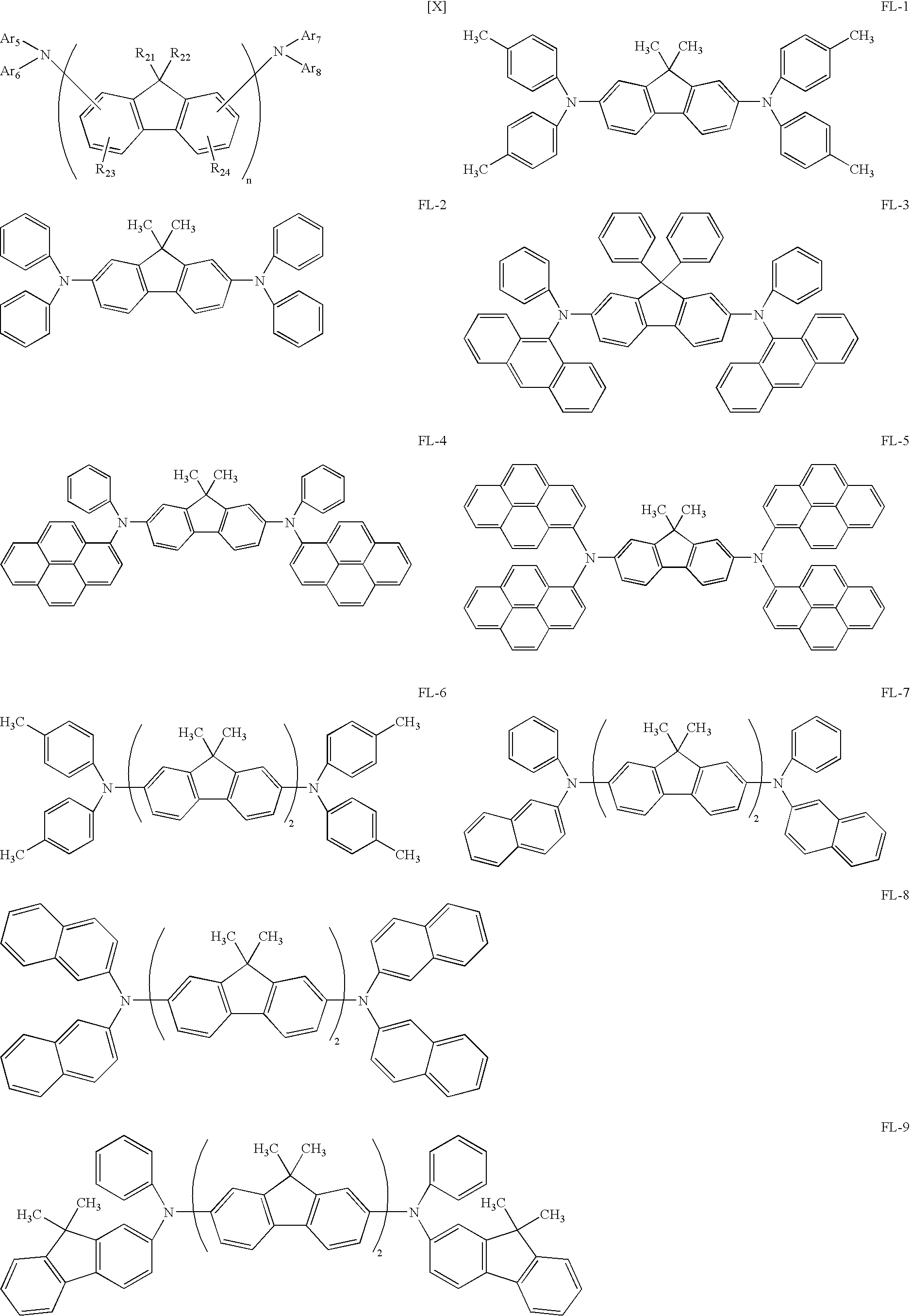


Preferable examples of the organic luminescence device are shown in FIGS. 1 to 6 , respectively.
However, in FIGS. 1 to 6 , there are shown common basic device configurations. The configuration of the organic luminescence device using the compound of the present invention is not limited thereto. For instance, it is possible to adopt various layer configurations such as one in which an insulating layer is formed at the interface between the electrode and the organic layer, one in which an adhesive layer or an interference layer is formed, and one in which the hole-transporting layer is composed of two layers with different ionization potentials.
The spiro compounds represented by the general formula [I] or the general formula [II] to be used in the present invention are compounds each having excellent electron-transporting property, luminescence property, and durability as compared with the conventional compounds, and-they can be used in any modes of FIGS. 1 to 6 .
In the present invention, the spiro compounds represented by the general formula [I] or the general formula [II] are used as structural components of the electron-transporting layer or the luminescent layer. However, hole-transporting compounds, luminescent compounds, electron-transporting compounds, or the like, which have been known, may be used together if required.
The examples of those compounds will be given below.
Hole-transporting Compound


Electron-transporting Luminescent Material


Luminescent Material

Luminescent Layer Matrix Material and Electron-transporting Material

Polymeric Hole-transporting Material


Polymeric Luminescent Material and Charge-transporting Material

In the organic luminescence device of the present invention, the layer containing the spiro compound represented by the general formula [I] or the general formula [II] and the layer containing another organic compound are generally formed as thin films by a vacuum evaporation method, or by a coating method after being dissolved in an appropriate solvent. In particular, in the case of forming a film with a coating method, the film may be formed in combination with an appropriate binder resin.
The above binder resin can be selected from a wide variety of the binder resins including, for example, polyvinyl carbazole resin, polycarbonate resin, polyester resin, polyarylate resin, polystyrene resin, acrylic resin, methacryl resin, butyral resin, polyvinyl acetal resin, diallyl phthalate resin, phenol resin, epoxy resin, silicone resin, polysulfone resin, and urea resin, although not limited to them. In addition, those resins may be used solely or one or more resins may be combined with each other as a copolymer.
The anode material may be one preferably having a large work function. For example, a simple metal substance such as gold, platinum, nickel, palladium, cobalt, selenium, or vanadium, or an alloy thereof, or a metal oxide such as tin oxide, zinc oxide, indium tin oxide (ITO), or indium zinc oxide can be used. In addition, a conductive polymer such as polyaniline, polypyrrole, polythiophene, or polyphenylene sulfide can be also used. Those electrode substances may be used solely or two or more substances may be used together.
On the other hand, the cathode material may be one preferably having a small work function. For example, a simple metal substance such as lithium, sodium, potassium, cesium, calcium, magnesium, aluminum, indium, silver, lead, tin, or chromium, or an alloy of plural substances can be used. It is also possible to use a metal oxide such as indium tin oxide (ITO). In addition, the cathode may be constructed as a single layer or may have a multi-layer configuration.
The substance used in the present invention may be, although not particularly limited to, a non-transparent substrate such as a metallic substrate or a ceramic substrate, or a transparent substrate formed of glass, quartz, plastic sheets, or the like. In addition, it is also possible to control the luminescence color light by using a color filter film, a fluorescent color-converting filter film, or a dielectric reflection film as a substrate.
Furthermore, a protective layer or a sealing layer may be formed on the prepared device for preventing the device from contacting with oxygen, moisture, or the like. The protective layer may be a diamond thin film, a film made of an inorganic material such as a metal oxide or a metal nitride, or a polymer film made of a fluorocarbon resin, polyparaxylene, polyethylene, a silicone resin, or a polystyrene resin, or furthermore it may be a photo-curing resin. Furthermore, it is also possible to package the device itself with an appropriate sealing resin while covering it with a glass, a gas-impermeable film, a metal, or the like.
Hereinafter, the present invention will be described more specifically with examples. However, the present invention is not limited to those examples.
[Synthesis of Exemplified Compound No. 1]

In a 500-ml three-neck flask, 2.0 g (3.16 mmol) of 2,2′-7,7′-tetrabromo-9,9′-spirobifluorene [1]*1), 4.5 g (19.0 mmol) of 9,9-dimethylfluorene-2-boronic acid [2], 140 ml of toluene, and 70 ml of ethanol were added, and an aqueous solution of 25 g of sodium carbonate/130 ml of water was dropped thereto with stirring in a nitrogen atmosphere at room temperature, followed by the addition of 0.7 g (0.63 mmol) of tetrakis (triphenylphosphine) palladium (0). After stirring the mixture for 30 minutes at room temperature, the temperature is allowed to rise to 77° C., followed by stirring for 8 hours. After the reaction, an organic layer was extracted with chloroform and was then dried with anhydrous sodium sulfate, followed by purification with a silica gel column (hexane+toluene mixture developing solvent). Consequently, 2.5 g (73% yield) of the exemplified compound No. 1 (white crystal) was obtained.
[Synthesis of Exemplified Compound No. 7]

In a 500-ml three-neck flask, 2.0 g (3.16 mmol) of 2,2′-7,7′-tetrabromo-9,9′-spirobifluorene [1], 4.7 g (19.0 mmol) of pyrene-1-boronic acid [2], 140 ml of toluene, and 70 ml of ethanol were added, and an aqueous solution of 25 g of sodium carbonate/130 ml of water was dropped with stirring in a nitrogen atmosphere at room temperature, followed by the addition of 0.7 g (0.63 mmol) of tetrakis (triphenylphosphine) palladium (0). After stirring the mixture for 30 minutes at room temperature, the temperature is allowed to rise to 77° C., followed by stirring for 8 hours. After the reaction, an organic layer was extracted with chloroform and was then dried with anhydrous sodium sulfate, followed by purification with a silica gel column (hexane+toluene mixture developing solvent). Consequently, 2.3 g (65% yield) of the exemplified compound No. 7 (white crystal) was obtained.
[Synthesis of Exemplified Compound No. 14]

In a 300-ml three-neck flask, 2.0 g (3.16 mmol) of 2,2′-7,7′-tetrabromo-9,9′-spirobifluorene [1], 3.2 g (19.0 mmol) of carbazole [2], and 150 ml of xylene were added, and 2.0 g (20.9 mmol) of t-butoxy sodium was added thereto with stirring in a nitrogen atmosphere at room temperature, followed by heating the mixture to a temperature of 50° C. In this mixture, a 5-ml xylene solution of 0.035 g (0.16 mmol) of palladium acetate and 0.032 g (0.16 mmol) of tri-t-butylphosphine was added, followed by heating the mixture to 130° C. and stirring for 8 hours. After the reaction, an organic layer was extracted with chloroform and was then dried with anhydrous sodium sulfate, followed by purification with a silica gel column (hexane+toluene mixture developing solvent). Consequently, 1.7 g (55% yield) of the exemplified compound No. 14 (white crystal) was obtained.
[Synthesis of Exemplified Compound No. 20]

In a 300-ml three-neck flask, 3.0 g (9.02 mmol) of 5,5′-spirobi(dibenzosilole) [1]*2) and 100 ml of chloroform were added, and then 0.07 g (0.45 mmol) of iron chloride (III) was added with stirring at 0° C., followed by dropping 5.9 g (37.0 mmol) of bromine. After stirring the mixture for 6 hours at room temperature, an organic layer was extracted with chloroform and was then washed with a sodium thiosulfate aqueous solution, followed by drying with anhydrous sodium sulfate. A crystal obtained by distilling off the solvent was re-crystallized with chloroform, resulting in 4.0 g (69% yield) of tetrabromo-5,5′-spiro(dibenzosilole) [2] (white crystal).
Next, in a 500-ml three-neck flask, 2.0 g (3.09 mmol) of [2], 4.4 g (18.5 mmol) of 9,9-dimethylfluorene-2-boronic acid [3], 140 ml of toluene, and 70 ml of ethanol were added, and an aqueous solution of 25 g of sodium carbonate/130 ml of water was dropped in a nitrogen atmosphere, followed by the addition of 0.5 g (0.43 mmol) of tetrakis (triphenylphosphine) palladium (0). After stirring the mixture for 30 minutes at room temperature, the temperature is allowed to rise to 77° C., followed by stirring for 8 hours. After the reaction, an organic layer was extracted with chloroform and was then dried with anhydrous sodium sulfate, followed by purification with a silica gel column (hexane+toluene mixture developing solvent). Consequently, 2.2 g (64% yield) of the exemplified compound No. 20 (white crystal) was obtained.
A device having the structure shown in FIG. 2 was prepared.
On a glass substrate as a substrate 1, indium tin oxide (ITO) is deposited into a film with a thickness of 120 nm by a sputtering method to obtain an anode 2, so that the substrate thus formed is used as a transparent conductive support substrate. This was sequentially subjected to ultrasonic cleanings with acetone and isopropyl alcohol (IPA), and was then washed with IPA by boiling, followed by drying. Furthermore, one subjected to UV/ozone cleaning was used as a transparent conductive support substrate.
On the transparent conductive support substrate, a chloroform solution of the compound represented by the following structural formula was coated into a film of 30 nm in thickness by a spin-coating method, resulting in a hole-transporting layer 5.

Furthermore, an electron-transporting layer 6 was formed by forming a film of 50 nm in thickness from a spiro compound represented by the exemplified compound No. 1 by a vacuum evaporation method. The film formation was performed under the conditions in which the degree of vacuum at the time of evaporation was 1.0×10⁻⁴Pa and the film formation rate was 0.2 to 0.3 nm/sec.
A metal layer film of 50 nm in thickness was formed on the above organic layer as a cathode 4 by using an evaporation material including aluminum and lithium (lithium concentration: 1% by atom) by a vacuum evaporation method, and further an aluminum layer of 150 nm in thickness was formed by a vacuum evaporation method. The film formation was performed under the conditions in which the degree of vacuum at the time of evaporation was 1.0×10⁻⁴Pa and the film formation rate was 1.0 to 1.2 nm/sec.
Furthermore, the resulting product was covered with a protective glass plate in a nitrogen atmosphere and was then sealed with an acrylic resin adhesive.
When a direct current voltage of 10 V was applied on the device obtained in this way with an ITO electrode (anode 2) provided as a positive electrode and an Al—Li electrode (cathode 4) provided as a negative electrode, the current was caused to flow into the device at a current density of 11.5 mA/cm2 and blue-colored luminescence at a luminance of 3800 cd/m2 was observed.
Furthermore, when the current density was kept at 10.0 mA/cm2 and the voltage was applied for 100 hours, an initial luminance of 3500 cd/m2 changed to a luminance of 3300 cd/m2 after 100 hours, indicating small deterioration of luminance.
Devices were prepared and evaluated in the same way as that of Example 1, except that the exemplified compounds shown in Table 1 were used in place of the exemplified compound No. 1. The results are shown in Table 1.
Devices were prepared and evaluated in the same way as that of Example 1, except that the compounds represented by the following structural formula were used in place of the exemplified compound No. 1. The results are shown in Table 1.
Comparative Compound No. 1

Comparative Compound No. 2

Comparative Compound No. 3

| TABLE 1 | |||
| Initial stage | Durability | ||
| Exemplified | Applied | Current | Initial | Luminance after | ||
| compound | voltage | Luminance | density | luminance | 100-hour | |
| Example No. | No. | (V) | (cd/m2) | (mA/cm2) | (cd/m2) | (cd/m2) |
| Example 1 | 1 | 10 | 3800 | 10.0 | 3500 | 3300 | |
| 2 | 5 | 10 | 4500 | 10.0 | 4100 | 3800 | |
| 3 | 7 | 10 | 3500 | 10.0 | 3300 | 3200 | |
| 4 | 10 | 10 | 2900 | 10.0 | 2700 | 2500 | |
| 5 | 13 | 10 | 3800 | 10.0 | 3500 | 3400 | |
| 6 | 16 | 10 | 2400 | 10.0 | 2200 | 1900 | |
| 7 | 18 | 10 | 2400 | 10.0 | 2300 | 2200 | |
| 8 | 21 | 10 | 3600 | 10.0 | 3500 | 3300 | |
| 9 | 24 | 10 | 2700 | 10.0 | 2600 | 2200 | |
| 10 | 27 | 10 | 2300 | 10.0 | 2100 | 2000 | |
| | Comparative | 1 | 10 | 850 | 10.0 | 800 | 550 |
| Example 1 | |||||||
| 2 | |
10 | 700 | 10.0 | 650 | 250 | |
| 3 | |
10 | 400 | 10.0 | 350 | 100 | |
A device having the structure shown in FIG. 3 was prepared.
In the same manner as in Example 1, a hole-transporting layer 5 was formed on the transparent conductive support substrate.
Further, a luminescent layer 3 was formed by forming a film of 20 nm in thickness from a spiro compound represented by the exemplified compound No. 3 by a vacuum evaporation method. The film formation was performed under the conditions in which the degree of vacuum at the time of evaporation was 1.0×10⁻⁴Pa and the film formation rate was 0.2 to 0.3 nm/sec.
Furthermore, an electron-transporting layer 6 was formed by forming a film of 40 nm in thickness from aluminum tris quinolinol by a vacuum evaporation method. The film formation was performed under the conditions in which the degree of vacuum at the time of evaporation was 1.0×10⁻⁴Pa and the film formation rate was 0.2 to 0.3 nm/sec.
Next, after forming a cathode 4 in the same manner as in Example 1, the resulting product was sealed.
When a direct current voltage of 8 V was applied on the device obtained in this way with an ITO electrode (anode 2) provided as a positive electrode and an Al—Li electrode (cathode 4) provided as a negative electrode, the current was caused to flow into the device at a current density of 12.0 MA/cm2 and blue-colored luminescence at a luminance of 6700 cd/m2 was observed.
Furthermore, when the current density was kept at 10.0 mA/cm2 and the voltage was applied for 100 hours, an initial luminance of 5500 cd/m2 changed to a luminance of 5200 cd/m2 after 100 hours, indicating small deterioration of luminance.
Devices were prepared and evaluated in the same way as that of Example 11, except that the exemplified compounds shown in Table 2 were used in place of the exemplified compound No. 3. The results are shown in Table 2.
Devices were prepared and evaluated in the same way as that of Example 11, except that the comparative compounds No. 1 to No. 3 were used in place of the exemplified compound No. 3. The results are shown in Table 2.
| TABLE 2 | |||
| Initial stage | Durability | ||
| Exemplified | Applied | Current | Initial | Luminance after | ||
| compound | voltage | Luminance | density | luminance | 100-hour | |
| Example No. | No. | (V) | (cd/m2) | (mA/cm2) | (cd/m2) | (cd/m2) |
| Example 11 | 3 | 8 | 6700 | 10.0 | 5500 | 5200 | |
| 12 | 6 | 8 | 6500 | 10.0 | 5200 | 4800 | |
| 13 | 8 | 8 | 7300 | 10.0 | 6000 | 5700 | |
| 14 | 11 | 8 | 5200 | 10.0 | 4400 | 4100 | |
| 15 | 15 | 8 | 3900 | 10.0 | 3600 | 3400 | |
| 16 | 19 | 8 | 5100 | 10.0 | 4200 | 4000 | |
| 17 | 23 | 8 | 5600 | 10.0 | 4600 | 4300 | |
| 18 | 25 | 8 | 3600 | 10.0 | 2700 | 2500 | |
| 19 | 26 | 8 | 3800 | 10.0 | 2900 | 2600 | |
| 20 | 28 | 8 | 5200 | 10.0 | 4100 | 3800 | |
| | Comparative | 1 | 8 | 800 | 10.0 | 770 | 450 |
| Example 4 | |||||||
| 5 | |
8 | 500 | 10.0 | 400 | 150 | |
| 6 | |
8 | 1200 | 10.0 | 900 | 300 | |
A device having the structure shown in FIG. 3 was prepared.
On a transparent conductive support substrate similar to that in Example 1, a chloroform solution of a compound represented by the following structural formula was applied into a film of 20 nm in thickness by a spin-coating method, resulting in a hole-transporting layer 5.

Furthermore, the spiro compound represented as the exemplified compound No. 7 and the fluorene compound represented as the exemplified compound No. FL-1 (weight ratio of 100:1) were deposited into a film with a thickness of 20 nm by the vacuum evaporation method to form a luminescent layer 3. The film formation was performed under the conditions in which the degree of vacuum at the time of evaporation was 1.0×10⁻⁴Pa and the film formation rate was 0.2 to 0.3 nm/sec.
Furthermore, an electron-transporting layer 6 was formed by forming a film of 40 nm in thickness from aluminum tris quinolinol by a vacuum evaporation method. The film formation was performed under the conditions in which the degree of vacuum at the time of evaporation was 1.0×10⁻⁴Pa and the film formation rate was 0.2 to 0.3 nm/sec.
Next, after forming a cathode 4 in the same manner as in Example 1, the resulting product was sealed.
When a direct current voltage of 8 V was applied on the device obtained in this way with an ITO electrode (anode 2) provided as a positive electrode and an Al—Li electrode (cathode 4) provided as a negative electrode, the current was caused to flow into the device at a current density of 13.5 mA/cm2 and blue-colored luminescence at a luminance of 16000 cd/m2 was observed.
Furthermore, when the current density was kept at 10.0 mA/cm2 and the voltage was applied for 100 hours, the initial luminance of 12000 cd/m2 changed to a luminance of 9000 cd/m2 after 100 hours, indicating small deterioration of luminance.
Devices were prepared and evaluated in the same way as that of Example 21, except that the exemplified fluorene compound shown in Table 3 was used in place of the exemplified fluorene compound No. FL-1. The results are shown in Table 3.
Devices were prepared and evaluated in the same way as that of Example 21, except that the comparative compounds No. 1 to No. 3 were used in place of the exemplified compound No. 7. The results are shown in Table 3.
| TABLE 3 | |||
| Initial stage | Durability | ||
| Exemplified | Exemplified | Applied | Current | Initial | Luminance after | ||
| compound | fluorene | voltage | Luminance | density | luminance | 100-hour | |
| Example No. | No. | compound No. | (V) | (cd/m2) | (mA/cm2) | (cd/m2) | (cd/m2) |
| Example 21 | 7 | FL-1 | 8 | 16000 | 10.0 | 12000 | 9000 |
| 22 | 7 | FL-2 | 8 | 15000 | 10.0 | 12000 | 8000 |
| 23 | 7 | FL-3 | 8 | 17000 | 10.0 | 14000 | 10000 |
| 24 | 7 | FL-4 | 8 | 12000 | 10.0 | 8500 | 7000 |
| 25 | 7 | FL-5 | 8 | 9000 | 10.0 | 7000 | 6000 |
| 26 | 7 | FL-6 | 8 | 19000 | 10.0 | 14000 | 11000 |
| 27 | 7 | FL-7 | 8 | 20000 | 10.0 | 14000 | 12000 |
| 28 | 7 | FL-9 | 8 | 22000 | 10.0 | 17000 | 13000 |
| 29 | 7 | FL-10 | 8 | 21000 | 10.0 | 16000 | 13000 |
| 30 | 7 | FL-12 | 8 | 17000 | 10.0 | 11000 | 8500 |
| 31 | 7 | FL-13 | 8 | 13000 | 10.0 | 10000 | 7000 |
| 32 | 7 | FL-14 | 8 | 18000 | 10.0 | 16000 | 14000 |
| 33 | 7 | FL-15 | 8 | 19000 | 10.0 | 16000 | 14000 |
| 34 | 7 | FL-18 | 8 | 19000 | 10.0 | 17000 | 15000 |
| 35 | 7 | FL-21 | 8 | 23000 | 10.0 | 19000 | 16000 |
| 36 | 7 | FL-24 | 8 | 24000 | 10.0 | 19000 | 17000 |
| 37 | 7 | FL-26 | 8 | 9500 | 10.0 | 8000 | 6000 |
| 38 | 7 | FL-27 | 8 | 17000 | 10.0 | 13000 | 11000 |
| 39 | 7 | FL-28 | 8 | 10000 | 10.0 | 8000 | 6500 |
| 40 | 7 | FL-29 | 8 | 8000 | 10.0 | 7000 | 6000 |
| 41 | 7 | FL-30 | 8 | 9500 | 10.0 | 8000 | 6500 |
| 42 | 7 | FL-31 | 8 | 12000 | 10.0 | 10000 | 7000 |
| 43 | 7 | FL-32 | 8 | 23000 | 10.0 | 18000 | 15000 |
| 44 | 7 | FL-33 | 8 | 23000 | 10.0 | 17000 | 14000 |
| 45 | 7 | FL-36 | 8 | 25000 | 10.0 | 19000 | 16000 |
| 46 | 7 | FL-37 | 8 | 25000 | 10.0 | 18000 | 15000 |
| 47 | 7 | FL-38 | 8 | 20000 | 10.0 | 17000 | 14000 |
| 48 | 7 | FL-39 | 8 | 24000 | 10.0 | 19000 | 16000 |
| 49 | 7 | FL-41 | 8 | 26000 | 10.0 | 20000 | 16000 |
| 50 | 7 | FL-42 | 8 | 26000 | 10.0 | 21000 | 17000 |
| 51 | 7 | FL-44 | 8 | 15000 | 10.0 | 12000 | 9500 |
| 52 | 7 | FL-45 | 8 | 12000 | 10.0 | 9000 | 7500 |
| 53 | 7 | FL-46 | 8 | 13000 | 10.0 | 11000 | 7000 |
| Comparative | Comparative | FL-1 | 8 | 3000 | 10.0 | 2500 | 900 |
| Example 7 | 1 | ||||||
| 8 | Comparative | FL-1 | 8 | 2000 | 10.0 | 1500 | 200 |
| 2 | |||||||
| 9 | Comparative | FL-1 | 8 | 4500 | 10.0 | 3500 | 600 |
| 3 | |||||||
A device having the structure shown in FIG. 3 was prepared.
On a transparent conductive support substrate similar to that in Example 1, a chloroform solution of a compound represented by the following structural formula was applied into a film of 20 nm in thickness by a spin-coating method, resulting in a hole-transporting layer 5.

Furthermore, the spiro compound represented as the exemplified compound No. 2 and a compound represented by the following structural formula (weight ratio of 100:5) were deposited into a film with a thickness of 20 nm by the vacuum evaporation method to form a luminescent layer 3. The film formation was performed under the conditions in which the degree of vacuum at the time of evaporation was 1.0×10⁻⁴Pa and the film formation rate was 0.2 to 0.3 nm/sec.

Furthermore, an electron-transporting layer 6 was formed by forming a film of 40 nm in thickness from bathophenanthroline (BPhen) by the vacuum evaporation method. The film formation was performed under the conditions in which the degree of vacuum at the time of evaporation was 1.0×10⁻⁴Pa and the film formation rate was 0.2 to 0.3 nm/sec.
Next, after forming a cathode 4 in the same manner as in Example 1, the resulting product was sealed.
When a direct current voltage of 8 V was applied on the device obtained in this way with an ITO electrode (anode 2) provided as a positive electrode and an Al—Li electrode (cathode 4) provided as a negative electrode, the current was caused to flow into the device at a current density of 10.5 mA/cm2 and green-colored luminescence at a luminance of 9000 cd/m2 was observed.
Furthermore, when the current density was kept at 7.0 mA/cm2 and the voltage was applied for 100 hours, the initial luminance of 7500 cd/m2 changed to a luminance of 6500 cd/m2 after 100 hours, indicating small deterioration of luminance.
Devices were prepared and evaluated in the same way as that of Example 54, except that the exemplified compound shown in Table 4 was used in place of the exemplified compound No. 2. The results are shown in Table 4.
Devices were prepared and evaluated in the same way as that of Example 54, except that the comparative compounds No. 1 to No. 3 were used in place of the exemplified compound No. 2. The results are shown in Table 4.
| TABLE 4 | |||
| Initial stage | Durability | ||
| Exemplified | Applied | Initial | Luminance | |||
| compound | voltage | Luminance | Current density | luminance | after 100-hour | |
| Example No. | No. | (V) | (cd/m2) | (mA/cm2) | (cd/m2) | (cd/m2) |
| Example 54 | 2 | 8 | 9000 | 7.0 | 7500 | 6500 | |
| 55 | 4 | 8 | 9500 | 7.0 | 8000 | 6500 | |
| 56 | 6 | 8 | 7000 | 7.0 | 6000 | 5000 | |
| 57 | 12 | 8 | 8000 | 7.0 | 6000 | 5500 | |
| 58 | 14 | 8 | 14000 | 7.0 | 11000 | 9000 | |
| 59 | 15 | 8 | 10000 | 7.0 | 9000 | 7500 | |
| 60 | 20 | 8 | 10000 | 7.0 | 8000 | 7000 | |
| 61 | 22 | 8 | 9500 | 7.0 | 8000 | 7500 | |
| 62 | 29 | 8 | 15000 | 7.0 | 13000 | 10000 | |
| 63 | 30 | 8 | 8500 | 7.0 | 8000 | 7000 | |
| | Comparative | 1 | 8 | 1300 | 7.0 | 900 | 300 |
| Example 10 | |||||||
| 11 | |
8 | 1000 | 7.0 | 900 | 100 | |
| 12 | |
8 | 2500 | 7.0 | 2000 | 700 | |
A device having the structure shown in FIG. 1 was prepared.
On a transparent conductive support substrate which was similar to that of Example 1, a solution prepared by dissolving 0.050 g of a spiro compound represented by the exemplified compound No. 1 and 1.00 g of poly-N-vinyl carbazole (a weight average molecular weight=63,000) in 80 ml of chloroform was applied into a film of 120 nm in thickness by a spin-coating method (rotation speed=2000 rpm) to form an organic layer (a luminescent layer 3).
Next, after forming a cathode 4 in the same manner as in Example 1, the resulting product was sealed.
When a direct current voltage of 10 V was applied on the device obtained in this way with an ITO electrode (anode 2) provided as a positive electrode and an Al—Li electrode (cathode 4) provided as a negative electrode, the current was caused to flow into the device at a current density of 8.0 mA/cm2 and blue-colored luminescence at a luminance of 1900 cd/m2 was observed.
Furthermore, when the current density was kept at 5.0 mA/cm2 and the voltage was applied for 100 hours in the nitrogen atmosphere, the initial luminance of 1000 cd/m2 changed to a luminance of 850 cd/m2 after 100 hours, indicating small deterioration of luminance.
Devices were prepared and evaluated in the same way as that of Example 64, except that the exemplified compound shown in Table 5 was used in place of the exemplified compound No. 1. The results are shown in Table 5.
Devices were prepared and evaluated in the same way as that of Example 64, except that the comparative compounds No. 1 to No. 3 were used in place of the exemplified compound No. 1. The results are shown in Table 5.
| TABLE 5 | |||
| Initial stage | Durability | ||
| Exemplified | Applied | Current | Initial | Luminance after 100- | ||
| compound | voltage | Luminance | density | luminance | hour | |
| Example No. | No. | (V) | (cd/m2) | (mA/cm2) | (cd/m2) | (cd/m2) |
| Example 64 | 1 | 10 | 1900 | 5.0 | 1000 | 850 | |
| 65 | 7 | 10 | 2500 | 5.0 | 1600 | 1400 | |
| 66 | 19 | 10 | 1400 | 5.0 | 1000 | 800 | |
| 67 | 20 | 10 | 1800 | 5.0 | 1400 | 1300 | |
| 68 | 24 | 10 | 1900 | 5.0 | 1200 | 950 | |
| | Comparative | 1 | 10 | 300 | 5.0 | 200 | No luminescence |
| Example 13 | |||||||
| 14 | |
10 | 200 | 5.0 | 150 | No luminescence | |
| 15 | |
10 | 550 | 5.0 | 400 | 50 | |
As described with reference to the embodiments and the examples, the organic luminescence device using the spiro compound represented by the general formula [I] or the general formula [II] provides luminescence with a high luminance by the application of a low voltage and is excellent in durability.
In particular, the organic layer containing the spiro compound of the present invention is excellent as an electron-transporting layer and is also excellent as a luminescent layer.
Furthermore, the device can be prepared by using a vacuum evaporation method or a casting method, so that the device having a large area can be easily prepared at a comparatively low cost.
Claims (2)
1. An organic luminescence device comprising at least a pair of electrodes including an anode and a cathode and one or a plurality of layers containing an organic compound sandwiched between the pair of electrodes, wherein at least one of the layers containing the organic compound contains at least one spiro compound represented by the following general formula [II]:

wherein R5, R6, R7, and R8 represent a hydrogen atom, a substituted or unsubstituted alkyl group, a substituted or unsubstituted aralkyl group, a substituted or unsubstituted aryl group, a substituted or unsubstituted heterocyclic group, a substituted amino group, cyano group, or a halogen atom, and R5, R6, R7, and R8, may be identical or different from each other; and Ar3 and Ar4 represent a substituted or unsubstituted condensed polycyclic aromatic group or a substituted or unsubstituted condensed polycyclic heterocyclic group, which may be identical or different from each other and wherein at least one of Ar3 and Ar4 is a condensed polycyclic aromatic group represented by one of the following general formula [III] to [VIII]:

wherein R9 represents a hydrogen atom, a substituted or unsubstituted alkyl group, a substituted or unsubstituted aralkyl group, a substituted or unsubstituted aryl group, a substituted or unsubstituted heterocyclic group, a substituted amino group, a cyano group, or a halogen atom; and R10 and R11 represent a hydrogen atom, a substituted or unsubstituted alkyl group, a substituted or unsubstituted aralkyl group, a substituted or unsubstituted aryl group, or a substituted or unsubstituted heterocyclic group, which may be identical or different from each other;

wherein R12 represents a hydrogen atom, a substituted or unsubstituted alkyl group, a substituted or unsubstituted aralkyl group, a substituted or unsubstituted aryl group, a substituted or unsubstituted heterocyclic group, a substituted amino group, a cyano group, or a halogen atom; and R13 and R14 represent a hydrogen atom, a substituted or unsubstituted alkyl group, a substituted or unsubstituted aralkyl group, a substituted or unsubstituted aryl group, or a substituted or unsubstituted heterocyclic group, which may be identical or different from each other; and

wherein R15 to R18 represent a hydrogen atom, a substituted or unsubstituted alkyl group, a substituted or unsubstituted aralkyl group, a substituted or unsubstituted aryl group, a substituted or unsubstituted heterocyclic group, a substituted amino group, a cyano group, or a halogen atom; and
wherein at least a luminescent layer among the layers containing the organic compound contains at least one of the spiro compounds and a fluorene compound represented by the following general formula [X]:

wherein R21 and R22 represent a hydrogen atom, a substituted or unsubstituted alkyl group, a substituted or unsubstituted aralkyl group, a substituted or unsubstituted aryl group, or a substituted or unsubstituted heterocyclic group, R21 themselves or R22 themselves, which are bonded to different fluorene groups, may be identical or different from each other, and R21 and R22 that are bonded to the same fluorene group may be identical or different from each other; R23 and R24 represent a hydrogen atom, a substituted or unsubstituted alkyl group, a substituted or unsubstituted aralkyl group, a substituted or unsubstituted aryl group, a substituted or unsubstituted heterocyclic group, a cyano group, or a halogen atom, and R23 themselves or R24 themselves, which are bonded to different fluorene groups, may be identical or different from each other, and R23 and R24 that are bonded to the same fluorene group may be identical or different from each other; Ar5, Ar6, Ar7, and Ar8 represent a substituted or unsubstituted aromatic group, a substituted or unsubstituted heterocyclic group, a substituted or unsubstituted condensed polycyclic aromatic group, or a substituted or unsubstituted condensed polycyclic heterocyclic group, which may be identical or different from each other, and Ar5 and Ar6 as well as Ar7 and Ar8 may be bonded with each other to form rings, respectively; and n represents an integral number of 1 to 10.
2. An organic luminescence device comprising at least a pair of electrodes including an anode and a cathode and one or a plurality of layers containing an organic compound sandwiched between the pair of electrodes, wherein at least one of the layers containing the organic compound contains at least one spiro compound represented by the following general formula [II]:

wherein R5, R6, R7, and R8 represent a hydrogen atom, a substituted or unsubstituted alkyl group, a substituted or unsubstituted aralkyl group, a substituted or unsubstituted aryl group, a substituted or unsubstituted heterocyclic group, a substituted amino group, cyano group, or a halogen atom, and R5, R6, R7, and R8 may be identical or different from each other; and Ar3 and Ar4 represent a substituted or unsubstituted condensed polycyclic aromatic group or a substituted or unsubstituted condensed polycyclic heterocyclic group, which may be identical or different from each other and wherein at least one of Ar3 and Ar4 is a condensed polycyclic aromatic group represented by one of the following general formula [III] to [VIII]:

wherein R9 represents a hydrogen atom, a substituted or unsubstituted alkyl group, a substituted or unsubstituted aralkyl group, a substituted or unsubstituted aryl group, a substituted or unsubstituted heterocyclic group, a substituted amino group, a cyano group, or a halogen atom; and R10 and R11 represent a hydrogen atom, a substituted or unsubstituted alkyl group, a substituted or unsubstituted aralkyl group, a substituted or unsubstituted aryl group, or a substituted or unsubstituted heterocyclic group, which may be identical or different from each other;

wherein R12 represents a hydrogen atom, a substituted or unsubstituted alkyl group, a substituted or unsubstituted aralkyl group, a substituted or unsubstituted aryl group, a substituted or unsubstituted heterocyclic group, a substituted amino group, a cyano group, or a halogen atom; and R13 and R14 represent a hydrogen atom, a substituted or unsubstituted alkyl group, a substituted or unsubstituted aralkyl group, a substituted or unsubstituted aryl group, or a substituted or unsubstituted heterocyclic group, which may be identical or different from each other; and

wherein R15 to R18 represent a hydrogen atom, a substituted or unsubstituted alkyl group, a substituted or unsubstituted aralkyl group, a substituted or unsubstituted aryl group, a substituted or unsubstituted heterocyclic group, a substituted amino group, a cyano group, or a halogen atom; and
wherein at least a luminescent layer among the layers containing the organic compound contains at least one of the spiro compounds and a fluorene compound represented by the following general formula [XI]:

(wherein R25 and R26 represent a hydrogen atom, a substituted or unsubstituted alkyl group, a substituted or unsubstituted aralkyl group, a substituted or unsubstituted aryl group, or a substituted or unsubstituted heterocyclic group, R25 themselves or R26 themselves, which are bonded to different fluorene groups, may be identical or different from each other, and R25 and R26 that are bonded to the same fluorene group may be identical or different from each other; R27 and R28 represent a hydrogen atom, a substituted or unsubstituted alkyl group, a substituted or unsubstituted aralkyl group, a substituted or unsubstituted aryl group, a substituted or unsubstituted heterocyclic group, a cyano group, or a halogen atom, and R27 themselves or R28 themselves, which are bonded to different fluorene groups, may be identical or different from each other, and R27 and R28 that are bonded to the same fluorene group may be identical or different from each other; Ar9 and Ar10 represent a substituted or unsubstituted divalent aromatic group or a substituted or unsubstituted divalent heterocyclic group, which may be identical or different from each other; Ar11, Ar12, Ar13, and Ar14 represent a substituted or unsubstituted aromatic group, a substituted or unsubstituted heterocyclic group, a substituted or unsubstituted condensed polycyclic aromatic group, or a substituted or unsubstituted condensed polycyclic heterocyclic group, which may be identical or different from each other, and Ar11 and Ar12 as well as Ar13 and Ar14 may be bonded with each other to form rings, respecdvely; and m represents an integral number of 1 to 10.)
Applications Claiming Priority (3)
| Application Number | Priority Date | Filing Date | Title |
|---|---|---|---|
| JP2002246601A JP3848224B2 (en) | 2002-08-27 | 2002-08-27 | Spiro compound and organic light emitting device using the same |
| JP2002-246601 | 2002-08-27 | ||
| PCT/JP2003/010258 WO2004020373A1 (en) | 2002-08-27 | 2003-08-12 | Spiro compound and organic luminescence device using the same |
Publications (2)
| Publication Number | Publication Date |
|---|---|
| US20060134425A1 US20060134425A1 (en) | 2006-06-22 |
| US7510781B2 true US7510781B2 (en) | 2009-03-31 |
Family
ID=31972426
Family Applications (1)
| Application Number | Title | Priority Date | Filing Date |
|---|---|---|---|
| US10/525,327 Expired - Fee Related US7510781B2 (en) | 2002-08-27 | 2003-08-12 | Spiro compound and organic luminescence device using the same |
Country Status (4)
| Country | Link |
|---|---|
| US (1) | US7510781B2 (en) |
| JP (1) | JP3848224B2 (en) |
| AU (1) | AU2003253441A1 (en) |
| WO (1) | WO2004020373A1 (en) |
Cited By (4)
| Publication number | Priority date | Publication date | Assignee | Title |
|---|---|---|---|---|
| US20070015005A1 (en) * | 2005-07-07 | 2007-01-18 | Chi Mei Optoelectronics Corp. | Organic electroluminescent device and host material of luminescent and hole-blocking material thereof |
| US20080166591A1 (en) * | 2006-12-27 | 2008-07-10 | Canon Kabushiki Kaisha | Carbazole compound and organic light-emitting device using same |
| CN102241700A (en) * | 2011-04-27 | 2011-11-16 | 华南师范大学 | 2,2',7,7'-spirosilabifluorene oligomer, and preparation method and application thereof |
| US9548457B2 (en) | 2005-09-30 | 2017-01-17 | Semiconductor Energy Laboratories Co., Ltd. | Spirofluorene derivative, material for light-emitting element, light-emitting element, light-emitting device, and electronic device |
Families Citing this family (42)
| Publication number | Priority date | Publication date | Assignee | Title |
|---|---|---|---|---|
| AU2003211786A1 (en) * | 2002-03-08 | 2003-09-22 | Canon Kabushiki Kaisha | Organic light-emitting device |
| JP4356363B2 (en) * | 2002-11-26 | 2009-11-04 | コニカミノルタホールディングス株式会社 | Organic electroluminescence element and display device having the same |
| US7862904B2 (en) * | 2003-07-21 | 2011-01-04 | Merck Patent Gmbh | Organic electroluminescent element |
| JP4581355B2 (en) * | 2003-09-09 | 2010-11-17 | 東洋インキ製造株式会社 | Organic electroluminescence device |
| JP4177737B2 (en) * | 2003-09-18 | 2008-11-05 | 三井化学株式会社 | Amine compound and organic electroluminescence device containing the amine compound |
| JP4576141B2 (en) * | 2004-03-26 | 2010-11-04 | 保土谷化学工業株式会社 | Carbazole derivatives containing fluorene groups |
| JP4576376B2 (en) * | 2004-03-26 | 2010-11-04 | 保土谷化学工業株式会社 | Carbazole derivatives containing fluorene groups and organic electroluminescent devices |
| US20080036365A1 (en) * | 2004-03-26 | 2008-02-14 | Hodogaya Chemical Co., Ltd. | Carbazole Derivative Containing Fluorene Group and Organic Electroluminescent Element |
| WO2005121064A1 (en) * | 2004-06-10 | 2005-12-22 | Semiconductor Energy Laboratory Co., Ltd. | Benzidine derivative, and light-emitting device and electric appliance using the benzidine derivative as the hole transporting material |
| JP4906037B2 (en) * | 2004-06-10 | 2012-03-28 | 株式会社半導体エネルギー研究所 | Benzidine derivative, hole transport material, light emitting device, and lighting device |
| WO2005123634A1 (en) | 2004-06-16 | 2005-12-29 | Idemitsu Kosan Co., Ltd. | Fluorene derivative and organic electroluminescent device using same |
| CN1976883A (en) * | 2004-06-28 | 2007-06-06 | 出光兴产株式会社 | Polycyclic aromatic compound, material for forming light-emitting coating film using the same, and organic electroluminescent device |
| JP2006140235A (en) * | 2004-11-10 | 2006-06-01 | Idemitsu Kosan Co Ltd | Organic electroluminescence element |
| JP4599142B2 (en) * | 2004-11-26 | 2010-12-15 | キヤノン株式会社 | Organic light emitting device |
| KR100708655B1 (en) | 2004-11-27 | 2007-04-18 | 삼성에스디아이 주식회사 | Organic electroluminescence display |
| US20080093986A1 (en) * | 2004-12-28 | 2008-04-24 | Idemitsu Kosan Co., Ltd. | Ink For Forming Organic El Coating Film And Method For Production Thereof |
| US20060186797A1 (en) * | 2005-02-15 | 2006-08-24 | Tosoh Corporation | Pi-conjugated compound having cardo structure, process for preparing same and use of same |
| JP4358884B2 (en) * | 2005-03-18 | 2009-11-04 | 出光興産株式会社 | Aromatic amine derivative and organic electroluminescence device using the same |
| JP4950460B2 (en) * | 2005-08-26 | 2012-06-13 | キヤノン株式会社 | Organic light emitting device |
| JP5103727B2 (en) * | 2005-11-16 | 2012-12-19 | 東ソー株式会社 | Fluorene compound and organic EL device using the same |
| JP5017884B2 (en) * | 2006-02-24 | 2012-09-05 | 東レ株式会社 | Light emitting device material and light emitting device |
| JP4823730B2 (en) * | 2006-03-20 | 2011-11-24 | 新日鐵化学株式会社 | Luminescent layer compound and organic electroluminescent device |
| JP5164389B2 (en) * | 2006-03-28 | 2013-03-21 | キヤノン株式会社 | Amino compound for organic light emitting device and organic light emitting device having the same |
| JP2008106032A (en) * | 2006-09-25 | 2008-05-08 | Kyushu Univ | Carbazole derivative and organic solid laser material using the same |
| JP5311785B2 (en) * | 2007-09-13 | 2013-10-09 | キヤノン株式会社 | Organic light emitting device and display device |
| JP5255296B2 (en) * | 2008-02-27 | 2013-08-07 | 東洋インキScホールディングス株式会社 | Materials and compounds for organic electroluminescence devices |
| KR101929837B1 (en) * | 2008-10-07 | 2018-12-18 | 유디씨 아일랜드 리미티드 | Siloles substituted with condensed ring systems and use thereof in organic electronics |
| DE102009032922A1 (en) * | 2009-07-14 | 2011-01-20 | Merck Patent Gmbh | Materials for organic electroluminescent devices |
| DE102009053645A1 (en) * | 2009-11-17 | 2011-05-19 | Merck Patent Gmbh | Materials for organic electroluminescent device |
| CN102167971B (en) * | 2011-03-02 | 2013-11-27 | 北京大学 | Blue-fluorescence luminescent material and application thereof |
| JP2012209452A (en) * | 2011-03-30 | 2012-10-25 | Sumitomo Chemical Co Ltd | Organic electroluminescent element |
| JP5828518B2 (en) * | 2011-07-15 | 2015-12-09 | 国立大学法人九州大学 | Delayed fluorescent material, organic electroluminescence device and compound using the same |
| WO2013123047A1 (en) * | 2012-02-14 | 2013-08-22 | Next Energy Technologies Inc. | Electronic devices using organic small molecule semiconducting compounds |
| WO2013123508A2 (en) | 2012-02-17 | 2013-08-22 | Next Energy Technologies, Inc. | Organic semiconducting compounds for use in organic electronic devices |
| KR102163770B1 (en) * | 2012-08-10 | 2020-10-12 | 메르크 파텐트 게엠베하 | Materials for organic electroluminescence devices |
| CN103409133B (en) * | 2013-07-18 | 2015-11-18 | 中节能万润股份有限公司 | A kind of electroluminescent material and application thereof |
| CN104804726A (en) * | 2015-03-19 | 2015-07-29 | 南京邮电大学 | Cross-shaped water-soluble conjugated blue-light-emitting material and preparation method thereof |
| US10770665B2 (en) | 2015-03-26 | 2020-09-08 | Next Energy Technology, Inc. | Fluorinated dye compounds for organic solar cells |
| KR102032599B1 (en) | 2015-10-06 | 2019-10-15 | 주식회사 엘지화학 | Amine compound and organic light emitting device comprising the same |
| CN107892695B (en) * | 2017-10-25 | 2020-04-21 | 南京邮电大学 | Organic polyspirolattice nano polymer material and preparation method thereof |
| CN108129441A (en) * | 2017-12-13 | 2018-06-08 | 南京邮电大学 | A kind of organic laser material of steric hindrance type multi-arm oligomerization fluorenes and preparation method thereof |
| CN112375002B (en) * | 2021-01-18 | 2021-05-07 | 苏州久显新材料有限公司 | 2,4, 7-trisubstituted fluorene compound and electronic device thereof |
Citations (32)
| Publication number | Priority date | Publication date | Assignee | Title |
|---|---|---|---|---|
| US4539507A (en) | 1983-03-25 | 1985-09-03 | Eastman Kodak Company | Organic electroluminescent devices having improved power conversion efficiencies |
| US4720432A (en) | 1987-02-11 | 1988-01-19 | Eastman Kodak Company | Electroluminescent device with organic luminescent medium |
| US4885211A (en) | 1987-02-11 | 1989-12-05 | Eastman Kodak Company | Electroluminescent device with improved cathode |
| JPH02247278A (en) | 1989-03-20 | 1990-10-03 | Idemitsu Kosan Co Ltd | Electroluminescence element |
| JPH03255190A (en) | 1990-01-22 | 1991-11-14 | Pioneer Electron Corp | Electroluminescent element |
| JPH04145192A (en) | 1990-10-04 | 1992-05-19 | Sumitomo Chem Co Ltd | Organic electroluminescence element |
| US5130603A (en) | 1989-03-20 | 1992-07-14 | Idemitsu Kosan Co., Ltd. | Organic electroluminescence device |
| US5151629A (en) | 1991-08-01 | 1992-09-29 | Eastman Kodak Company | Blue emitting internal junction organic electroluminescent device (I) |
| JPH05202356A (en) | 1991-09-11 | 1993-08-10 | Pioneer Electron Corp | Organic electroluminescence element |
| US5247190A (en) | 1989-04-20 | 1993-09-21 | Cambridge Research And Innovation Limited | Electroluminescent devices |
| JPH05247460A (en) | 1991-12-05 | 1993-09-24 | Sumitomo Chem Co Ltd | Organic electroluminescent device |
| US5317169A (en) | 1990-02-23 | 1994-05-31 | Sumitomo Chemical Company, Limited | Organic electroluminescence device |
| US5382477A (en) | 1991-02-27 | 1995-01-17 | Sanyo Electric Co., Ltd. | Organic electroluminescent element and process for producing the same |
| US5409783A (en) | 1994-02-24 | 1995-04-25 | Eastman Kodak Company | Red-emitting organic electroluminescent device |
| JPH07278537A (en) | 1994-04-07 | 1995-10-24 | Hoechst Ag | Spiro compounds and their use as electro-luminescent materials |
| US5514878A (en) | 1994-03-18 | 1996-05-07 | Holmes; Andrew B. | Polymers for electroluminescent devices |
| DE4442050A1 (en) | 1994-11-25 | 1996-05-30 | Hoechst Ag | Heterospiro compounds and their use as electroluminescent materials |
| JPH09202878A (en) | 1996-01-25 | 1997-08-05 | Nippon Telegr & Teleph Corp <Ntt> | Near ultraviolet or ultraviolet region light-emission element |
| JPH09227576A (en) | 1996-02-23 | 1997-09-02 | Sony Corp | Metallic multinuclear complex, its production and optical element |
| US5672678A (en) | 1990-08-24 | 1997-09-30 | Cambridge Display Technology Limited | Semiconductive copolymers for use in luminescent devices |
| JP2002075645A (en) | 2000-08-29 | 2002-03-15 | Semiconductor Energy Lab Co Ltd | Light-emitting device |
| WO2002043449A1 (en) | 2000-11-24 | 2002-05-30 | Toray Industries, Inc. | Luminescent element material and luminescent element comprising the same |
| US6416887B1 (en) * | 1998-11-11 | 2002-07-09 | Kabushiki Kaisha Toyota Chuo Kenkyusho | Organic electroluminescent element |
| JP2002222697A (en) | 2000-11-24 | 2002-08-09 | Toray Ind Inc | Luminescent element |
| US6652997B2 (en) | 2001-04-27 | 2003-11-25 | Canon Kabushiki Kaisha | Organic luminescence device |
| US20030235713A1 (en) | 2001-09-03 | 2003-12-25 | Canon Kabushiki Kaisha | Organic luminescence device |
| US20040253389A1 (en) | 2002-08-27 | 2004-12-16 | Koichi Suzuki | Fluorene compound and organic lumnescent device using the same |
| US20040265632A1 (en) | 2003-06-27 | 2004-12-30 | Canon Kabushiki Kaisha | Organic electroluminescent device |
| US20040263067A1 (en) | 2003-06-27 | 2004-12-30 | Canon Kabushiki Kaisha | Anthryl derivative group substituted compound, and organic luminescent device making use of same |
| US20050106414A1 (en) | 2002-03-27 | 2005-05-19 | Canon Kabushiki Kaisha | Oligofluorenlylene compounds |
| US6916552B2 (en) * | 2001-02-06 | 2005-07-12 | Sony Corporation | Organic electroluminescent device and display unit |
| US20060068221A1 (en) * | 2002-08-28 | 2006-03-30 | Canon Kabushiki Kaisha | Organic light-emitting device |
Family Cites Families (9)
| Publication number | Priority date | Publication date | Assignee | Title |
|---|---|---|---|---|
| US453507A (en) * | 1891-06-02 | Machine | ||
| US5676457A (en) * | 1993-01-21 | 1997-10-14 | Simon; Jerome H. | Lineal light distribution |
| DE19711714A1 (en) * | 1997-03-20 | 1998-10-01 | Hoechst Ag | Spiro compounds and their use |
| DE19738860A1 (en) * | 1997-09-05 | 1999-03-11 | Hoechst Ag | Process for the preparation of aryl oligoamines |
| DE19804310A1 (en) * | 1998-02-04 | 1999-08-05 | Aventis Res & Tech Gmbh & Co | Spiro compounds and their use |
| EP1053578B1 (en) * | 1998-02-04 | 2002-05-08 | Covion Organic Semiconductors GmbH | Use of spiro compounds as laser dyes |
| JP4220624B2 (en) * | 1999-07-30 | 2009-02-04 | 三井化学株式会社 | Amine compounds |
| JP2001284051A (en) * | 2000-03-31 | 2001-10-12 | Fuji Photo Film Co Ltd | New indolizine compound and manufacturing method, material for orgahic luminous element with indolizine skeletion and manufacturing method |
| JP2003109768A (en) * | 2001-07-25 | 2003-04-11 | Toray Ind Inc | Light emitting element |
-
2002
- 2002-08-27 JP JP2002246601A patent/JP3848224B2/en not_active Expired - Fee Related
-
2003
- 2003-08-12 AU AU2003253441A patent/AU2003253441A1/en not_active Abandoned
- 2003-08-12 US US10/525,327 patent/US7510781B2/en not_active Expired - Fee Related
- 2003-08-12 WO PCT/JP2003/010258 patent/WO2004020373A1/en active Application Filing
Patent Citations (43)
| Publication number | Priority date | Publication date | Assignee | Title |
|---|---|---|---|---|
| US4539507A (en) | 1983-03-25 | 1985-09-03 | Eastman Kodak Company | Organic electroluminescent devices having improved power conversion efficiencies |
| US4720432A (en) | 1987-02-11 | 1988-01-19 | Eastman Kodak Company | Electroluminescent device with organic luminescent medium |
| US4885211A (en) | 1987-02-11 | 1989-12-05 | Eastman Kodak Company | Electroluminescent device with improved cathode |
| US5130603A (en) | 1989-03-20 | 1992-07-14 | Idemitsu Kosan Co., Ltd. | Organic electroluminescence device |
| JPH02247278A (en) | 1989-03-20 | 1990-10-03 | Idemitsu Kosan Co Ltd | Electroluminescence element |
| US6093864A (en) | 1989-03-20 | 2000-07-25 | Idemitsu Kosan Co., Ltd. | Aromatic dimethylidyne compounds |
| US5247190A (en) | 1989-04-20 | 1993-09-21 | Cambridge Research And Innovation Limited | Electroluminescent devices |
| JPH03255190A (en) | 1990-01-22 | 1991-11-14 | Pioneer Electron Corp | Electroluminescent element |
| US5227252A (en) | 1990-01-22 | 1993-07-13 | Pioneer Electronic Corporation | Electroluminescent device |
| US5726457A (en) | 1990-02-23 | 1998-03-10 | Sumitomo Chemical Company, Limited | Organic electroluminescence device |
| US5317169A (en) | 1990-02-23 | 1994-05-31 | Sumitomo Chemical Company, Limited | Organic electroluminescence device |
| US5672678A (en) | 1990-08-24 | 1997-09-30 | Cambridge Display Technology Limited | Semiconductive copolymers for use in luminescent devices |
| JPH04145192A (en) | 1990-10-04 | 1992-05-19 | Sumitomo Chem Co Ltd | Organic electroluminescence element |
| US5382477A (en) | 1991-02-27 | 1995-01-17 | Sanyo Electric Co., Ltd. | Organic electroluminescent element and process for producing the same |
| US5151629A (en) | 1991-08-01 | 1992-09-29 | Eastman Kodak Company | Blue emitting internal junction organic electroluminescent device (I) |
| JPH05202356A (en) | 1991-09-11 | 1993-08-10 | Pioneer Electron Corp | Organic electroluminescence element |
| JPH05247460A (en) | 1991-12-05 | 1993-09-24 | Sumitomo Chem Co Ltd | Organic electroluminescent device |
| US5409783A (en) | 1994-02-24 | 1995-04-25 | Eastman Kodak Company | Red-emitting organic electroluminescent device |
| US5514878A (en) | 1994-03-18 | 1996-05-07 | Holmes; Andrew B. | Polymers for electroluminescent devices |
| US5840217A (en) | 1994-04-07 | 1998-11-24 | Hoechst Aktiengesellschaft | Spiro compounds and their use as electroluminescence materials |
| JPH07278537A (en) | 1994-04-07 | 1995-10-24 | Hoechst Ag | Spiro compounds and their use as electro-luminescent materials |
| WO1996017035A1 (en) | 1994-11-25 | 1996-06-06 | Hoechst Aktiengesellschaft | Heterospiro-compounds and their use as electroluminescent materials |
| CN1170425A (en) | 1994-11-25 | 1998-01-14 | 赫彻斯特股份公司 | Heterospiro-compounds and their use as electroluminescent materials |
| JPH10509996A (en) | 1994-11-25 | 1998-09-29 | ヘキスト・アクチェンゲゼルシャフト | Heterospiro compounds and their use as electroluminescent substances |
| DE4442050A1 (en) | 1994-11-25 | 1996-05-30 | Hoechst Ag | Heterospiro compounds and their use as electroluminescent materials |
| ES2125056T3 (en) | 1994-11-25 | 1999-02-16 | Hoechst Ag | HETERO-SPIRANIC COMPOUNDS AND THEIR USE AS ELECTROLUMINISCENT MATERIALS. |
| US6329082B1 (en) | 1994-11-25 | 2001-12-11 | Hoechst Aktiengesellschaft | Hetero-spiro compounds and their use as electroluminescence materials |
| JPH09202878A (en) | 1996-01-25 | 1997-08-05 | Nippon Telegr & Teleph Corp <Ntt> | Near ultraviolet or ultraviolet region light-emission element |
| JPH09227576A (en) | 1996-02-23 | 1997-09-02 | Sony Corp | Metallic multinuclear complex, its production and optical element |
| US6416887B1 (en) * | 1998-11-11 | 2002-07-09 | Kabushiki Kaisha Toyota Chuo Kenkyusho | Organic electroluminescent element |
| JP2002075645A (en) | 2000-08-29 | 2002-03-15 | Semiconductor Energy Lab Co Ltd | Light-emitting device |
| WO2002043449A1 (en) | 2000-11-24 | 2002-05-30 | Toray Industries, Inc. | Luminescent element material and luminescent element comprising the same |
| JP2002222697A (en) | 2000-11-24 | 2002-08-09 | Toray Ind Inc | Luminescent element |
| EP1341403A1 (en) | 2000-11-24 | 2003-09-03 | Toray Industries, Inc. | Luminescent element material and luminescent element comprising the same |
| US6916552B2 (en) * | 2001-02-06 | 2005-07-12 | Sony Corporation | Organic electroluminescent device and display unit |
| US6652997B2 (en) | 2001-04-27 | 2003-11-25 | Canon Kabushiki Kaisha | Organic luminescence device |
| US20030235713A1 (en) | 2001-09-03 | 2003-12-25 | Canon Kabushiki Kaisha | Organic luminescence device |
| US6916555B2 (en) | 2001-09-03 | 2005-07-12 | Canon Kabushiki Kaisha | Organic luminescence device |
| US20050106414A1 (en) | 2002-03-27 | 2005-05-19 | Canon Kabushiki Kaisha | Oligofluorenlylene compounds |
| US20040253389A1 (en) | 2002-08-27 | 2004-12-16 | Koichi Suzuki | Fluorene compound and organic lumnescent device using the same |
| US20060068221A1 (en) * | 2002-08-28 | 2006-03-30 | Canon Kabushiki Kaisha | Organic light-emitting device |
| US20040265632A1 (en) | 2003-06-27 | 2004-12-30 | Canon Kabushiki Kaisha | Organic electroluminescent device |
| US20040263067A1 (en) | 2003-06-27 | 2004-12-30 | Canon Kabushiki Kaisha | Anthryl derivative group substituted compound, and organic luminescent device making use of same |
Non-Patent Citations (8)
| Title |
|---|
| Ari Auram, "Molecule for memory, Logic, and Amplification"; J. Am. Chem. Soc. 110(17) 5687-5692 (1998). |
| Baldo, et al; Highly efficient phosphorescent emission from organic electroluminescent devices; Nature, 395 (6698) 151-154 (1998). |
| Burroughes, et al; "Light-emitting diodes based on Conjugated polymers"; Nature, 347, 539-541 (1990). |
| Ghosal, et al; "Formation of the 1,3-Dienes, and Biphenyls via the copper (II) Nitrate Mediated Coupling of Organotin compounds"; J. Org. Chem., vol. 52, No. 19, pp. 4296-4298 (1987). |
| Miyaura, et al; Palladium-Catalyzed Cross-Coupling Reactions of Organoboron Compounds, Chem. Rev. 95, (7), 2457-2483 (1995). |
| Tang, et al; "Organic Electroluminrscent diodes"; Appl. Phys. Lett. 51 (12) 913-915 (1987). |
| Wu, et al; "Convergent Syntheic Routes to Orthogonally Fused Conjugated Oligomers Directed toward Molecular Scale Electronic Device Applications"; J. Org. Chem. 61 (20) 6906-6921 (1996). |
| Yamamoto, et al; "A Novel Type of Polycondensation Utilizing Transition Metal-Catalyzed C-C Coupling"; Bulletin of The Chemical Society of Japan; vol. 51; No. 7; pp. 2091-2097 (1978). |
Cited By (8)
| Publication number | Priority date | Publication date | Assignee | Title |
|---|---|---|---|---|
| US20070015005A1 (en) * | 2005-07-07 | 2007-01-18 | Chi Mei Optoelectronics Corp. | Organic electroluminescent device and host material of luminescent and hole-blocking material thereof |
| US7799440B2 (en) * | 2005-07-07 | 2010-09-21 | Chi Mei Optoelectronics Corp. | Organic electroluminescent device and host material of luminescent and hole-blocking material thereof |
| US9548457B2 (en) | 2005-09-30 | 2017-01-17 | Semiconductor Energy Laboratories Co., Ltd. | Spirofluorene derivative, material for light-emitting element, light-emitting element, light-emitting device, and electronic device |
| US9899602B2 (en) | 2005-09-30 | 2018-02-20 | Semiconductor Energy Laboratory Co., Ltd. | Spirofluorene derivative, material for light-emitting element, light-emitting element, light-emitting device, and electronic device |
| US10056559B2 (en) | 2005-09-30 | 2018-08-21 | Semiconductor Energy Laboratory Co., Ltd. | Spirofluorene derivative, material for light-emitting element, light-emitting element, light-emitting device, and electronic device |
| US20080166591A1 (en) * | 2006-12-27 | 2008-07-10 | Canon Kabushiki Kaisha | Carbazole compound and organic light-emitting device using same |
| CN102241700A (en) * | 2011-04-27 | 2011-11-16 | 华南师范大学 | 2,2',7,7'-spirosilabifluorene oligomer, and preparation method and application thereof |
| CN102241700B (en) * | 2011-04-27 | 2013-03-20 | 华南师范大学 | 2,2',7,7'-spirosilabifluorene oligomer, and preparation method and application thereof |
Also Published As
| Publication number | Publication date |
|---|---|
| WO2004020373A1 (en) | 2004-03-11 |
| JP3848224B2 (en) | 2006-11-22 |
| US20060134425A1 (en) | 2006-06-22 |
| AU2003253441A1 (en) | 2004-03-19 |
| JP2004083483A (en) | 2004-03-18 |
Similar Documents
| Publication | Publication Date | Title |
|---|---|---|
| US7510781B2 (en) | Spiro compound and organic luminescence device using the same | |
| US7691492B2 (en) | Fluorene compound and organic light-emitting device using same | |
| US7241513B2 (en) | Fluorene compound and organic luminescent device using the same | |
| US7749617B2 (en) | Organic compound and organic light-emitting device | |
| JP4336483B2 (en) | Diazafluorene compound and organic light-emitting device using the same | |
| JP4585750B2 (en) | Fused polycyclic compound and organic light emitting device using the same | |
| US6830829B2 (en) | Fused polynuclear compound and organic luminescence device | |
| JP4261855B2 (en) | Phenanthroline compound and organic light emitting device using the same | |
| US7833634B2 (en) | 1,8-naphthyridine compound and organic light-emitting device using the same | |
| EP2054360A1 (en) | Fused ring aromatic compound and organic light-emitting device using same | |
| JP2003109765A (en) | Organic light emitting element | |
| JP4065552B2 (en) | Organic light emitting device | |
| JP2008285450A (en) | Condensed ring aromatic compound and organic light-emitting element using the same | |
| JP4035499B2 (en) | Organic light emitting device | |
| JP4423022B2 (en) | 2,1-Benzisothiazole compound and organic light emitting device using the same | |
| JP5072896B2 (en) | Diazafluorene compound, organic light-emitting device and organic light-emitting device using the same |
Legal Events
| Date | Code | Title | Description |
|---|---|---|---|
| AS | Assignment |
Owner name: CANON KABUSHIKI KAISHA, JAPAN Free format text: ASSIGNMENT OF ASSIGNORS INTEREST;ASSIGNORS:SUZUKI, KOICHI;HIRAOKA, MIZUHO;SENOO, AKIHIRO;AND OTHERS;REEL/FRAME:017543/0605 Effective date: 20050208 |
|
| FPAY | Fee payment |
Year of fee payment: 4 |
|
| REMI | Maintenance fee reminder mailed | ||
| LAPS | Lapse for failure to pay maintenance fees | ||
| STCH | Information on status: patent discontinuation |
Free format text: PATENT EXPIRED DUE TO NONPAYMENT OF MAINTENANCE FEES UNDER 37 CFR 1.362 |
|
| FP | Lapsed due to failure to pay maintenance fee |
Effective date: 20170331 |