US7461324B2 - Parallel processing for decoding and cyclic redundancy checking for the reception of mobile radio signals - Google Patents
Parallel processing for decoding and cyclic redundancy checking for the reception of mobile radio signals Download PDFInfo
- Publication number
- US7461324B2 US7461324B2 US11/063,949 US6394905A US7461324B2 US 7461324 B2 US7461324 B2 US 7461324B2 US 6394905 A US6394905 A US 6394905A US 7461324 B2 US7461324 B2 US 7461324B2
- Authority
- US
- United States
- Prior art keywords
- shift register
- bits
- input
- distribution device
- output
- Prior art date
- Legal status (The legal status is an assumption and is not a legal conclusion. Google has not performed a legal analysis and makes no representation as to the accuracy of the status listed.)
- Expired - Fee Related, expires
Links
Images


Classifications
-
- H—ELECTRICITY
- H04—ELECTRIC COMMUNICATION TECHNIQUE
- H04L—TRANSMISSION OF DIGITAL INFORMATION, e.g. TELEGRAPHIC COMMUNICATION
- H04L1/00—Arrangements for detecting or preventing errors in the information received
- H04L1/004—Arrangements for detecting or preventing errors in the information received by using forward error control
- H04L1/0056—Systems characterized by the type of code used
- H04L1/0059—Convolutional codes
-
- H—ELECTRICITY
- H03—ELECTRONIC CIRCUITRY
- H03M—CODING; DECODING; CODE CONVERSION IN GENERAL
- H03M13/00—Coding, decoding or code conversion, for error detection or error correction; Coding theory basic assumptions; Coding bounds; Error probability evaluation methods; Channel models; Simulation or testing of codes
- H03M13/03—Error detection or forward error correction by redundancy in data representation, i.e. code words containing more digits than the source words
- H03M13/05—Error detection or forward error correction by redundancy in data representation, i.e. code words containing more digits than the source words using block codes, i.e. a predetermined number of check bits joined to a predetermined number of information bits
- H03M13/09—Error detection only, e.g. using cyclic redundancy check [CRC] codes or single parity bit
-
- H—ELECTRICITY
- H04—ELECTRIC COMMUNICATION TECHNIQUE
- H04L—TRANSMISSION OF DIGITAL INFORMATION, e.g. TELEGRAPHIC COMMUNICATION
- H04L1/00—Arrangements for detecting or preventing errors in the information received
- H04L1/004—Arrangements for detecting or preventing errors in the information received by using forward error control
- H04L1/0045—Arrangements at the receiver end
- H04L1/0046—Code rate detection or code type detection
-
- H—ELECTRICITY
- H04—ELECTRIC COMMUNICATION TECHNIQUE
- H04L—TRANSMISSION OF DIGITAL INFORMATION, e.g. TELEGRAPHIC COMMUNICATION
- H04L1/00—Arrangements for detecting or preventing errors in the information received
- H04L1/004—Arrangements for detecting or preventing errors in the information received by using forward error control
- H04L1/0045—Arrangements at the receiver end
- H04L1/0054—Maximum-likelihood or sequential decoding, e.g. Viterbi, Fano, ZJ algorithms
-
- H—ELECTRICITY
- H04—ELECTRIC COMMUNICATION TECHNIQUE
- H04L—TRANSMISSION OF DIGITAL INFORMATION, e.g. TELEGRAPHIC COMMUNICATION
- H04L1/00—Arrangements for detecting or preventing errors in the information received
- H04L1/004—Arrangements for detecting or preventing errors in the information received by using forward error control
- H04L1/0056—Systems characterized by the type of code used
- H04L1/0061—Error detection codes
Definitions
- the present invention relates to apparatus and methods for decoding and for cyclic redundancy checking of mobile radio signals.
- cyclic redundancy checks are frequently carried out in order to detect errors, which can occur during the data transmission process.
- data signals are transmitted in blocks, and a redundant code is produced from the data in each block and is added to the block for error detection or correction.
- a so-called CRC code cyclic redundancy check
- the CRC codes are produced by multiplication of a payload data signal sequence by a so-called generator polynomial. After reception of the code word, it is divided by the generator polynomial. If the received code word has been transmitted correctly, then the division process does not produce any remainder. Conversely, if the division process results in a remainder, then this confirms that the transmission was not correct.
- Cyclic codes such as CRC codes are primarily of major interest for this application because the multiplication and division of polynomials can be carried out relatively easily by means of so-called linear feedback shift registers (LFSR). Multiplication by the generator polynomial thus makes it possible to generate code words, with the original information word being reproduced by the division of these code words, and the result being checked for errors at the same time.
- LFSR linear feedback shift registers
- U.S. Pat. No. 5,748,652 describes, for example, a circuit for cyclic redundancy checking for detection and correction of errors in a data stream. In this case, in the receiver, the data stream is entered in a linear feedback shift register in which a division process is carried out by means of the generator polynomial.
- the data to be transmitted is subjected at the transmitter end to a channel coding method, in which the data to be transmitted has redundancy deliberately added to it.
- a channel coding method in which the data to be transmitted has redundancy deliberately added to it.
- convolutional coding in which the redundancy is formed continuously by linking (convolution) of the information
- the efficient Viterbi algorithm is generally used in the decoder at the receiver end. It has been found that a low error rate can be achieved by first of all carrying out a CRC block coding process, after which a convolutional coding process is carried out on the block-coded data.
- a number of CRC bits are generally first of all added to the information to be transmitted, by means of a block code.
- the information that has been coded in this way is then coded by means of a convolutional coder.
- the data sequence supplied to the convolutional coder at the transmitter end is then deduced recursively in a decoder by means of the Viterbi traceback algorithm.
- a CRC code is added for each transport block in a set of transport blocks, which are each of the same size.
- the choice of one of these polynomials is defined by a decision made at a higher physical level at the transmitter end.
- a total of M transport blocks such as these which have been provided with CRC parity bits are then linked to one another, and are passed to the channel coder.
- the channel decoding process which is carried out at the receiver end can be carried out in various ways.
- the data signals in a block are recovered in the sequence in which they were supplied to the convolutional coder at the transmitter end.
- the data signals in a block are in contrast recovered in the opposite sequence to that in which they were supplied to the convolutional coder at the transmitter end, that is to say in the sequence indicated on the right-hand side of equation (8).
- the described requirement for temporary storage before carrying out the redundancy check on the basis of the bit sequence taken from the decoding process may, however, likewise occur when the abovementioned sliding window method is used for the Viterbi traceback.
- the parity or redundancy checking bits it is possible for the parity or redundancy checking bits to be added to the data block and to be obtained from the decoding process at the receiver end in such a way that the bit sequence does not allow the payload data bits and parity bits to be passed directly to the linear feedback shift register for polynomial division.
- bit sequence produced by the decoding process is the complete inverse of the sequence of bits in which they would be supplied to a conventional shift register for cyclic redundancy checking in order to carry out a correct polynomial division.
- the bits are therefore first of all temporarily stored in a complex manner in a buffer store.
- the present invention includes methods for cyclic redundancy checking of mobile radio signals, and corresponding apparatuses for carrying out the methods, which are matched to the sequence of payload data bits and parity bits produced by the decoding process, by means of which the implementation complexity and the latency time are reduced and which, in principle, allows parallel processing between decoding and cyclic redundancy checking. Additionally, the present invention is operable to pass the data signals determined during the decoding process directly and without temporary storage to a shift register for cyclic redundancy checking.
- a payload signal bit sequence and a redundancy checking bit sequence such as a CRC bit sequence are each produced in blocks at the transmitter end, and are passed to a channel coder, with the bit sequences being decoded at the receiver end in a decoder which determines the sequence supplied to the channel coder and emits the determined values in such a way that the bit sequence is intrinsically not suitable for carrying out a cyclic redundancy check immediately, that is to say for directly entering the determined bits into a linear feedback shift register (LFSR) which is provided for this purpose.
- LFSR linear feedback shift register
- the present invention provides methods that allow the bit sequences of decoded payload signal bits and redundancy checking bits produced by the decoder to be passed to an LFSR without having to be previously temporarily stored in a buffer store.
- the bit sequence which is supplied may, for example, be a sequence in which, although a first group of bits occurs in a suitable sequence, a second group of bits is, however, not positioned suitably relative to the first group and, furthermore, is in an unsuitable sequence, that is to say the inverse sequence.
- a first method according to the invention provides for some of the bits to be passed to the shift register from a front end, and for some other bits to be passed to the shift register from a rear end.
- the bit sequence which is produced may also be a sequence which is inverted overall in comparison to a bit sequence as would be required for direct inputting into a conventional LFSR in order to carry out a conventional polynomial division process.
- a second method according to the invention may be used, on the basis of which—as will be described in detail further below—the bits are either all inserted successively from the rear into an essentially conventional LFSR without changing the coefficients allocated to the multipliers, or the bits are all inserted into an LFSR successively from the front in the conventional manner, but with the coefficients allocated to the multipliers being inverted.
- the bits can be passed to the LFSR by suitable apparatuses without using buffer stores. Once the last bit in the data block has been inserted into the LFSR, the polynomial division process is carried out in the LFSR, and hence the cyclic redundancy check.
- An apparatus for performing redundancy checks in accordance with an aspect of the present invention comprises a distribution device, which has one input and two outputs, and a linear feedback shift register, with a first output of the distribution device being connected to a first input of the shift register, and a second output of the distribution device being connected to a second input of the shift register.
- the hard decision output values from the decoder are entered in the input of the distribution device.
- the distribution device is supplied with a control signal, by means of which the data signals are passed either to the first output or to the second output.
- the first input of the shift register is located on one side of the shift register chain and passes the data signals on this side to the shift register, while the second input of the shift register is located on the other side of the shift register chain, and passes data signals on this side to the shift register.
- Contact switches are located at both inputs of the shift register and can be opened or closed in order optionally to shift signal bits through the first input or through the second input into the shift register.
- Another method in accordance with an aspect of the present invention is based on the bit sequence that is produced by the decoding process being inverted.
- the method provides for the bit sequence to be passed to a linear feedback shift register for redundancy checking without the use of any distribution device as described above, but with the bits either being supplied to the shift register from its rear end without changing the sequence in which the coefficients are allocated to the multipliers, or for the bits to be passed to the shift register from its front end, but with the sequence in which the coefficients are allocated to the multipliers being inverted.
- the above aspects of the invention mean that it is possible to pass the bits that are obtained from a Viterbi decoder or from some other trellis-based decoder to be passed directly to the CRC checking process. These bits can be inserted into the shift register in the CRC circuit immediately, and do not need to be temporarily stored in a buffer store that is provided specifically for this purpose in order then to be loaded from this buffer store into the shift register. There is therefore no need to provide the hardware for a buffer store, and it is possible to save the time required for storage of the bits and for calling them up from the memory.
- the implementation of the present invention thus also means parallel processing of decoding and cyclic redundancy checking within a data block, or within a set of data blocks.
- a Viterbi decoder or some other trellis-based decoder uses a traceback operation to recursively determine the data sequence transmitted to the channel coder, it can also pass the determined bits on to the CRC checking circuit in order that they can be inserted into the shift register there.
- This type of parallel processing thus makes it possible to save further processing time at the receiving end.
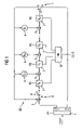
- FIG. 1 shows an apparatus for carrying out a first method with a shift register and an upstream distribution device.
- FIG. 2 shows an apparatus for carrying out a second method with a conventional shift register with the bits being supplied at the front end, and with the allocated coefficients being inverted.
- the decoded bits that are produced by a Viterbi decoder operating on the principle of exact Viterbi traceback, and are produced by the traceback operation for a transport block m occur at the input of the CRC circuit.
- the apparatus according to the invention first of all has a distribution device 1 which is used to distribute the bits between two different outputs D 1 and D 2 .
- the distribution device 1 is supplied with a control signal CTRL in order to switch the signal output between D 1 and D 2 .
- the outputs D 1 and D 2 of the distribution device 1 are respectively connected to the front input and to the rear input of a linear feedback shift register (LFSR) 10 .
- the LFSR 10 carries out a polynomial division process in a manner known per se, in order to check whether the data block has been transmitted correctly.
- the LFSR 10 has a number of memory cells 2 , which store the value arising at the input, and pass on the previously stored value at the output, in each clock step. As is indicated by the dots, further memory cells 2 may be located between the memory cell 2 annotated S 2 and the memory cell 2 which is shown at the right-hand end of the shift register and is annotated S L ⁇ 1 .
- Each memory cell 2 has its own reset input, by means of which, by way of example, all of the memory cells 2 can be set to zero at the start of a processing process.
- Exclusive-OR gates 3 are connected between the memory cells 2 and are used to add the value of the respective upstream memory cell 2 to the output value from the multipliers 4 .
- the value which is applied to the input is multiplied in the multipliers 4 by a coefficient g n from the set ⁇ 0,1 ⁇ , and the product is emitted.
- the coefficients g n correspond to the coefficients in the generator polynomial selected at the transmitter end.
- the memory cells 2 are also connected to an OR gate 5 .
- the CRC circuit also has contact switches 6 and 7 , by means of which a contact between the respective outermost memory cell 2 in the LFSR 10 and the input or output of the LFSR 10 can be made or broken.
- the CRC circuit operates as follows:
- FIG. 2 shows an exemplary embodiment of an apparatus for carrying out the second method according to the invention. This method is used when the bit sequence of the supplied bits is completely inverted with respect to a bit sequence as would be required for the use of a conventional LFSR.
- This apparatus has a linear feedback shift register 20 .
- Exclusive-OR gates 3 are connected between the series-connected memory cells 2 annotated S 0 to S L ⁇ 1 , and their two inputs are respectively connected to the outputs of multipliers 4 and to the outputs of the respective upstream memory cells 2 .
- a feedback line which is connected to the last memory cell S L ⁇ 1 is connected to all of the multipliers 4 .
- the first multiplier 4 is connected to a first exclusive-OR gate 3 , which is connected upstream of the first memory cell 2 and whose second input is supplied with the bit sequence produced by the decoding process.
- the illustrated exemplary embodiment is based on the assumption that the decoding process produces a bit sequence p mL , . . .
- the coefficients are allocated in such a way that the multiplier 4 to which the coefficient g L is applied is connected to the first input-side exclusive-OR gate 3 , and the multiplier 4 to which the coefficient g 1 is applied is connected to the last output-side exclusive-OR gate 3 , and the coefficients in the intermediate processing stages are supplied to the multipliers 4 in the natural sequence of the indices. If this coefficient allocation has not already been preset, it can be changed in the described manner by means of a device which is not illustrated but is connected to the shift register 20 .
- An alternative apparatus which is fundamentally equivalent to the apparatus shown in FIG. 2 , for carrying out the second method on the assumption of a bit sequence produced by the decoding process with a sequence p mL , . . . , p m1 , a mA , . . . , a m1 composed of A payload signal bits and L redundancy checking bits has mirror-image symmetry with the apparatus shown in FIG. 2 , with the bits being entered in an exclusive-OR gate from the right, and with this exclusive-OR gate being connected to the memory cell annotated S L ⁇ 1 . The bits are shifted through the shift register from right to left. On the left-hand side, the feedback line is connected to the output of the memory cell which is annotated S 0 .
- the method according to the invention can be used particularly advantageously in conjunction with a specific 3GPP Standard mode, known as blind transport format detection (BTFD).
- BTFD blind transport format detection
- This mode is based on both the size A of a transport block and the total number M of transport blocks being dynamic variables which can vary between the transmission time intervals (TTI).
- TTI transmission time intervals
Abstract
Description
g CRC8(D)=1+D+D 3 +D 4 +D 7 +D 8, (1)
g CRC12(D)=1+D+D 2 +D 3 +D 11 +D 12, (2)
g CRC16(D)=1+D 5 +D 12 +D 16, (3)
g CRC24(D)=1+D+D 5 +D 6 +D 23 +D 24. (4)
am=(am1, am2, . . . , amA), (5)
systematic CRC coding is carried out in accordance with the Standard mentioned above in such a way that the polynomial
Z m(D)=p mL +p m(L−1) D+ . . . +p m1 D L−1 +a mA D L +a m2 D A+L−2 +a m1 D A+L−1 (6)
has a remainder equal to zero when it is divided by the generator polynomial g(D). The bits in the payload signal vector am and the bits which correspond to the remainder polynomial
p m(D)=p mL +p m(L−1) D+ . . . +p m1 D L−1 (7)
are mapped onto a vector bm as follows:
b m=(b m1 , b m2 , . . . , b m(A+L))=(a m1 , . . . , a mA , p mL , . . . , p m1) (8)
bm=(bm1, bm2, . . . , bm(A+L))=(am1, . . . , amA, pmL, . . . , pm1) (8)
the bits thus appear at the input as a consequence of having been determined, in the reverse time sequence, in the decoder in the sequence pm1, . . . , pmL, amA, . . . , am1.
- 1. First of all, both
contact switches 6 and 7 are placed in the switch position A, so that theLFSR 10 is set up to shift the bits from right to left. - 2. For the first L clock cycles, the
distribution device 1 activates the output D2 and deactivates the output D1, and is controlled appropriately by the control signal CTRL. The CRC parity bits pm1, . . . , pmL thus first of all enter the right-hand input of theLFSR 10 and are passed through theLFSR 10 from right to left. - 3. The contact switches 6 and 7 are then placed in the contact position B, so that the
LFSR 10 is now set up to shift the data bits from left to right. - 4. The output D1 of the
distribution device 1 is then activated, and the output D2 is deactivated, for the next A clock cycles. The information bits amA, . . . , am1 are now shifted into theLFSR 10 from the left-hand side and are shifted from left to right in theLFSR 10, with the feedback line of theLFSR 10 being activated as a result of the contact switch 7 being in the switch position B. Once again, the switching of thedistribution device 1 to the output D1 was initiated by an appropriate control signal ctrl. - 5. Once the information bits have been inserted, the result of the CRC check on the checked data block is available at the output of the OR gate 5.
- 6. If the code block contains more than one transport block, the process starts at 1 again.
Claims (4)
Applications Claiming Priority (3)
| Application Number | Priority Date | Filing Date | Title |
|---|---|---|---|
| DE10238841A DE10238841B4 (en) | 2002-08-23 | 2002-08-23 | Parallel processing of the decoding and the cyclic redundancy check when receiving mobile radio signals |
| DEDE10238841.5 | 2002-08-23 | ||
| PCT/DE2003/002111 WO2004021630A1 (en) | 2002-08-23 | 2003-06-25 | Parallel processing of decoding and of a cyclic redundancy check when mobile radio signals are received |
Related Parent Applications (1)
| Application Number | Title | Priority Date | Filing Date |
|---|---|---|---|
| PCT/DE2003/002111 Continuation WO2004021630A1 (en) | 2002-08-23 | 2003-06-25 | Parallel processing of decoding and of a cyclic redundancy check when mobile radio signals are received |
Publications (2)
| Publication Number | Publication Date |
|---|---|
| US20050229075A1 US20050229075A1 (en) | 2005-10-13 |
| US7461324B2 true US7461324B2 (en) | 2008-12-02 |
Family
ID=31501911
Family Applications (1)
| Application Number | Title | Priority Date | Filing Date |
|---|---|---|---|
| US11/063,949 Expired - Fee Related US7461324B2 (en) | 2002-08-23 | 2005-02-23 | Parallel processing for decoding and cyclic redundancy checking for the reception of mobile radio signals |
Country Status (4)
| Country | Link |
|---|---|
| US (1) | US7461324B2 (en) |
| CN (1) | CN100508440C (en) |
| DE (1) | DE10238841B4 (en) |
| WO (1) | WO2004021630A1 (en) |
Cited By (5)
| Publication number | Priority date | Publication date | Assignee | Title |
|---|---|---|---|---|
| US20080225965A1 (en) * | 2007-03-16 | 2008-09-18 | Zhouyue Pi | Methods and apparatus to improve performance and enable fast decoding of transmissions with multiple code blocks |
| US20090019337A1 (en) * | 2007-07-12 | 2009-01-15 | Zhouyue Pi | Methods and apparatus to compute CRC for multiple code blocks |
| US20090077447A1 (en) * | 2007-09-14 | 2009-03-19 | Motorola, Inc. | Multi-layer cyclic redundancy check code in wireless communication system |
| US20110066926A1 (en) * | 2006-09-27 | 2011-03-17 | Otto Schumacher | Phase shift adjusting method and circuit |
| US20130132796A1 (en) * | 2011-11-21 | 2013-05-23 | Broadcom Corporation | Accelerated Cyclical Redundancy Check |
Families Citing this family (14)
| Publication number | Priority date | Publication date | Assignee | Title |
|---|---|---|---|---|
| US7181671B2 (en) * | 2003-09-23 | 2007-02-20 | Macronix International Co., Ltd. | Parallelized CRC calculation method and system |
| US7712009B2 (en) * | 2005-09-21 | 2010-05-04 | Semiconductor Energy Laboratory Co., Ltd. | Cyclic redundancy check circuit and semiconductor device having the cyclic redundancy check circuit |
| US7802166B2 (en) * | 2006-09-27 | 2010-09-21 | Qimonda Ag | Memory controller, memory circuit and memory system with a memory controller and a memory circuit |
| KR101462211B1 (en) * | 2008-01-30 | 2014-11-17 | 삼성전자주식회사 | Apparatus and method for decoding in portable communication system |
| US7987384B2 (en) * | 2008-02-12 | 2011-07-26 | International Business Machines Corporation | Method, system, and computer program product for handling errors in a cache without processor core recovery |
| CN101854222B (en) * | 2009-03-31 | 2014-04-02 | 华为技术有限公司 | Data processing method, communication device and system |
| US8543888B2 (en) | 2009-06-09 | 2013-09-24 | Microchip Technology Incorporated | Programmable cyclic redundancy check CRC unit |
| CN102006084A (en) * | 2010-09-26 | 2011-04-06 | 东南大学 | CRC (Cyclic Redundancy Check) coding method suitable for OFDM-UWB (Orthogonal Frequency Division Multiplexing- Ultra Wideband) system |
| CN102546089B (en) * | 2011-01-04 | 2014-07-16 | 中兴通讯股份有限公司 | Method and device for implementing cycle redundancy check (CRC) code |
| US9286159B2 (en) * | 2013-11-06 | 2016-03-15 | HGST Netherlands B.V. | Track-band squeezed-sector error correction in magnetic data storage devices |
| US10552258B2 (en) | 2016-09-16 | 2020-02-04 | Semiconductor Energy Laboratory Co., Ltd. | Semiconductor device, electronic device, and driving method thereof |
| US10223194B2 (en) | 2016-11-04 | 2019-03-05 | Semiconductor Energy Laboratory Co., Ltd. | Storage device, semiconductor device, electronic device, and server system |
| TW202032368A (en) * | 2019-02-27 | 2020-09-01 | 智原科技股份有限公司 | Method of executing initial program load applied to electric apparatus |
| EP3939194A4 (en) * | 2019-03-13 | 2022-06-29 | ZTE Corporation | Multi-pilot reference signals |
Citations (11)
| Publication number | Priority date | Publication date | Assignee | Title |
|---|---|---|---|---|
| EP0052357B1 (en) | 1980-11-14 | 1987-04-01 | Nippondenso Co., Ltd. | Ultrasonic detector |
| US5090035A (en) * | 1990-01-19 | 1992-02-18 | Nec Corporation | Linear feedback shift register |
| US5103451A (en) * | 1990-01-29 | 1992-04-07 | Motorola, Inc. | Parallel cyclic redundancy check circuit |
| US5390189A (en) * | 1990-10-01 | 1995-02-14 | Kabushiki Kaisha Toshiba | Semiconductor integrated circuit |
| US5748652A (en) * | 1995-06-29 | 1998-05-05 | Hyundai Electronics Ind. Co., Ltd. | Apparatus for detecting and correcting cyclic redundancy check errors |
| US5920593A (en) * | 1993-11-29 | 1999-07-06 | Dsp Telecommunications Ltd. | Device for personal digital cellular telephones |
| US6041433A (en) * | 1996-01-08 | 2000-03-21 | Matsushita Electric Industrial Co., Ltd. | Viterbi decoder and viterbi decoding method |
| EP1011201A2 (en) | 1998-12-09 | 2000-06-21 | Fujitsu Limited | Error detector, semiconductor device, and error detection method |
| US6327691B1 (en) * | 1999-02-12 | 2001-12-04 | Sony Corporation | System and method for computing and encoding error detection sequences |
| EP1211813A2 (en) | 2000-11-10 | 2002-06-05 | Samsung Electronics Co., Ltd. | Device and method for detecting errors in CRC code having reverse ordered parity bits |
| US7088792B2 (en) * | 1998-03-27 | 2006-08-08 | Lsi Logic Corporation | Device and method for efficient decoding with time reversed data |
Family Cites Families (1)
| Publication number | Priority date | Publication date | Assignee | Title |
|---|---|---|---|---|
| US5390199A (en) * | 1991-07-19 | 1995-02-14 | Anritsu Corporation | Advanced code error detection apparatus and system using maximal-length pseudorandom binary sequence |
-
2002
- 2002-08-23 DE DE10238841A patent/DE10238841B4/en not_active Expired - Fee Related
-
2003
- 2003-06-25 WO PCT/DE2003/002111 patent/WO2004021630A1/en not_active Application Discontinuation
- 2003-06-25 CN CNB038199866A patent/CN100508440C/en not_active Expired - Fee Related
-
2005
- 2005-02-23 US US11/063,949 patent/US7461324B2/en not_active Expired - Fee Related
Patent Citations (11)
| Publication number | Priority date | Publication date | Assignee | Title |
|---|---|---|---|---|
| EP0052357B1 (en) | 1980-11-14 | 1987-04-01 | Nippondenso Co., Ltd. | Ultrasonic detector |
| US5090035A (en) * | 1990-01-19 | 1992-02-18 | Nec Corporation | Linear feedback shift register |
| US5103451A (en) * | 1990-01-29 | 1992-04-07 | Motorola, Inc. | Parallel cyclic redundancy check circuit |
| US5390189A (en) * | 1990-10-01 | 1995-02-14 | Kabushiki Kaisha Toshiba | Semiconductor integrated circuit |
| US5920593A (en) * | 1993-11-29 | 1999-07-06 | Dsp Telecommunications Ltd. | Device for personal digital cellular telephones |
| US5748652A (en) * | 1995-06-29 | 1998-05-05 | Hyundai Electronics Ind. Co., Ltd. | Apparatus for detecting and correcting cyclic redundancy check errors |
| US6041433A (en) * | 1996-01-08 | 2000-03-21 | Matsushita Electric Industrial Co., Ltd. | Viterbi decoder and viterbi decoding method |
| US7088792B2 (en) * | 1998-03-27 | 2006-08-08 | Lsi Logic Corporation | Device and method for efficient decoding with time reversed data |
| EP1011201A2 (en) | 1998-12-09 | 2000-06-21 | Fujitsu Limited | Error detector, semiconductor device, and error detection method |
| US6327691B1 (en) * | 1999-02-12 | 2001-12-04 | Sony Corporation | System and method for computing and encoding error detection sequences |
| EP1211813A2 (en) | 2000-11-10 | 2002-06-05 | Samsung Electronics Co., Ltd. | Device and method for detecting errors in CRC code having reverse ordered parity bits |
Non-Patent Citations (5)
| Title |
|---|
| "4-Bit Bidirectional Universal Shift Register", 54F/74F194, National Semiconductor, Nov. 1994, 7 pgs. |
| "A Reconfigurable Linear Feedback Shift Register (LFSR) for the Bluetooth System", P. Kitsos, N. Sklavos, N. Zervas and O. Koufopavlou, VLSI Design Laboratory, University of Patras, IEEE, vol. 2, Sep. 2, 2001, pp. 991-994. |
| 3<SUP>rd </SUP>Generation Partnership Project (3GPP); Technical Specification Group Radio Access Network Multiplexing and Channel Coding (FDD) (3G TS 25.212 version 3.0.0), XP-002149187, Oct. 1999, 54 pgs. |
| International Search Report, Int'l Application No. PCT/DE03/02111, Int'l Filing Date Jun. 25, 2003, 3 pgs. |
| XP002255882 "Error Control Coding: Fundamentals and Applications", Shu Lin and D.J. Costello, 1987, Prentice Hall, Englewood Cliffs, pp. 98-103. |
Cited By (15)
| Publication number | Priority date | Publication date | Assignee | Title |
|---|---|---|---|---|
| US8909998B2 (en) | 2006-09-27 | 2014-12-09 | Infineon Technologies Ag | Phase shift adjusting method and circuit |
| US20110066926A1 (en) * | 2006-09-27 | 2011-03-17 | Otto Schumacher | Phase shift adjusting method and circuit |
| US8379738B2 (en) | 2007-03-16 | 2013-02-19 | Samsung Electronics Co., Ltd. | Methods and apparatus to improve performance and enable fast decoding of transmissions with multiple code blocks |
| US20080225965A1 (en) * | 2007-03-16 | 2008-09-18 | Zhouyue Pi | Methods and apparatus to improve performance and enable fast decoding of transmissions with multiple code blocks |
| US20090019337A1 (en) * | 2007-07-12 | 2009-01-15 | Zhouyue Pi | Methods and apparatus to compute CRC for multiple code blocks |
| US8862958B2 (en) | 2007-07-12 | 2014-10-14 | Samsung Electronics Co., Ltd. | Methods and apparatus to compute CRC for multiple code blocks |
| US8386878B2 (en) * | 2007-07-12 | 2013-02-26 | Samsung Electronics Co., Ltd. | Methods and apparatus to compute CRC for multiple code blocks |
| US7853857B2 (en) * | 2007-09-14 | 2010-12-14 | Motorola Mobility, Inc. | Multi-layer cyclic redundancy check code in wireless communication system |
| US8327237B2 (en) * | 2007-09-14 | 2012-12-04 | Motorola Mobility Llc | Multi-layer cyclic redundancy check code in wireless communication system |
| US8205143B2 (en) | 2007-09-14 | 2012-06-19 | Motorola Mobility, Inc. | Multi-layer cyclic redundancy check code in wireless communication system |
| US8074150B2 (en) | 2007-09-14 | 2011-12-06 | Motorola Mobility, Inc. | Multi-layer cyclic redundancy check code in wireless communication system |
| US20110066927A1 (en) * | 2007-09-14 | 2011-03-17 | Motorola, Inc. | Multi-layer cyclic reducndancy check code in wireless communication system |
| US20090077447A1 (en) * | 2007-09-14 | 2009-03-19 | Motorola, Inc. | Multi-layer cyclic redundancy check code in wireless communication system |
| US20130132796A1 (en) * | 2011-11-21 | 2013-05-23 | Broadcom Corporation | Accelerated Cyclical Redundancy Check |
| US8856609B2 (en) * | 2011-11-21 | 2014-10-07 | Broadcom Corporation | Accelerated cyclical redundancy check |
Also Published As
| Publication number | Publication date |
|---|---|
| DE10238841A1 (en) | 2004-03-11 |
| CN100508440C (en) | 2009-07-01 |
| US20050229075A1 (en) | 2005-10-13 |
| DE10238841B4 (en) | 2010-01-28 |
| WO2004021630A1 (en) | 2004-03-11 |
| CN1679267A (en) | 2005-10-05 |
Similar Documents
| Publication | Publication Date | Title |
|---|---|---|
| US7461324B2 (en) | Parallel processing for decoding and cyclic redundancy checking for the reception of mobile radio signals | |
| US7246294B2 (en) | Method for iterative hard-decision forward error correction decoding | |
| KR100321978B1 (en) | Apparatus and method for eterative decoding in telecommunication system | |
| EP1655845B1 (en) | Iterative decoding of serial concatenated codes with algebraic decoding of the outer code | |
| US6694478B1 (en) | Low delay channel codes for correcting bursts of lost packets | |
| EP1480366B1 (en) | Error-correcting encoding apparatus | |
| US7577899B2 (en) | Cyclic redundancy check (CRC) based error correction method and device | |
| US20160156432A1 (en) | Signal segmentation method and crc attachment method for reducing undetected error | |
| AU724573B2 (en) | Convolutional decoding with the ending state decided by CRC bits placed inside multiple coding bursts | |
| EP1931034A2 (en) | Error correction method and apparatus for predetermined error patterns | |
| US7657819B2 (en) | Method and apparatus for termination of iterative turbo decoding | |
| JPH08149018A (en) | Error correcting device | |
| CN100547935C (en) | Decoding device and coding/decoding method | |
| MXPA04007076A (en) | Intra-decoder component block messaging. | |
| US5936978A (en) | Shortened fire code error-trapping decoding method and apparatus | |
| US7231575B2 (en) | Apparatus for iterative hard-decision forward error correction decoding | |
| GB2311449A (en) | A variable rate Viterbi decoder for punctuated data | |
| US20060020873A1 (en) | Error correction code generation method and apparatus | |
| US20060090120A1 (en) | Puncturing/depuncturing using compressed differential puncturing pattern | |
| US7219292B2 (en) | Cyclic redundancy check modification for length detection of message with convolutional protection | |
| US6986097B1 (en) | Method and apparatus for generating parity bits in a forward error correction (FEC) system | |
| JP2715398B2 (en) | Error correction codec | |
| EP0981863B1 (en) | Method and apparatus for enhanced performance in a system employing convolutional decoding | |
| Gagnon et al. | Simplified designs for AAPP soft decision threshold decoders | |
| US7155656B1 (en) | Method and system for decoding of binary shortened cyclic code |
Legal Events
| Date | Code | Title | Description |
|---|---|---|---|
| AS | Assignment |
Owner name: INFINEON TECHNOLOGIES AG, GERMANY Free format text: ASSIGNMENT OF ASSIGNORS INTEREST;ASSIGNORS:BERKMANN, JENS;HAAS, WOLFGANG;HERNDL, THOMAS;AND OTHERS;REEL/FRAME:016730/0906;SIGNING DATES FROM 20050415 TO 20050601 |
|
| AS | Assignment |
Owner name: INFINEON TECHNOLOGIES DELTA GMBH, GERMANY Free format text: ASSIGNMENT OF ASSIGNORS INTEREST;ASSIGNOR:INFINEON TECHNOLOGIES AG;REEL/FRAME:026685/0688 Effective date: 19990930 |
|
| AS | Assignment |
Owner name: INFINEON TECHNOLOGIES DELTA GMBH, GERMANY Free format text: CORRECTIVE ASSIGNMENT TO CORRECT THE EFFECTIVE DATE NEEDS TO BE CORRECT TO 09/30/2009 PREVIOUSLY RECORDED ON REEL 026685 FRAME 0688. ASSIGNOR(S) HEREBY CONFIRMS THE ASSIGNMENT;ASSIGNOR:INFINEON TECHNOLOGIES AG;REEL/FRAME:027245/0484 Effective date: 20090930 |
|
| AS | Assignment |
Owner name: INTEL MOBILE COMMUNICATIONS TECHNOLOGY GMBH, GERMA Free format text: ASSIGNMENT OF ASSIGNORS INTEREST;ASSIGNOR:INFINEON TECHNOLOGIES DELTA GMBH;REEL/FRAME:027531/0108 Effective date: 20110131 |
|
| AS | Assignment |
Owner name: INTEL MOBILE COMMUNICATIONS GMBH, GERMANY Free format text: ASSIGNMENT OF ASSIGNORS INTEREST;ASSIGNOR:INTEL MOBILE COMMUNICATIONS TECHNOLOGY GMBH;REEL/FRAME:027556/0709 Effective date: 20111031 |
|
| FPAY | Fee payment |
Year of fee payment: 4 |
|
| AS | Assignment |
Owner name: INTEL DEUTSCHLAND GMBH, GERMANY Free format text: CHANGE OF NAME;ASSIGNOR:INTEL MOBILE COMMUNICATIONS GMBH;REEL/FRAME:037057/0061 Effective date: 20150507 |
|
| REMI | Maintenance fee reminder mailed | ||
| LAPS | Lapse for failure to pay maintenance fees | ||
| STCH | Information on status: patent discontinuation |
Free format text: PATENT EXPIRED DUE TO NONPAYMENT OF MAINTENANCE FEES UNDER 37 CFR 1.362 |
|
| FP | Lapsed due to failure to pay maintenance fee |
Effective date: 20161202 |
|
| AS | Assignment |
Owner name: INTEL CORPORATION, CALIFORNIA Free format text: ASSIGNMENT OF ASSIGNORS INTEREST;ASSIGNOR:INTEL DEUTSCHLAND GMBH;REEL/FRAME:061356/0001 Effective date: 20220708 |