US7432142B2 - Methods of fabricating nitride-based transistors having regrown ohmic contact regions - Google Patents
Methods of fabricating nitride-based transistors having regrown ohmic contact regions Download PDFInfo
- Publication number
- US7432142B2 US7432142B2 US10/849,617 US84961704A US7432142B2 US 7432142 B2 US7432142 B2 US 7432142B2 US 84961704 A US84961704 A US 84961704A US 7432142 B2 US7432142 B2 US 7432142B2
- Authority
- US
- United States
- Prior art keywords
- layer
- contact
- nitride
- forming
- channel layer
- Prior art date
- Legal status (The legal status is an assumption and is not a legal conclusion. Google has not performed a legal analysis and makes no representation as to the accuracy of the status listed.)
- Active, expires
Links
- 150000004767 nitrides Chemical class 0.000 title claims abstract description 130
- 238000000034 method Methods 0.000 title claims abstract description 41
- 230000004888 barrier function Effects 0.000 claims abstract description 93
- 239000000463 material Substances 0.000 claims abstract description 64
- 239000004065 semiconductor Substances 0.000 claims abstract description 39
- 239000000758 substrate Substances 0.000 claims abstract description 26
- 238000004519 manufacturing process Methods 0.000 claims abstract description 24
- 238000005137 deposition process Methods 0.000 claims abstract description 8
- 230000000873 masking effect Effects 0.000 claims description 33
- 229910002704 AlGaN Inorganic materials 0.000 claims description 23
- 229910052751 metal Inorganic materials 0.000 claims description 21
- 239000002184 metal Substances 0.000 claims description 21
- 230000015572 biosynthetic process Effects 0.000 claims description 18
- 229910052581 Si3N4 Inorganic materials 0.000 claims description 14
- HQVNEWCFYHHQES-UHFFFAOYSA-N silicon nitride Chemical compound N12[Si]34N5[Si]62N3[Si]51N64 HQVNEWCFYHHQES-UHFFFAOYSA-N 0.000 claims description 14
- 238000000059 patterning Methods 0.000 claims description 13
- 238000000137 annealing Methods 0.000 claims description 9
- 238000002248 hydride vapour-phase epitaxy Methods 0.000 claims description 9
- 229910052710 silicon Inorganic materials 0.000 claims description 9
- 238000005229 chemical vapour deposition Methods 0.000 claims description 7
- 238000002161 passivation Methods 0.000 claims description 7
- 238000004544 sputter deposition Methods 0.000 claims description 6
- VYPSYNLAJGMNEJ-UHFFFAOYSA-N Silicium dioxide Chemical compound O=[Si]=O VYPSYNLAJGMNEJ-UHFFFAOYSA-N 0.000 claims description 5
- 238000001451 molecular beam epitaxy Methods 0.000 claims description 5
- 230000005533 two-dimensional electron gas Effects 0.000 claims description 4
- 229910052814 silicon oxide Inorganic materials 0.000 claims description 3
- 229920002120 photoresistant polymer Polymers 0.000 claims description 2
- 229910002601 GaN Inorganic materials 0.000 description 31
- HBMJWWWQQXIZIP-UHFFFAOYSA-N silicon carbide Chemical compound [Si+]#[C-] HBMJWWWQQXIZIP-UHFFFAOYSA-N 0.000 description 14
- 238000000151 deposition Methods 0.000 description 13
- 230000008021 deposition Effects 0.000 description 13
- 229910010271 silicon carbide Inorganic materials 0.000 description 13
- IJGRMHOSHXDMSA-UHFFFAOYSA-N Atomic nitrogen Chemical compound N#N IJGRMHOSHXDMSA-UHFFFAOYSA-N 0.000 description 6
- JMASRVWKEDWRBT-UHFFFAOYSA-N Gallium nitride Chemical compound [Ga]#N JMASRVWKEDWRBT-UHFFFAOYSA-N 0.000 description 6
- JBRZTFJDHDCESZ-UHFFFAOYSA-N AsGa Chemical compound [As]#[Ga] JBRZTFJDHDCESZ-UHFFFAOYSA-N 0.000 description 5
- RNQKDQAVIXDKAG-UHFFFAOYSA-N aluminum gallium Chemical compound [Al].[Ga] RNQKDQAVIXDKAG-UHFFFAOYSA-N 0.000 description 5
- 238000001020 plasma etching Methods 0.000 description 5
- 230000007704 transition Effects 0.000 description 5
- 229910001218 Gallium arsenide Inorganic materials 0.000 description 4
- XUIMIQQOPSSXEZ-UHFFFAOYSA-N Silicon Chemical compound [Si] XUIMIQQOPSSXEZ-UHFFFAOYSA-N 0.000 description 4
- 229910052782 aluminium Inorganic materials 0.000 description 4
- XAGFODPZIPBFFR-UHFFFAOYSA-N aluminium Chemical compound [Al] XAGFODPZIPBFFR-UHFFFAOYSA-N 0.000 description 4
- 150000001875 compounds Chemical class 0.000 description 4
- 238000005530 etching Methods 0.000 description 4
- 239000010703 silicon Substances 0.000 description 4
- 230000015556 catabolic process Effects 0.000 description 3
- 239000013078 crystal Substances 0.000 description 3
- 239000002019 doping agent Substances 0.000 description 3
- 238000002513 implantation Methods 0.000 description 3
- 229910052757 nitrogen Inorganic materials 0.000 description 3
- 230000006911 nucleation Effects 0.000 description 3
- 238000010899 nucleation Methods 0.000 description 3
- 229910052594 sapphire Inorganic materials 0.000 description 3
- 239000010980 sapphire Substances 0.000 description 3
- 229910020776 SixNy Inorganic materials 0.000 description 2
- 230000008901 benefit Effects 0.000 description 2
- PMHQVHHXPFUNSP-UHFFFAOYSA-M copper(1+);methylsulfanylmethane;bromide Chemical compound Br[Cu].CSC PMHQVHHXPFUNSP-UHFFFAOYSA-M 0.000 description 2
- 239000003989 dielectric material Substances 0.000 description 2
- 230000005669 field effect Effects 0.000 description 2
- 239000007943 implant Substances 0.000 description 2
- 238000005468 ion implantation Methods 0.000 description 2
- 230000001788 irregular Effects 0.000 description 2
- 238000004518 low pressure chemical vapour deposition Methods 0.000 description 2
- 229910001092 metal group alloy Inorganic materials 0.000 description 2
- 238000000623 plasma-assisted chemical vapour deposition Methods 0.000 description 2
- 230000008569 process Effects 0.000 description 2
- -1 AlInGaN Inorganic materials 0.000 description 1
- GYHNNYVSQQEPJS-UHFFFAOYSA-N Gallium Chemical compound [Ga] GYHNNYVSQQEPJS-UHFFFAOYSA-N 0.000 description 1
- 238000009825 accumulation Methods 0.000 description 1
- 239000000969 carrier Substances 0.000 description 1
- 230000008859 change Effects 0.000 description 1
- 238000005336 cracking Methods 0.000 description 1
- 230000007547 defect Effects 0.000 description 1
- 230000005684 electric field Effects 0.000 description 1
- 229910052733 gallium Inorganic materials 0.000 description 1
- 239000012535 impurity Substances 0.000 description 1
- 229910052738 indium Inorganic materials 0.000 description 1
- APFVFJFRJDLVQX-UHFFFAOYSA-N indium atom Chemical compound [In] APFVFJFRJDLVQX-UHFFFAOYSA-N 0.000 description 1
- 150000002500 ions Chemical class 0.000 description 1
- 238000002955 isolation Methods 0.000 description 1
- 239000000203 mixture Substances 0.000 description 1
- 229910052759 nickel Inorganic materials 0.000 description 1
- TWNQGVIAIRXVLR-UHFFFAOYSA-N oxo(oxoalumanyloxy)alumane Chemical compound O=[Al]O[Al]=O TWNQGVIAIRXVLR-UHFFFAOYSA-N 0.000 description 1
- 229910052763 palladium Inorganic materials 0.000 description 1
- 230000003071 parasitic effect Effects 0.000 description 1
- 230000000737 periodic effect Effects 0.000 description 1
- 229910052697 platinum Inorganic materials 0.000 description 1
- 230000010287 polarization Effects 0.000 description 1
- 238000004886 process control Methods 0.000 description 1
- 230000008439 repair process Effects 0.000 description 1
- 229920006395 saturated elastomer Polymers 0.000 description 1
- 229910021332 silicide Inorganic materials 0.000 description 1
- FVBUAEGBCNSCDD-UHFFFAOYSA-N silicide(4-) Chemical compound [Si-4] FVBUAEGBCNSCDD-UHFFFAOYSA-N 0.000 description 1
- 235000012239 silicon dioxide Nutrition 0.000 description 1
- 239000000377 silicon dioxide Substances 0.000 description 1
- 125000006850 spacer group Chemical group 0.000 description 1
Images


Classifications
-
- H—ELECTRICITY
- H01—ELECTRIC ELEMENTS
- H01L—SEMICONDUCTOR DEVICES NOT COVERED BY CLASS H10
- H01L29/00—Semiconductor devices adapted for rectifying, amplifying, oscillating or switching, or capacitors or resistors with at least one potential-jump barrier or surface barrier, e.g. PN junction depletion layer or carrier concentration layer; Details of semiconductor bodies or of electrodes thereof ; Multistep manufacturing processes therefor
- H01L29/66—Types of semiconductor device ; Multistep manufacturing processes therefor
- H01L29/68—Types of semiconductor device ; Multistep manufacturing processes therefor controllable by only the electric current supplied, or only the electric potential applied, to an electrode which does not carry the current to be rectified, amplified or switched
- H01L29/76—Unipolar devices, e.g. field effect transistors
- H01L29/772—Field effect transistors
- H01L29/778—Field effect transistors with two-dimensional charge carrier gas channel, e.g. HEMT ; with two-dimensional charge-carrier layer formed at a heterojunction interface
- H01L29/7786—Field effect transistors with two-dimensional charge carrier gas channel, e.g. HEMT ; with two-dimensional charge-carrier layer formed at a heterojunction interface with direct single heterostructure, i.e. with wide bandgap layer formed on top of active layer, e.g. direct single heterostructure MIS-like HEMT
- H01L29/7787—Field effect transistors with two-dimensional charge carrier gas channel, e.g. HEMT ; with two-dimensional charge-carrier layer formed at a heterojunction interface with direct single heterostructure, i.e. with wide bandgap layer formed on top of active layer, e.g. direct single heterostructure MIS-like HEMT with wide bandgap charge-carrier supplying layer, e.g. direct single heterostructure MODFET
-
- H—ELECTRICITY
- H01—ELECTRIC ELEMENTS
- H01L—SEMICONDUCTOR DEVICES NOT COVERED BY CLASS H10
- H01L29/00—Semiconductor devices adapted for rectifying, amplifying, oscillating or switching, or capacitors or resistors with at least one potential-jump barrier or surface barrier, e.g. PN junction depletion layer or carrier concentration layer; Details of semiconductor bodies or of electrodes thereof ; Multistep manufacturing processes therefor
- H01L29/66—Types of semiconductor device ; Multistep manufacturing processes therefor
- H01L29/66007—Multistep manufacturing processes
- H01L29/66075—Multistep manufacturing processes of devices having semiconductor bodies comprising group 14 or group 13/15 materials
- H01L29/66227—Multistep manufacturing processes of devices having semiconductor bodies comprising group 14 or group 13/15 materials the devices being controllable only by the electric current supplied or the electric potential applied, to an electrode which does not carry the current to be rectified, amplified or switched, e.g. three-terminal devices
- H01L29/66409—Unipolar field-effect transistors
- H01L29/66446—Unipolar field-effect transistors with an active layer made of a group 13/15 material, e.g. group 13/15 velocity modulation transistor [VMT], group 13/15 negative resistance FET [NERFET]
- H01L29/66454—Static induction transistors [SIT], e.g. permeable base transistors [PBT]
-
- H—ELECTRICITY
- H01—ELECTRIC ELEMENTS
- H01L—SEMICONDUCTOR DEVICES NOT COVERED BY CLASS H10
- H01L29/00—Semiconductor devices adapted for rectifying, amplifying, oscillating or switching, or capacitors or resistors with at least one potential-jump barrier or surface barrier, e.g. PN junction depletion layer or carrier concentration layer; Details of semiconductor bodies or of electrodes thereof ; Multistep manufacturing processes therefor
- H01L29/66—Types of semiconductor device ; Multistep manufacturing processes therefor
- H01L29/68—Types of semiconductor device ; Multistep manufacturing processes therefor controllable by only the electric current supplied, or only the electric potential applied, to an electrode which does not carry the current to be rectified, amplified or switched
- H01L29/76—Unipolar devices, e.g. field effect transistors
- H01L29/772—Field effect transistors
- H01L29/778—Field effect transistors with two-dimensional charge carrier gas channel, e.g. HEMT ; with two-dimensional charge-carrier layer formed at a heterojunction interface
-
- H—ELECTRICITY
- H01—ELECTRIC ELEMENTS
- H01L—SEMICONDUCTOR DEVICES NOT COVERED BY CLASS H10
- H01L29/00—Semiconductor devices adapted for rectifying, amplifying, oscillating or switching, or capacitors or resistors with at least one potential-jump barrier or surface barrier, e.g. PN junction depletion layer or carrier concentration layer; Details of semiconductor bodies or of electrodes thereof ; Multistep manufacturing processes therefor
- H01L29/02—Semiconductor bodies ; Multistep manufacturing processes therefor
- H01L29/12—Semiconductor bodies ; Multistep manufacturing processes therefor characterised by the materials of which they are formed
- H01L29/20—Semiconductor bodies ; Multistep manufacturing processes therefor characterised by the materials of which they are formed including, apart from doping materials or other impurities, only AIIIBV compounds
- H01L29/2003—Nitride compounds
Definitions
- the present invention relates to semiconductor devices and, more particularly, to transistors that incorporate nitride-based active layers.
- the present invention relates to transistors formed of semiconductor materials that can make them suitable for high power, high temperature, and/or high frequency applications.
- Materials such as silicon (Si) and gallium arsenide (GaAs) have found wide application in semiconductor devices for lower power and (in the case of Si) lower frequency applications.
- Si silicon
- GaAs gallium arsenide
- These, more familiar, semiconductor materials may not be well suited for higher power and/or high frequency applications, however, because of their relatively small bandgaps (e.g., 1.12 eV for Si and 1.42 for GaAs at room temperature) and/or relatively small breakdown voltages.
- HEMT High Electron Mobility Transistor
- MODFET modulation doped field effect transistor
- This combination of high carrier concentration and high carrier mobility can give the HEMT a very large transconductance and may provide a strong performance advantage over metal-semiconductor field effect transistors (MESFETs) for high-frequency applications.
- MESFETs metal-semiconductor field effect transistors
- High electron mobility transistors fabricated in the gallium nitride/aluminum gallium nitride (GaN/AlGaN) material system have the potential to generate large amounts of RF power because of the combination of material characteristics that includes the aforementioned high breakdown fields, their wide bandgaps, large conduction band offset, and/or high saturated electron drift velocity.
- a major portion of the electrons in the 2DEG is attributed to polarization in the AlGaN.
- HEMTs in the GaN/AlGaN system have already been demonstrated.
- U.S. Pat. Nos. 5,192,987 and 5,296,395 describe AlGaN/GaN HEMT structures and methods of manufacture.
- ohmic contacts for such transistors.
- ohmic contacts have been formed through reactive ion etching (RIE) recesses for the contacts.
- RIE reactive ion etching
- Ohmic contacts that are formed without RIE have, typically, used high annealing temperatures (e.g. 900° C.). Such high annealing temperatures may damage the materials and/or the device.
- Some embodiments of the present invention provide for fabrication of a transistor including forming a nitride-based channel layer on a substrate, forming a barrier layer on the nitride-based channel layer, forming a contact recess in the barrier layer to expose a contact region of the nitride-based channel layer and forming a contact layer on the exposed contact region of the nitride-based channel layer using a low temperature deposition process. Fabrication may also include forming an ohmic contact on the contact layer and forming a gate contact disposed on the barrier layer adjacent the ohmic contact.
- forming a contact layer on the exposed contact region of the nitride-based channel layer using a low temperature deposition process includes forming a contact layer by metal organic chemical vapor deposition (MOCVD), molecular beam epitaxy (MBE), plasma enchanced chemical vapor deposition (PECVD), sputtering and/or hydride vapor phase epitaxy (HVPE).
- MOCVD metal organic chemical vapor deposition
- MBE molecular beam epitaxy
- PECVD plasma enchanced chemical vapor deposition
- HVPE hydride vapor phase epitaxy
- the low temperature deposition process may be a process other than mass transport from a wafer on which the transistor is formed.
- fabrication of the transistor further includes forming a first dielectric layer on the barrier layer and forming a recess in the first dielectric layer.
- Forming a gate contact includes forming a gate contact in the recess.
- Forming a contact recess includes forming a contact recess in the first dielectric layer and the barrier layer that exposes a portion of the nitride-based channel layer.
- the gate contact may be formed on the first dielectric layer.
- the first dielectric layer comprises a silicon nitride layer.
- the silicon nitride layer may provide a passivation layer for the transistor.
- the contact recess extends into the channel layer.
- forming an ohmic contact may include forming an ohmic contact without annealing the ohmic contact. Forming an ohmic contact could include patterning a metal layer on the contact layer and annealing the patterned metal layer at a temperature of about 850° C. or less.
- forming a contact layer on the exposed portions of the nitride-based channel layer includes forming a contact layer on the exposed portion of the nitride-based channel layer to a thickness sufficient to provide a sheet resistivity of less than a sheet resistivity of a two-dimensional electron gas region formed at an interface between the channel layer and the barrier layer.
- Forming a contact layer may include forming n-type an InGaN, AlInN, AlInGaN and/or InN layer.
- the n-type nitride-based layer formed is GaN and/or AlGaN.
- the InGaN, GaN, AlGaN, AlInN, AlInGaN and/or InN layer may be doped with Si, Ge and/or O during formation.
- the contact layer includes an n-type degenerate semiconductor material other than GaN and AlGaN.
- the contact layer may include a non-nitride Group III-V semiconductor material, a Group IV semiconductor material and/or a group III-VI semiconductor material.
- fabrication of the transistor further includes forming sidewalls of the channel layer to provide an increased surface area interface between the channel layer and the n-type contact layer as compared to a planar interface.
- Forming an ohmic contact on the contact layer may include forming an ohmic contact on the contact layer that extends onto a portion of the channel layer or that terminates before the sidewall of the channel layer.
- fabrication of the transistor includes forming holes in the channel layer adjacent the contact regions and placing n-type nitride-based semiconductor material in the holes. Forming an ohmic contact on the contact layer further includes forming an ohmic contact on the contact layer and on the nitride-based semiconductor material in the holes.
- the contact layer extends onto the barrier layer.
- fabricating a transistor includes forming a nitride-based channel layer on a substrate, forming a barrier layer on the nitride-based channel layer, forming a masking layer on the barrier layer, patterning the masking layer and the barrier layer to provide contact opening that exposes a portion of the nitride-based channel layer, forming a contact layer on the exposed portion of the nitride-based channel layer and the masking layer, selectively removing the masking layer and a portion of the contact layer on the masking layer to provide a contact region, forming an ohmic contact on the contact region and forming a gate contact disposed on the barrier layer adjacent the ohmic contact.
- Fabrication of the transistor may also include forming a first dielectric layer on the barrier layer and forming a recess in the first dielectric layer.
- Forming a gate contact may include forming a gate contact in the recess.
- Forming a masking layer on the barrier layer may include forming a masking layer on the first dielectric layer.
- Patterning the masking layer and the barrier layer to provide contact openings that expose a portion of the nitride-based channel layer may include patterning the masking layer, the first dielectric layer and the barrier layer to provide contact opening that exposes a portion of the nitride-based channel layer.
- the first dielectric layer includes a silicon nitride layer.
- the silicon nitride layer may provide a passivation layer for the transistor.
- the masking layer may be a dielectric layer.
- the dielectric layer may be a silicon oxide layer.
- the masking layer could be a photoresist masking layer.
- Forming an ohmic contact may be provided by forming an ohmic contact without annealing the ohmic contact.
- forming an ohmic contact may be provided by patterning a metal layer on the contact region and annealing the patterned metal layer at a temperature of about 850° C. or less.
- Forming a contact layer on the exposed portion of the nitride-based channel layer and the oxide layer may include forming a contact layer by metal organic chemical vapor deposition (MOCVD), molecular beam epitaxy (MBE), plasma enhanced chemical vapor deposition (PECVD), sputtering and/or hydride vapor phase epitaxy (HVPE).
- MOCVD metal organic chemical vapor deposition
- MBE molecular beam epitaxy
- PECVD plasma enhanced chemical vapor deposition
- HVPE hydride vapor phase epitaxy
- Forming a contact layer on the exposed portions of the nitride-based channel layer and the masking layer may be provided by forming a contact layer on the exposed portions of the nitride-based channel layer and the masking layer to a thickness sufficient to provide a sheet resistivity of less than a sheet resistivity of a two-dimensional electron gas region formed at an interface between the channel layer and the barrier layer.
- Forming a contact layer may include forming an n-type InGaN, AlInGaN, InAlN and/or InN layer.
- the nitride based contact layer may be GaN and/or AlGaN.
- the InGaN, AlInGaN, InAlN, GaN, AlGaN and/or InN layer may be doped with Si, Ge and/or O during formation.
- fabrication of the transistor includes forming sidewalls of the channel layer to provide an increased surface area interface between the channel layer and the n-type contact layer compared to a planar interface.
- Forming an ohmic contact on the contact layer may include forming an ohmic contact on the contact layer that extends onto a portion of the channel layer or that terminates before the sidewall of the channel layer.
- fabrication of the transistor may include forming holes in the channel layer adjacent the contact regions and placing a nitride-based semiconductor material in the holes.
- Forming an ohmic contact on the nitride-based contact region may include forming an ohmic contact on the nitride-based contact region and on the nitride-based semiconductor material in the holes.
- a high electron mobility transistor HEMT
- the HEMT includes a nitride-based channel layer on a substrate, a barrier layer on the nitride-based channel layer, a contact recess in the barrier layer that extends into the channel layer, a contact region on the nitride-based channel layer in the contact recess, a gate contact disposed on the barrier layer.
- the contact region and the nitride-based channel layer include a surface area enlargement structure.
- the surface area enlargement structure includes patterned sidewalls of portions of the contact recess that extends into the channel layer.
- an ohmic contact is provided on the contact region that does not extend onto the channel layer in the area of the sidewalls. In other embodiments of the present invention, the ohmic contact extends onto the channel layer in the area of the sidewalls.
- the surface area enlargement structure includes holes extending into the channel layer with n-type nitride-based semiconductor material in the and the ohmic contact is in contact with the nitride-based semiconductor material in the holes.
- the n-type nitride-based semiconductor material may include InN, AlGaN, InGaN, AlInGaN, AlInN and/or GaN.
- the n-type nitride-based semiconductor material may be doped with Si, Ge and/or O.
- a silicon nitride layer may also be provided on the barrier layer and the gate contact may be provided in a recess in the silicon nitride layer.
- Additional embodiments of the present invention provide a high electron mobility transistor and methods of fabricating a transistor that includes a nitride-based channel layer on a substrate and a barrier layer on the nitride-based channel layer. At least one contact recess is provided in the barrier layer that extends into the channel layer. A region of n-type degenerate semiconductor material other than GaN or AlGaN is provided on the nitride-based channel layer in the contact recess. An ohmic contact is provided on the region of n-type degenerate semiconductor material and a gate contact is disposed on the barrier layer. The region of n-type degenerate semiconductor material may extend onto the barrier layer.
- FIGS. 1A-1G are schematic drawings illustrating fabrication of ohmic contacts in transistors according to embodiments of the present invention.
- FIG. 2 is a schematic illustration of transistors according to further embodiments of the present invention.
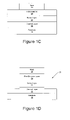
- FIGS. 3A and 3B are schematic illustrations of transistors according to further embodiments of the present invention.
- FIGS. 4A-4C are schematic illustrations of fabrication of transistors according to further embodiments of the present invention.
- first, second, etc. may be used herein to describe various elements, components, regions, layers and/or sections, these elements, components, regions, layers and/or sections should not be limited by these terms. These terms are only used to distinguish one element, component, region, layer or section from another region, layer or section. Thus, a first element, component, region, layer or section discussed below could be termed a second element, component, region, layer or section without departing from the teachings of the present invention.
- relative terms such as “lower” or “bottom” and “upper” or “top,” may be used herein to describe one element's relationship to another elements as illustrated in the Figures. It will be understood that relative terms are intended to encompass different orientations of the device in addition to the orientation depicted in the Figures. For example, if the device in the Figures is turned over, elements described as being on the “lower” side of other elements would then be oriented on “upper” sides of the other elements. The exemplary term “lower”, can therefore, encompasses both an orientation of “lower” and “upper,” depending of the particular orientation of the figure.
- Embodiments of the present invention are described herein with reference to cross-section illustrations that are schematic illustrations of idealized embodiments of the present invention. As such, variations from the shapes of the illustrations as a result, for example, of manufacturing techniques and/or tolerances, are to be expected. Thus, embodiments of the present invention should not be construed as limited to the particular shapes of regions illustrated herein but are to include deviations in shapes that result, for example, from manufacturing. For example, an implanted region illustrated as a rectangle will, typically, have rounded or curved features and/or a gradient of implant concentration at its edges rather than a binary change from implanted to non-implanted region.
- a buried region formed by implantation may result in some implantation in the region between the buried region and the surface through which the implantation takes place.
- the regions illustrated in the figures are schematic in nature and their shapes are not intended to illustrate the precise shape of a region of a device and are not intended to limit the scope of the present invention.
- Embodiments of the present invention provide ohmic contacts on re-grown contact regions of a Group III-nitride based transistor and methods of forming such contacts.
- Embodiments of the present invention may be suited for use in nitride-based HEMTs such as Group III-nitride based devices.
- Group III nitride refers to those semiconducting compounds formed between nitrogen and the elements in Group III of the periodic table, usually aluminum (Al), gallium (Ga), and/or indium (In).
- Al aluminum
- Ga gallium
- In indium
- the term also refers to ternary and quaternary compounds such as AlGaN and AlInGaN.
- the Group III elements can combine with nitrogen to form binary (e.g., GaN), ternary (e.g., AlGaN, AlInN), and quaternary (e.g., AlInGaN) compounds. These compounds all have empirical formulas in which one mole of nitrogen is combined with a total of one mole of the Group III elements. Accordingly, formulas such as Al x Ga 1 ⁇ x N where 0 ⁇ x ⁇ 1 are often used to describe them.
- Suitable structures for GaN-based HEMTs that may utilize embodiments of the present invention are described, for example, in commonly assigned U.S. Pat. No. 6,316,793 and U.S. application Ser. No. 09/904,333 filed Jul. 12, 2001 for “ALUMINUM GALLIUM NITRIDE/GALLIUM NITRIDE HIGH ELECTRON MOBILITY TRANSISTORS HAVING A GATE CONTACT ON A GALLIUM NITRIDE BASED CAP SEGMENT AND METHODS OF FABRICATING SAME,” U.S. provisional application Ser. No.
- FIGS. 1A-1G Fabrication of embodiments of the present invention is schematically illustrated in FIGS. 1A-1G .
- a substrate 10 is provided on which nitride based devices may be formed.
- the substrate 10 may be a semi-insulating silicon carbide (SiC) substrate that may be, for example, 4H polytype of silicon carbide.
- SiC silicon carbide
- Other silicon carbide candidate polytypes include the 3C, 6H, and 15R polytypes.
- the term “semi-insulating” is used descriptively rather than in an absolute sense.
- the silicon carbide bulk crystal has a resistivity equal to or higher than about 1 ⁇ 10 5 ⁇ -cm at room temperature.
- Optional buffer, nucleation and/or transition layers may be provided on the substrate 10 .
- an AlN buffer layer may be provided to provide an appropriate crystal structure transition between the silicon carbide substrate and the remainder of the device.
- strain balancing transition layer(s) may also be provided as described, for example, in commonly assigned U.S. patent application Ser. No. 10/199,786, filed Jul. 19, 2002 and entitled “STRAIN BALANCED NITRIDE HETROJUNCTION TRANSISTORS AND METHODS OF FABRICATING STRAIN BALANCED NITRIDE HETEROJUNCTION TRANSISTORS”, and U.S. Provisional Patent Application Ser. No. 60/337,687, filed Dec. 3, 2001 and entitled “STRAIN BALANCED NITRIDE HETEROJUNCTION TRANSISTOR,” the disclosures of which are incorporated herein by reference as if set forth fully herein.
- Silicon carbide has a much closer crystal lattice match to Group III nitrides than does sapphire (Al 2 O 3 ), which is a very common substrate material for Group III nitride devices. The closer lattice match may result in Group III nitride films of higher quality than those generally available on sapphire. Silicon carbide also has a very high thermal conductivity so that the total output power of Group III nitride devices on silicon carbide is, typically, not as limited by thermal dissipation of the substrate as in the case of the same devices formed on sapphire. Also, the availability of semi-insulating silicon carbide substrates may provide for device isolation and reduced parasitic capacitance.
- SiC substrates are manufactured by, for example, Cree, Inc., of Durham, N.C., the assignee of the present invention, and methods for producing are described, for example, in U.S. Pat. Nos. Re. 34,861; 4,946,547; 5,200,022; and 6,218,680, the contents of which are incorporated herein by reference in their entirety.
- techniques for epitaxial growth of Group III nitrides have been described in, for example, U.S. Pat. Nos. 5,210,051; 5,393,993; 5,523,589; and 5,592,501, the contents of which are also incorporated herein by reference in their entirety.
- silicon carbide may be the preferred substrate material
- embodiments of the present invention may utilize any suitable substrate, such as sapphire, aluminum nitride, aluminum gallium nitride, gallium nitride, silicon, GaAs, LGO, ZnO, LAO, InP and the like.
- an appropriate buffer layer also may be formed.
- a channel layer 20 is provided on the substrate 10 .
- the channel layer 20 may be deposited on the substrate 10 using buffer layers, transition layers, and/or nucleation layers as described above.
- the channel layer 20 may be under compressive strain.
- the channel layer and/or buffer nucleation and/or transition layers may be deposited by MOCVD or by other techniques known to those of skill in the art, such as MBE or HVPE.
- the channel layer 20 is a Group III-nitride, such as Al x Ga 1 ⁇ x N where 0 ⁇ x ⁇ 1, provided that the bandgap of the channel layer 20 is less than the bandgap of the barrier layer 22 .
- the channel layer 20 may also be other Group III-nitrides such as InGaN, AlInGaN or the like.
- the channel layer 20 may be undoped (“unintentionally doped”) and may be grown to a thickness of greater than about 20 ⁇ .
- the channel layer 20 may also be a multi-layer structure, such as a superlattice or combinations of GaN, AlGaN or the like.
- a barrier layer 22 is provided on the channel layer 20 .
- the channel layer 20 may have a bandgap that is less than the bandgap of the barrier layer 22 .
- the barrier layer 22 may be deposited on the channel layer 20 .
- the barrier layer 22 is AlN, AlInN, AlGaN or AlInGaN with a thickness of between about 1 and about 100 nm.
- the barrier layer 22 includes multiple layers.
- the barrier layer 22 may be about 1 nm of AlN with about 25 nm of AlGaN on the AlN layer. Examples of barrier layers according to certain embodiments of the present invention are described in U.S. patent application Ser. No.
- the barrier layer 22 may be a Group III-nitride and has a bandgap larger than that of the channel layer 20 . Accordingly, in certain embodiments of the present invention, the barrier layer 22 is AlGaN, AlInGaN and/or AlN or combinations of layers thereof. Other materials may also be used for the barrier layer 22 . For example, ZnGeN 2 , ZnSiN 2 and/or MgGeN 2 could also be used.
- the barrier layer 22 may, for example, be from about 1 to about 100 mm thick, but is not so thick as to cause cracking or substantial defect formation therein. Preferably, the barrier layer 22 is undoped or doped with an n-type dopant to a concentration less than about 10 19 cm ⁇ 3 .
- the barrier layer 22 is Al x Ga 1 ⁇ x N where 0 ⁇ x ⁇ 1. In such embodiments, the barrier layer 22 may be from about 3 to about 30 nm thick. In particular embodiments, the aluminum concentration is about 25%. However, in other embodiments of the present invention, the barrier layer 22 comprises AlGaN with an aluminum concentration of between about 5% and about 100%. In specific embodiments of the present invention, the aluminum concentration is greater than about 10%. In embodiments of the present invention where the barrier layer 22 comprises an AlN layer, the thickness of the barrier layer 22 may, for example, be from about 0.3 nm to about 4 nm.
- FIG. 1B illustrates formation of an optional first dielectric layer 24 .
- the first dielectric layer 24 may be a silicon nitride layer, such as an Si x N y layer.
- the silicon nitride layer may serve as a passivation layer for the device.
- the silicon nitride layer may be deposited by, for example, plasma-enhanced chemical vapor deposition (PECVD), low pressure chemical vapor deposition (LPCVD) and/or sputtering.
- PECVD plasma-enhanced chemical vapor deposition
- LPCVD low pressure chemical vapor deposition
- sputtering sputtering.
- the silicon nitride layer may be deposited in the same reactor as other layers of the transistor.
- other dielectrics may also be utilized, such as, for example, silicon oxynitride and/or silicon dioxide.
- FIG. 1C illustrates formation of a mask 30 on the first dielectric layer 24 .
- the mask 30 is formed on the region of the barrier layer 22 where a gate contact will subsequently be formed.
- the wafer of FIG. 1C may be removed from the epi reactor and patterned with a mask material 30 to expose the desired recess areas.
- the mask material 30 should be able to withstand the growth temperature of subsequent processing, including the formation of regrown contact regions 26 as described below.
- the mask 30 is provided by an oxide.
- the mask 30 is patterned using lift-off techniques. Alternatively, a wet or dry etch could be utilized to pattern the mask 30 .
- SiO x is the mask material, although other materials, such as AlN and Si x N y based materials, may also be used.
- a photo-resist, e-beam resist material or organic mask material may also be utilized if it is not unduly damaged by subsequent processing steps, such as deposition temperatures or the like.
- the recesses are etched through the first dielectric layer 24 , through the barrier layer 22 , to the channel layer 20 and, in some embodiments, to and into the channel layer 20 or, in some embodiments, even through the channel layer 20 .
- the etch to form the contact recesses 23 may be provided by, for example, a wet etch, a dry etch and/or a reactive ion etch or the like.
- the structure may be annealed to remove and/or reduce damage resulting from the etch.
- the periphery of the device may be etched to form a mesa structure (not shown), for example, if other termination structures, such as a field plate, implant or other termination structure are not provided or may be provided in addition to such structures.
- a contact layer 26 ′ is formed on the exposed regions of the channel layer 20 and the mask 30 .
- the wafer of FIG. 1D may be put back into the epi reactor for deposition of the contact layer 26 ′.
- the contact layer 26 ′ is formed by metal organic chemical vapor deposition (MOCVD), molecular beam epitaxy (MBE), plasma enchanced chemical vapor deposition (PECVD), sputtering and/or hydride vapor phase epitaxy (HVPE).
- MOCVD metal organic chemical vapor deposition
- MBE molecular beam epitaxy
- PECVD plasma enchanced chemical vapor deposition
- HVPE hydride vapor phase epitaxy
- the contact layer 26 ′ is regrown at a reduced deposition temperature. In particular, a low temperature deposition process may be used.
- low temperature deposition refers to formation of a layer at a temperature lower than a temperature at which substantial mass transport from the wafer to the regrown region takes place.
- the contact layer 26 ′ may be formed at a temperature of from about room temperature to about 950° C. In some embodiments, the contact layer 26 ′ is formed at a temperature of less than 960° C. In particular embodiments of the present invention, the contact layer 26 ′ is formed at a very low temperature, for example, at a temperature of less than about 450° C. and in some embodiments, at temperature of less than about 200° C. Such very low temperature conditions may be used, for example, with sputtering and/or PECVD growth techniques. The use of a reduced deposition temperature and/or low temperature deposition may reduce trapping and/or may provide improved reliability.
- the contact layer 26 ′ may be unevenly formed such that the portion on the mask 30 is porous or discontinuous. In some embodiments, the contact layer 26 ′ is not formed on the mask 30 . Such a selective formation of the contact layer 26 ′ may depend on the composition of the contact layer 26 ′, the mask 30 and the growth conditions for the contact layer 26 ′.
- the contact layer 26 ′ may be an n-type degenerate semiconductor material.
- the contact layer 26 ′ may be heavily doped n-type InN, InAlN, AlGaN, AlInGaN, GaN and/or InGaN.
- the contact layer 26 ′ may be an n-type degenerate semiconductor material other than GaN or AlGaN.
- the contact layer may be a non-nitride Group III-V semiconductor material, a Group IV semiconductor material and/or a Group II-VI semiconductor material.
- the contact layer 26 ′ may be a metal or metal alloy, for example, a metal silicide, capable of conformal deposition at a low temperature that has a low work function and does not form a Schottky contact.
- a metal or metal alloy for example, a metal silicide, capable of conformal deposition at a low temperature that has a low work function and does not form a Schottky contact.
- the metal may be subsequently etched off in the channel and gate regions.
- a passivation layer may be deposited before deposition of the metal.
- Formation of a GaN contact layer 26 ′ may reduce and/or eliminate a band discontinuity with the channel layer 22 if the channel layer 22 is also GaN.
- the contact layer 26 ′ is formed to a thickness sufficient to provide a low sheet resistivity.
- the contact layer 26 ′ may be grown to a thickness sufficient to provide a sheet resistivity that is less than a sheet resistivity of the 2DEG formed at the interface between the channel layer 20 and the barrier layer 22 .
- Several tens of nanometers of GaN, for example may be sufficient thickness for the contact layer 26 ′, however, a thicker layer may have a lower resistances and increase transfer length (L T ).
- the contact layer 26 ′ may be doped with Si, Ge and/or O or other suitable n-type dopant or may be naturally n-type as deposited.
- the contact layer 26 ′ may be doped as formed rather than through subsequent ion implantation. Formation of the doped contact layer 26 ′ without ion implantation may avoid the need for extremely high temperature annealing to activate the dopants.
- the contact layer 26 ′ has a sheet resistivity of from about 10 to about 400 ⁇ / ⁇ .
- the contact layer is doped to provide a carrier concentration of from about 10 18 to about 10 21 cm ⁇ 3 .
- the contact layer 26 ′ is from about 10 nm to about 1000 nm thick.
- the mask 30 may not be needed as the material could be blanket deposited and then patterned and etched after deposition.
- FIG. 1F illustrates removal of the portion of the contact layer 26 ′ formed on the mask 30 and removal of the mask 30 to expose the first dielectric layer 24 , thus providing the contact regions 26 .
- the mask 30 and the portion of the contact layer 26 ′ may be removed, for example, by etching the mask 30 in buffered HF or other etchant that will remove the mask layer 30 and leave the first dielectric layer 24 and the contact regions 26 .
- the portion of the contact layer 26 ′ is formed on the mask 30 may be formed so as to be porous or discontinuous so as to allow etching the mask 30 through the contact layer 26 ′.
- the mask 30 may be etched with an etchant that has etching selectivity with respect to the contact layer 26 ′ and the first dielectric layer 24 .
- the mask layer 30 may be etched from the sides to remove the mask layer and the portion of the contact layer 26 ′ on the mask layer 30 , for example, if the portion of the contact layer 26 ′ on the mask layer is not porous or is continuous.
- FIG. 1G illustrates formation of a gate recess in the first dielectric layer 24 and formation of a gate contact 44 on the exposed portion of the barrier layer 22 in the gate recess.
- a gate recess may be etched through the first dielectric layer 24 using, for example, a dry etch, a wet etch and/or RIE or the like.
- the structure may be annealed to repair some or all of the damage resulting from the etch of the gate recess.
- Suitable gate contact materials include, for example, Ni, Pt, Pd or other such Schottky contact materials. Additional overlayers may also be provided.
- the gate contact 44 may be formed on the dielectric layer 24 .
- ohmic contacts 40 and 42 are formed on the contact regions 26 and may provide source and drain contacts.
- the ohmic contacts 40 and 42 may be formed before or after formation of the gate recess and/or contact 44 .
- the ohmic contacts 40 and 42 are annealed, for example at a temperature of about 850° C. or less. In other embodiments, the anneal of the ohmic contacts is not carried out. The use of a reduced anneal temperature or no anneal may reduce trapping and/or may provided improved reliability.
- the presence of the highly doped n-type contact regions may lower contact resistance that may provide for increased efficiency and/or radio frequency power density.
- Suitable ohmic contact materials include, for example, a Ti/Al/Ni/Au stack may be used. Similarly, a structure of Ti/AI/X/Au may be used where X may be Mo, Pt and/or Ti.
- the gate recess and gate contact may be formed before or after formation of the ohmic contacts or even before formation of the contact recesses. Accordingly, embodiments of the present invention should not be construed as limited to the specific sequence of operations described above.
- FIGS. 2 , 3 A and 3 B are illustrations of embodiments of the present invention incorporating contact area enlargement structures that provide increased vertical surface area of the interface between the contact region 26 and the channel layer 20 .
- FIG. 2 illustrates embodiments of the present invention as incorporating a contact area enlargement area structure in a sidewall of a portion of the channel layer 20 and
- FIGS. 3A and 3B illustrate embodiments of the present invention where the contact enlargement area structure is provided by filled holes extending into the contact layer 20 .
- the contact area enlargement structures may also be provided in combination with each other or other structures that increase the vertical contact area between the channel layer 20 and the contact region 26 as compared to a planar vertical contact area.
- Such structures may provide means for increasing a surface area of an interface between a vertical portion of the n-type nitride-based semiconductor material contact region 26 and the nitride-based channel layer 20 .
- FIGS. 2 , 3 A and 3 B illustrate a partial section of a transistor illustrating a single ohmic contact region.
- a corresponding section may be provided for a second ohmic contact region opposite the gate contact so as to provide source and drain contacts.
- embodiments of the present invention may provide a contact area enlargement structure for only one of the ohmic contacts.
- FIG. 2 is a top view of a portion of a HEMT according to further embodiments of the present invention.
- the surface area of the interface between the contact region 26 and the channel layer 20 and/or the barrier layer 22 may be increased by providing an increased surface area sidewall 200 of the channel layer 20 and/or the barrier layer 22 .
- the increased surface area sidewall 200 has an increased surface area with respect to a straight sidewall. Increasing the surface area of the interface between the contact region 26 and the channel layer 20 may reduce the resistance between the contact region 26 and the channel layer 20 .
- the patterned sidewall 200 may be provided by patterning the channel layer 20 during the contact recess etch described above. For example, a first etch through the first dielectric layer 24 and the barrier layer 22 may be performed and then a second etch into the channel layer 22 may be performed with a mask on the exposed portion of the channel layer 20 to provide the pattern of the sidewall. Alternatively, a single etch may be performed if the mask 30 has a pattern corresponding to the desired sidewall pattern of the channel layer 20 .
- the sidewall may have a regular or irregular repeating or non-repeating shape.
- the sawtooth shape illustrated in FIG. 2 is provided as an example of a shape that may be used. However, other shapes may also be used, for example, a notch shape, a series of curves or the like may be used. Accordingly, some embodiments of the present invention should not be limited to a particular shape for the increased surface area sidewall 200 .
- the ohmic contact metal 42 ′ is also illustrated in FIG. 2 on the contact region 26 .
- the contact metal 42 ′ is illustrated as stopping before the periphery of the contact region 26 .
- the contact metal 42 ′ may extend further than illustrated and may, for example, extend onto the channel layer 22 .
- FIG. 3A is a top view and FIG. 3B is a cross-section taken along the lines I-I′ of FIG. 3A of further embodiments of the present invention.
- the surface area of the interface between the regrown contact region 26 and the channel layer 20 may be increased by providing holes 300 that extend into the channel layer 20 .
- the holes 300 have n-type material in them as provided in the contact region 26 .
- the ohmic contact 42 ′′ extends to cover the holes 300 so that the n-type material in the holes 300 is electrically connected to the contact region 26 .
- the filled holes 300 may be provided by patterning the channel layer 20 during the contact recess etch described above so as to provide holes that are present when the contact layer 26 ′ is formed. For example, a first etch through the first dielectric layer 24 and the barrier layer 22 may be performed and then a second etch into the channel layer 22 may be performed with a mask on the exposed portion to the channel layer 20 to provide the holes.
- a single etch may be performed if the mask 30 has a pattern corresponding to the desired holes of the channel layer 20 .
- the holes would extend through the barrier layer 22 and to or into the channel layer 20 .
- the contact metal would then extend onto the barrier layer 22 to contact the material in the holes 300 as illustrated in FIG. 3B .
- the holes 300 may have a regular or irregular repeating or non-repeating pattern. Furthermore, the holes 300 may also have a circular or other shape periphery.
- the pattern of holes and shape of holes illustrated in FIG. 3A is provided as an example of a pattern and shape that may be used. However, other patterns and/or shapes may also be used. Accordingly, some embodiments of the present invention should not be limited to a particular pattern and/or shape for the holes 300 .
- FIGS. 4A-4C illustrate fabrication of further embodiments of the present invention where a contact region is provided that extends onto the barrier layer. Fabrication of the embodiments of the present invention illustrated in FIGS. 4A-4C may be the same as that illustrated in FIGS. 1A-1F except that the first dielectric layer 24 is resized to a smaller size first dielectric layer 424 so as to expose a portion of the barrier layer 22 , for example, by undercutting the mask 30 into the first dielectric layer 24 with an isotropic etch. Alternatively, the mask 30 could be stripped and another mask applied and the first dielectric layer 24 may be etched using this second mask. While the first dielectric layer 424 in FIG. 4A is described herein as a dielectric material, other removable materials that may withstand the conditions for deposition of the contact regions may be used.
- the contact region 426 is regrown as discussed above and the mask 30 is removed.
- the first dielectric layer 424 is removed and a second dielectric layer 430 is conformally deposited on the contact layers 426 and the barrier layer 22 .
- the second dielectric layer 430 would typically be deposited isotropically. Windows in the second dielectric layer 430 may be provided on the contact layer 426 and ohmic contacts for the source and drain contacts 440 and 442 may be formed on the contact layer 426 .
- the ohmic contacts may also be formed prior to the deposition of the second dielectric layer 430 .
- the second dielectric layer 430 is anisotropically etched to expose the barrier layer 22 and provide sidewall spacers 430 ′ and a gate contact recess.
- a gate metal may be deposited and patterned, for example, using lift-off techniques, to provide the gate contact 444 .
- the length of the gate contact 444 may be approximately the width of the first dielectric layer 424 less twice the thickness of the second dielectric layer 430 .
- the first dielectric 424 may have a width of about 0.5 to about 1 ⁇ m and the second dielectric 430 may have a thickness of from about 0.1 to about 0.5 ⁇ m.
- regrown contact regions for both the source and drain contacts
- regrown regions may be provided for only one of the source or the drain.
- the gate contacts have been illustrated as substantially centered between the source and drain, in certain embodiments of the present invention, the gate contact may be offset, for example, toward the source contact.
Abstract
Description
Claims (26)
Priority Applications (8)
| Application Number | Priority Date | Filing Date | Title |
|---|---|---|---|
| US10/849,617 US7432142B2 (en) | 2004-05-20 | 2004-05-20 | Methods of fabricating nitride-based transistors having regrown ohmic contact regions |
| JP2007527194A JP5160225B2 (en) | 2004-05-20 | 2005-02-09 | Method for fabricating nitride-based transistor with regrowth ohmic contact region and nitride-based transistor with regrowth ohmic contact region |
| PCT/US2005/004039 WO2005119787A1 (en) | 2004-05-20 | 2005-02-09 | Methods of fabricating nitride-based transistors having regrown ohmic contact regions and nitride-based transistors having regrown ohmic contact regions |
| EP05722846.2A EP1747589B1 (en) | 2004-05-20 | 2005-02-09 | Methods of fabricating nitride-based transistors having regrown ohmic contact regions and nitride-based transistors having regrown ohmic contact regions |
| CN2005800245027A CN1998085B (en) | 2004-05-20 | 2005-02-09 | Methods of fabricating nitride-based transistors having regrown ohmic contact regions and nitride-based transistors having regrown ohmic contact regions |
| KR1020067026779A KR20070032701A (en) | 2004-05-20 | 2005-02-09 | A method of manufacturing a nitride transistor having a regrown ohmic contact region and a nitride transistor having a regrown ohmic contact region |
| CA002567066A CA2567066A1 (en) | 2004-05-20 | 2005-02-09 | Methods of fabricating nitride-based transistors having regrown ohmic contact regions and nitride-based transistors having regrown ohmic contact regions |
| TW094107182A TW200539264A (en) | 2004-05-20 | 2005-03-09 | Methods of fabricating nitride-based transistors having regrown ohmic contact regions and nitride-based transistors having regrown ohmic contact regions |
Applications Claiming Priority (1)
| Application Number | Priority Date | Filing Date | Title |
|---|---|---|---|
| US10/849,617 US7432142B2 (en) | 2004-05-20 | 2004-05-20 | Methods of fabricating nitride-based transistors having regrown ohmic contact regions |
Publications (2)
| Publication Number | Publication Date |
|---|---|
| US20050258451A1 US20050258451A1 (en) | 2005-11-24 |
| US7432142B2 true US7432142B2 (en) | 2008-10-07 |
Family
ID=34961328
Family Applications (1)
| Application Number | Title | Priority Date | Filing Date |
|---|---|---|---|
| US10/849,617 Active 2024-12-18 US7432142B2 (en) | 2004-05-20 | 2004-05-20 | Methods of fabricating nitride-based transistors having regrown ohmic contact regions |
Country Status (8)
| Country | Link |
|---|---|
| US (1) | US7432142B2 (en) |
| EP (1) | EP1747589B1 (en) |
| JP (1) | JP5160225B2 (en) |
| KR (1) | KR20070032701A (en) |
| CN (1) | CN1998085B (en) |
| CA (1) | CA2567066A1 (en) |
| TW (1) | TW200539264A (en) |
| WO (1) | WO2005119787A1 (en) |
Cited By (46)
| Publication number | Priority date | Publication date | Assignee | Title |
|---|---|---|---|---|
| US20080128753A1 (en) * | 2006-11-30 | 2008-06-05 | Cree, Inc. | Transistors and method for making ohmic contact to transistors |
| US20080173897A1 (en) * | 2007-01-19 | 2008-07-24 | Jianjun Cao | III nitride power device with reduced QGD |
| US20080185608A1 (en) * | 2007-02-01 | 2008-08-07 | Cree, Inc. | Ohmic contacts to nitrogen polarity GaN |
| US20080230786A1 (en) * | 2007-03-23 | 2008-09-25 | Cree, Inc. | High temperature performance capable gallium nitride transistor |
| US20090283787A1 (en) * | 2007-11-14 | 2009-11-19 | Matthew Donofrio | Semiconductor light emitting diodes having reflective structures and methods of fabricating same |
| US20090315078A1 (en) * | 2001-07-24 | 2009-12-24 | Cree, Inc. | INSULATING GATE AlGaN/GaN HEMT |
| US20100025719A1 (en) * | 2008-08-01 | 2010-02-04 | Cree, Inc. | Bond pad design for enhancing light extraction from led chips |
| US20100038682A1 (en) * | 2007-03-30 | 2010-02-18 | Lahreche Hacene | Electronic devices with improved ohmic contact |
| US20100073067A1 (en) * | 2008-09-23 | 2010-03-25 | Transphorm Inc. | Inductive Load Power Switching Circuits |
| US20100109051A1 (en) * | 2006-11-21 | 2010-05-06 | Cree, Inc. | High voltage gan transistors |
| US20100276698A1 (en) * | 2009-04-29 | 2010-11-04 | Cree, Inc. | Gate electrodes for millimeter-wave operation and methods of fabrication |
| US20100320474A1 (en) * | 2009-06-22 | 2010-12-23 | Raytheon Company | Gallium nitride for liquid crystal electrodes |
| US20110215378A1 (en) * | 2010-03-02 | 2011-09-08 | Samsung Electronics Co., Ltd. | High electron mobility transistors exhibiting dual depletion and methods of manufacturing the same |
| US20110217816A1 (en) * | 2007-07-25 | 2011-09-08 | Eudyna Devices Inc. | Field effect transistor and method for fabricating the same |
| US20110241020A1 (en) * | 2010-03-31 | 2011-10-06 | Triquint Semiconductor, Inc. | High electron mobility transistor with recessed barrier layer |
| US8237198B2 (en) | 2008-12-10 | 2012-08-07 | Transphorm Inc. | Semiconductor heterostructure diodes |
| US8390000B2 (en) | 2009-08-28 | 2013-03-05 | Transphorm Inc. | Semiconductor devices with field plates |
| US8389977B2 (en) | 2009-12-10 | 2013-03-05 | Transphorm Inc. | Reverse side engineered III-nitride devices |
| US8519438B2 (en) | 2008-04-23 | 2013-08-27 | Transphorm Inc. | Enhancement mode III-N HEMTs |
| US8598937B2 (en) | 2011-10-07 | 2013-12-03 | Transphorm Inc. | High power semiconductor electronic components with increased reliability |
| US8643062B2 (en) | 2011-02-02 | 2014-02-04 | Transphorm Inc. | III-N device structures and methods |
| US8716141B2 (en) | 2011-03-04 | 2014-05-06 | Transphorm Inc. | Electrode configurations for semiconductor devices |
| US8742459B2 (en) | 2009-05-14 | 2014-06-03 | Transphorm Inc. | High voltage III-nitride semiconductor devices |
| US8742460B2 (en) | 2010-12-15 | 2014-06-03 | Transphorm Inc. | Transistors with isolation regions |
| US8772842B2 (en) | 2011-03-04 | 2014-07-08 | Transphorm, Inc. | Semiconductor diodes with low reverse bias currents |
| US8900985B2 (en) * | 2012-10-15 | 2014-12-02 | Infineon Technologies Austria Ag | Self-doped ohmic contacts for compound semiconductor devices |
| US8901604B2 (en) | 2011-09-06 | 2014-12-02 | Transphorm Inc. | Semiconductor devices with guard rings |
| US9035354B2 (en) | 2004-02-05 | 2015-05-19 | Cree, Inc. | Heterojunction transistors having barrier layer bandgaps greater than channel layer bandgaps and related methods |
| US9054167B2 (en) | 2011-10-26 | 2015-06-09 | Triquint Semiconductor, Inc. | High electron mobility transistor structure and method |
| US9093366B2 (en) | 2012-04-09 | 2015-07-28 | Transphorm Inc. | N-polar III-nitride transistors |
| US9165766B2 (en) | 2012-02-03 | 2015-10-20 | Transphorm Inc. | Buffer layer structures suited for III-nitride devices with foreign substrates |
| US9171730B2 (en) | 2013-02-15 | 2015-10-27 | Transphorm Inc. | Electrodes for semiconductor devices and methods of forming the same |
| US9184275B2 (en) | 2012-06-27 | 2015-11-10 | Transphorm Inc. | Semiconductor devices with integrated hole collectors |
| US9245993B2 (en) | 2013-03-15 | 2016-01-26 | Transphorm Inc. | Carbon doping semiconductor devices |
| US9257547B2 (en) | 2011-09-13 | 2016-02-09 | Transphorm Inc. | III-N device structures having a non-insulating substrate |
| US9318593B2 (en) | 2014-07-21 | 2016-04-19 | Transphorm Inc. | Forming enhancement mode III-nitride devices |
| US9443938B2 (en) | 2013-07-19 | 2016-09-13 | Transphorm Inc. | III-nitride transistor including a p-type depleting layer |
| US9536967B2 (en) | 2014-12-16 | 2017-01-03 | Transphorm Inc. | Recessed ohmic contacts in a III-N device |
| US9536966B2 (en) | 2014-12-16 | 2017-01-03 | Transphorm Inc. | Gate structures for III-N devices |
| US9543490B2 (en) | 2010-09-24 | 2017-01-10 | Seoul Semiconductor Co., Ltd. | Wafer-level light emitting diode package and method of fabricating the same |
| US9590060B2 (en) | 2013-03-13 | 2017-03-07 | Transphorm Inc. | Enhancement-mode III-nitride devices |
| US10224401B2 (en) | 2016-05-31 | 2019-03-05 | Transphorm Inc. | III-nitride devices including a graded depleting layer |
| US10580929B2 (en) | 2016-03-30 | 2020-03-03 | Seoul Viosys Co., Ltd. | UV light emitting diode package and light emitting diode module having the same |
| EP3975224A1 (en) | 2020-09-29 | 2022-03-30 | Valstybinis Moksliniu Tyrimu Institutas Fiziniu Ir Technologijos Mokslu Centras | Method for fabrication of recessed electrical elements |
| US11322599B2 (en) | 2016-01-15 | 2022-05-03 | Transphorm Technology, Inc. | Enhancement mode III-nitride devices having an Al1-xSixO gate insulator |
| WO2022093330A1 (en) | 2020-10-30 | 2022-05-05 | Raytheon Company | Group iii-v semiconductor structures having crystalline regrowth layers and methods for forming such structures |
Families Citing this family (103)
| Publication number | Priority date | Publication date | Assignee | Title |
|---|---|---|---|---|
| KR101288489B1 (en) * | 2002-04-15 | 2013-07-26 | 더 리전츠 오브 더 유니버시티 오브 캘리포니아 | Non-polar (Al,B,In,Ga)N Quantum Well and Heterostructure Materials and Devices |
| US8809867B2 (en) * | 2002-04-15 | 2014-08-19 | The Regents Of The University Of California | Dislocation reduction in non-polar III-nitride thin films |
| JP4889203B2 (en) * | 2004-04-21 | 2012-03-07 | 新日本無線株式会社 | Nitride semiconductor device and manufacturing method thereof |
| US7709859B2 (en) * | 2004-11-23 | 2010-05-04 | Cree, Inc. | Cap layers including aluminum nitride for nitride-based transistors |
| US7456443B2 (en) * | 2004-11-23 | 2008-11-25 | Cree, Inc. | Transistors having buried n-type and p-type regions beneath the source region |
| JP4940557B2 (en) * | 2005-02-08 | 2012-05-30 | 日本電気株式会社 | Field effect transistor and manufacturing method thereof |
| WO2006099138A2 (en) * | 2005-03-10 | 2006-09-21 | The Regents Of The University Of California | Technique for the growth of planar semi-polar gallium nitride |
| US20060226442A1 (en) * | 2005-04-07 | 2006-10-12 | An-Ping Zhang | GaN-based high electron mobility transistor and method for making the same |
| TWI377602B (en) | 2005-05-31 | 2012-11-21 | Japan Science & Tech Agency | Growth of planar non-polar {1-100} m-plane gallium nitride with metalorganic chemical vapor deposition (mocvd) |
| TW200703463A (en) * | 2005-05-31 | 2007-01-16 | Univ California | Defect reduction of non-polar and semi-polar III-nitrides with sidewall lateral epitaxial overgrowth (SLEO) |
| WO2006130696A2 (en) | 2005-06-01 | 2006-12-07 | The Regents Of The University Of California | Technique for the growth and fabrication of semipolar (ga,al,in,b)n thin films, heterostructures, and devices |
| US9331192B2 (en) | 2005-06-29 | 2016-05-03 | Cree, Inc. | Low dislocation density group III nitride layers on silicon carbide substrates and methods of making the same |
| TWI390633B (en) * | 2005-07-13 | 2013-03-21 | Japan Science & Tech Agency | Lateral growth method for defect reduction of semipolar nitride films |
| US20070018198A1 (en) * | 2005-07-20 | 2007-01-25 | Brandes George R | High electron mobility electronic device structures comprising native substrates and methods for making the same |
| TWI404122B (en) * | 2005-09-09 | 2013-08-01 | Univ California | Method for enhancing growth of semi-polar (a1,in,ga,b)n via metalorganic chemical vapor deposition |
| US7338826B2 (en) * | 2005-12-09 | 2008-03-04 | The United States Of America As Represented By The Secretary Of The Navy | Silicon nitride passivation with ammonia plasma pretreatment for improving reliability of AlGaN/GaN HEMTs |
| WO2007084782A2 (en) | 2006-01-20 | 2007-07-26 | The Regents Of The University Of California | Method for improved growth of semipolar (al,in,ga,b)n |
| EP1977441A4 (en) * | 2006-01-20 | 2010-12-01 | Univ California | Method for enhancing growth of semipolar (ai,in,ga,b)n via metalorganic chemical vapor deposition |
| WO2007095137A2 (en) * | 2006-02-10 | 2007-08-23 | The Regents Of The University Of California | Method for conductivity control of (al,in,ga,b)n |
| US7388236B2 (en) * | 2006-03-29 | 2008-06-17 | Cree, Inc. | High efficiency and/or high power density wide bandgap transistors |
| US8764903B2 (en) | 2009-05-05 | 2014-07-01 | Sixpoint Materials, Inc. | Growth reactor for gallium-nitride crystals using ammonia and hydrogen chloride |
| US7723216B2 (en) | 2006-05-09 | 2010-05-25 | The Regents Of The University Of California | In-situ defect reduction techniques for nonpolar and semipolar (Al, Ga, In)N |
| US9040398B2 (en) * | 2006-05-16 | 2015-05-26 | Cree, Inc. | Method of fabricating seminconductor devices including self aligned refractory contacts |
| JP5179023B2 (en) * | 2006-05-31 | 2013-04-10 | パナソニック株式会社 | Field effect transistor |
| US20080078439A1 (en) * | 2006-06-23 | 2008-04-03 | Michael Grundmann | Polarization-induced tunnel junction |
| WO2008021403A2 (en) * | 2006-08-16 | 2008-02-21 | The Regents Of The University Of California | Method for deposition of magnesium doped (al, in, ga, b)n layers |
| US8823057B2 (en) | 2006-11-06 | 2014-09-02 | Cree, Inc. | Semiconductor devices including implanted regions for providing low-resistance contact to buried layers and related devices |
| WO2008060349A2 (en) * | 2006-11-15 | 2008-05-22 | The Regents Of The University Of California | Method for heteroepitaxial growth of high-quality n-face gan, inn, and ain and their alloys by metal organic chemical vapor deposition |
| US8193020B2 (en) | 2006-11-15 | 2012-06-05 | The Regents Of The University Of California | Method for heteroepitaxial growth of high-quality N-face GaN, InN, and AlN and their alloys by metal organic chemical vapor deposition |
| TWI533351B (en) * | 2006-12-11 | 2016-05-11 | 美國加利福尼亞大學董事會 | Metalorganic chemical vapor deposition (mocvd) growth of high performance non-polar iii-nitride optical devices |
| JP2010512660A (en) * | 2006-12-11 | 2010-04-22 | ザ リージェンツ オブ ザ ユニバーシティ オブ カリフォルニア | Nonpolar and semipolar light emitting devices |
| WO2008073414A1 (en) * | 2006-12-12 | 2008-06-19 | The Regents Of The University Of California | Crystal growth of m-plane and semipolar planes of(ai, in, ga, b)n on various substrates |
| JP4876927B2 (en) * | 2007-01-22 | 2012-02-15 | 住友電気工業株式会社 | Method for forming a semiconductor device |
| US8541869B2 (en) * | 2007-02-12 | 2013-09-24 | The Regents Of The University Of California | Cleaved facet (Ga,Al,In)N edge-emitting laser diodes grown on semipolar bulk gallium nitride substrates |
| WO2008100505A1 (en) * | 2007-02-12 | 2008-08-21 | The Regents Of The University Of California | Optimization of laser bar orientation for nonpolar and semipolar (ga,ai,in,b)n diode lasers |
| WO2008112185A1 (en) * | 2007-03-09 | 2008-09-18 | The Regents Of The University Of California | Method to fabricate iii-n field effect transistors using ion implantation with reduced dopant activation and damage recovery temperature |
| US9484499B2 (en) * | 2007-04-20 | 2016-11-01 | Cree, Inc. | Transparent ohmic contacts on light emitting diodes with carrier substrates |
| WO2008137573A1 (en) * | 2007-05-01 | 2008-11-13 | The Regents Of The University Of California | Light emitting diode device layer structure using an indium gallium nitride contact layer |
| TWI339444B (en) | 2007-05-30 | 2011-03-21 | Au Optronics Corp | Conductor structure, pixel structure, and methods of forming the same |
| JP2009010107A (en) * | 2007-06-27 | 2009-01-15 | Oki Electric Ind Co Ltd | Semiconductor device and manufacturing method therefor |
| JP2010536182A (en) * | 2007-08-08 | 2010-11-25 | ザ リージェンツ オブ ザ ユニバーシティ オブ カリフォルニア | Nonpolar III-nitride light emitting diodes with long wavelength radiation |
| JP2010536181A (en) * | 2007-08-08 | 2010-11-25 | ザ リージェンツ オブ ザ ユニバーシティ オブ カリフォルニア | Planar nonpolar M-plane III-nitride thin films grown on miscut substrates |
| US7875537B2 (en) * | 2007-08-29 | 2011-01-25 | Cree, Inc. | High temperature ion implantation of nitride based HEMTs |
| US8080469B2 (en) * | 2007-09-19 | 2011-12-20 | The Regents Of The University Of California | Method for increasing the area of non-polar and semi-polar nitride substrates |
| TWI480435B (en) * | 2007-09-19 | 2015-04-11 | Univ California | Gallium nitride bulk crystals and their growth method |
| JP2010539731A (en) | 2007-09-19 | 2010-12-16 | ザ リージェンツ オブ ザ ユニバーシティ オブ カリフォルニア | (Al, In, Ga, B) N device on patterned substrate |
| US7750370B2 (en) * | 2007-12-20 | 2010-07-06 | Northrop Grumman Space & Mission Systems Corp. | High electron mobility transistor having self-aligned miniature field mitigating plate on a protective dielectric layer |
| JP2011511462A (en) | 2008-02-01 | 2011-04-07 | ザ リージェンツ オブ ザ ユニバーシティ オブ カリフォルニア | Enhanced polarization of nitride light-emitting diodes by off-axis wafer cutting |
| WO2009108700A1 (en) * | 2008-02-25 | 2009-09-03 | Sixpoint Materials, Inc. | Method for producing group iii nitride wafers and group iii nitride wafers |
| US9711633B2 (en) * | 2008-05-09 | 2017-07-18 | Cree, Inc. | Methods of forming group III-nitride semiconductor devices including implanting ions directly into source and drain regions and annealing to activate the implanted ions |
| EP2281076A1 (en) * | 2008-06-04 | 2011-02-09 | Sixpoint Materials, Inc. | Methods for producing improved crystallinty group iii-nitride crystals from initial group iii-nitride seed by ammonothermal growth |
| WO2009149300A1 (en) * | 2008-06-04 | 2009-12-10 | Sixpoint Materials | High-pressure vessel for growing group iii nitride crystals and method of growing group iii nitride crystals using high-pressure vessel and group iii nitride crystal |
| WO2009151642A1 (en) | 2008-06-12 | 2009-12-17 | Sixpoint Materials, Inc. | Method for testing group-iii nitride wafers and group iii-nitride wafers with test data |
| WO2010045567A1 (en) * | 2008-10-16 | 2010-04-22 | Sixpoint Materials, Inc. | Reactor design for growing group iii nitride crystals and method of growing group iii nitride crystals |
| WO2010053964A1 (en) * | 2008-11-07 | 2010-05-14 | The Regents Of The University Of California | Novel vessel designs and relative placements of the source material and seed crystals with respect to the vessel for the ammonothermal growth of group-iii nitride crystals |
| US8852341B2 (en) * | 2008-11-24 | 2014-10-07 | Sixpoint Materials, Inc. | Methods for producing GaN nutrient for ammonothermal growth |
| US8674409B2 (en) | 2008-12-26 | 2014-03-18 | Renesas Electronics Corporation | Heterojunction field effect transistor, method for producing heterojunction field effect transistor, and electronic device |
| US7759142B1 (en) * | 2008-12-31 | 2010-07-20 | Intel Corporation | Quantum well MOSFET channels having uni-axial strain caused by metal source/drains, and conformal regrowth source/drains |
| TW201123530A (en) * | 2009-06-05 | 2011-07-01 | Univ California | Long wavelength nonpolar and semipolar (Al,Ga,In) N based laser diodes |
| JP5580009B2 (en) * | 2009-08-28 | 2014-08-27 | 日本碍子株式会社 | Epitaxial substrate for semiconductor element, semiconductor element, and method for producing epitaxial substrate for semiconductor element |
| JP5609055B2 (en) * | 2009-10-02 | 2014-10-22 | 富士通株式会社 | Compound semiconductor device and manufacturing method thereof |
| US8633470B2 (en) * | 2009-12-23 | 2014-01-21 | Intel Corporation | Techniques and configurations to impart strain to integrated circuit devices |
| US8936976B2 (en) * | 2009-12-23 | 2015-01-20 | Intel Corporation | Conductivity improvements for III-V semiconductor devices |
| US8242510B2 (en) * | 2010-01-28 | 2012-08-14 | Intersil Americas Inc. | Monolithic integration of gallium nitride and silicon devices and circuits, structure and method |
| US9299821B2 (en) * | 2010-06-23 | 2016-03-29 | Cornell University | Gated III-V semiconductor structure and method |
| JP5654884B2 (en) * | 2011-01-26 | 2015-01-14 | 株式会社東芝 | Manufacturing method of nitride semiconductor device |
| US20120204957A1 (en) * | 2011-02-10 | 2012-08-16 | David Nicholls | METHOD FOR GROWING AlInGaN LAYER |
| US8383471B1 (en) * | 2011-04-11 | 2013-02-26 | Hrl Laboratories, Llc | Self aligned sidewall gate GaN HEMT |
| WO2013089843A2 (en) * | 2011-09-02 | 2013-06-20 | The California Institute Of Technology | Photovoltaic semiconductive materials |
| CN103000692A (en) * | 2011-09-14 | 2013-03-27 | 鸿富锦精密工业(深圳)有限公司 | Thin-film transistor structure and manufacturing method thereof |
| US8697505B2 (en) * | 2011-09-15 | 2014-04-15 | Taiwan Semiconductor Manufacturing Company, Ltd. | Method of forming a semiconductor structure |
| US8946771B2 (en) * | 2011-11-09 | 2015-02-03 | Taiwan Semiconductor Manufacturing Co., Ltd. | Gallium nitride semiconductor devices and method making thereof |
| US8884308B2 (en) * | 2011-11-29 | 2014-11-11 | Taiwan Semiconductor Manufacturing Company, Ltd. | High electron mobility transistor structure with improved breakdown voltage performance |
| US9666705B2 (en) * | 2012-05-14 | 2017-05-30 | Infineon Technologies Austria Ag | Contact structures for compound semiconductor devices |
| US9076850B2 (en) | 2012-07-30 | 2015-07-07 | Samsung Electronics Co., Ltd. | High electron mobility transistor |
| US9076763B2 (en) * | 2012-08-13 | 2015-07-07 | Infineon Technologies Austria Ag | High breakdown voltage III-nitride device |
| JP2014045069A (en) * | 2012-08-27 | 2014-03-13 | Toshiba Corp | Semiconductor device and method of manufacturing semiconductor device |
| FR3018629B1 (en) * | 2014-03-14 | 2022-10-28 | Ommic | SEMICONDUCTOR STRUCTURE FORMING TRANSISTOR HEMT |
| CN103928323A (en) * | 2014-03-21 | 2014-07-16 | 中国电子科技集团公司第十三研究所 | Method for reducing ohmic contact resistance of HEMT device |
| CN103903982A (en) * | 2014-03-21 | 2014-07-02 | 中国电子科技集团公司第十三研究所 | Method for reducing ohmic contact resistance of HEMT device |
| CN104393038A (en) * | 2014-10-23 | 2015-03-04 | 西安电子科技大学 | High-breakdown voltage InAlN/AlGaN high-electron mobility transistor and manufacturing method thereof |
| KR101672396B1 (en) * | 2014-11-25 | 2016-11-04 | (재)한국나노기술원 | Quaternary nitride semiconductor power device and manufacturing method thereof |
| USD826871S1 (en) | 2014-12-11 | 2018-08-28 | Cree, Inc. | Light emitting diode device |
| JP6631950B2 (en) * | 2014-12-11 | 2020-01-15 | パナソニックIpマネジメント株式会社 | Nitride semiconductor device and method of manufacturing nitride semiconductor device |
| CN105845680B (en) * | 2015-01-14 | 2019-10-25 | 中芯国际集成电路制造(上海)有限公司 | A kind of semiconductor devices and its manufacturing method and electronic device |
| US20170092747A1 (en) * | 2015-09-30 | 2017-03-30 | Sumitomo Electric Industries, Ltd. | Hemt having heavily doped n-type regions and process of forming the same |
| CN105552108A (en) * | 2015-12-07 | 2016-05-04 | 成都海威华芯科技有限公司 | Forming method of non-alloy ohmic contact of GaN HEMT device |
| JP6690320B2 (en) * | 2016-03-11 | 2020-04-28 | 住友電気工業株式会社 | High electron mobility transistor and method of manufacturing high electron mobility transistor |
| CN107230625A (en) * | 2016-03-25 | 2017-10-03 | 北京大学 | Gallium nitride transistor and its manufacture method |
| CN105789282B (en) * | 2016-04-22 | 2019-01-25 | 西安电子科技大学 | There is one kind part high dopant channel 4H-SiC gold half field effect should manage |
| JP6711233B2 (en) | 2016-10-13 | 2020-06-17 | 富士通株式会社 | Compound semiconductor device and method of manufacturing compound semiconductor device |
| JP7013710B2 (en) * | 2017-08-07 | 2022-02-01 | 住友電気工業株式会社 | Manufacturing method of nitride semiconductor transistor |
| JP6879177B2 (en) * | 2017-11-24 | 2021-06-02 | 住友電気工業株式会社 | Nitride semiconductor device manufacturing method |
| JP7100241B2 (en) * | 2017-12-20 | 2022-07-13 | 富士通株式会社 | Compound semiconductor device and its manufacturing method |
| JP7024534B2 (en) * | 2018-03-20 | 2022-02-24 | 富士通株式会社 | Semiconductor devices and their manufacturing methods |
| CN108598235B (en) * | 2018-05-09 | 2019-12-20 | 芜湖德豪润达光电科技有限公司 | GaN-based LED structure and preparation method thereof |
| TWI714909B (en) * | 2018-11-13 | 2021-01-01 | 新唐科技股份有限公司 | High electron mobility transistor device and manufacturing method thereof |
| JP7417070B2 (en) | 2020-02-06 | 2024-01-18 | 富士通株式会社 | Semiconductor device, semiconductor device manufacturing method, and electronic device |
| GB2594308B (en) * | 2020-04-23 | 2022-06-08 | X Fab Dresden Gmbh & Co Kg | Semiconductor contact structures |
| WO2022124868A1 (en) * | 2020-12-11 | 2022-06-16 | 경북대학교 산학협력단 | High electron mobility transistor and method for manufacturing same |
| US20220376085A1 (en) * | 2021-05-20 | 2022-11-24 | Cree, Inc. | Methods of manufacturing high electron mobility transistors having improved performance |
| US20220376099A1 (en) * | 2021-05-20 | 2022-11-24 | Cree, Inc. | High electron mobility transistors having improved performance |
| CN114005866A (en) * | 2021-09-13 | 2022-02-01 | 西安电子科技大学广州研究院 | GaN high-electron-mobility heterojunction structure, preparation method, diode and transistor |
Citations (72)
| Publication number | Priority date | Publication date | Assignee | Title |
|---|---|---|---|---|
| US4424525A (en) | 1979-12-28 | 1984-01-03 | Fujitsu Limited | High electron mobility single heterojunction semiconductor devices |
| US4471366A (en) | 1979-03-28 | 1984-09-11 | Thomson-Csf | Field effect transistor with high cut-off frequency and process for forming same |
| US4727403A (en) | 1985-04-08 | 1988-02-23 | Nec Corporation | Double heterojunction semiconductor device with injector |
| US4755867A (en) | 1986-08-15 | 1988-07-05 | American Telephone And Telegraph Company, At&T Bell Laboratories | Vertical Enhancement-mode Group III-V compound MISFETs |
| US4788156A (en) | 1986-09-24 | 1988-11-29 | Microwave Technology, Inc. | Subchannel doping to reduce short-gate effects in field effect transistors |
| EP0334006A1 (en) | 1988-02-22 | 1989-09-27 | Siemens Aktiengesellschaft | Stacked channel heterojunction fet |
| US4946547A (en) | 1989-10-13 | 1990-08-07 | Cree Research, Inc. | Method of preparing silicon carbide surfaces for crystal growth |
| US5053348A (en) | 1989-12-01 | 1991-10-01 | Hughes Aircraft Company | Fabrication of self-aligned, t-gate hemt |
| US5140386A (en) * | 1991-05-09 | 1992-08-18 | Raytheon Company | High electron mobility transistor |
| US5172197A (en) | 1990-04-11 | 1992-12-15 | Hughes Aircraft Company | Hemt structure with passivated donor layer |
| US5192987A (en) | 1991-05-17 | 1993-03-09 | Apa Optics, Inc. | High electron mobility transistor with GaN/Alx Ga1-x N heterojunctions |
| US5200022A (en) | 1990-10-03 | 1993-04-06 | Cree Research, Inc. | Method of improving mechanically prepared substrate surfaces of alpha silicon carbide for deposition of beta silicon carbide thereon and resulting product |
| US5210051A (en) | 1990-03-27 | 1993-05-11 | Cree Research, Inc. | High efficiency light emitting diodes from bipolar gallium nitride |
| EP0563847A2 (en) | 1992-03-30 | 1993-10-06 | Matsushita Electric Industrial Co., Ltd. | A field effect transistor |
| WO1993023877A1 (en) | 1992-05-15 | 1993-11-25 | Massachusetts Institute Of Technology | Iii-v based integrated transistor |
| US5292501A (en) | 1990-06-25 | 1994-03-08 | Degenhardt Charles R | Use of a carboxy-substituted polymer to inhibit plaque formation without tooth staining |
| US5298445A (en) | 1992-05-22 | 1994-03-29 | Nec Corporation | Method for fabricating a field effect transistor |
| US5389571A (en) | 1991-12-18 | 1995-02-14 | Hiroshi Amano | Method of fabricating a gallium nitride based semiconductor device with an aluminum and nitrogen containing intermediate layer |
| USRE34861E (en) | 1987-10-26 | 1995-02-14 | North Carolina State University | Sublimation of silicon carbide to produce large, device quality single crystals of silicon carbide |
| US5393993A (en) | 1993-12-13 | 1995-02-28 | Cree Research, Inc. | Buffer structure between silicon carbide and gallium nitride and resulting semiconductor devices |
| US5523589A (en) | 1994-09-20 | 1996-06-04 | Cree Research, Inc. | Vertical geometry light emitting diode with group III nitride active layer and extended lifetime |
| US5534462A (en) | 1995-02-24 | 1996-07-09 | Motorola, Inc. | Method for forming a plug and semiconductor device having the same |
| US5592501A (en) | 1994-09-20 | 1997-01-07 | Cree Research, Inc. | Low-strain laser structures with group III nitride active layers |
| US5686737A (en) | 1994-09-16 | 1997-11-11 | Cree Research, Inc. | Self-aligned field-effect transistor for high frequency applications |
| US5698870A (en) * | 1996-07-22 | 1997-12-16 | The United States Of America As Represented By The Secretary Of The Air Force | High electron mobility transistor (HEMT) and pseudomorphic high electron mobility transistor (PHEMT) devices with single layer integrated metal |
| US5701019A (en) | 1993-03-12 | 1997-12-23 | Hitachi, Ltd. | Semiconductor device having first and second stacked semiconductor layers, with electrical contact to the first semiconductor layer |
| US5700714A (en) | 1995-01-19 | 1997-12-23 | Oki Electric Industry Co., Ltd. | Diffusion mask and fabrication method for forming pn-junction elements in a compound semiconductor substrate |
| US5705827A (en) | 1991-12-25 | 1998-01-06 | Nec Corporation | Tunnel transistor and method of manufacturing same |
| JPH1050982A (en) | 1996-07-31 | 1998-02-20 | Nippon Telegr & Teleph Corp <Ntt> | Semiconductor device |
| US5804482A (en) | 1995-04-10 | 1998-09-08 | Abb Research Ltd. | Method for producing a semiconductor device having a semiconductor layer of SiC |
| US5885860A (en) | 1995-06-30 | 1999-03-23 | Motorola, Inc. | Silicon carbide transistor and method |
| US5946547A (en) | 1995-12-22 | 1999-08-31 | Samsung Electronics Co., Ltd. | Liquid crystal display device fabrication methods with reduced numbers of patterning steps |
| JPH11261053A (en) | 1998-03-09 | 1999-09-24 | Furukawa Electric Co Ltd:The | High electron mobility transistor |
| US5990531A (en) | 1995-12-28 | 1999-11-23 | Philips Electronics N.A. Corporation | Methods of making high voltage GaN-AlN based semiconductor devices and semiconductor devices made |
| US6028328A (en) | 1996-01-03 | 2000-02-22 | Siemens Aktiengesellschaft | HEMT double hetero structure |
| US6046464A (en) | 1995-03-29 | 2000-04-04 | North Carolina State University | Integrated heterostructures of group III-V nitride semiconductor materials including epitaxial ohmic contact comprising multiple quantum well |
| US6064082A (en) | 1997-05-30 | 2000-05-16 | Sony Corporation | Heterojunction field effect transistor |
| US6086673A (en) | 1998-04-02 | 2000-07-11 | Massachusetts Institute Of Technology | Process for producing high-quality III-V nitride substrates |
| US6150680A (en) | 1998-03-05 | 2000-11-21 | Welch Allyn, Inc. | Field effect semiconductor device having dipole barrier |
| US6177685B1 (en) | 1998-01-20 | 2001-01-23 | Sharp Kabushiki Kaisha | Nitride-type III-V HEMT having an InN 2DEG channel layer |
| US6218680B1 (en) | 1999-05-18 | 2001-04-17 | Cree, Inc. | Semi-insulating silicon carbide without vanadium domination |
| WO2001057929A1 (en) | 2000-02-04 | 2001-08-09 | Cree Lighting Company | Group iii nitride based fets and hemts with reduced trapping and method for producing the same |
| US20010015446A1 (en) | 1999-12-08 | 2001-08-23 | Kaoru Inoue | Semiconductor device |
| JP2001230401A (en) | 2000-02-15 | 2001-08-24 | Fuji Film Microdevices Co Ltd | Solid-state image sensing device |
| US20010020700A1 (en) | 2000-01-13 | 2001-09-13 | Kaoru Inoue | Semiconductor device |
| US6316793B1 (en) | 1998-06-12 | 2001-11-13 | Cree, Inc. | Nitride based transistors on semi-insulating silicon carbide substrates |
| US20010040246A1 (en) | 2000-02-18 | 2001-11-15 | Hirotatsu Ishii | GaN field-effect transistor and method of manufacturing the same |
| JP2002016087A (en) | 2000-06-29 | 2002-01-18 | Nec Corp | Semiconductor device |
| US20020008241A1 (en) | 1997-10-07 | 2002-01-24 | Edmond John Adam | Group III nitride photonic devices on silicon carbide substrates with conductive buffer interlayer structure |
| US20020066908A1 (en) | 2000-12-01 | 2002-06-06 | Smith Richard Peter | Aluminum gallium nitride/gallium nitride high electron mobility transistors having a gate contact on a gallium nitride based cap segment and methods of fabricating same |
| US20020079508A1 (en) | 2000-12-19 | 2002-06-27 | The Furukawa Electric Co., Ltd. | GaN-based high electron mobility transistor |
| US6429467B1 (en) | 1999-01-29 | 2002-08-06 | Nec Corporation | Heterojunction field effect transistor |
| US20020119610A1 (en) | 2001-02-27 | 2002-08-29 | Katsunori Nishii | Semiconductor device and method for fabricating the same |
| US6448648B1 (en) | 1997-03-27 | 2002-09-10 | The United States Of America As Represented By The Secretary Of The Navy | Metalization of electronic semiconductor devices |
| US20020167023A1 (en) | 2001-05-11 | 2002-11-14 | Cree Lighting Company And Regents Of The University Of California | Group-III nitride based high electron mobility transistor (HEMT) with barrier/spacer layer |
| US20030017683A1 (en) | 2001-07-18 | 2003-01-23 | Motorola, Inc. | Structure and method for fabricating heterojunction bipolar transistors and high electron mobility transistors utilizing the formation of a complaint substrates for materials used to form the same |
| US20030020092A1 (en) | 2001-07-24 | 2003-01-30 | Primit Parikh | Insulating gate AlGaN/GaN HEMT |
| US6515316B1 (en) | 2000-07-14 | 2003-02-04 | Trw Inc. | Partially relaxed channel HEMT device |
| US6533874B1 (en) * | 1996-12-03 | 2003-03-18 | Advanced Technology Materials, Inc. | GaN-based devices using thick (Ga, Al, In)N base layers |
| US20030102482A1 (en) | 2001-12-03 | 2003-06-05 | Saxler Adam William | Strain balanced nitride heterojunction transistors and methods of fabricating strain balanced nitride heterojunction transistors |
| US20030123829A1 (en) | 1996-10-16 | 2003-07-03 | Taylor Geoff W. | Monolithic integrated circuit including a waveguide and quantum well inversion channel devices and a method of fabricating same |
| US20030145784A1 (en) | 1999-04-08 | 2003-08-07 | Thompson Margarita P. | Cubic (zinc-blende) aluminum nitride and method of making same |
| US20030213975A1 (en) | 2002-05-17 | 2003-11-20 | Matsushita Electric Industrial Co, Ltd. | Semiconductor device |
| US6674101B2 (en) * | 2001-06-01 | 2004-01-06 | Furukawa Electric Co Ltd | GaN-based semiconductor device |
| US20040004223A1 (en) | 1997-01-09 | 2004-01-08 | Nichia Chemical Industries, Ltd. | Nitride semiconductor device |
| WO2004008495A2 (en) | 2002-07-16 | 2004-01-22 | Cree, Inc. | Nitride-based transistors and methods of fabrication thereof using non-etched contact recesses |
| US20040021152A1 (en) | 2002-08-05 | 2004-02-05 | Chanh Nguyen | Ga/A1GaN Heterostructure Field Effect Transistor with dielectric recessed gate |
| US20040029330A1 (en) | 2002-08-05 | 2004-02-12 | Tahir Hussain | Ohmic metal contact and channel protection in GaN devices using an encapsulation layer |
| US6727531B1 (en) * | 2000-08-07 | 2004-04-27 | Advanced Technology Materials, Inc. | Indium gallium nitride channel high electron mobility transistors, and method of making the same |
| US20040241970A1 (en) | 2000-04-11 | 2004-12-02 | Zoltan Ring | Method of Forming Vias in Silicon Carbide and Resulting Devices and Circuits |
| JP2004342810A (en) | 2003-05-15 | 2004-12-02 | Fujitsu Ltd | Compound semiconductor device |
| US6841809B2 (en) * | 2003-04-08 | 2005-01-11 | Sensor Electronic Technology, Inc. | Heterostructure semiconductor device |
Family Cites Families (8)
| Publication number | Priority date | Publication date | Assignee | Title |
|---|---|---|---|---|
| US34861A (en) * | 1862-04-01 | Improved washing-machine | ||
| JP2687897B2 (en) * | 1994-10-13 | 1997-12-08 | 日本電気株式会社 | Field effect transistor and method for manufacturing the same |
| JP3700872B2 (en) * | 1995-12-28 | 2005-09-28 | シャープ株式会社 | Nitride III-V compound semiconductor device and method for manufacturing the same |
| JPH1065213A (en) * | 1996-08-20 | 1998-03-06 | Nichia Chem Ind Ltd | Nitride semiconductor element |
| JP3398613B2 (en) * | 1999-03-15 | 2003-04-21 | 富士通カンタムデバイス株式会社 | Field effect transistor |
| JP2002016312A (en) * | 2000-06-27 | 2002-01-18 | Sanyo Electric Co Ltd | Nitride semiconductor element and its manufacturing method |
| JP3785970B2 (en) * | 2001-09-03 | 2006-06-14 | 日本電気株式会社 | Method for manufacturing group III nitride semiconductor device |
| JP4865189B2 (en) * | 2002-02-21 | 2012-02-01 | 古河電気工業株式会社 | GaN-based field effect transistor |
-
2004
- 2004-05-20 US US10/849,617 patent/US7432142B2/en active Active
-
2005
- 2005-02-09 CN CN2005800245027A patent/CN1998085B/en active Active
- 2005-02-09 JP JP2007527194A patent/JP5160225B2/en active Active
- 2005-02-09 EP EP05722846.2A patent/EP1747589B1/en active Active
- 2005-02-09 WO PCT/US2005/004039 patent/WO2005119787A1/en active Application Filing
- 2005-02-09 KR KR1020067026779A patent/KR20070032701A/en not_active Application Discontinuation
- 2005-02-09 CA CA002567066A patent/CA2567066A1/en not_active Abandoned
- 2005-03-09 TW TW094107182A patent/TW200539264A/en unknown
Patent Citations (83)
| Publication number | Priority date | Publication date | Assignee | Title |
|---|---|---|---|---|
| US4471366A (en) | 1979-03-28 | 1984-09-11 | Thomson-Csf | Field effect transistor with high cut-off frequency and process for forming same |
| US4424525A (en) | 1979-12-28 | 1984-01-03 | Fujitsu Limited | High electron mobility single heterojunction semiconductor devices |
| US4727403A (en) | 1985-04-08 | 1988-02-23 | Nec Corporation | Double heterojunction semiconductor device with injector |
| US4755867A (en) | 1986-08-15 | 1988-07-05 | American Telephone And Telegraph Company, At&T Bell Laboratories | Vertical Enhancement-mode Group III-V compound MISFETs |
| US4788156A (en) | 1986-09-24 | 1988-11-29 | Microwave Technology, Inc. | Subchannel doping to reduce short-gate effects in field effect transistors |
| USRE34861E (en) | 1987-10-26 | 1995-02-14 | North Carolina State University | Sublimation of silicon carbide to produce large, device quality single crystals of silicon carbide |
| EP0334006A1 (en) | 1988-02-22 | 1989-09-27 | Siemens Aktiengesellschaft | Stacked channel heterojunction fet |
| US4946547A (en) | 1989-10-13 | 1990-08-07 | Cree Research, Inc. | Method of preparing silicon carbide surfaces for crystal growth |
| US5053348A (en) | 1989-12-01 | 1991-10-01 | Hughes Aircraft Company | Fabrication of self-aligned, t-gate hemt |
| US5210051A (en) | 1990-03-27 | 1993-05-11 | Cree Research, Inc. | High efficiency light emitting diodes from bipolar gallium nitride |
| US5172197A (en) | 1990-04-11 | 1992-12-15 | Hughes Aircraft Company | Hemt structure with passivated donor layer |
| US5292501A (en) | 1990-06-25 | 1994-03-08 | Degenhardt Charles R | Use of a carboxy-substituted polymer to inhibit plaque formation without tooth staining |
| US5200022A (en) | 1990-10-03 | 1993-04-06 | Cree Research, Inc. | Method of improving mechanically prepared substrate surfaces of alpha silicon carbide for deposition of beta silicon carbide thereon and resulting product |
| US5140386A (en) * | 1991-05-09 | 1992-08-18 | Raytheon Company | High electron mobility transistor |
| US5296395A (en) | 1991-05-17 | 1994-03-22 | Apa Optics, Inc. | Method of making a high electron mobility transistor |
| US5192987A (en) | 1991-05-17 | 1993-03-09 | Apa Optics, Inc. | High electron mobility transistor with GaN/Alx Ga1-x N heterojunctions |
| US5389571A (en) | 1991-12-18 | 1995-02-14 | Hiroshi Amano | Method of fabricating a gallium nitride based semiconductor device with an aluminum and nitrogen containing intermediate layer |
| US5705827A (en) | 1991-12-25 | 1998-01-06 | Nec Corporation | Tunnel transistor and method of manufacturing same |
| EP0563847A2 (en) | 1992-03-30 | 1993-10-06 | Matsushita Electric Industrial Co., Ltd. | A field effect transistor |
| WO1993023877A1 (en) | 1992-05-15 | 1993-11-25 | Massachusetts Institute Of Technology | Iii-v based integrated transistor |
| US5298445A (en) | 1992-05-22 | 1994-03-29 | Nec Corporation | Method for fabricating a field effect transistor |
| US5701019A (en) | 1993-03-12 | 1997-12-23 | Hitachi, Ltd. | Semiconductor device having first and second stacked semiconductor layers, with electrical contact to the first semiconductor layer |
| US5393993A (en) | 1993-12-13 | 1995-02-28 | Cree Research, Inc. | Buffer structure between silicon carbide and gallium nitride and resulting semiconductor devices |
| US5686737A (en) | 1994-09-16 | 1997-11-11 | Cree Research, Inc. | Self-aligned field-effect transistor for high frequency applications |
| US5592501A (en) | 1994-09-20 | 1997-01-07 | Cree Research, Inc. | Low-strain laser structures with group III nitride active layers |
| US5523589A (en) | 1994-09-20 | 1996-06-04 | Cree Research, Inc. | Vertical geometry light emitting diode with group III nitride active layer and extended lifetime |
| US5700714A (en) | 1995-01-19 | 1997-12-23 | Oki Electric Industry Co., Ltd. | Diffusion mask and fabrication method for forming pn-junction elements in a compound semiconductor substrate |
| US5534462A (en) | 1995-02-24 | 1996-07-09 | Motorola, Inc. | Method for forming a plug and semiconductor device having the same |
| US6046464A (en) | 1995-03-29 | 2000-04-04 | North Carolina State University | Integrated heterostructures of group III-V nitride semiconductor materials including epitaxial ohmic contact comprising multiple quantum well |
| US5804482A (en) | 1995-04-10 | 1998-09-08 | Abb Research Ltd. | Method for producing a semiconductor device having a semiconductor layer of SiC |
| US5885860A (en) | 1995-06-30 | 1999-03-23 | Motorola, Inc. | Silicon carbide transistor and method |
| US5946547A (en) | 1995-12-22 | 1999-08-31 | Samsung Electronics Co., Ltd. | Liquid crystal display device fabrication methods with reduced numbers of patterning steps |
| US5990531A (en) | 1995-12-28 | 1999-11-23 | Philips Electronics N.A. Corporation | Methods of making high voltage GaN-AlN based semiconductor devices and semiconductor devices made |
| US6028328A (en) | 1996-01-03 | 2000-02-22 | Siemens Aktiengesellschaft | HEMT double hetero structure |
| US5698870A (en) * | 1996-07-22 | 1997-12-16 | The United States Of America As Represented By The Secretary Of The Air Force | High electron mobility transistor (HEMT) and pseudomorphic high electron mobility transistor (PHEMT) devices with single layer integrated metal |
| JPH1050982A (en) | 1996-07-31 | 1998-02-20 | Nippon Telegr & Teleph Corp <Ntt> | Semiconductor device |
| US20030123829A1 (en) | 1996-10-16 | 2003-07-03 | Taylor Geoff W. | Monolithic integrated circuit including a waveguide and quantum well inversion channel devices and a method of fabricating same |
| US6533874B1 (en) * | 1996-12-03 | 2003-03-18 | Advanced Technology Materials, Inc. | GaN-based devices using thick (Ga, Al, In)N base layers |
| US20040004223A1 (en) | 1997-01-09 | 2004-01-08 | Nichia Chemical Industries, Ltd. | Nitride semiconductor device |
| US6448648B1 (en) | 1997-03-27 | 2002-09-10 | The United States Of America As Represented By The Secretary Of The Navy | Metalization of electronic semiconductor devices |
| US6064082A (en) | 1997-05-30 | 2000-05-16 | Sony Corporation | Heterojunction field effect transistor |
| US20020008241A1 (en) | 1997-10-07 | 2002-01-24 | Edmond John Adam | Group III nitride photonic devices on silicon carbide substrates with conductive buffer interlayer structure |
| US6177685B1 (en) | 1998-01-20 | 2001-01-23 | Sharp Kabushiki Kaisha | Nitride-type III-V HEMT having an InN 2DEG channel layer |
| US6150680A (en) | 1998-03-05 | 2000-11-21 | Welch Allyn, Inc. | Field effect semiconductor device having dipole barrier |
| JPH11261053A (en) | 1998-03-09 | 1999-09-24 | Furukawa Electric Co Ltd:The | High electron mobility transistor |
| US6086673A (en) | 1998-04-02 | 2000-07-11 | Massachusetts Institute Of Technology | Process for producing high-quality III-V nitride substrates |
| US6316793B1 (en) | 1998-06-12 | 2001-11-13 | Cree, Inc. | Nitride based transistors on semi-insulating silicon carbide substrates |
| US6429467B1 (en) | 1999-01-29 | 2002-08-06 | Nec Corporation | Heterojunction field effect transistor |
| US20030145784A1 (en) | 1999-04-08 | 2003-08-07 | Thompson Margarita P. | Cubic (zinc-blende) aluminum nitride and method of making same |
| US6218680B1 (en) | 1999-05-18 | 2001-04-17 | Cree, Inc. | Semi-insulating silicon carbide without vanadium domination |
| US6639255B2 (en) | 1999-12-08 | 2003-10-28 | Matsushita Electric Industrial Co., Ltd. | GaN-based HFET having a surface-leakage reducing cap layer |
| US20010015446A1 (en) | 1999-12-08 | 2001-08-23 | Kaoru Inoue | Semiconductor device |
| US20010020700A1 (en) | 2000-01-13 | 2001-09-13 | Kaoru Inoue | Semiconductor device |
| WO2001057929A1 (en) | 2000-02-04 | 2001-08-09 | Cree Lighting Company | Group iii nitride based fets and hemts with reduced trapping and method for producing the same |
| US20010023964A1 (en) | 2000-02-04 | 2001-09-27 | Yifeng Wu | Group III nitride based FETs and hemts with reduced trapping and method for producing the same |
| US6586781B2 (en) | 2000-02-04 | 2003-07-01 | Cree Lighting Company | Group III nitride based FETs and HEMTs with reduced trapping and method for producing the same |
| JP2001230401A (en) | 2000-02-15 | 2001-08-24 | Fuji Film Microdevices Co Ltd | Solid-state image sensing device |
| US20010040246A1 (en) | 2000-02-18 | 2001-11-15 | Hirotatsu Ishii | GaN field-effect transistor and method of manufacturing the same |
| US20040241970A1 (en) | 2000-04-11 | 2004-12-02 | Zoltan Ring | Method of Forming Vias in Silicon Carbide and Resulting Devices and Circuits |
| JP2002016087A (en) | 2000-06-29 | 2002-01-18 | Nec Corp | Semiconductor device |
| US20020017696A1 (en) | 2000-06-29 | 2002-02-14 | Tatsuo Nakayama | Semiconductor device with schottky electrode having high schottky barrier |
| US6492669B2 (en) | 2000-06-29 | 2002-12-10 | Nec Corporation | Semiconductor device with schottky electrode having high schottky barrier |
| US6515316B1 (en) | 2000-07-14 | 2003-02-04 | Trw Inc. | Partially relaxed channel HEMT device |
| US6727531B1 (en) * | 2000-08-07 | 2004-04-27 | Advanced Technology Materials, Inc. | Indium gallium nitride channel high electron mobility transistors, and method of making the same |
| US6548333B2 (en) | 2000-12-01 | 2003-04-15 | Cree, Inc. | Aluminum gallium nitride/gallium nitride high electron mobility transistors having a gate contact on a gallium nitride based cap segment |
| US20020066908A1 (en) | 2000-12-01 | 2002-06-06 | Smith Richard Peter | Aluminum gallium nitride/gallium nitride high electron mobility transistors having a gate contact on a gallium nitride based cap segment and methods of fabricating same |
| US20030157776A1 (en) | 2000-12-01 | 2003-08-21 | Smith Richard Peter | Methods of fabricating aluminum gallium nitride/gallium nitride high electron mobility transistors having a gate contact on a gallium nitride based cap segment |
| US20020079508A1 (en) | 2000-12-19 | 2002-06-27 | The Furukawa Electric Co., Ltd. | GaN-based high electron mobility transistor |
| US6534801B2 (en) * | 2000-12-19 | 2003-03-18 | The Furukawa Electric Co., Ltd. | GaN-based high electron mobility transistor |
| US20020119610A1 (en) | 2001-02-27 | 2002-08-29 | Katsunori Nishii | Semiconductor device and method for fabricating the same |
| US20020167023A1 (en) | 2001-05-11 | 2002-11-14 | Cree Lighting Company And Regents Of The University Of California | Group-III nitride based high electron mobility transistor (HEMT) with barrier/spacer layer |
| US6674101B2 (en) * | 2001-06-01 | 2004-01-06 | Furukawa Electric Co Ltd | GaN-based semiconductor device |
| US20030017683A1 (en) | 2001-07-18 | 2003-01-23 | Motorola, Inc. | Structure and method for fabricating heterojunction bipolar transistors and high electron mobility transistors utilizing the formation of a complaint substrates for materials used to form the same |
| US20030020092A1 (en) | 2001-07-24 | 2003-01-30 | Primit Parikh | Insulating gate AlGaN/GaN HEMT |
| WO2003049193A1 (en) | 2001-12-03 | 2003-06-12 | Cree, Inc. | Strain balanced nitride heterojunction transistors and methods of fabricating strain balanced nitride heterojunction transistors |
| US20030102482A1 (en) | 2001-12-03 | 2003-06-05 | Saxler Adam William | Strain balanced nitride heterojunction transistors and methods of fabricating strain balanced nitride heterojunction transistors |
| US20030213975A1 (en) | 2002-05-17 | 2003-11-20 | Matsushita Electric Industrial Co, Ltd. | Semiconductor device |
| WO2004008495A2 (en) | 2002-07-16 | 2004-01-22 | Cree, Inc. | Nitride-based transistors and methods of fabrication thereof using non-etched contact recesses |
| US20040061129A1 (en) | 2002-07-16 | 2004-04-01 | Saxler Adam William | Nitride-based transistors and methods of fabrication thereof using non-etched contact recesses |
| US20040021152A1 (en) | 2002-08-05 | 2004-02-05 | Chanh Nguyen | Ga/A1GaN Heterostructure Field Effect Transistor with dielectric recessed gate |
| US20040029330A1 (en) | 2002-08-05 | 2004-02-12 | Tahir Hussain | Ohmic metal contact and channel protection in GaN devices using an encapsulation layer |
| US6841809B2 (en) * | 2003-04-08 | 2005-01-11 | Sensor Electronic Technology, Inc. | Heterostructure semiconductor device |
| JP2004342810A (en) | 2003-05-15 | 2004-12-02 | Fujitsu Ltd | Compound semiconductor device |
Non-Patent Citations (82)
| Title |
|---|
| "Thick AIN template on SiC substrate-Novel semi insulating substrate for GaN-based devices," (C) 2003 by TDI, Inc., http://www.tdii.com/products/AIN<SUB>-</SUB>SiCT.html. |
| Ambacher et al., "Two Dimensional Electron Gases Induced by Spontaneous and Piezoelectric Polarization Charges in N- and Ga-face AlGaN/GaN Heterostructures," Journal of Applied Physics, vol. 85, No. 6, pp. 3222-3233 (Mar. 1999). |
| Ando et al., "10-W/mm AlGaN-GaN HFET With a Field Modulating Plate," IEEE Electron Device Letters, 24(5), pp. 289-291 (May 2003). |
| Asbeck et al. "Piezoelectric charge densities in AlGaN/GaN HFETs," Electronics Letters. vol. 33, No. 14, pp. 1230-1231 (1997). |
| Beaumont, B. et al., "Epitaxial Lateral Overgrowth of GaN," Phys. Stat. Sol. (b) 227, No. 1, pp. 1-43 (2001). |
| Ben-Yaacov et al., "AlGaN/GaN Current Aperture Vertical Electron Transistors with Regrown Channels," Journal of Applied Physics. vol. 95, No. 4, pp. 2073-2078 (2004). |
| Breitschadel et al. "Minimization of Leakage Current of Recessed Gate AlGaN/GaN HEMTs by Optimizing the Dry-Etching Process," Journal of Electronic Materials. vol. 28, No. 12, pp. 1420-1423 (1999). |
| Burm et al. "Recessed Gate GaN MODFETs," Solid-State Electronics. vol. 41, No. 2, pp. 247-250 (1997). |
| Burm et al. "Ultra-Low Resistive Ohmic Contacts on n-GaN Using Si Implantation," Applied Physics Letters. vol. 70, No. 4, 464-66 (1997). |
| Chang et al., "AlGaN/GaN Modulation-Doped Field-Effect Transistors with an Mg-doped Carrier Confinement Layer," Jpn. J. Appl. Phys., 42:3316-3319 (2003). |
| Chen et al. "Cl2 reactive ion etching for gate recessing of AlGaN/GaN field-effect transistors," J. Vac. Sci. Technol. B. vol. 17, No. 6, pp. 2755-2758 (1999). |
| Chini et al., "Power and Linearity Characteristics of Field-Plagted Recessed-Gate AlGaN-GaN HEMTs," IEEE Electron Device Letters, 25(5), pp. 229-231 (May 2004). |
| Cho et al., "A New GaAs Field Effect Transistor (FET) with Dipole Barrier (DIB)," Jpn. J. Appl. Phys. 33:775-778 (1994). |
| Coffie et al., Unpassivated p-GaN/AlGaN/GaN HEMTs with 7.1 W/MMF at 10 GHz, Electronic Letters online No. 20030872, 39(19), (Sep. 18, 2003). |
| Eastman et al. "GaN materials for high power microwave amplifiers," Mat. Res. Soc. Symp. Proc. vol. 512 (1998). |
| Eastman et al. "Undoped AlGaN/GaN HEMTs for Microwave Power Amplification," IEEE Transactions on Electron Devices. vol. 48, No. 3, pp. 479-485 (Mar. 2001). |
| Egawa et al. "Recessed gate ALGaN/GaN MODFET on Sapphire Grown by MOCVD," Applied Physics Letters. vol. 76, No. 1, pp. 121-123 (Jan. 2000). |
| Gaska et al. "Electron Transport in AlGaN/GaN Heterostructures Grown on 6H-SiC Substrates," Applied Physics Letters. vol. 72, No. 6, pp. 707-709 (Feb. 1998). |
| Gaska et al. "High-Temperature Performance on AlGaN/GaN HFET's on SiC Substrates," IEEE Electron Device Letters. vol. 18, No. 1, pp, 492-494 (Oct. 1997). |
| Gaska et al., "Self-Heating in High-Power AlGaN/GaN HFET's," IEEE Electron Device Letters, 19(3), pp. 89-91 (Mar. 1998). |
| Gelmont et al. "Monte Carlo simulation of electron transport in gallium nitride," Journal of Applied Physics. vol. 74, No. 3, pp. 1818-1821 (Aug. 1993). |
| Heikman et al. "Polarization Effects in AlGaN/GaN and GaN/AlGaN/GaN heterostructures," Journal of Applied Physics. vol. 93, No. 12, pp. 10114-10118 (Jun. 2003). |
| Heikman et al., "Growth of Fe-Doped Semi-insulating GaN by Metalorganic Chemical Vapor Deposition," Applied Physics Letters. vol. 83, No. 1, pp. 439-441 (Jul. 2002). |
| Heikman, et al., "Mass Transport Regrowth of GaN for Ohmic Contacts to AlGaN/GaN," Applied Physics Letters. vol. 78, No. 19, pp. 2876. |
| Heikman, Sten K., MOCVD Growth Technologies for Applications in AlGaN/GaN High Electron Mobility Transistors, Dissertation, University of California-Santa Barbara, Sep. 2002, 190 pages. |
| Hikita et al., "350V/150A AlGaN/GaN Power HFET on Silicon Substrate With Source-via Grouding (SVG) Structure," Electron Devices Meeting, 2004, pp. 803-806, IEDM Technical Digest. IEEE International (Dec. 2004). |
| International Search Report corresponding to PCT/US2005/004039, mailed Jun. 30, 2005. |
| Kanaev et al., "Femtosecond and Ultraviolet Laser Irradiation of Graphitelike Hexagonal Boron Nitride," Journal of Applied Physics, 96(8), pp. 4483-4489 (Oct. 15, 2004). |
| Kanamura et al., "A 100-W High-Gain AlGaN/GaN HEMT Power Amplifier on a Conductive N-SiC Substrate for Wireless Base Station Applications," Electron Devices Meeting, 2004, pp. 799-802, IEDM Technical Digest. IEEE International (Dec. 2004). |
| Karmalkar et al. "Enhancement of Breakdown Voltage in AlGaN/GaN High Electron Mobility Transistors Using a Field Plate," IEEETransactions on Electron Devices. vol. 48, No. 8, pp. 1515-1521 (Aug. 2001). |
| Karmalkar et al. "RESURF AlGaN/GaN HEMT for High Voltage Power Switching," IEEE Electron Device Letters. vol. 22, No. 8, pp. 373-375 (Aug, 2001). |
| Karmalkar et al., "Very High Voltage AlGaN/GaN High Electron Mobility Transistors Using a Field Plate Deposited on a Stepped Insulator," Solid State Electronics, vol. 45, pp. 1645-1652 (2001). |
| Kashahara et al., "Ka-ban 2.3W Power AlGan/GaN Heterojunction FET," IEDM Technical Digest, pp. 677-680 (2002). |
| Komiak et al., "Fully Monolithic 4 Watt High Efficiency Ka-band Power Amplifier," IEEE MTT-S International Microwave Symposium Digest, vol. 3, pp. 947-950 (1999). |
| Küsters et al., "Double-Heterojunction Lattice-Matched and Pseudomorphic InGaAs HEMT with delta-Doped InP Supply Layers and p-InP Barier Enhancement Layer Grown by LP-MOVPE," IEEE Electron Device Letters, 14(1), (Jan. 1993). |
| Kuzmik et al. "Annealing of Schottky contacts deposited on dry etched AlGaN/Gan," Semiconductor Science and Technology. vol. 17, No. 11 (Nov. 2002). |
| Manfra et al., "Electron Mobility Exceeding 160 000 cm<SUP>2</SUP>/V s in AlGaN/GaN Heterostructures Grown by Molecular-beam Epitaxy," Applied Physics Letters, 85(22), pp. 5394-5396 (Nov. 29, 2004). |
| Manfra et al., "High Mobility AlGaN/GaN Heterostructures Grown by Plasma-assisted Molecular beam epitaxy on Semi-Insulating GaN Templates Prepared by Hydride Vapor Phase Epitaxy," Journal of Applied Physics, 92(1), pp. 338-345 (Jul. 1, 2002). |
| Manfra et al., "High-Mobility AlGaN/GaN Heterostructures Grown by Molecular-beam Epitaxy on GaN Templates Prepared by Hydride Vapor Phase Epitaxy," Applied Physics Letters, 77(18), pp. 2888-2890 (Oct. 30, 2000). |
| Neuburger et al. "Design of GaN-based Field Effect Transistor Structures based on Doping Screening of Polarization Fields," WA 1.5, 7<SUP>th </SUP>Wide-Gandgap III-Nitride Workship (Mar. 2002). |
| Parikh et al., "Development of Gallium Nitride Epitaxy and Associated Material-Device Correlation for RF, Microwave and MM-wave Applications," Cree, Inc. (35 slides). |
| Ping et al. "DC and Microwave Performance of High-Current AlGaN/GaN Heterostructure Field Effect Transistors Grown on p-Type SiC Substrates," IEEE Electron Device Letters. vol. 19, no. 2, pp. 54-56 (Feb. 1998). |
| Saxler et al., "III-Nitride Heterostructures on High-Purity Semi-Insulating 4H-SiC Substrates for High-Power RF Transistors," International Workshop on Nitride Semiconductors (Jul. 19, 2004). |
| Shen et al., "High-Power Polarization-Engineered GaN/AlGaN/GaN HEMTs Without Surface Passivation," IEEE Electronics Device Letters. vol. 25, No. 1, pp. 7-9 (2004). |
| Sheppard et al. "High Power Demonstration at 10 GHz with GaN/AlGaN HEMT Hybrid Amplifiers." Presented at the 58<SUP>th </SUP>DRC, Denver, CO, Jun. 2000. |
| Sheppard et al. "Improved 10-GHz Operation of GaN/AlGaN HEMTs on Silicon Carbide," Materials Science Forum. vols. 338-342, pp. 1643-1646, (2000). |
| Shiojima et al., "Improved Carrier Confinement by a Buried p-Layer in the AlGaN/GaN HEMT Structure," IEICE Trans. Electron., E83-C(12), (Dec. 2000). |
| Sriram et al. "RF Performance of AlGaN/GaN MODFET's on High Resistivity SiC Substrates," Presentation at Materials Research Society Fall Symposium , 1997. |
| Sriram et al. "SiC and GaN Wide Bandgap Microwave Power Transistors," IEEE Samoff Symposium, Pittsburgh, PA, Mar. 18, 1998. |
| Sullivan et al. "High-Power 10-GHz Operation of AlGaN HFET's on Insulating SiC," IEEE Electron Device Letters. vol. 19, No. 6, pp. 198-200 (Jun. 1998). |
| Tilak et al., "Influence of Barrier Thickness on the High-Power Performance of AlGaN/GaN HEMTs," IEEE Electron Device Letters, 22(1), pp. 504-506 (Nov. 2001). |
| United States Patent Application entitled "Aluminum Free Group III-Nitride Based High Electron Mobility Transistors and Methods of Fabricating Same," U.S. Appl. No. 11/118,575, filed Apr. 29, 2005. |
| United States Patent Application entitled "Binary Group III-Nitride Based High Electron Mobility Transistors and Methods of Fabricating Same," U.S. Appl. No. 11/118,675, filed Apr. 29, 2005. |
| United States Patent Application entitled "Cap Layers and/or Passivation Layers for Nitride-Based Transistors, Transistor Structures and Methods of Fabricating Same," U.S. Appl. No. 10/996,249, filed Nov. 23, 2004. |
| United States Patent Application entitled "Co-Doping for Fermi Level Control in Semi-Insulating Group III Nitrides," filed Jan. 7, 2004. |
| United States Patent Application entitled "Composite Substrates of Conductive And Insulating or Semi-Insulating Group III-Nitrides For Group III-Nitride Devices," U.S. Appl. No. 11/103,127, filed Apr. 11, 2005. |
| United States Patent Application entitled "Field Effect Transistors (FETS) Having Multi-Watt Output Power at Millimeter-Wave Frequencies," U.S. Appl. No. 11/005,423, filed Dec. 6, 2004. |
| United States Patent Application entitled "Group III Nitride Field Effect Transistors (FETs) Capable of Withstanding High Temperature Reverse Bias Test Conditions," U.S. Appl. No. 11/080,905, filed Mar. 15, 2005. |
| United States Patent Application entitled "High Power Density and/or Linearity Transistors," U.S. Appl. No. 11/005,107, filed Dec. 6, 2004. |
| United States Patent Application entitled "Improved Dielectric Passivation for Semiconductor Devices," U.S. Appl. No. 10/851,507, filed May 22, 2004. |
| United States Patent Application entitled "Methods of Fabricating Nitride-Based Transistors with a Cap Layer and a Recessed Gate," filed Jul. 23, 2004. |
| United States Patent Application entitled "Methods of Fabricating Nitride-Based Transistors with a Cap Layer and a Recessed Gate," U.S. Appl. No. 10/897,726, filed Jul. 23, 2004. |
| United States Patent Application entitled "Methods of Having Laterally Grown Active Region and Methods of Fabricating Same," filed Jul. 26, 2004. |
| United States Patent Application entitled "Nitride Heterojunction Transistors Having Charge-Transfer Induced Energy Barriers and Methods of Fabricating the Same," U.S. Appl. No. 10/772,882, filed Feb. 5, 2004. |
| United States Patent Application entitled "Nitride-Based Transistors and Methods of Fabrication Thereof Using Non-Etched Contact Recesses," U.S. Appl. No. 10/617,843, filed Jul. 11, 2003. |
| United States Patent Application entitled "Nitride-Based Transistors with a Protective Layer and a Low-Damage Recess and Methods of Fabrication Thereof," U.S. Appl. No. 10/758,871, filed Jan. 16, 2004. |
| United States Patent Application entitled "Semiconductor Devices Having a Hybrid Channel Layer, Current Aperture Transistors and Methods of Fabricating the Same," U.S. Appl. No. 10/849,589, filed May 20, 2004. |
| United States Patent Application entitled "Silicon Carbide on Diamond Substrates and Related Devices and Methods," U.S. Appl. No. 10/707,898, filed Jan. 22, 2004. |
| United States Patent Application entitled "Thick Semi-Insulating or Insulating Epitaxial Gallium Nitride Layers and Devices Incorporating Same," U.S. Appl. No. 11/103,117, filed Apr. 11, 2005. |
| United States Patent Application entitled, "Silicon Carbide on Diamond Substrates and Related Devices and Methods,". |
| Walker, J. L. B. (Ed.), High Power GaAs FET Amplifiers, Norwood, MA: Artech House, pp. 119-120 (1993). |
| Wu et al. "30-W/mm GaN HEMTs by Field Plate Optimization," IEEE Electron Device Letters. vol. 25, No. 3, pp. 117-119 (Mar. 2004). |
| Wu et al. "High Al-Content AlGaN/GaN MODFET's for Ultrahigh Performance," IEEE Electron Device Letters. vol. 19, No. 2, pp. 50-53 (Feb. 1998). |
| Wu et al., "3.5-Watt AlGaN/GaN HEMTs and Amplifiers at 35 GHz," Cree Santa Barbara Technology Center, Goleta, CA 93117. |
| Wu et al., "3.5-Watt AlGaN/GaN HEMTs and Amplifiers at 35 GHz," IEDM-2003, Cree, Inc. |
| Wu et al., "30-W/mm GaN HEMTs by Field Plate Optimization," IEEE Electron Device Letters, 25(3), pp. 117-119 (Mar. 2004). |
| Wu et al., "Bias-dependent Performance of High-Power AlGaN/GaN HEMTs," IEDM Technical Digest, p. 378-380 (2001). |
| Wu et al., "Linearity Performance of GaN HEMTs With Field Plates," Cree Santa Barbara Technology Center, Goleta, CA 93117. |
| Wu et al., "Linearity Performance of GaN HEMTs With Field Plates," DRC 2004, Cree, Inc. |
| Yu et al. "Schottky barrier engineering in III-V nitrides via the piezoelectric effect," Applied Physics Letters. vol. 73, No. 13, pp. 1880-1882, (Sep. 1998). |
| Yu et al., "Schottky Barrier Engineering in III-V Nitrides via the Piezoelectric Effect," Applied Physics Letters, 73(13), pp. 1880-1882 (Sep. 28, 1998). |
| Zhang et al., "High Breakdown GaN HEMT with Overlapping Gate Structure," IEEE Electron Device Letters, 21(9), pp. 421-423 (Sep. 2000). |
Cited By (113)
| Publication number | Priority date | Publication date | Assignee | Title |
|---|---|---|---|---|
| US9419124B2 (en) | 2001-07-24 | 2016-08-16 | Cree, Inc. | Insulating gate AlGaN/GaN HEMT |
| US10224427B2 (en) | 2001-07-24 | 2019-03-05 | Cree, Inc. | Insulting gate AlGaN/GaN HEMT |
| US20090315078A1 (en) * | 2001-07-24 | 2009-12-24 | Cree, Inc. | INSULATING GATE AlGaN/GaN HEMT |
| US9035354B2 (en) | 2004-02-05 | 2015-05-19 | Cree, Inc. | Heterojunction transistors having barrier layer bandgaps greater than channel layer bandgaps and related methods |
| US7893500B2 (en) | 2006-11-21 | 2011-02-22 | Cree, Inc. | High voltage GaN transistors |
| US20100109051A1 (en) * | 2006-11-21 | 2010-05-06 | Cree, Inc. | High voltage gan transistors |
| US8169005B2 (en) | 2006-11-21 | 2012-05-01 | Cree, Inc. | High voltage GaN transistors |
| US9450081B2 (en) | 2006-11-21 | 2016-09-20 | Cree, Inc. | High voltage GaN transistor |
| US9041064B2 (en) | 2006-11-21 | 2015-05-26 | Cree, Inc. | High voltage GaN transistor |
| US20080128753A1 (en) * | 2006-11-30 | 2008-06-05 | Cree, Inc. | Transistors and method for making ohmic contact to transistors |
| US8878245B2 (en) * | 2006-11-30 | 2014-11-04 | Cree, Inc. | Transistors and method for making ohmic contact to transistors |
| US9076852B2 (en) * | 2007-01-19 | 2015-07-07 | International Rectifier Corporation | III nitride power device with reduced QGD |
| US20080173897A1 (en) * | 2007-01-19 | 2008-07-24 | Jianjun Cao | III nitride power device with reduced QGD |
| US20080185608A1 (en) * | 2007-02-01 | 2008-08-07 | Cree, Inc. | Ohmic contacts to nitrogen polarity GaN |
| US8021904B2 (en) | 2007-02-01 | 2011-09-20 | Cree, Inc. | Ohmic contacts to nitrogen polarity GaN |
| US20080230786A1 (en) * | 2007-03-23 | 2008-09-25 | Cree, Inc. | High temperature performance capable gallium nitride transistor |
| US9240473B2 (en) | 2007-03-23 | 2016-01-19 | Cree, Inc. | High temperature performance capable gallium nitride transistor |
| US8212290B2 (en) | 2007-03-23 | 2012-07-03 | Cree, Inc. | High temperature performance capable gallium nitride transistor |
| US20110215380A1 (en) * | 2007-03-30 | 2011-09-08 | S.O.I.Tec Silicon On Insulator Technologies | Electronic devices with improved ohmic contact |
| US7968390B2 (en) * | 2007-03-30 | 2011-06-28 | S.O.I.Tec Silicon On Insulator Technologies | Electronic devices with improved ohmic contact |
| US20100038682A1 (en) * | 2007-03-30 | 2010-02-18 | Lahreche Hacene | Electronic devices with improved ohmic contact |
| US8253170B2 (en) | 2007-03-30 | 2012-08-28 | Soitec SA & Soitec USA, Inc. | Electronic devices with improved OHMIC contact |
| US20110217816A1 (en) * | 2007-07-25 | 2011-09-08 | Eudyna Devices Inc. | Field effect transistor and method for fabricating the same |
| US8368100B2 (en) | 2007-11-14 | 2013-02-05 | Cree, Inc. | Semiconductor light emitting diodes having reflective structures and methods of fabricating same |
| US20090283787A1 (en) * | 2007-11-14 | 2009-11-19 | Matthew Donofrio | Semiconductor light emitting diodes having reflective structures and methods of fabricating same |
| US9437708B2 (en) | 2008-04-23 | 2016-09-06 | Transphorm Inc. | Enhancement mode III-N HEMTs |
| US9196716B2 (en) | 2008-04-23 | 2015-11-24 | Transphorm Inc. | Enhancement mode III-N HEMTs |
| US9941399B2 (en) | 2008-04-23 | 2018-04-10 | Transphorm Inc. | Enhancement mode III-N HEMTs |
| US8519438B2 (en) | 2008-04-23 | 2013-08-27 | Transphorm Inc. | Enhancement mode III-N HEMTs |
| US8841702B2 (en) | 2008-04-23 | 2014-09-23 | Transphorm Inc. | Enhancement mode III-N HEMTs |
| US20100025719A1 (en) * | 2008-08-01 | 2010-02-04 | Cree, Inc. | Bond pad design for enhancing light extraction from led chips |
| US8384115B2 (en) | 2008-08-01 | 2013-02-26 | Cree, Inc. | Bond pad design for enhancing light extraction from LED chips |
| US8816751B2 (en) | 2008-09-23 | 2014-08-26 | Transphorm Inc. | Inductive load power switching circuits |
| US8531232B2 (en) | 2008-09-23 | 2013-09-10 | Transphorm Inc. | Inductive load power switching circuits |
| US20100073067A1 (en) * | 2008-09-23 | 2010-03-25 | Transphorm Inc. | Inductive Load Power Switching Circuits |
| US9690314B2 (en) | 2008-09-23 | 2017-06-27 | Transphorm Inc. | Inductive load power switching circuits |
| US8493129B2 (en) | 2008-09-23 | 2013-07-23 | Transphorm Inc. | Inductive load power switching circuits |
| US8289065B2 (en) | 2008-09-23 | 2012-10-16 | Transphorm Inc. | Inductive load power switching circuits |
| US9041065B2 (en) | 2008-12-10 | 2015-05-26 | Transphorm Inc. | Semiconductor heterostructure diodes |
| US8237198B2 (en) | 2008-12-10 | 2012-08-07 | Transphorm Inc. | Semiconductor heterostructure diodes |
| US8541818B2 (en) | 2008-12-10 | 2013-09-24 | Transphorm Inc. | Semiconductor heterostructure diodes |
| US20100276698A1 (en) * | 2009-04-29 | 2010-11-04 | Cree, Inc. | Gate electrodes for millimeter-wave operation and methods of fabrication |
| US8741715B2 (en) | 2009-04-29 | 2014-06-03 | Cree, Inc. | Gate electrodes for millimeter-wave operation and methods of fabrication |
| US8742459B2 (en) | 2009-05-14 | 2014-06-03 | Transphorm Inc. | High voltage III-nitride semiconductor devices |
| US9293561B2 (en) | 2009-05-14 | 2016-03-22 | Transphorm Inc. | High voltage III-nitride semiconductor devices |
| US8698200B2 (en) | 2009-06-22 | 2014-04-15 | Raytheon Company | Gallium nitride for liquid crystal electrodes |
| US8268707B2 (en) | 2009-06-22 | 2012-09-18 | Raytheon Company | Gallium nitride for liquid crystal electrodes |
| US20100320474A1 (en) * | 2009-06-22 | 2010-12-23 | Raytheon Company | Gallium nitride for liquid crystal electrodes |
| US9831315B2 (en) | 2009-08-28 | 2017-11-28 | Transphorm Inc. | Semiconductor devices with field plates |
| US8390000B2 (en) | 2009-08-28 | 2013-03-05 | Transphorm Inc. | Semiconductor devices with field plates |
| US8692294B2 (en) | 2009-08-28 | 2014-04-08 | Transphorm Inc. | Semiconductor devices with field plates |
| US9111961B2 (en) | 2009-08-28 | 2015-08-18 | Transphorm Inc. | Semiconductor devices with field plates |
| US9373699B2 (en) | 2009-08-28 | 2016-06-21 | Transphorm Inc. | Semiconductor devices with field plates |
| US9496137B2 (en) | 2009-12-10 | 2016-11-15 | Transphorm Inc. | Methods of forming reverse side engineered III-nitride devices |
| US8389977B2 (en) | 2009-12-10 | 2013-03-05 | Transphorm Inc. | Reverse side engineered III-nitride devices |
| US10199217B2 (en) | 2009-12-10 | 2019-02-05 | Transphorm Inc. | Methods of forming reverse side engineered III-nitride devices |
| US9660048B2 (en) * | 2010-03-02 | 2017-05-23 | Samsung Electronics Co., Ltd. | High electron mobility transistors exhibiting dual depletion and methods of manufacturing the same |
| US20110215378A1 (en) * | 2010-03-02 | 2011-09-08 | Samsung Electronics Co., Ltd. | High electron mobility transistors exhibiting dual depletion and methods of manufacturing the same |
| US20110241020A1 (en) * | 2010-03-31 | 2011-10-06 | Triquint Semiconductor, Inc. | High electron mobility transistor with recessed barrier layer |
| US9543490B2 (en) | 2010-09-24 | 2017-01-10 | Seoul Semiconductor Co., Ltd. | Wafer-level light emitting diode package and method of fabricating the same |
| US9882102B2 (en) | 2010-09-24 | 2018-01-30 | Seoul Semiconductor Co., Ltd. | Wafer-level light emitting diode and wafer-level light emitting diode package |
| US10069048B2 (en) | 2010-09-24 | 2018-09-04 | Seoul Viosys Co., Ltd. | Wafer-level light emitting diode package and method of fabricating the same |
| US10892386B2 (en) | 2010-09-24 | 2021-01-12 | Seoul Semiconductor Co., Ltd. | Wafer-level light emitting diode package and method of fabricating the same |
| US10879437B2 (en) | 2010-09-24 | 2020-12-29 | Seoul Semiconductor Co., Ltd. | Wafer-level light emitting diode package and method of fabricating the same |
| US9147760B2 (en) | 2010-12-15 | 2015-09-29 | Transphorm Inc. | Transistors with isolation regions |
| US9437707B2 (en) | 2010-12-15 | 2016-09-06 | Transphorm Inc. | Transistors with isolation regions |
| US8742460B2 (en) | 2010-12-15 | 2014-06-03 | Transphorm Inc. | Transistors with isolation regions |
| US8895421B2 (en) | 2011-02-02 | 2014-11-25 | Transphorm Inc. | III-N device structures and methods |
| US9224671B2 (en) | 2011-02-02 | 2015-12-29 | Transphorm Inc. | III-N device structures and methods |
| US8643062B2 (en) | 2011-02-02 | 2014-02-04 | Transphorm Inc. | III-N device structures and methods |
| US9142659B2 (en) | 2011-03-04 | 2015-09-22 | Transphorm Inc. | Electrode configurations for semiconductor devices |
| US8772842B2 (en) | 2011-03-04 | 2014-07-08 | Transphorm, Inc. | Semiconductor diodes with low reverse bias currents |
| US8716141B2 (en) | 2011-03-04 | 2014-05-06 | Transphorm Inc. | Electrode configurations for semiconductor devices |
| US8895423B2 (en) | 2011-03-04 | 2014-11-25 | Transphorm Inc. | Method for making semiconductor diodes with low reverse bias currents |
| US9224805B2 (en) | 2011-09-06 | 2015-12-29 | Transphorm Inc. | Semiconductor devices with guard rings |
| US8901604B2 (en) | 2011-09-06 | 2014-12-02 | Transphorm Inc. | Semiconductor devices with guard rings |
| US9257547B2 (en) | 2011-09-13 | 2016-02-09 | Transphorm Inc. | III-N device structures having a non-insulating substrate |
| US8598937B2 (en) | 2011-10-07 | 2013-12-03 | Transphorm Inc. | High power semiconductor electronic components with increased reliability |
| US9171836B2 (en) | 2011-10-07 | 2015-10-27 | Transphorm Inc. | Method of forming electronic components with increased reliability |
| US8860495B2 (en) | 2011-10-07 | 2014-10-14 | Transphorm Inc. | Method of forming electronic components with increased reliability |
| US9054167B2 (en) | 2011-10-26 | 2015-06-09 | Triquint Semiconductor, Inc. | High electron mobility transistor structure and method |
| US9165766B2 (en) | 2012-02-03 | 2015-10-20 | Transphorm Inc. | Buffer layer structures suited for III-nitride devices with foreign substrates |
| US9685323B2 (en) | 2012-02-03 | 2017-06-20 | Transphorm Inc. | Buffer layer structures suited for III-nitride devices with foreign substrates |
| US9093366B2 (en) | 2012-04-09 | 2015-07-28 | Transphorm Inc. | N-polar III-nitride transistors |
| US9490324B2 (en) | 2012-04-09 | 2016-11-08 | Transphorm Inc. | N-polar III-nitride transistors |
| US9634100B2 (en) | 2012-06-27 | 2017-04-25 | Transphorm Inc. | Semiconductor devices with integrated hole collectors |
| US9184275B2 (en) | 2012-06-27 | 2015-11-10 | Transphorm Inc. | Semiconductor devices with integrated hole collectors |
| US8900985B2 (en) * | 2012-10-15 | 2014-12-02 | Infineon Technologies Austria Ag | Self-doped ohmic contacts for compound semiconductor devices |
| US9520491B2 (en) | 2013-02-15 | 2016-12-13 | Transphorm Inc. | Electrodes for semiconductor devices and methods of forming the same |
| US9171730B2 (en) | 2013-02-15 | 2015-10-27 | Transphorm Inc. | Electrodes for semiconductor devices and methods of forming the same |
| US9590060B2 (en) | 2013-03-13 | 2017-03-07 | Transphorm Inc. | Enhancement-mode III-nitride devices |
| US10043898B2 (en) | 2013-03-13 | 2018-08-07 | Transphorm Inc. | Enhancement-mode III-nitride devices |
| US10535763B2 (en) | 2013-03-13 | 2020-01-14 | Transphorm Inc. | Enhancement-mode III-nitride devices |
| US9865719B2 (en) | 2013-03-15 | 2018-01-09 | Transphorm Inc. | Carbon doping semiconductor devices |
| US9245993B2 (en) | 2013-03-15 | 2016-01-26 | Transphorm Inc. | Carbon doping semiconductor devices |
| US9245992B2 (en) | 2013-03-15 | 2016-01-26 | Transphorm Inc. | Carbon doping semiconductor devices |
| US10043896B2 (en) | 2013-07-19 | 2018-08-07 | Transphorm Inc. | III-Nitride transistor including a III-N depleting layer |
| US9842922B2 (en) | 2013-07-19 | 2017-12-12 | Transphorm Inc. | III-nitride transistor including a p-type depleting layer |
| US9443938B2 (en) | 2013-07-19 | 2016-09-13 | Transphorm Inc. | III-nitride transistor including a p-type depleting layer |
| US9318593B2 (en) | 2014-07-21 | 2016-04-19 | Transphorm Inc. | Forming enhancement mode III-nitride devices |
| US9935190B2 (en) | 2014-07-21 | 2018-04-03 | Transphorm Inc. | Forming enhancement mode III-nitride devices |
| US9536966B2 (en) | 2014-12-16 | 2017-01-03 | Transphorm Inc. | Gate structures for III-N devices |
| US9536967B2 (en) | 2014-12-16 | 2017-01-03 | Transphorm Inc. | Recessed ohmic contacts in a III-N device |
| US11322599B2 (en) | 2016-01-15 | 2022-05-03 | Transphorm Technology, Inc. | Enhancement mode III-nitride devices having an Al1-xSixO gate insulator |
| US10580929B2 (en) | 2016-03-30 | 2020-03-03 | Seoul Viosys Co., Ltd. | UV light emitting diode package and light emitting diode module having the same |
| US10629681B2 (en) | 2016-05-31 | 2020-04-21 | Transphorm Technology, Inc. | III-nitride devices including a graded depleting layer |
| US11121216B2 (en) | 2016-05-31 | 2021-09-14 | Transphorm Technology, Inc. | III-nitride devices including a graded depleting layer |
| US10224401B2 (en) | 2016-05-31 | 2019-03-05 | Transphorm Inc. | III-nitride devices including a graded depleting layer |
| EP3975224A1 (en) | 2020-09-29 | 2022-03-30 | Valstybinis Moksliniu Tyrimu Institutas Fiziniu Ir Technologijos Mokslu Centras | Method for fabrication of recessed electrical elements |
| LT6909B (en) * | 2020-09-29 | 2022-04-25 | Valstybinis mokslinių tyrimų institutas Fizinių ir technologijos mokslų centras | Manufacturing method for recessed electrical components |
| WO2022093330A1 (en) | 2020-10-30 | 2022-05-05 | Raytheon Company | Group iii-v semiconductor structures having crystalline regrowth layers and methods for forming such structures |
| US11515410B2 (en) | 2020-10-30 | 2022-11-29 | Raytheon Company | Group III-V semiconductor structures having crystalline regrowth layers and methods for forming such structures |
| US11784248B2 (en) | 2020-10-30 | 2023-10-10 | Raytheon Company | Group III-V semiconductor structures having crystalline regrowth layers and methods for forming such structures |
Also Published As
| Publication number | Publication date |
|---|---|
| WO2005119787A1 (en) | 2005-12-15 |
| CA2567066A1 (en) | 2005-12-15 |
| EP1747589B1 (en) | 2014-03-26 |
| TW200539264A (en) | 2005-12-01 |
| KR20070032701A (en) | 2007-03-22 |
| CN1998085A (en) | 2007-07-11 |
| EP1747589A1 (en) | 2007-01-31 |
| JP5160225B2 (en) | 2013-03-13 |
| CN1998085B (en) | 2012-08-08 |
| JP2007538402A (en) | 2007-12-27 |
| US20050258451A1 (en) | 2005-11-24 |
Similar Documents
| Publication | Publication Date | Title |
|---|---|---|
| US7432142B2 (en) | Methods of fabricating nitride-based transistors having regrown ohmic contact regions | |
| US9666707B2 (en) | Nitride-based transistors with a cap layer and a recessed gate | |
| US11316028B2 (en) | Nitride-based transistors with a protective layer and a low-damage recess | |
| US7592211B2 (en) | Methods of fabricating transistors including supported gate electrodes | |
| US6982204B2 (en) | Nitride-based transistors and methods of fabrication thereof using non-etched contact recesses | |
| EP1779437B1 (en) | Nitride-based transistors having laterally grown active region and methods of fabricating same | |
| EP1817798B1 (en) | Cap layers and/or passivation layers for nitride-based transistors, transistor structures and methods of fabricating same | |
| US8105889B2 (en) | Methods of fabricating transistors including self-aligned gate electrodes and source/drain regions | |
| JP2014003301A (en) | Nitride-based transistor and manufacturing method using etch stop layer |
Legal Events
| Date | Code | Title | Description |
|---|---|---|---|
| AS | Assignment |
Owner name: CREE, INC., NORTH CAROLINA Free format text: ASSIGNMENT OF ASSIGNORS INTEREST;ASSIGNORS:SAXLER, ADAM WILLIAM;SMITH, RICHARD PETER;REEL/FRAME:015369/0001 Effective date: 20040519 |
|
| STCF | Information on status: patent grant |
Free format text: PATENTED CASE |
|
| CC | Certificate of correction | ||
| FPAY | Fee payment |
Year of fee payment: 4 |
|
| FPAY | Fee payment |
Year of fee payment: 8 |
|
| MAFP | Maintenance fee payment |
Free format text: PAYMENT OF MAINTENANCE FEE, 12TH YEAR, LARGE ENTITY (ORIGINAL EVENT CODE: M1553); ENTITY STATUS OF PATENT OWNER: LARGE ENTITY Year of fee payment: 12 |
|
| AS | Assignment |
Owner name: U.S. BANK TRUST COMPANY, NATIONAL ASSOCIATION, NORTH CAROLINA Free format text: SECURITY INTEREST;ASSIGNOR:WOLFSPEED, INC.;REEL/FRAME:064185/0755 Effective date: 20230623 |